Embed Size (px)
Citation preview

ORIGINAL PAPER
Nanocrystalline Zn1−xAgxOy thin films evolvedthrough electrodeposition for photoelectrochemicalsplitting of water
Nirupama Singh & Surbhi Choudhary & Sumant Upadhyay &
Vibha R. Satsangi & Sahab Dass & Rohit Shrivastav
Received: 11 July 2013 /Revised: 1 October 2013 /Accepted: 1 October 2013 /Published online: 23 October 2013# Springer-Verlag Berlin Heidelberg 2013
Abstract Nanocrystalline Zn1−xAgxOy(x =10−3−50×10−3)
thin films evolved through electrodeposition over ITO sub-strate have been investigated for photoelectrochemical split-ting of water. Samples were characterized by XRD, EDX,SEM, AFM, UV–visible optical absorption, and Mössbauerspectral analysis. Ag incorporation led to a decrease in the bandgap energy and alterations in microstructural and semiconduc-tor properties. Raising Ag concentration in samples up to 1 %at. caused a significant reduction in density and electrical resis-tivity, enhanced absorption along with red shift to the band gapenergy, anodic shift in flat band potential, and increased chargecarrier density, enabling 1 % at. Ag-incorporated ZnO filmsmost photosensitive by yielding highest short-circuit current,photocurrent density, and applied bias photon to current effi-ciency. Plausible reasons have been offered.
Keywords Ag-incorporated ZnO . Nanocrystalline .
Electrodeposition . Hydrogen generation .Water splitting .
Photoelectrochemical
Introduction
Hydrogen is now well accepted as a clean and viable substi-tute to fossil fuels and probable energy carrier in the future [1].Although conventionally hydrogen is still largely producedfrom natural gas or fossil fuels resulting in carbon emissions,
among the advanced processes to produce hydrogen econom-ically from sustainable resources, photoelectrochemical(PEC) water splitting is most promising [2]. The design ofPEC cell/system largely revolves around the semiconductorphotoelectrode, themicro-structural, electronic, and optical prop-erties of which critically control the efficiency of light harvestingand electrochemical redox processes for photosplitting of water.Current state of knowledge on identification and synthesis ofsuitable semiconductors for high-efficiency hydrogen generationis bridled with multiple unresolved challenges pertaining tomaterial properties manifestation and their optimization.Photoanodes based on metallic oxide semiconductors, such asWO3, Fe2O3, and ZnO, have amply demonstrated the feasibilityof PEC water splitting and been extensively studied [3–5]. ZnO,in particular, has drawn the attention of many researchers inrecent years due to its high electrochemical stability and electronmobility [6]. Besides, its band edges are also properly alignedwith redox levels for H2/O2 evolution. However, using ZnO,inadequate light absorption due to high band gap [7, 8] andsurface recombination losses [9] have largely impeded hydrogenconversion efficiency. To overcome the limitation, impuritydoping has been tried in the past. With gained insight onnanomaterials, exhibiting uniquely favorable optical, surface,and structural properties compared to their bulk counterparts,the cited research has received a new fillip in last decade.
Silver (Ag) is sparsely studied, with impurity incorporatedin ZnO so far, although it derives interest not only from theexpected reduction in the band gap energy but also from thefact that Ag exhibits lowest plasmonic losses in the visibleregion. On the Pauling scale, the electronegativity of Ag is1.93 compared to 1.65 for Zn. The nanoparticles of Ag havebeen extensively investigated in the past for application inelectronics, photonics, biosensors, and surface-enhancedRaman scattering (SERS) [10]. With a high surface-to-volume ratio, Ag nanoparticles have proven to be good cata-lysts for PEC or photochemical waste oxidation and overall
N. Singh : S. Choudhary : S. Upadhyay : S. Dass :R. Shrivastav (*)Department of Chemistry, Dayalbagh Educational Institute,Dayalbagh, Agra 282 110, Indiae-mail: [email protected]
V. R. SatsangiDepartment of Physics and Computer Science,Dayalbagh Educational Institute, Dayalbagh, Agra 282 110, India
J Solid State Electrochem (2014) 18:523–533DOI 10.1007/s10008-013-2285-y

water splitting reactions [11–13]. Further, they have also beenused in the production of anti-reflective optical coatings andfor their bactericidal effects [14]. In a recent work, ZnOnanorods coated with Ag film on a polyethylene terephthalateflexible substrate were used as photoanodes for PEC watersplitting. The hybrid nanostructures, prepared via low-temperature hydrothermal growth and electron beam evapo-ration, yielded maximum short-circuit current density,0.616 mA cm−2, and the photoelectron conversion efficiency,0.81 %, under an optimized Ag film thickness of 10 nm andsubstrate bending radius of 6.0 mm. The overall improvementin PEC performance was attributed to the plasmonic effectsinduced by Ag film and improved charge transport due toinhibition of ZnO surface charge recombination [15].
Motivated by the cited efforts and in continuation to ourprevious works [5, 16–19], this study deals with the PECsplitting of water using nanocrystalline Zn1−xAgxOy thin filmsevolved through electrodeposition over ITO substrate. WhileAg–ZnO is one of the scantily studied systems for the said
application, electrodeposition offers a convenient route toobtain them. Samples prepared at six different concentrationsof Ag (0.1, 0.3, 0.5, 1.0, 3.0, and 5.0 % at.; with x =10−3–50×10−3) were characterized by XRD, energy-dispersive X-rayanalysis (EDX), SEM, AFM, and Mott–Schottky (MS) anal-ysis. By observing the PEC current density, varied with Agconcentration, the likely role of Ag incorporation in ZnO usedfor PEC splitting of water has been investigated.
Experimental
Film synthesis
Nanocrystalline Zn1−xAgxOy(x =10−3−50×10−3) thin films
were synthesized by electrodeposition at −1.16 V (vs. SCE),employing an electrochemical work station (ECDA-001, ConServ Enterprises). Substrate plates (ITO sheets, 1×1 cm), usedas working electrode in conjunction with platinum auxiliaryelectrode, were hanged vertically in an electrochemical reactorfilled with an aqueous solution of zinc nitrate (0.1 M), potas-sium chloride (KCl, 0.1M), ethylene-diamine (EDA, 0.01M),and AgNO3. The reactor solution was kept under constantstirring at ~80 °C. The substrate plates were pre-cleaned bysoaking for ~2 min in detergent solution, followed by washingwith double-distilled deionized water. Subsequently, thesewere trickled for ~10 s with 0.1 M HCl, rinsed with waterand acetone, and air-dried. Deposited films were washed in agentle flow of water and dried at 50 °C over a hot plate andsintered at 250 °C for 30min and at 600 °C for 1 h to completethe cycle of crystallization.
Table 1 Thickness, density, and electrical resistivity of samples
[Ag](% at.)
Sampleindex
Thickness(nm)
Density(g cm−3)
Electrical resistivity(ρ) (kΩ cm)
Nil a 800 3.89 0.39
0.1 b 820 3.85 0.38
0.3 c 815 3.46 0.35
0.5 d 830 3.27 0.20
1.0 e 820 3.25 0.15
3.0 f 810 3.70 0.18
5.0 g 810 4.02 0.21
32 34 36 38 40 42 44 46 48 50
a
2 (degree)
g
e
f
d
c
b
Inte
nsi
ty (
a.u
.)
# # ##### (102)*(101)*(002)*(100)*
θ
Fig. 1 XRD pattern of filmsamples with Ag concentration:nil (a), 0.1 (b), 0.3 (c), 0.5 (d),1.0 (e), 3.0 (f), and 5.0 % at. (g).Number sign peakscorresponding to ITO, asteriskpeaks corresponding to ZnO
524 J Solid State Electrochem (2014) 18:523–533

Characterization
Film thickness was determined by Alpha-step surfaceprofilometer (Tencor Alpha Step D-120) using a scan length of1.5 mm and force of 0.3 mg. By determining the weight/volumeratio, using the thickness and geometrical area of films, theapproximate density was estimated [17]. Crystal phase andmicrostructural details were explored by XRD analysis usingglancing angle X-ray diffractometer (Bruker AXS D8 Advance,Germany), equipped with a graphite monochromator, a mirror ata fixed incidence angle of 1–5°, and CuKα as the radiationsource. With angular accuracy of 0.001°, angular resolution of>0.01°, and step size of 0.02° min−1, 2θ was varied from 25° to60°. Scherrer’s computations based on the XRD data andEquation 1 yielded average crystallite size (p) [20]:
p ¼ kλ=Bcosθ; ð1Þ
where B is the full width at half maximum, λ is the wave-length of X-ray (1.542Å), and θ is the half diffraction angle of
the centroid. Equations 2 and 3 enabled computations fordislocation density (δ ) and microstrain (ε ) in the samples[21, 22]:
δ ¼ 1=t2 ð2Þ
ε ¼ Bcosθ=4 ð3ÞThe optical characteristics of films, in the range 200–
800 nm, were investigated using a UV–visible spectrometer(Shimadzu, UV-2450). The optical band gap energy (Eg) wasdetermined from Equation 4:
αhυ ¼ C hυ−Eg
� �n=2; ð4Þ
where hυ is the photon energy, C is the constant, α is theoptical absorption coefficient, and n is an integer (n =1 and 4,respectively, for direct and indirect band gap) [23]. The inter-section of linear absorption edge of (αhν)2/n vs. hυ plot, onextrapolation to the energy axis, yielded Eg.
Nanosurf easyscan AFM/Surface Profilometer (Version 1.8,Switzerland) was used to explore the surface topography ofsamples. The set point force was fixed at 20 μN for all theimages, which were obtained for 256×256 data points for eachscan size of 5×5 μm. AFM data were further utilized toestimate root mean square (RMS) surface roughness in films.Surface morphology of thin film samples was investigated byrecording SEM images using a scanning electron microscope(field emission scanning electron microscope FE-SEM) (CarlZeiss SUPRA 40VP) at an accelerating voltage of 10 kV andworking distance of ~4mm. SEM image data analyzed throughJ-image software yielded a prevailing pattern of particle sizedistribution in samples. In order to get a clearer insight on Agincorporation in ZnO lattice, atomic composition of prepared
Table 2 Microstructural quantities and optical band gap energy (Eg) ofsamples
Sample index [Ag](% at.)
Eg (eV) p (nm) (δ)×10−14
(line2/m2)(ε) 10−3 RMS
(nm)
a Nil 3.1 27 1.33 1.26 26
b 0.1 2.7 22 1.89 1.50 31
c 0.3 2.7 30 1.84 1.12 25
d 0.5 2.6 47 1.44 1.10 20
e 1.0 2.6 32 1.04 1.08 19
f 3.0 2.6 23 0.98 1.06 38
g 5.0 2.7 32 0.94 1.06 20
Fig. 2 AFM image of film samples with Ag concentration: nil (a), 0.1 (b), 1.0 (c), and 5.0 % at. (d)
J Solid State Electrochem (2014) 18:523–533 525
thin films was examined using FE-SEM (Carl Zeiss SUPRA40VP) combined with Oxford EDX.
MS plots, based on Equations 5 and 6, were obtained toestimate flat band potential (V fb) and charge carrier density(Nd) in the films [24]:
1=C2sc¼ 2= ε0εsqN dð Þ½ � V−V fb− kBT=qð Þ½ � ð5Þ
S ¼ 2= ε0εsqN dð Þ ð6Þ
Here, ε0 and ε s are, respectively, the permittivity of freespace and semiconductor electrode, q is the electronic charge,T is the temperature in Kelvin, kB is the Boltzmann’s constant,and S is the slope of the MS plot. Considering that noadditional capacitance is imparted by surface states, variationin space charge capacitance (C sc) with applied voltage wasobserved through impedance measurements by employing anLCR meter (Agilent Technolgy, Model 4263B). An aqueoussolution of NaOH (0.01 M, pH 12) was used as electrolyte.The capacitance at ZnO–solution interface was measured,with the smallest possible AC voltage amplitude (~0.44 V, avalue comparable to the open-circuit potential of the anode) at1 kHz signal frequency. While the intercept of the linearportion of the MS plot on the potential axis yielded the valueof V fb, Nd was calculated from the slope.
PEC measurements
Thin films were converted into working electrode (WE) bycreating ohmic electrical contact from the uncoated portion ofthe substrate using silver paint and copper wire. The electricalcontact and all side edges of the film were perfectly sealed bya non-transparent, non-conducting epoxy resin, Hysol(Dexter, Singapore). A three-electrode-configuration electro-chemical cell, having a quartz window for illumination ofWEand surrounded by a water jacket to prevent IR heating, wasemployed in the PEC studies. Thin films were used as WE inconjunction with platinum mesh auxiliary electrode (AE) andsaturated calomel reference electrode (SCE). An aqueoussolution of NaOH (0.01 M, pH 12) was the electrolyte.Potentiostat (Model ECDA-001, Conserv Enterprises) and150 W Xenon arc light source (Ozone-free; Oriel, USA) wereemployed to record current–voltage (J–V ) plots under dark-ness and illumination, based on which photocurrent values(Jph = J illumination – Jdarkness) were estimated at varied bias.Electrochemical measurements were also used to estimate theoperational (in-situ) electrical resistivity (ρ ) of sample filmsused as photoanodes. Resistance (R ) operative in the PEC cellwas computed from the slope of the linear portion of the I–Vplot recorded beyond breakpoint voltage and under darkness.Total ohmic resistance of the cell is then approximated due tothin film sample alone as electrolyte and platinum auxiliary
Fig. 3 SEM image of filmsamples with Ag concentration:nil (a), 0.3 (b), 1.0 (c), and3.0 % at. (d)
526 J Solid State Electrochem (2014) 18:523–533

electrode together imparted only insignificant resistance [25].Resistivity values were estimated using Equation 7, where Aand d are, respectively, the geometrical area and thickness ofthe film:
ρ ¼ R� Að Þ=d ð7Þ
Applied bias photon to current efficiency (ABPE) of PECcell, a diagnostic efficiency term widely used to assess cellperformance, was evaluated from Jph using Equation 8 [26, 27]:
ABPE ¼ J ph�� ��� 1:23− Vj jð Þ
Ptotal
� �;
ð8Þ
where V is applied bias and P total is incident illuminationpower density in mW cm−2. Throughout the study, chemicals(purity>99.9 %) and double-distilled deionized water
(specific conductance<10–6 mho cm–1) were used. Resultswere reproducible.
Result and discussion
Physical properties, crystal phase, and microstructure
In the synthesis of metal oxide semiconductors with purposiveimpurity incorporation in host lattice, oxidation state, homoge-neity, and substitution by the incorporated metal are important.However, under drastic reaction conditions, viz., high temper-ature, often employed in most wet chemical processes, theremay occur alteration to the oxidation state of the incorporatedmetal [28]. Electrodeposition is a more convenient techniqueon this regard such that it can yield a stable film of semicon-ductor over conducting substrate at moderate temperatures. By
0 200 400 600 8000
10
20
30
40
Diameter of particles (nm)
No
. of
par
ticl
es
a
0 50 100 150 200 250 300 3500
10
20
30
40
b
20 40 60 80 100 120 1400
10
20
30
40
c
20 40 60 800
10
20
30
40d
Fig. 4 Particle size distribution,as estimated from SEM analysis,in samples with Ag concentration:nil (a), 0.3 (b), 1.0 (c), and3.0 % at. (d)
J Solid State Electrochem (2014) 18:523–533 527

electrodeposition at a fixed voltage of –1.16 V (vs. SCE), Ag-incorporated ZnO films were grown successfully over ITOplates. The kinetic limitations guided by variation in zincconcentration, however, seem to affect film growth as Ag+ ionsadsorbed on electrode surface undergo electrochemical reduc-tion. While EDA is known to critically control the evolution ofuniform surfacemorphology during film growth, KCl was usedas supporting electrolyte [29]. The method yielded films thatwere well adherent to the substrate of n-type with electricalresistivity in the range 0.15–0.39 kΩ cm (Table 1). Resistivitydecreased with increase in Ag concentration until 1 % Agincorporation, which may be ascribed to the expected increasein charge carriers. At higher Ag concentrations, however, itagain increased possibly due to dominance of recombinationcenters. Film thickness was in the range 800–830 nm. Thedensity of samples ranged 3.25–4.02 g cm−3 compared to thetheoretical bulk density of pure zinc oxide as 5.60 g cm−3,indicating the porous nature of films (Table 1). The variation indensity onAg incorporation followed a trend similar to changesin resistivity, with 1 % Ag-incorporated films being apparentlymost porous. The initial fall in density may be attributed to theopening up of the lattice due to considerable size mismatch inionic radii of Ag+ (126 pm) and Zn2+ (75 pm) [30, 31].However, at higher Ag concentrations, probably grains coa-lesce to generate more compact films.
X-ray diffraction pattern (Fig. 1) presents a polycrystallinestructure with no evidence of secondary phase formation. Theprominently appearing peaks at 2θ angles 35.4°, 37.6°, 38.1°,39.8°, 41.8°, 45.6°, and 49.2° can be ascribed to theunderlined ITO. Such peaks were seen with even bare sub-strate. The additionally emerged peaks in sample films at 2θangles 31.8°, 34.4°, 36.2°, and 47.5° correspond to the dif-fraction from the plane (100), (002), (101), and (102) ofhexagonal wurtzite ZnO (JCPDS- 89–1397). The existenceof a metallic phase or/and oxides of Ag is not evident, sug-gesting the possible incorporation of added Ag in the ZnOhost lattice. The said contention is also supported by a shift inpeak positions and strain generated in lattice on Ag incorpo-ration. The hexagonal wurtzite ZnO is the thermodynamicallymost stable phase of ZnO, mainly due to its ionicity falling at
Fig. 5 EDX pattern of 0.1 and0.5 % at. Ag incorporated films
Table 3 EDX-derived elemental composition in samples
Element Sample d Sample b
Weight% Atomic% Weight% Atomic%
O K 28.05 61.59 26.08 59.11
Zn K 70.69 38.00 73.40 40.71
Ag L 1.26 0.41 0.52 0.17
Total 100.00 100.00
528 J Solid State Electrochem (2014) 18:523–533
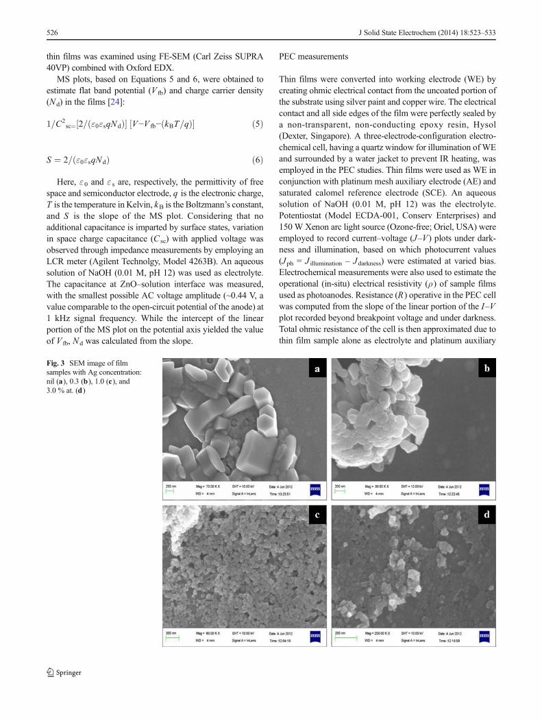
the border of ionic and covalent compounds [16]. In a fewearlier studies, the simultaneous growth of zinc blend ZnO hasbeen reported [32]. However, we found no evidence to thisregard. Average crystallite size (p ) in samples ranged from 22to 47 nm (Table 2). Its variation with increase in Ag concen-tration still followed an irregular pattern. XRD data werefurther utilized to evaluate dislocation density (δ ) and
microstrain (ε ) in the films (Table 2). Ag incorporation in-creased δ and ε in the films at low concentrations of Ag, butthe values decreased at higher concentrations. It is also evidentthat, barring few exceptions, the samples with greater δ and εexhibited retarded crystallite growth [33]. The irregular pat-tern of variation in crystallite size, dislocation density, andmicrostrain suggests some obscure electrochemical kinetic
400 500 600 700 8000
1
420 440 460 480
0.3
0.6
0.9
1.2
1.5
A
Abs
orba
nce
(a.u
.)
Wavelength (nm.)
abcdefg
2.4 2.7 3.0
0
2
4
2.8 2.9 3.0
0.0
0.5
1.0
1.5
2.0
2.5
3.0
B
(h
)2 /(eV2 )
m-2)
Energy (h )/eV
abcdefg
μν
ν
α
Fig. 6 a Absorbance vs.wavelength. b (αhν)2 vs. hυplots: samples with Agconcentration: nil (a), 0.1 (b), 0.3(c), 0.5 (d), 1.0 (e), 3.0 (f),5.0 % at. (g)
J Solid State Electrochem (2014) 18:523–533 529
parameters dominantly regulating the film growth process byelectrodeposition. Further work is needed on it.
Surface characteristics
AFM images (Fig. 2) and scanning electron micrographs(Fig. 3) of samples indicate a homogeneous and porous micro-structure with hexagonal nanocrystallites. The porous micro-structure seen on the surface is probably formed by the coa-lescing of microvoids and may be attributed to the kinetics ofmaterial flow at the electrode surface during crystallization.SEM image data were utilized to derive the tentative distribu-tion of particle size in samples (Fig. 4). The preferred c-axis-oriented vertical growth of nanocrystallites can be seen in AFMimages in conformity to earlier reports on doped/undoped ZnO[18, 34]. The RMS surface roughness of film over a 5×5-μmarea estimated fromAFM data (Table 2) varied irregularly, with1 and 5 % Ag-incorporated films exhibiting lowest roughness.To investigate atomic and compound percentages, i.e., thestoichiometry of prepared samples, 0.1 and 0.5 % at. Ag-
incorporated ZnO films were subjected to EDX measurement.In the observed EDX spectrum (Fig. 5), the peaks associatedwith Zn, O, and Ag atoms are observed. The atomic percentageof Zn and O elements is about Zn/O=1:1.5 (± 4–8 % experi-mental error) (Table 3). The percentage of O being nearly oneand a half times to that of Zn is attributable to the part contri-bution coming from the underlying substrate. EDX recordedatomic percentage of Ag in samples is agreeable to the amountadded during sample synthesis.
Optical characteristics
UV–vis absorption spectra of films (Fig. 6a) indicate anabsorption threshold at around 400 nm, which may be dueto the onset of fundamental absorption corresponding to O/2pZn/4 s charge transfer band, which is widely reported inliterature for ZnO. Significant gain in absorption along withslight shift in absorption threshold to higher wavelengths till1 % Ag incorporation is also evident. In samples with higherconcentrations of Ag, the absorption magnitude decreased.Changes in crystallinity and stoichiometry are seemingly ma-jor factors controlling the absorption by samples in this study[35]. Corresponding to the absorption edge, bandgap (Eg)values were determined by plotting (αhν)2 versus (hν)(Fig. 6b). The values (Table 2) are close to the reported valuefor bulk ZnO. Ag incorporation led to a significant decrease inEg. However, varying the Ag concentration in samples had atrivial effect on Eg. In the present study, XRD and EDXanalysis did not unequivocally rule out the possible existenceof AgxO phases in Ag-incorporated ZnO films, especially athigher concentrations of Ag. A significant reduction in bandgap energy with 0.1 % at. Ag incorporation and subsequentlyinsignificant variation on further increase in Ag concentrationcan be seen as fallout of the cited possibility. It will bepertinent to mention here that AgxO is absorbed in the visibleregion with direct band gap varying over a wide range of 1.2–3.4 eV. Such wide band gap range in AgxO is due to thedifferent stoichiometries, crystalline phases, and propertiesarising from different deposition techniques [36].
-1.0 -0.5 0.0 0.5 1.06
4
2
0
Applied Potential/ (V/SCE)
Cu
rren
t (m
A /c
m2 )
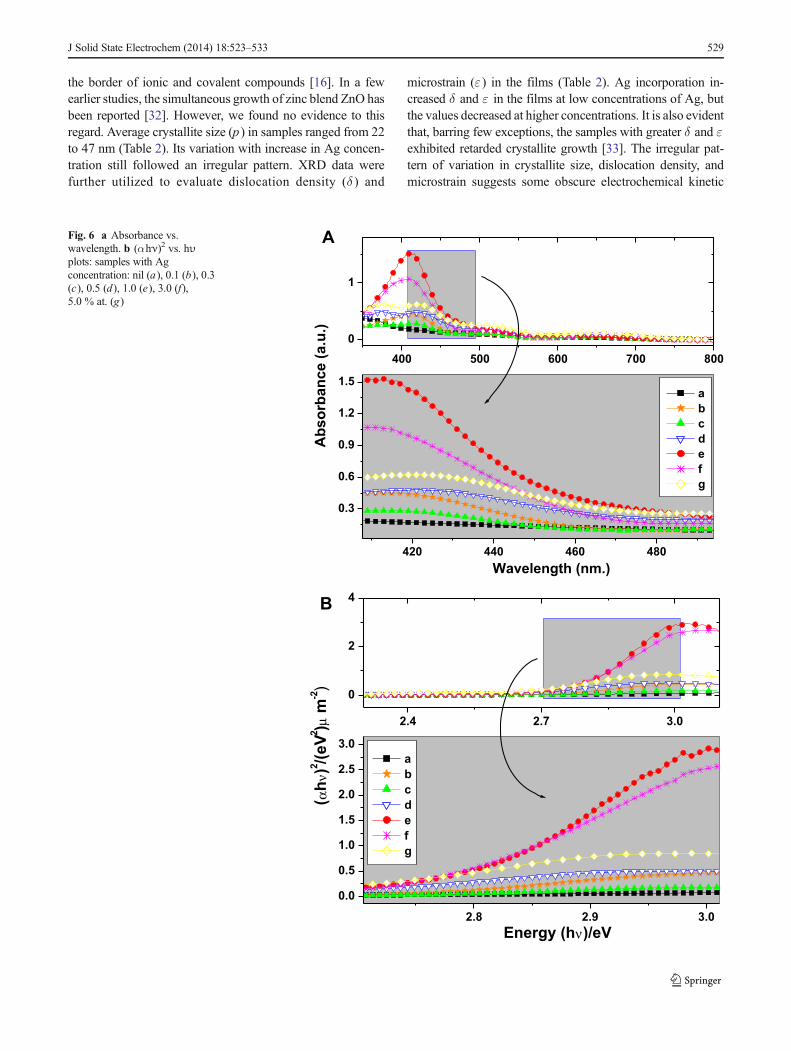
Under Darknessabcdefg
Fig. 7 Variation in current density with applied potential, under darknessand illumination: samples with Ag concentration: nil (a), 0.1 (b), 0.3 (c),0.5 (d), 1.0 (e), 3.0 (f), 5.0 % at. (g)
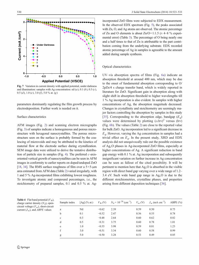
Table 4 Flat band potential (V fb),charge carrier density (Nd), open-circuit voltage (Voc), short-circuitcurrent (Jsc), and ABPE values
Sample index [Ag] (% at.) V fb (V) Nd × 10−20 (cm−3) Voc (V) Jsc (mA cm−2) ABPE (%)
a Nil −0.62 2.39 0.59 0.50 0.75
b 0.1 −0.52 2.47 0.56 0.55 0.78
c 0.3 −0.48 2.64 0.60 0.62 0.82
d 0.5 −0.31 3.75 0.60 0.78 1.01
e 1.0 −0.55 3.98 0.59 0.81 1.23
f 3.0 −0.51 3.34 0.60 0.58 0.99
g 5.0 −0.50 3.28 0.53 0.49 0.85
530 J Solid State Electrochem (2014) 18:523–533
Photoelectrochemical studies
Films were of n-type as indicated from the nature of J–Vcurves (Fig. 7) [37]. The dark current was insignificant untilthe breakpoint, suggesting a well-formed depletion layer,which is a typical characteristic of ZnO. Open-circuit voltage(Voc) under illumination (Table 4) is comparable to the valuesreported earlier [38]. Short-circuit current (J sc) increased onAg incorporation, with the highest gain being of the order of60–65 % with 1 % at. Ag-incorporated films (Table 4).Considerable rise in current under illumination indicatedphotoresponse. Since there is no additional redox couple inthe electrolyte, the gain in current under illumination can beattributed to electrochemical splitting of water, which was alsoindicated by evolution of gases in the form of bubbles on theelectrode surface (at V ≥500 mV vs. SCE).
Films with 1 % at. Ag yielded the highest PEC photocur-rent (Jph) (Fig. 8). The effect may be largely attributed to theexpected increase in photogenerated charge carriers and theirswift separation/migration across the depletion layer and inthe bulk of the semiconductor, facilitated by the efficientabsorption of light and significantly reduced electrical resis-tivity in such samples. Well-aligned band edges with redoxlevels for hydrogen and oxygen evolution are also indicatedfrom significantly high short-circuit currents with this set ofsamples. Variation in Jph and J sc on Ag incorporation follow-ed a similar trend. Results indicate clearly the role of light incurrent generation, with Ag-incorporated samples being betterphotosensitive. Film samples were observed to be electro-chemically stable with no loss of photoactivity even after15–20 repeated runs spread over a period of 1 month. ThePEC photocurrent (Jph) values at 500 mV bias were utilized toevaluate applied bias photon-to-current efficiency ABPE. Thehighest achieved efficiency of 1.23 % (Table 4) was with
1 % at. Ag-incorporated films. Besides efficiency, stabilityof photoelectrodes in PEC cell is also important. In this case,using 3 % at. Ag-doped ZnO thin films, nearly stable photo-currents were recorded up to 3 h of illumination. Observationsmade under chopped illumination also highlight the role oflight in photocurrent generation (Fig. 10).
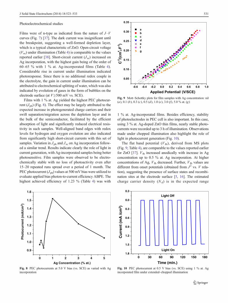
The flat band potential (V fb), derived from MS plots(Fig. 9; Table 4), are comparable to the values reported earlierfor ZnO [37]. V fb increased anodically with increase in Agconcentration up to 0.5 % at. Ag incorporation. At higherconcentrations of Ag, V fb decreased. Further, V fb values aredifferent from onset potentials (obtained from J2 vs. V rela-tion), suggesting the presence of surface states and recombi-nation sites at the electrode surface [5, 16]. The estimatedcharge carrier density (N d) is in the expected range
0 30 60 90 120 150 1801.8
1.5
1.2
0.9
0.6
0.3
0.0
0.3
Cu
rren
t (m
A /c
m2 )
Light On
Light Off
Time (min.)Fig. 10 PEC photocurrent at 0.5 V bias (vs. SCE) using 1 % at. Agincorporated film under extended–chopped illumination
-0.6 -0.4 -0.2 0.0 0.2 0.4 0.6 0.8 1.0
0.05
0.10
0.15
0.20
0.25
0.30
0.35
Applied Potential/ (V/SCE)
C-2/(c
m4
F-2)
abcdefgμ
Fig. 9 Mott–Schottky plots for film samples with Ag concentration: nil(a), 0.1 (b), 0.3 (c), 0.5 (d), 1.0 (e), 3.0 (f), 5.0 % at. (g)
0 1 2 3 4 5
0.9
1.0
1.1
1.2
1.3
1.4
1.5
1.6
Ph
oto
curr
ent
(mA
/cm
2 )
Ag Concentration (% at.)
Fig. 8 PEC photocurrents at 5.0 V bias (vs. SCE) as varied with Agincorporation
J Solid State Electrochem (2014) 18:523–533 531

(Table 4). Illumination led to an increase in Nd by a factor of1.26–1.52, but V fb remained almost unaffected. The observa-tion is in agreement to the previous results [39]. Ag incorpo-ration resulted in increase in Nd, with 1 % Ag-incorporatedsample exhibiting the highest value. Considering the domi-nant existence of Ag in monovalent state, compared to thebivalent state of Zn, two Ag ions substituting Zn ion areexpected to generate one native defect (oxygen vacancy) inthe sample. Hence, a rise in charge carrier density on Agincorporation is understandable. The increase in charge carrierdensity on Ag incorporation is yielding a higher PEC re-sponse, but the increase is not in the same proportion. Thissuggests that for PEC application and photocurrent generation(Fig. 10), besides the concentration of charge carrier, theirmobility is also important. In this study, no attempts weremade to record carrier mobility in the samples, yet it is aknown fact that as the carriers travel through a semiconductor,they encounter various scattering mechanisms that governcarrier mobility in the electronic system. Thus, the higherphotocurrent values recorded with 1 % Ag-incorporated filmsmay be due to obtained synergy in improved optical absorp-tion, increased carrier density, and rise in carrier mobility.Besides the cited effects, the role of incorporated Ag in plas-monic enhanced absorption, surface recombination inhibition,and improved charge transport might also be crucial anddemands further exploration [15]. Carrier mobility still ap-pears to be a critical variant for PEC application.
Conclusions
The present study leads to following conclusions: (1) evolu-tion of nanocrystalline hexagonal wurtzite ZnO structure hasbeen recorded by the preparatory method used; (2) Ag incor-poration caused stoichiometry-dependent significant alter-ations to the microstructural, optical, and semiconductor prop-erties, with repercussions on PEC performance; (3) absorptionspectra and the optical band gap of samples suggest that filmsare efficient UV absorber and moderate to weak absorber ofvisible light. Hence, these can be used for PEC splitting ofwater under UV–visible illumination; (4) Ag incorporation upto 1 % at. Ag caused a significant reduction in density(p ) and electrical resistivity (ρ ), enhanced absorptionalong with marginal red shift to the band gap energy(E g), anodic shift in flat band potential (V fb), and in-creased charge carrier density (N d), enabling 1 % at.Ag-incorporated ZnO films as the most photosensitiveby yielding highest short-circuit current (J sc), photocur-rent density (J ph), and ABPE values; (5) barring fewexceptions, in general, the samples with reduced dislo-cation density (δ ), microstrain (ε ), and surface rough-ness (RMS) generate an increased PEC response.
Acknowledgments Financial assistance from the Department of Atom-ic Energy—Board of Research in Nuclear Sciences, Govt. of India(Project No. 2007/37/44/BRNS/2910) and Department of Science andTechnology, Government of India (Project No. DST/TSG/SH/2011/106)is gratefully acknowledged. The authors are thankful to Dr. Dinesh DevaIIT, Kanpur, India, for SEM and EDX analysis.
References
1. Ohi J (2005) J Mater Res 20:3180–31872. Currao A (2007) Chimia 61:815–8193. Liu X, Wang F, Wang Q (2012) Phys Chem Chem Phys 14:7894–
79114. Kumari S, Tripathi C, Singh AP, Chauhan D, Shrivastav R, Dass S,
Satsangi VR (2006) Curr Sci India 91:1062–10645. Gupta M, Sharma V, Shrivastava J, Solanki A, Singh AP, Satsangi
VR, Dass S, Shrivastav R (2009) Bull Mater Sci 32:23–306. Janotti A, Van de Walle CG (2009) Rep Prog Phys 72:1265017. Mang A, Reimann K, Rubenacke S (1995) Solid State Commun 94:
251–2548. Reynolds DC, Look DC, Jogai B, Litton CW, Cantwell G, Harsch
WC (1999) Phys Rev 60:23409. Meyer BK, Alves H, Hofmann DM, KriegseisW, Forster D, Bertram
F, Christen J, Hoffmann A, Strasburg M, Dworzak M, Haboeck U,Rodina AV (2004) Phys Status Solidi b 241:231–260
10. Bian JC, Li Z, Chen ZD, He HY, Zhang XW, Li X (2011) Appl SurfSci 258:1831–1835
11. Lewandowska A, Kocemba I, Rynkowski J (2008) Polish J EnvironStud 17:433
12. Matsuoka K, Tahara K, Akiyama H, Yamada T (2011) Sunao. JPhotoch Photobio A 221:239–243
13. Arakawa T, Munaoka T, Akiyama T, Yamada S (2009) J Phys ChemC 113:11830–11835
14. Ratyakshi CRP (2009) Asian J Chem 21:11315. Wei Y, Ke L, Kong J, Liu H, Jiao Z, Lu X, Du H, Sun XW (2012)
Nanotechnology 23:23540116. Sharma V, Kumar P, Shrivastava J, Solanki A, Satsangi VR, Dass S,
Shrivastav R (2010) J Mater Sci 46:3792–380117. Sharma V, Kumar P, Shrivastava J, Solanki A, Satsangi VR, Dass S,
Shrivastav R (2011) Int J Hydrogen Energy 36:4280–429018. Sharma V, Kumar P, Singh N, Upadhyay S, Satsangi VR, Dass S,
Shrivastav R (2012) Int J Hydrogen Energy 37:12138–1214919. Shrivastav R, Gupta M, Sharma V, Kumar P, Shrivastava J, Solanki
A, Satsangi VR, Dass S (2011) Int J Nanoparticles 4:248–26720. Scherrer P (1918) Nachr Ges Wiss Gottingn 2:8921. Kathirvel P, Manoharan D, Mohan SM, Kumar S (2009) J
Optoelectron Biomed Mater 1:25–3322. Zhao Y, Zhang J (2008) J Appl Cryst 41:1095–1010823. Ray SC (2001) Sol Energ Mat Sol C 68:307–31224. Singh AP, Kumari S, Shrivastav R, Dass S, Satsangi VR (2009) J
Phys D Appl Phys 42:085303–08530825. Kumari S, Singh AP, Tripathi C, Chauhan D, Dass S, Shrivastav R,
Satsangi VR (2007) Int J Photoenergy 2007:1–626. Chen XB, Jaramillo TF, Deutsch TG, Shwarsctein AK, Forman AJ,
Gaillard A, Garland R, Takanabe K, HeskeC, SunkaraM,McFarlandEW, Domen K, Miller EL, Turner JA, Dinh HN (2010) J Mater Res25:3–16
27. Schoonman J, Krol RV (2011) UPB Sci Bull Series B 73:31–4428. Kutty TRN, Devi GL (1986)Murugaraj.Mat Res Bull 21:1093–110229. Inamdar AI, Mujawar SH, Patil PS (2007) Int J Electrochem Sci 2:
79730. Ba X, Muhler M, Schedel-Niedrig T, Schlogl R (1996) Phys Rev B
54:2249
532 J Solid State Electrochem (2014) 18:523–533

31. Dudeva T, Lima C (2003) J Chinese Chem Soc 50:1093–110232. Kim SK, Jeong SY, Cho CR (2003) Appl Phys Lett 82:56233. Jeyaprakash BG, Kesavan K, Kumar RA, Mohan S, Amalarani A
(2011) Bull Mater Sci 34:60134. Choi SH, Kim JS (2008) Ultramicroscopy 108:128835. Igarashi T, Ihara M, Kusunoki T, Ohno K, Isobe T, Senna M (2000)
Appl Phys Lett 76:1549
36. Hong-Liang F, Xiao-Yong G, Zeng-Yuan Z, Jiao-Min M (2010) JKorean Phys Soc 56:1176–1179
37. Yang X, Wolcott A, Wang G, Sobo A, Fitzmorris RC, Qian F, ZhangJZ, Li Y (2009) Nano Lett 9:2331–2336
38. Singh CB, Singh V, Bhattacharya S, Bhargav PB, Ahmed N (2013)Hindawi Publishing CorporationConference Papers in Energy 2013:1–4
39. Turner JA, Nozik AJ (1982) Appl Phys Lett 41:101–103
J Solid State Electrochem (2014) 18:523–533 533