Embed Size (px)
Citation preview

N
Aa
b
a
ARRA
KCNTS
1
pacactsSssCtpnbIcan
casm
0d
Materials Science and Engineering B 172 (2010) 37–42
Contents lists available at ScienceDirect
Materials Science and Engineering B
journa l homepage: www.e lsev ier .com/ locate /mseb
anocrystalline thin films of CuInS2 grown by spray pyrolysis
shok Kumar Sharmab, Poolla Rajarama,∗
School of Studies in Physics, Jiwaji University, Gwalior 474 011, Madhya Pradesh, IndiaMaharana Pratap College of Technology, Gwalior 474 006, India
r t i c l e i n f o
rticle history:eceived 21 December 2009eceived in revised form 4 April 2010
a b s t r a c t
Nanocrystalline thin films of CuInS2 were grown on glass substrates using the spray pyrolysis technique.An aqueous mixture of solutions of CuCl2, InCl3 and CS(NH2)2 was converted into a fine colloidal solution
ccepted 19 April 2010
eywords:uInS2
anoparticleshin films
by adding acetonitrile, and was then sprayed on to heated glass substrates, to produce the nanocrystallinefilms of CuInS2. The films were characterized using XRD, TEM, electron diffraction, SEM, EDAX, AFM andoptical transmission spectra. AFM and TEM micrographs together with electron diffraction and XRDshow that the films grown in the temperature range 275–325 ◦C are made up of single phase nano-sized(10–25 nm) particles of CuInS2. XRD calculations show that the crystallite size of the films ranges from8 nm to about 15 nm. Optical absorption studies show that the band gap of the sprayed CuInS2 films is in
pray pyrolysis the range 1.48–1.54 eV.
. Introduction
The I–III–IV2 ternary chalcopyrite semiconductors have greatotential for photovoltaic, non-linear, and other optoelectronicpplications [1]. CuInS2 has a theoretically calculated photovoltaiconversion efficiency greater than 26% [2], and along with CuInSe2nd CdTe is among the most important materials for thin film solarells. In the past few years, several researchers have reported onhe synthesis and characterization of polycrystalline CuInS2 usingpray pyrolysis [3–10] as well as various other techniques [11–17].everal reports have appeared on the fabrication of thin film CuInS2olar cells having efficiencies in the 5–11% range [18–22]. Recenttudies have also begun to focus on the synthesis of nanocrystallineuInS2 for solar cell applications. The use of nanostructures in pho-ovoltaics offers the potential for high efficiency by either using newhysical mechanisms or by tailoring material properties. Moreover,anostructures have potentially low fabrication costs, as they cane produced using simple and inexpensive chemical techniques.
t has been reported that dramatic increases in conversion effi-iencies ranging from as much as 60–67% in the ultra-violet rangend as much as 10% in the visible light range occur, when siliconanoparticles are coated on top of silicon solar cells [23].
Nanoparticles of CuInS2 have recently been grown by various
hemical methods. Jiang et al. [24] produced CuInS2 nanorodsnd nanotubes using a solvothermal method. Castro et al. [25]ynthesized colloidal CuInS2 nanocrystals from a single sourceolecular precursor (PPh3)2CuIn(SEt)4. Nairn et al. synthesized∗ Corresponding author. Tel.: +91 7512442785; mobile: +91 9039013886.E-mail address: [email protected] (P. Rajaram).
921-5107/$ – see front matter © 2010 Elsevier B.V. All rights reserved.oi:10.1016/j.mseb.2010.04.012
© 2010 Elsevier B.V. All rights reserved.
CuInS2 nanoparticles by decomposing a molecular precursor usingultra-violet irradiation [26]. Das et al. [27] fabricated nanostruc-tured CuInS2 thin films by an ion layer gas reaction method. Gardneret al. [28] and Peng et al. [29] produced CuInS2 nanocrystals usingmicrowave irradiation. In this paper we present our work on theproperties of nanocrystalline CuInS2 thin films grown by the spraypyrolysis of a colloidal mixture. Colloidal solutions have been usedearlier to synthesize CuInS2 nanoparticles [25,26,28–31], but to thebest of our knowledge, this is the first report on the use of colloidalsolutions to prepare CuInS2 thin films, particularly using the spraymethod.
2. Experimental details
The nanocrystalline CuInS2 films were grown by spraying,through an ultra fine nozzle, a colloidal mixture produced byadding a few drops of acetonitrile to aqueous solutions of CuCl2,InCl3 and CS(NH2)2 and thoroughly stirring the mixture. The col-loidal solution formed is not known but probably could be amixture of complexes like CuCl2(NCCH3)n and InCl3(NCCH3)n [32]along with CS(NH2)2. The films were grown using various sub-strate temperatures ranging from 200 ◦C to 400 ◦C and using aCu/In ratio of unity in the starting solutions. Plane glass slideswere used as the substrates for the thin films. The CuInS2 filmswere characterized by various techniques like X-ray diffraction,SEM (scanning electron microscopy), EDX (energy dispersive anal-
ysis of X-rays), TEM (transmission electron microscopy), AFM(atomic force microscopy) and optical spectra. X-ray diffractionwas performed on a Bruker D8 Advance diffractometer using Cu-K� radiation of wavelength 1.542 Å. SEM and EDX studies werecarried out using a Philips FESEM/EDAX model QUANTA 200 FEG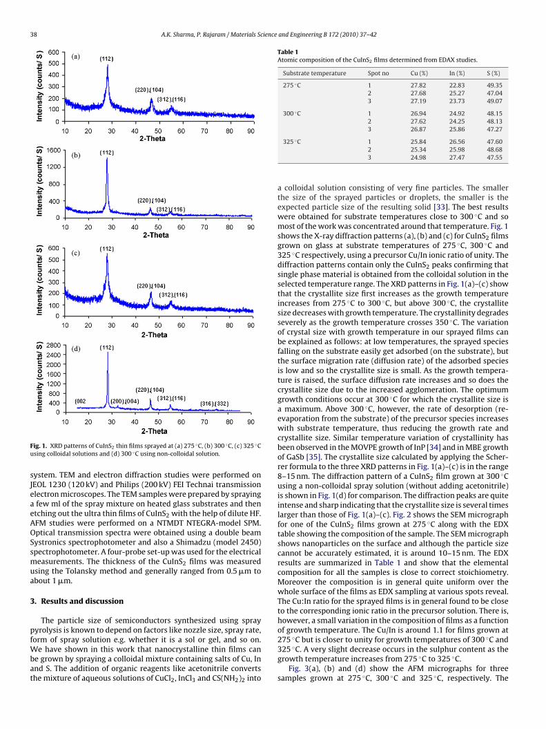
38 A.K. Sharma, P. Rajaram / Materials Science and Engineering B 172 (2010) 37–42
Fu
sJeaeAOSsmua
3
pfWbat
Table 1Atomic composition of the CuInS2 films determined from EDAX studies.
Substrate temperature Spot no Cu (%) In (%) S (%)
275 ◦C 1 27.82 22.83 49.352 27.68 25.27 47.043 27.19 23.73 49.07
300 ◦C 1 26.94 24.92 48.152 27.62 24.25 48.133 26.87 25.86 47.27
ig. 1. XRD patterns of CuInS2 thin films sprayed at (a) 275 ◦C, (b) 300 ◦C, (c) 325 ◦Csing colloidal solutions and (d) 300 ◦C using non-colloidal solution.
ystem. TEM and electron diffraction studies were performed onEOL 1230 (120 kV) and Philips (200 kV) FEI Technai transmissionlectron microscopes. The TEM samples were prepared by sprayingfew ml of the spray mixture on heated glass substrates and thentching out the ultra thin films of CuInS2 with the help of dilute HF.FM studies were performed on a NTMDT NTEGRA-model SPM.ptical transmission spectra were obtained using a double beamystronics spectrophotometer and also a Shimadzu (model 2450)pectrophotometer. A four-probe set-up was used for the electricaleasurements. The thickness of the CuInS2 films was measured
sing the Tolansky method and generally ranged from 0.5 �m tobout 1 �m.
. Results and discussion
The particle size of semiconductors synthesized using sprayyrolysis is known to depend on factors like nozzle size, spray rate,
orm of spray solution e.g. whether it is a sol or gel, and so on.e have shown in this work that nanocrystalline thin films cane grown by spraying a colloidal mixture containing salts of Cu, Innd S. The addition of organic reagents like acetonitrile convertshe mixture of aqueous solutions of CuCl2, InCl3 and CS(NH2)2 into
325 ◦C 1 25.84 26.56 47.602 25.34 25.98 48.683 24.98 27.47 47.55
a colloidal solution consisting of very fine particles. The smallerthe size of the sprayed particles or droplets, the smaller is theexpected particle size of the resulting solid [33]. The best resultswere obtained for substrate temperatures close to 300 ◦C and somost of the work was concentrated around that temperature. Fig. 1shows the X-ray diffraction patterns (a), (b) and (c) for CuInS2 filmsgrown on glass at substrate temperatures of 275 ◦C, 300 ◦C and325 ◦C respectively, using a precursor Cu/In ionic ratio of unity. Thediffraction patterns contain only the CuInS2 peaks confirming thatsingle phase material is obtained from the colloidal solution in theselected temperature range. The XRD patterns in Fig. 1(a)–(c) showthat the crystallite size first increases as the growth temperatureincreases from 275 ◦C to 300 ◦C, but above 300 ◦C, the crystallitesize decreases with growth temperature. The crystallinity degradesseverely as the growth temperature crosses 350 ◦C. The variationof crystal size with growth temperature in our sprayed films canbe explained as follows: at low temperatures, the sprayed speciesfalling on the substrate easily get adsorbed (on the substrate), butthe surface migration rate (diffusion rate) of the adsorbed speciesis low and so the crystallite size is small. As the growth tempera-ture is raised, the surface diffusion rate increases and so does thecrystallite size due to the increased agglomeration. The optimumgrowth conditions occur at 300 ◦C for which the crystallite size isa maximum. Above 300 ◦C, however, the rate of desorption (re-evaporation from the substrate) of the precursor species increaseswith substrate temperature, thus reducing the growth rate andcrystallite size. Similar temperature variation of crystallinity hasbeen observed in the MOVPE growth of InP [34] and in MBE growthof GaSb [35]. The crystallite size calculated by applying the Scher-rer formula to the three XRD patterns in Fig. 1(a)–(c) is in the range8–15 nm. The diffraction pattern of a CuInS2 film grown at 300 ◦Cusing a non-colloidal spray solution (without adding acetonitrile)is shown in Fig. 1(d) for comparison. The diffraction peaks are quiteintense and sharp indicating that the crystallite size is several timeslarger than those of Fig. 1(a)–(c). Fig. 2 shows the SEM micrographfor one of the CuInS2 films grown at 275 ◦C along with the EDXtable showing the composition of the sample. The SEM micrographshows nanoparticles on the surface and although the particle sizecannot be accurately estimated, it is around 10–15 nm. The EDXresults are summarized in Table 1 and show that the elementalcomposition for all the samples is close to correct stoichiometry.Moreover the composition is in general quite uniform over thewhole surface of the films as EDX sampling at various spots reveal.The Cu:In ratio for the sprayed films is in general found to be closeto the corresponding ionic ratio in the precursor solution. There is,however, a small variation in the composition of films as a functionof growth temperature. The Cu/In is around 1.1 for films grown at275 ◦C but is closer to unity for growth temperatures of 300 ◦C and
325 ◦C. A very slight decrease occurs in the sulphur content as thegrowth temperature increases from 275 ◦C to 325 ◦C.Fig. 3(a), (b) and (d) show the AFM micrographs for threesamples grown at 275 ◦C, 300 ◦C and 325 ◦C, respectively. The

A.K. Sharma, P. Rajaram / Materials Science and Engineering B 172 (2010) 37–42 39
s of Cu
mAfsi
Fig. 2. SEM and EDAX image
icrographs clearly show nanoparticles in all the three cases. TheFM images for the sample grown at 300 ◦C are shown at two dif-
erent magnifications in Fig. 3(b) and (c). It can be seen that theurface is uniformly covered with oval shaped particles. The major-ty of the particles have sizes in the range 20–25 nm. A comparison
Fig. 3. AFM micrographs of CuInS2 films sprayed at (a) 275 ◦C, (b
InS2 film sprayed at 275 ◦C.
of the AFM micrographs also shows that the films grown at 300 ◦Chave the best morphology, with the smoothest surface and mostuniform growth. Three dimensional images (not shown here) alsosupport this observation. 3D AFM images also show excess growthin some regions of the surface for the film grown at 275 ◦C. These
) 300 ◦C, (c) 300 ◦C at higher magnification, and (d) 325 ◦C.
40 A.K. Sharma, P. Rajaram / Materials Science and Engineering B 172 (2010) 37–42
F f a Cud
stfigaistwtmfimscsstwf
t2sc
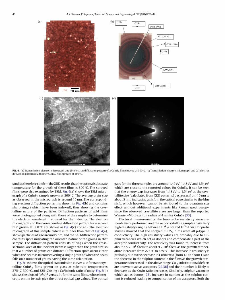
ig. 4. (a) Transmission electron micrograph and (b) electron diffraction pattern oiffraction pattern of a thinner CuInS2 film sprayed at 300 ◦C.
tudies therefore confirm the XRD results that the optimal substrateemperature for the growth of these films is 300 ◦C. The sprayedlms were also examined by TEM. Fig. 4(a) shows the TEM micro-raph of a CuInS2 sample grown at 300 ◦C. The average grain sizes observed in the micrograph is around 15 nm. The correspond-ng electron diffraction pattern is shown in Fig. 4(b) and containsharp rings (which have been indexed), thus showing the crys-alline nature of the particles. Diffraction patterns of gold filmsere photographed along with those of the samples to determine
he electron wavelength required for the indexing. The electronicrograph and the corresponding diffraction pattern for a second
lm grown at 300 ◦C are shown in Fig. 4(c) and (d). The electronicrograph of this sample, which is thinner than that of Fig. 4(a),
hows particles of size around 5 nm, and the SAD diffraction patternontains spots indicating the oriented nature of the grains in thatample. The diffraction pattern consists of rings when the cross-ectional area of the incident beam is larger than the grain size sohat a number of grains can diffract. Diffraction spots occur eitherhen the beam is narrow covering a single grain or when the beam
alls on a number of grains having the same orientation.
Fig. 5(I) shows the optical transmission curves a–c for nanocrys-alline CuInS2 films grown on glass at substrate temperatures75 ◦C, 300 ◦C, and 325 ◦C using a Cu/In ionic ratio of unity. Fig. 5(II)hows the plots of (˛h�)2 versus h� for the same films, whose inter-epts on the h� axis give the direct optical gap values. The optical
InS2 film sprayed at 300 ◦C. (c) Transmission electron micrograph and (d) electron
gaps for the three samples are around 1.49 eV, 1.48 eV and 1.54 eV,which are close to the reported values for CuInS2. It can be seenthat the energy gap increases from 1.48 eV to 1.54 eV as the crys-tallite size (calculated from XRD patterns) decreases from 15 nm toabout 8 nm, indicating a shift in the optical edge similar to the blueshift, which however, cannot be attributed to the quantum sizeeffect without additional experiments like Raman spectroscopy,since the observed crystallite sizes are larger than the reportedWannier–Mott exciton radius of 4 nm for CuInS2 [30].
Electrical measurements like four-probe resistivity measure-ments were performed and the nanocrystalline samples have veryhigh resistivity ranging between 104 � cm and 105 � cm. Hot probestudies showed that the sprayed CuInS2 films were all p-type inconductivity. The high resistivity values are probably due to sul-phur vacancies which act as donors and compensate a part of theacceptor conductivity. The resistivity was found to increase fromabout 2.5 × 10⁴ � cm to about 9 × 10⁴ � cm as the growth temper-ature increased from 275 ◦C to 325 ◦C. This increase in resistivity isprobably due to the decrease in Cu/In ratio (from 1.1 to about 1) andthe decrease in the sulphur content in the films as the growth tem-
perature is increased in the above range. CuIn substitutional defectsare known to act as acceptors [22,36] and their number is likely todecrease as the Cu/In ratio decreases. Similarly, sulphur vacancieswhich act as donors [22], increase in number as the sulphur con-tent is reduced leading to compensation of the acceptors. Both the
A.K. Sharma, P. Rajaram / Materials Science and Engineering B 172 (2010) 37–42 41
Fig. 5. (I) Transmission spectra of nanocrystalline CuInS2 films sprayed at (a) 275 ◦C, (b) 300 ◦C and (c) 325 ◦C and (II) (˛h�)2 versus h� plots for the films grown at (a) 275 ◦C:E
asbmgbiefcmocrv
4
wststtsc8ff
A
DfaswRs
[
[
[[[
[[
[[
[
[
[
[[
[
[
[
g = 1.49 eV, (b) 300 ◦C: Eg = 1.48 eV and (c) 325 ◦C: Eg = 1.54 eV.
bove effects give rise to an increase in the resistivity. The crystalliteize can also influence the electrical properties of the films as grainoundary scattering increases with decreasing crystallite size andust be contributing to the observed variation in resistivity with
rowth temperature. Furthermore, secondary phases, not detectedy XRD, may exist in small amounts due to the observed deviations
n stoichiometry, and are also likely to affect the electrical prop-rties of the sprayed films. Finally, as the resistivity was measuredrom the surface by four-point method, the possibility of the surfaceomposition varying with growth conditions and thus affecting theeasured resistivity values cannot be ruled out. Preliminary work
n p–n junctions of nanocrystalline CuInS2 with sprayed CdS indi-ates a strong photovoltaic effect with open circuit voltages in theange 0.5–0.6 V, but with very poor short circuit currents due to theery high series resistance.
. Conclusions
In conclusion, single phase nanocrystalline CuInS2 thin filmsere prepared, in the temperature range 275–325 ◦C, using the
pray pyrolysis technique. The spray solution was a colloidal mix-ure obtained by adding a few drops of acetonitrile to an aqueousolution mixture containing CuCl2, InCl3 and CS(NH2)2. EDX spec-ra show that the CuInS2 films grown have uniform compositionhroughout the area of the films. SEM, TEM and AFM micrographshow that the particle size of the films is around 10–25 nm. XRDalculations show that the crystallite size of the films ranges fromnm to about 15 nm. The optical gap of the CuInS2 films ranges
rom 1.48 eV to 1.54 eV and is within the reported range of valuesor CuInS2.
cknowledgements
We are grateful to Dr. Ramesh Chandra, IIC, IIT Roorkee and theirector IIT R, for providing the XRD, SEM, EDAX, AFM and TEM
acilities. We are also grateful to Mr. S.D. Sharma, Mr. Shiv Kumar,
nd Mr. Birender Dutt for performing the above experiments. TEMtudies were also performed at Jiwaji University, Gwalior for whiche are thankful to our Electron Microscope Facility. We thank Dr.adha Tomar, School of Studies in Chemistry, Jiwaji University, forome of the optical measurements.[[
[[
References
[1] J.L. Shay, J.H. Wernick, Ternary Chalcopyrites Semiconductors: Growth Elec-tronic Properties and Applications, Pergamon Press, New York, 1975.
[2] L.L. Kazmerski, “Solar Materials Sciences”. Introduction to Photovoltaics PhysicsMaterials and Technology, Academic Press Inc, New York, 1980.
[3] Y.D. Tembhurkar, J.P. Hirde, Bull. Mater. Sci. 16 (3) (1993) 177–185.[4] M. Krunks, O. Bijakina, T. Varema, V. Mikli, E. Mellikov, Thin Solid Films 338
(1999) 125–130.[5] M. Krunks, V. Mikli, O. Bijakina, H. Rebane, A. Mere, T. Varema, E. Mellikov, Thin
Solid Films 361–362 (2000) 61–64.[6] M. Krunks, O. Bijakina, V. Mikli, H. Rebane, T. Varema, M. Altosaar, E. Mellikov,
Solar Energy Mater. Solar Cells 69 (2001) 93–98.[7] M. Krunks, O. Kijatkina, H. Rebane, I. Oja, V. Mikli, A. Mere, Thin Solid Films
403–404 (2002) 71–75.[8] I. Oja, M. Nanu, A. Katerski, M. Krunks, A. Mere, J. Raudoja, A. Goossens, Thin
Solid Films 480–481 (2005) 82–86.[9] T. Terasako, Y. Uno, S. Inoue, T. Kariya, S. Shirakata, Phys. Stat. Sol. (C) 3 (8)
(2006) 2588–2591.10] Morales-Acevedo, M. Orrtega-Lopez, 4th International Conference on Electri-
cal and Electronics Engineering (ICEEE-2007), Mexico City, Mexico, September5–7, 2007.
11] P. Guha, D. Das, A.B. Maity, D. Ganguli, S. Chaudhuri, Solar Energy Mater. SolarCells 80 (2003) 115–130.
12] S. Nakamura, S. Ando, J. Phys. Chem. Solids 66 (2005) 1944–1946.13] J. Podder, T. Miyawaki, M. Ichimura, J. Crystal Growth 275 (2005) e937–e942.14] H. Michael, C. Jin, K.K. Banger, J.D. Harris, A.F. Hepp, Mater. Sci. Eng. B 116 (2005)
395–401.15] X. Hou, K.L. Choy, Thin Solid Films 480–481 (2005) 13–18.16] B. Asenjo, A.M. Chaparro, M.T. Gutierrez, J. Herrero, Thin Solid Films 511 (2006)
117–120.17] X. Liu, L. Shao, Surface Coat. Technol. 201 (2007) 5340–5343.18] R. Scheer, T. Walter, H.W. Schock, M.L. Fearheiley, H.J. Lewerenz, Appl. Phys.
Lett. 63 (24) (1993) 3294–3296.19] D. Braunger, D. Hariskos, T. Walter, H.W. Schock, Solar Energy Mater. Solar Cells
40 (2) (1996) 97–102.20] J. Penndorf, M. Winkler, O. Tober, D. Roser, K. Jacobs, Solar Energy Mater. Solar
Cells 53 (1998) 285–298.21] T.T. John, M. Mathew, C.S. Kartha, K.P. Vijayakumar, T. Abe, Y. Kashiwaba, Solar
Energy Mater. Solar Cells 89 (1) (2005) 27–36.22] A. Goossens, J. Hofhuis, Nanotechnology 19 (2008) 424018–424025.23] M. Stupca, M. Alsalhi, T. Al Saud, A. Almuhanna, M.H. Nayfeh, Appl. Phys. Lett.
91 (6) (2007) 063107.24] Y. Jiang, Y. Wu, S. Yuan, B. Xie, S. Zhang, Y. Qian, J. Mater. Res. 16 (2001)
2805–2809.25] S.L. Castro, S.G. Bailey, R.P. Raffaelle, K.K. Banger, A.F. Hepp, J. Phys. Chem. B 108
(33) (2004) 12429–12435.26] J.J. Nairn, P.J. Shapiro, B. Twamley, T. Pounds, R. Von Wandruszka, T.R. Fletcher,
M. Williams, C. Wang, M.G. Norton, Nano Lett. 6 (6) (2006) 1218–1223.
27] K. Das, S.K. Panda, S. Chaudhuri, Appl. Surf. Sci. 253 (2007) 5166–5172.28] J.S. Gardner, E. Shurdha, C. Wang, L.D. Lau, R.G. Rodriguez, J.J. Pak, J. Nanopart.Res. 10 (4) (2008) 633–641.29] S. Peng, J. Liang, L. Zhang, Y. Shi, J. Chen, J. Chem. Phys. 129 (2008) 134709.30] H. Zhong, Y. Zhou, M. Ye, Y. He, J. Ye, C. He, C. Yang, Y. Li, Chem. Mater. 20 (2008)
6434–6443.

4 ience and Engineering B 172 (2010) 37–42
[
[
[
2 A.K. Sharma, P. Rajaram / Materials Sc
31] F.M. Courtel, R.W. Paynter, B. Marsan, M. Morin, Chem. Mater. 21 (2009)3752–3762.
32] H.L. Hwang, C.Y. Sun, C.S. Fang, S.D. Chang, C.H. Cheng, M.H. Yang, H.H. Lin, H.Tuwan-Mu, J. Crystal Growth 55 (1981) I16–124.
33] K. Okuyama, I.W. Lenggoro, Chem. Eng. Sci. 58 (2003) 537–547.
[[
[
34] N.Y. Li, H.K. Dong, W.S. Wong, C.W. Tu, J. Crystal Growth 164 (1996) I12–116.35] K. Akahane, N. Yamamoto, S. Gozu, N. Ohtani, J. Crystal Growth 264 (2004)
21–25.36] S.M. Wasim, Solar Cells 16 (1986) 289–316.