Embed Size (px)
Citation preview
Appl. Phys. Lett. 118, 210501 (2021); https://doi.org/10.1063/5.0054114 118, 210501
© 2021 Author(s).
Myths and truths about optical phase changematerials: A perspectiveCite as: Appl. Phys. Lett. 118, 210501 (2021); https://doi.org/10.1063/5.0054114Submitted: 14 April 2021 . Accepted: 11 May 2021 . Published Online: 26 May 2021
Yifei Zhang, Carlos Ríos, Mikhail Y. Shalaginov, Mo Li, Arka Majumdar, Tian Gu, and Juejun Hu
Myths and truths about optical phase changematerials: A perspective
Cite as: Appl. Phys. Lett. 118, 210501 (2021); doi: 10.1063/5.0054114Submitted: 14 April 2021 . Accepted: 11 May 2021 .Published Online: 26 May 2021
Yifei Zhang,1 Carlos R�ıos,1 Mikhail Y. Shalaginov,1 Mo Li,2,3 Arka Majumdar,2,3 Tian Gu,1,4,a)
and Juejun Hu1,4,a)
AFFILIATIONS1Department of Materials Science and Engineering, Massachusetts Institute of Technology, Cambridge, Massachusetts 02139, USA2Department of Electrical and Computer Engineering, University of Washington, Seattle, Washington 98195, USA3Department of Physics, University of Washington, Seattle, Washington 98195, USA4Materials Research Laboratory, Massachusetts Institute of Technology, Cambridge, Massachusetts 02139, USA
a)Authors to whom correspondence should be addressed: [email protected] and [email protected]
ABSTRACT
Uniquely furnishing giant and nonvolatile modulation of optical properties and chalcogenide phase change materials (PCMs) have emergedas a promising material to transform integrated photonics and free-space optics alike. The surge of interest in these materials warrants a thor-ough understanding of their characteristics specifically in the context of photonic applications. This article seeks to clarify some commonlyheld misconceptions about PCMs and offer a perspective on new research frontiers in the field.
Published under an exclusive license by AIP Publishing. https://doi.org/10.1063/5.0054114
INTRODUCTION
Chalcogenide phase change materials (PCMs) exemplified byGe2Sb2Te5 (GST-225) represent a class of materials whose electronic andoptical characteristics change drastically when undergoing anamorphous-crystalline phase transition. This singular attribute underpinstheir commercial adoption in the nonvolatile electronic data storage, forexample, Intel’s Optane
TM
memories. Inspired by this success, photonicsnaturally represents the next realm where PCMs can make an impact.Indeed, the past few years have witnessed rapid expansion of researchexplorations in PCM-based photonics with diverse applications spanningoptical switching,1–8 photonic memory,9 optical computing,10–14 activemetamaterial/metasurface,15–25 reflective display,26,27 and thermal cam-ouflage.28,29 These optical device implementations, however, presentunique challenges and requirements often distinctively different fromthose accepted for electronic memories. It is therefore instructive to eluci-date some common confusions about these materials with respect tophotonic applications, which constitutes the focus of this perspective. Inthe end, we will also offer our perspective on the key technical challengesthat define the path forward toward making a practical impact with opti-cal PCMs and emulating their success paradigm in the memory domain.
OPTICAL CONSTANTS ARE NOT CONSTANT
Optical constants, aka refractive indices of materials, are essentialinputs for photonic designers and are used to lay out the blueprints of
functional devices. However, there is a twist when it comes to PCMs:their optical constants are not constant but rather critically dependenton processing conditions. This is evidenced by the considerable spreadin literature values of PCM optical constants even for well-studiedcompositions such as GST-22530–35 (Fig. 1).
The discrepancy of amorphous phase properties shown in Fig.1(a) can be attributed to the different preparation methods in additionto stoichiometry fluctuations—a universal trait of amorphous materi-als.36 For instance, it is well established that as-deposited amorphousPCM films and re-amorphized films exhibit different characteristics.37
Minor composition deviations in the films from the bulk target mate-rial may have also contributed to the variation.
The property changes of PCM films upon heat treatment (viafurnace annealing, laser excitation, or electrothermal heating) sensi-tively depend on processing conditions, resulting in much largerspread of the crystalline phase optical constants [Fig. 1(b)]. On onehand, intermediate states comprising mixtures of amorphous andcrystalline phases can be formed by controlling the temperature orduration of the heat treatment. Notably, there are two distinctiveforms of intermediate states. When heating of PCM is non-uniform,for example, in laser switching where absorption is localized in thelossy crystalline regions, a well-defined boundary between the twophases emerges and crystallization proceeds in the form of phaseboundary movement.38 Spatially segregated two phase regions can
Appl. Phys. Lett. 118, 210501 (2021); doi: 10.1063/5.0054114 118, 210501-1
Published under an exclusive license by AIP Publishing
Applied Physics Letters PERSPECTIVE scitation.org/journal/apl
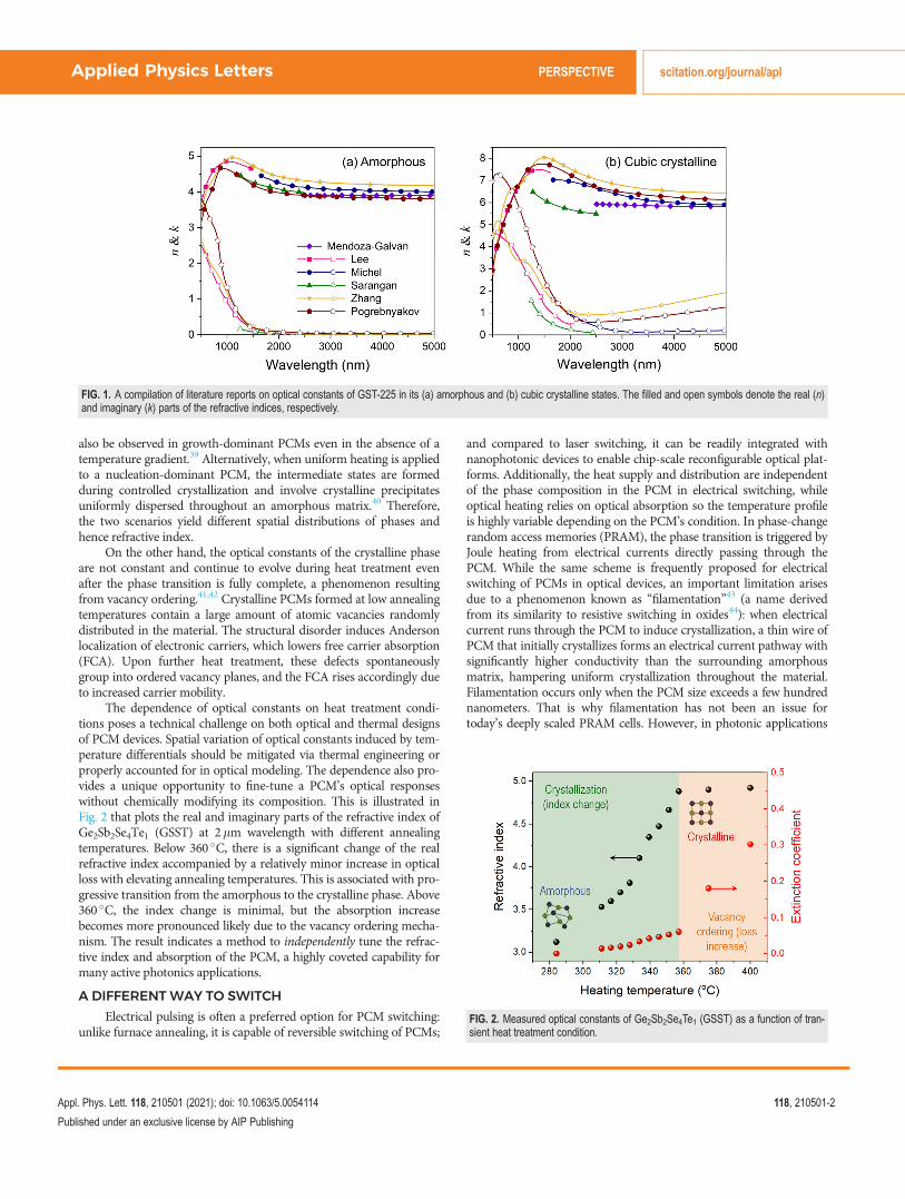
also be observed in growth-dominant PCMs even in the absence of atemperature gradient.39 Alternatively, when uniform heating is appliedto a nucleation-dominant PCM, the intermediate states are formedduring controlled crystallization and involve crystalline precipitatesuniformly dispersed throughout an amorphous matrix.40 Therefore,the two scenarios yield different spatial distributions of phases andhence refractive index.
On the other hand, the optical constants of the crystalline phaseare not constant and continue to evolve during heat treatment evenafter the phase transition is fully complete, a phenomenon resultingfrom vacancy ordering.41,42 Crystalline PCMs formed at low annealingtemperatures contain a large amount of atomic vacancies randomlydistributed in the material. The structural disorder induces Andersonlocalization of electronic carriers, which lowers free carrier absorption(FCA). Upon further heat treatment, these defects spontaneouslygroup into ordered vacancy planes, and the FCA rises accordingly dueto increased carrier mobility.
The dependence of optical constants on heat treatment condi-tions poses a technical challenge on both optical and thermal designsof PCM devices. Spatial variation of optical constants induced by tem-perature differentials should be mitigated via thermal engineering orproperly accounted for in optical modeling. The dependence also pro-vides a unique opportunity to fine-tune a PCM’s optical responseswithout chemically modifying its composition. This is illustrated inFig. 2 that plots the real and imaginary parts of the refractive index ofGe2Sb2Se4Te1 (GSST) at 2lm wavelength with different annealingtemperatures. Below 360 �C, there is a significant change of the realrefractive index accompanied by a relatively minor increase in opticalloss with elevating annealing temperatures. This is associated with pro-gressive transition from the amorphous to the crystalline phase. Above360 �C, the index change is minimal, but the absorption increasebecomes more pronounced likely due to the vacancy ordering mecha-nism. The result indicates a method to independently tune the refrac-tive index and absorption of the PCM, a highly coveted capability formany active photonics applications.
A DIFFERENT WAY TO SWITCH
Electrical pulsing is often a preferred option for PCM switching:unlike furnace annealing, it is capable of reversible switching of PCMs;
and compared to laser switching, it can be readily integrated withnanophotonic devices to enable chip-scale reconfigurable optical plat-forms. Additionally, the heat supply and distribution are independentof the phase composition in the PCM in electrical switching, whileoptical heating relies on optical absorption so the temperature profileis highly variable depending on the PCM’s condition. In phase-changerandom access memories (PRAM), the phase transition is triggered byJoule heating from electrical currents directly passing through thePCM. While the same scheme is frequently proposed for electricalswitching of PCMs in optical devices, an important limitation arisesdue to a phenomenon known as “filamentation”43 (a name derivedfrom its similarity to resistive switching in oxides44): when electricalcurrent runs through the PCM to induce crystallization, a thin wire ofPCM that initially crystallizes forms an electrical current pathway withsignificantly higher conductivity than the surrounding amorphousmatrix, hampering uniform crystallization throughout the material.Filamentation occurs only when the PCM size exceeds a few hundrednanometers. That is why filamentation has not been an issue fortoday’s deeply scaled PRAM cells. However, in photonic applications
FIG. 1. A compilation of literature reports on optical constants of GST-225 in its (a) amorphous and (b) cubic crystalline states. The filled and open symbols denote the real (n)and imaginary (k) parts of the refractive indices, respectively.
FIG. 2. Measured optical constants of Ge2Sb2Se4Te1 (GSST) as a function of tran-sient heat treatment condition.
Applied Physics Letters PERSPECTIVE scitation.org/journal/apl
Appl. Phys. Lett. 118, 210501 (2021); doi: 10.1063/5.0054114 118, 210501-2
Published under an exclusive license by AIP Publishing
where the PCM size is of wavelength scale, Joule heating must rely onan external resistive heater rather than the PCM itself to circumventfilamentation. Reversible electrical switching of PCMs in photonicdevices has been accomplished with micro-heaters made of met-als,23,30,40 doped silicon,45–47 transparent conducting oxides,3 and gra-phene.48 The only exception to the rule is a plasmonic nanogap device,where the PCM volume is minimized via sub-diffraction-limited plas-monic light confinement.49 The PCM can also be reduced tosubwavelength-scale structures as the optical mode is only sensitive totheir collective optical properties.5,14 In this way, each PCM element ina subwavelength-scale structure is independently switched by electro-thermal heating with a much smaller volume, and thus the switchingperformance in terms of speed and repeatability is enhanced whileeffectively suppressing filamentation.
We also note that the statistical nature of nucleation and filamen-tation processes in nucleation-dominant PCMs may be turned into afeature in a different context, e.g., for generating physical unclonablefunctions.50
THE THICKNESS BARRIER OF SPEED
Reversible switching of PCMs also imposes a limit on the size ofPCM elements—a constraint often unknowingly neglected in thedevice design, particularly in active metasurfaces based on PCMs.
To amorphize the PCM, the material is heated to above itsliquidus temperature and rapidly quenched to “freeze” the liquid-likeamorphous state. In order to ensure that crystallization is kineticallysuppressed, the cooling rate must exceed a threshold value known asthe critical cooling rate.36 The attainable cooling rate in a thick mate-rial becomes limited by thermal conduction since it takes time for heatto escape from its interior to the surface. As a result, for each PCM,there exists a maximum thickness beyond which complete reversibleswitching proves difficult. For GST-225, its fast crystallization kineticsimplies a critical cooling rate of the order of 109 �C/s,51 correspondingto a maximum reversible switching thickness of approximately150nm. Uncoincidentally, reversible switching of GST-225 in pho-tonic devices has only been realized in thin films with sub-100-nmthickness. This thickness limit is generally not a concern for integratedphotonic devices, where the light-PCM interaction can be boostedsimply by increasing path length along a waveguide. In free-space opti-cal devices exemplified by optical metasurfaces, thin film filters and
diffractive optical elements, however, the small thickness bounds thetuning range of optical phase delay, thereby severely compromisingthe device performance. The thickness limit can be relieved by explor-ing PCMs with slower crystallization kinetics or equivalently improvedamorphous phase stability, which however introduces tradeoffs inspeed and energy consumption.
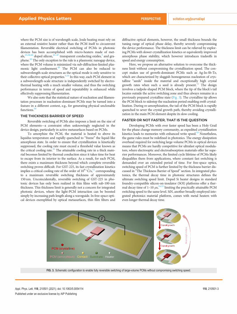
Here, we propose an alternative solution to overcome the thick-ness limit without compromising the crystallization speed. The con-cept makes use of growth-dominant PCMs such as Ag-In-Sb-Te,which are characterized by sluggish homogeneous nucleation of crys-talline “seeds” inside the material and exceptionally high crystalgrowth rates when such a seed is already present.52 The designinvolves a tadpole-shaped PCM block, where the tip of the block’s taillocates outside the active switching zone and thus always remains in apreviously prepared crystalline state (Fig. 3). The crystalline tip allowsthe PCM block to sidestep the nucleation period enabling swift crystal-lization. During re-amorphization, the tail of the PCM block is rapidlyquenched to sever the crystal growth path, thereby avoiding crystalli-zation in the main PCM element despite its slow cooling.
FASTER OR NOT FASTER, THAT IS THE QUESTION
Developing PCMs with ever faster speed has been a Holy Grailfor the phase change memory community, as expedited crystallizationkinetics leads to memories with enhanced write speed.53 Nonetheless,the game rules must be redefined in photonics. The energy dissipationoverhead required for switching large-volume PCMs in optical devicesmeans that PCMs are hardly competitive for ultrafast optical modula-tors, where electrooptic and electroabsorption materials offer far supe-rior performances. Moreover, the limited cycle lifetime of PCMs likelydisqualifies them from applications, where constant fast switching isdemanded over an extended period of time. For free-space optics,switching speed of PCM is further limited by the thickness barrier dis-cussed in “The Thickness Barrier of Speed” section. In integrated pho-tonics, the thermal decay time in photonic structures defines theultimate switching speed limit. Doped Si heater designs in standardfoundry-compatible silicon-on-insulator (SOI) platforms offer a ther-mal decay time of 1–10 ls,54,55 limiting the practically attainable PCMswitching speed to the same level. SiN, another broadly employed inte-grated photonics material platform, comes with metal heaters witheven longer thermal decay time.
FIG. 3. Schematic configuration to enable fully reversible switching of large-volume PCMs without compromising switching speed.
Applied Physics Letters PERSPECTIVE scitation.org/journal/apl
Appl. Phys. Lett. 118, 210501 (2021); doi: 10.1063/5.0054114 118, 210501-3
Published under an exclusive license by AIP Publishing
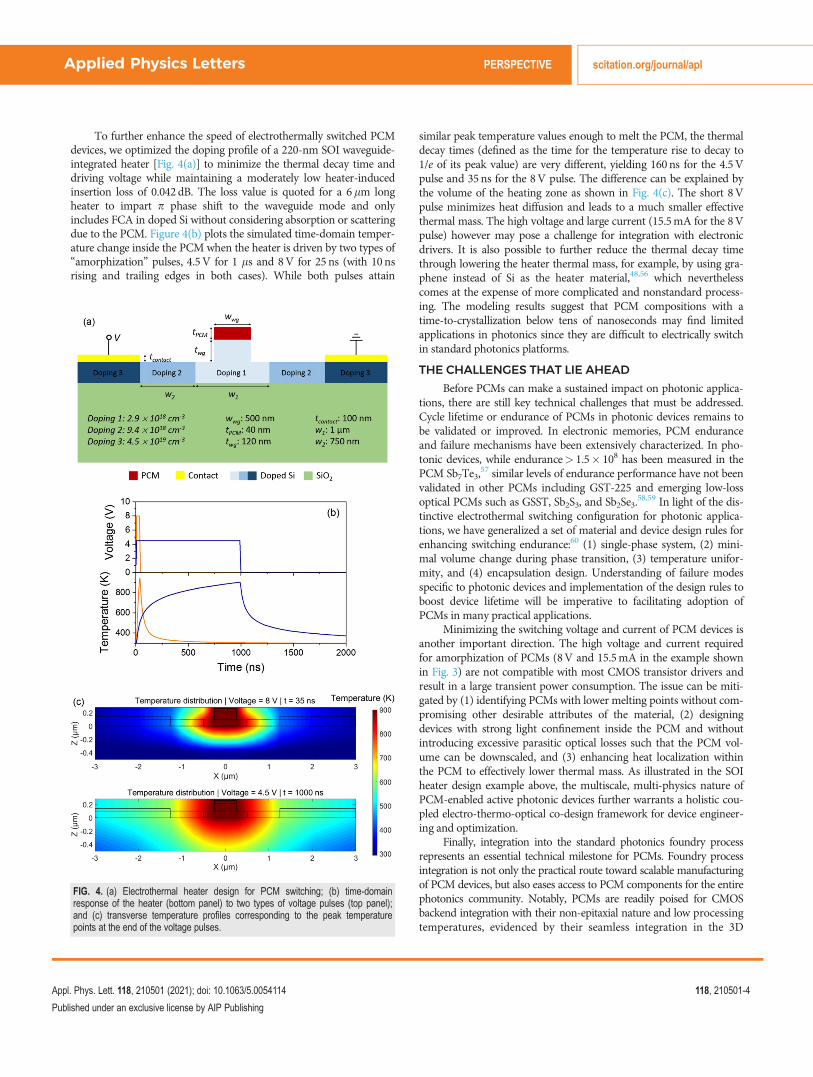
To further enhance the speed of electrothermally switched PCMdevices, we optimized the doping profile of a 220-nm SOI waveguide-integrated heater [Fig. 4(a)] to minimize the thermal decay time anddriving voltage while maintaining a moderately low heater-inducedinsertion loss of 0.042 dB. The loss value is quoted for a 6lm longheater to impart p phase shift to the waveguide mode and onlyincludes FCA in doped Si without considering absorption or scatteringdue to the PCM. Figure 4(b) plots the simulated time-domain temper-ature change inside the PCM when the heater is driven by two types of“amorphization” pulses, 4.5V for 1 ls and 8V for 25 ns (with 10nsrising and trailing edges in both cases). While both pulses attain
similar peak temperature values enough to melt the PCM, the thermaldecay times (defined as the time for the temperature rise to decay to1/e of its peak value) are very different, yielding 160ns for the 4.5Vpulse and 35ns for the 8V pulse. The difference can be explained bythe volume of the heating zone as shown in Fig. 4(c). The short 8Vpulse minimizes heat diffusion and leads to a much smaller effectivethermal mass. The high voltage and large current (15.5mA for the 8Vpulse) however may pose a challenge for integration with electronicdrivers. It is also possible to further reduce the thermal decay timethrough lowering the heater thermal mass, for example, by using gra-phene instead of Si as the heater material,48,56 which neverthelesscomes at the expense of more complicated and nonstandard process-ing. The modeling results suggest that PCM compositions with atime-to-crystallization below tens of nanoseconds may find limitedapplications in photonics since they are difficult to electrically switchin standard photonics platforms.
THE CHALLENGES THAT LIE AHEAD
Before PCMs can make a sustained impact on photonic applica-tions, there are still key technical challenges that must be addressed.Cycle lifetime or endurance of PCMs in photonic devices remains tobe validated or improved. In electronic memories, PCM enduranceand failure mechanisms have been extensively characterized. In pho-tonic devices, while endurance> 1.5� 108 has been measured in thePCM Sb7Te3,
57 similar levels of endurance performance have not beenvalidated in other PCMs including GST-225 and emerging low-lossoptical PCMs such as GSST, Sb2S3, and Sb2Se3.
58,59 In light of the dis-tinctive electrothermal switching configuration for photonic applica-tions, we have generalized a set of material and device design rules forenhancing switching endurance:60 (1) single-phase system, (2) mini-mal volume change during phase transition, (3) temperature unifor-mity, and (4) encapsulation design. Understanding of failure modesspecific to photonic devices and implementation of the design rules toboost device lifetime will be imperative to facilitating adoption ofPCMs in many practical applications.
Minimizing the switching voltage and current of PCM devices isanother important direction. The high voltage and current requiredfor amorphization of PCMs (8V and 15.5mA in the example shownin Fig. 3) are not compatible with most CMOS transistor drivers andresult in a large transient power consumption. The issue can be miti-gated by (1) identifying PCMs with lower melting points without com-promising other desirable attributes of the material, (2) designingdevices with strong light confinement inside the PCM and withoutintroducing excessive parasitic optical losses such that the PCM vol-ume can be downscaled, and (3) enhancing heat localization withinthe PCM to effectively lower thermal mass. As illustrated in the SOIheater design example above, the multiscale, multi-physics nature ofPCM-enabled active photonic devices further warrants a holistic cou-pled electro-thermo-optical co-design framework for device engineer-ing and optimization.
Finally, integration into the standard photonics foundry processrepresents an essential technical milestone for PCMs. Foundry processintegration is not only the practical route toward scalable manufacturingof PCM devices, but also eases access to PCM components for the entirephotonics community. Notably, PCMs are readily poised for CMOSbackend integration with their non-epitaxial nature and low processingtemperatures, evidenced by their seamless integration in the 3D
FIG. 4. (a) Electrothermal heater design for PCM switching; (b) time-domainresponse of the heater (bottom panel) to two types of voltage pulses (top panel);and (c) transverse temperature profiles corresponding to the peak temperaturepoints at the end of the voltage pulses.
Applied Physics Letters PERSPECTIVE scitation.org/journal/apl
Appl. Phys. Lett. 118, 210501 (2021); doi: 10.1063/5.0054114 118, 210501-4
Published under an exclusive license by AIP Publishing
XPoint memory architecture. We foresee that achieving this mile-stone will significantly expedite PCMs’ integration into large switch-ing matrices and open up emerging applications such as arbitrarywavefront synthesis, energy-efficient optical switching and routing,and quantum optical networks as well as scalable neuromorphiccomputing.
ACKNOWLEDGMENTS
This material is based upon the work supported by theDefense Advanced Research Projects Agency through the DefenseSciences Office Program: EXTREME Optics and Imaging(EXTREME) under Agreement No. HR00111720029 and throughthe Young Faculty Award Program under Grant No. D18AP00070.
DATA AVAILABILITY
The data that support the findings of this study are availablefrom the corresponding author upon reasonable request.
REFERENCES1M. Stegmaier, C. R�ıos, H. Bhaskaran, C. D. Wright, and W. H. P. Pernice, Adv.Opt. Mater. 5, 2 (2017).
2M. Rud�e, J. Pello, R. E. Simpson, J. Osmond, G. Roelkens, J. J. G. M. Van DerTol, and V. Pruneri, Appl. Phys. Lett. 103, 141119 (2013).
3K. Kato, M. Kuwahara, H. Kawashima, T. Tsuruoka, and H. Tsuda, Appl.Phys. Express 10, 072201 (2017).
4P. Xu, J. Zheng, J. K. Doylend, and A. Majumdar, ACS Photonics 6, 553 (2019).5C. Wu, H. Yu, H. Li, X. Zhang, I. Takeuchi, and M. Li, ACS Photonics 6, 87(2019).
6Q. Zhang, Y. Zhang, J. Li, R. Soref, T. Gu, and J. Hu, Opt. Lett. 43, 94 (2018).7F. De Leonardis, R. Soref, V. M. N. Passaro, Y. Zhang, and J. Hu, J. Light.Technol. 37, 3183 (2019).
8Y. Zhang and J. Hu, Am. Ceram. Soc. Bull. 99, 36 (2020), see http://web.mit.edu/people/hujuejun/My%20Papers/Journal%20Papers/Reconfigurable%20optics-a%20phase%20change%20for%20the%20better.pdf.
9C. Rios, M. Stegmaier, P. Hosseini, D. Wang, T. Scherer, C. D. Wright, H.Bhaskaran, and W. H. P. Pernice, Nat. Photonics 9, 725 (2015).
10S. Abdollahramezani, O. Hemmatyar, H. Taghinejad, A. Krasnok, Y.Kiarashinejad, M. Zandehshahvar, A. Alu, and A. Adibi, Nanophotonics 9,1189 (2020).
11J. Feldmann, N. Youngblood, M. Karpov, H. Gehring, X. Li, M. L. Gallo, X. Fu,A. Lukashchuk, A. S. Raja, J. Liu, C. D. Wright, A. Sebastian, T. J. Kippenberg,W. H. P. Pernice, and H. Bhaskaran, Nature 589, 52 (2021).
12J. Feldmann, M. Stegmaier, N. Gruhler, C. Ri�os, H. Bhaskaran, C. D. Wright,and W. H. P. Pernice, Nat. Commun. 8, 1256 (2017).
13J. Feldmann, N. Youngblood, C. D. Wright, H. Bhaskaran, and W. H. P.Pernice, Nature 569, 208 (2019).
14C. Wu, H. Yu, S. Lee, R. Peng, I. Takeuchi, and M. Li, Nat. Commun. 12, 96(2021).
15Q. Wang, E. T. F. Rogers, B. Gholipour, C.-M. Wang, G. Yuan, J. Teng, and N.I. Zheludev, Nat. Photonics 10, 60 (2016).
16B. Gholipour, J. Zhang, K. F. MacDonald, D. W. Hewak, and N. I. Zheludev,Adv. Mater. 25, 3050 (2013).
17M. Y. Shalaginov, S. D. Campbell, S. An, Y. Zhang, C. R�ıos, E. B. Whiting, Y.Wu, L. Kang, B. Zheng, C. Fowler, H. Zhang, D. H. Werner, J. Hu, and T. Gu,Nanophotonics 9, 3505 (2020).
18M. Y. Shalaginov, S. An, Y. Zhang, F. Yang, P. Su, V. Liberman, J. B. Chou, C.M. Roberts, M. Kang, C. Rios, Q. Du, C. Fowler, A. Agarwal, K. A. Richardson,C. Rivero-Baleine, H. Zhang, J. Hu, and T. Gu, Nat. Commun. 12, 1225 (2021).
19M. N. Julian, C. Williams, S. Borg, S. Bartram, and H. J. Kim, Optica 7, 746 (2020).20X. Yin, T. Steinle, L. Huang, T. Taubner, M. Wuttig, T. Zentgraf, and H.Giessen, Light Sci. Appl. 6, e17016 (2017).
21C. Ruiz De Galarreta, I. Sinev, A. Alexeev, P. Trofimov, K. Ladutenko, S.Carrillo, E. Gemo, A. Baldycheva, J. Bertolotti, and D. Wright, Optica 7, 476(2020).
22A. Tittl, A. U. Michel, M. Sch€aferling, X. Yin, B. Gholipour, L. Cui, M. Wuttig,T. Taubner, F. Neubrech, and H. Giessen, Adv. Mater. 27, 4597 (2015).
23Y. Wang, P. Landreman, D. Schoen, K. Okabe, A. Marshall, U. Celano, H. S.Philip Wong, J. Park, and M. L. Brongersma, “Electrical tuning of phase-change antennas and metasurfaces,” Nature Nanotechnol. (published online).
24S. Abdollahramezani, O. Hemmatyar, M. Taghinejad, H. Taghinejad, Y.Kiarashinejad, M. Zandehshahvar, T. Fan, S. Deshmukh, A. A. Eftekhar, W.Cai, E. Pop, M. A. El-Sayed, and A. Adibi, Nano Lett. 21, 1238 (2021).
25J. R. Thompson, J. A. Burrow, P. J. Shah, J. Slagle, E. S. Harper, A. VanRynbach, I. Agha, and M. S. Mills, Opt. Express 28, 24629 (2020).
26P. Hosseini, C. D. Wright, and H. Bhaskaran, Nature 511, 206 (2014).27Z. Ni, S. Mou, T. Zhou, and Z. Cheng, Appl. Opt. 57, 3385 (2018).28T. Cao, X. Zhang, W. Dong, L. Lu, X. Zhou, X. Zhuang, J. Deng, X. Cheng, G.Li, and R. E. Simpson, Adv. Opt. Mater. 6, 1800169 (2018).
29Y. Qu, Q. Li, L. Cai, and M. Qiu, Opt. Mater. Express 8, 2312 (2018).30Y. Zhang, J. B. Chou, J. Li, H. Li, Q. Du, A. Yadav, S. Zhou, M. Y. Shalaginov,Z. Fang, H. Zhong, C. Roberts, P. Robinson, B. Bohlin, C. R�ıos, H. Lin, M.Kang, T. Gu, J. Warner, V. Liberman, K. Richardson, and J. Hu, Nat.Commun. 10, 4279 (2019).
31A. Mendoza-Galv�an and J. Gonz�alez-Hern�andez, J. Appl. Phys. 87, 760 (2000).32B. S. Lee, J. R. Abelson, S. G. Bishop, D. H. Kang, B. K. Cheong, and K. B. Kim,J. Appl. Phys. 97, 093509 (2005).
33A.-K. U. Michel, M. Wuttig, and T. Taubner, Adv. Opt. Mater. 5, 1700261 (2017).34A. Sarangan, J. Duran, V. Vasilyev, N. Limberopoulos, I. Vitebskiy, and I.Anisimov, IEEE Photonics J. 10, 1 (2018).
35A. V. Pogrebnyakov, J. A. Bossard, J. P. Turpin, J. D. Musgraves, H. J. Shin, C.Rivero-Baleine, N. Podraza, K. A. Richardson, D. H. Werner, and T. S. Mayer,Opt. Mater. Express 8, 2264 (2018).
36J. D. Musgraves, J. Hu, and L. Calvez, Springer Handbook of Glass, 1st ed.(Springer International Publishing, 2019).
37P. K. Khulbe, E. M. Wright, and M. Mansuripur, J. Appl. Phys. 88, 3926 (2000).38C. Rios, M. Stegmaier, Z. Cheng, N. Youngblood, C. D. Wright, W. H. P.Pernice, and H. Bhaskaran, Opt. Mater. Express 8, 2455 (2018).
39B. S. Lee, R. M. Shelby, S. Raoux, C. T. Retter, G. W. Burr, S. N. Bogle, K.Darmawikarta, S. G. Bishop, and J. R. Abelson, J. Appl. Phys. 115, 063506(2014).
40Y. Zhang, C. Fowler, J. Liang, B. Azhar, M. Y. Shalaginov, S. An, J. B. Chou, C.M. Roberts, V. Liberman, M. Kang, C. R�ı Os, K. A. Richardson, C. Rivero-Baleine, T. Gu, H. Zhang, and J. Hu, “Electrically reconfigurable non-volatilemetasurface using low-loss optical phase-change material,” NatureNanotechnol. (published online).
41W. Zhang, A. Thiess, P. Zalden, R. Zeller, P. H. Dederichs, J. Y. Rat, M. Wuttig,S. Blugel, and R. Mazzarello, Nat. Mater. 11, 952 (2012).
42A. Lotnyk, S. Bern€utz, X. Sun, U. Ross, M. Ehrhardt, and B. Rauschenbach,Acta Mater. 105, 1 (2016).
43M. Wuttig, H. Bhaskaran, and T. Taubner, Nat. Photonics 11, 465 (2017).44Z. Wang, H. Wu, G. W. Burr, C. S. Hwang, K. L. Wang, Q. Xia, and J. J. Yang,Nat. Rev. Mater. 5, 173 (2020).
45H. Zhang, L. Zhou, J. Xu, N. Wang, H. Hu, L. Lu, B. M. A. Rahman, and J.Chen, Sci. Bull. 64, 782 (2019).
46H. Zhang, L. Zhou, L. Lu, J. Xu, N. Wang, H. Hu, B. M. A. Rahman, Z. Zhou,and J. Chen, ACS Photonics 6, 2205 (2019).
47J. Zheng, Z. Fang, C. Wu, S. Zhu, P. Xu, J. K. Doylend, S. Deshmukh, E. Pop, S.Dunham, M. Li, and A. Majumdar, Adv. Mater. 32, 2001218 (2020).
48C. R�ıos, Y. Zhang, M. Y. Shalaginov, S. Deckoff-Jones, H. Wang, S. An, H.Zhang, M. Kang, K. A. Richardson, C. Roberts, J. B. Chou, V. Liberman, S. A.Vitale, J. Kong, T. Gu, and J. Hu, Adv. Photonics Res. 2, 2000034 (2021).
49N. Farmakidis, N. Youngblood, X. Li, J. Tan, J. L. Swett, Z. Cheng, C. D.Wright, W. H. P. Pernice, and H. Bhaskaran, Sci. Adv. 5, eaaw2687 (2019).
50N. Noor and H. Silva, in Springer Series in Advanced Microelectronics (SpringerVerlag, 2020), pp. 59–91.
51H. Y. Cheng, M. Brightsky, S. Raoux, C. F. Chen, P. Y. Du, J. Y. Wu, Y. Y. Lin,T. H. Hsu, Y. Zhu, S. Kim, C. M. Lin, A. Ray, H. L. Lung, and C. Lam, inTechnical Digest - International Electron Devices Meeting (IEDM) (2013).
Applied Physics Letters PERSPECTIVE scitation.org/journal/apl
Appl. Phys. Lett. 118, 210501 (2021); doi: 10.1063/5.0054114 118, 210501-5
Published under an exclusive license by AIP Publishing
52M. Salinga, E. Carria, A. Kaldenbach, M. Bornh€offt, J. Benke, J. Mayer, and M.Wuttig, Nat. Commun. 4, 2371 (2013).
53K. Ding, B. Chen, Y. Chen, J. Wang, X. Shen, and F. Rao, NPG Asia Mater. 12,1 (2020).
54Y. Shen, N. C. Harris, S. Skirlo, M. Prabhu, T. Baehr-Jones, M. Hochberg, X. Sun,S. Zhao, H. Larochelle, D. Englund, and M. Soljacic, Nat. Photonics 11, 441 (2017).
55D. M. Kita, B. Miranda, D. Favela, D. Bono, J. Michon, H. Lin, T. Gu, and J.Hu, Nat. Commun. 9, 1 (2018).
56J. Zheng, S. Zhu, P. Xu, S. Dunham, and A. Majumdar, ACS Appl. Mater.Interfaces 12, 21827 (2020).
57J.-S. Moon, H.-C. Seo, K. K. Son, E. Yalon, K. Lee, E. Flores, G. Candia, and E.Pop, SPIE Proc. 10982, 32 (2019).
58W. Dong, H. Liu, J. K. Behera, L. Lu, R. J. H. Ng, K. V. Sreekanth, X.Zhou, J. K. W. Yang, and R. E. Simpson, Adv. Funct. Mater. 29, 1806181(2019).
59M. Delaney, I. Zeimpekis, D. Lawson, D. W. Hewak, and O. L. Muskens, Adv.Funct. Mater 30, 2002447 (2020).
60C. R�ıos, Y. Zhang, M. Shalaginov, T. Gu, and J. Hu, in Phase Change Materialsin Photonic Computation, edited by H. Bhaskaran and W. Pernice (Elsevier,Amsterdam, Netherlands).
Applied Physics Letters PERSPECTIVE scitation.org/journal/apl
Appl. Phys. Lett. 118, 210501 (2021); doi: 10.1063/5.0054114 118, 210501-6
Published under an exclusive license by AIP Publishing