Embed Size (px)
DESCRIPTION
TDK
Citation preview
73K224BLV.22bis/V.22/V.21/Bell 212A/103
Single-Chip Modem w/ Integrated Hybrid
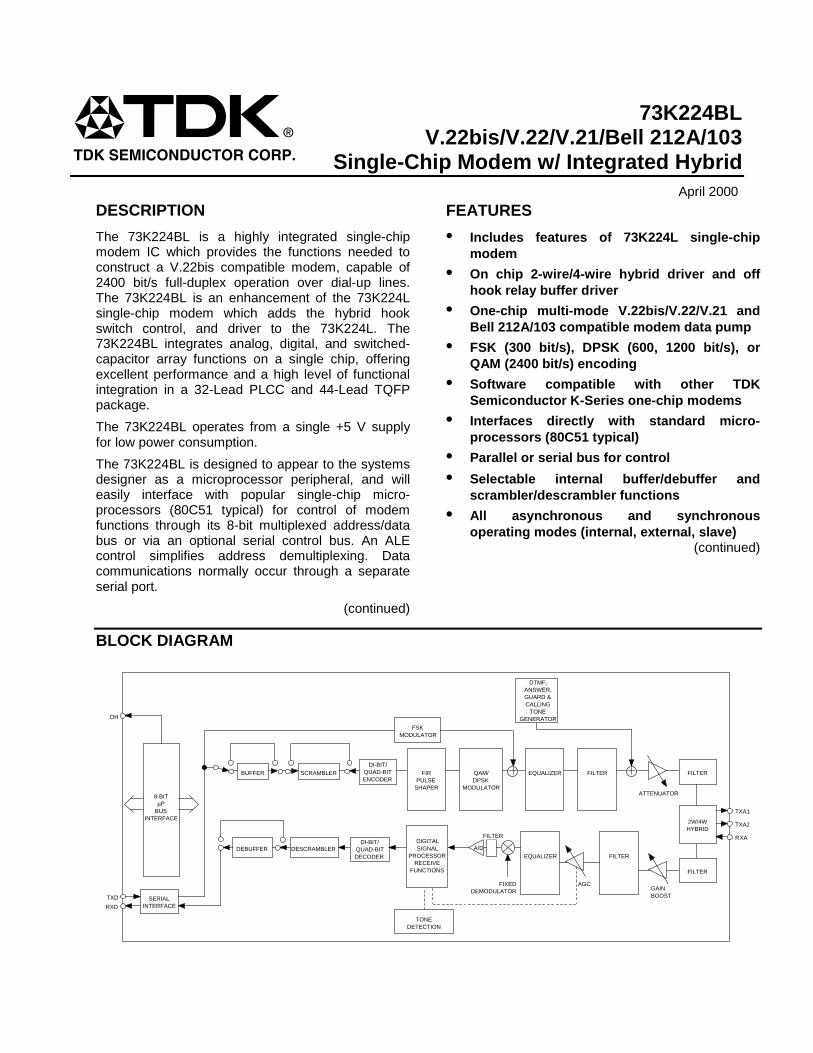
DESCRIPTIONThe 73K224BL is a highly integrated single-chipmodem IC which provides the functions needed toconstruct a V.22bis compatible modem, capable of2400 bit/s full-duplex operation over dial-up lines.The 73K224BL is an enhancement of the 73K224Lsingle-chip modem which adds the hybrid hookswitch control, and driver to the 73K224L. The73K224BL integrates analog, digital, and switched-capacitor array functions on a single chip, offeringexcellent performance and a high level of functionalintegration in a 32-Lead PLCC and 44-Lead TQFPpackage.The 73K224BL operates from a single +5 V supplyfor low power consumption.The 73K224BL is designed to appear to the systemsdesigner as a microprocessor peripheral, and willeasily interface with popular single-chip micro-processors (80C51 typical) for control of modemfunctions through its 8-bit multiplexed address/databus or via an optional serial control bus. An ALEcontrol simplifies address demultiplexing. Datacommunications normally occur through a separateserial port.
(continued)
FEATURES• Includes features of 73K224L single-chip
modem• On chip 2-wire/4-wire hybrid driver and off
hook relay buffer driver• One-chip multi-mode V.22bis/V.22/V.21 and
Bell 212A/103 compatible modem data pump• FSK (300 bit/s), DPSK (600, 1200 bit/s), or
QAM (2400 bit/s) encoding• Software compatible with other TDK
Semiconductor K-Series one-chip modems• Interfaces directly with standard micro-
processors (80C51 typical)• Parallel or serial bus for control• Selectable internal buffer/debuffer and
scrambler/descrambler functions• All asynchronous and synchronous
operating modes (internal, external, slave)(continued)
BLOCK DIAGRAM
April 2000
DI-BIT/QUAD-BITDECODER
TXDRXD
SERIALINTERFACE
BUFFER SCRAMBLERDI-BIT/
QUAD-BITENCODER
FSKMODULATOR
8-BITµP
BUSINTERFACE
DEBUFFER DESCRAMBLER
FIRPULSE
SHAPER
QAM/DPSK
MODULATOR
EQUALIZER FILTER FILTER
FILTER
2W/4WHYBRID
TXA1
TXA2
RXA
FILTEREQUALIZER
DIGITALSIGNAL
PROCESSORRECEIVE
FUNCTIONS
A/D
FILTER
FIXEDDEMODULATOR
AGCGAINBOOST
ATTENUATOR
DTMF,ANSWER,GUARD &CALLING
TONEGENERATOR
TONEDETECTION
OH

73K224BLV.22bis/V.22/V.21/Bell 212A/103Single-Chip Modem w/ Integrated Hybrid
2
DESCRIPTION (continued)
The 73K224BL is pin and software compatible withthe 73K222BL, allowing system upgrades with asingle component change.The 73K224BL is designed to be a completeV.22bis compatible modem on a chip. Thecomplete modem requires only the addition of thephone line interface, a control microprocessor, andRS-232 level converter for a typical system. Manyfunctions were included to simplify implementationof typical modem designs. In addition to the basic2400 bit/s QAM, 600/1200 bit/s DPSK and 300bit/s FSK modulator/demodulator sections, thedevice also includes synch/asynch converters,scrambler/descrambler, call progress tone detect,DTMF tone generator capabilities and handshakepattern detectors. Test features such as analogloop, digital loop, and remote digital loopback aresupported. Internal pattern generators are alsoincluded for self-testing.
FEATURES (continued)• Adaptive equalization for optimum perform-
ance over all lines
• Programmable transmit attenuation (16 dB,1 dB steps), selectable receive boost (+18dB)
• Call progress, carrier, answer tone,unscrambled mark, S1, and signal qualitymonitors
• DTMF, answer and guard tone generators
• Test modes available: ALB, DL, RDL, mark,space, alternating bit, S1 pattern generationand detection
• CMOS technology for low powerconsumption (typically 100 mW @ 5 V) withpower-down mode (15 mW @ 5 V)
• TTL and CMOS compatible inputs andoutputs
FUNCTIONAL DESCRIPTIONHYBRID AND RELAY DRIVERTo make designs more cost effective and spaceefficient, the 73K224BL includes the 2-wire to 4-wire hybrid with sufficient drive to interface directlyto the telecom coupling transformers. In addition,an off hook relay driver with 30mA drive capabilityis also included to allow use of commonlyavailable mechanical telecom relays.
QAM MODULATOR/DEMODULATORThe 73K224BL encodes incoming data into quad-bits represented by 16 possible signal points withspecific phase and amplitude levels. The base-band signal is then filtered to reduce intersymbolinterference on the band limited telephonenetwork. The modulator transmits this encodeddata using either a 1200 Hz (originate mode) or2400 Hz (answer mode) carrier. The demodulator,although more complex, essentially reverses thisprocedure while also recovering the data clockfrom the incoming signal. Adaptive equalizationcorrects for varying line conditions byautomatically changing filter parameters tocompensate for line characteristics.
DPSK MODULATOR/DEMODULATORThe 73K224BL modulates a serial bit stream intodi-bit pairs that are represented by four possiblephase shifts as prescribed by the Bell 212A/V.22standards. The base-band signal is then filtered toreduce intersymbol interference on the bandlimited2-wire PSTN line. Transmission occurs on either a1200 Hz (originate mode) or 2400 Hz carrier(answer mode). Demodulation is the reverse ofthe modulation process, with the incoming analogsignal eventually decoded into di-bits andconverted back to a serial bit stream. Thedemodulator also recovers the clock which wasencoded into the analog signal during modulation.Demodulation occurs using either a 1200 Hzcarrier (answer mode or ALB originate mode) or a2400 Hz carrier (originate mode or ALB answermode). Adaptive equalization is also used inDPSK modes for optimum operation with varyingline conditions.
FSK MODULATOR/DEMODULATORThe FSK modulator produces a frequencymodulated analog output signal using two discretefrequencies to represent the binary data. The Bell103 standard frequencies of 1270 and 1070 Hz

73K224BLV.22bis/V.22/V.21/Bell 212A/103
Single-Chip Modem w/ Integrated Hybrid
3
FUNCTIONAL DESCRIPTION (continued)(originate mark and space) and 2225 and 2025 Hz(answer mark and space) are used when thismode is selected. V.21 mode uses 980 and 1180Hz (originate, mark and space) or 1650 and 1850Hz (answer, mark and space). Demodulationinvolves detecting the received frequencies anddecoding them into the appropriate binary value.The rate converter and scrambler/descrambler areautomatically bypassed in the FSK modes.
PASSBAND FILTERS AND EQUALIZERSHigh and low band filters are included to shape theamplitude and phase response of the transmit andreceive signals and provide compromise delayequalization and rejection of out-of-band signals.Amplitude and phase equalization are necessaryto compensate for distortion of the transmissionline and to reduce intersymbol interference in theband limited receive signal. The transmit signalfiltering corresponds to a 75% square root ofraised Cosine frequency response characteristic.
ASYNCHRONOUS MODEThe asynchronous mode is used for communicationwith asynchronous terminals which maycommunicate at 600,1200, or 2400 bit/s +1%, -2.5% even though the modem’s output is limited tothe nominal bit rate ±.01% in DPSK and QAMmodes. When transmitting in this mode the serialdata on the TXD input is passed through a rateconverter which inserts or deletes stop bits in theserial bit stream in order to output a signal that isthe nominal bit rate ±.01%. This signal is thenrouted to a data scrambler and into the analogmodulator where quad-bit/di-bit encoding results inthe output signal. Both the rate converter andscrambler can be bypassed for handshaking, andsynchronous operation as selected. Received datais processed in a similar fashion except that the rateconverter now acts to reinsert any deleted stop bitsand output data to the terminal at no greater thanthe bit rate plus 1%. An incoming break signal (lowthrough two characters) will be passed throughwithout incorrectly inserting a stop bit.
The synch/asynch converter also has an extendedoverspeed mode which allows selection of an outputoverspeed range of either +1% or +2.3%. In theextended overspeed mode, stop bits are output at 7/8rising edge of TXCLK the normal width.
Both the synch/asynch rate converter and the datadescrambler are automatically bypassed in theFSK modes.
SYNCHRONOUS MODESynchronous operation is possible only in theQAM or DPSK modes. Operation is similar to thatof the asynchronous mode except that data mustbe synchronized to a provided clock and novariation in data transfer rate is allowable. Serialinput data appearing at TXD must be valid on therising edge of TXCLK.TXCLK is an internally derived 1200 or 2400 Hzsignal in internal mode and is connected internallyto the RXCLK pin in slave mode. Receive data atthe RXD pin is clocked out on the falling edge ofRXCLK. The asynch/synch converter is bypassedwhen synchronous mode is selected and data istransmitted at the same rate as it is input.
PARALLEL BUS CONTROL INTERFACE MODEEight 8-bit registers are provided for control, optionselect, and status monitoring. These registers areaddressed with the AD0, AD1, and AD2multiplexed address lines (latched by ALE) andappear to a control microprocessor as sevenconsecutive memory locations. Six controlregisters are read/write memory. The detect andID registers are read only and cannot be modifiedexcept by modem response to monitoredparameters.

73K224BLV.22bis/V.22/V.21/Bell 212A/103Single-Chip Modem w/ Integrated Hybrid
4
SERIAL CONTROL INTERFACE MODEThe serial Command mode allows access to the73K224BL control and status registers via a serialcontrol port. In this mode the AD0, AD1, and AD2lines provide register addresses for data passedthrough the AD7 (DATA) pin under control of theRD and WR lines. A read operation is initiatedwhen the RD line is taken low. The next eightcycles of EXCLK will then transfer out eight bits ofthe selected address location LSB first. A writetakes place by shifting in eight bits of data LSBfirst for eight consecutive cycles of EXCLK. WR isthen pulsed low and data transfer into the selectedregister occurs on the rising edge of WR.
DTMF GENERATORThe DTMF generator controls the sending of thesixteen standard DTMF tone pairs. The tone pairsent is determined by selecting transmit DTMF (bitD4) and the 4 DTMF bits (D0-D3) of the ToneRegister. Transmission of DTMF tones from TXAis gated by the transmit enable bit of CR0 (bit D1)as with all other analog signals.
73K224BLV.22bis/V.22/V.21/Bell 212A/103
Single-Chip Modem w/ Integrated Hybrid
5
PIN DESCRIPTION
POWER
NAME PIN TYPE DESCRIPTIONGND 1 I System groundVDD 16 I Power supply input, 5 V ±10% (73K224BL). Bypass with 0.1
and 22 µF capacitors to GND.VREF 31 O An internally generated reference voltage. Bypass with
0.1 µF capacitor to ground.ISET 28 I Chip current reference. Sets bias current for op-amps. The
chip current is set by connecting this pin to VDD through a2 MΩ resistor. ISET should be bypassed to GND with a0.1 µF capacitor.
PARALLEL MICROPROCESSOR CONTROL INTERFACE MODE
ALE 13 I ADDRESS LATCH ENABLE: The falling edge of ALE latchesthe address on AD0-AD2 and the chip select on CS.
AD0-AD7 5-12 I/O ADDRESS/DATA BUS: These bi-directional tri-statemultiplexed lines carry information to and from the internalregisters.
CS 23 I CHIP SELECT: A low on this pin during the falling edge ofALE allows a read cycle or a write cycle to occur. AD0-AD7will not be driven and no registers will be written if CS(latched) is not active. The state of CS is latched on thefalling edge of ALE.
CLK 2 O OUTPUT CLOCK: This pin is selectable under processorcontrol to be either the crystal frequency (for use as aprocessor clock) or 16 times the data rate for use as a baudrate clock in DPSK modes only. The pin defaults to thecrystal frequency on reset.
INT 20 O INTERRUPT: This open drain output signal is used to informthe processor that a detect flag has occurred. The processormust then read the Detect Register to determine which detecttriggered the interrupt. INT will stay low until the processorreads the detect register or does a full reset.
RD 15 I READ: A low requests a read of the 73K224BL internalregisters. Data can not be output unless both RD and thelatched CS are active or low.
RESET 30 I RESET: An active high signal on this pin will put the chip intoan inactive state. All Control Register bits (CR0, CR1, tone)will be reset. The output of the CLK pin will be set to thecrystal frequency. An internal pull-down resistor permitspower-on-reset using a capacitor to VDD.

73K224BLV.22bis/V.22/V.21/Bell 212A/103Single-Chip Modem w/ Integrated Hybrid
6
PARALLEL MICROPROCESSOR INTERFACE (continued)
NAME PIN TYPE DESCRIPTIONWR 14 I WRITE: A low on this informs the 73K224BL that data is
available on AD0-AD7 for writing into an internal register.Data is latched on the rising edge of WR. No data is writtenunless both WR and the latched CS are low.
SERIAL MICROPROCESSOR CONTROL INTERFACE MODE
NAME PIN TYPE DESCRIPTIONAD0-AD2 5-7 I REGISTER ADDRESS SELECTION: These lines carry
register addresses and should be valid during any read orwrite operation.
DATA (AD7) 12 I/O SERIAL CONTROL DATA: Data for a read/write operation isclocked in or out on the falling edge of the EXCLK pin. Thedirection of data flow is controlled by the RD pin. RD lowoutputs data. RD high inputs data.
RD 15 I READ: A low on this input informs the 73K224BL that data orstatus information is being read by the processor. The fallingedge of the RD signal will initiate a read from the addressedregister. The RD signal must continue for eight falling edgesof EXCLK in order to read all eight bits of the referencedregister. Read data is provided LSB first. Data will not beoutput unless the RD signal is active.
WR 14 I WRITE: A low on this input informs the 73K224BL that dataor status information has been shifted in through the DATApin and is available for writing to an internal register. Thenormal procedure for a write is to shift in data LSB first on theDATA pin for eight consecutive falling edges of EXCLK andthen to pulse WR low. Data is written on the rising edge ofWR.
NOTE: The serial control mode is provided by tying ALE high and CS low. In this configuration AD7 becomesDATA and AD0, AD1 and AD2 become the register address.

73K224BLV.22bis/V.22/V.21/Bell 212A/103
Single-Chip Modem w/ Integrated Hybrid
7
DTE USER
NAME PIN TYPE DESCRIPTIONEXCLK 22 I EXTERNAL CLOCK: This signal is used in synchronous
transmission when the external timing option has beenselected. In the external timing mode the rising edge ofEXCLK is used to strobe synchronous DPSK transmit dataapplied to on the TXD pin. Also used for serial controlinterface.
RXCLK 26 O RECEIVE CLOCK: The falling edge of this clock output iscoincident with the transitions in the serial received dataoutput. The rising edge of RXCLK can be used to latch thevalid output data. RXCLK will be valid as long as a carrier ispresent.
RXD 25 O RECEIVED DATA OUTPUT: Serial receive data is availableon this pin. The data is always valid on the rising edge ofRXCLK when in synchronous mode. RXD will outputconstant marks if no carrier is detected.
TXCLK 21 O TRANSMIT CLOCK: This signal is used in synchronoustransmission to latch serial input data on the TXD pin. Datamust be provided so that valid data is available on the risingedge of the TXCLK. The transmit clock is derived fromdifferent sources depending upon the synchronization modeselection. In internal mode the clock is generated internally.In external mode TXCLK is phase locked to the EXCLK pin.In slave mode TXCLK is phase locked to the RXCLK pin.TXCLK is always active.
TXD 24 I TRANSMIT DATA INPUT: Serial data for transmission isapplied on this pin. In synchronous modes, the data must bevalid on the rising edge of the TXCLK clock. In asynchronousmodes (1200/600 bit/s or 300 baud) no clocking isnecessary. DPSK data must be 1200/600 bit/s +1%, -2.5% or+2.3%, -2.5 % in extended over speed mode.
.

73K224BLV.22bis/V.22/V.21/Bell 212A/103Single-Chip Modem w/ Integrated Hybrid
8
PIN DESCRIPTION (continued)
ANALOG INTERFACE AND OSCILLATOR
NAME PIN TYPE DESCRIPTIONRXA 32 I Received modulated analog signal input from the telephone
line interface.TXA1 / TXA2 18 / 17 O Transmit Analog (differential outputs): These pins provide the
analog output signals to be transmitted to the telephone line.The drivers will differentially drive the impedance of the linetransformer and the line matching resistor. An external hybridcan also be built using TXA1 as a single ended transmitsignal.
XTL1 / XTL2 3 / 4 I These pins are for the internal crystal oscillator requiring a11.0592 MHz parallel mode crystal. Load capacitors shouldbe connected from XTL1 and XTL2 to ground. XTL2 can alsobe driven from an external clock.
OH 27 O OFF-HOOK RELAY DRIVER: This signal is an open drainoutput capable of sinking 30mA and is used for controlling arelay. The output is the complement of the OH register bit inthe ID Register.
.
73K224BLV.22bis/V.22/V.21/Bell 212A/103
Single-Chip Modem w/ Integrated Hybrid
9
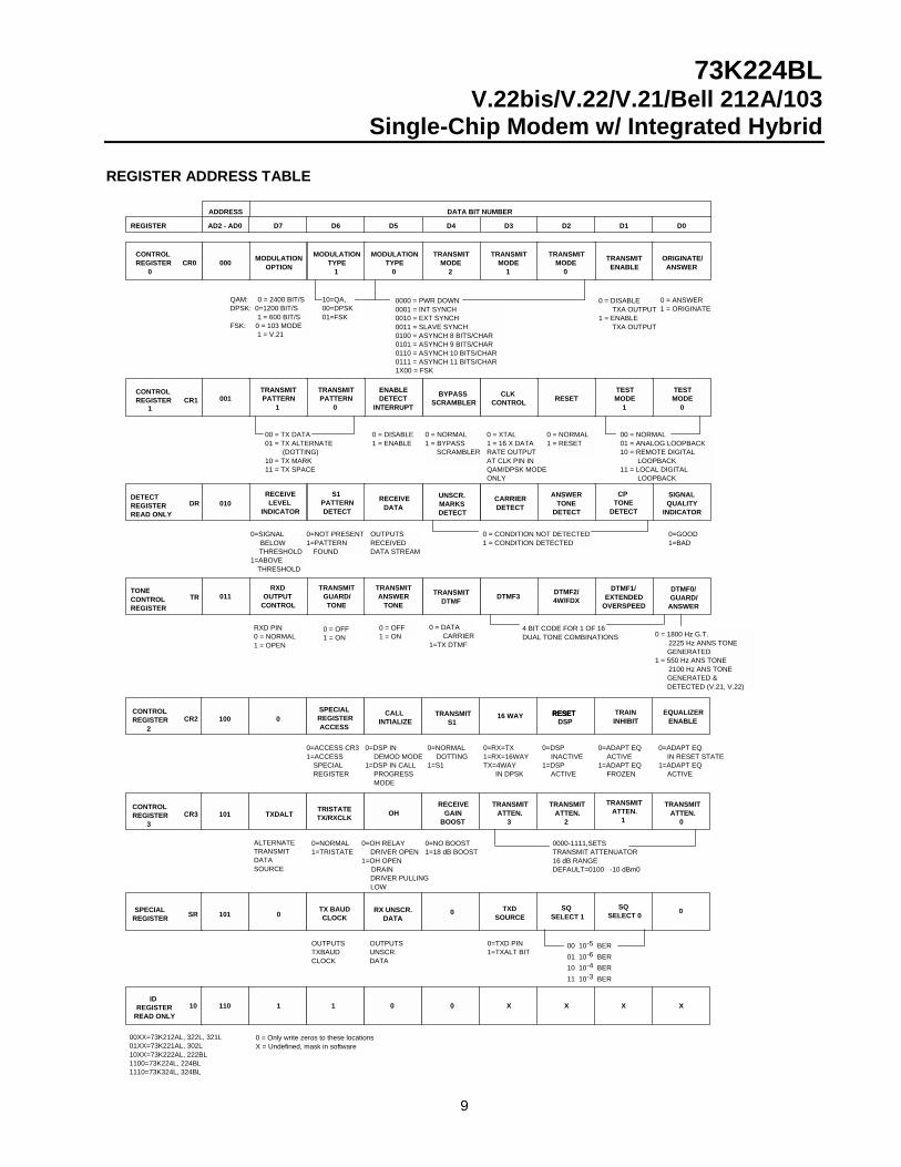
REGISTER ADDRESS TABLE
MODULATION OPTION
00 = NORMAL01 = ANALOG LOOPBACK10 = REMOTE DIGITAL LOOPBACK11 = LOCAL DIGITAL LOOPBACK
CONTROLREGISTER 000
TRANSMITMODE
2
TRANSMITMODE
1
TRANSMITENABLE
ORIGINATE/ANSWER
DATA BIT NUMBER
AD2 - AD0REGISTER
ADDRESS
D7 D6 D5 D4 D3 D2 D1 D0
TESTMODE
0
TESTMODE
1RESETCLK
CONTROLBYPASS
SCRAMBLER
ENABLEDETECT
INTERRUPT
TRANSMITPATTERN
0
TRANSMITPATTERN
1001
CONTROLREGISTER CR1
SIGNALQUALITY
INDICATOR
CPTONE
DETECT
ANSWERTONE
DETECT
CARRIERDETECT
RECEIVEDATA010
DETECTREGISTERREAD ONLY
DR
DTMF0/GUARD/
ANSWER
DTMF1/EXTENDED
OVERSPEED
DTMF2/4W/FDXDTMF3TRANSMIT
DTMF
TRANSMITANSWER
TONE
RXDOUTPUT
CONTROL011
TONECONTROLREGISTER
TR
TRANSMITMODE
0
0000 = PWR DOWN0001 = INT SYNCH0010 = EXT SYNCH0011 = SLAVE SYNCH0100 = ASYNCH 8 BITS/CHAR0101 = ASYNCH 9 BITS/CHAR0110 = ASYNCH 10 BITS/CHAR0111 = ASYNCH 11 BITS/CHAR1X00 = FSK
0 = DISABLE TXA OUTPUT1 = ENABLE TXA OUTPUT
0 = ANSWER1 = ORIGINATE
00 = TX DATA01 = TX ALTERNATE (DOTTING)10 = TX MARK11 = TX SPACE
0 = DISABLE1 = ENABLE
0 = NORMAL1 = BYPASS SCRAMBLER
0 = XTAL1 = 16 X DATARATE OUTPUT AT CLK PIN INQAM/DPSK MODEONLY
0 = NORMAL1 = RESET
OUTPUTSRECEIVEDDATA STREAM
0 = CONDITION NOT DETECTED1 = CONDITION DETECTED
RXD PIN0 = NORMAL1 = OPEN
0 = OFF1 = ON
0 = DATA CARRIER1=TX DTMF
4 BIT CODE FOR 1 OF 16DUAL TONE COMBINATIONS
CR0
QAM: 0 = 2400 BIT/S DPSK: 0=1200 BIT/S 1 = 600 BIT/SFSK: 0 = 103 MODE 1 = V.21
TRANSMITGUARD/TONE
0 = 1800 Hz G.T. 2225 Hz ANNS TONE GENERATED1 = 550 Hz ANS TONE 2100 Hz ANS TONE GENERATED & DETECTED (V.21, V.22)
0 = OFF1 = ON
UNSCR.MARKSDETECT
CONTROLREGISTER
2CR2 100 0
SPECIALREGISTERACCESS
CALLINTIALIZE
TRANSMITS1
S1PATTERNDETECT
RECEIVELEVEL
INDICATOR
16 WAY RESETRESETRESETRESETDSP
TRAININHIBIT
EQUALIZERENABLE
0=ACCESS CR31=ACCESS SPECIAL REGISTER
1
0
MODULATION TYPE
1
MODULATION TYPE
0
10=QA,00=DPSK01=FSK
0=SIGNAL BELOW THRESHOLD1=ABOVE THRESHOLD
0=NOT PRESENT1=PATTERN FOUND
0=GOOD1=BAD
0=DSP IN DEMOD MODE1=DSP IN CALL PROGRESS MODE
0=NORMAL DOTTING1=S1
0=RX=TX1=RX=16WAYTX=4WAY IN DPSK
0=DSP INACTIVE1=DSP ACTIVE
0=ADAPT EQ ACTIVE1=ADAPT EQ FROZEN
0=ADAPT EQ IN RESET STATE1=ADAPT EQ ACTIVE
CONTROLREGISTER
3CR3 101 TXDALT
TRISTATETX/RXCLK OH
RECEIVEGAIN
BOOST
TRANSMITATTEN.
3
TRANSMITATTEN.
2
TRANSMITATTEN.
1
TRANSMITATTEN.
0
ALTERNATETRANSMITDATASOURCE
0=NORMAL1=TRISTATE
0=OH RELAY DRIVER OPEN1=OH OPEN DRAIN DRIVER PULLING LOW
0000-1111,SETSTRANSMIT ATTENUATOR16 dB RANGEDEFAULT=0100 -10 dBm0
0=NO BOOST1=18 dB BOOST
SPECIALREGISTER SR 101 0
TX BAUDCLOCK
RX UNSCR.DATA
0 TXDSOURCE
SQSELECT 1
SQSELECT 0 0
OUTPUTSTXBAUDCLOCK
00 10-5 BER01 10-6 BER10 10-4 BER11 10-3 BER
OUTPUTSUNSCR.DATA
0=TXD PIN1=TXALT BIT
IDREGISTER
READ ONLY10 110 1 1 0 0 X X X X
0 = Only write zeros to these locationsX = Undefined, mask in software
00XX=73K212AL, 322L, 321L01XX=73K221AL, 302L10XX=73K222AL, 222BL1100=73K224L, 224BL1110=73K324L, 324BL

73K224BLV.22bis/V.22/V.21/Bell 212A/103Single-Chip Modem w/ Integrated Hybrid
10
CONTROL REGISTER 0
CR0 D7 D6 D5 D4 D3 D2 D1 D0
ADDR000
MODUL.OPTION
MODUL.TYPE 1
MODUL.TYPE 0
TRANSMITMODE 2
TRANSMITMODE 1
TRANSMITMODE 0
TRANSMITENABLE
ANSWER/ORIGINATE
BIT NAME CONDITION DESCRIPTIOND0 Answer/ 0 Selects answer mode (transmit in high band, receive
Originate in low band).1 Selects originate mode (transmit in low band, receive in
high band).D1 Transmit 0 Disables transmit output at TXA1 & TXA2
Enable 1 Enables transmit output at TXA1 & TXA2Note: Transmit enable must be set to 1 to allowactivation of answer tone or DTMF.
D5,D4 Transmit D5 D4 D3 D2D3,D2 Mode 0 0 0 0 Selects Power down mode. All functions disabled except
digital interface..0 0 0 1 Internal synchronous mode in this mode TXCLK is an
internally derived 600,1200 or 2400 Hz signal. Serialinput data appearing at TXD must be valid on the risingedge of TXCLK. Receive data is clocked out of RXD onthe falling edge of RXCLK.
0 0 1 0 External synchronous mode. Operation is identical tointernal synchronous, but TXCLK is connected internallyto EXCLK pin, and a 600, 1200 or 2400 Hz clock must besupplied externally.
0 0 1 1 Slave synchronous mode Same operation as othersynchronous modes TXCLK is connected internally tothe RXCLK pin in this mode.
0 1 0 0 Selects a synchronous mode 8 bits/character (1 start bit,6 data bits, 1 stop bit).
0 1 0 1 Selects asynchronous mode - 9 bits/character (1 start bit,7 data bits, 1 stop bit).
0 1 1 0 Selects asynchronous mode - 10 bits/character (1 startbit, 8 data bits, 1 stop bit).
0 1 1 1 Selects asynchronous mode - 11 bits/character (1 startbit, 8 data bits, 1 stop bit) or 2 stop bits)..
1 X 0 0 Selects FSK operation.D6,D5 Modulation D6 D5
Type 1 0 QAM0 0 DPSK0 1 FSK

73K224BLV.22bis/V.22/V.21/Bell 212A/103
Single-Chip Modem w/ Integrated Hybrid
11
CONTROL REGISTER 0 (continued)
CR0 D7 D6 D5 D4 D3 D2 D1 D0
ADDR000
MODUL.OPTION
MODUL.TYPE 1
MODUL.TYPE 0
TRANSMITMODE 2
TRANSMITMODE 1
TRANSMITMODE 0
TRANSMITENABLE
ANSWER/ORIGINATE
BIT NAME CONDITION DESCRIPTIOND7 Modulation
Option0 QAM selects 2400 bit/s. DPSK selects 1200 bit/s.
FSK selects 103 mode.1 DPSK selects 600 bit/s.
FSK selects V.21 mode.
CONTROL REGISTER 1
CR1 D7 D6 D5 D4 D3 D2 D1 D0ADDR
001TRANSMITPATTERN
1
TRANSMITPATTERN
0
ENABLEDETECT
INTERRUPT
BYPASSSCRAMBLER
CLOCKCONTROL
RESET TESTMODE 1
TESTMODE 0
BIT NAME CONDITION DESCRIPTIOND0, D1 Test Mode D1 D0
0 0 Selects normal operating mode0 1 Analog loopback mode. Loops the transmitted analog
signal back to the receiver, and causes the receiver touse the same carrier frequency as the transmitter. Tosquelch the TXA pin, transmit enable bit as well as ToneRegister bit D2 must be low.
1 0 Selects remote digital loopback. Received data is loopedback to transmit data internally, and RXD is forced to amark. Data on TXD is ignored.
1 1 Selects local digital loopback. Internally loops TXD backto RXD and continues to transmit data carrier at TXA pin
D2 Reset 0 Selects Normal Operations1 Resets modem to power-down state. All Control
Register bits (CR0, CR1, CR2, CR3 and tone) are resetto zero except CR3 bit D2. The output of the clock pinwill be set to the crystal frequency.
D3 Clock Control 0 Selects 11.0592 MHz crystal echo output at CLK pin1 Selects 16 times the data rate output at CLK pin in
DPSK/QAM modes only.

73K224BLV.22bis/V.22/V.21/Bell 212A/103Single-Chip Modem w/ Integrated Hybrid
12
CONTROL REGISTER 1 (continued)
CR1 D7 D6 D5 D4 D3 D2 D1 D0ADDR
001TRANSMITPATTERN
1
TRANSMITPATTERN
0
ENABLEDETECT
INTERRUPT
BYPASSSCRAMBLER
CLOCKCONTROL
RESET TESTMODE 1
TESTMODE 0
BIT NAME CONDITION DESCRIPTIOND4 Bypass
Scrambler0 Selects normal operation. DPSK and QAM data is
passed through scrambler.1 Selects Scrambler bypass. Bypass DPSK and QAM
data is route around scrambler in the transmit path.D5 Enable Detect
Interrupt0 Disables interrupt at INT pin. All interrupts are normally
disabled in power-down mode.1 Enables INT output. An interrupt will be generated with a
change in status of DR bits D1- D4 and D6. The answertone and call progress detect interrupts are maskedwhen the TX enable bit is set. Carrier detect is maskedwhen TXDTMF is activated. All interrupts will bedisabled if the device is in power-down mode.
D7 D6D6, D7 Transmit
Pattern0 0 Selects normal data transmission as controlled by the
state of the TXDpin.0 1 Selects an alternating mar/space transmit pattern for
modem testing and handshaking. Also used for S1pattern generation (see CR2 bit D4).
1 0 Selects a constant mark transmit pattern.1 1 Selects a constant space transmit pattern.
DETECT REGISTER
DR D7 D6 D5 D4 D3 D2 D1 D0ADDR
010RECEIVE
LEVELINDICATOR
S1PATTERNDETECT
RECEIVEDATA
UNSCR.MARK
DETECT
CARR.DETECT
ANSWERTONES
DETECT
CALLPROG.
DETECT
SIGNALQUALITY
INDICATOR
BIT NAME CONDITION DESCRIPTIOND0 Signal Quality 0 Indicates normal received signal.
Indicator 1 Indicates low received signal quality (above averageerror rate). Interacts with Special Register bits D2, D1.
D1 Call Progress 0 No call progress tone detected.Detect 1 Indicates presence of call progress tones. The call
progress detection circuitry is activated by energy in thenormal 350 to 620 Hz call progress bandwidth.

73K224BLV.22bis/V.22/V.21/Bell 212A/103
Single-Chip Modem w/ Integrated Hybrid
13
DETECT REGISTER (continued)
DR D7 D6 D5 D4 D3 D2 D1 D0ADDR
010RECEIVE
LEVELINDICATOR
S1PATTERNDETECT
RECEIVEDATA
UNSCR.MARK
DETECT
CARR.DETECT
ANSWERTONES
DETECT
CALLPROG.
DETECT
SIGNALQUALITY
INDICATOR
BIT NAME CONDITION DESCRIPTIOND2 Answer Tone 0 No answer tone detected.
Received 1 In call init mode, indicates detection of 2225 Hz answertone in Bell mode (TR bit D0 = 0) or 2100 Hz if in CCITTmode (TR bit D0 = 1). The device must be in originatemode for detection of answer tone. Both answer tonesare detected in demodulation mode.
D3 Carrier Detect 0 No carrier detected in the receive channel.1 Indicated carrier has been detected in the received
channel.D4 Unscrambled 0 No unscrambled mark.
Mark Detect 1 Indicates detection of unscrambled marks in the receiveddata. Should be time qualified by software.
D5 Receive Data Continuously outputs the received data stream. This datais the same as that output on the RXD pin, but it is notdisabled when RXD is tri-stated.
D6 S1 Pattern 0 No S1 pattern being received.Detect 1 S1 pattern detected. Should be time qualified by
software. S1 pattern is defined as a double di-bit(001100..) unscrambled 1200 bit/s DPSK signal. Patternmust be aligned with baud clock to be detected.
D7 Receive LevelIndicator
0 Received signal level below threshold, (typical ≈ -25 dBm0);can use receive gain boost (+18 dB).
1 Received signal above threshold.

73K224BLV.22bis/V.22/V.21/Bell 212A/103Single-Chip Modem w/ Integrated Hybrid
14
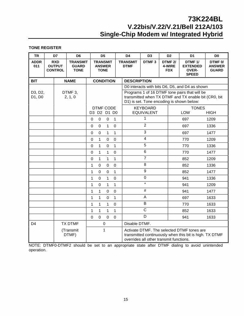
TONE REGISTER
TR D7 D6 D5 D4 D3 D2 D1 D0ADDR
011RXD
OUTPUTCONTROL
TRANSMITGUARDTONE
TRANSMITANSWER
TONE
TRANSMITDTMF
DTMF 3 DTMF 2/4-WIRE
FDX
DTMF 1/EXTENDED
OVER-SPEED
DTMF 0/ANSWERGUARD
BIT NAME CONDITION DESCRIPTIOND6 D5 D4 D0 D0 interacts with bits D6, D5, and D4 as shown
D0 DTMF 0/ X X 1 X Transmit DTMF tones must be in DPSK or Bell 103mode.
Answer/Guard Tone
X 1 0 0 Select Bell mode answer tone. Interacts with DR bit D2and TR bit D5.
X 1 0 1 Select CCITT mode answer tone. Interacts with DR bitD2 and TR bit D5.
1 0 0 0 Select 1800 Hz guard tone.1 0 0 1 Select 550 Hz guard tone.
D4 D1 D1 interacts with D4 as shown.D1 DTMF 1/ 0 0 Asynchronous QAM or DPSK +1% -2.5%. (normal)
ExtendedOverspeed
0 1 Asynchronous QAM or DPSK +2.3% -2.5%. (extendedoverspeed)
D4 D2D2 DTMF 2/ 0 0 Selects 2-wire duplex or half duplex
4 Wire FDX 0 1 D2 selects 4-wire full duplex in the modulation modeselected. The receive path corresponds to the receivemode selected by the ANS/ORIG bit CR0 D0 in terms ofhigh or low band selection. The transmitter is in the sameband as the receiver, but does not have magnitudefiltering or equalization on its signal as in the receivepath.
73K224BLV.22bis/V.22/V.21/Bell 212A/103
Single-Chip Modem w/ Integrated Hybrid
15
TONE REGISTER
TR D7 D6 D5 D4 D3 D2 D1 D0ADDR
011RXD
OUTPUTCONTROL
TRANSMITGUARDTONE
TRANSMITANSWER
TONE
TRANSMITDTMF
DTMF 3 DTMF 2/4-WIRE
FDX
DTMF 1/EXTENDED
OVER-SPEED
DTMF 0/ANSWERGUARD
BIT NAME CONDITION DESCRIPTIOND0 interacts with bits D6, D5, and D4 as shown
D3, D2,D1, D0
DTMF 3,2, 1, 0
Programs 1 of 16 DTMF tone pairs that will betransmitted when TX DTMF and TX enable bit (CR0, bitD1) is set. Tone encoding is shown below:
DTMF CODED3 D2 D1 D0
KEYBOARDEQUIVALENT
TONESLOW HIGH
0 0 0 1 1 697 1209
0 0 1 0 2 697 1336
0 0 1 1 3 697 14770 1 0 0 4 770 12090 1 0 1 5 770 13360 1 1 0 6 770 14770 1 1 1 7 852 12091 0 0 0 8 852 13361 0 0 1 9 852 14771 0 1 0 0 941 13361 0 1 1 * 941 12091 1 0 0 # 941 14771 1 0 1 A 697 16331 1 1 0 B 770 16331 1 1 1 C 852 16330 0 0 0 D 941 1633
D4 TX DTMF 0 Disable DTMF.(TransmitDTMF)
1 Activate DTMF. The selected DTMF tones aretransmitted continuously when this bit is high. TX DTMFoverrides all other transmit functions.
NOTE: DTMF0-DTMF2 should be set to an appropriate state after DTMF dialing to avoid unintendedoperation.

73K224BLV.22bis/V.22/V.21/Bell 212A/103Single-Chip Modem w/ Integrated Hybrid
16
TONE REGISTER (continued)
TR D7 D6 D5 D4 D3 D2 D1 D0ADDR
011RXD
OUTPUTCONTROL
TRANSMITGUARDTONE
TRANSMITANSWER
TONE
TRANSMITDTMF
DTMF 3 DTMF 2/4-WIRE
FDX
DTMF 1/EXTENDED
OVER-SPEED
DTMF 0/ANSWERGUARD
BIT NAME CONDITION DESCRIPTIOND5 D4 D0 D5 interacts with bits D4 and D0 as shown. Also interacts
with DR bit D2 in originate mode (see Detect Registerdescription).
D5 Transmit 0 0 X Disables answer tone generator.Answer Tone 1 0 0 In answer mode, a Bell 2225 Hz tone is transmitted
continuously when the transmit enable bit is set.1 0 1 Likewise, a CCITT 2100 Hz answer tone is transmitted.
D6 Transmit 0 Disables guard tone generator.Guard Tone 1 Enables guard tone generator (see D0 for selection of
guard tones). Bit D4 must be zero.D7 RXD Output 0 Enables RXD pin. Receive data will be output on RXD.
Control 1 Disables RXD pin. The RXD pin reverts to a highimpedance with internal weak pull-up resistor.

73K224BLV.22bis/V.22/V.21/Bell 212A/103
Single-Chip Modem w/ Integrated Hybrid
17
CONTROL REGISTER 2
CR2 D7 D6 D5 D4 D3 D2 D1 D0ADDR
1000 SPEC REG
ACCESSCALL INIT TRANSMIT S1 16 WAY RESETRESETRESETRESET
DSPDSPDSPDSPTRAIN
INHIBITEQUALIZER
ENABLE
BIT NAME CONDITION DESCRIPTIOND0 Equalizer 0 The adaptive equalizer is in its initialized state.
Enable 1 The adaptive equalizer is enabled. This bit is used inhandshakes to control when the equalizer shouldcalculate its coefficients.
D1 Train Inhibit 0 The adaptive equalizer is active.1 The adaptive equalizer coefficients are frozen.
D2 RESET DSP 0 The DSP is inactive and all variables are initialized.
1 The DSP is running based on the mode set by othercontrol bits.
D3 16 Way 0 The receiver and transmitter are using the same decisionplane (based on the modulator control mode).
1 The receiver, independent of the transmitter, is forcedinto a 16 point decision plane. Used for QAMhandshaking.
D4 Transmit S1 0 The transmitter when placed in alternating mark/spacemode transmits 0101...... scrambled or not dependent onthe bypass scrambler bit.
1 When this bit is 1 and only when the transmitter is placedin alternating mark/space mode by CR1 bits D7, D6, andin DPSK or QAM, an unscrambled repetitive double di-bitpattern of 00 and 11 at 1200 bit/s (S1) is sent.
D5 Call Init 0 The DSP is set-up to do demodulation and patterndetection based on the various mode bits. Both answertones are detected in demodulation mode concurrently;TR-D0 is ignored.
1 The DSP decodes unscrambled mark, answer tone andcall progress tones.
0 Normal CR3 access.D6 SpecialRegisterAccess
1 Setting this bit and addressing CR3 allows access to thespecial register (see the special register for details).
D7 Not used at this time 0 Only write zero to this bit.
RESETRESETRESETRESETDSPDSPDSPDSP

73K224BLV.22bis/V.22/V.21/Bell 212A/103Single-Chip Modem w/ Integrated Hybrid
18
CONTROL REGISTER 3
CR3 D7 D6 D5 D4 D3 D2 D1 D0ADDR
101TXDALT TRI-STATE
TX/RXCLKOH RECEIVE
BOOSTENABLE
TRANSMITATTEN. 3
TRANSMITATEN 2
TRANSMITATTEN. 1
TRANSMITATTEN. 0
BIT NAME CONDITION DESCRIPTIOND3 D2 D1 D0
D3, D2,D1,D0
TransmitAttenuator
0 0 0 01 1 1 1
Sets the attenuation level of the transmitted signal in 1dB steps. The default (D3 - D0 = 0100) is for a transmitlevel of -10 dBm0 on the line with the recommendedhybrid transmit gain. The total range is 16 dB.
D4 Receive Gain 0 18 dB receive front end boost is not used.Boost 1 Boost is in the path. This boost does not change
reference levels. It is used to extend dynamic range bycompensating for internally generated noise whenreceiving weak signals. The receive level detect signaland knowledge of the hybrid and transmit attenuatorsetting will determine when boost should be enabled.
D5 OH 0 Relay driver open.1 Open drain driver pulling low.
D6 Tri-state 0 TXCLK and RXCLK are driven.TXCLK/RXCLK 1 TXCLK and RXCLK are tri-stated.
D7 TXDALT Special RegisterBit D3=1
Alternate TX data source (see Special Register).

73K224BLV.22bis/V.22/V.21/Bell 212A/103
Single-Chip Modem w/ Integrated Hybrid
19
SPECIAL REGISTER
SR D7 D6 D5 D4 D3 D2 D1 D0ADDR
1010 TXBAUD
CLOCKRXUN-DSCRDATA
0 TXDSOURCE
SIGNALQUALITY
LEVELSELECT 1
SIGNALQUALITY
LEVELSELECT 0
0
BIT NAME DESCRIPTIOND7, D4, D0 Not used at this time. Only write zeros to these bits.D6 TXBAUD CLK TXBAUD clock is the transmit baud-synchronous clock that can be used to
synchronize the input of arbitrary quad/di-bit patterns. The rising edge ofTXBAUD signals the latching of a baud-worth of data internally. Synchronousdata to be entered via the TXDALT bit, CR3 bit D7, should have datatransitions that start 1/2 bit period delayed from the TXBAUD clock edges.
D5 RXUNDSCRData
This bit outputs the data received before going to the descrambler.This is useful for sending special unscrambled patterns that can be used forsignaling.
D3 TXD Source This bit selects the transmit data source; either the TXD pin if zero or theTXDALT if this bit is a one. The transmit pattern bits D7 and D6 in CR1override either of these sources.
D2, D1 Signal QualityLevel Select
The signal quality indicator is a logical zero when the signal received isacceptable for low error rate reception. It is determined by the value of themean squared error (MSE) calculated in the decisioning process whencompared to a given threshold. This threshold can be set to four levels oferror rate. The SQI bit will be low for good or average connections. As theerror rate crosses the threshold setting, the SQI bit will toggle at a 1.66 msrate. Toggling will continue until the error rate indicates that the data pumphas lost convergence and a retrain is required. At that point the SQI bit will bea one constantly. The SQI bit and threshold selection are valid for QAM andDPSK only and indicates typical error rate.
D2 D1 THRESHOLD VALUE UNITS0 0 10-5 BER (default)0 1 10-6 BER1 0 10-4 BER1 1 10-3 BER
NOTE: This register is "mapped" and is accessed by setting CR2 bit D6 to a one and addressing CR3. Thisregister provides functions to the 73K224BL user that are not necessary in normal communications.Bits D7-D4 are read only, while D3-D0 are read/write. To return to normal CR3 access, CR2 bit D6must be returned to a zero.

73K224BLV.22bis/V.22/V.21/Bell 212A/103Single-Chip Modem w/ Integrated Hybrid
20
ID REGISTER
ID D7 D6 D5 D4 D3 D2 D1 D0ADDR
110ID ID ID ID X X X X
BIT NAME CONDITION DESCRIPTIOND7 D6 D5 D4 Indicates Device:0 0 X X 73K212L, 73K321L or 73K322L0 1 X X 73K221L or 73K302L1 0 X X 73K222L or 73K222BL1 1 0 0 73K224L, 73K224BL
D7, D6,D5, D4
1 1 1 0 73K324L, 73K324BL
73K224BLV.22bis/V.22/V.21/Bell 212A/103
Single-Chip Modem w/ Integrated Hybrid
21
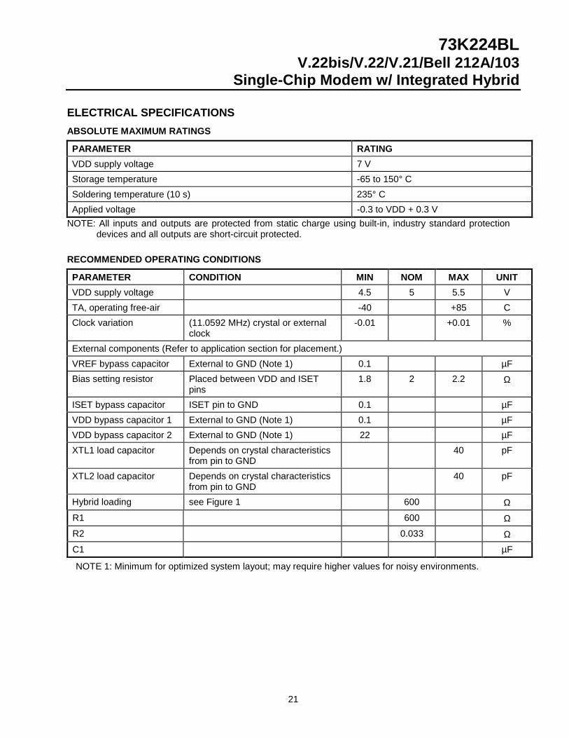
ELECTRICAL SPECIFICATIONSABSOLUTE MAXIMUM RATINGS
PARAMETER RATINGVDD supply voltage 7 VStorage temperature -65 to 150° CSoldering temperature (10 s) 235° CApplied voltage -0.3 to VDD + 0.3 V
NOTE: All inputs and outputs are protected from static charge using built-in, industry standard protectiondevices and all outputs are short-circuit protected.
RECOMMENDED OPERATING CONDITIONS
PARAMETER CONDITION MIN NOM MAX UNITVDD supply voltage 4.5 5 5.5 VTA, operating free-air -40 +85 CClock variation (11.0592 MHz) crystal or external
clock-0.01 +0.01 %
External components (Refer to application section for placement.)VREF bypass capacitor External to GND (Note 1) 0.1 µFBias setting resistor Placed between VDD and ISET
pins1.8 2 2.2 Ω
ISET bypass capacitor ISET pin to GND 0.1 µFVDD bypass capacitor 1 External to GND (Note 1) 0.1 µFVDD bypass capacitor 2 External to GND (Note 1) 22 µFXTL1 load capacitor Depends on crystal characteristics
from pin to GND40 pF
XTL2 load capacitor Depends on crystal characteristicsfrom pin to GND
40 pF
Hybrid loading see Figure 1 600 Ω
R1 600 ΩR2 0.033 ΩC1 µF
NOTE 1: Minimum for optimized system layout; may require higher values for noisy environments.
73K224BLV.22bis/V.22/V.21/Bell 212A/103Single-Chip Modem w/ Integrated Hybrid
22
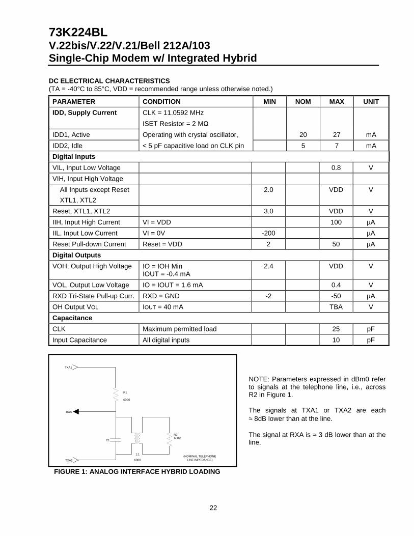
DC ELECTRICAL CHARACTERISTICS(TA = -40°C to 85°C, VDD = recommended range unless otherwise noted.)
PARAMETER CONDITION MIN NOM MAX UNITIDD, Supply Current CLK = 11.0592 MHz
ISET Resistor = 2 MΩ
IDD1, Active Operating with crystal oscillator, 20 27 mAIDD2, Idle < 5 pF capacitive load on CLK pin 5 7 mADigital InputsVIL, Input Low Voltage 0.8 VVIH, Input High Voltage All Inputs except Reset XTL1, XTL2
2.0 VDD V
Reset, XTL1, XTL2 3.0 VDD VIIH, Input High Current VI = VDD 100 µAIIL, Input Low Current VI = 0V -200 µAReset Pull-down Current Reset = VDD 2 50 µADigital OutputsVOH, Output High Voltage IO = IOH Min
IOUT = -0.4 mA2.4 VDD V
VOL, Output Low Voltage IO = IOUT = 1.6 mA 0.4 VRXD Tri-State Pull-up Curr. RXD = GND -2 -50 µAOH Output VOL IOUT = 40 mA TBA VCapacitanceCLK Maximum permitted load 25 pFInput Capacitance All digital inputs 10 pF
FIGURE 1: ANALOG INTERFACE HYBRID LOADING
TXA1
TXA2
RXA
R1
600Ω
600Ω
1:1
R2600Ω
(NOMINAL TELEPHONELINE IMPEDANCE)
C1
NOTE: Parameters expressed in dBm0 referto signals at the telephone line, i.e., acrossR2 in Figure 1.
The signals at TXA1 or TXA2 are each≈ 8dB lower than at the line.
The signal at RXA is ≈ 3 dB lower than at theline.

73K224BLV.22bis/V.22/V.21/Bell 212A/103
Single-Chip Modem w/ Integrated Hybrid
23
ELECTRICAL SPECIFICATIONS (continued)
DYNAMIC CHARACTERISTICS AND TIMING(TA = -40°C to +85°C, VDD = recommended range unless otherwise noted.)
PARAMETER CONDITION MIN NOM MAX UNITQAM/DPSK ModulatorCarrier suppression Measured at TXA 35 dBOutput Amplitude TX Scrambled marks
ATT = 0100 (default)-11.5 -10 -9 dBm0
FSK Modulator/DemodulatorOutput Frequency Error CLK = 11.0592 MHz -0.31 +0.20 %Transmit Level ATT = 0100 (default)
transmit dotting pattern-11.5 -10 -9 dBm0
TXA output distortion All products through BPF -45 dBOutput bias distortion@ RXD
Dotting pattern measured at RXDreceive level -20 dBm, SNR 20 dB
-10 +10 %
Output jitter @ RXD Integrated for 5 seconds -15 +15 %Sum of bias distortion andoutput jitter
Integrated for 5 seconds -17 +17 %
Answer Tone Generator (2100 or 2225 Hz)Output amplitude ATT = 0100 (default level) -11.5 -10 -9 dBm0
Not in V.21Output Distortion Distortion products in receive band -40 dBDTMF Generator Not in V.21Frequency accuracy -0.03 +0.25 %Output amplitude Low band, ATT = 0100, DPSK mode -10 -8 dBm0Output amplitude High band, ATT = 0100, DPSK mode -8 -6 dBm0Twist High band to low band, DPSK mode 1 2 3 dBReceiver Dynamic Range Refer to performance curves -43 -3 dBm0Call Progress Detector In call init modeDetect level 460 Hz test signal -34 0 dBm0Reject level 460 Hz test signal -40 dBm0Delay time -70 dBm0 to -30 dBm0 step 25 msHold time -30 dBm0 to -70 dBm0 step 25 ms

73K224BLV.22bis/V.22/V.21/Bell 212A/103Single-Chip Modem w/ Integrated Hybrid
24
DYNAMIC CHARACTERISTICS AND TIMING (continued)
PARAMETER CONDITION MIN NOM MAX UNITCarrier Detect Receive gain = On for lower input level measurementsThreshold All modes -48 -43 dBm0Hysteresis All modes 2Delay Time FSK 70 dBm0 to -6 dBm0 Change at input 25 37 ms
70 dBm0 to -40 dBm0 Change at input 25 37 msDPSK -70 dBm0 to -6 dBm0 Change at input 7 17 ms
-70 dBm0 to -40 dBm0 Change at input 7 17 msQAM -70 dBm0 to -6 dBm0 Change at input 25 37 ms
-70 dBm0 to -40 dBm0 Change at input 25 37 msHold Time FSK -6 dBm0 to -70 dBm0 Change at input 25 37 ms
40 dBm0 to -70 dBm0 Change at input 15 30 msDPSK -6 dBm0 to -70 dBm0 Change at input 20 29 ms
-40 dBm0 to -70 dBm0 Change at input 14 21 msQAM -6 dBm0 to -70 dBm0 Change at input 25 32 ms
-40 dBm0 to -70 dBm0 Change at input 18 28 msAnswer Tone Detectors DPSK ModeDetect Level -48 -43 dBm0Detect Time Call init mode, 2100 or 2225 Hz 6 50 msHold Time Call init mode, 2100 or 2225 Hz 6 50 msPattern Detectors DPSK ModeS1 Pattern
Delay Time For signals from -6 to -40 dBm0, 10 55 msHold Time Demodulation mode 10 45 ms
Unscrambled MarkDelay Time For signals from -6 to -40 call init 10 45 msHold Time mode 10 45 ms
Receive Level IndicatorDetect On -22 -28 dBm0Valid after Carrier Detect DPSK Mode 1 4 7 ms

73K224BLV.22bis/V.22/V.21/Bell 212A/103
Single-Chip Modem w/ Integrated Hybrid
25
DYNAMIC CHARACTERISTICS AND TIMING (continued)
PARAMETER CONDITION MIN NOM MAX UNITTransmit AttenuatorRange of Transmit Level 1111-0000 (Default ATT=0100) -22 -6 dBm0Step Accuracy -0.15 +0.15 dBClock Noise
TXA pins; 153.6 kHz 1.5 mVrmsCarrier OffsetCapture Range Originate or Answer ±5 HzRecovered ClockCapture Range % of frequency (originate or
answer)-0.02 +0.02 %
Guard Tone GeneratorTone Accuracy 550 Hz +1.2 %
1800 Hz -0.8Tone Level 550 Hz -4.5 -3.0 -1.5 dB(Below QAM/DPSK Output) 1800 Hz -7.5 -6.1 -4.5 dBHarmonic Distortion 550 Hz -50 dB(700 to 2900 Hz) 1800 Hz -50 dB
73K224BLV.22bis/V.22/V.21/Bell 212A/103Single-Chip Modem w/ Integrated Hybrid
26
DYNAMIC CHARACTERISTICS AND TIMING (continued)
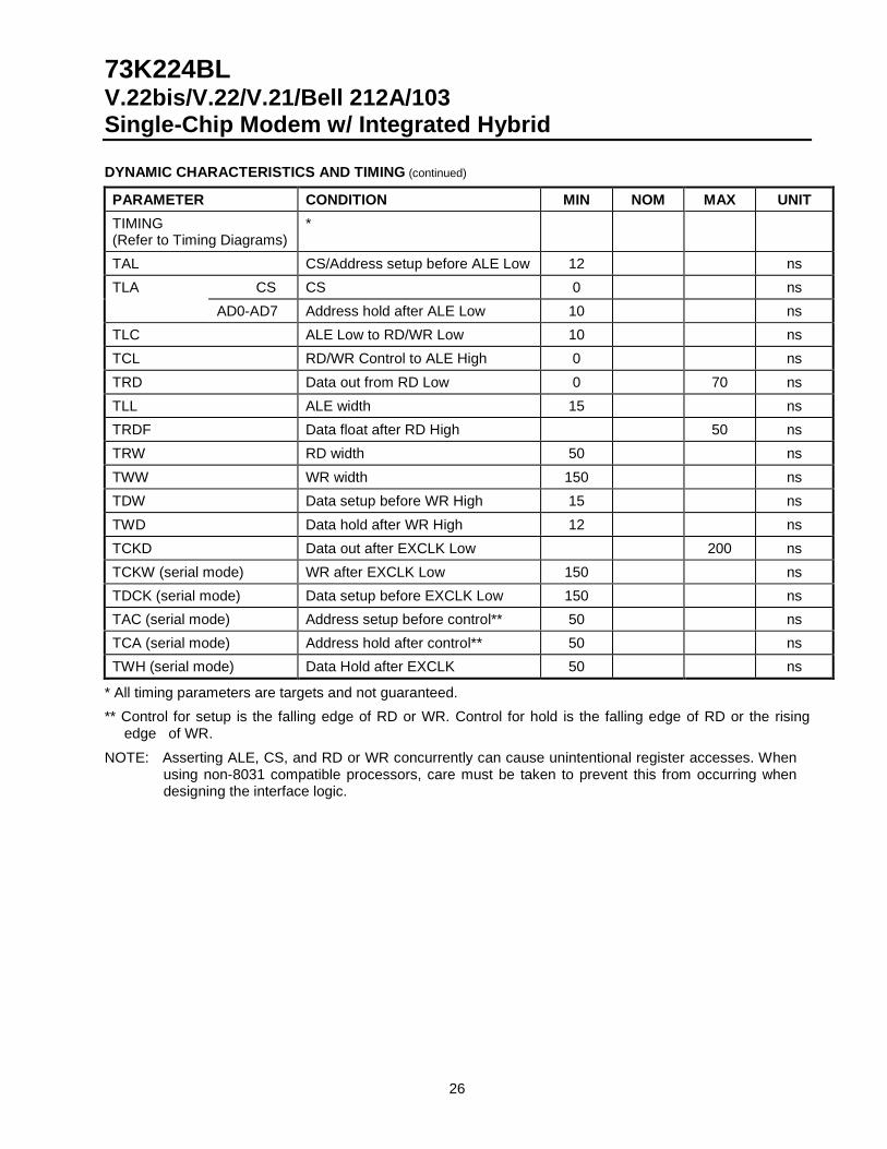
PARAMETER CONDITION MIN NOM MAX UNITTIMING(Refer to Timing Diagrams)
*
TAL CS/Address setup before ALE Low 12 nsTLA CS CS 0 ns
AD0-AD7 Address hold after ALE Low 10 nsTLC ALE Low to RD/WR Low 10 nsTCL RD/WR Control to ALE High 0 nsTRD Data out from RD Low 0 70 nsTLL ALE width 15 nsTRDF Data float after RD High 50 nsTRW RD width 50 nsTWW WR width 150 nsTDW Data setup before WR High 15 nsTWD Data hold after WR High 12 nsTCKD Data out after EXCLK Low 200 nsTCKW (serial mode) WR after EXCLK Low 150 nsTDCK (serial mode) Data setup before EXCLK Low 150 nsTAC (serial mode) Address setup before control** 50 nsTCA (serial mode) Address hold after control** 50 nsTWH (serial mode) Data Hold after EXCLK 50 ns
* All timing parameters are targets and not guaranteed.** Control for setup is the falling edge of RD or WR. Control for hold is the falling edge of RD or the rising
edge of WR.NOTE: Asserting ALE, CS, and RD or WR concurrently can cause unintentional register accesses. When
using non-8031 compatible processors, care must be taken to prevent this from occurring whendesigning the interface logic.

73K224BLV.22bis/V.22/V.21/Bell 212A/103
Single-Chip Modem w/ Integrated Hybrid
27
TIMING DIAGRAMS
ALE
TLL
TLC TRW TCL
TLC TWW
ADDRESS ADDRESSREAD DATA WRITE DATA
TDWTALTLA TRD TRDF
AD0-AD7
RD
WR
CS
TWD
FIGURE 2: Bus Timing Diagram (Parallel Control Mode)
ADDRESS
TACTCA
TRD TCKD TRDF
D0 D1 D2 D3 D4 D5 D6 D7
EXCLK
RD
AD0-AD2
DATA
FIGURE 3: Read Timing Diagram (Serial Control Mode)
EXCLK
WR
AD0-AD2 ADDRESS
DATA
TDCK
D0 D1 D2 D3 D4 D5 D6 D7
TCKW
TWW
TAC TCA
TWH
FIGURE 4: Write Timing Diagram (Serial Control Mode)

73K224BLV.22bis/V.22/V.21/Bell 212A/103Single-Chip Modem w/ Integrated Hybrid
28
APPLICATIONS INFORMATIONGENERAL CONSIDERATIONSFigure 5 shows the basic circuit diagram for a73K224BL modem integrated circuit designed tobe used in conjunction with a control processor, aUART or RS-232 serial data interface, and a DAAphone line interface to function as a typicalintelligent modem. The K-Series ICs interfacedirectly with Intel 8048 and 80C51microprocessors for control and status monitoringpurposes. A typical DAA arrangement is shown inFigure 5. This diagram is for reference only anddoes not represent a production-ready modemdesign.The 73K224BL is available with two controlinterface versions: one for a parallel multiplexed
address/data interface, and one for a serialinterface. The parallel version is intended for usewith 8039/48 or 8031/51 compatiblemicrocontrollers from Intel or many othermanufacturers. The serial interface mode can beused with other microcontrollers or in applicationswhere only a limited number of port lines areavailable or the application does not lend itself to amultiplexed address/data interface. The parallelversions may also be used in the serial mode, asexplained in the data sheet pin description.In most applications the controller will monitor theserial data for commands from the DTE and thereceived data for break signals from the far endmodem. In this way, commands to the modem aresent over the same line as the transmitted data. Inother applications the RS-232 interface handshakelines are used for modem control.
RING DETECT
TX DATARX DATA
11.0592
ADR/DATA BUS
µC ALEµC WR
µC RD
RXCLKTXCLKEXCLKCHIP SELECT
CONTROLINTERFACE
10 µF 0.1 µF
+
+5
+5
2 MΩ1 µF
0.1 µF
0.1 µF
8.2 K
600 Ω+5
0.033 µFTYP.
600 Ω1:1
HOOKRELAY
RINGDETECTOR
TRANSIENTSUPPRESSOR
FUSE
RJ - 11
1234
123456789
10111213141516 17
181920212223242526272829303132GND
CLKXTL1XTL2AD0
AD3
AD1AD2
AD4AD5AD6AD7ALEWRRD
VDD
RXAVREF
RESETN/C
ISET
RXD
OH
RXCLK
TXDCS
EXCLKTXCLK
INT
N/CTXA1TXA2
TRANSFORMER
+
FIGURE 5: Typical 73K224BL DAA Circuit

73K224BLV.22bis/V.22/V.21/Bell 212A/103
Single-Chip Modem w/ Integrated Hybrid
29
APPLICATIONS INFORMATION (continued)
DIRECT ACCESS ARRANGEMENT (DAA)The DAA (Direct Access Arrangement) requiredfor the 73K224BL consists of an impedancematching resistor, telecom coupling transformer,and ring detection and fault protection circuitry.The transformer specifications must comply withthe impedance of the country in which the modemis being operated. Transformers designedspecifically for use with the telephone networkshould be used. These may present a DC load tothe network themselves (a “wet” transformer) orthey may require AC coupling with a DC loadprovided by additional devices (a “dry”transformer). A dry transformer will generallyprovide higher performance and smaller size thana wet transformer. A wet transformer allows asimpler design, but must not saturate with theworst case DC current passing through it ordistortion and poor performance will result.The protection circuitry typically consists of atransient suppression device and current limiter toprotect the user and the telephone network fromhazardous voltages that can be present underfault conditions. The transient suppresser may bea MOV (metal oxide varistor), Sidactor (TeccorElectronics Inc.), spark gap device, or avalanchediode. Some devices clamp the transient to theirspecified break down voltage and others go intolow impedance crowbar state. The latter requirethat the fault current cease before they can returnto their inactive state.Current limiting devices can consist of a resistor,Raychem PolySwitch resettable fuse, or slowblow fuse that can withstand the transient testswithout permanent damage or replacement.Ring detection circuitry is not required by the FCC,but may be required by the application. The ringdetector usually consists of an optoisolator,capacitor, and resistor to present the proper ACload to the network to meet the REN (RingEquivalency Number) regulations of FCC Part 68.The K-Series Design Manual contains detailedinformation on the design of a ring detect circuitsas well as the other topics concerning the DAA.
DESIGN CONSIDERATIONSSemiconductor's one-chip modem productsinclude all basic modem functions. This makesthese devices adaptable for use in a variety ofapplications, and as easy to control asconventional digital bus peripherals.Unlike digital logic circuitry, modem designs mustproperly contend with precise frequencytolerances and very low level analog signals, toensure acceptable performance. Using goodanalog circuit design practices will generally resultin a sound design. Following are additionalrecommendations which should be taken intoconsideration when starting new designs.
CRYSTAL OSCILLATORThe K-Series crystal oscillator requires a parallelmode (anti-resonant) crystal which operates at11.0592 MHz. It is important that this frequency bemaintained to within ±0.01% accuracy.In order for a parallel mode crystal to operatecorrectly and to specification, it must have acapacitor connected to the junction of each of thecrystal and internal inverter connections,terminated to ground. The values of thesecapacitors depend primarily on the crystal’scharacteristics, and to a lesser degree on theinternal inverter circuit. The values used affect theaccuracy and start up characteristics of theoscillator.
LAYOUT CONSIDERATIONSGood analog/digital design rules must be used tocontrol system noise in order to obtain highestperformance in modem designs. The more digitalcircuitry present on the PC board, the more thisattention to noise control is needed. The modemshould be treated as a high performance analogdevice. A 22 µF electrolytic capacitor in parallelwith a 0.1 µF ceramic capacitor between VDD andGND is recommended. Liberal use of groundplanes and larger traces on power and ground arealso highly favored. High speed digital circuits tendto generate a significant amount of EMI (Electro-Magnetic Interference) which must be minimizedin order to meet regulatory agency limitations. Toaccomplish this, high speed digital devices shouldbe locally bypassed, and the telephone lineinterface and K-Series device should be located
73K224BLV.22bis/V.22/V.21/Bell 212A/103Single-Chip Modem w/ Integrated Hybrid
30
close to each other near the area of the boardwhere the phone line connection is accessed. Toavoid problems, power supply and ground tracesshould be routed separately to the analog anddigital functions on the board, and digital signalsshould not be routed near low level or highimpedance analog traces. The analog and digitalgrounds should only connect at one point near theK-Series device ground pin to avoid ground loops.The K-Series modem ICs should have both highfrequency and low frequency bypassing as closeto the package as possible.
MODEM PERFORMANCECHARACTERISTICSThe curves presented here define modem ICperformance under a variety of line conditionswhile inducing disturbances that are typical ofthose encountered during data transmission onpublic service telephone lines. Test data wastaken using an AEA Electronics’ “Autotest I”modem test set and line simulator, operatingunder computer control. All tests were run full-duplex, using a Concord Data Systems 224 as thereference modem. A 511 pseudo-random-bitpattern was used for each data point. Noise wasC-message weighted and all signal-to-noise (S/N)ratios reflect total power measurements similar tothe CCITT V.56 measurement specification. Theindividual tests are defined as follows.
BER VS. S/NThis test measures the ability of the modem tooperate over noisy lines with a minimum of data-transfer errors. Since some noise is generated inthe best of dial-up lines, the modem must operatewith the lowest S/N ratio possible. Better modemperformance is indicated by test curves that areclosest to the BER axis. A narrow spread betweencurves representing the four line parametersindicates minimal variation in performance whileoperating over a range of operating conditions.Typically, a DPSK modem will exhibit better BERperformance test curves receiving in the low bandthan in the high band.
BER VS. RECEIVE LEVELThis test measures the dynamic range of themodem. Because signal levels vary widely overdial-up lines, the widest possible dynamic range isdesirable. The minimum Bell specification calls for36 dB of dynamic range. S/N ratios are heldconstant at the indicated values while the receivelevel is lowered from a very high to very low signallevels. The width of the “bowl” of these curves,taken at the BER point, is the measure of dynamicrange.

73K224BLV.22bis/V.22/V.21/Bell 212A/103
Single-Chip Modem w/ Integrated Hybrid
31
4 6 8 10 12 14 16
SIGNAL TO NOISE (dB)
BIT
ERR
OR
RAT
E
10 -6
10 -5
10 -4
10 -3
10 -2
3002
LOW BAND RECEIVE-30 dBm
DPSK OPERATION1200 BIT/S
C1, C2, FLAT
4 6 8 10 12 14 16
SIGNAL TO NOISE (dB)
BIT
ERR
OR
RAT
E
10 -6
10 -5
10 -4
10 -3
10 -2
C1, 3002, FLAT
HIGH BAND RECEIVE-30 dBm
DPSK OPERATION1200 BIT/S
C2
8 10 12 14 16 18 20
SIGNAL TO NOISE (dB)
BIT
ERR
OR
RAT
E
10 -6
10 -5
10 -4
10 -3
10 -2
HIGH BAND RECEIVE-30 dBm
QAM OPERATION2400 BIT/S
C1
FLAT
3002
C2
8 10 12 14 16 18 20
SIGNAL TO NOISE (dB)
BIT
ERR
OR
RAT
E
10 -6
10 -5
10-4
10-3
10-2
HIGH BAND RECEIVE-30 dBm
QAM OPERATION2400 BIT/S
C1
FLAT
3002
C2
73K224BL BER vs S/N-DPSK LOW BAND 73K224BL BER vs S/N-DPSK HIGH BAND
73K224BLBER VS S/N-QAM-LOW BAND
73K224BLBER VS S/N-QAM-HIGH BAND

73K224BLV.22bis/V.22/V.21/Bell 212A/103Single-Chip Modem w/ Integrated Hybrid
32
MECHANICAL SPECIFICATIONS
32-Lead PLCC
PIN NO. 1 IDENT.
0.595 (15.11)0.585 (14.86)
0.453 (11.51)0.449 (11.40)
0.553 (14.05)
0.549 (13.94)
0.0230.029
0.045 (1.140)0.020 (0.508)
0.050
0.013 0.021
0.026 0.032
0.495 (12.57)0.485 (12.32)
0.430 (10.92)0.390 (9.91)
0.530 (13.46)0.490 (12.45)
0.300 REF(7.62 REF)
0.400 REF(10.16 REF)
0.095 (2.41)
0.078 (1.98)
0.140 (3.56)0.123 (3.12)
44-Lead TQFP
0.42 (0.0165) Typ.
INDEX
1
16.0 BSC (0.630)
16.0
BS
C (
0.63
0)
1.35 (0.053)1.45 (0.057)
1.00 (0.0394) Typ.
14.0 BSC (0.552)
0.09 (0.035)0.20 (0.008)
0.60 (0.024) Typ.

73K224BLV.22bis/V.22/V.21/Bell 212A/103
Single-Chip Modem w/ Integrated Hybrid
33
PACKAGE PIN DESIGNATIONS(Top View)
AD0
AD1
AD2
AD3
AD4
AD5
AD6
DATA/AD7
ALE
XTAL
2
XTAL
1
CLK
GN
D
RXA
VREF
RES
ET
N/C
ISET
OH
RXCLK
RXD
TXD
CS
EXCLK
TXCLK
WR
RD
VDD
TXA2
TXA1 N/C INT
4 3 2 1 32 31 305
6
7
8
9
10
11
12
13
29
28
27
26
25
24
23
22
2114 15 16 17 18 19 20
32-Lead PLCC 44-Lead TQFP73K224BL-IH 73K224BL-IGT
ORDERING INFORMATIONPART DESCRIPTION ORDER NUMBER PACKAGING MARK73K224BL 32-Lead PLCC 73K224BL-IH 73K224BL-IH73K224BL 44-Lead TQFP 73K224BL-IGT 73L224BL-IGT
No responsibility is assumed by TDK Semiconductor Corporation for use of this product nor for any infringements of patents andtrademarks or other rights of third parties resulting from its use. No license is granted under any patents, patent rights or trademarks ofTDK Semiconductor Corporation, and the company reserves the right to make changes in specifications at any time without notice.Accordingly, the reader is cautioned to verify that the data sheet is current before placing orders.
TDK Semiconductor Corporation, 2642 Michelle Dr., Tustin, CA 92780-7019, (714) 508-8800, FAX: (714) 508-8877
Protected by the following Patents (4,691,172) (4,777,453)© 1996 - 2000 TDK Semiconductor Corporation 04/24/00 - rev. E
CAUTION: Use handling procedures necessary fora static sensitive component.

This datasheet has been download from:
www.datasheetcatalog.com
Datasheets for electronics components.


