Embed Size (px)
Citation preview

Musical Instrument TunerFinal Project ReportDecember 9, 1999
E157
Rohit Mishra and Mark Wang
Abstract:
Most musicians use special devices to tune their instruments. Tuning devices can be as simple as tuningforks which vibrate at specific frequencies, or more user-friendly devices such as analog strobe tuners ordigital tuners. This project prototypes a digital tuner consisting of a keypad, microcontroller, microphone,and LED display. The user selects the note they wish to tune by pressing a key on the keypad. This noteletter is displayed for the user’s convenience. The user then plays the note into the microphone. Themicrocontroller samples the note played and performs a Fast Fourier Transform (FFT) on it. Themicrocontroller sends the primary frequency of the note to an FPGA, where glue logic determines thesharpness or flatness of the note. The result is indicated on a row of LEDs. This digital tuner performs asexpected within limitations of the implementation.
2
IntroductionBackground:We have constructed a working tuner for use in musical applications. Standard musical convention hasdefined certain frequencies as “notes”. Sharp notes sound at a slightly higher frequency than the standard.Flat notes are slightly lower in frequency. Musicians use audio tuners to tune their instruments properly.Our tuner gives a visual indication of the flatness or sharpness of a played note.
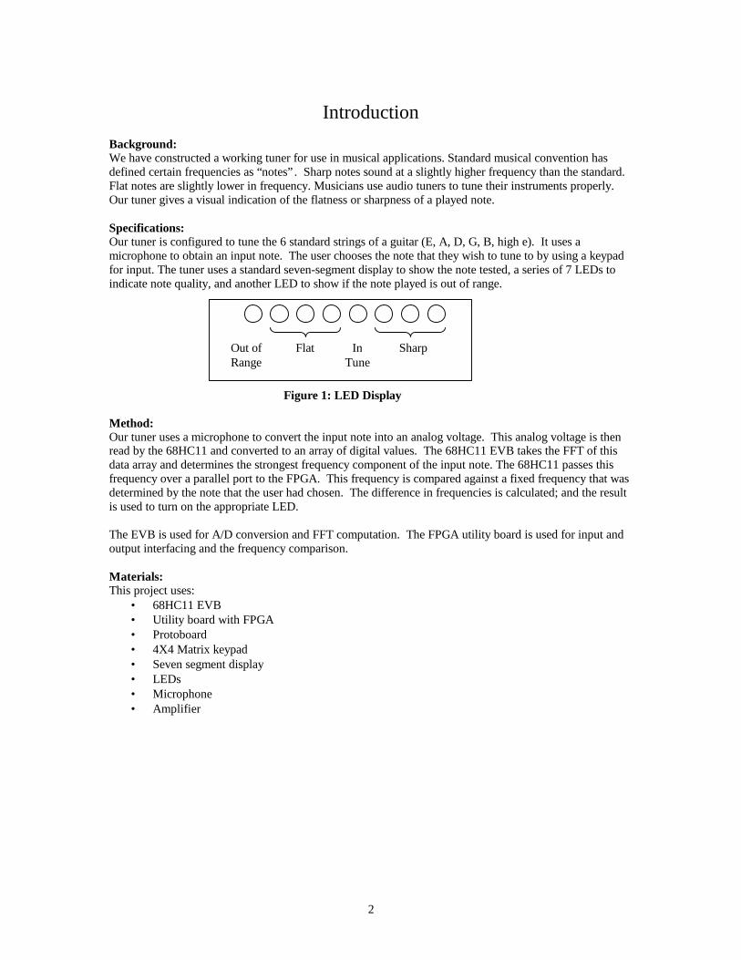
Specifications:Our tuner is configured to tune the 6 standard strings of a guitar (E, A, D, G, B, high e). It uses amicrophone to obtain an input note. The user chooses the note that they wish to tune to by using a keypadfor input. The tuner uses a standard seven-segment display to show the note tested, a series of 7 LEDs toindicate note quality, and another LED to show if the note played is out of range.
Figure 1: LED Display
Method:Our tuner uses a microphone to convert the input note into an analog voltage. This analog voltage is thenread by the 68HC11 and converted to an array of digital values. The 68HC11 EVB takes the FFT of thisdata array and determines the strongest frequency component of the input note. The 68HC11 passes thisfrequency over a parallel port to the FPGA. This frequency is compared against a fixed frequency that wasdetermined by the note that the user had chosen. The difference in frequencies is calculated; and the resultis used to turn on the appropriate LED.
The EVB is used for A/D conversion and FFT computation. The FPGA utility board is used for input andoutput interfacing and the frequency comparison.
Materials:This project uses:
• 68HC11 EVB• Utility board with FPGA• Protoboard• 4X4 Matrix keypad• Seven segment display• LEDs• Microphone• Amplifier
Out of Flat In Sharp Range Tune
3
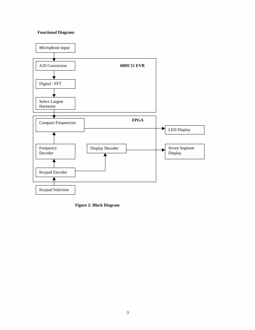
Functional Diagram:
Microphone Input
A/D Conversion
Digital / FFT
Select LargestHarmonic
Keypad Selection
LED Display
Compare Frequencies
Seven SegmentDisplay
68HC11 EVB
FPGA
FrequencyDecoder
Display Decoder
Keypad Encoder
Figure 2: Block Diagram

4
New HardwareMicrophone:The tuner uses a microphone element to acquire an input note. Interfacing the microphone is simple butworth mentioning here in case any future students wish to use a microphone input. Our microphoneinterface consists of two stages. The first is the microphone element itself, and the second is an amplifiercircuit whose output is the input to the tuner system.
Our microphone is a balanced, three-terminal device. Pin 1 takes power, pin 3 is grounded, and the outputsignal is on pin 2. We found that a range of DC voltages can be used to power the microphone. We powerit with 15 VDC through a circuit with two series resistors and a shunt capacitor to ground between them.The resistors are 1 kΩ each, and the capacitor is 100uF/25V (electrolytic). We have chosen thesecomponent values per recommendation from the microphone element manufacturer. The output from pin 2has a DC level of about 0.3 V and swings on the order of a few millivolts.
Because of the small output, we use an inverting op-amp amplifier to boost the microphone output beforesending it to the rest of the tuner system. Because we desire to control the tuner input’s DC offset, we use a0.1uF capacitor at the microphone output to block its 0.3 V offset. This signal then goes to an invertingamplifier constructed with a 411 op-amp and two resistors which control the gain. Our resistor values are750 Ω (at the negative input) and 910 kΩ (in the feedback path). We have arrived at these valuesexperimentally, as they provide an output sufficient for the tuner. +15 and –15 VDC power the op-amp,and its output feeds to the rest of the tuner system.
Future microphone element users can handle the microphone output however they choose to; the importantdetails to remember are that the output has a small DC offset and has a typical amplitude of only a fewmillivolts. Also, experimentation may reveal that the power input to the microphone can be handled withdifferent component values or even a different circuit.
5
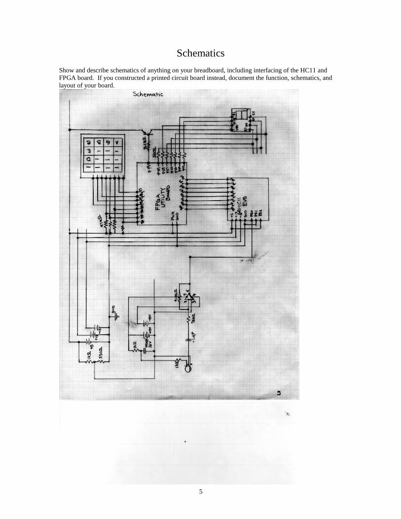
SchematicsShow and describe schematics of anything on your breadboard, including interfacing of the HC11 andFPGA board. If you constructed a printed circuit board instead, document the function, schematics, andlayout of your board.
6
Microcontroller DesignThe microcontroller subsystem of the tuner accepts the user input note, calculates its frequency spectrumusing a FFT, determines the note’s strongest frequency, and sends a representation of this frequency to theFPGA over parallel port B.
A/D Conversion of an Input Signal:The microcontroller input is a signal on channel PE7. This input signal is converted to the digital domainwith A/D reference voltages of +5 V and 0 V. Our A/D conversion routine takes 256 samples at a rate ofabout 1.8 kHz. The value of each sample is written to a byte in memory beginning at $DD00. This datablock, then, occupies addresses $DD00 to $DDFF. The A/D subroutine contains a loop that writes an A/Dresult to memory 256 times. At the beginning of each time through the loop (labeled cklp), the data blockpointer is incremented, and once it equals $DE00, the loop breaks and the A/D is complete. Within thisoverall loop, eight 128 clock cycle loops slow down the effective A/D sampling rate. The maximum A/Dsampling rate with a 2 MHz E clock on the 68HC11 is 62.5 kHz. Reading only one result after acompletion of four conversions reduces the effective sampling rate to 15.625 kHz. Performing A/Dconversions without saving results can further slow this rate. The loops labeled wait1 – wait7 begin with awrite to the A/D control register (at $1030, thus beginning an A/D conversion sequence) and break onlyafter four conversions are complete (indicated by CCF in ADCTL being set). The final “wait” loop alsouses 128 clock cycles by checking the CCF flag, and then the routine proceeds to read an A/D conversionresult from the first result register (ADR1 at $1031). This value is then written to the data block. Dividing15.625 kHz by 8 in addition to extra clock cycles from other instructions in the A/D loop gives us aneffective sampling rate of approximately 1.8 kHz.
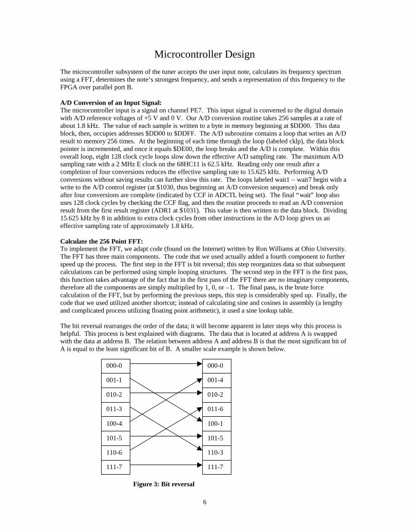
Calculate the 256 Point FFT:To implement the FFT, we adapt code (found on the Internet) written by Ron Williams at Ohio University.The FFT has three main components. The code that we used actually added a fourth component to furtherspeed up the process. The first step in the FFT is bit reversal; this step reorganizes data so that subsequentcalculations can be performed using simple looping structures. The second step in the FFT is the first pass,this function takes advantage of the fact that in the first pass of the FFT there are no imaginary components,therefore all the components are simply multiplied by 1, 0, or –1. The final pass, is the brute forcecalculation of the FFT, but by performing the previous steps, this step is considerably sped up. Finally, thecode that we used utilized another shortcut; instead of calculating sine and cosines in assembly (a lengthyand complicated process utilizing floating point arithmetic), it used a sine lookup table.
The bit reversal rearranges the order of the data; it will become apparent in later steps why this process ishelpful. This process is best explained with diagrams. The data that is located at address A is swappedwith the data at address B. The relation between address A and address B is that the most significant bit ofA is equal to the least significant bit of B. A smaller scale example is shown below.
000-0
001-1
010-2
011-3
100-4
101-5
110-6
111-7
000-0
001-4
010-2
011-6
100-1
101-5
110-3
111-7
Figure 3: Bit reversal

7
Our data set has more elements, but the principle is the same. The data in $DD00 and $DDFF remain inthe same locations, but for instance, data in $DD41 is swapped with the data in $DD82, etc. This is done atlabel revbit. Label rev1 uses a loop to reverse the bits of address one; then it saves the data from addresstwo (the bit reversed address one). Next it stores the value in address one to address two. Finally it storesthe saved data to address one. It continues in this fashion until the entire 256-element array has beenrearranged.
The next step is to sum together the first pass components. In an 8-bit transform the first pass will be onlyin multiples of 180 degrees, and differences of 4 cells apart. It turns out that for any size array that is amultiple of 2; the bit reversal puts the necessary multiples next to each other. So the paired values areadded and subtracted together. The example is continued below.
Figure 4: Calculations after bit reversal
This is done at label fpss. This is a well-commented section. To clarify data one and data two are summedand stored in address one, and data one and data two are subtracted and stored in address two. Then thealgorithm moves on to the next pair. This process is repeated until the entire array has been completed.
After this step, the process must continue as a standard DFT, but again the reordering of the bits is crucial,because it makes the looping process considerably easier. The next step would pair in twos, the pass afterthat would pair off in fours, and the final pass would be the first and eighth cell. Unfortunately, due to thefact that the angles are not “nice”, there are going to be cosines and imaginary sine products. Thiscalculation is helped considerably by the sine lookup table, which is a table of fractional values of 128 toapproximate the sine/cosine function. This function begins at label four to initialize variables, but eachsuccessive pass loops back to label npass. Essentially, npass uses a subroutine smul to multiply the data bytheir respective angle offset cosine and sine. These are then summed and subtracted in the usual methodand then stored in their respective data locations. Each time that npass is done, the data is re-scaled ifnecessary to ensure that there is no overflow.
Unfortunately, implementation of the FFT in assembly is considerably difficult. The algorithm foraddressing can only be done for sample cases less than or equal to 256 (the maximum number of addressesexpressible in a single byte of information). Furthermore since each data address can only hold an integervalue from 0 to 256 which must be converted to two’s complement, the resolution of the data is poor. Thecode utilized a scaling function to ensure that there would be no overflow in data.
Finally, all of these issues combined in an unforeseen bug in the program. The DC offset (the first addressin memory) was very large in our sample data (it required a large offset to protect the ADC circuits in theHC6811). Unfortunately, this left us in a difficult position. If we included the DC offset in the scalingfunction, then the other harmonics would be scaled out rapidly (the DC offset was much stronger than thefundamental frequency of the note). And yet, the DC offset is critical to the FFT function. The solution
000-0
001-4
010-2
011-6
100-1
101-5
110-3
111-7
000-4
001--4
010-8
011--4
100-6
101--4
110-A
111--4
+
-
+
-
+
-
+
-
8
that we came to was to zero out the DC offset position throughout the calculation. Unfortunately, thismade our implementation of the FFT inaccurate, however it was accurate enough to distinguishcharacteristic frequencies. While this is not the most satisfying solution, it did work.
Absolute Value of FFT Results:After the FFT routine stores its data in the data block, we convert it out of two’s compliment form by usingan absolute value subroutine. The subroutine loops 256 times until it has looked at every value in the datablock. Within the loop (labeled all256), the value at the data pointer is AND masked with #$80 todetermine whether it is positive or negative. If it is already positive, the data pointer is incremented and theall256 loop rerun. If the value is negative, its two’s compliment is obtained by flipping its bits with theCOMB instruction and adding one. After rewriting the original value’s absolute value to the memoryblock, the all256 reruns.
This subroutine is not necessary for the program to continue and find the strongest frequency component;however, it allows us to look at a meaningful plot of the FFT result in a graphing program such as Excel.
Find the Strongest Frequency Component:The 68HC11 program uses another subroutine to find the strongest frequency component of the stored FFT.This routine examines only the first 127 data points after the DC component because the 256-point FFT issymmetric. This routine uses a modified version of David Honeycutt’s program from Lab 5 which findsthe largest of 5 numbers stored in consecutive memory locations. Our routine finds the largest of 256values written to consecutive bytes of memory beginning at $DD00, and when it does, saves the value’smemory location to $DDF0. Thus, the strongest frequency position of the FFT relative to DC is saved at$DF01.
Send Strongest Frequency to the FPGA Using Parallel Port B:After finding the strongest frequency position, the 68HC11 program writes this position to parallel port B(at $1004) to send the value to the FPGA board. After sending the data, the program resets the stackpointer to $004A and loops back to obtain another 256 samples and process them. We reset the stackpointer because somewhere in the FFT routine, it increments by 2. Resetting it after each time through theFFT loop ensures the program can run forever.

9
FPGA DesignOur FPGA system handles user input on a keypad, input from the 68HC11 parallel port, and formats outputfor display LEDs. The hardware in the FPGA is similar to that generated for Lab 4. For the tuner, theFPGA performs subtraction and additional encoding.
Display and Frequency Encoding (poll_kb):Whereas in Lab 4 the keypad encoding process converted an 8-bit key press to a 4-bit value for displaydecoding, our FPGA also encodes a valid key press into another 8-bit value. This value is a representationof the standard note frequency to which the frequency position from the 68HC11 is compared.
We determined the frequency values encoded by key presses experimentally by running our FFT routine onsignals with frequencies set by a function generator to standard note frequencies. They expectedly cameout to be close to what we had calculated assuming a 7 Hz spacing between FFT data points. The notefrequencies our tuner tunes to and their associated values in hardware are summarized here:
Note Frequency (Hz) Representation (hex) Representation (decimal)E 164.81 18 23A 220 20 31D 293.66 2B 42G 392 39 56B 493.88 48 71e 659.26 5F 94
Table 1: Note Frequencies
Seven Segment Decoder Module (seven_seg_display):Keypad encodings are modified to display 6 note names on the 7-segment display corresponding to 6 keys,and to display dashes for the other keys (a sign of an invalid key press). The keys on the standard E157keypad display the following:
Key on keypad Letter printed on displayA A0 GB bD dE E (for low E string on a guitar)F e (for high E string on a guitar)All rest -
Table 2: Key presses
10
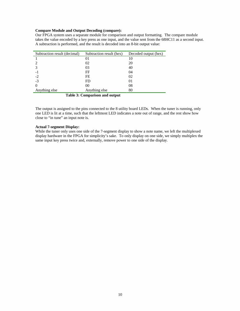
Compare Module and Output Decoding (compare):Our FPGA system uses a separate module for comparison and output formatting. The compare moduletakes the value encoded by a key press as one input, and the value sent from the 68HC11 as a second input.A subtraction is performed, and the result is decoded into an 8-bit output value:
Subtraction result (decimal) Subtraction result (hex) Decoded output (hex)1 01 102 02 203 03 40-1 FF 04-2 FE 02-3 FD 010 00 08Anything else Anything else 80
Table 3: Comparison and output
The output is assigned to the pins connected to the 8 utility board LEDs. When the tuner is running, onlyone LED is lit at a time, such that the leftmost LED indicates a note out of range, and the rest show howclose to “in tune” an input note is.
Actual 7-segment Display:While the tuner only uses one side of the 7-segment display to show a note name, we left the multiplexeddisplay hardware in the FPGA for simplicity’s sake. To only display on one side, we simply multiplex thesame input key press twice and, externally, remove power to one side of the display.

11
ResultsTuner Response to Various Inputs:Our project was successful, however the final product still has some problems. We found that our tunercould successfully tune all 6 notes that we had intended to tune to. The software implementation of thedesign runs an infinite loop, outputting a result approximately every 500 milliseconds. Unfortunately, themicrophone posed a significant problem in analog electronics. The amplifier and microphoneimplementation was designed experimentally. Due to these analog difficulties, the tuner had difficultytuning an actual guitar. We believe this is in part due to the complex waveform, as well as rapid drop off instrength of the guitar’s note. We tried to use a speaker to output a continuous amplitude note, and thetuner’s performance was slightly better, although still not completely reliable. If a signal generator isdirectly hooked up to the A/D converter, then performance is near perfect.
Changes From the Original Proposal:Our initial proposal suggested the usage of 7 LEDs. We thought that the 7 LEDs could give an accurateidea of the sharpness/flatness of the note. An improvement was made later when we added an eighth LEDto show whether or not the frequency that was being played was out of range of the tuner’s ability.Furthermore, for aesthetic appeal, we used different colors for the LEDs. The green center LED indicates“in tune”, the six red LEDs indicate degree of flatness/sharpness. The out of range LED is yellow.
Future Recommendations:Future recommendations for this project are related to increasing the resolution of the tuner. This can bedone in two ways. The first would be to increase the number of points in the FFT (therefore also increasingthe number of A/D samples). If this is done properly, higher resolution is possible; unfortunately, thisapproach requires a new method of addressing. The FFT algorithm that we used can only handle 256different pieces of data because the bit reversal operation depends on byte long addresses. A simplerapproach to this dilemma is to further slow down the A/D conversion. This would end up giving a smallerrange of tuning ability, but it would give better resolution to the frequency peaks. Another possibleimprovement would be an automatic gain control for the microphone. Unfortunately, neither of us knowshow to implement a proper AGC circuit. Finally, it would not take long to make an auto-tuning device; thiscould be implemented using a comparison loop for all of the valid frequencies. Only the frequency that theplayed note is actually closest to would be used for tuning calculations. Finally, our project can tune to anynote within its frequency range, so modifying this tuner to tune a piano or trumpet would not be terriblydifficult.
Comical Side Note:Once we got the guitar back to a commercial tuner, we realized that the guitar was more out of tune than ithad been before we had used our tuner on it.
12
References[1] R. Lord, “Fast Fourier for the 6800.” Byte, February 1979, pp. 108-119.[2] ftp://ftp.stanford.edu/class/ee281/WWW97/routines/ffthc11.asm for FFT code
Parts ListComponents used in the tuner include:
Part Source Vendor Part # PriceMicrophone Element MarVac on Holt Ave. 10-84 $2.79411 Op-Amp Electronics Lab
Table 4: Parts List

Appendices68HC11 ASM code listing:
0001 * - tuner.asm0002 * - A 68HC11 program to continuously sample an0003 * input waveform, obtain its fourier spectrum,0004 * and output frequency information on parallel0005 * port B.0006 * - By Rohit Mishra and Mark Wang0007 * for E157, Harvey Mudd College0008 * - 12/9/990009 *0010 * - One loop of the program runs in several stages.0011 * First, an input is acquired from an A/D channel0012 * on PE7. 256 1-byte samples are taken and stored0013 * memory locations $DD00 - $DDFF.0014 *0015 * Secondly, a 256 point FFT is performed on the0016 * sample space. The FFT algorithm was implemented0017 * by Ron Williams of Ohio University; his comments0018 * appear below.0019 *0020 * After the FFT has been calculated, the location0021 * in memory of the strongest frequency is found.0022 * Its position relative to the DC component of the0023 * FFT is determined and written to parallel port B.0024 *0025 * Before looping back to acquire another input0026 * sample, the stack pointer is reset to a0027 * specific value so as to ensure safe infinite0028 * looping.0029 *0030 * - fast fourier transform for the 68HC110031 * originally written by:0032 *0033 * Ron Williams0034 * Department of Chemistry0035 * Ohio University0036 * Athens, OH 457010037 *0038 * - Excerpts of Ron Williams' comments:0039 * This is a modification of the 6800 FFT presented by:0040 * Richard Lord0041 * Byte Magazine, pp. 108-1190042 * February 19790043 *0044 * My version is written in ROMable code for the HC11.0045 * It uses a sine look-up table for speed and can only0046 * transform 256 8-bit data points. The program0047 * assumes that the address of the real data is pushed0048 * on the stack prior to the call and that a 256 byte0049 * imaginary buffer is at data+256 therefore you must0050 * declare a 512 byte data array in the calling routine0051 * and load the lower 256 bytes with data. The FFT0052 * will zero out the imaginary portion. Also note that0053 * the FFT uses memory in the stack RAM for its dynamic
14
0054 * variables and the FFT returns a value on the stack0055 * which contains the number of times the data was0056 * divided by 2 during transform.0057 *0058 *0059 * note - this copy has been modified to use $DD00 for0060 * data because this is easiest with BUFFALO0061 * I have timed this transform on some test data. The0062 * results are an impressive 350 milliseconds per0063 * transform including the "power" spectra computation.0064 *0065 * Please let me know of any bugs you find.0066 *0067 *006800690070 0000 return equ 00071 0002 real equ 20072 0004 celnm equ 40073 0005 celct equ 50074 0006 pairnm equ 60075 0007 celdis equ 70076 0008 delta equ 80077 0009 sclfct equ 90078 000a cosa equ $0A0079 000b sina equ $0B0080 000c sinpt equ $0C0081 000e real1 equ $0E0082 0010 real2 equ $100083 0012 treal equ $120084 0013 timag equ $130085 0014 tmp equ $140086 0015 tmp2 equ $150087 dd00 data equ $DD00 * beginning of 256-byte data block0088 df00 save equ $DF00 * where the strongest freq location0089 * is written0090 1004 portb equ $1004 * parallel port B00910092 * REGISTERS AND MASK FOR A/D SUBROUTINE0093 1039 option equ $1039 *OPTION register0094 1030 atdctr equ $1030 *ADCTL register0095 0080 ccfset equ $80 *test mask for CCF009600970098 c000 org $C00000990100 **************************************0101 * FFT routine0102 **************************************0103 c000 30 fft tsx top of stack for frame pointer0104 c001 8f xgdx to be placed in X0105 c002 83 00 18 subd #$18 subtract offset to make room0106 c005 8f xgdx X now has frame pointer0107 c006 18 38 puly get return address0108 c008 1a ef 00 sty return,X save it0109 * puly get data address0110 * sty real,X save it
15
0111 c00b 18 ce dd 00 ldy #data0112 c00f 1a ef 02 sty real,X0113 c012 6f 09 clr sclfct,X zero scale factor0114 c014 18 08 iny inc y for imag data0115 c016 5f clrb0116 c017 18 6f ff zero clr $FF,Y note special place of imag0117 c01a 18 08 iny 256 above data0118 c01c 5a decb0119 c01d 26 f8 bne zero01200121 c01f bd c2 b4 jsr a2d * collect input data01220123 *0124 * must do bit sorting before transforming0125 *0126 c022 c6 fe ldab #$FE setup start for bit reversal0127 c024 86 08 revbit ldaa #08 get # of bits to reverse0128 c026 37 pshb save address offset0129 c027 56 rev1 rorb rotate b right - bit to carry0130 c028 69 14 rol tmp,X rotate left - carry bit in0131 c02a 4a deca decrement counter0132 c02b 26 fa bne rev1 go back if not done0133 c02d 33 pulb get unshifted address0134 c02e 37 pshb save copy0135 c02f e1 14 cmpb tmp,X check to see if already done0136 c031 25 1c bcs noswap if so don't swap bytes0137 c033 1a ee 02 swap ldy real,X get data address0138 c036 18 3a aby add to base address0139 c038 18 a6 00 ldaa 0,Y get value0140 c03b 18 3c pshy store away0141 c03d 1a ee 02 ldy real,X get base again0142 c040 e6 14 ldab tmp,X get shifted address0143 c042 18 3a aby add to base0144 c044 18 e6 00 ldab 0,Y get second member0145 c047 18 a7 00 staa 0,Y put away first member0146 c04a 18 38 puly get first address0147 c04c 18 e7 00 stab 0,Y put second member in first slot0148 c04f 33 noswap pulb get current address back0149 c050 5a decb decrement it0150 c051 26 d1 bne revbit do next if not done0151 *0152 * special case of first pass of FFT0153 *0154 c053 bd c1 4d jsr scale0155 c056 1a ee 02 ldy real,X set up data pointer0156 c059 86 80 ldaa #128 get number of cells0157 c05b a7 14 staa tmp,X store in temp0158 c05d 18 a6 00 fpss ldaa 0,Y get RM0159 c060 18 e6 01 ldab 1,Y get RN0160 c063 36 psha make copy0161 c064 1b aba RM'=RM+RN0162 c065 18 a7 00 staa 0,Y save back in data array0163 c068 32 pula get RM again0164 c069 10 sba RN'=RM-RN0165 c06a 18 a7 01 staa 1,Y put away0166 c06d 18 08 iny point to next pair0167 c06f 18 08 iny
16
0168 c071 6a 14 dec tmp,X decrement # cells0169 c073 26 e8 bne fpss go back if not done0170 *0171 * now the FFT proper for passes 2 thru N0172 *0173 c075 86 40 four ldaa #64 # of cells is now 640174 c077 a7 04 staa celnm,X store0175 c079 a7 08 staa delta,X so is delta0176 c07b 86 02 ldaa #02 number of pairs is 20177 c07d a7 06 staa pairnm,X0178 c07f a7 07 staa celdis,X so is distance between0179 c081 bd c1 4d npass jsr scale check for over-range01800181 c084 86 00 ldaa #$00 * store 0 to DC and $400182 c086 b7 dd 00 staa $dd00 * (our bug fix for0183 c089 b7 dd 40 staa $dd40 * problems in Williams'0184 * implementation)0185 c08c a6 04 ldaa celnm,X get current cell #0186 c08e a7 05 staa celct,X store at cell counter0187 c090 1a ee 02 ldy real,X0188 c093 1a ef 0e sty real1,X get copy of data0189 c096 18 ce c1 b4 ncell ldy #sintab get address of sines0190 c09a 1a ef 0c sty sinpt,X save copy0191 c09d a6 06 ldaa pairnm,X get current pairnm0192 c09f 36 np1 psha save pair counter0193 c0a0 18 a6 00 ldaa 0,Y get cosine0194 c0a3 18 e6 40 ldab 64,Y get sine0195 c0a6 a7 0a staa cosa,X save copy0196 c0a8 e7 0b stab sina,X ditto0197 c0aa 1a ee 0e ldy real1,X point to top of data0198 c0ad e6 07 ldab celdis,X get current offset0199 c0af 18 3a aby add to Y for current0200 c0b1 1a ef 10 sty real2,X copy it0201 c0b4 18 a6 00 ldaa 0,Y get data point rn0202 c0b7 36 psha copy it0203 c0b8 e6 0a ldab cosa,X get cosine0204 c0ba bd c1 92 jsr smul rn*cos(a)0205 c0bd a7 12 staa treal,X0206 c0bf 32 pula get copy of rn0207 c0c0 e6 0b ldab sina,X get sin(a)0208 c0c2 bd c1 92 jsr smul rn*sin(a)0209 c0c5 a7 13 staa timag,X store imaginary tmp0210 c0c7 18 08 iny0211 c0c9 18 a6 ff ldaa $FF,Y get imaginary data0212 c0cc 36 psha save it0213 c0cd e6 0b ldab sina,X get sin(a)0214 c0cf bd c1 92 jsr smul in*sin(a)0215 c0d2 ab 12 adda treal,X0216 c0d4 a7 12 staa treal,X tr=rn*cos + in*sin0217 c0d6 32 pula get data back0218 c0d7 e6 0a ldab cosa,X get cosine0219 c0d9 bd c1 92 jsr smul in*cos(a)0220 c0dc a0 13 suba timag,X ti=in*cos-rn*sin0221 c0de a7 13 staa timag,X0222 c0e0 1a ee 0e ldy real1,X0223 c0e3 18 a6 00 ldaa 00,Y get rm0224 c0e6 16 tab save a copy
17
0225 c0e7 ab 12 adda treal,X rm'=rm+tr0226 c0e9 18 a7 00 staa 00,Y store new rm0227 c0ec e0 12 subb treal,X rn'=rm-tr0228 c0ee 1a ee 10 ldy real2,X0229 c0f1 18 e7 00 stab 00,Y store new rn0230 c0f4 1a ee 0e ldy real1,X0231 c0f7 18 08 iny0232 c0f9 1a ef 0e sty real1,X save real1 for nxt0233 c0fc 18 a6 ff ldaa $FF,Y get im0234 c0ff 16 tab save copy0235 c100 ab 13 adda timag,X im'=im+ti0236 c102 18 a7 ff staa $FF,Y put back in array0237 c105 1a ee 10 ldy real2,X0238 c108 18 08 iny0239 c10a e0 13 subb timag,X in'=im-ti0240 c10c 18 e7 ff stab $FF,Y put back in array0241 c10f 1a ee 0c ldy sinpt,X0242 c112 e6 08 ldab delta,X increment sine pntr0243 c114 18 3a aby0244 c116 1a ef 0c sty sinpt,X save away0245 c119 32 pula0246 c11a 4a deca dec pair counter0247 c11b 26 82 bne np10248 c11d 1a ee 0e ar1 ldy real1,X0249 c120 e6 07 ldab celdis,X0250 c122 18 3a aby0251 c124 1a ef 0e sty real1,X0252 c127 6a 05 dec celct,X0253 c129 27 03 beq ar30254 c12b 7e c0 96 jmp ncell0255 c12e 64 04 ar3 lsr celnm,X half cells0256 c130 27 09 beq finish done when all cells0257 c132 68 06 asl pairnm,X double pairs0258 c134 68 07 asl celdis,X twice as far apart0259 c136 64 08 lsr delta,X delta is half0260 c138 7e c0 81 jmp npass one more time!02610262 c13b bd c3 2c finish jsr absval * get absval of all points0263 c13e bd c3 51 jsr largest * find strongest freq0264 * the frequency position0265 * is now saved in $DF010266 0267 c141 b6 df 01 ldaa $DF01 * load the strong frequency into A0268 c144 b7 10 04 staa portb * write the value to portb0269 * (sends it out through port B)02700271 c147 8e 00 4a lds #$004A * set stack pointer0272 c14a 7e c0 00 jmp fft * loop the program forever02730274 *0275 * subroutine for catching overscaled data0276 *0277 c14d 1a ee 02 scale ldy real,X start at top of data0278 c150 c6 ff ldab #$FF0279 c152 18 3a aby top of data0280 c154 18 3a aby top or imag0281 c156 18 08 iny need two more

18
0282 c158 18 08 iny0283 c15a 86 c0 ldaa #$C0 -640284 c15c c6 40 ldab #$40 +640285 c15e 18 a1 00 top cmpa 0,Y check for minimum0286 c161 25 05 blo nxt if more negative fix0287 c163 18 e1 00 cmpb 0,Y check for too big0288 c166 25 08 bcs scl go fix it0289 c168 18 09 nxt dey bump pointer0290 c16a 1a ac 02 cpy real,X done when both0291 c16d 26 ef bne top imag and data done0292 c16f 39 rts0293 c170 6c 09 scl inc sclfct,X keep track of scale0294 c172 1a ee 02 ldy real,X set up pointer0295 c175 c6 ff ldab #$FF0296 c177 18 3a aby0297 c179 18 3a aby0298 c17b 18 08 iny0299 c17d 18 08 iny0300 c17f 18 a6 00 scl1 ldaa 0,Y get data0301 c182 8b 80 adda #$80 make positive0302 c184 44 lsra divide by two0303 c185 80 40 suba #$40 put back0304 c187 18 a7 00 staa 0,Y store away0305 c18a 18 09 dey bump pointer0306 c18c 1a ac 02 cpy real,X done when both0307 c18f 26 ee bne scl1 imag and data done0308 c191 39 rts0309 *0310 * the HC11 multiply must be modified to handle0311 * negative data0312 *0313 c192 a7 14 smul staa tmp,X copy multiplier0314 c194 e7 15 stab tmp2,X ditto multiplicand0315 c196 4d tsta check sign of multiplier0316 c197 2a 05 bpl sk1 skip negation0317 c199 40 nega0318 c19a 29 16 bvs sko check for $800319 c19c 27 14 beq sko check for zero0320 c19e 5d sk1 tstb check multiplier sign0321 c19f 2a 05 bpl sk20322 c1a1 50 negb0323 c1a2 29 0e bvs sko check for $800324 c1a4 27 0c beq sko0325 c1a6 3d sk2 mul do multiplication0326 c1a7 89 00 adca #0 8 bit conversion0327 c1a9 48 asla and correct for sine0328 c1aa e6 15 ldab tmp2,X get original multiplicand0329 c1ac e8 14 eorb tmp,X check for result0330 c1ae 2a 01 bpl out0331 c1b0 40 nega result is negative0332 c1b1 39 out rts0333 c1b2 4f sko clra return zero to main0334 c1b3 39 rts0335 *0336 * now for the sine look up table0337 *0338 sintab

19
0339 c1b4 7f 7f 7f 7f 7e 7e fcb 127, 127, 127, 127, 126, 126, 126, 125, 125, 124 7e 7d 7d 7c0340 c1be 7b 7a 7a 79 78 76 fcb 123, 122, 122, 121, 120, 118, 117, 116, 115, 113 75 74 73 710341 c1c8 70 6f 6d 6b 6a 68 fcb 112, 111, 109, 107, 106, 104, 102, 100, 98, 96 66 64 62 600342 c1d2 5e 5c 5a 58 55 53 fcb 94, 92, 90, 88, 85, 83, 81, 78, 76, 73 51 4e 4c 490343 c1dc 47 44 41 3f 3c 39 fcb 71, 68, 65, 63, 60, 57, 54, 51, 49, 46 36 33 31 2e0344 c1e6 2b 28 25 22 1f 1c fcb 43, 40, 37, 34, 31, 28, 25, 22, 19, 16 19 16 13 100345 c1f0 0c 09 06 03 00 fd fcb 12, 9, 6, 3, 0, -3, -6, -9, -12, -16 fa f7 f4 f00346 c1fa ed ea e7 e4 e1 de fcb -19, -22, -25, -28, -31, -34, -37, -40, -43, -46 db d8 d5 d20347 c204 cf cd ca c7 c4 c1 fcb -49, -51, -54, -57, -60, -63, -65, -68, -71, -73 bf bc b9 b70348 c20e b4 b2 af ad ab a8 fcb -76, -78, -81, -83, -85, -88, -90, -92, -94, -96 a6 a4 a2 a00349 c218 9e 9c 9a 98 96 95 fcb -98,-100,-102,-104,-106,-107,-109,-111,-112,-113 93 91 90 8f0350 c222 8d 8c 8b 8a 88 87 fcb -115,-116,-117,-118,-120,-121,-122,-122,-123,-124 86 86 85 840351 c22c 83 83 82 82 82 81 fcb -125,-125,-126,-126,-126,-127,-127,-127,-127,-127 81 81 81 810352 c236 81 81 82 82 82 83 fcb -127,-127,-126,-126,-126,-125,-125,-124,-123,-122 83 84 85 860353 c240 86 87 88 8a 8b 8c fcb -122,-121,-120,-118,-117,-116,-115,-113,-112,-111 8d 8f 90 910354 c24a 93 95 96 98 9a 9c fcb -109,-107,-106,-104,-102,-100, -98, -96, -94, -92 9e a0 a2 a40355 c254 a6 a8 ab ad af b2 fcb -90, -88, -85, -83, -81, -78, -76, -73, -71, -68 b4 b7 b9 bc0356 c25e bf c1 c4 c7 ca cd fcb -65, -63, -60, -57, -54, -51, -49, -46, -43, -40 cf d2 d5 d80357 c268 db de e1 e4 e7 ea fcb -37, -34, -31, -28, -25, -22, -19, -16, -12, -9 ed f0 f4 f70358 c272 fa fd 00 03 06 09 fcb -6, -3, 0, 3, 6, 9, 12, 16, 19, 22 0c 10 13 160359 c27c 19 1c 1f 22 25 28 fcb 25, 28, 31, 34, 37, 40, 43, 46, 49, 51 2b 2e 31 330360 c286 36 39 3c 3f 41 44 fcb 54, 57, 60, 63, 65, 68, 71, 73, 76, 78 47 49 4c 4e0361 c290 51 53 55 58 5a 5c fcb 81, 83, 85, 88, 90, 92, 94, 96, 98, 100 5e 60 62 640362 c29a 66 68 6a 6b 6d 6f fcb 102, 104, 106, 107, 109, 111, 112, 113, 115, 116 70 71 73 740363 c2a4 75 76 78 79 7a 7a fcb 117, 118, 120, 121, 122, 122, 123, 124, 125, 125 7b 7c 7d 7d0364 c2ae 7e 7e 7e 7f 7f 7f fcb 126, 126, 126, 127, 127, 12703650366 **************************************0367 * A/D conversion routine for obtaining0368 * 256 samples on channel PE7. This0369 * routine samples at a rate of about0370 * 1.8 kHz.
20
0371 * Modified registers are A,B,Y0372 **************************************0373 a2d0374 c2b4 36 psha0375 c2b5 37 pshb0376 c2b6 18 3c pshy03770378 c2b8 18 ce dd 00 ldy #data *set y=$dd0003790380 *0381 * Initialize A/D register values0382 *0383 c2bc 86 80 ldaa #$80 *A=100000000384 c2be b7 10 39 staa option *ADPU = 1, CSEL = 0 for OPTION register0385 c2c1 86 07 ldaa #$07 *SCAN=0, MULT=0, input channel for A/D=PE703860387 c2c3 c6 00 ldab #0 *set initial value of B to 003880389 c2c5 18 3a cklp aby * add 1 (B=1 after a loop iteration)0390 * to the data block pointer0391 c2c7 18 8c de 00 cpy #data+256 * compare Y to $DE000392 c2cb 27 5a beq adone * if they are equal, we have collected0393 * 256 samples0394 * so exit the routine03950396 *0397 * Series of 8 128 clock cycle delay loops0398 * to slow down the sampling rate0399 *0400 0401 c2cd b7 10 30 staa atdctr * write the adctl register to begin0402 * an A/D conversion0403 c2d0 f6 10 30 wait1 ldab atdctr * load atdctr and wait until0404 * CCF flag is set0405 c2d3 c4 80 andb #ccfset * bitwise ANDs atdctr with #$80, sets Z=00406 * when CCF is set0407 * B=$80 if CCF set (Z=0), B=$00 if CCF0408 * clear (Z=1)0409 c2d5 27 f9 beq wait1 * if CCF is clear, run this loop again0410 * if CCF is set, then proceed0411 * to next delay04120413 c2d7 b7 10 30 staa atdctr0414 c2da f6 10 30 wait2 ldab atdctr0415 c2dd c4 80 andb #ccfset04160417 c2df 27 f9 beq wait20418 0419 c2e1 b7 10 30 staa atdctr0420 c2e4 f6 10 30 wait3 ldab atdctr0421 c2e7 c4 80 andb #ccfset04220423 c2e9 27 f9 beq wait304240425 c2eb b7 10 30 staa atdctr0426 c2ee f6 10 30 wait4 ldab atdctr0427 c2f1 c4 80 andb #ccfset
21
04280429 c2f3 27 f9 beq wait404300431 c2f5 b7 10 30 staa atdctr0432 c2f8 f6 10 30 wait5 ldab atdctr0433 c2fb c4 80 andb #ccfset04340435 c2fd 27 f9 beq wait504360437 c2ff b7 10 30 staa atdctr0438 c302 f6 10 30 wait6 ldab atdctr0439 c305 c4 80 andb #ccfset04400441 c307 27 f9 beq wait604420443 c309 b7 10 30 staa atdctr0444 c30c f6 10 30 wait7 ldab atdctr0445 c30f c4 80 andb #ccfset04460447 c311 27 f9 beq wait704480449 c313 b7 10 30 staa atdctr0450 c316 f6 10 30 wait ldab atdctr0451 c319 c4 80 andb #ccfset04520453 c31b 27 f9 beq wait * if CCF is set,then proceed to get A/D results04540455 c31d f6 10 31 ldab atdctr+1 * read from ADR1 into B0456 c320 18 e7 00 stab $00,Y * store B into data block04570458 c323 c6 01 ldab #1 * load 1 into B0459 c325 20 9e bra cklp * take another sample04600461 c327 18 38 adone puly0462 c329 33 pulb0463 c32a 32 pula0464 c32b 39 rts04650466 *******************************************0467 * Routine to rewrite the FFT data block0468 * with absolute values of all bytes0469 * modifies registers Y and B0470 *******************************************0471 c32c 18 3c absval pshy0472 c32e 37 pshb04730474 c32f 18 ce dd 00 ldy #data * Y=$DD000475 c333 18 8c de 00 all256 cpy #data+256 * compare pointer to $DDE00476 c337 27 14 beq bdone * if so, we're done converting0477 0478 c339 18 e6 00 ldab $00,Y * load the value at the pointer0479 c33c c4 80 andb #$80 * bitwise AND with $80 mask0480 * if the value was negative, the result0481 * is nonzero (Z=0)0482 * if the value was positive, the result0483 * is zero (Z=1)0484 c33e 27 09 beq ignore * ignore manipulating this value if

22
0485 * its MSB is already 004860487 c340 18 e6 00 ldab $00,Y * reload the value into B (AND overwrote it)0488 c343 53 comb * flip bits of the value0489 c344 cb 01 addb #1 * add 1 to the flipped value0490 c346 18 e7 00 stab $00,Y * write the positive value back0491 * to the data block04920493 c349 18 08 ignore iny * increment the data block pointer0494 c34b 20 e6 bra all25604950496 c34d 33 bdone pulb0497 c34e 18 38 puly0498 c350 39 rts04990500 *******************************************0501 * Routine to find the strongest frequency0502 * in the FFT. It only looks at the first0503 * 127 data points after DC because the0504 * 256-point FFT is symmetric (excluding0505 * the DC component)0506 *0507 * The memory location of the highest FFT0508 * value is saved to $DF00, so0509 * the frequency position relative to DC0510 * is found at $DF01.0511 *0512 * modifies registers A and Y0513 *******************************************0514 c351 36 largest psha0515 c352 18 3c pshy0516 c354 b6 dd 01 ldaa data+1 * load first non-DC data value in A0517 c357 18 ce dd 7f ldy #$DD7F * number of values to check0518 * (= address of last value)0519 c35b 18 a1 00 loop cmpa 0,Y * compares value in A to value0520 * pointed at by Y0521 c35e 2c 07 bge jump * if A >= Y then skip loading Y into A0522 c360 18 a6 00 ldaa 0,Y * load value pointed to by Y into A0523 c363 18 ff df 00 sty save * save the memory location of the0524 * largest value to $DF000525 c367 18 09 jump dey0526 c369 18 8c dd 01 cpy #data+1 * compare pointer to0527 * the beginning ($DD01)0528 c36d 26 ec bne loop * if Y is not = to $DD01 then loop again05290530 c36f 18 38 puly0531 c371 32 pula0532 c372 39 rts

23
FPGA Verilog Modules:
See attached.