Embed Size (px)
Citation preview

Departa
mento
de E
ngenharia
Ele
ctro
técnic
a e
de C
om
puta
dore
s
Gu
ide to
the stu
dy o
f
MU
LT
IST
AG
E D
IFF
ER
EN
TIA
L A
MP
LIF
IER
S
Franclim
F. F
erreir
a
Pedro G
uedes d
e O
liveir
a
Vít
or G
rade T
avares
Marc
h 2
004
MU
LT
IST
AG
E D
IFF
ER
EN
TIA
L A
MP
LIF
IER
S
Multistage
Diff
ere
ntial A
mplifi
ers
http
://pagin
as.fe.u
p.p
t/%7E
fff/e
Book/M
DA
/MD
A.h
tml
1 o
f 73
09/3
0/2
008 1
1:1
4 P
M

INS
TR
UC
TIO
NS
Read
the In
structio
ns to
know
how
you
can b
etter use th
is work
. Know
how
it is organ
ized
and
which
nav
igation
tools are av
ailable. S
ee how
you
can co
mp
lemen
t the stu
dy
with
the sim
ulatio
n o
f som
e of
the circu
its presen
ted h
ere.
IND
EX
See th
e table o
f conten
ts of th
is wo
rk. T
he tab
le is organ
ized
thro
ugh
a pop
do
wn
men
u rev
ealed w
hen
you
place th
e curso
r over th
e titles. Thro
ugh
the In
dex y
ou
can d
irectly access each
on
e of th
e sections
and exercises o
f this w
ork
.
AN
NE
XE
S
The m
ain text o
f this
work
is en
han
ced w
ith sev
eral com
plem
entary
texts, in o
rder to
help
the read
er
abou
t matters n
ot d
irectly stu
died
here. T
hese are m
atters wh
ich are su
pp
osed
to b
e studied
befo
re or
later. Thro
ugh
the m
ain text th
ere are several lin
ks to
these texts b
ut y
ou
can also
access them
thro
ugh
the tab
le of A
nnexes, o
rganiz
ed in
a similar w
ay as th
e main
Index.
1. In
trod
uctio
n
Op
erational am
plifiers
(Op
Am
ps)
with
negativ
e feed
back
allow
high
ly v
ersatile realisatio
ns, in
particu
lar high
ly stab
ilised gain
amp
lifiers. In fact, to
day
’s amp
lifiers are mostly
utilised
with
feedback
.
Multistage
Diff
ere
ntial A
mplifi
ers
http
://pagin
as.fe.u
p.p
t/%7E
fff/e
Book/M
DA
/MD
A.h
tml
2 o
f 73
09/3
0/2
008 1
1:1
4 P
M

Tak
e th
e exam
ple
dep
icted in
fig. 1. T
his
invertin
g am
plifier h
as a
voltage gain
, vo / v
i , very
app
roxim
ately eq
ual to
–R
2 / R1 . T
o m
ake
this q
uan
tity a reaso
nab
le app
roxim
ation
it is simp
ly req
uired
a very
high
op
en lo
op
gain (i.e., A
>>
R2
/ R1 , alth
ough
it m
ay v
ary
significan
tly), a
high
inp
ut resistan
ce (R
i A >
> R
2 ), and
a sm
all
outp
ut resistan
ce (R
o <<
R2 ). (N
ote: A
, Ri a
nd
Ro a
re th
e O
pA
mp
equiv
alen
t model p
ara
meters)
fig. 1
- Inv
erting
mo
ntag
e
Tak
ing th
e basic B
JTs o
r FE
Ts am
plify
ing co
nfigu
rations as referen
ce, a natu
ral questio
n arises: H
ow
to
realise a
n a
mplifier to
atta
in su
ch g
oals (i.e., th
at sh
ow
s sufficien
tly hig
h g
ain
, hig
h in
put resista
nce, a
nd
sma
ll outp
ut resista
nce)?
Fro
m th
e set of b
asic single tran
sistor am
plifiers, th
e
BJT
’s co
mm
on
emitter
(CE
) to
polo
gy [o
r F
ET
’s
com
mon
so
urce
(C
S)]
is
th
e co
nfigu
ration
th
at
simu
ltaneo
usly
allow
s th
e h
ighest v
oltage
gain w
ith
a Ri n
ot to
o sm
all.
Thu
s, the am
plifier ab
ove co
uld
be realised
with
a
single tran
sistor as in
dicated
in fig. 2
.
Resisto
rs R
2 an
d R
1 d
efine
the
gain. B
y d
irect
analy
sis, it can easily
be sh
ow
n th
at the gain
is given
by
vo / v
i @ -9
,1 (v
erify it as
an exercise), w
hich
is
reasonab
ly clo
se to - R
2 / R1 =
- 10.
fig. 2
- Co
mm
on
emitter co
nfig
uratio
n
Nev
ertheless, it is n
oto
rious th
at the C
E co
nfigu
ration, b
y itself, d
oes n
ot b
ring to
gether th
e conditio
ns
to a satisfacto
ry O
pA
mp
characteristics.
For exam
ple, it d
oes n
ot im
plem
ent a d
ifferential in
put (co
nseq
uen
tly, th
e CE
amp
lifier do
es not allo
w
the n
on-in
vertin
g imp
lemen
tation), it h
as a relatively
small in
put resistan
ce and
a high
outp
ut resistan
ce
(Ri @
rp
and R
o @
10
0 kW
// 10 kW
).
Multistage
Diff
ere
ntial A
mplifi
ers
http
://pagin
as.fe.u
p.p
t/%7E
fff/e
Book/M
DA
/MD
A.h
tml
3 o
f 73
09/3
0/2
008 1
1:1
4 P
M

Insertin
g a
resistor b
etween
the em
itter termin
al and
ground
will b
oost th
e in
put resistan
ce. Yet, th
is
pro
cedure
reduces
the gain
(and
increases
the o
utp
ut resistan
ce, although
margin
ally). A
lternativ
ely,
FE
Ts can
be u
sed at th
e inp
ut - at th
e cost o
f low
er gm
and
conseq
uen
tly lo
wer gain
s. Noneth
eless, no
jugglin
g will co
nfer a sy
mm
etrical differen
tial inp
ut to
the C
E to
polo
gy.
The
solu
tion
resorts
to a
com
po
sed im
plem
entatio
n (w
ith m
ore
than
one
transisto
r) to
obtain
a
differen
tial inp
ut called
the d
ifferential p
air.
Note, h
ow
ever, th
at oth
er Op
Am
p ch
aracteristics should
be search
ed fo
r, such
as: very
high
gain, h
igh
inp
ut an
d lo
w o
utp
ut resistan
ce, low
voltage an
d cu
rrent o
ffsets. Sim
ultan
eously
, one sh
ould
not lo
ose
site for o
ther ch
aracteristic imp
rovem
ents, su
ch as b
and w
idth
and m
aximum
slew-rate.
2. D
iffere
ntia
l pa
ir
Con
sider fig. 3
setting
where
a d
ifferential p
air is
imp
lemen
ted w
ith tw
o B
JTs.
If, vB
1 = v
B2 =
vC
M (co
mm
on
mo
de
voltage), th
e
voltages v
C1 an
d v
C2 w
ill not ch
ange ev
en w
hen
vC
M
varies
(with
in certain
limits
set by
the n
eed to
keep
the tran
sistors in
active m
ode).
On
the o
ther h
and, if v
B1 ¹
vB
2 , the v
oltages v
C1 an
d
vC
2 will n
o lo
nger b
e equal.
Thu
s, we m
ay say
that th
e differen
tial pair (id
eally)
responds
to
differen
tial
signals
(i.e.,
th
e
inp
ut
voltage
differen
ce) an
d rejects
the
com
mo
n m
ode,
i.e., does n
ot react to
iden
tical signals at b
oth
inp
uts.
fig. 3
– B
ipo
lar differen
tial pair
2.1
. Cu
rren
t va
riatio
n
Multistage
Diff
ere
ntial A
mplifi
ers
http
://pagin
as.fe.u
p.p
t/%7E
fff/e
Book/M
DA
/MD
A.h
tml
4 o
f 73
09/3
0/2
008 1
1:1
4 P
M

2.1
.1. B
JT
The to
tal emitter cu
rrent is k
ept co
nstan
t by
the cu
rrent so
urce I. T
herefo
re, when
the in
put d
ifferential
voltage v
D =
vB
2 – v
B1 ch
anges in
time, so
me o
f the cu
rrent o
f a given
transisto
r will b
e transferred
to
the o
ther. T
his ch
ange in
transisto
r curren
t with
inp
ut d
ifferential v
ariation can
be o
bserv
ed in
fig. 4.
The
expressio
n fo
r the
curren
t can b
e
foun
d to
be:
The
differen
tial
pair
op
eration
is
app
roxim
ately
linear
fo
r
small
differen
tial
inp
ut
voltages.
T
his
corresp
onds
to a
region
in th
e grap
h
where
th
e
exponen
tial
exhib
its
an
app
roxim
ate linear b
ehav
iour. In
fact, it
can
be
sh
ow
n
that
fo
r
vD
= V
T @
25 m
V,
th
e
gain
chan
ges
abou
t 20%
.
fig. 4
– B
JT d
ifferential p
air curren
ts
On
the o
ther h
and, a ±
100 m
V in
pu
t differen
tial voltage is en
ough
for alm
ost all th
e curren
t to b
e draw
n
by
one o
f the tran
sistors.
2.1
.2. F
ET
Multistage
Diff
ere
ntial A
mplifi
ers
http
://pagin
as.fe.u
p.p
t/%7E
fff/e
Book/M
DA
/MD
A.h
tml
5 o
f 73
09/3
0/2
008 1
1:1
4 P
M
The
basic
sch
ematic
is
sim
ilar
to
a
bip
olar
differen
tial pair
and
is sh
ow
n in
fig. 5 (JF
ET
examp
le).
The
analy
sis is
very
similar
to th
e d
ifferential
bip
olar case. H
avin
g in m
ind th
at:
nam
ing
and m
akin
g
we get:
fig. 5
– JF
ET
differen
tial pair
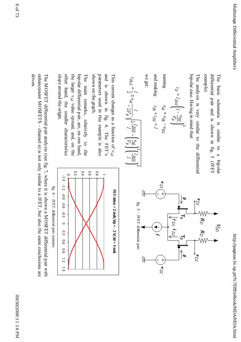
This
curren
t chan
ges as
a fu
nctio
n o
f vid
and
is
sh
ow
n in
fig.
6. T
he
F
ET
’s
param
eters u
sed in
this
examp
le is
also
show
n o
n th
e graph.
The
m
ain
remark
s,
relatively
to
th
e
bip
olar d
ifferential p
air, are, on
one h
and,
the
larger vid
valu
e sp
read, an
d, o
n th
e
oth
er han
d, th
e sm
aller ch
aracteristics
slop
e around th
e origin
.
fig. 6
– JF
ET
differen
tial pair cu
rrents
The M
OSF
ET
differen
tial pair an
alysis (see fig. 7
, where it is sh
ow
n a M
OSF
ET
differen
tial pair w
ith
enhan
cemen
t MO
SF
ET
S –
chan
nel n
) is not o
nly
similar to
a JFE
T, b
ut also
the sam
e conclu
sions are
driv
en.
Multistage
Diff
ere
ntial A
mplifi
ers
http
://pagin
as.fe.u
p.p
t/%7E
fff/e
Book/M
DA
/MD
A.h
tml
6 o
f 73
09/3
0/2
008 1
1:1
4 P
M
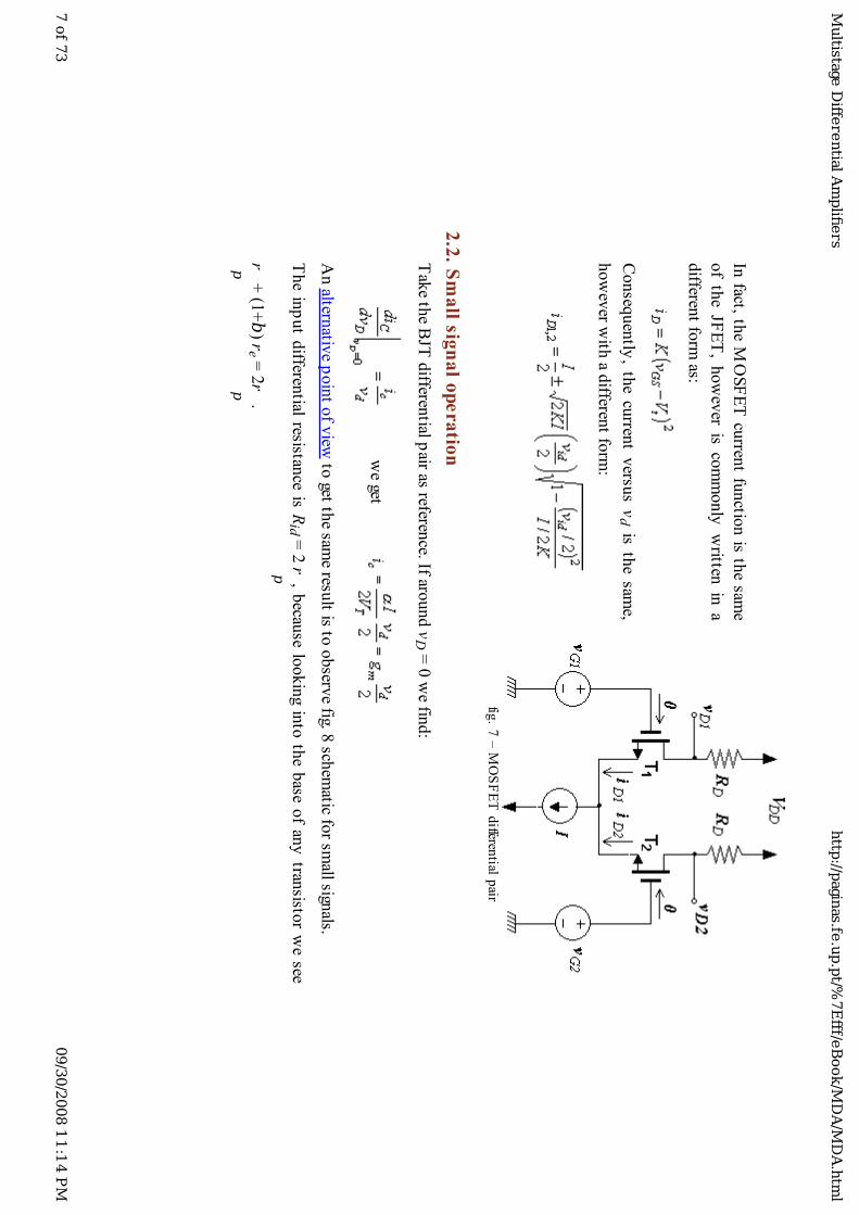
In fact, th
e M
OSF
ET
curren
t functio
n is
the sam
e
of th
e JF
ET
, how
ever is
com
mon
ly w
ritten in
a
differen
t form
as:
Con
sequen
tly, th
e cu
rrent v
ersus
vd
is th
e sam
e,
how
ever w
ith a d
ifferent fo
rm:
fig. 7
– M
OS
FE
T d
ifferential p
air
2.2
. Sm
all sig
na
l op
era
tion
Tak
e the B
JT d
ifferential p
air as reference. If aro
und v
D =
0 w
e find:
we get
An altern
ative p
oin
t of v
iew to
get the sam
e result is to
observ
e fig. 8 sch
ematic fo
r small sign
als.
The in
put d
ifferential resistan
ce is
Rid =
2 r
p
, becau
se lo
okin
g in
to th
e b
ase o
f any
transisto
r we see
rp
+ (1
+b
) re =
2rp
.
Multistage
Diff
ere
ntial A
mplifi
ers
http
://pagin
as.fe.u
p.p
t/%7E
fff/e
Book/M
DA
/MD
A.h
tml
7 o
f 73
09/3
0/2
008 1
1:1
4 P
M

Hav
ing in
min
d, fo
r examp
le, that:
for th
e three p
ossib
le outp
uts th
e follo
win
g differen
tial gains resu
lt:
fig. 8
– S
mall sig
nal o
peratio
n
This
last gain co
rresponds to
an am
plifier w
ith d
ifferential sign
als
both
at the in
put an
d o
utp
ut (fig. 9
).
There is an
oth
er way
to lo
ok in
to th
is pro
blem
:
If we co
nsid
er the am
plifier as an
ideal d
ifferential am
plifier (w
here
essentially
the
com
mon
mode
gain is
null), acco
rdin
g to
fig. 10
circuit, th
e response to
a signal v
i can b
e analy
sed w
ith th
e base o
f
T2 co
nnected
to gro
un
d: T
he co
llector o
f T2 d
oes n
ot in
fluen
ce T1 .
This
last transisto
r is in
com
mon
emitter co
nfigu
ration
with
an
emitter
resistance
RE
equal to
re2 =
1/g
m2 . T
hen
, the
gain is
app
roxim
ately:
How
ever, if th
e oth
er outp
ut is in
tended
, it is enough
to th
ink
that
both
co
llector
cu
rrents
(sign
al)
are
necessarily
eq
ual,
an
d,
conseq
uen
tly, th
e gain w
ill be sy
mm
etric of th
e indicated
abov
e.
fig. 9
– D
ifferential in
pu
t and
ou
tpu
t amp
lifier
Multistage
Diff
ere
ntial A
mplifi
ers
http
://pagin
as.fe.u
p.p
t/%7E
fff/e
Book/M
DA
/MD
A.h
tml
8 o
f 73
09/3
0/2
008 1
1:1
4 P
M
Non
etheless, it
is called
the
attentio
n u
pon
the
fact th
at th
is
configu
ration
corresp
onds
to a
varian
t o
f a
circuit
know
n as
casco
de th
at it will b
e studied
ahead
.
fig. 1
0 –
Altern
ative m
etho
d fo
r
evalu
ating
the d
ifferential
pair g
ain
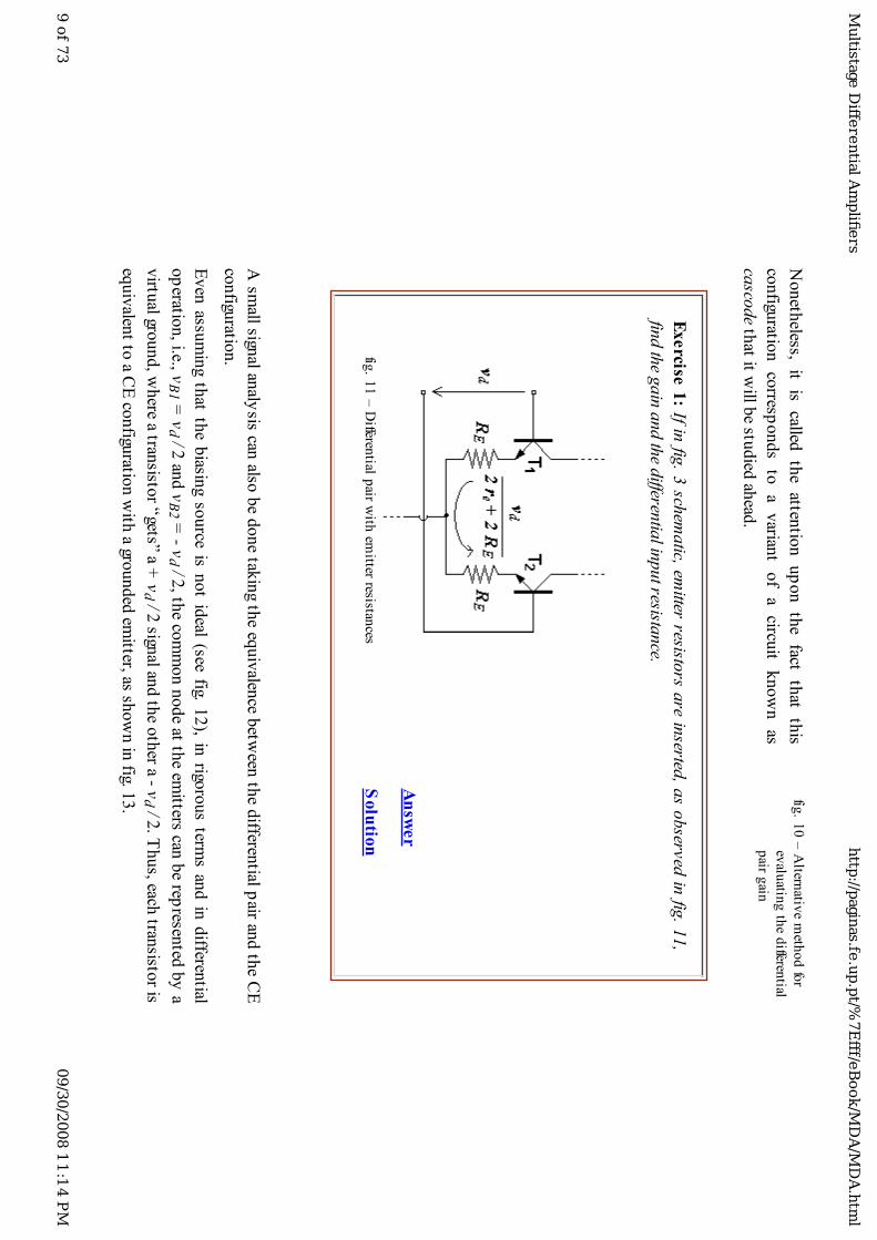
Exe
rcise 1
: If in fig
. 3 sch
ematic, em
itter resisto
rs a
re in
serted, a
s o
bserv
ed in
fig. 1
1,
find th
e gain
an
d th
e differen
tial in
put resista
nce.
fig. 1
1 –
Differen
tial pair w
ith em
itter resistances
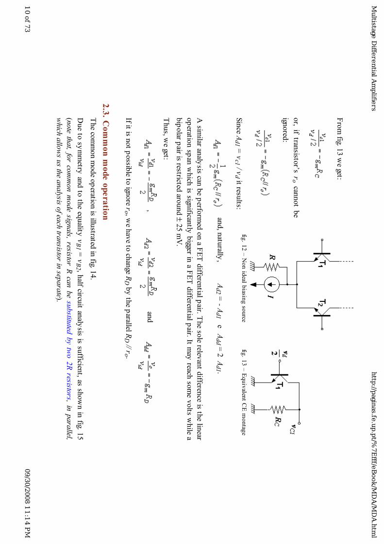
An
swe
r
Solu
tion
A sm
all signal an
alysis can
also b
e done tak
ing th
e equiv
alence b
etween
the d
ifferential p
air and
the C
E
configu
ration.
Even
assum
ing th
at the b
iasing so
urce
is n
ot id
eal (see fig. 1
2), in
rigoro
us term
s an
d in
differen
tial
op
eration, i.e., v
B1 =
vd / 2
and
vB
2 = - v
d / 2, th
e com
mon
no
de at th
e emitters can
be rep
resented
by
a
virtu
al ground, w
here a tran
sistor “
gets” a + v
d / 2 sign
al and
the o
ther a - v
d / 2. T
hus, each
transisto
r is
equiv
alent to
a CE
con
figuratio
n w
ith a gro
un
ded
emitter, as sh
ow
n in
fig. 13.
Multistage
Diff
ere
ntial A
mplifi
ers
http
://pagin
as.fe.u
p.p
t/%7E
fff/e
Book/M
DA
/MD
A.h
tml
9 o
f 73
09/3
0/2
008 1
1:1
4 P
M
Fro
m fig. 1
3 w
e get:
or, if tran
sistor’s
ro
cannot b
e
igno
red:
Sin
ce Ad
1 = v
c1 / vd it resu
lts:
fig
. 12
– N
on
ideal b
iasing
sou
rce fig. 1
3 –
Eq
uiv
alent C
E m
on
tage
and
, natu
rally, A
d2 =
- Ad
1 e Ad
d = 2
Ad
1 .
A sim
ilar analy
sis can b
e perfo
rmed
on
a FE
T d
ifferential p
air. The so
le relevan
t differen
ce is the lin
ear
op
eration
span
which
is significan
tly b
igger in a F
ET
differen
tial pair. It m
ay reach
som
e volts w
hile a
bip
olar p
air is restricted aro
und ±
25 m
V.
Thu
s, we get:
, an
d
If it is not p
ossib
le to ign
ore r
o , we h
ave to
chan
ge RD
by
the p
arallel RD
// ro .
2.3
. Co
mm
on
mo
de
op
era
tion
The co
mm
on m
ode o
peratio
n is illu
strated in
fig. 14.
Due to
sym
metry
and
to th
e equality
vB
1 = v
B2 , h
alf circuit an
alysis is su
fficient, as sh
ow
n in
fig. 15
(note
that, fo
r co
mm
on
mode sig
nals, resisto
r R
can
be su
bstitu
ted b
y tw
o 2
R resisto
rs, in p
ara
llel,
which
allo
ws u
s the a
nalysis o
f each
transisto
r in sep
ara
te).
Multistage
Diff
ere
ntial A
mplifi
ers
http
://pagin
as.fe.u
p.p
t/%7E
fff/e
Book/M
DA
/MD
A.h
tml
10 o
f 73
09/3
0/2
008 1
1:1
4 P
M

fig
. 14
– C
om
mo
n m
od
e op
eration
fig. 1
5 –
Co
mm
on
mo
de eq
uiv
alent
CE
mo
ntag
e
If RC
« r
o , we get:
and b
y an
alogy
an
d
The co
mm
on m
ode rejectio
n ratio
is, by
defin
ition,
such
that, fo
r each u
niq
ue o
utp
ut (v
c1 or v
c2 ), we get
.
Multistage
Diff
ere
ntial A
mplifi
ers
http
://pagin
as.fe.u
p.p
t/%7E
fff/e
Book/M
DA
/MD
A.h
tml
11
of 7
309/3
0/2
008 1
1:1
4 P
M

For th
e d
ifferential o
utp
ut C
MR
R =
¥, o
bvio
usly
except th
e case where th
e sym
metry
is not p
erfect.
Verify
th
at,
for
exam
ple,
if
R
C1 =
RC
an
d
RC
2 = R
C +
D R
C, w
e get:
Fig. 1
6 illu
strates a com
mon
mode in
put resistan
ce
defin
ition.
Con
siderin
g only
half-circu
it, the resistan
ce seen b
y
vC
M is 2
RiC
M .
fig. 1
6 –
Co
mm
on
mo
de in
pu
t resistance
Exe
rcise 2
: Sh
ow
that
and
expla
in w
hy in
this
con
text (where
R is
gen
erally
very
hig
h) it m
ak
es sen
se n
ot to
forg
et rm
, in g
enera
l ignored
for b
eing v
ery hig
h.
Solu
tion
2.4
. Op
era
tion
with
arb
itrary
inp
ut v
olta
ge
s
Multistage
Diff
ere
ntial A
mplifi
ers
http
://pagin
as.fe.u
p.p
t/%7E
fff/e
Book/M
DA
/MD
A.h
tml
12 o
f 73
09/3
0/2
008 1
1:1
4 P
M

It is
conven
ient
at th
is stage
to (re)in
troduce
the
inp
ut
signals
deco
mp
ositio
n issu
e, vB
1 and v
B2 , in
to tw
o n
ew v
ariables:
vD
= v
B1 –
vB
2 and v
CM
= (v
B1 +
vB
2 )/2 (fig. 1
7).
Evid
ently
, this co
nvey
s into
vB
1 = v
CM
+ v
D /2
and
vB
2 = v
CM
– v
D
/2. L
et v1 an
d v
2 be th
e signal co
mp
onen
ts of v
B1 an
d v
B2 . In
general,
the d
ifferential p
air inp
ut v
oltages, v
1 and
v2 , co
rresponds n
either to
a differen
tial nor to
a com
mon m
ode.
fig. 1
7 –
Inp
ut sig
nals
Fro
m w
hat w
as said ab
ove, w
e hav
e:
and
The o
utp
ut can
be exp
ressed as v
o = A
1 v
1 + A
2 v2 as lo
ng as th
e signals m
agnitu
de is su
ch th
at linear
op
eration can
be co
nsid
ered, w
hich
can fu
rther b
e man
ipulated
into
:
We w
ill hav
e then
Ad =
(A1 –
A2 )/2
and A
cm =
A1 +
A2 .
Rew
riting v
o expressio
n w
e get:
(where C
MR
R is exp
ressed in
non-lo
garithm
ic form
) which
then
show
s that, if th
e CM
RR
is sufficien
tly
high
, the o
utp
ut sign
al dep
ends so
lely o
n th
e inp
ut d
ifferential co
mp
on
ent.
Becau
se the d
esirable o
peratio
n is p
recisely th
is, the term
constitu
tes the erro
r of th
e differen
tial circuit m
odel.
2.5
. Oth
er n
on
-ide
al ch
ara
cteristics
Multistage
Diff
ere
ntial A
mplifi
ers
http
://pagin
as.fe.u
p.p
t/%7E
fff/e
Book/M
DA
/MD
A.h
tml
13 o
f 73
09/3
0/2
008 1
1:1
4 P
M

2.5
.1. In
pu
t offse
t vo
ltag
e
If the d
ifferential p
air is perfectly
sym
metric, w
ith th
e outp
ut v
oltage tak
en b
etween
the tw
o co
llectors
(or tw
o d
rains) an
d co
nnectin
g b
oth
inp
uts
to th
e gro
und, th
en v
O =
0. B
ecause
perfect sy
mm
etry is
imp
ossib
le, in fact v
O ¹ 0
is verified
.
Thu
s, an in
put o
ffset voltage can
be d
efined
as:
The asy
mm
etry can
result fro
m th
e lo
ad resisto
r and/o
r, transisto
r characteristics
dissim
ilitud
e. If the
load
resistors d
iffer by
DR
C (o
r DR
D), th
at is, if
or
results fo
r the B
JT p
air:
and fo
r a MO
SF
ET
pair:
The relev
ant tran
sistor ch
aracteristics resp
onsib
le fo
r inp
ut o
ffset voltage, are
the rev
erse satu
ration
curren
t IS fo
r the B
JT case, an
d th
e K
factor (o
r IDS
S ) and
the th
reshold
voltage
Vt (o
r VP) fo
r FE
Ts
case.
Thu
s, for a B
JT p
air, the o
ffset result is:
and fo
r a MO
SF
ET
pair: an
d
respectiv
ely.
Multistage
Diff
ere
ntial A
mplifi
ers
http
://pagin
as.fe.u
p.p
t/%7E
fff/e
Book/M
DA
/MD
A.h
tml
14 o
f 73
09/3
0/2
008 1
1:1
4 P
M

2.5
.2. B
ias cu
rren
t an
d in
pu
t offse
t curre
nt
Giv
en its
very
sm
all valu
es, in
put
cu
rrents
are
non-relev
ant
fo
r th
e F
ET
s d
ifferential
p
airs.
Con
sequen
tly w
e will o
nly
consid
er the case o
f a BJT
differen
tial pair.
In a sy
mm
etric pair, th
e inp
ut cu
rrents at rest are eq
ual to
:
This co
mm
on
valu
e is called th
e inp
ut b
ias curren
t (IB). D
ue to
the in
evitab
le inp
ut asy
mm
etry, th
e bias
curren
ts are in fact d
ifferent. T
his d
ifference is called
inp
ut o
ffset curren
t.
In p
articular, if tran
sistor gain
s b d
iffer by
Db
, the o
ffset is:
Up
to h
ere w
e h
ave in
dicated
a sy
mbolic
curren
t source
to b
ias th
e d
ifferential p
air. It maters
now
to
see how
can th
at curren
t source b
e realised.
Discrete circu
its are goin
g to b
e distin
guish
ed fro
m in
tegrated cu
rrent so
urce circu
its.
3. B
ias circu
its for d
iffere
ntia
l pa
irs
3.1
. Discre
te circu
its
Multistage
Diff
ere
ntial A
mplifi
ers
http
://pagin
as.fe.u
p.p
t/%7E
fff/e
Book/M
DA
/MD
A.h
tml
15 o
f 73
09/3
0/2
008 1
1:1
4 P
M

A d
iscrete co
mp
onen
t ty
pical
co
nstan
t cu
rrent
so
urce
(C
CS)
realisation is illu
strated in
fig. 18 fo
r a BJT
case.
A p
ractical examp
le w
ill allow
us an
easier router to
evalu
ate an
d
pro
ject CC
S circu
it.
We w
ill assum
e V
BB =
12 V
and
–V
EE =
-12
V, an
d th
at IC =
1 m
A
is
need
ed.
Sup
pose
th
at
the
tran
sistor
has
a
b
= 1
00
an
d
VA =
100 V
.
Tak
ing V
B =
-8 V
, for IE
@ 1
mA
, results R
3 = 3
.3 kW
.
Then
, assum
ing IB
@ 0
, we get:
fig. 1
8 –
Discrete d
ifferential p
air
bias circu
it
and R
1 = 5
R2
Cho
osin
g a curren
t at R1 an
d R
2 as bein
g app
roxim
ately 1
0%
of IC
, (so th
at IB can
be n
eglected) w
e get:
then
R2 =
40 kW
and R
1 = 2
00 kW
.
Exe
rcise 3
: Fin
d th
e source o
utp
ut resista
nce, R
, hav
ing
in m
ind
the v
alu
e of r
o and
that
the tra
nsisto
r has a
n em
itter resistor R
3 .
An
swe
r
Solu
tion
3.2
. Inte
gra
ted
circuits
The resisto
r valu
es required
by
the p
revio
us settin
g are imp
ractical for in
tegrated circu
its. On
the o
ther
han
d, go
od
match
ing tran
sistors
are easy
and
econo
mic
to fab
ricate. Furth
ermore, in
tegrated circu
its
Multistage
Diff
ere
ntial A
mplifi
ers
http
://pagin
as.fe.u
p.p
t/%7E
fff/e
Book/M
DA
/MD
A.h
tml
16 o
f 73
09/3
0/2
008 1
1:1
4 P
M

usin
g exclusiv
ely M
OS tech
nolo
gy (in
particu
lar CM
OS) really
excuse th
e use o
f resistors.
This
way
, a co
mm
on
techniq
ue u
tilised in
integrated
circuits
to realise
CC
S is
the cu
rrent m
irror. T
he b
asic cu
rrent m
irror w
ith M
OSF
ET
is
show
n in
fig. 19.
If bo
th tran
sistors
are exactly
match
ed, an
d sin
ce V
GS is
the sam
e fo
r
both
transisto
rs, their cu
rrents w
ill be eq
ual. In
fact, takin
g into
accoun
t
the
ch
annel
len
gth
modulatio
n,
th
is
equality
is
only
verified
if
VD
S2 =
VD
S1 =
VG
S . This
way
, the m
irror’s
outp
ut resistan
ce, ro
2 , is a
quality
param
eter.
If bo
th th
reshold
voltages are th
e same, b
ut d
ifferent K
factors are u
sed,
then
fig. 1
9 –
MO
SF
ET
basic
curren
t mirro
r
and
results in
:
This exp
ression
show
s that ratio
s differen
t from
the u
nit tran
sfer curren
t IO / IR
EF
ratio are attain
ed b
y
a simp
le actuatio
n o
ver th
e transisto
rs’ geom
etry.
The
basic
BJT
curren
t mirro
r con
figuratio
n is
sho
wn
in fig. 2
0,
where:
Assu
min
g T
1 º T
2 , neglectin
g th
e effects
of b
and
ro , an
d sin
ce
VB
E1 =
VB
E2 , resu
lts IO =
IRE
F .
Multistage
Diff
ere
ntial A
mplifi
ers
http
://pagin
as.fe.u
p.p
t/%7E
fff/e
Book/M
DA
/MD
A.h
tml
17 o
f 73
09/3
0/2
008 1
1:1
4 P
M
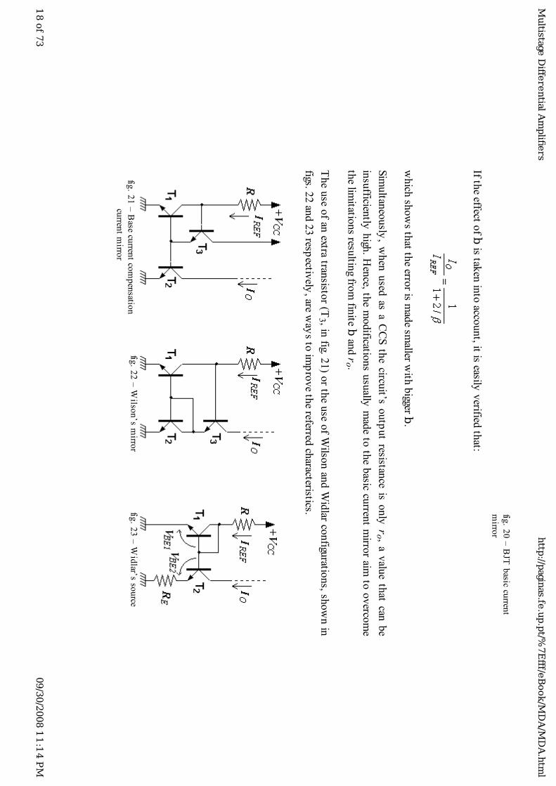
fig. 2
0 –
BJT
basic cu
rrent
mirro
r
If the effect o
f b is tak
en in
to acco
unt, it is easily
verified
that:
which
show
s that th
e error is m
ade sm
aller with
bigger b
.
Sim
ultan
eously
, when
used
as a
CC
S th
e circu
it’s o
utp
ut resistan
ce is
only
ro , a
valu
e th
at can b
e
insu
fficiently
high
. Hen
ce, the m
od
ifications u
sually
mad
e to th
e basic cu
rrent m
irror aim
to o
verco
me
the lim
itations resu
lting fro
m fin
ite b an
d r
o .
The u
se of an
extra transisto
r (T3 , in
fig. 21
) or th
e use o
f Wilso
n an
d W
idlar co
nfigu
rations, sh
ow
n in
figs. 22 an
d 2
3 resp
ectively
, are way
s to im
pro
ve th
e referred ch
aracteristics.
fig. 2
1 –
Base cu
rrent co
mp
ensatio
n
curren
t mirro
r
fig. 2
2 –
Wilso
n’s m
irror
fig. 2
3 –
Wid
lar’s sou
rce
Multistage
Diff
ere
ntial A
mplifi
ers
http
://pagin
as.fe.u
p.p
t/%7E
fff/e
Book/M
DA
/MD
A.h
tml
18 o
f 73
09/3
0/2
008 1
1:1
4 P
M

Exe
rcise 4
: Fin
d Io a
nd/o
r Ro fo
r the fo
llow
ing co
nfig
ura
tions:
a) fig
. 21
b) fig
. 22
c) fig. 2
3.
An
swe
r
Solu
tion
The cu
rrent m
irrors
outp
ut resistan
ce m
ade w
ith M
OS
can also
be in
creased u
sing W
ilson
or casco
de
configu
rations.
4. Im
pro
vin
g th
e b
an
dw
idth
Recall th
at the am
plifier b
andw
idth
refers to th
e frequen
cy ran
ge with
in w
hich
the gain
remain
s almost
constan
t. We call (lo
wer an
d u
pp
er) cut-o
ff frequen
cies to
those ran
ge lim
its. The criterio
n u
tilised to
defin
e these freq
uen
cies corresp
ond
s to th
e measu
re of th
e po
int w
here th
e maxim
um
gain d
ecreases by
3 d
B, i.e., ab
out 3
0%
gain v
alue
decrease
(3 d
B m
eans
halv
ing
the
electric p
ow
er, which
from
the
voltage p
oin
t of v
iew co
rresponds to
1 /
@ 0
.70
7).
At th
e low
er limit, i.e., at lo
w freq
uen
cies, capacitiv
e coup
ling u
tilisation
is responsib
le for th
e gain. S
o,
when
direct co
up
ling is u
sed, su
ch as w
ith in
tegrated O
pA
mp
s, usu
ally th
ere is no
gain d
ecrease at low
frequ
encies, acco
rdin
gly th
e low
er cut-o
ff frequen
cy is z
ero.
How
ever, at
high
frequen
cies, du
e to
transisto
r’s in
trinsic
capacitiv
e effect
the
gain d
ecrease is
unav
oid
able. O
therw
ise infin
ite frequen
cies would
imp
ly electro
ns (o
r oth
er carriers, such
as holes in
p
typ
e sem
iconducto
rs) infin
ite acceleratio
ns, an
d th
erefore
infin
ite fo
rces w
ould
be p
resent, w
hich
are
Multistage
Diff
ere
ntial A
mplifi
ers
http
://pagin
as.fe.u
p.p
t/%7E
fff/e
Book/M
DA
/MD
A.h
tml
19 o
f 73
09/3
0/2
008 1
1:1
4 P
M

obvio
usly
imp
ossib
le in
Natu
re. The
up
per cu
t-off freq
uen
cy d
epen
ds
not o
nly
on
the
transisto
rs
characteristics an
d q
uiescen
t poin
t but as w
ell on th
e chosen
circuit co
nfigu
ration.
Then
, in a d
irect coup
ling am
plifier, th
e ban
dw
idth
coin
cides w
ith th
e up
per cu
t-off freq
uen
cy.
4.1
. CE
con
figu
ratio
n b
an
dw
idth
The C
E b
ehav
iour at h
igh freq
uen
cies is of sp
ecial interest to
study
the d
ifferential p
air, becau
se, as we
hav
e seen
befo
re, the d
ifferential p
air is so
meh
ow
equiv
alent to
a C
E m
ontage. F
rom
the th
ree b
asic
configu
rations, it is
precisely
the C
E th
at has
the sm
allest ban
dw
idth
, i.e., it has
the sm
allest up
per
cut-o
ff frequen
cy.
The
reason
for th
is p
oorer b
ehav
iour at h
igh freq
uen
cies can
easily b
e fo
un
d th
rough
a sim
plified
analy
sis o
f the h
igh freq
uen
cy eq
uiv
alent circu
it of fig. 2
4, w
here
ro w
as ign
ored
and, fo
r the sak
e o
f
simp
licity, w
e hav
e also o
mitted
the b
ase biasin
g mesh
.
fig. 2
4 - C
E h
igh
frequ
ency
equ
ivalen
t circuit
Multistage
Diff
ere
ntial A
mplifi
ers
http
://pagin
as.fe.u
p.p
t/%7E
fff/e
Book/M
DA
/MD
A.h
tml
20 o
f 73
09/3
0/2
008 1
1:1
4 P
M

Part o
f the an
swer, in
dicated
in E
xercise 5
, can b
e o
btain
ed in
a sim
plified
man
ner w
ith th
e h
elp o
f
Miller’s th
eorem
to th
e Cm
capacito
r, consid
ering th
e mid
ban
d gain
valu
e (AM
F ).
Multistage
Diff
ere
ntial A
mplifi
ers
http
://pagin
as.fe.u
p.p
t/%7E
fff/e
Book/M
DA
/MD
A.h
tml
21
of 7
309/3
0/2
008 1
1:1
4 P
M

Indeed
, observ
ing fig. 2
5, o
ne can
notice th
at the gain
, in
spite
decreasin
g w
ith freq
uen
cy, little
differs
from
the
mid
ban
d v
alue in
the v
icinity
of th
e first pole. T
herefo
re,
this v
alue can
be u
sed to
give an
app
roxim
ate valu
e of th
e
first pole freq
uen
cy. O
n th
e oth
er han
d, it sh
ould
be clear
that it is
an ab
surd
to u
se th
e m
idban
d v
alue fo
r high
er
frequ
encies.
fig. 2
5 –
Mid
ban
d g
ain an
d first p
ole
Thu
s, the resu
lting sch
ematic (fig. 2
6) is v
alid o
nly
to d
etermin
e the b
andw
idth
(wH
@ w
p1 ), an
d n
ot
the freq
uen
cy resp
onse in
total. B
esides, it is n
oto
rious th
at the z
ero d
isapp
ears in th
is analy
sis.
Fro
m fig. 2
6 w
e get
, an
d
The K
valu
e is easily o
btain
ed:
Sin
ce it is a large negativ
e valu
e,
results:
and
fig. 2
6 –
HF
equ
ivalen
t circuit o
f the C
E m
on
tage sim
plified
by
app
lication
of M
iller’s theo
rem
Then
, the tim
e constan
ts associated
with
both
indep
enden
t capacito
rs are:
and
with
Multistage
Diff
ere
ntial A
mplifi
ers
http
://pagin
as.fe.u
p.p
t/%7E
fff/e
Book/M
DA
/MD
A.h
tml
22 o
f 73
09/3
0/2
008 1
1:1
4 P
M

and co
rrespondin
g poles
and
Sin
ce in gen
eral, w1 <
< w
2 , the b
and lim
it may
be co
nsid
ered co
incid
ent w
ith w
1 :
On
the o
ther h
and, th
e m
iddle-freq
uen
cy gain
app
roxim
ation
used
does n
ot allo
w th
e id
entificatio
n o
f
w2 as th
e second p
ole o
f the o
riginal circu
it.
A m
ore a
ccura
te estimatio
n fo
r the first p
ole a
nd
also
for th
e second
one ca
n b
e obta
ined
, alth
ough
more
onero
usly, u
sing th
e time co
nsta
nts m
ethod.
Note, as
reference, th
at C
p
and
Cm
hav
e ty
pical v
alues
in th
e o
rder
of ten
s an
d u
nities
of p
F,
respectiv
ely. B
esides
the fact th
at Cm
is sm
all, its actu
al contrib
utio
n is
large b
ecause
the cap
acitor
valu
e is multip
lied b
y th
e configu
ration gain
. This is k
now
n as th
e Miller m
ultip
licative effect.
Let u
s m
ake a
reference
to th
e z
ero. In
fig. 24
schem
atic, the o
utp
ut v
oltage
is an
nulled
when
the C
m
capacito
r curren
t is equal to
the cu
rrent so
urce cu
rrent, i.e., w
hen
the cu
rrent in
RC
is zero
. Then
,
This is th
e frequen
cy o
f the z
ero, w
hich
coin
cides w
ith th
e calculated
valu
e in E
xercise 5. H
ow
ever, o
ne
shou
ld n
ote th
at, given
the cap
acitor v
alues an
d assu
min
g gm
in th
e ord
er of 1
00
mA
/V, th
e zero
will b
e
situated
at a freq
uen
cy m
uch
high
er than
the p
oles. A
t the p
resent p
oin
t this
does
not seem
of great
Multistage
Diff
ere
ntial A
mplifi
ers
http
://pagin
as.fe.u
p.p
t/%7E
fff/e
Book/M
DA
/MD
A.h
tml
23 o
f 73
09/3
0/2
008 1
1:1
4 P
M

imp
ortan
ce how
ever, atten
tion
sho
uld
be called
up
on
the fact th
at the z
ero is lo
cated o
n th
e right h
and
side o
f the S
plan
e (it is real and
po
sitive). U
nexp
ectedly
, this z
ero in
troduces a p
hase d
elay an
d n
ot a
delay
advan
ce. In th
is persp
ective b
ehav
es as a pole o
n th
e left han
d sid
e of th
e S p
lane.
In th
e com
mon
base an
d co
mm
on
collecto
r configu
rations th
e Miller m
ultip
licative effect d
oes n
ot exist.
The last h
as th
e C
p
capacito
r betw
een tw
o n
odes
with
slightly
less th
an o
ne p
ositiv
e gain
, and
the
form
er has
both
capacito
rs to
grou
nd: th
e M
iller effect is th
en o
ut o
f the q
uestio
n. In
this
way
, both
configu
rations p
resent m
uch
high
er up
per cu
t-off freq
uen
cies. It is kno
wn
that in
a given
configu
ration
the gain
ban
dw
idth
pro
duct is ap
pro
ximately
constan
t - if the gain
increases th
e ban
dw
idth
dim
inish
es.
Fro
m all co
nsid
ered co
nfigu
rations, o
nly
the C
E co
nfigu
ration
show
s both
bigger th
an o
ne cu
rrent an
d
voltage
gains. T
he C
C co
nfigu
ration
has
un
it voltage
gain an
d B
C h
as a
unit cu
rrent gain
. Thus, in
a
certain w
ay, it is “
natu
ral” that th
e existence o
f two large gain
s mak
e the b
andw
idth
dim
inish
.
Fro
m th
is an
alysis
results
a relativ
ely p
oor h
igh freq
uen
cy b
ehav
iour fo
r the C
E co
nfigu
ration
(thus,
also fo
r the d
ifferential p
air), which
need
s to b
e imp
roved
.
One co
nfigu
ration w
ith a C
E eq
uiv
alent v
oltage gain
but larger b
andw
idth
is the casco
de p
air.
4.2
. CE
-CB
Ca
scod
e p
air
Fig. 2
7 (a) rep
resents a b
iasing sch
eme fo
r the casco
de p
air and
in (b
) the eq
uiv
alent circu
it for sign
als,
where R
B =
R1 // R
2 .
Multistage
Diff
ere
ntial A
mplifi
ers
http
://pagin
as.fe.u
p.p
t/%7E
fff/e
Book/M
DA
/MD
A.h
tml
24 o
f 73
09/3
0/2
008 1
1:1
4 P
M

fig. 2
7 - C
E-C
B casco
de p
air; (a) bias circu
it; (b) sm
all sign
al equ
ivalen
t circuit
Low
frequen
cy an
alysis o
f fig. 27 sch
ematic giv
es:
which
insigh
ts that an
equiv
alent C
E v
o / vi gain
can b
e built w
ith an
equal tran
sistor b
iased at th
e same
DC
op
erating p
oin
t.
How
ever a d
ifference is in
favour o
f the casco
de co
nfigu
ration.
In fact, a
large R
C is
adop
ted w
hen
a large
gain is
need
ed. If R
C is
sufficien
tly large, th
e r
o >>
RC
app
roxim
ation m
ay n
o lo
nger b
e acceptab
le. Then
for a C
E w
e should
consid
er:
Multistage
Diff
ere
ntial A
mplifi
ers
http
://pagin
as.fe.u
p.p
t/%7E
fff/e
Book/M
DA
/MD
A.h
tml
25 o
f 73
09/3
0/2
008 1
1:1
4 P
M

If RC
>>
ro , th
e maxim
um
gain is giv
en b
y –
gm
ro .
To
examin
e w
hat
takes
place
with
the
cascode
configu
ration
, let u
s d
etermin
e
Gm
and
Ro
relatively
to th
e eq
uiv
alent
mod
el of fig. 2
7 (a) an
d rep
resented
in fig.
28.
Calcu
lating G
m, giv
es:fig
. 28
- Casco
de p
air equ
ivalen
t circuit
To calcu
late Ro , fig. 2
9 is u
sed.
Multistage
Diff
ere
ntial A
mplifi
ers
http
://pagin
as.fe.u
p.p
t/%7E
fff/e
Book/M
DA
/MD
A.h
tml
26 o
f 73
09/3
0/2
008 1
1:1
4 P
M

fig. 2
9 - E
valu
ation
of o
utp
ut resistan
ce Ro ; (a) D
eactivatin
g th
e ind
epen
den
t sou
rces; (b) C
ircuit sim
plificatio
n
A d
eactivatio
n co
nditio
n w
as imp
osed
to th
e indep
enden
t sou
rces in fig. 2
9 (a), w
hich
annuls th
e fonte
gm
1 vp
1
curren
t so
urce. G
iven
that
ro
1 >>
rp
2
, then
the
parallel is
app
roxim
ately r
p2
. Fin
ally,
app
lyin
g th
e T
hév
enin
’s th
eorem
results
in fig. 2
9 (b
) schem
atic, where
the
outp
ut resistan
ce can
imm
ediately
be fo
und to
be:
where it w
as consid
ered r
o = r
o1 =
ro
2 (equ
al transisto
rs with
the sam
e op
erating p
oin
t). Then
for th
e
voltage gain
we get:
Multistage
Diff
ere
ntial A
mplifi
ers
http
://pagin
as.fe.u
p.p
t/%7E
fff/e
Book/M
DA
/MD
A.h
tml
27 o
f 73
09/3
0/2
008 1
1:1
4 P
M

Hen
ce the m
aximum
gain v
alue w
ill be –
gm
b r
o , wh
ich is co
nsid
erably
larger than
the co
mm
on
emitter
gain.
As m
entio
ned
above, th
e cascode b
andw
idth
is larger than
the eq
uiv
alent co
mm
on
emitter. L
et us ch
eck
why
with
a simp
lified q
ualitativ
e analy
sis.
The casco
de seco
nd
stage is a com
mon
base am
plifier, w
hich
frequen
cy resp
onse is v
ery go
od. S
o, it is
the first stage, a
com
mon
emitter, th
at will p
rimarily
conditio
n th
e h
igh freq
uen
cy resp
onse. T
he C
E
low
er cut o
ff frequen
cy resu
lts from
the M
iller multip
licative effect o
ver th
e Cm
1 capacito
r. How
ever,
becau
se the first stage lo
ad is th
e second
stage low
inp
ut resistan
ce (re ), th
e Miller m
ultip
licative facto
r
will b
e solely
:
This w
ay, th
e up
per cu
t-off freq
uen
cy o
f the circu
it will b
e consid
erably
larger than
the u
pp
er cut-o
ff
frequ
ency
of a C
E.
4.3
. CE
-CB
com
ple
me
nta
ry ca
scod
e
Fig. 3
0 (a) rep
resents
the b
iasing sch
eme o
f a co
mp
lemen
tary casco
de p
air and
in (b
) the eq
uiv
alent
circuit fo
r signal an
alysis.
Multistage
Diff
ere
ntial A
mplifi
ers
http
://pagin
as.fe.u
p.p
t/%7E
fff/e
Book/M
DA
/MD
A.h
tml
28 o
f 73
09/3
0/2
008 1
1:1
4 P
M
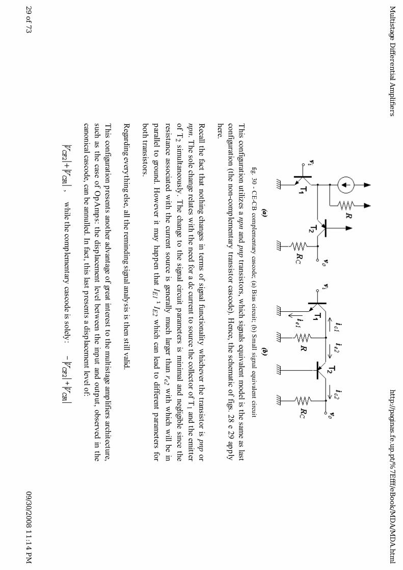
fig. 3
0 - C
E-C
B co
mp
lemen
tary casco
de; (a) B
ias circuit; (b
) Sm
all sign
al equ
ivalen
t circuit
This co
nfigu
ration
utiliz
es a npn
and
pnp
transisto
rs, which
signals eq
uiv
alent m
odel is th
e same as last
configu
ration
(the n
on
-com
plem
entary
transisto
r cascode). H
ence, th
e schem
atic of figs. 2
8 e 2
9 ap
ply
here.
Recall th
e fact th
at no
thin
g ch
anges
in term
s o
f signal fu
nctio
nality
which
ever th
e tran
sistor is
pnp
or
npn. T
he so
le chan
ge relates with
the n
eed fo
r a dc cu
rrent to
source th
e collecto
r of T
1 and
the em
itter
of T
2 sim
ultan
eously
. The ch
ange
to th
e sign
al circuit p
arameters
is m
inim
al and
negligib
le sin
ce th
e
resistance
associated
with
the cu
rrent so
urce
is gen
erally m
uch
larger than
re2
with
which
will b
e in
parallel to
ground. H
ow
ever it m
ay h
app
en th
at IE1 ¹ IE
2 w
hich
can lead
to d
ifferent p
arameters
for
both
transisto
rs.
Regard
ing ev
eryth
ing else, all th
e remin
din
g signal an
alysis is th
en still v
alid.
This co
nfigu
ration
presen
ts anoth
er advan
tage of great in
terest to th
e multistage am
plifiers arch
itecture,
such
as th
e case
of O
pA
mp
s: the d
isplacem
ent lev
el betw
een th
e in
put an
d o
utp
ut, o
bserv
ed in
the
cano
nical casco
de, can
be an
nulled
. In fact, th
is last presen
ts a disp
lacemen
t level o
f:
, while th
e com
plem
entary
cascode is so
lely:
Multistage
Diff
ere
ntial A
mplifi
ers
http
://pagin
as.fe.u
p.p
t/%7E
fff/e
Book/M
DA
/MD
A.h
tml
29 o
f 73
09/3
0/2
008 1
1:1
4 P
M
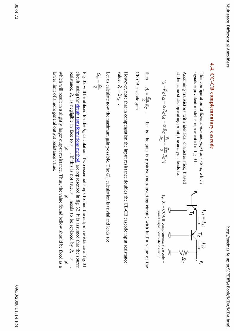
4.4
. CC
-CB
com
ple
me
nta
ry ca
scod
e
This co
nfigu
ration
utiliz
es a npn
and
pnp
transisto
rs, which
signals eq
uiv
alent m
od
el is represen
ted in
fig. 31.
Assu
min
g tran
sistors
with
iden
tical characteristics, b
iased
at the sam
e static op
erating p
oin
t, the an
alysis lead
s to:
fig. 3
1 –
CC
-CB
com
plem
entary
cascod
e –
small sig
nal eq
uiv
alent circu
it
then
, th
at is, the
gain is
positiv
e (n
on-in
vertin
g circu
it) with
half a
valu
e o
f the
CE
-CB
cascode gain
.
How
ever, n
ote th
at in co
mp
ensatio
n th
e inp
ut resistan
ce doub
les the C
E-C
B casco
de in
put resistan
ce
valu
e: .
Let u
s calculate n
ow
the m
aximum
gain p
ossib
le. The G
m calcu
lation is triv
ial and lead
s to:
.
Fig. 3
2 w
ill be u
tilised fo
r the R
o calculatio
n. T
wo
essential step
s to fin
d th
e outp
ut resistan
ce of fig. 3
1
circuit, u
sing th
e circuit tran
sform
ations m
ethod, are rep
resented
in fig. 3
2. It is assu
med
that th
e source
resistance, R
s , is n
egligible
in face
to r
p1
. If this
is n
ot tru
e, rp
1
need
s to
be rep
laced b
y R
s + r
p1
,
which
will resu
lt in a sligh
tly larger o
utp
ut resistan
ce. Thus, th
e valu
e found
bello
w sh
ould
be faced
as a
low
er limit o
f a more gen
eral outp
ut resistan
ce valu
e.
Multistage
Diff
ere
ntial A
mplifi
ers
http
://pagin
as.fe.u
p.p
t/%7E
fff/e
Book/M
DA
/MD
A.h
tml
30 o
f 73
09/3
0/2
008 1
1:1
4 P
M
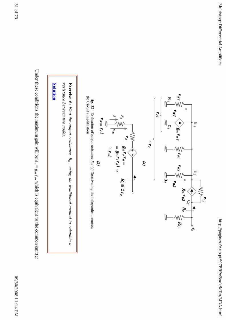
fig. 3
2 - E
valu
ation
of o
utp
ut resistan
ce Ro ; (a) D
eactivatin
g th
e ind
epen
den
t sou
rces;
(b) C
ircuit sim
plificatio
n
Exe
rcise 6
: Fin
d th
e o
utp
ut resista
nce, R
o , u
sing
the tra
ditio
nal m
ethod
to ca
lcula
te a
resistance b
etween
two n
odes.
Solu
tion
Und
er these co
nditio
ns th
e maxim
um
gain w
ill be A
v = g
m r
o , which
is equiv
alent to
the co
mm
on
emitter
Multistage
Diff
ere
ntial A
mplifi
ers
http
://pagin
as.fe.u
p.p
t/%7E
fff/e
Book/M
DA
/MD
A.h
tml
31
of 7
309/3
0/2
008 1
1:1
4 P
M

gain.
Concern
ing b
andw
idth
, one m
ight ev
aluate
it in a
simp
le way
. Note th
at capacito
r Cm
1 is con
nected
to th
e ground, as w
ell as Cp
2 and C
m2 (see fig. 3
3).
On
the
oth
er han
d, cap
acitor C
p1
connects
two
nodes w
ith a gain
that can
easily b
e found to
be ½
.fig
. 33
– C
apacities in
the C
C-C
B m
on
tage
This gain
is indep
end
ent o
f frequen
cy an
d m
eans th
at the M
iller’s th
eorem
can b
e ap
plied
rigoro
usly
,
i.e., with
out th
e usu
al restriction
that resu
lts from
the ap
pro
ximatio
n to
the m
idban
d gain
. In th
is way
,
the fo
llow
ing fig. 3
4 sch
ematic resu
lts.
fig. 3
4 –
CC
-CB
mo
ntag
e equ
ivalen
t circuit ap
ply
ing
Miller’s th
eorem
to C
p
1
Sin
ce - C
p1
and
Cp
2
annul each
oth
er, the circu
it on
ly p
resents
two
indep
end
ent cap
acitances, w
hich
time co
nstan
ts are:
and
Which
corresp
ondin
g p
oles
will b
e d
om
inan
t or, at least, w
hich
will h
ave
the
low
est frequen
cy, is
Multistage
Diff
ere
ntial A
mplifi
ers
http
://pagin
as.fe.u
p.p
t/%7E
fff/e
Book/M
DA
/MD
A.h
tml
32 o
f 73
09/3
0/2
008 1
1:1
4 P
M

dep
enden
t on
circuit p
arameters. H
ow
ever, it is n
oto
rious th
at any
of th
em o
ccur at a h
igher freq
uen
cy
than
the co
mm
on em
itter and ev
en h
igher th
an th
e CE
-CB
con
figuratio
n.
One
migh
t reach th
is co
nclu
sion
qualitativ
ely. In
reality, th
e C
C-C
B co
nfigu
ration
is m
ade
of tw
o
stages, both
with
very
good
high
frequen
cy resp
onses. In
particu
lar, the first stage, a co
mm
on
collecto
r,
has a u
pp
er cut-o
ff frequen
cy larger th
an th
e low
-gain co
mm
on
emitter, su
ch as th
e case of th
e CE
-CB
cascode. E
qually
the seco
nd stage is a co
mm
on b
ase with
a very
high
cut-o
ff frequen
cy.
4.5
. Ca
scod
e d
iffere
ntia
l pa
ir
The
good
frequen
cy resp
onse
pro
perties
found
in a
com
plem
entary
cascode
are u
tilized
in th
e
differen
tial pair casco
de, w
hich
schem
atic can b
e seen in
fig. 35. T
his co
nfigu
ration
is used
as an in
put
stage, e.g, in th
e 741 O
pA
mp
.
fig. 3
5 - D
ifferential casco
de p
air; (a) Sim
plified
bias circu
it; (b) S
mall sig
nal eq
uiv
alent circu
it
Multistage
Diff
ere
ntial A
mplifi
ers
http
://pagin
as.fe.u
p.p
t/%7E
fff/e
Book/M
DA
/MD
A.h
tml
33 o
f 73
09/3
0/2
008 1
1:1
4 P
M
To fin
d th
e voltage gain
note th
at:
then
and
from
which
we co
nclu
de th
at the gain
is half o
f that o
ne fo
und
in a sim
ple d
ifferential p
air. On
the
oth
er han
d th
e inp
ut resistan
ce is do
uble:
.
The u
se of a casco
de d
ifferential p
air imp
roves th
e general ch
aracteristics of th
e pair, alth
ough
it seems
to red
uce th
e gain. N
ote, h
ow
ever, th
at the m
aximum
gain lim
it is the sam
e of a sim
ple d
ifferential p
air.
This d
iscussio
n ab
out th
e gain raises a q
uestio
n ab
ou
t the gain
allow
ed b
y th
e differen
tial pair an
d if it
is sufficien
t to attain
the ty
pical v
alues p
resented
by
a general p
urp
ose O
pA
mp
.
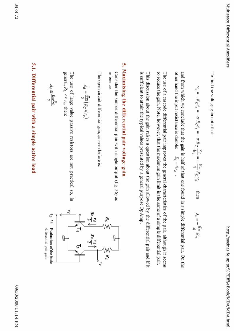
5. M
ax
imisin
g th
e d
iffere
ntia
l pa
ir vo
ltag
e g
ain
Con
sider th
e sim
ple
differen
tial pair w
ith sin
gle o
utp
ut (fig. 3
6) as
reference.
The o
pen
circuit d
ifferential gain
, as seen b
efore is:
The
use
of large
valu
e p
assive
resistors
are n
ot p
ractical so, in
general, R
C <
< r
o , then
:
fig. 3
6 –
Ev
aluatio
n o
f the b
asic
differen
tial pair g
ain
5.1
. Diffe
ren
tial p
air w
ith a
simp
le a
ctive
loa
d
Multistage
Diff
ere
ntial A
mplifi
ers
http
://pagin
as.fe.u
p.p
t/%7E
fff/e
Book/M
DA
/MD
A.h
tml
34 o
f 73
09/3
0/2
008 1
1:1
4 P
M

The gain
can b
e co
nsid
erably
increased
if an activ
e lo
ad is
used
instead
of a p
assive o
ne, i.e., a cu
rrent so
urce setu
p w
ith o
utp
ut
resistance R
o , which
, as seen b
efore, can
be sev
eral times larger
than
ro (fig. 3
7).
The an
alysis lead
s to a gain
valu
e of:
Thu
s, for exam
ple, if R
o = 4
ro , w
e get:
fig. 3
7 –
Sm
all sign
al equ
ivalen
t circuit
for th
e differen
tial pair w
ith
sing
le active lo
ad
5.2
. Diffe
ren
tial p
air w
ith cu
rren
t mirro
r activ
e lo
ad
A larger v
alue fo
r the gain
can b
e obtain
ed if a cu
rrent m
irror is
used
as load
, like fig. 3
8 sh
ow
s.
The m
irror effect lead
s to:
and
if ro
2 = r
o4 =
ro co
mes:
which
is larger than
what can
be fo
und w
ith a sim
ple activ
e load
.
This
valu
e can
be fu
rther im
pro
ved
usin
g a
mirro
r with
high
er
outp
ut resistan
ce (fig. 39).
fig. 3
8 –
Sm
all sign
al equ
ivalen
t circuit
Multistage
Diff
ere
ntial A
mplifi
ers
http
://pagin
as.fe.u
p.p
t/%7E
fff/e
Book/M
DA
/MD
A.h
tml
35 o
f 73
09/3
0/2
008 1
1:1
4 P
M

for
the d
ifferential p
air with
curren
t
mirro
r active lo
ad
fig. 3
9 - D
ifferential p
air with
curren
t mirro
r active lo
ad; (a) sy
mm
etric Wid
lar's mirro
r;
(b) b
ase curren
t com
pen
sation
curren
t mirro
r
Eith
er usin
g the W
idlar’s sy
mm
etric mirro
r (fig. 39
(a)), or th
e base cu
rrent co
mp
ensatio
n m
irror (fig. 3
9
(b)), w
e get:
bein
g ro
2 = r
o4 =
ro , b
ecause R
o4 >
ro , th
en:
For exam
ple, if R
o4 =
4 r
o , then
:
Hen
ce, we m
ay co
nclu
de th
at the o
pen
circuit m
aximum
gain (it lo
wers w
ith th
e load
), is in th
e ord
er of
gm
ro / 2
(it migh
t only
be sligh
tly larger). S
ince
then
, for exam
ple, if w
e consid
er VA
= 1
00 V
, com
es:
Multistage
Diff
ere
ntial A
mplifi
ers
http
://pagin
as.fe.u
p.p
t/%7E
fff/e
Book/M
DA
/MD
A.h
tml
36 o
f 73
09/3
0/2
008 1
1:1
4 P
M

Alth
ough
it migh
t be raised
by
a small am
ou
nt, th
is valu
e is well b
ellow
the u
sual ten
s or h
undred
s of
thou
sands gain
valu
es characteristics o
f Op
Am
ps.
Even
indep
enden
tly o
f oth
er consid
erations, su
ch as th
e ones relativ
e to th
e outp
ut resistan
ce, it is clear
that a d
ifferential p
air is insu
fficient to
realize an
amp
lifier with
Op
Am
p lik
e characteristics. A
second
stage (at least) is need
ed to
attain th
e desired
gain lev
el.
The seco
nd
stage n
eeds to
hav
e a
reasonab
le large
valu
e o
f gain (at least so
me ten
s) and
a large
inp
ut
resistance to
avoid
gain d
egradatio
n o
f the first stage am
plifier. A
low
outp
ut resistan
ce, as it is required
by
an O
pA
mp
structu
re, is also
desirab
le. Note
how
ever th
at this
stage d
oes
not n
eed to
hav
e a
differen
tial inp
ut.
5.3
. On
e C
MO
S d
iffere
ntia
l pa
ir with
activ
e lo
ad
Fig. 4
0 sh
ow
s an
examp
le o
f a C
MO
S d
ifferential p
air with
active lo
ad.
The o
utp
ut d
c v
oltage
is, norm
ally, estab
lished
by
the n
ext
stage as can b
e seen in
the O
pA
mp
intern
al circuits.
The
circuit
is an
alogo
us
to th
e b
ipolar
versio
n. T
hus, th
e
curren
t signal is: w
here
The o
utp
ut v
oltage is:
With
fig
. 40
- CM
OS
differen
tial pair w
ith
active lo
ad
Multistage
Diff
ere
ntial A
mplifi
ers
http
://pagin
as.fe.u
p.p
t/%7E
fff/e
Book/M
DA
/MD
A.h
tml
37 o
f 73
09/3
0/2
008 1
1:1
4 P
M

the v
oltage gain
com
es:
To
get high
gains, o
ne d
ifferential casco
de an
d o
ne casco
de cu
rrent m
irror can
be u
sed. H
ow
ever, th
is
low
ers the o
utp
ut sign
al excursio
n p
ossib
le.
The u
se o
f FE
Ts is
specially
interestin
g b
ecause
of th
e v
ery h
igh in
put resistan
ces th
at is allo
wed
to
get. The o
ffset voltage is in
the sam
e ord
er (som
e miliv
olts) o
f the b
ipolar d
ifferential p
airs but, th
e bias
curren
ts at the in
put are m
uch
smaller th
an w
hat is p
ossib
le to m
ake w
ith b
ipolar tran
sistors.
The m
ajor F
ET
s in
conven
ience
is th
e lo
w tran
scon
ductan
ce an
d, co
nseq
uen
tly, th
e lo
wer larger gain
possib
le.
Now
aday
s, integrated
Op
Am
ps are fab
ricated u
sing C
MO
S tech
nolo
gy. T
he gen
eral characteristics are
good
and v
ery lo
w p
ow
er voltages (1
V!) can
be u
sed w
ith v
ery lo
w p
ow
er consu
mp
tion.
6. H
igh
vo
ltag
e g
ain
an
d in
pu
t resista
nce
stag
es
6.1
. Th
e D
arlin
gto
n p
air –
CC
-CC
con
figu
ratio
n
Multistage
Diff
ere
ntial A
mplifi
ers
http
://pagin
as.fe.u
p.p
t/%7E
fff/e
Book/M
DA
/MD
A.h
tml
38 o
f 73
09/3
0/2
008 1
1:1
4 P
M

Let’s co
nsid
er the circu
it of fig. 4
1, w
here th
e biasin
g com
po
nen
ts
are om
itted.
If we su
pp
ose th
at T1 º
T2 an
d th
at they
are equally
biased
, let’s
com
pute th
e voltage gain
and in
put resistan
ce:
fig. 4
1 - S
imp
lified sch
ematic o
f
the D
arling
ton
pair
that lead
s to
If b »
2, w
e hav
e:
and if g
m R
E >
> 1
, we m
ay w
rite the ap
pro
ximate v
alue o
f Av :
which
is the sam
e expressio
n w
e get for th
e single tran
sistor em
itter follo
wer.
But th
e inp
ut resistan
ce, if b >
> 1
and
RE >
> 1
1/g
m is:
much
larger than
the v
alue b
RE, th
at is the ap
pro
ximate v
alue w
e get for a sin
gle transisto
r.
In th
e same w
ay, th
e short-circu
it curren
t gain is (b
+1) 2 m
uch
larger than
(b +
1) th
at the sin
gle stage
Multistage
Diff
ere
ntial A
mplifi
ers
http
://pagin
as.fe.u
p.p
t/%7E
fff/e
Book/M
DA
/MD
A.h
tml
39 o
f 73
09/3
0/2
008 1
1:1
4 P
M
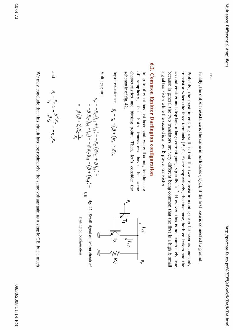
has.
Fin
ally, th
e outp
ut resistan
ce is the sam
e in b
oth
cases (1/g
m), if th
e first base is co
nnected
to gro
un
d.
Pro
bab
ly, th
e m
ost in
teresting
result is
that th
e tw
o tran
sistor m
ontage
can b
e seen
as o
ne
only
transisto
r where
the th
ree term
inals
(B, C
, E) are
respectiv
ely, th
e first b
ase, both
collecto
rs an
d th
e
second
emitter an
d d
isplay
s a
large cu
rrent gain
, typ
ically b
2. How
ever, th
is is
not co
mp
letely tru
e
becau
se in
general th
e tw
o tran
sistors
are v
ery d
ifferent b
eing co
mm
on
that th
e first is
a h
igh b
small
signal tran
sistor w
hile th
e second is a lo
w b
pow
er transisto
r.
6.2
. Co
mm
on
Em
itter D
arlin
gto
n co
nfig
ura
tion
In sp
ite of w
hat h
as just b
een said
, we w
ill adm
it, for th
e sake
of
sim
plicity
,
that
both
tran
sistors
hav
e
the
sam
e
characteristics
and
biasin
g p
oin
t. Then
, let’s co
nsid
er th
e
schem
atic of fig. 4
2.
Inp
ut resistan
ce:
Voltage gain
:
fig
. 42
- Sm
all sign
al equ
ivalen
t circuit o
f
CE
Darlin
gto
n co
nfig
uratio
n
and
We m
ay co
nclu
de th
at this circu
it has ap
pro
ximately
the sam
e voltage gain
as a simp
le CE
, but a m
uch
Multistage
Diff
ere
ntial A
mplifi
ers
http
://pagin
as.fe.u
p.p
t/%7E
fff/e
Book/M
DA
/MD
A.h
tml
40 o
f 73
09/3
0/2
008 1
1:1
4 P
M

larger inp
ut resistan
ce (b tim
es larger).
How
ever, as th
e intern
al oup
ut resistan
ce is halv
ed (r
o / 2), th
e maxim
um
possib
le gain is sm
aller than
what w
e can get w
ith o
ne o
nly
transisto
r.
Therefo
re, this
circuit
has
the
required
characteristics
for th
e in
termed
iate stage
of an
Op
Am
p.
How
ever, th
e high
frequen
cy resp
onse is d
eficient. In
fact, Cm
of T
1 is subject to
a very
strong M
iller
effect.
6.3
. CC
-CE
con
figu
ratio
n
Fig. 4
3 rep
resents
the C
C-C
E circu
it and
its sm
all signal eq
uiv
alent. T
his
is v
ery sim
ilar to th
e circu
it
we ju
st analy
sed (th
e Darlin
gton m
ontage) excep
t for th
e fact that th
e two co
llectors are n
ot co
nnected
.
fig. 4
3 - C
C-E
C co
nfig
uratio
n; (a) sim
plified
schem
atic; (b) sm
all sign
al equ
ivalen
t circuit
Again
, for th
e sake o
f simp
licity, w
e will ad
mit th
at T1 an
d T
2 are equal an
d eq
ually
biased
.
Multistage
Diff
ere
ntial A
mplifi
ers
http
://pagin
as.fe.u
p.p
t/%7E
fff/e
Book/M
DA
/MD
A.h
tml
41
of 7
309/3
0/2
008 1
1:1
4 P
M

Inp
ut resistan
ce:
Voltage gain
:
and
This circu
it presen
ts the sam
e gain
and
inp
ut resistan
ce as th
e C
E D
arlingto
n tran
sistor. H
ow
ever th
e
maxim
um
voltage gain
is twice as large, sin
ce the o
utp
ut resistan
ce (ro ) is d
oubled
.
Tho
ugh
, the m
ost sign
ificant ch
ange
concern
s th
e b
andw
idth
. As th
e first stage
(CE
) has
a go
od
high
frequ
ency
response, as
we h
ave seen
befo
re, and
the M
iller effect up
on
Cm
of th
e seco
nd
transisto
r
does
not lim
it much
since
it is ch
arged b
y th
e lo
w o
utp
ut resistan
ce o
f the
emitter fo
llow
er the
frequ
ency
beh
avio
ur o
f the circu
it is quite go
od.
This is w
hy
this m
ontage is q
uite co
mm
on in
the in
termed
iate stage of gen
eral purp
ose O
pA
mp
s.
We h
ave b
een referrin
g to th
e com
mon
configu
rations o
f general p
urp
ose O
pA
mp
s. In gen
eral they
still
hav
e a last stage that sh
ould
satisfy tw
o req
uirem
ents: to
hav
e a high
inp
ut resistan
ce not to
degrad
e the
voltage gain
of p
revio
us stages an
d h
ave a lo
w o
utp
ut resistan
ce to b
e able to
driv
e the o
utp
ut lo
ad. T
he
voltage
gain d
oes
not n
eed to
be h
igh, sin
ce th
e tw
o p
revio
us stages
are ab
le to
pro
vid
e it. T
herefo
re,
these are th
e characteristics w
e expect to
find
in an
emitter fo
llow
er circuit.
7. O
utp
ut sta
ge
s
Multistage
Diff
ere
ntial A
mplifi
ers
http
://pagin
as.fe.u
p.p
t/%7E
fff/e
Book/M
DA
/MD
A.h
tml
42 o
f 73
09/3
0/2
008 1
1:1
4 P
M

The b
asic emitter fo
llow
er presen
ts the ch
aracteristics we h
ave p
revio
usly
referred to
as bein
g desirab
le
for an
outp
ut stage
bu
t has
a serio
us d
rawb
ack: it h
as a
very
low
efficiency
which
is im
portan
t when
we are d
ealing w
ith p
ow
er stages.
In fact, th
e activ
e d
evices
in th
is circu
it, as in
all the o
thers
that w
e h
ave stu
died
so far, are
alway
s
active fo
r the w
hole
excursio
n o
f the in
put sign
al (the w
hole
perio
d, if th
e sign
al is p
eriodic): th
is is
what w
e call th
e C
lass A
beh
avio
ur (as
op
posin
g o
ther situ
ations in
which
the d
evices
can b
e cu
t-off
durin
g part o
f the p
eriod).
Class A
has th
e advan
tage of p
resentin
g the sm
allest disto
rtion b
ut its m
aximum
efficiency
is only
25%
,
as we w
ill see later on
, although
in certain
special co
nfigu
ration
s it can b
e imp
rov
ed u
p to
50%
.
This
low
efficiency
is v
ery in
conv
enien
t for th
e o
utp
ut stage
in p
ow
er amp
s o
nce
the m
ain p
ow
er
dissip
ation is p
recisely in
the o
utp
ut stage.
This
is w
hy
the o
utp
ut stages
are n
orm
ally p
rojected
to w
ork
in C
lass B
where
the tran
sistors
are
active, fo
r a sinuso
idal sign
al, durin
g half p
eriod. T
his en
ables th
e efficiency
to b
e increased
to a v
alue
close to
78.5
% (p
/ 4 ´
100%
).
Natu
rally, a
circuit w
ith o
nly
one tran
sistor w
ork
ing in
class B
would
increase
the d
istortio
n in
such
way
that it w
ould
be m
ore o
r less useless. W
e will see h
ow
to m
inim
ize th
e disto
rtion.
The tran
sistors can
still functio
n in
oth
er classes of w
hich
we sh
all now
refer two:
Class
AB
is ch
aracterised b
y k
eepin
g th
e d
evices
active
for m
ore
than
half
the
perio
d (in
sinuso
idal regim
e).
In C
lass C
the d
evices
are activ
e fo
r less th
an h
alf the p
eriod. N
aturally
, disto
rtion
is v
ery h
igh
but efficien
cy can
reach m
ore
than
90%
. Th
erefore, th
is is
only
interestin
g w
hen
app
lied in
narro
w b
and am
plifiers, th
at is
Multistage
Diff
ere
ntial A
mplifi
ers
http
://pagin
as.fe.u
p.p
t/%7E
fff/e
Book/M
DA
/MD
A.h
tml
43 o
f 73
09/3
0/2
008 1
1:1
4 P
M

Usin
g a
load
imp
edan
ce tu
ned
for
central freq
uen
cy, it
is p
ossib
le to
reduce
disto
rtion
consid
erably
. A ty
pical ap
plicatio
n o
f th
is ty
pe
of tech
niq
ue
is in
pow
er rad
io-freq
uen
cy
amp
lifiers.
7.1
. Vo
ltag
e fo
llow
er co
mp
lem
en
tary
pa
ir
The
typ
ical configu
ration
used
in O
pA
mp
outp
ut stages
is a
voltage
fo
llow
er p
air th
at uses
co
mp
lemen
tary tran
sistors,
sym
metrically
connected
.
Each
transisto
r work
s in class B
bu
t the w
ay th
ey are co
nnected
assures th
at there is a co
ntin
uous cu
rrent flo
w in
the lo
ad.
Alth
ough
this
configu
ration
may
app
ear with
slight d
ifferences,
the sch
ematic sh
ow
n in
fig.44 is v
ery ty
pical.
To
understan
d h
ow
this
circuit w
ork
s, we
will start w
ith an
idealiz
ed v
ersion fo
r the co
mp
onen
ts.
fig. 4
4 –
Ty
pical sch
ematic o
f the
vo
ltage
follo
wer co
mp
lemen
tary
pair
7.1
.1. Id
ea
l situa
tion
Multistage
Diff
ere
ntial A
mplifi
ers
http
://pagin
as.fe.u
p.p
t/%7E
fff/e
Book/M
DA
/MD
A.h
tml
44 o
f 73
09/3
0/2
008 1
1:1
4 P
M

Let’s co
nsid
er the circu
it dep
icted in
fig. 45
where T
1 and
T2 are
iden
tical, except fo
r the fact th
at on
e is npn an
d th
e oth
er pnp.
We sh
all sup
pose th
at the co
ntin
uo
us v
alue V
I of v
I is such
that
VO
= 0
and
that th
e tran
sfer characteristics
of b
oth
transisto
rs
are iden
tical (see fig.46
).
When
vi =
0 b
oth
transisto
rs are
cut-o
ff (ic1 =
ic2 = 0
) an
d
therefo
re iO =
io = 0
and v
O =
vo =
0.
fig. 4
5 –
Idealized
schem
atic of th
e
vo
ltage
follo
wer co
mp
lemen
tary
pair
Sin
ce iO
= iC
1 – iC
2 a
curren
t will alw
ays flo
w in
the lo
ad.
Pro
vid
ed th
at none o
f the tran
sistors
goes
to satu
ration, th
e
outp
ut w
ill be a rep
lica of th
e inp
ut.
Bearin
g
in
min
d
that
an
d
, both
voltages
will h
ave
a sin
uso
idal
variatio
n id
entical to
vO
around th
e mean
valu
e VC
C.
Fig. 4
7 sh
ow
s the relev
ant v
oltage an
d cu
rrent w
avefo
rms.
fig. 4
6 –
Real an
d id
eal
transisto
r
transfer
characteristics
Multistage
Diff
ere
ntial A
mplifi
ers
http
://pagin
as.fe.u
p.p
t/%7E
fff/e
Book/M
DA
/MD
A.h
tml
45 o
f 73
09/3
0/2
008 1
1:1
4 P
M

fig. 4
7 –
Vo
ltage an
d cu
rrent w
avefo
rms o
f the v
oltag
e follo
wer co
mp
lemen
tary p
air
It is thus clear th
at this sp
ecial con
figuratio
n w
ill allow
, in th
e ideal case, th
at the circu
it beh
aves lik
e a
voltage
follo
wer, alth
ough
each tran
sistor is
in C
lass B
, bein
g cu
t-off fo
r half o
f the cy
cle. Due to
the
Multistage
Diff
ere
ntial A
mplifi
ers
http
://pagin
as.fe.u
p.p
t/%7E
fff/e
Book/M
DA
/MD
A.h
tml
46 o
f 73
09/3
0/2
008 1
1:1
4 P
M

alternate co
nductio
n o
f the tran
sistors, th
is configu
ration is also
know
n as p
ush
-pull.
7.1
.2. C
ircuit b
eh
av
iou
r with
rea
l com
po
ne
nts
For th
e real circuit th
e situatio
n is d
ifferent: it is n
ecessary th
at vB
E gets ab
ove a certain
valu
e Vg (ab
out
0.5
5 V
for lo
w p
ow
er Si tran
sistors) so
that th
e collecto
r curren
t beco
mes sign
ificant.
We sh
all take, to
mak
e the an
alysis sim
pler, a p
iece-wise ap
pro
ximatio
n to
the ch
aracteristic, as show
n
in fig. 4
8.
Und
er these
conditio
ns, th
e tran
sfer characteristic
of th
e fo
llow
er pair w
ill hav
e a
dead
zone as
in fig.
49.
fig. 4
8 –
Piece-w
ise apro
xim
ation
to th
e transfer
characteristic o
f a transisto
r
fig. 4
9 –
Tran
sfer characteristic o
f the v
oltag
e
follo
wer co
mp
lemen
tary p
air
As
a co
nseq
uen
ce, un
der a
sinuso
idal regim
e, the
outp
ut w
ill not b
e a
sine
wav
e, hav
ing
a stro
ng
disto
rtion aro
und z
ero, k
now
n as th
e crosso
ver d
istortio
n (fig. 5
0).
Multistage
Diff
ere
ntial A
mplifi
ers
http
://pagin
as.fe.u
p.p
t/%7E
fff/e
Book/M
DA
/MD
A.h
tml
47 o
f 73
09/3
0/2
008 1
1:1
4 P
M

fig. 5
0 - C
rosso
ver d
istortio
n in
the v
oltag
e follo
wer co
mp
lemen
tary p
air
In o
rder to
reduce it, b
oth
transisto
rs should
be at cu
t-in fo
r a zero
voltage in
put. T
o b
e precise, in
this
situatio
n th
e tran
sistors
are in
Class
AB
but so
close
to class
B th
at the efficien
cy is
only
slightly
smaller th
an in
class B.
7.1
.3. C
om
pe
nsa
ting
the
crosso
ve
r disto
rtion
Multistage
Diff
ere
ntial A
mplifi
ers
http
://pagin
as.fe.u
p.p
t/%7E
fff/e
Book/M
DA
/MD
A.h
tml
48 o
f 73
09/3
0/2
008 1
1:1
4 P
M

There
is a
num
ber o
f possib
le so
lutio
ns to
bias
the fo
llow
er
pair at cu
t-in. O
ne o
f the m
ore
po
pular an
d v
ersatile o
nes
is
the so
called V
BE m
ultip
lier (fig. 51).
If the b
ase cu
rrent o
f T3 is
much
smaller th
an th
e cu
rrent in
R1 an
d R
2 ,
Thro
ugh
the ch
oice
of R
1 an
d R
2 w
e can
obtain
the d
esired
valu
e for V
.
fig. 5
1 - V
BE
mu
ltiplier
Exe
rcise 7
: Ev
alu
ate th
e va
lues o
f VB
E a
nd
IC fo
r transisto
rs T1 a
nd
T2 in
the circu
it of
fig. 5
1, if yo
u h
av
e I =
200
mA
, b =
200, Is3 =
10 –
14 A
, Is1 = Is2 =
3´ 1
0 –
14 A
, and
R1 =
R2 =
7.5
kW.
An
swe
r
Solu
tion
Multistage
Diff
ere
ntial A
mplifi
ers
http
://pagin
as.fe.u
p.p
t/%7E
fff/e
Book/M
DA
/MD
A.h
tml
49 o
f 73
09/3
0/2
008 1
1:1
4 P
M

A d
ifferent v
ersion
of th
e V
BE
mu
ltiplier, freq
uen
t in IC
Op
Am
p
circuits (n
amely
in th
e very
com
mo
n 7
41) is d
epicted
in fig. 5
2.
fig. 5
2 - A
no
ther V
BE
mu
ltiplier
7.1
.4. U
nd
ersta
nd
ing
the
VBE
mu
ltiplie
r
We h
ave seen
that th
e role o
f the V
BE
amp
lifier is to su
ply
the b
iaising v
oltage to
the o
utp
ut tran
sistor
pair, i.e. th
e role o
f a constan
t voltage so
urce. T
his ro
le is better p
layed
if the resistan
ce seen b
etween
the m
ultip
lier termin
als is very
small. T
his m
eans th
at, from
a signal p
oin
t of v
iew, th
e two
bases are
short-circu
ited.
Let’s n
ow
com
pute its v
alue fo
r the circu
it of fig. 5
1. T
he eq
uiv
alent circu
it to co
mp
ute th
e resistance
valu
e is given
in fig. 5
3.
Multistage
Diff
ere
ntial A
mplifi
ers
http
://pagin
as.fe.u
p.p
t/%7E
fff/e
Book/M
DA
/MD
A.h
tml
50 o
f 73
09/3
0/2
008 1
1:1
4 P
M
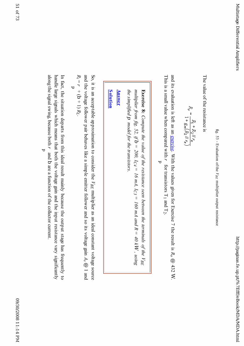
fig. 5
3 - E
valu
ation
of th
e VB
E m
ultip
lier ou
tpu
t resistance
The v
alue o
f the resistan
ce is
and
its evalu
ation
is left as an exercise. W
ith th
e valu
es given
for E
xercise 7 th
e result is R
o @
432
W.
This is a sm
all valu
e when
com
pared
with
rp
for tran
sistors T
1 and T
2 .
Exe
rcise 8
: Com
pute
the v
alu
e o
f the resista
nce
seen b
etween
the term
inals
of th
e V
BE
multip
lier from
fig. 5
2, if b
= 2
00, IC
4 = 1
6 m
A, IC
3 = 1
60
mA
and
R =
40
kW , u
sing
the sim
plified
p m
odel fo
r the tra
nsisto
rs.
An
swe
r
Solu
tion
So, it is an
acceptab
le app
roxim
ation
to co
nsid
er the V
BE
multip
lier as an id
eal constan
t voltage so
urce
and
the v
oltage fo
llow
er pair b
ehav
es like a sim
ple em
itter follo
wer an
d so
its voltage gain
Av @
1 an
d
Ri =
rp
+ (b
+ 1
) RL.
In fact, th
e situ
ation
dep
arts fro
m th
is id
eal result m
ainly
becau
se th
e o
utp
ut stage
has
frequen
tly to
han
dle
large sign
als w
hich
mean
s th
at both
the v
oltage
gain an
d th
e in
put resistan
ce v
ary sign
ificantly
alon
g the sign
al swin
g, becau
se both
rp
and b
are a functio
n o
f the co
llector cu
rrent.
Multistage
Diff
ere
ntial A
mplifi
ers
http
://pagin
as.fe.u
p.p
t/%7E
fff/e
Book/M
DA
/MD
A.h
tml
51
of 7
309/3
0/2
008 1
1:1
4 P
M
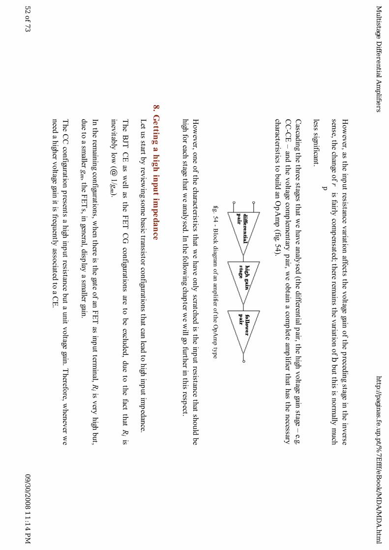
How
ever, as th
e inp
ut resistan
ce variatio
n affects th
e voltage gain
of th
e preced
ing stage in
the in
verse
sense, th
e chan
ge of r
p
is fairly co
mp
ensated
; there rem
ains th
e variatio
n o
f b b
ut th
is is norm
ally m
uch
less significan
t.
Cascad
ing th
e three stages th
at we h
ave an
alysed
(the d
ifferential p
air, the h
igh v
oltage gain
stage – e.g.
CC
-CE
– an
d th
e v
oltage
com
plem
entary
pair, w
e o
btain
a co
mp
lete am
plifier th
at has
the n
ecessary
characteristics to
build
an O
pA
mp
(fig. 54).
fig. 5
4 - B
lock
diag
ram o
f an am
plifier o
f the O
pA
mp
typ
e
How
ever, o
ne o
f the ch
aracteristics that w
e hav
e on
ly scratch
ed is th
e inp
ut resistan
ce that sh
ould
be
high
for each
stage that w
e analy
sed. In
the fo
llow
ing ch
apter w
e will go
furth
er in th
is respect.
8. G
ettin
g a
hig
h in
pu
t imp
ed
an
ce
Let u
s start by
review
ing so
me b
asic transisto
r configu
rations th
at can lead
to h
igh in
put im
ped
ance.
The
BJT
CE
as w
ell as th
e F
ET
CG
configu
ration
s are
to b
e exclu
ded
, due
to th
e fact th
at Ri is
inev
itably
low
(@ 1
/gm
).
In th
e remain
ing co
nfigu
rations, w
hen
there is th
e gate of an
FE
T as in
put term
inal, R
i is very
high
but,
due to
a smaller g
m, th
e FE
Ts, in
general, d
isplay
a smaller gain
.
The C
C co
nfigu
ration
presen
ts a high
inp
ut resistan
ce but a u
nit v
oltage gain
. Therefo
re, when
ever w
e
need
a high
er voltage gain
it is frequ
ently
associated
to a C
E.
Multistage
Diff
ere
ntial A
mplifi
ers
http
://pagin
as.fe.u
p.p
t/%7E
fff/e
Book/M
DA
/MD
A.h
tml
52 o
f 73
09/3
0/2
008 1
1:1
4 P
M

The C
E co
nfigu
ration
with
an em
itter resistor h
as also a h
igher R
i and
a moderate v
oltage gain
and
it is
som
etimes
a u
seful m
ontage
when
the
circuit
requirem
ents
are n
ot v
ery d
eman
din
g. Am
ong
the
configu
rations
we
hav
e b
een seein
g to
beh
ave
as in
put
stages w
ith m
oderate
gain, in
the
CE
configu
ration, R
i equals
rp
. Hav
ing a
differen
tial pair in
creases it to
2 rp
and
even
with
a d
ifferential
cascode it is at m
ost 4
rp . Is th
is enough
?
8.1
. Th
e C
E in
pu
t resista
nce
The v
alue o
f rp
is
which
mean
s th
at its v
alue d
epen
ds u
pon
the co
llector cu
rrent. If w
e k
eep IC
low
enough
, rp
can b
e
fairly h
igh.
Let’s tak
e as an exam
ple b
= 2
00 an
d IC
= 1
0 m
A, an
d w
e will h
ave:
If we h
ave a d
ifferential p
air in w
hich
both
transisto
rs hav
e the ab
ove static v
alues, R
id = 1
MW
.
We sh
ould
bear in
min
d th
at we h
ave alw
ays ign
ored
rm. T
hat can
be d
one if R
L is
not v
ery large.
How
ever, if w
e w
ant to
hav
e v
ery h
igh v
oltage
gain, R
L m
ay b
e v
ery large
and
rm m
ay h
ave to
be
consid
ered. T
ake th
e examp
le of fig. 5
5 to
evalu
ate Ri .
Multistage
Diff
ere
ntial A
mplifi
ers
http
://pagin
as.fe.u
p.p
t/%7E
fff/e
Book/M
DA
/MD
A.h
tml
53 o
f 73
09/3
0/2
008 1
1:1
4 P
M
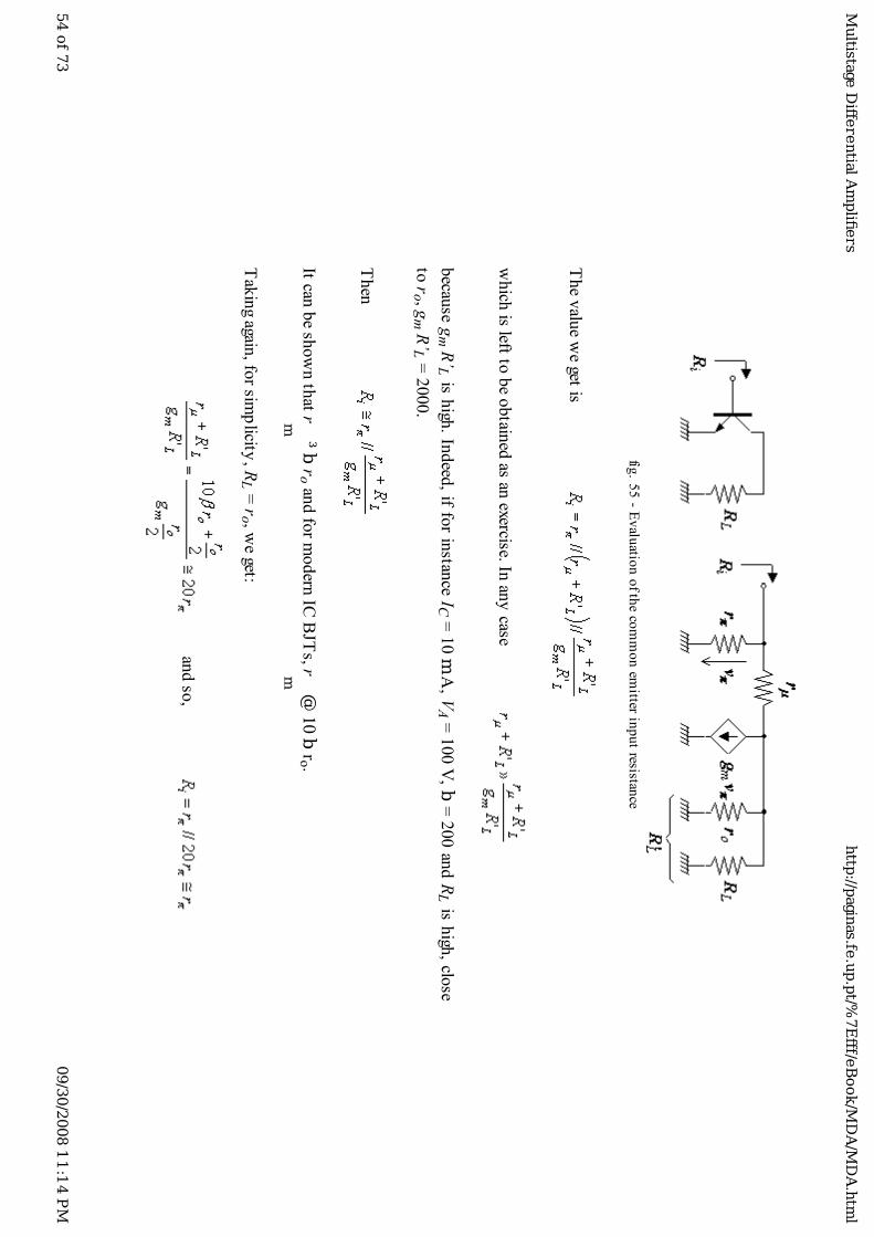
fig. 5
5 - E
valu
ation
of th
e com
mo
n em
itter inp
ut resistan
ce
The v
alue w
e get is
which
is left to b
e obtain
ed as an
exercise. In an
y case
becau
se gm
R’L
is high
. Indeed
, if for in
stance IC
= 1
0 m
A, V
A =
10
0 V
, b =
200
and
RL
is high
, close
to r
o , gm
R’L
= 2
000.
Then
It can b
e show
n th
at rm
³ b
ro an
d fo
r modern
IC B
JTs, r
m
@ 1
0 b
ro .
Tak
ing again
, for sim
plicity
, RL =
ro , w
e get:
and so
,
Multistage
Diff
ere
ntial A
mplifi
ers
http
://pagin
as.fe.u
p.p
t/%7E
fff/e
Book/M
DA
/MD
A.h
tml
54 o
f 73
09/3
0/2
008 1
1:1
4 P
M
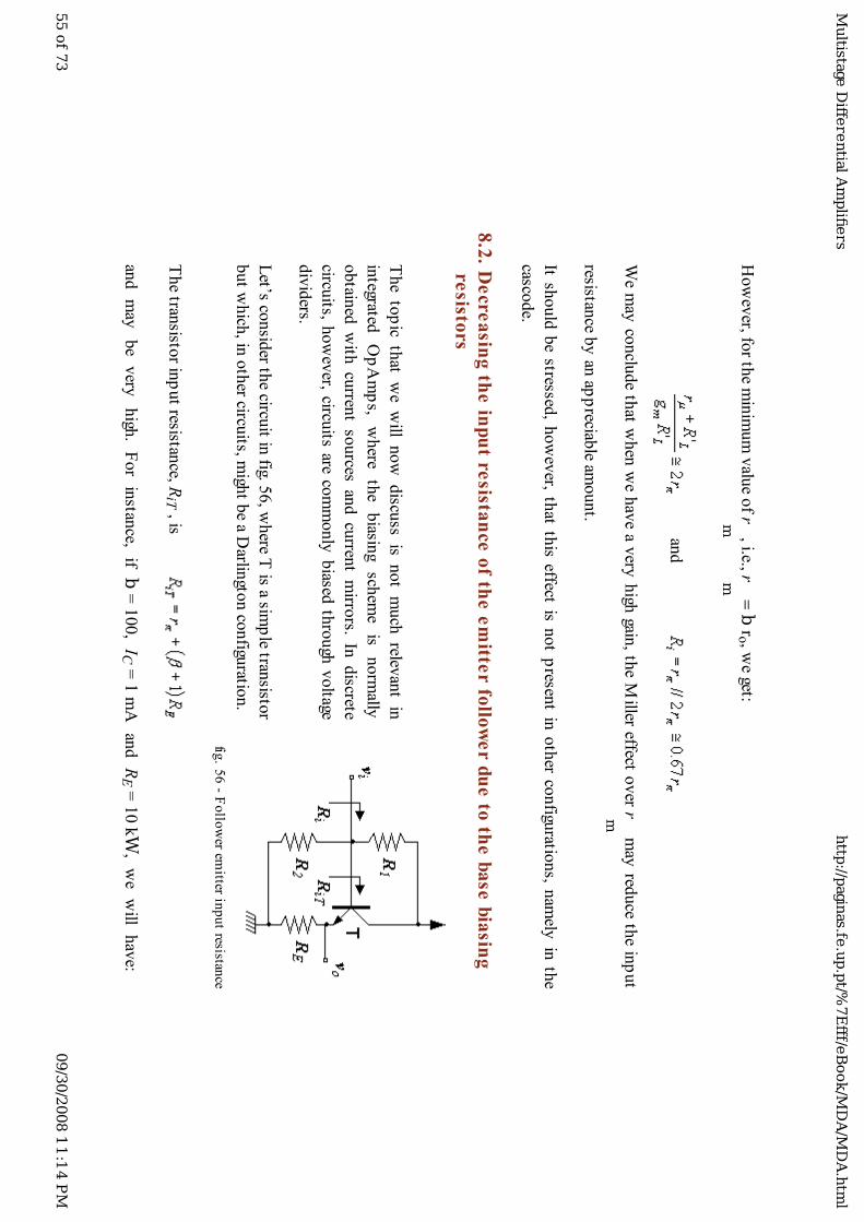
How
ever, fo
r the m
inim
um
valu
e of r
m
, i.e., rm
= b
ro , we get:
and
We m
ay co
nclu
de th
at when
we h
ave a v
ery h
igh gain
, the M
iller effect over r
m
may
redu
ce the in
put
resistance b
y an
app
reciable am
oun
t.
It should
be stressed
, how
ever, th
at this
effect is n
ot p
resent in
oth
er configu
rations, n
amely
in th
e
cascode.
8.2
. De
crea
sing
the
inp
ut re
sistan
ce o
f the
em
itter fo
llow
er d
ue
to th
e b
ase
bia
sing
resisto
rs
The
top
ic th
at w
e w
ill now
discu
ss is
not m
uch
relevan
t in
integrated
Op
Am
ps, w
here
the
biasin
g sch
eme
is n
orm
ally
obtain
ed w
ith cu
rrent so
urces
and
curren
t mirro
rs. In d
iscrete
circuits, h
ow
ever, circu
its are
com
monly
biased
thro
ugh
voltage
div
iders.
Let’s co
nsid
er the circu
it in fig. 5
6, w
here T
is a simp
le transisto
r
but w
hich
, in o
ther circu
its, migh
t be a D
arlingto
n co
nfigu
ration.
fig. 5
6 - F
ollo
wer em
itter inp
ut resistan
ce
The tran
sistor in
put resistan
ce, RiT
, is
and
may
be
very
high
. For in
stance, if
b =
100
, IC =
1 m
A an
d R
E =
10
kW, w
e w
ill hav
e:
Multistage
Diff
ere
ntial A
mplifi
ers
http
://pagin
as.fe.u
p.p
t/%7E
fff/e
Book/M
DA
/MD
A.h
tml
55 o
f 73
09/3
0/2
008 1
1:1
4 P
M

How
ever, th
e “real” in
put resistan
ce for th
e circuit is:
which
mean
s that to
hav
e Ri @
RiT
, we h
ave to
cho
ose R
B >
> R
iT . If, fo
r instan
ce, RB =
10 M
W, R
1
and R
2 had
to b
e extremely
large and
the T
hév
enin
vo
ltage
wou
ld h
ave q
uite an
unusu
al valu
e!
Let’s
now
consid
er the circu
it of fig. 5
7(a) as
well as, in
fig. 57(b
), its sm
all signal eq
uiv
alent, w
here
RB =
R1 // R
2 .
fig. 5
7 - F
ollo
wer em
itter with
bo
otstrap
efect; (a) simp
lified sch
ematic;
(b) sm
all sign
al equ
ivalen
t
Multistage
Diff
ere
ntial A
mplifi
ers
http
://pagin
as.fe.u
p.p
t/%7E
fff/e
Book/M
DA
/MD
A.h
tml
56 o
f 73
09/3
0/2
008 1
1:1
4 P
M

Ap
ply
ing
the
Miller’s
theo
rem to
R3
we
get the resu
lt dep
icted in
fig. 58, w
here
Av
is th
e v
oltage
gain, sligh
tly sm
aller th
an
one, i.e.,
.
Therefo
re
will
be
very
high
and R
i @ R
iT.
fig. 5
8 - A
pp
lyin
g th
e Miller’s th
eorem
to th
e fig. 5
7 (b
) schem
atic
This effect, w
hen
Av ®
+1, is k
now
n as b
oo
tstrap.
It should
also b
e noted
that th
e valu
e of th
e gain an
d th
e inp
ut resisto
r should
take in
to acco
unt th
at the
effective em
itter load
is not o
nly
RE, b
ut also
RB
and
. T
his last v
alue is also
very
high
and ... n
egative!
Let’s
now
recall that w
hen
we h
ave th
e p
arallel of R
, a fin
ite an
d p
ositiv
e resistan
ce, with
R’, w
hich
may
vary
from
‑¥ to
+¥
, its valu
e varies acco
rdin
g to fig. 5
9.
Multistage
Diff
ere
ntial A
mplifi
ers
http
://pagin
as.fe.u
p.p
t/%7E
fff/e
Book/M
DA
/MD
A.h
tml
57 o
f 73
09/3
0/2
008 1
1:1
4 P
M
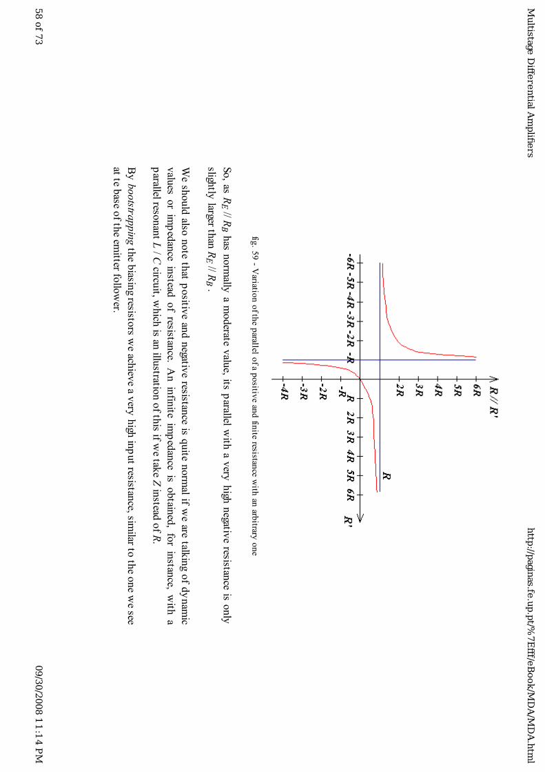
fig. 5
9 - V
ariation
of th
e parallel o
f a po
sitive an
d fin
ite resistance w
ith an
arbitrary
on
e
So, as
RE // R
B h
as n
orm
ally a
mod
erate v
alue, its
parallel w
ith a
very
high
negativ
e resistan
ce is
only
slightly
larger than
RE
// RB .
We sh
ould
also n
ote
that p
ositiv
e an
d n
egative resistan
ce is
quite
norm
al if we are
talkin
g o
f dy
nam
ic
valu
es o
r imp
edan
ce in
stead o
f resistance. A
n in
finite
imp
edan
ce is
obtain
ed, fo
r instan
ce, with
a
parallel reso
nan
t L / C
circuit, w
hich
is an illu
stration
of th
is if we tak
e Z in
stead o
f R.
By
bootstra
ppin
g th
e biasin
g resistors w
e achiev
e a very
high
inp
ut resistan
ce, similar to
the o
ne w
e see
at te base o
f the em
itter follo
wer.
Multistage
Diff
ere
ntial A
mplifi
ers
http
://pagin
as.fe.u
p.p
t/%7E
fff/e
Book/M
DA
/MD
A.h
tml
58 o
f 73
09/3
0/2
008 1
1:1
4 P
M
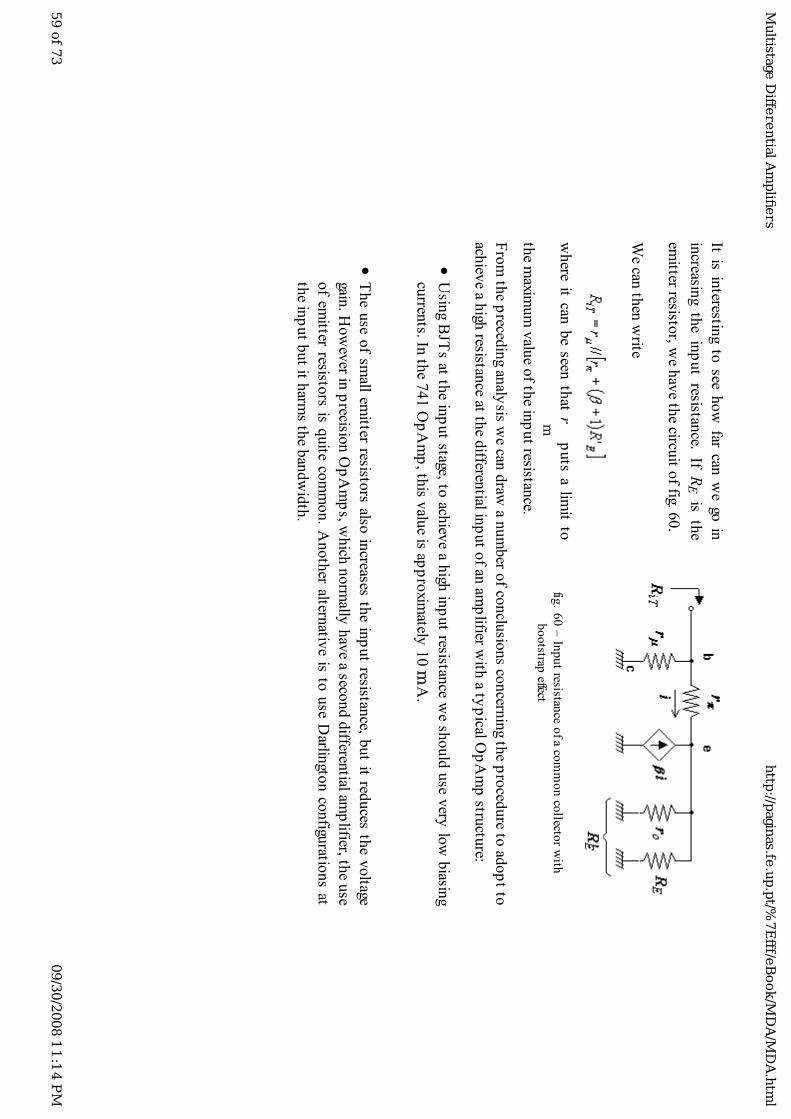
It is in
teresting to
see h
ow
far can w
e go
in
increasin
g th
e in
put resistan
ce. If R
E is
the
emitter resisto
r, we h
ave th
e circuit o
f fig. 60
.
We can
then
write
where
it can b
e seen
that r
m
puts
a lim
it to
the m
aximum
valu
e of th
e inp
ut resistan
ce.
fig. 6
0 –
Inp
ut resistan
ce of a co
mm
on
collecto
r with
bo
otstrap
effect
Fro
m th
e preced
ing an
alysis w
e can d
raw a n
um
ber o
f conclu
sions co
ncern
ing th
e pro
cedure to
adop
t to
achiev
e a high
resistance at th
e differen
tial inp
ut o
f an am
plifier w
ith a ty
pical O
pA
mp
structu
re:
Usin
g BJT
s at the in
put stage, to
achiev
e a high
inp
ut resistan
ce we sh
ou
ld u
se very
low
biasin
g
curren
ts. In th
e 741 O
pA
mp
, this v
alue is ap
pro
ximately
10 m
A.
The u
se o
f small em
itter resistors
also in
creases th
e in
put resistan
ce, but it red
uces
the v
oltage
gain. H
ow
ever in
precisio
n O
pA
mp
s, which
no
rmally
hav
e a second
differen
tial amp
lifier, the u
se
of em
itter resistors
is q
uite
com
mon. A
noth
er alternativ
e is
to u
se D
arlingto
n co
nfigu
rations at
the in
put b
ut it h
arms th
e ban
dw
idth
.
Multistage
Diff
ere
ntial A
mplifi
ers
http
://pagin
as.fe.u
p.p
t/%7E
fff/e
Book/M
DA
/MD
A.h
tml
59 o
f 73
09/3
0/2
008 1
1:1
4 P
M
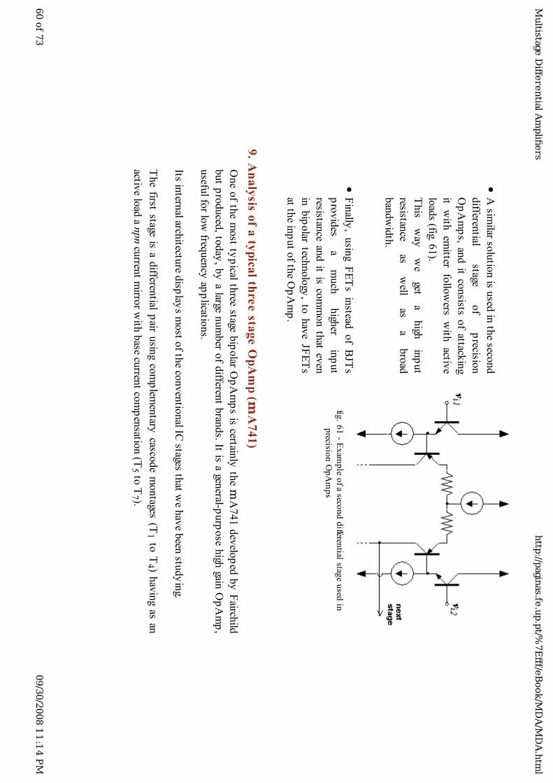
A sim
ilar solu
tion
is used
in th
e secon
d
differen
tial
stage
of
p
recision
Op
Am
ps, an
d it co
nsists
of attack
ing
it w
ith em
itter fo
llow
ers w
ith activ
e
load
s (fig. 61).
This
w
ay
we
get
a
high
in
pu
t
resistance
as
w
ell
as
a
bro
ad
ban
dw
idth
.
Fin
ally, u
sing
FE
Ts
instead
of B
JTs
pro
vid
es
a
much
high
er
inp
ut
resistance
and
it is co
mm
on
that ev
en
in b
ipolar tech
nolo
gy, to
hav
e JF
ET
s
at the in
put o
f the O
pA
mp
.
fig. 6
1 - E
xam
ple o
f a secon
d d
ifferential stag
e used
in
precisio
n O
pA
mp
s
9. A
na
lysis o
f a ty
pica
l thre
e sta
ge
Op
Am
p (m
A7
41
)
One o
f the m
ost ty
pical th
ree stage
bip
olar O
pA
mp
s is
certainly
the m
A741
dev
elop
ed b
y F
airchild
but p
roduced
, today
, by
a large nu
mber o
f differen
t bran
ds. It is a gen
eral-purp
ose h
igh gain
Op
Am
p,
usefu
l for lo
w freq
uen
cy ap
plicatio
ns.
Its intern
al architectu
re disp
lays m
ost o
f the co
nven
tional IC
stages that w
e hav
e been
study
ing.
The first stage
is a
differen
tial pair u
sing co
mp
lemen
tary casco
de m
ontages
(T1 to
T4 ) h
avin
g as
an
active lo
ad a n
pn cu
rrent m
irror w
ith b
ase curren
t com
pen
sation (T
5 to T
7 ).
Multistage
Diff
ere
ntial A
mplifi
ers
http
://pagin
as.fe.u
p.p
t/%7E
fff/e
Book/M
DA
/MD
A.h
tml
60 o
f 73
09/3
0/2
008 1
1:1
4 P
M

fig. 6
2 –
Intern
al schem
atic of th
e mA
74
1 O
pA
mp
The C
C-C
B casco
de co
nfigu
ration p
rovid
es a large ban
dw
idth
with
small in
put cap
acitance.
The in
put resistan
ce is
also h
igher (ap
pro
ximately
the d
ouble) th
an w
hat w
ou
ld resu
lt from
a sim
ple
differen
tial pair w
ith id
entical b
ias curren
ts.The in
termed
iate stage uses a C
C-C
E m
ontage (T
16 to
T1
7 )
hav
ing h
igh in
put resistan
ce, high
gain an
d a go
od
frequen
cy resp
onse. T
he 3
0 p
F cap
acitor co
nnected
betw
een in
put an
d o
utp
ut o
f this
stage p
rovid
es, as w
ill be
seen later o
n, a
Miller (p
ole
splittin
g)
com
pen
sation, gu
aranty
ing an
unco
nditio
nal stab
ility.
Multistage
Diff
ere
ntial A
mplifi
ers
http
://pagin
as.fe.u
p.p
t/%7E
fff/e
Book/M
DA
/MD
A.h
tml
61
of 7
309/3
0/2
008 1
1:1
4 P
M

The o
utp
ut stage
has
the ad
equate
high
inp
ut resistan
ce an
d lo
w o
utp
ut o
ne as
well as
good
curren
t
source an
d sin
k cap
acity.
In th
is way
, the fu
ndam
ental cell o
f this stage is th
e emitter fo
llow
er com
plem
entary
pair (T
14 to
T2
0 )
with
crosso
ver d
istortio
n co
mp
ensatio
n (T
18 , T
19 an
d R
10 ). T
his
stage is
preced
ed b
y an
oth
er single
transisto
r CE
(T2
3 ) that is u
sed as a b
uffer b
etween
the seco
nd
and th
e outp
ut stages.
Circu
it bias cu
rrents are, as u
sual, p
rovid
ed b
y a set o
f curren
t mirro
r configu
rations. T
11 , T
12 an
d R
5
establish
the v
alue o
f the cu
rrent th
at is mirro
red b
y T
10 . T
he co
nnectio
n to
the b
ase of T
3 and
T4 an
d
the T
8 -T9 m
irror, estab
lish th
e curren
ts in th
e differen
tial pair th
rough
a feedback
loop
.
The referen
ce curren
t is also m
irrored
from
T1
2 to th
e double co
llector tran
sistor T
13 w
hich
can b
e seen
as two in
dep
enden
t transisto
rs T1
3A
and T
13
B.
The 7
41
Op
Am
p h
as still a
set of extra
transisto
rs (T
15 , T
21 , T
22 an
d T
24 ) th
e ro
le o
f which
is to
pro
tect the d
evice fro
m d
amagin
g ou
tput sh
ort circu
its.
Term
inal A
and
B are
used
for o
ffset com
pen
sation
, by
mean
s o
f a 1
0 k W
poten
tiom
eter connected
betw
een A
and B
and th
e mid
dle p
oin
t connected
to
.
In th
e remain
ing an
alysis, w
e will tak
e, for all th
e transisto
rs (except T
21 , T
22 an
d T
24 th
at hav
e a three
times larger area), IS =
10
-14A
.
The to
tal area of T
3 is still the sam
e but sp
lit unev
enly
betw
een th
e two
com
ponen
ts: three fo
urth
s to
T1
3B
and th
e remain
ing fo
urth
to T
13
A. T
herefo
re
IS1
3A
= 0
.25 ´
10
-14 A
and IS
13
B =
0.7
5 ´
10
-14 A
.
Furth
ermore, w
e will tak
e, for n
pn tran
sistors,
Multistage
Diff
ere
ntial A
mplifi
ers
http
://pagin
as.fe.u
p.p
t/%7E
fff/e
Book/M
DA
/MD
A.h
tml
62 o
f 73
09/3
0/2
008 1
1:1
4 P
M
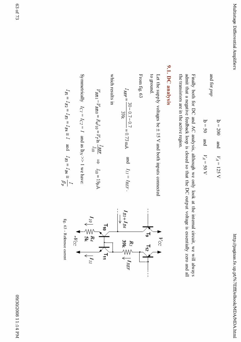
b =
200 an
d V
A =
125 V
and fo
r pnp
b =
50 an
d V
A =
50 V
Fin
ally b
oth
for D
C an
d A
C an
alysis, alth
ough
we o
nly
loo
k at th
e in
ternal circu
it, we w
ill alway
s
adm
it that a n
egative feed
back
loop
is closed
so th
at the D
C o
utp
ut v
oltage is essen
tially z
ero an
d all
the tran
sistors are in
the activ
e region.
9.1
. DC
an
aly
sis
Let th
e sup
ply
voltages b
e ± 1
5 V
and
both
inp
uts co
nnected
to gro
und.
Fro
m fig. 6
3
and I1
1 = IR
EF .
which
results in
Sy
mm
etrically IC
1 = IC
2 = I an
d as b
N >
> 1
we h
ave:
fig. 6
3 - R
eference cu
rrent
Multistage
Diff
ere
ntial A
mplifi
ers
http
://pagin
as.fe.u
p.p
t/%7E
fff/e
Book/M
DA
/MD
A.h
tml
63 o
f 73
09/3
0/2
008 1
1:1
4 P
M

Fro
m fig. 6
4 w
e may
conclu
de I9
@ I8
@ 2
I
and
and fin
ally I1 =
I2 @
I3 = I4 =
9.5
mA
.
Tran
sistors
T1
to T
4 , T8
and
T9
establish
a n
egative
feedb
ack
loop
that stab
ilises I to a v
alue ap
pro
ximately
equal to
I10 / 2
. In
fact, if for so
me reaso
n I in
creases, we’ll su
ccessively
hav
e
I8
Þ I9
and as I1
0 has a co
nstan
t valu
e
IB
3 = I
B4
Þ I3 =
I4 = I1 =
I2 = I
fig. 6
4 - B
ias curren
t of th
e differen
tial pair
The
curren
ts in
the
mirro
r that lo
ads
the
differen
tial
pair
are I5 @
I6 @ I, as
can b
e seen
in fig. 6
5 an
d
disregard
ing b
oth
IB1
6 and IB
7 .
On th
e oth
er han
d:
where
This sh
ow
s that IB
7 is indeed
very
small.
fig. 6
5 - C
urren
ts in th
e mirro
r
Multistage
Diff
ere
ntial A
mplifi
ers
http
://pagin
as.fe.u
p.p
t/%7E
fff/e
Book/M
DA
/MD
A.h
tml
64 o
f 73
09/3
0/2
008 1
1:1
4 P
M

Let’s n
ow
analy
se the seco
nd stage (fig. 6
6).
Igno
ring IB
23 ,
we h
ave I1
7 @
I13
B
and as I1
3A +
I13
B =
IRE
F an
d IS
B =
3 ´
ISA
,
I13
B @
0.7
5 IR
EF =
550 m
A =
I17 th
e result o
f which
is
and
Again
, accord
ing to
ou
r app
roxim
ations, w
e hav
e IB1
6 <<
I. fig
. 66
- Cu
rrents in
the seco
nd
stage
Multistage
Diff
ere
ntial A
mplifi
ers
http
://pagin
as.fe.u
p.p
t/%7E
fff/e
Book/M
DA
/MD
A.h
tml
65 o
f 73
09/3
0/2
008 1
1:1
4 P
M
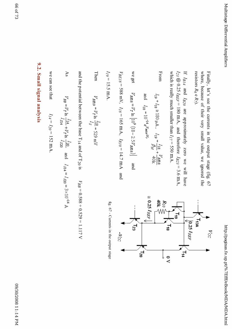
Fin
ally, let’s
see th
e cu
rrents
in th
e o
utp
ut stage
(fig. 67
where, b
ecause
of th
eir v
ery sm
all valu
e, we
igno
red th
e
resistors R
6 e R7 ).
If IB
14
and
IB2
0 are
app
roxim
ately z
ero w
e w
ill hav
e
I23 @
0.2
5 IR
EF =
180
mA
, and
therefo
re IB
23 =
3.6
mA
,
which
is really m
uch
smaller th
an I1
7 = 5
50 m
A.
Fro
m
we get
and
VB
E1
8 = 5
88 m
V, I1
8 = 1
65 m
A, IR
10 =
14.7
mA
and
I19 =
15.5
mA
. fig
. 67
- Cu
rrents in
the o
utp
ut stag
e
Then
and th
e poten
tial betw
een th
e base T
14 an
d o
f T2
0 is VB
B =
0.5
88 +
0.5
29 =
1.1
17 V
As
we can
see that I1
4 = I2
0 = 1
52 m
A.
9.2
. Sm
all sig
na
l an
aly
sis
Multistage
Diff
ere
ntial A
mplifi
ers
http
://pagin
as.fe.u
p.p
t/%7E
fff/e
Book/M
DA
/MD
A.h
tml
66 o
f 73
09/3
0/2
008 1
1:1
4 P
M
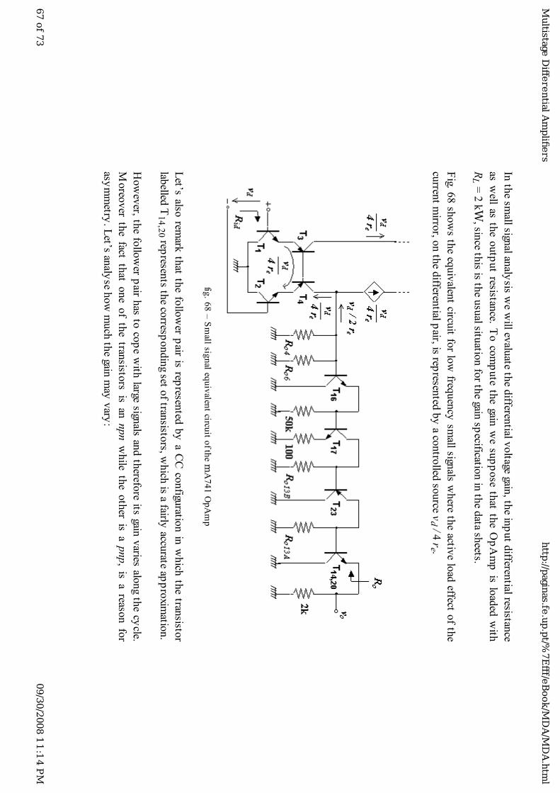
In th
e small sign
al analy
sis we w
ill evalu
ate the d
ifferential v
oltage gain
, the in
put d
ifferential resistan
ce
as w
ell as th
e o
utp
ut resistan
ce. To
com
pute
the gain
we su
pp
ose
that th
e O
pA
mp
is lo
aded
with
RL =
2 kW
, since th
is is the u
sual situ
ation fo
r the gain
specificatio
n in
the d
ata sheets.
Fig. 6
8 sh
ow
s the eq
uiv
alent circu
it for lo
w freq
uen
cy sm
all signals w
here th
e active lo
ad effect o
f the
curren
t mirro
r, on th
e differen
tial pair, is rep
resented
by
a con
trolled
source v
d / 4 r
e .
fig. 6
8 –
Sm
all sign
al equ
ivalen
t circuit o
f the m
A7
41
Op
Am
p
Let’s
also rem
ark th
at the fo
llow
er pair is
represen
ted b
y a
CC
configu
ration
in w
hich
the tran
sistor
labelled
T1
4,2
0 represen
ts the co
rrespondin
g set of tran
sistors, w
hich
is a fairly accu
rate app
roxim
ation.
How
ever, th
e follo
wer p
air has to
cop
e with
large signals an
d th
erefore its gain
varies alo
ng th
e cycle.
Moreo
ver th
e fact th
at one
of th
e tran
sistors
is an
npn
while
the
oth
er is a
pnp
, is a
reason
for
asym
metry
. Let’s an
alyse h
ow
much
the gain
may
vary
:
Multistage
Diff
ere
ntial A
mplifi
ers
http
://pagin
as.fe.u
p.p
t/%7E
fff/e
Book/M
DA
/MD
A.h
tml
67 o
f 73
09/3
0/2
008 1
1:1
4 P
M
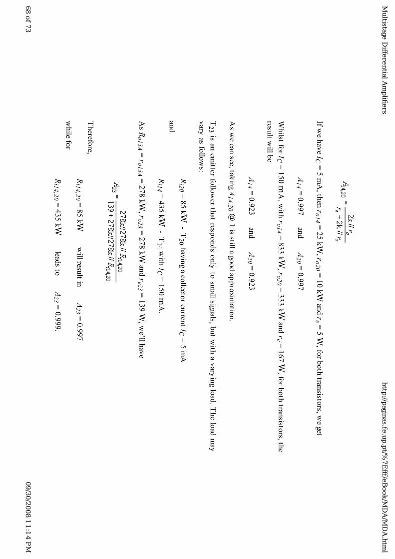
If we h
ave IC
= 5
mA
, then
ro
14 =
25 kW
, ro
20 =
10 kW
and r
e = 5
W, fo
r both
transisto
rs, we get
A1
4 = 0
.997 an
d A
20 =
0.9
97
Whilst fo
r IC =
150 m
A, w
ith r
o1
4 = 8
33 kW
, ro
20 =
333 kW
and
re =
167 W
, for b
oth
transisto
rs, the
result w
ill be
A1
4 = 0
.923 an
d A
20 =
0.9
23
As w
e can see, tak
ing A
14
,20 @
1 is still a go
od ap
pro
ximatio
n.
T2
3 is
an em
itter follo
wer th
at responds o
nly
to sm
all signals, b
ut w
ith a
vary
ing lo
ad. T
he lo
ad m
ay
vary
as follo
ws:
Ri2
0 = 8
5 kW
- T2
0 hav
ing a co
llector cu
rrent IC
= 5
mA
and
Ri1
4 = 4
35 kW
- T1
4 with
IC =
15
0 m
A.
As R
o1
3A =
ro
13
A =
27
8 kW
, ro
23 =
278 kW
and r
e23 =
139 W
, we’ll h
ave
Therefo
re,
Ri1
4,2
0 = 8
5 kW
will resu
lt in A
23 =
0.9
97
while fo
r
Ri1
4,2
0 = 4
35 kW
leads to
A2
3 = 0
.999.
Multistage
Diff
ere
ntial A
mplifi
ers
http
://pagin
as.fe.u
p.p
t/%7E
fff/e
Book/M
DA
/MD
A.h
tml
68 o
f 73
09/3
0/2
008 1
1:1
4 P
M

Again
A2
3 @ 1
is a good ap
pro
ximatio
n.
The lim
iting situ
ations are
Ri2
3 = 5
1 (1
39+
139k//8
5k
) = 2
.70 M
W
and
Ri2
3 = 5
1 (1
39+
139k//4
35
k) =
5.4
0 M
W
Let’s tak
e the sm
allest valu
e that so
meh
ow
com
pen
sates for th
e unit gain
app
roxim
ation.
For T
17 , th
at is a CE
with
emitter resistan
ce configu
ration,
where R
o1
3B =
ro
13
B =
90.9
kW an
d r
e17 =
45 W
.
To co
mp
ute th
e resistance R
o1
7 , we n
eed th
e resistance R
o1
6 and, to
com
pute th
is one, R
o4 an
d R
o6 .
To
com
pute
Ro
4 , the b
ase n
ode o
f T3 an
d T
4 is
con
sidered
as a
virtu
al ground. T
his
is o
nly
possib
le
once th
e differen
tial gain is b
eing co
nsid
ered.
So, tak
ing in
to acco
un
t that g
m4 =
38
0 m
A/V
, rp
4
= 1
32
kW an
d r
o4 =
5.2
6
MW
,
fig. 69 sh
ow
s how
, by
stepw
ise circuit tran
sform
ations, w
e get:
Ro
4 = 5
M26+
5M
13+
2k57
@ 1
0.4
MW
Multistage
Diff
ere
ntial A
mplifi
ers
http
://pagin
as.fe.u
p.p
t/%7E
fff/e
Book/M
DA
/MD
A.h
tml
69 o
f 73
09/3
0/2
008 1
1:1
4 P
M

fig. 6
9 - E
valu
ation
of th
e ou
tpu
t resistance R
o4
The v
alue o
f Ro
6 can again
be ev
aluated
in th
e same w
ay. In
fact, the b
ase circuit resistan
ce of T
6 , i.e.
the resistan
ce o
f the extern
al circuit is
only
19
W (co
mpute
this
valu
e a
s a
n exercise), w
hich
is v
ery
small w
hen
com
pared
to rp
6 . S
o, sin
ce gm
6 = 3
80
mA
/V, rp
6 =
526
kW an
d r
o6
= 1
3.2
MW
,
it results th
at
Ro
6 = 1
8.2
MW
.
We can
now
com
pute R
o1
6 , which
is the o
utp
ut resistan
ce of a C
C, w
ith a b
ase resistance R
o4 // R
o6 an
d
rp16
= 3
09 kW
:
Fin
ally, to
com
pute R
o1
7 , takin
g into
accoun
t that
gm
17 =
22 m
A/V
, rp17 =
9.0
9 kW
and r
o1
7 = 2
27 kW
,
Multistage
Diff
ere
ntial A
mplifi
ers
http
://pagin
as.fe.u
p.p
t/%7E
fff/e
Book/M
DA
/MD
A.h
tml
70 o
f 73
09/3
0/2
008 1
1:1
4 P
M
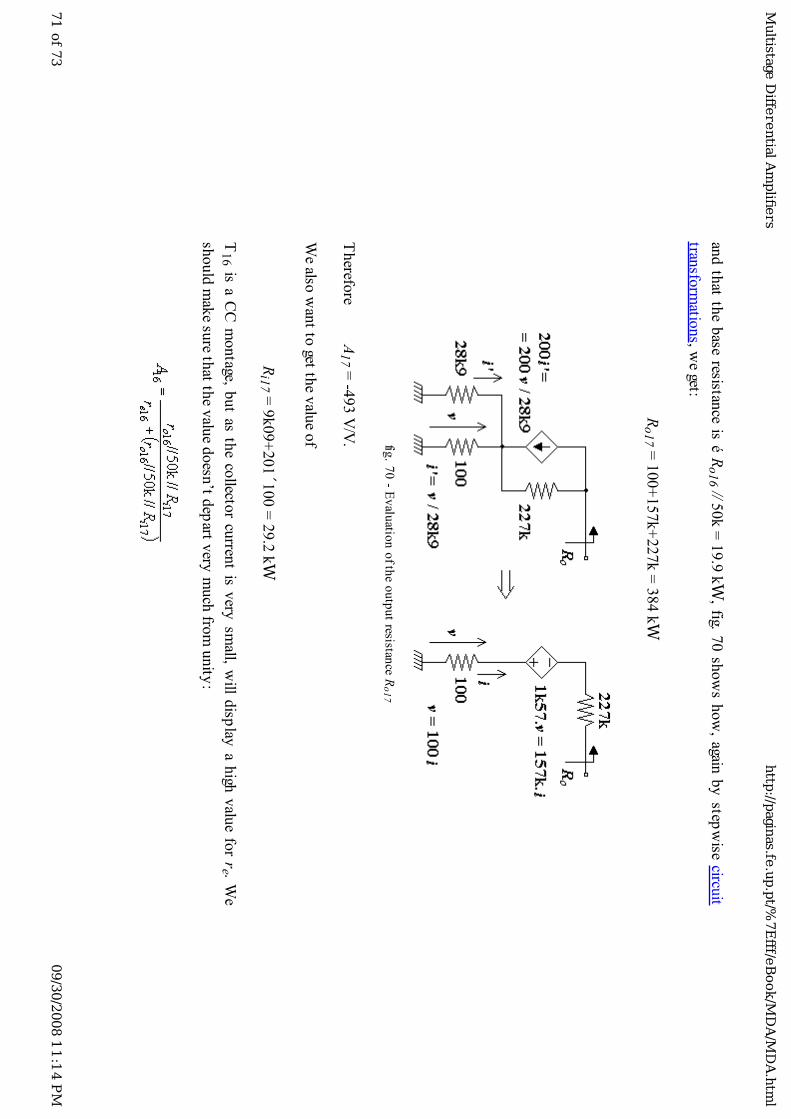
and
that th
e b
ase resistan
ce is
é R
o1
6 // 50k
= 1
9.9
kW, fig. 7
0 sh
ow
s h
ow
, again b
y step
wise
circuit
transfo
rmatio
ns, w
e get:
Ro
17 =
100+
157k
+227k =
384 kW
fig. 7
0 - E
valu
ation
of th
e ou
tpu
t resistance R
o1
7
Therefo
re A1
7 = -4
93 V
/V.
We also
wan
t to get th
e valu
e of
Ri1
7 = 9
k09+
20
1´100 =
29.2
kW
T1
6 is
a C
C m
ontage, b
ut as
the co
llector cu
rrent is
very
small, w
ill disp
lay a
high
valu
e fo
r re . W
e
shou
ld m
ake su
re that th
e valu
e doesn
’t dep
art very
much
from
unity
:
Multistage
Diff
ere
ntial A
mplifi
ers
http
://pagin
as.fe.u
p.p
t/%7E
fff/e
Book/M
DA
/MD
A.h
tml
71
of 7
309/3
0/2
008 1
1:1
4 P
M

where r
o1
6 = 7
.72 M
W an
d r
e16 =
1.5
4 kW
,
therefo
re A1
6 = 0
.923.
The in
put resistan
ce is:
Ri1
6 = 2
01 [1
k5
4+
(7M
72
//50k//2
9k2)] =
4.0
0 M
W
Fin
ally, fo
r the d
ifferential p
air we h
ave:
where r
e = 2
.63 kW
(app
roxim
ately co
mm
on to
T1 –
T4 ).
It results th
at A1 =
-474 V
/V
and fin
ally
Ad =
-474 ´
0.9
23 ´
(-493
) = -2
16
000 V
/V.
To co
mp
ute R
id is trivial. R
eportin
g to fig. 6
8, w
e can see th
at
Rid =
4 (b
N +
1) r
e = 2
.1 M
W.
On
the o
ther h
and, co
mp
utin
g Ro , i.e., th
e outp
ut resistan
ce of th
e com
plem
entary
sym
metry
follo
wer
pair, can
only
be o
btain
ed as
an av
erage v
alue. In
fact, as th
e co
mp
lemen
tary p
air work
s w
ith large
signals
the
outp
ut resistan
ce w
ill dep
end
up
on
wh
ich tran
sistor is
conductin
g as
well as
up
on
its
curren
t.
Multistage
Diff
ere
ntial A
mplifi
ers
http
://pagin
as.fe.u
p.p
t/%7E
fff/e
Book/M
DA
/MD
A.h
tml
72 o
f 73
09/3
0/2
008 1
1:1
4 P
M

If T2
0 is sup
ply
ing th
e curren
t
where
As r
o1
8 is very
small co
mp
ared to
ro
13
A (2
78 kW
), we w
ill hav
e
Ro =
re2
0 + 3
4 +
27
The v
alue o
f re2
0 dep
ends critically
on th
e curren
t.
For IC
= 1
50 m
A r
e = 1
67 W
while fo
r IC =
5 m
A r
e = 5
W, as seen
abo
ve.
Therefo
re, the v
alue can
vary
betw
een 6
6 an
d 2
28 W
. The d
ata sheets sp
ecify th
e valu
e 75 W
.
free
hit c
ou
nte
rs
Multistage
Diff
ere
ntial A
mplifi
ers
http
://pagin
as.fe.u
p.p
t/%7E
fff/e
Book/M
DA
/MD
A.h
tml
73 o
f 73
09/3
0/2
008 1
1:1
4 P
M