Embed Size (px)
Citation preview

Multi-Layer Ceramic Capacitors:
Why and How They Fail
Property of Passive Plus, Inc.
1 PPI

• MLCC materials and processes
• Lifetime limitations of materials
• Manufacturing shortcomings and defects
• When Bad Things Happen to Good Customers: Mishandling and design inadequacies
• Reliability models and testing
PPI 2 Property of Passive Plus, Inc.

Multi-Layer Ceramic Capacitor (MLCC)
PPI 3 Property of Passive Plus, Inc.

MLCC Mounted on Microstrip
PPI 4
Fig. 2. Vertically mounted multilayer chip capacitor
on microstrip
(top view "through"
dielectric cover layer)
microstrip
substrate
trace
capacitor
Section R-RR
R
termination
Features: (1) A ceramic brick with interleaved metallic electrodes (2) Soldered across a gap in microstrip center conductor (shown) or extending from center conductor to ground plane (not shown) (2) Shown oriented with electrodes vertical to substrate
Property of Passive Plus, Inc.

Design Includes Tradeoffs Among Many Factors
• Selection of materials – In manufacture of MLCC: dielectrics, electrode metal inks,
termination metallization
– In subsequent use and handling by customer: RoHS compliance, solderability, re-usability, marking requirements
• Electrical Requirements – Meeting all specifications on capacitance, tolerance, working
voltage, temperature variation, loss at operating frequency, magnetic properties, reliability, etc.
• Mechanical Requirements – Physical size, lead pull strength, bending moment, permeability
to solvents, etc.
PPI 5
Property of Passive Plus, Inc.

MLCC Fabrication Processes and Materials
• Tape-based process – Magnesium titanate dielectric,
typical temp. characteristic is P90 (cap change 90 ± 20 ppm/ 0C), e.g. PPI “P” series, but can be doped with rare earths to produce NPO (=COG) temperature characteristic (cap change ± 30 ppm/ 0C), e.g. PPI “C” series
– Barium titanate dielectric, e.g. PPI “N” series; can be doped to produce X7R characteristic: ± 15% cap change, max. from -54 to +100 0C, , e.g. PPI “X” series (X7R)
• “Wet” process – Can achieve much higher
capacitance values than tape-based processes (thinner dielectric layers), but
– Typically more loss at RF frequencies than tape-based capacitors
– Can be doped to produce NPO, X7R, Y5Z, etcetera temperature characteristics
PPI Property of Passive Plus, Inc.
6

High-Fire and Low-fire Ceramics
• High-Fire
– Sinters at ≈1350 0C
– Palladium or platinum electrodes
– Pd bulk resistivity = 11 x 10-6 ohm-cm.
– Example: PPI “C” and “P” series
• Low-fire
– Sinters at 950-1050 0C
– Silver or silver/palladium electrodes
– Ag bulk resistivity = 1.62 x 10⁻⁶ ohm-cm.
– Example: PPI “N” series
Property of Passive Plus, Inc. 7 PPI

Cost Drivers - High-fire/Low-fire
– High-fire • Palladium electrodes
• High pressure - small block size
• Dual firing / diamond sawing
– Low-fire • Silver or Silver-Palladium electrodes
• Lower pressure larger block size
• Single Co-firing of ceramic + electrodes
• Dice green
Property of Passive Plus, Inc. 8 PPI
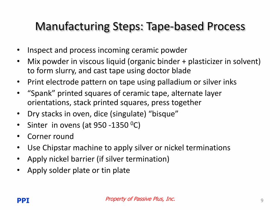
Manufacturing Steps: Tape-based Process
• Inspect and process incoming ceramic powder
• Mix powder in viscous liquid (organic binder + plasticizer in solvent) to form slurry, and cast tape using doctor blade
• Print electrode pattern on tape using palladium or silver inks
• “Spank” printed squares of ceramic tape, alternate layer orientations, stack printed squares, press together
• Dry stacks in oven, dice (singulate) “bisque”
• Sinter in ovens (at 950 -1350 0C)
• Corner round
• Use Chipstar machine to apply silver or nickel terminations
• Apply nickel barrier (if silver termination)
• Apply solder plate or tin plate
PPI 9 Property of Passive Plus, Inc.

Electrode Patterns
• Full overlap
• Floater
• Split
PPI 10 Property of Passive Plus, Inc.

More Electrode Patterns
• 60% overlap
• Multi-column
• Doubled electrodes
PPI 11 Property of Passive Plus, Inc.

MLCC Specifications and Notes (1): Tolerance Bins
Specification
• Cap value
• Tolerance
• Physical dimensions
• WVDC, DWV, WVAC
• DF and ESR
• FSR and FPR
• TCC & VCC
• Current/Power handling
• Magnetic/Non-magnetic
• Termination metallization
Tolerance bins: If you order a ±5% capacitor, you likely will receive values from (+3% - 0.05 pF) to (+5% - 0.05 pF) and -3% + 0.05 pF to (-5% + 0.05 pF) – Measurement uncertainty guard
band
PPI Property of Passive Plus, Inc.
Nominal
Value
-5% -2%
0.05pF,
Guard
Band
0.05pF
+5% +2%
0.05pF
0.05pF

MLCC Specifications and Notes (2): EIA Sizes
Specification
• Cap value
• Tolerance
• Physical dimensions
• WVDC, DWV, WVAC
• DF and ESR
• FSR and FPR
• TCC & VCC
• Current/Power handling
• Magnetic/Non-magnetic
• Termination metallization
EIA sizes are industry standards for physical dimensions and tolerances Advantages: • Provide users with a wide range of vendor choices. (Mainly for non-RF capacitors; RF capacitors can have the same physical size and capacitance, but still differ in high-frequency performance.) • Permit standardization of mounting pad layout • Permit optical orientation of capacitors • Resist “tombstoning” during soldering Disadvantages: Do not necessarily provide the best tradeoffs among parameters determining electrical performance (near-square shapes are often better)
PPI Property of Passive Plus, Inc.
13

MLCC Specifications and Notes (3): AC VOLTAGE & FSR
Specification
• Cap value
• Tolerance
• Physical dimensions
• WVDC, DWV, WVAC
• DF and ESR
• FSR and FPR
• TCC & VCC
• Current/Power handling
• Magnetic/Non-magnetic
• Termination metallization
• WVAC may be significantly lower than WVDC. Breakdown may be external or internal
• FSR in the series mode depends on substrate thickness & dielectric constant, capacitor orientation, and mounting pad dimensions
PPI Property of Passive Plus, Inc.
14
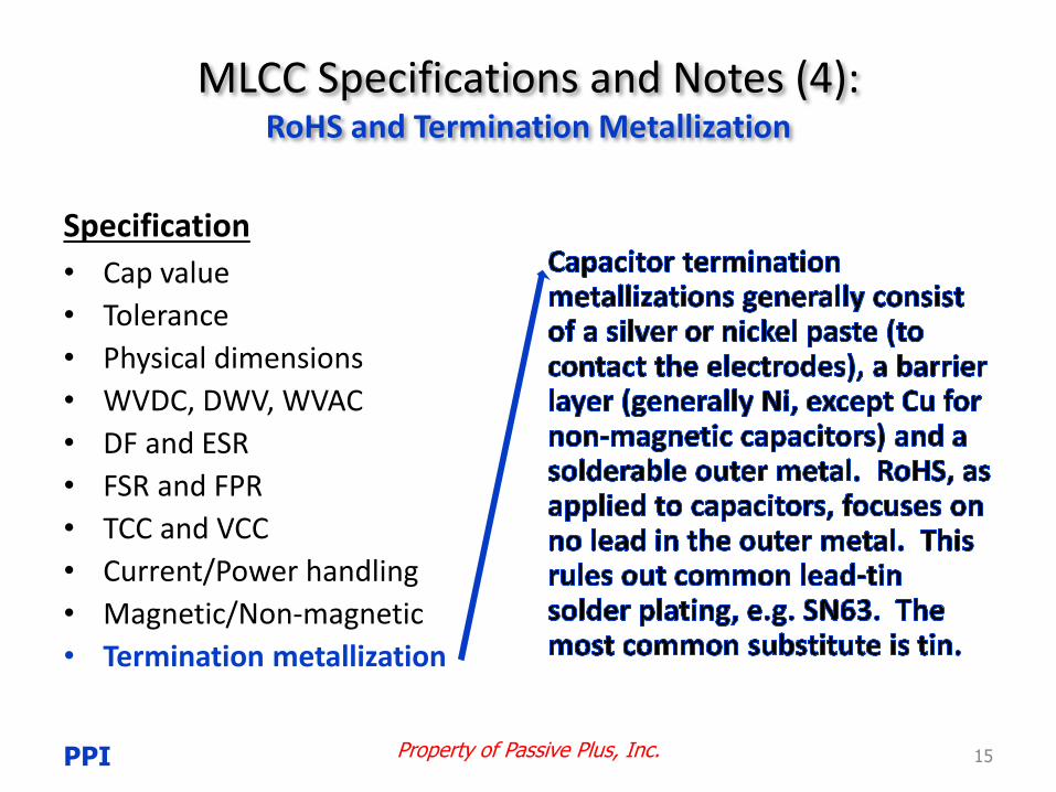
MLCC Specifications and Notes (4): RoHS and Termination Metallization
Specification
• Cap value
• Tolerance
• Physical dimensions
• WVDC, DWV, WVAC
• DF and ESR
• FSR and FPR
• TCC and VCC
• Current/Power handling
• Magnetic/Non-magnetic
• Termination metallization
PPI Property of Passive Plus, Inc.
15

Dielectric (≡ RD) and Metallic (≡ RM) Losses
Property of Passive Plus, Inc.
16
fCRD
2
tan where = dielectric loss tangent tan
f = frequency at which
RD is measured
Rm
C = capacitance value
PPI
number of electrodes, resistivity, electrode
aspect ratio, skin effect in thickness
dimension (even and odd modes within
electrodes), and skin effect (frequency-
dependent edge effect) in width dimension

Typical Equivalent Series Resistance (ESR) as a Function of Frequency
PPI Property of Passive Plus, Inc.
17
1.00
10.00
100.00
1 10 100 1000
ESR (MilliOhms)
Frequency (MHz)
Total ESR
Total ESR
Metallic Loss dominant
Dielectric Loss dominant

MLCC Failure Classifications
• Intrinsic
– Electronic disorder, lattice defects, and grain boundaries
• Extrinsic
– Voids, cracks, and de-laminations; electrode porosity; termination lift
• Customer Induced
– Electrical (current or voltage) overstress
– Thermal stress from soldering operations
– Mechanical stress (PCB flexure, pick-and-place operations)
PPI 18 Property of Passive Plus, Inc.

Intrinsic Failure in Dielectric-Metal Systems
• If a DC voltage is placed on a parallel-plate capacitor, a leakage current results; the ratio of the voltage to this leakage current is called the insulation resistance (IR), and is used as one measure of a capacitor’s integrity. – Initial leakage current results from field-induced emission of
electrons brought about by tunneling from electrodes to trap or defect states in dielectric (trap-assisted tunneling), then (a portion, thermally induced, “modified Poole–Frenkel emission”) to conduction band of dielectric + Schottky emission of Fermi level electrons directly from the electrode to the conduction band of the dielectric
– As voltage and temperature increase, leakage current increases because of oxygen vacancy migration towards cathode
– As voltage and temperature increase still further, Shottky barriers formed at cathode-ceramic interface suffer avalanche breakdown
PPI 19 Property of Passive Plus, Inc.

Perovskite Crystal Structures
PPI 20 Property of Passive Plus, Inc.

Oxygen Vacancies
• Some of the oxygen atoms escape the lattice. The vacancies left behind appear to have a charge of 2+ relative to the lattice as a whole (they are actually neutral, but occupy the location that should be held by a 2- oxygen).
• When the capacitor is in use, repeatedly charging and discharging, these vacancies can migrate as charge carriers (akin to holes in a semiconductor). The migration of oxygen vacancies to one electrode and of excess oxygen to the other results in the ceramic layer becoming similar to a pn or Schottky junction and ceasing to be effective as a capacitor.
PPI 21 Property of Passive Plus, Inc.
The pink balls are titania ions, the blue are calcium and the red, oxygen. The white ball is the migrating oxygen ion.

Vendor Processing Failure(s): Delaminations, Inclusions, Voids, Cracks
• C-SAM (scanning acoustic microscope); SEM (scanning electron microscope) after destructive physical analysis (DPA)
PPI 22 Property of Passive Plus, Inc.

Vendor Processing Failure(s): Inadequate corner rounding/termination liftoff, uneven electrode stacks, excessive electrode porosity
PPI 23 Property of Passive Plus, Inc.

Other Vendor Issues • Poor or open electrode contact to termination
(recessed electrodes)
• Design inadequacy: Outer electrode edge under termination overlap (drape)
PPI 24 Property of Passive Plus, Inc.
Not so good
Good
Good Not so good

Customer-Induced Failure: Improper Soldering
• Hand soldering principals: – To avoid heat conduction through capacitor, apply solder
first at the end with the poorest heat conduction (other, unconnected end has no heat conduction)
– Use a temperature-controlled iron set to 25-35 0C above solder liquidus temperature
– If possible, pre-heat substrate on hotplate to 150 0C
– Avoid touching iron to capacitor; touch to PC land instead.
• Reflow soldering: Follow manufacturer’s recommended time-temperature soldering profile
PPI 25 Property of Passive Plus, Inc.

Customer-Induced Failure: Cracking
PPI Property of Passive Plus, Inc.
26
• PCB distortion/warp in storage or uneven PCB design • Warped PCBs straightened after the soldering process • Vacuum pick-and-place fixtures exerting excessive force • Board test fixtures exerting excessive force • Improper soldering
Some causes of capacitor cracking:

Customer-Induced Failure: Inadequate Electrical Design
• Remember: RF Voltage capability can be quite different from DC
voltage capability and, above a certain point, typically decreases
with increasing frequency. It is also dependent on pulse width.
• Current Handling is a function of (1) heat generated in the capacitor
(=I2*ESR) and (2) heat removed from the capacitor. In general, the
temperature of the hottest point on the capacitor should not exceed
the qualifying temperature of the dielectric (typically 125 0C). Pulsed
heating may be a complex calculation depending on thermal time
constants.
• Harmonic currents can be unexpectedly high because capacitor
inductance reduces its net reactance. Further, ESRs at harmonics
may be significantly greater than the ESR at the fundamental,
resulting in substantial harmonic heating.
PPI 27 Property of Passive Plus, Inc.

Customer-Induced Failures: Proximity to Other Parts
• Voltage arc-over between two caps because of alternating polarity internal electrodes
• Voltage arc-over because of proximity to circuit board • Overheating because of proximity to hot component PPI 28
OK Possible Problem

Customer-Induced Failure: Lead Trimming
• Lead trimming shock wave
PPI 29 Property of Passive Plus, Inc.

Basic Reliability Concepts and Definitions
PPI 30 Property of Passive Plus, Inc
Probability of failure occurring before a certain time =
= Unreliability function ≡ Q(t)
Reliability function = R(t)
Failure (“hazard”) rate function = instantaneous failure frequency based on accumulated age

The Bathtub Curve
PPI 31 Property of Passive Plus, Inc.

Weibull Function
• Each portion of the bathtub curve can be modeled or described by a probability
density function known as the Weibull distribution • The most general expression of the Weibull pdf (probability density function) is
given by the three-parameter Weibull distribution expression, or:
where: β is the shape parameter, also known as the Weibull slope; η is the scale parameter; and γ is the location parameter • Frequently, the location parameter is not used, and the value for this parameter
can be set to zero. When this is the case, the pdf equation reduces to that of the two-parameter Weibull distribution.
PPI 32 Property of Passive Plus, Inc.

More (Wei)bull
PPI 33 Property of Passive Plus, Inc.
As is indicated by the plot, Weibull distributions with β< 1 have a failure rate that decreases with time, also known as infantile or early-life failures. Weibull distributions with β close to or equal to 1 have a fairly constant failure rate, indicative of useful life or random failures. Weibull distributions with β> 1 have a failure rate that increases with time, also known as wear-out failures. These comprise the three sections of the classic "bathtub curve." A mixed Weibull distribution with one subpopulation with β< 1, one subpopulation with β= 1 and one subpopulation with β> 1 would have a failure rate plot that was identical to the bathtub curve.

Formulas for Failure
• Probability of Failure at time t, F(t) = 1 – e -(t/η)β
• Mean time to failure (MTTF):
where the gamma function is
and η (V,T) = C (V/n)* e (B/T) where C and B are constants
PPI 34 Property of Passive Plus, Inc.

Voltage and Temperature Accelerating Factors
Property of Passive Plus, Inc.
35
where: t = time to failure = MTTF
V = applied DC voltage
N = voltage stress exponent = 3.0, typ.
T = absolute temperature
Ea = temperature activation energy,
typically, 1.0 eV
k = Boltzmann’s constant = 8.62 x 10⁻⁵
eV/0K
V2 (volts) V1 (volts) T1 (0C) T2 (
0C) t1/t2
100 100 25 25 1.00
100 100 25 35 3.53
150 100 25 25 3.38
200 100 125 125 8.00
100 100 125 135 2.04
211
2
2
1 11exp
TTk
E
V
V
t
t a
N
PPI
PV equation (Prokopoviz and Vaskas)
Accelerating Factors and HALT
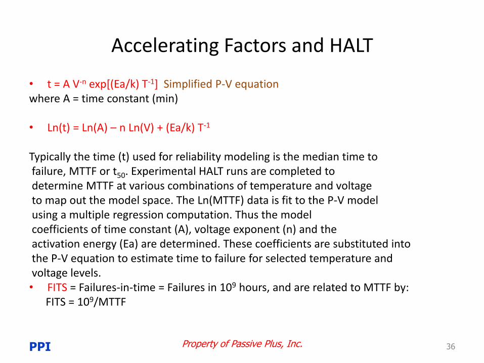
• t = A V-n exp[(Ea/k) T-1] Simplified P-V equation where A = time constant (min) • Ln(t) = Ln(A) – n Ln(V) + (Ea/k) T-1 Typically the time (t) used for reliability modeling is the median time to failure, MTTF or t50. Experimental HALT runs are completed to determine MTTF at various combinations of temperature and voltage to map out the model space. The Ln(MTTF) data is fit to the P-V model using a multiple regression computation. Thus the model coefficients of time constant (A), voltage exponent (n) and the activation energy (Ea) are determined. These coefficients are substituted into the P-V equation to estimate time to failure for selected temperature and voltage levels. • FITS = Failures-in-time = Failures in 109 hours, and are related to MTTF by: FITS = 109/MTTF
PPI 36 Property of Passive Plus, Inc.

Confidence Limits and Intervals
• Different test runs will, in general, yield a range of MTBFs
• It is possible to calculate limits that will contain the true value a certain percentage of the time
• These limits are called confidence limits, and the percentage is called the confidence level
• In the case of the exponential failure distribution -- constant failure rate -- the appropriate relation to determine confidence limits is the chi-squared (χ2) distribution
• MTTF lower limit = 2T/χ2(α/2,2n=2)
• MTTF upper limit = 2T/χ2(1-α/2, 2n)
where T is the total test time
α is the acceptable risk of error (1- desired confidence level)
n is the number of failures observed
PPI 37 Property of Passive Plus, Inc.

Salient Points
Property of Passive Plus, Inc.
38
MLCCs fail prematurely because of vendor manufacturing deficiencies, customer handling errors, and customer design inadequacies
Reliable manufacturers perform routine comprehensive testing to minimize manufacturing problems, but these do not always reveal parts that are, or will become, defective
Customers need to exercise caution and care in selection, handling, and design of circuits involving MLCCs.
PPI

Property of Passive Plus, Inc
39 PPI