Embed Size (px)
Citation preview

Journal of Instrumentation
Multi-gigabit wireless data transfer at 60 GHzTo cite this article H K Soltveit et al 2012 JINST 7 C12016
View the article online for updates and enhancements
You may also like60 GHz wireless data transfer for trackerreadout systemsmdashfirst studies and resultsS Dittmeier N Berger A Schoumlning et al
-
Design and characterisation of a screen-printed millimetre-wave flexiblemetasurface using copper ink forcommunication applicationsOluyemi P Falade Syeda Fizzah JilaniAbshir Yusuf Ahmed et al
-
Ku to V-band 4-bit MEMS phase shifterbank using high isolation SP4T switchesand DMTL structuresSukomal Dey Shiban K Koul Ajay KPoddar et al
-
Recent citationsEffects of proton irradiation on 60 GHzCMOS transceiver chip for multi-Gbpscommunication in high-energy physicsexperimentsImran Aziz et al
-
Wireless data transmission for high energyphysics applicationsSebastian Dittmeier et al
-
Feasibility studies for a wireless 60GHztracking detector readoutS Dittmeier et al
-
This content was downloaded from IP address 153199241126 on 18112021 at 1548
2012 JINST 7 C12016
PUBLISHED BY IOP PUBLISHING FOR SISSA MEDIALAB
RECEIVED June 11 2012ACCEPTED October 29 2012
PUBLISHED December 12 2012
WIT2012 mdash WORKSHOP ON INTELLIGENT TRACKERS3ndash5 MAY 2012INFN PISA ITALY
Multi-gigabit wireless data transfer at 60 GHz
HK Soltveita1 R Brennerb A Schoninga and D Wiednera
aPhysikalisches Institut Universitat HeidelbergIm Neuenheimer Feld 226 69120 Heidelberg Germany
bDepartment of Physics and Astronomy Uppsala UniversityBox 516 SE-75120 Uppsala Sweden
E-mail soltveitphysiuni-heidelbergde
ABSTRACT In this paper we describe the status of the first prototype of the 60 GHz wireless Multi-gigabit data transfer topology currently under development at University of Heidelberg using IBM130 nm SiGe HBT BiCMOS technology The 60 GHz band is very suitable for high data rate andshort distance applications One application can be a wireless multi Gbps radial data transmissioninside the ATLAS silicon strip detector making a first level track trigger feasible The wirelesstransceiver consists of a transmitter and a receiver The transmitter includes an On-Off Keying(OOK) modulator a Local Oscillator (LO) a Power Amplifier (PA) and a Band-pass Filter (BPF)The receiver part is composed of a Band-pass Filter (BPF) a Low Noise Amplifier (LNA) a doublebalanced down-convert Gilbert mixer a Local Oscillator (LO) then a BPF to remove the mixerintroduced noise an Intermediate Amplifier (IF) an On-Off Keying demodulator and a limitingamplifier The first prototype would be able to handle a data-rate of about 35 Gbps over a linkdistance of 1 m The first simulations of the LNA show that a Noise figure (NF) of 5 dB a powergain of 21 dB at 60 GHz with a 3 dB bandwidth of more than 20 GHz with a power consumption11 mW are achieved Simulations of the PA show an output referred compression point P1dB of197 dB at 60 GHz
KEYWORDS Electronic detector readout concepts (gas liquid) Analogue electronic circuitsFront-end electronics for detector readout
1Corresponding author
ccopy 2012 IOP Publishing Ltd and Sissa Medialab srl doi1010881748-0221712C12016
2012 JINST 7 C12016
Contents
1 Introduction 1
2 System architecture overview 221 Low Noise Amplifier 322 Gilbert mixer 523 Voltage controlled oscillator 524 Power amplifier 525 On-Off Keying 6
3 Link budget and channel characterization 7
4 Choice of technology 7
5 3D development 7
6 Conclusions and further work 8
1 Introduction
The data transfer rate from highly granular tracking detectors in High Energy Physics (HEP) arelimited today by the available bandwidth in the readout links This prevents the detectors to be usedfor fast triggering The bandwidth needed to read out all 1ndash2 hit clusters in the upgraded ATLASsilicon micro-strip tacker is between 50ndash100 Tbs Therefore to get the tracker to contribute tothe fast trigger decision the data transfer bandwidth from the tracker has either to be increasedfor all data to read out in real time or the quantity of the data has to be reduced by filteringthe data or a combination of the two [1] Our proposal is to read out the data radially figure 1which will help the track trigger and also reduce the latency The need for higher data rates andmore bandwidth has resulted in an increased interests in millimeter wave systems The 60 GHzunlicensed frequency band available since 2001 is of particular interest for indoor point-to-pointmulti-gigabit data transfer due to its extremely large amount of spectral bandwidth (7ndash9 GHz) Withsuch a bandwidth available and the optimum choice of modulation scheme it would be possible toachieve a data rate in the 10rsquos Gbps range and it could therefore be a suitable method to solve thedata transfer rate problem The signal transfer is Line-Of-Sight (LOS) due to indoor use and noobstacles between the layers Short and virtually interference free data transfer distance and narrowantenna beam result in secure communication Due to short distance and high carrier frequencyone obtains low power and form factor These requirements relaxe the specifications substantiallyAnother attractive feature of the 60 GHz band is the high attenuation through silicon [1] Thisisolation reduces interference to other users increasing the frequency re-use and improving the
ndash 1 ndash
2012 JINST 7 C12016
Layer A
Layer C
Layer B
Outer enclosure
~10 cm
Figure 1 Proposal of a radial readout for the tracker detector of the ATLAS experiment [1]
system capacity for short range applications We are currently working on the design of a wirelesstransceiver operating in the 60 GHz band that is capable of delivering multi-gigabit per seconddata rates and therefore it could be a potential solution to this challenge The targeted data ratefor our first prototype is 35 Gbps This paper describes the design of the wireless readout chip inIBM 130 nm SiGe Heterojunction Bipolar Transistor (HBT) BiCMOS technology with an ftfmax= 200230 GHz In section 2 the proposed transceiver architecture is presented and the differentbuilding blocks are described In section 4 the choice of technology is explained In section 5 the3D potential is explained The conclusions are presented in section 6
2 System architecture overview
The block diagram of the proposed 60 GHz transceiver chain is illustrated in figure 2 It consist ofa transmitter and a receiver part The transmitter includes a 60 GHz Voltage Controlled Oscillator(VCO) an ON-OFF Keying (OOK) modulator and a Power Amplifier (PA) In order to makethe data pass through the air it is modulated onto the carrier signal of 60 GHz The PA providesthe 60 GHz modulated signal with the required power and amplification The PA is followed by aBPF to suppress the induced broad band noise from the PA itself and carrier feedthrough productsfrom the up-convert process The filtered signal is then transmitted through the antenna Thereceiver chain is composed of a bandpass-filter a LNA a double-balanced mixer an IF amplifieran OOK demodulator and a limiting amplifier The purpose of the receiver is to detect the normallyvery small mm-wave signal and down-convert it with minimum added noise The signal from theantenna is first passed through the BPF before it reaches the LNA The purpose of the BPF is toattenuate out-of-band interferences The main function of the LNA is to amplify the weak signalwhile adding as little noise and distortion as possible The mixer down-converts the passbandsignal to a lower frequency in this case 5 GHz to make it easier for the following gain filtering
ndash 2 ndash
2012 JINST 7 C12016
MixerLNA
Antenna
Downconvert
Band-
pass
Filter
Oscillator
Low Noise
Amplifier
IF
amp
OOK
Demod
Lim
ampDout
Band-
pass
Filter
DinPA
Antenna
Oscillator
Power
Amplifier
OOK
mod
Band-
pass
Filter
Figure 2 Block diagram of the Transceiver The transmitter is shown at the top and the receiver at thebottom
and demodulation stages A bandpass-filter then follows in order to reject the superimposed noiseharmonics and mixer inter-modulated products generated in the down conversion process Thesignal is then further amplified with the use of an IF amplifier to increase the dynamic range OOKis chosen as the modulation scheme for the first prototype It eliminates the digital interface andbaseband circuitry
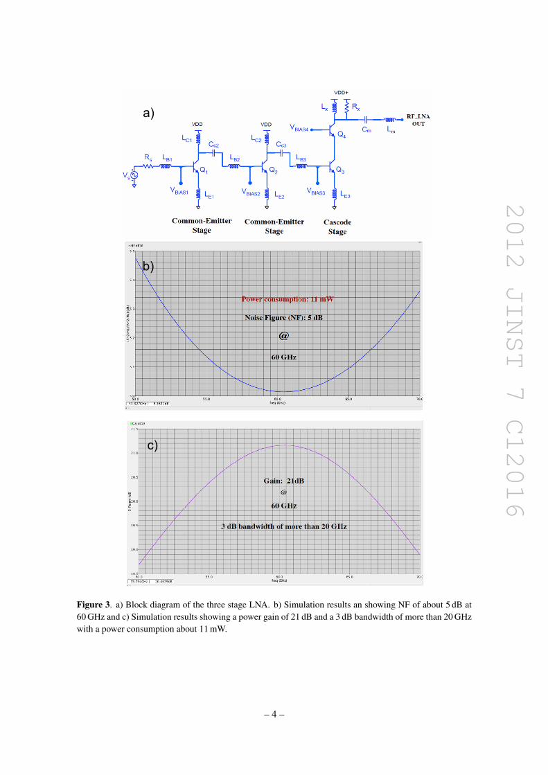
21 Low Noise Amplifier
The signal power level at the antenna below minus56 dBm show the need for low-noise and amplifi-cation The LNA plays a crucial role as the first active block in the receiver chain following theantenna its noise figure sets a lower limit on the noise figure of the entire system So the main goalof the LNA is to amplify the weak signal received on the antenna while adding as little noise as pos-sible The chosen topology for the LNA is shown in figure 3a In order to provide enough gain lownoise and isolation the LNA is implemented with a three stage cascade design For input matchingand noise optimization of the first stage the size of transistor Q1 the emitter degeneration inductorLE1 the input capacitance and the inductor are tuned simultaneously The inductively generatedemitter topology has been chosen for the two first stages due to its better gain noise figure and toimprove the linearity The two first stages are biased at minimum NF current to minimize the noisewhile the last stage provides high gain and isolation
This gives the best compromise between maximum gain and minimum NF Each stage isbiased independently For simplicity the bias network is not shown Simulations of the LNAfigure 3c give a NF of 5 dB with a power consumption of 11 mW at 60 GHz A simulated gain of21 dB with a bandwidth of 20 GHz is also achieved as seen in figure 3b
ndash 3 ndash
2012 JINST 7 C12016
a)
b)
c)
Figure 3 a) Block diagram of the three stage LNA b) Simulation results an showing NF of about 5 dB at60 GHz and c) Simulation results showing a power gain of 21 dB and a 3 dB bandwidth of more than 20 GHzwith a power consumption about 11 mW
ndash 4 ndash
2012 JINST 7 C12016
a) b)
Figure 4 A simplified block diagram of the double balanced Gilbert mixer (left) and the Voltage ControlledOscillator (right)
22 Gilbert mixer
The mixer performance has a great influence on the characteristics of the overall front end Sinceit follows the LNA the issue of linearity becomes significant because it must handle amplifiedsignals While it may seem that the issue of noise is relaxed by the LNA gain in practice mixersexhibit a high noise figure that should also be taken into account The gain of the mixer is also im-portant to compensate for the intermediate frequency filter loss and to reduce the noise contributionfrom the IF stages So in a mixer design it is always necessary to achieve a trade-off among thethree main parameters gain noise figure and linearity A double balanced Gilbert cell is chosenas a mixer figure 4a It takes the input and down-converts it to 5 GHz for easy signal processing inthe receiver Strong LO-IF feedthrough is suppressed by the double balanced mixer All the evenharmonics are cancelled All the odd harmonics are doubled It provides a reasonable gain
23 Voltage controlled oscillator
The voltage controlled oscillator (VCO) is a key component in transceivers The voltage controlledfrequency of operation is achieved by voltage dependant capacitance devices such as varactorsThe VCO provides the reference frequency to modulatedemodulate the RF signal VCOrsquos are par-ticularly sensitive to phase noise which physically represents the up-conversion of low frequency(1f) noise to RF frequency The Colpitts topology in figure 4b is chosen for low-phase noise andhigh frequency behavior For this prototype design the goal of the VCO is to have a tuning rangeof 7 GHz and a phase noise of less than minus90 dBcHz at 1 MHz
24 Power amplifier
The power amplifier is the final active block in the transmit path of the transceiver The purposeis to provide the signal with the required power level to ensure that the transmitted signal reaches
ndash 5 ndash
2012 JINST 7 C12016
a)
b)
Figure 5 A simplified block diagram of the Power Amplifier a) and simulation of its compression point b)
the receiver with the required power level In order to provide high gain which improves thePower Added Efficiency (PAE) and isolation a two stage cascode topology was chosen as shownin figure 5a The PA is biased in class AB mode to maintain high efficiency The low external baseresistance minimizes impact ionization and thus maximizes the breakdown voltage of the outputdevice Preliminary simulations of the PA gives a compression point of about 20 dBm for a input ofabout 8 dBm The input power return loss is aboutminus65 dB Since the need for extreme transmissionpower is not required in our specific design a new PA with less transmitting power (0 dBm) is underdevelopment This will reduce the power consumption of the whole system drastically since thePA is the main contributor
25 On-Off Keying
An on-off shift keying (OOK) [2] modulationdemodulation scheme will be used for the first pro-totype because of the relative low complexity of implementation and very high data rates offeredThe OOK represents the digital data as the presence as ldquoonerdquo or absence ldquozerordquo of a carrier waveOOK modulation has the advantage of allowing the transmitter to idle during the transmission ofa ldquozerordquo and therefore saving power Other advantages are the need of non-linear amplifiers im-munity to VCO phase noise and no need for DSP circuitry OOK supports data rates up to halfthe available bandwidth [2] but with an available bandwidth of 7 GHz a data rate of 35 Gbps ispossible
ndash 6 ndash
2012 JINST 7 C12016
3 Link budget and channel characterization
A link budget evaluation is mandatory to get insight into the specifications for some of the mostimportant blocks To decide the appropriate system design at 60 GHz a characterization of thechannel is done Important specifications are range limitations material propagation availableand permitted output power available bandwidth receiver sensitivity multi-path propagation andenvironmental conditions A loss from the feed-line of 4 dB the passive filters of 6 dB and a pathloss of 60 GHz signal is 68 dB for a distance of 1 meter The required SNR is 17 dB for a BERof 10minus12 A total antenna gain of 16 dBi fade-margin of 20 dB and a bandwidth of 5 GHz is hereanticipated For a maximum LOS distance of about 1 m a transmit power of about 20 dBm isrequired to fulfill these requirements
4 Choice of technology
The technology chosen must be able to fulfill requirements such as noise and linearity and at thesame time have a high production yield at a reasonable cost Considering availability cost and thelow integration level of these technologies only the two mainstream technologies CMOS and SiGeHBT BiCMOS come into question Compared to CMOS SiGe HBT transistors have less processvariability andor better yield since its performance depends on the vertical diffusion which is lessvariable than the CMOS lateral gate length higher carrier mobility constants and higher breakdownvoltages The modeling for SiGe is easier for high frequency which turns into higher probabilityfor a successful first time pass 1f noise is much lower in SiGe HBTrsquos Bipolar transistors havehigher gmI which means more gain for the same bias current which can be traded off to improvethe NF The SiGe BiCMOS technology combines both high speed HBTs with relatively highbreakdown voltage and standard CMOS transistors allowing a very high integration level Theelectrical performance has been tested after irradiation and it was concluded that the technologyis suitable for condition of the High Luminosity LHC (HL-LHC) upgrade [3] Based on thesereasons it was decided to design the 60 GHz transceiver chain in the 130 nm SiGe HBT BiCMOStechnology
5 3D development
There are some challenges with the integration of mm-wave systems on a silicon substrate in spiteof its numerous advantages One is the non optimal implementation of antenna and passives insilicon due to the high loss through the silicon substrate A natural step could be to go to 3D Thekey benefit of 3D heterogenous designs with Through Silicon Vias (TSV) is its ability to combineoptimum mature and incompatible process technologies most suitable for the specific functioneq logic memory analog and RF circuits in specialized processes This keeps development costlow minimizes risk and time TSV offer significant power savings and much better performancegains than any other means of connecting stacked die Also they do not require high drive IOssaving not only power but also die area and silicon cost TSVs enable die stacking on the waferlevel and produces hundreds of thousands of die stacks simultaneously As manufacturing tech-niques mature TSVs promise to add more cost savings further adds to the compelling technicalbenefits [4]
ndash 7 ndash
2012 JINST 7 C12016
6 Conclusions and further work
A transceiver using the 60 GHz band as a solution to the bandwidth limitation for a first level tracktrigger and to meet the requirement set by the high data rate in HEP has been proposed Individualblocks under development designed in 130 nm SiGe HBT BiCMOS have been described Firstsimulations show that reasonable noise and power levels at 60 GHz is achieved The choice oftechnology and the benefit of going 3D has been briefly discussed The first prototype of thetransceiver is forseen to be submitted mid 2013
References
[1] R Brenner and S Cheng Multigigabit wireless transfer of trigger data through millimetre wavetechnology 2010 JINST 5 C07002 in Workshop on Intelligent Trackers 2010 Lawrence BerkeleyNational Laboratory Berkeley USA 3ndash5 Feb 2010
[2] J Lee Y Chen and Y Huang A low-power low-cost fully-integrated 60-GHz transceiver system withOOK modulation and on-board antenna assembly IEEE J Solid-St Circ 45 (2010) 264
[3] M Ullan et al Evaluation of two SiGe HBT technologies for the ATLAS sLHC upgrade inProceedings of the Topical Workshop on Electronics for Particle Physics Naxos Greece15ndash19 Sep 2008 pp 111ndash115
[4] GSA Tour guide to 3D-IC design tools amp services DAC 2010httpwwwgsaglobalorgedadocsTour Guide to 3D ToolsServices FINAL 001pdf
ndash 8 ndash

2012 JINST 7 C12016
PUBLISHED BY IOP PUBLISHING FOR SISSA MEDIALAB
RECEIVED June 11 2012ACCEPTED October 29 2012
PUBLISHED December 12 2012
WIT2012 mdash WORKSHOP ON INTELLIGENT TRACKERS3ndash5 MAY 2012INFN PISA ITALY
Multi-gigabit wireless data transfer at 60 GHz
HK Soltveita1 R Brennerb A Schoninga and D Wiednera
aPhysikalisches Institut Universitat HeidelbergIm Neuenheimer Feld 226 69120 Heidelberg Germany
bDepartment of Physics and Astronomy Uppsala UniversityBox 516 SE-75120 Uppsala Sweden
E-mail soltveitphysiuni-heidelbergde
ABSTRACT In this paper we describe the status of the first prototype of the 60 GHz wireless Multi-gigabit data transfer topology currently under development at University of Heidelberg using IBM130 nm SiGe HBT BiCMOS technology The 60 GHz band is very suitable for high data rate andshort distance applications One application can be a wireless multi Gbps radial data transmissioninside the ATLAS silicon strip detector making a first level track trigger feasible The wirelesstransceiver consists of a transmitter and a receiver The transmitter includes an On-Off Keying(OOK) modulator a Local Oscillator (LO) a Power Amplifier (PA) and a Band-pass Filter (BPF)The receiver part is composed of a Band-pass Filter (BPF) a Low Noise Amplifier (LNA) a doublebalanced down-convert Gilbert mixer a Local Oscillator (LO) then a BPF to remove the mixerintroduced noise an Intermediate Amplifier (IF) an On-Off Keying demodulator and a limitingamplifier The first prototype would be able to handle a data-rate of about 35 Gbps over a linkdistance of 1 m The first simulations of the LNA show that a Noise figure (NF) of 5 dB a powergain of 21 dB at 60 GHz with a 3 dB bandwidth of more than 20 GHz with a power consumption11 mW are achieved Simulations of the PA show an output referred compression point P1dB of197 dB at 60 GHz
KEYWORDS Electronic detector readout concepts (gas liquid) Analogue electronic circuitsFront-end electronics for detector readout
1Corresponding author
ccopy 2012 IOP Publishing Ltd and Sissa Medialab srl doi1010881748-0221712C12016
2012 JINST 7 C12016
Contents
1 Introduction 1
2 System architecture overview 221 Low Noise Amplifier 322 Gilbert mixer 523 Voltage controlled oscillator 524 Power amplifier 525 On-Off Keying 6
3 Link budget and channel characterization 7
4 Choice of technology 7
5 3D development 7
6 Conclusions and further work 8
1 Introduction
The data transfer rate from highly granular tracking detectors in High Energy Physics (HEP) arelimited today by the available bandwidth in the readout links This prevents the detectors to be usedfor fast triggering The bandwidth needed to read out all 1ndash2 hit clusters in the upgraded ATLASsilicon micro-strip tacker is between 50ndash100 Tbs Therefore to get the tracker to contribute tothe fast trigger decision the data transfer bandwidth from the tracker has either to be increasedfor all data to read out in real time or the quantity of the data has to be reduced by filteringthe data or a combination of the two [1] Our proposal is to read out the data radially figure 1which will help the track trigger and also reduce the latency The need for higher data rates andmore bandwidth has resulted in an increased interests in millimeter wave systems The 60 GHzunlicensed frequency band available since 2001 is of particular interest for indoor point-to-pointmulti-gigabit data transfer due to its extremely large amount of spectral bandwidth (7ndash9 GHz) Withsuch a bandwidth available and the optimum choice of modulation scheme it would be possible toachieve a data rate in the 10rsquos Gbps range and it could therefore be a suitable method to solve thedata transfer rate problem The signal transfer is Line-Of-Sight (LOS) due to indoor use and noobstacles between the layers Short and virtually interference free data transfer distance and narrowantenna beam result in secure communication Due to short distance and high carrier frequencyone obtains low power and form factor These requirements relaxe the specifications substantiallyAnother attractive feature of the 60 GHz band is the high attenuation through silicon [1] Thisisolation reduces interference to other users increasing the frequency re-use and improving the
ndash 1 ndash
2012 JINST 7 C12016
Layer A
Layer C
Layer B
Outer enclosure
~10 cm
Figure 1 Proposal of a radial readout for the tracker detector of the ATLAS experiment [1]
system capacity for short range applications We are currently working on the design of a wirelesstransceiver operating in the 60 GHz band that is capable of delivering multi-gigabit per seconddata rates and therefore it could be a potential solution to this challenge The targeted data ratefor our first prototype is 35 Gbps This paper describes the design of the wireless readout chip inIBM 130 nm SiGe Heterojunction Bipolar Transistor (HBT) BiCMOS technology with an ftfmax= 200230 GHz In section 2 the proposed transceiver architecture is presented and the differentbuilding blocks are described In section 4 the choice of technology is explained In section 5 the3D potential is explained The conclusions are presented in section 6
2 System architecture overview
The block diagram of the proposed 60 GHz transceiver chain is illustrated in figure 2 It consist ofa transmitter and a receiver part The transmitter includes a 60 GHz Voltage Controlled Oscillator(VCO) an ON-OFF Keying (OOK) modulator and a Power Amplifier (PA) In order to makethe data pass through the air it is modulated onto the carrier signal of 60 GHz The PA providesthe 60 GHz modulated signal with the required power and amplification The PA is followed by aBPF to suppress the induced broad band noise from the PA itself and carrier feedthrough productsfrom the up-convert process The filtered signal is then transmitted through the antenna Thereceiver chain is composed of a bandpass-filter a LNA a double-balanced mixer an IF amplifieran OOK demodulator and a limiting amplifier The purpose of the receiver is to detect the normallyvery small mm-wave signal and down-convert it with minimum added noise The signal from theantenna is first passed through the BPF before it reaches the LNA The purpose of the BPF is toattenuate out-of-band interferences The main function of the LNA is to amplify the weak signalwhile adding as little noise and distortion as possible The mixer down-converts the passbandsignal to a lower frequency in this case 5 GHz to make it easier for the following gain filtering
ndash 2 ndash
2012 JINST 7 C12016
MixerLNA
Antenna
Downconvert
Band-
pass
Filter
Oscillator
Low Noise
Amplifier
IF
amp
OOK
Demod
Lim
ampDout
Band-
pass
Filter
DinPA
Antenna
Oscillator
Power
Amplifier
OOK
mod
Band-
pass
Filter
Figure 2 Block diagram of the Transceiver The transmitter is shown at the top and the receiver at thebottom
and demodulation stages A bandpass-filter then follows in order to reject the superimposed noiseharmonics and mixer inter-modulated products generated in the down conversion process Thesignal is then further amplified with the use of an IF amplifier to increase the dynamic range OOKis chosen as the modulation scheme for the first prototype It eliminates the digital interface andbaseband circuitry
21 Low Noise Amplifier
The signal power level at the antenna below minus56 dBm show the need for low-noise and amplifi-cation The LNA plays a crucial role as the first active block in the receiver chain following theantenna its noise figure sets a lower limit on the noise figure of the entire system So the main goalof the LNA is to amplify the weak signal received on the antenna while adding as little noise as pos-sible The chosen topology for the LNA is shown in figure 3a In order to provide enough gain lownoise and isolation the LNA is implemented with a three stage cascade design For input matchingand noise optimization of the first stage the size of transistor Q1 the emitter degeneration inductorLE1 the input capacitance and the inductor are tuned simultaneously The inductively generatedemitter topology has been chosen for the two first stages due to its better gain noise figure and toimprove the linearity The two first stages are biased at minimum NF current to minimize the noisewhile the last stage provides high gain and isolation
This gives the best compromise between maximum gain and minimum NF Each stage isbiased independently For simplicity the bias network is not shown Simulations of the LNAfigure 3c give a NF of 5 dB with a power consumption of 11 mW at 60 GHz A simulated gain of21 dB with a bandwidth of 20 GHz is also achieved as seen in figure 3b
ndash 3 ndash
2012 JINST 7 C12016
a)
b)
c)
Figure 3 a) Block diagram of the three stage LNA b) Simulation results an showing NF of about 5 dB at60 GHz and c) Simulation results showing a power gain of 21 dB and a 3 dB bandwidth of more than 20 GHzwith a power consumption about 11 mW
ndash 4 ndash
2012 JINST 7 C12016
a) b)
Figure 4 A simplified block diagram of the double balanced Gilbert mixer (left) and the Voltage ControlledOscillator (right)
22 Gilbert mixer
The mixer performance has a great influence on the characteristics of the overall front end Sinceit follows the LNA the issue of linearity becomes significant because it must handle amplifiedsignals While it may seem that the issue of noise is relaxed by the LNA gain in practice mixersexhibit a high noise figure that should also be taken into account The gain of the mixer is also im-portant to compensate for the intermediate frequency filter loss and to reduce the noise contributionfrom the IF stages So in a mixer design it is always necessary to achieve a trade-off among thethree main parameters gain noise figure and linearity A double balanced Gilbert cell is chosenas a mixer figure 4a It takes the input and down-converts it to 5 GHz for easy signal processing inthe receiver Strong LO-IF feedthrough is suppressed by the double balanced mixer All the evenharmonics are cancelled All the odd harmonics are doubled It provides a reasonable gain
23 Voltage controlled oscillator
The voltage controlled oscillator (VCO) is a key component in transceivers The voltage controlledfrequency of operation is achieved by voltage dependant capacitance devices such as varactorsThe VCO provides the reference frequency to modulatedemodulate the RF signal VCOrsquos are par-ticularly sensitive to phase noise which physically represents the up-conversion of low frequency(1f) noise to RF frequency The Colpitts topology in figure 4b is chosen for low-phase noise andhigh frequency behavior For this prototype design the goal of the VCO is to have a tuning rangeof 7 GHz and a phase noise of less than minus90 dBcHz at 1 MHz
24 Power amplifier
The power amplifier is the final active block in the transmit path of the transceiver The purposeis to provide the signal with the required power level to ensure that the transmitted signal reaches
ndash 5 ndash
2012 JINST 7 C12016
a)
b)
Figure 5 A simplified block diagram of the Power Amplifier a) and simulation of its compression point b)
the receiver with the required power level In order to provide high gain which improves thePower Added Efficiency (PAE) and isolation a two stage cascode topology was chosen as shownin figure 5a The PA is biased in class AB mode to maintain high efficiency The low external baseresistance minimizes impact ionization and thus maximizes the breakdown voltage of the outputdevice Preliminary simulations of the PA gives a compression point of about 20 dBm for a input ofabout 8 dBm The input power return loss is aboutminus65 dB Since the need for extreme transmissionpower is not required in our specific design a new PA with less transmitting power (0 dBm) is underdevelopment This will reduce the power consumption of the whole system drastically since thePA is the main contributor
25 On-Off Keying
An on-off shift keying (OOK) [2] modulationdemodulation scheme will be used for the first pro-totype because of the relative low complexity of implementation and very high data rates offeredThe OOK represents the digital data as the presence as ldquoonerdquo or absence ldquozerordquo of a carrier waveOOK modulation has the advantage of allowing the transmitter to idle during the transmission ofa ldquozerordquo and therefore saving power Other advantages are the need of non-linear amplifiers im-munity to VCO phase noise and no need for DSP circuitry OOK supports data rates up to halfthe available bandwidth [2] but with an available bandwidth of 7 GHz a data rate of 35 Gbps ispossible
ndash 6 ndash
2012 JINST 7 C12016
3 Link budget and channel characterization
A link budget evaluation is mandatory to get insight into the specifications for some of the mostimportant blocks To decide the appropriate system design at 60 GHz a characterization of thechannel is done Important specifications are range limitations material propagation availableand permitted output power available bandwidth receiver sensitivity multi-path propagation andenvironmental conditions A loss from the feed-line of 4 dB the passive filters of 6 dB and a pathloss of 60 GHz signal is 68 dB for a distance of 1 meter The required SNR is 17 dB for a BERof 10minus12 A total antenna gain of 16 dBi fade-margin of 20 dB and a bandwidth of 5 GHz is hereanticipated For a maximum LOS distance of about 1 m a transmit power of about 20 dBm isrequired to fulfill these requirements
4 Choice of technology
The technology chosen must be able to fulfill requirements such as noise and linearity and at thesame time have a high production yield at a reasonable cost Considering availability cost and thelow integration level of these technologies only the two mainstream technologies CMOS and SiGeHBT BiCMOS come into question Compared to CMOS SiGe HBT transistors have less processvariability andor better yield since its performance depends on the vertical diffusion which is lessvariable than the CMOS lateral gate length higher carrier mobility constants and higher breakdownvoltages The modeling for SiGe is easier for high frequency which turns into higher probabilityfor a successful first time pass 1f noise is much lower in SiGe HBTrsquos Bipolar transistors havehigher gmI which means more gain for the same bias current which can be traded off to improvethe NF The SiGe BiCMOS technology combines both high speed HBTs with relatively highbreakdown voltage and standard CMOS transistors allowing a very high integration level Theelectrical performance has been tested after irradiation and it was concluded that the technologyis suitable for condition of the High Luminosity LHC (HL-LHC) upgrade [3] Based on thesereasons it was decided to design the 60 GHz transceiver chain in the 130 nm SiGe HBT BiCMOStechnology
5 3D development
There are some challenges with the integration of mm-wave systems on a silicon substrate in spiteof its numerous advantages One is the non optimal implementation of antenna and passives insilicon due to the high loss through the silicon substrate A natural step could be to go to 3D Thekey benefit of 3D heterogenous designs with Through Silicon Vias (TSV) is its ability to combineoptimum mature and incompatible process technologies most suitable for the specific functioneq logic memory analog and RF circuits in specialized processes This keeps development costlow minimizes risk and time TSV offer significant power savings and much better performancegains than any other means of connecting stacked die Also they do not require high drive IOssaving not only power but also die area and silicon cost TSVs enable die stacking on the waferlevel and produces hundreds of thousands of die stacks simultaneously As manufacturing tech-niques mature TSVs promise to add more cost savings further adds to the compelling technicalbenefits [4]
ndash 7 ndash
2012 JINST 7 C12016
6 Conclusions and further work
A transceiver using the 60 GHz band as a solution to the bandwidth limitation for a first level tracktrigger and to meet the requirement set by the high data rate in HEP has been proposed Individualblocks under development designed in 130 nm SiGe HBT BiCMOS have been described Firstsimulations show that reasonable noise and power levels at 60 GHz is achieved The choice oftechnology and the benefit of going 3D has been briefly discussed The first prototype of thetransceiver is forseen to be submitted mid 2013
References
[1] R Brenner and S Cheng Multigigabit wireless transfer of trigger data through millimetre wavetechnology 2010 JINST 5 C07002 in Workshop on Intelligent Trackers 2010 Lawrence BerkeleyNational Laboratory Berkeley USA 3ndash5 Feb 2010
[2] J Lee Y Chen and Y Huang A low-power low-cost fully-integrated 60-GHz transceiver system withOOK modulation and on-board antenna assembly IEEE J Solid-St Circ 45 (2010) 264
[3] M Ullan et al Evaluation of two SiGe HBT technologies for the ATLAS sLHC upgrade inProceedings of the Topical Workshop on Electronics for Particle Physics Naxos Greece15ndash19 Sep 2008 pp 111ndash115
[4] GSA Tour guide to 3D-IC design tools amp services DAC 2010httpwwwgsaglobalorgedadocsTour Guide to 3D ToolsServices FINAL 001pdf
ndash 8 ndash

2012 JINST 7 C12016
MixerLNA
Antenna
Downconvert
Band-
pass
Filter
Oscillator
Low Noise
Amplifier
IF
amp
OOK
Demod
Lim
ampDout
Band-
pass
Filter
DinPA
Antenna
Oscillator
Power
Amplifier
OOK
mod
Band-
pass
Filter
Figure 2 Block diagram of the Transceiver The transmitter is shown at the top and the receiver at thebottom
and demodulation stages A bandpass-filter then follows in order to reject the superimposed noiseharmonics and mixer inter-modulated products generated in the down conversion process Thesignal is then further amplified with the use of an IF amplifier to increase the dynamic range OOKis chosen as the modulation scheme for the first prototype It eliminates the digital interface andbaseband circuitry
21 Low Noise Amplifier
The signal power level at the antenna below minus56 dBm show the need for low-noise and amplifi-cation The LNA plays a crucial role as the first active block in the receiver chain following theantenna its noise figure sets a lower limit on the noise figure of the entire system So the main goalof the LNA is to amplify the weak signal received on the antenna while adding as little noise as pos-sible The chosen topology for the LNA is shown in figure 3a In order to provide enough gain lownoise and isolation the LNA is implemented with a three stage cascade design For input matchingand noise optimization of the first stage the size of transistor Q1 the emitter degeneration inductorLE1 the input capacitance and the inductor are tuned simultaneously The inductively generatedemitter topology has been chosen for the two first stages due to its better gain noise figure and toimprove the linearity The two first stages are biased at minimum NF current to minimize the noisewhile the last stage provides high gain and isolation
This gives the best compromise between maximum gain and minimum NF Each stage isbiased independently For simplicity the bias network is not shown Simulations of the LNAfigure 3c give a NF of 5 dB with a power consumption of 11 mW at 60 GHz A simulated gain of21 dB with a bandwidth of 20 GHz is also achieved as seen in figure 3b
ndash 3 ndash
2012 JINST 7 C12016
a)
b)
c)
Figure 3 a) Block diagram of the three stage LNA b) Simulation results an showing NF of about 5 dB at60 GHz and c) Simulation results showing a power gain of 21 dB and a 3 dB bandwidth of more than 20 GHzwith a power consumption about 11 mW
ndash 4 ndash
2012 JINST 7 C12016
a) b)
Figure 4 A simplified block diagram of the double balanced Gilbert mixer (left) and the Voltage ControlledOscillator (right)
22 Gilbert mixer
The mixer performance has a great influence on the characteristics of the overall front end Sinceit follows the LNA the issue of linearity becomes significant because it must handle amplifiedsignals While it may seem that the issue of noise is relaxed by the LNA gain in practice mixersexhibit a high noise figure that should also be taken into account The gain of the mixer is also im-portant to compensate for the intermediate frequency filter loss and to reduce the noise contributionfrom the IF stages So in a mixer design it is always necessary to achieve a trade-off among thethree main parameters gain noise figure and linearity A double balanced Gilbert cell is chosenas a mixer figure 4a It takes the input and down-converts it to 5 GHz for easy signal processing inthe receiver Strong LO-IF feedthrough is suppressed by the double balanced mixer All the evenharmonics are cancelled All the odd harmonics are doubled It provides a reasonable gain
23 Voltage controlled oscillator
The voltage controlled oscillator (VCO) is a key component in transceivers The voltage controlledfrequency of operation is achieved by voltage dependant capacitance devices such as varactorsThe VCO provides the reference frequency to modulatedemodulate the RF signal VCOrsquos are par-ticularly sensitive to phase noise which physically represents the up-conversion of low frequency(1f) noise to RF frequency The Colpitts topology in figure 4b is chosen for low-phase noise andhigh frequency behavior For this prototype design the goal of the VCO is to have a tuning rangeof 7 GHz and a phase noise of less than minus90 dBcHz at 1 MHz
24 Power amplifier
The power amplifier is the final active block in the transmit path of the transceiver The purposeis to provide the signal with the required power level to ensure that the transmitted signal reaches
ndash 5 ndash
2012 JINST 7 C12016
a)
b)
Figure 5 A simplified block diagram of the Power Amplifier a) and simulation of its compression point b)
the receiver with the required power level In order to provide high gain which improves thePower Added Efficiency (PAE) and isolation a two stage cascode topology was chosen as shownin figure 5a The PA is biased in class AB mode to maintain high efficiency The low external baseresistance minimizes impact ionization and thus maximizes the breakdown voltage of the outputdevice Preliminary simulations of the PA gives a compression point of about 20 dBm for a input ofabout 8 dBm The input power return loss is aboutminus65 dB Since the need for extreme transmissionpower is not required in our specific design a new PA with less transmitting power (0 dBm) is underdevelopment This will reduce the power consumption of the whole system drastically since thePA is the main contributor
25 On-Off Keying
An on-off shift keying (OOK) [2] modulationdemodulation scheme will be used for the first pro-totype because of the relative low complexity of implementation and very high data rates offeredThe OOK represents the digital data as the presence as ldquoonerdquo or absence ldquozerordquo of a carrier waveOOK modulation has the advantage of allowing the transmitter to idle during the transmission ofa ldquozerordquo and therefore saving power Other advantages are the need of non-linear amplifiers im-munity to VCO phase noise and no need for DSP circuitry OOK supports data rates up to halfthe available bandwidth [2] but with an available bandwidth of 7 GHz a data rate of 35 Gbps ispossible
ndash 6 ndash
2012 JINST 7 C12016
3 Link budget and channel characterization
A link budget evaluation is mandatory to get insight into the specifications for some of the mostimportant blocks To decide the appropriate system design at 60 GHz a characterization of thechannel is done Important specifications are range limitations material propagation availableand permitted output power available bandwidth receiver sensitivity multi-path propagation andenvironmental conditions A loss from the feed-line of 4 dB the passive filters of 6 dB and a pathloss of 60 GHz signal is 68 dB for a distance of 1 meter The required SNR is 17 dB for a BERof 10minus12 A total antenna gain of 16 dBi fade-margin of 20 dB and a bandwidth of 5 GHz is hereanticipated For a maximum LOS distance of about 1 m a transmit power of about 20 dBm isrequired to fulfill these requirements
4 Choice of technology
The technology chosen must be able to fulfill requirements such as noise and linearity and at thesame time have a high production yield at a reasonable cost Considering availability cost and thelow integration level of these technologies only the two mainstream technologies CMOS and SiGeHBT BiCMOS come into question Compared to CMOS SiGe HBT transistors have less processvariability andor better yield since its performance depends on the vertical diffusion which is lessvariable than the CMOS lateral gate length higher carrier mobility constants and higher breakdownvoltages The modeling for SiGe is easier for high frequency which turns into higher probabilityfor a successful first time pass 1f noise is much lower in SiGe HBTrsquos Bipolar transistors havehigher gmI which means more gain for the same bias current which can be traded off to improvethe NF The SiGe BiCMOS technology combines both high speed HBTs with relatively highbreakdown voltage and standard CMOS transistors allowing a very high integration level Theelectrical performance has been tested after irradiation and it was concluded that the technologyis suitable for condition of the High Luminosity LHC (HL-LHC) upgrade [3] Based on thesereasons it was decided to design the 60 GHz transceiver chain in the 130 nm SiGe HBT BiCMOStechnology
5 3D development
There are some challenges with the integration of mm-wave systems on a silicon substrate in spiteof its numerous advantages One is the non optimal implementation of antenna and passives insilicon due to the high loss through the silicon substrate A natural step could be to go to 3D Thekey benefit of 3D heterogenous designs with Through Silicon Vias (TSV) is its ability to combineoptimum mature and incompatible process technologies most suitable for the specific functioneq logic memory analog and RF circuits in specialized processes This keeps development costlow minimizes risk and time TSV offer significant power savings and much better performancegains than any other means of connecting stacked die Also they do not require high drive IOssaving not only power but also die area and silicon cost TSVs enable die stacking on the waferlevel and produces hundreds of thousands of die stacks simultaneously As manufacturing tech-niques mature TSVs promise to add more cost savings further adds to the compelling technicalbenefits [4]
ndash 7 ndash
2012 JINST 7 C12016
6 Conclusions and further work
A transceiver using the 60 GHz band as a solution to the bandwidth limitation for a first level tracktrigger and to meet the requirement set by the high data rate in HEP has been proposed Individualblocks under development designed in 130 nm SiGe HBT BiCMOS have been described Firstsimulations show that reasonable noise and power levels at 60 GHz is achieved The choice oftechnology and the benefit of going 3D has been briefly discussed The first prototype of thetransceiver is forseen to be submitted mid 2013
References
[1] R Brenner and S Cheng Multigigabit wireless transfer of trigger data through millimetre wavetechnology 2010 JINST 5 C07002 in Workshop on Intelligent Trackers 2010 Lawrence BerkeleyNational Laboratory Berkeley USA 3ndash5 Feb 2010
[2] J Lee Y Chen and Y Huang A low-power low-cost fully-integrated 60-GHz transceiver system withOOK modulation and on-board antenna assembly IEEE J Solid-St Circ 45 (2010) 264
[3] M Ullan et al Evaluation of two SiGe HBT technologies for the ATLAS sLHC upgrade inProceedings of the Topical Workshop on Electronics for Particle Physics Naxos Greece15ndash19 Sep 2008 pp 111ndash115
[4] GSA Tour guide to 3D-IC design tools amp services DAC 2010httpwwwgsaglobalorgedadocsTour Guide to 3D ToolsServices FINAL 001pdf
ndash 8 ndash
2012 JINST 7 C12016
a)
b)
c)
Figure 3 a) Block diagram of the three stage LNA b) Simulation results an showing NF of about 5 dB at60 GHz and c) Simulation results showing a power gain of 21 dB and a 3 dB bandwidth of more than 20 GHzwith a power consumption about 11 mW
ndash 4 ndash
2012 JINST 7 C12016
a) b)
Figure 4 A simplified block diagram of the double balanced Gilbert mixer (left) and the Voltage ControlledOscillator (right)
22 Gilbert mixer
The mixer performance has a great influence on the characteristics of the overall front end Sinceit follows the LNA the issue of linearity becomes significant because it must handle amplifiedsignals While it may seem that the issue of noise is relaxed by the LNA gain in practice mixersexhibit a high noise figure that should also be taken into account The gain of the mixer is also im-portant to compensate for the intermediate frequency filter loss and to reduce the noise contributionfrom the IF stages So in a mixer design it is always necessary to achieve a trade-off among thethree main parameters gain noise figure and linearity A double balanced Gilbert cell is chosenas a mixer figure 4a It takes the input and down-converts it to 5 GHz for easy signal processing inthe receiver Strong LO-IF feedthrough is suppressed by the double balanced mixer All the evenharmonics are cancelled All the odd harmonics are doubled It provides a reasonable gain
23 Voltage controlled oscillator
The voltage controlled oscillator (VCO) is a key component in transceivers The voltage controlledfrequency of operation is achieved by voltage dependant capacitance devices such as varactorsThe VCO provides the reference frequency to modulatedemodulate the RF signal VCOrsquos are par-ticularly sensitive to phase noise which physically represents the up-conversion of low frequency(1f) noise to RF frequency The Colpitts topology in figure 4b is chosen for low-phase noise andhigh frequency behavior For this prototype design the goal of the VCO is to have a tuning rangeof 7 GHz and a phase noise of less than minus90 dBcHz at 1 MHz
24 Power amplifier
The power amplifier is the final active block in the transmit path of the transceiver The purposeis to provide the signal with the required power level to ensure that the transmitted signal reaches
ndash 5 ndash
2012 JINST 7 C12016
a)
b)
Figure 5 A simplified block diagram of the Power Amplifier a) and simulation of its compression point b)
the receiver with the required power level In order to provide high gain which improves thePower Added Efficiency (PAE) and isolation a two stage cascode topology was chosen as shownin figure 5a The PA is biased in class AB mode to maintain high efficiency The low external baseresistance minimizes impact ionization and thus maximizes the breakdown voltage of the outputdevice Preliminary simulations of the PA gives a compression point of about 20 dBm for a input ofabout 8 dBm The input power return loss is aboutminus65 dB Since the need for extreme transmissionpower is not required in our specific design a new PA with less transmitting power (0 dBm) is underdevelopment This will reduce the power consumption of the whole system drastically since thePA is the main contributor
25 On-Off Keying
An on-off shift keying (OOK) [2] modulationdemodulation scheme will be used for the first pro-totype because of the relative low complexity of implementation and very high data rates offeredThe OOK represents the digital data as the presence as ldquoonerdquo or absence ldquozerordquo of a carrier waveOOK modulation has the advantage of allowing the transmitter to idle during the transmission ofa ldquozerordquo and therefore saving power Other advantages are the need of non-linear amplifiers im-munity to VCO phase noise and no need for DSP circuitry OOK supports data rates up to halfthe available bandwidth [2] but with an available bandwidth of 7 GHz a data rate of 35 Gbps ispossible
ndash 6 ndash
2012 JINST 7 C12016
3 Link budget and channel characterization
A link budget evaluation is mandatory to get insight into the specifications for some of the mostimportant blocks To decide the appropriate system design at 60 GHz a characterization of thechannel is done Important specifications are range limitations material propagation availableand permitted output power available bandwidth receiver sensitivity multi-path propagation andenvironmental conditions A loss from the feed-line of 4 dB the passive filters of 6 dB and a pathloss of 60 GHz signal is 68 dB for a distance of 1 meter The required SNR is 17 dB for a BERof 10minus12 A total antenna gain of 16 dBi fade-margin of 20 dB and a bandwidth of 5 GHz is hereanticipated For a maximum LOS distance of about 1 m a transmit power of about 20 dBm isrequired to fulfill these requirements
4 Choice of technology
The technology chosen must be able to fulfill requirements such as noise and linearity and at thesame time have a high production yield at a reasonable cost Considering availability cost and thelow integration level of these technologies only the two mainstream technologies CMOS and SiGeHBT BiCMOS come into question Compared to CMOS SiGe HBT transistors have less processvariability andor better yield since its performance depends on the vertical diffusion which is lessvariable than the CMOS lateral gate length higher carrier mobility constants and higher breakdownvoltages The modeling for SiGe is easier for high frequency which turns into higher probabilityfor a successful first time pass 1f noise is much lower in SiGe HBTrsquos Bipolar transistors havehigher gmI which means more gain for the same bias current which can be traded off to improvethe NF The SiGe BiCMOS technology combines both high speed HBTs with relatively highbreakdown voltage and standard CMOS transistors allowing a very high integration level Theelectrical performance has been tested after irradiation and it was concluded that the technologyis suitable for condition of the High Luminosity LHC (HL-LHC) upgrade [3] Based on thesereasons it was decided to design the 60 GHz transceiver chain in the 130 nm SiGe HBT BiCMOStechnology
5 3D development
There are some challenges with the integration of mm-wave systems on a silicon substrate in spiteof its numerous advantages One is the non optimal implementation of antenna and passives insilicon due to the high loss through the silicon substrate A natural step could be to go to 3D Thekey benefit of 3D heterogenous designs with Through Silicon Vias (TSV) is its ability to combineoptimum mature and incompatible process technologies most suitable for the specific functioneq logic memory analog and RF circuits in specialized processes This keeps development costlow minimizes risk and time TSV offer significant power savings and much better performancegains than any other means of connecting stacked die Also they do not require high drive IOssaving not only power but also die area and silicon cost TSVs enable die stacking on the waferlevel and produces hundreds of thousands of die stacks simultaneously As manufacturing tech-niques mature TSVs promise to add more cost savings further adds to the compelling technicalbenefits [4]
ndash 7 ndash
2012 JINST 7 C12016
6 Conclusions and further work
A transceiver using the 60 GHz band as a solution to the bandwidth limitation for a first level tracktrigger and to meet the requirement set by the high data rate in HEP has been proposed Individualblocks under development designed in 130 nm SiGe HBT BiCMOS have been described Firstsimulations show that reasonable noise and power levels at 60 GHz is achieved The choice oftechnology and the benefit of going 3D has been briefly discussed The first prototype of thetransceiver is forseen to be submitted mid 2013
References
[1] R Brenner and S Cheng Multigigabit wireless transfer of trigger data through millimetre wavetechnology 2010 JINST 5 C07002 in Workshop on Intelligent Trackers 2010 Lawrence BerkeleyNational Laboratory Berkeley USA 3ndash5 Feb 2010
[2] J Lee Y Chen and Y Huang A low-power low-cost fully-integrated 60-GHz transceiver system withOOK modulation and on-board antenna assembly IEEE J Solid-St Circ 45 (2010) 264
[3] M Ullan et al Evaluation of two SiGe HBT technologies for the ATLAS sLHC upgrade inProceedings of the Topical Workshop on Electronics for Particle Physics Naxos Greece15ndash19 Sep 2008 pp 111ndash115
[4] GSA Tour guide to 3D-IC design tools amp services DAC 2010httpwwwgsaglobalorgedadocsTour Guide to 3D ToolsServices FINAL 001pdf
ndash 8 ndash

2012 JINST 7 C12016
a) b)
Figure 4 A simplified block diagram of the double balanced Gilbert mixer (left) and the Voltage ControlledOscillator (right)
22 Gilbert mixer
The mixer performance has a great influence on the characteristics of the overall front end Sinceit follows the LNA the issue of linearity becomes significant because it must handle amplifiedsignals While it may seem that the issue of noise is relaxed by the LNA gain in practice mixersexhibit a high noise figure that should also be taken into account The gain of the mixer is also im-portant to compensate for the intermediate frequency filter loss and to reduce the noise contributionfrom the IF stages So in a mixer design it is always necessary to achieve a trade-off among thethree main parameters gain noise figure and linearity A double balanced Gilbert cell is chosenas a mixer figure 4a It takes the input and down-converts it to 5 GHz for easy signal processing inthe receiver Strong LO-IF feedthrough is suppressed by the double balanced mixer All the evenharmonics are cancelled All the odd harmonics are doubled It provides a reasonable gain
23 Voltage controlled oscillator
The voltage controlled oscillator (VCO) is a key component in transceivers The voltage controlledfrequency of operation is achieved by voltage dependant capacitance devices such as varactorsThe VCO provides the reference frequency to modulatedemodulate the RF signal VCOrsquos are par-ticularly sensitive to phase noise which physically represents the up-conversion of low frequency(1f) noise to RF frequency The Colpitts topology in figure 4b is chosen for low-phase noise andhigh frequency behavior For this prototype design the goal of the VCO is to have a tuning rangeof 7 GHz and a phase noise of less than minus90 dBcHz at 1 MHz
24 Power amplifier
The power amplifier is the final active block in the transmit path of the transceiver The purposeis to provide the signal with the required power level to ensure that the transmitted signal reaches
ndash 5 ndash
2012 JINST 7 C12016
a)
b)
Figure 5 A simplified block diagram of the Power Amplifier a) and simulation of its compression point b)
the receiver with the required power level In order to provide high gain which improves thePower Added Efficiency (PAE) and isolation a two stage cascode topology was chosen as shownin figure 5a The PA is biased in class AB mode to maintain high efficiency The low external baseresistance minimizes impact ionization and thus maximizes the breakdown voltage of the outputdevice Preliminary simulations of the PA gives a compression point of about 20 dBm for a input ofabout 8 dBm The input power return loss is aboutminus65 dB Since the need for extreme transmissionpower is not required in our specific design a new PA with less transmitting power (0 dBm) is underdevelopment This will reduce the power consumption of the whole system drastically since thePA is the main contributor
25 On-Off Keying
An on-off shift keying (OOK) [2] modulationdemodulation scheme will be used for the first pro-totype because of the relative low complexity of implementation and very high data rates offeredThe OOK represents the digital data as the presence as ldquoonerdquo or absence ldquozerordquo of a carrier waveOOK modulation has the advantage of allowing the transmitter to idle during the transmission ofa ldquozerordquo and therefore saving power Other advantages are the need of non-linear amplifiers im-munity to VCO phase noise and no need for DSP circuitry OOK supports data rates up to halfthe available bandwidth [2] but with an available bandwidth of 7 GHz a data rate of 35 Gbps ispossible
ndash 6 ndash
2012 JINST 7 C12016
3 Link budget and channel characterization
A link budget evaluation is mandatory to get insight into the specifications for some of the mostimportant blocks To decide the appropriate system design at 60 GHz a characterization of thechannel is done Important specifications are range limitations material propagation availableand permitted output power available bandwidth receiver sensitivity multi-path propagation andenvironmental conditions A loss from the feed-line of 4 dB the passive filters of 6 dB and a pathloss of 60 GHz signal is 68 dB for a distance of 1 meter The required SNR is 17 dB for a BERof 10minus12 A total antenna gain of 16 dBi fade-margin of 20 dB and a bandwidth of 5 GHz is hereanticipated For a maximum LOS distance of about 1 m a transmit power of about 20 dBm isrequired to fulfill these requirements
4 Choice of technology
The technology chosen must be able to fulfill requirements such as noise and linearity and at thesame time have a high production yield at a reasonable cost Considering availability cost and thelow integration level of these technologies only the two mainstream technologies CMOS and SiGeHBT BiCMOS come into question Compared to CMOS SiGe HBT transistors have less processvariability andor better yield since its performance depends on the vertical diffusion which is lessvariable than the CMOS lateral gate length higher carrier mobility constants and higher breakdownvoltages The modeling for SiGe is easier for high frequency which turns into higher probabilityfor a successful first time pass 1f noise is much lower in SiGe HBTrsquos Bipolar transistors havehigher gmI which means more gain for the same bias current which can be traded off to improvethe NF The SiGe BiCMOS technology combines both high speed HBTs with relatively highbreakdown voltage and standard CMOS transistors allowing a very high integration level Theelectrical performance has been tested after irradiation and it was concluded that the technologyis suitable for condition of the High Luminosity LHC (HL-LHC) upgrade [3] Based on thesereasons it was decided to design the 60 GHz transceiver chain in the 130 nm SiGe HBT BiCMOStechnology
5 3D development
There are some challenges with the integration of mm-wave systems on a silicon substrate in spiteof its numerous advantages One is the non optimal implementation of antenna and passives insilicon due to the high loss through the silicon substrate A natural step could be to go to 3D Thekey benefit of 3D heterogenous designs with Through Silicon Vias (TSV) is its ability to combineoptimum mature and incompatible process technologies most suitable for the specific functioneq logic memory analog and RF circuits in specialized processes This keeps development costlow minimizes risk and time TSV offer significant power savings and much better performancegains than any other means of connecting stacked die Also they do not require high drive IOssaving not only power but also die area and silicon cost TSVs enable die stacking on the waferlevel and produces hundreds of thousands of die stacks simultaneously As manufacturing tech-niques mature TSVs promise to add more cost savings further adds to the compelling technicalbenefits [4]
ndash 7 ndash
2012 JINST 7 C12016
6 Conclusions and further work
A transceiver using the 60 GHz band as a solution to the bandwidth limitation for a first level tracktrigger and to meet the requirement set by the high data rate in HEP has been proposed Individualblocks under development designed in 130 nm SiGe HBT BiCMOS have been described Firstsimulations show that reasonable noise and power levels at 60 GHz is achieved The choice oftechnology and the benefit of going 3D has been briefly discussed The first prototype of thetransceiver is forseen to be submitted mid 2013
References
[1] R Brenner and S Cheng Multigigabit wireless transfer of trigger data through millimetre wavetechnology 2010 JINST 5 C07002 in Workshop on Intelligent Trackers 2010 Lawrence BerkeleyNational Laboratory Berkeley USA 3ndash5 Feb 2010
[2] J Lee Y Chen and Y Huang A low-power low-cost fully-integrated 60-GHz transceiver system withOOK modulation and on-board antenna assembly IEEE J Solid-St Circ 45 (2010) 264
[3] M Ullan et al Evaluation of two SiGe HBT technologies for the ATLAS sLHC upgrade inProceedings of the Topical Workshop on Electronics for Particle Physics Naxos Greece15ndash19 Sep 2008 pp 111ndash115
[4] GSA Tour guide to 3D-IC design tools amp services DAC 2010httpwwwgsaglobalorgedadocsTour Guide to 3D ToolsServices FINAL 001pdf
ndash 8 ndash
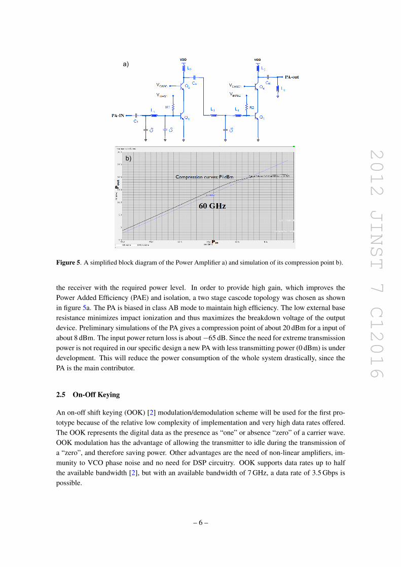
2012 JINST 7 C12016
6 Conclusions and further work
A transceiver using the 60 GHz band as a solution to the bandwidth limitation for a first level tracktrigger and to meet the requirement set by the high data rate in HEP has been proposed Individualblocks under development designed in 130 nm SiGe HBT BiCMOS have been described Firstsimulations show that reasonable noise and power levels at 60 GHz is achieved The choice oftechnology and the benefit of going 3D has been briefly discussed The first prototype of thetransceiver is forseen to be submitted mid 2013
References
[1] R Brenner and S Cheng Multigigabit wireless transfer of trigger data through millimetre wavetechnology 2010 JINST 5 C07002 in Workshop on Intelligent Trackers 2010 Lawrence BerkeleyNational Laboratory Berkeley USA 3ndash5 Feb 2010
[2] J Lee Y Chen and Y Huang A low-power low-cost fully-integrated 60-GHz transceiver system withOOK modulation and on-board antenna assembly IEEE J Solid-St Circ 45 (2010) 264
[3] M Ullan et al Evaluation of two SiGe HBT technologies for the ATLAS sLHC upgrade inProceedings of the Topical Workshop on Electronics for Particle Physics Naxos Greece15ndash19 Sep 2008 pp 111ndash115
[4] GSA Tour guide to 3D-IC design tools amp services DAC 2010httpwwwgsaglobalorgedadocsTour Guide to 3D ToolsServices FINAL 001pdf
ndash 8 ndash