Embed Size (px)
Citation preview

1Zarlink Semiconductor Inc.
Zarlink, ZL and the Zarlink Semiconductor logo are trademarks of Zarlink Semiconductor Inc.Copyright 2003-2006, Zarlink Semiconductor Inc. All Rights Reserved.
Features• 4,096 × 4,096 channel non-blocking switching at
8.192 or 16.384 Mbps
• Per-channel variable or constant throughput delay
• Accepts 32 ST-BUS streams of 2.048 Mbps, 4.096 Mbps, 8.192 Mbps or 16.384 Mbps
• Split Rate mode provides a rate conversion option to convert data from one rate to another rate
• Automatic frame offset delay measurement for ST-BUS input streams
• Per-stream input delay programming
• Per-stream output advancement programming
• Per-channel high impedance output control
• Bit Error Monitoring on selected ST-BUS input and output channels.
• Per-channel message mode
• Connection memory block programming
• IEEE-1149.1 (JTAG) Test Port
• 3.3 V local I/O with 5 V tolerant inputs and TTL compatible outputs
Applications• Medium switching platforms
• CTI application
• Voice/data multiplexer
• Digital cross connects
• WAN access system
• Wireless base stations
January 2006
Ordering InformationMT90826AL 160 Pin MQFP TraysMT90826AG 160 Ball PBGA TraysMT90826AV 144 Ball LBGA TraysMT90826AL1 160 Pin MQFP* TraysMT90826AG2 160 Ball PBGA** Trays
*Pb Free Matte Tin**Pb Free Tin/Silver/Copper
-40°C to +85°C
MT90826 Quad Digital Switch
Data Sheet
Figure 1 - Functional Block Diagram
Test Port
STo0STo1
•••
STo31
STi0/FEi0STi1/FEi1
•••
STi31/FEi31
Parallel
to
Serial
Converter
OutputMUX
Microprocessor InterfaceTiming Unit
InternalRegisters
F0i DS CS R/W A13-A0 DTA D15-D0
ODEVSS
ConnectionMemory
CLK
VDD TDI TDO RESETTCK TRST
Serial
to
Parallel
Converter
TMS
Multiple BufferData Memory
PLLVSSPLLVDD

MT90826 Data Sheet
2Zarlink Semiconductor Inc.
DescriptionThe MT90826 Quad Digital Switch has a non-blocking switch capacity of 4,096 x 4,096 channels at a serial bit rateof 8.192 Mbps or 16.384 Mbps, 2,048 x 2,048 channels at 4.096 Mbps and 1024 x 1024 channels at 2.048 Mbps.The device has many features that are programmable on a per stream or per channel basis, including messagemode, input offset delay and high impedance output control.
The per stream input and output delay control is particularly useful for managing large multi-chip switches with adistributed backplane.
Operating in Split Rate mode allows rate conversion for switching between two groups of bit rate streams.

MT90826 Data Sheet
Table of Contents
3Zarlink Semiconductor Inc.
1.0 Device Overview . . . . . . . . . . . . . . . . . . . . . . . . . . . . . . . . . . . . . . . . . . . . . . . . . . . . . . . . . . . . . . . . . . . . . . 122.0 Functional Description . . . . . . . . . . . . . . . . . . . . . . . . . . . . . . . . . . . . . . . . . . . . . . . . . . . . . . . . . . . . . . . . . 14
2.1 Data and Connection Memory. . . . . . . . . . . . . . . . . . . . . . . . . . . . . . . . . . . . . . . . . . . . . . . . . . . . . . . . . . 142.2 Connection and Message Modes . . . . . . . . . . . . . . . . . . . . . . . . . . . . . . . . . . . . . . . . . . . . . . . . . . . . . . . 142.3 Clock Timing Requirements . . . . . . . . . . . . . . . . . . . . . . . . . . . . . . . . . . . . . . . . . . . . . . . . . . . . . . . . . . . 15
3.0 Switching Configurations . . . . . . . . . . . . . . . . . . . . . . . . . . . . . . . . . . . . . . . . . . . . . . . . . . . . . . . . . . . . . . . 153.1 Serial Input Frame Alignment Evaluation . . . . . . . . . . . . . . . . . . . . . . . . . . . . . . . . . . . . . . . . . . . . . . . . . 163.2 Input Frame Offset Selection. . . . . . . . . . . . . . . . . . . . . . . . . . . . . . . . . . . . . . . . . . . . . . . . . . . . . . . . . . . 163.3 Output Advance Offset Selection . . . . . . . . . . . . . . . . . . . . . . . . . . . . . . . . . . . . . . . . . . . . . . . . . . . . . . . 163.4 Memory Block Programming . . . . . . . . . . . . . . . . . . . . . . . . . . . . . . . . . . . . . . . . . . . . . . . . . . . . . . . . . . . 173.5 Bit Error Rate Monitoring . . . . . . . . . . . . . . . . . . . . . . . . . . . . . . . . . . . . . . . . . . . . . . . . . . . . . . . . . . . . . . 17
4.0 Delay Through the MT90826 . . . . . . . . . . . . . . . . . . . . . . . . . . . . . . . . . . . . . . . . . . . . . . . . . . . . . . . . . . . . . 184.1 Variable Delay Mode (TM1=0, TM0=0) . . . . . . . . . . . . . . . . . . . . . . . . . . . . . . . . . . . . . . . . . . . . . . . . . . . 184.2 Constant Delay Mode (TM1=1, TM0=0) . . . . . . . . . . . . . . . . . . . . . . . . . . . . . . . . . . . . . . . . . . . . . . . . . . 18
5.0 Microprocessor Interface . . . . . . . . . . . . . . . . . . . . . . . . . . . . . . . . . . . . . . . . . . . . . . . . . . . . . . . . . . . . . . . 186.0 Memory Mapping . . . . . . . . . . . . . . . . . . . . . . . . . . . . . . . . . . . . . . . . . . . . . . . . . . . . . . . . . . . . . . . . . . . . . . 297.0 Connection Memory Control. . . . . . . . . . . . . . . . . . . . . . . . . . . . . . . . . . . . . . . . . . . . . . . . . . . . . . . . . . . . . 298.0 DTA Data Transfer Acknowledgment Pin . . . . . . . . . . . . . . . . . . . . . . . . . . . . . . . . . . . . . . . . . . . . . . . . . . 299.0 Initialization of the MT90826 . . . . . . . . . . . . . . . . . . . . . . . . . . . . . . . . . . . . . . . . . . . . . . . . . . . . . . . . . . . . . 3010.0 JTAG Support. . . . . . . . . . . . . . . . . . . . . . . . . . . . . . . . . . . . . . . . . . . . . . . . . . . . . . . . . . . . . . . . . . . . . . . . 30
10.1 Test Access Port (TAP) . . . . . . . . . . . . . . . . . . . . . . . . . . . . . . . . . . . . . . . . . . . . . . . . . . . . . . . . . . . . . . 3010.2 Instruction Register . . . . . . . . . . . . . . . . . . . . . . . . . . . . . . . . . . . . . . . . . . . . . . . . . . . . . . . . . . . . . . . . . 31

MT90826 Data Sheet
List of Figures
4Zarlink Semiconductor Inc.
Figure 1 - Functional Block Diagram . . . . . . . . . . . . . . . . . . . . . . . . . . . . . . . . . . . . . . . . . . . . . . . . . . . . . . . . . . . . 1Figure 2 - 160-Pin MQFP Pin Connections . . . . . . . . . . . . . . . . . . . . . . . . . . . . . . . . . . . . . . . . . . . . . . . . . . . . . . . 7Figure 3 - 160 Ball PBGA Pin Connections . . . . . . . . . . . . . . . . . . . . . . . . . . . . . . . . . . . . . . . . . . . . . . . . . . . . . . . 8Figure 4 - 144 Ball LBGA Pin Connections . . . . . . . . . . . . . . . . . . . . . . . . . . . . . . . . . . . . . . . . . . . . . . . . . . . . . . . 9Figure 5 - Example for Frame Alignment Measurement . . . . . . . . . . . . . . . . . . . . . . . . . . . . . . . . . . . . . . . . . . . . 22Figure 6 - Examples for Input Offset Delay Timing . . . . . . . . . . . . . . . . . . . . . . . . . . . . . . . . . . . . . . . . . . . . . . . . 26Figure 7 - Examples for Frame Output Offset Timing . . . . . . . . . . . . . . . . . . . . . . . . . . . . . . . . . . . . . . . . . . . . . . 28Figure 8 - ST-BUS Timing for Stream rate of 16.384 Mbps . . . . . . . . . . . . . . . . . . . . . . . . . . . . . . . . . . . . . . . . . . 37Figure 9 - ST-BUS Timing for Stream rate of 8.192 Mbps when CLK = 16.384 MHz . . . . . . . . . . . . . . . . . . . . . . 38Figure 10 - ST-BUS Timing for Stream rate of 4.096 Mbps when CLK = 16.384 MHz . . . . . . . . . . . . . . . . . . . . . 38Figure 11 - ST-BUS Timing for Stream rate of 4.096 Mbps when CLK = 8.192 MHz. . . . . . . . . . . . . . . . . . . . . . . 38Figure 12 - ST-BUS Timing for Stream rate of 2.048 Mbps when CLK = 16.384 MHz . . . . . . . . . . . . . . . . . . . . . 39Figure 13 - -BUS Timing for Stream rate of 2.048 Mbps when CLK = 8.192 MHz. . . . . . . . . . . . . . . . . . . . . . . . . 39Figure 14 - Serial Output and External Control . . . . . . . . . . . . . . . . . . . . . . . . . . . . . . . . . . . . . . . . . . . . . . . . . . . 39Figure 15 - Output Driver Enable (ODE) . . . . . . . . . . . . . . . . . . . . . . . . . . . . . . . . . . . . . . . . . . . . . . . . . . . . . . . . 40Figure 16 - Motorola Non-Multiplexed Bus Timing. . . . . . . . . . . . . . . . . . . . . . . . . . . . . . . . . . . . . . . . . . . . . . . . . 42

MT90826 Data Sheet
List of Tables
5Zarlink Semiconductor Inc.
Table 1 - Stream Usage under Various Operation Modes . . . . . . . . . . . . . . . . . . . . . . . . . . . . . . . . . . . . . . . . . . . 13Table 2 - Output High Impedance Control . . . . . . . . . . . . . . . . . . . . . . . . . . . . . . . . . . . . . . . . . . . . . . . . . . . . . . . 13Table 3 - Address Map for Registers (A13 = 0) . . . . . . . . . . . . . . . . . . . . . . . . . . . . . . . . . . . . . . . . . . . . . . . . . . . 13Table 4 - Address Map for Memory Locations (A13 = 1) . . . . . . . . . . . . . . . . . . . . . . . . . . . . . . . . . . . . . . . . . . . . 17Table 5 - Control Register Bits . . . . . . . . . . . . . . . . . . . . . . . . . . . . . . . . . . . . . . . . . . . . . . . . . . . . . . . . . . . . . . . . 19Table 6 - Serial Data Rate Selections and External Clock Rates. . . . . . . . . . . . . . . . . . . . . . . . . . . . . . . . . . . . . . 20Table 7 - Frame Alignment (FAR) Register Bits . . . . . . . . . . . . . . . . . . . . . . . . . . . . . . . . . . . . . . . . . . . . . . . . . . . 21Table 8 - Frame Delay Offset Register (DOS) Bits. . . . . . . . . . . . . . . . . . . . . . . . . . . . . . . . . . . . . . . . . . . . . . . . . 23Table 9 - Frame delay Bits (FD9, FD2-0) and Input Offset Bits (IFn3-0) . . . . . . . . . . . . . . . . . . . . . . . . . . . . . . . . 25Table 10 - Frame Output Offset (FOR) Register Bits . . . . . . . . . . . . . . . . . . . . . . . . . . . . . . . . . . . . . . . . . . . . . . . 27Table 11 - Output Offset Bits (FD9, FD2-0) . . . . . . . . . . . . . . . . . . . . . . . . . . . . . . . . . . . . . . . . . . . . . . . . . . . . . . 27Table 12 - Bit Error Input Selection (BISR) Register Bits . . . . . . . . . . . . . . . . . . . . . . . . . . . . . . . . . . . . . . . . . . . . 28Table 13 - Bit Error Count (BECR) Register Bits . . . . . . . . . . . . . . . . . . . . . . . . . . . . . . . . . . . . . . . . . . . . . . . . . . 28Table 14 - Connection Memory Bits . . . . . . . . . . . . . . . . . . . . . . . . . . . . . . . . . . . . . . . . . . . . . . . . . . . . . . . . . . . . 34Table 15 - SAB and CAB Bits Programming for Various Interface Mode . . . . . . . . . . . . . . . . . . . . . . . . . . . . . . . . 34

MT90826 Data Sheet
6Zarlink Semiconductor Inc.
Changes SummaryThe following table captures the changes from the April 2005 issue.
Page Item Change
26 Figure 6 “Examples for Input Offset Delay Timing”
Clarified the mid-point sampling of the 16 Mbps input data.
30 Section 9.0 Initialization of the MT90826
Added the 600 µs waiting time needed for the APLL module to be stabilized before starting the next microprocessor port access cycle.
37 AC Electrical Characteristics - Serial Streams for ST-BUS.
Clarified the 16, 8, 4 and 2 Mbps Input Data Sampling timing.
37 Figure 8 “ST-BUS Timing for Stream rate of 16.384 Mbps”
Clarified the input data sampling position at 16 Mbps data rate.
38 Figure 9 “ST-BUS Timing for Stream rate of 8.192 Mbps when CLK = 16.384 MHz”
Added the input data sampling position at 8 Mbps data rate.
38 Figure 10 “ST-BUS Timing for Stream rate of 4.096 Mbps when CLK = 16.384 MHz”
Added the input data sampling position at 4 Mbps data rate.
39 Figure 12 “ST-BUS Timing for Stream rate of 2.048 Mbps when CLK = 16.384 MHz”
Added the input data sampling position at 2 Mbps data rate.

MT90826 Data Sheet
7Zarlink Semiconductor Inc.
Figure 2 - 160-Pin MQFP Pin Connections
STo
16S
To17
STo
18S
To19
STo
20S
To21
STo22STo23
ODE
STo24STo25STo26
STi0/FEi0STi1/FEi1STi2/FEi2STi3/FEi3
STi4/FEi4STi5/FEi5STi6/FEi6STi7/FEi7
STi8/FEi8STi9/FEi9
STi
10/F
Ei1
0
STi
12/F
Ei1
2
A3
TCK
TDOA8
A9
A10
A11
A12
A13A2
STo27
STo28STo29STo30STo31
STi
11/F
Ei1
1
STi
15/F
Ei1
5S
Ti14
/FE
i14
STi
13/F
Ei1
3
TDI
D1
D3D4D5D6D7
D9
D10
D11
D12
D13
DTA
TRS
T
D2
D0
IC1
TMS
160 Pin MQFP
RESET
103109111113 959799101117 91115 93 89107 105119
135
141
143
145
127
129
131
133
149
123
147
125
121
139
137
151
57
55
53
51
49
65
67
63
61
59
47
45
43
69
71
41
171513119 25 27232119753 29 311
STi
16/F
Ei1
6S
Ti17
/FE
i17
STi
18/F
Ei1
8S
Ti19
/FE
i19
STi
20/F
Ei2
0
VS
S
STi
21/F
Ei2
1S
Ti22
/FE
i22
STi
23/F
Ei2
3
STi24/FEi24STi25/FEi25STI26/FEi26STi27/FEi27
STi28/FEi28STi29/FEi29
STi31/FEi31
VSS
VDD
CLK
VSS
STo
13S
To12
STo7STo6STo5STo4
STo3
VDD
VS
S
D8
A4
IC2
STo
8
STo
15S
To14
STo
9
87 8385 81
STo
10
33 35 37 39
CS
R/W DS A0
A1
153
157
155
159
STo
11
D14
D15
73
75
77
79
F0i
PLLGNDNC
IC3
VDDVSS
VDD
VS
S
VSS
NC
NC
PLLVDD
VDD
VDDVSS
VS
S
VS
S
VS
S
VS
SVD
D
VSSVDD
VSS
VSSVDD
VSSVDD
VDD
VS
S
VDD
VS
S
STi30/FEi30 STo2
VSS
STo0STo1
NC
NC
VSS
VDD
NC
VSS
NC
NC
NC
A7
A6
A5
NC
VS
S
NC
NC
NC
28 mm x 28 mmPin Pitch 0.65 mm

MT90826 Data Sheet
8Zarlink Semiconductor Inc.
Figure 3 - 160 Ball PBGA Pin Connections
B
C
D
E
F
G
H
J
K
L
M
N
1 2 3 4 5 6 7 8 9 10 11 12 131
1 - A1 corner is identified by metallized markings.
A
STo22STo24STo27
STi29 NCSTi31
STo30 STo31 D2
D4
D5 D6
D10
D13
D11
D14
D12
NC
D15
NC
R/W
NC
A1DS A2 A4 A5 A6 TMS
A12 A13
TDO TCK
IC1
RESET
IC2 IC3
CLKF0i
ODENC
NC STi0STi1
STi2
STi6STi7
STo4
STo2
STo5
STo6STo3
STo7STi12STi15STo16
NC A9
PLLGND
STi13
D7
A10
PLLVDD
STo0
STi14
D0
VDDVDDVDDVDDVDDGND GND
NCNCVDDVDDVDDGND
NC
GND
VDD
VDD
VDD
VDD
VDD
VDD
VDD
VDD
VDD
GND
GND
GND
GND
GND
STi26 STi24 STo20 STi22 STi20 STi18 STi16 STo15 STo13 STo10 STo8 STi10 STi9
STi27 STi25 STo21 STi23 STi21 STi19 STi17 STo14 STo12 STo11 STo9 STi11 STi8
STo26 STo25 STo23 STo19 STo18 STo17
GNDGNDGNDGND
GND
GND GNDGNDGNDGND
GND
STi28 NCSTi30
STi3
STo1 STi4STi5
STo28 STo29
D1 D3
D9D8
DTA CS A0 A3 A8A7 A11 TDI TRST
23mm x 23mm
TOP VIEW
Ball Pitch 1.5mm

MT90826 Data Sheet
9Zarlink Semiconductor Inc.
Figure 4 - 144 Ball LBGA Pin Connections
PINOUT DIAGRAM: (as viewed through top of package)
A1 corner identified by metallized marking, mould indent, ink dot or right-angled corner
1 2 3 4 5 6 7 8 9 10 11 12
A STo23 STo20 STi21 STi20 STi17 STi16 STo14 STo13 STo11 STo9 STi11 STi9
B STo22 STo21 STi23 STi22 STi19 STi18 STo15 STo12 STo10 STo8 STI10 STi8
C STi26 STi25 STo24 STo19 STo18 STo17 STo16 STi14 STi13 STi12 STo7 STo5
D STi27 STi24 STo25 GND VDD VDD VDD STi15 GND STo2 STo6 STo4
E STi29 STi28 STo27 STo26 GND GND GND GND VDD STo3 STi7 STi6
F STi30 STi31 STo28 VDD GND GND GND GND VDD STo1 STi4 STi5
G STo30 STo31 STo29 VDD GND GND GND GND PLLVDD STo0 STi3 STi2
H D1 D2 D0 VDD GND GND GND GND PLLGND ODE STi0 STi1
J D3 D7 D4 GND DS VDD VDD VDD NC NC FOi CLK
K D5 D15 D11 D13 CS A2 A5 A8 A9 RESET IC1 IC3
L D6 D8 D9 R/W A13 A1 A4 A10 A12 TCK TDO IC2
M D10 D12 D14 DTA A0 A3 A6 A7 A11 TMS TDI TRST

MT90826 Data Sheet
10Zarlink Semiconductor Inc.
Pin Description
Pin # MQFP Pin # PBGA Pin # LBGA Name Description
12,22,33,54,66,77,90,101,112,125,136,
147,157
D5,D6,D7,D8,D9,E4,E10,F4,
F10,G4,G10,H4,J4,J10,K5,
K6,K7
D5,D6,D7,E9,F4,F9,G4,H4,
J6,J7,J8
VDD +3.3 Volt Power Supply.
11,21,32,45,53,60,65,71,76,84,89,95,100,106,111,117,124,130,135,141,146,
156
D4,D10,E5,E6,E7,E8,E9,F5,F9,G5,G9,H5,H9,H10,J5,J6,
J7,J8,J9,K4
D4,D9,E5,E6,E7,E8,F5,F6,F7,F8,G5,G6,G7,G8,H5,H6,
H7,H8,J4
Vss Ground.
34 N11 M10 TMS Test Mode Select (3.3 V Input with Internal pull-up). JTAG signal that controls the state transitions of the TAP controller. This pin is pulled high by an internal pull-up when not driven.
35 M11 M11 TDI Test Serial Data In (3.3 V Input with Internal pull-up). JTAG serial test instructions and data are shifted in on this pin. This pin is pulled high by an internal pull-up when not driven.
36 N12 L11 TDO Test Serial Data Out (3.3 V Output). JTAG serial data is output on this pin on the falling edge of TCK. This pin is held in high impedance state when JTAG scan is not enabled.
37 N13 L10 TCK Test Clock (5 V Tolerant Input). Provides the clock to the JTAG test logic.
38 M12 M12 TRST Test Reset (3.3 V Input with internal pull-up). Asynchronously initializes the JTAG TAP controller by putting it in the Test-Logic-Reset state. This pin is pulled by an internal pull-up when not driven. This pin should be pulsed low on power-up, or held low, to ensure that the device is in the normal functional mode.
42 L11 K11 IC1 Internal Connection 1 (3.3 V Input with internal pull-down). Connect to VSS for normal operation.
43 M13 K10 RESET Device Reset (5 V Tolerant Input). This input (active LOW) puts the device in its reset state which clears the device internal counters and registers.

MT90826 Data Sheet
11Zarlink Semiconductor Inc.
44 L12 L12 IC2 Internal Connection 2 (3.3 V Input with internal pull-down). Connect to VSS for normal operation.
46 L13 K12 IC3 Internal Connection 3 (3.3 V Input with internal pull-down). Connect to VSS for normal operation.
47 K12 J11 F0i Master Frame Pulse (5 V Tolerant Input). This input accepts a 122 ns or 60 ns wide negative frame pulse. The CPLL bit in the control register determines the usage of the frame pulse width. See Table 6 for details.
50 K10 H9 PLLGND Phase Lock Loop Ground.
51 K9 G9 PLLVDD Phase Lock Loop Power Supply. 3.3 V
52 K13 J12 CLK Master Clock (5 V Tolerant Input). Serial clock for shifting data in/out on the serial streams. This pin accepts a clock frequency of 8.192 MHz or 16.384 MHz. The CPLL bit in the control register determines the usage of the clock frequency. See Table 6 for details.
55 J13 H10 ODE Output Drive Enable (5 V Tolerant Input). This is the output-enable control pin for the STo0 to STo31 serial outputs. See Table 2 for details.
56575859
67-7078,7982,8391-94
102-105113-116126-129137-140
H13H12G13G12
F13,F12,E13,E12B13,A13A12,B12
C11,C10,C9,C8A7,B7,A6,B6A5,B5,A4,B4A2,B2,A1,B1E2,F2,E1,F1
H11H12G12G11
F11,F12,E12,E11B12,A12B11,A11
C10,C9,C8,D8A6,A5,B6,B5,A4,A3,B4,B3D2,C2,C1,D1E2,E1,F1,F2
STi0/FEi0,STi1/FEi1STi2/FEi2STi3/FEi3
STi4-7/FEi4-7STi8-9/FEi8-9
STi10-11/FEi10-11STi12-15/FEi12-15STi16-19/FEi16-19STi20-23/FEi20-23STi24-27/FEi24-27STi28-31/FEi28-31
Serial Input Streams 0 to 31 and Frame Evaluation Inputs 0 to 31 (5 V Tolerant Inputs). Serial data input streams. These streams may have data rates of 2.048, 4.096, 8.192 or 16.384 Mbps, depending upon the value programmed at bits DR0 - DR2 in the control register. In the frame evaluation mode, they are used as the frame evaluation inputs.
61-6472-7585-8896-99
107-110118,119122,123131-134142-145
G11,F11,E11,D11D13,C13,D12,C12A11,B11,A10,B10
B9,A9,B8,A8C7,C6,C5,C4
A3,B3D3,C3
D2,C2,C1,D1G1,G2,H1,H2
G10,F10,D10,E10D12,C12,D11,C11
B10,A10,B9,A9B8,A8,A7,B7C7,C6,C5,C4
A2,B2B1,A1
C3,D3,E4,E3F3,G3,G1,G2
STo0 - 3STo4 - 7STo8 - 11
STo12 - 15STo16 - 19
STo20, STo21STo22, STo23
STo24 - 27STo28 - 31
ST-BUS Output 0 to 31 (Three-state Outputs). Serial data output streams. These streams may have data rates of 2.048, 4.096, 8.192, or 16.384 Mbps, depending upon the value programmed at bits DR0 - DR2 in the control register.
Pin Description (continued)
Pin # MQFP Pin # PBGA Pin # LBGA Name Description

MT90826 Data Sheet
12Zarlink Semiconductor Inc.
1.0 Device OverviewThe MT90826 Quad Digital Switch is capable of switching up to 4,096 × 4,096 channels. The MT90826 is designedto switch 64 Kbps PCM or N x 64 Kbps data. The device maintains frame integrity in data applications and minimumthroughput delay for voice applications on a per channel basis.
The serial input streams of the MT90826 can have a bit rate of 2.048, 4.096, 8.192 or 16.384 Mbps and arearranged in 125 µs wide frames, which contain 32, 64,128 or 256 channels, respectively. The data rates on inputand output streams match. All inputs and outputs may be programmed to 2.048, 4.096 or 8.192 Mbps. STi0-15 andSTo0-15 may be set to 16.384 Mbps. Combinations of two bit rates, N and 2N are provided. See Table 1.
By using Zarlink’s message mode capability, the microprocessor can access input and output timeslots on a perchannel basis. This feature is useful for transferring control and status information for external circuits or other ST-BUS devices.
To correct for backplane delays, the MT90826 has a frame offset calibration function which allows users to measurethe frame delay on any of the input streams, This information can then be used to program the input offset dealy foreach individual stream. Refer to Table 7, 8, and 9 and Figure 6. In addition, the MT90826 allow users to advance
148 - 153154,155
1583 - 78,9
G3,J1,H3,J2,J3,K1,K2,K3
L1L2,M1,M2,M3,N1,
N2,N3
H3,H1,H2,J1,J3,K1L1,J2
L2L3,M1,K3,M2,K4
M3,K2
D0 - 5,D6, D7
D8D9 - 13
D14, D15
Data Bus 0 to 15 (5 V Tolerant I/O). These pins form the 16-bit data bus of the microprocessor port.
10 M4 M4 DTA Data Transfer Acknowledgment (Three-state Output). This output pulses low from tristate to indicate that a databus transfer is complete. A pull-up resistor is required to hold a HIGH level when the pin is tristated.
15 N5 J5 DS Data Strobe (5 V Tolerant Input). This active low input works in conjunction with CS to enable the read and write operations.
14 N4 L4 R/W Read/Write (5 V Tolerant Input). This input controls the direction of the data bus lines (D0-D15) during a microprocessor access.
13 M5 K5 CS Chip Select (5 V Tolerant Input). Active low input used by a microprocessor to activate the microprocessor port.
16 - 2023 - 31
M6,N6,N7,M7,N8N9,N10,M8,M9,L7
L8,M10,L9,L10
M5,L6,K6,M6,L7,K7,M7,M8,K8,K9,
L8,M9,L9,L5
A0 - A4A5 - A13
Address 0 to 13 (5 V Tolerant Input). These lines provide the A0 - A13 address lines when accessing the internal registers or memories.
1,2,39,40,41,48,49,80,81,120,121,159,160
E3,F3,H11,J11,J12,K8,K11,L3,L4,L5,L6.
J9,J10 NC No Connect. These pins have to be left unconnected.
Pin Description (continued)
Pin # MQFP Pin # PBGA Pin # LBGA Name Description

MT90826 Data Sheet
13Zarlink Semiconductor Inc.
the output data position up to 45ns to compensate for the output delay caused by excessive output loadingconditions. See Figure 7 “Examples for Frame Output Offset Timing”.
The microport interface is compatible with Motorola non-multiplexed buses. Connection memory locations may bedirectly written to or read from; data memory locations may be directly read from. A DTA signal is provided to holdthe bus until the asynchronous microport operation is queued into the device.
Serial Interface Mode Input Stream Input Data Rate Output Stream Output Data Rate
8 Mbps STi0-31 8 Mbps STo0-31 8 Mbps
16 Mbps STi0-15 16 Mbps STo0-15 16 Mbps
4 Mbps and 8 Mbps STi0-15 4 Mbps STo0-15 4 Mbps
STi15-31 8 Mbps STo16-31 8 Mbps
16 Mbps and 8 Mbps STi0-11 16 Mbps STo0-11 16 Mbps
STi12-19 8 Mbps STo12-19 8 Mbps
4 Mbps STi0-31 4 Mbps STo0-31 4 Mbps
2 Mbps and 4 Mbps STi0-15 2 Mbps STo0-15 2 Mbps
STi16-31 4 Mbps STo16-31 4 Mbps
2 Mbps STi0-31 2 Mbps STo0-31 2 Mbps
Table 1 - Stream Usage under Various Operation Modes
ODE pin OSB bit in Control register OE bit in Connection Memory ST-BUS Output Driver
0 0 X High-Z
X X 0 Per Channel High-Z
1 0 1 Enable
0 1 1 Enable
1 1 1 Enable
Table 2 - Output High Impedance Control
A13 A12 A11 A10 A9 A8 A7 A6 A5 A4 A3 A2 A1 A0 Location
0 0 0 0 0 0 0 0 0 0 0 0 0 0 Control Register, CR
0 0 0 0 0 0 0 0 0 0 0 0 0 1 Frame Alignment Register, FAR
0 0 0 0 0 0 0 0 0 0 0 0 1 0 Input Offset Selection Register 0, DOS0
0 0 0 0 0 0 0 0 0 0 0 0 1 1 Input Offset Selection Register 1, DOS1
0 0 0 0 0 0 0 0 0 0 0 1 0 0 Input Offset Selection Register 2, DOS2
0 0 0 0 0 0 0 0 0 0 0 1 0 1 Input Offset Selection Register 3, DOS3
0 0 0 0 0 0 0 0 0 0 0 1 1 0 Input Offset Selection Register 4, DOS4
Table 3 - Address Map for Registers (A13 = 0)

MT90826 Data Sheet
14Zarlink Semiconductor Inc.
2.0 Functional DescriptionA functional Block Diagram of the MT90826 is shown in Figure 1.
2.1 Data and Connection Memory
For all data rates, the received serial data is converted to parallel format by internal serial-to-parallel converters andstored sequentially in the data memory. Depending upon the selected operation programmed in the control register,the usable data memory may be as large as 4,096 bytes. The sequential addressing of the data memory isperformed by an internal counter, which is reset by the input 8 kHz frame pulse (F0i) to mark the frame boundariesof the incoming serial data streams.
Data to be output on the serial streams may come from either the data memory or connection memory. Locations inthe connection memory are associated with particular ST-BUS output channels. When a channel is due to betransmitted on an ST-BUS output, the data for this channel can be switched either from an ST-BUS input inconnection mode, or from the lower half of the connection memory in message mode. Data destined for a particularchannel on a serial output stream is read from the data memory or connection memory during the previous channeltimeslot. This allows enough time for memory access and parallel-to-serial conversion.
2.2 Connection and Message Modes
In the connection mode, the addresses of the input source data for all output channels are stored in the connectionmemory. The connection memory is mapped in such a way that each location corresponds to an output channel onthe output streams. For details on the use of the source address data (CAB and SAB bits), see Table 14. Once thesource address bits are programmed by the microprocessor, the contents of the data memory at the selectedaddress are transferred to the parallel-to-serial converters and then onto an ST-BUS output stream.
By having several output channels connected to the same input source channel, data can be broadcast from oneinput channel to several output channels.
In message mode, the microprocessor writes data to the connection memory locations corresponding to the outputstream and channel number. The lower half (8 least significant bits) of the connection memory content is
0 0 0 0 0 0 0 0 0 0 0 1 1 1 Input Offset Selection Register 5, DOS5
0 0 0 0 0 0 0 0 0 0 1 0 0 0 Input Offset Selection Register 6, DOS6
0 0 0 0 0 0 0 0 0 0 1 0 0 1 Input Offset Selection Register 7, DOS7
0 0 0 0 0 0 0 0 0 0 1 0 1 0 Frame Output Offset Register, FOR0
0 0 0 0 0 0 0 0 0 0 1 0 1 1 Frame Output Offset Register, FOR1
0 0 0 0 0 0 0 0 0 0 1 1 0 0 Frame Output Offset Register, FOR2
0 0 0 0 0 0 0 0 0 0 1 1 0 1 Frame Output Offset Register, FOR3
0 0 0 0 0 0 0 0 0 0 1 1 1 0 Unused
0 0 0 0 0 0 0 0 0 0 1 1 1 1 Unused
0 0 0 0 0 0 0 0 0 1 0 0 0 0 Unused
0 0 0 0 0 0 0 0 0 1 0 0 0 1 Bit Error Input Selection Register, BISR
0 0 0 0 0 0 0 0 0 1 0 0 1 0 Bit Error Count Register, BECR
A13 A12 A11 A10 A9 A8 A7 A6 A5 A4 A3 A2 A1 A0 Location
Table 3 - Address Map for Registers (A13 = 0) (continued)
MT90826 Data Sheet
15Zarlink Semiconductor Inc.
transferred directly to the parallel-to-serial converter. This data will be output on the ST-BUS streams in every frameuntil the data is changed by the microprocessor.
The three most significant bits of the connection memory controls the following for an output channel: message orconnection mode, constant or variable delay mode, enables/tristate the ST-BUS output drivers and bit error testpattern enable. If an output channel is set to a high-impedance state by setting the OE bit to zero in the connectionmemory, the ST-BUS output will be in a high impedance state for the duration of that channel. In addition to the per-channel control, all channels on the ST-BUS outputs can be placed in a high impedance state by pulling the ODEinput pin low and programming the output stand by (OSB) bit in the control register to low. This action overrides theindividual per-channel programming by the connection memory bits. See Table 2 for detail.
The connection memory data can be accessed via the microprocessor interface through the D0 to D15 pins. Theaddressing of the device internal registers, data and connection memories is performed through the address inputpins and the Memory Select (MS) bit of the control register.
2.3 Clock Timing Requirements
The master clock (CLK) frequency must be either at 8.192 MHz or 16.384 MHz for serial data rate of 2.048, 4.096,8.192 and 16.384 Mbps; see Table 6 for the selections of the master clock frequency.
3.0 Switching ConfigurationsThe MT90826 maximum non-blocking switching configurations is determined by the data rates selected for theserial inputs and outputs. The switching configuration is selected by three DR bits in the control register. See Table5 and Table 6.
8 Mbps mode (DR2=0, DR1=0, DR0=0)
When the 8 Mbps mode is selected, the device is configured with 32-input/32-output data streams each having 12864 Kbps channels. This mode allows a maximum non-blocking capacity of 4,096 x 4,096 channels. Table 1summarizes the switching configurations and the relationship between different serial data rates and the masterclock frequencies.
16 Mbps mode (DR2=0, DR1=0, DR0 =1)
When the 16 Mbps mode is selected, the device is configured with 16-input/16-output data streams each having256 64 Kbps channels. This mode allows a maximum non-blocking capacity of 4,096 x 4,096 channels.
4 Mbps and 8 Mbps mode (DR2=0, DR1=1, DR0=0)
When the 4 Mbps and 8 Mbps mode is selected, the device is configured with 32-input/32-output data streams.STi0-15/STo0-15 have a data rate of 4 Mbps and STi16-31/STo16-31 have a data rate of 8 Mbps. This mode allowsa maximum non-blocking capacity of 3,072 x 3,072 channels. The MT90826 is capable of rate conversion, allowing4 Mbps input to be converted to 8 Mbps output and vice versa.
16 Mbps and 8 Mbps mode (DR2=0, DR1=1, DR0=1)
When the 16 Mbps and 8 Mbps mode is selected, the device is configured with 20-input/20-output data streams.STi0-11/STo0-11 have a data rate of 16 Mbps and STi12-19/STo12-19 have a data rate of 8 Mbps. This modeallows a maximum non-blocking capacity of 4,096 x 4,096 channels. The MT90826 is capable of rate conversion,allowing 16 Mbps input to be converted to 8 Mbps output and vice versa.
4 Mbps mode (DR2=1, DR1=0, DR0=0)
When the 4 Mbps mode is selected, the device is configured with 32-input/32-output data streams each having 6464 Kbps channels. This mode allows a maximum non-blocking capacity of 2,048 x 2,048 channels.

MT90826 Data Sheet
16Zarlink Semiconductor Inc.
2 Mbps and 4 Mbps mode (DR2=1, DR1=0, DR0=1)
When the 2 Mbps and 4 Mbps mode is selected, the device is configured with 32-input/32-output data streams.STi0-15/STo0-15 have a data rate of 2 Mbps and STi16-31/STo16-31 have a data rate of 4 Mbps. This modeallows a maximum non-blocking capacity of 1,536 x 1,536 channels. The MT90826 is capable of rate conversion,allowing 2 Mbps input to be converted to 4 Mbps output and vice versa.
2 Mbps mode (DR2=1, DR1=1, DR0 =0)
When the 2 Mbps mode is selected, the device is configured with 32-input/32-output data streams each having 3264 Kbps channels. This mode allows a maximum non-blocking capacity of 1,024 x 1,024 channels.
3.1 Serial Input Frame Alignment Evaluation
The MT90826 provides the frame evaluation inputs, FEi0 to FEi31, to determine different data input delays withrespect to the frame pulse F0i. By using the frame evaluation input select bits (FE0 to FE4) of the frame alignmentregister (FAR), users can select one of the thirty-two frame evaluation inputs for the frame alignment measurement.
The internal master clock, which has a fixed relationship with the CLK and F0i depending upon the mode ofoperation, is used as the reference timing signal to determine the input frame delays. See Figure 5 for the signalalignments between the internal and the external master clocks.
A measurement cycle is started by setting the start frame evaluation (SFE) bit low for at least one frame. Then theevaluation starts when the SFE bit in the control register is changed from low to high. Two frames later, thecomplete frame evaluation (CFE) bit of the frame alignment register changes from low to high to signal that a validoffset measurement is ready to be read from bits 0 to 9 of the FAR register. The SFE bit must be set to zero beforea new measurement cycle started.
The falling edge of the frame measurement signal (FEi) is evaluated against the falling edge of the frame pulse(F0i). See Table 7 for the description of the frame alignment register.
3.2 Input Frame Offset Selection
Input frame offset selection allows the channel alignment of individual input streams, which operate at 4.096 Mbps,8.192 Mbps or 16.384 Mbps, to be shifted against the input frame pulse (F0i). The input offset selection is notavailable for streams operated at 2.048 Mbps. This feature is useful in compensating for variable path delayscaused by serial backplanes of variable lengths, which may be implemented in large centralized and distributedswitching systems.
Each input stream has its own delay offset value programmed by the input delay offset registers. Each delay offsetregister can control 4 input streams. There are eight delay offset registers (DOS0 to DOS7) to control 32 inputstreams. Possible adjustment can range up to +4.5 internal master clock periods forward with resolution of 0.5internal master clock period. See Table 8 and Table 9 for frame input delay offset programming.
3.3 Output Advance Offset Selection
The MT90826 allows users to advance individual output streams up to 45 ns with a resolution of 15 ns when thedevice is in 8 Mbps, 16 Mbps, 4 and 8 Mbps or 16 and 8 Mbps mode. The output delay adjustment is useful incompensating for variable output delays caused by various output loading conditions. The frame output offsetregisters (FOR0 & FOR3) control the output offset delays for each output streams via the programming of the OFnbits.
See Table 10 and Table 11 for the frame output offset programming.

MT90826 Data Sheet
17Zarlink Semiconductor Inc.
3.4 Memory Block Programming
The MT90826 provides users with the capability of initializing the entire connection memory block in two frames.Bits 13 to 15 of every connection memory location will be programmed with the pattern stored in bits 13 to 15 of thecontrol register.
The block programming mode is enabled by setting the memory block program (MBP) bit of the control registerhigh. When the block programming enable (BPE) bit of the control register is set to high, the block programmingdata will be loaded into the bits 13 to 15 of every connection memory location. The other connection memory bits(bit 0 to 12) are loaded with zeros. When the memory block programming is complete, the device resets the BPE bitto zero.
3.5 Bit Error Rate Monitoring
The MT90826 allows users to perform bit error rate monitoring by sending a pseudo random pattern to a selectedST-BUS output channel and receiving the pattern from a selected ST-BUS input channel. The pseudo randompattern is internally generated by the device with the polynomial of 215 -1.
Users can select the pseudo random pattern to be presented on a ST-BUS channel by programming the TM0 andTM1 bits in the connection memory. When TM0 and TM1 bits are high, the pseudo random pattern is output to theselected ST-BUS output channel. The pseudo random pattern is then received by a ST-BUS input channel which isselected using the BSA and BCA bits in the bit error rate input selection register (BISR). An internal bit error counterkeeps track of the error counts which is then stored in the bit error count register (BECR).
The bit error test is enabled and disabled by the SBER bit in the control register. Setting the bit from zero to oneinitiates the bit error test and enables the internal bit error counter. When the bit is programmed from one to zero,
A13
Stream Address (ST0-31) Channel Address (Ch0-255)
A12 A11 A10 A9 A8 StreamLocation A7 A6 A5 A4 A3 A2 A1 A0 Channel
Location
111111111...1111111111
000000000...1111111111
000000001...0011111111
000011110...1100001111
001100110...1100110011
010101010...0101010101
Stream 0Stream 1Stream 2Stream 3Stream 4Stream 5Stream 6Stream 7Stream 8...Stream 22Stream 23Stream 24Stream 25Stream 26Stream 27Stream 28Stream 29Stream 30Stream 31
00..0000..0000.0011.11
00..0000..0011.1100.11
00..0011..1100.1100.11
00..1100..1100.1100.11
00..1100..1100.1100.11
00..1100..1100.1100.11
00..1100..1100.1100.11
01..0101..0101.0101.01
Ch 0Ch 1..Ch 30Ch 31 (Note 2)Ch 32Ch 33..Ch 62Ch 63 (Note 3)Ch 64Ch 65.Ch 126Ch 127 (Note 4)Ch 128Ch 129.Ch 254Ch 255 (Note 5)
1. Bit A13 must be high for access to data and connection memory positions. Bit A13 must be low for access to registers.2. Channels 0 to 31 are used when serial stream is at 2Mbps.3. Channels 0 to 63 are used when serial stream is at 4Mbps4. Channels 0 to 127 are used when serial stream is at 8Mbps5. Channels 0 to 255 are used when serial stream is at 16Mbps
Table 4 - Address Map for Memory Locations (A13 = 1)

MT90826 Data Sheet
18Zarlink Semiconductor Inc.
the device stops the bit error rate test and the internal bit error counter and transfers the error counts to the bit errorcount register.
In the control register, a zero to one transition of the CBER bit resets the bit error count register and the internal biterror counter.
The MT90826 does not recognize an input of all 1s as an error. If all 1s are being fed into the input stream andchannel, the BERT on chip BECR does not increment. This test is performed by sending defined data through themessage mode to ensure there is proper connectivity, and then running the BER test normally.
4.0 Delay Through the MT90826The switching of information from the input serial streams to the output serial streams results in a throughput delay.The device can be programmed to perform timeslot interchange functions with different throughput delaycapabilities on the per-channel basis. For voice application, select variable throughput delay to ensure minimumdelay between input and output data. In wideband data applications, select constant throughput delay to maintainthe frame integrity of the information through the switch.
The delay through the device varies according to the type of throughput delay selected by the TM bits in theconnection memory.
4.1 Variable Delay Mode (TM1=0, TM0=0)
The delay in this mode is dependent only on the combination of source and destination channels and isindependent of input and output streams. The delay through the switch can vary from 3 channels to 1 frame + 3channels. The Variable delay is only available for odd number output streams but not for the even number outputstreams. Avoid programming the TM0 and TM1 bits to zero in the connection memory when the destination outputstreams are STo0, 2, 4, ..., 28 and 30.
4.2 Constant Delay Mode (TM1=1, TM0=0)
In this mode, frame integrity is maintained in all switching configurations by making use of a multiple data memorybuffer. The delay through the switch is always two frames. The constant delay mode is available for all outputstreams.
5.0 Microprocessor InterfaceThe MT90826 provides a parallel microprocessor interface for non-multiplexed bus structures. This interface iscompatible with Motorola non-multiplexed buses. The required microprocessor signals are the 16-bit data bus (D0-D15), 14-bit address bus (A0-A13) and 4 control lines (CS, DS, R/W and DTA). See Figure 16 for Motorola non-multiplexed microport timing.
The MT90826 microport provides access to the internal registers, connection and data memories. All locationsprovide read/write access except for the data memory and BECR registers which are read only.
For data memory read operations, two consecutive microprocessor cycles are required. The read address (A0-A13)should remain the same for the two consecutive read cycles. The data memory content from the first read cycleshould be ignored.

MT90826 Data Sheet
19Zarlink Semiconductor Inc.
Bit Name Description
15 - 13 BPD2-0 Block Programming Data. These bits carry the value to be loaded into the connection memory block whenever the memory block programming feature is activated. After the MBP bit is set to 1 and the BPE bit is set to 1, the contents of the bits BPD2- 0 are loaded into bit 15 to bit 13 of the connection memory. Bit 12 to bit 0 of the connection memory are set to 0.
12 Unused Must be zero for normal operation.
11 CPLL PLL Input Frequency Select. When zero or one, the CLK input is 16.384 MHz and the F0i input is 60 ns wide. When one, the CLK input is 8.192 MHz and the F0i input is 122 ns wide. See Table 6 for the usage of the clock frequency.
10 CBER Clear Bit Error Rate Register. A zero to one transition in this bit resets the internal bit error counter and the bit error count register to zero.
9 SBER Start Bit Error Rate Test. A zero to one transition in this bit starts the bit error rate test. The bit error test result is kept in the bit error count register. A one to zero transition stops the bit error rate test and the internal bit error counter.
8 SFE Start Frame Evaluation. A zero to one transition in this bit starts the frame evaluation procedure. When the CFE bit in the frame alignement (FAR) register changes from zero to one, the evaluation procedure stops. To start another frame evaluation cycle, set this bit to zero.
7 Unused Must be zero for normal operation.
6 BPE Begin Block programming Enable. A zero to one transition of this bit enables the memory block programming function. The BPE and BPD2-0 bits have to be defined in the same write operation. Once the BPE bit is set high, the device requires two frames to complete the block programming. After the programming function has finished, the BPE bit returns to zero to indicate the operation is completed. When the BPE = 1, the BPE or MBP can be set to 0 to abort the programming operation.When BPE = 1, the other bits in the control register must not be changed for two frames to ensure proper operation.
5 MBP Memory Block Program. When 1, the connection memory block programming feature is ready to program Bit13 to Bit15 of the connection memory. When 0, feature is disabled.
Table 5 - Control Register Bits
Read/Write Address: 0000H,Reset Value: 0000H.
7 6 5 4 3 2 1 08910111213
DR0DR1BPE
1415
SFE 0 OSBMBP MSSBERBPD2 BPD1 BPD0 CBER0 DR2CPLL

MT90826 Data Sheet
20Zarlink Semiconductor Inc.
4 MS Memory Select. When 0, connection memory is selected for read or write operations. When 1, the data memory is selected for read operations and connection memory is selected for write operations. (No microprocessor write operation is allowed for the data memory.)
For data memory read operations, two consecutive microprocessor cycles are required. The read address should remain the same for the two consecutive read cycles. The data memory content from the first read cycle should be ignored. The correct data memory content will be presented to the data bus on the second read cycle.
3 OSB Output Stand By. This bit controls the device output drivers. OSB bit ODE pin OE bit STo0 - 31 0 1 1 Enable 1 0 1 Enable 1 1 1 Enable 0 0 X High impedance state X X 0 Per-channel high impedance
2 - 0 DR2-0 Data Rate Select. Input/Output data rate selection. See next table (Table 6) for detailed programming.
DR2 DR1 DR0 Serial Interface ModeCLK
(CPLL=0)CLK
(CPLL=1)
0 0 0 8 Mbps
16.384 MHz 16.384 MHz
0 0 1 16 Mbps
0 1 0 4 and 8 Mbps
0 1 1 16 and 8 Mbps
1 0 0 4 Mbps 16.384 MHz 8.192 MHz
1 0 1 2 and 4 Mbps
1 1 0 2 Mbps 16.384 MHz 8.192 MHz
Table 6 - Serial Data Rate Selections and External Clock Rates
Bit Name Description
Table 5 - Control Register Bits (continued)
Read/Write Address: 0000H,Reset Value: 0000H.
7 6 5 4 3 2 1 08910111213
DR0DR1BPE
1415
SFE 0 OSBMBP MSSBERBPD2 BPD1 BPD0 CBER0 DR2CPLL

MT90826 Data Sheet
21Zarlink Semiconductor Inc.
Bit Name Description
15 - 11 FE4-0 Frame Evaluation Input Select. The binary value expressed in these bits refers to the frame evaluation inputs, FEi0 to FEi31.
10 CFE Complete Frame Evaluation. When CFE = 1, the frame evaluation is completed and FD9 to FD0 bits contains a valid frame alignment offset.This bit is reset to zero, when SFE bit in the control register is changed from 1 to 0.
9 FD9 Frame Delay Bit 9. The falling edge of FEi input is sampled during the internal master clock high phase (FD9 = 1) or during the low phase (FD9 = 0). This bit allows the measurement resolution to 1/2 internal master clock cycle.See Figure 5 for clock signal alignment.
Internal Master Clock Operation Mode C8i 2 Mbps C16i 4 Mbps, 2&4 Mbps C32i 8 Mbps, 16 Mbps, 4&8 Mbps, 16&8 Mbps
8 - 0 FD8-0 Frame Delay Bits. The binary value expressed in these bits refers to the measured input offset value. These bits are reset to zero when the SFE bit of the control register changes from 1 to 0. (FD8 = MSB, FD0 = LSB)
Table 7 - Frame Alignment (FAR) Register Bits
Read/Write Address: 0001H,Reset Value: 0000H.
7 6 5 4 3 2 1 08910111213
FD0FD1FD2FD3FD4FD5FD6FD7FD8FD9CFEFE0FE1FE2FE3FE4
1415

MT90826 Data Sheet
22Zarlink Semiconductor Inc.
Figure 5 - Example for Frame Alignment Measurement
F0i
FEi Input
(FD9 = 0, sample at internal C32i low phase)
Offset Value
(FD[8:0] = 06H, frame offset of six C32i clock cycles)
10 2 3 4 5 6 7 8 9 10 11 12 13 14 15 16
Internal
CLK
Frame Boundary
at 32 MHzmaster clock
For 8 Mbps, 16 Mbps, 4&8 Mbps and 16&8 Mbps modes
F0i
FEi Input
(FD9 = 0, sample at internal C16i low phase)
Offset Value
(FD[8:0] = 03H, frame offset of three C16i clock cycles)
10 2 3 4 5 6 7
Internal
CLK
at 16 MHzmaster clock
For 4 Mbps and 2&4 Mbps modes
8
F0i
FEi Input
(FD9 = 1, sample at internal C8i high phase)
Offset Value
(FD[8:0] = 02H, frame offset of two C8i clock cycles)
10 2 3 4
Internal
CLK
at 8 MHzmaster clock
For 2 Mbps mode
(16.384 MHz)
(16.384 MHz)
(16.384 MHz)

MT90826 Data Sheet
23Zarlink Semiconductor Inc.
Name (Note 1) Description
IFn3-0 Input Offset Bits 3,2,1 & 0. These four bits define how long the serial interface receiver takes to recognize and store bit 0 from the STi pin: i.e., to start a new frame. The input frame offset can be selected to +2.25 external clock periods (or 4.50 internal clock cycles) from the point where the external frame pulse input signal is applied to the F0i inputs of the device. See Table 9.When the STi pin has a stream rate of 2.048 Mbps, the input offset cannot be adjusted and the input offset bits have to be set to zero.
Table 8 - Frame Delay Offset Register (DOS) Bits
Read/Write Address: 02H for DOS0 register, 03H for DOS1 register,04H for DOS2 register, 05H for DOS3 register,06H for DOS4 register, 07H for DOS5 register,08H for DOS6 register, 09H for DOS7 register,
Reset value: 0000H for all DOS registers.
7 6 5 4 3 2 1 08910111213
IF00IF01IF02
1415
IF10IF11IF12IF20IF21IF22IF30IF31IF32IF33
DOS0 register
DOS1 register
IF40IF41IF42IF50IF51IF52IF60IF61IF62IF70IF71IF72IF73
DOS2 register
IF80IF81IF82IF90IF91IF92IF100IF101IF102IF110IF111IF112
DOS3 register
IF120IF121IF122IF130IF131IF132IF140IF141IF142IF150IF151IF152
DOS4 register
IF160IF161IF162IF170IF171IF172IF180IF181IF182IF190IF191IF192
DOS5 register
IF200IF201IF202IF210IF211IF212IF220IF221IF222IF230IF231IF232
DOS6 register
IF240IF241IF242IF250IF251IF252IF260IF261IF262IF270IF271IF272
DOS7 register
IF280IF281IF282IF290IF291IF292IF300IF301IF302IF310IF311IF312
IF03IF13IF23
IF43IF53IF63
IF83IF93IF103IF113
IF123IF133IF153 IF143
IF163IF173IF183IF193
IF203IF213IF223IF233
IF243IF253IF263IF273
IF283IF293IF303IF313

MT90826 Data Sheet
24Zarlink Semiconductor Inc.
Note 1: n denotes a STi stream number from 0 to 31.
Name (Note 1) Description
Table 8 - Frame Delay Offset Register (DOS) Bits (continued)
Read/Write Address: 02H for DOS0 register, 03H for DOS1 register,04H for DOS2 register, 05H for DOS3 register,06H for DOS4 register, 07H for DOS5 register,08H for DOS6 register, 09H for DOS7 register,
Reset value: 0000H for all DOS registers.
7 6 5 4 3 2 1 08910111213
IF00IF01IF02
1415
IF10IF11IF12IF20IF21IF22IF30IF31IF32IF33
DOS0 register
DOS1 register
IF40IF41IF42IF50IF51IF52IF60IF61IF62IF70IF71IF72IF73
DOS2 register
IF80IF81IF82IF90IF91IF92IF100IF101IF102IF110IF111IF112
DOS3 register
IF120IF121IF122IF130IF131IF132IF140IF141IF142IF150IF151IF152
DOS4 register
IF160IF161IF162IF170IF171IF172IF180IF181IF182IF190IF191IF192
DOS5 register
IF200IF201IF202IF210IF211IF212IF220IF221IF222IF230IF231IF232
DOS6 register
IF240IF241IF242IF250IF251IF252IF260IF261IF262IF270IF271IF272
DOS7 register
IF280IF281IF282IF290IF291IF292IF300IF301IF302IF310IF311IF312
IF03IF13IF23
IF43IF53IF63
IF83IF93IF103IF113
IF123IF133IF153 IF143
IF163IF173IF183IF193
IF203IF213IF223IF233
IF243IF253IF263IF273
IF283IF293IF303IF313

MT90826 Data Sheet
25Zarlink Semiconductor Inc.
Input Stream Offset
Measurement Result from Frame Delay Bits Corresponding Input Offset Bits
FD9 FD2 FD1 FD0 IFn3 IFn2 IFn1 IFn0
No internal master clock shift (Default)
1 0 0 0 0 0 0 0
+ 0.5 internal master clock shift 0 0 0 0 0 0 0 1
+ 1.0 internal master clock shift 1 0 0 1 0 0 1 0
+ 1.5 internal master clock shift 0 0 0 1 0 0 1 1
+ 2.0 internal master clock shift 1 0 1 0 0 1 0 0
+ 2.5 internal master clock shift 0 0 1 0 0 1 0 1
+ 3.0 internal master clock shift 1 0 1 1 0 1 1 0
+ 3.5 internal master clock shift 0 0 1 1 0 1 1 1
+ 4.0 internal master clock shift 1 1 0 0 1 0 0 0
+ 4.5 internal master clock shift 0 1 0 0 1 0 0 1
Table 9 - Frame delay Bits (FD9, FD2-0) and Input Offset Bits (IFn3-0)

MT90826 Data Sheet
26Zarlink Semiconductor Inc.
Figure 6 - Examples for Input Offset Delay Timing
F0i
CLK
8Mbps STi Stream
8Mbps STi Stream
IFn=0000
IFn=0100
Bit 7
Bit 7
denotes the 1/2 point of the 16M bps bit cell
(16.384 MHz)
Internal
at 32 MHzmaster clock
F0i
CLK
16Mbps STi Stream
16Mbps STi Stream
IFn=0000
IFn=0010
Bit 7
Bit 7
(16.384 MHz)
Internal
at 32 MHzmaster clock
denotes the 3/4 point of the 8M bps bit cell

MT90826 Data Sheet
27Zarlink Semiconductor Inc.
Name(Note 1)
Description
OFn1, OFn0
(n = 0 to 31)
Output Offset Bits 1 - 0. These two bits define how soon the serial interface transmitter output the bit 0 from the STo pin. The output stream offset can be selected to -45 ns from the point where the external frame pulse input signal is applied to the F0i inputs of the device. See Table 11 and Figure 6.
Table 10 - Frame Output Offset (FOR) Register Bits
Corresponding Output Offset Bits Output Stream Offset for8 Mbps, 16 Mbps, 4&8 Mbps and 16&8 Mbps modes
(Not available for 2 Mbps, 4 Mbps and 2&4 Mbps modes)OFn1 OFn0
0 0 0 ns
0 1 -15 ns
1 0 -30 ns
1 1 -45 ns
Table 11 - Output Offset Bits (FD9, FD2-0)
Read/Write Address: 000AH for FOR0 register,000BH for FOR1 register,000CH for FOR2 register,000DH for FOR3 register,
Reset value: 0000H for all FOR registers.
7 6 5 4 3 2 1 08910111213
OF00OF01OF10OF11
1415
OF20OF21OF30OF31OF40OF41OF50OF51OF60OF61OF70OF71
FOR0 register
FOR1 register
OF80OF81OF90OF91OF100OF101OF110OF111OF120OF121OF130OF131OF140OF141OF150OF151
OF160OF161OF170O171OF180OF181OF190OF191OF200OF201OF210OF211OF220OF221OF230OF231
FOR2 register
FOR3 register
OF240OF241OF250OF251OF260OF261OF270OF271OF280OF281OF290OF291OF300OF301OF310OF311

MT90826 Data Sheet
28Zarlink Semiconductor Inc.
Figure 7 - Examples for Frame Output Offset Timing
The correct data memory content will be presented to the data bus (D0-D15) on the second read cycle.
Bit Name Description
12 - 8 BSA4 - BSA0 BER Input Stream Address Bits. The number expressed in binary notation on these bits refers to the input data stream which receives the pseudo random pattern.
7 - 0 BCA7 - BCA0 BER Input Channel Address Bits. The number expressed in binary notation on these bits refers to the input channel which receives the pseudo random pattern.
Table 12 - Bit Error Input Selection (BISR) Register Bits
Bit Name Description
15 - 0 BER15 - BER0 Bit Error Rate Count Bits. The number expressed in binary notation on these bits refers to the bit error counts. The register content can be cleared by programming the CBER bit in the control register from zero to one.
Table 13 - Bit Error Count (BECR) Register Bits
F0i
CLK
STo Stream
STo Stream
offset=00, (0ns)
offset=01, (-15ns)
Bit 7
Bit 7
denotes the starting point of the bit cell
(16.384MHz)
Read/Write Address: 0011H for BISR register,Reset value: 0000H
7 6 5 4 3 2 1 08910111213
BCA0BCA1BCA2BCA3
1415
BCA4BCA5BCA6BCA7BSA0BSA1BSA2BSA3BSA4000
Read Address: 0012H for BECR register,
7 6 5 4 3 2 1 089101112131415
BER0BER1BER2BER3BER4BER5BER6BER7BER8BER9BER10BER11BER12BER13BER14BER15

MT90826 Data Sheet
29Zarlink Semiconductor Inc.
6.0 Memory MappingThe address bus on the microprocessor interface selects the internal registers and memories of the MT90826. Ifthe A13 address input is low, then the registers are addressed by A12 to A0 according to Table 3.
If the A13 is high, the remaining address input lines are used to select location in the data or connection memorydepending upon MS bit in the control register. For data memory reads, the serial inputs are selected. Forconnection memory writes, the serial outputs are selected. The destination stream address bits and channeladdress bits are defined by A12 to A8 and A7 to A0 respectively. See Table 4 for the memory address mapping.
The control register controls all the major functions of the device. It selects the internal memory locations thatspecify the input and output channels selected for switching and should be programmed immediately after systempower-up to establish the desired switching configuration as explained in the Switching Configurations sections.
The data in the control register consists of the block programming (BPD0-2), the DPLL control (CPLL), the clearBER test (CBER), the start BER test (SBER), the start frame evaluation (SFE), the block programming enable(BPE), the memory block programming bit (MBP), the memory select bits (MS), the output stand by bit (OSB) andthe data rate selection (DR0-2) bits. See Table 5 for the description of the control register bits.
7.0 Connection Memory ControlThe connection memory controls the switching configuration of the device. Locations of the connection memory areassociated with particular STo output streams.
The TM0 and TM1 bits of each connection memory location allows the selection of Variable throughput delay,Constant throughput delay, Message or Bit error test mode for all STo channels.
When the variable or constant throughput delay mode is selected, (TM1=0/1, TM0=0), the contents of the streamaddress bit (SAB) and the channel address bit (CAB) of the connection memory defines the source information(stream and channel) of the timeslot that will be switched to the STo streams.
When the message mode is selected, (TM1=0, TM0=1) , only the lower half byte (8 least significant bits) of theconnection memory is transferred to the associated STo output channel.
When the bit error test mode is selected, (TM1=1, TM0=1), the pseudo random pattern will be output on theassociated STo output channel.
See Table 14 for the description of the connection memory bits.
8.0 DTA Data Transfer Acknowledgment PinThe DTA pin is driven LOW by internal logic, to indicate to the CPU that a data bus transfer is complete. When theread or write cycle ends, this pin changes to the high-impedance state.

MT90826 Data Sheet
30Zarlink Semiconductor Inc.
9.0 Initialization of the MT90826During power up, the TRST pin should be pulsed low, or held low continuously, to ensure that the MT90826 is inthe normal functional mode. A 5 K pull-down resistor can be connected to the TRST pin so that the device willnot enter the JTAG test mode during power up.
An external RC network with a time constant of five times the power supply rise time should be connected to theRESET pin to ensure that the device is properly reset after power up.
After power up, the contents of the connection memory can be in any state. The ODE pin should be held low afterpower up to keep all serial outputs in a high impedance state until the microprocessor has initialized the switchingmatrix. This procedure prevents two serial outputs from driving the same stream simultaneously.
Wait for 600 µs for the APLL module to be stabilized before starting the microprocessor initialization routine.
During the microprocessor initialization routine, the microprocessor should program the desired active pathsthrough the switch. Users can also consider using the memory block programming feature to quickly initialize theOE, TM0 and TM1 bits in the connection memory. When this process is complete, the microprocessor controllingthe matrices can either bring the ODE pin high or enable the OSB bit in control register to relinquish the highimpedance state control.
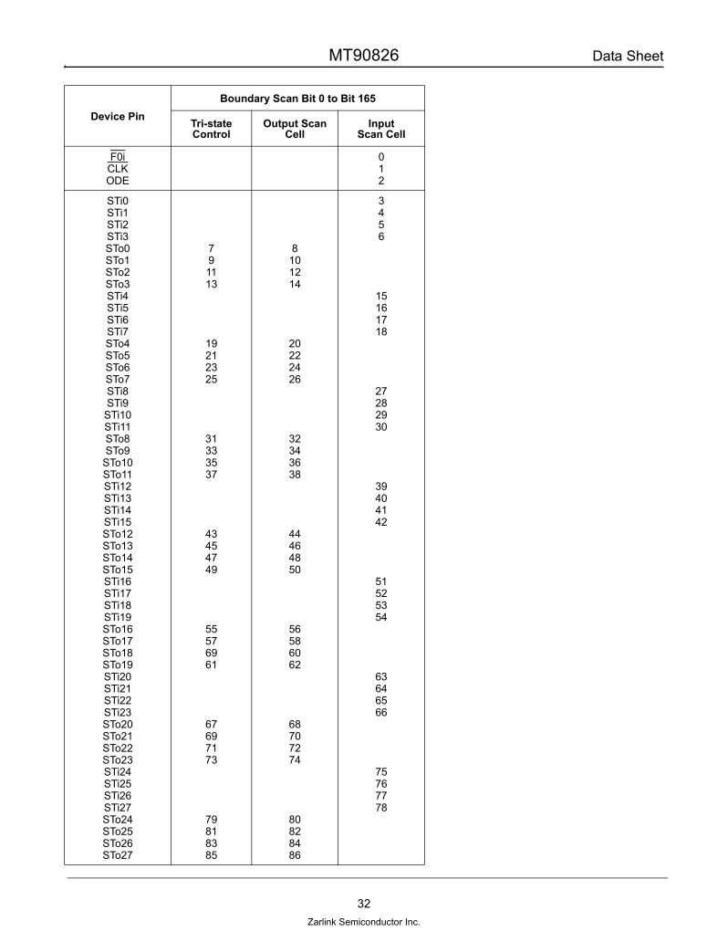
10.0 JTAG SupportThe MT90826 JTAG interface conforms to the Boundary-Scan standard IEEE1149.1. This standard specifies adesign-for-testability technique called Boundary-Scan test (BST). The operation of the boundary-scan circuitry iscontrolled by an external test access port (TAP) Controller.
10.1 Test Access Port (TAP)
The Test Access Port (TAP) provides access to the many test functions of the MT90826. It consists of three inputpins and one output pin. The following pins are from the TAP.
• Test Clock Input (TCK)TCK provides the clock for the test logic. The TCK does not interfere with any on-chip clock and thus remain independent. The TCK permits shifting of test data into or out of the Boundary-Scan register cells concurrently with the operation of the device and without interfering with the on-chip logic.
• Test Mode Select Input (TMS)The logic signals received at the TMS input are interpreted by the TAP Controller to control the test operations. The TMS signals are sampled at the rising edge of the TCK pulse. This pin is internally pulled to Vdd when it is not driven from an external source.
• Test Data Input (TDI)Serial input data applied to this port is fed either into the instruction register or into a test data register, depending on the sequence previously applied to the TMS input. Both registers are described in a subsequent section. The received input data is sampled at the rising edge of TCK pulses. This pin is internally pulled to Vdd when it is not driven from an external source.
• Test Data Output (TDO)Depending on the sequence previously applied to the TMS input, the contents of either the instruction register or data register are serially shifted out towards the TDO. The data out of the TDO is clocked on the falling edge of the TCK pulses. When no data is shifted through the boundary scan cells, the TDO driver is set to a high impedance state.
• Test Reset (TRST)Resets the JTAG scan structure. This pin is internally pulled to VDD.

MT90826 Data Sheet
31Zarlink Semiconductor Inc.
10.2 Instruction Register
In accordance with the IEEE 1149.1 standard, the MT90826 uses public instructions. The JTAG Interface containsa three-bit instruction register. Instructions are serially loaded into the instruction register from the TDI when theTAP Controller is in its shifted-IR state. Subsequently, the instructions are decoded to achieve two basic functions:to select the test data register that may operate while the instruction is current, and to define the serial test dataregister path, which is used to shift data between TDI and TDO during data register scanning.
Test Data Register
As specified in IEEE 1149.1, the MT90826 JTAG Interface contains three test data registers:
• The Boundary-Scan registerThe Boundary-Scan register consists of a series of Boundary-Scan cells arranged to form a scan path around the boundary of the MT90826 core logic.
• The Bypass RegisterThe Bypass register is a single stage shift register that provides a one-bit path from TDI to its TDO.
• The Device Identification RegisterThe device identification register is a 32-bit register with the register contain of:
The LSB bit in the device identification register is the first bit clock out.
The MT90826 scan register contains 165 bits.
MSB LSB
0000 0000 1000 0010 0110 0001 0100 1011
MT90826 Data Sheet
32Zarlink Semiconductor Inc.
Device PinBoundary Scan Bit 0 to Bit 165
Tri-state Control
Output Scan Cell
InputScan Cell
F0iCLKODE
012
STi0STi1STi2STi3STo0STo1STo2STo3STi4STi5STi6STi7STo4STo5STo6STo7STi8STi9
STi10STi11STo8STo9
STo10STo11STi12STi13STi14STi15STo12STo13STo14STo15STi16STi17STi18STi19STo16STo17STo18STo19STi20STi21STi22STi23STo20STo21STo22STo23STi24STi25STi26STi27STo24STo25STo26STo27
791113
19212325
31333537
43454749
55576961
67697173
79818385
8101214
20222426
32343638
44464850
56586062
68707274
80828486
3456
15161718
27282930
39404142
51525354
63646566
75767778

MT90826 Data Sheet
33Zarlink Semiconductor Inc.
Note 1: DTA is an open drain output and it requires a pull-up resistor. Safe for DTA = 0. DTA cell = 1 will produce active LOW.
STi28STi29STi30STi31STo28ST029ST030STo31
91939597
92949698
87888990
D0D1D2D3D4D5D6D7D8D9
D10D11D12D13D14D15
99102105108111114117120123126129132135138141144
100103106109112115118121124127130133136139142145
101104107110113116119122125128131134137140143146
DTA1
CSR/WDS
147 147148149150
A0A1A2A3A4A5A6A7A8A9
A10A11A12A13
RESETb
151152153154155156157158159160161162163164165
Device PinBoundary Scan Bit 0 to Bit 165
Tri-state Control
Output Scan Cell
InputScan Cell

MT90826 Data Sheet
34Zarlink Semiconductor Inc.
Bit Name Description
15-14 TM1-0 Mode Select Bits.
TM1 TM0 Mode Selection 0 0 Variable Throughput Delay mode (Note 1) 1 0 Constant Throughput Delay mode (Note 2) 0 1 Message mode; the contents of the connection memory are output on the corresponding output channel and stream. Only the lower byte (bit 7 - bit 0) will be output to the ST-BUS output pins. 1 1 Bit Error Test mode; the pseudo random test pattern will be output on the output channel and stream associated with this location.
13 OE Output Enable. This bit enables the drivers of STo pins on a per-channel basis. When 1, the STo output driver functions normally. When 0, the STo output driver is in a high-impedance state.
12-8 SAB4-0 Source Stream Address Bits. The binary value is the number of the data stream for the source of the connection.
7-0 CAB7-0 Source Channel Address Bits. The binary value is the number of the channel for the source of the connection. When the message mode is enabled, these entire 8 bits are output on the output channel and stream associated with this location.
Note 1: The Variable delay is only available for odd number output streams but not for the even number output streams. Avoid programming the TM0 and TM1 bits to zero in the connection memory when the destination output streams are STo0, 2, 4, ... , 28 and 30.
Note 2: The constant delay mode is available for all output streams.
Table 14 - Connection Memory Bits
Data Rate SAB4 to SAB0 Bits Used to Determine the Source Stream of the connection
CAB Bits Used to Determine the Source Channel of the Connection
8 Mbps SAB4 to SAB0 (STi0 to STi31) CAB6 to CAB0 (128 channel/frame)
16 Mbps SAB3 to SAB0 (STi0 to STi15) CAB7 to CAB0 (256 channel/frame)
4 Mbps & 8 Mbps SAB4 to SAB0 (STi0 to STi31) CAB6 to CAB0 (64 or 128 channel/frame)
16 Mbps & 8 Mbps SAB4 to SAB0 (STi0 to STi19) CAB7 to CAB0 (128 or 256 channel/frame)
4 Mbps SAB4 to SAB0 (STi0 to STi31) CAB5 to CAB0 (64 channel/frame)
2 Mbps & 4 Mbps SAB4 to SAB0 (STi0 to STi31) CAB5 to CAB0 (32 or 64 channel/frame)
2 Mbps SAB4 to SAB0 (STi0 to STi31) CAB4 to CAB0 (32 channel/frame)
Table 15 - SAB and CAB Bits Programming for Various Interface Mode
7 6 5 4 3 2 1 08910111213
CABCABCABCAB CABCABCABSABSABSAB
14
TM0
15
OETM1 2 1 0 7 6 5 4 3 2 1 0CAB
3SABSAB
4

MT90826 Data Sheet
35Zarlink Semiconductor Inc.
* Exceeding these values may cause permanent damage. Functional operation under these conditions is not implied
Note 1: Maximum leakage on pins (output or I/O pins in high impedance state) is over an applied voltage (V)
Absolute Maximum Ratings*
Parameter Symbol Min. Max. Units
1 Supply Voltage VDD -0.3 5.0 V2 Voltage on any 3.3 V tolerant pin I/O (other than
supply pins)VI VSS - 0.3 VDD + 0.3 V
3 Voltage on any 5 V tolerant pin I/O (other than sup-ply pins)
VI VSS - 0.3 5.0 V
4 Continuous Current at digital outputs Io 20 mA5 Package power dissipation PD 1 W6 Storage temperature TS - 65 +125 °C
Recommended Operating Conditions - Voltages are with respect to ground (Vss) unless otherwise stated.
Characteristics Sym. Min. Typ. Max. Units Test Conditions
1 Operating Temperature TOP -40 +85 °C2 Positive Supply VDD 3.0 3.6 V3 Input High Voltage VIH 0.7VDD VDD V4 Input High Voltage on 5 V Tolerant Inputs VIH 5.5 V5 Input Low Voltage VIL VSS 0.3VDD V
DC Electrical Characteristics - Voltages are with respect to ground (Vss) unless otherwise stated.
Characteristics Sym. Min. Typ. Max. Units Test Conditions
1
INPUTS
Supply Current IDD 64 100 mA Output unloaded2 Input High Voltage VIH 0.7VDD V3 Input Low Voltage VIL 0.3VDD V4 Input Leakage (input pins)
Input Leakage (with pull-up or pull-down)
IILIBL
1550
µAµA 0≤<V≤VDD See Note 1
5 Input Pin Capacitance CI 10 pF6 O
UTPUTS
Output High Voltage VOH 0.8VDD V IOH = 10mA7 Output Low Voltage VOL 0.4 V IOL = 10mA8 High Impedance Leakage IOZ 5 µA 0 < V < VDD See Note 19 Output Pin Capacitance CO 10 pF

MT90826 Data Sheet
36Zarlink Semiconductor Inc.
AC Electrical Characteristics - Timing Parameter Measurement Voltage Levels
Characteristics Sym. Level Units Conditions
1 CMOS Threshold Voltage VTT 0.5VDD V2 CMOS Rise/Fall Threshold Voltage High VHM 0.7VDD V3 CMOS Rise/Fall Threshold Voltage Low VLM 0.3VDD V
AC Electrical Characteristics - Frame Pulse and CLK
Characteristic Sym. Min. Typ. Max. Units CLK
1 Frame pulse width tFPW 55 65 ns16.384 MHz2 Frame Pulse Setup time before CLK falling tFPS 5 ns
3 Frame Pulse Hold Time from CLK falling tFPH 10 ns
4 CLK Period tCP 55 70 ns
5 CLK Pulse Width High tCH 20 40 ns
6 CLK Pulse Width Low tCL 20 40 ns
7 Frame pulse width tFPW8 115 145 ns 8.192 MHz
8 Frame Pulse Setup time before CLK falling tFPS8 5 ns
9 Frame Pulse Hold Time from CLK falling tFPH8 10 ns
10 CLK Period tCP8 110 150 ns
11 CLK Pulse Width High tCH8 50 75 ns
12 CLK Pulse Width Low tCL8 50 75 ns
13 Clock Rise/Fall Time tr, tf 0 +10 ns

MT90826 Data Sheet
37Zarlink Semiconductor Inc.
Note: 1. High Impedance is measured by pulling to the appropriate rail with RL, with timing corrected to cancel time taken to discharge CL
Figure 8 - ST-BUS Timing for Stream rate of 16.384 Mbps
AC Electrical Characteristics - Serial Streams for ST-BUS
Characteristic Sym. Min. Typ. Max. Units Test Conditions
1 Input Data Sample Point (Data rate of 16 Mbps)
tIDS_16 30 ns
2 Input Data Sample Point (Data rate of 8 Mbps)
tIDS_8 91 ns
3 Input Data Sample Point (Data rate of 4 Mbps)
tIDS_4 183 ns
4 Input Data Sample Point (Data rate of 2 Mbps)
tIDS_2 366 ns
5 STi Set-up Time (Data rate of 16 Mbps) tSIS_16 0 ns6 STi Hold Time (Date rate of 16 Mbps) tSIH_16 8 ns7 STi Set-up Time (Date rate of 2, 4 or 8 Mbps) tSIS 0 ns8 STi Hold Time (Date rate of 2, 4 or 8 Mbps) tSIH 8 ns
9 STo Delay - Active to Active tSOD 811
3043
ns CL=30pFCL=200pF
10 Output Driver Enable (ODE) Delay tODE 35 ns RL=1K, CL=200pF, See Note 1
11 STo delay - Active to High-Z - High-Z to Active
tDZ,tZD
35 ns RL=1K, CL=200pF, See Note 1
VTT
VTT
F0i
CLK
tFPW
STo
STi
tFPH
tSOD
tSIH_16
tCH tCL
tFPS
tCP
tSIS_16
VTT
VTT
VHM
VLM
tr
tf
Ch0Bit5
Ch0Bit6
Ch0Bit7
Ch255Bit0
Ch255Bit1
Ch0Bit2
Ch0Bit3
Ch0Bit4
Ch0Bit1
Ch0Bit5
Ch0Bit6
Ch0Bit7
Ch255Bit0
Ch255Bit1
Ch0Bit2
Ch0Bit3
Ch0Bit4
Ch0Bit1
(16.384 MHz)
(16 Mbps)
(16 Mbps)
tIDS_16

MT90826 Data Sheet
38Zarlink Semiconductor Inc.
Figure 9 - ST-BUS Timing for Stream rate of 8.192 Mbps when CLK = 16.384 MHz
Figure 10 - ST-BUS Timing for Stream rate of 4.096 Mbps when CLK = 16.384 MHz
Figure 11 - ST-BUS Timing for Stream rate of 4.096 Mbps when CLK = 8.192 MHz
VTT
VTT
F0i
CLK
tFPW
STo
STi
tFPH
tSOD
tSIH
tCH tCL
Bit 0, Last Channel
tFPS tCP
tSIS
VTT
VTT
Bit 7, Channel 0 Bit 6, Channel 0 Bit 5, Channel 0
Bit 0, Last Channel Bit 7, Channel 0 Bit 6, Channel 0 Bit 5, Channel 0
VHM
VLM
tr
tf(16.384 MHz)
tIDS_8
VTT
VTT
F0i
CLK
tFPW
STo
STi
tFPH
tSOD
tSIH
tCH tCLtFPS tCP
tSIS
VTT
VTT
VHM
VLMtf
Ch0 Bit 7
(16.384 MHz)
(4 Mbps)
(4 Mbps)
Ch0 Bit 6
Ch0 Bit 7 Ch0 Bit 6
Ch63 Bit 0
Ch63 Bit 0
tr
tIDS_4
VTT
VTT
F0i
CLK
tFPW8
STo
STi
tFPH8
tSOD
tSIH
tFPS8 tCP8
tSIS
VTT
VTT
VHM
VLM
Ch0 Bit 7
(8.192 MHz)
(4 Mbps)
(4 Mbps)
Ch0 Bit 6
Ch0 Bit 7 Ch0 Bit 6
Ch63 Bit 0
Ch63 Bit 0
tCH8tCL8 tr
tf

MT90826 Data Sheet
39Zarlink Semiconductor Inc.
Figure 12 - ST-BUS Timing for Stream rate of 2.048 Mbps when CLK = 16.384 MHz
Figure 13 - -BUS Timing for Stream rate of 2.048 Mbps when CLK = 8.192 MHz
Figure 14 - Serial Output and External Control
F0i
CLK
tFPW
tFPH
tSOD
tCH tCLtFPS tCP
VTT
VTT
VHM
VLM
tr
tf
(16.384 MHz)
VTT
VTTSTo
STi
tSIHtSIS
Ch0 Bit 7(2 Mbps)
(2 Mbps)
Ch0 Bit 6
Ch0 Bit 7 Ch0 Bit 6
Ch31 Bit 0
Ch31 Bit 0
tIDS_2
tSOD
VTT
VTTSTo
STi
tSIHtSIS
Ch0 Bit 7(2 Mbps)
(2 Mbps)
Ch0 Bit 6
Ch0 Bit 7 Ch0 Bit 6
Ch31 Bit 0
Ch31 Bit 0
F0i
CLKtFPH8tFPS8 tCP8
VTT
VTT
VHM
VLM(8.192 MHz)
tCH8tCL8
tDZ
STotZD
STo
CLK VTT
VTTHiZValid Data
VTTHiZ Valid Data

MT90826 Data Sheet
40Zarlink Semiconductor Inc.
Figure 15 - Output Driver Enable (ODE)
VTTHiZHiZSTo
ODEtODEtODE
Valid Data
VTT
MT90826 Data Sheet
41Zarlink Semiconductor Inc.
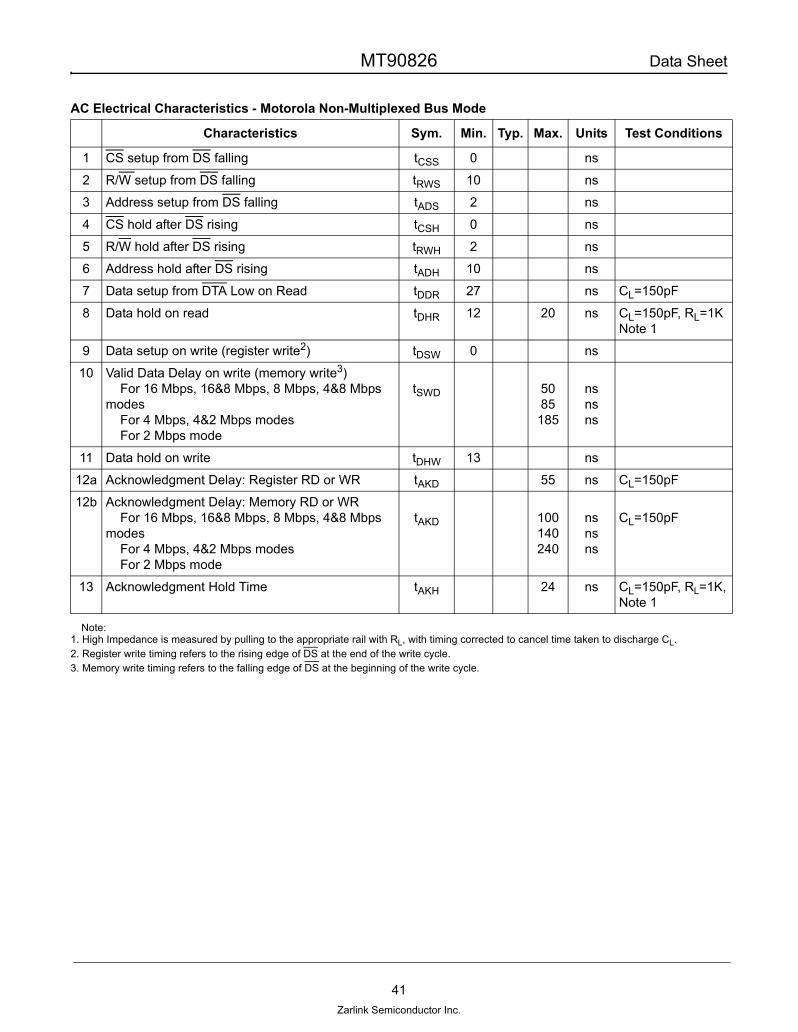
Note:1. High Impedance is measured by pulling to the appropriate rail with RL, with timing corrected to cancel time taken to discharge CL.2. Register write timing refers to the rising edge of DS at the end of the write cycle.3. Memory write timing refers to the falling edge of DS at the beginning of the write cycle.
AC Electrical Characteristics - Motorola Non-Multiplexed Bus Mode
Characteristics Sym. Min. Typ. Max. Units Test Conditions
1 CS setup from DS falling tCSS 0 ns
2 R/W setup from DS falling tRWS 10 ns
3 Address setup from DS falling tADS 2 ns
4 CS hold after DS rising tCSH 0 ns
5 R/W hold after DS rising tRWH 2 ns
6 Address hold after DS rising tADH 10 ns
7 Data setup from DTA Low on Read tDDR 27 ns CL=150pF
8 Data hold on read tDHR 12 20 ns CL=150pF, RL=1KNote 1
9 Data setup on write (register write2) tDSW 0 ns
10 Valid Data Delay on write (memory write3) For 16 Mbps, 16&8 Mbps, 8 Mbps, 4&8 Mbps
modesFor 4 Mbps, 4&2 Mbps modesFor 2 Mbps mode
tSWD 5085185
nsnsns
11 Data hold on write tDHW 13 ns
12a Acknowledgment Delay: Register RD or WR tAKD 55 ns CL=150pF
12b Acknowledgment Delay: Memory RD or WR For 16 Mbps, 16&8 Mbps, 8 Mbps, 4&8 Mbps
modesFor 4 Mbps, 4&2 Mbps modesFor 2 Mbps mode
tAKD 100140240
nsnsns
CL=150pF
13 Acknowledgment Hold Time tAKH 24 ns CL=150pF, RL=1K,Note 1

MT90826 Data Sheet
42Zarlink Semiconductor Inc.
Figure 16 - Motorola Non-Multiplexed Bus Timing
DS
A0-A7
CS
D0-D15
D0-D15
READ
WRITE
tCSS tCSH
tADH
tDHR
tRWS
R/W
tADS
tRWH
tDHW
tAKD
tSWD
tDDR
tAKH
DTA
VTT
VTT
VTT
VTT
VTT
VTT
VTT
tDSW
Valid Address
Valid Read Data
Valid Write Data

c Zarlink S
emiconductor 2002 A
ll rights reserved.
AP
PR
D.
ISS
UE
DA
TE
AC
N
Package C
ode : GA
Previous package codes:
213936
1
20Jan03


c Zarlink Semiconductor 2002 All rights reserved.
APPRD.
ISSUE
DATE
ACN
Package Code
Previous package codes
213740
1
15Nov02
2
213834
11Dec02

www.zarlink.com
Information relating to products and services furnished herein by Zarlink Semiconductor Inc. or its subsidiaries (collectively “Zarlink”) is believed to be reliable.However, Zarlink assumes no liability for errors that may appear in this publication, or for liability otherwise arising from the application or use of any suchinformation, product or service or for any infringement of patents or other intellectual property rights owned by third parties which may result from such application oruse. Neither the supply of such information or purchase of product or service conveys any license, either express or implied, under patents or other intellectualproperty rights owned by Zarlink or licensed from third parties by Zarlink, whatsoever. Purchasers of products are also hereby notified that the use of product incertain ways or in combination with Zarlink, or non-Zarlink furnished goods or services may infringe patents or other intellectual property rights owned by Zarlink.
This publication is issued to provide information only and (unless agreed by Zarlink in writing) may not be used, applied or reproduced for any purpose nor form partof any order or contract nor to be regarded as a representation relating to the products or services concerned. The products, their specifications, services and otherinformation appearing in this publication are subject to change by Zarlink without notice. No warranty or guarantee express or implied is made regarding thecapability, performance or suitability of any product or service. Information concerning possible methods of use is provided as a guide only and does not constituteany guarantee that such methods of use will be satisfactory in a specific piece of equipment. It is the user’s responsibility to fully determine the performance andsuitability of any equipment using such information and to ensure that any publication or data used is up to date and has not been superseded. Manufacturing doesnot necessarily include testing of all functions or parameters. These products are not suitable for use in any medical products whose failure to perform may result insignificant injury or death to the user. All products and materials are sold and services provided subject to Zarlink’s conditions of sale which are available on request.
Purchase of Zarlink’s I2C components conveys a licence under the Philips I2C Patent rights to use these components in and I2C System, provided that the systemconforms to the I2C Standard Specification as defined by Philips.
Zarlink, ZL and the Zarlink Semiconductor logo are trademarks of Zarlink Semiconductor Inc.
Copyright Zarlink Semiconductor Inc. All Rights Reserved.
TECHNICAL DOCUMENTATION - NOT FOR RESALE
For more information about all Zarlink productsvisit our Web Site at