Embed Size (px)
Citation preview

1Zarlink Semiconductor Inc.
Zarlink, ZL and the Zarlink Semiconductor logo are trademarks of Zarlink Semiconductor Inc.Copyright 1997-2005, Zarlink Semiconductor Inc. All Rights Reserved.
Features• 2.7 - 3.6 volt operation
• Complete DTMF receiver
• Low power consumption
• Internal gain setting amplifier
• Adjustable guard time
• Central office quality
• Power-down mode
• Inhibit mode
• Functionally compatible with Zarlink’s MT8870D
Applications• Paging systems
• Repeater systems/mobile radio
• Credit card systems
• Remote control
• Personal computers
• Telephone answering machine
DescriptionThe MT88L70 is a complete 3 Volt, DTMF receiverintegrating both the bandsplit filter and digital decoderfunctions. The filter section uses switched capacitortechniques for high and low group filters; the decoderuses digital counting techniques to detect and decodeall 16 DTMF tone-pairs into a 4-bit code. Externalcomponent count is minimized by on chip provision ofa differential input amplifier, clock oscillator and latchedthree-state bus interface.
August 2005
Ordering Information
MT88L70AE 18 Pin PDIP TubesMT88L70AS 18 Pin SOIC TubesMT88L70AN 20 Pin SSOP TubesMT88L70ASR 18 Pin SOIC Tape & ReelMT88L70ANR 20 Pin SSOP Tape & ReelMT88L70AE1 18 Pin PDIP* TubesMT88L70AN1 20 Pin SSOP* TubesMT88L70ANR1 20 Pin SSOP* Tape & ReelMT88L70AS1 18 Pin SOIC* TubesMT88L70ASR1 18 Pin SOIC* Tape & Reel
* Pb Free Matte Tin-40°C to +85°C
MT88L70 3 Volt Integrated DTMF Receiver
Data Sheet
Figure 1 - Functional Block Diagram
PWDN
IN +
IN -
GS
OSC1 OSC2 St/GT ESt STD TOE
Q1
Q2
Q3
Q4
VDD VSS VRef INH
BiasCircuit
DialToneFilter
High GroupFilter
Low GroupFilter
DigitalDetectionAlgorithm
CodeConverterand Latch
StGT
SteeringLogic
ChipPower
ChipBias
VRefBuffer
Zero CrossingDetectors
to allChipClocks

MT88L70 Data Sheet
2Zarlink Semiconductor Inc.
Figure 2 - Pin Connections
Pin Description
Pin #Name Description
18 20
1 1 IN+ Non-Inverting Op-Amp (Input).
2 2 IN- Inverting Op-Amp (Input).
3 3 GS Gain Select. Gives access to output of front end differential amplifier for connection of feedback resistor.
4 4 VRef Reference Voltage (Output). Nominally VDD/2 is used to bias inputs at mid-rail (see Figure 5 and Figure 6).
5 5 INH Inhibit (Input). Logic high inhibits the detection of tones representing characters A, B, C and D. This pin input is internally pulled down.
6 6 PWDN Power Down (Input). Active high. Powers down the device and inhibits the oscillator. This pin input is internally pulled down.
7 8 OSC1 Clock (Input).
8 9 OSC2 Clock (Output). A 3.579545 MHz crystal connected between pins OSC1 and OSC2 completes the internal oscillator circuit.
9 10 VSS Ground (Input). 0 V typical.
10 11 TOE Three State Output Enable (Input). Logic high enables the outputs Q1-Q4. This pin is pulled up internally.
11-14
12-15
Q1-Q4 Three State Data (Output). When enabled by TOE, provide the code corresponding to the last valid tone-pair received (see Table 1). When TOE is logic low, the data outputs are high impedance.
15 17 StD Delayed Steering (Output).Presents a logic high when a received tone-pair has been registered and the output latch updated; returns to logic low when the voltage on St/GT falls below VTSt.
16 18 ESt Early Steering (Output). Presents a logic high once the digital algorithm has detected a valid tone pair (signal condition). Any momentary loss of signal condition will cause ESt to return to a logic low.
123456789 10
1817161514131211
IN+IN-GS
VRefINH
PWDNOSC1OSC2
VSS
VDDSt/GTEStStDQ4Q3Q2Q1TOE
18 PIN PDIP/SOIC
123456789
10 1112
2019181716151413
IN+IN-GS
VRefINH
PWDNNC
OSC1OSC2
VSS
20 PIN SSOP
VDDSt/GTEStStD
Q4Q3Q2Q1TOE
NC
MT88L70 Data Sheet
3Zarlink Semiconductor Inc.
Functional DescriptionThe MT88L70 monolithic DTMF receiver offers small size, low power consumption and high performance, with 3volt operation. Its architecture consists of a bandsplit filter section, which separates the high and low group tones,followed by a digital counting section which verifies the frequency and duration of the received tones before passingthe corresponding code to the output bus.
Filter Section
Separation of the low-group and high group tones is achieved by applying the DTMF signal to the inputs of twosixth-order switched capacitor bandpass filters, the bandwidths of which correspond to the low and high groupfrequencies. The filter section also incorporates notches at 350 and 440 Hz for exceptional dial tone rejection. Eachfilter output is followed by a single order switched capacitor filter section which smooths the signals prior to limiting.Limiting is performed by high-gain comparators which are provided with hysteresis to prevent detection ofunwanted low-level signals. The outputs of the comparators provide full rail logic swings at the frequencies of theincoming DTMF signals.
Decoder Section
Following the filter section is a decoder employing digital counting techniques to determine the frequencies of theincoming tones and to verify that they correspond to standard DTMF frequencies. A complex averaging algorithmprotects against tone simulation by extraneous signals such as voice while providing tolerance to small frequencydeviations and variations. This averaging algorithm has been developed to ensure an optimum combination ofimmunity to talk-off and tolerance to the presence of interfering frequencies (third tones) and noise. When thedetector recognizes the presence of two valid tones (this is referred to as the “signal condition” in some industryspecifications) the “Early Steering” (ESt) output will go to an active state. Any subsequent loss of signal conditionwill cause ESt to assume an inactive state (see “Steering Circuit”).
Steering Circuit
Before registration of a decoded tone pair, the receiver checks for a valid signal duration (referred to as characterrecognition condition). This check is performed by an external RC time constant driven by ESt. A logic high on EStcauses vc (see Figure 3) to rise as the capacitor discharges. Provided signal condition is maintained (ESt remainshigh) for the validation period (tGTP), vc reaches the threshold (VTSt) of the steering logic to register the tone pair,latching its corresponding 4-bit code (see Table 1) into the output latch. At this point the GT output is activated anddrives vc to VDD. GT continues to drive high as long as ESt remains high. Finally, after a short delay to allow theoutput latch to settle, the delayed steering output flag (StD) goes high, signalling that a received tone pair has beenregistered. The contents of the output latch are made available on the 4-bit output bus by raising the three statecontrol input (TOE) to a logic high. The steering circuit works in reverse to validate the interdigit pause betweensignals. Thus, as well as rejecting signals too short to be considered valid, the receiver will tolerate signalinterruptions (dropout) too short to be considered a valid pause. This facility, together with the capability of selecting
17 19 St/GT Steering Input/Guard time (Output) Bidirectional. A voltage greater than VTSt detected at St causes the device to register the detected tone pair and update the output latch. A voltage less than VTSt frees the device to accept a new tone pair. The GT output acts to reset the external steering time-constant; its state is a function of ESt and the voltage on St.
18 20 VDD Positive power supply (Input). +3 V typical.
7, 16 NC No Connection.
Pin Description
Pin #Name Description
18 20

MT88L70 Data Sheet
4Zarlink Semiconductor Inc.
the steering time constants externally, allows the designer to tailor performance to meet a wide variety of systemrequirements.
Table 1 - Functional Decode TableL=LOGIC LOW, H=LOGIC HIGH, Z=HIGH IMPEDANCEX = DON‘T CARE
Guard Time Adjustment
In many situations not requiring selection of tone duration and interdigital pause, the simple steering circuit shownin Figure 3 is applicable. Component values are chosen according to the formula:
tREC=tDP+tGTPtID=tDA+tGTA
The value of tDP is a device parameter (see Figure 7) and tREC is the minimum signal duration to be recognized bythe receiver. A value for C of 0.1 µF is recommended for most applications, leaving R to be selected by thedesigner.
Digit TOE INH ESt Q4 Q3 Q2 Q1
ANY L X H Z Z Z Z
1 H X H 0 0 0 1
2 H X H 0 0 1 0
3 H X H 0 0 1 1
4 H X H 0 1 0 0
5 H X H 0 1 0 1
6 H X H 0 1 1 0
7 H X H 0 1 1 1
8 H X H 1 0 0 0
9 H X H 1 0 0 1
0 H X H 1 0 1 0
* H X H 1 0 1 1
# H X H 1 1 0 0
A H L H 1 1 0 1
B H L H 1 1 1 0
C H L H 1 1 1 1
D H L H 0 0 0 0
A H H Lundetected, the output code will remain the same as the previous detected code
B H H L
C H H L
D H H L

MT88L70 Data Sheet
5Zarlink Semiconductor Inc.
Figure 3 - Basic Steering Circuit
Different steering arrangements may be used to select independently the guard times for tone present (tGTP) andtone absent (tGTA). This may be necessary to meet system specifications which place both accept and reject limitson both tone duration and interdigital pause. Guard time adjustment also allows the designer to tailor systemparameters such as talk off and noise immunity. Increasing tREC improves talk-off performance since it reduces theprobability that tones simulated by speech will maintain signal condition long enough to be registered. Alternatively,a relatively short tREC with a long tDO would be appropriate for extremely noisy environments where fast acquisitiontime and immunity to tone drop-outs are required. Design information for guard time adjustment is shown in Figure4.
Power-down and Inhibit Mode
A logic high applied to pin 6 (PWDN) will power down the device to minimize the power consumption in a standbymode. It stops the oscillator and the functions of the filters.
Inhibit mode is enabled by a logic high input to the pin 5 (INH). It inhibits the detection of tones representingcharacters A, B, C, and D. The output code will remain the same as the previous detected code (see Table 1).
Figure 4 - Guard Time Adjustment
C
vc
VDD
St/GT
ESt
StD
MT88L70
R
tGTA=(RC)In(VDD/VTSt)
tGTP=(RC)In[VDD/(VDD-VTSt)]
VDD
VDD
St/GT
ESt
R1
C1
R2
VDD
St/GT
ESt
C1
R1 R2
a) decreasing tGTP; (tGTP < tGTA)
b) decreasing tGTA; (tGTP > tGTA)
tGTA=(R1C1) In (VDD / VTSt)
tGTP=(RPC1) In [VDD / (VDD-VTSt)]
RP = (R1R2) / (R1 + R2)
tGTA=(RPC1) In (VDD / VTSt)
tGTP=(R1C1) In [VDD / (VDD-VTSt)]
RP = (R1R2) / (R1 + R2)

MT88L70 Data Sheet
6Zarlink Semiconductor Inc.
Differential Input Configuration
The input arrangement of the MT88L70 provides a differential-input operational amplifier as well as a bias source(VRef) which is used to bias the inputs at mid-rail. Provision is made for connection of a feedback resistor to the op-amp output (GS) for adjustment of gain. In a single-ended configuration, the input pins are connected as shown inFigure 6 with the op-amp connected for unity gain and VRef biasing the input at 1/2VDD. Figure 5 shows thedifferential configuration, which permits the adjustment of gain with the feedback resistor R5.
Figure 5 - Differential Input Configuration
Crystal Oscillator
The internal clock circuit is completed with the addition of an external 3.579545 MHz crystal and is connected asshown in Figure 6 (Single-ended Input Configuration).
C1 R1
C2 R4
IN+
IN-
R5R2
R3
GS
VRef
+
-
MT88L70
DIFFERNTIAL INPUT AMPLIFIERC1 = C2 = 10 nFR1 = R4 = R5 = 100 kΩR2 = 60 kΩ, R3, = 37.5 kΩ
R3 = R2R5R2 + R5
VOLTAGE GAIN (AV diff) = R5R1
INPUT IMPEDANCE
(ZINDIFF) = 2 R12 + 1
ωC
2
All resistors are ± 1% tolerance.All capacitors are ± 5% tolerance.
MT88L70 Data Sheet
7Zarlink Semiconductor Inc.
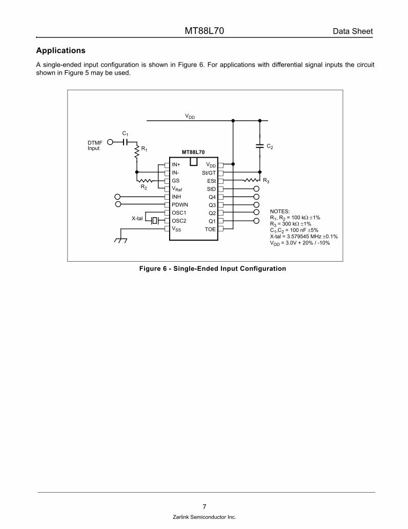
ApplicationsA single-ended input configuration is shown in Figure 6. For applications with differential signal inputs the circuitshown in Figure 5 may be used.
Figure 6 - Single-Ended Input Configuration
IN+IN-GSVRef
INHPDWNOSC1OSC2VSS
VDD
St/GTEStStDQ4Q3Q2Q1
TOE
DTMFInput
C1
VDD
R1
R2
X-tal
MT88L70C2
R3
NOTES:R1, R2 = 100 kΩ ±1%R3 = 300 kΩ ±1%C1,C2 = 100 nF ±5%X-tal = 3.579545 MHz ±0.1%VDD = 3.0V + 20% / -10%

MT88L70 Data Sheet
8Zarlink Semiconductor Inc.
† Exceeding these values may cause permanent damage. Functional operation under these conditions is not implied.Derate above 75 °C at 16 mW / °C. All leads soldered to board.
‡ Typical figures are at 25°C and are for design aid only: not guaranteed and not subject to production testing.
Absolute Maximum Ratings†
Parameter Symbol Min. Max. Units
1 DC Power Supply Voltage VDD 7 V
2 Voltage on any pin VI VSS-0.3 VDD+0.3 V
3 Current at any pin (other than supply) II 10 mA
4 Storage temperature TSTG -65 +150 °C
5 Package power dissipation PD 500 mW
Recommended Operating Conditions - Voltages are with respect to ground (VSS) unless otherwise stated.
Parameter Sym. Min. Typ.‡ Max. Units Test Conditions
1 DC Power Supply Voltage VDD 2.7 3.0 3.6 V
2 Operating Temperature TO -40 +85 °C
3 Crystal/Clock Frequency fc 3.579545 MHz
4 Crystal/Clock Freq.Tolerance ∆fc ±0.1 %
DC Electrical Characteristics - VDD = 3.0 V+ 20%/-10%, VSS = 0 V, -40°C ≤ TO ≤ +85°C, unless otherwise stated.
Characteristics Sym. Min. Typ.‡ Max. Units Test Conditions
1 SUPPLY
Standby supply current IDDQ 1 10 µA PWDN=VDD
2 Operating supply current IDD 2.0 5.5 mA
3 Power consumption PO 6 mW fc=3.579545 MHz
4
INPUTS
High level input VIH 2.1 V VDD = 3.0 V
5 Low level input voltage VIL 0.9 V VDD = 3.0 V
6 Input leakage current IIH/IIL 0.05 5 µA VIN = VSS or VDD
7 Pull up (source) current ISO 4 15 µA TOE (pin 10) = 0, VDD = 3.0 V
8 Pull down (sink) current ISI 15 40 µA INH = VDD, PWDN = VDD, VDD = 3.0 V
9 Input impedance (IN+, IN-) RIN 10 MΩ @ 1 kHz
10 Steering threshold voltage VTSt 0.465VDD V

MT88L70 Data Sheet
9Zarlink Semiconductor Inc.
‡ Typical figures are at 25°C and are for design aid only: not guaranteed and not subject to production testing.
11
OUTPUTS
Low level output voltage VOL VSS+0.03 V No load
12 High level output voltage VOH VDD-0.03 V No load
13 Output low (sink) current IOL 1.5 8 mA VOUT = 0.4 V
14 Output high (source) current
IOH 1.0 3.0 mA VOUT = 3.6 V,VDD = 3.6 V
15 VRef output voltage VRef 0.512VDD V No load
16 VRef output resistance ROR 1 kΩ
Operating Characteristics - VDD = 3.0 V+20%/-10%, VSS = 0 V, -40°C ≤ TO ≤ +85°C, unless otherwise stated.Gain Setting Amplifier
Characteristics Sym. Min. Typ.‡ Max. Units Test Conditions
1 Input leakage current IIN 100 nA VSS ≤ VIN ≤ VDD
2 Input resistance RIN 10 MΩ
3 Input offset voltage VOS 25 mV
4 Power supply rejection PSRR 50 dB 1 kHz
5 Common mode rejection CMRR 40 dB VSS + 0.75 V ≤ VIN ≤VDD-0.75biased at VRef =1.5 V
6 DC open loop voltage gain AVOL 32 dB
7 Unity gain bandwidth fC 0.30 MHz
8 Output voltage swing VO 2.2 Vpp Load ≥ 100 kΩ to VSS @ GS
9 Maximum capacitive load (GS) CL 100 pF
10 Resistive load (GS) RL 50 kΩ
11 Common mode range VCM 1.5 Vpp No Load
DC Electrical Characteristics - VDD = 3.0 V+ 20%/-10%, VSS = 0 V, -40°C ≤ TO ≤ +85°C, unless otherwise stated.
Characteristics Sym. Min. Typ.‡ Max. Units Test Conditions

MT88L70 Data Sheet
10Zarlink Semiconductor Inc.
‡ Typical figures are at 25 °C and are for design aid only: not guaranteed and not subject to production testing.
*NOTES 1. dBm= decibels above or below a reference power of 1 mW into a 600 ohm load. 2. Digit sequence consists of all DTMF tones. 3. Tone duration= 40 ms, tone pause= 40 ms. 4. Signal condition consists of nominal DTMF frequencies. 5. Both tones in composite signal have an equal amplitude. 6. Tone pair is deviated by ±1.5%± 2 Hz. 7. Bandwidth limited (3 kHz) Gaussian noise. 8. The precise dial tone frequencies are (350 Hz and 440 Hz) ± 2%. 9. For an error rate of better than 1 in 10,000.10. Referenced to lowest level frequency component in DTMF signal.11. Referenced to the minimum valid accept level.12. Guaranteed by design and characterization.
AC Electrical Characteristics - VDD = 3.0 V +20%/-10%, VSS = 0 V, -40°C ≤ TO ≤ +85°C, using Test Circuit shown in Fig. 6.
Characteristics Sym Min. Typ‡ Max Units Notes*
1 Valid input signal levels (each tone of composite signal)
-3415.4
-4.0489
dBmmVRMS
1,2,3,5,6,9Min @ VDD=3.6 VMax @ VDD=2.7 V
2 Negative twist accept 8 dB 2,3,6,9,12
3 Positive twist accept 8 dB 2,3,6,9,12
4 Frequency deviation accept ±1.5% ± 2 Hz 2,3,5,9
5 Frequency deviation reject ±3.5% 2,3,5,9
6 Third zone tolerance -16 dB 2,3,4,5,9,10
7 Noise tolerance -12 dB 2,3,4,5,7,9,10
8 Dial zone tolerance +22 dB 2,3,4,5,8,9,11

MT88L70 Data Sheet
11Zarlink Semiconductor Inc.
‡ Typical figures are at 25°C and are for design aid only: not guaranteed and not subject to production testing.
*NOTES:1. Used for guard-time calculation purposes only and tested at -4 dBm.2. These, user adjustable parameters, are not device specifications. The adjustable settings of these minimums and maximums are
recommendations based upon network requirements.3. With valid tone present at input, tPU equals time from PDWN going low until ESt going high.
AC Electrical Characteristics - VDD = 3.0 V+20%/-10%, VSS = 0 V, -40°C ≤ To ≤ +85°C, using Test Circuit shown in Figure 6.
Characteristics Sym. Min. Typ.‡ Max. Units Conditions
1
TIMING
Tone present detect time tDP 5 11 14 ms Note 1
2 Tone absent detect time tDA 0.5 4 8.5 ms Note 1
3 Tone duration accept tREC 40 ms Note 2
4 Tone duration reject tREC 20 ms Note 2
5 Interdigit pause accept tID 40 ms Note 2
6 Interdigit pause reject tDO 20 ms Note 2
7
OUTPUTS
Propagation delay (St to Q) tPQ 11 µs TOE=VDD
8 Propagation delay (St to StD) tPStD 20 µs TOE=VDD
9 Output data set up (Q to StD) tQStD 5.0 µs TOE=VDD
10 Propagation delay (TOE to Q ENABLE) tPTE 50 ns load of 10 kΩ,50 pF
11 Propagation delay (TOE to Q DISABLE) tPTD 130 ns load of 10 kΩ,50 pF
12 PDWN
Power-up time tPU 30 ms Note 3
13 Power-down time tPD 20 ms
14CLOCK
Crystal/clock frequency fC 3.5759 3.5795 3.5831 MHz
15 Clock input rise time tLHCL 110 ns Ext. clock
16 Clock input fall time tHLCL 110 ns Ext. clock
17 Clock input duty cycle DCCL 40 50 60 % Ext. clock
18 Capacitive load (OSC2) CLO 15 pF

MT88L70 Data Sheet
12Zarlink Semiconductor Inc.
Figure 7 - Timing Diagram
EXPLANATION OF EVENTSA) TONE BURSTS DETECTED, TONE DURATION INVALID, OUTPUTS NOT UPDATED. B) TONE #n DETECTED, TONE DURATION VALID, TONE DECODED AND LATCHED IN OUTPUTS.C) END OF TONE #n DETECTED, TONE ABSENT DURATION VALID, OUTPUTS REMAIN LATCHED UNTIL NEXT VALID
TONE.D) OUTPUTS SWITCHED TO HIGH IMPEDANCE STATE.E) TONE #n+1 DETECTED, TONE DURATION VALID, TONE DECODED AND LATCHED IN OUTPUTS (CURRENTLY
HIGH IMPEDANCE).F) ACCEPTABLE DROPOUT OF TONE #n+1, TONE ABSENT DURATION INVALID, OUTPUTS REMAIN LATCHED.G) END OF TONE #n+1 DETECTED, TONE ABSENT DURATION VALID, OUTPUTS REMAIN LATCHED UNTIL NEXT
VALID TONE.
EXPLANATION OF SYMBOLSVin DTMF COMPOSITE INPUT SIGNAL.ESt EARLY STEERING OUTPUT. INDICATES DETECTION OF VALID TONE FREQUENCIES.St/GT STEERING INPUT/GUARD TIME OUTPUT. DRIVES EXTERNAL RC TIMING CIRCUIT.Q1-Q4 4-BIT DECODED TONE OUTPUT.StD DELAYED STEERING OUTPUT. INDICATES THAT VALID FREQUENCIES HAVE BEEN PRESENT/ABSENT FOR THE
REQUIRED GUARD TIME THUS CONSTITUTING A VALID SIGNAL.TOE TONE OUTPUT ENABLE (INPUT). A LOW LEVEL SHIFTS Q1-Q4 TO ITS HIGH IMPEDANCE STATE.tREC MAXIMUM DTMF SIGNAL DURATION NOT DETECTED AS VALID.tREC MINIMUM DTMF SIGNAL DURATION REQUIRED FOR VALID RECOGNITION.tID MINIMUM TIME BETWEEN VALID DTMF SIGNALS.tDO MAXIMUM ALLOWABLE DROP OUT DURING VALID DTMF SIGNAL.tDP TIME TO DETECT THE PRESENCE OF VALID DTMF SIGNALS.tDA TIME TO DETECT THE ABSENCE OF VALID DTMF SIGNALS.tGTP GUARD TIME, TONE PRESENT.tGTA GUARD TIME, TONE ABSENT.
Vin
ESt
St/GT
Q1-Q4
StD
TOE
EVENTS A B C
D
E F G
tREC tREC tID tDO
TONE #n TONE#n + 1
TONE#n + 1
tDP tDA
tGTP tGTA
tPQtQStD
tPSrD
tPTD
tPTE
# n # (n + 1)HIGH IMPEDANCE
DECODED TONE # (n-1)
VTSt


www.zarlink.com
Information relating to products and services furnished herein by Zarlink Semiconductor Inc. or its subsidiaries (collectively “Zarlink”) is believed to be reliable.However, Zarlink assumes no liability for errors that may appear in this publication, or for liability otherwise arising from the application or use of any suchinformation, product or service or for any infringement of patents or other intellectual property rights owned by third parties which may result from such application oruse. Neither the supply of such information or purchase of product or service conveys any license, either express or implied, under patents or other intellectualproperty rights owned by Zarlink or licensed from third parties by Zarlink, whatsoever. Purchasers of products are also hereby notified that the use of product incertain ways or in combination with Zarlink, or non-Zarlink furnished goods or services may infringe patents or other intellectual property rights owned by Zarlink.
This publication is issued to provide information only and (unless agreed by Zarlink in writing) may not be used, applied or reproduced for any purpose nor form partof any order or contract nor to be regarded as a representation relating to the products or services concerned. The products, their specifications, services and otherinformation appearing in this publication are subject to change by Zarlink without notice. No warranty or guarantee express or implied is made regarding thecapability, performance or suitability of any product or service. Information concerning possible methods of use is provided as a guide only and does not constituteany guarantee that such methods of use will be satisfactory in a specific piece of equipment. It is the user’s responsibility to fully determine the performance andsuitability of any equipment using such information and to ensure that any publication or data used is up to date and has not been superseded. Manufacturing doesnot necessarily include testing of all functions or parameters. These products are not suitable for use in any medical products whose failure to perform may result insignificant injury or death to the user. All products and materials are sold and services provided subject to Zarlink’s conditions of sale which are available on request.
Purchase of Zarlink’s I2C components conveys a licence under the Philips I2C Patent rights to use these components in and I2C System, provided that the systemconforms to the I2C Standard Specification as defined by Philips.
Zarlink, ZL and the Zarlink Semiconductor logo are trademarks of Zarlink Semiconductor Inc.
Copyright Zarlink Semiconductor Inc. All Rights Reserved.
TECHNICAL DOCUMENTATION - NOT FOR RESALE
For more information about all Zarlink productsvisit our Web Site at


![[MS-DTMF]: RTP Payload for DTMF Digits, Telephony Tones](https://img.dokumen.tips/doc/110x75/618761294ef0486d5b31de99/ms-dtmf-rtp-payload-for-dtmf-digits-telephony-tones-.jpg)