Embed Size (px)
Citation preview

MT6226 GSM/GPRS Baseband Processor Data Sheet
Revision 1.00
Sep 16, 2005

MT6226 GSM/GPRS Baseband Processor Data Sheet Revision 1.00
2/463 MediaTek Inc. Confidential
Revision History
Revision Date Comments
1.00 Sep 16, 2005 First Release

MT6226 GSM/GPRS Baseband Processor Data Sheet Revision 1.00
3/463 MediaTek Inc. Confidential
TABLE OF CONTENTS Revision History...................................................................................................................................... 2
Preface...................................................................................................................................................... 5
1. System Overview............................................................................................................................... 6 1.1 Platform Feature......................................................................................................................................................... 9 1.2 MODEM Features.....................................................................................................................................................11 1.3 Multi-Media Features............................................................................................................................................... 12 1.4 General Description ................................................................................................................................................. 14
2 Product Description........................................................................................................................ 16 2.1 Pin Outs.................................................................................................................................................................... 16 2.2 Top Marking Definition ........................................................................................................................................... 19 2.3 DC Characteristics ................................................................................................................................................... 20 2.4 Pin Description......................................................................................................................................................... 21 2.5 Power Description.................................................................................................................................................... 29
3 Micro-Controller Unit Subsystem................................................................................................. 35 3.1 Processor Core ......................................................................................................................................................... 36 3.2 Memory Management .............................................................................................................................................. 36 3.3 Bus System............................................................................................................................................................... 39 3.4 Direct Memory Access............................................................................................................................................. 43 3.5 Interrupt Controller .................................................................................................................................................. 59 3.6 Internal Memory Interface ....................................................................................................................................... 70 3.7 External Memory Interface ...................................................................................................................................... 71
4 Microcontroller Peripherals .......................................................................................................... 79 4.1 Pulse-Width Modulation Outputs............................................................................................................................. 79 4.2 Alerter ...................................................................................................................................................................... 81 4.3 SIM Interface ........................................................................................................................................................... 84 4.4 Keypad Scanner ....................................................................................................................................................... 92 4.5 General Purpose Inputs/Outputs .............................................................................................................................. 95 4.6 General Purpose Timer........................................................................................................................................... 107 4.7 UART......................................................................................................................................................................110 4.8 IrDA Framer........................................................................................................................................................... 124 4.9 Real Time Clock .................................................................................................................................................... 131 4.10 Auxiliary ADC Unit ............................................................................................................................................... 137 4.11 I2C / SCCB ............................................................................................................................................................ 139
5 Microcontroller Coprocessors ..................................................................................................... 145 5.1 Divider ................................................................................................................................................................... 145 5.2 CSD Accelerator .................................................................................................................................................... 147 5.3 FCS Codec ............................................................................................................................................................. 157
6 Multi-Media Subsystem ............................................................................................................... 160 6.1 LCD Interface ........................................................................................................................................................ 160 6.2 JPEG Decoder........................................................................................................................................................ 176 6.3 Image Resizer......................................................................................................................................................... 187 6.4 NAND FLASH interface ....................................................................................................................................... 203 6.5 USB Device Controller .......................................................................................................................................... 219 6.6 Memory Stick and SD Memory Card Controller ................................................................................................... 228 6.7 Graphic Memory Controller................................................................................................................................... 251 6.8 2D acceleration ...................................................................................................................................................... 254 6.9 JPEG Encoder ........................................................................................................................................................ 264

MT6226 GSM/GPRS Baseband Processor Data Sheet Revision 1.00
4/463 MediaTek Inc. Confidential
6.10 Camera Interface .................................................................................................................................................... 268 6.11 Image DMA ........................................................................................................................................................... 315 6.12 Image Engine ......................................................................................................................................................... 334 6.13 MPEG-4/H.263 Video CODEC ............................................................................................................................. 350
7 Audio Front-end............................................................................................................................ 364 7.1 General Description ............................................................................................................................................... 364 7.2 Register Definitions ............................................................................................................................................... 367 7.3 Programming Guide ............................................................................................................................................... 370
8 Radio Interface Control ............................................................................................................... 372 8.1 Baseband Serial Interface....................................................................................................................................... 372 8.2 Baseband Parallel Interface.................................................................................................................................... 377 8.3 Automatic Power Control (APC) Unit ................................................................................................................... 380 8.4 Automatic Frequency Control (AFC) Unit ............................................................................................................ 386
9 Baseband Front End..................................................................................................................... 390 9.1 Baseband Serial Ports............................................................................................................................................. 391 9.2 Downlink Path (RX Path) ...................................................................................................................................... 392 9.3 Uplink Path (TX Path) ........................................................................................................................................... 398
10 Timing Generator ......................................................................................................................... 401 10.1 TDMA timer........................................................................................................................................................... 401 10.2 Slow Clocking Unit................................................................................................................................................ 408
11 Power, Clocks and Reset .............................................................................................................. 410 11.1 B2PSI ..................................................................................................................................................................... 410 11.2 Clocks .................................................................................................................................................................... 412 11.3 Reset Generation Unit (RGU)................................................................................................................................ 417 11.4 Software Power Down Control .............................................................................................................................. 420
12 Analog Front-end & Analog Blocks ............................................................................................ 424 12.1 General Description ............................................................................................................................................... 424 12.2 MCU Register Definitions ..................................................................................................................................... 435 12.3 Programming Guide ............................................................................................................................................... 447
13 Digital Pin Electrical Characteristics.......................................................................................... 459

MT6226 GSM/GPRS Baseband Processor Data Sheet Revision 1.00
5/463 MediaTek Inc. Confidential
Preface
Acronym for Register Type
R/W Capable of both read and write access
RO Read only
RC Read only. After reading the register bank, each bit which is HIGH(1) will be cleared to LOW(0 ) automatically.
WO Write only
W1S Write only. When writing data bits to register bank, each bit which is HIGH(1) will cause the corresponding bit to be set to 1. Data bits which are LOW(0) has no effect on the corresponding bit.
W1C Write only. When writing data bits to register bank, each bit which is HIGH(1) will cause the corresponding bit to be cleared to 0. Data bits which are LOW(0) has no effect on the corresponding bit.

MT6226 GSM/GPRS Baseband Processor Data Sheet Revision 1.00
6/463 MediaTek Inc. Confidential
1. System Overview
The revolutionary MT6226 is a leading edge single-chip solution for GSM/GPRS mobile phones targeting the emerging applications in digital audio and video. Based on 32-bit ARM7EJ-STM RISC processor, MT6226 not only features high performance GPRS Class 12 MODEM, but also provides comprehensive and advanced solutions for handheld multi-media.
Typical application is shown in Figure 1.
Multi-media Subsystem
The MT6226 multi-media subsystem provides connection to CMOS/CCD image sensor and supports resolution up to VGA. With its advanced image signal and data processing technology, MT6226 allows efficient processing of image and video data. It also has built-in JPEG CODEC and MPEG-4/H.263 CODEC, thus enabling real-time creation and playback of high-quality images and video. In addition to advanced image and video features, MT6226 also utilizes high resolution DAC, digital audio, and audio synthesis technology to provide superior audio features for all future multi-media needs.
In order to provide more flexibility and bandwidth for multi-media products, an additional 18-bit parallel interface is incorporated. This interface enables connection to LCD modules as well as connection to NAND flash devices to allow for multi-media data storage capabilities.
External Memory Interface
Providing the greatest capacity for expansion, MT6226 supports up to 8 state-of-the-art devices through its 16-bit host interface. Devices such as burst/page mode Flash, page mode SRAM, Pseudo SRAM, Color/Parallel LCD, and multi-media companion chip are all supported through this interface. To minimize power consumption and ensure low noise, this interface is designed for flexible I/O voltage and allows lowering of supply voltage down to 1.8V. The driving strength is configurable for signal integrity adjustment. The data bus also employs retention technology to prevent the bus from floating during turn over.
User Interface
To provide complete user interface, MT6226 brings together all the necessary peripheral blocks for multi-media GSM/GPRS phone. The peripheral blocks consists of the Keypad Scanner with the capability to detect multiple key presses, SIM Controller, Alerter, Real Time Clock, PWM, Serial LCD Controller, and General Purpose Programmable I/Os. For connectivity and data storage, the MT6226 supports UART, IrDA, USB 1.1 Slave and MMC/SD/MS/MS Pro. Furthermore, for large amount of data transfer, high performance DMA (Direct Memory Access) and hardware flow control are implemented, which greatly enhances the performance and reduces MCU processing load.
Audio Interface
Using a highly integrated mixed-signal Audio Front-End, the MT6226 architecture allows for easy audio interfacing with direct connection to the audio transducers. The audio interface integrates D/A and A/D Converters for Voice band, as well as high resolution Stereo D/A Converters for Audio band. In addition, MT6226 also provides Stereo Input and Analog Mux.
MT6226 supports AMR codec to adaptively optimize speech and audio quality. Moreover, HE-AAC codec is implemented to deliver CD-quality audio at low bit rates.
Overall, MT6226’s audio features provide a rich platform for multi-media applications.
Radio Interface
MT6226 integrates a mixed-signal Baseband front-end in order to provide a well-organized radio interface with flexibility for efficient customization. It contains gain and offset calibration mechanisms, and filters with programmable coefficients for comprehensive compatibility control on RF modules. This approach also allows the usage of a high resolution D/A Converter for controlling VCXO or crystal, thus reducing the need for expensive TCVCXO. MT6226 achieves great MODEM performance by utilizing 14-bit high resolution A/D
MT6226 GSM/GPRS Baseband Processor Data Sheet Revision 1.00
7/463 MediaTek Inc. Confidential
Converter in the RF downlink path. Furthermore, to reduce the need for extra external current-driving component, the driving strength of some BPI outputs is designed to be configurable.
Debug Function
The JTAG interface enables in-circuit debugging of software program with the ARM7EJ-S core. With this standardized debugging interface, the MT6226 provides developers with a wide set of options in choosing ARM development kits from different third party vendors.
Power Management
The MT6226 offers various low-power features to help reduce system power consumption. These features include Pause Mode of 32KHz clocking at Standby State, Power Down Mode for individual peripherals, and Processor Sleep Mode. In addition, MT6226 is also fabricated in advanced low leakage CMOS process, hence providing an overall ultra low leakage solution.
Package
The MT6226 device is offered in a 13mm×13mm, 296-ball, 0.65 mm pitch, TFBGA package.

MT6226 GSM/GPRS Baseband Processor Data Sheet Revision 1.00
8/463 MediaTek Inc. Confidential
RFMODULE
MT6227
SPEECH/AUDIOOUTPUT
SPEECH/AUDIOINPUT
KEYPAD
FLASH
TCVCXOAFC
APCTX I/QRX I/Q
BPI
BSI
ALERTER
SIMUSIM
SUPPLYVOLTAGES
JTAG
UARTIRDA
POWERMANAGEMENT
CIRCUITRY
SERIALLCD
SYSCLK
SERIALLCD
MMC/SD/MSMSPROUSB
B2PSI
AUXADC
1 2 3
4 5 6
7 8 9
* 0 #
IMAGESENSOR
HIFI STEREOOUTPUT
FM STEREORADIO INPUT
DEBUGGER
PWM
NANDFLASH LCD
18-BIT PARALLELINTERFACE
SRAMPSRAM
IMAGE INPUT
CHIP UID
AUDIODAC I2S
Figure 1 Typical application of MT6226

MT6226 GSM/GPRS Baseband Processor Data Sheet Revision 1.00
9/463 MediaTek Inc. Confidential
1.1 Platform FeatureGeneral
Integrated voice-band, audio-band and base-band analog front ends
TFBGA 13mm×13mm, 296-ball, 0.65 mm pitch package
MCU Subsystem
ARM7EJ-S 32-bit RISC processor
High performance multi-layer AMBA bus
Java hardware acceleration for fast Java-based games and applets
Operating frequency: 26/52 MHz
Dedicated DMA bus
14 DMA channels
284K Bytes zero-wait-state on-chip SRAM
On-chip boot ROM for Factory Flash Programming
Watchdog timer for system crash recovery
2 sets of General Purpose Timer
Circuit Switch Data coprocessor
Division coprocessor
External Memory Interface
Supports up to 8 external devices
Supports 8-bit or 16-bit memory components with maximum size of up to 64M Bytes each
Supports Flash and SRAM with Page Mode or Burst Mode
Supports Pseudo SRAM
Industry standard Parallel LCD Interface
Supports multi-media companion chips with 8/16 bits data width
Flexible I/O voltage of 1.8V ~ 2.8V for memory interface
Configurable driving strength for memory interface
User Interfaces
6-row × 7-column keypad controller with hardware scanner
Supports multiple key presses for gaming
SIM/USIM Controller with hardware T=0/T=1 protocol control
3 UARTs with hardware flow control and speed up to 921600 bps
IrDA modulator/demodulator with hardware framer supports SIR mode of operation
Real Time Clock (RTC) operating with a separate power supply
General Purpose I/Os (GPIOs)
2 Sets of Pulse Width Modulation (PWM) Output
Alerter Output with Enhanced PWM or PDM
4~10 external interrupt lines
Connectivity
Full-speed USB 1.1 Device controller
Multi Media Card/Secure Digital Memory Card/Memory Stick/Memory Stick Pro host controller
Security
Supports security key for code protection
56-bit unique chip ID
Power Management
Power Down Mode for analog and digital circuits

MT6226 GSM/GPRS Baseband Processor Data Sheet Revision 1.00
10/463 MediaTek Inc. Confidential
Processor Sleep Mode
Pause Mode of 32KHz clocking at Standby State
7-channel Auxiliary 10-bit A/D Converter for charger and battery monitoring and photo sensing
Test and Debug
Built-in digital and analog loop back modes for both Audio and Baseband Front-End
DAI port complying with GSM Rec.11.10
JTAG port for debugging embedded MCU

MT6226 GSM/GPRS Baseband Processor Data Sheet Revision 1.00
11/463 MediaTek Inc. Confidential
1.2 MODEM Features Radio Interface and Baseband Front End
GMSK modulator with analog I and Q channel outputs
10-bit D/A Converter for uplink baseband I and Q signals
14-bit high resolution A/D Converter for downlink baseband I and Q signals
Calibration mechanism of offset and gain mismatch for baseband A/D Converter and D/A Converter
10-bit D/A Converter for Automatic Power Control
13-bit high resolution D/A Converter for Automatic Frequency Control
Programmable Radio RX filter
2 Channels bi-directional Baseband Serial Interface (BSI) with 3-wire or 4-wire control
10-Pin Baseband Parallel Interface (BPI) with programmable driving strength
Multi-band support
Voice and Modem CODEC
Dial tone generation
Voice Memo
Noise Reduction
Echo Suppression / Echo Cancellation
Advanced Sidetone Oscillation Reduction
Digital sidetone generator with programmable gain
Two programmable acoustic compensation filters
GSM/GPRS quad vocoders for adaptive multirate (AMR), enhanced full rate (EFR), full rate (FR) and half rate (HR)
FR error concealment
GSM channel coding, equalization and A5/1 and A5/2 ciphering
GPRS GEA1 and GEA2 ciphering
Programmable GSM/GPRS Modem
Packet Switched Data with CS1/CS2/CS3/CS4 coding schemes
GSM Circuit Switch Data
GPRS Class 12
Voice Interface and Voice Front End
Two microphone inputs sharing one low noise amplifier with programmable gain and automatic gain control (AGC) mechanism
Voice power amplifier with programmable gain
2nd order Sigma-Delta A/D Converter for voice uplink path
D/A Converter for voice downlink path
Supports half-duplex hands-free operation
Compliant with GSM 03.50

MT6226 GSM/GPRS Baseband Processor Data Sheet Revision 1.00
12/463 MediaTek Inc. Confidential
1.3 Multi-Media Features LCD/NAND Flash Interface
18-bit Parallel Interface supports 8/16 bit NAND flash and 8/9/16/18 bit Parallel LCD
8/16 bit NAND Flash Controller with 1-bit ECC correction for mass storages
2 Chip selects available for high-density NAND flash device
Serial LCD Interface with 8/9 bit format support
LCD Controller
Hardware accelerated display
Supports simultaneous connection to up to 2 parallel LCD and 1 serial LCD modules
Supports format: RGB332, RGB444, RGB565, RGB666, RGB888
Supports LCD panel maximum resolution up to 800x600 at 16bpp
Supports hardware display rotation
Capable of combining display memories with up to 4 blending layers
Accelerated Gamma correction with programmable gamma table.
Image Signal Processor
8/10 bit Bayer format image input
YUV422 format image input
Capable of processing image of size up to VGA
Lens shading compensation
Defect pixel correction
Synchronous flash light control
Optical black correction
Color Correction Matrix
Gamma Correction
Automatic Exposure Control
Automatic focus control
Automatic White Balance Control
Edge Enhancement Support
Flexible I/O voltage of 1.8V ~ 2.8V
JPEG Decoder
ISO/IEC 10918-1 JPEG Baseline and Progressive modes
Supports all possible YUV formats, including grayscale format
Supports all DC/AC Huffman table parsing
Supports all quantization table parsing
Supports restart interval
Supports SOS, DHT, DQT and DRI marker parsing
IEEE Std 1180-1990 IDCT Standard Compliant
Supports progressive image processing to minimize storage space requirement
Supports reload-able DMA for VLD stream
JPEG Encoder
ISO/IEC 10918-1 JPEG baseline mode
ISO/IEC 10918-2 Compliance
Supports YUV422 and grayscale formats
Standard DC and AC Huffman tables
Provides 14 levels of encode quality
Image Data Processing
High throughput hardware scalar capable of tailoring image to arbitrary size
Horizontal scaling in averaging method
Vertical scaling in bilinear method
Simultaneous scaling for MPEG-4 encode and LCD display

MT6226 GSM/GPRS Baseband Processor Data Sheet Revision 1.00
13/463 MediaTek Inc. Confidential
YUV and RGB color space conversion
Pixel format transform
Boundary padding
Accelerated Pixel-based luminance/chrominance processing: hue/saturation/intensity/color adjustment, Gamma correction and grayscale/invert/sepia-tone effects
Accelerated Programmable Spatial Filtering : Linear filter, Non-linear filter and Multi-pass artistic effects
Hardware accelerated image editing
MPEG-4/H.263 CODEC
Hardware Video CODEC
ISO/IEC 14496-2 simple profile:
decode @ level 0/1/2/3
encode @ level 0
Supported visual tools for decoder: I-VOP, P-VOP, AC/DC prediction, 4-MV, Unrestricted MV, Error Resilience, Short Header
Error Resilience for decoder: Slice Resynchronization, Data Partitioning, Reversible VLC
Supported visual tools for encoder: I-VOP, P-VOP, Half-pel, DC prediction, Unrestricted MV, Reversible VLC, Short Header
Supports encoding motion vector of range up to –64/+63.5 pixels
ITU-T H.263 profile 0 @ level 10
AAC/HE-AAC/AMR audio decode support
AMR audio encode support
2D Accelerator
Rectangle fill
BitBlt: multi-BitBlt without transform, 7 rotate, mirror (transparent) BitBlt
Alpha blending
Line drawing: normal line, dotted line
Font caching: normal font, Italic font
Supports 16-bpp RGB565 and 8-bpp index color modes with one color palette inside
Command queue with 32 levels
Audio CODEC
Wavetable synthesis with up to 64 tones
Advanced wavetable synthesizer capable of generating simulated stereo
Wavetable including GM full set of 128 instruments and 47 sets of percussions
PCM Playback and Record
Digital Audio Playback
HE-AAC decode support
Audio Interface and Audio Front End
Supports I2S interface
High resolution D/A Converters for Stereo Audio playback
Stereo analog input for stereo audio source
Analog multiplexer for Stereo Audio
Stereo to Mono Conversion
FM radio recording

MT6226 GSM/GPRS Baseband Processor Data Sheet Revision 1.00
14/463 MediaTek Inc. Confidential
1.4 General Description Figure 2 details the block diagram of MT6226. Based on a dual-processor architecture, MT6226 integrates both an ARM7EJ-S core and a digital signal processor core. ARM7EJ-S is the main processor that is responsible for running high-level GSM/GPRS protocol software as well as multi-media applications. The digital signal processor handles the low-level MODEM as well as advanced audio functions. Except for some mixed-signal circuitries, the other building blocks in MT6226 are connected to either the microcontroller or the digital signal processor.
Specifically, MT6226 consists of the following subsystems:
Microcontroller Unit (MCU) Subsystem - includes an ARM7EJ-S RISC processor and its accompanying memory management and interrupt handling logics.
Digital Signal Processor (DSP) Subsystem - includes a DSP and its accompanying memory, memory controller, and interrupt controller.
MCU/DSP Interface - where the MCU and the DSP exchange hardware and software information.
Microcontroller Peripherals - includes all user interface modules and RF control interface modules.
Microcontroller Coprocessors - runs computing-intensive processes in place of Microcontroller.
DSP Peripherals - hardware accelerators for GSM/GPRS channel codec.
Multi-media Subsystem - integrates several advanced accelerators to support multi-media applications.
Voice Front End - the data path for converting analog speech from and to digital speech.
Audio Front End - the data path for converting stereo audio from stereo audio source
Baseband Front End - the data path for converting digital signal from and to analog signal of RF modules.
Timing Generator - generates the control signals related to the TDMA frame timing.
Power, Reset and Clock subsystem - manages the power, reset, and clock distribution inside MT6226.
Details of the individual subsystems and blocks are described in following Chapters.

MT6226 GSM/GPRS Baseband Processor Data Sheet Revision 1.00
15/463 MediaTek Inc. Confidential
BSI
ARM7EJ-S
DSP INTERRUPTCONTROL
MCU/DSPINTERFACE
MEMORYPATCHUNIT
TRAPUNIT
DSP CO-PROCES
SOR
BOOTROM
ON-CHIPSRAM
DMACONTROL
EXTERNALMEMORY
INTERFACE
INTERRUPTCONTROL
TDMATIMER
DAC APC
DAC AFC
SIM GPIO
KEYPADSCAN
BPI
WDT
ADC AUXADC
CLOCKGEN
MMCSD/MS
MS PRO
AUDIOPATH
BASEBANDPATH
ADC
USB
ALERTER
MT6227
SERIAL RFCONTROL
PARALLELRF CONTROL
APC
ADC
DAC
DAC
ADC
DAC
DAC
DAC
+
+
BRIDGE
DSP CO-PROCES
SOR
NANDFLASH
INTERFACE
DSP CO-PROCES
SOR
AUXADC
AFC
TX-Q
TX-I
RX-I
RX-Q
VOICE
AUDIO-L
AUDIO-R
MIC-0MIC-1
STEREO-L
STEREO-R
SYSTEMCLOCK
13/26MHZ
32KHZ CRYSTAL
FLASHSRAMPSRAM
WAKE UP USER INTERFACERESET
GPT
IMAGE RESIZER
JPEGCODEC
NANDLCD
B2PSI IRDA
PWM SERIALLCDRTC
I2C
CONNECTIVITYSERIAL PORT
GIFDECODE
MPEG-4VIDEOCODEC
2DENGINE
IMAGEPOSTPROC
GRAPHIC MEMORYCONTROLLER
IMAGESIGNALPROC
IMAGEDMA
LCDCONTROLLER
32KOSC
IMAGESENSOR
USB
UART
IMAGESENSOR
Figure 2 MT6226 block diagram.

MT6226 GSM/GPRS Baseband Processor Data Sheet Revision 1.00
16/463 MediaTek Inc. Confidential
2 Product Description
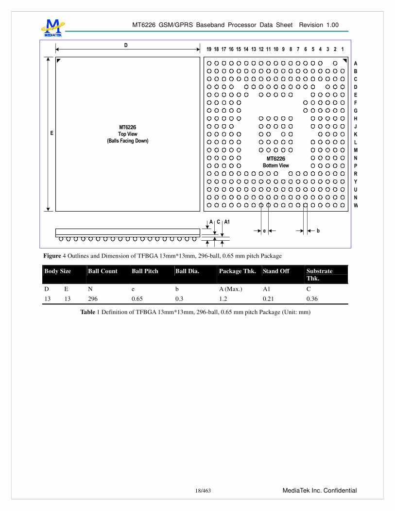
2.1 Pin Outs One type of package for this product, TFBGA 13mm*13mm, 296-ball, 0.65 mm pitch Package, is offered.
Pin outs and the top view are illustrated in Figure 3 for this package. Outline and dimension of package is illustrated in Figure 4, while the definition of package is shown in Table 1.

MT6226 GSM/GPRS Baseband Processor Data Sheet Revision 1.00
17/463 MediaTek Inc. Confidential
BBWAKEUP
AUXADIN6
SYSCLK
VSS33
AVDD_RTC AFCAVDD_
PLL
XIN
VSS33
AFC_BYP
AVSS_PLL
XOUT
TESTMODE
JTMS
AUX_REF
VDDK
JTCKJTDI
BPI_BUS1
JTRST#
BPI_BUS0 JTDOJRTCK
MT6226TFBGA
Top-View
B
A
C
E
D
F
G
H
J
K
L
M
N
P
14131211106321 87 954
GPIO7
DAIRST
DAIPCMIN
NC GPIO8GPIO9
GPIO4
DAISYNCGPIO6
VDDK
DAICLK
KROW1
KROW2
DAIPCMOUT
KROW3
KROW4
KCOL4
KCOL1KCOL2KCOL3
KCOL5KCOL6IRDA_PDN
IRDA_TXD
VDDK
URXD2
IRDA_RXDUTXD3URXD3 VSS33
UTXD1
UTXD2
URXD1
URTS1UCTS1
SIMDATA
ED6
ED7
EADV#
ECS5# ECS1#
EWR#
ED15
ECS2#
VSS33_EMI
VDD33_EMI
VSS33_EMI
ED8
ECS3# VDDK
ELB#
ED12 VDD33_EMI
VDD33_EMI
ECS0#
ED9
ECS4#
ERD#
VDDK
ED14
EUB# ED13
ED10
VSS33_EMI
EA6
EA3 VDD33_EMI ECS7#
EA10 EA7
EA4
EA0
ECS6#
EA11 EA8
VSS33_EMIEA12
VDD33_EMIEA9
EA2EA5
EA1
ECLK
SIMSEL
GPIO2 SIMCLKGPIO3
VDD33_MC
SIMRST
GPIO1MCINSMCWP
MCPWRON
MCCK
MCDA2
MCDA3
USB_DM
MCDA1
USB_DP
VDD33_USB
VSS33_EMI
WATCHDOG
EA25 EA24
EA22 EA13
EA21
EA18 EA15
MCDA0
VDD33_EMI
EA19
EA20
EA16
VSS33_EMI
VDD33_EMIEA17
EPDN#
1918171615
R
T
U
V
W
BPI_BUS6
BSI_CS0
LSCE0#
LRST#
NLD6
KROW0
VDD33
NLD0
MCCM0
ED11
VSS33_EMI
BPI_BUS2
BPI_BUS3
BPI_BUS4
BPI_BUS5
BPI_BUS7
BPI_BUS8VSS33 BPI_B
US9
BSI_DATA
BSI_CLK
LPCE1#VDD33 LSCE1
#
LPCE0#
LSCKLSDA
LRD#LPA0LWR#
NLD7NLD5VDDK
NLD4NLD2NLD1
NALENWE# NRNBNCLE
AU_OUT0_P
AVDD_AFE
AU_VIN0_P
AVSS_AFE
BDLAIP
AVDD_RFE
AUXADIN1
BUPAQN
AU_FMINR
AVDD_BUF
AU_MICBIAS
_N
AGND_AFE
AU_VIN1_P
AGND_RFE
AVSS_RFE
AUXADIN0
BUPAQP
AU_FMINL
AU_OUT0_N
AU_MICBIAS
_P
AU_VREF_P
AU_VIN1_N
BDLAQN
BUPAIN
APC
AUXADIN3
BDLAIN
AU_M_BYPL
BDLAQP
BUPAIP
AUXADIN2
AUXADIN5
AVSS_GSMRFTX
AVDD_GSMRFTX
AUXADIN4
AVSS_BUF
AU_VREF_N
AVSS_MBUF
AU_MOUTR
AU_MOUTL
AVDD_MBUF
AU_VIN0_N
IBOOT
LSA0
SIMVCC
NC
EA14 MFIQ
NRE#
NLD3
PWM1VDD33 MIRQ
SRCLKENA
ED5
SRCLKENAI
ALERTER
SYSRST#
SRCLKENA
N
VSS33_EMI
VDD33_EMI
EINT1
EINT0
GPIO0
ED3
EINT3
ED2
ED4
ED1 ED0
EA23
NCE#PWM2
EINT2
14131211106321 87 954 1918171615
B
A
C
E
D
F
G
H
J
K
L
M
N
P
R
T
U
V
W
GPIO5
NC
VSS33_MC
KCOL0 KROW5
VDD33
PLL_OUT
CMDAT9
CMDAT8
CMDAT7
CMDAT6
CMRST
CMPDN
CMDAT0
CMDAT1
CMHREF
CMVREF
CMMCLK
CMPCLK
CMDAT3
CMDAT2
CMDAT4
CMDAT5
NLD8 NLD9 NLD10
NLD11 NLD12
NLD13 NLD14 NLD15
NLD16
EWAIT
VSS33
VDD33_IS
AU_M_BYPR
AU_RBIAS
VDD33
VSS33_IS
VSS33_EMI
VSS33_IS
NC
NLD17
NC
NC
NC NC NC
NC
VDDK VSS33
Figure 3 Top View of MT6226 TFBGA 13mm*13mm, 296-ball, 0.65 mm pitch Package
MT6226 GSM/GPRS Baseband Processor Data Sheet Revision 1.00
18/463 MediaTek Inc. Confidential
26
T6226
!
"
#$ % & #' ( ) *####&#%
#
+
,
-
!
.
/
#$##*#)#(
Figure 4 Outlines and Dimension of TFBGA 13mm*13mm, 296-ball, 0.65 mm pitch Package
Body Size Ball Count Ball Pitch Ball Dia. Package Thk. Stand Off Substrate Thk.
D E N e b A (Max.) A1 C
13 13 296 0.65 0.3 1.2 0.21 0.36
Table 1 Definition of TFBGA 13mm*13mm, 296-ball, 0.65 mm pitch Package (Unit: mm)

MT6226 GSM/GPRS Baseband Processor Data Sheet Revision 1.00
19/463 MediaTek Inc. Confidential
2.2 Top Marking Definition
S
MT6226ADDDD-###LLLLL
MT6226A: Part No.DDDD: Date Code###: Subcontractor CodeLLLLL: Lot No.S: Special Code

MT6226 GSM/GPRS Baseband Processor Data Sheet Revision 1.00
20/463 MediaTek Inc. Confidential
2.3 DC Characteristics
2.3.1 Absolute Maximum Ratings Prolonged exposure to absolute maximum ratings may reduce device reliability. Functional operation at these maximum ratings is not implied.
Item Symbol Min Max Unit
IO power supply VDD33 -0.3 VDD33+0.3 V
I/O input voltage VDD33I -0.3 VDD33+0.3 V
Operating temperature Topr -20 80 Celsius
Storage temperature Tstg -55 125 Celsius

MT6226 GSM/GPRS Baseband Processor Data Sheet Revision 1.00
21/463 MediaTek Inc. Confidential
2.4 Pin Description Ball 13X13
Name Dir Description Mode0 Mode1 Mode2 Mode3
PU/PD
Reset
JTAG Port
E4 JTRST# I JTAG test port reset input PD Input E3 JTCK I JTAG test port clock input PU Input E2 JTDI I JTAG test port data input PU Input E1 JTMS I JTAG test port mode switch PU Input F5 JTDO O JTAG test port data output 0 F4 JRTCK O JTAG test port returned clock output 0
RF Parallel Control Unit
F3 BPI_BUS0 O RF hard-wire control bus 0 0 F2 BPI_BUS1 O RF hard-wire control bus 1 0 G5 BPI_BUS2 O RF hard-wire control bus 2 0 G4 BPI_BUS3 O RF hard-wire control bus 3 0 G3 BPI_BUS4 IO RF hard-wire control bus 4 0 G2 BPI_BUS5 IO RF hard-wire control bus 5 0 G1 BPI_BUS6 IO RF hard-wire control bus 6 GPIO10 BPI_BUS6 PD Input H5 BPI_BUS7 IO RF hard-wire control bus 7 GPIO11 BPI_BUS7 65MHz 26MHz PD Input H4 BPI_BUS8 IO RF hard-wire control bus 4 GPIO12 BPI_BUS8 13MHz 32KHz PD Input H3 BPI_BUS9 IO RF hard-wire control bus 5 GPIO13 BPI_BUS9 BSI_CS1 PD Input
RF Serial Control Unit
H1 BSI_CS0 O RF 3-wire interface chip select 0 0 J5 BSI_DATA O RF 3-wire interface data output 0 J4 BSI_CLK O RF 3-wire interface clock output 0
PWM Interface
R3 PWM1 IO Pulse width modulated signal 1 GPIO21 PWM1 DSP_GPO0
TBTXFS PD Input
R2 PWM2 IO Pulse width modulated signal 2 GPIO22 PWM2 DSP_GPO1
TBRXEN PD Input
T4 ALERTER IO Pulse width modulated signal for buzzer
GPIO23 ALERTER DSP_GPO2
BTRXFS PD Input
Serial LCD/PM IC Interface
J3 LSCK IO Serial display interface data output GPIO16 LSCK TDMA_CK
TBTXEN PU Input
J2 LSA0 IO Serial display interface address output GPIO17 LSA0 TDMA_D1 TDTIRQ PU Input J1 LSDA IO Serial display interface clock output GPIO18 LSDA TDMA_D0 TCTIRQ2 PU Input K4 LSCE0# IO Serial display interface chip select 0
output GPIO19 LSCE0# TDMA_FS TCTIRQ1 PU Input
K3 LSCE1# IO Serial display interface chip select 1 output
GPIO20 LSCE1# LPCE2# TEVTVAL
PU Input
Parallel LCD/Nand-Flash Interface
K2 LPCE1# IO Parallel display interface chip select 1 output
GPIO24 LPCE1# NCE1# MCU_TID0
PU Input
L5 LPCE0# O Parallel display interface chip select 0 output
1
L4 LRST# O Parallel display interface Reset Signal 1 L3 LRD# O Parallel display interface Read Strobe 1 L2 LPA0 O Parallel display interface address
output 1
L1 LWR# O Parallel display interface Write Strobe 1 F6 NLD17 IO Parallel LCD/Nand-Flash Data 17 GPIO56 NLD17 MCDA7 DSP_TID
0 PD Input

MT6226 GSM/GPRS Baseband Processor Data Sheet Revision 1.00
22/463 MediaTek Inc. Confidential
0 G6 NLD16 IO Parallel LCD/Nand-Flash Data 16 GPIO55 NLD16 MCDA6 PD Input L11 NLD15 IO Parallel LCD/Nand-Flash Data 15 PD Input L10 NLD14 IO Parallel LCD/Nand-Flash Data 14 PD Input L9 NLD13 IO Parallel LCD/Nand-Flash Data 13 PD Input K11 NLD12 IO Parallel LCD/Nand-Flash Data 12 PD Input K9 NLD11 IO Parallel LCD/Nand-Flash Data 11 PD Input J11 NLD10 IO Parallel LCD/Nand-Flash Data 10 PD Input J10 NLD9 IO Parallel LCD/Nand-Flash Data 9 PD Input J9 NLD8 IO Parallel LCD/Nand-Flash Data 8 PD Input M5 NLD7 IO Parallel LCD/Nand-Flash Data 7 PD Input M4 NLD6 IO Parallel LCD/Nand-Flash Data 6 PD Input M3 NLD5 IO Parallel LCD/Nand-Flash Data 5 PD Input N5 NLD4 IO Parallel LCD/Nand-Flash Data 4 PD Input N4 NLD3 IO Parallel LCD/Nand-Flash Data 3 PD Input N3 NLD2 IO Parallel LCD/Nand-Flash Data 2 PD Input N2 NLD1 IO Parallel LCD/Nand-Flash Data 1 PD Input N1 NLD0 IO Parallel LCD/Nand-Flash Data 0 PD Input P5 NRNB IO Nand-Flash Read/Busy Flag GPIO25 NRNB DSP_TID1 MCU_TID
1 PU Input
P4 NCLE IO Nand-Flash Command Latch Signal GPIO26 NCLE DSP_TID2 MCU_TID2
PD Input
P3 NALE IO Nand-Flash Address Latch Signal GPIO27 NALE DSP_TID3 MCU_TID3
PD Input
P2 NWE# IO Nand-Flash Write Strobe GPIO28 NWE# DSP_TID4 MCU_DID
PU Input
P1 NRE# IO Nand-Flash Read Strobe GPIO29 NRE# DSP_TID5 MCU_DFS
PU Input
R4 NCE# IO Nand-Flash Chip select output GPIO30 NCE# DSP_TID6 MCU_DCK
PU Input
SIM Card Interface
L18 SIMRST O SIM card reset output 0 L17 SIMCLK O SIM card clock output 0 K15 SIMVCC O SIM card supply power control 0 K16 SIMSEL O SIM card supply power select GPIO32 SIMSEL PD Input K17 SIMDATA IO SIM card data input/output 0
Dedicated GPIO Interface
U2 GPIO0 IO General purpose input/output 0 GPIO0 DICK DSP_GPO3
PD Input
M19 GPIO1 IO General purpose input/output 1 GPIO1 BSI_RFIN PD Input L15 GPIO2 IO General purpose input/output 2 GPIO2 DID PD Input L16 GPIO3 IO General purpose input/output 3 GPIO3 DIMS PD Input C17 GPIO4 IO General purpose input/output 4 GPIO4 DSP_CLK DSPLCK EDICK PD Input A19 GPIO5 IO General purpose input/output 5 GPIO5 AHB_CLK DSPLD3 EDIWS PD Input B18 GPIO6 IO General purpose input/output 6 GPIO6 ARM_CL
K DSPLD2 CMFLAS
H PD Input
B17 GPIO7 IO General purpose input/output 7 GPIO7 SLOW_CK DSPLD1 EDIDAT PD Input A18 GPIO8 IO General purpose input/output 19 GPIO8 SCL DSPLD0 PD Input A17 GPIO9 IO General purpose input/output 21 GPIO9 SDA DSPLSYN
C PD Input
Miscellaneous
U1 SYSRST# I System reset input active low Input R18 WATCHDO
G# O Watchdog reset output 1

MT6226 GSM/GPRS Baseband Processor Data Sheet Revision 1.00
23/463 MediaTek Inc. Confidential
T3 SRCLKENAN
O External TCXO enable output active low
GPO1 SRCLKENAN
0
T1 SRCLKENA O External TCXO enable output active high
GPO0 SRCLKENA
1
T2 SRCLKENAI IO External TCXO enable input GPIO31 SRCLKENAI
PD Input
E5 IBOOT I Boot Device Configuration Input PD Input
Keypad Interface
G17 KCOL6 I Keypad column 6 PU Input G18 KCOL5 I Keypad column 5 PU Input G19 KCOL4 I Keypad column 4 PU Input F15 KCOL3 I Keypad column 3 PU Input F16 KCOL2 I Keypad column 2 PU Input F17 KCOL1 I Keypad column 1 PU Input F18 KCOL0 I Keypad column 0 PU Input F19 KROW5 O Keypad row 5 0 E16 KROW4 O Keypad row 4 0 E17 KROW3 O Keypad row 3 0 E18 KROW2 O Keypad row 2 0 D16 KROW1 O Keypad row 1 0 D19 KROW0 O Keypad row 0 0
External Interrupt Interface
V1 EINT0 I External interrupt 0 PU Input U3 EINT1 I External interrupt 1 PU Input W1 EINT2 I External interrupt 2 PU Input V2 EINT3 I External interrupt 3 PU Input R5 MIRQ I Interrupt to MCU GPIO41 MIRQ 13MHz 32KHz PU Input R17 MFIQ I Interrupt to MCU GPIO42 MFIQ PU Input
External Memory Interface
R16 ED0 IO External memory data bus 0 Input R15 ED1 IO External memory data bus 1 Input T19 ED2 IO External memory data bus 2 Input T17 ED3 IO External memory data bus 3 Input U19 ED4 IO External memory data bus 4 Input U18 ED5 IO External memory data bus 5 Input V18 ED6 IO External memory data bus 6 Input W19 ED7 IO External memory data bus 7 Input U17 ED8 IO External memory data bus 8 Input V17 ED9 IO External memory data bus 9 Input W17 ED10 IO External memory data bus 10 Input T16 ED11 IO External memory data bus 11 Input W16 ED12 IO External memory data bus 12 Input T15 ED13 IO External memory data bus 13 Input U15 ED14 IO External memory data bus 14 Input V15 ED15 IO External memory data bus 15 Input U14 ERD# O External memory read strobe 1 W14 EWR# O External memory write strobe 1 R13 ECS0# O External memory chip select 0 1 T13 ECS1# O External memory chip select 1 1 U13 ECS2# O External memory chip select 2 1 V13 ECS3# O External memory chip select 3 1 R12 ECS4# O External memory chip select 4 GPIO54 ECS4# PU 1 T12 ECS5# O External memory chip select 5 GPIO53 ECS5# PU 1

MT6226 GSM/GPRS Baseband Processor Data Sheet Revision 1.00
24/463 MediaTek Inc. Confidential
U12 ECS6# O External memory chip select 6 GPIO52 ECS6# PU 1 W12 ECS7# O External memory chip select 7 GPIO40 ECS7# PU 1 R14 ELB# O External memory lower byte strobe 1 T14 EUB# O External memory upper byte strobe 1 T11 EPDN# O Power Down Control Signal for
PSRAM GPO2 EPDN# 6.5MHz 26MHz 0
U11 EADV# O Address valid for burst mode flash memory
1
R11 EWAIT O External device wait signal Input V11 ECLK O Clock for flash memory 0 R10 EA0 O External memory address bus 0 0 T10 EA1 O External memory address bus 1 0 U10 EA2 O External memory address bus 2 0 W10 EA3 O External memory address bus 3 0 T9 EA4 O External memory address bus 4 0 U9 EA5 O External memory address bus 5 0 V9 EA6 O External memory address bus 6 0 R8 EA7 O External memory address bus 7 0 T8 EA8 O External memory address bus 8 0 W8 EA9 O External memory address bus 9 0 R7 EA10 O External memory address bus 10 0 T7 EA11 O External memory address bus 11 0 U7 EA12 O External memory address bus 12 0 V7 EA13 O External memory address bus 13 0 R6 EA14 O External memory address bus 14 0 T6 EA15 O External memory address bus 15 0 U6 EA16 O External memory address bus 16 0 W6 EA17 O External memory address bus 17 0 T5 EA18 O External memory address bus 18 0 U5 EA19 O External memory address bus 19 0 V5 EA20 O External memory address bus 20 0 W5 EA21 O External memory address bus 21 0 V4 EA22 O External memory address bus 22 0 U4 EA23 O External memory address bus 23 0 W3 EA24 O External memory address bus 24 GPO3 EA24 0 W2 EA25 O External memory address bus 25 GPO4 EA25 13MHz 32KHz 0
USB Interface
P16 USB_DP IO USB D+ Input/Output P17 USB_DM IO USB D- Input/Output
Memory Card Interface
P19 MCCM0 IO SD Command/MS Bus State Output N15 MCDA0 IO SD Serial Data IO 0/MS Serial Data
IO
N16 MCDA1 IO SD Serial Data IO 1 N17 MCDA2 IO SD Serial Data IO 2 N18 MCDA3 IO SD Serial Data IO 3 N19 MCCK O SD Serial Clock/MS Serial Clock
Output
M16 MCPWRON O SD Power On Control Output M17 MCWP I SD Write Protect Input GPIO15 MCWP PU M18 MCINS I SD Card Detect Input GPIO14 MCINS PU
UART Interface
K18 URXD1 I UART 1 receive data PU Input

MT6226 GSM/GPRS Baseband Processor Data Sheet Revision 1.00
25/463 MediaTek Inc. Confidential
K19 UTXD1 O UART 1 transmit data 1 J16 UCTS1 I UART 1 clear to send PU Input J17 URTS1 O UART 1 request to send 1 J18 URXD2 IO UART 2 receive data GPIO35 URXD2 UCTS3 EINT6 PU Input J19 UTXD2 IO UART 2 transmit data GPIO36 UTXD2 URTS3 EINT4 PU Input H15 URXD3 IO UART 3 receive data GPIO33 URXD3 EINT7 PU Input H16 UTXD3 IO UART 3 transmit data GPIO34 UTXD3 EINT5 PU Input H17 IRDA_RXD IO IrDA receive data GPIO37 IRDA_RX
D UCTS2 PU Input
G15 IRDA_TXD IO IrDA transmit data GPIO38 IRDA_TXD
URTS2 PU Input
G16 IRDA_PDN IO IrDA Power Down Control GPIO39 IRDA_PDN
PU Input
Digital Audio Interface
D17 DAICLK IO DAI clock output GPIO43 DAICLK DSPLD7 PU Input D18 DAIPCMOUT IO DAI pcm data out GPIO44 DAIPCMO
UT DSPLD6 PD Input
C19 DAIPCMIN IO DAI pcm data input GPIO45 DAIPCMIN
DSPLD5 PU Input
C18 DAIRST IO DAI reset signal input GPIO47 DAIRST DSPLD4 PU Input B19 DAISYNC IO DAI frame synchronization signal
output GPIO46 DAISYNC BFEPRBO PU Input
Image Sensor Interface
J12 CMRST IO Image sensor reset signal output GPIO48 CMRST PD Input K12 CMPDN IO Image sensor power down control GPIO49 CMPDN PD Input H12 CMVREF I Sensor vertical reference signal input Input H11 CMHREF I Sensor horizontal reference signal
input Input
H9 CMPCLK I Image sensor pixel clock input Input H10 CMMCLK O Image sensor master clock output Outp
ut H8 CMDAT9 I Image sensor data input 9 Input J8 CMDAT8 I Image sensor data input 8 Input K8 CMDAT7 I Image sensor data input 7 Input L8 CMDAT6 I Image sensor data input 6 Input M8 CMDAT5 I Image sensor data input 5 Input M9 CMDAT4 I Image sensor data input 4 Input M10 CMDAT3 I Image sensor data input 3 Input M11 CMDAT2 I Image sensor data input 2 Input M12 CMDAT1 IO Image sensor data input 1 GPIO50 CMDAT1 MCDA5 PD Input L12 CMDAT0 IO Image sensor data input 0 GPIO51 CMDAT0 MCDA4 PD Input
Analog Interface
B15 AU_MOUL Audio analog output left channel A15 AU_MOUR Audio analog output right channel C14 AU_M_BYP
L Audio DAC bypass pin
B14 AU_FMINL FM radio analog input left channel A14 AU_FMINR FM radio analog input right channel D13 AU_R_BIAS Audio DAC bias resistor pin C13 AU_M_BYP
R Audio DAC bypass pin
B12 AU_OUT0_N Earphone 0 amplifier output (-) A12 AU_OUT0_P Earphone 0 amplifier output (+) C12 AU_MICBIA
S_P Microphone bias supply (+)

MT6226 GSM/GPRS Baseband Processor Data Sheet Revision 1.00
26/463 MediaTek Inc. Confidential
D12 AU_MICBIAS_N
Microphone bias supply (-)
C11 AU_VREF_N Audio reference voltage (-) B11 AU_VREF_P Audio reference voltage (+) D10 AU_VIN0_P Microphone 0 amplifier input (+) C10 AU_VIN0_N Microphone 0 amplifier input (-) B10 AU_VIN1_N Microphone 1 amplifier input (-) A10 AU_VIN1_P Microphone 1 amplifier input (+) D9 BDLAQP Quadrature input (Q+) baseband codec
downlink
C9 BDLAQN Quadrature input (Q-) baseband codec downlink
A9 BDLAIN In-phase input (I+) baseband codec downlink
B9 BDLAIP In-phase input (I-) baseband codec downlink
B8 BUPAIP In-phase output (I+) baseband codec uplink
A8 BUPAIN In-phase output (I-) baseband codec uplink
C8 BUPAQN Quadrature output (Q+) baseband codec uplink
D8 BUPAQP Quadrature output (Q-) baseband codec uplink
B7 APC Automatic power control DAC output D6 AUXADIN0 Auxiliary ADC input 0 C6 AUXADIN1 Auxiliary ADC input 1 B6 AUXADIN2 Auxiliary ADC input 2 A6 AUXADIN3 Auxiliary ADC input 3 C5 AUXADIN4 Auxiliary ADC input 4 B5 AUXADIN5 Auxiliary ADC input 5 A5 AUXADIN6 Auxiliary ADC input 6 C4 AUX_REF Auxiliary ADC reference voltage input B4 AFC Automatic frequency control DAC
output
A4 AFC_BYP Automatic frequency control DAC bypass capacitance
VCXO Interface
A2 SYSCLK 13MHz or 26MHz system clock input D5 PLL_OUT PLL test pin
RTC Interface
C2 XIN 32.768 KHz crystal input B1 XOUT 32.768 KHz crystal output C1 BBWAKEUP O Baseband power on/off control 1 D3 TESTMODE I TESTMODE enable input PD Input
Supply Voltages
D1 VDDK Supply voltage of internal logic M1 VDDK Supply voltage of internal logic V8 VDDK Supply voltage of internal logic E11 VDDK Supply voltage of internal logic V16 VDDK Supply voltage of internal logic H19 VDDK Supply voltage of internal logic C16 VDDK Supply voltage of internal logic W4 VDD33_EMI Supply voltage of memory interface
driver

MT6226 GSM/GPRS Baseband Processor Data Sheet Revision 1.00
27/463 MediaTek Inc. Confidential
W7 VDD33_EMI Supply voltage of memory interface driver
W9 VDD33_EMI Supply voltage of memory interface driver
W11 VDD33_EMI Supply voltage of memory interface driver
W13 VDD33_EMI Supply voltage of memory interface driver
W15 VDD33_EMI Supply voltage of memory interface driver
W18 VDD33_EMI Supply voltage of memory interface driver
T18 VDD33_EMI Supply voltage of memory interface driver
V3 VSS33_EMI Ground of memory interface driver V6 VSS33_EMI Ground of memory interface driver U8 VSS33_EMI Ground of memory interface driver V10 VSS33_EMI Ground of memory interface driver V12 VSS33_EMI Ground of memory interface driver V14 VSS33_EMI Ground of memory interface driver U16 VSS33_EMI Ground of memory interface driver V19 VSS33_EMI Ground of memory interface driver R19 VSS33_EMI Ground of memory interface driver P15 VDD33_USB Supply voltage of USB transceiver M15 VDD33_MC Supply voltage of memory card
interface drivers
P18 VSS33_USB/MC
Ground of USB/memory card interface
E15 VDD33_IS Supply voltage of image sensor interface drivers
A16 VSS33_IS Ground of image sensor interface E14 VSS33_IS Ground of image sensor interface F1 VDD33 Supply voltage for pad K1 VDD33 Supply voltage for pad R1 VDD33 Supply voltage for pad L19 VDD33 Supply voltage for pad E19 VDD33 Supply voltage for pad D2 VSS33 Ground H2 VSS33 Ground M2 VSS33 Ground H18 VSS33 Ground B16 VSS33 Ground E12 VSS33 Ground B2 AVDD_RTC Supply voltage for Real Time Clock
Analog Supplies
B3 AVDD_PLL Supply voltage for PLL C3 AVSS_PLL Ground for PLL supply C15 AVDD_MBU
F Supply Voltage for Audio band section
D14 AVSS_MBUF GND for Audio band section B13 AVDD_BUF Supply voltage for voice band transmit
section
A13 AVSS_BUF GND for voice band transmit section D11 AVDD_AFE Supply voltage for voice band receive
section

MT6226 GSM/GPRS Baseband Processor Data Sheet Revision 1.00
28/463 MediaTek Inc. Confidential
A11 AGND_AFE GND reference voltage for voice band section
E10 AVSS_AFE GND for voice band receive section E9 AGND_RFE GND reference voltage for baseband
section, APC, AFC and AUXADC
E8 AVSS_GSMRFTX
GND for baseband transmit section
D7 AVDD_GSMRFTX
Supply voltage for baseband transmit section
C7 AVSS_RFE GND for baseband receive section, APC, AFC and AUXADC
A7 AVDD_RFE Supply voltage for baseband receive section, APC, AFC and AUXADC
Table 2 Pin Descriptions (Bolded types are functions at reset)

MT6226 GSM/GPRS Baseband Processor Data Sheet Revision 1.00
29/463 MediaTek Inc. Confidential
2.5 Power Description Ball 13X13
Name IO Supply IO GND Core Supply Core GND Remark
A19 GPIO5 A18 GPIO6 B17 GPIO7 A18 GPIO8 A17 GPIO9
VDD33 VSS33 VDDK VSSK
B16 VSS33 C16 VDDK Typ. 1.8V A16 VSS33_IS J12 CMRST K12 CMPDN H12 CMVREF H11 CMHREF H9 CMPCLK H10 CMMCLK H8 CMDAT9
VDD33_IS VSS33_IS VDDK VSSK
E15 VDD33_IS Typ. 1.8~2.8V J8 CMDAT8 K8 CMDAT7 L8 CMDAT6 M8 CMDAT5 M9 CMDAT4 M10 CMDAT3 M11 CMDAT2 M12 CMDAT1 L12 CMDAT0
VDD33_IS VSS33_IS VDDK VSSK
E12 VSS33 E11 VDDK Typ. 1.8V E14 VSS33_IS C15 AVDD_MBUF Typ. 2.8V B15 AU_MOUTL A15 AU_MOUTR D14 AVSS_MBUF C14 AU_M_BYPL C13 AU_M_BYPR D13 AU_R_BIAS B14 AU_FMINL A14 AU_FMINR B12 AU_OUT0_N B13 AVDD_BUF Typ. 2.8V A12 AU_OUT0_P A13 AVSS_BUF C12 AU_MICBIAS_P D12 AU_MICBIAS_N D11 AVDD_AFE Typ. 2.8V C11 AU_VREF_N B11 AU_VREF_P A11 AGND_AFE D10 AU_VIN0_P

MT6226 GSM/GPRS Baseband Processor Data Sheet Revision 1.00
30/463 MediaTek Inc. Confidential
C10 AU_VIN0_N B10 AU_VIN1_N A10 AU_VIN1_P E10 AVSS_AFE D9 BDLAQP C9 BDLAQN E9 AGND_RFE A9 BDLAIN B9 BDLAIP E8 AVSS_GSMRFTX B8 BUPAIP A8 BUPAIN D7 AVDD_GSMRFTX Typ. 2.8V C8 BUPAQN D8 BUPAQP C7 AVSS_RFE B7 APC A7 AVDD_RFE Typ. 2.8V D6 AUXADIN0 C6 AUXADIN1 B6 AUXADIN2 A6 AUXADIN3 C5 AUXADIN4 B5 AUXADIN5 A5 AUXADIN6 C4 AUX_REF B4 AFC A4 AFC_BYP B3 AVDD_PLL Typ. 2.8V D5 PLL_OUT A2 SYSCLK
AVDD_PLL AVSS_PLL AVDD_PLL AVSS_PLL
C3 AVSS_PLL B2 AVDD_RTC Typ. 1.8V B1 XOUT C2 XIN C1 BBWAKEUP D3 TESTMODE
AVDD_RTC VSS33 AVDD_RTC VSS33
D2 VSS33 D1 VDDK Typ. 1.8V E5 IBOOT E4 JTRST# E3 JTCK E2 JTDI E1 JTMS F5 JTDO F4 JRTCK F3 BPI_BUS0 F2 BPI_BUS1 F6 NLD17
VDD33 VSS33 VDDK VSSK
F1 VDD33 Typ. 2.8V G6 NLD16 G5 BPI_BUS2 G4 BPI_BUS3
VDD33
VSS33 VDDK VSSK

MT6226 GSM/GPRS Baseband Processor Data Sheet Revision 1.00
31/463 MediaTek Inc. Confidential
G3 BPI_BUS4 G2 BPI_BUS5 G1 BPI_BUS6 H5 BPI_BUS7 H4 BPI_BUS8 H3 BPI_BUS9 H1 BSI_CS0
H2 VSS33 J5 BSI_DATA J4 BSI_CLK J3 LSCK J2 LSA0 J1 LSDA K4 LSCE0# K3 LSCE1# K2 LPCE1# L11 NLD15 L10 NLD14 L9 NLD13
VDD33 VSS33
VDDK VSSK
K1 VDD33 Typ. 2.8V L5 LPCE0# L4 LRST# L3 LRD# L2 LPA0 L1 LWR# K11 NLD12 K9 NLD11 J11 NLD10 J10 NLD9 J9 NLD8 M5 NLD7
VDD33 VSS33 VDDK VSSK
M2 VSS33 M1 VDDK Typ. 1.8V M4 NLD6 M3 NLD5 N5 NLD4 N4 NLD3 N3 NLD2 N2 NLD1 N1 NLD0 P5 NRNB P4 NCLE P3 NALE
VDD33 VSS33 VDDK VSSK
R1 VDD33 Typ. 2.8V P2 NWE# VDDK VSSK P1 NRE# R4 NCE# R3 PWM1
R2 PWM2
T4 ALERTER
T1 SRCLKENA
T3 SRCLKENAN
VDD33 VSS33

MT6226 GSM/GPRS Baseband Processor Data Sheet Revision 1.00
32/463 MediaTek Inc. Confidential
T2 SRCLKENAI
U1 SYSRST#
U2 GPIO0
V1 EINT0
U3 EINT1
W1 EINT2
V2 EINT3
V3 VSS33_EMI
W2 EA25 W3 EA24 U4 EA23 V4 EA22
VDD33_EMI
VSS33_EMI
VDDK VSSK
W4 VDD33_EMI Typ. 1.8~2.8V R5 MIRQ W5 EA21 V5 EA20 U5 EA19 T5 EA18
VDD33_EMI
VSS33_EMI
VDDK VSSK
V6 VSS33_EMI W6 EA17 U6 EA16 T6 EA15 R6 EA14
VDD33_EMI
VSS33_EMI
VDDK VSSK
W7 VDD33_EMI Typ. 1.8~2.8V V7 EA13 U7 EA12 T7 EA11 R7 EA10
VDD33_EMI VSS33_EMI VDDK VSSK
V8 VDDK Typ. 1.8V U8 VSS33_EMI W8 EA9 T8 EA8 R8 EA7 V9 EA6
VDD33_EMI
VSS33_EMI
VDDK VSSK
W9 VDD33_EMI Typ. 1.8~2.8V U9 EA5 T9 EA4 W10 EA3
VDD33_EMI
VSS33_EMI
VDDK VSSK
V10 VSS33_EMI U10 EA2 T10 EA1 R10 EA0
VDD33_EMI VSS33_EMI VDDK VSSK
W11 VDD33_EMI Typ. 1.8~2.8V R11 EWAIT U11 EADV# V11 ECLK T11 EPDN#
VDD33_EMI VSS33_EMI VDDK VSSK
V12 VSS33_EMI W12 ECS7# U12 ECS6# T12 ECS5# R12 ECS4#
VDD33_EMI VSS33_EMI VDDK VSSK

MT6226 GSM/GPRS Baseband Processor Data Sheet Revision 1.00
33/463 MediaTek Inc. Confidential
W13 VDD33_EMI Typ. 1.8~2.8V V13 ECS3# U13 ECS2# T13 ECS1# R13 ECS0#
VDD33_EMI
VSS33_EMI
VDDK VSSK
V14 VSS33_EMI W14 EWR# U14 ERD# T14 EUB# R14 ELB#
VDD33_EMI
VSS33_EMI
VDDK VSSK
W15 VDD33_EMI Typ. 1.8~2.8V V15 ED15 U15 ED14 T15 ED13 W16 ED12
VDD33_EMI VSS33_EMI VDDK VSSK
V16 VDDK 1.8V
U16 VSS33_EMI
T16 ED11 W17 ED10 V17 ED9
VDD33_EMI VSS33_EMI VDDK VSSK
W18 VDD33_EMI Typ. 1.8~2.8V U17 ED8 W19 ED7 V18 ED6
VDD33_EMI VSS33_EMI VDDK VSSK
V19 VSS33_EMI U18 ED5 U19 ED4 T17 ED3
VDD33_EMI VSS33_EMI VDDK VSSK
T18 VDD33_EMI Typ. 1.8~2.8V T19 ED2 R15 ED1 R16 ED0 R17 MFIQ R18 WATCHDOG
VDD33_EMI
VSS33_EMI
VDDK VSSK
R19 VSS33_EMI P15 VDD33_USB Typ. 3.3V P16 USB_DP P17 USB_DM
VDD33_USB VSS33_USB/MC
VDDK VSSK
P18 VSS33_USB/MC P19 MCCM0 N15 MCDA0 N16 MCDA1 N17 MCDA2 N18 MCDA3 N19 MCCK M16 MCPWRON M17 MCWP M18 MCINS
VDD33_MC
VSS33_USB/MC
VDDK VSSK
M15 VDD33_MC Typ. 2.8V L19 VDD33 Typ. 2.8V M19 GPIO1 L15 GPIO2
VDD33 VSS33 VDDK VSSK

MT6226 GSM/GPRS Baseband Processor Data Sheet Revision 1.00
34/463 MediaTek Inc. Confidential
L16 GPIO3 L18 SIMRST L17 SIMCLK K15 SIMVCC K16 SIMSEL K17 SIMDATA K18 URXD1 K19 UTXD1 J16 UCTS1 J17 URTS1 J18 URXD2 J19 UTXD2
H19 VDDK Typ. 1.8V H18 VSS33 H15 URXD3 H16 UTXD3 H17 IRDA_PDN G15 IRDA_TXD G16 IRDA_RXD G17 KCOL6 G18 KCOL5 G19 KCOL4 F15 KCOL3 F16 KCOL2 F17 KCOL1 F18 KCOL0 F19 KROW5
VDD33
VSS33
VDDK VSSK
E19 VDD33 Typ. 2.8V E16 KROW4 E17 KROW3 E18 KROW2 D16 KROW1 D19 KROW0 D17 DAICLK D18 DAIPCMOUT C19 DAIPCMIN C18 DAIRST B19 DAISYNC C17 GPIO4
VDD33 VSS33 VDDK VSSK
Table 3 Power Descriptions

MT6226 GSM/GPRS Baseband Processor Data Sheet Revision 1.00
35/463 MediaTek Inc. Confidential
3 Micro-Controller Unit Subsystem
Figure 5 illustrates the block diagram of the Micro-Controller Unit Subsystem in MT6226. The subsystem utilizes a main 32-bit ARM7EJ-S RISC processor, which plays the role of the main bus master controlling the whole subsystem. The processor communicates with all the other on-chip modules via the two-level system buses: AHB Bus and APB Bus. All bus transactions originate from bus masters, while slaves can only respond to requests from bus masters. Before data transfer can be established, bus master must ask for bus ownership. This is accomplished by request-grant handshaking protocol between masters and arbiters.
Two levels of bus hierarchy are designed to provide optimum usage for different performance requirements. Specifically, AHB Bus, the main system bus, is tailored toward high-speed requirements and provides 32-bit data path with multiplex scheme for bus interconnections. The APB bus, on the other hand, is designed to reduce interface complexity for lower data transfer rate, and so it is isolated from high bandwidth AHB Bus by APB Bridge. It supports 16-bit addressing and both 16-bit and 32-bit data paths. APB Bus is also optimized for minimal power consumption by employing gated-clock scheme.
During operation, if the target slave is located on the AHB Bus, the transaction is conducted directly on AHB Bus. However, if the target slave is a peripheral and is attached to the APB bus, then the transaction is conducted between AHB and APB bus through the use of APB Bridge.
The MT6226 MCU subsystem supports only memory addressing method, therefore all components are mapped onto MCU 32-bit address space. A Memory Management Unit is employed to allow for a central decode scheme. It generates appropriate selection signals for each memory-addressed modules on the AHB Bus.
In order to off-load the processor core, a DMA Controller is designated to act as a master and share the bus resources on AHB Bus to perform fast data movement between modules. This controller provides fourteen DMA channels.
The Interrupt Controller provides a software interface to manipulate interrupt events. It can handle up to 32 interrupt sources asserted at the same time. In general, it generates 2 levels of interrupt requests, FIQ and IRQ, to the processor.
A 512K Byte SRAM is provided as system memory for high-speed data access. For factory programming purposes, a Boot ROM module is also integrated. These two modules use the same Internal Memory Controller to connect to AHB Bus.
External Memory Interface supports both 8-bit and 16-bit devices. Since AHB Bus is 32-bit wide, all the data transfer will be converted into several 8-bit or 16-bit cycles depending on the data width of the target device. Note that, this interface supports both synchronous and asynchronous components, such as Flash, SRAM and parallel LCD. This interface supports also page and burst mode type of Flash.

MT6226 GSM/GPRS Baseband Processor Data Sheet Revision 1.00
36/463 MediaTek Inc. Confidential
MCU-DSPInterface
ARM7EJ-S
ExternalMemoryInterface
System RAM
DMAController
APBBridge
System ROM
PeripheralPeripheral
InterruptController
Internal MemoryController Arbiter
AHB Bus
APB Bus
ExtBus
USB
Figure 5 Block Diagram of the Micro-Controller Unit Subsystem in MT6226
3.1 Processor Core
3.1.1 General Description The Micro-Controller Unit Subsystem in MT6226 uses the 32-bit ARM7EJ-S RISC processor that is based on the Von Neumann architecture with a single 32-bit data bus carrying both instructions and data. The memory interface of ARM7EJ-S is totally compliant to AMBA based bus system, which allows direct connection to the AHB Bus.
3.2 Memory Management The processor core of MT6226 supports only memory addressing method for instruction fetch and data access. It manages a 32-bit address space that has addressing capability up to 4GB. System RAM, System ROM, Registers, MCU Peripherals and external components are all mapped onto such 32-bit address space, as depicted in Figure 10.

MT6226 GSM/GPRS Baseband Processor Data Sheet Revision 1.00
37/463 MediaTek Inc. Confidential
MCU 32-bitAddressing
Space
EA[25:0]Addressing
Space
APB Peripherals
MCU-DSP Interface
Reserved
8FFF_FFFFh|
8000_0000h
7FFF_FFFFh|
7000_0000h
6FFF_FFFFh|
5000_0000h
4FFF_FFFFh|
4000_0000h
3FFF_FFFFh|
0000_0000hExternal Memroy
Internal Memory
7800_0000h
7000_0000h USB
Virtual FIFO
9FFF_FFFh|
9000_0000h
9800_0000h
9000_0000h LCD
Reserved
Figure 10 The Memory Layout of MT6226
The address space is organized into blocks with size of 256M Bytes each. Memory blocks 0-97FFFFFFh are defined and currently dedicated to specific functions, while the others are reserved for future usage. The block number is uniquely selected by address line A31-A28 of the internal system bus.
3.2.1.1 External Access
To allow external access, the MT6226 outputs 26 bits (A25-A0) of address lines along with 8 selection signals that correspond to associated memory blocks. That is, MT6226 can support up to 8 MCU addressable external components. The data width of internal system bus is fixed at 32-bit wide, while the data width of the external components can be either 8 or 16 bit.
Since devices are usually available with varied operating grades, adaptive configurations for different applications are needed. MT6226 provides software programmable registers to configure their wait-states to adapt to different operating conditions.
3.2.1.2 Memory Re-mapping Mechanism
To permit more flexible system configuration, a memory re-mapping mechanism is provided. It allows software program to swap BANK0 (ECS0#) and BANK1 (ECS1#) dynamically. Whenever the bit value of RM0 in register

MT6226 GSM/GPRS Baseband Processor Data Sheet Revision 1.00
38/463 MediaTek Inc. Confidential
EMI_REMAP is changed, these two banks will be swapped accordingly. Furthermore, it allows system to boot in different sequences as detailed in 3.2.1.3 Boot Sequence.
3.2.1.3 Boot Sequence
Since the ARM7EJ-S core always starts to fetch instructions from the lowest memory address at 00000000h after system has been reset, it is designed to have a dynamic mapping architecture capable of associating Boot Code, external Flash or external SRAM with the memory block 0000_0000h – 07ff_ffffh.
By default, the Boot Code is mapped onto 0000_0000h – 07ff_ffffh while the state of IBOOT is “0”. But, this configuration can be changed by altering the state of IBOOT before system reset, or by programming bit value of RM1 in register EMI_REMAP directly.
MT6226 system provides two kinds of boot up scheme:
Start up system of running codes from Boot Code for factory programming
Start up system of running codes from external FLASH or ROM device for normal operation
Boot Code
The Boot Code is placed together with Memory Re-Mapping Mechanism in External Memory Controller and comprises of just two words of instructions as shown below. There is a jump instruction that leads the processor to run the code starting at address of 48000000h where the System ROM is placed.
ADDRESS BINARY CODE ASSEMBLY
00000000h E51FF004h LDR PC, 0x4
00000004h 48000000h (DATA)
Factory Programming
The configuration for factory programming is shown in Figure 11. Usually the Factory Programming Host connects with MT6226 via the UART interface. In order to have it work properly, the system should boot up from Boot Code. That is, IBOOT should be tied to GND. The download speed can be up to 921K bps while MCU is running at 26MHz.
After the system has reset, the Boot Code will guide the processor to run the Factory Programming software placed in System ROM. Then, MT6226 will start and continue to poll the UART1 port until valid information is detected. The first information received on the UART1 will be used to configure the chip for factory programming. The Flash downloader program is then transferred into System RAM or external SRAM.
Further information will be detailed in MT6226 Software Programming Specification.
BaseBand ProcessorFactory
ProgrammingHost
FLASH
UART
ExternalMemoryInterface
IBOOT
Figure 11 System configuration required for factory programming

MT6226 GSM/GPRS Baseband Processor Data Sheet Revision 1.00
39/463 MediaTek Inc. Confidential
3.2.1.4 Little Endian Mode
The MT6226 system always treats 32-bit words of memory in Little Endian format. In Little Endian mode, the lowest numbered byte in a word is stored in the least significant position, and the highest numbered byte in the most significant position. Byte 0 of the memory system is therefore connected to data lines 7 through 0.
3.3 Bus System
3.3.1 General Description Two levels of bus hierarchy are employed in the Micro-Controller Unit Subsystem of MT6226. As depicted in Figure 5, AHB Bus and APB Bus serve as system backbone and peripheral buses, while an APB bridge connects these two buses. Both AHB and APB Buses operate at the same clock rate as processor core.
The APB Bridge is the only bus master residing on the APB bus. All APB slaves are mapped onto memory block MB8 in MCU 32-bit addressing space. A central address decoder is implemented inside the bridge to generate select signals for individual peripherals. In addition, since the base address of each APB slave has been associated with select signals, the address bus on APB will contains only the value of offset address.
The maximum address space that can be allocated to a single APB slave is 64KB, i.e. 16-bit address lines. The width of the data bus is mainly constrained to 16-bit in order to minimize the design complexity and power consumption while some uses 32-bit data bus to accommodate more bandwidth. In the case where an APB slave needs large amount of transfers, the device driver can also request DMA channels to conduct a burst of data transfer. The base address and data width of each peripheral are listed in Table 6.
Base Address Description Data
Width Software Base ID
8000_0000h Configuration Registers (Clock, Power Down, Version and Reset)
16 CONFG Base
8001_0000h External Memory Interface 32 EMI Base
8002_0000h Interrupt Controller 32 CIRQ Base
8003_0000h DMA Controller 32 DMA Base
8004_0000h Reset Generation Unit 16 RGU Base
8005_0000h Reserved
8006_0000h GPRS Cipher Unit 32 GCU Base
8007_0000h Software Debug 16 SWDBG Base
8008_0000h MCU Tracer 32 TRC Base
8009_0000h NAND Flash Interface 32 NFI Base
800a_0000h Serial Camera Control Bus 16 SCCB Base
8010_0000h General Purpose Timer 16 GPT Base
8011_0000h Keypad Scanner 16 KP Base
8012_0000h General Purpose Inputs/Outputs 16 GPIO Base
8013_0000h UART 1 16 UART1 Base
8014_0000h SIM Interface 16 SIM Base
8015_0000h Pulse-Width Modulation Outputs 16 PWM Base
8016_0000h Alerter Interface 16 ALTER Base
8017_0000h Security Engine 32 SE Base

MT6226 GSM/GPRS Baseband Processor Data Sheet Revision 1.00
40/463 MediaTek Inc. Confidential
8018_0000h UART 2 16 UART2 Base
8019_0000h Reserved
801a_0000h IrDA 16 IRDA Base
801b_0000h UART 3 16 UART3 Base
801c_0000h Base-Band to PMIC Serial Interface 16 B2PSI Base
8020_0000h TDMA Timer 16 TDMA Base
8021_0000h Real Time Clock 16 RTC Base
8022_0000h Base-Band Serial Interface 32 BSI Base
8023_0000h Base-Band Parallel Interface 16 BPI Base
8024_0000h Automatic Frequency Control Unit 16 AFC Base
8025_0000h Automatic Power Control Unit 32 APC Base
8026_0000h Frame Check Sequence 16 FCS Base
8027_0000h Auxiliary ADC Unit 16 AUXADC Base
8028_0000h Divider/Modulus Coprocessor 32 DIVIDER Base
8029_0000h CSD Format Conversion Coprocessor 32 CSD_ACC Base
802a_0000h MS/SD Controller 32 MSDC Base
8030_0000h MCU-DSP Shared Register 16 SHARE Base
8031_0000h DSP Patch Unit 16 PATCH Base
8040_0000h Audio Front End 16 AFE Base
8041_0000h Base-Band Front End 16 BFE Base
8050_0000h Analog Chip Interface Controller 16 MIXED Base
8060_0000h JPEG Decoder 32 JPEG Base
8061_0000h Resizer 32 RESZ Base
8062_0000h Camera Interface 32 CAM Base
8063_0000h Image Engine 32 IMG Base
8064_0000h Reserved
8066_0000h 2D Command Queue 32 GCMQ Base
8067_0000h 2D Accelerator 32 G2D Base
8068_0000h MPEG4 Codec 32 MP4 Base
8069_0000h Image DMA 32 IMGDMA Base
806a_0000h Graphics Memory Controller 32 GMC Base
Table 6 Register Base Addresses for MCU Peripherals
REGISTER ADDRESS REGISTER NAME SYNONYM
CONFG + 0000h Hardware Version Register HW_VER
CONFG + 0004h Software Version Register SW_VER
CONFG + 0008h Hardware Code Register HW_CODE
CONFG + 0404h APB Bus Control Register APB_CON
CONFG + 0500h AHB Bus Control Register AHB_CON
Table 7 APB Bridge Register Map

MT6226 GSM/GPRS Baseband Processor Data Sheet Revision 1.00
41/463 MediaTek Inc. Confidential
3.3.2 Register Definitions
CONFG+0000h
Hardware Version Register HW_VERSION
Bit 15 14 13 12 11 10 9 8 7 6 5 4 3 2 1 0 Name EXTP MAJREV MINREV Type RO RO RO RO Reset 8 A 0 0
This register is used by software to determine the hardware version of the chip. The register contains a new value whenever each metal fix or major step is performed. All values are incremented by a step of 1.
MINREV Minor Revision of the chip MAJREV Major Revision of the chip EXTP This field shows the existence of Hardware Code Register that presents the Hardware ID while the value is
other than zero.
CONFG+0004h
Software Version Register SW_VERSION
Bit 15 14 13 12 11 10 9 8 7 6 5 4 3 2 1 0 Name EXTP MAJREV MINREV Type RO RO RO RO Reset 8 A 0 0
This register is used by software to determine the software version used with this chip. All values are incremented by a step of 1.
MINREV Minor Revision of the software MAJREV Major Revision of the software EXTP This field shows the existence of Hardware Code Register that presents the Hardware ID when the value is
other than zero.
CONFG+0008h
Hardware Code Register HW_CODE
Bit 15 14 13 12 11 10 9 8 7 6 5 4 3 2 1 0 Name CODE3 CODE2 CODE1 CODE0 Type RO RO RO RO Reset 6 2 2 7
This register presents the Hardware ID.
CODE This version of chip is coded as 6227h.
CONFG+0404h
APB Bus Control Register APB_CON
Bit 15 14 13 12 11 10 9 8 7 6 5 4 3 2 1 0
Name APBW6 APB
W4 APBW3
APBW2
APBW1
APBW0 APBR
6 APBR4
APBR3
APBR2
APBR1
APBR0
Type R/W R/W R/W R/W R/W R/W R/W R/W R/W R/W R/W R/W Reset 0 0 0 0 0 0 1 1 1 1 1 1
This register is used to control the timing of Read Cycle and Write Cycle on APB Bus. Note that APB Bridge 5 is different from other bridges. The access time is varied, and access is not completed until acknowledge signal from APB slave is asserted.

MT6226 GSM/GPRS Baseband Processor Data Sheet Revision 1.00
42/463 MediaTek Inc. Confidential
APBR0-APBR6 Read Access Time on APB Bus 0 1-Cycle Access 1 2-Cycle Access
APBW0-APBW6 Write Access Time on APB Bus 0 1-Cycle Access 1 2-Cycle Access
CONFG+0500h
AHB Bus Control Register AHB_CON
Bit 15 14 13 12 11 10 9 8 7 6 5 4 3 2 1 0 Name EMI Type R/W Reset 0
EMI Control the AHB-EMI interface
0 latch mode. In order to meet bus timing constraints, Additional stage of registers are inserted between AHB and EMI. While running at 52MHz, AHB-EMI interface must be set as latch mode..
1 direct couple mode. AHB and EMI are directly coupled. While running at 26MHz, AHB-EMI interface must be set as direct couple mode for better bus efficiency.
CONFG+F000h
EFUSE activate control EFUSE_CON
Bit 15 14 13 12 11 10 9 8 7 6 5 4 3 2 1 0 Name RD SPD VLD Type WO W/R RO Reset 0 3 0
This register is used to activate EFUSE function, in which some specific information of the chip is programmed in factory, including chip ID.
VLD This flag signifies that EFUSE has been activated when 1. SPD This field shows the clock speed information, which is required for this operation. RD Setting this field could activate EFUSE function. It’s write-only.
CONFG+F010h
Chip ID #1 CHIPID1
Bit 15 14 13 12 11 10 9 8 7 6 5 4 3 2 1 0 Name CHIPID[15:0] Type RO
CONFG+F018h
Chip ID #2 CHIPID2
Bit 15 14 13 12 11 10 9 8 7 6 5 4 3 2 1 0 Name CHIPID[31:16] Type RO
CHIPID Chip ID.

MT6226 GSM/GPRS Baseband Processor Data Sheet Revision 1.00
43/463 MediaTek Inc. Confidential
3.4 Direct Memory Access
3.4.1 General Description A generic DMA Controller is placed on Layer 2 AHB Bus to support fast data transfers and to off-load the processor. With this controller, specific devices on AHB or APB buses can benefit greatly from quick completion of data movement from or to memory modules such as Internal System RAM or External SRAM. Such Generic DMA Controller can also be used to connect any two devices other than memory module as long as they can be addressed in memory space.
Figure 30 Variety Data Paths of DMA Transfers
Up to fourteen channels of simultaneous data transfers are supported. Each channel has a similar set of registers to be configured to different scheme as desired. If more than fourteen devices are requesting the DMA resources at the same time, software based arbitration should be employed. Once the service candidate is decided, the responsible device driver should configure the Generic DMA Controller properly in order to conduct DMA transfers. Both Interrupt and Polling based schemes in handling the completion event are supported. The block diagram of such generic DMA Controller is illustrated in Figure 31.
Figure 31 Block Diagram of Direct memory Access Module

MT6226 GSM/GPRS Baseband Processor Data Sheet Revision 1.00
44/463 MediaTek Inc. Confidential
3.4.1.1 Full-Size & Half-Size DMA Channels
There are three types of DMA channels in the DMA controller. The first one is called a full-size DMA channel, the second one is called a half-size DMA channel, and the last is Virtual FIFO DMA. Channels 1 through 3 are full-size DMA channels; channels 4 through 10 are half-size ones; and channels 11 through 14 are Virtual FIFO DMAs. The difference between the first two types of DMA channels is that both source and destination address are programmable in full-size DMA channels, but only the address of one side can be programmed in half-size DMA channel. In half-size channels, only either the source or destination address can be programmed, while the addresses of the other side is preset. Which preset address is used depends on the setting of MAS in DMA Channel Control Register. Refer to the Register Definition section for more detail.
3.4.1.2 Ring Buffer & Double Buffer Memory Data Movement
DMA channels 1 through 10 support ring-buffer and double-buffer memory data movement. This can be achieved by programming DMA_WPPT and DMA_WPTO, as well as setting WPEN in DMA_CON register to enable. Figure 32 illustrates how this function works. Once the transfer counter reaches the value of WPPT, the next address jumps to the WPTO address after completing the WPPT data transfer. Note that only one side can be configured as ring-buffer or double-buffer memory, and this is controlled by WPSD in DMA_CON register.
Figure 32 Ring Buffer and Double Buffer Memory Data Movement
3.4.1.3 Unaligned Word Access
The address of word access on AHB bus must be aligned to word boundary, or the 2 LSB is truncated to 00b. If programmers do not notice this, it may cause an incorrect data fetch. In the case where data is to be moved from unaligned addresses to aligned addresses, the word is usually first split into four bytes and then moved byte by byte. This results in four read and four write transfers on the bus.
To improve bus efficiency, unaligned-word access is provided in DMA4~10. While this function is enabled, DMAs move data from unaligned address to aligned address by executing four continuous byte-read access and one word-write access, reducing the number of transfers on the bus by three.

MT6226 GSM/GPRS Baseband Processor Data Sheet Revision 1.00
45/463 MediaTek Inc. Confidential
Figure 33 Unaligned Word Accesses
3.4.1.4 Virtual FIFO DMA
Virtual FIFO DMA is used to ease UART control. The difference between the Virtual FIFO DMAs and the ordinary DMAs is that Virtual FIFO DMA contains additional FIFO controller. The read and write pointers are kept in the Virtual FIFO DMA. During a read from the FIFO, the read pointer points to the address of the next data. During a write to the FIFO, the write pointer moves to the next address. If the FIFO is empty, a FIFO read is not allowed. Similarly, data is not written into the FIFO if the FIFO is full. Due to UART flow control requirements, an alert length is programmed. Once the FIFO Space is less than this value, an alert signal is issued to enable UART flow control. The type of flow control performed depends on the setting in UART.
Each Virtual FIFO DMA can be programmed as RX or TX FIFO. This depends on the setting of DIR in DMA_CON register. If DIR is “0”(READ), it means TX FIFO. On the other hand, if DIR is “1”(WRITE), the Virtual FIFO DMA is specified as a RX FIFO.
Virtual FIFO DMA provides an interrupt to MCU. This interrupt informs MCU that there is data in the FIFO, and the amount of data is over or under the value defined in DMA_COUNT register. With this, MCU does not need to poll DMA to know when data must be removed from or put into the FIFO.
Note that Virtual FIFO DMAs cannot be used as generic DMAs, i.e. DMA1~10.
Figure 34 Virtual FIFO DMA
DMA number Address of Virtual FIFO Access Port Associated UART
DMA11 7800_0000h UART1 RX / ALL UART TX

MT6226 GSM/GPRS Baseband Processor Data Sheet Revision 1.00
46/463 MediaTek Inc. Confidential
DMA12 7800_0100h UART2 RX / ALL UART TX
DMA13 7800_0200h UART3 RX / ALL UART TX
DMA14 7800_0300h ALL UART TX
Table 12 Virtual FIFO Access Port
DMA number Type Ring Buffer Two Buffer Burst Mode Unaligned Word Access
DMA1 Full Size
DMA2 Full Size
DMA3 Full Size
DMA4 Half Size
DMA5 Half Size
DMA6 Half Size
DMA7 Half Size
DMA8 Half Size
DMA9 Half Size
DMA10 Half Size
DMA11 Virtual FIFO
DMA12 Virtual FIFO
DMA13 Virtual FIFO
DMA14 Virtual FIFO
Table 13 Function List of DMA channels
REGISTER ADDRESS REGISTER NAME SYNONYM
DMA + 0000h DMA Global Status Register DMA_GLBSTA
DMA + 0028h DMA Global Bandwidth Limiter Register DMA_GLBLIMITER
DMA + 0100h DMA Channel 1 Source Address Register DMA1_SRC
DMA + 0104h DMA Channel 1 Destination Address Register DMA1_DST
DMA + 0108h DMA Channel 1 Wrap Point Address Register DMA1_WPPT
DMA + 010Ch DMA Channel 1 Wrap To Address Register DMA1_WPTO
DMA + 0110h DMA Channel 1 Transfer Count Register DMA1_COUNT
DMA + 0114h DMA Channel 1 Control Register DMA1_CON
DMA + 0118h DMA Channel 1 Start Register DMA1_START
DMA + 011Ch DMA Channel 1 Interrupt Status Register DMA1_INTSTA
DMA + 0120h DMA Channel 1 Interrupt Acknowledge Register DMA1_ACKINT
DMA + 0124h DMA Channel 1 Remaining Length of Current Transfer DMA1_RLCT
DMA + 0128h DMA Channel 1 Bandwidth Limiter Register DMA1_LIMITER
DMA + 0200h DMA Channel 2 Source Address Register DMA2_SRC
DMA + 0204h DMA Channel 2 Destination Address Register DMA2_DST
DMA + 0208h DMA Channel 2 Wrap Point Address Register DMA2_WPPT
DMA + 020Ch DMA Channel 2 Wrap To Address Register DMA2_WPTO
DMA + 0210h DMA Channel 2 Transfer Count Register DMA2_COUNT
DMA + 0214h DMA Channel 2 Control Register DMA2_CON

MT6226 GSM/GPRS Baseband Processor Data Sheet Revision 1.00
47/463 MediaTek Inc. Confidential
DMA + 0218h DMA Channel 2 Start Register DMA2_START
DMA + 021Ch DMA Channel 2 Interrupt Status Register DMA2_INTSTA
DMA + 0220h DMA Channel 2 Interrupt Acknowledge Register DMA2_ACKINT
DMA + 0224h DMA Channel 2 Remaining Length of Current Transfer DMA2_RLCT
DMA + 0228h DMA Channel 2 Bandwidth Limiter Register DMA2_LIMITER
DMA + 0300h DMA Channel 3 Source Address Register DMA3_SRC
DMA + 0304h DMA Channel 3 Destination Address Register DMA3_DST
DMA + 0308h DMA Channel 3 Wrap Point Address Register DMA3_WPPT
DMA + 030Ch DMA Channel 3 Wrap To Address Register DMA3_WPTO
DMA + 0310h DMA Channel 3 Transfer Count Register DMA3_COUNT
DMA + 0314h DMA Channel 3 Control Register DMA3_CON
DMA + 0318h DMA Channel 3 Start Register DMA3_START
DMA + 031Ch DMA Channel 3 Interrupt Status Register DMA3_INTSTA
DMA + 0320h DMA Channel 3 Interrupt Acknowledge Register DMA3_ACKINT
DMA + 0324h DMA Channel 3 Remaining Length of Current Transfer DMA3_RLCT
DMA + 0328h DMA Channel 3 Bandwidth Limiter Register DMA3_LIMITER
DMA + 0408h DMA Channel 4 Wrap Point Address Register DMA4_WPPT
DMA + 040Ch DMA Channel 4 Wrap To Address Register DMA4_WPTO
DMA + 0410h DMA Channel 4 Transfer Count Register DMA4_COUNT
DMA + 0414h DMA Channel 4 Control Register DMA4_CON
DMA + 0418h DMA Channel 4 Start Register DMA4_START
DMA + 041Ch DMA Channel 4 Interrupt Status Register DMA4_INTSTA
DMA + 0420h DMA Channel 4 Interrupt Acknowledge Register DMA4_ACKINT
DMA + 0424h DMA Channel 4 Remaining Length of Current Transfer DMA4_RLCT
DMA + 0428h DMA Channel 4 Bandwidth Limiter Register DMA4_LIMITER
DMA + 042Ch DMA Channel 4 Programmable Address Register DMA4_PGMADDR
DMA + 0508h DMA Channel 5 Wrap Point Address Register DMA5_WPPT
DMA + 050Ch DMA Channel 5 Wrap To Address Register DMA5_WPTO
DMA + 0510h DMA Channel 5 Transfer Count Register DMA5_COUNT
DMA + 0514h DMA Channel 5 Control Register DMA5_CON
DMA + 0518h DMA Channel 5 Start Register DMA5_START
DMA + 051Ch DMA Channel 5 Interrupt Status Register DMA5_INTSTA
DMA + 0520h DMA Channel 5 Interrupt Acknowledge Register DMA5_ACKINT
DMA + 0524h DMA Channel 5 Remaining Length of Current Transfer DMA5_RLCT
DMA + 0528h DMA Channel 5 Bandwidth Limiter Register DMA5_LIMITER
DMA + 052Ch DMA Channel 5 Programmable Address Register DMA5_PGMADDR
DMA + 0608h DMA Channel 6 Wrap Point Address Register DMA6_WPPT
DMA + 060Ch DMA Channel 6 Wrap To Address Register DMA6_WPTO
DMA + 0610h DMA Channel 6 Transfer Count Register DMA6_COUNT
DMA + 0614h DMA Channel 6 Control Register DMA6_CON
DMA + 0618h DMA Channel 6 Start Register DMA6_START
DMA + 061Ch DMA Channel 6 Interrupt Status Register DMA6_INTSTA

MT6226 GSM/GPRS Baseband Processor Data Sheet Revision 1.00
48/463 MediaTek Inc. Confidential
DMA + 0620h DMA Channel 6 Interrupt Acknowledge Register DMA6_ACKINT
DMA + 0624h DMA Channel 6 Remaining Length of Current Transfer DMA6_RLCT
DMA + 0628h DMA Channel 6 Bandwidth Limiter Register DMA6_LIMITER
DMA + 062Ch DMA Channel 6 Programmable Address Register DMA6_PGMADDR
DMA + 0708h DMA Channel 7 Wrap Point Address Register DMA7_WPPT
DMA + 070Ch DMA Channel 7 Wrap To Address Register DMA7_WPTO
DMA + 0710h DMA Channel 7 Transfer Count Register DMA7_COUNT
DMA + 0714h DMA Channel 7 Control Register DMA7_CON
DMA + 0718h DMA Channel 7 Start Register DMA7_START
DMA + 071Ch DMA Channel 7 Interrupt Status Register DMA7_INTSTA
DMA + 0720h DMA Channel 7 Interrupt Acknowledge Register DMA7_ACKINT
DMA + 0724h DMA Channel 7 Remaining Length of Current Transfer DMA7_RLCT
DMA + 0728h DMA Channel 7 Bandwidth Limiter Register DMA7_LIMITER
DMA + 072Ch DMA Channel 7 Programmable Address Register DMA7_PGMADDR
DMA + 0808h DMA Channel 8 Wrap Point Address Register DMA8_WPPT
DMA + 080Ch DMA Channel 8 Wrap To Address Register DMA8_WPTO
DMA + 0810h DMA Channel 8 Transfer Count Register DMA8_COUNT
DMA + 0814h DMA Channel 8 Control Register DMA8_CON
DMA + 0818h DMA Channel 8 Start Register DMA8_START
DMA + 081Ch DMA Channel 8 Interrupt Status Register DMA8_INTSTA
DMA + 0820h DMA Channel 8 Interrupt Acknowledge Register DMA8_ACKINT
DMA + 0824h DMA Channel 8 Remaining Length of Current Transfer DMA8_RLCT
DMA + 0828h DMA Channel 8 Bandwidth Limiter Register DMA8_LIMITER
DMA + 082Ch DMA Channel 8 Programmable Address Register DMA8_PGMADDR
DMA + 0908h DMA Channel 9 Wrap Point Address Register DMA9_WPPT
DMA + 090Ch DMA Channel 9 Wrap To Address Register DMA9_WPTO
DMA + 0910h DMA Channel 9 Transfer Count Register DMA9_COUNT
DMA + 0914h DMA Channel 9 Control Register DMA9_CON
DMA + 0918h DMA Channel 9 Start Register DMA9_START
DMA + 091Ch DMA Channel 9 Interrupt Status Register DMA9_INTSTA
DMA + 0920h DMA Channel 9 Interrupt Acknowledge Register DMA9_ACKINT
DMA + 0924h DMA Channel 9 Remaining Length of Current Transfer DMA9_RLCT
DMA + 0928h DMA Channel 9 Bandwidth Limiter Register DMA9_LIMITER
DMA + 092Ch DMA Channel 9 Programmable Address Register DMA9_PGMADDR
DMA + 0A08h DMA Channel 10 Wrap Point Address Register DMA10_WPPT
DMA + 0A0Ch DMA Channel 10 Wrap To Address Register DMA10_WPTO
DMA + 0A10h DMA Channel 10 Transfer Count Register DMA10_COUNT
DMA + 0A14h DMA Channel 10 Control Register DMA10_CON
DMA + 0A18h DMA Channel 10 Start Register DMA10_START
DMA + 0A1Ch DMA Channel 10 Interrupt Status Register DMA10_INTSTA
DMA + 0A20h DMA Channel 10 Interrupt Acknowledge Register DMA10_ACKINT
DMA + 0A24h DMA Channel 10 Remaining Length of Current Transfer DMA10_RLCT

MT6226 GSM/GPRS Baseband Processor Data Sheet Revision 1.00
49/463 MediaTek Inc. Confidential
DMA + 0A28h DMA Channel 10 Bandwidth Limiter Register DMA10_LIMITER
DMA + 0A2Ch DMA Channel 10 Programmable Address Register DMA10_PGMADDR
DMA + 0B10h DMA Channel 11 Transfer Count Register DMA11_COUNT
DMA + 0B14h DMA Channel 11 Control Register DMA11_CON
DMA + 0B18h DMA Channel 11 Start Register DMA11_START
DMA + 0B1Ch DMA Channel 11 Interrupt Status Register DMA11_INTSTA
DMA + 0B20h DMA Channel 11 Interrupt Acknowledge Register DMA11_ACKINT
DMA + 0B28h DMA Channel 11 Bandwidth Limiter Register DMA11_LIMITER
DMA + 0B2Ch DMA Channel 11 Programmable Address Register DMA11_PGMADDR
DMA + 0B30h DMA Channel 11 Write Pointer DMA11_WRPTR
DMA + 0B34h DMA Channel 11 Read Pointer DMA11_RDPTR
DMA + 0B38h DMA Channel 11 FIFO Count DMA11_FFCNT
DMA + 0B3Ch DMA Channel 11 FIFO Status DMA11_FFSTA
DMA + 0B40h DMA Channel 11 Alert Length DMA11_ALTLEN
DMA + 0B44h DMA Channel 11 FIFO Size DMA11_FFSIZE
DMA + 0C10h DMA Channel 12 Transfer Count Register DMA12_COUNT
DMA + 0C14h DMA Channel 12 Control Register DMA12_CON
DMA + 0C18h DMA Channel 12 Start Register DMA12_START
DMA + 0C1Ch DMA Channel 12 Interrupt Status Register DMA12_INTSTA
DMA + 0C20h DMA Channel 12 Interrupt Acknowledge Register DMA12_ACKINT
DMA + 0C28h DMA Channel 12 Bandwidth Limiter Register DMA12_LIMITER
DMA + 0C2Ch DMA Channel 12 Programmable Address Register DMA12_PGMADDR
DMA + 0C30h DMA Channel 12 Write Pointer DMA12_WRPTR
DMA + 0C34h DMA Channel 12 Read Pointer DMA12_RDPTR
DMA + 0C38h DMA Channel 12 FIFO Count DMA12_FFCNT
DMA + 0C3Ch DMA Channel 12 FIFO Status DMA12_FFSTA
DMA + 0C40h DMA Channel 12 Alert Length DMA12_ALTLEN
DMA + 0C44h DMA Channel 12 FIFO Size DMA12_FFSIZE
DMA + 0D10h DMA Channel 13 Transfer Count Register DMA13_COUNT
DMA + 0D14h DMA Channel 13 Control Register DMA13_CON
DMA + 0D18h DMA Channel 13 Start Register DMA13_START
DMA + 0D1Ch DMA Channel 13 Interrupt Status Register DMA13_INTSTA
DMA + 0D20h DMA Channel 13 Interrupt Acknowledge Register DMA13_ACKINT
DMA + 0D28h DMA Channel 13 Bandwidth Limiter Register DMA13_LIMITER
DMA + 0D2Ch DMA Channel 13 Programmable Address Register DMA13_PGMADDR
DMA + 0D30h DMA Channel 13 Write Pointer DMA13_WRPTR
DMA + 0D34h DMA Channel 13 Read Pointer DMA13_RDPTR
DMA + 0D38h DMA Channel 13 FIFO Count DMA13_FFCNT
DMA + 0D3Ch DMA Channel 13 FIFO Status DMA13_FFSTA
DMA + 0D40h DMA Channel 13 Alert Length DMA13_ALTLEN
DMA + 0D44h DMA Channel 13 FIFO Size DMA13_FFSIZE
DMA + 0E10h DMA Channel 14 Transfer Count Register DMA14_COUNT

MT6226 GSM/GPRS Baseband Processor Data Sheet Revision 1.00
50/463 MediaTek Inc. Confidential
DMA + 0E14h DMA Channel 14 Control Register DMA14_CON
DMA + 0E18h DMA Channel 14 Start Register DMA14_START
DMA + 0E1Ch DMA Channel 14 Interrupt Status Register DMA14_INTSTA
DMA + 0E20h DMA Channel 14 Interrupt Acknowledge Register DMA14_ACKINT
DMA + 0E28h DMA Channel 14 Bandwidth Limiter Register DMA14_LIMITER
DMA + 0E2Ch DMA Channel 14 Programmable Address Register DMA14_PGMADDR
DMA + 0E30h DMA Channel 14 Write Pointer DMA14_WRPTR
DMA + 0E34h DMA Channel 14 Read Pointer DMA14_RDPTR
DMA + 0E38h DMA Channel 14 FIFO Count DMA14_FFCNT
DMA + 0E3Ch DMA Channel 14 FIFO Status DMA14_FFSTA
DMA + 0E40h DMA Channel 14 Alert Length DMA14_ALTLEN
DMA + 0E44h DMA Channel 14 FIFO Size DMA14_FFSIZE
Table 14 DMA Controller Register Map
3.4.2 Register Definitions Register programming tips:
Start registers shall be cleared, when associated channels are being programmed.
PGMADDR, i.e. programmable address, only exists in half-size DMA channels. If DIR in Control Register is high, PGMADDR represents Destination Address. Conversely, If DIR in Control Register is low, PGMADDR represents Source Address.
Functions of ring-buffer and double-buffer memory data movement can be activated on either source side or destination side by programming DMA_WPPT & and DMA_WPTO, as well as setting WPEN in DMA_CON register high. WPSD in DMA_CON register determines the activated side.
DMA+0000h DMA Global Status Register DMA_GLBSTA Bit 31 30 29 28 27 26 25 24 23 22 21 20 19 18 17 16
Name IT14 RUN14 IT13 RUN1
3 IT12 RUN12 IT11 RUN1
1 IT10 RUN10 IT9 RUN9
Type RO RO RO RO RO RO RO RO RO RO RO RO Reset 0 0 0 0 0 0 0 0 0 0 0 0
Bit 15 14 13 12 11 10 9 8 7 6 5 4 3 2 1 0 Name IT8 RUN8 IT7 RUN7 IT6 RUN6 IT5 RUN5 IT4 RUN4 IT3 RUN3 IT2 RUN2 IT1 RUN1 Type RO RO RO RO RO RO RO RO RO RO RO RO RO RO RO RO Reset 0 0 0 0 0 0 0 0 0 0 0 0 0 0 0 0
This register helps software program keep track of the global status of DMA channels.
RUNN DMA channel n status 0 Channel n is stopped or has completed the transfer already. 1 Channel n is currently running.
ITN Interrupt status for channel n 0 No interrupt is generated. 1 An interrupt is pending and waiting for service.

MT6226 GSM/GPRS Baseband Processor Data Sheet Revision 1.00
51/463 MediaTek Inc. Confidential
DMA+0028h DMA Global Bandwidth limiter Register DMA_GLBLIMIT
ER Bit 31 30 29 28 27 26 25 24 23 22 21 20 19 18 17 16
Name Type Reset
Bit 15 14 13 12 11 10 9 8 7 6 5 4 3 2 1 0 Name GLBLIMITER Type WO Reset 0
Please refer to the expression in DMAn_LIMITER for detailed note. The value of DMA_GLBLIMITER is set to all DMA channels, from 1 to 14.
DMA+0n00h DMA Channel n Source Address Register DMAn_SRC Bit 31 30 29 28 27 26 25 24 23 22 21 20 19 18 17 16
Name SRC[31:16] Type R/W Reset 0
Bit 15 14 13 12 11 10 9 8 7 6 5 4 3 2 1 0 Name SRC[15:0] Type R/W Reset 0
The above registers contain the base or current source address that the DMA channel is currently operating on. Writing to this register specifies the base address of transfer source for a DMA channel. Before programming these registers, the software program should make sure that STR in DMAn_START is set to 0; that is, the DMA channel is stopped and disabled completely. Otherwise, the DMA channel may run out of order. Reading this register returns the address value from which the DMA is reading.
Note that n is from 1 to 3.
SRC SRC[31:0] specifies the base or current address of transfer source for a DMA channel, i.e. channel 1, 2 or 3. WRITE Base address of transfer source READ Address from which DMA is reading
DMA+0n04h DMA Channel n Destination Address Register DMAn_DST Bit 31 30 29 28 27 26 25 24 23 22 21 20 19 18 17 16
Name DST[31:16] Type R/W Reset 0
Bit 15 14 13 12 11 10 9 8 7 6 5 4 3 2 1 0 Name DST[15:0] Type R/W Reset 0
The above registers contain the base or current destination address that the DMA channel is currently operating on.. Writing to this register specifies the base address of the transfer destination for a DMA channel. Before programming these registers, the software should make sure that STR in DMAn_START is set to ‘0’; that is, the DMA channel is stopped and disabled completely. Otherwise, the DMA channel may run out of order. Reading this register returns the address value to which the DMA is writing.
Note that n is from 1 to 3.
DST DST[31:0] specifies the base or current address of transfer destination for a DMA channel, i.e. channel 1, 2 or 3.
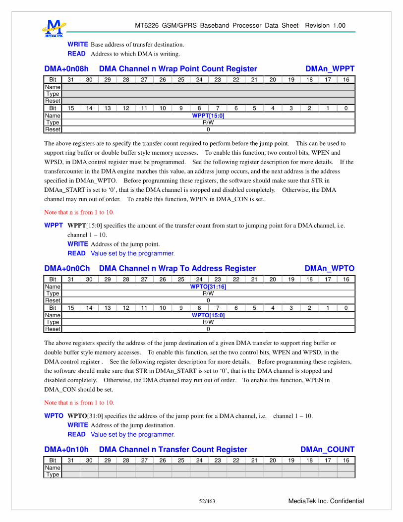
MT6226 GSM/GPRS Baseband Processor Data Sheet Revision 1.00
52/463 MediaTek Inc. Confidential
WRITE Base address of transfer destination. READ Address to which DMA is writing.
DMA+0n08h DMA Channel n Wrap Point Count Register DMAn_WPPT Bit 31 30 29 28 27 26 25 24 23 22 21 20 19 18 17 16
Name Type Reset
Bit 15 14 13 12 11 10 9 8 7 6 5 4 3 2 1 0 Name WPPT[15:0] Type R/W Reset 0
The above registers are to specify the transfer count required to perform before the jump point. This can be used to support ring buffer or double buffer style memory accesses. To enable this function, two control bits, WPEN and WPSD, in DMA control register must be programmed. See the following register description for more details. If the transfercounter in the DMA engine matches this value, an address jump occurs, and the next address is the address specified in DMAn_WPTO. Before programming these registers, the software should make sure that STR in DMAn_START is set to ‘0’, that is the DMA channel is stopped and disabled completely. Otherwise, the DMA channel may run out of order. To enable this function, WPEN in DMA_CON is set.
Note that n is from 1 to 10.
WPPT WPPT[15:0] specifies the amount of the transfer count from start to jumping point for a DMA channel, i.e. channel 1 – 10. WRITE Address of the jump point. READ Value set by the programmer.
DMA+0n0Ch DMA Channel n Wrap To Address Register DMAn_WPTO Bit 31 30 29 28 27 26 25 24 23 22 21 20 19 18 17 16
Name WPTO[31:16] Type R/W Reset 0
Bit 15 14 13 12 11 10 9 8 7 6 5 4 3 2 1 0 Name WPTO[15:0] Type R/W Reset 0
The above registers specify the address of the jump destination of a given DMA transfer to support ring buffer or double buffer style memory accesses. To enable this function, set the two control bits, WPEN and WPSD, in the DMA control register . See the following register description for more details. Before programming these registers, the software should make sure that STR in DMAn_START is set to ‘0’, that is the DMA channel is stopped and disabled completely. Otherwise, the DMA channel may run out of order. To enable this function, WPEN in DMA_CON should be set.
Note that n is from 1 to 10.
WPTO WPTO[31:0] specifies the address of the jump point for a DMA channel, i.e. channel 1 – 10. WRITE Address of the jump destination. READ Value set by the programmer.
DMA+0n10h DMA Channel n Transfer Count Register DMAn_COUNT Bit 31 30 29 28 27 26 25 24 23 22 21 20 19 18 17 16
Name Type

MT6226 GSM/GPRS Baseband Processor Data Sheet Revision 1.00
53/463 MediaTek Inc. Confidential
Reset Bit 15 14 13 12 11 10 9 8 7 6 5 4 3 2 1 0
Name LEN Type R/W Reset 0
This register specifies the amount of total transfer count that the DMA channel is required to perform. Upon completion, the DMA channel generates an interrupt request to the processor while ITEN in DMAn_CON is set as ‘1’. Note that the total size of data being transferred by a DMA channel is determined by LEN together with the SIZE in DMAn_CON, i.e. LEN x SIZE.
For virtual FIFO DMA, this register is used to configure the RX threshold and TX threshold. Interrupt is triggered while FIFO count >= RX threshold in RX path or FIFO count =< TX threshold in TX path. Note that ITEN bit in DMA_CON register shall be set, or no interrupt is issued.
Note that n is from 1 to 14.
LEN The amount of total transfer count
DMA+0n14h DMA Channel n Control Register DMAn_CON Bit 31 30 29 28 27 26 25 24 23 22 21 20 19 18 17 16
Name MAS DIR WPEN WPSD
Type R/W R/W R/W R/W Reset 0 0 0 0
Bit 15 14 13 12 11 10 9 8 7 6 5 4 3 2 1 0 Name ITEN BURST B2W DRQ DINC SINC SIZE Type R/W R/W R/W R/W R/W R/W R/W Reset 0 0 0 0 0 0 0
This register contains all the available control schemes for a DMA channel that is ready for software programmer to configure. Note that all these fields cannot be changed while DMA transfer is in progress or an unexpected situation may occur.
Note that n is from 1 to 14.
SIZE Data size within the confine of a bus cycle per transfer. These bits confines the data transfer size between source and destination to the specified value for individual
bus cycle. The size is in terms of byte and has maximum value of 4 bytes. It is mainly decided by the data width of a DMA master. 00 Byte transfer/1 byte 01 Half-word transfer/2 bytes 10 Word transfer/4 bytes 11 Reserved
SINC Incremental source address. Source addresses increase every transfer. If the setting of SIZE is Byte, Source addresses increase by 1 every single transfer. If Half-Word, increase by 2; and if Word, increase by 4. 0 Disable 1 Enable
DINC Incremental destination address. Destination addresses increase every transfer. If the setting of SIZE is Byte, Destination addresses increase by 1 every single transfer. If Half-Word, increase by 2; and Iif Word, increase by 4. 0 Disable 1 Enable
DREQ Throttle and handshake control for DMA transfer

MT6226 GSM/GPRS Baseband Processor Data Sheet Revision 1.00
54/463 MediaTek Inc. Confidential
0 No throttle control during DMA transfer or transfers occurred only between memories 1 Hardware handshake management
The DMA master is able to throttle down the transfer rate by way of request-grant handshake. B2W Word to Byte or Byte to Word transfer for the applications of transferring non-word-aligned-address data to
word-aligned-address data. Note that BURST is set to 4-beat burst while enabling this function, and the SIZE is set to Byte.
NO effect on channel 1 – 3 & 11 - 14. 0 Disable 1 Enable
BURST Transfer Type. Burst-type transfers have better bus efficiency. Mass data movement is recommended to use this kind of transfer. However, note that burst-type transfer does not stop until all of the beats in a burst are completed or transfer length is reached. FIFO threshold of peripherals must be configured carefully while being used to move data from/to the peripherals.
What transfer type can be used is restricted by the SIZE. If SIZE is 00b, i.e. byte transfer, all of the four transfer types can be used. If SIZE is 01b, i.e. half-word transfer, 16-beat incrementing burst cannot be used. If SIZE is 10b, i.e. byte transfer, only single and 4-beat incrementing burst can be used.
NO effect on channel 11 - 14. 000 Single 001 Reserved 010 4-beat incrementing burst 011 Reserved 100 8-beat incrementing burst 101 Reserved 110 16-beat incrementing burst 111 Reserved
ITEN DMA transfer completion interrupt enable. 0 Disable 1 Enable
WPSD The side using address-wrapping function. Only one side of a DMA channel can activate address-wrapping function at a time.
NO effect on channel 11 - 14. 0 Address-wrapping on source . 1 Address-wrapping on destination.
WPEN Address-wrapping for ring buffer. The next address of DMA jumps to WRAP TO address when the current address matches WRAP POINT count.
NO effect on channel 11 - 14. 0 Disable 1 Enable
DIR Directions of DMA transfer for half-size and Virtual FIFO DMA channels, i.e. channels 4~14. The direction is from the perspective of the DMA masters. WRITE means read from master and then write to the address specified in DMA_PGMADDR, and vice versa.
NO effect on channel 1 - 3. 0 Read 1 Write
MAS Master selection. Specifies which master occupies this DMA channel. Once assigned to certain master, the corresponding DREQ and DACK are connected. For half-size and Virtual FIFO DMA channels, i.e. channels 4 ~ 14, a predefined address is assigned as well.

MT6226 GSM/GPRS Baseband Processor Data Sheet Revision 1.00
55/463 MediaTek Inc. Confidential
00000 SIM 00001 MSDC 00010 IrDA TX 00011 IrDA RX 00100 USB1 Write 00101 USB1 Read 00110 USB2 Write 00111 USB2 Read 01000 UART1 TX 01001 UART1 RX 01010 UART2 TX 01011 UART2 RX 01100 UART3 TX 01101 UART3 RX 01110 DSP-DMA 01111 NFI TX 10000 NFI RX OTHERS Reserved
DMA+0n18h DMA Channel n Start Register DMAn_START Bit 31 30 29 28 27 26 25 24 23 22 21 20 19 18 17 16
Name Type Reset
Bit 15 14 13 12 11 10 9 8 7 6 5 4 3 2 1 0 Name STR Type R/W Reset 0
This register controls the activity of a DMA channel. Note that prior to setting STR to “1”, all the configurations should be done by giving proper value to the registers. Note also that once the STR is set to “1”, the hardware does not clear it automatically no matter if the DMA channel accomplishes the DMA transfer or not. In other works, the value of STR stays “1” regardless of the completion of DMA transfer. Therefore, the software program should be sure to clear STR to “0” before restarting another DMA transfer.
Note that n is from 1 to 14.
STR Start control for a DMA channel. 0 The DMA channel is stopped. 1 The DMA channel is started and running.
DMA+0n1Ch DMA Channel n Interrupt Status Register DMAn_INTSTA Bit 31 30 29 28 27 26 25 24 23 22 21 20 19 18 17 16
Name Type Reset
Bit 15 14 13 12 11 10 9 8 7 6 5 4 3 2 1 0 Name INT Type RO Reset 0
This register shows the interrupt status of a DMA channel. It has the same value as DMA_GLBSTA.
Note that n is from 1 to 14.

MT6226 GSM/GPRS Baseband Processor Data Sheet Revision 1.00
56/463 MediaTek Inc. Confidential
INT Interrupt Status for DMA Channel 0 No interrupt request is generated. 1 One interrupt request is pending and waiting for service.
DMA+0n20h DMA Channel n Interrupt Acknowledge Register DMAn_ACKINT Bit 31 30 29 28 27 26 25 24 23 22 21 20 19 18 17 16
Name Type Reset
Bit 15 14 13 12 11 10 9 8 7 6 5 4 3 2 1 0 Name ACK Type WO Reset 0
This register is used to acknowledge the current interrupt request associated with the completion event of a DMA channel by software program. Note that this is a write-only register, and any read to it returns a value of “0”.
Note that n is from 1 to 14.
ACK Interrupt acknowledge for the DMA channel 0 No effect 1 Interrupt request is acknowledged and should be relinquished.
DMA+0n24h DMA Channel n Remaining Length of Current Transfer
DMAn_RLCT
Bit 31 30 29 28 27 26 25 24 23 22 21 20 19 18 17 16 Name Type Reset
Bit 15 14 13 12 11 10 9 8 7 6 5 4 3 2 1 0 Name RLCT Type RO Reset 0
This register is to reflect the left amount of the transfer. Note that n is from 1 to 10.
DMA+0n28h DMA Bandwidth limiter Register DMAn_LIMITER Bit 31 30 29 28 27 26 25 24 23 22 21 20 19 18 17 16
Name Type Reset
Bit 15 14 13 12 11 10 9 8 7 6 5 4 3 2 1 0 Name LIMITER Type R/W Reset 0
This register is to suppress the Bus utilization of the DMA channel. The value is from 0 to 255. 0 means no limitation, and 255 means totally banned. The value between 0 and 255 means certain DMA can have permission to use AHB every (4 X n) AHB clock cycles. Note that it is not recommended to limit the Bus utilization of the DMA channels because this increases the latency of response to the masters, and the transfer rate decreases as well. Before using it, programmer must make sure that the bus masters have some protective mechanism to avoid entering the wrong states. Note that n is from 1 to 14.

MT6226 GSM/GPRS Baseband Processor Data Sheet Revision 1.00
57/463 MediaTek Inc. Confidential
LIMITER from 0 to 255. 0 means no limitation, 255 means totally banned, and others mean Bus access permission every (4 X n) AHB clock.
DMA+0n2Ch DMA Channel n Programmable Address Register DMAn_PGMAD
DR Bit 31 30 29 28 27 26 25 24 23 22 21 20 19 18 17 16
Name PGMADDR[31:16] Type R/W Reset 0
Bit 15 14 13 12 11 10 9 8 7 6 5 4 3 2 1 0 Name PGMADDR[15:0] Type R/W Reset 0
The above registers specify the address for a half-size DMA channel. This address represents a source address if DIR in DMA_CON is set to 0, and represents a destination address if DIR in DMA_CON is set to 1. Before being able to program these register, the software should make sure that STR in DMAn_START is set to ‘0’, that is the DMA channel is stopped and disabled completely. Otherwise, the DMA channel may run out of order.
Note that n is from 4 to 14.
PGMADDR PGMADDR[31:0] specifies the addresses for a half-size or a Virtual FIFO DMA channel, i.e. channel 4 – 14. WRITE Address of the jump destination. READ Current address of the transfer.
DMA+0n30h DMA Channel n Virtual FIFO Write Pointer Register DMAn_WRPTR Bit 31 30 29 28 27 26 25 24 23 22 21 20 19 18 17 16
Name WRPTR[31:16] Type RO Bit 15 14 13 12 11 10 9 8 7 6 5 4 3 2 1 0
Name WRPTR[15:0] Type RO
Note that n is from 11 to 14.
WRPTR Virtual FIFO Write Pointer.
DMA+0n34h DMA Channel n Virtual FIFO Read Pointer Register DMAn_RDPTR Bit 31 30 29 28 27 26 25 24 23 22 21 20 19 18 17 16
Name RDPTR[31:16] Type RO Bit 15 14 13 12 11 10 9 8 7 6 5 4 3 2 1 0
Name RDPTR[15:0] Type RO
Note that n is from 11 to 14.
RDPTR Virtual FIFO Read Pointer.
DMA+0n38h DMA Channel n Virtual FIFO Data Count Register DMAn_FFCNT Bit 31 30 29 28 27 26 25 24 23 22 21 20 19 18 17 16
Name Type Bit 15 14 13 12 11 10 9 8 7 6 5 4 3 2 1 0
Name FFCNT Type RO

MT6226 GSM/GPRS Baseband Processor Data Sheet Revision 1.00
58/463 MediaTek Inc. Confidential
Note that n is from 11 to 14.
FFCNT To display the number of data stored in FIFO. 0 means FIFO empty, and FIFO is full if FFCNT is equal to FFSIZE.
DMA+0n3Ch DMA Channel n Virtual FIFO Status Register DMAn_FFSTA Bit 31 30 29 28 27 26 25 24 23 22 21 20 19 18 17 16
Name Type Reset
Bit 15 14 13 12 11 10 9 8 7 6 5 4 3 2 1 0
Name ALT EMPTY FULL
Type RO RO RO Reset 0 1 0
Note that n is from 11 to 14.
FULL To indicate FIFO is full. 0 Not Full 1 Full
EMPTY To indicate FIFO is empty. 0 Not Empty 1 Empty
ALT To indicate FIFO Count is larger than ALTLEN. DMA issues an alert signal to UART to enable UART flow control. 0 Not reach alert region. 1 Reach alert region.
DMA+0n40h DMA Channel n Virtual FIFO Alert Length Register DMAn_ALTLEN Bit 31 30 29 28 27 26 25 24 23 22 21 20 19 18 17 16
Name Type Reset
Bit 15 14 13 12 11 10 9 8 7 6 5 4 3 2 1 0 Name ALTLEN Type R/W Reset 0
Note that n is from 11 to 14.
ALTLEN Specifies the Alert Length of Virtual FIFO DMA. Once the remaining FIFO space is less than ALTLEN, an alert signal is issued to UART to enable flow control. Normally, ALTLEN shall be larger than 16 for UART application.
DMA+0n44h DMA Channel n Virtual FIFO Size Register DMAn_FFSIZE Bit 31 30 29 28 27 26 25 24 23 22 21 20 19 18 17 16
Name Type Reset
Bit 15 14 13 12 11 10 9 8 7 6 5 4 3 2 1 0 Name FFSIZE Type R/W Reset 0
Note that n is from 11 to 14.

MT6226 GSM/GPRS Baseband Processor Data Sheet Revision 1.00
59/463 MediaTek Inc. Confidential
FFSIZE Specifies the FIFO Size of Virtual FIFO DMA.
3.5 Interrupt Controller
3.5.1 General Description Figure 35 outlines the major functionality of the MCU Interrupt Controller. The interrupt controller processes all interrupt sources coming from external lines and internal MCU peripherals. Since ARM7EJ-S core supports two levels of interrupt latency, this controller generates two request signals: FIQ for fast, low latency interrupt request and IRQ for more general interrupts with lower priority.
InterruptInput
MultiplexIRQ
ControllerIRQn
IRQ0
IRQ1
IRQ2
IRQ31
KP
TDMA
GPT
SIM
UART1
DSP2MCU
RTC
UART2
EINT FIQ
IRQ
FIQController
Registers
SoftIRQ
APB Bus
Figure 35 Block Diagram of the Interrupt Controller
One and only one of the interrupt sources can be assigned to FIQ Controller and have the highest priority in requesting timing critical service. All the others share the same IRQ signal by connecting them to IRQ Controller. The IRQ Controller manages up 32 interrupt lines of IRQ0 to IRQ31 with fixed priority in descending order.
The Interrupt Controller provides a simple software interface by mean of registers to manipulate the interrupt request shared system. IRQ Selection Registers and FIQ Selection Register determine the source priority and connecting relation among sources and interrupt lines. IRQ Source Status Register allows software program to identify the source of interrupt that generates the interrupt request. IRQ Mask Register provides software to mask out undesired sources some time. End of Interrupt Register permits software program to indicate to the controller that a certain interrupt service routine has been finished.
Binary coded version of IRQ Source Status Register is also made available for software program to helpfully identify the interrupt source. Note that while taking advantage of this, it should also take the binary coded version of End of Interrupt Register coincidently.
The essential Interrupt Table of ARM7EJ-S core is shown as Table 15.

MT6226 GSM/GPRS Baseband Processor Data Sheet Revision 1.00
60/463 MediaTek Inc. Confidential
Address Description
00000000h System Reset
00000018h IRQ
0000001Ch FIQ
Table 15 Interrupt Table of ARM7EJ-S
3.5.1.1 Interrupt Source Masking
Interrupt controller provides the function of Interrupt Source Masking by the way of programming MASK register. Any of them can be masked individually.
However, because of the bus latency, the masking takes effect no earlier than 3 clock cycles later. In this time, the to-be-masked interrupts could come in and generate an IRQ pulse to MCU, and then disappear immediately. This IRQ forces MCU going to Interrupt Service Routine and polling Status Register (IRQ_STA or IRQ_STA2), but the register shows there is no interrupt. This might cause MCU malfunction.
There are two ways for programmer to protect their software.
1. Return from ISR (Interrupt Service Routine) immediately while the Status register shows no interrupt.
2. Set I bit of MCU before doing Interrupt Masking, and then clear it after Interrupt Masking done.
Both avoid the problem, but the first item recommended to have in the ISR.
3.5.1.2 External Interrupt
This interrupt controller also integrates an External Interrupt Controller that can support up to 4 interrupt requests coming from external sources, the EINT0~3, and 4 WakeUp interrupt requests, i.e. EINT4~7, coming from peripherals used to inform system to resume the system clock.
The four external interrupts can be used for different kind of applications, mainly for event detections: detection of hand free connection, detection of hood opening, detection of battery charger connection.
Since the external event may be unstable in a certain period, a de-bounce mechanism is introduced to ensure the functionality. The circuitry is mainly used to verify that the input signal remains stable for a programmable number of periods of the clock. When this condition is satisfied, for the appearance or the disappearance of the input, the output of the de-bounce logic changes to the desired state. Note that, because it uses the 32 KHz slow clock for performing the de-bounce process, the parameter of de-bounce period and de-bounce enable takes effect no sooner than one 32 KHz clock cycle (~31.25us) after the software program sets them. However, the polarities of EINTs are clocked with the system clock. Any changes to them take effect immediately. Note also that this External Interrupt Controller handles only level sensitive type of interrupt sources.

MT6226 GSM/GPRS Baseband Processor Data Sheet Revision 1.00
61/463 MediaTek Inc. Confidential
Debounce Logic
Debounce Logic
Debounce Logic
Registers
InterruptControlLogic
EINT_IRQ
EINT3
EINT1
EINT2
APB Bus
MT6227
Debounce LogicEINT0
Debounce Logic
Debounce Logic
Debounce Logic
EINT7
EINT5
EINT6
Debounce LogicEINT4
Figure 36 Block of External Interrupt Controller
REGISTER ADDRESS REGISTER NAME SYNONYM
CIRQ + 0000h IRQ Selection 0 Register IRQ_SEL0
CIRQ + 0004h IRQ Selection 1 Register IRQ_SEL1
CIRQ + 0008h IRQ Selection 2 Register IRQ_SEL2
CIRQ + 000Ch IRQ Selection 3 Register IRQ_SEL3
CIRQ + 0010h IRQ Selection 4 Register IRQ_SEL4
CIRQ + 0014h IRQ Selection 5 Register IRQ_SEL5
CIRQ + 0018h FIQ Selection Register FIQ_SEL
CIRQ + 001Ch IRQ Mask Register IRQ_MASK
CIRQ + 0020h IRQ Mask Disable Register IRQ_MASK_DIS
CIRQ + 0024h IRQ Mask Enable Register IRQ_MASK_EN
CIRQ + 0028h IRQ Status Register IRQ_STA
CIRQ + 002Ch IRQ End of Interrupt Register IRQ_EOI
CIRQ + 0030h IRQ Sensitive Register IRQ_SENS
CIRQ + 0034h IRQ Software Interrupt Register IRQ_SOFT
CIRQ + 0038h FIQ Control Register FIQ_CON
CIRQ + 003Ch FIQ End of Interrupt Register FIQ_EOI
CIRQ + 0040h Binary Coded Value of IRQ_STATUS IRQ_STA2
CIRQ + 0044h Binary Coded Value of IRQ_EOI IRQ_EOI2
CIRQ + 0100h EINT Status Register EINT_STA
CIRQ + 0104h EINT Mask Register EINT_MASK
CIRQ + 0108h EINT Mask Disable Register EINT_MASK_DIS
CIRQ + 010Ch EINT Mask Enable Register EINT_MASK_EN
CIRQ + 0110h EINT Interrupt Acknowledge Register EINT_INTACK
CIRQ + 0114h EINT Sensitive Register EINT_SENS
CIRQ + 0120h EINT0 De-bounce Control Register EINT0_CON
CIRQ + 0130h EINT1 De-bounce Control Register EINT1_CON

MT6226 GSM/GPRS Baseband Processor Data Sheet Revision 1.00
62/463 MediaTek Inc. Confidential
CIRQ + 0140h EINT2 De-bounce Control Register EINT2_CON
CIRQ + 0150h EINT3 De-bounce Control Register EINT3_CON
CIRQ + 0160h EINT4 De-bounce Control Register EINT4_CON
CIRQ + 0170h EINT5 De-bounce Control Register EINT5_CON
CIRQ + 0180h EINT6 De-bounce Control Register EINT6_CON
CIRQ + 0190h EINT7 De-bounce Control Register EINT7_CON
Table 16 Interrupt Controller Register Map
3.5.2 Register Definitions
CIRQ+0000h IRQ Selection 0 Register IRQ_SEL0 Bit 31 30 29 28 27 26 25 24 23 22 21 20 19 18 17 16
Name IRQ5 IRQ4 IRQ3 Type R/W R/W R/W Reset 5 4 3
Bit 15 14 13 12 11 10 9 8 7 6 5 4 3 2 1 0 Name IRQ2 IRQ1 IRQ0 Type R/W R/W R/W Reset 2 1 0
CIRQ+0004h IRQ Selection 1 Register IRQ_SEL1 Bit 31 30 29 28 27 26 25 24 23 22 21 20 19 18 17 16
Name IRQB IRQA IRQ9 Type R/W R/W R/W Reset B A 9
Bit 15 14 13 12 11 10 9 8 7 6 5 4 3 2 1 0 Name IRQ8 IRQ7 IRQ6 Type R/W R/W R/W Reset 8 7 6
CIRQ+0008h IRQ Selection 2 Register IRQ_SEL2 Bit 31 30 29 28 27 26 25 24 23 22 21 20 19 18 17 16
Name IRQ11 IRQ10 IRQF Type R/W R/W R/W Reset 11 10 F
Bit 15 14 13 12 11 10 9 8 7 6 5 4 3 2 1 0 Name IRQE IRQD IRQC Type R/W R/W R/W Reset E D C
CIRQ+000Ch IRQ Selection 3 Register IRQ_SEL3 Bit 31 30 29 28 27 26 25 24 23 22 21 20 19 18 17 16
Name IRQ17 IRQ16 IRQ15 Type R/W R/W R/W Reset 17 16 15
Bit 15 14 13 12 11 10 9 8 7 6 5 4 3 2 1 0 Name IRQ14 IRQ13 IRQ12 Type R/W R/W R/W Reset 14 13 12

MT6226 GSM/GPRS Baseband Processor Data Sheet Revision 1.00
63/463 MediaTek Inc. Confidential
CIRQ+0010h IRQ Selection 4 Register IRQ_SEL4 Bit 31 30 29 28 27 26 25 24 23 22 21 20 19 18 17 16
Name IRQ1D IRQ1C IRQ1B Type R/W R/W R/W Reset 1D 1C 1B
Bit 15 14 13 12 11 10 9 8 7 6 5 4 3 2 1 0 Name IRQ1A IRQ19 IRQ18 Type R/W R/W R/W Reset 1A 19 18
CIRQ+0014h IRQ Selection 5 Register IRQ_SEL5 Bit 31 30 29 28 27 26 25 24 23 22 21 20 19 18 17 16
Name Type Reset
Bit 15 14 13 12 11 10 9 8 7 6 5 4 3 2 1 0 Name IRQ1F IRQ1E Type R/W R/W Reset 1F 1E
CIRQ+0018h FIQ Selection Register FIQ_SEL Bit 31 30 29 28 27 26 25 24 23 22 21 20 19 18 17 16
Name Type Reset
Bit 15 14 13 12 11 10 9 8 7 6 5 4 3 2 1 0 Name FIQ Type R/W Reset 0
The IRQ/FIQ Selection Registers provide system designers with a flexible routing scheme to make various mappings of priority among interrupt sources possible. The registers allow the interrupt sources to be mapped onto interrupt requests of either FIQ or IRQ. While only one interrupt source can be assigned to FIQ, the other ones share IRQs by mapping them onto IRQ0 to IRQ1F connected to IRQ controller. The priority sequence of IRQ0~IRQ1F is fixed, i.e. IRQ0 > IRQ1 > IRQ2 > … > IRQ1E > IRQ1F. During the software configuration process, the Interrupt Source Code of desired interrupt source should be written into source field of the corresponding IRQ_SEL0-IRQ_SEL4/FIQ_SEL. Five-bit Interrupt Source Codes for all interrupt sources are fixed and defined.
Interrupt Source STA2 (Hex) STA
MFIQ 0 00000001
TDMA_CTIRQ1 1 00000002
TDMA_CTIRQ2 2 00000004
DSP2CPU 3 00000008
SIM 4 00000010
DMA 5 00000020
TDMA 6 00000040
UART1 7 00000080
KeyPad 8 00000100
UART2 9 00000200
GPTimer A 00000400

MT6226 GSM/GPRS Baseband Processor Data Sheet Revision 1.00
64/463 MediaTek Inc. Confidential
EINT B 00000800
USB C 00001000
MSDC D 00002000
RTC E 00004000
IrDA F 00008000
LCD 10 00010000
UART3 11 00020000
MIRQ 12 00040000
WDT 13 00080000
JPEG 14 00100000
Resizer 15 00200000
NFI 16 00400000
B2PSI 17 00800000
Image DMA 18 01000000
MSDC_CD_IRQ 1a 04000000
SCCB 1b 08000000
G2D 1c 10000000
Image Engine 1d 20000000
CAM 1e 40000000
MPEG4 1f 80000000
Table 17 Interrupt Source Code for Interrupt Sources
FIQ, IRQ0-1F The 5-bit content of this field corresponds to an Interrupt Source Code shown above.
CIRQ+001Ch IRQ Mask Register IRQ_MASK Bit 31 30 29 28 27 26 25 24 23 22 21 20 19 18 17 16
Name IRQ1F IRQ1E IRQ1D
IRQ1C
IRQ1B
IRQ1A IRQ19 IRQ18 IRQ17 IRQ16 IRQ15 IRQ14 IRQ13 IRQ12 IRQ11 IRQ10
Type R/W R/W R/W R/W R/W R/W R/W R/W R/W R/W R/W R/W R/W R/W R/W R/W Reset 1 1 1 1 1 1 1 1 1 1 1 1 1 1 1 1
Bit 15 14 13 12 11 10 9 8 7 6 5 4 3 2 1 0 Name IRQF IRQE IRQD IRQC IRQB IRQA IRQ9 IRQ8 IRQ7 IRQ6 IRQ5 IRQ4 IRQ3 IRQ2 IRQ1 IRQ0 Type R/W R/W R/W R/W R/W R/W R/W R/W R/W R/W R/W R/W R/W R/W R/W R/W Reset 1 1 1 1 1 1 1 1 1 1 1 1 1 1 1 1
This register contains a mask bit for each interrupt line in IRQ Controller. The register allows each interrupt source IRQ0 to IRQ1F to be disabled or masked separately under software control. After a system reset, all bit values are set to 1 to indicate that interrupt requests are prohibited.
IRQ0-1F Mask control for the associated interrupt source in the IRQ controller 0 Interrupt is enabled 1 Interrupt is disabled
CIRQ+0020h IRQ Mask Clear Register IRQ_MASK_CL
R Bit 31 30 29 28 27 26 25 24 23 22 21 20 19 18 17 16
Name IRQ1F IRQ1E IRQ1D
IRQ1C
IRQ1B
IRQ1A IRQ19 IRQ18 IRQ17 IRQ16 IRQ15 IRQ14 IRQ13 IRQ12 IRQ11 IRQ10
Type W1C W1C W1C W1C W1C W1C W1C W1C W1C W1C W1C W1C W1C W1C W1C W1C

MT6226 GSM/GPRS Baseband Processor Data Sheet Revision 1.00
65/463 MediaTek Inc. Confidential
Bit 15 14 13 12 11 10 9 8 7 6 5 4 3 2 1 0 Name IRQF IRQE IRQD IRQC IRQB IRQA IRQ9 IRQ8 IRQ7 IRQ6 IRQ5 IRQ4 IRQ3 IRQ2 IRQ1 IRQ0 Type W1C W1C W1C W1C W1C W1C W1C W1C W1C W1C W1C W1C W1C W1C W1C W1C
This register is used to clear bits in IRQ Mask Register. When writing to this register, the data bits that are HIGH cause the corresponding bits in IRQ Mask Register to be cleared. Data bits that are LOW have no effect on the corresponding bits in IRQ Mask Register.
IRQ0-1F Clear corresponding bits in IRQ Mask Register. 0 No effect 1 Disable the corresponding MASK bit
CIRQ+0024h IRQ Mask SET Register IRQ_MASK_SE
T Bit 31 30 29 28 27 26 25 24 23 22 21 20 19 18 17 16
Name IRQ1F IRQ1E IRQ1D
IRQ1C
IRQ1B
IRQ1A IRQ19 IRQ18 IRQ17 IRQ16 IRQ15 IRQ14 IRQ13 IRQ12 IRQ11 IRQ10
Type W1S W1S W1S W1S W1S W1S W1S W1S W1S W1S W1S W1S W1S W1S W1S W1S Bit 15 14 13 12 11 10 9 8 7 6 5 4 3 2 1 0
Name IRQF IRQE IRQD IRQC IRQB IRQA IRQ9 IRQ8 IRQ7 IRQ6 IRQ5 IRQ4 IRQ3 IRQ2 IRQ1 IRQ0 Type W1S W1S W1S W1S W1S W1S W1S W1S W1S W1S W1S W1S W1S W1S W1S W1S
This register is used to set bits in the IRQ Mask Register. When writing to this register, the data bits that are HIGH cause the corresponding bits in IRQ Mask Register to be set. Data bits that are LOW have no effect on the corresponding bits in IRQ Mask Register.
IRQ0-1F Set corresponding bits in IRQ Mask Register. 0 No effect 1 Enable corresponding MASK bit
CIRQ+0028h IRQ Source Status Register IRQ_STA Bit 31 30 29 28 27 26 25 24 23 22 21 20 19 18 17 16
Name IRQ1F IRQ1E IRQ1D
IRQ1C
IRQ1B
IRQ1A IRQ19 IRQ18 IRQ17 IRQ16 IRQ15 IRQ14 IRQ13 IRQ12 IRQ11 IRQ10
Type RO RO RO RO RO RO RO RO RO RO RO RO RO RO RO RO Reset 0 0 0 0 0 0 0 0 0 0 0 0 0 0 0 0
Bit 15 14 13 12 11 10 9 8 7 6 5 4 3 2 1 0 Name IRQF IRQE IRQD IRQC IRQB IRQA IRQ9 IRQ8 IRQ7 IRQ6 IRQ5 IRQ4 IRQ3 IRQ2 IRQ1 IRQ0 Type RO RO RO RO RO RO RO RO RO RO RO RO RO RO RO RO Reset 0 0 0 0 0 0 0 0 0 0 0 0 0 0 0 0
This Register allows software to poll which interrupt line has generated an IRQ interrupt request. A bit set to 1 indicates a corresponding active interrupt line. Only one flag is active at a time. The IRQ_STA is type of read-clear; write access has no effect on the content.
IRQ0-1F Interrupt indicator for the associated interrupt source. 0 The associated interrupt source is non-active. 1 The associated interrupt source is asserted.
CIRQ+002Ch IRQ End of Interrupt Register IRQ_EOI Bit 31 30 29 28 27 26 25 24 23 22 21 20 19 18 17 16
Name IRQ1F IRQ1E IRQ1D
IRQ1C
IRQ1B
IRQ1A IRQ19 IRQ18 IRQ17 IRQ16 IRQ15 IRQ14 IRQ13 IRQ12 IRQ11 IRQ10
Type WO WO WO WO WO WO WO WO WO WO WO WO WO WO WO WO Reset 0 0 0 0 0 0 0 0 0 0 0 0 0 0 0 0
Bit 15 14 13 12 11 10 9 8 7 6 5 4 3 2 1 0

MT6226 GSM/GPRS Baseband Processor Data Sheet Revision 1.00
66/463 MediaTek Inc. Confidential
Name IRQF IRQE IRQD IRQC IRQB IRQA IRQ9 IRQ8 IRQ7 IRQ6 IRQ5 IRQ4 IRQ3 IRQ2 IRQ1 IRQ0 Type WO WO WO WO WO WO WO WO WO WO WO WO WO WO WO WO Reset 0 0 0 0 0 0 0 0 0 0 0 0 0 0 0 0
This register provides a mean for software to relinquish and to refresh the interrupt controller. Writing a 1 to a specific bit position results in an End of Interrupt command issued internally to the corresponding interrupt line.
IRQ0-1F End of Interrupt command for the associated interrupt line. 0 No service is currently in progress or pending 1 Interrupt request is in-service
CIRQ+0030h IRQ Sensitive Register IRQ_SENS Bit 31 30 29 28 27 26 25 24 23 22 21 20 19 18 17 16
Name IRQ1F IRQ1E IRQ1D
IRQ1C
IRQ1B
IRQ1A IRQ19 IRQ18 IRQ17 IRQ16 IRQ15 IRQ14 IRQ13 IRQ12 IRQ11 IRQ10
Type R/W R/W R/W R/W R/W R/W R/W R/W R/W R/W R/W R/W R/W R/W R/W R/W Reset 0 0 0 0 0 0 0 0 0 0 0 0 0 0 0 0
Bit 15 14 13 12 11 10 9 8 7 6 5 4 3 2 1 0 Name IRQF IRQE IRQD IRQC IRQB IRQA IRQ9 IRQ8 IRQ7 IRQ6 IRQ5 IRQ4 IRQ3 IRQ2 IRQ1 IRQ0 Type R/W R/W R/W R/W R/W R/W R/W R/W R/W R/W R/W R/W R/W R/W R/W R/W Reset 0 0 0 0 0 0 0 0 0 0 0 0 0 0 0 0
All interrupt lines of IRQ Controller, IRQ0~IRQ1F can be programmed as either edge or level sensitive. By default, all the interrupt lines are edge sensitive and should be active LOW. Once a interrupt line is programmed as edge sensitive, an interrupt request is triggered only at the falling edge of interrupt line, and the next interrupt is not accepted until the EOI command is given. However, level sensitive interrupts trigger is according to the signal level of the interrupt line. Once the interrupt line become from HIGH to LOW, an interrupt request is triggered, and another interrupt request is triggered if the signal level remain LOW after an EOI command. Note that in edge sensitive mode, even if the signal level remains LOW after EOI command, another interrupt request is not triggered. That is because edge sensitive interrupt is only triggered at the falling edge.
IRQ0-1F Sensitivity type of the associated Interrupt Source 0 Edge sensitivity with active LOW 1 Level sensitivity with active LOW
CIRQ+0034h IRQ Software Interrupt Register IRQ_SOFT Bit 31 30 29 28 27 26 25 24 23 22 21 20 19 18 17 16
Name IRQ1F IRQ1E IRQ1D
IRQ1C
IRQ1B
IRQ1A IRQ19 IRQ18 IRQ17 IRQ16 IRQ15 IRQ14 IRQ13 IRQ12 IRQ11 IRQ10
Type R/W R/W R/W R/W R/W R/W R/W R/W R/W R/W R/W R/W R/W R/W R/W R/W Reset 0 0 0 0 0 0 0 0 0 0 0 0 0 0 0 0
Bit 15 14 13 12 11 10 9 8 7 6 5 4 3 2 1 0 Name IRQF IRQE IRQD IRQC IRQB IRQA IRQ9 IRQ8 IRQ7 IRQ6 IRQ5 IRQ4 IRQ3 IRQ2 IRQ1 IRQ0 Type R/W R/W R/W R/W R/W R/W R/W R/W R/W R/W R/W R/W R/W R/W R/W R/W Reset 0 0 0 0 0 0 0 0 0 0 0 0 0 0 0 0
Setting “1” to the specific bit position generates a software interrupt for corresponding interrupt line before mask. This register is used for debug purpose.
IRQ0-IRQ1F Software Interrupt
CIRQ+0038h FIQ Control Register FIQ_CON Bit 31 30 29 28 27 26 25 24 23 22 21 20 19 18 17 16
Name Type Reset
Bit 15 14 13 12 11 10 9 8 7 6 5 4 3 2 1 0

MT6226 GSM/GPRS Baseband Processor Data Sheet Revision 1.00
67/463 MediaTek Inc. Confidential
Name SENS MASK
Type R/W R/W Reset 0 1
This register provides a means for software program to control the FIQ controller.
MASK Mask control for the FIQ Interrupt Source 0 Interrupt is enabled 1 Interrupt is disabled
SENS Sensitivity type of the FIQ Interrupt Source 0 Edge sensitivity with active LOW 1 Level sensitivity with active LOW
CIRQ+003Ch FIQ End of Interrupt Register FIQ_EOI Bit 31 30 29 28 27 26 25 24 23 22 21 20 19 18 17 16
Name Type Reset
Bit 15 14 13 12 11 10 9 8 7 6 5 4 3 2 1 0 Name EOI Type WO Reset 0
This register provides a means for software to relinquish and to refresh the FIQ controller. Writing a ‘1’ to the specific bit position results in an End of Interrupt command issued internally to the corresponding interrupt line.
EOI End of Interrupt command
CIRQ+0040h Binary Coded Value of IRQ_STATUS IRQ_STA2 Bit 31 30 29 28 27 26 25 24 23 22 21 20 19 18 17 16
Name Type Reset
Bit 15 14 13 12 11 10 9 8 7 6 5 4 3 2 1 0
Name NOIRQ STA
Type RO RO Reset 0 0
This Register is a binary coded version of IRQ_STA. It is used by the software program to poll which interrupt line has generated the IRQ interrupt request in a much easier way. Any read to it has the same result as reading IRQ_STA. The IRQ_STA2 is also read-only; write access has no effect on the content. Note that IRQ_STA2 should be coupled with IRQ_EOI2 while using it.
STA Binary coded value of IRQ_STA NOIRQ Indicating if there is an IRQ or not. If there is no IRQ, this bit is HIGH, and the value of STA is 0_0000b.
CIRQ+0044h Binary Coded Value of IRQ_EOI IRQ_EOI2 Bit 31 30 29 28 27 26 25 24 23 22 21 20 19 18 17 16
Name Type Reset
Bit 15 14 13 12 11 10 9 8 7 6 5 4 3 2 1 0 Name EOI Type WO Reset 0

MT6226 GSM/GPRS Baseband Processor Data Sheet Revision 1.00
68/463 MediaTek Inc. Confidential
This register is a binary coded version of IRQ_EOI. It provides an easier way for software program to relinquish and to refresh the interrupt controller. Writing a specific code results in an End of Interrupt command issued internally to the corresponding interrupt line. Note that IRQ_EOI2 should be coupled with IRQ_STA2 while using it.
EOI Binary coded value of IRQ_EOI
CIRQ+0100h EINT Interrupt Status Register EINT_STA Bit 31 30 29 28 27 26 25 24 23 22 21 20 19 18 17 16
Name Type Reset
Bit 15 14 13 12 11 10 9 8 7 6 5 4 3 2 1 0 Name EINT7 EINT6 EINT5 EINT4 EINT3 EINT2 EINT1 EINT0 Type RO RO RO RO RO RO RO RO Reset 0 0 0 0 0 0 0 0
This register keeps up with current status of which EINT Source generated the interrupt request. If EINT sources are set to edge sensitive, EINT_IRQ is de-asserted while this register is read.
EINT0-EINT7 Interrupt Status 0 No interrupt request is generated 1 Interrupt request is pending
CIRQ+0104h EINT Interrupt Mask Register EINT_MASK Bit 31 30 29 28 27 26 25 24 23 22 21 20 19 18 17 16
Name Type Reset
Bit 15 14 13 12 11 10 9 8 7 6 5 4 3 2 1 0 Name EINT7 EINT6 EINT5 EINT4 EINT3 EINT2 EINT1 EINT0 Type R/W R/W R/W R/W R/W R/W R/W R/W Reset 1 1 1 1 1 1 1 1
This register controls whether or not EINT Source is allowed to generate an interrupt request. Setting a “1” to the specific bit position prohibits the external interrupt line from becoming active.
EINT0-EINT7 Interrupt Mask 0 Interrupt request is enabled. 1 Interrupt request is disabled.
CIRQ+0108h EINT Interrupt Mask Clear Register EINT_MASK_C
LR Bit 31 30 29 28 27 26 25 24 23 22 21 20 19 18 17 16
Name Type Bit 15 14 13 12 11 10 9 8 7 6 5 4 3 2 1 0
Name EINT7 EINT6 EINT5 EINT4 EINT3 EINT2 EINT1 EINT0 Type W1C W1C W1C W1C W1C W1C W1C W1C
This register is used to clear individual mask bits. Only the bits set to 1 are in effect, and interrupt masks for which the mask bit is set are cleared (set to 0). Otherwise the interrupt mask bit retains its original value.
EINT0-EINT7 Disable mask for the associated external interrupt source 0 No effect. 1 Disable the corresponding MASK bit.

MT6226 GSM/GPRS Baseband Processor Data Sheet Revision 1.00
69/463 MediaTek Inc. Confidential
CIRQ+010Ch EINT Interrupt Mask Set Register EINT_MASK_S
ET Bit 31 30 29 28 27 26 25 24 23 22 21 20 19 18 17 16
Name Type Bit 15 14 13 12 11 10 9 8 7 6 5 4 3 2 1 0
Name EINT7 EINT6 EINT5 EINT4 EINT3 EINT2 EINT1 EINT0 Type W1S W1S W1S W1S W1S W1S W1S W1S
This register is used to set individual mask bits. Only the bits set to 1 are in effect, and interrupt masks for which the mask bit is set are set to 1. Otherwise the interrupt mask bit retains its original value.
EINT0-EINT7 Disable mask for the associated external interrupt source. 0 No effect. 1 Enable corresponding MASK bit.
CIRQ+0110h EINT Interrupt Acknowledge Register EINT_INTACK Bit 31 30 29 28 27 26 25 24 23 22 21 20 19 18 17 16
Name Type Reset
Bit 15 14 13 12 11 10 9 8 7 6 5 4 3 2 1 0 Name EINT7 EINT6 EINT5 EINT4 EINT3 EINT2 EINT1 EINT0 Type WO WO WO WO WO WO WO WO Reset 0 0 0 0 0 0 0 0
Writing “1” to the specific bit position acknowledge the interrupt request correspondingly to the external interrupt line source.
EINT0-EINT7 Interrupt acknowledgement 0 No effect. 1 Interrupt Request is acknowledged.
CIRQ+0114h EINT Sensitive Register EINT_SENS Bit 31 30 29 28 27 26 25 24 23 22 21 20 19 18 17 16
Name Type Reset
Bit 15 14 13 12 11 10 9 8 7 6 5 4 3 2 1 0 Name EINT7 EINT6 EINT5 EINT4 EINT3 EINT2 EINT1 EINT0 Type R/W R/W R/W R/W R/W R/W R/W R/W Reset 1 1 1 1 1 1 1 1
Sensitivity type of external interrupt source.
EINT0-7 Sensitive type of the associated external interrupt source 0 Edge sensitivity. 1 Level sensitivity.
CIRQ+01m0h EINTn De-bounce Control Register EINTn_CON Bit 31 30 29 28 27 26 25 24 23 22 21 20 19 18 17 16
Name Type Reset
Bit 15 14 13 12 11 10 9 8 7 6 5 4 3 2 1 0 Name EN POL CNT

MT6226 GSM/GPRS Baseband Processor Data Sheet Revision 1.00
70/463 MediaTek Inc. Confidential
Type R/W R/W R/W Reset 0 0 0
These registers control the de-bounce logic for external interrupt sources in order to minimize the possibility of false activations.
Note that n is from 0 to 7, and m is n + 2.
CNT De-bounce duration in terms of numbers of 32KHz clock cycles POL Activation type of the EINT source
0 Negative polarity 1 Positive polarity
EN De-bounce control circuit 0 Disable 1 Enable
3.6 Internal Memory Interface
3.6.1 System RAM MT6227 provides one 284 KByte size of on-chip memory modules acting as System RAM for data access with low latency. Such a module is composed of three high speed synchronous SRAMs with AHB Slave Interface connected to the system backbone AHB Bus, as shown in Figure 46. Bank0 and Bank1 SRAMs are 128Kbyte, and Bank2 SRAM is 28Kbyte. The synchronous SRAM operates on the same clock as the AHB Bus and is organized as 32 bits wide with 4 byte-write signals capable for byte operations. Bank0 and Bank1 SRAM macros have limited repair capability. The yield of SRAM is improved if the defects inside it can be repaired during testing.
3.6.2 System ROM The 27KByte System ROM is primarily used to store software program for Factory Programming. However, due to its advantageous low latency performance, some of the timing critical codes are also placed in System ROM. This module is composed of high-speed VIA ROM with an AHB Slave Interface connected to a system backbone AHB, shown in Figure 46. The module operates on the same clock as the AHB and has a 32-bit wide organization.

MT6226 GSM/GPRS Baseband Processor Data Sheet Revision 1.00
71/463 MediaTek Inc. Confidential
Figure 46: Block Diagram of the Internal Memory Controller
3.7 External Memory Interface
3.7.1 General Description MT6226 incorporates a powerful and flexible memory controller, External Memory Interface, to connect with a variety of memory components. This controller provides one generic access scheme for FLASH Memory, SRAM and PSRAM. Up to 8 memory banks can be supported simultaneously, BANK0-BANK7, with a maximum size of 64MB each
Since most of the FLASH Memory, SRAM and PSRAM have similar AC requirements, a generic configuration scheme to interface them is desired. This way, the software program can treat different components by simply specifying certain predefined parameters. All these parameters are based on cycle time of system clock.
The interface definition based on such scheme is listed in Table 18. Note that, this interface always operates data in Little Endian format for all types of accesses.
Signal Name Type Description
EA[25:0] O Address Bus
ED[15:0] I/O Data Bus
EWR# O Write Enable Strobe
ERD# O Read Enable Strobe
ELB# O Lower Byte Strobe
EUB# O Upper Byte Strobe
ECS# [7:0] O BANK0~BANK7 Selection Signal
EPDN O PSRAM Power Down Control Signal
ECLK O Burst Mode FLASH Memory Clock Signal
EADV# O Burst Mode FLASH Memory Address Latch Signal
Bank1 SRAM
Bank2 SRAM
DMA AHB BusLCD AHB Bus

MT6226 GSM/GPRS Baseband Processor Data Sheet Revision 1.00
72/463 MediaTek Inc. Confidential
EWAIT I Wait Signal Input
Table 18 External Memory Interface of MT6226 for Asynchronous/Synchronous Type Components
This controller can also handle parallel type of LCD. By connecting with them, 8080 type of control method is supported. The interface definition is detailed in Table 19.
Bus Type ECS7# EA25 ERD# EWR# ED[15:0]
8080 series CS# A0 RD# WR# D[15:0]
Table 19 Configuration for LCD Parallel Interface
REGISTER ADDRESS REGISTER NAME SYNONYM
EMI + 0000h EMI Control Register for BANK0 EMI_CONA
EMI + 0008h EMI Control Register for BANK1 EMI_CONB
EMI + 0010h EMI Control Register for BANK2 EMI_CONC
EMI + 0018h EMI Control Register for BANK3 EMI_COND
EMI + 0020h EMI Control Register for BANK4 EMI_CONE
EMI + 0028h EMI Control Register for BANK5 EMI_CONF
EMI + 0030h EMI Control Register for BANK6 EMI_CONG
EMI + 0038h EMI Control Register for BANK7 EMI_CONH
EMI + 0040h EMI Remap Control Register EMI_REMAP
EMI + 0044h EMI General Control Register EMI_GEN
EMI + 0050h Code Cache and Code Prefetch Control Register PREFETCH_CON
Table 20 External Memory Interface Register Map
3.7.2 Register Definitions
EMI+0000h EMI Control Register for BANK0 EMI_CONA Bit 31 30 29 28 27 26 25 24 23 22 21 20 19 18 17 16
Name C2WS C2WH C2RS ADVW ADVR PRLT BMO
DE PMODE
Type R/W R/W R/W R/W R/W R/W R/W R/W Reset 0 0 0 1 1 0 0 0
Bit 15 14 13 12 11 10 9 8 7 6 5 4 3 2 1 0 Name DW RBLN HPI WST PSIZE RLT Type R/W R/W R/W R/W R/W R/W Reset 0 1 0 0 0 7
EMI+0008h EMI Control Register for BANK1 EMI_CONB Bit 31 30 29 28 27 26 25 24 23 22 21 20 19 18 17 16
Name C2WS C2WH C2RS ADVW ADVR PRLT BMO
DE PMODE
Type R/W R/W R/W R/W R/W R/W R/W R/W Reset 0 0 0 1 1 0 0 0
Bit 15 14 13 12 11 10 9 8 7 6 5 4 3 2 1 0 Name DW RBLN HPI WST PSIZE RLT Type R/W R/W R/W R/W R/W R/W Reset 0 1 0 0 0 7

MT6226 GSM/GPRS Baseband Processor Data Sheet Revision 1.00
73/463 MediaTek Inc. Confidential
EMI+0010h EMI Control Register for BANK2 EMI_CONC Bit 31 30 29 28 27 26 25 24 23 22 21 20 19 18 17 16
Name C2WS C2WH C2RS ADVW ADVR PRLT BMO
DE PMODE
Type R/W R/W R/W R/W R/W R/W R/W R/W Reset 0 0 0 1 1 0 0 0
Bit 15 14 13 12 11 10 9 8 7 6 5 4 3 2 1 0 Name DW RBLN HPI WST PSIZE RLT Type R/W R/W R/W R/W R/W R/W Reset 0 1 0 0 0 7
EMI+0018h EMI Control Register for BANK3 EMI_COND Bit 31 30 29 28 27 26 25 24 23 22 21 20 19 18 17 16
Name C2WS C2WH C2RS ADVW ADVR PRLT BMO
DE PMODE
Type R/W R/W R/W R/W R/W R/W R/W R/W Reset 0 0 0 1 1 0 0 0
Bit 15 14 13 12 11 10 9 8 7 6 5 4 3 2 1 0 Name DW RBLN HPI WST PSIZE RLT Type R/W R/W R/W R/W R/W R/W Reset 0 1 0 0 0 7
EMI+0020h EMI Control Register for BANK4 EMI_CONE Bit 31 30 29 28 27 26 25 24 23 22 21 20 19 18 17 16
Name C2WS C2WH C2RS ADVW ADVR PRLT BMO
DE PMODE
Type R/W R/W R/W R/W R/W R/W R/W R/W Reset 0 0 0 1 1 0 0 0
Bit 15 14 13 12 11 10 9 8 7 6 5 4 3 2 1 0 Name DW RBLN HPI WST PSIZE RLT Type R/W R/W R/W R/W R/W R/W Reset 0 1 0 0 0 7
EMI+0028h EMI Control Register for BANK5 EMI_CONF Bit 31 30 29 28 27 26 25 24 23 22 21 20 19 18 17 16
Name C2WS C2WH C2RS ADVW ADVR PRLT BMO
DE PMODE
Type R/W R/W R/W R/W R/W R/W R/W R/W Reset 0 0 0 1 1 0 0 0
Bit 15 14 13 12 11 10 9 8 7 6 5 4 3 2 1 0 Name DW RBLN HPI WST PSIZE RLT Type R/W R/W R/W R/W R/W R/W Reset 0 1 0 0 0 7
EMI+0030h EMI Control Register for BANK6 EMI_CONG Bit 31 30 29 28 27 26 25 24 23 22 21 20 19 18 17 16
Name C2WS C2WH C2RS ADVW ADVR PRLT BMO
DE PMODE
Type R/W R/W R/W R/W R/W R/W R/W R/W Reset 0 0 0 1 1 0 0 0
Bit 15 14 13 12 11 10 9 8 7 6 5 4 3 2 1 0 Name DW RBLN HPI WST PSIZE RLT Type R/W R/W R/W R/W R/W R/W Reset 0 1 0 0 0 7

MT6226 GSM/GPRS Baseband Processor Data Sheet Revision 1.00
74/463 MediaTek Inc. Confidential
EMI+0038h EMI Control Register for BANK7 EMI_CONH Bit 31 30 29 28 27 26 25 24 23 22 21 20 19 18 17 16
Name C2WS C2WH C2RS ADVW ADVR PRLT BMO
DE PMODE
Type R/W R/W R/W R/W R/W R/W R/W R/W Reset 0 0 0 1 1 0 0 0
Bit 15 14 13 12 11 10 9 8 7 6 5 4 3 2 1 0 Name DW RBLN HPI WST PSIZE RLT Type R/W R/W R/W R/W R/W R/W Reset 0 1 0 0 0 7
For each bank (BANK0-BANK7), a dedicated control register is associated with the bank controller. These registers have the timing parameters that help the controller to convey memory access into proper timing waveform. Note that, except for parameter ADVW, ADVR, BMODE, PMODE, DW, RBLN, HPI and PSIZE, all the other parameters specified explicitly are based on system clock speed in terms of cycle count.
RLT Read Latency Time Specifying the parameter RLT turns effectively to insert wait-states in bus transfer to requesting agent. Such
parameter should be chosen carefully to meet the common parameter tACC (access time) for device in read operation. Example is shown below.
"
,"0 #
1 2
,1
,2
" 2 3. 2
2
,"4 %5,1 4 #
Figure 49 Read Wait State Timing Diagram (ADVR=1)
Read Latency Time Access Time
13MHz 26MHz 52MHz
60ns 0 1 3
90ns 1 2 4
120ns 1 3 6
Table 21 Reference value of Read Latency Time for variant memory devices

MT6226 GSM/GPRS Baseband Processor Data Sheet Revision 1.00
75/463 MediaTek Inc. Confidential
,"0 #
,1
,"4 #5,1 4 #
Figure 50 Read Wait State Timing Diagram (ADVR=0)
PMODE Page Mode Control If target device supports page mode operations, the Page Mode Control can be enabled. Read in Page Mode is
determined by set of parameters: PRLT and PSIZE. 0 disable page mode operation 1 enable page mode operation
BMODE Burst Mode Control If target device supports burst mode operations, the Burst Mode Control can be enabled. Read in Burst Mode
is determined by set of parameters: PRLT and PSIZE. 0 disable burst mode operation 1 enable burst mode operation
PRLT Read Latency within the Same Page or in Burst Mode Operation Since page/burst mode operation only helps to eliminate read latency in subsequent burst within the same page,
it doesn’t matter with the initial latency at all. Thus, it should still adopt RLT parameter for initial read or burst read between different pages though PMODE or BMODE is set “1”. 000 zero wait state 001 one wait state 010 two wait state 011 three wait state 100 four wait state 101 five wait state 110 six wait state 111 seven wait state
PSIZE Page/Burst Size for Page/Burst Mode Operation These bit positions describe the page/burst size that the Page/Burst Mode enabled device will behave.
000 8 byte, EA[25:3] remains the same 001 16 byte, EA[25:4] remains the same 010 32 byte, EA[25:5] remains the same 011 64 byte, EA[25:6] remains the same 100~110 reserved for future use 111 continuous sequential burst
WST Write Wait State Specifying the parameters to extend adequate setup and hold time for target component in write operation.
Those parameters also effectively insert wait-states in bus transfer to requesting agent. Example is shown in Figure 51 and Table 22.

MT6226 GSM/GPRS Baseband Processor Data Sheet Revision 1.00
76/463 MediaTek Inc. Confidential
"
-1 0 -0
1 2
-1 -0 #
-,2
" 2 3. 2
2
-1 4 &5-1 4 #5-4 '
Figure 51 Write Wait State Timing Diagram (ADVW=1)
Write Wait State Write Pulse Width (Write Data Setup Time) 13MHz 26MHz 52MHz
30ns 0 0 1
60ns 0 1 3
90ns 1 2 4
Table 22 Reference value of Write Wait State for variant memory devices
"
-1 0 -0
1 2
-1 -0 #
-,2
" 2 3. 2
2
-1 4 &5-1 4 #5-4 '
Figure 52 Write Wait State Timing Diagram (ADVW=0)
RBLN Read Byte Lane Enable 0 all byte lanes held high during system reads 1 all byte lanes held low during system reads
DW Data Width Since the data width of internal system bus is fixed as 32-bit wide, any access to external components might
be converted into more than one cycles, depending on transfer size and the parameter DW for the specific component. In general, this bit position of certain component is cleared to ‘0’ upon system reset and is programmed during the system initialization process prior to begin access to it. Note that, dynamic changing this parameter will cause unexpected result. 0 16-bit device 1 8-bit device
HPI HPI Mode Control

MT6226 GSM/GPRS Baseband Processor Data Sheet Revision 1.00
77/463 MediaTek Inc. Confidential
ADVR Read Address Valid 0 EADV# will be toggled to latch the valid address in read operation
1 EADV# will be held low for entire read operation ADVW Write Address Valid 0 EADV# will be toggled to latch the valid address in write operation
1 EADV# will be held low for entire write operation C2RS Chip Select to Read Strobe Setup Time C2WH Chip Select to Write Strobe Hold Time C2WS Chip Select to Write Strobe Setup Time
EMI+0040h EMI Re-map Control Register EMI_REMAP Bit 15 14 13 12 11 10 9 8 7 6 5 4 3 2 1 0
Name RM1 RM0 Type R/W R/W Reset BOOT 0
This register accomplishes the Memory Re-mapping Mechanism. Basically, it provides the kernel software program or system designer a capability of changing memory configuration dynamically. Three kinds of configuration are permitted.
RM[1:0] Re-mapping control for Boot Code, BANK0 and BANK1, refer to Table 23.
RM[1:0] Address 0000_0000h – 0x07ff_ffffh Address 0800_0000h – 0x0fff_ffffh
00 Boot Code BANK1
01 BANK1 BANK0
10 BANK0 BANK1
11 BANK1 BANK0
Table 23 Memory Map Configuration
EMI+0044h EMI General Control Register EMI_GEN Bit 31 30 29 28 27 26 25 24 23 22 21 20 19 18 17 16
Name CKSR CKE2 CKE4 CKE8 CONSR
CONE2
CONE4
CONE8 EASR EAE2 EAE4 EAE8 EDSR EDE2 EDE4 EDE8
Type R/W R/W R/W R/W R/W R/W R/W R/W R/W R/W R/W R/W R/W R/W R/W R/w Reset 1 1 0 0 1 1 0 0 1 1 0 0 1 1 0 0
Bit 15 14 13 12 11 10 9 8 7 6 5 4 3 2 1 0
Name PRCEN PRCCNT EXTGUARD EDA FLUS
H WPOL PDNE CKE CKDLY
Type R/W R/W R/W R/W R/W R/W R/W R/W R/W Reset 0 0 0 1 1 0 0 0 0
This register is general control that can alter the behavior of all bank controllers according to specific features below.
PRCEN Pseudo SRAM Write Protection Control 0 Disable 1 Enable
PRCCNT Pseudo SRAM Dummy Cycle Insertion Count EXTGUARD Extra Guard Cycle Insertion between Contiguous Read/Write Access EDA ED[15:0] Activity
0 Drive ED Bus only on write access 1 Always drive ED Bus except for read access
FLUSH Instruction Cache Write Flush Control

MT6226 GSM/GPRS Baseband Processor Data Sheet Revision 1.00
78/463 MediaTek Inc. Confidential
WPOL HPI Mode Wait Signal Inversion Control PDNE Pseudo SRAM Power Down Mode Control CKE Burst Mode FLASH Memory Clock Enable Control CKDLY Burst Mode FLASH Memory Clock Delay Control CKSR ECLK Pad Slew Rate Control CKEx ECLK Pad Driving Control CONSR EADV#, ECS#, EWR#, ERD#, EUB# and ELB# Pad Slew Rate Control CONEx EADV#, ECS#, EWR#, ERD#, EUB# and ELB# Pad Driving Control EASR EA[25:0] Pad Slew Rate Control EAEx EA[25:0] Pad Driving Control EDSR ED[15:0] Pad Slew Rate Control EDEx ED[15:0] Pad Driving Control
EMI+0050h Code Cache and Code Prefetch Control Register PREFETCH_CO
N Bit 31 30 29 28 27 26 25 24 23 22 21 20 19 18 17 16
Name DB7 DB6 DB5 DB4 DB3 DB2 DB1 DB0 DWRP8
DPREF
DCACH
Type R/W R/W R/W R/W R/W R/W R/W R/W R/W RW R/W Reset 0 0 0 0 0 0 0 0 0 0 0
Bit 15 14 13 12 11 10 9 8 7 6 5 4 3 2 1 0
Name IB7 IB6 IB5 IB4 IB3 IB2 IB1 IB0 IWRP8 IPREF ICAC
H Type R/W R/W R/W R/W R/W R/W R/W R/W R/W RW R/W Reset 0 0 0 0 0 0 0 0 0 0 0
This register is used to control the functions of Code/Data Cache and Code/Data Prefetch. The Code/Data Cache is a low latency memory that can store up to 16 most recently used instruction codes/data. While an instruction/data fetch hits the one in the code/data cache, not only the access time could be minimized, but also the singling to off chip ROM or FLASH Memory could be relieved. In addition, it can also store up to 16 prefetched instruction codes/data while Code/Data Prefetch function is enabled. The Code/Data Prefetch is a sophisticated controller that can predict and fetch the instruction codes/data in advance based on previous code/data fetching sequence. As the Code/Data Prefetch always performs the fetch staffs during the period that the EMI interface is in IDLE state. The bandwidth to off chip memory could be fully utilized. On the other hand, if the instruction/data fetch hits the one of prefetched codes/data, the access time could be minimized and then enhance the overall system performance.
xWRP8 Prefetch Size 0 8 bytes 1 16 bytes
xBn Prefetchable/Cacheable Area There bit positions determine the prefetchable and cacheable region in which the instruction/data could be
cached or prefetched. xPREF Prefetch Enable xCACH Cache Enable

MT6226 GSM/GPRS Baseband Processor Data Sheet Revision 1.00
79/463 MediaTek Inc. Confidential
4 Microcontroller Peripherals
Microcontroller (MCU) Peripherals are devices that are under direct control of the Microcontroller. Most of the devices are attached to the Advanced Peripheral Bus (APB) of the MCU subsystem, and serve as APB slaves. Each MCU peripheral must be accessed as a memory-mapped I/O device; that is, the MCU or the DMA bus master reads from or writes to the specific peripheral by issuing memory-addressed transactions.
4.1 Pulse-Width Modulation Outputs
4.1.1 General Description Two generic pulse-width modulators are implemented to generate pulse sequences with programmable frequency and duty cycle for LCD backlight or charging purpose. The duration of the PWM output signal is Low as long as the internal counter value is greater than or equal to the threshold value. The waveform is shown in Figure 53.
Internal counter
Threshold
PWM Signal
Figure 53 PWM waveform
The frequency and volume of PWM output signal are determined by these registers: PWM_COUNT, PWM_THRES, PWM_CON. POWERDOWN (pdn_pwm) signal is applied to power-down the PWM module. When PWM is deactivated (POWERDOWN=1), the output will be in Low state.
The output PWM frequency is determined
by: 132000,0CLKSEL when 13000000CLK )1_(_
====+×
whenCLKSELCLKCOUNTPWMDIVCLOCK
CLK
CLOCK_DIV = 1, when CLK[1:0] = 00b
CLOCK_DIV = 2, when CLK[1:0] = 01b
CLOCK_DIV = 4, when CLK[1:0] = 10b
CLOCK_DIV = 8, when CLK[1:0] = 11b
The output PWM duty cycle is determined by: 1_
_+COUNTPWM
THRESPWM
Note that PWM_THRES should be less than the PWM_COUNT. If this condition is not satisfied, the output pulse of the PWM will always be in High state.
4.1.2 Register Definitions
PWM+0000h PWM1 Control register PWM1_CON Bit 15 14 13 12 11 10 9 8 7 6 5 4 3 2 1 0
Name CLKSEL CLK [1:0]
Type R/W R/W

MT6226 GSM/GPRS Baseband Processor Data Sheet Revision 1.00
80/463 MediaTek Inc. Confidential
Reset 0 0
CLK Select PWM1 clock prescaler scale 00 CLK Hz 01 CLK/2 Hz 10 CLK/4 Hz 11 CLK/8 Hz
Note: When PWM1 module is disabled, its output should be kept in LOW state.
CLKSEL Select PWM1 clock 0 CLK=13M Hz 1 CLK=32K Hz
PWM+0004h PWM1 max counter value register PWM1_COUNT Bit 15 14 13 12 11 10 9 8 7 6 5 4 3 2 1 0
Name PWM1_COUNT [12:0] Type R/W Reset 1FFFh
PWM1_COUNT PWM1 max counter value. It will be the initial value for the internal counter. If PWM1_COUNT is
written when the internal counter is counting backwards, no matter which mode it is, there is no effect until the internal counter counts down to zero, i.e. a complete period.
PWM+0008h PWM1 Threshold Value register PWM1_THRES Bit 15 14 13 12 11 10 9 8 7 6 5 4 3 2 1 0
Name PWM1_THRES [12:0] Type R/W Reset 0
PWM1_THRES Threshold value. When the internal counter value is greater than or equals to PWM1_THRES, the
PWM1 output signal will be “0”; when the internal counter is less than PWM1_THRES, the PWM1 output signal will be “1”.
PWM+000Ch PWM2 Control register PWM2_CON Bit 15 14 13 12 11 10 9 8 7 6 5 4 3 2 1 0
Name CLKSEL CLK [1:0]
Type R/W R/W Reset 0 0
CLK Select PWM2 clock prescaler scale
00 CLK Hz 01 CLK/2 Hz 10 CLK/4 Hz 11 CLK/8 Hz
Note: When PWM2 module is disabled, its output should be keep in LOW state.
CLKSEL Select PWM2 clock 0 CLK=13M Hz 1 CLK=32K Hz
PWM+0010h PWM2 max counter value register PWM2_COUNT Bit 15 14 13 12 11 10 9 8 7 6 5 4 3 2 1 0
Name PWM2_COUNT [12:0]

MT6226 GSM/GPRS Baseband Processor Data Sheet Revision 1.00
81/463 MediaTek Inc. Confidential
Type R/W Reset 1FFFh
PWM2_COUNT PWM2 max counter value. It will be the initial value for the internal counter. If PWM2_COUNT is
written when the internal counter is counting backwards, no matter which mode it is, there is no effect until the internal counter counts down to zero, i.e. a complete period.
PWM+0014h PWM2 Threshold Value register PWM2_THRES Bit 15 14 13 12 11 10 9 8 7 6 5 4 3 2 1 0
Name PWM2_THRES [12:0] Type R/W Reset 0
PWM2_THRES Threshold value. When the internal counter value is greater than or equals to PWM2_THRES, the
PWM1 output signal will be “0”; when the internal counter is less than PWM2_THRES, the PWM2 output signal will be “1”.
Figure 54 shows the PWM waveform with register value present.
PWM_COUNT = 5PWM_THRES = 1PWM_CON = 0b
13MHz
Figure 54 PWM waveform with register value present
4.2 Alerter
4.2.1 General Description The output of Alerter has two sources: one is the enhanced pwm output signal, which is implemented embedded in Alerter module; the other is PDM signal from DSP domain directly. The enhanced pwm with three operation modes is implemented to generate a signal with programmable frequency and tone volume. The frequency and volume are determined by four registers: ALERTER_CNT1, ALERTER_THRES, ALERTER_CNT2 and ALERTER_CON. ALERTER_CNT1 and ALERTER_CNT2 are the initial counting values of internal counter1 and internal counter2 respectively. POWERDOWN signal is applied to power-down the Alerter module. When Alerter is deactivated (POWERDOWN=1), the output will be in low state.
With ALERTER_CON, the output source can be chosen from enhanced pwm or PDM. The waveform of the alerter from enhanced pwm source in different modes can be shown in Figure 55. In mode 1, the polarity of alerter output signal according to the relationship between internal counter1 and the programmed threshold will be inverted each time internal counter2 reaches zero. In mode2, each time the internal counter2 count backwards to zero the alerter output signal is normal pwm signal (i.e. signal is low as long as the internal counter1 value is greater than or equals to ALERTER_THRES, and it is high when the internal counter1 is less than ALERTER_THRES) or low state by turns. In mode3, the value of internal counter2 has no effect on output signal, i.e. the alerter output signal is low as long as the internal counter1 value is above the programmed threshold and is high the internal counter1 is less than ALERTER_THRES when no matter what value the internal counter2 is.

MT6226 GSM/GPRS Baseband Processor Data Sheet Revision 1.00
82/463 MediaTek Inc. Confidential
ALERTER_THRES
enhance pwm out (mode 1)
enhance pwm out (mode 2)
enhanced pwm out (mode 3)
T2Internal counter1
T1 = ALERTER_CNT1 * 1/13MHz *( ALERTER_CON[1:0]+1)T2 = T1 *( ALERTER_CNT2+1)
T1
Internal counter2
Figure 55 Alerter waveform
The output signal frequency is determined by:
3 modeor
])0:1[_()11_(13000000
2 mode and 1 modeor )12_()11_()1]0:1[_(2
13000000
×+
+×+×+×
fCONALERTERCNTALERTER
fCNTALERTERCNTALERTERCONALERTER
The volume of the output signal is determined by:11_
_+CNTALERTER
THRESALERTER
4.2.2 Register Definitions
ALTER+0000h Alerter counter1 value register ALERTER_CNT
1 Bit 15 14 13 12 11 10 9 8 7 6 5 4 3 2 1 0
Name ALERTER_CNT1 [15:0] Type R/W Reset FFFFh
ALERTER_CNT1 Alerter max counter’s value. ALERTER_CNT1 is the initial value of internal counter1. If
ALERTER_CNT1 is written when the internal counter1 is counting backwards, no matter which mode it is, there is no effect until the internal counter1 counts down to zero, i.e. a complete period.
ALTER+0004h Alerter threshold value register ALERTER_THR
ES Bit 15 14 13 12 11 10 9 8 7 6 5 4 3 2 1 0
Name ALERTER_THRES [15:0] Type R/W Reset 0

MT6226 GSM/GPRS Baseband Processor Data Sheet Revision 1.00
83/463 MediaTek Inc. Confidential
ALERTER_THRES Threshold value. When the internal counter1 value is greater than or equals to ALERTER_THRES, the Alerter output signal will be low state; when the counter1 is less than ALERTER_THRES, the Alerter output signal will be high state.
ALTER+0008h Alerter counter2 value register ALERTER_CNT
2 Bit 15 14 13 12 11 10 9 8 7 6 5 4 3 2 1 0
Name ALERTER_CNT2 [ 5:0] Type R/W Reset 111111b
AlERTER_CNT2 ALERTER_CNT2 is the initial value for internal counter2. The internal counter2 decreases by
one everytime the internal counter1 count down to be zero. The polarity of alerter output signal which depends on the relationship between the internal counter1 and ALERTER_THRES will be inverted anytime when the internal counter2 counts down to zero. E.g. in the beginning, the output signal is low when the internal counter1 isn’t less ALERTER_THRES and is high when the internal counter1 is less than ALERTER_THRES. But after the internal counter2 counts down to zero, the output signal will be high when the internal counter1 isn’t less than ALERTER_THRES and will be low when the internal counter1 is less than ALERTER_THRES.
ALTER+000Ch Alerter control register ALERTER_CON Bit 15 14 13 12 11 10 9 8 7 6 5 4 3 2 1 0
Name TYPE MODE CLK [1:0] Type R/W R/W R/W Reset 0 0 0
CLK Select PWM Waveform clock
00 13M Hz 01 13/2M Hz 10 13/4M Hz 11 13/8M Hz
MODE Select Alerter mode 00 Mode 1 selected 01 Mode 2 selected 10 Mode 3 selected
TYPE Select the ALERTER output source from PWM or PDM 0 Output generated from PWM path 1 Output generated from PDM path
Note: When alerter module is power down, its output should be kept in low state.
Figure 56 shows the Alerter waveform with register value present.

MT6226 GSM/GPRS Baseband Processor Data Sheet Revision 1.00
84/463 MediaTek Inc. Confidential
ALERTER_CNT1 = 5ALERTER_CNT2 = 1ALERTER_THRESH = 1ALERTER_CON = 01000b
ALERTER_CNT1 = 5ALERTER_CNT2 = 1ALERTER_THRESH = 1ALERTER_CON = 00100b
ALERTER_CNT1 = 5ALERTER_CNT2 = 1ALERTER_THRESH = 1ALERTER_CON =00000b
13MHz
Figure 56 Alerter output signal from enhanced pwm with register value present.
4.3 SIM Interface The MT6226 contains a dedicated smart card interface to allow the MCU access to the SIM card. It can operate via 5 terminals, using SIMVCC, SIMSEL, SIMRST, SIMCLK and SIMDATA.
Figure 57 SIM Interface Block Diagram
The SIMVCC is used to control the external voltage supply to the SIM card and SIMSEL determines the regulated smart card supply voltage. SIMRST is used as the SIM card reset signal. Besides, SIMDATA and SIMCLK are used for data exchange purpose.
Basically, the SIM interface acts as a half duplex asynchronous communication port and its data format is composed of ten consecutive bits: a start bit in state Low, eight information bits, and a tenth bit used for parity checking. The data format can be divided into two modes as follows:
Direct Mode (ODD=SDIR=SINV=0)
SB D0 D1 D2 D3 D4 D5 D6 D7 PB
SB: Start Bit (in state Low)
Dx: Data Byte (LSB is first and logic level ONE is High)
PB: Even Parity Check Bit
Indirect Mode (ODD=SDIR=SINV=1)
SB N7 N6 N5 N4 N3 N2 N1 N0 PB

MT6226 GSM/GPRS Baseband Processor Data Sheet Revision 1.00
85/463 MediaTek Inc. Confidential
SB: Start Bit (in state Low)
Nx: Data Byte (MSB is first and logic level ONE is Low)
PB: Odd Parity Check Bit
If the receiver gets a wrong parity bit, it will respond by pulling the SIMDATA Low to inform the transmitter and the transmitter will retransmit the character.
When the receiver is a SIM Card, the error response starts 0.5 bits after the PB and it may last for 1~2 bit periods.
When the receiver is the SIM interface, the error response starts 0.5 bits after the PB and lasts for 1.5 bit period.
When the SIM interface is the transmitter, it will take totally 14 bits guard period whether the error response appears. If the receiver shows the error response, the SIM interface will retransmit the previous character again else it will transmit the next character.
Figure 58 SIM Interface Timing Diagram
4.3.1 Register Definitions
SIM+0000h SIM module control register SIM_CON Bit 15 14 13 12 11 10 9 8 7 6 5 4 3 2 1 0
Name WRST CSTOP
SIMON
Type W R/W R/W Reset 0 0 0
SIMON SIM card power-up/power-down control
0 Initiate the card deactivation sequence 1 Initiate the card activation sequence
CSTOP Enable clock stop mode. Together with CPOL in SIM_CNF register, it determines the polarity of the SIMCLK in this mode. 0 Enable the SIMCLK output. 1 Disable the SIMCLK output

MT6226 GSM/GPRS Baseband Processor Data Sheet Revision 1.00
86/463 MediaTek Inc. Confidential
WRST SIM card warm reset control
SIM+0004h SIM module configuration register SIM_CNF Bit 15 14 13 12 11 10 9 8 7 6 5 4 3 2 1 0
Name HFEN T0EN T1EN TOUT SIMSEL ODD SDIR SINV CPOL TXAC
K RXAC
K Type R/W R/W R/W R/W R/W R/W R/W R/W R/W R/W R/W Reset 0 0 0 0 0 0 0 0 0 0 0
RXACK SIM card reception error handshake control
0 Disable character receipt handshaking 1 Enable character receipt handshaking
TXACK SIM card transmission error handshake control 0 Disable character transmission handshaking 1 Enable character transmission handshaking
CPOL SIMCLK polarity control in clock stop mode 0 Make SIMCLK stop in LOW level 1 Make SIMCLK stop in HIGH level
SINV Data Inverter. 0 Not invert the transmitted and received data 1 Invert the transmitted and received data
SDIR Data Transfer Direction 0 LSB is transmitted and received first 1 MSB is transmitted and received first
ODD Select odd or even parity 0 Even parity 1 Odd parity
SIMSEL SIM card supply voltage select 0 SIMSEL pin is set to LOW level 1 SIMSEL pin is set to HIGH level
TOUT SIM work waiting time counter control 0 Disable Time-Out counter 1 Enable Time-Out counter
T1EN T=1 protocol controller control 0 Disable T=1 protocol controller 1 Enable T=1 protocol controller
T0EN T=0 protocol controller control 0 Disable T=0 protocol controller 1 Enable T=0 protocol controller
HFEN Hardware flow control 0 Disable hardware flow control 1 Enable hardware flow control
SIM +0008h SIM Baud Rate Register SIM_BRR Bit 15 14 13 12 11 10 9 8 7 6 5 4 3 2 1 0
Name ETU[8:0] SIMCLK[1:0] Type R/W R/W Reset 372d 01
SIMCLK Set SIMCLK frequency

MT6226 GSM/GPRS Baseband Processor Data Sheet Revision 1.00
87/463 MediaTek Inc. Confidential
00 13/2 MHz 01 13/4 MHz 10 13/8 MHz 11 13/12 MHz
ETU Determines the duration of elementary time unit in unit of SIMCLK
SIM +0010h SIM interrupt enable register SIM_IRQEN Bit 15 14 13 12 11 10 9 8 7 6 5 4 3 2 1 0
Name EDCERR
T1END
RXERR
T0END
SIMOFF
ATRERR
TXERR
TOUT
OVRUN
RXTIDE
TXTIDE
Type R/W R/W R/W R/W R/W R/W R/W R/W R/W R/W R/W Reset 0 0 0 0 0 0 0 0 0 0 0
For all these bits
0 Interrupt is disabled 1 Interrupt is enabled
SIM +0014h SIM module status register SIM_STA Bit 15 14 13 12 11 10 9 8 7 6 5 4 3 2 1 0
Name EDCERR
T1END
RXERR
T0END
SIMOFF
ATRERR
TXERR
TOUT
OVRUN
RXTIDE
TXTIDE
Type R/C R/C R/C R/C R/C R/C R/C R/C R/C R R Reset
TXTIDE Transmit FIFO tide mark reached interrupt occurred RXTIDE Receive FIFO tide mark reached interrupt occurred OVRUN Transmit/Receive FIFO overrun interrupt occurred TOUT Between character timeout interrupt occurred TXERR Character transmission error interrupt occurred ATRERR ATR start time-out interrupt occurred SIMOFF Card deactivation complete interrupt occurred T0END Data Transfer handled by T=0 Controller completed interrupt occurred RXERR Character reception error interrupt occurred T1END Data Transfer handled by T=1 Controller completed interrupt occurred EDCERR T=1 Controller CRC error occurred
SIM +0020h SIM retry limit register SIM_RETRY Bit 15 14 13 12 11 10 9 8 7 6 5 4 3 2 1 0
Name TXRETRY RXRETRY Type R/W R/W Reset 3h 3h
RXRETRY Specify the max. numbers of receive retries that are allowed when parity error has occurred. TXRETRY Specify the max. numbers of transmit retries that are allowed when parity error has occurred.
SIM +0024h SIM FIFO tide mark register SIM_TIDE Bit 15 14 13 12 11 10 9 8 7 6 5 4 3 2 1 0
Name TXTIDE[3:0] RXTIDE[3:0] Type R/W R/W Reset 0h 0h
RXTIDE Trigger point for RXTIDE interrupt TXTIDE Trigger point for TXTIDE interrupt

MT6226 GSM/GPRS Baseband Processor Data Sheet Revision 1.00
88/463 MediaTek Inc. Confidential
SIM +0030h Data register used as Tx/Rx Data Register SIM_DATA Bit 15 14 13 12 11 10 9 8 7 6 5 4 3 2 1 0
Name DATA[7:0] Type R/W Reset
DATA Eight data digits. These correspond to the character being read or written
SIM +0034h SIM FIFO count register SIM_COUNT Bit 15 14 13 12 11 10 9 8 7 6 5 4 3 2 1 0
Name COUNT[4:0] Type R/W Reset 0h
COUNT The number of characters in the SIM FIFO when read, and flushes when written.
SIM +0040h SIM activation time register SIM_ATIME Bit 15 14 13 12 11 10 9 8 7 6 5 4 3 2 1 0
Name ATIME[15:0] Type R/W Reset AFC7h
ATIME The register defines the duration, in SIM clock cycles, of the time taken for each of the three stages of the
card activation process
SIM +0044h SIM deactivation time register SIM_DTIME Bit 15 14 13 12 11 10 9 8 7 6 5 4 3 2 1 0
Name DTIME[11:0] Type R/W Reset 3E7h
DTIME The register defines the duration, in 13MHz clock cycles, of the time taken for each of the three stages of
the card deactivation sequence
SIM +0048h Character to character waiting time register SIM_WTIME Bit 15 14 13 12 11 10 9 8 7 6 5 4 3 2 1 0
Name WTIME[15:0] Type R/W Reset 983h
WTIME Maximum interval between the leading edge of two consecutive characters in 4 ETU unit
SIM +004Ch Block to block guard time register SIM_GTIME Bit 15 14 13 12 11 10 9 8 7 6 5 4 3 2 1 0
Name GTIME Type R/W Reset 10d
GTIME Minimum interval between the leading edge of two consecutive characters sent in opposite directions in ETU
unit
SIM +0060h SIM command header register: INS SIM_INS Bit 15 14 13 12 11 10 9 8 7 6 5 4 3 2 1 0
Name INSD SIMINS[7:0] Type R/W R/W Reset 0h 0h

MT6226 GSM/GPRS Baseband Processor Data Sheet Revision 1.00
89/463 MediaTek Inc. Confidential
SIMINS This field should be identical to the INS instruction code. When writing to this register, the T=0 controller will
be activated and data transfer will be initiated. INSD [Description for this register field]
0 T=0 controller receives data from the SIM card 1 T=0 controller sends data to the SIM card
SIM +0064h SIM command header register: P3 SIM_P3(ICC_LE
N) Bit 15 14 13 12 11 10 9 8 7 6 5 4 3 2 1 0
Name SIMP3[8:0] Type R/W Reset 0h
SIMP3 This field should be identical to the P3 instruction code. It should be written prior to the SIM_INS register.
While the data transfer is going on, this field shows the no. of the remaining data to be sent or to be received
SIM +0068h SIM procedure byte register: SW1 SIM_SW1(ICC_
LEN) Bit 15 14 13 12 11 10 9 8 7 6 5 4 3 2 1 0
Name SIMSW1[7:0] Type R Reset 0h
SIMSW1 This field holds the last received procedure byte for debug purpose. When the T0END interrupt occurred,
it keeps the SW1 procedure byte.
SIM +006Ch SIM procedure byte register: SW2 SIM_SW2(ICC_
EDC) Bit 15 14 13 12 11 10 9 8 7 6 5 4 3 2 1 0
Name SIMSW2[7:0] Type R Reset 0h
SIMSW2 This field holds the SW2 procedure byte
4.3.2 SIM Card Insertion and Removal The detection of physical connection to the SIM card and card removal is done by the external interrupt controller or by GPIO.
4.3.3 Card Activation and Deactivation The card activation and deactivation sequence both are controlled by H/W. The MCU initiates the activation sequence by writing a “1” to bit 0 of the SIM_CON register, and then the interface performs the following activation sequence:
Assert SIMRST LOW
Set SIMVCC at HIGH level and SIMDATA in reception mode
Enable SIMCLK clock
De-assert SIMRST HIGH (required if it belongs to active low reset SIM card)

MT6226 GSM/GPRS Baseband Processor Data Sheet Revision 1.00
90/463 MediaTek Inc. Confidential
The final step in a typical card session is contact deactivation in order that the card is not electrically damaged. The deactivation sequence is initiated by writing a “0” to bit 0 of the SIM_CON register, and then the interface performs the following deactivation sequence:
Assert SIMRST LOW
Set SCIMCLK at LOW level
Set SIMDATA at LOW level
Set SIMVCC at LOW level
4.3.4 Answer to Reset Sequence After card activation, a reset operation results in an answer from the card consisting of the initial character TS, followed by at most 32 characters. The initial character TS provides a bit synchronization sequence and defines the conventions to interpret data bytes in all subsequent characters.
On reception of the first character, TS, MCU should read this character, establish the respective required convention and reprogram the related registers. These processes should be completed prior to the completion of reception of the next character. And then, the remainder of the ATR sequence is received, read via the SIM_DATA in the selected convention and interpreted by the S/W.
The timing requirement and procedures for ATR sequence are handled by H/W and shall meet the requirement of ISO 7816-3 as shown in Figure 59.
Figure 59 Answer to Reset Sequence
Time Value Comment
T1 > 400 SIMCLK SIMCLK start to ATR appear
T2 < 200 SIMCLK SIMCLK start to SIMDATA in reception mode
T3 > 40000 SIMCLK SIMCLK start to SIMRST High
T4 — SIMVCC High to SIMCLK start
T5 — SIMRST Low to SIMCLK stop
T6 — SIMCLK stop to SIMDATA Low
T7 — SIMDATA Low to SIMVCC Low
Table 24 Answer to Reset Sequence Time-Out Condition

MT6226 GSM/GPRS Baseband Processor Data Sheet Revision 1.00
91/463 MediaTek Inc. Confidential
4.3.5 SIM Data Transfer Two transfer modes are provided, either in software controlled byte by byte fashion or in a block fashion using T=0 controller and DMA controller. In both modes, the time-out counter could be enabled to monitor the elapsed time between two consecutive bytes.
4.3.5.1 Byte Transfer Mode
This mode is used during ATR and PPS procedure. In this mode, the SIM interface only ensures error free character transmission and reception.
Receiving Character
Upon detection of the start-bit sent by SIM card, the interface transforms into reception mode and the following bits are shifted into an internal register. If no parity error is detected or character-receive handshaking is disabled, the received-character is written into the SIM FIFO and the SIM_CNT register is increased by one. Otherwise, the SIMDATA line is held low at 0.5 etu after detecting the parity error for 1.5 etus, and the character is re-received. If a character fails to be received correctly for the RXRETRY times, the receive-handshaking is aborted and the last-received character is written into the SIM FIFO, the SIM_CNT is increased by one and the RXERR interrupt is generated
When the number of characters held in the receive FIFO exceeds the level defined in the SIM_TIDE register, a RXTIDE interrupt is generated. The number of characters held in the SIM FIFO can be determined by reading the SIM_CNT register and writing to this register will flush the SIM FIFO.
Sending Character
Characters that are to be sent to the card are first written into the SIM FIFO and then automatically transmitted to the card at timed intervals. If character-transmit handshaking is enabled, the SIMDATA line is sampled at 1 etu after the parity bit. If the card indicates that it did not receive the character correctly, the character is retransmitted a maximum of TXRETRY times before a TXERR interrupt is generated and the transmission is aborted. Otherwise, the succeeding byte in the SIM FIFO is transmitted.
If a character fails to be transmitted and a TXERR interrupt is generated, the interface needs to be reset by flushing the SIM FIFO before any subsequent transmit or receive operation.
When the number of characters held in the SIM FIFO falls below the level defined in the SIM_TIDE register, a TXTIDE interrupt is generated. The number of characters held in the SIM FIFO can be determined by reading the SIM_CNT register and writing to this register will flush the SIM FIFO.
4.3.5.2 Block Transfer Mode
Basically, the SIM interface is designed to work in conjunction with the T=0 protocol controller and the DMA controller during non-ATR and non-PPS phase, though it is still possible for software to service the data transfer manually like in byte transfer mode if necessary and thus the T=0 protocol should be controlled by software.
The T=0 controller is accessed via four registers representing the instruction header bytes INS and P3, and the procedure bytes SW1 and SW2. These registers are:
SIM_INS, SIM_P3
SIM_SW1, SIM_SW2

MT6226 GSM/GPRS Baseband Processor Data Sheet Revision 1.00
92/463 MediaTek Inc. Confidential
During characters transfer, SIM_P3 holds the number of characters to be sent or to be received and SIM_SW1 holds the last received procedure byte including NULL, ACK, NACK and SW1 for debug purpose.
Data Receive Instruction
Data Receive Instructions receive data from the SIM card. It is instantiated as the following procedure.
1. Enable the T=0 protocol controller by setting the T0EN bit to 1 in SIM_CNF register
2. Program the SIM_TIDE register to 0x0000 (TXTIDE = 0, RXTIDE = 0)
3. Program the SIM_IRQEN to 0x019C (Enable RXERR, TXERR, T0END, TOUT and OVRUN interrupts)
4. Write CLA, INS, P1, P2 and P3 into SIM FIFO
5. Program the DMA controller :
DMAn_MSBSRC and DMAn_LSBSRC : address of SIM_DATA register
DMAn_MSBDST and DMAn_LSBDST : memory address reserved to store the received characters
DMAn_COUNT : identical to P3 or 256 (if P3 == 0)
DMAn_CON : 0x0078
6. Write P3 into SIM_P3 register and then INS into SIM_INS register (Data Transfer is initiated
now)
7. Enable the Time-out counter by setting the TOUT bit to 1 in SIM_CNF register
8. Start the DMA controller by writing 0x8000 into the DMAn_START register to
Upon completion of the Data Receive Instruction, T0END interrupt will be generated and then the Time-out counter should be disabled by setting the TOUT bit back to 0 in SIM_CNF register.
If error occurs during data transfer (RXERR, TXERR, OVRUN or TOUT interrupt is generated), the SIM card should be deactivated first and then activated prior subsequent operations.
Data Send Instruction
Data Send Instructions send data to the SIM card. It is instantiated as the following procedure.
1. Enable the T=0 protocol controller by setting the T0EN bit to 1 in SIM_CNF register
2. Program the SIM_TIDE register to 0x0100 (TXTIDE = 1, RXTIDE = 0)
3. Program the SIM_IRQEN to 0x019C (Enable RXERR, TXERR, T0END, TOUT and OVRUN interrupts)
4. Write CLA, INS, P1, P2 and P3 into SIM FIFO
5. Program the DMA controller :
DMAn_MSBSRC and DMAn_LSBSRC : memory address reserved to store the transmitted characters
DMAn_MSBDST and DMAn_LSBDST : address of SIM_DATA register
DMAn_COUNT : identical to P3
DMAn_CON : 0x0074
6. Write P3 into SIM_P3 register and then (0x0100 | INS) into SIM_INS register (Data Transfer
is initiated now)
7. Enable the Time-out counter by setting the TOUT bit to 1 in SIM_CNF register
8. Start the DMA controller by writing 0x8000 into the DMAn_START register
Upon completion of the Data Send Instruction, T0END interrupt will be generated and then the Time-out counter should be disabled by setting the TOUT bit back to 0 in SIM_CNF register.
If error occurs during data transfer (RXERR, TXERR, OVRUN or TOUT interrupt is generated), the SIM card should be deactivated first and then activated prior subsequent operations.
4.4 Keypad Scanner
4.4.1 General Description The keypad can be divided into two parts: one is the keypad interface including 7 columns and 6 rows; the other is the key detection block which provides key pressed, key released and de-bounce mechanism. Each time the key is pressed

MT6226 GSM/GPRS Baseband Processor Data Sheet Revision 1.00
93/463 MediaTek Inc. Confidential
or released, i.e. something different in the 7 x 6 matrix, the key detection block will sense it, and it will start to recognize if it is a key pressed or key released event. Whenever the key status changes and is stable, a KEYPAD IRQ will be issued. The MCU can then read the key(s) pressed directly in KP_HI_KEY, KP_MID_KEY and KP_LOW_KEY registers. To ensure that the key pressed information will not be missed, the status register in keypad will not be read clear by APB bus read command. The status register can only be changed by the key-pressed detection FSM. This keypad can detect one or two key-pressed simultaneously with any combination. Figure 60 shows one key pressed condition. Figure 61(a) and Figure 61(b) indicate two keys pressed cases. Since the key press detection depends on the high or low level of the external keypad interface, if keys are pressed at the same time and there exists a key that is on the same column and the same row with the other keys, it will not be able to decode the correct key pressed. For example, if there are three key presses: key1 = (x1, y1), key2 = (x2, y2), and key3 = (x1, y2), then both key3 and key4 = (x2, y1) will be detected, and therefore it will not possible to distinguish correctly. Hence, the keypad can detect only one or two keys pressed simultaneously at any combination. Due to the keypad interface, more than two keys pressed simultaneously with some specific pattern will get the wrong information. If these specific patterns are excluded, the keypad-scanning block can detect 11 keys at the same time and it’s shown as Figure 62.
Key-pressed Status
De-bounce time De-bounce timeKey Pressed
KP_IRQ
KEY_PRESS_IRQ KEY_RELEASE_IRQ
Figure 60 One key pressed with de-bounce mechanism denoted
Key1 pressed
Key2 pressed
Status
IRQ
Key1 pressed Key2 pressed Key1 released Key2 released
Key1 pressed
Key2 pressed
Status
IRQ
Key1 pressed Key2 pressed Key2 released Key1 released
Key1 pressed
Key2 pressed
Status
IRQ
Key1 pressed Key2 pressed Key1 released Key2 released
Key1 pressed
Key2 pressed
Status
IRQ
Key1 pressed Key2 pressed Key2 released Key1 released
Figure 61 (a) Two keys pressed, case 1 (b) Two keys pressed, case 2

MT6226 GSM/GPRS Baseband Processor Data Sheet Revision 1.00
94/463 MediaTek Inc. Confidential
COL4 COL3 COL2 COL1 COL0
COL5
ROW0
ROW1
ROW2
ROW3
ROW4
ROW5
COL6
Figure 62 11 keys are detected at the same time
4.4.2 Register Definitions
KP +0000h Keypad status KP_STA Bit 15 14 13 12 11 10 9 8 7 6 5 4 3 2 1 0
Name STA Type RO Reset 0
STA This register indicates the keypad status, and it will not be cleared by read.
0 No key pressed 1 Key pressed
KP +0004h Keypad scanning output, the lower 16 keys KP_LOW_KEY Bit 15 14 13 12 11 10 9 8 7 6 5 4 3 2 1 0
Name KEYS [15:0] Type RO Reset FFFFh
KP +0008h Keypad scanning output, the medium 16 keys KP_MID_KEY Bit 15 14 13 12 11 10 9 8 7 6 5 4 3 2 1 0
Name KEYS [31:16] Type RO Reset FFFFh
KP+000Ch Keypad scanning output, the higher 4 keys KP_HIGH_KEY Bit 15 14 13 12 11 10 9 8 7 6 5 4 3 2 1 0
Name KEYS[41:32] Type RO Reset 3FF’h
These two registers list the status of 42 keys on the keypad. When the MCU receives the KEYPAD IRQ, both two registers must be read. If any key is pressed, the relative bit will be set to 0.
KEYS Status list of the 42 keys.
KP +00010h De-bounce period setting KP_DEBOUNC
E Bit 15 14 13 12 11 10 9 8 7 6 5 4 3 2 1 0
Name DEBOUNCE [13:0] Type R/W Reset 400h

MT6226 GSM/GPRS Baseband Processor Data Sheet Revision 1.00
95/463 MediaTek Inc. Confidential
This register defines the waiting period before key press or release events are considering stale.
DEBOUNCE De-bounce time = KP_DEBOUNCE/32 ms.
4.5 General Purpose Inputs/Outputs MT-6227 offers 57 general-purpose I/O pins and 5 general-purpose output pins. By setting the control registers, MCU software can control the direction, the output value, and read the input values on these pins. These GPIOs and GPOs are multiplexed with other functionalities to reduce the pin count.
Figure 63 GPIO Block Diagram
GPIOs at RESET
Upon hardware reset (SYSRST#), GPIOs are all configured as inputs and the following alternative usages of GPIO pins are enabled:
These GPIOs are used to latch the inputs upon reset to memorize the desired configuration to make sure that the system restarts or boots in the right mode.
Multiplexing of Signals on GPIO
The GPIO pins can be multiplexed with other signals.
DAICLK, DAIPCMIN, DAIPCMOUT, DAIRST: digital audio interface for FTA
BPI_BUS6, BPI_BUS7, BPI_BUS8, BPI_BUS9: radio hard-wire control
BSI_CS1: additional chip select signal for radio 3-wire interface
LSCK, LSA0, LSDA, LSCE0#, LSCE1#: serial display interface
LPCE1#: parallel display interface chip select signal
NRNB, NCLE, NALE, NWEB, NREB, NCEB: nand-flash control signals
PWM1, PWM2: pulse width modulation signal
ALERTER: pulse width modulation signal for buzzer
IRDA_RXD, IRDA_TXD, IRDA_PDN: IrDA control signals
URXD2, UTXD2, UCTS2, URTS2: data and flow control signals for UART2
URXD3, UTXD3, UCTS3, URTS3: data and flow control signals for UART3
CMRST, CMPDN, CMDAT1, CMDAT0: cmos sensor interface
SRCLKENAI: external power on signal of the external VCXO LDO

MT6226 GSM/GPRS Baseband Processor Data Sheet Revision 1.00
96/463 MediaTek Inc. Confidential
Multiplexed of Signals on GPO
SRCLKENA, SRCLKENAN: power on signal of the external VCXO LDO
4.5.1 Register Definitions
GPIO+0000h GPIO direction control register 1 GPIO_DIR1 Bit 15 14 13 12 11 10 9 8 7 6 5 4 3 2 1 0
Name GPIO15
GPIO14
GPIO13
GPIO12
GPIO11
GPIO10
GPIO9
GPIO8
GPIO7
GPIO6
GPIO5
GPIO4
GPIO3
GPIO2
GPIO1
GPIO0
Type R/W R/W R/W R/W R/W R/W R/W R/W R/W R/W R/W R/W R/W R/W R/W R/W Reset 0 0 0 0 0 0 0 0 0 0 0 0 0 0 0 0
GPIO +0010h GPIO direction control register 2 GPIO_DIR2 Bit 15 14 13 12 11 10 9 8 7 6 5 4 3 2 1 0
Name GPIO31
GPIO30
GPIO29
GPIO28
GPIO27
GPIO26
GPIO25
GPIO24
GPIO23
GPIO22
GPIO21
PGIO20
GPIO19
GPIO18
GPIO17
GPIO16
Type R/W R/W R/W R/W R/W R/W R/W R/W R/W R/W R/W R/W R/W R/W R/W R/W Reset 0 0 0 0 0 0 0 0 0 0 0 0 0 0 0 0
GPIO+0020h GPIO direction control register 3 GPIO_DIR3 Bit 15 14 13 12 11 10 9 8 7 6 5 4 3 2 1 0
Name GPIO47
GPIO46
GPIO45
GPIO44
GPIO43
GPIO42
GPIO41
GPIO40
GPIO39
GPIO38
GPIO37
GPIO36
GPIO35
GPIO34
GPIO33
GPIO32
Type R/W R/W R/W R/W R/W R/W R/W R/W R/W R/W R/W R/W R/W R/W R/W R/W Reset 0 0 0 0 0 0 0 0 0 0 0 0 0 0 0 0
GPIO+0030h GPIO direction control register 4 GPIO_DIR4 Bit 15 14 13 12 11 10 9 8 7 6 5 4 3 2 1 0
Name GPIO56
GPIO55
GPIO54
GPIO53
GPIO52
GPIO51
GPIO50
GPIO49
GPIO48
Type R/W R/W R/W R/W R/W R/W R/W R/W R/W Reset 0 0 0 0 0 0 0 0 0
GPIOn GPIO direction control
0 GPIOs are configured as input 1 GPIOs are configured as output
GPIO +0040h GPIO pull-up/pull-down enable register 1 GPIO_PULLEN
1 Bit 15 14 13 12 11 10 9 8 7 6 5 4 3 2 1 0
Name GPIO15
GPIO14
GPIO13
GPIO12
GPIO11
GPIO10
GPIO9
GPIO8
GPIO7
GPIO6
GPIO5
GPIO4
GPIO3
GPIO2
GPIO1
GPIO0
Type R/W R/W R/W R/W R/W R/W R/W R/W R/W R/W R/W R/W R/W R/W R/W R/W Reset 1 1 1 1 1 1 1 1 1 1 1 1 1 1 1 1
GPIO +0050h GPIO pull-up/pull-down enable register 2 GPIO_PULLEN
2 Bit 15 14 13 12 11 10 9 8 7 6 5 4 3 2 1 0
Name GPIO31
GPIO30
GPIO29
GPIO28
GPIO27
GPIO26
GPIO25
GPIO24
GPIO23
GPIO22
GPIO21
PGIO20
GPIO19
GPIO18
GPIO17
GPIO16
Type R/W R/W R/W R/W R/W R/W R/W R/W R/W R/W R/W R/W R/W R/W R/W R/W Reset 1 1 1 1 1 1 1 1 1 1 1 1 1 1 1 1

MT6226 GSM/GPRS Baseband Processor Data Sheet Revision 1.00
97/463 MediaTek Inc. Confidential
GPIO+0060h GPIO pull-up/pull-down enable register 3 GPIO_PULLEN
3 Bit 15 14 13 12 11 10 9 8 7 6 5 4 3 2 1 0
Name GPIO47
GPIO46
GPIO45
GPIO44
GPIO43
GPIO42
GPIO41
GPIO40
GPIO39
GPIO38
GPIO37
GPIO36
GPIO35
GPIO34
GPIO33
GPIO32
Type R/W R/W R/W R/W R/W R/W R/W R/W R/W R/W R/W R/W R/W R/W R/W R/W Reset 1 1 1 1 1 1 1 1 1 1 1 1 1 1 1 1
GPIO+0070h GPIO pull-up/pull-down enable register 4 GPIO_PULLEN4 Bit 15 14 13 12 11 10 9 8 7 6 5 4 3 2 1 0
Name GPIO56
GPIO55
GPIO54
GPIO53
GPIO52
GPIO51
GPIO50
GPIO49
GPIO48
Type R/W R/W R/W R/W R/W R/W R/W R/W R/W Reset 1 1 1 1 1 1 1 1 1
GPIOn GPIO pull up/down enable
0 GPIOs pull up/down is not enabled 1 GPIOs pull up/down is enabled
GPIO +0080h GPIO data inversion control register 1 GPIO_DINV1 Bit 15 14 13 12 11 10 9 8 7 6 5 4 3 2 1 0
Name INV15 INV14 INV13 INV12 INV11 INV10 INV9 INV8 INV7 INV6 INV5 INV4 INV3 INV2 INV1 INV0 Type R/W R/W R/W R/W R/W R/W R/W R/W R/W R/W R/W R/W R/W R/W R/W R/W Reset 0 0 0 0 0 0 0 0 0 0 0 0 0 0 0 0
GPIO +0090h GPIO data inversion control register 2 GPIO_DINV2 Bit 15 14 13 12 11 10 9 8 7 6 5 4 3 2 1 0
Name INV31 INV30 INV29 INV28 INV27 INV26 INV25 INV24 INV23 INV22 INV21 INV20 INV19 IVN18 INV17 INV16 Type R/W R/W R/W R/W R/W R/W R/W R/W R/W R/W R/W R/W R/W R/W R/W R/W Reset 0 0 0 0 0 0 0 0 0 0 0 0 0 0 0 0
GPIO +00A0h GPIO data inversion control register 3 GPIO_DINV3 Bit 15 14 13 12 11 10 9 8 7 6 5 4 3 2 1 0
Name INV47 INV46 INV45 INV44 INV43 INV42 INV41 INV40 INV39 INV38 INV37 INV36 INV35 INV34 INV33 INV32 Type R/W R/W R/W R/W R/W R/W R/W R/W R/W R/W R/W R/W R/W R/W R/W R/W Reset 0 0 0 0 0 0 0 0 0 0 0 0 0 0 0 0
GPIO+00B0h GPIO data inversion control register 4 GPIO_DINV4 Bit 15 14 13 12 11 10 9 8 7 6 5 4 3 2 1 0
Name INV56 INV55 INV54 INV53 INV52 INV51 INV50 INV49 INV48 Type R/W R/W R/W R/W R/W R/W R/W R/W R/W Reset 0 0 0 0 0 0 0 0 0
INVn GPIO inversion control
0 GPIOs data inversion disable 1 GPIOs data inversion enable
GPIO +00C0h GPIO data output register 1 GPIO_DOUT1 Bit 15 14 13 12 11 10 9 8 7 6 5 4 3 2 1 0
Name GPIO15
GPIO14
GPIO13
GPIO12
GPIO11
GPIO10
GPIO9
GPIO8
GPIO7
GPIO6
GPIO5
GPIO4
GPIO3
GPIO2
GPIO1
GPIO0
Type R/W R/W R/W R/W R/W R/W R/W R/W R/W R/W R/W R/W R/W R/W R/W R/W Reset 0 0 0 0 0 0 0 0 0 0 0 0 0 0 0 0

MT6226 GSM/GPRS Baseband Processor Data Sheet Revision 1.00
98/463 MediaTek Inc. Confidential
GPIO +00D0h GPIO data output register 2 GPIO_DOUT2 Bit 15 14 13 12 11 10 9 8 7 6 5 4 3 2 1 0
Name GPIO31
GPIO30
GPIO29
GPIO28
GPIO27
GPIO26
GPIO25
GPIO24
GPIO23
GPIO22
GPIO21
PGIO20
GPIO19
GPIO18
GPIO17
GPIO16
Type R/W R/W R/W R/W R/W R/W R/W R/W R/W R/W R/W R/W R/W R/W R/W R/W Reset 0 0 0 0 0 0 0 0 0 0 0 0 0 0 0 0
GPIO +00E0h GPIO data output register 3 GPIO_DOUT3 Bit 15 14 13 12 11 10 9 8 7 6 5 4 3 2 1 0
Name GPIO47
GPIO46
GPIO45
GPIO44
GPIO43
GPIO42
GPIO41
GPIO40
GPIO39
GPIO38
GPIO37
GPIO36
GPIO35
GPIO34
GPIO33
GPIO32
Type R/W R/W R/W R/W R/W R/W R/W R/W R/W R/W R/W R/W R/W R/W R/W R/W Reset 0 0 0 0 0 0 0 0 0 0 0 0 0 0 0 0
GPIO+00F0h GPIO data output register 4 GPIO_DOUT4 Bit 15 14 13 12 11 10 9 8 7 6 5 4 3 2 1 0
Name GPIO56
GPIO55
GPIO54
GPIO53
GPIO52
GPIO51
GPIO50
GPIO49
GPIO48
Type R/W R/W R/W R/W R/W R/W R/W R/W R/W Reset 0 0 0 0 0 0 0 0 0
GPIOn GPIO data output control
0 GPIOs data output 1 1 GPIOs data output 0
GPIO +0100h GPIO data Input register 1 GPIO_DIN1 Bit 15 14 13 12 11 10 9 8 7 6 5 4 3 2 1 0
Name GPIO15
GPIO14
GPIO13
GPIO12
GPIO11
GPIO10
GPIO9
GPIO8
GPIO7
GPIO6
GPIO5
GPIO4
GPIO3
GPIO2
GPIO1
GPIO0
Type RO RO RO RO RO RO RO RO RO RO RO RO RO RO RO RO Reset X X X X X X X X X X X X X X X X
GPIO +0110h GPIO data Input register 2 GPIO_DIN2 Bit 15 14 13 12 11 10 9 8 7 6 5 4 3 2 1 0
Name GPIO31
GPIO30
GPIO29
GPIO28
GPIO27
GPIO26
GPIO25
GPIO24
GPIO23
GPIO22
GPIO21
PGIO20
GPIO19
GPIO18
GPIO17
GPIO16
Type RO RO RO RO RO RO RO RO RO RO RO RO RO RO RO RO Reset X X X X X X X X X X X X X X X X
GPIO +0120h GPIO data Input register 3 GPIO_DIN3 Bit 15 14 13 12 11 10 9 8 7 6 5 4 3 2 1 0
Name GPIO47
GPIO46
GPIO45
GPIO44
GPIO43
GPIO42
GPIO41
GPIO40
GPIO39
GPIO38
GPIO37
GPIO36
GPIO35
GPIO34
GPIO33
GPIO32
Type RO RO RO RO RO RO RO RO RO RO RO RO RO RO RO RO Reset X X X X X X X X X X X X X X X X
GPIO+0130h GPIO data input register 4 GPIO_DIN4 Bit 15 14 13 12 11 10 9 8 7 6 5 4 3 2 1 0
Name GPIO56
GPIO55
GPIO54
GPIO53
GPIO52
GPIO51
GPIO50
GPIO49
GPIO48
Type RO RO RO RO RO RO RO RO RO Reset X X X X X X X X X

MT6226 GSM/GPRS Baseband Processor Data Sheet Revision 1.00
99/463 MediaTek Inc. Confidential
GPIOn GPIOs data input
GPIO +0140h GPO data output register GPO_DOUT Bit 15 14 13 12 11 10 9 8 7 6 5 4 3 2 1 0
Name GPO4 GPO3 GPO2 GPO1 GPO0 Type R/W R/W R/W R/W R/W Reset 0 0 0 0 0
GPIO +0150h GPIO mode control register 1 GPIO_MODE1 Bit 15 14 13 12 11 10 9 8 7 6 5 4 3 2 1 0
Name GPIO7_M GPIO6_M GPIO5_M GPIO4_M GPIO3_M GPIO2_M GPIO1_M GPIO0_M Type R/W R/W R/W R/W R/W R/W R/W R/W Reset 00 00 00 00 00 00 00 00
GPIO0_M GPIO mode selection
00 Configured as GPIO function 01 DICK 10 DSP General Purpose Output 3 11 Reserved
GPIO1_M GPIO mode selection 00 Configured as GPIO function 01 BSI RF calibration data input 10 Reserved 11 Reserved
GPIO2_M GPIO mode selection 00 Configured as GPIO function 01 DID 10 Reserved 11 Reserved
GPIO3_M GPIO mode selection 00 Configured as GPIO function 01 DIMS 10 Reserved 11 Reserved
GPIO4_M GPIO mode selection 00 Configured as GPIO function 01 DSP Clock 10 DSP LPT Clock 11 EDI clock
GPIO5_M GPIO mode selection 00 Configured as GPIO function 01 AHB Clock 10 DSP LPT Data 3 11 EDI word select
GPIO6_M GPIO mode selection 00 Configured as GPIO function 01 MCU Clock 10 DSP LPT Data 2 11 Camera synchronous flash control

MT6226 GSM/GPRS Baseband Processor Data Sheet Revision 1.00
100/463 MediaTek Inc. Confidential
GPIO7_M GPIO mode selection 00 Configured as GPIO function 01 Slow Clock 10 DSP LPT Data 1 11 EDI serial data
GPIO +0160h GPIO mode control register 2 GPIO_MODE2 Bit 15 14 13 12 11 10 9 8 7 6 5 4 3 2 1 0
Name GPIO15_M GPIO14_M GPIO13_M GPIO12_M GPIO11_M GPIO10_M GPIO9_M GPIO8_M Type R/W R/W R/W R/W R/W R/W R/W R/W Reset 00 00 00 00 00 00 00 00
GPIO8_M GPIO mode selection
00 Configured as GPIO function 01 SCCB Clock 10 DSP LPT Data 0 11 Reserved
GPIO9_M GPIO mode selection 00 Configured as GPIO function 01 SCCB Data 10 DSP LPT Synchronization Signal 11 Reserved
GPIO10_M GPIO mode selection 00 Configured as GPIO function 01 BPI_BUS6 10 Reserved 11 Reserved
GPIO11_M GPIO mode selection 00 Configured as GPIO function 01 BPI_BUS7 10 Reserved 11 Reserved
GPIO12_M GPIO mode selection 00 Configured as GPIO function 01 BPI_BUS8 10 13MHz Clock 11 32KHz Clock
GPIO13_M GPIO mode selection 00 Configured as GPIO function 01 BPI_BUS9 10 BSI_CS1 11 Reserved
GPIO14_M GPIO mode selection 00 Configured as GPIO function 01 MS/SD/MMC Card Insertion Signal 10 Reserved 11 Reserved
GPIO15_M GPIO mode selection 00 Configured as GPIO function

MT6226 GSM/GPRS Baseband Processor Data Sheet Revision 1.00
101/463 MediaTek Inc. Confidential
01 MS/SD/MMC/MS PRO Write Protection Signal 10 Reserved 11 Reserved
GPIO +0170h GPIO mode control register 3 GPIO_MODE3 Bit 15 14 13 12 11 10 9 8 7 6 5 4 3 2 1 0
Name GPIO23_M GPIO22_M GPIO21_M GPIO20_M GPIO19_M GPIO18_M GPIO17_M GPIO16_M Type R/W R/W R/W R/W R/W R/W R/W R/W Reset 00 00 00 00 00 00 00 00
GPIO16_M GPIO mode selection
00 Configured as GPIO function 01 Serial LCD Interface/PM IC Interface Clock Signal 10 TDMA Timer Debug Port Clock Output 11 TDMA Timer Uplink Frame Enable Signal
GPIO17_M GPIO mode selection 00 Configured as GPIO function 01 Serial LCD Interface Address/Data Signal 10 TDMA Timer Debug Port Data Output 1 11 TDMA Timer DIRQ Signal
GPIO18_M GPIO mode selection 00 Configured as GPIO function 01 Serial LCD Interface Data/PM IC Interface Data Signal 10 TDMA Timer Debug Port Data Output 0 11 TDMA Timer CTIRQ2 Signal
GPIO19_M GPIO mode selection 00 Configured as GPIO function 01 Serial LCD Interface/PM IC Interface Chip Select Signal 0 10 TDMA Timer Debug Port Frame Sync Signal 11 TDMA Timer CTIRQ1 Signal
GPIO20_M GPIO mode selection 00 Configured as GPIO function 01 Serial LCD Interface Chip Select Signal 1 10 Parallel LCD Interface Chip Select Signal 2 11 TDMA Timer Event Validate Signal
GPIO21_M GPIO mode selection 00 Configured as GPIO function 01 PWM1 10 DSP General Purpose Output 0 11 TDMA Timer Uplink Frame Sync Signal
GPIO22_M GPIO mode selection 00 Configured as GPIO function 01 PWM2 10 DSP General Purpose Output 1 11 TDMA Timer Downlink Frame Enable Signal
GPIO23_M GPIO mode selection 00 Configured as GPIO function 01 Alerter 10 DSP General Purpose Output 2

MT6226 GSM/GPRS Baseband Processor Data Sheet Revision 1.00
102/463 MediaTek Inc. Confidential
11 TDMA Timer Downlink Frame Sync Signal
GPIO +0180h GPIO mode control register 4 GPIO_MODE4 Bit 15 14 13 12 11 10 9 8 7 6 5 4 3 2 1 0
Name GPIO31_M GPIO30_M GPIO29_M GPIO28_M GPIO27_M GPIO26_M GPIO25_M GPIO24_M Type R/W R/W R/W R/W R/W R/W R/W R/W Reset 00 00 00 00 00 00 00 00
GPIO24_M GPIO mode selection
00 Configured as GPIO function 01 Parallel LCD Interface Chip Select Signal 1 10 Nandflash Interface Chip Select Signal 1 11 MCU Bus Master ID 0
GPIO25_M GPIO mode selection 00 Configured as GPIO function 01 Nandflash Interface Ready/Busy Signal 10 DSP Task ID 1 11 MCU Bus Master ID 1
GPIO26_M GPIO mode selection 00 Configured as GPIO function 01 Nandflash Interface Command Latch Signal 10 DSP Task ID 2 11 MCU Bus Master ID 2
GPIO27_M GPIO mode selection 00 Configured as GPIO function 01 Nandflash Interface Address Latch Signal 10 DSP Task ID 3 11 MCU Bus Master ID 3
GPIO28_M GPIO mode selection 00 Configured as GPIO function 01 Nandflash Interface Write Strobe Signal 10 DSP Task ID 4 11 MCU Task ID Serial Data Output
GPIO29_M GPIO mode selection 00 Configured as GPIO function 01 Nandflash Interface Read Strobe Signal 10 DSP Task ID 5 11 MCU Task ID Frame Sync Signal
GPIO30_M GPIO mode selection 00 Configured as GPIO function 01 Nandflash Interface Chip Select Signal 0 10 DSP Task ID 6 11 MCU Task ID Clock Signal
GPIO31_M GPIO mode selection 00 Configured as GPIO function 01 VCXO Enable Signal Input 10 Reserved 11 Reserved

MT6226 GSM/GPRS Baseband Processor Data Sheet Revision 1.00
103/463 MediaTek Inc. Confidential
GPIO +0190h GPIO mode control register 5 GPIO_MODE5 Bit 15 14 13 12 11 10 9 8 7 6 5 4 3 2 1 0
Name GPIO39_M GPIO38_M GPIO37_M GPIO36_M GPIO35_M GPIO34_M GPIO33_M GPIO32_M Type R/W R/W R/W R/W R/W R/W R/W R/W Reset 00 00 00 00 00 00 00 00
GPIO32_M GPIO mode selection
00 Configured as GPIO function 01 SIM Interface Voltage Select Signal 10 Reserved 11 Reserved
GPIO33_M GPIO mode selection 00 Configured as GPIO function 01 UART3 RXD Signal 10 External interrupt 7 11 Reserved
GPIO34_M GPIO mode selection 00 Configured as GPIO function 01 UART3 TXD Signal 10 External interrupt 5 11 Reserved
GPIO35_M GPIO mode selection 00 Configured as GPIO function 01 UART2 RXD Signal 10 UART3 CTS Signal 11 External interrupt 6
GPIO36_M GPIO mode selection 00 Configured as GPIO function 01 UART2 TXD Signal 10 UART3 RTS Signal 11 External interrupt 4
GPIO37_M GPIO mode selection 00 Configured as GPIO function 01 IrDA RXD Signal 10 UART2 CTS Signal 11 Reserved
GPIO38_M GPIO mode selection 00 Configured as GPIO function 01 IrDA TXD Signal 10 UART2 RTS Signal 11 Reserved
GPIO39_M GPIO mode selection 00 Configured as GPIO function 01 IrDA Power Down Control Signal 10 Reserved 11 Reserved
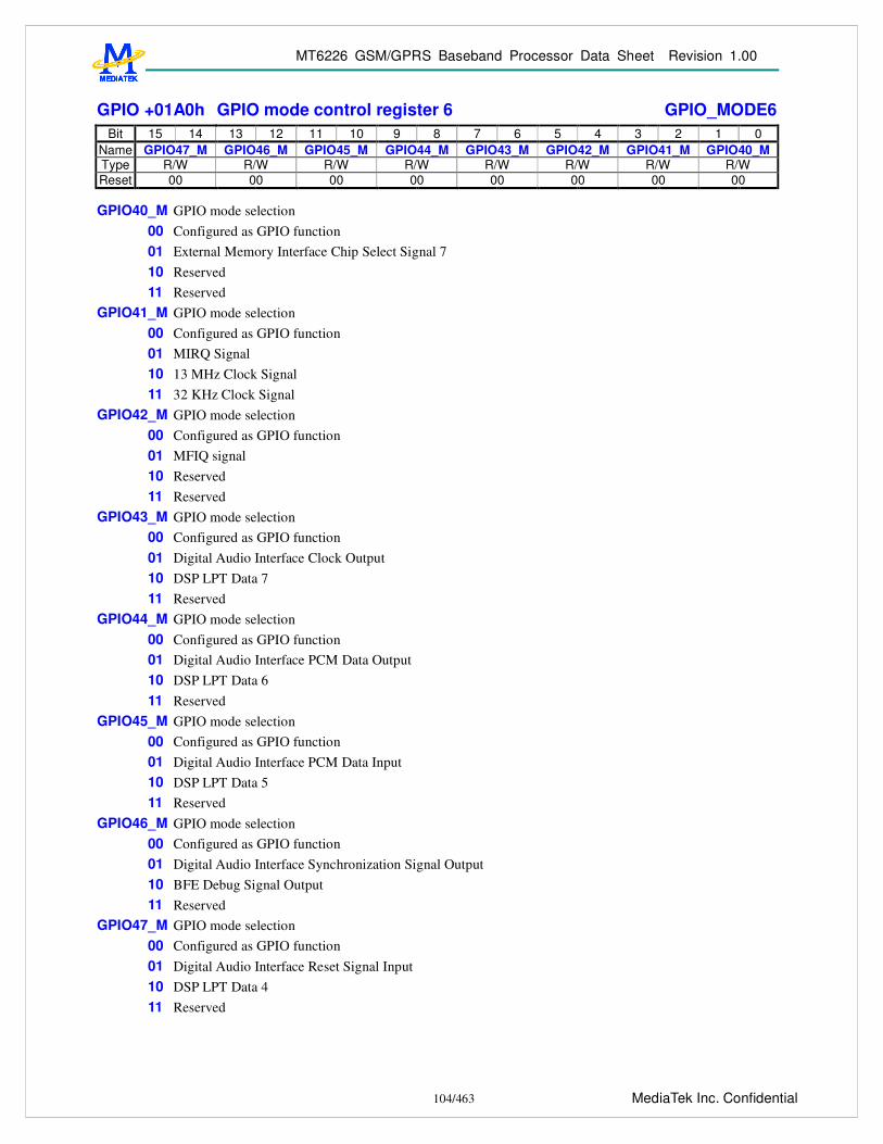
MT6226 GSM/GPRS Baseband Processor Data Sheet Revision 1.00
104/463 MediaTek Inc. Confidential
GPIO +01A0h GPIO mode control register 6 GPIO_MODE6 Bit 15 14 13 12 11 10 9 8 7 6 5 4 3 2 1 0
Name GPIO47_M GPIO46_M GPIO45_M GPIO44_M GPIO43_M GPIO42_M GPIO41_M GPIO40_M Type R/W R/W R/W R/W R/W R/W R/W R/W Reset 00 00 00 00 00 00 00 00
GPIO40_M GPIO mode selection
00 Configured as GPIO function 01 External Memory Interface Chip Select Signal 7 10 Reserved 11 Reserved
GPIO41_M GPIO mode selection 00 Configured as GPIO function 01 MIRQ Signal 10 13 MHz Clock Signal 11 32 KHz Clock Signal
GPIO42_M GPIO mode selection 00 Configured as GPIO function 01 MFIQ signal 10 Reserved 11 Reserved
GPIO43_M GPIO mode selection 00 Configured as GPIO function 01 Digital Audio Interface Clock Output 10 DSP LPT Data 7 11 Reserved
GPIO44_M GPIO mode selection 00 Configured as GPIO function 01 Digital Audio Interface PCM Data Output 10 DSP LPT Data 6 11 Reserved
GPIO45_M GPIO mode selection 00 Configured as GPIO function 01 Digital Audio Interface PCM Data Input 10 DSP LPT Data 5 11 Reserved
GPIO46_M GPIO mode selection 00 Configured as GPIO function 01 Digital Audio Interface Synchronization Signal Output 10 BFE Debug Signal Output 11 Reserved
GPIO47_M GPIO mode selection 00 Configured as GPIO function 01 Digital Audio Interface Reset Signal Input 10 DSP LPT Data 4 11 Reserved

MT6226 GSM/GPRS Baseband Processor Data Sheet Revision 1.00
105/463 MediaTek Inc. Confidential
GPIO +01B0h GPIO mode control register 7 GPIO_MODE7 Bit 15 14 13 12 11 10 9 8 7 6 5 4 3 2 1 0
Name GPIO55 GPIO54 GPIO53 GPIO52 GPIO51 GPIO50 GPIO49 GPIO48 Type R/W R/W R/W R/W R/W R/W R/W R/W Reset 0 0 0 0 0 0 0 0
GPIO48_M GPIO mode selection
00 Configured as GPIO function 01 CMOS Sensor Reset Signal Output 10 Reserved 11 Reserved
GPIO49_M GPIO mode selection 00 Configured as GPIO function 01 CMOS Sensor Power Down Signal Output 10 Reserved 11 Reserved
GPIO50_M GPIO mode selection 00 Configured as GPIO function 01 CMOS Sensor Data Input 1 10 MMC4.0 data 5 11 Reserved
GPIO51_M GPIO mode selection 00 Configured as GPIO function 01 CMOS Sensor Data Input 0 10 MMC4.0 data 4 11 Reserved
GPIO52_M GPIO mode selection 00 Configured as GPIO function 01 External Memory Interface Chip Select 6 10 Reserved 11 Reserved
GPIO53_M GPIO mode selection 00 Configured as GPIO function 01 External Memory Interface Chip Select 5 10 Reserved 11 Reserved
GPIO54_M GPIO mode selection 00 Configured as GPIO function 01 External Memory Interface Chip Select 4 10 Reserved 11 Reserved
GPIO55_M GPIO mode selection 00 Configured as GPIO function 01 NAND/LCD data 16 10 MMC4.0 data 6 11 DSP Task ID 0

MT6226 GSM/GPRS Baseband Processor Data Sheet Revision 1.00
106/463 MediaTek Inc. Confidential
GPIO +01D0h GPIO mode control register 8 GPIO_MODE8 Bit 15 14 13 12 11 10 9 8 7 6 5 4 3 2 1 0
Name GPIO56 Type R/W Reset 0
GPIO56_M GPIO mode selection
00 Configured as GPIO function 01 NAND/LCD data 17 10 MMC4.0 data 7 11 Reserved
GPIO +01C0h GPO mode control register 1 GPO_MODE1 Bit 15 14 13 12 11 10 9 8 7 6 5 4 3 2 1 0
Name GPO4_M GPO3_M GPO2_M GPO1_M GPO0_M Type R/W R/W R/W R/W R/W Reset 01 01 01 01 01
GPO0_M GPO mode selection
00 Configured as GPO function 01 VCXO Enable Signal Output Active High 10 Reserved 11 Reserved
GPO1_M GPO mode selection 00 Configured as GPO function 01 VCXO Enable Signal Output Active Low 10 Reserved 11 Reserved
GPO2_M GPO mode selection 00 Configured as GPO function 01 External Memory Interface Power Down Control for Pseudo SRAM 10 Reserved 11 Reserved
GPO3_M GPO mode selection 00 Configured as GPO function 01 External Memory Interface Address 24 10 Reserved 11 Reserved
GPO4_M GPO mode selection 00 Configured as GPO function 01 External Memory Interface Address25 10 Reserved 11 Reserved
GPIO+xxx4h GPIO xxx register SET GPIO_XXX_SET For all registers addresses listed above, writing to the +4h addresse offset will perform a bit-wise OR function between the 16bit written value and the 16bit register value already existing in the corresponding GPIO_xxx registers. Eg. If GPIO_DIR1 (GPIO+0000h) = 16’h0F0F,

MT6226 GSM/GPRS Baseband Processor Data Sheet Revision 1.00
107/463 MediaTek Inc. Confidential
writing GPIO_DIR1_SET (GPIO+0004h) = 16’F0F0 will result in GPIO_DIR1 = 16’hFFFF.
GPIO+xxx8h GPIO xxx register CLR GPIO_XXX_CLR For all registers addresses listed above, writing to the +8h addresse offset will perform a bit-wise AND-NOT function between the 16bit written value and the 16bit register value already existing in the corresponding GPIO_xxx registers. Eg. If GPIO_DIR1 (GPIO+0000h) = 16’h0F0F, writing GPIO_DIR1_CLR (GPIO+0008h) = 16’0F0F will result in GPIO_DIR1 = 16’h0000.
GPIO +0708h CAM/LCD I/O driving strength control ACIF_CON1 Bit 15 14 13 12 11 10 9 8 7 6 5 4 3 2 1 0
Name SLCD_SR
SLCD_E2
SLCD_E4
PLCD_SR
PLCD_E2
PLCD_E4
CAM_PD
CAM_SR
CAM_E2
CAM_E4
Type R/W R/W R/W R/W R/W R/W R/W R/W R/W R/W Reset 0 0 0 0 0 0 0 0 0 0
CAM_E4 The driving strength control of the sensor clock. CAM_E2 The driving strength control of the sensor clock. CAM_SR The slew rate control of the sensor clock. CAM_PD Pull-down control of the sensor interface, including pins CMVREF, CMHREF, and CMPCLK. PLCD _E4 The driving strength control of the parallel LCM control interface and NFI/LCM shared data bus. PLCD _E2 The driving strength control of the parallel LCM control interface and NFI/LCM shared data bus. PLCD_SR The slew rate control of the parallel LCM control interface and NFI/LCM shared data bus. SLCD_E4 The driving strength control of the serial LCM interface. SLCD _E2 The driving strength control of the serial LCM interface. SLCD _SR The slew rate control of the serial LCM interface.
4.6 General Purpose Timer
4.6.1 General Description Three general-purpose timers are provided. The timers are 16 bits long and run independently of each other, although they share the same clock source. Two timers can operate in one of two modes: one-shot mode and auto-repeat mode; the other is a free running timer. In one-shot mode, when the timer counts down and reaches zero, it is halted. In auto-repeat mode, when the timer reaches zero, it simply resets to countdown initial value and repeats the countdown to zero; this loop repeats until the disable signal is set to 1. Regardless of the timer’s mode, if the countdown initial value (i.e. GPTIMER1_DAT for GPT1 or GPTIMER_DAT2 for GPT2) is written when the timer is running, the new initial value does not take effect until the next time the timer is restarted. In auto-repeat mode, the new countdown start value is used on the next countdown iteration. Therefore, before enabling the gptimer, the desired values for GPTIMER_DAT and the GPTIMER_PRESCALER registers must first be set.
4.6.2 Register Definitions
GPT +0000h GPT1 Control register GPTIMER1_CO
N Bit 15 14 13 12 11 10 9 8 7 6 5 4 3 2 1 0
Name EN MODE Type R/W R/W Reset 0 0

MT6226 GSM/GPRS Baseband Processor Data Sheet Revision 1.00
108/463 MediaTek Inc. Confidential
MODE This register controls GPT1 to count repeatedly (in a loop) or just one-shot.
0 One-shot mode is selected. 1 Auto-repeat mode is selected.
EN This register controls GPT1 to start counting or to stop. 0 GPT1 is disabled. 1 GPT1 is enabled.
GPT +0004h GPT1 Time-Out Interval register GPTIMER1_DA
T Bit 15 14 13 12 11 10 9 8 7 6 5 4 3 2 1 0
Name CNT [15:0] Type R/W Reset FFFFh
CNT [15:0] Initial counting value. GPT1 counts down from GPTIMER1_DAT. When GPT1 counts down to zero,
a GPT1 interrupt is generated.
GPT +0008h GPT2 Control register GPTIMER2_CO
N Bit 15 14 13 12 11 10 9 8 7 6 5 4 3 2 1 0
Name EN MODE Type R/W R/W Reset 0 0
MODE This register controls GPT2 to count repeatedly (in a loop) or just one-shot.
0 One-shot mode is selected 1 Auto-repeat mode is selected
EN This register controls GPT2 to start counting or to stop. 0 GPT2 is disabled. 1 GPT2 is enabled.
GPT +000Ch GPT2 Time-Out Interval register GPTIMER2_DA
T Bit 15 14 13 12 11 10 9 8 7 6 5 4 3 2 1 0
Name CNT [15:0] Type R/W Reset FFFFh
CNT [15:0] Initial counting value. GPT2 counts down from GPTIMER2_DAT. When GPT2 counts down to zero,
a GPT2 interrupt is generated.
GPT +0010h GPT Status register GPTIMER_STA Bit 15 14 13 12 11 10 9 8 7 6 5 4 3 2 1 0
Name GPT2 GPT1 Type RC RC Reset 0 0
This register illustrates the gptimer timeout status. Each flag is set when the corresponding timer countdown completes, and can be cleared when the CPU reads the status register.

MT6226 GSM/GPRS Baseband Processor Data Sheet Revision 1.00
109/463 MediaTek Inc. Confidential
GPT +0014h GPT1 Prescaler register GPTIMER1_PRES
CALER Bit 15 14 13 12 11 10 9 8 7 6 5 4 3 2 1 0
Name PRESCALER [2:0] Type R/W Reset 100b
PRESCALER This register controls the counting clock for gptimer1.
000 16 KHz 001 8 KHz 010 4 KHz 011 2 KHz 100 1 KHz 101 500 Hz 110 250 Hz 111 125 Hz
GPT +0018h GPT2 Prescaler register GPTIMER2_PRES
CALER Bit 15 14 13 12 11 10 9 8 7 6 5 4 3 2 1 0
Name PRESCALER [2:0] Type R/W Reset 100b
PRESCALER This register controls the counting clock for gptimer2.
000 16 KHz 001 8 KHz 010 4 KHz 011 2 KHz 100 1 KHz 101 500 Hz 110 250 Hz 111 125 Hz
GPT+001Ch GPT3 Control register GPTIMER3_CO
N Bit 15 14 13 12 11 10 9 8 7 6 5 4 3 2 1 0
Name EN Type R/W Reset 0
EN This register controls GPT3 to start counting or to stop.
0 GPT3 is disabled. 1 GPT3 is enabled.
GPT+0020h GPT3 Time-Out Interval register GPTIMER3_DA
T Bit 15 14 13 12 11 10 9 8 7 6 5 4 3 2 1 0
Name CNT[15:0] Type RO Reset 0

MT6226 GSM/GPRS Baseband Processor Data Sheet Revision 1.00
110/463 MediaTek Inc. Confidential
CNT [15:0] If EN=1, GPT3 is a free running timer . Software reads this register for the countdown start value for
GPT3.
GPT+0024h GPT3 Prescaler register GPTIMER3_PRES
CALER Bit 15 14 13 12 11 10 9 8 7 6 5 4 3 2 1 0
Name PRESCALER [2:0] Type R/W Reset 100b
PRESCALER This register controls the counting clock for gptimer3.
000 16 KHz 001 8 KHz 010 4 KHz 011 2 KHz 100 1 KHz 101 500 Hz 110 250 Hz 112 125 Hz
4.7 UART
4.7.1 General Description The baseband chipset houses three UARTs. The UARTs provide full duplex serial communication channels between baseband chipset and external devices.
The UART has M16C450 and M16550A modes of operation, which are compatible with a range of standard software drivers. The extensions have been designed to be broadly software compatible with 16550A variants, but certain areas offer no consensus.
In common with the M16550A, the UART supports word lengths from five to eight bits, an optional parity bit and one or two stop bits, and is fully programmable by an 8-bit CPU interface. A 16-bit programmable baud rate generator and an 8-bit scratch register are included, together with separate transmit and receive FIFOs. Eight modem control lines and a diagnostic loop-back mode are provided. The UART also includes two DMA handshake lines, used to indicate when the FIFOs are ready to transfer data to the CPU. Interrupts can be generated from any of the 10 sources.
Note: The UART has been designed so that all internal operations are synchronized by the CLK signal. This synchronization results in minor timing differences between the UART and the industry standard 16550A device, which means that the core is not clock for clock identical to the original device.
After a hardware reset, the UART is in M16C450 mode. Its FIFOs can be enabled and the UART can then enter M16550A mode. The UART adds further functionality beyond M16550A mode. Each of the extended functions can be selected individually under software control.
The UART provides more powerful enhancements than the industry-standard 16550:
Hardware flow control. This feature is very useful when the ISR latency is hard to predict and control in the embedded applications. The MCU is relieved of having to fetch the received data within a fixed amount of time.

MT6226 GSM/GPRS Baseband Processor Data Sheet Revision 1.00
111/463 MediaTek Inc. Confidential
Output of an IR-compatible electrical pulse with a width 3/16 of that of a regular bit period.
Note: In order to enable any of the enhancements, the Enhanced Mode bit, EFR[4], must be set. If EFR[4] is not set, IER[7:5], FCR[5:4], ISR[5:4] and MCR[7:6] cannot be written. The Enhanced Mode bit ensures that the UART is backward compatible with software that has been written for 16C450 and 16550A devices.
Figure 67 shows the block diagram of the UART device.
APBBUSI/F
Baud RateGenerator
TX FIFO TX Machine
RX FIFO
ModemControl
RX Machine
Modem Outputs
Modem Inputs
APB Bus
clock
divisor
uart_tx_data
uart_rx_data
baud
Figure 67 Block Diagram of UART
4.7.2 Register Definitions n = 1, 2, 3; for uart1, uart2 and uart3 respectively.
UARTn+0000h RX Buffer Register UARTn_RBR Bit 15 14 13 12 11 10 9 8 7 6 5 4 3 2 1 0
Name RBR[7:0] Type RO
RBR RX Buffer Register. Read-only register. The received data can be read by accessing this register.
Modified when LCR[7] = 0.
UARTn+0000h TX Holding Register UARTn_THR Bit 15 14 13 12 11 10 9 8 7 6 5 4 3 2 1 0
Name THR[7:0] Type WO
THR TX Holding Register. Write-only register. The data to be transmitted is written to this register, and then
sent to the PC via serial communication. Modified when LCR[7] = 0.
UARTn+0004h Interrupt Enable Register UARTn_IER Bit 15 14 13 12 11 10 9 8 7 6 5 4 3 2 1 0
Name CTSI RTSI XOFFI X EDSSI ELSI ETBEI ERBFI Type R/W Reset 0
IER By storing a ‘1’ to a specific bit position, the interrupt associated with that bit is enabled. Otherwise, the
interrupt is disabled.

MT6226 GSM/GPRS Baseband Processor Data Sheet Revision 1.00
112/463 MediaTek Inc. Confidential
IER[3:0] are modified when LCR[7] = 0. IER[7:4] are modified when LCR[7] = 0 & EFR[4] = 1.
CTSI Masks an interrupt that is generated when a rising edge is detected on the CTS modem control line. Note: This interrupt is only enabled when hardware flow control is enabled. 0 Unmask an interrupt that is generated when a rising edge is detected on the CTS modem control line. 1 Mask an interrupt that is generated when a rising edge is detected on the CTS modem control line.
RTSI Masks an interrupt that is generated when a rising edge is detected on the RTS modem control line. Note: This interrupt is only enabled when hardware flow control is enabled. 0 Unmask an interrupt that is generated when a rising edge is detected on the RTS modem control line. 1 Mask an interrupt that is generated when a rising edge is detected on the RTS modem control line.
XOFFI Masks an interrupt that is generated when an XOFF character is received. Note: This interrupt is only enabled when software flow control is enabled. 0 Unmask an interrupt that is generated when an XOFF character is received. 1 Mask an interrupt that is generated when an XOFF character is received.
EDSSI When set ("1"), an interrupt is generated if DDCD, TERI, DDSR or DCTS (MSR[4:1]) becomes set. 0 No interrupt is generated if DDCD, TERI, DDSR or DCTS (MSR[4:1]) becomes set. 1 An interrupt is generated if DDCD, TERI, DDSR or DCTS (MSR[4:1]) becomes set.
ELSI When set ("1"), an interrupt is generated if BI, FE, PE or OE (LSR[4:1]) becomes set. 0 No interrupt is generated if BI, FE, PE or OE (LSR[4:1]) becomes set. 1 An interrupt is generated if BI, FE, PE or OE (LSR[4:1]) becomes set.
ETBEI When set ("1"), an interrupt is generated if the TX Holding Register is empty or the contents of the TX FIFO have been reduced to its Trigger Level.
0 No interrupt is generated if the TX Holding Register is empty or the contents of the TX FIFO have been reduced to its Trigger Level.
1 An interrupt is generated if the TX Holding Register is empty or the contents of the TX FIFO have been reduced to its Trigger Level
ERBFI When set ("1"), an interrupt is generated if the RX Buffer contains data. 0 No interrupt is generated if the RX Buffer contains data. 1 An interrupt is generated if the RX Buffer contains data.
UARTn+0008h Interrupt Identification Register UARTn_IIR Bit 15 14 13 12 11 10 9 8 7 6 5 4 3 2 1 0
Name FIFOE ID4 ID3 ID2 ID1 ID0 NINT Type RO Reset 0 0 0 0 0 0 0 1
IIR Identify if there are pending interrupts; ID4 and ID3 are presented only when EFR[4] = 1.
The following table gives the IIR[5:0] codes associated with the possible interrupts:
IIR[5:0] Priority Level
Interrupt Source
000001 - No interrupt pending 000110 1 Line Status Interrupt BI, FE, PE or OE set in LSR 000100 2 RX Data Received RX Data received or RX Trigger Level reached. 001100 2 RX Data Timeout Timeout on character in RX FIFO. 000010 3 TX Holding Register Empty TX Holding Register empty or TX FIFO Trigger Level reached. 000000 4 Modem Status change DDCD, TERI, DDSR or DCTS set in MSR 010000 5 Software Flow Control XOFF Character received 100000 6 Hardware Flow Control CTS or RTS Rising Edge

MT6226 GSM/GPRS Baseband Processor Data Sheet Revision 1.00
113/463 MediaTek Inc. Confidential
Table 25 The IIR[5:0] codes associated with the possible interrupts
Line Status Interrupt: A RX Line Status Interrupt (IIR[5:0 ] == 000110b) is generated if ELSI (IER[2]) is set and any of BI, FE, PE or OE (LSR[4:1]) becomes set. The interrupt is cleared by reading the Line Status Register.
RX Data Received Interrupt: A RX Received interrupt (IER[5:0] == 000100b) is generated if EFRBI (IER[0]) is set and either RX Data is placed in the RX Buffer Register or the RX Trigger Level is reached. The interrupt is cleared by reading the RX Buffer Register or the RX FIFO (if enabled).
RX Data Timeout Interrupt:
When virtual FIFO mode is disabled, RX Data Timeout Interrupt is generated if all of the following apply:
1. FIFO contains at least one character;
2. The most recent character was received longer than four character periods ago (including all start, parity and stop bits);
3. The most recent CPU read of the FIFO was longer than four character periods ago.
The timeout timer is restarted on receipt of a new byte from the RX Shift Register, or on a CPU read from the RX FIFO.
The RX Data Timeout Interrupt is enabled by setting EFRBI (IER[0]) to 1, and is cleared by reading RX FIFO.
When virtual FIFO mode is enabled, RX Data Timeout Interrupt is generated if all of the following apply:
1. FIFO is empty;
2. The most recent character was received longer than four character periods ago (including all start, parity and stop bits);
3. The most recent CPU read of the FIFO was longer than four character periods ago.
The timeout timer is restarted on receipt of a new byte from the RX Shift Register.
RX Holding Register Empty Interrupt: A TX Holding Register Empty Interrupt (IIR[5:0] = 000010b) is generated if ETRBI (IER[1]) is set and either the TX Holding Register or, if FIFOs are enabled, the TX FIFO becomes empty. The interrupt is cleared by writing to the TX Holding Register or TX FIFO if FIFO enabled.
Modem Status Change Interrupt: A Modem Status Change Interrupt (IIR[5:0] = 000000b) is generated if EDSSI (IER[3]) is set and either DDCD, TERI, DDSR or DCTS (MSR[3:0]) becomes set. The interrupt is cleared by reading the Modem Status Register.
Software Flow Control Interrupt: A Software Flow Control Interrupt (IIR[5:0] = 010000b) is generated if Software Flow Control is enabled and XOFFI (IER[5]) becomes set, indicating that an XOFF character has been received. The interrupt is cleared by reading the Interrupt Identification Register.
Hardware Flow Control Interrupt: A Hardware Flow Control Interrupt (IER[5:0] = 100000b) is generated if Hardware Flow Control is enabled and either RTSI (IER[6]) or CTSI (IER[7]) becomes set indicating that a rising edge has been detected on either the RTS/CTS Modem Control line. The interrupt is cleared by reading the Interrupt Identification Register.
UARTn+0008h FIFO Control Register UARTn_FCR Bit 15 14 13 12 11 10 9 8 7 6 5 4 3 2 1 0
Name RFTL1 RFTL0 TFTL1 TFTL0 DMA1 CLRT CLRR FIFOE Type WO
FCR FCR is used to control the trigger levels of the FIFOs, or flush the FIFOs.

MT6226 GSM/GPRS Baseband Processor Data Sheet Revision 1.00
114/463 MediaTek Inc. Confidential
FCR[7:6] is modified when LCR != BFh FCR[5:4] is modified when LCR != BFh & EFR[4] = 1
FCR[4:0] is modified when LCR != BFh FCR[7:6] RX FIFO trigger threshold
0 1 0 6 1 12 2 22
FCR[5:4] TX FIFO trigger threshold 0 1 1 4 2 8 3 14
DMA1 This bit determines the DMA mode, which the TXRDY and RXRDY pins support. TXRDY and RXRDY act to support single-byte transfers between the UART and memory (DMA mode 0) or multiple byte transfers (DMA mode1). Note that this bit has no effect unless the FIFOE bit is set as well 0 The device operates in DMA Mode 0. 1 The device operates in DMA Mode 1. TXRDY – mode0: Goes active (low) when the TX FIFO or the TX Holding Register is empty. Becomes
inactive when a byte is written to the Transmit channel. TXRDY – mode1: Goes active (low) when there are no characters in the TX FIFO. Becomes inactive when
the TX FIFO is full. RXRDY – mode0: Becomes active (low) when at least one character is in the RX FIFO or the RX Buffer
Register is full. Becomes inactive when there are no more characters in the RX FIFO or RX Buffer register.
RXRDY – mode1: Becomes active (low) when the RX FIFO Trigger Level is reached or an RX FIFO Character Timeout occurs. Goes inactive when the RX FIFO is empty.
CLRT Clear Transmit FIFO. This bit is self-clearing. 0 Leave TX FIFO intact. 1 Clear all the bytes in the TX FIFO.
CLRR Clear Receive FIFO. This bit is self-clearing. 0 Leave RX FIFO intact. 1 Clear all the bytes in the RX FIFO.
FIFOE FIFO Enabled. This bit must be set to 1 for any of the other bits in the registers to have any effect. 0 Disable both the RX and TX FIFOs. 1 Enable both the RX and TX FIFOs.
UARTn+000Ch Line Control Register UARTn_LCR Bit 15 14 13 12 11 10 9 8 7 6 5 4 3 2 1 0
Name DLAB SB SP EPS PEN STB WLS1 WLS0 Type R/W Reset 0 0 0 0 0 0 0 0
LCR Line Control Register. Determines characteristics of serial communication signals. Modified when LCR[7] = 0. DLAB Divisor Latch Access Bit.
0 The RX and TX Registers are read/written at Address 0 and the IER register is read/written at Address 4. 1 The Divisor Latch LS is read/written at Address 0 and the Divisor Latch MS is read/written at Address 4.
SB Set Break

MT6226 GSM/GPRS Baseband Processor Data Sheet Revision 1.00
115/463 MediaTek Inc. Confidential
0 No effect 1 SOUT signal is forced into the “0” state.
SP Stick Parity 0 No effect. 1 The Parity bit is forced into a defined state, depending on the states of EPS and PEN: If EPS=1 & PEN=1, the Parity bit is set and checked = 0.
If EPS=0 & PEN=1, the Parity bit is set and checked = 1. EPS Even Parity Select
0 When EPS=0, an odd number of ones is sent and checked. 1 When EPS=1, an even number of ones is sent and checked.
PEN Parity Enable 0 The Parity is neither transmitted nor checked. 1 The Parity is transmitted and checked.
STB Number of STOP bits 0 One STOP bit is always added. 1 Two STOP bits are added after each character is sent; unless the character length is 5 when 1 STOP bit is
added. WLS1, 0 Word Length Select.
0 5 bits 1 6 bits 2 7 bits 3 8 bits
UARTn+0010h Modem Control Register UARTn_MCR Bit 15 14 13 12 11 10 9 8 7 6 5 4 3 2 1 0
Name XOFF STAT
US
IR ENAB
LE X LOOP OUT2 OUT1 RTS DTR
Type R/W Reset 0 0 0 0 0 0 0 0
MCR Modem Control Register. Control interface signals of the UART.
MCR[4:0] are modified when LCR[7] = 0, MCR[7:6] are modified when LCR[7] = 0 & EFR[4] = 1.
XOFF Status This is a read-only bit. 0 When an XON character is received. 1 When an XOFF character is received.
IR Enable Enable IrDA modulation/demodulation. 0 Disable IrDA modulation/demodulation. 1 Enable IrDA modulation/demodulation.
LOOP Loop-back control bit. 0 No loop-back is enabled. 1 Loop-back mode is enabled.
OUT2 Controls the state of the output NOUT2, even in loop mode. 0 NOUT2=1. 1 NOUT2=0.
OUT1 Controls the state of the output NOUT1, even in loop mode. 0 NOUT1=1. 1 NOUT1=0.

MT6226 GSM/GPRS Baseband Processor Data Sheet Revision 1.00
116/463 MediaTek Inc. Confidential
RTS Controls the state of the output NRTS, even in loop mode. 0 NRTS=1. 1 NRTS=0.
DTR Control the state of the output NDTR, even in loop mode. 0 NDTR=1. 1 NDTR=0.
UARTn+0014h Line Status Register UARTn_LSR Bit 15 14 13 12 11 10 9 8 7 6 5 4 3 2 1 0
Name FIFOERR TEMT THRE BI FE PE OE DR
Type R/W Reset 0 1 1 0 0 0 0 0
LSR Line Status Register.
Modified when LCR[7] = 0. FIFOERR RX FIFO Error Indicator.
0 No PE, FE, BI set in the RX FIFO. 1 Set to 1 when there is at least one PE, FE or BI in the RX FIFO.
TEMT TX Holding Register (or TX FIFO) and the TX Shift Register are empty. 0 Empty conditions below are not met. 1 If FIFOs are enabled, the bit is set whenever the TX FIFO and the TX Shift Register are empty. If FIFOs
are disabled, the bit is set whenever TX Holding Register and TX Shift Register are empty. THRE Indicates if there is room for TX Holding Register or TX FIFO is reduced to its Trigger Level.
0 When at least one byte is written to the TX FIFO or the TX Shift Register. 1 Set whenever the contents of the TX FIFO are reduced to its Trigger Level (FIFOs are enabled), or
whenever TX Holding Register is empty and ready to accept new data (FIFOs are disabled). BI Break Interrupt.
0 Reset by the CPU reading this register 1 If the FIFOs are disabled, this bit is set whenever the SIN is held in the 0 state for more than one
transmission time (START bit + DATA bits + PARITY + STOP bits). If the FIFOs are enabled, this error is associated with a corresponding character in the FIFO and is flagged when this byte is at the top of the FIFO. When a break occurs, only one zero character is loaded into the FIFO: the next character transfer is enabled when SIN goes into the marking state and receives the next valid start bit.
FE Framing Error. 0 Reset by the CPU reading this register 1 If the FIFOs are disabled, this bit is set if the received data did not have a valid STOP bit. If the FIFOs
are enabled, the state of this bit is revealed when the byte it refers to is the next to be read. PE Parity Error
0 Reset by the CPU reading this register 1 If the FIFOs are disabled, this bit is set if the received data did not have a valid parity bit. If the FIFOs
are enabled, the state of this bit is revealed when the referred byte is the next to be read. OE Overrun Error.
0 Reset by the CPU reading this register. 1 If the FIFOs are disabled, this bit is set if the RX Buffer was not read by the CPU before new data from
the RX Shift Register overwrote the previous contents.

MT6226 GSM/GPRS Baseband Processor Data Sheet Revision 1.00
117/463 MediaTek Inc. Confidential
If the FIFOs are enabled, an overrun error occurs when the RX FIFO is full and the RX Shift Register becomes full. OE is set as soon as this happens. The character in the Shift Register is then overwritten, but not transferred to the FIFO.
DR Data Ready. 0 Cleared by the CPU reading the RX Buffer or by reading all the FIFO bytes. 1 Set by the RX Buffer becoming full or by a byte being transferred into the FIFO.
UARTn+0018h Modem Status Register UARTn_MSR Bit 15 14 13 12 11 10 9 8 7 6 5 4 3 2 1 0
Name DCD RI DSR CTS DDCD TERI DDSR DCTS Type R/W R/W R/W R/W R/W R/W R/W R/W Reset Input Input Input Input 0 0 0 0
Note: After a reset, D4-D7 are inputs. A modem status interrupt can be cleared by writing ‘0’ or set by writing ‘1’ to this register. D0-D3 can be written to.
Modified when LCR[7] = 0.
MSR Modem Status Register DCD Data Carry Detect. When Loop = "0", this value is the complement of the NDCD input signal.
When Loop = "1", this value is equal to the OUT2 bit in the Modem Control Register. RI Ring Indicator. When Loop = "0", this value is the complement of the NRI input signal.
When Loop = "1", this value is equal to the OUT1 bit in the Modem Control Register. DSR Data Set Ready When Loop = "0", this value is the complement of the NDSR input signal.
When Loop = "1", this value is equal to the DTR bit in the Modem Control Register.
CTS Clear To Send. When Loop = "0", this value is the complement of the NCTS input signal.
When Loop = "1", this value is equal to the RTS bit in the Modem Control Register. DDCD Delta Data Carry Detect.
0 The state of DCD has not changed since the Modem Status Register was last read 1 Set if the state of DCD has changed since the Modem Status Register was last read.
TERI Trailing Edge Ring Indicator 0 The NRI input does not change since this register was last read. 1 Set if the NRI input changes from “0” to “1” since this register was last read.
DDSR Delta Data Set Ready 0 Cleared if the state of DSR has not changed since this register was last read. 1 Set if the state of DSR has changed since this register was last read.
DCTS Delta Clear To Send 0 Cleared if the state of CTS has not changed since this register was last read. 1 Set if the state of CTS has changed since this register was last read.
UARTn+001Ch Scratch Register UARTn_SCR Bit 15 14 13 12 11 10 9 8 7 6 5 4 3 2 1 0
Name SCR[7:0] Type R/W

MT6226 GSM/GPRS Baseband Processor Data Sheet Revision 1.00
118/463 MediaTek Inc. Confidential
A general purpose read/write register. After reset, its value is un-defined.
Modified when LCR[7] = 0.
UARTn+0000h Divisor Latch (LS) UARTn_DLL Bit 15 14 13 12 11 10 9 8 7 6 5 4 3 2 1 0
Name DLL[7:0] Type R/W Reset 1
UARTn+0004h Divisor Latch (MS) UARTn_DLM Bit 15 14 13 12 11 10 9 8 7 6 5 4 3 2 1 0
Name DLL[7:0] Type R/W Reset 0
Note: DLL & DLM can only be updated if DLAB is set (“1”).. Note too that division by 1 generates a BAUD signal that is constantly high.
Modified when LCR[7] = 1.
The table below shows the divisor needed to generate a given baud rate from CLK inputs of 13, 26 MHz and 52 MHz. The effective clock enable generated is 16 x the required baud rate.
BAUD 13MHz 26MHz 52MHz 110 7386 14773 29545 300 2708 5417 10833 1200 677 1354 2708 2400 338 677 1354 4800 169 339 677 9600 85 169 339 19200 42 85 169 38400 21 42 85 57600 14 28 56 115200 6 14 28
Table 26 Divisor needed to generate a given baud rate
UARTn+0008h Enhanced Feature Register UARTn_EFR Bit 15 14 13 12 11 10 9 8 7 6 5 4 3 2 1 0
Name AUTO CTS
AUTO RTS D5 ENAB
LE -E SW FLOW CONT[3:0]
Type R/W R/W R/W R/W R/W Reset 0 0 0 0 0
*NOTE: Only when LCR=BF’h
Auto CTS Enables hardware transmission flow control 0 Disabled. 1 Enabled.
Auto RTS Enables hardware reception flow control 0 Disabled. 1 Enabled.

MT6226 GSM/GPRS Baseband Processor Data Sheet Revision 1.00
119/463 MediaTek Inc. Confidential
Enable-E Enable enhancement features. 0 Disabled. 1 Enabled.
CONT[3:0] Software flow control bits. 00xx No TX Flow Control 10xx Transmit XON1/XOFF1 as flow control bytes 01xx Transmit XON2/XOFF2 as flow control bytes 11xx Transmit XON1 & XON2 and XOFF1 & XOFF2 as flow control words xx00 No RX Flow Control xx10 Receive XON1/XOFF1 as flow control bytes xx01 Receive XON2/XOFF2 as flow control bytes xx11 Receive XON1 & XON2 and XOFF1 & XOFF2 as flow control words
UARTn+0010h XON1 UARTn_XON1 Bit 15 14 13 12 11 10 9 8 7 6 5 4 3 2 1 0
Name XON1[7:0] Type R/W Reset 0
UARTn+0014h XON2 UARTn_XON2 Bit 15 14 13 12 11 10 9 8 7 6 5 4 3 2 1 0
Name XON2[7:0] Type R/W Reset 0
UARTn+0018h XOFF1 UARTn_XOFF1 Bit 15 14 13 12 11 10 9 8 7 6 5 4 3 2 1 0
Name XOFF1[7:0] Type R/W Reset 0
UARTn+001Ch XOFF2 UARTn_XOFF2 Bit 15 14 13 12 11 10 9 8 7 6 5 4 3 2 1 0
Name XOFF2[7:0] Type R/W Reset 0
*Note: XON1, XON2, XOFF1, XOFF2 are valid only when LCR=BFh.
UARTn+0020h AUTOBAUD_EN UARTn_AUTOBAU
D_EN Bit 15 14 13 12 11 10 9 8 7 6 5 4 3 2 1 0
Name AUTO_EN
Type R/W Reset 0
AUTOBAUD_EN Auto-baud enable signal
0 Auto-baud function disable 1 Auto-baud function enable

MT6226 GSM/GPRS Baseband Processor Data Sheet Revision 1.00
120/463 MediaTek Inc. Confidential
UARTn+0024h HIGH SPEED UART UARTn_HIGHSPEED Bit 15 14 13 12 11 10 9 8 7 6 5 4 3 2 1 0
Name SPEED [1:0] Type R/W Reset 0
SPEED UART sample counter base
0 based on 16*baud_pulse, baud_rate = system clock frequency/16/DLH, DLL 1 based on 8*baud_pulse, baud_rate = system clock frequency/8/DLH, DLL 2 based on 4*baud_pulse, baud_rate = system clock frequency/4/DLH, DLL 3 based on sampe_count * baud_pulse, baud_rate = system clock frequency / sampe_count
The table below shows the divisor needed to generate a given baud rate from CLK inputs of 13M Hz based on different HIGHSPEED value.
BAUD HIGHSPEED = 0 HIGHSPEED = 1 HIGHSPEED = 2 110 7386 14773 29545
300 2708 7386 14773
1200 677 2708 7386
2400 338 677 2708
4800 169 338 677
9600 85 169 338
19200 42 85 169
38400 21 42 85
57600 14 21 42
115200 7 14 21
230400 * 7 14
460800 * * 7
921600 * * *
Table 27 Divisor needed to generate a given baud rate from 13MHz based on different HIGHSPEED value
The table below shows the divisor needed to generate a given baud rate from CLK inputs of 26 MHz based on different HIGHSPEED value.
BAUD HIGHSPEED = 0 HIGHSPEED = 1 HIGHSPEED = 2 110 14773 29545 59091
300 5417 14773 29545
1200 1354 5417 14773
2400 677 1354 5417
4800 339 677 1354
9600 169 339 667
19200 85 169 339
38400 42 85 169
57600 28 42 85
115200 14 28 42

MT6226 GSM/GPRS Baseband Processor Data Sheet Revision 1.00
121/463 MediaTek Inc. Confidential
230400 7 14 28
460800 * 7 14
921600 * * 7
Table 28 Divisor needed to generate a given baud rate from 26 MHz based on different HIGHSPEED value
The table below shows the divisor needed to generate a given baud rate from CLK inputs of 52MHz based on different HIGHSPEED value.
BAUD HIGHSPEED = 0 HIGHSPEED = 1 HIGHSPEED = 2
110 29545 59091 118182
300 10833 29545 59091
1200 2708 10833 29545
2400 1354 2708 10833
4800 677 1354 2708
9600 339 677 1354
19200 169 339 677
38400 85 169 339
57600 56 85 169
115200 28 56 85
230400 14 28 56
460800 7 14 28
921600 * 7 14
Table 29 Divisor needed to generate a given baud rate from 52 MHz based on different HIGHSPEED value
UARTn+0028h SAMPLE_COUNT UARTn_SAMPLE_COUN
T Bit 15 14 13 12 11 10 9 8 7 6 5 4 3 2 1 0
Name SAMPLECOUNT [7:0] Type R/W Reset 0
When HIGHSPEED=3, the sample_count is the threshold value for UART sample counter (sample_num).
UARTn+002Ch
SAMPLE_POINT UARTn_SAMPLE_POIN
T Bit 15 14 13 12 11 10 9 8 7 6 5 4 3 2 1 0
Name SAMPLEPOINT [7:0] Type R/W Reset ffh
When HIGHSPEED=3, UART gets the input data when sample_count=sample_num. e.g. system clock = 13MHz, 921600 = 13000000 / 14 sample_count = 14 and sample point = 7 (sample the central point to decrease the inaccuracy)

MT6226 GSM/GPRS Baseband Processor Data Sheet Revision 1.00
122/463 MediaTek Inc. Confidential
UARTn+0030h AUTOBAUD_REG UARTn_AUTOBAUD_RE
G Bit 15 14 13 12 11 10 9 8 7 6 5 4 3 2 1 0
Name BAUD_STAT[3:0] BAUDRATE[3:0] Type RO RO Reset 0 0
BAUD_RATE Autobaud baud rate
0 115200 1 57600 2 38400 3 19200 4 9600 5 4800 6 2400 7 1200 8 300 9 110
BAUDSTAT Autobaud format 0 Autobaud is detecting 1 AT_7N1 2 AT_7O1 3 AT_7E1 4 AT_8N1 5 AT_8O1 6 AT_8E1 7 at_7N1 8 at_7E1 9 at_7O1 10 at_8N1 11 at_8E1 12 at_8O1 13 Autobaud detection fails
UARTn+0038h AUTOBAUDSAMPLE UARTn_AUTOBAUDSA
MPLE Bit 15 14 13 12 11 10 9 8 7 6 5 4 3 2 1 0
Name AUTOBAUDSAMPLE Type R/W R/W R/W R/W R/W R/W R/W Reset dh
Since the system clock may change, autobaud sample duration should change as system clock changes. When system clock = 13MHz, autobaudsample = 6; when system clock = 26MHz, autobaudsample = 13.
UARTn+003Ch
Guard time added register UARTn_GUARD
Bit 15 14 13 12 11 10 9 8 7 6 5 4 3 2 1 0
Name GUARD_
EN GUARD_CNT[3:0]
Type R/W R/W R/W R/W R/W

MT6226 GSM/GPRS Baseband Processor Data Sheet Revision 1.00
123/463 MediaTek Inc. Confidential
Reset 0 0 0 0 0
GUARD_CNT Guard interval count value. Guard interval = (1/(system clock / 16 / div )) * GUARD_CNT. GUARD_EN Guard interval add enable signal.
0 No guard interval added. 1 Add guard interval after stop bit.
UARTn+0040h Escape character register UARTn_ESCAPE_DAT Bit 15 14 13 12 11 10 9 8 7 6 5 4 3 2 1 0
Name ESCAPE_DAT[7:0] Type R/W Reset FFh
ESCAPE_DAT Escape character added before software flow control data and escape character, i.e. if tx data is xon
(31h), with esc_en =1, uart transmits data as esc + CEh (~xon).
UARTn+0044h Escape enable register UARTn_ESCAPE_EN Bit 15 14 13 12 11 10 9 8 7 6 5 4 3 2 1 0
Name ESC_EN
Type R/W Reset 0
ESC_EN Add escape character in transmitter and remove escape character in receiver by UART.
0 Do not deal with the escape character. 1 Add escape character in transmitter and remove escape character in receiver.
UARTn+0048h Sleep enable register UARTn_SLEEP_EN Bit 15 14 13 12 11 10 9 8 7 6 5 4 3 2 1 0
Name SELLP_EN
Type R/W Reset 0
SLEEP_EN For sleep mode issue
0 Do not deal with sleep mode indicate signal 1 To activate hardware flow control or software control according to software initial setting when chip
enters sleep mode. Releasing hardware flow when chip wakes up; but for software control, uart sends xon when awaken and when FIFO does not reach threshold level.
UARTn+004Ch
Virtual FIFO enable register UARTn_VFIFO_EN
Bit 15 14 13 12 11 10 9 8 7 6 5 4 3 2 1 0
Name VFIFO_EN
Type R/W Reset 0
VFIFO_EN Virtual FIFO mechanism enable signal.
0 Disable VFIFO mode. 1 Enable VFIFO mode. When virtual mode is enabled, the flow control is based on the DMA threshold,
and generates a timeout interrupt for DMA.

MT6226 GSM/GPRS Baseband Processor Data Sheet Revision 1.00
124/463 MediaTek Inc. Confidential
4.8 IrDA Framer
4.8.1 General Description IrDA framer, which is depicted in Figure 68, is implemented to reduce the CPU loading for IrDA transmission. IrDA framer functional block can be divided into two parts: the transmitting part and the receiving part. In the transmitter, it will perform BOFs addition, byte stuffing, the addition of 16-bits FCS, and EOF appendence. In the receiving part, it will execute BOFs removal, ESC character removal, CRC checking, and EOF detection. In addition, the framer will perform 3/16 modulation and demodulation to connect to the IR transceiver. The transmitter and receiver all need DMA channel.
Figure 68 IrDA framer functional block
4.8.2 Register Definitions
IRDA+0000h TX BUF and RX BUF BUF Bit 15 14 13 12 11 10 9 8 7 6 5 4 3 2 1 0
Name BUF[7:0] Type R/W Reset 0
BUF IrDA Framer transmit or receive data
IRDA+0004h TX BUF and RX BUF clear signal BUF_CLEAR Bit 15 14 13 12 11 10 9 8 7 6 5 4 3 2 1 0
Name CLEAR Type R/W Reset 0
CLEAR When CLEAR=1, the FIFO will be cleared
IRDA+0008h Maximum Turn Around Time MAX_T Bit 15 14 13 12 11 10 9 8 7 6 5 4 3 2 1 0
Name MAX_T [13:0] Type R/W Reset 3E80h
MAX_T Maximum turn around time is the maximum time that a station can hold the P/F bit. This parameter along with
the baud rate parameter dictates the maximum number of bytes that a station can transmit before giving the line to another station by transmitting a frame with the P/F bit. This parameter is used by one station to

MT6226 GSM/GPRS Baseband Processor Data Sheet Revision 1.00
125/463 MediaTek Inc. Confidential
indicate the maximum time the other station can send before it must turn the link around. 500ms is the only valid value when the baud rate is less than 115200kbps. The default value is 500ms.
IRDA+000Ch Minimum Turn Around Time MIN_T Bit 15 14 13 12 11 10 9 8 7 6 5 4 3 2 1 0
Name MIN_T [15:0] Type R/W Reset FDE8h
MIN_T Minimum turn around time, the default value is 10ms. The minimum turn around time parameter deals with the
time needed for a receiver to recover following saturation by transmission from the same device. This parameter corresponds to the required time delay between the last byte of the last frame sent by a station and the point at which it is ready to receive the first byte of a frame from another station, i.e. it is the latency for transmit to complete and be ready for receive.
IRDA+0010h Number of additional BOFs prefixed to the beginning of a frame
BOFS
Bit 15 14 13 12 11 10 9 8 7 6 5 4 3 2 1 0 Name TYPE BOFS [6:0] Type R/W R/W Reset 0 1011b
BOFs Additional BOFs number; the additional BOFs parameter indicates the number of additional flags needed at the
beginning of every frame. The main purpose of the addition of additional BOFs is to provide a delay at the beginning of each frame for device with long interrupt latency.
TYPE Additional BOFs type 1 BOF = C0h 0 BOF = FFh
IRDA+0014h Baud rate divisor DIV Bit 15 14 13 12 11 10 9 8 7 6 5 4 3 2 1 0
Name DIV[15:0] Type R/W Reset 55h
DIV Transmit or receive rate divider. Rate = System clock frequency / DIV/ 16; the default value = ‘h55 when in
contention mode.
IRDA+0018h Transmit frame size TX_FRAME_SIZ
E Bit 15 14 13 12 11 10 9 8 7 6 5 4 3 2 1 0
Name TX_FRAME_SIZE[11:0] Type R/W Reset 40h
TX_FRAME_SIZE Transmit frame size; the default value = 64 when in contention mode.
IRDA+001Ch Receiving frame1 size RX_FRAME1_SI
ZE Bit 15 14 13 12 11 10 9 8 7 6 5 4 3 2 1 0
Name RX_FRAME1_SIZE[11:0] Type RO Reset 0

MT6226 GSM/GPRS Baseband Processor Data Sheet Revision 1.00
126/463 MediaTek Inc. Confidential
RX_FRAME1_SIZE The actual number of receiving frame1 size.
IRDA+0020h Transmit abort indication ABORT Bit 15 14 13 12 11 10 9 8 7 6 5 4 3 2 1 0
Name ABORT
Type R/W Reset 0
ABORT When set 1, the framer will transmit abort sequence and closes the frame without an FCS field or an ending
flag.
IRDA+0024h IrDA framer transmit enable signal TX_EN Bit 15 14 13 12 11 10 9 8 7 6 5 4 3 2 1 0
Name TX_ONE
TXINVERT
MODE TX_EN
Type R/W R/W R/W R/W Reset 0 0 0 0
TX_EN Transmit enable MODE Modulation type selection
0 3/16 modulation 1 1.61us
TXINVERT Invert transmit signal 0 transmit signal is not inverted 1 inverts transmit signal
TX_ONE: Control the tranmit enable signal is one hot or not 0 tx_en will not be de-asserted until software programs 1 tx_en will be de-asserted (i.e. transmit disabled) automatically after one frame has been sent
IRDA+0028h IrDA framer receive enable signal RX_EN Bit 15 14 13 12 11 10 9 8 7 6 5 4 3 2 1 0
Name RX_ONE
RXINVERT
RX_EN
Type R/W R/W R/W Reset 0 0 0
RX_EN Receive enable RXINVERT Invert receive signal
0 receive signal is not inverted 1 inverts receive signal
RX_ONE Disable receive when get one frame 0 rx_en will not be de-asserted until software programs 1 rx_en will be de-asserted (i.e. transmit disabled) automatically after one frame has been sent
IRDA+002Ch FIFO trigger level indication TRIGGER Bit 15 14 13 12 11 10 9 8 7 6 5 4 3 2 1 0
Name RX_TRIG[ TX_TRIG Type R/W R/W Reset 0 0
TX_TRIG The tx FIFO interrupt trigger threshold 00 0 byte 01 1 byte

MT6226 GSM/GPRS Baseband Processor Data Sheet Revision 1.00
127/463 MediaTek Inc. Confidential
02 2 byte RX_TRIG The rx FIFO interrupt trigger threshold 00 1 byte 01 2 byte 02 3 byte
IRDA+0030h IRQ enable signal IRQ_ENABLE Bit 15 14 13 12 11 10 9 8 7 6 5 4 3 2 1 0
Name 2NDRX_CO
MP
RXRESTART
THRESHTIMEOUT
FIFOTIMEOU
T
TXABORT
RXABORT
MAXTIMEOU
T
MINTIMEOU
T
RXCOMPLET
E
TXCOMPLET
E
STATUS
RXTRIG
TXTRIG
Type R/W R/W R/W R/W R/W R/W R/W R/W R/W R/W R/W R/W Reset 0 0 0 0 0 0 0 0 0 0 0 0
IRQ_ENABLE Interrupt enable signal
0 disable 1 enable
TXTRIG Transmit data reaches the threshold level 0 No interrupt is generated 1 Interrupt is generated when transmit FIFO size reaches threshold
RXTRIG Receive data reaches the threshold level 0 No interrupt is generated 1 Interrupt is generated when receive FIFO size reaches threshold
STATUS Any status lists as following has happened (overrun, size_error)
0 No interrupt is generated 1 Interrupt is generated when one of the statuses occurred
TXCOMPLETE Transmit one frame completely 0 No interrupt is generated 1 Interrupt is generated when transmitting one frame completely
RXCOMPLETE Receive one frame completely 0 No interrupt is generated 1 Interrupt is generated when receiving one frame completely
MINTIMEOUT Minimum time timeout 0 No interrupt is generated 1 Interrupt is generated when minimum timer is timed out
MAXTIMEOUT Maximum time timeout 0 No interrupt is generated 1 Interrupt is generated when maximum timer is timed out
RXABORT Receiving aborting frame 0 No interrupt is generated 1 Interrupt is generated when receiving aborting frame
TXABORT Transmitting aborting frame 0 No interrupt is generated 1 Interrupt is generated when transmitting aborting frame
FIFOTIMEOUT FIFO timeout 0 No interrupt is generated 1 Interrupt is generated when FIFO timeout
THRESHTIMEOUT Threshold time timeout

MT6226 GSM/GPRS Baseband Processor Data Sheet Revision 1.00
128/463 MediaTek Inc. Confidential
0 No interrupt is generated 1 Interrupt is generated when threshold timer is timed out
RXRESTART Receiving a new frame before one frame is received completely 0 No interrupt is generated 1 Interrupt is generated when receiving a new frame before one frame is received completely
2NDRX_COMP Receiving second frame and get P/F bit 0 No interrupt is generated
1 Interrupt is generated when receiving second frame and get P/F bit completely
IRDA+0034h Interrupt Status IRQ_STA Bit 15 14 13 12 11 10 9 8 7 6 5 4 3 2 1 0
Name 2NDRX_CO
MP
RXRESTART
THRESHTIMEOUT
FIFOTIMEOU
T
TXABORT
RXABORT
MAXTIMEOU
T
MINTIMEOU
T
RXCOMPLET
E
TXCOMPLET
E
STATUS
RXFIFO
TXFIFO
Type RC RC RC RC RC RC RC RC RC RC RC RC RC Reset 0 0 0 0 0 0 0 0 0 0 0 0 0
TXFIFO Transmit FIFO reaches threshold RXFIFO Receive FIFO reaches threshold ERROR generated when one of the statuses occurred
(data_error, PF_detect, fifo_hold1, fifo_empty, crc_fail, frame_error, overrun, size_error) TXCOMPLETE Transmitting one frame completely RXCOMPLETE Receiving one frame completely MINTIMEOUT Minimum turn around time timeout MAXTIMEOUT Maximum turn around time timeout RXABORT Receiving aborting frame TXABORT Transmitting aborting frame FIFOTIMEOUT FIFO is timeout THRESHTIMEOUT Threshold time timeout RXRESTART Receiving a new frame before one frame is received completely 2NDRX_COMP Receiving second frame and get P/F bit completely
IRDA+0038h STATUS register STATUS Bit 15 14 13 12 11 10 9 8 7 6 5 4 3 2 1 0
Name FIFOHO
LD1 FIFO
EMPTY OVERRUN
RXSIZE
Type R/W R/W R/W R/W Reset 0 0 0 0
RXSIZE Receive frame size error OVERRUN Frame over run FIFOEMPTY FIFO empty FIFOHOLD1 FIFO holds one
IRDA+003Ch Transceiver power on/off control TRANSCEIVER
_PDN Bit 15 14 13 12 11 10 9 8 7 6 5 4 3 2 1 0
Name TRANS_
PDN
Type R/W Reset 1
Transceiver_PDN Power on/off control for external IrDA transceiver

MT6226 GSM/GPRS Baseband Processor Data Sheet Revision 1.00
129/463 MediaTek Inc. Confidential
IRDA+0040h Maximum number of receiving frame size RX_FRAME_MA
X Bit 15 14 13 12 11 10 9 8 7 6 5 4 3 2 1 0
Name MAX_RX_FRAME_SIZE_ Type R/W Reset 0
RX_FRAME_MAX Receive frame max size, when actual receiving frame size is larger than rx_frame_max,
RXSIZE is asserted.
IRDA+0044h Threshold Time THRESH_T Bit 15 14 13 12 11 10 9 8 7 6 5 4 3 2 1 0
Name DISCONNECT_TIME[15:0] Type R/W Reset bb8h
THRESHOLD TIME Threshold time; it’s used to control the time a station will wait without receiving valid frame
before it disconnects the link. Associated with this is the time a station will wait without receiving valid frames before it will send a status indication to the service user layer.
IRDA+0048h Counter enable signal COUNT_ENABL
E Bit 15 14 13 12 11 10 9 8 7 6 5 4 3 2 1 0
Name THRESH
_EN
MIN_EN
MAX_EN
Type R/W R/W R/W Reset 0 0 0
COUNT_ENABLE Counter enable signals
IRDA+004Ch Indication of system clock rate CLOCK_RATE Bit 15 14 13 12 11 10 9 8 7 6 5 4 3 2 1 0
Name CLOCK_RATE
Type R/W Reset 0
CLOCK_RATE Indication of the system clock rate
0 26MHz 1 52MHz 2 13MHz
IRDA+0050h System Clock Rate Fix RATE_FIX Bit 15 14 13 12 11 10 9 8 7 6 5 4 3 2 1 0
Name RATE_FIX
Type R/W Reset 0
RATE_FIX Fix irda framer sample base clock rate as 13MHz
0 clock rate base on clock_rate selection 1 13MHz
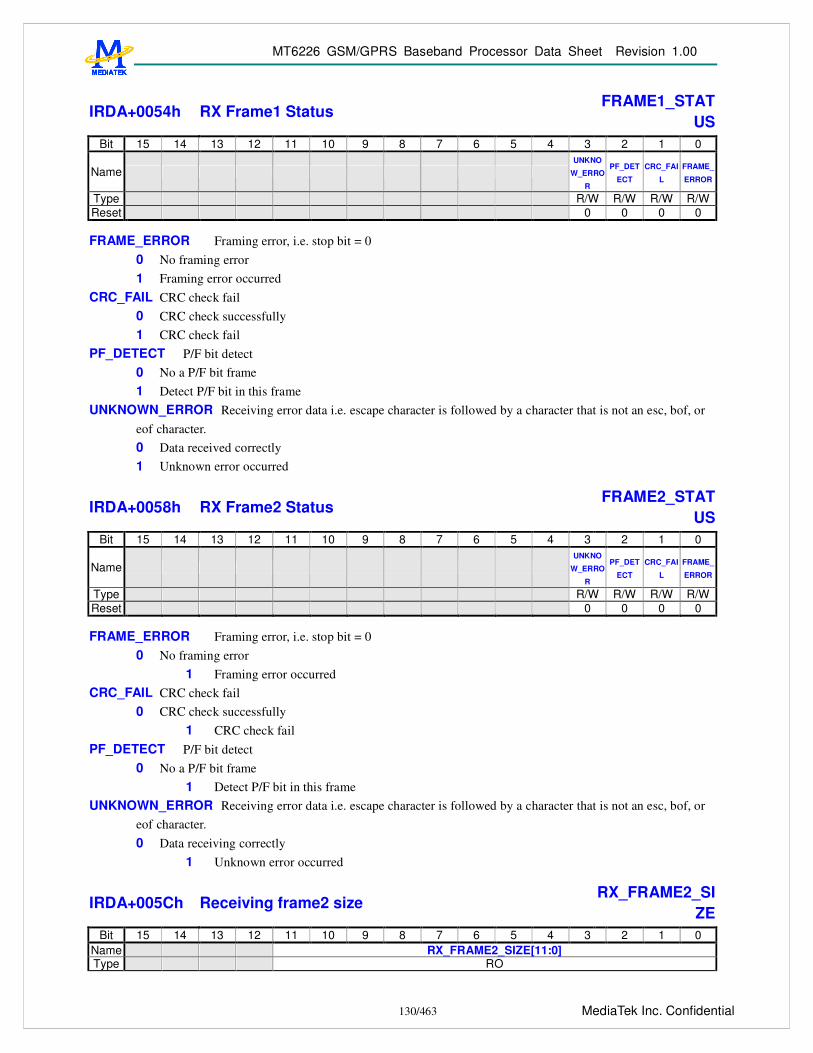
MT6226 GSM/GPRS Baseband Processor Data Sheet Revision 1.00
130/463 MediaTek Inc. Confidential
IRDA+0054h RX Frame1 Status FRAME1_STAT
US Bit 15 14 13 12 11 10 9 8 7 6 5 4 3 2 1 0
Name UNKNO
W_ERRO
R
PF_DET
ECT
CRC_FAI
L
FRAME_
ERROR
Type R/W R/W R/W R/W Reset 0 0 0 0
FRAME_ERROR Framing error, i.e. stop bit = 0
0 No framing error 1 Framing error occurred
CRC_FAIL CRC check fail 0 CRC check successfully 1 CRC check fail
PF_DETECT P/F bit detect 0 No a P/F bit frame 1 Detect P/F bit in this frame
UNKNOWN_ERROR Receiving error data i.e. escape character is followed by a character that is not an esc, bof, or eof character. 0 Data received correctly 1 Unknown error occurred
IRDA+0058h RX Frame2 Status FRAME2_STAT
US Bit 15 14 13 12 11 10 9 8 7 6 5 4 3 2 1 0
Name UNKNO
W_ERRO
R
PF_DET
ECT
CRC_FAI
L
FRAME_
ERROR
Type R/W R/W R/W R/W Reset 0 0 0 0
FRAME_ERROR Framing error, i.e. stop bit = 0
0 No framing error 1 Framing error occurred
CRC_FAIL CRC check fail 0 CRC check successfully
1 CRC check fail PF_DETECT P/F bit detect
0 No a P/F bit frame 1 Detect P/F bit in this frame
UNKNOWN_ERROR Receiving error data i.e. escape character is followed by a character that is not an esc, bof, or eof character. 0 Data receiving correctly
1 Unknown error occurred
IRDA+005Ch Receiving frame2 size RX_FRAME2_SI
ZE Bit 15 14 13 12 11 10 9 8 7 6 5 4 3 2 1 0
Name RX_FRAME2_SIZE[11:0] Type RO

MT6226 GSM/GPRS Baseband Processor Data Sheet Revision 1.00
131/463 MediaTek Inc. Confidential
Reset 0
RX_FRAME2_SIZE The actual number of receiving frame2 size.
4.9 Real Time Clock
4.9.1 General Description The Real Time Clock (RTC) module provides time and data information. The clock is based on a 32.768KHz oscillator with an independent power supply. When the mobile handset is powered off, a dedicated regulator supplies the RTC block. If the main battery is not present, a backup supply such as a small mercury cell battery or a large capacitor is used. In addition to providing timing data, an alarm interrupt is generated and can be used to power up the baseband core via the BBWAKEUP pin. Regulator interrupts corresponding to seconds, minutes, hours and days can be generated whenever the time counter value reaches a maximum value (e.g., 59 for seconds and minutes, 23 for hours, etc.). The year span is supported up to 2127. The maximum day-of-month values, which depend on the leap year condition, are stored in the RTC block.
4.9.2 Register Definitions
RTC+0000h Baseband power up RTC_BBPU Bit 15 14 13 12 11 10 9 8 7 6 5 4 3 2 1 0
Name KEY_BBPU AUTO BBPU WRITE_E
N
PWREN
Type W R/W R/W R/W R/W
KEY_BBPU A bus write is acceptable only when KEY_BBPU=0x43. AUTO Controls if BBWAKEUP is automatically in the low state when SYSRST# transitions from high to low.
0 BBWAKEUP is not automatically in the low state when SYSRST# transitions from high to low. 1 BBWAKEUP is automatically in the low state when SYSRST# transitions from high to low.
BBPU Controls the power of PMIC. If powerkey1=A357h and powerkey2=67D2h, PMIC takes on the value programmed by software; otherwise PMIC is low. 0 Power down
1 Power on WRITE_EN When WRITE_EN is set to 0 by the software program, the RTC write interface is disabled until another
system power on. PWREN
0 RTC alarm has no action on power switch. 1 When an RTC alarm occurs, BBPU is set to 1, and the system powers on by RTC alarm wakeup.
RTC+0004h RTC IRQ status RTC_IRQ_STA Bit 15 14 13 12 11 10 9 8 7 6 5 4 3 2 1 0
Name TCSTA
ALSTA
Type R/C R/C
ALSTA This register indicates the IRQ status and whether or not the alarm condition has been met. 0 No IRQ occurred; the alarm condition has not been met. 1 IRQ occurred; the alarm condition has been met.
TCSTA This register indicates the IRQ status and whether or not the tick condition has been met. 0 No IRQ occurred; the tick condition has not been met. 1 IRQ occurred; the tick condition has been met.

MT6226 GSM/GPRS Baseband Processor Data Sheet Revision 1.00
132/463 MediaTek Inc. Confidential
RTC+0008h RTC IRQ enable RTC_IRQ_EN Bit 15 14 13 12 11 10 9 8 7 6 5 4 3 2 1 0
Name WING ONESHOT
TC_EN
AL_EN
Type R/O R/W R/W R/W
ONESHOT Controls automatic reset of AL_EN and TC_EN. AL_EN This register enables the control bit for IRQ generation if the alarm condition has been met.
0 Disable IRQ generation. 1 Enable the alarm time match interrupt. Clear the interrupt when ONESHOT is high upon generation of
the corresponding IRQ. TC_EN This register enables the control bit for IRQ generation if the tick condition has been met.
0 Disable IRQ generation. 1 Enable the tick time match interrupt. Clear the interrupt when ONESHOT is high upon generation of the
corresponding IRQ. WING This bit indicates that RTC is still writing to this register.
RTC+000Ch Counter increment IRQ enable RTC_CII_EN Bit 15 14 13 12 11 10 9 8 7 6 5 4 3 2 1 0
Name WING 1/8SECCII
1/4SECCII
1/2SECCII
YEACII
MTHCII
DOWCII
DOMCII
HOUCII
MINCII
SECCII
Type R/O R/W R/W R/W R/W R/W R/W R/W R/W R/W R/W
This register activates or de-activates the IRQ generation when the TC counter reaches its maximum value.
SECCII Set this bit to 1 to activate the IRQ at each second update. MINCII Set the bit to 1 to activate the IRQ at each minute update. HOUCII Set the bit to 1 to activate the IRQ at each hour update. DOMCII Set the bit to 1 to activate the IRQ at each day-of-month update. DOWCII Set the bit to 1 to activate the IRQ at each day-of-week update. MTHCII Set the bit to 1 to activate the IRQ at each month update. YEACII Set the bit to 1 to activate the IRQ at each year update. 1/2SECCII Set the bit to 1 to activate the IRQ at each one-half of a second update. 1/4SECCII Set the bit to 1 to activate the IRQ at each one-fourth of a second update. 1/8SECCII Set the bit to 1 to activate the IRQ at each one-eighth of a second update. WING This bit indicates RTC is still writing to this register.
RTC+0010h RTC alarm mask RTC_AL_MASK Bit 15 14 13 12 11 10 9 8 7 6 5 4 3 2 1 0
Name WING YEA_MSK
MTH_MSK
DOW_MSK
DOM_MSK
HOU_MSK
MIN_MSK
SEC_MSK
Type R/O R/W R/W R/W R/W R/W R/W R/W
The alarm condition for alarm IRQ generation depends on whether or not the corresponding bit in this register is masked.
SEC_MSK 0 Condition (RTC_TC_SEC = RTC_AL_SEC) is checked to generate the alarm signal. 1 Condition (RTC_TC_SEC = RTC_AL_SEC) is masked, i.e. the value of RTC_TC_SEC does not affect
the alarm IRQ generation. MIN_MSK
0 Condition (RTC_TC_MIN = RTC_AL_MIN) is checked to generate the alarm signal.

MT6226 GSM/GPRS Baseband Processor Data Sheet Revision 1.00
133/463 MediaTek Inc. Confidential
1 Condition (RTC_TC_MIN = RTC_AL_MIN) is masked, i.e. the value of RTC_TC_MIN does not affect the alarm IRQ generation.
HOU_MSK 0 Condition (RTC_TC_HOU = RTC_AL_HOU) is checked to generate the alarm signal. 1 Condition (RTC_TC_HOU = RTC_AL_HOU) is masked, i.e. the value of RTC_TC_HOU does not affect
the alarm IRQ generation. DOM_MSK
0 Condition (RTC_TC_DOM = RTC_AL_DOM) is checked to generate the alarm signal. 1 Condition (RTC_TC_DOM = RTC_AL_DOM) is masked, i.e. the value of RTC_TC_DOM does not
affect the alarm IRQ generation. DOW_MSK
0 Condition (RTC_TC_DOW = RTC_AL_DOW) is checked to generate the alarm signal. 1 Condition (RTC_TC_DOW = RTC_AL_DOW) is masked, i.e. the value of RTC_TC_DOW does not
affect the alarm IRQ generation. MTH_MSK
0 Condition (RTC_TC_MTH = RTC_AL_MTH) is checked to generate the alarm signal. 1 Condition (RTC_TC_MTH = RTC_AL_MTH) is masked, i.e. the value of RTC_TC_MTH does not affect
the alarm IRQ generation. YEA_MSK
0 Condition (RTC_TC_YEA = RTC_AL_YEA) is checked to generate the alarm signal. 1 Condition (RTC_TC_YEA = RTC_AL_YEA) is masked, i.e. the value of RTC_TC_YEA does
not affect the alarm IRQ generation. WING This bit indicates RTC is still writing to this register.
RTC+0014h RTC seconds time counter register RTC_TC_SEC Bit 15 14 13 12 11 10 9 8 7 6 5 4 3 2 1 0
Name WING TC_SECOND Type R/O R/W
TC_SECOND The second initial value for the time counter. The range of its value is: 0-59. WING This bit indicates RTC is still writing to this register.
RTC+0018h RTC minutes time counter register RTC_TC_MIN Bit 15 14 13 12 11 10 9 8 7 6 5 4 3 2 1 0
Name WING TC_MINUTE Type R/O R/W
TC_MINUTE The minute initial value for the time counter. The range of its value is: 0-59. WING This bit indicates RTC is still writing to this register.
RTC+001Ch RTC hours time counter register RTC_TC_HOU Bit 15 14 13 12 11 10 9 8 7 6 5 4 3 2 1 0
Name WING TC_HOUR Type R/O R/W
TC_HOUR The hour initial value for the time counter. The range of its value is: 0-23. WING This bit indicates RTC is still writing to this register.
RTC+0x0020 RTC day-of-month time counter register RTC_TC_DOM Bit 15 14 13 12 11 10 9 8 7 6 5 4 3 2 1 0
Name WING TC_DOM Type R/O R/W

MT6226 GSM/GPRS Baseband Processor Data Sheet Revision 1.00
134/463 MediaTek Inc. Confidential
TC_DOM The day-of-month initial value for the time counter. The day-of-month maximum value depends on the
leap year condition, i.e. 2 LSB of year time counter are zeros. WING This bit indicates RTC is still writing to this register.
RTC+0x0024 RTC day-of-week time counter register RTC_TC_DOW Bit 15 14 13 12 11 10 9 8 7 6 5 4 3 2 1 0
Name WING TC_DOW Type R/O R/W
TC_DOW The day-of-week initial value for the time counter. The range of its value is: 1-7. WING This bit indicates RTC is still writing to this register.
RTC+0x0028 RTC month time counter register RTC_TC_MTH Bit 15 14 13 12 11 10 9 8 7 6 5 4 3 2 1 0
Name WING TC_MONTH Type R/O R/W
TC_MONTH The month initial value for the time counter. The range of its value is: 1-12. WING This bit indicates RTC is still writing to this register.
RTC+0x002C RTC year time counter register RTC_TC_YEA Bit 15 14 13 12 11 10 9 8 7 6 5 4 3 2 1 0
Name WING AL_SECOND Type R/O R/W
TC_YEAR The year initial value for the time counter. The range of its value is: 0-127. (2000-2127) WING This bit indicates RTC is still writing to this register.
RTC+0x0030 RTC second alarm setting register RTC_AL_SEC Bit 15 14 13 12 11 10 9 8 7 6 5 4 3 2 1 0
Name WING AL_SECOND Type R/O R/W
AL_SECOND The second value of the alarm counter setting. The range of its value is: 0-59. WING This bit indicates RTC is still writing to this register.
RTC+0x0034 RTC minute alarm setting register RTC_AL_MIN Bit 15 14 13 12 11 10 9 8 7 6 5 4 3 2 1 0
Name WING AL_MINUTE Type R/O R/W
AL_MINUTE The minute value of the alarm counter setting. The range of its value is: 0-59. WING This bit indicates RTC is still writing to this register.
RTC+0x0038 RTC hour alarm setting register RTC_AL_HOU Bit 15 14 13 12 11 10 9 8 7 6 5 4 3 2 1 0
Name WING AL_HOUR Type R/O R/W
AL_HOUR The hour value of the alarm counter setting. The range of its value is: 0-23. WING This bit indicates RTC is still writing to this register.
RTC+0x003C RTC day-of-month alarm setting register RTC_AL_DOM Bit 15 14 13 12 11 10 9 8 7 6 5 4 3 2 1 0
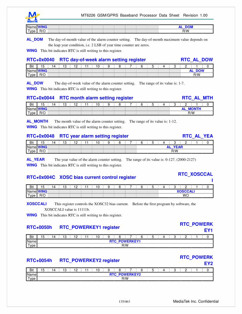
MT6226 GSM/GPRS Baseband Processor Data Sheet Revision 1.00
135/463 MediaTek Inc. Confidential
Name WING AL_DOM Type R/O R/W
AL_DOM The day-of-month value of the alarm counter setting. The day-of-month maximum value depends on
the leap year condition, i.e. 2 LSB of year time counter are zeros. WING This bit indicates RTC is still writing to this register.
RTC+0x0040 RTC day-of-week alarm setting register RTC_AL_DOW Bit 15 14 13 12 11 10 9 8 7 6 5 4 3 2 1 0
Name WING AL_DOW Type R/O R/W
AL_DOW The day-of-week value of the alarm counter setting. The range of its value is: 1-7. WING This bit indicates RTC is still writing to this register.
RTC+0x0044 RTC month alarm setting register RTC_AL_MTH Bit 15 14 13 12 11 10 9 8 7 6 5 4 3 2 1 0
Name WING AL_MONTH Type R/O R/W
AL_MONTH The month value of the alarm counter setting. The range of its value is: 1-12. WING This bit indicates RTC is still writing to this register.
RTC+0x0048 RTC year alarm setting register RTC_AL_YEA Bit 15 14 13 12 11 10 9 8 7 6 5 4 3 2 1 0
Name WING AL_YEAR Type R/O R/W
AL_YEAR The year value of the alarm counter setting. The range of its value is: 0-127. (2000-2127) WING This bit indicates RTC is still writing to this register.
RTC+0x004C XOSC bias current control register RTC_XOSCCAL
I Bit 15 14 13 12 11 10 9 8 7 6 5 4 3 2 1 0
Name WING XOSCCALI Type R/O WO
XOSCCALI This register controls the XOSC32 bias current. Before the first program by software, the
XOSCCALI value is 11111b. WING This bit indicates RTC is still writing to this register.
RTC+0050h RTC_POWERKEY1 register RTC_POWERK
EY1 Bit 15 14 13 12 11 10 9 8 7 6 5 4 3 2 1 0
Name RTC_POWERKEY1 Type R/W
RTC+0054h RTC_POWERKEY2 register RTC_POWERK
EY2 Bit 15 14 13 12 11 10 9 8 7 6 5 4 3 2 1 0
Name RTC_POWERKEY2 Type R/W

MT6226 GSM/GPRS Baseband Processor Data Sheet Revision 1.00
136/463 MediaTek Inc. Confidential
These register sets are used to determine if the real time clock has been programmed by software; i.e. the time value in real time clock is correct. When the real time clock is first powered on, the register contents are all undefined, therefore the time values shown are incorrect. Software needs to know if the real time clock has been programmed. Hence, these two registers are defined to solve this power-on issue. After software programs the correct value, these two register sets do not need to be updated. In addition to programming the correct time value, when the contents of these register sets are wrong, the interrupt is not generated. Therefore, the real time clock does not generate the interrupts before the software programs the registers; unwanted interrupt due to wrong time value do not occur. The correct values of these two register sets are:
RTC_POWERKEY1 A357h RTC_POWERKEY2 67D2h
RTC+0058h PDN1 RTC_PDN1 Bit 15 14 13 12 11 10 9 8 7 6 5 4 3 2 1 0
Name WING DBING RTC_PDN1[7:0]
Type R/O R/O R/W
RTC_PDN1[3:1] is for reset de-bounce mechanism. 0 4ms 1 16ms 2 64ms 3 256ms 4 512ms 5 1024ms 6 2048ms 7 4096ms
RTC_PDN1[7:4] & RTC_PDN1[0] is the spare register for software to keep power on and power off state information. DBING This bit indicates RTC is still de-bouncing. WING This bit indicates RTC is still writing to this register.
RTC+005Ch PDN2 RTC_PDN2 Bit 15 14 13 12 11 10 9 8 7 6 5 4 3 2 1 0
Name WING RTC_PDN2[7:0] Type R/O R/W
RTC_PDN2 The spare register for software to keep power on and power off state information. WING This bit indicates RTC is still writing to this register.
RTC+0060h RTC writing completed flag RTC_WOK Bit 15 14 13 12 11 10 9 8 7 6 5 4 3 2 1 0
Name WING3
WING2
WING1
Type R/O R/O R/O
WING1 This bit indicates RTC is still writing POWERKEY1. WING2 This bit indicates RTC is still writing POWERKEY2. WING3 This bit indicates RTC is still writing BBPU.

MT6226 GSM/GPRS Baseband Processor Data Sheet Revision 1.00
137/463 MediaTek Inc. Confidential
4.10 Auxiliary ADC Unit The auxiliary ADC unit is used to monitor the status of battery and charger, identify the plugged peripheral, and perform temperature measurement. There provides 7 input channels for diversified application in this unit.
There provides 2 modes of operation: immediate mode and timer-triggered mode. The mode of each channel can be individually selected through register AUXADC_CON0. For example, if the flag SYN0 in the register AUXADC_CON0 is set, the channel 0 will be set in timer-triggered mode. Otherwise, it’s in immediate mode.
In immediate mode, the A/D converter will sample the value once only when the flag in the register AUXADC_CON1 has been set. For example, if the flag IMM0 in the register AUXADC_CON1 is set, the A/D converter will sample the data for channel 0. The IMM flags should be cleared and set again to initialize another sampling.
The value sampled for the channel 0 will be stored in register AUXADC_DAT0, the value for the channel 1 will be stored in register AUXADC_DAT1, and vice versa.
If the AUTOSET flag in the register AUXADC_CON3 is set, the auto-sample function is enabled. The A/D converter will sample the data for the channel in which the corresponding data register has been read. For example, in case the SYN1 flag is not set, the AUTOSET flag is set, when the data register AUXADC_DAT0 has been read, the A/D converter will sample the next value for the channel 1 immediately.
If multiple channels are selected at the same time, the task will be performed sequentially on every selected channel. For example, if we set AUXADC_CON1 to be 0x7f, that is, all 7 channels are selected, the state machine in the unit will start sampling from channel 6 to channel 0, and save the values of each input channel in the respective registers. The same process also applies in the timer-triggered mode.
In timer-triggered mode, the A/D converter will sample the value for the channels in which the corresponding SYN flags are set when the TDMA timer counts to the value specified in the register TDMA_AUXEV1, which is placed in the TDMA timer. For example, if we set AUXADC_CON0 to be 0x7f, all 7 channels are selected to be in timer-triggered mode. The state machine will make sampling for all 7 channels sequentially and save the values in registers from AUXADC_DAT0 to AUXADC_DAT6, as it does in immediate mode.
There provides a dedicated timer-triggered scheme for channel 0. The scheme is enabled by setting the SYN7 flag in the register AUXADC_CON2. The timing offset for this event is stored in the register TDMA_AUXEV0 in the TDMA timer. The sampled data triggered by this specific event is stored in the register AUXADC_DAT7. It’s used to separate the results of two individual software routines that perform action on the auxiliary ADC unit.
The AUTOCLRn in the register AUXADC_CON3 is set when it’s intended to sample only once after setting timer-triggered mode. If AUTOCLR1 flag has been set, after the data for the channels in timer-triggered mode has been stored, the SYNn flags in the register AUXADC_CON0 will be cleared. Instead, if AUTOCLR0 flag has been set, after the data for the channel 0 has been stored in the register AUXADC_DAT7, the SYN7 flag in the register AUXADC_CON2 will be cleared.
The usage of the immediate mode and timer-triggered mode are mutual exclusive in terms of individual channel.
The PUWAIT_EN bit in the registers AUXADC_CON3 is used to power up the analog port in advance. That ensures that the power has ramped up to the stable state before A/D converter starts the conversion. The analog part will be automatically powered down after the conversion is completed.

MT6226 GSM/GPRS Baseband Processor Data Sheet Revision 1.00
138/463 MediaTek Inc. Confidential
4.10.1 Register Definitions
AUXADC+0000h
Auxiliary ADC control register 0 AUXADC_CON0
Bit 15 14 13 12 11 10 9 8 7 6 5 4 3 2 1 0 Name SYN6 SYN5 SYN4 SYN3 SYN2 SYN1 SYN0 Type R/W R/W R/W R/W R/W R/W R/W Reset 0 0 0 0 0 0 0
SYNn Those 7 bits define whether the corresponding channel is to be sampled or not in timer-triggered mode. It’s
associated with timing offset register TDMA_AUXEV1. It’s supported to set multiple flags. The flags can be automatically clearly after those channel have been sampled if AUTOCLR1 in the register AUXADC_CON3 is set. 0 The channel is not selected. 1 The channel is selected.
AUXADC+0004h
Auxiliary ADC control register 1 AUXADC_CON1
Bit 15 14 13 12 11 10 9 8 7 6 5 4 3 2 1 0 Name IMM6 IMM5 IMM4 IMM3 IMM2 IMM1 IMM0 Type R/W R/W R/W R/W R/W R/W R/W Reset 0 0 0 0 0 0 0
IMMn Those 7 bits are set individually to sample the data for the corresponding channel. It’s supported to set
multiple flags. 0 The channel is not selected. 1 The channel is selected.
AUXADC+0008h
Auxiliary ADC control register 2 AUXADC_CON2
Bit 15 14 13 12 11 10 9 8 7 6 5 4 3 2 1 0 Name SYN7 Type R/W Reset 0
SYN7 This bit is used only for channel 0 and to be associated with timing offset register TDMA_AUXEV0 in the
TDMA timer in timer-triggered mode. The flag can be automatically clearly after channel 0 have been sampled if AUTOCLR0 in the register AUXADC_CON3 is set. 0 The channel is not selected. 1 The channel is selected.
AUXADC+000Ch
Auxiliary ADC control register 3 AUXADC_CON3
Bit 15 14 13 12 11 10 9 8 7 6 5 4 3 2 1 0
Name AUTOSET
PUWAIT_E
N AUTO
CLR1 AUTOCLR0 STA
Type R/W R/W R/W R/W RO Reset 0 0 0 0 0
AUTOSET The field defines the auto-sample mode of the module. In auto-sample mode, each channel with its sample
register being read can start sampling immediately without configuring the control register AUXADC_CON1 again.

MT6226 GSM/GPRS Baseband Processor Data Sheet Revision 1.00
139/463 MediaTek Inc. Confidential
PUWAIT_EN The field enables the power warm-up period to ensure power stability before the SAR process take place. It’s recommended to activate. 0 The mode is not enabled. 1 The mode is enabled.
AUTOCLR1 The field defines the auto-clear mode of the module for event 1. In auto-clear mode, each timer-triggered channel get the samples of the specified channels once after the SYNn bit in the register AUXADC_CON0 have been set. The SYNn bits will be automatically be cleared and the channel will not being enabled again by the timer event except the SYNn flags are set again. 0 The automatic clear mode is not enabled. 1 The automatic clear mode is enabled.
AUTOCLR0 The field defines the auto-clear mode of the module for event 0. In auto-clear mode, the timer-triggered channel 0 get the sample once after the SYN7 bit in the register AUXADC_CON2 have been set. The SYN7 bit will be automatically cleared and the channel will not be enabled again by the timer event 0 except the SYN7 flag is set again. 0 The automatic clear mode is not enabled. 1 The automatic clear mode is enabled.
STA The field defines the state of the module. 0 This module is idle. 1 This module is busy.
AUXADC+0010h
Auxiliary ADC channel 0 register AUXADC_DAT0
Bit 15 14 13 12 11 10 9 8 7 6 5 4 3 2 1 0 Name DAT Type RO Reset 0
The register stores the sampled data for the channel 0. There are 8 registers of the same type for the corresponding channel. The overall register definition is listed in Table 30.
Register Address Register Function Acronym AUXADC+0010h Auxiliary ADC channel 0 data register AUXADC_DAT0
AUXADC+0014h Auxiliary ADC channel 1 data register AUXADC_DAT1
AUXADC+0018h Auxiliary ADC channel 2 data register AUXADC_DAT2
AUXADC+001Ch Auxiliary ADC channel 3 data register AUXADC_DAT3
AUXADC+0020h Auxiliary ADC channel 4 data register AUXADC_DAT4
AUXADC+0024h Auxiliary ADC channel 5 data register AUXADC_DAT5
AUXADC+0028h Auxiliary ADC channel 6 data register AUXADC_DAT6
AUXADC+002Ch Auxiliary ADC channel 0 data register for TDMA event 0 AUXADC_DAT7
Table 30 Auxiliary ADC data register list
4.11 I2C / SCCB
4.11.1 General Description I2C (Inter-IC) /SCCB (Serial Camera Control Bus) is a two-wire serial master interface. The two signals are SIO_CK and SIO_DAT. SIO_CK is a single-direction, active-high clock signal that must be driven by the master. SIO_DAT is a bi-directional data signal that can be driven by either the master or the slave.

MT6226 GSM/GPRS Baseband Processor Data Sheet Revision 1.00
140/463 MediaTek Inc. Confidential
Within the transmission, two situations are defined as the START and STOP conditions. A HIGH to LOW transition on the SIO_DAT line while SIO_CK is high indicates a START condition. A LOW to HIGH transition on the SIO_DAT line while SIO_CK is high indicates a STOP condition. The master generates START and STOP conditions when it initiates or terminates a transmission.
This I2C/SCCB master supports the following types of transfer formats: 2 phase write, 2 phase read, 3 phase write, 3phase read, and 4 phase write. Each transmission is encapsulated with a start and stop condition. Repeated start condition is not supported. Each phase within a transfer consists of 9 bit serial transmission, where the first 8 bits contains the data and the 9th bit is for acknowledgement condition. The transfer formats are depicted in Figure 79 I2C/SCCB transfer formats below.
Figure 79 I2C/SCCB transfer formats
Most external I2C/SCCB devices can be supported using a combination of these types of transfer format. Different transfer format is selected through configuring the data length register and indicating the read/write transfer direction.
For example, for an 8 bit write to a camera sensor, it can use the 3 phase write transfer as shown in Figure 80 8 bit write example
ID Address Sub-address Write Data
Figure 80 8 bit write example
And for an 8 bit read, it can use the 2 phase write transfer followed by a 2 phase read transfer as shown in Figure 81 8 bit read example.
ID Address Sub-address
Phase 1 Phase 2
ID Address Read Data
Phase 1 Phase 2
Figure 81 8 bit read example

MT6226 GSM/GPRS Baseband Processor Data Sheet Revision 1.00
141/463 MediaTek Inc. Confidential
For a 16 bit write to a camera sensor, the 4 phase write transfer can be used. And for the 16 bit read, the 2 phase write transfer followed by a 3 phase read transfer can be used.
4.11.2 Register Definitions
SCCB+0000h SCCB Control Register CTRL Bit 15 14 13 12 11 10 9 8 7 6 5 4 3 2 1 0
Name SCCB_EN
Type R/W Reset 0
SCCB_EN This bit is used to enable SCCB. The bit must be accessed when SCCB wants to communicate with the
slave, i.e. generates write or read transmission cycles.
SCCB+0008h SCCB Data Length Register DAT_LEN Bit 15 14 13 12 11 10 9 8 7 6 5 4 3 2 1 0
Name DAT_LEN Type R/W Reset 0
DAT_LEN This field indicates the transmission length minus 1. For 2 Phase transmission, set DAT_LEN = 1. For 3-phase transmission, set DAT_LEN = 2. For 4-phase transmission, set DAT_LEN = 3.
SCCB+000Ch SCCB Buffer Time Register TBUF Bit 15 14 13 12 11 10 9 8 7 6 5 4 3 2 1 0
Name TBUF Type R/W Reset 3Eh
TBUF For SCCB, the master initiates transmission with a START condition, and ends the transmission by sending a
STOP condition. TBUF indicates the bus free time between a STOP and START condition, i.e. the interval of the STOP and START conditions. Based on a 13 MHz clock frequency, the SCCB buffer time = (TBUF / 13000000), and the default setting is ~4.7us.
SCCB+0010h SCCB Start Hold Time THDSTA Bit 15 14 13 12 11 10 9 8 7 6 5 4 3 2 1 0
Name THDSTA Type R/W Reset 34h
THDSTA START condition occurs when there is a HIGH to LOW transition on the SIO_DAT line while SIO_CK is
HIGH. The START hold time indicates that SIO_CK should be HIGH at least THDSTA length of time after SIO_DAT becomes LOW. Based on a 13 MHz frequency, the SCCB start hold time = (THDSTA / 13000000), and the default setting is ~4us.
SCCB+0014h SCCB Data Hold Time THDDAT Bit 15 14 13 12 11 10 9 8 7 6 5 4 3 2 1 0
Name THDDAT Type R/W Reset 27h

MT6226 GSM/GPRS Baseband Processor Data Sheet Revision 1.00
142/463 MediaTek Inc. Confidential
THDDAT Since SCCB data can be changed only when SIO_CK is LOW, a data hold time is defined to indicate the time interval that data cannot be changed after SIO_CK becomes LOW. Based on 13 MHz frequency, SCCB data hold time = (THDDAT / 13000000), and the default setting is ~3us.
SCCB+0018h SCCB TLOW TLOW Bit 15 14 13 12 11 10 9 8 7 6 5 4 3 2 1 0
Name TLOW Type R/W Reset 46h
TLOW This field indicates the low period of serial clock. Combined with THIGH, the SIO_CK duty is adjustable.
Based on a 13MHz frequency, the SIO_CK low period = (TLOW / 13000000), and the default setting is ~5.3us.
SCCB+001Ch SCCB THIGH THIGH Bit 15 14 13 12 11 10 9 8 7 6 5 4 3 2 1 0
Name THIGH Type R/W Reset 3Ch
THIGH This field indicates the high period of serial clock. Combined with TLOW, the SIO_CK duty is adjustable.
Based on a 13 MHz frequency, the SIO_CK high period = (THIGH / 13000000), and the default setting is ~4.6us.
SCCB+0020h SCCB Data Register DATA Bit 15 14 13 12 11 10 9 8 7 6 5 4 3 2 1 0
Name DATA Type R/W Reset 0
DATA SCCB write data. This is the input to the internal transmit fifo and contains the value and control
information of the data that is to be transmitted on the bus. Data[7:0] contains the actual value to be transmitted. For a N-phase WRITE transfer, all N bytes must be inputted to the fifo. For a N-phase READ transfer, only the first byte needs to be inputted to the fifo.
DATA[8] DATA[8] must be set to 1 for the first phase of the transfer, which also represents the ID address to be transmitted. For all other phases of the transfer, this bit must be 0. When this bit is set to 1, data[0] is checked to determine the transfer direction.
DATA[0] If DATA [8] = 1, then:
DATA [0] = 0 indicates that the rest of the transfer is a write transfer DATA [0] = 1 indicates that the rest of the transfer is a read transfer
SCCB+0028h SCCB STOP Setup Time TSUSTO Bit 15 14 13 12 11 10 9 8 7 6 5 4 3 2 1 0
Name TSUSTO Type R/W Reset 34h
TSUSTO A LOW to HIGH transition on the SIO_DAT line while SIO_CK is high indicates a STOP condition.
For a STOP condition, the LOW to HIGH transition on the SIO_DAT can be generated after SCCB STOP setup time while SIO_CK must be HIGH. Based on a 13 MHz frequency, SCCB STOP setup time = (TSUSTOP / 13000000), and the default setting is ~4us.

MT6226 GSM/GPRS Baseband Processor Data Sheet Revision 1.00
143/463 MediaTek Inc. Confidential
SCCB+0038h SCCB MODE MODE Bit 15 14 13 12 11 10 9 8 7 6 5 4 3 2 1 0
Name MODE
Type R/W Reset 0
MODE This bit indicates the SCCB operating mode
0 To operate as Slave 1 To operate as Master
SCCB+003Ch SCCB Buf Clear BUF_CLEAR Bit 15 14 13 12 11 10 9 8 7 6 5 4 3 2 1 0
Name BUF_CLEA
R Type R/W Reset 0
BUF_CLEAR Buffer clear bit. Set this bit to clear the SCCB FIFO.
0 Buffer is not cleared. 1 Clear the buffer.
SCCB+0040h SCCB Status Register STA Bit 15 14 13 12 11 10 9 8 7 6 5 4 3 2 1 0
Name WRITE READ
Type R/W R/W Reset 0 0
READ Indicates the read is complete.
0 Read command is not finished. 1 Read command is finished.
WRITE Indicates the write is complete. 0 Write command is not finished. 0 Write command is finished.
SCCB+0044h SCCB Read Data Register High Byte READ_DATA Bit 15 14 13 12 11 10 9 8 7 6 5 4 3 2 1 0
Name READ_DATA Type RO Reset 8’hBE
READ_DATA The returned read data from slave. For 8 bit read, this returns the data received. For 16 bit read, this
returns the first byte returned (which is the High Byte).
SCCB+0048h SCCB Read Data Register Low Byte READ_DATA_L Bit 15 14 13 12 11 10 9 8 7 6 5 4 3 2 1 0
Name READ_DATA_L Type RO Reset 8’hEF
READ_DATA_L The returned read data from slave. For 8 bit read, the value in this register in invalid. For 16 bit read,
this returns the second byte returned (which is the Low Byte).

MT6226 GSM/GPRS Baseband Processor Data Sheet Revision 1.00
144/463 MediaTek Inc. Confidential
SCCB+0070h SCCB Read Data Clear READ_DATA_C
LR Bit 15 14 13 12 11 10 9 8 7 6 5 4 3 2 1 0
Name READ_DATA_CLR
Type WO Reset
READ_DATA_CLr Writing a 1 to this register generates a synchronous reset pulse to clear the value of
READ_DATA and READ_DATA_L.

MT6226 GSM/GPRS Baseband Processor Data Sheet Revision 1.00
145/463 MediaTek Inc. Confidential
5 Microcontroller Coprocessors
Microcontroller Coprocessors are designed to run computing-intensive processes in place of the Microcontroller (MCU). These coprocessors especially target timing critical GSM/GPRS Modem processes that require fast response and large data movement. Controls to the coprocessors are all through memory access via the APB.
5.1 Divider To ease the processing load of the MCU, a divider is employed. The divider can perform signed and unsigned 32bit/32bit division, as well as modulus. The processing time of the divider is from 1 clock cycle to 33 clock cycles, depending on the magnitude of the dividend. Detailed processing times are listed below in Table 31. Table 31 shows two processing times (except for when the dividend is zero) for each range of dividends, depending on whether or not restoration is required during the last step of the division operation.
Table 31: Processing Time for Different Dividend Values
Signed Division Unsigned Division
Dividend Clock Cycles Dividend Clock Cycles
0000_0000h 1 0000_0000h 1
0000_00ffh – (-0000_0100h), excluding 0x0000_0000
8 or 9 0000_0001h - 0000_00ffh 8 or 9
0000_ffffh – (-0001_0000h) 16 or 17 0000_0100h - 0000_ffffh 16 or 17
00ff_ffffh – (-0100_0000h) 24 or 25 0001_0000h - 00ff_ffffh 24 or 25
7fff_ffffh – (-8000_0000h) 32 or 33 0100_0000h - ffff_ffffh 32 or 33
When the divider is started by setting the Divider Control Register START bit to 1, DIV_RDY becomes 0; this bit is asserted when the division process is complete. MCU detects this status bit by polling it to know the correct access timing. To simplify polling, only the value of register DIV_RDY is visible while Divider Control Register is being read. Hence, MCU does not need to mask other bits to extract the value of DIV_RDY.
In a GSM/GPRS system, many divisions are executed with constant divisors. Therefore, oft-used constants are stored in the divider to speed up the process. By controlling control bits IS_CNST and CNST_IDX in Divider Control register, a division can be performed without providing a divisor. This omission of a step saves on the time for writing a divisor in and on the instruction fetch time, thus making the process more efficient.
5.1.1 Register Definitions
DIVIDER+0000h
Divider Control Register DIV_CON
Bit 31 30 29 28 27 26 25 24 23 22 21 20 19 18 17 16 Name CNST_IDX Type WO Reset 0
Bit 15 14 13 12 11 10 9 8 7 6 5 4 3 2 1 0
Name IN_CNST SIGN DIV_RD
Y STAR
T Type WO WO RO WO Reset 0 1 1 0

MT6226 GSM/GPRS Baseband Processor Data Sheet Revision 1.00
146/463 MediaTek Inc. Confidential
START Starts a division operation. Returns to 0 after the division has started. DIV_RDY Current status of the divider. Note that when DIV_CON register is read, only the value of DIV_RDY
appears; the program does not need to mask other parts of the register to extract the information in DIV_RDY. 0 Division is in progress. 1 Division is finished
SIGN Indicates a signed or unsigned division operation. 0 Unsigned division 1 Signed division
IS_CNST Specifies that an internal constant value should be used as a divisor. If IS_CNST is enabled, the divisor value need not be written, and divider automatically uses the internal constant value instead. The internal constant value used depends on the value of CNST_IDX. 0 Normal division. Divisor is written in via APB. 1 Using internal constant divisor instead.
CNST_IDX Index of constant divisor. 0 divisor = 13 1 divisor = 26 2 divisor = 51 3 divisor = 52 4 divisor = 102 5 divisor = 104
DIVIDER +0004h
Divider Dividend register DIV_DIVIDEND
Bit 31 30 29 28 27 26 25 24 23 22 21 20 19 18 17 16 Name DIVIDEND[31:16] Type WO Reset 0
Bit 15 14 13 12 11 10 9 8 7 6 5 4 3 2 1 0 Name DIVIDEND[15:0] Type WO Reset 0
Dividend.
DIVIDER +0008h
Divider Divisor register DIV_DIVISOR
Bit 31 30 29 28 27 26 25 24 23 22 21 20 19 18 17 16 Name DIVISOR[31:16] Type WO Reset 0
Bit 15 14 13 12 11 10 9 8 7 6 5 4 3 2 1 0 Name DIVISOR[15:0] Type WO Reset 0
Divisor.
DIVIDER +000Ch
Divider Quotient register DIV_QUOTIENT
Bit 31 30 29 28 27 26 25 24 23 22 21 20 19 18 17 16

MT6226 GSM/GPRS Baseband Processor Data Sheet Revision 1.00
147/463 MediaTek Inc. Confidential
Name QUOTIENT[31:16] Type RO Reset 0
Bit 15 14 13 12 11 10 9 8 7 6 5 4 3 2 1 0 Name QUOTIENT[15:0] Type RO Reset 0
Quotient.
DIVIDER +0010h
Divider Remainder register DIV_REMAINDE
R Bit 31 30 29 28 27 26 25 24 23 22 21 20 19 18 17 16
Name REMAINDER[31:16] Type RO Reset 0
Bit 15 14 13 12 11 10 9 8 7 6 5 4 3 2 1 0 Name REMAINDER[15:0] Type RO Reset 0
Remainder.
5.2 CSD Accelerator
5.2.1 General Description This unit performs the data format conversion of RA0, RA1, and FAX in CSD service. CSD service consists of two major functions: data flow throttling and data format conversion. The data format conversion is a bit-wise operation and requires several instructions to complete a conversion, thus making it inefficient for the MCU to perform itself. A coprocessor, CSD accelerator, is designed to reduce the computing power needed to perform this function.
The CSD accelerator helps in converting data format only; the data flow throttling function is still implemented by the MCU. CSD accelerator performs three types of data format conversion: RA0, RA1, and FAX.
For RA0 conversion, too many case scenarios for the downlink path conversion greatly increase the hardware area cost, thus only uplink RA0 data format conversion is provided. Uplink RA0 conversion consists of inserting a start bit before and a stop bit after each a byte, for a duration of 16 bytes. Figure 87 illustrates the detailed conversion table.
Figure 87: Data Format Conversion of RA0

MT6226 GSM/GPRS Baseband Processor Data Sheet Revision 1.00
148/463 MediaTek Inc. Confidential
The RA0 converter processes data state by state. Therefore, before filling in new data, software must ensure that converted data of in a state is withdrawn, otherwise the converted data is replaced by new data. For example, if 32 bits of data are written, the state pointer increments from state 0 to state 1, and word ready of state 0 is asserted. Before writing the next 32-bit data, the word of state 0 must be withdrawn first, or the data is lost when the next conversion is performed.
RA0 records the number of written bytes, the state pointer, and a ready state word. This information helps the software to perform flow control. See Register Definition for more detail.
For RA1 conversion, both downlink and uplink directions are supported. The data formats vary for different data rate. Detailed conversion tables are shown in Figure 88 and Figure 89. The yellow part is the payload data, and the blue part is the status bit.
Figure 88: Data Format Conversion for 6k/12k RA1

MT6226 GSM/GPRS Baseband Processor Data Sheet Revision 1.00
149/463 MediaTek Inc. Confidential
Figure 89: Data Format Conversion for 3.6k RA1
For FAX, two types of bit-reversal functions are provided. Type 1 reversal is a bit-wise reversal (Figure 90), and Type 2 is a byte-wise reversal (Figure 91).
Figure 90: Type 1 Bit Reversal
Figure 91: Type 2 Bit Reversal
Table 34: CSD Accelerator Registers
Register Address Register Function Acronym
CSD + 0000h CSD RA0 Control Register CSD_RA0_CON CSD + 0004h CSD RA0 Status Register CSD_RA0_STA CSD + 0008h CSD RA0 Input Data Register CSD_RA0_DI CSD + 000Ch CSD RA0 Output Data Register CSD_RA0_DO CSD + 0100h CSD RA1 6K/12K Uplink Input Data Register 0 CSD_RA1_6_12K_ULDI0 CSD + 0104h CSD RA1 6K/12K Uplink Input Data Register 1 CSD_RA1_6_12K_ULDI1 CSD + 0108h CSD RA1 6K/12K Uplink Status Data Register CSD_RA1_6_12K_ULSTUS CSD + 010Ch CSD RA1 6K/12K Uplink Output Data Register 0 CSD_RA1_6_12K_ULDO0

MT6226 GSM/GPRS Baseband Processor Data Sheet Revision 1.00
150/463 MediaTek Inc. Confidential
CSD + 0110h CSD RA1 6K/12K Uplink Output Data Register 1 CSD_RA1_6_12K_ULDO1 CSD + 0200h CSD RA1 6K/12K Downlink Input Data Register 0 CSD_RA1_6_12K_DLDI0 CSD + 0204h CSD RA1 6K/12K Downlink Input Data Register 1 CSD_RA1_6_12K_DLDI1 CSD + 0208h CSD RA1 6K/12K Downlink Output Data Register 0 CSD_RA1_6_12K_DLDO0 CSD + 020Ch CSD RA1 6K/12K Downlink Output Data Register 1 CSD_RA1_6_12K_DLDO1 CSD + 0210h CSD RA1 6K/12K Downlink Status Data Register CSD_RA1_6_12K_DLSTUS CSD + 0300h CSD RA13.6K Uplink Input Data Register 0 CSD_RA1_3P6K_ULDI0 CSD + 0304h CSD RA13.6K Uplink Status Data Register CSD_RA1_3P6K_ULSTUS CSD + 0308h CSD RA13.6K Uplink Output Data Register 0 CSD_RA1_3P6K_ULDO0 CSD + 030Ch CSD RA13.6K Uplink Output Data Register 1 CSD_RA1_3P6K_ULDO1 CSD + 0400h CSD RA1 3.6K Downlink Input Data Register 0 CSD_RA1_3P6K_DLDI0 CSD + 0404h CSD RA1 3.6K Downlink Input Data Register 1 CSD_RA1_3P6K_DLDI1 CSD + 0408h CSD RA1 3.6K Downlink Output Data Register 0 CSD_RA1_3P6K_DLDO0 CSD + 040Ch CSD RA1 3.6K Downlink Status Data Register CSD_RA1_3P6K_DLSTUS CSD + 0500h CSD FAX Bit Reverse Type 1 Input Data Register CSD_FAX_BR1_DI CSD + 0504h CSD FAX Bit Reverse Type 1 Output Data Register CSD_FAX_BR1_DO CSD + 0510h CSD FAX Bit Reverse Type 2 Input Data Register CSD_FAX_BR2_DI CSD + 0514h CSD FAX Bit Reverse Type 2 Output Data Register CSD_FAX_BR2_DO
5.2.2 Register Definitions
CSD+0000h CSD RA0 Control Register CSD_RA0_CON Bit 31 30 29 28 27 26 25 24 23 22 21 20 19 18 17 16
Name Type Reset
Bit 15 14 13 12 11 10 9 8 7 6 5 4 3 2 1 0 Name RST BTS0 VLD_BYTE Type WO WO WO Reset 0 0 100
VLD_BYTE Specifies the number of valid bytes in the current input data. This value must be specified before filling
data. BTS0 Back to state 0. Forces RA0 converter return back to state 0. Incomplete words are padded with stop bits.
For example, consider a back-to-state0 command that is issued after 8 bytes of data are filled in. All bits after the 8th byte are padded with stop bits, and the second ready word byte RDYWD2 is asserted. After removing state word 2, the state pointer goes back to state 0. Note that new data filling should take place after removing state word 2, or the state pointer may be out of order.
Figure 92: Example of Back to State 0

MT6226 GSM/GPRS Baseband Processor Data Sheet Revision 1.00
151/463 MediaTek Inc. Confidential
RST Resets the RA0 converter. If an erroneous operation disorders the data, this bit restores all states to their
original state.
CSD+0004h CSD RA0 Status Register CSD_RA0_STA Bit 31 30 29 28 27 26 25 24 23 22 21 20 19 18 17 16
Name Type Reset
Bit 15 14 13 12 11 10 9 8 7 6 5 4 3 2 1 0 Name BYTECNT CRTSTA RDYWD Type RO RO RC Reset 0 0 0
RDYWD0~4 Ready words. Indicates which state words are ready for withdrawal. If any bits asserted, data
must be withdrawn before new data is filled into CSD_RA0_DI, to avoid data loss. 0 Not ready 1 Ready
CRTSTA Current state. State0 ~ State4. Indicates which state word software is currently filling. BYTECNT Total number of bytes being filled.
CSD+0008h CSD RA0 Input Data Register CSD_RA0_DI Bit 31 30 29 28 27 26 25 24 23 22 21 20 19 18 17 16
Name DIN Type WO Reset 0
Bit 15 14 13 12 11 10 9 8 7 6 5 4 3 2 1 0 Name DIN Type WO Reset 0
DIN The RA0 conversion input data. The ready word indicator is checked before filling in data; if any words are
ready, they are withdrawn first, otherwise the ready data in RA0 converter is replaced.
CSD+000Ch CSD RA0 Output Data Register CSD_RA0_DO Bit 31 30 29 28 27 26 25 24 23 22 21 20 19 18 17 16
Name DOUT Type RO Reset 0
Bit 15 14 13 12 11 10 9 8 7 6 5 4 3 2 1 0 Name DOUT Type RO Reset 0

MT6226 GSM/GPRS Baseband Processor Data Sheet Revision 1.00
152/463 MediaTek Inc. Confidential
DOUT RA0 converted data. The return data corresponds to the ready word indicator defined in CSD_RA0_STA register. The five bits of RDYWD map to state0 ~ state 4 respectively. When CSD_RA0_DO is read, the asserted state word is returned. If two state words asserted at the same time, the lower one is returned.
CSD+0100h CSD RA1 6K/12K Uplink Input Data Register 0 CSD_RA1_6_12
K_ULDI0 Bit 31 30 29 28 27 26 25 24 23 22 21 20 19 18 17 16
Name DIN Type WO Reset 0
Bit 15 14 13 12 11 10 9 8 7 6 5 4 3 2 1 0 Name DIN Type WO Reset 0
DIN D1 to D32 of the RA1 uplink data.
CSD+0104h CSD RA1 6K/12K Uplink Input Data Register 1 CSD_RA1_6_12
K_ULDI1 Bit 31 30 29 28 27 26 25 24 23 22 21 20 19 18 17 16
Name Type Reset
Bit 15 14 13 12 11 10 9 8 7 6 5 4 3 2 1 0 Name DIN Type WO Reset 0
DIN D33 to D48 of the RA1 uplink data.
CSD+0108h CSD RA1 6K/12K Uplink Status Data Register CSD_RA1_6_12
K_ULSTUS Bit 31 30 29 28 27 26 25 24 23 22 21 20 19 18 17 16
Name Type Reset
Bit 15 14 13 12 11 10 9 8 7 6 5 4 3 2 1 0 Name E7 E6 E5 E4 X SB SA Type WO WO WO WO WO WO WO Reset 0 0 0 0 0 0 0
SA Represents S1, S3, S6, and S8 of the status bits. SB Represents S4 and S9 of the status bits. X Represents X of the status bits. E4 Represents E4 of the status bits. E5 Represents E5 of the status bits. E6 Represents E6 of the status bits. E7 Represents E7 of the status bits.
CSD+010Ch CSD RA1 6K/12K Uplink Output Data Register 0 CSD_RA1_6_12
K_ULDO0 Bit 31 30 29 28 27 26 25 24 23 22 21 20 19 18 17 16
Name DOUT Type RO Reset 0

MT6226 GSM/GPRS Baseband Processor Data Sheet Revision 1.00
153/463 MediaTek Inc. Confidential
Bit 15 14 13 12 11 10 9 8 7 6 5 4 3 2 1 0 Name DOU Type RO Reset 0
DOUT Bit 0 to bit 31 of the RA1 6K/12K uplink frame.
CSD+0110h CSD RA1 6K/12K Uplink Output Data Register 1 CSD_RA1_6_12
K_ULDO1 Bit 31 30 29 28 27 26 25 24 23 22 21 20 19 18 17 16
Name DOUT Type RO Reset 0
Bit 15 14 13 12 11 10 9 8 7 6 5 4 3 2 1 0 Name DOUT Type RO Reset 0
DOUT Bit 32 to bit 59 of the RA1 6K/12K uplink frame.
CSD+0200h CSD RA1 6K/12K Downlink Input Data Register 0 CSD_RA1_6_12
K_DLDI0 Bit 31 30 29 28 27 26 25 24 23 22 21 20 19 18 17 16
Name DIN Type WO Reset 0
Bit 15 14 13 12 11 10 9 8 7 6 5 4 3 2 1 0 Name DIN Type WO Reset 0
DIN Bit 0 to bit 31 of the RA1 6K/12K downlink frame.
CSD+0204h CSD RA1 6K/12K Downlink Input Data Register 1 CSD_RA1_6_12
K_DLDI1 Bit 31 30 29 28 27 26 25 24 23 22 21 20 19 18 17 16
Name DIN Type WO Reset 0
Bit 15 14 13 12 11 10 9 8 7 6 5 4 3 2 1 0 Name DIN Type WO Reset 0
DIN Bit 32 to bit 59 of the RA1 6K/12K downlink frame.
CSD+0208h CSD RA1 6K/12K Downlink Output Data Register 0 CSD_RA1_6_12
K_DLDO0 Bit 31 30 29 28 27 26 25 24 23 22 21 20 19 18 17 16
Name DOUT Type RO Reset 0
Bit 15 14 13 12 11 10 9 8 7 6 5 4 3 2 1 0 Name DOUT Type RO Reset 0
DOUT D1 to D32 of the RA1 downlink data.

MT6226 GSM/GPRS Baseband Processor Data Sheet Revision 1.00
154/463 MediaTek Inc. Confidential
CSD+020Ch CSD RA1 6K/12K Downlink Output Data Register 1 CSD_RA1_6_12
K_DLDO1 Bit 31 30 29 28 27 26 25 24 23 22 21 20 19 18 17 16
Name Type Reset
Bit 15 14 13 12 11 10 9 8 7 6 5 4 3 2 1 0 Name DOUT Type RO Reset 0
DOUT D33 to D48 of the RA1 downlink data.
CSD+0210h CSD RA1 6K/12K Downlink Status Data Register CSD_RA1_6_12
K_DLSTUS Bit 31 30 29 28 27 26 25 24 23 22 21 20 19 18 17 16
Name Type Reset
Bit 15 14 13 12 11 10 9 8 7 6 5 4 3 2 1 0 Name E7 E6 E5 E4 X SB SA Type RO RO RO RO RO RO RO Reset 0 0 0 0 0 0 0
SA The majority vote of the S1, S3, S6 and S8 status bits. If the vote is split, SA=0. SB The majority vote of the S4 and S9 status bits. If the vote is split, SB=0. X The majority vote of the two X bits in downlink frame. If the vote is split, X=0. E4 Represents E4 of the status bits. E5 Represents E5 of the status bits. E6 Represents E6 of the status bits. E7 Represents E7 of the status bits.
CSD+0300h CSD RA1 3.6K Uplink Input Data Register 0 CSD_RA1_3P6
K_ULDI0 Bit 31 30 29 28 27 26 25 24 23 22 21 20 19 18 17 16
Name DIN Type WO Reset 0
Bit 15 14 13 12 11 10 9 8 7 6 5 4 3 2 1 0 Name DIN Type WO Reset 0
DIN D1 to D24 of the RA1 3.6K uplink data.
CSD+0304h CSD RA1 3.6K Uplink Status Data Register CSD_RA1_3P6
K_ULSTUS Bit 31 30 29 28 27 26 25 24 23 22 21 20 19 18 17 16
Name Type Reset
Bit 15 14 13 12 11 10 9 8 7 6 5 4 3 2 1 0 Name E7 E6 E5 E4 X SB SA Type WO WO WO WO WO WO WO Reset 0 0 0 0 0 0 0

MT6226 GSM/GPRS Baseband Processor Data Sheet Revision 1.00
155/463 MediaTek Inc. Confidential
SA Represents S1, S3, S6, and S8 of the status bits. SB Represents S4 and S9 of the status bits. X Represents X of the status bits. E4 Represents E4 of the status bits. E5 Represents E5 of the status bits. E6 Represents E6 of the status bits. E7 Represents E7 of the status bits.
CSD+0308h CSD RA1 3.6K Uplink Output Data Register 0 CSD_RA1_3P6
K_ULDO0 Bit 31 30 29 28 27 26 25 24 23 22 21 20 19 18 17 16
Name DOUT Type RO Reset 0
Bit 15 14 13 12 11 10 9 8 7 6 5 4 3 2 1 0 Name DOUT Type RO Reset 0
DOUT Bit 0 to bit 31 of the RA1 3.6K uplink frame.
CSD+030Ch CSD RA1 3.6K Uplink Output Data Register 1 CSD_RA1_3P6
K_ULDO1 Bit 31 30 29 28 27 26 25 24 23 22 21 20 19 18 17 16
Name Type Reset
Bit 15 14 13 12 11 10 9 8 7 6 5 4 3 2 1 0 Name DOUT Type RO Reset 0
DOUT Bit 32 to bit 35 of the RA1 3.6K uplink frame.
CSD+0400h CSD RA1 3.6K Downlink Input Data Register 0 CSD_RA1_3P6
K_DLDI0 Bit 31 30 29 28 27 26 25 24 23 22 21 20 19 18 17 16
Name DIN Type WO Reset 0
Bit 15 14 13 12 11 10 9 8 7 6 5 4 3 2 1 0 Name DIN Type WO Reset 0
DIN Bit 0 to bit 31 of the RA1 3.6K downlink frame.
CSD+0404h CSD RA1 3.6K Downlink Input Data Register 1 CSD_RA1_3P6
K_DLDI1 Bit 31 30 29 28 27 26 25 24 23 22 21 20 19 18 17 16
Name Type Reset
Bit 15 14 13 12 11 10 9 8 7 6 5 4 3 2 1 0 Name DIN

MT6226 GSM/GPRS Baseband Processor Data Sheet Revision 1.00
156/463 MediaTek Inc. Confidential
Type WO Reset 0
DIN Bit 32 to bit 35 of the RA1 3.6K downlink frame.
CSD+0408h CSD RA1 3.6K Downlink Output Data Register 0 CSD_RA1_3P6
K_DLDO0 Bit 31 30 29 28 27 26 25 24 23 22 21 20 19 18 17 16
Name DOUT Type RO Reset 0
Bit 15 14 13 12 11 10 9 8 7 6 5 4 3 2 1 0 Name DOUT Type RP Reset 0
DIN D1 to D24 of the RA1 3.6K downlink data.
CSD+040Ch CSD RA1 3.6K Downlink Status Data Register CSD_RA1_3P6
K_DLSTUS Bit 31 30 29 28 27 26 25 24 23 22 21 20 19 18 17 16
Name Type Reset
Bit 15 14 13 12 11 10 9 8 7 6 5 4 3 2 1 0 Name E7 E6 E5 E4 X SB SA Type RO RO RO RO RO RO RO Reset 0 0 0 0 0 0 0
SA The majority vote of the S1, S3, S6 and S8 status bits. If the vote is split, SA=0. SB The majority vote of the S4 and S9 status bits. If the vote is split, SB=0. X The majority vote of the two X bits in downlink frame. If the vote is split, X=0. E4 Represents E4 of status bits. E5 Represents E5 of status bits. E6 Represents E6 of status bits. E7 Represents E7 of status bits.
CSD+0500h CSD FAX Bit Reverse Type 1 Input Data Register CSD_FAX_BR1
_DI Bit 31 30 29 28 27 26 25 24 23 22 21 20 19 18 17 16
Name DIN Type WO Reset 0
Bit 15 14 13 12 11 10 9 8 7 6 5 4 3 2 1 0 Name DIN Type WO Reset 0
DIN 32-bit input data for a Type 1 bit reversal of the FAX data. A Type 1 bit reversal reverses the data bit by bit.
CSD+0504h CSD FAX Bit Reverse Type 1 Output Data Register CSD_FAX_BR1
_DO Bit 31 30 29 28 27 26 25 24 23 22 21 20 19 18 17 16
Name DOUT Type RO Reset 0

MT6226 GSM/GPRS Baseband Processor Data Sheet Revision 1.00
157/463 MediaTek Inc. Confidential
Bit 15 14 13 12 11 10 9 8 7 6 5 4 3 2 1 0 Name DOUT Type RO Reset 0
DOUT 32-bit result data for a Type 1 bit reversal of the FAX data.
CSD+0510h CSD FAX Bit Reverse Type 2 Input Data Register CSD_FAX_BR2
_DI Bit 31 30 29 28 27 26 25 24 23 22 21 20 19 18 17 16
Name DIN Type WO Reset 0
Bit 15 14 13 12 11 10 9 8 7 6 5 4 3 2 1 0 Name DIN Type WO Reset 0
DIN 32-bit input data for a Type 2 bit reversal of the FAX data. A Type 2 bit reversal reverses the data byte by
byte.
CSD+0514h CSD FAX Bit Reverse Type 2 Output Data Register CSD_FAX_BR2
_DO Bit 31 30 29 28 27 26 25 24 23 22 21 20 19 18 17 16
Name DOUT Type RO Reset 0
Bit 15 14 13 12 11 10 9 8 7 6 5 4 3 2 1 0 Name DOUT Type RO Reset 0
DOUT 32-bit result data for a Type 2 bit reversal of the FAX data.
5.3 FCS Codec
5.3.1 General Description The Frame Check Sequence (FCS) serves to detect errors in the following information bits:
RLP-frame of CSD services in GSM: The frame length is fixed at 240 or 576 bits including the 24-bit FCS field.
LLC-frame of GPRS service: The frame length is determined by the information field, and length of the FCS field is 24 bits.
Generation of the FCS is very similar to CRC coding in baseband signal processing. ETSI GSM specifications 04.22 and 04.64 both define the coding rules as:
1. The CRC is the one’s complement of the modulo-2 sum of the following additives:
• the remainder of xk(x23 + x22 + x21 + … + x2 + x + 1) modulo-2 divided by the generator polynomial, where k
is the number of bits of the dividend (i.e. fill the shift registers with all ones initially before feeding data); and,

MT6226 GSM/GPRS Baseband Processor Data Sheet Revision 1.00
158/463 MediaTek Inc. Confidential
• the remainder of the modulo-2 division by the generator polynomial of the product of x24 by the dividend, which are the information bits.
2. The CRC-24 generator polynomial is: G(x) = x24 + x23 + x21 + x20 + x19 + x17 + x16 + x15 + x13 + x8 + x7 + x5 + x4 + x2 + 1
3. The 24-bit CRC is appended to the data bits in the MSB-first manner.
4. Decoding is identical to encoding except that data fed into the syndrome circuit is 24 bits longer than the information bits at encoding. The dividend is also multiplied by x24. If no error occurs, the remainder satisfies: R(x) = x22 + x21 + x19 + x18 + x16 + x15 + x11 + x8 + x5 + x4 (0x6d8930) And the parity output word is 0x9276cf.
In contrast to conventional CRC, this special coding scheme makes the encoder identical to the decoder and simplifies the hardware design.
5.3.2 Register Definitions
FCS+0000h FCS input data register FCS_DATA Bit 15 14 13 12 11 10 9 8 7 6 5 4 3 2 1 0
Name D15 D14 D13 D12 D11 D10 D9 D8 D7 D6 D5 D4 D3 D2 D1 D0 Type WO WO WO WO WO WO WO WO WO WO WO WO WO WO WO WO
The data bits input. First write of this register is the starting point of the encode or decode process. D0~15 The input format is D15·xn+ D14·xn-1+ D13·xn-2+ … + Dk·xk+ …, thus D15 is the first bit pushed into the
shift register. If the last data word is less than 16 bits, the remaining bits are neglected.
FCS+0004h Input data length indication register FCS_DLEN Bit 15 14 13 12 11 10 9 8 7 6 5 4 3 2 1 0
Name LEN Type WO
The MCU specifies the total data length (in bits) to be encoded or decoded. LEN Data length. The length must be a multiple of 8 bits.
FCS+0x0008h FCS parity output register 1, MSB part FCS_PAR1 Bit 15 14 13 12 11 10 9 8 7 6 5 4 3 2 1 0
Name P15 P14 P13 P12 P11 P10 P9 P8 P7 P6 P5 P4 P3 P2 P1 P0 Type RC RC RC RC RC RC RC RC RC RC RC RC RC RC RC RC Reset 0 0 0 0 0 0 0 0 0 0 0 0 0 0 0 0
FCS+000Ch FCS parity output register 2, LSB part FCS_PAR2 Bit 15 14 13 12 11 10 9 8 7 6 5 4 3 2 1 0
Name P23 P22 P21 P20 P19 P18 P17 P16 Type RC RC RC RC RC RC RC RC Reset 0 0 0 0 0 0 0 0
Parity bits output. For FCS_PAR2, bit 8 to bit 15 are filled with zeros when reading. P0~23 The output format is P23·D23+ P22·D22+ P21·D21+ … + Pk·Dk+ …+P1·D1+P0, thus P23 is the first bit
being popped out from the shift register and the first appended to the information bits. In other words, FCS_PAR2[7:0], FCS_PAR1[15:8], FCS_PAR1[7:0] is the order of the parity bits appended to the data.
FCS+0010h FCS codec status register FCS_STAT Bit 15 14 13 12 11 10 9 8 7 6 5 4 3 2 1 0

MT6226 GSM/GPRS Baseband Processor Data Sheet Revision 1.00
159/463 MediaTek Inc. Confidential
Name BUSY FER RDY Type RC RC RC Reset 0 1 0
BUSY Indicates whether or not the current data work is available for writing. The codec works in a serial manner
and the data word is input in a parallel manner. BUSY=1 indicates that the current data word is being processed and a write to FCS_DATA is invalid: the operation is permitted but the data may not be consistent. BUSY=0 allows a write of FCS_DATA during an encoding or decoding process.
FER Frame error indication, for decode mode only. FER=0 means no error has occurred; FER=1 indicates the parity check has failed. Writing to FCS_RST.RST or the first write to FCS_DATA resets this bit to 0.
RDY When RDY=1, verify that the encode or decode process has been finished. For an encode, the parity data in FCS_PAR1 and FCS_PAR2 are available and consistent. For a decode, FCS_STAT.FER indication is valid. A write of FCS_RST.RST or the first write of FCS_DATA resets this bit to 0.
FCS+0014h FCS codec reset register FCS_RST Bit 15 14 13 12 11 10 9 8 7 6 5 4 3 2 1 0
Name EN_DE PAR BIT RST
Type WO WO WO WO
RST RST=0 resets the CRC coprocessor. Before setup of the FCS codec, the MCU needs to set RST=0 to flush the shift register content before encode or decode.
BIT BIT=0 signifies not to invert the bit order in a data word byte when the codec is running. BIT=1 signifies to reverse the bit order in a byte written in FCS_DATA.
PAR PAR=0 means not to invert the bit order in a byte of parity words when the codec is running, including reading FCS_PAR1 and FCS_PAR2. PAR=1 means the bit order of the parity words should be reversed, in encoding or decoding .
EN_DE EN_DE=0 indicates an encode operation; EN_DE=1 indicates a decode operation.

MT6226 GSM/GPRS Baseband Processor Data Sheet Revision 1.00
160/463 MediaTek Inc. Confidential
6 Multi-Media Subsystem
MT6226 is specially designed to support multi-media terminals. It integrates several hardware based accelerators such as advanced LCD display controller, hardware JPEG encoder/decoder, hardware Image Resizer, and MPEG4 video CODEC. In addition, MT6226 also incorporates NAND Flash, USB 1.1 Device and SD/MMC/MS/MS Pro Controllers for mass data transfers and storages. This chapter describes those functional blocks in more details.
6.1 LCD Interface
6.1.1 General Description MT6226 contains a versatile LCD controller which is optimized for multimedia applications. This controller supports many types of LCD modules and contains a rich feature set to enhance the functionality. These features are:
Up to 320 x 240 resolution
The internal frame buffer supports 8bpp indexed color and RGB 565 format.
Supports 8-bpp (RGB332), 12-bpp (RGB444), 16-bpp (RGB565), 18-bit (RGB666) and 24-bit (RGB888) LCD modules.
4 Layers Overlay with individual color depth, window size, vertical and horizontal offset, source key, alpha value and display rotation control(90°,180°, 270°, mirror and mirror then 90°, 180° and 270°)
One Color Look-Up Tables
For parallel LCD modules, the LCD controller can reuse external memory interface or use dedicated 8/9/16/18-bit parallel interface to access them and 8080 type interface is supported. It can transfer the display data from the internal SRAM or external SRAM/Flash Memory to the off-chip LCD modules.
For serial LCD modules, this interface performs parallel to serial conversion and both 8- and 9- bit serial interface is supported. The 8-bit serial interface uses four pins – LSCE#, LSDA, LSCK and LSA0 – to enter commands and data. Meanwhile, the 9-bit serial interface uses three pins – LSCE#, LSDA and LSCK – for the same purpose. Data read is not available with the serial interface and data entered must be 8 bits.
Data and command send to LCM are always through the parallel Nandflash/Lcd interface or through serial SPI/LCD interface. Sending LCM signals through EMI is forbidden, but the pixel data produced by LCD controller can be dumped to memory through AHB bus.

MT6226 GSM/GPRS Baseband Processor Data Sheet Revision 1.00
161/463 MediaTek Inc. Confidential
LPCE0#LPCE1#LRST#LRD#LPA0LWR#NLD[17:0]
LSCE0#LSCE1#LSDALSA0LSCK
! #"$ #% % ! #"$ #% % ! #"$ #% % ! #"$ #% %
&&&&! #"$ #% % ! #"$ #% % ! #"$ #% % ! #"$ #% %
'( % % % *)'( % % % *)'( % % % *)'( % % % *)*+ "" %*+ "" %*+ "" %*+ "" %! #"$ #% % ! #"$ #% % ! #"$ #% % ! #"$ #% %
, -/. % *), -/. % *), -/. % *), -/. % *)*+ "" %*+ "" %*+ "" %*+ "" %! #"$ #% % ! #"$ #% % ! #"$ #% % ! #"$ #% %
021 % 021 % 021 % 021 %
*)4365*7 *)4365*7 *)4365*7 *)4365*789;: $ <89;: $ <89;: $ <89;: $ <
====! ">$ #% % ! ">$ #% % ! ">$ #% % ! ">$ #% %
@?@?@?@?! ">$ #% % ! ">$ #% % ! ">$ #% % ! ">$ #% %
A-B>CC>D>EA-B>CC>D>EA-B>CC>D>EA-B>CC>D>E FGFGFGFG
Figure 94 LCD Interface Block Diagram
Figure 95 shows the timing diagram of this serial interface. When the block is idle, LSCK is forced LOW and LSCE# is forced HIGH. Once the data register contains data and the interface is enabled, LSCE# is pulled LOW and remain LOW for the duration of the transmission.
8-bit Serial InterfaceLSCK(SPH=SPO=0)
LSDA D7 D6 D5 D4 D3 D2 D1 D0
LSCE#
LSA0
9-bit Serial InterfaceLSCK(SPH=SPO=0)
LSDA A0 D7 D6 D5 D4 D3 D2 D1 D0
LSCE#
LSA0
Figure 95 LCD Interface Transfer Timing Diagram
LCD = 0x9000_0000
Address Register Function Width Acronym
LCD + 0000h LCD Interface Status Register 16 LCD_STA LCD + 0004h LCD Interface Interrupt Enable Register 16 LCD_INTEN LCD + 0008h LCD Interface Interrupt Status Register 16 LCD_INTSTA

MT6226 GSM/GPRS Baseband Processor Data Sheet Revision 1.00
162/463 MediaTek Inc. Confidential
LCD + 000ch LCD Interface Frame Transfer Register 16 LCD_START LCD + 0010h LCD Parallel/Serial LCM Reset Register 16 LCD_RSTB LCD + 0014h LCD Serial Interface Configuration Register 16 LCD_SCNF LCD + 0018h LCD Parallel Interface 0 Configuration Register 32 LCD_PCNF0 LCD + 001ch LCD Parallel Interface 1 Configuration Register 32 LCD_PCNF1 LCD + 0020h LCD Parallel Interface 2 Configuration Register 32 LCD_PCNF2 LCD + 0040h LCD Main Window Size Register 32 LCD_MWINSIZE LCD + 0044h LCD ROI Window Write to Memory Offset Register 32 LCD_WROI_W2MOFS
LCD + 0048h LCD ROI Window Write to Memory Control Register 16 LCD_WROI_W2MCON
LCD + 004ch LCD ROI Window Write to Memory Address Register 32 LCD_WROI_W2MADD
LCD + 0050h LCD ROI Window Control Register 32 LCD_WROICON LCD + 0054h LCD ROI Window Offset Register 32 LCD_WROIOFS LCD + 0058h LCD ROI Window Command Start Address Register 16 LCD_WROICADD LCD + 005ch LCD ROI Window Data Start Address Register 16 LCD_WROIDADD LCD + 0060h LCD ROI Window Size Register 32 LCD_WROISIZE LCD + 0064h LCD ROI Window Hardware Refresh Register 32 LCD_WROI_HWREF LCD + 0068h LCD ROI Window Background Color Register 32 LCD_WROI_BGCLR LCD + 0070h LCD Layer 0 Window Control Register 32 LCD_L0WINCON LCD + 0074h LCD Layer 0 Window Display Offset Register 32 LCD_L0WINOFS LCD + 0078h LCD Layer 0 Window Display Start Address Register 32 LCD_L0WINADD LCD + 008Ch LCD Layer 0 Window Size 32 LCD_L0WINSIZE LCD + 0080h LCD Layer 1 Window Control Register 32 LCD_L1WINCON LCD + 0084h LCD Layer 1 Window Display Offset Register 32 LCD_L1WINOFS LCD + 0088h LCD Layer 1 Window Display Start Address Register 32 LCD_L1WINADD LCD + 008Ch LCD Layer 1 Window Size 32 LCD_L1WINSIZE LCD + 0090h LCD Layer 2 Window Control Register 32 LCD_L2WINCON LCD + 0094h LCD Layer 2 Window Display Offset Register 32 LCD_L2WINOFS LCD + 0098h LCD Layer 2 Window Display Start Address Register 32 LCD_L2WINADD LCD + 009Ch LCD Layer 2 Window Size 32 LCD_L2WINSIZE LCD + 00A0h LCD Layer 3 Window Control Register 32 LCD_L3WINCON LCD + 00A4h LCD Layer 3 Window Display Offset Register 32 LCD_L3WINOFS LCD + 00A8h LCD Layer 3 Window Display Start Address Register 32 LCD_L3WINADD LCD + 00ACh LCD Layer 3 Window Size 32 LCD_L3WINSIZE LCD + 4000h LCD Parallel Interface 0 Data 32 LCD_PDAT0 LCD + 4100h LCD Parallel Interface 0 Command 32 LCD_PCMD0 LCD + 5000h LCD Parallel Interface 1 Data 32 LCD_PDAT1 LCD + 5100h LCD Parallel Interface 1 Command 32 LCD_PCMD1 LCD + 6000h LCD Parallel Interface 2 Data 32 LCD_PDAT2 LCD + 6100h LCD Parallel Interface 2 Command 32 LCD_PCMD2 LCD + 8000h LCD Serial Interface 1 Data 16 LCD_SDAT1 LCD + 8100h LCD Serial Interface 1 Command 16 LCD_SCMD1

MT6226 GSM/GPRS Baseband Processor Data Sheet Revision 1.00
163/463 MediaTek Inc. Confidential
LCD + 9000h LCD Serial Interface 0 Data 16 LCD_SDAT0 LCD + 9100h LCD Serial Interface 0 Command 16 LCD_SCMD0 LCD + c000h
~ c3FCh LCD Color Palette LUT0 Register 32 LCD_PAL
LCD + c400h ~ c47Ch LCD Interface Command/Parameter 0 Register 32 LCD_COMD0
LCD + c480h ~ c4FCh LCD Interface Command/Parameter 1 Register 32 LCD_COMD1
LCD + c500h ~ c5FCh LCD Gamma LUT Register 32 LCD_GAMMA
Table 35 Memory Map of LCD Interface
6.1.2 Register Definitions
LCD +0000h LCD Interface Status Register LCD_STA Bit 15 14 13 12 11 10 9 8 7 6 5 4 3 2 1 0
Name CMD_CPEN
D
DATA_PEN
D RUN
Type R R R Reset 0 0 0
RUN LCD Interface Running Status DATA_PEND Data Pending Indicator in Hardware Trigger Mode CMD_PEND Command Pending Indicator in Hardware Triggered Refresh Mode
LCD +0004h LCD Interface Interrupt Enable Register LCD_INTEN Bit 15 14 13 12 11 10 9 8 7 6 5 4 3 2 1 0
Name CMD_CPL
DATA_CPL CPL
Type R/W R/W R/W Reset 0 0 0
CPL LCD Frame Transfer Complete Interrupt Control DATA_CPL Data Transfer Complete in Hardware Triggered Refresh Mode Interrupt Control CMD_CPL Command Transfer Complete in Hardware Trigger Refresh Mode Interrupt Control
LCD +0008h LCD Interface Interrupt Status Register LCD_INTSTA Bit 15 14 13 12 11 10 9 8 7 6 5 4 3 2 1 0
Name CMD_CPL
DATA_CPL CPL
Type R R R Reset 0 0 0
CPL LCD Frame Transfer Complete Interrupt DATA_CPL Data Transfer Complete in Hardware Triggered Refresh Mode Interrupt CMD_CPL Command Transfer Complete in Hardware Triggered Refresh Mode Interrupt
LCD +000Ch LCD Interface Frame Transfer Register LCD_START Bit 15 14 13 12 11 10 9 8 7 6 5 4 3 2 1 0
Name START
Type R/W

MT6226 GSM/GPRS Baseband Processor Data Sheet Revision 1.00
164/463 MediaTek Inc. Confidential
Reset 0
START Start Control of LCD Frame Transfer
LCD +0010h LCD Parallel/Serial Interface Reset Register LCD_RSTB Bit 15 14 13 12 11 10 9 8 7 6 5 4 3 2 1 0
Name RSTB Type R/W Reset 1
RSTB Parallel/Serial LCD Module Reset Control
LCD +0014h LCD Serial Interface Configuration Register LCD _SCNF Bit 15 14 13 12 11 10 9 8 7 6 5 4 3 2 1 0
Name 26M 13M GAMMA_ID CSP1 CSP0 8/9 DIV SPH SPO Type R/W R/W R/W R/W R/W R/W R/W R/W R/W Type 0 0 0 0 0 0 0 0 0
SPO Clock Polarity Control SPH Clock Phase Control DIV Serial Clock Divide Select Bits 8/9 8-bit or 9-bit Interface Selection CSP0 Serial Interface Chip Select 0 Polarity Control CSP1 Serial Interface Chip Select 1 Polarity Control GAMMA_ID Serial Interface Gamma Table Selection
00 table 0 01 table 1 10 table 2 11 no table selected
13M Enable 13MHz clock gating 26M Enable 26MHz clock gating
LCD +0018h LCD Parallel Interface Configuration Register 0 LCD_PCNF0 Bit 31 30 29 28 27 26 25 24 23 22 21 20 19 18 17 16
Name C2WS C2WH C2RS GAMMA_ID_R
GAMMA_ID_G
GAMMA_ID_B DW
Type R/W R/W R/W R/W R/W R/W R/W 0 0 0 0 0 0 0
Bit 15 14 13 12 11 10 9 8 7 6 5 4 3 2 1 0 Name 26M 13M WST RLT Type R/W R/W R/W R/W Reset 0 0 0 0
RLT Read Latency Time WST Write Wait State Time 13M Enable 13MHz clock gating 26M Enable 26MHz clock gating DW Data width of the parallel interface
00 8-bit. 01 9-bit 10 16-bit 11 18-bit
GAMMA_ID _RGamma Correction LUT ID for Red Component

MT6226 GSM/GPRS Baseband Processor Data Sheet Revision 1.00
165/463 MediaTek Inc. Confidential
00 table 0 01 table 1 10 table 2 11 no table selected
GAMMA_ID_G Gamma correction LUT ID for Green Component 00 table 0 01 table 1 10 table 2 11 no table selected
GAMMA_ID_B Gamma correction LUT ID for Blue Component 00 table 0 01 table 1 10 table 2 11 no table selected
C2RS Chip Select (LPCE#) to Read Strobe (LRD#) Setup Time C2WH Chip Select (LPCE#) to Write Strobe (LWR#) Hold Time C2WS Chip Select (LPCE#) to Write Strobe (LWR#) Setup Time
LCD +001Ch LCD Parallel Interface Configuration Register 1 LCD_PCNF1 Bit 31 30 29 28 27 26 25 24 23 22 21 20 19 18 17 16
Name C2WS C2WH C2RS GAMM_ID DW Type R/W R/W R/W R/W R/W
0 0 0 0 0 Bit 15 14 13 12 11 10 9 8 7 6 5 4 3 2 1 0
Name 26M 13M WST RLT Type R/W R/W R/W R/W Reset 0 0 0 0
RLT Read Latency Time WST Write Wait State Time 13M Enable 13MHz clock gating 26M Enable 26MHz clock gating DW Data width of the parallel interface
00 8-bit. 01 9-bit 10 16-bit 11 18-bit
GAMMA_ID Gamma correction LUT ID for RGB component 00 table 0 01 table 1 10 table 2 11 no table selected
C2RS Chip Select (LPCE#) to Read Strobe (LRD#) Setup Time C2WH Chip Select (LPCE#) to Write Strobe (LWR#) Hold Time C2WS Chip Select (LPCE#) to Write Strobe (LWR#) Setup Time
LCD +0020h LCD Parallel Interface Configuration Register 2 LCD_PCNF2 Bit 31 30 29 28 27 26 25 24 23 22 21 20 19 18 17 16
Name C2WS C2WH C2RS GAMMA_ID DW Type R/W R/W R/W R/W R/W
0 0 0 0 0

MT6226 GSM/GPRS Baseband Processor Data Sheet Revision 1.00
166/463 MediaTek Inc. Confidential
Bit 15 14 13 12 11 10 9 8 7 6 5 4 3 2 1 0 Name 26M 13M WST RLT Type R/W R./W R/W R/W Reset 0 0 0 0
RLT Read Latency Time WST Write Wait State Time 13M Enable 13MHz clock gating. 26M Enable 26MHz clock gating. DW Data width of the parallel interface
00 8-bit. 01 9-bit 10 16-bit 11 18-bit
GAMMA_ID Gamma Correction LUT ID 00 table 0 01 table 1 10 table 2 11 no table selected
C2RS Chip Select (LPCE#) to Read Strobe (LRD#) Setup Time C2WH Chip Select (LPCE#) to Write Strobe (LWR#) Hold Time C2WS Chip Select (LPCE#) to Write Strobe (LWR#) Setup Time
LCD +4000h LCD Parallel 0 Interface Data LCD_PDAT0 Bit 31 30 29 28 27 26 25 24 23 22 21 20 19 18 17 16
Name DATA[31:16] Type R/W Bit 15 14 13 12 11 10 9 8 7 6 5 4 3 2 1 0
Name DATA[15:0] Type R/W
DATA Writing to LCD+4000 will drive LPA0 low when sending this data out in parallel BANK0, while writing to
LCD+4100 will drive LPA0 high.
LCD +5000h LCD Parallel 1 Interface Data LCD_PDAT1 Bit 31 30 29 28 27 26 25 24 23 22 21 20 19 18 17 16
Name DATA[31:16] Type R/W Bit 15 14 13 12 11 10 9 8 7 6 5 4 3 2 1 0
Name DATA[15:0] Type R/W
DATA Writing to LCD+5000 will drive LPA1 low when sending this data out in parallel BANK1, while writing to
LCD+5100 will drive LPA1 high
LCD +6000h LCD Parallel 2 Interface Data LCD_PDAT2 Bit 31 30 29 28 27 26 25 24 23 22 21 20 19 18 17 16
Name DATA[31:16] Type R/W Bit 15 14 13 12 11 10 9 8 7 6 5 4 3 2 1 0
Name DATA[15:0] Type R/W

MT6226 GSM/GPRS Baseband Processor Data Sheet Revision 1.00
167/463 MediaTek Inc. Confidential
DATA Writing to LCD+6000 will drive LPA2 low when sending this data out in parallel BANK2, while writing to LCD+6100 will drive LPA2 high
LCD +8000/8100h
LCD Serial Interface 1 Data LCD_SDAT1
Bit 15 14 13 12 11 10 9 8 7 6 5 4 3 2 1 0 Name DATA Type W
DATA Writing to LCD+8000 will drive LSA0 low while sending this data out in serial BANK1, while writing to
LCD+8100 will drive LSA0 high
LCD +9000/9100h
LCD Serial Interface 0 Data LCD_SDAT0
Bit 15 14 13 12 11 10 9 8 7 6 5 4 3 2 1 0 Name DATA Type W
DATA Writing to LCD+9000 will drive LSA0 low while sending this data out in serial BANK0, while writing to
LCD+9100 will drive LSA0 high
LCD +0040h Main Window Size Register LCD_MWINSIZE Bit 31 30 29 28 27 26 25 24 23 22 21 20 19 18 17 16
Name ROW Type R/W Bit 15 14 13 12 11 10 9 8 7 6 5 4 3 2 1 0
Name COLUMN Type R/W
COLUMN 10-bit Virtual Image Window Column Size ROW 10-bit Virtual Image Window Row Size
LCD +0044h Region of Interest Window Write to Memory Offset Register
LCD_WROI_W2MOFS
Bit 31 30 29 28 27 26 25 24 23 22 21 20 19 18 17 16 Name Y-OFFSET Type R/W Bit 15 14 13 12 11 10 9 8 7 6 5 4 3 2 1 0
Name X-OFFSET Type R/W
This control register is used to specify the offset of the ROI window from the LCD_WROI_W2MADDR when writing the ROI window’s content to memory. X-OFFSET the x offset of ROI window in the destination memory. Y-OFFSET the y offset of ROI window in the destination memory.
LCD +0048h Region of Interest Window Write to Memory Control Register
LCD_WROI_W2MOON
Bit 15 14 13 12 11 10 9 8 7 6 5 4 3 2 1 0
Name DISCON W2L
CM Type R/W R/W Reset 0 0
This control register is effective only when the W2M bit is set in LCD_WROICON register.

MT6226 GSM/GPRS Baseband Processor Data Sheet Revision 1.00
168/463 MediaTek Inc. Confidential
W2LCM Write to LCM simultaneously. DISCON Block Write Enable Control. By setting both DISCON and W2M to 1, the LCD controller will write out the ROI pixel data as a part of MAIN window, using the width of MAIN window to calculate the write-out address. If this bit is not set, the ROI window will be written to memory in continuous addresses.
LCD +004Ch Region of Interest Window Write to Memory Address Register
LCD_WROI_W2MADD
Bit 31 30 29 28 27 26 25 24 23 22 21 20 19 18 17 16 Name W2M_ADDR Type R/W Bit 15 14 13 12 11 10 9 8 7 6 5 4 3 2 1 0
Name W2M_ADDR Type R/W
W2M_ADDR Write to memory address.
LCD +0050h Region of Interest Window Control Register LCD_WROICO
N Bit 31 30 29 28 27 26 25 24 23 22 21 20 19 18 17 16
Name EN0 EN1 EN2 EN3 PERIOD Type R/W R/W R/W R/W R/W Bit 15 14 13 12 11 10 9 8 7 6 5 4 3 2 1 0
Name ENC W2M COMM_SE
L COMMAND FORMAT
Type R/W R/W R/W R/W R/W
FORMAT LCD Module Data Format Bit 0 : in BGR sequence, otherwise in RGB sequence. Bit 1 : LSB first, otherwise MSB first. Bit 2 : padding bits on MSBs, otherwise on LSBs. Bit 5-3 : 000 for RGB332, 001 for RGB444, 010 for RGB565, 011 for RGB666, 100 for RGB888. Bit 7-6 : 00 for 8-bit interface, 01 for 16-bit interface, 10 for 9-bit interface, 11 for 18-bit interface. Note: When the interface is configured as 9 bit or 18 bit, the field of bit5-2 is ignored.
00000000 8bit 1cycle/1pixel RGB3.3.2 RRRGGGBB 00000001 1cycle/1pixel RGB3.3.2 BBGGGRRR 00001000 3cycle/2pixel RGB4.4.4 RRRRGGGG
BBBBRRRR GGGGBBBB
00001011 3cycle/2pixel RGB4.4.4 GGGGRRRR RRRRBBBB BBBBGGGG
00010000 2cycle/1pixel RGB5.6.5 RRRRRGGG GGGBBBBB
00010011 2cycle/1pixel RGB5.6.5 GGGRRRRR BBBBBGGG
00011000 3cycle/1pixel RGB6.6.6 RRRRRRXX GGGGGGXX BBBBBBXX
00011100 3cycle/1pixel RGB6.6.6 XXRRRRRR XXGGGGGG

MT6226 GSM/GPRS Baseband Processor Data Sheet Revision 1.00
169/463 MediaTek Inc. Confidential
XXBBBBBB 00100000 3cycle/1pixel RGB8.8.8 RRRRRRRR
GGGGGGGG BBBBBBBB
10011000 9bit 2cycle/1pixel RGB6.6.6 RRRRRRGGG GGGBBBBBB
10011011 2cycle/1pixel RGB6.6.6 GGGRRRRRR BBBBBBGGG
01000000 16bit 1cycle/2pixel RGB3.3.2 RRRGGGBBRRRGGGBB 01000010 1cycle/2pixel RGB3.3.2 RRRGGGBBRRRGGGBB 01000001 1cycle/2pixel RGB3.3.2 BBGGGRRRBBGGGRRR 01000011 1cycle/2pixel RGB3.3.2 BBGGGRRRBBGGGRRR 01001100 1cycle/1pixel RGB4.4.4 XXXXRRRRGGGGBBBB 01001101 1cycle/1pixel RGB4.4.4 XXXXBBBBGGGGRRRR 01001000 1cycle/1pixel RGB4.4.4 RRRRGGGGBBBBXXXX 01001001 1cycle/1pixel RGB4.4.4 BBBBGGGGRRRRXXXX 01010000 1cycle/1pixel RGB5.6.5 RRRRRGGGGGGBBBBB 01010001 1cycle/1pixel RGB5.6.5 BBBBBGGGGGGRRRRR 01011100 3cycle/2pixel RGB6.6.6 XXXXRRRRRRGGGGGG
XXXXBBBBBBRRRRRR XXXXGGGGGGBBBBBB
01011111 3cycle/2pixel RGB6.6.6 XXXXGGGGGGRRRRRR XXXXRRRRRRBBBBBB XXXXBBBBBBGGGGGG
01011000 3cycle/2pixel RGB6.6.6 RRRRRRGGGGGGXXXX BBBBBBRRRRRRXXXX GGGGGGBBBBBBXXXX
01011011 3cycle/2pixel RGB6.6.6 GGGGGGRRRRRRXXXX RRRRRRBBBBBBXXXX BBBBBBGGGGGGXXXX
01100000 3cycle/2pixel RGB8.8.8 RRRRRRRRGGGGGGGG BBBBBBBBRRRRRRRR GGGGGGGGBBBBBBBB
01100011 3cycle/2pixel RGB8.8.8 GGGGGGGGRRRRRRRR RRRRRRRRBBBBBBBB BBBBBBBBRRRRRRRR
11011000 18bit 1cycle/1pixel RGB6.6.6 RRRRRRGGGGGGBBBBBB 11011001 1cycle/1pixel RGB6.6.6 BBBBBBGGGGGGRRRRRR 11100000 3cycle/2pixel RGB8.8.8 RRRRRRRRGGGGGGGG
BBBBBBBBRRRRRRRR GGGGGGGGBBBBBBBB
11100011 3cycle/2pixel RGB8.8.8 GGGGGGGGRRRRRRRR RRRRRRRRBBBBBBBB BBBBBBBBRRRRRRRR
COMMAND Number of Commands to be sent to LCD module. Maximum is 31. COMM_SEL Command Queue Selection, 0 for LCD_COMD0 , 1 for LCD_COMD1. W2M Enable Data Address Increasing After Each Data Transfer

MT6226 GSM/GPRS Baseband Processor Data Sheet Revision 1.00
170/463 MediaTek Inc. Confidential
ENC Command Transfer Enable Control PERIOD Waiting period between two consecutive transfers, effective for both data and command. ENn Layer Window Enable Control
LCD +0054h Region of Interest Window Offset Register LCD_WROIOFS Bit 31 30 29 28 27 26 25 24 23 22 21 20 19 18 17 16
Name Y-OFFSET Type R/W Bit 15 14 13 12 11 10 9 8 7 6 5 4 3 2 1 0
Name X-OFFSET Type R/W
X-OFFSET ROI Window Column Offset Y-OFFSET ROI Window Row Offset
LCD +0058h Region of Interest Window Command Start Address Register
LCD_WROICADD
Bit 15 14 13 12 11 10 9 8 7 6 5 4 3 2 1 0 Name ADDR Type R/W
ADDR ROI Window Command Address. Only writing to LCD modules is allowed.
LCD +005Ch Region of Interest Window Data Start Address Register
LCD_WROIDADD
Bit 15 14 13 12 11 10 9 8 7 6 5 4 3 2 1 0 Name ADDR Type R/W
ADDR ROI Window Data Address Only writing to LCD modules is allowed.
LCD +0060h Region of Interest Window Size Register LCD_WROISIZE Bit 31 30 29 28 27 26 25 24 23 22 21 20 19 18 17 16
Name ROW Type R/W Bit 15 14 13 12 11 10 9 8 7 6 5 4 3 2 1 0
Name COLUMN Type R/W
COLUMN ROI Window Column Size (height) ROW ROI Window Row Size (width)
LCD +0064h Region of Interest Window Hardware Refresh Register
LCD_WROI_HWREF
Bit 31 30 29 28 27 26 25 24 23 22 21 20 19 18 17 16
Name EN0 EN1 EN2 EN3 IMGDMA0
IMGDMA1
IMGDMA2
IMGDMA3
Type R/W R/W R/W R/W R/W R/W R/W R/W Reset 0 0 0 0 0 0 0 0
Bit 15 14 13 12 11 10 9 8 7 6 5 4 3 2 1 0
Name HWEN HWR
EF Type R/W R/W Reset 0 0
ENn Enable layer n source address from Image_DMA.

MT6226 GSM/GPRS Baseband Processor Data Sheet Revision 1.00
171/463 MediaTek Inc. Confidential
IMGDMAn Enable layer n source data from Image_DMA. HWEN Enable hardware triggered LCD fresh. HWREF Starting the hardware triggered LCD frame transfer.
LCD +0068h Region of Interest Background Color Register LCD_WROI_BG
CLR Bit 15 14 13 12 11 10 9 8 7 6 5 4 3 2 1 0
Name RED[4:0] GREEN[5:0] BLUE[4:0] Type R/W R/W R/W Reset 1_1111 11_1111 1_1111
RED Red component of ROI window’s background color GREEN Green component of ROI window’s background color BLUE Blue component of ROI window’s background color
LCD +0070h Layer 0 Window Control Register LCD_L0WINCO
N Bit 31 30 29 28 27 26 25 24 23 22 21 20 19 18 17 16
Name SRCKEY Type R/W Bit 15 14 13 12 11 10 9 8 7 6 5 4 3 2 1 0
Name SRC KEYEN ROTATE PLAE
N OPAEN OPA SWP
Type R/W R/W R/W R/W R/W R/W R/W
SWP Swap high byte and low byte of pixel data OPA Opacity value, used as constant alpha value. OPAEN Opacity enabled PLAEN Color Palette enabled( 8bpp indexed color mode), otherwise in RGB565 mode. ROTATE Rotation Configuration
000 0 degree rotation 001 90 degree rotation anti-counterclockwise 010 180 degree rotation anti-counterclockwise 011 270 degree rotation anti-counterclockwise 100 Horizontal flip 101 Horizontal flip then 90 degree rotation anti-counterclockwise 110 Horizontal flip then 180 degree rotation anti-counterclockwise 111 Horizontal flip then 270 degree rotation anti-counterclockwise
KEYEN Source Key Enable Control SRC Disable auto-increment of the source pixel address
LCD +0074h Layer 0 Window Display Offset Register LCD_L0WINOF
S Bit 31 30 29 28 27 26 25 24 23 22 21 20 19 18 17 16
Name Y-OFFSET Type R/W Bit 15 14 13 12 11 10 9 8 7 6 5 4 3 2 1 0
Name X-OFFSET Type R/W
Y-OFFSET Layer 0 Window Row Offset X-OFFSET Layer 0 Window Column Offset

MT6226 GSM/GPRS Baseband Processor Data Sheet Revision 1.00
172/463 MediaTek Inc. Confidential
LCD+0078h Layer 0 Window Display Start Address Register LCD_L0WINAD
D Bit 31 30 29 28 27 26 25 24 23 22 21 20 19 18 17 16
Name ADDR Type R/W Bit 15 14 13 12 11 10 9 8 7 6 5 4 3 2 1 0
Name ADDR Type R/W
ADDR Layer 0 Window Data Address
LCD +007Ch Layer 0 Window Size LCD_L0WINSIZ
E Bit 31 30 29 28 27 26 25 24 23 22 21 20 19 18 17 16
Name ROW Type R/W Bit 15 14 13 12 11 10 9 8 7 6 5 4 3 2 1 0
Name COLUMN Type R/W
ROW Layer 0 Window Row Size COLUMN Layer 0 Window Column Size
LCD +0080h Layer 1 Window Control Register LCD_L1WINCO
N Bit 31 30 29 28 27 26 25 24 23 22 21 20 19 18 17 16
Name SRCKEY Type R/W Bit 15 14 13 12 11 10 9 8 7 6 5 4 3 2 1 0
Name SRC KEYEN ROTATE PLAE
N PLA0/
1 OPAE
N OPA SWP
Type R/W R/W R/W R/W R/W R/W R/W R/W
SWP Swap high byte and low byte of pixel data OPA Opacity value, used as constant alpha value. OPAEN Opacity enabled PLA0/1 Palette 0 or 1 selection PLAEN Color Palette enabled( 8bpp indexed color mode), otherwise in RGB565 mode. ROTATE Rotation Configuration
000 0 degree rotation 001 90 degree rotation anti-counterclockwise 010 180 degree rotation anti-counterclockwise 011 270 degree rotation anti-counterclockwise 100 Horizontal flip 101 Horizontal flip then 90 degree rotation anti-counterclockwise 110 Horizontal flip then 180 degree rotation anti-counterclockwise 111 Horizontal flip then 270 degree rotation anti-counterclockwise
KEYEN Source Key Enable Control SRC Disable auto-increment of the source pixel address

MT6226 GSM/GPRS Baseband Processor Data Sheet Revision 1.00
173/463 MediaTek Inc. Confidential
LCD +0084h Layer 1 Window Display Offset Register LCD_L1WINOF
S Bit 31 30 29 28 27 26 25 24 23 22 21 20 19 18 17 16
Name Y-OFFSET Type R/W Bit 15 14 13 12 11 10 9 8 7 6 5 4 3 2 1 0
Name X-OFFSET Type R/W
Y-OFFSET Layer 1 Window Row Offset X-OFFSET Layer 1 Window Column Offset
LCD+0088h Layer 1 Window Display Start Address Register LCD_L1WINAD
D Bit 31 30 29 28 27 26 25 24 23 22 21 20 19 18 17 16
Name ADDR Type R/W Bit 15 14 13 12 11 10 9 8 7 6 5 4 3 2 1 0
Name ADDR Type R/W
ADDR Layer 1 Window Data Address
LCD +008Ch Layer 1 Window Size LCD_L1WINSIZ
E Bit 31 30 29 28 27 26 25 24 23 22 21 20 19 18 17 16
Name ROW Type R/W Bit 15 14 13 12 11 10 9 8 7 6 5 4 3 2 1 0
Name COLUMN Type R/W
ROW Layer 1 Window Row Size COLUMN Layer 1 Window Column Size
LCD +0090h Layer 2 Window Control Register LCD_L2WINCO
N Bit 31 30 29 28 27 26 25 24 23 22 21 20 19 18 17 16
Name SRCKEY Type R/W Bit 15 14 13 12 11 10 9 8 7 6 5 4 3 2 1 0
Name SRC KEYEN ROTATE PLAE
N PLA0/
1 OPAE
N OPA SWP
Type R/W R/W R/W R/W R/W R/W R/W R/W
SWP Swap high byte and low byte of pixel data OPA Opacity value, used as constant alpha value. OPAEN Opacity enabled PLA0/1 Palette 0 or 1 selection PLAEN Color Palette enabled( 8bpp indexed color mode), otherwise in RGB565 mode. ROTATE Rotation Configuration
000 0 degree rotation 001 90 degree rotation anti-counterclockwise 010 180 degree rotation anti-counterclockwise

MT6226 GSM/GPRS Baseband Processor Data Sheet Revision 1.00
174/463 MediaTek Inc. Confidential
011 270 degree rotation anti-counterclockwise 100 Horizontal flip 101 Horizontal flip then 90 degree rotation anti-counterclockwise 110 Horizontal flip then 180 degree rotation anti-counterclockwise 111 Horizontal flip then 270 degree rotation anti-counterclockwise
KEYEN Source Key Enable Control SRC Disable auto-increment of the source pixel address
LCD +0094h Layer 2 Window Display Offset Register LCD_L2WINOF
S Bit 31 30 29 28 27 26 25 24 23 22 21 20 19 18 17 16
Name Y-OFFSET Type R/W Bit 15 14 13 12 11 10 9 8 7 6 5 4 3 2 1 0
Name X-OFFSET Type R/W
Y-OFFSET Layer 2 Window Row Offset X-OFFSET Layer 2 Window Column Offset
LCD+0098h Layer 2 Window Display Start Address Register LCD_L2WINAD
D Bit 31 30 29 28 27 26 25 24 23 22 21 20 19 18 17 16
Name ADDR Type R/W Bit 15 14 13 12 11 10 9 8 7 6 5 4 3 2 1 0
Name ADDR Type R/W
ADDR Layer 1 Window Data Address
LCD +009Ch Layer 2 Window Size LCD_L2WINSIZ
E Bit 31 30 29 28 27 26 25 24 23 22 21 20 19 18 17 16
Name ROW Type R/W Bit 15 14 13 12 11 10 9 8 7 6 5 4 3 2 1 0
Name COLUMN Type R/W
ROW Layer 2 Window Row Size COLUMN Layer 2 Window Column Size
LCD +00A0h Layer 3 Window Control Register LCD_L3WINCO
N Bit 31 30 29 28 27 26 25 24 23 22 21 20 19 18 17 16
Name SWP Type R/W Bit 15 14 13 12 11 10 9 8 7 6 5 4 3 2 1 0
Name SRC KEYEN ROTATE CLRDPT OPAE
N OPA
Type R/W R/W R/W R/W R/W R/W
SWP Swap high byte and low byte of pixel data OPA Opacity value, used as constant alpha value.

MT6226 GSM/GPRS Baseband Processor Data Sheet Revision 1.00
175/463 MediaTek Inc. Confidential
OPAEN Opacity enabled PLA0/1 Palette 0 or 1 selection PLAEN Color Palette enabled( 8bpp indexed color mode), otherwise in RGB565 mode. ROTATE Rotation Configuration
000 0 degree rotation 001 90 degree rotation anti-counterclockwise 010 180 degree rotation anti-counterclockwise 011 270 degree rotation anti-counterclockwise 100 Horizontal flip 101 Horizontal flip then 90 degree rotation anti-counterclockwise 110 Horizontal flip then 180 degree rotation anti-counterclockwise 111 Horizontal flip then 270 degree rotation anti-counterclockwise
KEYEN Source Key Enable Control SRC Disable auto-increment of the source pixel address
LCD +00A4h Layer 3 Window Display Offset Register LCD_L3WINOF
S Bit 31 30 29 28 27 26 25 24 23 22 21 20 19 18 17 16
Name Y-OFFSET Type R/W Bit 15 14 13 12 11 10 9 8 7 6 5 4 3 2 1 0
Name X-OFFSET Type R/W
Y-OFFSET Layer 3 Window Row Offset X-OFFSET Layer 3 Window Column Offset
LCD+00A8h Layer 3 Window Display Start Address Register LCD_L3WINAD
D Bit 31 30 29 28 27 26 25 24 23 22 21 20 19 18 17 16
Name ADDR Type R/W Bit 15 14 13 12 11 10 9 8 7 6 5 4 3 2 1 0
Name ADDR Type R/W
ADDR Layer 3 Window Data Address
LCD +00ACh Layer 3 Window Size LCD_L3WINSIZ
E Bit 31 30 29 28 27 26 25 24 23 22 21 20 19 18 17 16
Name ROW Type R/W Bit 15 14 13 12 11 10 9 8 7 6 5 4 3 2 1 0
Name COLUMN Type R/W
ROW Layer 3 Window Row Size COLUMN Layer 3 Window Column Size
LCD +C000h~C3FCh
LCD Interface Color Palette LUT Registers LCD_PAL
Bit 31 30 29 28 27 26 25 24 23 22 21 20 19 18 17 16

MT6226 GSM/GPRS Baseband Processor Data Sheet Revision 1.00
176/463 MediaTek Inc. Confidential
Name RED[5:4] Type R/W Bit 15 14 13 12 11 10 9 8 7 6 5 4 3 2 1 0
Name RED[3:0] GREEN[5:0] BLUE[5:0] Type R/W R/W R./W
LUT0 These Bits Set Palettte LUT Data in RGB666 Format
LCD +C400h~C47C LCD Interface Command/Parameter 0 Registers LCD_COMD0 Bit 31 30 29 28 27 26 25 24 23 22 21 20 19 18 17 16
Name C0 COMM[17:16]
Type R/W R/W Bit 15 14 13 12 11 10 9 8 7 6 5 4 3 2 1 0
Name COMM[15:0] Type R/W
COMM Command Data and Parameter Data for LCD Module C0 Write to ROI Command Address if C0 = 1, otherwise write to ROI Data Address
LCD +C480h~C500 LCD Interface Command/Parameter 1 Registers LCD_COMD1 Bit 31 30 29 28 27 26 25 24 23 22 21 20 19 18 17 16
Name C0 COMM[17:16]
Type R/W R/W Bit 15 14 13 12 11 10 9 8 7 6 5 4 3 2 1 0
Name COMM[15:0] Type R/W
COMM Command Data and Parameter Data for LCD Module C0 Write to ROI Command Address if C0 = 1, otherwise write to ROI Data Address
LCD +C500h~C5FCh
LCD Interface Gamma LUT Registers LCD_GAMMA
Bit 31 30 29 28 27 26 25 24 23 22 21 20 19 18 17 16
Name TABLE_2[5:4]
Type R/W Bit 15 14 13 12 11 10 9 8 7 6 5 4 3 2 1 0
Name TABLE_2[3:0] TABLE_1[5:0] TABLE_0[5:0] Type R/W R/W R./W
TABLE_0 These Bits Set the Values of Gamma Table 0 TABLE_1 These Bits Set the Values of Gamma Table 1 TABLE_2 These Bits Set the Values of Gamma Table 2
6.2 JPEG Decoder
6.2.1 Overview To boost JPEG image processing performance, a hardware block is preferred to aid software and deal with JPEG file as much as possible. As a result, JPEG Decoder is designed to decode all baseline and progressive JPEG images with all YUV sampling frequencies combinations. To gain the best speed performance, JPEG decoder will handle all portions of JPEG files except the 17-byte SOF marker. The software program only needs to program related control registers based on the SOF marker and wait for an interrupt coming from hardware. Taking into consideration the limited size of

MT6226 GSM/GPRS Baseband Processor Data Sheet Revision 1.00
177/463 MediaTek Inc. Confidential
memories, hardware also supports multiple runs of JPEG progressive images and breakpoints insertion in huge JPEG files. Multiple runs can greatly reduce memory usage by 1/N where N is the number of runs. Breakpoints insertion allows software to load partial JPEG file from external flash to internal memory if the JPEG file is too large to sit internally at one time.
6.2.2 Register Definitions
JPEG+0000h JPEG Decoder Control Register JPEG_FILE_ADDR Bit 31 30 29 28 27 26 25 24 23 22 21 20 19 18 17 16
Name FILE_ADDR[31:16] Type R/W R/W R/W R/W R/W R/W R/W R/W R/W R/W R/W R/W R/W R/W R/W R/W Bit 15 14 13 12 11 10 9 8 7 6 5 4 3 2 1 0
Name FILE_ADDR[15:0] Type R/W R/W R/W R/W R/W R/W R/W R/W R/W R/W R/W R/W R/W R/W R/W R/W
The JPEG file starting address must be a multiple of 4. Not affected by global reset and JPEG decoder abort.
FILE_ADDR Starting physical address of input JPEG file in SRAM
JPEG+0004h JPEG Decoder Control Register TBLS_START_ADD
R Bit 31 30 29 28 27 26 25 24 23 22 21 20 19 18 17 16
Name START_ADDR[31:16] Type R/W R/W R/W R/W R/W R/W R/W R/W R/W R/W R/W R/W R/W R/W R/W R/W Bit 15 14 13 12 11 10 9 8 7 6 5 4 3 2 1 0
Name START_ADDR[15:11] Type R/W R/W R/W R/W R/W
The table starting address must be a multiple of 2K. Not affected by global reset and JPEG decoder abort. Need reprogramming for multiple runs of progressive images.
START_ADDR The starting address of the memory space for 4 quantization tables and 8 Huffman tables. The memory space must be 2K Bytes at least.
JPEG+0008h JPEG Decoder Control Register SAMP_FACTOR Bit 31 30 29 28 27 26 25 24 23 22 21 20 19 18 17 16
Name Type Bit 15 14 13 12 11 10 9 8 7 6 5 4 3 2 1 0
Name H_SAMP_0[1:0]
V_SAMP_0[1:0]
H_SAMP_1[1:0]
V_SAMP_1[1:0]
H_SAMP_2[1:0]
V_SAMP_2[1:0]
Type R/W R/W R/W R/W R/W R/W
This register contains the sampling factor of YUV components. Not affected by global reset and JPEG decoder abort.
H_SAMP_0 Horizontal sampling factor of the 1st component, Y. 00 SF is 1 01 SF is 2 10 Invalid
11 SF is 4 V_SAMP_0 Vertical sampling factor of the 1st component, Y.
00 SF is 1 01 SF is 2 10 Invalid

MT6226 GSM/GPRS Baseband Processor Data Sheet Revision 1.00
178/463 MediaTek Inc. Confidential
11 SF is 4 H_SAMP_1 Horizontal sampling factor of the 2nd component, U.
00 SF is 1 01 SF is 2 10 Invalid
12 SF is 4 V_SAMP_1 Vertical sampling factor of the 2nd component, U.
00 SF is 1 01 SF is 2 10 Invalid 11 SF is 4
H_SAMP_2 Horizontal sampling factor of the 3rd component, V. 00 SF is 1 01 SF is 2 10 Invalid 13 SF is 4
V_SAMP_2 Vertical sampling factor of the 3rd component, V. 00 SF is 1 01 SF is 2 10 Invalid 11 SF is 4
JPEG+000Ch JPEG Decoder Control Register COMP_ID Bit 31 30 29 28 27 26 25 24 23 22 21 20 19 18 17 16
Name COMP0_ID[7:0] COMP1_ID[7:0] Type R/W R/W Bit 15 14 13 12 11 10 9 8 7 6 5 4 3 2 1 0
Name COMP2_ID[7:0] Type R/W
This register contains the IDs of YUV components. Not affected by global reset and JPEG decoder abort.
COMP0_ID The 1st component (Y) ID extracted from SOF marker. COMP1_ID The 2nd component (U) ID extracted from SOF marker. COMP2_ID The 3rd component (V) ID extracted from SOF marker.
JPEG+0010h JPEG Decoder Control Register TOTAL_MCU_NUM Bit 31 30 29 28 27 26 25 24 23 22 21 20 19 18 17 16
Name TOTAL_MCU_NUM[31:16] Type R/W Bit 15 14 13 12 11 10 9 8 7 6 5 4 3 2 1 0
Name TOTAL_MCU_NUM[15:0] Type R/W
This register contains the total MCU number in interleaved scan. Note that if the MCU number is N, program (N-1) into this register. Not affected by global reset and JPEG decoder abort.
JPEG+0014h JPEG Decoder Control Register INTLV_MCU_NUM_
PER_MCU_ROW Bit 31 30 29 28 27 26 25 24 23 22 21 20 19 18 17 16
Name Type

MT6226 GSM/GPRS Baseband Processor Data Sheet Revision 1.00
179/463 MediaTek Inc. Confidential
Bit 15 14 13 12 11 10 9 8 7 6 5 4 3 2 1 0 Name INTLV_MCU_NUM_PER_MCU_ROW[9:0] Type R/W
This register contains the MCU number per row in interleaved scan. Not affected by global reset and JPEG decoder abort.
JPEG+0018h JPEG Decoder Control Register COMP0_NONINTLV_DU_NUM_PER_M
CU_ROW Bit 31 30 29 28 27 26 25 24 23 22 21 20 19 18 17 16
Name Type Bit 15 14 13 12 11 10 9 8 7 6 5 4 3 2 1 0
Name DUMMY_DU COMP0_NONINTLV_MCU_NUM_PER_MCU_ROW[9:0] Type R/W R/W
This register contains the MCU number per row in non-interleaved scan of the 1st component (Y). Not affected by global reset and JPEG decoder abort. Note that COMP0_NONINTLV_MCU_NUM_PER_MCU_ROW includes the number of DUMMY_DU if any.
DUMMY_DU Dummy data unit number in non-interleaved scan of the 1st component 00 no dummy data unit 01 one dummy data unit 10 two dummy data units 11 three dummy data units
COMP0_NONINTLV_MCU_NUM_PER_MCU_ROW The MCU number per row in non-interleaved scan of the 1st component (Y).
In progressive image, dummy data unit columns are inevitable if more than 8 redundant pixel columns are transmitted to fill up the last MCU in a MCU row. For example, in 422 format, a MCU is composed of 16 x 16 pixels. If a given image size is 355 x 400, for JPEG encoder to compress, the image will grow to 368 x 400 first such that both width and height are multiples of 16. It can be seen that to be divisible by 16, there are 13 redundant Y-component pixels in the horizontal (width) direction. These 13 Y-component pixels will be compressed by encoders in interleaved scans because a complete MCU will need 16 x 16 pixels. It is different from non-interleaved scans, because in non-interleaved scans a complete MCU only needs 8 x 8 Y-component pixels. Therefore, among the 13 redundant pixels the first 5 will still be compressed as interleaved scans while the last 8 will be dropped. In this case, software must program the DUMMY_DU field to 1 so the hardware will know one 8 x 8 data unit should be skipped at the last of a MCU row in non-interleaved scan.
JPEG+001Ch JPEG Decoder Control Register COMP1_NONINTLV_DU_NUM_PER_M
CU_ROW Bit 31 30 29 28 27 26 25 24 23 22 21 20 19 18 17 16
Name Type Bit 15 14 13 12 11 10 9 8 7 6 5 4 3 2 1 0
Name DUMMY_DU COMP1_NONINTLV_MCU_NUM_PER_MCU_ROW[9:0] Type R/W R/W

MT6226 GSM/GPRS Baseband Processor Data Sheet Revision 1.00
180/463 MediaTek Inc. Confidential
This register contains the MCU number per row in non-interleaved scan of the 2nd component (Y). Not affected by global reset and JPEG decoder abort. Note that COMP1_NONINTLV_MCU_NUM_PER_MCU_ROW includes the number of DUMMY_DU if any.
DUMMY_DU Dummy data unit number in non-interleaved scan of the 2nd component 00 no dummy data unit 01 one dummy data unit 10 two dummy data units 11 three dummy data units
COMP1_NONINTLV_MCU_NUM_PER_MCU_ROW The MCU number per row in non-interleaved scan of the 2nd component (U).
JPEG+0020h JPEG Decoder Control Register COMP2_NONINTLV_DU_NUM_PER_M
CU_ROW Bit 31 30 29 28 27 26 25 24 23 22 21 20 19 18 17 16
Name Type Bit 15 14 13 12 11 10 9 8 7 6 5 4 3 2 1 0
Name DUMMY_DU COMP2_NONINTLV_MCU_NUM_PER_MCU_ROW[9:0] Type R/W R/W
This register contains the MCU number per row in non-interleaved scan of the 3rd component (V). Not affected by global reset and JPEG decoder abort. Note that COMP2_NONINTLV_MCU_NUM_PER_MCU_ROW includes the number of DUMMY_DU if any.
DUMMY_DU Dummy data unit number in non-interleaved scan of the 3rd component 00 no dummy data unit 01 one dummy data unit 10 two dummy data units 11 three dummy data units
COMP2_NONINTLV_MCU_NUM_PER_MCU_ROW The MCU number per row in non-interleaved scan of the 3rd component (V).
JPEG+0024h JPEG Decoder Control Register COMP0_DATA_UNI
T_NUM Bit 31 30 29 28 27 26 25 24 23 22 21 20 19 18 17 16
Name COMP0_DATA_UNIT_NUM[31:16] Type R/W Bit 15 14 13 12 11 10 9 8 7 6 5 4 3 2 1 0
Name COMP0_DATA_UNIT_NUM[15:0] Type R/W
This register contains the 8x8 data unit number of the 1st component in non-interleaved scans. Note that if the data unit number is N, program (N-1) into this register. Not affected by global reset and JPEG decoder abort.
JPEG+0028h JPEG Decoder Control Register COMP1_DATA_UNI
T_NUM Bit 31 30 29 28 27 26 25 24 23 22 21 20 19 18 17 16
Name COMP1_DATA_UNIT_NUM[31:16] Type R/W Bit 15 14 13 12 11 10 9 8 7 6 5 4 3 2 1 0

MT6226 GSM/GPRS Baseband Processor Data Sheet Revision 1.00
181/463 MediaTek Inc. Confidential
Name COMP1_DATA_UNIT_NUM[15:0] Type R/W
This register contains the 8x8 data unit number of the 2nd component in non-interleaved frame. Note that if the data unit number is N, program (N-1) into this register. Not affected by global reset and JPEG decoder abort.
JPEG+002Ch JPEG Decoder Control Register COMP2_DATA_UNI
T_NUM Bit 31 30 29 28 27 26 25 24 23 22 21 20 19 18 17 16
Name COMP2_DATA_UNIT_NUM[31:16] Type R/W Bit 15 14 13 12 11 10 9 8 7 6 5 4 3 2 1 0
Name COMP2_DATA_UNIT_NUM[15:0] Type R/W
This register contains the 8x8 data unit number of the 3rd component in non-interleaved frame. Note that if the data unit number is N, program (N-1) into this register. Not affected by global reset and JPEG decoder abort.
JPEG+0030h JPEG Decoder Control Register COMP0_PROGR_COEFF_START_ADD
R Bit 31 30 29 28 27 26 25 24 23 22 21 20 19 18 17 16
Name COMP0_PROGR_COEFF_START_ADDR[31:16] Type R/W Bit 15 14 13 12 11 10 9 8 7 6 5 4 3 2 1 0
Name COMP0_PROGR_COEFF_START_ADDR[15:0] Type R/W
This register contains the starting address of the memory space storing the intermediate progressive coefficients of the 1st component. This value must be a multiple of 4. Not affected by global reset and JPEG decoder abort.
JPEG+0034h JPEG Decoder Control Register COMP1_PROGR_COEFF_START_ADD
R Bit 31 30 29 28 27 26 25 24 23 22 21 20 19 18 17 16
Name COMP1_PROGR_COEFF_START_ADDR[31:16] Type R/W Bit 15 14 13 12 11 10 9 8 7 6 5 4 3 2 1 0
Name COMP1_PROGR_COEFF_START_ADDR[15:0] Type R/W
This register contains the starting address of the memory space storing the intermediate progressive coefficients of the 2nd component. This value must be a multiple of 4. Not affected by global reset and JPEG decoder abort.
JPEG+0038h JPEG Decoder Control Register COMP2_PROGR_COEFF_START_ADD
R Bit 31 30 29 28 27 26 25 24 23 22 21 20 19 18 17 16
Name COMP2_PROGR_COEFF_START_ADDR[31:16] Type R/W Bit 15 14 13 12 11 10 9 8 7 6 5 4 3 2 1 0
Name COMP2_PROGR_COEFF_START_ADDR[15:0] Type R/W

MT6226 GSM/GPRS Baseband Processor Data Sheet Revision 1.00
182/463 MediaTek Inc. Confidential
This register contains the starting address of the memory space storing the intermediate progressive coefficients of the 3rd component. This value must be a multiple of 4. Not affected by global reset and JPEG decoder abort.
JPEG+003Ch JPEG Decoder Control Register JPEG_CTRL Bit 31 30 29 28 27 26 25 24 23 22 21 20 19 18 17 16
Name JPEG_MOD
E DU9[2:0] DU8[2:0] DU7[2:0] DU6[2:0] DU5[2:0]
Type R/W R/W R/W R/W R/W R/W Bit 15 14 13 12 11 10 9 8 7 6 5 4 3 2 1 0
Name DU4[2:0] DU3[2:0] DU2[2:0] DU1[2:0] DU0[2:0] Type R/W R/W R/W R/W R/W
This register contains 2 information: the operating mode of JPEG decoder and the order of 3 components in a MCU. Affected by global reset and JPEG decoder abort. Need reprogramming for multiple runs of progressive images.
JPEG_MODE The operating mode of JPEG decoder. 0 Baseline mode 1 Progressive mode
DU9 The 10th data unit component category in a MCU 100 The 10th data unit is the 1st component (Y) 101 The 10th data unit is the 2nd component (U) 110 The 10th data unit is the 3rd component (V) 111 Not used in current frame 000-011 Invalid
DU8 The 9th data unit component category in a MCU 100 The 9th data unit is the 1st component (Y) 101 The 9th data unit is the 2nd component (U) 110 The 9th data unit is the 3rd component (V) 111 Not used in current frame 000-011 Invalid
DU7 The 8th data unit component category in a MCU 100 The 8th data unit is the 1st component (Y) 101 The 8th data unit is the 2nd component (U) 110 The 8th data unit is the 3rd component (V) 111 Not used in current frame 000-011 Invalid
DU6 The 7th data unit component category in a MCU 100 The 7th data unit is the 1st component (Y) 101 The 7th data unit is the 2nd component (U) 110 The 7th data unit is the 3rd component (V) 111 Not used in current frame 000-011 Invalid
DU5 The 6th data unit component category in a MCU 100 The 6th data unit is the 1st component (Y) 101 The 6th data unit is the 2nd component (U) 110 The 6th data unit is the 3rd component (V) 111 Not used in current frame 000-011 Invalid

MT6226 GSM/GPRS Baseband Processor Data Sheet Revision 1.00
183/463 MediaTek Inc. Confidential
DU4 The 5th data unit component category in a MCU 100 The 5th data unit is the 1st component (Y) 101 The 5th data unit is the 2nd component (U) 110 The 5th data unit is the 3rd component (V) 111 Not used in current frame 000-011 Invalid
DU3 The 4th data unit component category in a MCU 100 The 4th data unit is the 1st component (Y) 101 The 4th data unit is the 2nd component (U) 110 The 4th data unit is the 3rd component (V) 111 Not used in current frame 000-011 Invalid
DU2 The 3rd data unit component category in a MCU 100 The 3rd data unit is the 1st component (Y) 101 The 3rd data unit is the 2nd component (U) 110 The 3rd data unit is the 3rd component (V) 111 Not used in current frame 000-011 Invalid
DU1 The 2nd data unit component category in a MCU 100 The 2nd data unit is the 1st component (Y) 101 The 2nd data unit is the 2nd component (U) 110 The 2nd data unit is the 3rd component (V) 111 Not used in current frame 000-011 Invalid
DU0 The 1st data unit component category in a MCU 100 The 1st data unit is the 1st component (Y) 101 The 1st data unit is the 2nd component (U) 110 The 1st data unit is the 3rd component (V) 111 Not used in current frame 000-011 Invalid
JPEG+0040h JPEG Decoder Control Register JPEG_DEC_TRIG Bit 31 30 29 28 27 26 25 24 23 22 21 20 19 18 17 16
Name Type WO Bit 15 14 13 12 11 10 9 8 7 6 5 4 3 2 1 0
Name Type WO
JPEG_DEC_TRIG will trigger JPEG decoding operation no matter what value is programmed.
JPEG+0044h JPEG Decoder Control Register JPEG_DEC_ABOR
T Bit 31 30 29 28 27 26 25 24 23 22 21 20 19 18 17 16
Name Type WO Bit 15 14 13 12 11 10 9 8 7 6 5 4 3 2 1 0
Name Type WO

MT6226 GSM/GPRS Baseband Processor Data Sheet Revision 1.00
184/463 MediaTek Inc. Confidential
JPEG_DEC_ABORT will abort JPEG decoding operation and reset JPEG decoder hardware no matter what value is programmed.
JPEG+0048h JPEG Decoder Control Register JPEG_FILE_BRP Bit 31 30 29 28 27 26 25 24 23 22 21 20 19 18 17 16
Name JPEG_FILE_BRP[31:16] Type R/W Bit 15 14 13 12 11 10 9 8 7 6 5 4 3 2 1 0
Name JPEG_FILE_BRP[15:0] Type R/W
JPEG_DEC_BRP stands for a 32-bit byte breakpoint address that hardware will stall once the breakpoint address is encountered. This control register provides a solution for software to swap internal memory content with external memory in case the JPEG source file is too big for internal memory to store at one time. A breakpoint interrupt will fire when hardware DMA address hits the breakpoint address. Note that the breakpoint address must be a multiple of 4. Not affected by global reset and JPEG decoder abort.
JPEG+004Ch JPEG Decoder Control Register JPEG_FILE_TOTA
L_SIZE Bit 31 30 29 28 27 26 25 24 23 22 21 20 19 18 17 16
Name JPEG_FILE_TOTAL_SIZE[31:16] Type R/W Bit 15 14 13 12 11 10 9 8 7 6 5 4 3 2 1 0
Name JPEG_FILE_TOTAL_SIZE[15:0] Type R/W
JPEG_FILE_TOTAL_SIZE represents the JPEG source file size in bytes. Hardware will fire a file overflow interrupt and stall if the DMA address equals to this address. Note that the breakpoint address must be a multiple of 4. If the file size is not divisible by 4, increment the size value until it is. Not affected by global reset and JPEG decoder abort.
JPEG+0050h JPEG Decoder Control Register INTLV_FIRST_MC
U_INDEX Bit 31 30 29 28 27 26 25 24 23 22 21 20 19 18 17 16
Name INTLV_FIRST_MCU_INDEX[19:16]
Type R/W Bit 15 14 13 12 11 10 9 8 7 6 5 4 3 2 1 0
Name INTLV_FIRST_MCU_INDEX[15:0] Type R/W
This control register specifies the first MCU index that hardware will process in the interleaved scans of the current image. The JPEG decoder is able to skip certain MCUs by defining the first and last MCU index. Not affected by global reset and JPEG decoder abort.
JPEG+0054h JPEG Decoder Control Register INTLV_LAST_MC
U_INDEX Bit 31 30 29 28 27 26 25 24 23 22 21 20 19 18 17 16
Name INTLV_LAST_MCU_INDEX[19:16]
Type R/W Bit 15 14 13 12 11 10 9 8 7 6 5 4 3 2 1 0
Name INTLV_LAST_MCU_INDEX[15:0] Type R/W

MT6226 GSM/GPRS Baseband Processor Data Sheet Revision 1.00
185/463 MediaTek Inc. Confidential
This control register specifies the last MCU index that hardware will process in the interleaved scans of the current image. The JPEG decoder is able to skip certain MCUs by defining the first and last MCU index. Not affected by global reset and JPEG decoder abort.
JPEG+0058h JPEG Decoder Control Register COMP0_FIRST_M
CU_INDEX Bit 31 30 29 28 27 26 25 24 23 22 21 20 19 18 17 16
Name COMP0_FIRST_MCU_INDEX[19:16]
Type R/W Bit 15 14 13 12 11 10 9 8 7 6 5 4 3 2 1 0
Name COMP0_FIRST_MCU_INDEX[15:0] Type R/W
Only effective in progressive images. This control register specifies the first MCU index that hardware will process in the non-interleaved scans containing Y component of the current image. The JPEG decoder is able to skip certain MCUs by defining the first and last MCU index. Not affected by global reset and JPEG decoder abort.
JPEG+005Ch JPEG Decoder Control Register COMP0_LAST_M
CU_INDEX Bit 31 30 29 28 27 26 25 24 23 22 21 20 19 18 17 16
Name COMP0_LAST_MCU_INDEX[19:16]
Type R/W Bit 15 14 13 12 11 10 9 8 7 6 5 4 3 2 1 0
Name COMP0_LAST_MCU_INDEX[15:0] Type R/W
Only effective in progressive images. This control register specifies the last MCU index that hardware will process in the non-interleaved scans containing Y component of the current image. The JPEG decoder is able to skip certain MCUs by defining the first and last MCU index. Not affected by global reset and JPEG decoder abort.
JPEG+0060h JPEG Decoder Control Register COMP1_FIRST_M
CU_INDEX Bit 31 30 29 28 27 26 25 24 23 22 21 20 19 18 17 16
Name COMP1_FIRST_MCU_INDEX[19:16]
Type R/W Bit 15 14 13 12 11 10 9 8 7 6 5 4 3 2 1 0
Name COMP1_FIRST_MCU_INDEX[15:0] Type R/W
Only effective in progressive images. This control register specifies the first MCU index that hardware will process in the non-interleaved scans containing U component of the current image. The JPEG decoder is able to skip certain MCUs by defining the first and last MCU index. Not affected by global reset and JPEG decoder abort.
JPEG+0064h JPEG Decoder Control Register COMP1_LAST_M
CU_INDEX Bit 31 30 29 28 27 26 25 24 23 22 21 20 19 18 17 16
Name COMP1_LAST_MCU_INDEX[19:16]
Type R/W

MT6226 GSM/GPRS Baseband Processor Data Sheet Revision 1.00
186/463 MediaTek Inc. Confidential
Bit 15 14 13 12 11 10 9 8 7 6 5 4 3 2 1 0 Name COMP1_LAST_MCU_INDEX[15:0] Type R/W
Only effective in progressive images. This control register specifies the last MCU index that hardware will process in the non-interleaved scans containing U component of the current image. The JPEG decoder is able to skip certain MCUs by defining the first and last MCU index. Not affected by global reset and JPEG decoder abort.
JPEG+0068h JPEG Decoder Control Register COMP2_FIRST_M
CU_INDEX Bit 31 30 29 28 27 26 25 24 23 22 21 20 19 18 17 16
Name COMP2_FIRST_MCU_INDEX[19:16]
Type R/W Bit 15 14 13 12 11 10 9 8 7 6 5 4 3 2 1 0
Name COMP2_FIRST_MCU_INDEX[15:0] Type R/W
Only effective in progressive images. This control register specifies the first MCU index that hardware will process in the non-interleaved scans containing V component of the current image. The JPEG decoder is able to skip certain MCUs by defining the first and last MCU index. Not affected by global reset and JPEG decoder abort.
JPEG+006Ch JPEG Decoder Control Register COMP2_LAST_M
CU_INDEX Bit 31 30 29 28 27 26 25 24 23 22 21 20 19 18 17 16
Name COMP2_LAST_MCU_INDEX[19:16]
Type R/W Bit 15 14 13 12 11 10 9 8 7 6 5 4 3 2 1 0
Name COMP2_LAST_MCU_INDEX[15:0] Type R/W
Only effective in progressive images. This control register specifies the last MCU index that hardware will process in the non-interleaved scans containing V component of the current image. The JPEG decoder is able to skip certain MCUs by defining the first and last MCU index. Not affected by global reset and JPEG decoder abort.
JPEG+0070h JPEG Decoder Control Register QT_ID Bit 31 30 29 28 27 26 25 24 23 22 21 20 19 18 17 16
Name Type Bit 15 14 13 12 11 10 9 8 7 6 5 4 3 2 1 0
Name COMP0_QT_ID[3:0] COMP1_QT_ID[3:0] COMP2_QT_ID[3:0] Type R/W R/W R/W
This register contains the quantization table IDs for YUV components. Not affected by global reset and JPEG decoder abort.
COMP0_QT_ID Quantization table ID of Y component directly extracted from SOF marker COMP1_QT_ID Quantization table ID of U component directly extracted from SOF marker COMP2_QT_ID Quantization table ID of V component directly extracted from SOF marker

MT6226 GSM/GPRS Baseband Processor Data Sheet Revision 1.00
187/463 MediaTek Inc. Confidential
JPEG+0074h JPEG Decoder Control Register JPEG_DEC_INTERRUPT_STATUS
Bit 31 30 29 28 27 26 25 24 23 22 21 20 19 18 17 16 Name Type Bit 15 14 13 12 11 10 9 8 7 6 5 4 3 2 1 0
Name INT2 INT1 INT0 Type RO RO RO
The register reflects the interrupt status
INT2 Set to 1 by file overflow interrupt INT1 Set to 1 by breakpoint interrupt INT0 Set to 1 by end of file interrupt
JPEG+0078h JPEG Decoder Control Register JPEG_DEC_STAT
US Bit 31 30 29 28 27 26 25 24 23 22 21 20 19 18 17 16
Name FOS BRPS EOFS JPEG_DEC_STATE HUFF_DEC_STATE MARKER_PARSER_STATE
Type RO RO RO RO RO RO Bit 15 14 13 12 11 10 9 8 7 6 5 4 3 2 1 0
Name SOS_PARSER_STATE DHT_PARSER_STATE DQT_PARSER_STA
TE DATA_UNIT_STATE
Type RO RO RO RO
6.3 Image Resizer
6.3.1 General Description The block provides capability for image resizing. It receives image data from a block-based image source such as JPEG decoder in format of YUV color space, and then performs image resizing. The illustrative diagram is shown in Figure 96. The capability of resizing in the block is divided into two portions, coarse pass and fine pass. The first pass is coarse resizing pass and it could be able to have image shrink as 1, 1/4, 1/16, or 1/64 small as original size. The second pass is fine resizing pass and it could be able to have image shrink and enlarge in fractional ratio. As shown in Figure 96 fine resizing pass is composed of horizontal and vertical resizing. Through combination of the two passes, an image can scale up or down in any ratio under some constraints. Furthermore, to enhance throughput there are bypass path for horizontal and vertical resizing when no resizing is needed. The constraint for coarse shrinking is that the size of image after coarse shrinking has the limit of maximum value 2047x2047. The assumption should be guaranteed by MMI. Thus maximum of the size of source image is 16376x16376. Furthermore, the size of final target image also has the limit of maximum value 2047x2047. However, coarse shrinking is only supported for block-based image source. Therefore maximum of the size of a pixel-based source image is only 2047x2047.

MT6226 GSM/GPRS Baseband Processor Data Sheet Revision 1.00
188/463 MediaTek Inc. Confidential
VERTICALRESIZER
Working Memory
HORIZONTALRESIZER
Line Buffer
COARSERESIZER YUV2RGB Target Memory
Figure 96 Overview of Image Resizer
The block diagram for block-based image sources is shown in Figure 97. Here the block “CS” stands for block based CS (Coarse Shrinking). Block based CS is dedicated for JPEG decoder and it’s 8x8 block-based process. Other blocks in the diagram are scan-line based process. The major application is CS, then HR and then VR. The possible applications include CS only, HR+VR only. The red dot lines in Figure 97 indicate hardware handshaking between two blocks.
The base address of Image Resizer is 0x8061_0000.
Coarse Shrinking(CS)Image Sources
Memory Interface(MIF)
Horizontal Resize(HR)
Vertical Resize(VR)
Memory Interface(MIF)
SoftwareCommand
Memory Interface(MIF)
Memory Interface(MIF)
Figure 97 Block Diagram of Image Resizer for JPEG decoder
6.3.2 Requirements There are two memory blocks needed in the block. One is line buffer, and the other is working memory. Line buffer is used to store color components from image sources after coarse scaling. Working memory is for fine scaling. However, for pixel-based image sources only working memory is needed.
6.3.2.1 Memory Requirements
First consider block-based image sources. Let’s denote sampling factor for Y-component as (HY, VY), U-component as (HU, VU) and V-component as (HV, VV). Hmax=max(HY, HU, HV). Vmax=max(VY, VU, VV). Then the memory requirement for line buffer is (the width of source image size after coarse shrinking)*(VY *8+ VU*8+ VV*8) bytes. For

MT6226 GSM/GPRS Baseband Processor Data Sheet Revision 1.00
189/463 MediaTek Inc. Confidential
the case of which image source is JPEG decoder, it is 2047x(4x8+4x8+2x8)=163760B as (HY, HU, HV)=(1,1,1), (VY, VU, VV)=(4,4,2) and the width of source image size after coarse shrinking is 2047. If dual line buffer is desired, it becomes about 327.5KB. In addition, the ratio of size of line buffer for YUV components must be equal to the ratio of (VY, VU, VV). For example, assume (VY, VU, VV)=(4,2,2) and line buffer size of Y component is 32 lines. Then line buffer size of U component must be 16 lines and so does the line buffer size of V components. The memory requirement for working memory is (the width of target image size)* (line size of working memory)*3 bytes. Of course, more memory is allowable.
Then consider pixel-based image sources. Only working memory is needed. The memory requirement for working memory is (the width of target image size)* (line size of working memory)*3. Of course, more memory is allowable.
6.3.2.2 Image Requirements
First consider block-based image sources. The image data from image sources are inputted in unit of color component such as Y- or U- or V-components. Every color component is composed of 8x8 pixels with 8-bit color depth per pixel. Therefore the width of an image source must be multiples of 8*(maximum horizontal sampling factor). Similarly the height of an image source also must be multiples of 8*(maximum vertical sampling factor). The maximum size of target image after coarse shrinking is 2047x2047.
Then consider pixel-based image sources. The width and height of source image must be less than 2047 and so does that of target image.
6.3.3 Coarse Shrinking Coarse resizing could be able to have image shrink as 1, 1/4, 1/16, or 1/64 large as original size. It’s dedicated for JPEG decoder. Therefore all processes are based on blocks composed of 8x8 pixels. There are flow control between coarse shrinking and JPEG decoder. When line buffer is not enough for coarse shrinking, coarse shrinking will halt image data input from JPEG decoder until line buffer is enough. Remember coarse shrinking is only for block-based image sources.
6.3.4 Fine Resizing Fine resizing is composed of horizontal resizing and vertical resizing. It has fractional resizing capability. The image input to fine resizing has size limit of maximum 2047x2047, so does the output of fine resizing. For the sake of cost and speed, the algorithm used in fine resizing is bilinear algorithm. In horizontal resizing working memory enough to fill in two scan-lines is needed. Of course dual buffer or more can be used. For pixel-based image, horizontal or vertical resizing can be trigged if necessarily or disabled if unnecessarily. However, if horizontal/vertical resizing is unnecessary and trigged, then horizontal/vertical resizing must be reset after resizing finishes.
6.3.5 Throughput For block-based image sources, the process time for one pixel is about 3 cycles. Therefore if 15 frames per second are desired and Image Resizer is running at 52 MHz then the maximum pixel number per frame is about 1.15M. That is about 1075x1075.
For pixel-based image sources, the process time for one pixel is about 2.25 cycles. Therefore if 15 frames per second are desired and Image Resizer is running at 52 MHz then the maximum pixel number per frame is about 1.5M. That is about 1241x1241.
Since memory bandwidth requirements are different for scale up and down, it may be able to enhance throughput by adjust the register setting of RESZ_CFG.BWA0/BWB0. When scale up, memory bandwidth requirements for read is higher than memory bandwidth requirements for write. However, when scale down, memory bandwidth requirements

MT6226 GSM/GPRS Baseband Processor Data Sheet Revision 1.00
190/463 MediaTek Inc. Confidential
for write is higher than memory bandwidth requirements for read. Therefore when horizontally scale up throughput can be enhance by setting RESZ_CFG.B0 with higher value than RESZ_CFG.A0. Similarly when horizontally scale down throughput can be enhance by setting RESZ_CFG.A0 with higher value than RESZ_CFG.B0. Therefore when vertically scale up throughput can be enhance by setting RESZ_CFG.B1 with higher value than RESZ_CFG.A1. Similarly when vertically scale down throughput can be enhance by setting RESZ_CFG.A1 with higher value than RESZ_CFG.B1.
6.3.6 YUV2RGB Format translation from YUV domain to RGB domain is provided after vertical resizing. The sources of YUV2RGB are image data on the fly after vertical resizing. RGB is in format of 5-6-5. RGB output from YUV2RGB is in format of 5-6-5. That is, one pixel occupies two bytes.
MSB LSB Memory Addresspixel 1 R (5bits) G (6 bits) B (5 bits)pixel 2 R (5bits) G (6 bits) B (5 bits)pixel 3 R (5bits) G (6 bits) B (5 bits)
Line 1 pixel 4 R (5bits) G (6 bits) B (5 bits)
pixel W R (5bits) G (6 bits) B (5 bits) 2x(W-1)pixel 1 R (5bits) G (6 bits) B (5 bits) 2Wpixel 2 R (5bits) G (6 bits) B (5 bits) 2W+2pixel 3 R (5bits) G (6 bits) B (5 bits) 2W+4
Line 2 pixel 4 R (5bits) G (6 bits) B (5 bits) 2W+6
pixel W R (5bits) G (6 bits) B (5 bits) 2x(2W-1)
Figure 98 RGB Format
6.3.7 Register Definitions
REGISTER ADDRESS REGISTER NAME SYNONYM
RESZ+ 0000h Image Resizer Configuration Register RESZ_CFG
RESZ + 0004h Image Resizer Control Register RESZ_CON
RESZ + 0008h Image Resizer Status Register RESZ_STA
RESZ + 000Ch Image Resizer Interrupt Register RESZ_INT
RESZ + 0010h Image Resizer Source Image Size Register 1 RESZ_SRCSZ1
RESZ + 0014h Image Resizer Target Image Size Register 1 RESZ_TARSZ1
RESZ + 0018h Image Resizer Horizontal Ratio Register 1 RESZ_HRATIO1
RESZ + 001Ch Image Resizer Vertical Ratio Register 1 RESZ_VRATIO1
RESZ + 0020h Image Resizer Horizontal Residual Register 1 RESZ_HRES1
RESZ + 0024h Image Resizer Vertical Residual Register 1 RESZ_VRES1
RESZ + 0030h Image Resizer Block Coarse Shrinking Configuration Register RESZ_BLKCSCFG
RESZ + 0034h Image Resizer Y-Component Line Buffer Memory Base Address RESZ_YLMBASE

MT6226 GSM/GPRS Baseband Processor Data Sheet Revision 1.00
191/463 MediaTek Inc. Confidential
RESZ + 0038h Image Resizer U-Component Line Buffer Memory Base Address RESZ_ULMBASE
RESZ + 003Ch Image Resizer V-Component Line Buffer Memory Base Address RESZ_VLMBASE
RESZ + 0040h Image Resizer Fine Resizing Configuration Register RESZ_FRCFG
RESZ + 0050h Image Resizer Y Line Buffer Size Register RESZ_YLBSIZE
RESZ + 005Ch Image Resizer Pixel-Based Resizing Working Memory Base Address RESZ_PRWMBASE
RESZ + 0060h Image Resizer Source Image Size Register 2 RESZ_SRCSZ2
RESZ + 0064h Image Resizer Target Image Size Register 2 RESZ_TARSZ2
RESZ + 0068h Image Resizer Horizontal Ratio Register 2 RESZ_HRATIO2
RESZ + 006Ch Image Resizer Vertical Ratio Register 2 RESZ_VRATIO2
RESZ + 0070h Image Resizer Horizontal Residual Register 2 RESZ_HRES2
RESZ + 0074h Image Resizer Vertical Residual Register 2 RESZ_VRES2
RESZ + 0084h Image Resizer Target Memory Base Address Register RESZ_TMBASE
RESZ + 00B0h Image Resizer Information Register 0 RESZ_INFO0
RESZ + 00B4h Image Resizer Information Register 1 RESZ_INFO1
RESZ + 00B8h Image Resizer Information Register 2 RESZ_INFO2
RESZ + 00BCh Image Resizer Information Register 3 RESZ_INFO3
RESZ + 00C0h Image Resizer Information Register 4 RESZ_INFO4
RESZ+0000h Image Resizer Configuration Register RESZ_CFG Bit 31 30 29 28 27 26 25 24 23 22 21 20 19 18 17 16
Name BWB1 BWA1 BWB0 BWA0 Type R/W R/W R/W R/W Reset 0000 0000 0000 0000
Bit 15 14 13 12 11 10 9 8 7 6 5 4 3 2 1 0
Name PELSRC2 PRUN2 PSEL PCON PELSRC1
Type R/W R/W R/W R/W R/W Reset 0000 0 0 0 0000
The register is for global configuration of Image Resizer.
PELSRC1 The register field specifies which pixel-based image source is serviced. 0 Camera Interface 1 MPEG4 DMA 2 Reserved 3 Reserved 4 Image Read DMA 5 JPEG Decoder Others Reserved
PCON The register bit specifies if pixel-based resizing continues whenever an image finishes processing. Once continuous run for pixel-based resizing is enabled and pixel-based resizing is running, the only way to stop is to reset Image Resizer. To stop immediately, reset Image Resizer directly. If the last image is desired, set the register bit to ‘0’ first. Then wait till image resizer is not busy again. Finally reset image resizer. 0 Single run 1 Continuous run
PSEL The register field determines if block-based image sources is serviced. 0 Block-based image source will be serviced.
MT6226 GSM/GPRS Baseband Processor Data Sheet Revision 1.00
192/463 MediaTek Inc. Confidential
1 Block-based image source will NOT be serviced completely. Clock for block-based processes will be stopped and block-based image input will be blocked completely.
PRUN2 The register bit specifies if pixel-based resizing runs twice every trigger. The first run uses the first set of register setting, including of source image size, target image size, horizontal and veritcal ratio, horizontal and vertical residual. The second run uses the second set of register setting. The option is useful when LCD size and the target size of MPEG4 encoder are different. The first run can resize image with VGA size from camera such that the size of target image become QCIF for MPEG4 encoder and at the same time store it into memory. The second run is to read image with QCIF size from memory, and to resize it and finally to display the result on LCD. 0 Normal mode. 1 Pixel-based resizing will run twice every trigger.
PELSRC2 The register field specifies which pixel-based image source is serviced. 0 Camera Interface (YUV444) 1 MPEG4 Decoder (YUV444) 2 PNG Decoder 3 Reserved 4 Image Buffer in Memory (RGB565) Others Reserved
BWA0 Bandwidth selection for port A of memory interface 0. In block-based mode, that is memory interface between BLKCS and BLKHR. In pixel-based mode, that’s is memory interface between PELHR and PELVR. Each memory interface has one write port (port A) and one read port (port B). The arbitration between port A and port B of memory interface 0 is based on the setting of the register fields BWA0 and BWB0. The arbitration schem is fair between port A and port B. However, if the register field BWA0 is set larger value than the register field BWB0 then port A can get more bandwidth than port B. 0 If memory access of port A and port B take place simultaneously, then grant will be given to port B
whenever port A gets grant once. 1 If memory access of port A and port B take place simultaneously, then grant will be given to port B
whenever port A gets grant twice. 2 If memory access of port A and port B take place simultaneously, then grant will be given to port B
whenever port A gets grant three times. …
BWB0 Bandwidth selection for port b of memory interface 0. In block-based mode, that is memory interface between BLKCS and BLKHR. In pixel-based mode, that’s is memory interface between PELHR and PELVR. Each memory interface has one write port (port A) and one read port (port B). The arbitration between port A and port B of memory interface 0 is based on the setting of the register fields BWA0 and BWB0. The arbitration schem is fair between port A and port B. However, if the register field BWB0 is set larger value than the register field BWA0 then port B can get more bandwidth than port A. 0 If memory access of port A and port B take place simultaneously, then grant will be given to port A
whenever port B gets grant once. 1 If memory access of port A and port B take place simultaneously, then grant will be given to port A
whenever port B gets grant twice. 2 If memory access of port A and port B take place simultaneously, then grant will be given to port A
whenever port B gets grant three times. …
BWA1 Bandwidth selection for port A of memory interface 1. In block-based mode, that is memory interface between BLKHR and BLKVR. In pixel-based mode, that’s is memory interface between PELHR and PELVR. Each memory interface has one write port (port A) and one read port (port B). The arbitration between port A and

MT6226 GSM/GPRS Baseband Processor Data Sheet Revision 1.00
193/463 MediaTek Inc. Confidential
port B of memory interface 1 is based on the setting of the register fields BWA1 and BWB1. The arbitration schem is fair between port A and port B. However, if the register field BWA1 is set larger value than the register field BWB1 then port A can get more bandwidth than port B. 0 If memory access of port A and port B take place simultaneously, then grant will be given to port B
whenever port A gets grant once. 1 If memory access of port A and port B take place simultaneously, then grant will be given to port B
whenever port A gets grant twice. 2 If memory access of port A and port B take place simultaneously, then grant will be given to port B
whenever port A gets grant three times. …
BWB1 Bandwidth selection for port b of memory interface 1. In block-based mode, that is memory interface between BLKHR and BLKVR. In pixel-based mode, that’s is memory interface between PELHR and PELVR. Each memory interface has one write port (port A) and one read port (port B). The arbitration between port A and port B of memory interface 1 is based on the setting of the register fields BWA1 and BWB1. The arbitration schem is fair between port A and port B. However, if the register field BWB1 is set larger value than the register field BWA1 then port B can get more bandwidth than port A. 0 If memory access of port A and port B take place simultaneously, then grant will be given to port A
whenever port B gets grant once. 1 If memory access of port A and port B take place simultaneously, then grant will be given to port A
whenever port B gets grant twice. 2 If memory access of port A and port B take place simultaneously, then grant will be given to port A
whenever port B gets grant three times. …
RESZ+0004h Image Resizer Control Register RESZ_CON Bit 31 30 29 28 27 26 25 24 23 22 21 20 19 18 17 16
Name PELVRRST
PELHRRST
BLKCSRST
Type R/W R/W R/W Reset 0 0 0
Bit 15 14 13 12 11 10 9 8 7 6 5 4 3 2 1 0
Name PELVRENA
PELHRENA
BLKCSENA
Type R/W R/W R/W Reset 0 0 0
The register is for global control of Image Resizer. Furthermore, software reset will NOT reset all register setting. Remember trigger Image Resizer first before trigger image sources to Image Resizer.
BLKCSENA Writing ‘1’ to the register bit will cause Block Coarse Shrinking proceed to work. Block Coarse Shrinking is designed to cooperate width JPEG decoder. It works on the fly. Bu it needs to be restarted every time before working.
PELHRENA Writing ‘1’ to the register bit will cause pixel-based fine horizontal resizing proceed to work. However, if horizontal resizing is not necessary, donot write ‘1’ to the register bit.
PELVRENA Writing ‘1’ to the register bit will cause pixel-based fine vertical resizing proceed to work. However, if vertical resizing is not necessary, donot write ‘1’ to the register bit.
BLKCSRST Writing ‘1’ to the register bit will force Block Coarse Shrinking to stop immediately and have Block Coarse Shrinking keep in reset state. In order to have Block Coarse Shrinking go to normal state, writing ‘0’ to the register bit.

MT6226 GSM/GPRS Baseband Processor Data Sheet Revision 1.00
194/463 MediaTek Inc. Confidential
PELHRRST Writing ‘1’ to the register will cause pixel-based fine horizontal resizing to stop immediately and have pixel-based fine horizontal resizing keep in reset state. In order to have pixel-based fine horizontal resizing go to normal state, writing ‘0’ to the register bit.
PELVRRST Writing ‘1’ to the register will pixel-based fine vertical resizing to stop immediately and have pixel-based fine vertical resizing keep in reset state. In order to have pixel-based fine vertical resizing go to normal state, writing ‘0’ to the register bit.
RESZ+0008h Image Resizer Status Register RESZ_STA Bit 31 30 29 28 27 26 25 24 23 22 21 20 19 18 17 16
Name Type Reset
Bit 15 14 13 12 11 10 9 8 7 6 5 4 3 2 1 0
Name P2NDRUN
BLKINTRABSY
PELVRBUS
Y
PELHRBUS
Y
BLKCSBUS
Y Type RO RO RO RO RO Reset 0 0 0 0 0
The register indicates global status of Image Resizer.
BLKCSBUSY Block-based CS (Corase Shrinking) Busy Status PELHRBUSY Pixel-based HR (Horizontal Resizing) Busy Status PELVRBUSY Pixel-based VR (Vertical Resizing) Busy Status BLKINTRABSY Block-based CS (Corase Shrinking) Intra-Block Busy Status P2NDRUN Pixel-based 2nd running. See description for the register bit RESZ_CFG.PRUN2.
RESZ+000Ch Image Resizer Interrupt Register RESZ_INT Bit 31 30 29 28 27 26 25 24 23 22 21 20 19 18 17 16
Name Type Reset
Bit 15 14 13 12 11 10 9 8 7 6 5 4 3 2 1 0
Name PELVRINT
PELHRINT
BLKCSINT
Type RC RC RC Reset 0 0 0
The register shows up the interrupt status of resizer.
BLKCSINT Interrupt for BLKCS (Block-based Coarse Shrink). No matter the register bit RESZ_BLKCSCFG.INTEN is enabled or not, the register bit will be active whenever BLKCS completes. It could be as software interrupt by polling the register bit. Clear it by reading the register.
PELHRINT Interrupt for PELHR (Pixel-based Horizontal Resizing). No matter the register bit RESZ_FRCFG.HRINTEN is enabled or not, the register bit will be active whenever PELHR completes. It could be as software interrupt by polling the register bit. Clear it by reading the register.
PELVRINT Interrupt for PELVR (Pixel -based Vertical Resizing). No matter the register bit RESZ_FRCFG.VRINTEN is enabled or not, the register bit will be active whenever PELVR completes. It could be as software interrupt by polling the register bit. Clear it by reading the register.
RESZ+0010h Image Resizer Source Image Size Register 1 RESZ_SRCSZ1 Bit 31 30 29 28 27 26 25 24 23 22 21 20 19 18 17 16
Name HS Type R/W Bit 15 14 13 12 11 10 9 8 7 6 5 4 3 2 1 0

MT6226 GSM/GPRS Baseband Processor Data Sheet Revision 1.00
195/463 MediaTek Inc. Confidential
Name WS Type R/W
The register specifies the size of source image after coarse shrink process. The allowable maximum size is 2047x2047. Note that for the width of source image must be multiples of 8xHmax and the height of source image must be multiples of 8xVmax when Block Coarse Shrinking is involved.
WS The register field specifies the width of source image after coarse shrink process. 1 The width of source image after coarse shrink process is 1. 2 The width of source image is 2. …
HS The register field specifies the height of source image after coarse shrink process. 1 The height of source image after coarse shrink process is 1. 2 The height of source image after coarse shrink process is 2. …
RESZ+0014h Image Resizer Target Image Size Register 1 RESZ_TARSZ1 Bit 31 30 29 28 27 26 25 24 23 22 21 20 19 18 17 16
Name HT Type R/W Bit 15 14 13 12 11 10 9 8 7 6 5 4 3 2 1 0
Name WT Type R/W
The register specifies the size of target image. The allowable maximum size is 2047x2047.
WT The register field specifies the width of target image. 1 The width of target image is 1. 2 The width of target image is 2. …
HT The register field specifies the height of target image. 1 The height of target image is 1. 2 The height of target image is 2. …
RESZ+0018h Image Resizer Horizontal Ratio Register RESZ_HRATIO1 Bit 31 30 29 28 27 26 25 24 23 22 21 20 19 18 17 16
Name RATIO [31:16] Type R/W Bit 15 14 13 12 11 10 9 8 7 6 5 4 3 2 1 0
Name RATIO [15:0] Type R/W
The register specifies horizontal resizing ratio. It is obtained by RESZ_SRCSZ.WS * 220 / RESZ_TARSZ.WT. Before resizing in pixel-based mode, it must be set.
RESZ+001Ch Image Resizer Vertical Ratio Register 1 RESZ_VRATIO1 Bit 31 30 29 28 27 26 25 24 23 22 21 20 19 18 17 16
Name RATIO [31:16] Type R/W Bit 15 14 13 12 11 10 9 8 7 6 5 4 3 2 1 0
Name RATIO [15:0] Type R/W

MT6226 GSM/GPRS Baseband Processor Data Sheet Revision 1.00
196/463 MediaTek Inc. Confidential
The register specifies vertical resizing ratio. It is obtained by RESZ_SRCSZ.HS * 220 / RESZ_TARSZ.HT. Before resizing in pixel-based mode, it must be set.
RESZ+0020h Image Resizer Horizontal Residual Register 1 RESZ_HRES1 Bit 31 30 29 28 27 26 25 24 23 22 21 20 19 18 17 16
Name Type Bit 15 14 13 12 11 10 9 8 7 6 5 4 3 2 1 0
Name RESIDUAL Type R/W
The register specifies horizontal residual. It is obtained by RESZ_SRCSZ.WS % RESZ_TARSZ.WT The allowable maximum value is 2046.
RESZ+0024h Image Resizer Vertical Residual Register 1 RESZ_VRES1 Bit 31 30 29 28 27 26 25 24 23 22 21 20 19 18 17 16
Name Type Bit 15 14 13 12 11 10 9 8 7 6 5 4 3 2 1 0
Name RESIDUAL Type R/W
The register specifies vertical residual. It is obtained by RESZ_SRCSZ.HS % RESZ_TARSZ.HT. The allowable maximum value is 2046.
RESZ+0030h Image Resizer Block Coarse Shrinking Configuration Register
RESZ_BLKCSCFG
Bit 31 30 29 28 27 26 25 24 23 22 21 20 19 18 17 16
Name INTEN
Type R/W Reset 0
Bit 15 14 13 12 11 10 9 8 7 6 5 4 3 2 1 0 Name VV HV VU HU VY HY CSF Type R/W R/W R/W R/W R/W R/W R/W Reset 00 00 00 00 00 00 00
The register is for various configuration of Block Coarse Shrinking in Image Resizer. Block Coarse Shrinking is dedicated for JPEG decoder. Therefore all processes are based on blocks composed of 8x8 pixels. Note that all parameters must be set before writing ‘1’ to the register bit RESZ_CON.BLKCSENA.
CSF It stands for Coarse Shrink Factor. The value specifies the scale factor in coarse shrink pass. 00 Image size does not change after coarse shrink pass. 01 Image size becomes 1/4 of original size after coarse shrink pass. 10 Image size becomes 1/16 of original size after coarse shrink pass. 11 Image size becomes 1/64 of original size after coarse shrink pass.
HY Horizontal sampling factor for Y-component 00 Horizontal sampling factor for Y-component is 1. 01 Horizontal sampling factor for Y-component is 2. 10 Horizontal sampling factor for Y-component is 4. 11 No Y-component.
VY Vertical sampling factor for Y-component 00 Vertical sampling factor for Y-component is 1.

MT6226 GSM/GPRS Baseband Processor Data Sheet Revision 1.00
197/463 MediaTek Inc. Confidential
01 Vertical sampling factor for Y-component is 2. 10 Vertical sampling factor for Y-component is 4. 11 No Y-component.
HU Horizontal sampling factor for U-component 00 Horizontal sampling factor for U-component is 1. 01 Horizontal sampling factor for U-component is 2. 10 Horizontal sampling factor for U-component is 4. 11 No U-component.
VU Vertical sampling factor for U-component 00 Vertical sampling factor for U-component is 1. 01 Vertical sampling factor for U-component is 2. 10 Vertical sampling factor for U-component is 4. 11 No U-component.
HV Horizontal sampling factor for V-component 00 Horizontal sampling factor for V-component is 1. 01 Horizontal sampling factor for V-component is 2. 10 Horizontal sampling factor for V-component is 4. 11 No V-component.
VV Vertical sampling factor for V-component 00 Vertical sampling factor for V-component is 1. 01 Vertical sampling factor for V-component is 2. 10 Vertical sampling factor for V-component is 4. 11 No V-component.
INTEN Interrupt Enable. When interrupt for BLKCS is enabled, interrupt will arise whenever BLKCS finishes. 0 Interrupt for BLKCS is disabled. 1 Interrupt for BLKCS is enabled.
RESZ+0034h Image Resizer Y-Component Line Buffer Memory Base Address Register
RESZ_YLMBASE
Bit 31 30 29 28 27 26 25 24 23 22 21 20 19 18 17 16 Name YLMBASE [31:16] Type R/W Bit 15 14 13 12 11 10 9 8 7 6 5 4 3 2 1 0
Name YLMBASE [15:0] Type R/W
The register specifies the base address of line buffer for Y-component. It could be byte-aligned. It’s only usefull in block-based mode.
RESZ+0038h Image Resizer U-Component Line Buffer Memory Base Address Register
RESZ_ULMBASE
Bit 31 30 29 28 27 26 25 24 23 22 21 20 19 18 17 16 Name ULMBASE [31:16] Type R/W Bit 15 14 13 12 11 10 9 8 7 6 5 4 3 2 1 0
Name ULMBASE [15:0] Type R/W
The register specifies the base address of line buffer for U-component. It could be byte -aligned. It’s only usefull in block-based mode.

MT6226 GSM/GPRS Baseband Processor Data Sheet Revision 1.00
198/463 MediaTek Inc. Confidential
RESZ+003Ch Image Resizer V-Component Line Buffer Memory Base Address Register
RESZ_VLMBASE
Bit 31 30 29 28 27 26 25 24 23 22 21 20 19 18 17 16 Name VLMBASE [31:16] Type R/W Bit 15 14 13 12 11 10 9 8 7 6 5 4 3 2 1 0
Name VLMBASE [15:0] Type R/W
The register specifies the base address of line buffer for V-component. It could be byte -aligned. It’s only usefull in block-based mode.
RESZ+0040h Image Resizer Fine Resizing Configuration Register
RESZ_FRCFG
Bit 31 30 29 28 27 26 25 24 23 22 21 20 19 18 17 16 Name WMSZ Type R/W Bit 15 14 13 12 11 10 9 8 7 6 5 4 3 2 1 0
Name PCSF1 VRINTEN
HRINTEN VRSS
Type R/W R/W R/W R/W Reset 00 0 0 0
The register specifies various setting of control for fine resizing, including of horizontal and vertical resizing. Note that all parameters must be set before horizontal and vertical resizing proceeds.
VRSS The register bit specifies whether subsampling for vertical resizing is enabled. For throughput issue, vertical resizing may be simplified by subsampling lines vertically. The register bit is only valid in pixel-based mode. 0 Subsampling for vertical resizing is disabled. 1 Subsampling for vertical resizing is enabled.
HRINTEN HR (Horizontal Resizing) Interrupt Enable. When interrupt for HR is enabled, interrupt will arise whenever HR finishes.
0 Interrupt for HR is disabled. 1 Interrupt for HR is enabled.
VRINTEN VR (Vertical Resizing) Interrupt Enable. When interrupt for VR is enabled, interrupt will arise whenever VR finishes.
0 Interrupt for VR is disabled. 1 Interrupt for VR is enabled.
PCSF1 Coarse Shrinking Factor 1 for pixel-based resizing. Only horizontal coarse shrinking is supported for pixel-based resizing. 00 No coarse shrinking. 01 Image width becomes 1/2 of original size after coarse shrink pass. 10 Image width becomes 1/4 of original size after coarse shrink pass. 11 Image width becomes 1/8 of original size after coarse shrink pass.
SEQ The register bit is used to force block-based horizontal resizing and vertical resizing to execute sequentially. When the bit is set to ‘1’, even though dual buffer for working memory is used block-based horizontal resizing will not process next image data until block-based vertical resizing finishes current image data. The register bit is only valid in block-based mode. 0 block-based horizontal resizing and vertical resizing can execute parallel. 1 block-based horizontal resizing and vertical resizing will execute sequentially.

MT6226 GSM/GPRS Baseband Processor Data Sheet Revision 1.00
199/463 MediaTek Inc. Confidential
WMSZ It stands for Working Memory SiZe. The register specifies how many lines after horizontal resizing can be filled into working memory. If dual line buffer is used, horizontal resizing and vertical resizing can execute parallel. Its allowable maximum value is 2046 in block-based mode, however 16 in pixel-based mode. In pixel-based mode, if the register field is set with a value more than 16 then horizontal resizing will be disabled. Furthermore, its minimum value is 4. 1 Working memory for each color component in block-based mode is 1. 2 Working memory for each color component in block-based mode is 2. 3 Working memory for each color component in block-based mode is 3. 4 Working memory for each color component in block-based mode is 4. …
RESZ+0050h Image Resizer Y Line Buffer Size Register RESZ_YLBSIZE Bit 31 30 29 28 27 26 25 24 23 22 21 20 19 18 17 16
Name Type Bit 15 14 13 12 11 10 9 8 7 6 5 4 3 2 1 0
Name YLBZE Type R/W
The register specifies line buffer size for image data after coarse shrinking. It’s only useful in block-based mode.
YLBSZ It stands for Y-component Line Buffer SiZe. The register field specifies how many lines of Y-component can be filled into line buffer. Line buffer size for U- and V-component can be determined according to sampling factor. For example, if (VY, VU, VV)=(4,4,2) and line buffer size for Y-component is 32 lines then line buffer size for U-component is also 32 lines and V-component 16 lines. If line buffer has capacity for whole image after block coarse shrinking, then block coarse shrinking can be used as applications of scale down by 2, or 4, or 8. If dual line buffer is used, block coarse shrinking and horizontal resizing can execute parallel. The allowable maximum value is 2047. 1 Line buffer size for Y-component is 1 lines. 2 Line buffer size for Y-component is 2 lines. 3 Line buffer size for Y-component is 3 lines. …
RESZ+005Ch Image Resizer Pixel-Based Resizing Working Memory Base Address Register
RESZ_PRWMBASE
Bit 31 30 29 28 27 26 25 24 23 22 21 20 19 18 17 16 Name PRWMBASE [31:16] Type R/W Bit 15 14 13 12 11 10 9 8 7 6 5 4 3 2 1 0
Name PRWMBASE [15:0] Type R/W
The register specifies the base address of working memory in pixel-based resizing mode. It must be byte-aligned.
RESZ+0060h Image Resizer Source Image Size Register 2 RESZ_SRCSZ2 Bit 31 30 29 28 27 26 25 24 23 22 21 20 19 18 17 16
Name HS Type R/W Bit 15 14 13 12 11 10 9 8 7 6 5 4 3 2 1 0
Name WS Type R/W

MT6226 GSM/GPRS Baseband Processor Data Sheet Revision 1.00
200/463 MediaTek Inc. Confidential
The register specifies the size of source image after coarse shrink process. The allowable maximum size is 2047x2047. Note that the width of source image must be multiples of 8xHmax and the height of source image must be multiples of 8xVmax when Block Coarse Shrinking is involved. Or Image Resizer will be disabled.
WS The register field specifies the width of source image after coarse shrink process. 1 The width of source image after coarse shrink process is 1. 2 The width of source image is 2. …
HS The register field specifies the height of source image after coarse shrink process. 1 The height of source image after coarse shrink process is 1. 2 The height of source image after coarse shrink process is 2. …
6.3.7.1 Image Resizer Target Image Size Register 2
RESZ+0064h Image Resizer Target Image Size Register 2 RESZ_TARSZ2 Bit 31 30 29 28 27 26 25 24 23 22 21 20 19 18 17 16
Name HT Type R/W Bit 15 14 13 12 11 10 9 8 7 6 5 4 3 2 1 0
Name WT Type R/W
The register specifies the size of target image. The allowable maximum size is 2047x2047.
WT The register field specifies the width of target image. 1 The width of target image is 1. 2 The width of target image is 2. …
HT The register field specifies the height of target image. 1 The height of target image is 1. 2 The height of target image is 2. …
6.3.7.2 Image Resizer Horizontal Ratio Register 2
RESZ+0068h Image Resizer Horizontal Ratio Register 2 RESZ_HRATIO2 Bit 31 30 29 28 27 26 25 24 23 22 21 20 19 18 17 16
Name RATIO [31:16] Type R/W Bit 15 14 13 12 11 10 9 8 7 6 5 4 3 2 1 0
Name RATIO [15:0] Type R/W
The register specifies horizontal resizing ratio. It is obtained by RESZ_SRCSZ.WS * 220 / RESZ_TARSZ.WT. Before resizing in pixel-based mode, it must be set.
6.3.7.3 Image Resizer Vertical Ratio Register 2
RESZ+006Ch Image Resizer Vertical Ratio Register 2 RESZ_VRATIO2 Bit 31 30 29 28 27 26 25 24 23 22 21 20 19 18 17 16
Name RATIO [31:16]

MT6226 GSM/GPRS Baseband Processor Data Sheet Revision 1.00
201/463 MediaTek Inc. Confidential
Type R/W Bit 15 14 13 12 11 10 9 8 7 6 5 4 3 2 1 0
Name RATIO [15:0] Type R/W
The register specifies vertical resizing ratio. It is obtained by RESZ_SRCSZ.HS * 220 / RESZ_TARSZ.HT. Before resizing in pixel-based mode, it must be set.
6.3.7.4 Image Resizer Horizontal Residual Register 2
RESZ+0070h Image Resizer Horizontal Residual Register 2 RESZ_HRES2 Bit 31 30 29 28 27 26 25 24 23 22 21 20 19 18 17 16
Name Type Bit 15 14 13 12 11 10 9 8 7 6 5 4 3 2 1 0
Name RESIDUAL Type R/W
The register specifies horizontal residual. It is obtained by RESZ_SRCSZ.WS % RESZ_TARSZ.WT. Before resizing in pixel-based mode, it must be set. The allowable maximum value is 2046.
6.3.7.5 Image Resizer Vertical Residual Register 2
RESZ+0074h Image Resizer Vertical Residual Register 2 RESZ_VRES2 Bit 31 30 29 28 27 26 25 24 23 22 21 20 19 18 17 16
Name Type Bit 15 14 13 12 11 10 9 8 7 6 5 4 3 2 1 0
Name RESIDUAL Type R/W
The register specifies vertical residual. It is obtained by RESZ_SRCSZ.HS % RESZ_TARSZ.HT. Before resizing in pixel-based mode, it must be set. The allowable maximum value is 2046.
RESZ+0084h Image Resizer Target Memory Base Address Register
RESZ_TMBASE
Bit 31 30 29 28 27 26 25 24 23 22 21 20 19 18 17 16 Name TMBASE [31:16] Type R/W Bit 15 14 13 12 11 10 9 8 7 6 5 4 3 2 1 0
Name TMBASE [15:1] Type R/W
The register specifies the base address of target memory. Target memory is memory space for destination of YUV2RGB. It’ must be half-word (2 bytes) aligned.
RESZ+00B0h Image Resizer Information Register 0 RESZ_INFO0 Bit 31 30 29 28 27 26 25 24 23 22 21 20 19 18 17 16
Name INFO[31:16] Type RO Bit 15 14 13 12 11 10 9 8 7 6 5 4 3 2 1 0
Name INFO[15:0] Type RO

MT6226 GSM/GPRS Baseband Processor Data Sheet Revision 1.00
202/463 MediaTek Inc. Confidential
The register shows progress of BLKCS. But they are not real processed width/height. Sampling factors must be taken into consideration. For example, if (VY, VU, VV)=(2,4,4) then real processed width/height are two times of the register.
INFO[31:16] BLKCS y INFO[15:00] BLKCS x
RESZ+00B4 Image Resizer Information Register 1 RESZ_INFO1 Bit 31 30 29 28 27 26 25 24 23 22 21 20 19 18 17 16
Name INFO[31:16] Type RO Bit 15 14 13 12 11 10 9 8 7 6 5 4 3 2 1 0
Name INFO[15:0] Type RO
The register shows progress of BLK2PEL.
INFO[31:16] BLK2PEL y INFO[15:00] BLK2PEL x
RESZ+00B8 Image Resizer Information Register 2 RESZ_INFO2 Bit 31 30 29 28 27 26 25 24 23 22 21 20 19 18 17 16
Name INFO[31:16] Type RO Bit 15 14 13 12 11 10 9 8 7 6 5 4 3 2 1 0
Name INFO[15:0] Type RO
The register shows progress of pixels received from BLKCS in fine resizing stage.
INFO[31:16] Indicate the account of vertical lines received from BLKCS in fine resizing stage. INFO[15:00] Indicate the account of horizontal pixels received from BLKCS in fine resizing stage. Note that it will
become zero when resizing completes.
RESZ+00BC Image Resizer Information Register 3 RESZ_INFO3 Bit 31 30 29 28 27 26 25 24 23 22 21 20 19 18 17 16
Name INFO[31:16] Type RO Bit 15 14 13 12 11 10 9 8 7 6 5 4 3 2 1 0
Name INFO[15:0] Type RO
The register shows progress of horizontal resizing in fine resizing stage.
INFO[31:16] Indicate the account of horizontal resizing in fine resizing stage in horizontal direction. INFO[15:00] Indicate the account of horizontal resizing in fine resizing stage in vertical direction.
RESZ+00C0 Image Resizer Information Register 4 RESZ_INFO4 Bit 31 30 29 28 27 26 25 24 23 22 21 20 19 18 17 16
Name INFO[31:16] Type RO Bit 15 14 13 12 11 10 9 8 7 6 5 4 3 2 1 0
Name INFO[15:0] Type RO
The register shows progress of vertical resizing in fine resizing stage.

MT6226 GSM/GPRS Baseband Processor Data Sheet Revision 1.00
203/463 MediaTek Inc. Confidential
INFO[31:16] Indicate the account of vertical resizing in fine resizing stage in horizontal direction. INFO[15:00] Indicate the account of vertical resizing in fine resizing stage in vertical direction.
6.3.8 Application Notes Determine line buffer size by taking into consideration of CSF and sampling factor. For example, if CSF=3
and (Vy, Vu, Vv)=(4,x,x) then minimum of line buffer could be 4 instead of 32.
Working memory. Maximum value is 16 and minimum 4. Remember that each pixel occupies 3 bytes. Thus minimum requirement for working memory in pixel-based resizing is (pixel number in a line)x3x4 bytes.
Configuration procedure for block-based image sources
RESZ_BLKCSCFG = select CSF,sampling factor, interrupt enable;
RESZ_YLBBASE = memory base for Y-component;
RESZ_ULBBASE = memory base for U-component;
RESZ_VLBBASE = memory base for V-component;
RESZ_YLBSIZE = line buffer size for Y-component;
RESZ_TMBASE = target memory base address;
RESZ_SRCSZ = source image size;
RESZ_TARSZ = target image size;
RESZ_HRATIO = horizontal ratio;
RESZ_VRATIO = vertical ratio;
RESZ_HRES = horizontal residual;
RESZ_VRES = vertical residual;
RESZ_FRCFG = working memory size,interrupt enable;
RESZ_PRWMBASE = working memory base;
RESZ_CON = 0xf;
6.4 NAND FLASH interface
6.4.1 General description MT6226 provides NAND flash interface.
The NAND FLASH interface support features as follows:
ECC (Hamming code) acceleration capable of one-bit error correction or two bits error detection.
Programmable ECC block size. Support 1, 2 or 4 ECC block within a page.
Word/byte access through APB bus.
Direct Memory Access for massive data transfer.
Latch sensitive interrupt to indicate ready state for read, program, erase operation and error report.
Programmable wait states, command/address setup and hold time, read enable hold time, and write enable recovery time.
Support page size: 512(528) bytes and 2048(2112) bytes.
Support 2 chip select for NAND flash parts.
Support 8/16 bits I/O interface.
The NFI core can automatically generate ECC parity bits when programming or reading the device. If the user approves the way it stores the parity bits in the spare area for each page, the AUTOECC mode can be used. Otherwise, the user

MT6226 GSM/GPRS Baseband Processor Data Sheet Revision 1.00
204/463 MediaTek Inc. Confidential
can prepare the data (may contains operating system information or ECC parity bits) for the spare area with another arrangement. In the former case, the core can check the parity bits when reading from the device. The ECC module features the hamming code, which is capable of correcting one bit error or detecting two bits error within one ECC block.
6.4.2 Register definition
NFI+0000h NAND flash access control register NFI_ACCCON Bit 15 14 13 12 11 10 9 8 7 6 5 4 3 2 1 0
Name C2R W2R WH WST RLT Type R/W R/W R/W R/W R/W Reset 0 0 0 0 0
This is the timing access control register for the NAND FLASH interface. In order to accommodate operations for different system clock frequency ranges from 13MHz to 52MHz, wait states and setup/hold time margin can be configured in this register.
C2R The field represents the minimum required time from NCEB low to NREB low. W2R The field represents the minimum required time from NWEB high to NREB low. It’s in unit of 2T. So the
actual time ranges from 2T to 8T in step of 2T. WH Write-enable hold-time.
The field specifies the hold time of NALE, NCLE, NCEB signals relative to the rising edge of NWEB. This field is associated with WST to expand the write cycle time, and is associated with RLT to expand the read cycle time.
RLT Read Latency Time The field specifies how many wait states to be inserted to meet the requirement of the read access time for the device. 00 No wait state. 01 1T wait state. 10 2T wait state. 11 3T wait state.
WST Write Wait State The field specifies the wait states to be inserted to meet the requirement of the pulse width of the NWEB signal. 00 No wait state. 01 1T wait state. 10 2T wait state. 11 3T wait state.
NFI +0004h NFI page format control register NFI_PAGEFMT Bit 15 14 13 12 11 10 9 8 7 6 5 4 3 2 1 0
Name B16EN ECCBLKSIZE ADRM
ODE PSIZE
Type R/W R/W R/W R/W Reset 0 0 0 0
This register manages the page format of the device. It includes the bus width selection, the page size, the associated address format, and the ECC block size.
B16EN 16 bits I/O bus interface enable.

MT6226 GSM/GPRS Baseband Processor Data Sheet Revision 1.00
205/463 MediaTek Inc. Confidential
ECCBLKSIZE ECC block size. This field represents the size of one ECC block. The hardware-fuelled ECC generation provides 2 or 4 blocks within a single page. 0 ECC block size: 128 bytes. Used for devices with page size equal to 512 bytes. 1 ECC block size: 256 bytes. Used for devices with page size equal to 512 bytes. 2 ECC block size: 512 bytes. Used for devices with page size equal to 512 (1 ECC block) or 2048 bytes (4
ECC blocks). 3 ECC block size: 1048 bytes. Used for devices with page size equal to 2048 bytes. 4~ Reserved.
ADRMODE Address mode. This field specifies the input address format. 0 Normal input address mode, in which the half page identifier is not specified in the address assignment
but in the command set. As in Table 36, A7 to A0 identifies the byte address within half a page, A12 to A9 specifies the page address within a block, and other bits specify the block address. The mode is used mostly for the device with 512 bytes page size.
1 Large size input address mode, in which all address information is specified in the address assignment rather than in the command set. As in Table 37, A11 to A0 identifies the byte address within a page. The mode is used for the device with 2048 bytes page size and 8bits I/O interface.
2 Large size input address mode. As in Table 37, A10 to A0 identifies the column address within a page. The mode is used for the device with 2048 byte page size and 16bits I/O interface.
NLD7 NLD6 NLD5 NLD4 NLD3 NLD2 NLD1 NLD0 First cycle A7 A6 A5 A4 A3 A2 A1 A0
Second cycle A16 A15 A14 A13 A12 A11 A10 A9
Table 36 Page address assignment of the first type (ADRMODE = 0)
NLD7 NLD6 NLD5 NLD4 NLD3 NLD2 NLD1 NLD0 First cycle A7 A6 A5 A4 A3 A2 A1 A0
Second cycle 0 0 0 0 A11 A10 A9 A8
Table 37 Page address assignment of the second type (ADRMODE = 1 or 2)
PSIZE Page Size. The field specifies the size of one page for the device. Two most widely used page size are supported. 0 The page size is 512 bytes or 528 bytes (including 512 bytes data area and 16 bytes spare area). 1 The page size is 2048 bytes or 2112 bytes (including 2048 bytes data area and 64 bytes spare area). 2~ Reserved.
NFI +0008h Operation control register NFI_OPCON Bit 15 14 13 12 11 10 9 8 7 6 5 4 3 2 1 0
Name NOB SRD EWR ERD BWR BRD Type W/R WO WO WO R/W R/W Reset 0 0 0 0 0 0
This register controls the burst mode and the single of the data access. In burst mode, the core supposes there are one or more than one page of data to be accessed. On the contrary, in single mode, the core supposes there are only less than 4 bytes of data to be accessed.
BRD Burst read mode. Setting this field to be logic-1 enables the data read operation. The NFI core will issue read cycles to retrieve data from the device when the data FIFO is not full or the device is not in the busy state. The NFI core supports consecutive page reading. A page address counter is built in. If the reading reaches to the

MT6226 GSM/GPRS Baseband Processor Data Sheet Revision 1.00
206/463 MediaTek Inc. Confidential
end of the page, the device will enter the busy state to prepare data of the next page, and the NFI core will automatically pause reading and remain inactive until the device returns to the ready state. The page address counter will restart to count from 0 after the device returns to the ready state and start retrieving data again.
BWR Burst write mode. Setting to be logic-1 enables the data burst write operation for DMA operation. Actually the NFI core will issue write cycles once if the data FIFO is not empty even without setting this flag. But if DMA is to be utilized, the bit should be enabled. If DMA is not to be utilized, the bit didn’t have to be enabled.
ERD ECC read mode. Setting to be logic-1 initializes the ECC checking and correcting for the current page. The ECC checking is only valid when a full ECC block has been read.
EWR Setting to be logic-1 initializes the ECC parity generation for the current page. The ECC code generation is only valid when a full ECC block has been programmed.
SRD Setting to be logic-1 initializes the one-shot data read operation. It’s mainly used for read ID and read status command, which requires no more than 4 read cycles to retrieve data from the device.
NOB The field represents the number of bytes to be retrieved from the device in single mode, and the number of bytes per AHB transaction in both single and burst mode. 0 Read 4 bytes from the device. 1 Read 1 byte from the device. 2 Read 2 bytes from the device. 3 Read 3 bytes from the device.
NFI +000Ch Command register NFI_CMD Bit 15 14 13 12 11 10 9 8 7 6 5 4 3 2 1 0
Name CMD Type R/W Reset 45
This is the command input register. The user should write this register to issue a command. Please refer to device datasheet for the command set. The core can issue some associated commands automatically. Please check out register NFI_CON for those commands.
CMD Command word.
NFI +0010h Address length register NFI_ADDNOB Bit 15 14 13 12 11 10 9 8 7 6 5 4 3 2 1 0
Name ADDR_NOB Type R/W Reset 0
This register represents the number of bytes corresponding to current command. The valid number of bytes ranges from 1 to 5. The address format depends on what device to be used and what commands to be applied. The NFI core is made transparent to those different situations except that the user has to define the number of bytes. The user should write the target address to the address register NFI_ADDRL before programming this register.
ADDR_NOB Number of bytes for the address
NFI +0014h Least significant address register NFI_ADDRL Bit 31 30 29 28 27 26 25 24 23 22 21 20 19 18 17 16
Name ADDR3 ADDR2 Type R/W R/W Reset 0 0
Bit 15 14 13 12 11 10 9 8 7 6 5 4 3 2 1 0 Name ADDR1 ADDR0 Type R/W R/W Reset 0 0

MT6226 GSM/GPRS Baseband Processor Data Sheet Revision 1.00
207/463 MediaTek Inc. Confidential
This defines the least significant 4 bytes of the address field to be applied to the device. Since the device bus width is 1 byte, the NFI core arranges the order of address data to be least significant byte first. The user should put the first address byte in the field ADDR0, the second byte in the field ADDR1, and so on.
ADDR3 The fourth address byte. ADDR2 The third address byte. ADDR1 The second address byte. ADDR0 The first address byte.
NFI +0018h Most significant address register NFI_ADDRM Bit 15 14 13 12 11 10 9 8 7 6 5 4 3 2 1 0
Name ADDR4 Type R/W Reset 0
This register defines the most significant byte of the address field to be applied to the device. The NFI core supports address size up to 5 bytes. Programming this register implicitly indicates that the number of address field is 5. In this case, the NFI core will automatically set the ADDR_NOB to 5.
ADDR4 The fifth address byte.
NFI +001Ch Write data buffer NFI_DATAW Bit 31 30 29 28 27 26 25 24 23 22 21 20 19 18 17 16
Name DW3 DW2 Type R/W R/W Reset 0 0
Bit 15 14 13 12 11 10 9 8 7 6 5 4 3 2 1 0 Name DW1 DW0 Type R/W R/W Reset 0 0
This is the write port of the data FIFO. It supports word access. The least significant byte DW0 is to be programmed to the device first, then DW1, and so on. If the data to be programmed is not word aligned, byte write access will be needed. Instead, the user should use another register NFI_DATAWB for byte programming. Writing a word to NFI_DATAW is equivalent to writing four bytes DW0, DW1, DW2, DW3 in order to NFI_DATAWB. Be reminded that the word alignment is from the perspective of the user. The device bus is byte-wide. According to the flash’s nature, the page address will wrap around once it reaches the end of the page.
DW3 Write data byte 3. DW2 Write data byte 2. DW1 Write data byte 1. DW0 Write data byte 0.
NFI +0020h Write data buffer for byte access NFI_DATAWB Bit 15 14 13 12 11 10 9 8 7 6 5 4 3 2 1 0
Name DW0 Type R/W Reset 0
This is the write port for the data FIFO for byte access.
DW0 Write data byte.

MT6226 GSM/GPRS Baseband Processor Data Sheet Revision 1.00
208/463 MediaTek Inc. Confidential
NFI +0024h Read data buffer NFI_DATAR Bit 31 30 29 28 27 26 25 24 23 22 21 20 19 18 17 16
Name DR3 DR2 Type RO RO Reset 0 0
Bit 15 14 13 12 11 10 9 8 7 6 5 4 3 2 1 0 Name DR1 DR0 Type RO RO Reset 0 0
This is the read port of the data FIFO. It supports word access. The least significant byte DR0 is the first byte read from the device, then DR1, and so on.
DR3 Read data byte 3. DR2 Read data byte 2. DR1 Read data byte 1. DR0 Read data byte 0.
NFI +0028h Read data buffer for byte access NFI_DATARB Bit 15 14 13 12 11 10 9 8 7 6 5 4 3 2 1 0
Name DR0 Type RO Reset 0
This is the read port of the data FIFO for byte access.
NFI +002Ch NFI status NFI_PSTA Bit 15 14 13 12 11 10 9 8 7 6 5 4 3 2 1 0
Name BUSY DATAW
DATAR ADDR CMD
Type RO R/W R/W R/W R/W Reset 0* 0 0 0 0
This register represents the NFI core control status including command mode, address mode, data program and read mode. The user should poll this register for the end of those operations.
*The value of BUSY bit depends on the GPIO configuration. If GPIO is configured for NAND flash application, the reset value should be 0, which represents that NAND flash is in idle status. When the NAND flash is busy, the value will be 1.
BUSY Synchronized busy signal from the NAND flash. It’s read-only. DATAW The NFI core is in data write mode. DATAR The NFI core is in data read mode. ADDR The NFI core is in address mode. CMD The NFI core is in command mode.
NFI +0030h FIFO control NFI_FIFOCON Bit 15 14 13 12 11 10 9 8 7 6 5 4 3 2 1 0
Name RESET
FLUSH
WR_FULL
WR_EMPTY
RD_FULL
RD_EMPTY
Type WO WO RO RO RO RO Reset 0 0 0 1 0 1
The register represents the status of the data FIFO.
RESET Reset the state machine and data FIFO.

MT6226 GSM/GPRS Baseband Processor Data Sheet Revision 1.00
209/463 MediaTek Inc. Confidential
FLUSH Flush the data FIFO. WR_FULL Data FIFO full in burst write mode. WR_EMPTY Data FIFO empty in burst write mode. RD_FULL Data FIFO full in burst read mode. RD_EMPTY Data FIFO empty in burst read mode.
NFI +0034h NFI control NFI_CON Bit 15 14 13 12 11 10 9 8 7 6 5 4 3 2 1 0
Name BYTE_RW
MULTIPAGE_CO
N
READ_CON
PROGRAM_CON
ERASE_CO
N
SW_PROGSPARE_EN
MULTI_PAGE_RD_EN
AUTOECC_ENC_
EN
AUTOECC_DEC_
EN
DMA_WR_E
N
DMA_RD_E
N
Type R/W R/W R/W R/W R/W R/W R/W R/W R/W R/W R/W Reset 0 0 0 0 0 0 0 0 0 0 0
The register controls the DMA and ECC functions. For all field, Setting to be logic-1 represents enabled, while 0 represents disabled.
BYTE_RW Enable APB byte access. MULTIPAGE_CON This bit represents that the first-cycle command for read operation (00h) can be automatically
performed to read the next page automatically. Automatic ECC decoding flag AUTOECC_DEC_EN should also be enabled for multiple page access.
READ_CON This bit represents that the second-cycle command for read operation (30h) can be automatically performed.
PROGRAM_CON This bit represents that the second-cycle command for page program operation (10h) can be automatically performed after the data for the entire page (including the spare area) has been written. It should be associated with automatic ECC encoding mode enabled.
ERASE_CON The bit represents that the second-cycle command for block erase operation (D0h) can be automatically performed after the block address is latched.
SW_PROGSPARE_EN If enabled, the NFI core allows the user to program or read the spare area directly. Otherwise, the spare area can be programmed or read by the core.
MULTI_PAGE_RD_EN Multiple page burst read enable. If enabled, the burst read operation could continue through multiple pages within a block. It’s also possible and more efficient to associate with DMA scheme to read a sector of data contained within the same block.
AUTOECC_ENC_EN Automatic ECC encoding enable. If enabled, the ECC parity is written automatically to the spare area right after the end of the data area. If SW_PROGSPARE_EN is set, however, the mode can’t be enabled since the core can’t access the spare area.
AUTOECC_DEC_EN Automatic ECC decoding enabled, the error checking and correcting are performed automatically on the data read from the memory and vice versa. If enabled, when the page address reaches the end of the data read of one page, additional read cycles will be issued to retrieve the ECC parity-check bits from the spare area to perform checking and correcting.
DMA_WR_EN This field is used to control the activity of DMA write transfer. DMA_RD_EN This field is used to control the activity of DMA read transfer.
NFI +0038h Interrupt status register NFI_INTR Bit 15 14 13 12 11 10 9 8 7 6 5 4 3 2 1 0
Name BUSY_RETURN
ERR_COR3
ERR_COR2
ERR_COR1
ERR_COR0
ERR_DET3
ERR_DET2
ERR_DET1
ERR_DET0
ERASE_COMPLE
TE
RESET_COMPLE
TE
WR_COMPLETE
RD _CO
MPLETE
Type RC RC RC RC RC RC RC RC RC RC RC RC RC Reset 0 0 0 0 0 0 0 0 0 0 0 0 0

MT6226 GSM/GPRS Baseband Processor Data Sheet Revision 1.00
210/463 MediaTek Inc. Confidential
The register indicates the status of all the interrupt sources. Read this register will clear all interrupts.
BUSY_RETURN Indicates that the device state returns from busy by inspecting the R/B# pin. ERR_COR3 Indicates that the single bit error in ECC block 3 needs to be corrected. ERR_COR2 Indicates that the single bit error in ECC block 2 needs to be corrected. ERR_COR1 Indicates that the single bit error in ECC block 1 needs to be corrected. ERR_COR0 Indicates that the single bit error in ECC block 0 needs to be corrected. ERR_DET3 Indicates an uncorrectable error in ECC block 3. ERR_DET2 Indicates an uncorrectable error in ECC block 2. ERR_DET1 Indicates an uncorrectable error in ECC block 1. ERR_DET0 Indicates an uncorrectable error in ECC block 0. ERASE_COMPLETE Indicates that the erase operation is completed. RESET_COMPLETE Indicates that the reset operation is completed. WR_COMPLETE Indicates that the write operation is completed. RD_COMPLETE Indicates that the single page read operation is completed.
NFI +003Ch Interrupt enable register NFI_INTR_EN Bit 15 14 13 12 11 10 9 8 7 6 5 4 3 2 1 0
Name ERR_COR3_EN
ERR_COR2_EN
ERR_COR1_EN
ERR_DET3_EN
ERR_DET2_EN
ERR_DET1_EN
BUSY_RETURN_
EN
ERR_COR_
EN
ERR_DET_
EN
ERASE_COMPLETE_E
N
RESET_COMPLETE_E
N
WR_COMPLETE_
EN
RD_ COMPLETE_EN
Type R/W R/W R/W R/W R/W R/W R/W R/W R/W R/W R/W R/W R/W Reset 0 0 0 0 0 0 0 0 0 0 0 0 0
This register controls the activity for the interrupt sources.
ERR_COR1_EN The error correction interrupt enable for the 2nd ECC block. ERR_COR2_EN The error correction interrupt enable for the 3rd ECC block. ERR_COR3_EN The error correction interrupt enable for the 4th ECC block. ERR_DET1_EN The error detection interrupt enable for the 2nd ECC block. ERR_DET2_EN The error detection interrupt enable for the 3rd ECC block. ERR_DET3_EN The error detection interrupt enable for the 4th ECC block. BUSY_RETURN_EN The busy return interrupt enable. ERR_COR_EN The error correction interrupt enable for the 1st ECC block. ERR_DET_EN The error detection interrupt enable for the 1st ECC block. ERASE_COMPLETE_EN The erase completion interrupt enable. RESET_COMPLETE_EN The reset completion interrupt enable. WR_COMPLETE_EN The single page write completion interrupt enable. RD_COMPLETE_EN The single page read completion interrupt enable.
NFI+0040h NAND flash page counter NFI_PAGECNT
R Bit 15 14 13 12 11 10 9 8 7 6 5 4 3 2 1 0
Name CNTR Type R/W Reset 0
The register represents the number of pages that the NFI has read since the issuing of the read command. For some devices, the data can be read consecutively through different pages without the need to issue another read command. The user can monitor this register to know current page count, particularly when read DMA is enabled.

MT6226 GSM/GPRS Baseband Processor Data Sheet Revision 1.00
211/463 MediaTek Inc. Confidential
CNTR The page counter.
NFI+0044h NAND flash page address counter NFI_ADDRCNT
R Bit 15 14 13 12 11 10 9 8 7 6 5 4 3 2 1 0
Name CNTR Type R/W Reset 0
The register represents the current read/write address with respect to initial address input. It counts in unit of byte. In page read and page program operation, the address should be the same as that in the state machine in the target device.
NFI supports the address counter up to 4096 bytes.
CNTR The address count.
NFI +0050h ECC block 0 parity error detect syndrome address NFI_
SYM0_ADDR Bit 15 14 13 12 11 10 9 8 7 6 5 4 3 2 1 0
Name SYM Type RO Reset 0
This register identifies the address within ECC block 0 that a single bit error has been detected.
SYM The byte address of the error-correctable bit.
NFI +0054h ECC block 1 parity error detect syndrome address NFI_SYM1_ADD
R Bit 15 14 13 12 11 10 9 8 7 6 5 4 3 2 1 0
Name SYM Type RO Reset 0
This register identifies the address within ECC block 1 that a single bit error has been detected.
SYM The byte address of the error-correctable bit.
NFI +0058h ECC block 2 parity error detect syndrome address NFI_SYM2_ADD
R Bit 15 14 13 12 11 10 9 8 7 6 5 4 3 2 1 0
Name SYM Type RO Reset 0
This register identifies the address within ECC block 2 that a single bit error has been detected.
SYM The byte address of the error-correctable bit.
NFI +005Ch ECC block 3 parity error detect syndrome address NFI_SYM3_ADD
R Bit 15 14 13 12 11 10 9 8 7 6 5 4 3 2 1 0
Name SYM Type RO Reset 0

MT6226 GSM/GPRS Baseband Processor Data Sheet Revision 1.00
212/463 MediaTek Inc. Confidential
This register identifies the address within ECC block 3 that a single bit error has been detected.
SYM The byte address of the error-correctable bit.
NFI +0060h ECC block 0 parity error detect syndrome word NFI_SYM0_DAT Bit 31 30 29 28 27 26 25 24 23 22 21 20 19 18 17 16
Name ED3 ED2 Type RO RO Reset 0 0
Bit 15 14 13 12 11 10 9 8 7 6 5 4 3 2 1 0 Name ED1 ED0 Type RO RO Reset 0 0
This register represents the syndrome word for the corrected ECC block 0. To correct the error, the user should first read NFI_ SYM0_ADDR for the address of the correctable word, and then read NFI_SYM0_DAT, directly XOR the syndrome word with the data word to obtain the correct word.
NFI +0064h ECC block 1 parity error detect syndrome word NFI_SYM1_DAT Bit 31 30 29 28 27 26 25 24 23 22 21 20 19 18 17 16
Name ED3 ED2 Type RO RO Reset 0 0
Bit 15 14 13 12 11 10 9 8 7 6 5 4 3 2 1 0 Name ED1 ED0 Type RO RO Reset 0 0
This register represents the syndrome word for the corrected ECC block 0. To correct the error, the user should first read NFI_ SYM1_ADDR for the address of the correctable word, and then read NFI_SYM1_DAT, directly XOR the syndrome word with the data word to obtain the correct word.
NFI +0068h ECC block 2 parity error detect syndrome word NFI_SYM2_DAT Bit 31 30 29 28 27 26 25 24 23 22 21 20 19 18 17 16
Name ED3 ED2 Type RO RO Reset 0 0
Bit 15 14 13 12 11 10 9 8 7 6 5 4 3 2 1 0 Name ED1 ED0 Type RO RO Reset 0 0
This register represents the syndrome word for the corrected ECC block 0. To correct the error, the user should first read NFI_ SYM2_ADDR for the address of the correctable word, and then read NFI_SYM2_DAT, directly XOR the syndrome word with the data word to obtain the correct word.
NFI +006Ch ECC block 3 parity error detect syndrome word NFI_SYM3_DAT Bit 31 30 29 28 27 26 25 24 23 22 21 20 19 18 17 16
Name ED3 ED2 Type RO RO Reset 0 0
Bit 15 14 13 12 11 10 9 8 7 6 5 4 3 2 1 0 Name ED1 ED0 Type RO RO Reset 0 0

MT6226 GSM/GPRS Baseband Processor Data Sheet Revision 1.00
213/463 MediaTek Inc. Confidential
This register represents the syndrome word for the corrected ECC block 0. To correct the error, the user should first read NFI_ SYM3_ADDR for the address of the correctable word, and then read NFI_SYM3_DAT, directly XOR the syndrome word with the data word to obtain the correct word.\
NFI +0070h NFI ECC error detect indication register NFI_ERRDET Bit 15 14 13 12 11 10 9 8 7 6 5 4 3 2 1 0
Name EBLK3
EBLK2
EBLK1
EBLK0
Type RO RO RO RO Reset 0 0 0 0
This register identifies the block in which an uncorrectable error has been detected.
NFI +0080h NFI ECC parity word 0 NFI_PAR0 Bit 15 14 13 12 11 10 9 8 7 6 5 4 3 2 1 0
Name PAR Type RO Reset 0
This register represents the ECC parity for the ECC block 0. It’s calculated by the NFI core and can be read by the user. It’s generated when writing or reading a page.
Register Address Register Function Acronym
NFI +0080h NFI ECC parity word 0 NFI_PAR0 NFI +0084h NFI ECC parity word 1 NFI_PAR1
NFI +0088h NFI ECC parity word 2 NFI_PAR2
NFI +008Ch NFI ECC parity word 3 NFI_PAR3
NFI +0090h NFI ECC parity word 4 NFI_PAR4 NFI +0094h NFI ECC parity word 5 NFI_PAR5 NFI +0098h NFI ECC parity word 6 NFI_PAR6
NFI +009Ch NFI ECC parity word 7 NFI_PAR7
Table 38 NFI parity bits register table
NFI+0100h NFI device select register NFI_CSEL Bit 15 14 13 12 11 10 9 8 7 6 5 4 3 2 1 0
Name CSEL Type R/W Reset 0
The register is used to select the target device. It decides which CEB pin to be functional. This is useful while using the high-density device.
CSEL Chip select. The value defaults to 0. 0 Device 1 is selected. 1 Device 2 is selected.
6.4.3 Device programming sequence This section lists the program sequences to successfully use any compliant devices.
For block erase

MT6226 GSM/GPRS Baseband Processor Data Sheet Revision 1.00
214/463 MediaTek Inc. Confidential
1. Enable erase complete interrupt (NFI_INTR_EN = 8h).
2. Write command (NFI_CMD = 60h).
3. Write block address (NFI_ADDR).
4. Set the number of address bytes (NFI_ADDRNOB).
5. Check program status (NFI_PSTA) to see whether the operation has been completed. Omitted if ERASE_CON has been set.
6. Write command (NFI_CMD = D0h). Omitted if ERASE_CON has been set.
7. Check the erase complete interrupt.
For status read
1. Write command (NFI_CMD = 70h).
2. Set single word read for 1 byte (NFI_OPCON = 1100h).
3. Check program status (NFI_PSTA) to see whether the operation has been completed.
4. Read single byte (NFI_DATAR).
For page program
1. Enable write complete interrupt (NFI_INTR_EN = 2h).
2. Set DMA mode, and hardware ECC mode (NFI_CON = Ah).
3. Write command (NFI_CMD = 80h).
4. Write page address (NFI_ADDR).
5. Set the number of address bytes (NFI_ADDRNOB).
6. Set burst write (NFI_OPCON = 2h).
7. In DMA mode, the signal DMA_REQ controls the access. The user can also check the status of the FIFO (NFI_FIFOCON) and write a pre-specified number of data whenever the FIFO is not full and until the end of page is reached.
8. Check program status (NFI_PSTA) to see whether all operation has been completed.
9. Set ECC parities write. Omitted if hardware ECC mode has been set.
10. Check program status (NFI_PSTA) to see whether the above operation has been completed.
11. Write command (NFI_CMD = 10h). Omitted if PROGRAM_CON has been set.
12. Check the program complete interrupt.
For page read
1. Enable busy ready, read complete, ECC correct indicator, and ECC error indicator interrupt. (NFI_INTR_EN = 41h).
2. Set DMA mode, and hardware ECC mode. (NFI_CON = 5h).
3. Write command (NFI_CMD = 00h).
4. Write page address (NFI_ADDR).
5. Set the number of address bytes (NFI_ADDRNOB).

MT6226 GSM/GPRS Baseband Processor Data Sheet Revision 1.00
215/463 MediaTek Inc. Confidential
6. Check busy ready interrupt.
7. Set burst read (NFI_OPCON = 1h).
8. In DMA mode, the signal DMA_REQ controls the access. The user can also check the status of the FIFO (NFI_FIFOCON) and read a pre-specified number of data whenever the FIFO is not empty and until the end of page is reached.
9. Set ECC parities check. Omitted if hardware ECC mode has been set.
10. Check program status (NFI_PSTA) or check ECC correct and error interrupt.
11. Read the ECC correction or error information.
6.4.4 Device timing control This section illustrates the timing diagram.
The ideal timing for write access is listed as listed in Table 39.
Parameter
Description Timing specification Timing at 13MHz (WST, WH) = (0,0)
Timing at 26MHz (WST, WH) = (0,0)
Timing at 52MHz (WST, WH) = (1,0)
TWC1 Write cycle time 3T + WST + WH 230.8ns 105.4ns 76.9ns
TWC2 Write cycle time 2T + WST + WH 153.9ns 76.9ns 57.7ns
TDS Write data setup time 1T + WST 76.9ns 38.5ns 38.5ns
TDH Write data hold time 1T + WH 76.9ns 38.5ns 19.2ns
TWP Write enable time 1T + WST 76.9ns 38.5ns 38.5ns
TWH Write high time 1T + WH 76.9ns 38.5ns 19.2ns
TCLS Command latch enable setup time
1T 76.9ns 38.5ns 19.2ns
TCLH Command latch enable hold time
1T + WH 76.9ns 38.5ns 19.2ns
TALS Address latch enable setup time
1T 76.9ns 38.5ns 19.2ns
TALH Address latch enable hold time
1T + WH 76.9ns 38.5ns 19.23ns
FWC Write data rate 1 / TWC2 6.5Mbytes/s 13Mbytes/s 17.3Mbytes/s
Table 39 Write access timing

MT6226 GSM/GPRS Baseband Processor Data Sheet Revision 1.00
216/463 MediaTek Inc. Confidential
WST
tCLS, tALS tCLH, tALH
tWP
tDH
HCLK
NCLE
NWEB
NLD
NCEBtCES tCEH
tDS
NALE
command
tWC1
Figure 99 Command input cycle (1 wait state).
WST
tALS tALH
tWP
tDH
HCLK
NALE
NWEB
NLD
tWH
OE(internal)
NCEBtCES tCEH
NCLEtCLS tCLH
tDH
tWH
tDH
tWP tWP
WST WST
A0 A1 A2
tWC2tWC1
Figure 100 Address input cycle (1 wait state)

MT6226 GSM/GPRS Baseband Processor Data Sheet Revision 1.00
217/463 MediaTek Inc. Confidential
WST
tALS tALH
tWP
tDH
HCLK
NALE
NWEB
NLD
tWH
OE(internal)
NCEBtCES tCEH
NCLEtCLS
tCLH
tDH
tWH
tDH
tWP tWP
WST WST
D0 D526 D527
tWC2
tWC1
tWC2
Figure 101 Consecutive data write cycles (1 wait state, 0 hold time extension)
WST
tALS tALH
tWP
HCLK
NALE
NWEB
NLD
tWH
WHWH
OE(internal)
NCEBtCES tCEH
tDHtDH
NCLEtCLS
D0 D527
WST
tWP
tCLH
tWC2
tWC1
Figure 102 Consecutive data write cycles (1 wait state, 1 hold time extension)
The ideal timing for read access is as listed in Table 12.
Parameter
Description Timing specification
Timing at 13MHz (RLT, WH) = (0,0)
Timing at 26MHz (RLT, WH) = (1,0)
Timing at 52MHz (RLT, WH) = (2,0)
TRC1 Read cycle time 3T + RLT + WH 230.8ns 153.8ns 96.2ns
TRC2 Read cycle time 2T + RLT + WH 153.9ns 115.4ns 76.9ns
TDS Read data setup time 1T + RLT 76.9ns 76.9ns 57.7ns
TDH Read data hold time 1T + WH 76.9ns 38.5ns 19.2ns
TRP Read enable time 1T + RLT 76.9ns 76.9ns 57.7ns
TRH Read high time 1T + WH 76.9ns 38.5ns 19.2ns
TCLS Command latch enable setup time
1T 76.9ns 38.5ns 19.2ns

MT6226 GSM/GPRS Baseband Processor Data Sheet Revision 1.00
218/463 MediaTek Inc. Confidential
TCLH Command latch enable hold time
1T + WH 76.9ns 38.5ns 19.2ns
TALS Address latch enable setup time
1T 76.9ns 38.5ns 19.2ns
TALH Address latch enable hold time
1T + WH 76.9ns 38.5ns 19.2ns
FRC Write data rate 1 / TRC2 6.5Mbytes/s 8.7Mbytes/s 13Mbytes/s
Table 40 Read access timing
RLT
tALS
tCLH, tALH
tWP
HCLK
NALE
NREB
NLD
tWH
WHWH
OE(internal)
NCEBtCES tCEH
tDHtDH
NCLEtCLS
D0 D527
RLT
Figure 103 Serial read cycle (1 wait state, 1 hold time extension)
RLT
tCLS tCLH
tWP
tDH
HCLK
NCLE
NWEB
NLD
NCEBtCES tCEH
tDS
NALE
70h
tALS tALH
NREB
Status
tWHR
tRP
RLT
OE(internal)
W2R
Figure 104 Status read cycle (1 wait state)

MT6226 GSM/GPRS Baseband Processor Data Sheet Revision 1.00
219/463 MediaTek Inc. Confidential
tCLS tCLH
tWP
tDH
HCLK
NCLE
NWEB
NLD
NCEBtCES tCEH
tDS
NALE
90h
tALS tALH
NREB
01h, 06h
tWHR
tRP
OE(internal)
tWP
00h
tDHtDS
Figure 105 ID and manufacturer read (0 wait state)
6.5 USB Device Controller
6.5.1 General Description This chip provides a USB function interface that is in compliance with Universal Serial Bus Specification Rev 1.1. The USB device controller supports only full-speed (12Mbps) operation. The cellular phone can make use of this widely available USB interfaces to transmit/receive data with USB hosts, typically PC/laptop.
There provides 5 endpoints in the USB device controller besides the mandatory control endpoint, where among them, 3 endpoints are for IN transactions and 2 endpoints are for OUT transactions. Word, half-word, and byte access are allowed for loading and unloading the FIFO. 4 DMA channels are equipped with the controller to accelerate the data transfer. The features of the endpoints are as follows:
1. Endpoint 0: The control endpoint feature 16 bytes FIFO and accommodates maximum packet size of up to 16 bytes. DMA transfer is not supported.
2. IN endpoint 1: It features 64 bytes FIFO and accommodates maximum packet size of up to 64 bytes. DMA transfer is supported.
3. IN endpoint 2: It features 64 bytes FIFO and accommodates maximum packet size of up to 64 bytes. DMA transfer is supported.
4. IN endpoint 3: It features 16-byte FIFO and accommodates maximum packet size of 16 bytes. DMA transfer is not supported.
5. OUT endpoint 1: It features 64 bytes FIFO and accommodates maximum packet size of 64 bytes. DMA transfer is supported.
6. OUT endpoint 2: It features 64 bytes FIFO and accommodates maximum packet size of 64 bytes. DMA transfer is supported.
For each endpoint except the endpoint 0, if the packet size is small than half the size of the FIFO, at most 2 packets can be buffered.

MT6226 GSM/GPRS Baseband Processor Data Sheet Revision 1.00
220/463 MediaTek Inc. Confidential
This unit is highly software configurable. All endpoints except the control endpoint can be configured to be a bulk, interrupt or isochronous endpoints. Composite device is also supported. The IN endpoint 1 and the OUT endpoint 1 shares the same endpoint number but they can be use separately. So is the situation as the IN endpoint 2 and the OUT endpoint 2.
The USB device uses cable-powered feature for the transceiver but only drains little current. An external resistor (nominally 1.5Kohm) is required to be placed across Vbus and D+ signal. Two additional external serial resistors might be needed to place on the output of D+ and D- signals to make the output impedance equivalent to 28~44Ohm.
6.5.2 Register Definitions
70000000h USB function address register USB_FADDR Bit 7 6 5 4 3 2 1 0
Name UPD FADDR Type RO R/W Reset 0 0
This is an 8-bit register that should be written with the function’s 7-bit address (received through a SET_ADDRESS description). It is then used for decoding the function address in subsequent token packets.
UPD Set when FADDR is written. It’s cleared when the new address takes effect (at the end of the current transfer). FADDR The function address of the device.
70000001h USB power control register USB POWER Bit 7 6 5 4 3 2 1 0
Name ISO_UP SWRSTENAB RESET RESUME SUSPMODE SUSPENAB
Type R/W R/W RO R/W RO R/W Reset 0 0 0 0 0 0
ISO_UP When set by the MCU, the core will wait for an SOF token from the time INPKTRDY is set before
sending the packet. SWRSTENAB Set by the MCU to enable the mode in which the device can only be reset by the software after
detecting reset signals on the bus. In case the software is delayed by other high-priority process and can’t make it to read the command from the buffer before the hardware reset the device after detecting the reset signal on the bus, the command will be lost. That’s why the software-reset mode is effective. When the flag is enabled, the hardware state machine can’t reset by itself, but rather can be reset by the software. In that sense, the software and the hardware can keep synchronous on detecting the reset signal.
RESET The read-only bit is set when Reset signaling is present on the bus. RESUME Set by the MCU to generate Resume signaling when the function is in suspend mode. The MCU should
clear this bit after 10 ms (a maximum of 15 ms) to end Resume signaling. SUSPMODE Set by the USB core when Suspend mode is entered. Cleared when the CPU reads the interrupt
register, or sets the Resume bit of this register. SUSPENAB Set by the MCU to enable device into Suspend mode when Suspend signaling is received on the bus.
70000002h USB IN endpoints interrupt register USB_INTRIN Bit 7 6 5 4 3 2 1 0
Name EP3 EP2 EP1 EP0 Type RC RC RC RC Reset 0 0 0 0 This is a read-only register that indicates which of the interrupts for IN endpoints 0 to 3 are currently active. All active interrupts will be cleared when this register is read.

MT6226 GSM/GPRS Baseband Processor Data Sheet Revision 1.00
221/463 MediaTek Inc. Confidential
EP3 IN endpoint #3 interrupt. EP2 IN endpoint #2 interrupt. EP1 IN endpoint #1 interrupt. EP0 IN endpoint #0 interrupt.
70000004h USB OUT endpoints interrupt register USB_INTROUT Bit 7 6 5 4 3 2 1 0
Name EP2 EP1 Type RC RC Reset 0 0
This is a read-only register that indicates which of the interrupts for OUT endpoints 1 and 2 are currently active. All active interrupts will be cleared when this register is read. EP2 OUT endpoint #2 interrupt. EP1 OUT endpoint #1 interrupt.
70000006h USB general interrupt register USB_INTRUSB Bit 7 6 5 4 3 2 1 0
Name SOF RESET RESUME SUSP Type RC RC RC RC Reset 0 0 0 0
This is a read-only register that indicates which USB interrupts are currently active. All active interrupts will be cleared when this register is read. SOF Set at the start of each frame. RESET Set when Reset signaling is detected on the bus. RESUME Set when Resume signaling is detected on the bus while the USB core is in suspend mode. SUSP Set when Suspend signaling is detected on the bus.
70000007h USB IN endpoints interrupt enable register USB_INTRINE Bit 7 6 5 4 3 2 1 0
Name EP3 EP2 EP1 EP0 Type R/W R/W R/W R/W Reset 1 1 1 1
This register provides interrupt enable bits for the interrupts in USB_INTRIN. On reset, the bits corresponding to endpoint 0 and all IN endpoints are set to 1.
EP3 IN endpoint 3 interrupt enable. EP2 IN endpoint 2 interrupt enable. EP1 IN endpoint 1 interrupt enable. EP0 IN endpoint 0 interrupt enable.
70000009h USB OUT endpoints interrupt enable register USB_INTROUT
E Bit 7 6 5 4 3 2 1 0
Name EP2 EP1 Type R/W R/W Reset 1 1
This register provides interrupt enable bits for the interrupts in USB_INTROUT. On reset, the bits corresponding to all OUT endpoints are set to 1.
EP2 OUT endpoint 2 interrupt enable.

MT6226 GSM/GPRS Baseband Processor Data Sheet Revision 1.00
222/463 MediaTek Inc. Confidential
EP1 OUT endpoint 1 interrupt enable.
7000000Bh USB general interrupt enable register USB_INTRUSB
E Bit 7 6 5 4 3 2 1 0
Name SOF RESET RESUME SUSP Type R/W R/W R/W R/W Reset 0 1 1 0
This register provides interrupt enable bits for each of the interrupts for USB_INTRUSB.
SOF SOF interrupt enable RESET Reset interrupt enable RESUME Resume interrupt enable SUSP Suspend interrupt enable
7000000Ch USB frame count #1 register USB_FRAME1 Bit 7 6 5 4 3 2 1 0
Name NUML Type RO Reset 0
The register holds the lower 8 bits of the last received frame number.
NUML The lower 8 bits of the frame number.
7000000Dh USB frame count #2 register USB_FRAME2 Bit 7 6 5 4 3 2 1 0
Name NUMH Type RO Reset 0
The register holds the upper 3 bits of the last received frame number.
NUMH The upper 3 bits of the frame number.
7000000Eh USB endpoint register index USB_INDEX Bit 7 6 5 4 3 2 1 0
Name INDEX Type R/W Reset 0
The register determines which endpoint control/status registers are to be accessed at addresses USB+10h to USB+17h. Each IN endpoint and each OUT endpoint have their own set of control/status registers. Only one set of IN control/status and one set of OUT control/status registers appear in the memory map at any one time. Before accessing an endpoint’s control/status registers, the endpoint number should be written to the USB_INDEX register to ensure that the correct control/status registers appear in the memory map.
INDEX The index of the endpoint.
7000000Fh USB reset control USB_RSTCTRL Bit 7 6 5 4 3 2 1 0
Name SWRST RSTCNTR Type R/W R/W Reset 0 0
The register is used to control the reset process when the device detects the reset command issued from the host.

MT6226 GSM/GPRS Baseband Processor Data Sheet Revision 1.00
223/463 MediaTek Inc. Confidential
SWRST If the flag SWRSTENAB in the register USB_POWER is set to be 1, the software enable mode is enabled, and the device can be reset by writing this flag to be 1.
RSTCNTR The field signifies the duration for the reset operation to take place after detecting reset signal on the bus. It’s only enabled when software reset is not enabled. If the value is equal to zero, the duration is 2.5us. Otherwise, the duration is equal to this value multiplied by 341 and then added by 2.5 in unit of us. The range consequently starts from 2.5us to 5122.5 us.
70000011h USB control/status register for endpoint 0 USB_EP0_CSR Bit 7 6 5 4 3 2 1 0
Name SSETUPEND SOUTPKTRDY SENDSTALL SETUPEND DATAEND SENTSTALL INPKTRDY OUTPKTRD
Y Type R/WS R/WS R/WS RO R/WS R/WC R/WS RO Reset 0 0 0 0 0 0 0 0
The register is used for all control/status of endpoint 0. The register is active when USB_INDEX register is set to 0.
SSETUPEND The MCU writes a 1 to this bit to clear the SETUPEND bit. It’s cleared automatically. Only active when a transaction has been started.
SOUTPKTRDY The MCU writes a 1 to this bit to clear the OUTPKTRDY bit. It’s cleared automatically. Only active when an OUT transaction has been started.
SENDSTALL The MCU writes a 1 to this bit to terminate the current transaction. The STALL handshake will be transmitted and then this bit will be cleared automatically.
SETUPEND This bit will be set when a control transaction ends before the DATAEND bit has been set. An interrupt will be generated and FIFO flushed at this time. The bit is cleared by the MCU writing a 1 to the SSETUPEND bit.
DATAEND The MCU sets this bit: 1. When setting INPKTRDY for the last data packet. 2. When clearing OUTPKTRDY after unloading the last data packet. 3. When setting INPKTRDY for a zero length data packet. It’s cleared automatically
SENTSTALL This bit is set when a STALL handshake is transmitted. The MCU should clear this bit by writing a 0.
INPKTRDY The MCU sets this bit after loading a data packet into the FIFO. It is cleared automatically when the data packet has been transmitted. An interrupt is generated when this bit is set.
OUTPKTRDY This bit is set when a data packet has been received. An interrupt is generated when this bit is set. The MCU clears this bit by setting the SOUTPKTRDY bit.
70000016h USB byte count register USB_EP0_COU
NT Bit 7 6 5 4 3 2 1 0
Name COUNT Type RO Reset 0
The register indicates the number of received data bytes in the endpoint 0. The value returned is valid while OUTPKTRDY bit of USB_EP0_CSR register is set. The register is active when USB_INDEX register is set to 0.
COUNT The number of received data bytes in the endpoint 0.
70000010h USB maximum packet size register for IN endpoint 1~3
USB_EP_INMAXP
Bit 7 6 5 4 3 2 1 0

MT6226 GSM/GPRS Baseband Processor Data Sheet Revision 1.00
224/463 MediaTek Inc. Confidential
Name MAXP Type R/W Reset 0
The register holds the maximum packet size for transactions through the currently selected IN endpoint – in units of 8 bytes. In setting the value, the programmer should note the constraints placed by the USB Specification on packet size for bulk interrupt, and isochronous transactions in full-speed operations. There is an INMAXP register for each IN endpoint except endpoint 0. The registers are active when USB_INDEX register is set to 1, 2, and 3, respectively.
The value written to this register should match the wMaxPacketSize field of the standard endpoint descriptor for the associated endpoint. A mismatch could cause unexpected results. If a value greater than the configured IN FIFO size for the endpoint is written to the register, the value will be automatically changed to the IN FIFO size. If the value written to the register is less than, or equal to, half the IN FIFO size, two IN packets can be buffered. The configured IN FIFO size for the endpoint 1, 2, and 3, are 64 bytes, 64 bytes, and 16 bytes, respectively.
The register is reset to 0. If the register is changed after packets have been sent from the endpoint, the endpoint IN FIFO should be completely flushed after writing the new value to the register.
MAXP The maximum packet size in units of 8 bytes.
70000011h USB control/status register #1 for IN endpoint 1~3 USB_EP_INCS
R1 Bit 7 6 5 4 3 2 1 0
Name CLRDATATOG SENTSTALL SENDSTALL FLUSHFIFO UNDERRUN FIFONOTEM
PTY INPKTRDY
Type WO R/WC R/W WO R/WC RO R/WS Reset 0 0 0 0 0 0 0
The register provides control and status bits for IN transactions through the currently selected endpoint. There is an INCSR1 register for each IN endpoint except endpoint 0. The registers are active when USB_INDEX register is set to 1, 2, and 3, respectively.
CLRDATATOG The MCU writes a 1 to this bit to reset the endpoint IN data toggle to 0. SENTSTALL The bit is set when a STALL handshake is transmitted. The FIFO is flushed and the
INPKTRDY bit is cleared. The MCU should clear this bit by writing a 0 to this bit. SENDSTALL The MCU writes a 1 to this bit to issue a STALL handshake to an IN token. The MCU clears
this bit to terminate the stall condition. FLUSHFIFO The MCU writes a 1 to this bit to flush the next packet to be transmitted from the endpoint IN
FIFO. The FIFO pointer is reset and the INPKTRDY bit is cleared. If the FIFO contains two packets, FLUSHFIFO will need to be set twice to completely clear the FIFO.
UNDERRUN In isochronous mode, this bit is set when a zero length data packet is sent after receiving an IN token with the INPKTRDY bit not set. In Bulk/Interrupt mode, this bit is set when a NAK is returned in response to an IN token. The MCU should clear this bit by writing a 0 to this bit.
FIFONOTEMPTY This bit is set when there is at least 1 packet in the IN FIFO. INPKTRDY The MCU sets this bit after loading a data packet into the FIFO. Only active when an IN transaction
has been started. It is cleared automatically when a data packet has been transmitted. An interrupt is generated (if enabled) when the bit is cleared.
70000012h USB control/status register #2 for IN endpoint 1~3 USB_EP_INCS
R2 Bit 7 6 5 4 3 2 1 0
Name AUTOSET ISO MODE DMAENAB RFCDATATOG

MT6226 GSM/GPRS Baseband Processor Data Sheet Revision 1.00
225/463 MediaTek Inc. Confidential
Type R/W R/W R/W R/W R/W Reset 0 0 0 0 0
The register provides further control bits for IN transactions through the currently selected endpoint. There is an INCSR2 register for each IN endpoint except endpoint 0. The registers are active when USB_INDEX register is set to 1, 2, and 3, respectively.
AUTOSET If the MCU sets the bit, INPKTRDY will be automatically set when data of the maximum packet size (value in INMAXP) is loaded into the IN FIFO. If a packet of less than the maximum packet size is loaded, then INPKTRDY will have to be set manually. When 2 packets are in the IN FIFO then INPKTRDY will also be automatically set when the first packet has been sent, if the second packet is the maximum packet size.
ISO The MCU sets this bit to enable the IN endpoint for isochronous transfer, and clears it to enable the IN endpoint for bulk/interrupt transfers.
MODE The MCU sets this bit to enable the endpoint direction as IN, and clears it to enable the endpoint direction as OUT. It’s valid only where the same endpoint FIFO is used for both IN and OUT transaction.
DMAENAB The MCU sets this bit to enable the DMA request for the IN endpoint. FRCDATATOG The MCU sets this bit to force the endpoint’s IN data toggle to switch after each data packet is
sent regardless of whether an ACK was received. This can be used by interrupt IN endpoints which are used to communicate rate feedback for isochronous endpoints.
70000013h USB maximum packet size register for OUT endpoint 1~2
USB_EP_OUTMAXP
Bit 7 6 5 4 3 2 1 0 Name MAXP Type R/W Reset 0
This register holds the maximum packet size for transactions through the currently selected OUT endpoint – in units of 8 bytes. In setting this value, the programmer should note the constraints placed by the USB specification on packet sizes for bulk, interrupt, and isochronous transactions in full speed operations. There is an OUTMAXP register for each OUT endpoint except endpoint 0. The registers are active when USB_INDEX register is set to 1 and 2, respectively.
The value written to this register should match the wMaxPacketSize field of the standard endpoint descriptor for the associated endpoint. A mismatch could cause unexpected results. The total amount of data represented by the value written to this register must not exceed the FIFO size for the OUT endpoint, and should not exceed half the FIFO size if double buffering is required. If a value greater than the configured OUT FIFO size for the endpoint is written to the register, the value will be automatically changed to the OUT FIFO size. If the value written to the register is less than, or equal to, half the OUT FIFO size, two OUT packets can be buffered. The configured IN FIFO size for the endpoint 1 and 2 are both 64 bytes. MAXP The maximum packet size in units of 8 bytes.
70000014h USB control/status register #1 for OUT endpoint 1~2 USB_EP_OUTC
SR1 Bit 7 6 5 4 3 2 1 0
Name CLRDATATOG SENTSTALL SENDSTALL FLUSHFIFO DATAERRO
R OVERRUN FIFOFULL OUTPKTRDY
Type WO R/WC R/W WO RO R/WC RO R/WC Reset 0 0 0 0 0 0 0 0

MT6226 GSM/GPRS Baseband Processor Data Sheet Revision 1.00
226/463 MediaTek Inc. Confidential
The register provides control status bits for OUT transactions through the currently selected endpoint. The registers are active when USB_INDEX register is set to 1 and 2, respectively.
CLRDATATOG The MCU writes a 1 to this bit to reset the endpoint data toggle to 0. SENTSTALL The bit is set when a STALL handshake is transmitted. The MCU should clear this bit by
writing a 0. SENDSTALL The MCU writes a 1 to this bit to issue a STALL handshake. The MCU clears this bit to
terminate the stall condition. This bit has no effect if the OUT endpoint is in isochronous mode. FLUSHFIFO The MCU writes a 1 to this bit to flush the next packet to be read from the endpoint OUT FIFO.
If the FIFO contains two packets, FLUSHFIFO will need to be set twice to completely clear the FIFO.
DATAERROR The bit is set when OUTPKTRDY is set if the data packet has a CRC or bit-stuff error. It is cleared when OUTPKTRDY is cleared. This bit is only valid in isochronous mode.
OVERRUN The bit is set if an OUT packet cannot be loaded into the OUT FIFO. The MCU should clear the bit by writing a zero. This bit is only valid in isochronous mode.
FIFOFULL This bit is set when no more packets can be loaded into the OUT FIFO. OUTPKTRDY The bit is set when a data packet has been received. The MCU should clear (write a 0 to) the bit
when the packet has been unloaded from the OUT FIFO. An interrupt is generated when the bit is set.
70000015h USB control/status register #2 for OUT endpoint 1~2 USB_EP_OUTC
SR2 Bit 7 6 5 4 3 2 1 0
Name AUTOCLEAR ISO DMAENAB DMAMODE
Type R/W R/W R/W R/W Reset 0 0 0 0
The register provides further control bits for OUT transactions through the currently selected endpoint. The registers are active when USB_INDEX register is set to 1 and 2, respectively.
AUTOCLEAR If the MCU sets this bit then the OUTPKTRDY bit will be automatically cleared when a packet of OUTMAXP bytes has been unloaded from the OUT FIFO. When packets of less then the maximum packet size are unloaded, OUTPKTRDY will have to be cleared manually.
ISO The MCU sets this bit to enable the OUT endpoint for isochronous transfers, and clears it to enable the OUT endpoint for bulk/interrupt transfers.
DMAENAB The MCU sets this bit to enable the DMA request for the OUT endpoint. DMAMODE Two modes of DMA operation are supported: DMA mode 0 in which a DMA request is generated for
all received packets, together with an interrupt (if enabled); and DMA mode 1 in which a DMA request (but no interrupt) is generated for OUT packets of size OUTMAXP bytes and an interrupt (but no DMA request) is generated for OUT packets of any other size. The MCU sets the bit to select DMA mode 1 and clears this bit to select DMA mode 0.
70000016h USB OUT endpoint byte counter register LSB part for endpoint 1~2
USB_EP_COUNT1
Bit 7 6 5 4 3 2 1 0 Name NUML Type RO Reset 0

MT6226 GSM/GPRS Baseband Processor Data Sheet Revision 1.00
227/463 MediaTek Inc. Confidential
The register holds the lower 8 bits of the number of received data bytes in the packet in the FIFO associated with the currently selected OUT endpoint. The value returned is valid while OUTPKTRDY in the register USB_OUTCSR1 is set. The registers are active when USB_INDEX register is set to 1 and 2, respectively.
NUML The lower 8 bits of the number of received data bytes for the OUT endpoint.
70000017h USB OUT endpoint byte counter register MSB part for endpoint 1~2
USB_EP_COUNT2
Bit 7 6 5 4 3 2 1 0 Name NUMH Type RO Reset 0
The register holds the upper 3 bits of the number of received data bytes in the packet in the FIFO associated with the currently selected OUT endpoint. The value returned is valid while OUTPKTRDY in the register USB_EP_OUTCSR1 is set. The registers are active when USB_INDEX register is set to 1 and 2, respectively.
NUMH The upper 8 bits of the number of received data bytes for the OUT endpoint.
70000020h USB endpoint 0 FIFO access register USB_EP0_FIFO Bit 31 30 29 28 27 26 25 24 23 22 21 20 19 18 17 16
Name DB3 DB2 Type R/W R/W Bit 15 14 13 12 11 10 9 8 7 6 5 4 3 2 1 0
Name DB1 DB0 Type R/W R/W
The register provides MCU access to the FIFO for the endpoint 0. Writing to this register loads data into the FIFO for the endpoint 0. Reading from this register unloads data from the FIFO for the endpoint 0.
The register provides word, half-word, and byte mode access. If word or half-word accesses are performed, the less significant byte corresponds to the prior byte to load in or unload from the FIFO.
DB0 The first byte to be loaded into or unloaded from the FIFO. DB1 The second byte to be loaded into or unloaded from the FIFO. DB2 The third byte to be loaded into or unloaded from the FIFO. DB3 The forth byte to be loaded into or unloaded from the FIFO.
70000024h USB endpoint 1 FIFO access register USB_EP1_FIFO Bit 31 30 29 28 27 26 25 24 23 22 21 20 19 18 17 16
Name DB3 DB2 Type R/W R/W Bit 15 14 13 12 11 10 9 8 7 6 5 4 3 2 1 0
Name DB1 DB0 Type R/W R/W
The register provides MCU access to the IN FIFO and the OUT FIFO for the endpoint 1. Writing to the register loads data into the IN FIFO for the endpoint 1. Reading from the register unloads data from the OUT FIFO for the endpoint 1.
The register provides word, half-word, and byte mode access. If word or half-word accesses are performed, the less significant byte corresponds to the prior byte to load in the IN FIFO or unload from the OUT FIFO. DB0 The first byte to be loaded in the IN FIFO or unloaded from the OUT FIFO. DB1 The second byte to be loaded in the IN FIFO or unloaded from the OUT FIFO. DB2 The third byte to be loaded in the IN FIFO or unloaded from the OUT FIFO.

MT6226 GSM/GPRS Baseband Processor Data Sheet Revision 1.00
228/463 MediaTek Inc. Confidential
DB3 The forth byte to be loaded in the IN FIFO or unloaded from the OUT FIFO.
70000028h USB endpoint 2 FIFO access register USB_EP2_FIFO Bit 31 30 29 28 27 26 25 24 23 22 21 20 19 18 17 16
Name DB3 DB2 Type R/W R/W Bit 15 14 13 12 11 10 9 8 7 6 5 4 3 2 1 0
Name DB1 DB0 Type R/W R/W
The register provides MCU access to the IN FIFO and the OUT FIFO for the endpoint 2. Writing to the register loads data into the IN FIFO for the endpoint 2. Reading from the register unloads data from the OUT FIFO for the endpoint 2.
The register provides word, half-word, and byte mode access. If word or half-word accesses are performed, the less significant byte corresponds to the prior byte to load in the IN FIFO or unload from the OUT FIFO. DB0 The first byte to be loaded into the IN FIFO or unloaded from the OUT FIFO. DB1 The second byte to be loaded into the IN FIFO or unloaded from the OUT FIFO. DB2 The third byte to be loaded into the IN FIFO or unloaded from the OUT FIFO. DB3 The forth byte to be loaded into the IN FIFO or unloaded from the OUT FIFO.
7000002Ch USB endpoint 3 FIFO access register USB_EP3_FIFO Bit 31 30 29 28 27 26 25 24 23 22 21 20 19 18 17 16
Name DB3 DB2 Type R/W R/W Bit 15 14 13 12 11 10 9 8 7 6 5 4 3 2 1 0
Name DB1 DB0 Type R/W R/W
The register provides MCU access to the IN FIFO for the endpoint 3. Writing to the register loads data into the IN FIFO for the endpoint 3.
The register provides word, half-word, and byte mode access. If word or half-word accesses are performed, the less significant byte corresponds to the prior byte to load in the IN FIFO. DB0 The first byte to be loaded into the IN FIFO. DB1 The second byte to be loaded into the IN FIFO. DB2 The third byte to be loaded into the IN FIFO. DB3 The forth byte to be loaded into the IN FIFO.
6.6 Memory Stick and SD Memory Card Controller
6.6.1 Introduction The controller fully supports the Memory Stick bus protocol as defined in Format Specification version 2.0 of Memory Stick Standard (Memory Stick PRO) and the SD Memory Card bus protocol as defined in SD Memory Card Specification Part 1 Physical Layer Specification version 1.0 as well as the MultiMediaCard (MMC) bus protocol as defined in MMC system specification version 2.2. Since SD Memory Card bus protocol is backward compatible to MMC bus protocol, the controller is capable of working well as the host on MMC bus under control of proper firmware. Furthermore, the controller also support SDIO card specification version 1.0 partially. However, the controller can only be configured as either the host of Memory Stick or the host of SD/MMC Memory Card at one time. Hereafter, the controller is also abbreviated as MS/SD controller. The following are the main features of the controller.
Interface with MCU by APB bus

MT6226 GSM/GPRS Baseband Processor Data Sheet Revision 1.00
229/463 MediaTek Inc. Confidential
16/32-bit access on APB bus
16/32-bit access for control registers
32-bit access for FIFO
Shared pins for Memory Stick and SD/MMC Memory Card
Built-in 32 bytes FIFO buffers for transmit and receive, FIFO is shared for transmit and receive
Built-in CRC circuit
CRC generation can be disabled
DMA supported
Interrupt capabilities
Automatic command execution capability when an interrupt from Memory Stick
Data rate up to 26 Mbps in serial mode, 26x4 Mbps in parallel model, the module is targeted at 26 MHz operating clock
Serial clock rate on MS/SD/MMC bus is programmable
Card detection capabilities
Controllability of power for memory card
Not support SPI mode for MS/SD/MMC Memory Card
Not support multiple SD Memory Cards
6.6.2 Overview
6.6.2.1 Pin Assignment
Since the controller can only be configured as either the host of Memory Stick or the host of SD/MMC Memory Card at one time, pins for Memory Stick and SD/MMC Memory Card are shared in order to save pin counts. The following lists pins required for Memory Stick and SD/MMC Memory Card. Table 41 shows how they are shared. In Table 41, all I/O pads have embedded both pull up and pull down resistor because they are shared by both the Memory Stick and SD/MMC Memory Card. Pins 2,4,5,8 are only useful for SD/MMC Memory Card. Pull down resistor for these pins can be used for power saving. All embedded pull-up and pull-down resistors can be disabled by programming the corresponding control registers if optimal pull-up or pull-down resistors are required on the system board. The pin VDDPD is used for power saving. Power for Memory Stick or SD/MMC Memory Card can be shut down by programming the corresponding control register. The pin WP (Write Protection) is only valid when the controller is configured for SD/MMC Memory Card. It is used to detect the status of Write Protection Switch on SD/MMC Memory Card.
No. Name Type MMC SD MS MSPRO Description SD_CLK O CLK CLK SCLK SCLK Clock SD_DAT3 I/O/PP CD/DAT3 DAT3 Data Line [Bit 3] SD_DAT0 I/O/PP DAT0 DAT0 SDIO DAT0 Data Line [Bit 0] SD_DAT1 I/O/PP DAT1 DAT1 Data Line [Bit 1] SD_DAT2 I/O/PP DAT2 Data Line [Bit 2] SD_CMD I/O/PP CMD CMD BS BS Command Or Bus State SD_PWRON O VDD ON/OFF SD_WP I
SD_INS I INS INS Table 41 Sharing of pins for Memory Stick and SD/MMC Memory Card Controller
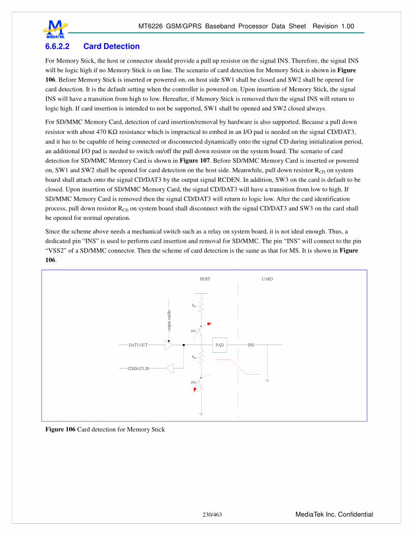
MT6226 GSM/GPRS Baseband Processor Data Sheet Revision 1.00
230/463 MediaTek Inc. Confidential
6.6.2.2 Card Detection
For Memory Stick, the host or connector should provide a pull up resistor on the signal INS. Therefore, the signal INS will be logic high if no Memory Stick is on line. The scenario of card detection for Memory Stick is shown in Figure 106. Before Memory Stick is inserted or powered on, on host side SW1 shall be closed and SW2 shall be opened for card detection. It is the default setting when the controller is powered on. Upon insertion of Memory Stick, the signal INS will have a transition from high to low. Hereafter, if Memory Stick is removed then the signal INS will return to logic high. If card insertion is intended to not be supported, SW1 shall be opened and SW2 closed always.
For SD/MMC Memory Card, detection of card insertion/removal by hardware is also supported. Because a pull down
resistor with about 470 KΩ resistance which is impractical to embed in an I/O pad is needed on the signal CD/DAT3, and it has to be capable of being connected or disconnected dynamically onto the signal CD during initialization period, an additional I/O pad is needed to switch on/off the pull down resistor on the system board. The scenario of card detection for SD/MMC Memory Card is shown in Figure 107. Before SD/MMC Memory Card is inserted or powered on, SW1 and SW2 shall be opened for card detection on the host side. Meanwhile, pull down resistor RCD on system board shall attach onto the signal CD/DAT3 by the output signal RCDEN. In addition, SW3 on the card is default to be closed. Upon insertion of SD/MMC Memory Card, the signal CD/DAT3 will have a transition from low to high. If SD/MMC Memory Card is removed then the signal CD/DAT3 will return to logic low. After the card identification process, pull down resistor RCD on system board shall disconnect with the signal CD/DAT3 and SW3 on the card shall be opened for normal operation.
Since the scheme above needs a mechanical switch such as a relay on system board, it is not ideal enough. Thus, a dedicated pin “INS” is used to perform card insertion and removal for SD/MMC. The pin “INS” will connect to the pin “VSS2” of a SD/MMC connector. Then the scheme of card detection is the same as that for MS. It is shown in Figure 106.
Figure 106 Card detection for Memory Stick

MT6226 GSM/GPRS Baseband Processor Data Sheet Revision 1.00
231/463 MediaTek Inc. Confidential
Figure 107 Card detection for SD/MMC Memory Card

MT6226 GSM/GPRS Baseband Processor Data Sheet Revision 1.00
232/463 MediaTek Inc. Confidential
6.6.3 Register Definitions
REGISTER ADDRESS REGISTER NAME SYNONYM
MSDC + 0000h MS/SD Memory Card Controller Configuration Register MSDC_CFG
MSDC + 0004h MS/SD Memory Card Controller Status Register MSDC_STA
MSDC + 0008h MS/SD Memory Card Controller Interrupt Register MSDC_INT
MSDC + 000Ch MS/SD Memory Card Controller Data Register MSDC_DAT
MSDC + 00010h MS/SD Memory Card Pin Status Register MSDC_PS
MSDC + 00014h MS/SD Memory Card Controller IO Control Register MSDC_IOCON
MSDC + 0020h SD Memory Card Controller Configuration Register SDC_CFG
MSDC + 0024h SD Memory Card Controller Command Register SDC_CMD
MSDC + 0028h SD Memory Card Controller Argument Register SDC_ARG
MSDC + 002Ch SD Memory Card Controller Status Register SDC_STA
MSDC + 0030h SD Memory Card Controller Response Register 0 SDC_RESP0
MSDC + 0034h SD Memory Card Controller Response Register 1 SDC_RESP1
MSDC + 0038h SD Memory Card Controller Response Register 2 SDC_RESP2
MSDC + 003Ch SD Memory Card Controller Response Register 3 SDC_RESP3
MSDC + 0040h SD Memory Card Controller Command Status Register SDC_CMDSTA
MSDC + 0044h SD Memory Card Controller Data Status Register SDC_DATSTA
MSDC + 0048h SD Memory Card Status Register SDC_CSTA
MSDC + 004Ch SD Memory Card IRQ Mask Register 0 SDC_IRQMASK0
MSDC + 0050h SD Memory Card IRQ Mask Register 1 SDC_IRQMASK1
MSDC + 0054h SDIO Configuration Register SDIO_CFG
MSDC + 0058h SDIO Status Register SDIO_STA
MSDC + 0060h Memory Stick Controller Configuration Register MSC_CFG
MSDC + 0064h Memory Stick Controller Command Register MSC_CMD
MSDC + 0068h Memory Stick Controller Auto Command Register MSC_ACMD
MSDC + 006Ch Memory Stick Controller Status Register MSC_STA
Table 42 MS/SD Controller Register Map
6.6.3.1 Global Register Definitions
MSDC+0000h MS/SD Memory Card Controller Configuration Register
MSDC_CFG
Bit 31 30 29 28 27 26 25 24 23 22 21 20 19 18 17 16
Name FIFOTHD PRCFG2 PRCFG1 PRCFG0 VDDPD
RCDEN
DIRQEN
PINEN
DMAEN
INTEN
Type R/W R/W R/W R/W R/W R/W R/W R/W R/W R/W Reset 0001 01 01 10 0 0 0 0 0 0
Bit 15 14 13 12 11 10 9 8 7 6 5 4 3 2 1 0
Name SCLKF SCLKON CRED STDB
Y CLKS
RC RST NOCRC RED MSD
C Type R/W R/W R/W R/W R/W W R/W R/W R/W Reset 00000000 0 0 1 0 0 0 0 0

MT6226 GSM/GPRS Baseband Processor Data Sheet Revision 1.00
233/463 MediaTek Inc. Confidential
The register is for general configuration of the MS/SD controller. Note that MSDC_CFG[31:16] can be accessed by 16-bit APB bus access.
MSDC The register bit is used to configure the controller as the host of Memory Stick or as the host of SD/MMC Memory card. The default value is to configure the controller as the host of Memory Stick. 0 Configure the controller as the host of Memory Stick 1 Configure the controller as the host of SD/MMC Memory card
RED Rise Edge Data. The register bit is used to determine that serial data input is latched at the falling edge or the rising edge of serial clock. The default setting is at the rising edge. If serial data has worse timing, set the register bit to ‘1’. When memory card has worse timing on return read data, set the register bit to ‘1’. 0 Serial data input is latched at the rising edge of serial clock. 1 Serial data input is latched at the falling edge of serial clock.
NOCRC CRC Disable. A ‘1’ indicates that data transfer without CRC is desired. For write data block, data will be transmitted without CRC. For read data block, CRC will not be checked. It is for testing purpose. 0 Data transfer with CRC is desired. 1 Data transfer without CRC is desired.
RST Software Reset. Writing a ‘1’ to the register bit will cause internal synchronous reset of MS/SD controller, but does not reset register settings. 0 Otherwise 1 Reset MS/SD controller
CLKSRC The register bit specifies which clock is used as source clock of memory card. If MUC clock is used, the fastest clock rate for memory card is 52/2=26MHz. If USB clock is used, the fastest clock rate for memory card is 48/2=24MHz. 0 Use MCU clock as source clock of memory card. 1 Use USB clock as source clock of memory card.
STDBY Standby Mode. If the module is powered down, operating clock to the module will be stopped. At the same time, clock to card detection circuitry will also be stopped. If detection of memory card insertion and removal is desired, write ‘1’ to the register bit. If interrupt for detection of memory card insertion and removal is enabled, interrupt will take place whenever memory is inserted or removed. 0 Standby mode is disabled. 1 Standby mode is enabled.
CRED Card Rise Edge Data. The register bit is used to determine that serial data from memory card is output at the falling edge or the rising edge of serial clock. The default setting is at the falling edge. 0 Serial data is output at the falling edge of serial clock. 1 Serial data is output at the rising edge of serial clock.
SCLKON Serial Clock Always On. It is for debugging purpose. 0 Not to have serial clock always on. 1 To have serial clock always on.
SCLKF The register field controls clock frequency of serial clock on MS/SD bus. Denote clock frequency of MS/SD bus serial clock as fslave and clock frequency of the MS/SD controller as fhost which is 104 or 52 MHz. Then the value of the register field is as follows. Note that the allowable maximum frequency of fslave is 26MHz. 00000000b fslave =(1/2) * fhost 00000001b fslave = (1/(4*1)) * fhost
00000010b fslave = (1/(4*2)) * fhost
00000011b fslave = (1/(4*3))* fhost
… 00010000b fslave = (1/(4*16))* fhost
…

MT6226 GSM/GPRS Baseband Processor Data Sheet Revision 1.00
234/463 MediaTek Inc. Confidential
11111111b fslave = (1/(4*255)) * fhost
INTEN Interrupt Enable. Note that if interrupt capability is disabled then application software must poll the status of the register MSDC_STA to check for any interrupt request. 0 Interrupt induced by various conditions is disabled, no matter the controller is configured as the host of
either SD/MMC Memory Card or Memory Stick. 1 Interrupt induced by various conditions is enabled, no matter the controller is configured as the host of
either SD/MMC Memory Card or Memory Stick. DMAEN DMA Enable. Note that if DMA capability is disabled then application software must poll the status of the
register MSDC_STA for checking any data transfer request. If DMA is desired, the register bit must be set before command register is written. 0 DMA request induced by various conditions is disabled, no matter the controller is configured as the host
of either SD/MMC Memory Card or Memory Stick. 1 DMA request induced by various conditions is enabled, no matter the controller is configured as the host
of either SD/MMC Memory Card or Memory Stick. PINEN Pin Interrupt Enable. The register bit is used to control if the pin for card detection is used as an interrupt
source. 0 The pin for card detection is not used as an interrupt source. 1 The pin for card detection is used as an interrupt source.
DIRQEN Data Request Interrupt Enable. The register bit is used to control if data request is used as an interrupt source. 0 Data request is not used as an interrupt source. 1 Data request is used as an interrupt source.
RCDEN The register bit controls the output pin RCDEN that is used for card identification process when the controller is for SD/MMC Memory Card. Its output will control the pull down resistor on the system board to connect or disconnect with the signal CD/DAT3. 0 The output pin RCDEN will output logic low. 1 The output pin RCDEN will output logic high.
VDDPD The register bit controls the output pin VDDPD that is used for power saving. The output pin VDDPD will control power for memory card. 0 The output pin VDDPD will output logic low. The power for memory card will be turned off. 1 The output pin VDDPD will output logic high. The power for memory card will be turned on.
PRCFG0 Pull Up/Down Register Configuration for the pin WP. The default value is 10. 00 Pull up resistor and pull down resistor in the I/O pad of the pin WP are all disabled. 01 Pull down resistor in the I/O pad of the pin WP is enabled. 10 Pull up resistor in the I/O pad of the pin WP is enabled. 11 Use keeper of IO pad.
PRCFG1 Pull Up/Down Register Configuration for the pin CMD/BS. The default value is 0b01. 00 Pull up resistor and pull down resistor in the I/O pad of the pin CMD/BS are all disabled. 01 Pull down resistor in the I/O pad of the pin CMD/BS is enabled. 10 Pull up resistor in the I/O pad of the pin CMD/BS is enabled. 11 Use keeper of IO pad.
PRCFG2 Pull Up/Down Register Configuration for the pins DAT0, DAT1, DAT2, DAT3. The default value is 0b01. 00 Pull up resistor and pull down resistor in the I/O pads o the pins DAT0, DAT1, DAT2, DAT3. are all
disabled.

MT6226 GSM/GPRS Baseband Processor Data Sheet Revision 1.00
235/463 MediaTek Inc. Confidential
01 Pull down resistor in the I/O pads of the pins DAT0, DAT1, DAT2, DAT3 and WP. is enabled. 10 Pull up resistor in the I/O pads of the pins DAT0, DAT1, DAT2, DAT3. is enabled. 11 Use keeper of IO pad.
FIFOTHD FIFO Threshold. The register field determines when to issue a DMA request. For write transactions, DMA requests will be asserted if the number of free entries in FIFO are larger than or equal to the value in the register field. For read transactions, DMA requests will be asserted if the number of valid entries in FIFO are larger than or equal to the value in the register field. The register field must be set according to the setting of data transfer count in DMA burst mode. If single mode for DMA transfer is used, the register field shall be set to 0b0001. 0000 Invalid. 0001 Threshold value is 1. 0010 Threshold value is 2. … 1000 Threshold value is 8. others Invalid
MSDC+0004h MS/SD Memory Card Controller Status Register MSDC_STA Bit 15 14 13 12 11 10 9 8 7 6 5 4 3 2 1 0
Name BUSY FIFOCLR FIFOCNT INT DRQ BE BF
Type R W RO RO RO RO RO Reset 0 - 0000 0 0 0 0
The register contains the status of FIFO, interrupts and data requests.
BF The register bit indicates if FIFO in MS/SD controller is full. 0 FIFO in MS/SD controller is not full. 1 FIFO in MS/SD controller is full.
BE The register bit indicates if FIFO in MS/SD controller is empty. 0 FIFO in MS/SD controller is not empty. 1 FIFO in MS/SD controller is empty.
DRQ The register bit indicates if any data transfer is required. While any data transfer is required, the register bit still will be active even if the register bit DIRQEN in the register MSDC_CFG is disabled. Data transfer can be achieved by DMA channel alleviating MCU loading, or by polling the register bit to check if any data transfer is requested. While the register bit DIRQEN in the register MSDC_CFG is disabled, the second method is used. 0 No DMA request exists. 1 DMA request exists.
INT The register bit indicates if any interrupt exists. While any interrupt exists, the register bit still will be active even if the register bit INTEN in the register MSDC_CFG is disabled. MS/SD controller can interrupt MCU by issuing interrupt request to Interrupt Controller, or software/application polls the register endlessly to check if any interrupt request exists in MS/SD controller. While the register bit INTEN in the register MSDC_CFG is disabled, the second method is used. For read commands, it is possible that timeout error takes place. Software can read the status register to check if timeout error takes place without OS time tick support or data request is asserted. Note that the register bit will be cleared when reading the register MSDC_INT. 0 No interrupt request exists. 1 Interrupt request exists.
FIFOCNT FIFO Count. The register field shows how many valid entries are in FIFO. 0000 There is 0 valid entry in FIFO. 0001 There is 1 valid entry in FIFO.

MT6226 GSM/GPRS Baseband Processor Data Sheet Revision 1.00
236/463 MediaTek Inc. Confidential
0010 There are 2 valid entries in FIFO. … 1000 There are 8 valid entries in FIFO. others Invalid
FIFOCLR Clear FIFO. Writing ‘1’ to the register bit will cause the content of FIFO clear and reset the status of FIFO controller. 0 No effect on FIFO. 1 Clear the content of FIFO clear and reset the status of FIFO controller.
BUSY Status of the controller. If the controller is in busy state, the register bit will be ‘1’. Otherwise ‘0’. 0 The controller is in busy state. 1 The controller is in idle state.
MSDC+0008h MS/SD Memory Card Controller Interrupt Register MSDC_INT Bit 15 14 13 12 11 10 9 8 7 6 5 4 3 2 1 0
Name SDIOIRQ
SDR1BIRQ
MSIFIRQ
SDMCIRQ
SDDATIRQ
SDCMDIRQ
PINIRQ DIRQ
Type RC RC RC RC RC RC RC RC Reset 0 0 0 0 0 0 0 0
The register contains the status of interrupts. Note that the register still show status of interrupt even though interrupt is disabled, that is, the register bit INTEN of the register MSDC_CFG is set to ‘0. It implies that software interrupt can be implemented by polling the register bit INT of the register MSDC_STA and this register. However, if hardware interrupt is desired, remember to clear the register before setting the register bit INTEN of the register MSDC_CFG to ‘1’. Or undesired hardware interrupt arisen from previous interrupt status may take place.
DIRQ Data Request Interrupt. The register bit indicates if any interrupt for data request exists. Whenever data request exists and data request as an interrupt source is enabled, i.e., the register bit DIRQEN in the register MSDC_CFG is set to ‘1’, the register bit will be active. It will be reset when reading it. For software, data requests can be recognized by polling the register bit DRQ or by data request interrupt. Data request interrupts will be generated every FIFOTHD data transfers. 0 No Data Request Interrupt. 1 Data Request Interrupt occurs.
PINIRQ Pin Change Interrupt. The register bit indicates if any interrupt for memory card insertion/removal exists. Whenever memory card is inserted or removed and card detection interrupt is enabled, i.e., the register bit PINEN in the register MSDC_CFG is set to ‘1’, the register bit will be set to ‘1’. It will be reset when the register is read. 0 Otherwise. 1 Card is inserted or removed.
SDCMDIRQ SD Bus CMD Interrupt. The register bit indicates if any interrupt for SD CMD line exists. Whenever interrupt for SD CMD line exists, i.e., any bit in the register SDC_CMDSTA is active, the register bit will be set to ‘1’ if interrupt is enabled. It will be reset when the register is read. 0 No SD CMD line interrupt. 1 SD CMD line interrupt exists.
SDDATIRQ SD Bus DAT Interrupt. The register bit indicates if any interrupt for SD DAT line exists. Whenever interrupt for SD DAT line exists, i.e., any bit in the register SDC_ DATSTA is active, the register bit will be set to ‘1’ if interrupt is enabled. It will be reset when the register is read. 0 No SD DAT line interrupt. 1 SD DAT line interrupt exists.

MT6226 GSM/GPRS Baseband Processor Data Sheet Revision 1.00
237/463 MediaTek Inc. Confidential
SDMCIRQ SD Memory Card Interrupt. The register bit indicates if any interrupt for SD Memory Card exists. Whenever interrupt for SD Memory Card exists, i.e., any bit in the register SDC_CSTA is active, the register bit will be set to ‘1’ if interrupt is enabled. It will be reset when the register is read. 0 No SD Memory Card interrupt. 1 SD Memory Card interrupt exists.
MSIFIRQ MS Bus Interface Interrupt. The register bit indicates if any interrupt for MS Bus Interface exists. Whenever interrupt for MS Bus Interface exists, i.e., any bit in the register MSC_STA is active, the register bit will be set to ‘1’ if interrupt is enabled. It will be reset when the register MSDC_STA or MSC_STA is read. 0 No MS Bus Interface interrupt. 1 MS Bus Interface interrupt exists.
SDR1BIRQ SD/MMC R1b Response Interrupt. The register bit will be active when a SD/MMC command with R1b response finishes and the DAT0 line has transition from busy to idle state. Single block write commands with R1b response will cause the interrupt when the command completes no matter successfully or with CRC error. However, multi-block write commands with R1b response do not cause the interrupt because multi-block write commands are always stopped by STOP_TRANS commands. STOP_TRANS commands (with R1b response) behind multi-block write commands will cause the interrupt. Single block read command with R1b response will cause the interrupt when the command completes but multi-block read commands do not. Note that STOP_TRANS commands (with R1b response) behind multi-block read commands will cause the interrupt.
0 No interrupt for SD/MMC R1b response. 1 Interrupt for SD/MMC R1b response exists.
MSDC+000Ch MS/SD Memory Card Controller Data Register MSDC_DAT Bit 31 30 29 28 27 26 25 24 23 22 21 20 19 18 17 16
Name DATA[31:16] Type R/W Bit 15 14 13 12 11 10 9 8 7 6 5 4 3 2 1 0
Name DATA[15:0] Type R/W
The register is used to read/write data from/to FIFO inside MS/SD controller. Data access is in unit of 32 bits.
MSDC+0010h MS/SD Memory Card Pin Status Register MSDC_PS Bit 31 30 29 28 27 26 25 24 23 22 21 20 19 18 17 16
Name CMD DAT Type RO RO Reset - -
Bit 15 14 13 12 11 10 9 8 7 6 5 4 3 2 1 0
Name CDDEBOUNCE PINCHG PIN0 POEN
0 PIEN0 CDEN
Type RW RC RO R/W R/W R/W Reset 0000 0 1 0 0 0
The register is used for card detection. When the memory card controller is powered on, and the system is powered on, the power for the memory card is still off unless power has been supplied by the PMIC. Meanwhile, pad for card detection defaults to pull down when the system is powered on. The scheme of card detection for MS is the same as that for SD/MMC.
For detecting card insertion, first pull up INS pin, and then enable card detection and input pin at the same time. After 32 cycles of controller clock, status of pin changes will emerge. For detecting card removal, just keep enabling card detection and input pin.
CDEN Card Detection Enable. The register bit is used to enable or disable card detection.

MT6226 GSM/GPRS Baseband Processor Data Sheet Revision 1.00
238/463 MediaTek Inc. Confidential
0 Card detection is disabled. 1 Card detection is enabled.
PIEN0 The register bit is used to control input pin for card detection. 0 Input pin for card detection is disabled. 1 Input pin for card detection is enabled.
POEN0 The register bit is used to control output of input pin for card detection. 0 Output of input pin for card detection is disabled. 1 Output of input pin for card detection is enabled.
PIN0 The register shows the value of input pin for card detection. 0 The value of input pin for card detection is logic low. 1 The value of input pin for card detection is logic high.
PINCHG Pin Change. The register bit indicates the status of card insertion/removal. If memory card is inserted or removed, the register bit will be set to ‘1’ no matter pin change interrupt is enabled or not. It will be cleared when the register is read. 0 Otherwise. 1 Card is inserted or removed.
CDDEBOUNCE The register field specifies the time interval for card detection de-bounce. Its default value is 0. It means that de-bounce interval is 32 cycle time of 32KHz. The interval will extend one cycle time of 32KHz by increasing the counter by 1.
DAT Memory Card Data Lines. CMD Memory Card Command Lines.
MSDC+0014h MS/SD Memory Card Controller IO Control Register MSDC_IOCON Bit 15 14 13 12 11 10 9 8 7 6 5 4 3 2 1 0
Name PRCFG3 SRCFG1
SRCFG0 ODCCFG1 ODCCFG0
Type R/W R/W R/W R/W R/W Reset 10 1 1 000 011
The register specifies Output Driving Capability and Slew Rate of IO pads for MSDC. The reset value is suggestion setting. If output driving capability of the pins DAT0, DAT1, DAT2 and DAT3 is too large, it’s possible to arise ground bounce and thus result in glitch on SCLK.
ODCCFG0 Output driving capability the pins CMD/BS and SCLK 000 2mA 001 4mA 010 6mA 011 8mA 100 10mA 101 12mA 110 14mA 111 16mA
ODCCFG1 Output driving capability the pins DAT0, DAT1, DAT2 and DAT3 000 2mA 001 4mA 010 6mA 011 8mA 100 10mA 101 12mA 110 14mA

MT6226 GSM/GPRS Baseband Processor Data Sheet Revision 1.00
239/463 MediaTek Inc. Confidential
111 16mA SRCFG0 Output driving capability the pins CMD/BS and SCLK
0 Fast Slew Rate 1 Slow Slew Rate
SRCFG1 Output driving capability the pins DAT0, DAT1, DAT2 and DAT3 0 Fast Slew Rate 1 Slow Slew Rate
PRCFG3 Pull Up/Down Register Configuration for the pin INS. The default value is 10. 00 Pull up resistor and pull down resistor in the I/O pad of the pin INS are all disabled. 01 Pull down resistor in the I/O pad of the pin INS is enabled. 10 Pull up resistor in the I/O pad of the pin INS is enabled. 11 Use keeper of IO pad.
6.6.3.2 SD Memory Card Controller Register Definitions
MSDC+0020h SD Memory Card Controller Configuration Register SDC_CFG Bit 31 30 29 28 27 26 25 24 23 22 21 20 19 18 17 16
Name DTOC WDOD SDIO MDLW8
MDLEN SIEN
Type R/W R/W R/W R/W R/W R/W Reset 00000000 0000 0 0 0 0
Bit 15 14 13 12 11 10 9 8 7 6 5 4 3 2 1 0 Name BSYDLY BLKLEN Type R/W R/W Reset 1000 00000000000
The register is used for configuring the MS/SD Memory Card Controller when it is configured as the host of SD Memory Card. If the controller is configured as the host of Memory Stick, the contents of the register have no impact on the operation of the controller. Note that SDC_CFG[31:16] can be accessed by 16-bit APB bus access.
BLKLEN It refers to Block Length. The register field is used to define the length of one block in unit of byte in a data transaction. The maximal value of block length is 2048 bytes.
000000000000 Reserved. 000000000001 Block length is 1 byte. 000000000010 Block length is 2 bytes. … 011111111111 Block length is 2047 bytes. 100000000000 Block length is 2048 bytes.
BSYDLY The register field is only valid for the commands with R1b response. If the command has a response of R1b type, MS/SD controller must monitor the data line 0 for card busy status from the bit time that is two serial clock cycles after the command end bit to check if operations in SD/MMC Memory Card have finished. The register field is used to expand the time between the command end bit and end of detection period to detect card busy status. If time is up and there is no card busy status on data line 0, then the controller will abandon the detection. 0000 No extend. 0001 Extend one more serial clock cycle. 0010 Extend two more serial clock cycles. … 1111 Extend fifteen more serial clock cycle.
SIEN Serial Interface Enable. It should be enabled as soon as possible before any command.

MT6226 GSM/GPRS Baseband Processor Data Sheet Revision 1.00
240/463 MediaTek Inc. Confidential
0 Serial interface for SD/MMC is disabled. 1 Serial interface for SD/MMC is enabled.
MDLW8 Eight Data Line Enable. The register works when MDLEN is enabled. The register can be enabled only when MultiMediaCard 4.0 is applied and detected by software application.
0 4-bit Data line is enabled. 1 8-bit Data line is enabled.
SDIO SDIO Enable. 0 SDIO mode is disabled 1 SDIO mode is enabled
MDLEN Multiple Data Line Enable. The register can be enabled only when SD Memory Card is applied and detected by software application. It is the responsibility of the application to program the bit correctly when an MultiMediaCard is applied. If an MultiMediaCard is applied and 4-bit data line is enabled, then 4 bits will be output every serial clock. Therefore, data integrity will fail. 0 4-bit Data line is disabled. 1 4-bit Data line is enabled.
WDOD Write Data Output Delay. The period from finish of the response for the initial host write command or the last write data block in a multiple block write operation to the start bit of the next write data block requires at least two serial clock cycles. The register field is used to extend the period (Write Data Output Delay) in unit of one serial clock. 0000 No extend. 0001 Extend one more serial clock cycle. 0010 Extend two more serial clock cycles. … 1111 Extend fifteen more serial clock cycle.
DTOC Data Timeout Counter. The period from finish of the initial host read command or the last read data block in a multiple block read operation to the start bit of the next read data block requires at least two serial clock cycles. The counter is used to extend the period (Read Data Access Time) in unit of 65,536 serial clock. See the register field description of the register bit RDINT for reference. 00000000 Extend 65,536 more serial clock cycle. 00000001 Extend 65,536x2 more serial clock cycle. 00000010 Extend 65,536x3 more serial clock cycle. … 11111111 Extend 65,536x 256 more serial clock cycle.
MSDC+0024h SD Memory Card Controller Command Register SDC_CMD Bit 31 30 29 28 27 26 25 24 23 22 21 20 19 18 17 16
Name CMDFAIL
Type R/W Reset 0
Bit 15 14 13 12 11 10 9 8 7 6 5 4 3 2 1 0
Name INTC STOP RW DTYPE IDRT RSPTYP BREAK CMD
Type R/W R/W R/W R/W R/W R/W R/W R/W Reset 0 0 0 00 0 000 0 000000
The register defines a SD Memory Card command and its attribute. Before MS/SD controller issues a transaction onto SD bus, application shall specify other relative setting such as argument for command. After application writes the register, MS/SD controller will issue the corresponding transaction onto SD serial bus. If the command is GO_IDLE_STATE, the controller will have serial clock on SD/MMC bus run 128 cycles before issuing the command.

MT6226 GSM/GPRS Baseband Processor Data Sheet Revision 1.00
241/463 MediaTek Inc. Confidential
CMD SD Memory Card command. It is totally 6 bits. BREAK Abort a pending MMC GO_IRQ_MODE command. It is only valid for a pending GO_IRQ_MODE command
waiting for MMC interrupt response. 0 Other fields are valid. 1 Break a pending MMC GO_IRQ_MODE command in the controller. Other fields are invalid.
RSPTYP The register field defines response type for the command. For commands with R1 and R1b response, the register SDC_CSTA (not SDC_STA) will update after response token is received. This register SDC_CSTA contains the status of the SD/MMC and it will be used as response interrupt sources. Note that if CMD7 is used with all 0’s RCA then RSPTYP must be “000”. And the command “GO_TO_IDLE” also have RSPTYP=’000’. 000 There is no response for the command. For instance, broadcast command without response and
GO_INACTIVE_STATE command. 001 The command has R1 response. R1 response token is 48-bit. 010 The command has R2 response. R2 response token is 136-bit. 011 The command has R3 response. Even though R3 is 48-bit response, but it does not contain CRC
checksum. 100 The command has R4 response. R4 response token is 48-bit. (Only for MMC) 101 The command has R5 response. R5 response token is 48-bit. (Only for MMC) 110 The command has R6 response. R6 response token is 48-bit. 111 The command has R1b response. If the command has a response of R1b type, MS/SD controller must
monitor the data line 0 for card busy status from the bit time that is two or four serial clock cycles after the command end bit to check if operations in SD/MMC Memory Card have finished. There are two cases for detection of card busy status. The first case is that the host stops the data transmission during an active write data transfer. The card will assert busy signal after the stop transmission command end bit followed by four serial clock cycles. The second case is that the card is in idle state or under a scenario of receiving a stop transmission command between data blocks when multiple block write command is in progress. The register bit is valid only when the command has a response token.
Note that the response type R4 and R5 mentioned above is for MMC only. For SDIO, RSPTYP definition is different and shall be set to : 001 (i) CMD5 of SDIO is to be issued. (Where the response is defined as R4 in SDIO spec)
(ii) CMD52 or CMD53 for READ is to be issued. (Where the response is defined as R5 in SDIO spec)
111 CMD52 for I/O abort or CMD53 for WRITE is to be issued (Where the response is defined as R5 in SDIO spec)
IDRT Identification Response Time. The register bit indicates if the command has a response with NID (that is, 5 serial clock cycles as defined in SD Memory Card Specification Part 1 Physical Layer Specification version 1.0) response time. The register bit is valid only when the command has a response token. Thus the register bit must be set to ‘1’ for CMD2 (ALL_SEND_CID) and ACMD41 (SD_APP_OP_CMD). 0 Otherwise. 1 The command has a response with NID response time.
DTYPE The register field defines data token type for the command. 00 No data token for the command 01 Single block transaction 10 Multiple block transaction. That is, the command is a multiple block read or write command. 11 Stream operation. It only shall be used when an MultiMediaCard is applied.
RW The register bit defines the command is a read command or write command. The register bit is valid only when the command will cause a transaction with data token.

MT6226 GSM/GPRS Baseband Processor Data Sheet Revision 1.00
242/463 MediaTek Inc. Confidential
0 The command is a read command. 1 The command is a write command.
STOP The register bit indicates if the command is a stop transmission command. It should be set to 1 when CMD12 (SD/MMC) or CMD52 with I/O abort (SDIO) is to be issued. 0 The command is not a stop transmission command. 1 The command is a stop transmission command.
INTC The register bit indicates if the command is GO_IRQ_STATE. If the command is GO_IRQ_STATE, the period between command token and response token will not be limited. 0 The command is not GO_IRQ_STATE. 1 The command is GO_IRQ_STATE.
CMDFAIL The register bit is used for controlling SDIO interrupt period when CRC error or Command/Data timeout condition occurs. It is useful only when SDIO 4-bit mode is activated. 0 SDIO Interrupt period will re-start after a stop command (CMD12) or I/O abort command (CMD52) is
issued. 1 SDIO Interrupt period will re-start whenever DAT line is not busy.
MSDC+0028h SD Memory Card Controller Argument Register SDC_ARG Bit 31 30 29 28 27 26 25 24 23 22 21 20 19 18 17 16
Name ARG [31:16] Type R/W Bit 15 14 13 12 11 10 9 8 7 6 5 4 3 2 1 0
Name ARG [15:0] Type R/W
The register contains the argument of the SD/MMC Memory Card command.
MSDC+002Ch SD Memory Card Controller Status Register SDC_STA Bit 15 14 13 12 11 10 9 8 7 6 5 4 3 2 1 0
Name WP R1BSY RSV DATB
USY CMDBUSY
SDCBUSY
Type R RO RO RO RO RO Reset - 0 0 0 0 0
The register contains various status of MS/SD controller as the controller is configured as the host of SD Memory Card.
SDCBUSY The register field indicates if MS/SD controller is busy, that is, any transmission is going on CMD or DAT line on SD bus. 0 MS/SD controller is idle. 1 MS/SD controller is busy.
CMDBUSY The register field indicates if any transmission is going on CMD line on SD bus. 0 No transmission is going on CMD line on SD bus. 1 There exists transmission going on CMD line on SD bus.
DATBUSY The register field indicates if any transmission is going on DAT line on SD bus. For those commands without data but still involving DAT line, the register bit is useless. For example, if an Erase command is issued, then checking if the register bit is ‘0’ before issuing next command with data would not guarantee that the controller is idle. In this situation, use the register bit SDCBUSY. 0 No transmission is going on DAT line on SD bus. 1 There exists transmission going on DAT line on SD bus.
R1BSY The register field shows the status of DAT line 0 for commands with R1b response. 0 SD/MMC Memory card is not busy. 1 SD/MMC Memory card is busy.

MT6226 GSM/GPRS Baseband Processor Data Sheet Revision 1.00
243/463 MediaTek Inc. Confidential
WP It is used to detect the status of Write Protection Switch on SD Memory Card. The register bit shows the status of Write Protection Switch on SD Memory Card. There is no default reset value. The pin WP (Write Protection) is also only useful while the controller is configured for SD Memory Card. 1 Write Protection Switch ON. It means that memory card is desired to be write-protected. 0 Write Protection Switch OFF. It means that memory card is writable.
MSDC+0030h SD Memory Card Controller Response Register 0 SDC_RESP0 Bit 31 30 29 28 27 26 25 24 23 22 21 20 19 18 17 16
Name RESP [31:16] Type RO Bit 15 14 13 12 11 10 9 8 7 6 5 4 3 2 1 0
Name RESP [15:0] Type RO
The register contains parts of the last SD/MMC Memory Card bus response. See description for the register field SDC_RESP3.
MSDC+0034h SD Memory Card Controller Response Register 1 SDC_RESP1 Bit 31 30 29 28 27 26 25 24 23 22 21 20 19 18 17 16
Name RESP [63:48] Type RO Bit 15 14 13 12 11 10 9 8 7 6 5 4 3 2 1 0
Name RESP [47:32] Type RO
The register contains parts of the last SD/MMC Memory Card bus response. See description for the register field SDC_RESP3.
MSDC+0038h SD Memory Card Controller Response Register 2 SDC_RESP2 Bit 31 30 29 28 27 26 25 24 23 22 21 20 19 18 17 16
Name RESP [95:80] Type RO Bit 15 14 13 12 11 10 9 8 7 6 5 4 3 2 1 0
Name RESP [79:64] Type RO
The register contains parts of the last SD/MMC Memory Card bus response. See description for the register field SDC_RESP3.
MSDC+003Ch SD Memory Card Controller Response Register 3 SDC_RESP3 Bit 31 30 29 28 27 26 25 24 23 22 21 20 19 18 17 16
Name RESP [127:112] Type RO Bit 15 14 13 12 11 10 9 8 7 6 5 4 3 2 1 0
Name RESP [111:96] Type RO
The register contains parts of the last SD/MMC Memory Card bus response. The register fields SDC_RESP0, SDC_RESP1, SDC_RESP2 and SDC_RESP3 compose the last SD/MMC Memory card bus response. For response of type R2, that is, response of the command ALL_SEND_CID, SEND_CSD and SEND_CID, only bit 127 to 0 of response token is stored in the register field SDC_RESP0, SDC_RESP1, SDC_RESP2 and SDC_RESP3. For response of other types, only bit 39 to 8 of response token is stored in the register field SDC_RESP0.

MT6226 GSM/GPRS Baseband Processor Data Sheet Revision 1.00
244/463 MediaTek Inc. Confidential
MSDC+0040h SD Memory Card Controller Command Status Register
SDC_CMDSTA
Bit 15 14 13 12 11 10 9 8 7 6 5 4 3 2 1 0
Name MMCIRQ
RSPCRCER
R
CMDTO
CMDRDY
Type RC RC RC RC Reset 0 0 0 0
The register contains the status of MS/SD controller during command execution and that of MS/SD bus protocol after command execution when MS/SD controller is configured as the host of SD/MMC Memory Card. The register will also be used as interrupt sources. The register will be cleared when reading the register. Meanwhile, if interrupt is enabled and thus interrupt caused by the register is generated, reading the register will deassert the interrupt.
CMDRDY For command without response, the register bit will be ‘1’ once the command completes on SD/MMC bus. For command with response, the register bit will be ‘1’ whenever the command is issued onto SD/MMC bus and its corresponding response is received without CRC error. 0 Otherwise. 1 Command with/without response finish successfully without CRC error.
CMDTO Timeout on CMD detected. A ‘1’ indicates that MS/SD controller detected a timeout condition while waiting for a response on the CMD line. 0 Otherwise. 1 MS/SD controller detected a timeout condition while waiting for a response on the CMD line.
RSPCRCERR CRC error on CMD detected. A ‘1’ indicates that MS/SD controller detected a CRC error after reading a response from the CMD line. 0 Otherwise. 1 MS/SD controller detected a CRC error after reading a response from the CMD line.
MMCIRQ MMC requests an interrupt. A ‘1’ indicates that a MMC supporting command class 9 issued an interrupt request. 0 Otherwise. 1 A ‘1’ indicates that a MMC supporting command class 9 issued an interrupt request.
MSDC+0044h SD Memory Card Controller Data Status Register SDC_DATSTA Bit 15 14 13 12 11 10 9 8 7 6 5 4 3 2 1 0
Name DATCRCER
R
DATTO
BLKDONE
Type RC RC RC Reset 0 0 0
The register contains the status of MS/SD controller during data transfer on DAT line(s) when MS/SD controller is configured as the host of SD/MMC Memory Card. The register also will be used as interrupt sources. The register will be cleared when reading the register. Meanwhile, if interrupt is enabled and thus interrupt caused by the register is generated, reading the register will deassert the interrupt.
BLKDONE The register bit indicates the status of data block transfer. 0 Otherwise. 1 A data block was successfully transferred.
DATTO Timeout on DAT detected. A ‘1’ indicates that MS/SD controller detected a timeout condition while waiting for data token on the DAT line. 0 Otherwise. 1 MS/SD controller detected a timeout condition while waiting for data token on the DAT line.

MT6226 GSM/GPRS Baseband Processor Data Sheet Revision 1.00
245/463 MediaTek Inc. Confidential
DATCRCERR CRC error on DAT detected. A ‘1’ indicates that MS/SD controller detected a CRC error after reading a block of data from the DAT line or SD/MMC signaled a CRC error after writing a block of data to the DAT line. 0 Otherwise. 1 MS/SD controller detected a CRC error after reading a block of data from the DAT line or SD/MMC
signaled a CRC error after writing a block of data to the DAT line.
MSDC+0048h SD Memory Card Status Register SDC_CSTA Bit 31 30 29 28 27 26 25 24 23 22 21 20 19 18 17 16
Name CSTA [31:16] Type RC Reset 0000000000000000
Bit 15 14 13 12 11 10 9 8 7 6 5 4 3 2 1 0 Name CSTA [15:0] Type RC Reset 0000000000000000
After commands with R1 and R1b response this register contains the status of the SD/MMC card and it will be used as response interrupt sources. In all register fields, logic high indicates error and logic low indicates no error. The register will be cleared when reading the register. Meanwhile, if interrupt is enabled and thus interrupt caused by the register is generated, reading the register will deassert the interrupt.
CSTA31 OUT_OF_RANGE. The command’s argument was out of the allowed range for this card. CSTA30 ADDRESS_ERROR. A misaligned address that did not match the block length was used in the
command. CSTA29 BLOCK_LEN_ERROR. The transferred block length is not allowed for this card, or the number of
transferred bytes does not match the block length. CSTA28 ERASE_SEQ_ERROR. An error in the sequence of erase commands occurred. CSTA27 ERASE_PARAM. An invalid selection of write-blocks for erase occurred. CSTA26 WP_VIOLATION. Attempt to program a write-protected block. CSTA25 Reserved. Return zero. CSTA24 LOCK_UNLOCK_FAILED. Set when a sequence or password error has been detected in lock/unlock
card command or if there was an attempt to access a locked card. CSTA23 COM_CRC_ERROR. The CRC check of the previous command failed. CSTA22 ILLEGAL_COMMAND. Command not legal for the card state. CSTA21 CARD_ECC_FAILED. Card internal ECC was applied but failed to correct the data. CSTA20 CC_ERROR. Internal card controller error. CSTA19 ERROR. A general or an unknown error occurred during the operation. CSTA18 UNDERRUN. The card could not sustain data transfer in stream read mode. CSTA17 OVERRUN. The card could not sustain data programming in stream write mode. CSTA16 CID/CSD_OVERWRITE. It can be either one of the following errors: 1. The CID register has been
already written and cannot be overwritten 2. The read only section of the CSD does not match the card. 3. An attempt to reverse the copy (set as original) or permanent WP (unprotected) bits was made.
CSTA[15:4] Reserved. Return zero. CSTA3 AKE_SEQ_ERROR. Error in the sequence of authentication process CSTA[2:0] Reserved. Return zero.
MSDC+004Ch SD Memory Card IRQ Mask Register 0 SDC_IRQMASK
0 Bit 31 30 29 28 27 26 25 24 23 22 21 20 19 18 17 16
Name IRQMASK [31:16]

MT6226 GSM/GPRS Baseband Processor Data Sheet Revision 1.00
246/463 MediaTek Inc. Confidential
Type R/W Reset 0000000000000000
Bit 15 14 13 12 11 10 9 8 7 6 5 4 3 2 1 0 Name IRQMASK [15:0] Type R/W Reset 0000000000000000
The register contains parts of SD Memory Card Interrupt Mask Register. See the register description of the register SDC_IRQMASK1 for reference. The register will mask interrupt sources from the register SDC_CMDSTA and SDC_DATSTA. IRQMASK[15:0] is for SDC_CMDSTA and IRQMASK[31:16] for SDC_DATSTA. A ‘1’ in some bit of the register will mask the corresponding interrupt source with the same bit position. For example, if IRQMASK[0] is ‘1’ then interrupt source from the register field CMDRDY of the register SDC_ CMDSTA will be masked. A ‘0’ in some bit will not cause interrupt mask on the corresponding interrupt source from the register SDC_CMDSTA and SDC_DATSTA.
MSDC+0050h SD Memory Card IRQ Mask Register 1 SDC_IRQMASK
1 Bit 31 30 29 28 27 26 25 24 23 22 21 20 19 18 17 16
Name IRQMASK [63:48] Type R/W Reset 0000000000000000
Bit 15 14 13 12 11 10 9 8 7 6 5 4 3 2 1 0 Name IRQMASK [47:32] Type R/W Reset 0000000000000000
The register contains parts of SD Memory Card Interrupt Mask Register. The registers SDC_IRQMASK1 and SDC_IRQMASK0 compose the SD Memory Card Interrupt Mask Register. The register will mask interrupt sources from the register SDC_CSTA. A ‘1’ in some bit of the register will mask the corresponding interrupt source with the same bit position. For example, if IRQMASK[63] is ‘1’ then interrupt source from the register field OUT_OF_RANGE of the register SDC_ CSTA will be masked. A ‘0’ in some bit will not cause interrupt mask on the corresponding interrupt source from the register SDC_ CSTA.
MSDC+0054h SDIO Configuration Register SDIO_CFG Bit 31 30 29 28 27 26 25 24 23 22 21 20 19 18 17 16
Name Type Reset
Bit 15 14 13 12 11 10 9 8 7 6 5 4 3 2 1 0
Name DSBSEL
INTSEL
INTEN
Type R/W R/W R/W Reset 0 0 0
The register is used to configure functionality for SDIO.
INTEN Interrupt enable for SDIO. 0 Disable 1 Enable
INTSEL Interrupt Signal Selection 0 Use data line 1 as interrupt signal 1 Use data line 5 as interrupt signal
DSBSEL Data Block Start Bit Selection. 0 Use data line 0 as start bit of data block and other data lines are ignored.

MT6226 GSM/GPRS Baseband Processor Data Sheet Revision 1.00
247/463 MediaTek Inc. Confidential
1 Start bit of a data block is received only when data line 0-3 all become low.
MSDC+0058h SDIO Status Register SDIO_STA Bit 31 30 29 28 27 26 25 24 23 22 21 20 19 18 17 16
Name Type Reset
Bit 15 14 13 12 11 10 9 8 7 6 5 4 3 2 1 0 Name IRQ Type RO Reset 0
6.6.3.3 Memory Stick Controller Register Definitions
MSDC+0060h Memory Stick Controller Configuration Register MSC_CFG Bit 15 14 13 12 11 10 9 8 7 6 5 4 3 2 1 0
Name PMODE PRED BUSYCNT SIEN
Type R/W R/W R/W R/W Reset 0 0 101 0
The register is used for Memory Stick Controller Configuration when MS/SD controller is configured as the host of Memory Stick.
SIEN Serial Interface Enable. It should be enabled as soon as possible before any command. 0 Serial interface for Memory Stick is disabled. 1 Serial interface for Memory Stick is enabled.
BUSYCNT RDY timeout setting in unit of serial clock cycle. The register field is set to the maximum BUSY timeout time (set value x 4 +2) to wait until the RDY signal is output from the card. RDY timeout error detection is not performed when BUSYCNT is set to 0. The initial value is 0x5. That is, BUSY signal exceeding 5x4+2=22 serial clock cycles causes a RDY timeout error. 000 Not detect RDY timeout 001 BUSY signal exceeding 1x4+2=6 serial clock cycles causes a RDY timeout error. 010 BUSY signal exceeding 2x4+2=10 serial clock cycles causes a RDY timeout error. … 111 BUSY signal exceeding 7x4+2=30 serial clock cycles causes a RDY timeout error.
PRED Parallel Mode Rising Edge Data. The register field is only valid in parallel mode, that is, MSPRO mode. In parallel mode, data must be driven and latched at the falling edge of serial clock on MS bus. In order to mitigate hold time issue, the register can be set to ‘1’ such that write data is driven by MSDC at the rising edge of serial clock on MS bus. 0 Write data is driven by MSDC at the falling edge of serial clock on MS bus. 1 Write data is driven by MSDC at the rising edge of serial clock on MS bus.
PMODE Memory Stick PRO Mode. 0 Use Memory Stick serial mode. 1 Use Memory Stick parallel mode.
MSDC+0064h Memory Stick Controller Command Register MSC_CMD Bit 15 14 13 12 11 10 9 8 7 6 5 4 3 2 1 0
Name PID DATASIZE Type R/W R/W Reset 0000 0000000000

MT6226 GSM/GPRS Baseband Processor Data Sheet Revision 1.00
248/463 MediaTek Inc. Confidential
The register is used for issuing a transaction onto MS bus. Transaction on MS bus is started by writing to the register MSC_CMD. The direction of data transfer, that is, read or write transaction, is extracted from the register field PID. 16-bit CRC will be transferred for a write transaction even if the register field DATASIZE is programmed as zero under the condition where the register field NOCRC in the register MSDC_CFG is ‘0’. If the register field NOCRC in the register MSDC_CFG is ‘1’ and the register field DATASIZE is programmed as zero, then writing to the register MSC_CMD will not induce transaction on MS bus. The same applies for when the register field RDY in the register MSC_STA is ‘0’.
DATASIZE Data size in unit of byte for the current transaction. 0000000000 Data size is 0 byte. 0000000001 Data size is one byte. 0000000010 Data size is two bytes. … 0111111111 Data size is 511 bytes. 1000000000 Data size is 512 bytes.
PID Protocol ID. It is used to derive Transfer Protocol Code (TPC). The TPC can be derived by cascading PID and its reverse version. For example, if PID is 0x1, then TPC is 0x1e, that is, 0b0001 cascades 0b1110. In addition, the direction of the bus transaction can be determined from the register bit 15, that is, PID[3].
MSDC+0068h Memory Stick Controller Auto Command Register MSC_ACMD Bit 15 14 13 12 11 10 9 8 7 6 5 4 3 2 1 0
Name APID ADATASIZE ACEN Type R/W R/W R/W Reset 0111 0000000001 0
The register is used for issuing a transaction onto MS bus automatically after the MS command defined in MSC_CMD completed on MS bus. Auto Command is a function used to automatically execute a command like GET_INT or READ_REG for checking status after SET_CMD ends. If auto command is enabled, the command set in the register will be executed once the INT signal on MS bus is detected. After auto command is issued onto MS bus, the register bit ACEN will become disabled automatically. Note that if auto command is enabled then the register bit RDY in the register MSC_STA caused by the command defined in MSC_CMD will be suppressed until auto command completes. Note that the register field ADATASIZE cannot be set to zero, or the result will be unpredictable.
ACEN Auto Command Enable. 0 Auto Command is disabled. 1 Auto Command is enabled.
ADATASIZE Data size in unit of byte for Auto Command. Initial value is 0x01. 0000000000 Data size is 0 byte. 0000000001 Data size is one byte. 0000000010 Data size is two bytes. … 0111111111 Data size is 511 bytes. 1000000000 Data size is 512 bytes.
APID Auto Command Protocol ID. It is used to derive Transfer Protocol Code (TPC). Initial value is GSET_INT(0x7).
MSDC+006Ch Memory Stick Controller Status Register MSC_STA Bit 15 14 13 12 11 10 9 8 7 6 5 4 3 2 1 0
Name CMDNK BREQ ERR CED HSRD
Y CRCE
R TOER SIF RDY
Type R R R R RO RO RO RO RO

MT6226 GSM/GPRS Baseband Processor Data Sheet Revision 1.00
249/463 MediaTek Inc. Confidential
Reset 0 0 0 0 0 0 0 0 1
The register contains various status of Memory Stick Controller, that is, MS/SD controller is configured as Memory Stick Controller. These statuses can be used as interrupt sources. Reading the register will NOT clear it. The register will be cleared whenever a new command is written to the register MSC_CMD.
RDY The register bit indicates the status of transaction on MS bus. The register bit will be cleared when writing to the command register MSC_CMD. 0 Otherwise. 1 A transaction on MS bus is ended.
SIF The register bit indicates the status of serial interface. If an interrupt is active on MS bus, the register bit will be active. Note the difference between the signal RDY and SIF. When parallel mode is enabled, the signal SIF will be active whenever any of the signal CED, ERR, BREQ and CMDNK is active. In order to separate interrupts caused by the signals RDY and SIF, the register bit SIF will not become active until the register MSDC_INT is read once. That is, the sequence for detecting the register bit SIF by polling is as follows: 1. Detect the register bit RDY of the register MSC_STA 2. Read the register MSDC_INT 3. Detect the register bit SIF of the register MSC_STA
BS0 BS1 BS2 BS3 BS0
command execution command finished
!
"#
"$"#% &"#% 0 Otherwise. 1 An interrupt is active on MS bus
TOER The register bit indicates if a BUSY signal timeout error takes place. When timeout error occurs, the signal BS will become logic low ‘0’. The register bit will be cleared when writing to the command register MSC_CMD. 0 No timeout error. 1 A BUSY signal timeout error takes place. The register bit RDY will also be active.
CRCER The register bit indicates if a CRC error occurs while receiving read data. The register bit will be cleared when writing to the command register MSC_CMD. 0 Otherwise. 1 A CRC error occurs while receiving read data. The register bit RDY will also be active.
HSRDY The register bit indicates the status of handshaking on MS bus. The register bit will be cleared when writing to the command register MSC_CMD. 0 Otherwise. 1 A Memory Stick card responds to a TPC by RDY.
CED The register bit is only valid when parallel mode is enabled. In fact, it’s value is from DAT[0] when serial interface interrupt takes place. See Format Specification version 2.0 of Memory Stick Standard (Memory Stick PRO) for more details. 0 Command does not terminate. 1 Command terminates normally or abnormally.

MT6226 GSM/GPRS Baseband Processor Data Sheet Revision 1.00
250/463 MediaTek Inc. Confidential
ERR The register bit is only valid when parallel mode is enabled. In fact, it’s value is from DAT[1] when serial interface interrupt takes place. See Format Specification version 2.0 of Memory Stick Standard (Memory Stick PRO) for more details. 0 Otherwise. 1 Indicate memory access error during memory access command.
BREQ The register bit is only valid when parallel mode is enabled. In fact, it’s value is from DAT[2] when serial interface interrupt takes place. See Format Specification version 2.0 of Memory Stick Standard (Memory Stick PRO) for more details. 0 Otherwise. 1 Indicate request for data.
CMDNK The register bit is only valid when parallel mode is enabled. In fact, it’s value is from DAT[3] when serial interface interrupt takes place. See Format Specification version 2.0 of Memory Stick Standard (Memory Stick PRO) for more details. 0 Otherwise 1 Indicate non-recognized command.
6.6.4 Application Notes
6.6.4.1 Initialization Procedures After Power On
Disable power down control for MSDC module
Remember to power on MSDC module before starting any operation to it.
6.6.4.2 Card Detection Procedures
The pseudo code is as follows:
MSDC_CFG.PRCFG0 = 2’b10
MSDC_PS = 2’b11
MSDC_CFG.VDDPD = 1
if(MSDC_PS.PINCHG) // card is inserted
. . .
The pseudo code segment perform the following tasks:
1. First pull up CD/DAT3 (INS) pin.
2. Enable card detection and input pin at the same time.
3. Turn on power for memory card.
4. Detect insertion of memory card.
6.6.4.3 Notes on Commands
For MS, check if MSC_STA.RDY is ‘1’ before issuing any command.
For SD/MMC, if the command desired to be issued involves data line, for example, commands with data transfer or R1b response, check if SDC_STA.SDCBUSY is ‘0’ before issuing. If the command desired to be issued does not involve data line, only check if SDC_STA.CMDBUSY is ‘0’ before issuing.
6.6.4.4 Notes on Data Transfer
For SD/MMC, if multiple-block-write command is issued then only issue STOP_TRANS command inter-blocks instead of intra-blocks.

MT6226 GSM/GPRS Baseband Processor Data Sheet Revision 1.00
251/463 MediaTek Inc. Confidential
Once SW decides to issue STOP_TRANS commands, no more data transfer from or to the controller.
6.6.4.5 Notes on Frequency Change
Before changing the frequency of serial clock on MS/SD/MMC bus, it is necessary to disable serial interface of the controller. That is, set the register bit SIEN of the register SDC_CFG to ‘0’ for SD/MMC controller, and set the register bit SIEN of the register MSC_CFG to ‘0’ for Memory Stick controller. Serial interface of the controller needs to be enabled again before starting any operation to the memory card.
6.6.4.6 Notes on Response Timeout
If a read command doest not receive response, that is, it terminates with a timeout, then register SDC_DATSTA needs to be cleared by reading it. The register bit “DATTO” should be active. However, it may take a while before the register bit becomes active. The alternative is to send the STOP_TRANS command. However, this method will receive response with illegal-command information. Also, remember to check if the register bit SDC_STA.CMDBUSY is active before issuing the STOP_TRANS command. The procedure is as follows:
1. Read command => response time out
2. Issue STOP_TRANS command => Get Response
3. Read register SDC_DATSTA to clear it
6.6.4.7 Source or Destination Address is not word-aligned
It is possible that the source address is not word-aligned when data move from memory to MSDC. Similarly, destination address may be not word-aligned when data move from MSDC to memory. This can be solved by setting DMA byte-to-word functionality.
1. DMAn_CON.SIZE=0
2. DMAn_CON.BTW=1
3. DMAn_CON.BURST=2 (or 4)
4. DMAn_COUNT=byte number instead of word number
5. fifo threshold setting must be 1 (or 2), depending on DMAn_CON.BURST
Note n=4 ~ 11
6.6.4.8 Miscellaneous notes
Siemens MMC card: When a write command is issued and followed by a STOP_TRANS command, Siemens MMC card will de-assert busy status even though flash programming has not yet finished. Software must use “Get Status” command to make sure that flash programming finishes.
6.7 Graphic Memory Controller
6.7.1 General Description Graphic memory controller provides channels to allow graphic engines to access SYSRAM and External Memory. Simple Request-Acknowledgement handshaking scheme is employed here to ease the complexity of memory access control circuitry in each graphic engine.

MT6226 GSM/GPRS Baseband Processor Data Sheet Revision 1.00
252/463 MediaTek Inc. Confidential
To maximize data bandwidth, four individual access ports are implemented, which can access different memory banks simultaneously. Figure 117 shows the connection between GMC, AHB, and memories. Three access ports are connected to the SYSRAM, and the other access port for external memory access is connected to layer-2 bus directly.
Layer 1Layer 2
EMI
ExternalMemory
MCU GMC
BANK0 BANK1 BANK2
SYSRAM
GRAPHIC ENGINES (14)
Figure 117 Graphic memory controller
6.7.2 Register Definitions
Register Address Register Function Acronym
GMC + 0000h GMC Control Register GMC_CON GMC + 0004h GMC Match Address Register GMC_MATCHADDR GMC + 0008h GMC Mask Address Register GMC_MASKADDR GMC + 000Ch GMC INRANGE Master Register GMC_INRANGE_MAST GMC + 0010h GMC Bandwidth Limiter Register GMC_LIMITER
Table 47 GMC Registers
GMC+0000h GMC Control Register GMC_CON Bit 31 30 29 28 27 26 25 24 23 22 21 20 19 18 17 16
Name Type Reset
Bit 15 14 13 12 11 10 9 8 7 6 5 4 3 2 1 0
Name TRAP CLR TRAP
INV TRAP
EN Type W R/W R/W Reset 0 0 0
This register is used to control the functionality for GMC.
TRAP EN To enable address-trapping function. When this function is turned on, GMC compares the address between the address configured in GMC Match Address Register and the address issued to memory.

MT6226 GSM/GPRS Baseband Processor Data Sheet Revision 1.00
253/463 MediaTek Inc. Confidential
When the address is matched, the engine number that issued the request is recorded. The record can be read from GMC INRANGE Master Register Table 12 shows the engine number of each engine.
Engine Number Engine Name Engine
Number Engine Name
0 MP4/JPEG 10 MP4_SH1
1 MP4/JPEG 11 MP4_SH2
2 RESIZER0 12 RESIZER2
3 RESIZER1 13 Image DMA
4 IMGPROC
5 CAM
6 GIF
7 G2D_SRC
8 G2D_DES
9 MP4_SH0
Table 48 Engine number
TRAP INV Enable trapping range inversion. If this register bit is set, the engine, which issues the address out of the address range specified with GMC_MATCHADDR, and GMC_MASKADDR, is trapped. The register bit in GMC_INRANGE_MAST is set accordingly.
TRAP CLR This register field is used to clear the record in GMC INRANGE Master Register. This register field is a write only register field.
GMC+0004h GMC Match Address Register GMC_MATCHA
DDR Bit 31 30 29 28 27 26 25 24 23 22 21 20 19 18 17 16
Name ADDR Type R/W Bit 15 14 13 12 11 10 9 8 7 6 5 4 3 2 1 0
Name ADDR Type R/W
This register is used to specify the trapping address for the address-trapping function.
ADDR The trapping address.
GMC+0008h GMC Mask Address Register GMC_MASKAD
DR Bit 31 30 29 28 27 26 25 24 23 22 21 20 19 18 17 16
Name MASK Type R/W Bit 15 14 13 12 11 10 9 8 7 6 5 4 3 2 1 0
Name MASK Type R/W
This register is used to specify the address mask the address-trapping function. The address comparator ignores the address bits that is set as “1” in the GMC Mask Address Register.
MASK address mask.

MT6226 GSM/GPRS Baseband Processor Data Sheet Revision 1.00
254/463 MediaTek Inc. Confidential
GMC+000Ch GMC INRANGE Master Register GMC_INRANGE
_MAST Bit 31 30 29 28 27 26 25 24 23 22 21 20 19 18 17 16
Name Type Bit 15 14 13 12 11 10 9 8 7 6 5 4 3 2 1 0
Name ENG 13
ENG 12
ENG 11
ENG 10
ENG 9
ENG 8
ENG 7
ENG 6
ENG 5
ENG 4
ENG 3
ENG 2
ENG 1
ENG 0
Type RO RO RO RO RO RO RO RO RO RO RO RO RO RO
This register is used to show the trapped engine..
ENGn The trapped address is issued by corresponding engine.
GMC+0010h GMC Bandwidth Limiter Register GMC_LIMITER Bit 31 30 29 28 27 26 25 24 23 22 21 20 19 18 17 16
Name Type Reset
Bit 15 14 13 12 11 10 9 8 7 6 5 4 3 2 1 0 Name LIMITER Type R/W Reset 0
This register is used for slow-down function of GMC EMI interface. LIMITER This register field is used to specify the period that GMC EMI interface can issue a bus request to AHB.
LIMITER represents an AHB request can only be issued in LIMITER X 4 clock cycles. The value of LIMITER is from 0 to 1023.
6.8 2D acceleration
6.8.1 2D Engine
6.8.1.1 General Description
To enhance MMI display and gaming experiences, a 2D acceleration engine is implemented. It supports 16-bpp RGB565 color mode and 8-bpp index color mode. Main features are listed as follows:
Rectangle fill
Bitblt: multi-Bitblt without transform, 7 rotate, mirror (transparent) Bitblt
Alpha blending
Line drawing: normal line, dotted line
Font caching: normal font, italic font
MCU can program 2D engine registers via APB. However, MCU has to make sure that the 2D engine is not BUSY before any write to 2D engine registers occurs. An interrupt scheme is also provided for more flexibility.
A command queue of size 32 by 28 and a command parser are implemented for further offloading of MCU. If command queue is enabled, MCU has to check the command queue free space before writing to the command queue data register. Command queue parser will consume command queue entries upon 2D engine requests. Figure 118 shows the command queue and 2D engine block diagram. Please refer to graphic command queue functional specification for more details.

MT6226 GSM/GPRS Baseband Processor Data Sheet Revision 1.00
255/463 MediaTek Inc. Confidential
Figure 118 The command queue and 2D engine block diagram.
6.8.1.2 Register Definitions
Table 49 shows the 2D engine register mapping on APB and through command queue.
APB Address CMQ mapped Address Register Function Acronym
G2D+0100h 100h 2D engine fire mode control register FMODE_CON 102h reserved G2D+0104h 104h Engine sub-mode control register SMODE_CON 106h reserved G2D+0108h 108h 2D engine common control register COM_CON 10Ah reserved G2D+0110h 2D engine status regiter STA G2D+0200h 200h Source base address low word register SRC_BASE_L 202h Source base address high word register SRC_BASE_H G2D+0204h 204h Source pitch register SRC_PITCH 206h reserved G2D+0208h 208h Source Y register SRC_Y 20Ah Source X register SRC_X G2D+020Ch 20Ch Source height register SRC_H 20Eh Source width register SRC_W G2D+0210h 210h Source foreground color SRC_FG_CLR 212h reserved

MT6226 GSM/GPRS Baseband Processor Data Sheet Revision 1.00
256/463 MediaTek Inc. Confidential
G2D+0214h 214h Source background color SRC_BG_CLR 216h reserved G2D+0218h 218h Pattern foreground color PAT_FG_CLR 21Ah reserved G2D+021Ch 21Ch Pattern background color PAT_BG_CLR 21Eh reserved G2D+0300h 300h Destination base address low word register DST_BASE_L 302h Destination base address high word register DST_BASE_H G2D+0304h 304h Destination pitch register DST_PITCH 306h reserved G2D+0308h 308h Destination Y register DST_Y 30Ah Destination X register DST_X G2D+030Ch 30Ch Destination height register DST_H 30Eh Destination width register DST_W G2D+0500h 500h Top clip Y CLP_T 502h Left clip X CLP_L G2D+0504h 504h Bottom clip Y CLP_B 506h Right clip X CLP_R G2D+0700h ~ G2D+071Fh 700h ~ 71Fh Tilt address TILT_0300 ~
TILT_1F1C G2D+0800h ~ G2D+0BFFh 800h ~ BFFh Palette, 256 entries PAL_00 ~
PAL_FF
Table 49 The 2D engine register mapping.
Table 50 shows the 2D engine shared registers under different engine function modes.
APB Address CMQ Address Rectangle fill Bitblt Alpha blending Line Drawing Font caching
G2D+0200h 200h SRC_BASE SRC_BASE SRC_BASE G2D+0204h 204h SRC_PITCH SRC_PITCH G2D+0208h 208h SRC_XY SRC_XY G2D+020Ch 20Ch SRC_WH SRC_WH SRC_WH G2D+0210h 210h SRC_KEY K1 SRC_KEY G2D+0214h 214h SRC_ALPHA K2 G2D+0218h 218h PAT_FG_CLR PAT_FG_CLR PAT_FG_CLR G2D+021Ch 21Ch DST_ALPHA E PAT_BG_CLR G2D+0300h 300h DST_BASE DST_BASE DST_BASE DST_BASE DST_BASE

MT6226 GSM/GPRS Baseband Processor Data Sheet Revision 1.00
257/463 MediaTek Inc. Confidential
G2D+0304h 304h DST_PITCH DST_PITCH DST_PITCH DST_PITCH DST_PITCH G2D+0308h 308h DST_XY DST_XY DST_XY XY_START DST_XY G2D+030Ch 30Ch DST_WH DST_WH DST_WH XY_END DST_WH G2D+0500h 500h CLP_LT CLP_LT CLP_LT CLP_LT CLP_LT G2D+0504h 504h CLP_RB CLP_RB CLP_RB CLP_RB CLP_RB
G2D+0700h ~ G2D+071Fh
700h ~ 71Fh
TILT_0300 ~ TILT_1F1C
G2D+0800h ~ G2D+0BFFh
800h ~ BFFh PAL_00 ~
PAL_FF PAL_00 ~ PAL_FF
Table 50 2D engine common registers
Below shows common control registers.
G2D+0100h Graphic 2D Engine Fire Mode Control Register G2D_FMODE_C
ON Bit 31 30 29 28 27 26 25 24 23 22 21 20 19 18 17 16
Name Type R/W R/W R/W R/W R/W R/W R/W R/W R/W R/W R/W R/W R/W R/W R/W R/W Reset 0 0 0 0 0 0 0 0 0 0 0 0 0 0 0 0
Bit 15 14 13 12 11 10 9 8 7 6 5 4 3 2 1 0 Name SRC_CLR_MODE DST_CLR_MODE G2D_ENG_MODE Type R/W R/W R/W Reset 000 000 0000
Write this register will fire the 2D engine according to the CLR_MODE and ENG_MODE field. SRC_CLR_MODE source color mode
000 16-bpp, LUT disable 100 8-bpp, LUT disable 110 8-bpp, LUT enable others reserved
DST_CLR_MODE destination color mode 000 16-bpp, LUT disable 010 16-bpp, LUT enable 100 8-bpp, LUT disable others reserved
G2D_ENG_MODE 2D engine function mode 0001 rectangle fill 0011 8x8 pattern fill 0100 Bitblt 1000 alpha blending 1010 font caching 1011 line drawing others not allowed

MT6226 GSM/GPRS Baseband Processor Data Sheet Revision 1.00
258/463 MediaTek Inc. Confidential
G2D+0104h Graphic 2D Engine Sub-mode Control Register G2D_SMODE_C
ON Bit 31 30 29 28 27 26 25 24 23 22 21 20 19 18 17 16
Name Type Reset
Bit 15 14 13 12 11 10 9 8 7 6 5 4 3 2 1 0
Name FITA FBG LDOT LX_MJR
LX_INC
LY_INC BTRA BMODE
Type R/W R/W R/W R/W R/W R/W R/W R/W Reset 0 0 0 0 0 0 0 111
Write this register to set the 2D engine configuration. FITA font italic
FBG font background
LDOT line dotted
LX_MJR
0 y major 1 x major
LX_INC
0 x decrement 1 x increment
LY_INC
0 y decrement 1 y increment
BTRA Biltblt transparent
BMODE Biltblt transform mode
000 mirror then rotate 90 001 rotate 90 010 rotate 270 011 mirror then rotate 270 100 rotate 180 101 mirror 110 mirror then rotate 180 111 none
G2D+0108h Graphic 2D Engine Common Control Register G2D_COM_CO
N Bit 31 30 29 28 27 26 25 24 23 22 21 20 19 18 17 16
Name Type Reset
Bit 15 14 13 12 11 10 9 8 7 6 5 4 3 2 1 0
Name CLP_EN
PAL_EN RST
Type R/W R/W R/W Reset 0 0 0

MT6226 GSM/GPRS Baseband Processor Data Sheet Revision 1.00
259/463 MediaTek Inc. Confidential
Write this register to set the 2D engine configuration. RST 2D engine (control only) reset
PAL_EN palette enable. This bit should be set before any write to or read from the palette RAM.
CLP_EN clip enable.
G2D+010Ch Graphic 2D Engine Interrupt Control Register G2D_IRQ_CON Bit 31 30 29 28 27 26 25 24 23 22 21 20 19 18 17 16
Name Type Reset
Bit 15 14 13 12 11 10 9 8 7 6 5 4 3 2 1 0 Name EN Type R/W Reset 0
Write this register to set the 2D engine IRQ configuration. EN interrupt enable. The interrupt is negative edge sensitive.
G2D+0110h Graphic 2D Engine Common Status Register G2D_COM_STA Bit 31 30 29 28 27 26 25 24 23 22 21 20 19 18 17 16
Name Type Reset
Bit 15 14 13 12 11 10 9 8 7 6 5 4 3 2 1 0 Name BUSY Type RO Reset 0
Read this register to get the 2D engine status. 2D engine may function abnormally if any 2D engine register is modified
when BUSY. BUSY 2D engine is busyProgramming guide
6.8.1.3 2D command overview
G2D_FMODE_CON Function description Note
0081h Rectangle fill Destination index color mode
0001h Rectangle fill Destination 16-bpp color mode
0884h Bitblt Source index color mode Destination index color mode
0844h Bitblt Source index color mode Destination 16-bpp color mode, LUT enable
0004h Bitblt Source 16-bpp color mode Destination 16-bpp color mode
0C08h Alpha blending Source index color mode, LUT enable Destination 16-bpp color mode
0008h Alpha blending Source 16-bpp color mode Destination 16-bpp color mode

MT6226 GSM/GPRS Baseband Processor Data Sheet Revision 1.00
260/463 MediaTek Inc. Confidential
008Ah Font caching Source index color mode Destination index color mode
000Ah Font caching Source 16-bpp color mode Destination 16-bpp color mode
008Bh Line draw Source index color mode Destination index color mode
000Bh Line draw Source 16-bpp color mode Destination 16-bpp color mode
Table 51 2D commands list
Table 51 shows the list of legal 2D commands. Please note that illegal 2D commands will cause unexpected results.
There are of no need to use LUT for fill, pattern fill, font, and line functions. However, the 2D device driver has to write color registers consistent to the destination color mode setting. For Bitblt functions, LUT may be used in destination write module. For alpha blending function, LUT may be used in source read module. So, limitations on color manipulations are implied in legal 2D commands.
Clip conditions on X-axis and Y-axis are automatically checked. The default clip boundaries are set to the largest numbers after hardware reset.
6.8.1.3.1.1 2D function programming procedures
The base address registers are UINT32. Pitch address registers are UINT16. Coordination registers are UINT16. Color registers are UINT16. However, some may be used as 2’s complement under specific modes. Please see the following for more detail.
6.8.1.3.1.1.1 Rectangle fill
MCU should check 2D engine not busy by reading G2D_COM_STA, then program following registers:
DST_BASE, DST_PITCH, DST_XY, DST_WH
CLP_LT, CLP_RB
PAT_FG_CLR
G2D_FMODE_CON
6.8.1.3.1.1.2 Bitblt
MCU should check 2D engine not busy by reading G2D_COM_STA, then program following registers:
SRC_BASE, SRC_PITCH, SRC_XY, SRC_WH
DST_BASE, DST_PITCH, DST_XY, DST_WH
CLP_LT, CLP_RB
G2D_SMODE_CON, SRC_KEY

MT6226 GSM/GPRS Baseband Processor Data Sheet Revision 1.00
261/463 MediaTek Inc. Confidential
G2D_FMODE_CON
Set G2D_SMODE_CON, SRC_KEY according to specific Bitbit function to be performed. Note that DST_BASE, DST_XY, DST_WH must be those after rotation and/or mirror. Multi-Bitblt function without transform is allowed by giving different SRC_WH and DST_WH.
6.8.1.3.1.1.3 Alpha blending Bitblt
MCU should check 2D engine not busy by reading G2D_COM_STA, then program following registers:
SRC_BASE, SRC_PITCH, SRC_XY, SRC_WH
DST_BASE, DST_PITCH, DST_XY, DST_WH
CLP_LT, CLP_RB
SRC_ALPHA, DST_ALPHA
G2D_FMODE_CON
The blending formula is DST_WR_CLR = (SRC_RD_CLR*SRC_ALPHA + DST_RD_CLR*DST_ALPHA) / 256, which applies to R, G and B components, where SRC_ALPHA, DST_ALPHA are 8-bit unsigned values. DST_WR_CLR rounding and saturation are performed before it is packed into an RGB565 format data.
6.8.1.3.1.1.4 Line drawing
MCU should check 2D engine not busy by reading G2D_COM_STA, then program following registers:
DST_BASE, DST_PITCH, XY_START, XY_END
K1, K2, E terms, G2D_SMODE_CON
CLP_LT, CLP_RB
PAT_FG_CLR
G2DFMODE_CON
A line is X_major if |X_END - XSTART| > |Y_END - Y_START| or it is Y_major.
Let us define m = min (|X_END - XSTART|, |Y_END - Y_START|), M = max (|X_END - XSTART|, |Y_END - Y_START|). And K1 = 2*m, K2 = 2*(m - M), E = 2*m – M. Please note K1, K2, and E are of 16-bit 2’s complement format.
Set LDOT = 1 if dotted line mode, else set LDOT = 0 for solid line mode.
Set LX_MJR = 1 if X_major, else set LX_MJR = 0
Set LX_INC = 1 if X_END > X_START, else set LX_INC = 0.
Set LY_INC = 1 if Y_END > Y_START, else set LY_INC = 0.
6.8.1.3.1.1.5 Font caching
MCU should check 2D engine not busy by reading G2D_COM_STA, then program following registers:
SRC_BASE, SRC_WH

MT6226 GSM/GPRS Baseband Processor Data Sheet Revision 1.00
262/463 MediaTek Inc. Confidential
DST_BASE, DST_PITCH, DST_XY, DST_WH
G2D_SMODE_CON, TILT00 ~ TILT1F
CLP_LT, CLP_RB
PAT_FG_CLR, PAT_BG_CLR
G2DFMODE_CON
Set FITA = 1 when italic font caching, else set FITA = 0. Set FBG = 1 when transparent font caching, else set FBG = 0.
TILT registers are in 8-bit unsigned format. Please note that the actual displayed position will be shifted by offsets defined in TITL registers.
6.8.1.3.2 Verification cases
The 2D engine operation involves memory access and color manipulations. To verify this block, a complete test vector should cover all allowable color modes, function modes, and all possible coordinates and address settings. The following are the test vector guideline recommendations.
6.8.1.3.2.1 Rectangle fill
Only destination write manipulations are involved. Test vectors must cover:
DST_BASE: 8/16/24/32-bit alignment.
DST_XY, DST_WH, CLP_LT, CLP_RB: possible even odd combinations
G2D_FMODE_CON
6.8.1.3.2.2 Bitblt
Source read and destination write manipulations are involved. Focus on source read manipulations. Test vectors must cover:
SRC_BASE: 8/16/24/32-bit alignment.
SRC_XY, SRC_WH: possible even odd combination.
DST_XY, DST_WH: take care those for multi-Bitblt and transformed Bitblt.
G2D_SMODE_CON: different Bitblt modes
G2D_FMODE_CON
6.8.1.3.2.3 Alpha blending Bitblt
Source read, destination write and color manipulations are involved. Focus on color manipulations. Test vectors must cover:
SRC_ALPHA, DST_ALPHA: color upper and lower saturation cases.
G2D_FMODE_CON

MT6226 GSM/GPRS Baseband Processor Data Sheet Revision 1.00
263/463 MediaTek Inc. Confidential
6.8.1.3.2.4 Line drawing
Destination write and line algorithm manipulations are involved. Test vectors must cover:
K1, K2, E terms, G2D_SMODE_CON: lines of different slope and drawing directions
G2DFMODE_CON
6.8.1.3.2.5 Font caching
Source read and destination write manipulations are involved. Test vectors must cover:
SRC_WH: different font sizes.
G2D_SMODE_CON, TILT00 ~ TILT1F: different tilt values.
G2DFMODE_CON
6.8.2 Command Queue
6.8.2.1 General Description
To enhance MMI display and gaming experiences, a command queue FIFO of size 32 by 28 and a command parser are implemented for further offloading of MCU. If command queue is enabled, software program has to check the command queue free space before writing to the command queue data register. Command queue parser will consume command queue entries upon 2D engine requests. Figure 118 shows the command queue and 2D engine block diagram.
Figure 119 The command queue and 2D engine block diagram.
6.8.2.2 Register Definitions
MCU APB bus registers are listed as followings.

MT6226 GSM/GPRS Baseband Processor Data Sheet Revision 1.00
264/463 MediaTek Inc. Confidential
GCMQ+0000h Graphic Command Queue Control Register GCMQ_CON Bit 31 30 29 28 27 26 25 24 23 22 21 20 19 18 17 16
Name Type Reset
Bit 15 14 13 12 11 10 9 8 7 6 5 4 3 2 1 0 Name EN Type R/W Reset 0
EN command queue enable
GCMQ+0004h Graphic Command Queue Status Register GCMQ_STA Bit 31 30 29 28 27 26 25 24 23 22 21 20 19 18 17 16
Name Type Reset
Bit 15 14 13 12 11 10 9 8 7 6 5 4 3 2 1 0 Name FREE Type RO Reset 100000
FREE number of free command queue entries
GCMQ+0008h Graphic Command Queue Data Register GCMQ_DAT Bit 31 30 29 28 27 26 25 24 23 22 21 20 19 18 17 16
Name ADDR Type WO Bit 15 14 13 12 11 10 9 8 7 6 5 4 3 2 1 0
Name DATA Type WO
ADDR [11:0] write address for mapped 2D engine registers DATA [15:0] write data for mapped 2D engine registers
6.8.2.3
6.9 JPEG Encoder
6.9.1 General Descriptions The hardware JPEG encoder implements the baseline mode of Standard ISO/IEC 10918-1. It supports YUV 422 format for color pictures and grayscale format. For hardware reduction, it uses standard DC and AC Huffman tables for both the luminance and chrominance components. To adjust the picture compression ratio and picture quality, there are 4 levels of quantization table and scaling factor that can be programmed. After initialization by software, the hardware JPEG encoder can generate the entire compressed file.
Figure 1 shows the procedure of the JPEG encoder. The YUV pixel data that came from image DMA are grouped into 8x8 blocks and then down-sampled to YUV 422 format. For grayscale encoding, only Y component will be present. When encoding, the first thing to do is to turn the pixel data into the frequency domain using FDCT. After the quantizer is done, the quantized DCT coefficients are encoded by RLE and VLC.

MT6226 GSM/GPRS Baseband Processor Data Sheet Revision 1.00
265/463 MediaTek Inc. Confidential
YUV image data
8 x 8 blocks
FDCT Quantizer RLE/VLC
Compressed image data
Table specifications Table specifications
Figure 1 The procedure of JPEG encoder
6.9.2 Register Definitions JPEG = 0x8060_0000
Register Address Register Function Acronym
JPEG + 008Ch JPEG encoder reset register JPG_ENC_RST JPEG + 0090h JPEG encoder control register JPG_ENC_CTL JPEG + 0094h JPEG encoder interrupt status register JPG_ENC_INTSTS JPEG + 0098h JPEG encoder block count register JPG_ENC_BLK_CNT JPEG + 009Ch JPEG encoder quality register JPG_ENC_QUALITY JPEG + 00a0h JPEG encoder base address register JPG_ENC_DEST_ADDR JPEG + 00a4h JPEG encoder DMA address register JPG_ENC_DMA_ADDR JPEG + 00a8h JPEG encoder STALL address register JPG_ENC_STALL_ADDR
Table 53 JPEG encoder Registers
JPEG+008ch JPEG encoder reset register JPG_ENC_RST Bit 31 30 29 28 27 26 25 24 23 22 21 20 19 18 17 16
Name Type Reset
Bit 15 14 13 12 11 10 9 8 7 6 5 4 3 2 1 0 Name RST Type R/W Reset 0
RST Reset the JPEG encoder.
JPEG+0090h JPEG encoder control register JPG_ENC_CTL Bit 31 30 29 28 27 26 25 24 23 22 21 20 19 18 17 16
Name Type Reset
Bit 15 14 13 12 11 10 9 8 7 6 5 4 3 2 1 0 Name IT GRAY EN Type R/W R/W R/W Reset 1 0 0
EN Enable the JPEG encoder. This bit will be cleared by hardware after encoding is done.

MT6226 GSM/GPRS Baseband Processor Data Sheet Revision 1.00
266/463 MediaTek Inc. Confidential
GRAY Do grayscale encode. Please remember that the image DMA should be programmed as grayscale too. 0 color 1 grayscale
IT Interrupt Enabling 0 Disable
1 Enable
JPEG+0094h JPEG encoder interrupt status register JPG_ENC_INTS
TS Bit 31 30 29 28 27 26 25 24 23 22 21 20 19 18 17 16
Name Type Reset
Bit 15 14 13 12 11 10 9 8 7 6 5 4 3 2 1 0
Name STALL DONE
Type RO R/W Reset 0 0
DONE Indicates that encoding operation is done. STALL The encoded file size exceeds the limit such that the JPEG encoder stalls.
JPEG+0098h JPEG block count register JPG_ENC_BLK
_CNT Bit 31 30 29 28 27 26 25 24 23 22 21 20 19 18 17 16
Name Type Reset
Bit 15 14 13 12 11 10 9 8 7 6 5 4 3 2 1 0 Name BLK_CNT Type RO Reset 0
BLK_CNT Block count has been encoded.
JPEG+009ch JPEG encoder quality register JPG_ENC_QUALIT
Y Bit 31 30 29 28 27 26 25 24 23 22 21 20 19 18 17 16
Name Type Reset
Bit 15 14 13 12 11 10 9 8 7 6 5 4 3 2 1 0 Name QT QUALITY Type R/W R/W Reset 00 00
QUALITY Encode quality.
00 Q-value X 1. 01 Q-value X 2.
10 Q-value X 4. 11 Q-value X 8, only for High and Good quality quantization table..
QT Quantization Table Selection 00 High quality, 2 ~ 4 time compression ratio. (Quality Factor = 95 and max Q-value = 10) 01 Good quality, 3 ~ 6 time compression ratio. (Quality Factor = 92 and max Q-value = 16)

MT6226 GSM/GPRS Baseband Processor Data Sheet Revision 1.00
267/463 MediaTek Inc. Confidential
10 Fair quality, 5 ~ 10 time compression ratio. (Quality Factor = 87 and max Q-value = 26) 11 Low quality, 7 ~ 30 time compression ratio. (Quality Factor = 82 and max Q-value = 36)
JPEG+00a0h JPEG encoder base address register JPG_ENC_DEST_
ADDR Bit 31 30 29 28 27 26 25 24 23 22 21 20 19 18 17 16
Name BS_ADDR[31:16] Type R/W Reset 0
Bit 15 14 13 12 11 10 9 8 7 6 5 4 3 2 1 0 Name BS_ADDR[15:0] Type R/W Reset 0
BS_ADDR Base address of encoded data.
JPEG+00a4h JPEG encoder current address register JPG_ENC_CURR_
ADDR Bit 31 30 29 28 27 26 25 24 23 22 21 20 19 18 17 16
Name DMA_ADDR[31:16] Type RO Reset 0
Bit 15 14 13 12 11 10 9 8 7 6 5 4 3 2 1 0 Name DMA_ADDR[15:0] Type RO Reset 0
CURR_ADDR The current DMA address during encoding.
JPEG+00a8h JPEG encoder STALL address register JPG_ENC_STALL_
ADDR Bit 31 30 29 28 27 26 25 24 23 22 21 20 19 18 17 16
Name STALL_ADDR[31:16] Type R/W Reset 0
Bit 15 14 13 12 11 10 9 8 7 6 5 4 3 2 1 0 Name STALL_ADDR[15:0] Type R/W Reset 0
STALL_ADDR This field is the upper bound of JPEG encoder’s write-address. Note that the stall address has to be
word-aligned. Whenever the stall address is reached, the JPEG encoder will stall and issue an interrupt to software. After that, if the software programs the JPG_ENC_STALL_ADDR to another value, the JPEG encoder will resume the encoding procedure and automatically use the JPG_ENC_DEST_ADDR as the new starting address. It means that before we change the value of JPG_ENC_STALL_ADDR, the JPG_ENC_DEST_ADDR has to be programmed to a corresponding starting address. However, if the software wants to discard the uncompleted file, it can simply reset the JPEG encoder to cancel the encode operation. Also, it is important that the value of JPG_ENC_STALL_ADDR should be larger than JPG_ENC_DEST_ADDR by at least 604 bytes to guarantee that the header of the JPEG file can be completely written into memory.

MT6226 GSM/GPRS Baseband Processor Data Sheet Revision 1.00
268/463 MediaTek Inc. Confidential
6.10 Camera Interface
H*IKJH*IKJH*IKJH*IKJ
MT6226 incorporates a feature rich image signal processor to connect with a variety of image sensor components. This processor consists of timing generated unit (TG) and lens/sensor compensation unit and image process unit.Process image size is limited to SVGA.
Timing generated unit (TG) cooperates with master type image sensor only. That means sensor should send vertical and horizontal signals to TG. TG offers sensor required data clock and receive sensor Bayer pattern raw data by internal auto synchronization or external pixel clock synchronization. The main purpose of TG is to create data clock for master type image sensor and accept vertical/horizontal synchronization signal and sensor data, and then generate grabbed area of raw data or YUV422/RGB565 data to the lens/sensor compensation unit.
Lens/sensor compensation unit generates compensated raw data to the color process unit in Bayer raw data input mode. In YUV422/RGB565 input mode, this stage is bypassed.
Color process unit accepts Bayer pattern raw data or YUV422/RGB565 data that is generated by lens/sensor compensation unit. The output of ISP is YCbCr 888 data format which can be easily encoded by the compress engine (JPEG encoder and MPEG4 encoder). It can be the basic data domain of other data format translation such as R/G/B domain. The ISP is pipelined, and during processing stages ISP hardware can auto extract meaningful information for further AE/AF/AWB calculation. These information are temporary stored on ISP registers or memory and can be read back by MCU.
6.10.1 Register Table
REGISTER ADDRESS REGISTER NAME SYNONYM
CAM + 0000h TG Phase Counter Register CAM_PHSCNT
CAM + 0004h Sensor Size Configuration Register CAM_CAMWIN
CAM + 0008h TG Grab Range Start/End Pixel Configuration Register CAM_GRABCOL
CAM + 000Ch TG Grab Range Start/End Line Configuration Register CAM_GRABROW
CAM + 0010h Sensor Mode Configuration Register CAM_CSMODE
CAM + 0014h Component R, Gr, B, Gb, Offset Adjustment Register CAM_RGBOFF
CAM + 0018h View Finder Mode Control Register CAM_VFCON
CAM + 001Ch Camera Module Interrupt Enable Register CAM_INTEN
CAM + 0020h Camera Module Interrupt Status Register CAM_INTSTA
CAM + 0024h Camera Module Path Config Register CAM_PATH
CAM + 0028h Camera Module Input Address Register CAM_INADDR

MT6226 GSM/GPRS Baseband Processor Data Sheet Revision 1.00
269/463 MediaTek Inc. Confidential
CAM + 002Ch Camera Module Output Address Register CAM_OUTADDR
CAM + 0030h Preprocessing Control Register 1 CAM_CTRL1
CAM + 0034h AWB R,G, B Gain Control Register 1 CAM_RGBGAIN1
CAM + 0038h AWB R,G, B Gain Control Register 2 CAM_RGBGAIN2
CAM + 003Ch Histogram Boundary Control Register 1 CAM_HIS0
CAM + 0040h Histogram Boundary Control Register 2 CAM_HIS1
CAM + 0044h Preprocessing Control Register 2 CAM_CTRL2
CAM + 0048h AE Window 1 Register CAM_AEWIN1
CAM + 004Ch AE Window 2 Register CAM_ AEWIN2
CAM + 0050h AE Window 3 Register CAM_ AEWIN3
CAM + 0054h AE Window 4 Register CAM_ AEWIN4
CAM + 0058h AE Window 5 Register CAM_ AEWIN5
CAM + 005Ch AE Window 6 Register CAM_AEWIN6
CAM + 0060h AE Window 7 Register CAM_ AEWIN7
CAM + 0064h AE Window 8 Register CAM_ AEWIN8
CAM + 0068h AE Window 9 Register CAM_ AEWIN9
CAM + 006Ch AWB Window Register CAM_AWBWIN
CAM + 0070h Color Processing Stage Control Register CAM_CPSCON1
CAM + 0074h Interpolation Register 1 CAM_INTER1
CAM + 0078h Interpolation Register 2 CAM_INTER2
CAM + 007Ch Edge Core Register CAM_EDGCORE
CAM + 0080h Edge Gain Register 1 CAM_EDGGAIN1
CAM + 0084h Edge Gain Register 2 CAM_EDGGAIN2
CAM + 0088h Edge Threshold Register CAM_EDGTHRE
CAM + 008Ch Edge Vertical Control Register CAM_EDGVCON
CAM + 0090h Axis RGB Gain Register CAM_AXGAIN
CAM + 0094h AWB Configuration Register CAM_OPDCFG
CAM + 0098h AWB Component Parameter Register CAM_OPDPAR
CAM + 009Ch Color Matrix 1 Register CAM_MATRIX1
CAM + 00A0h Color Matrix 2 Register CAM_MATRIX2
CAM + 00A4h Color Matrix 3 Register CAM_MATRIX3
CAM + 00A8h Color Matrix RGB Gain Register CAM_MTXGAIN
CAM + 00ACh Color Process Stage Control Register 2 CAM_CPSCON2
CAM + 00B0h Color RGB Gain Register CAM_CGAIN
CAM + 00B4h Gamma RGB Flare Register CAM_GAMFLRE
CAM + 00B8h Y Channel Configuration Register CAM_YCHAN
CAM + 00BCh UV Channel Configuration Register CAM_UVCHAN
CAM + 00C0h Space Convert YUV Register 1 CAM_SCONV1
CAM + 00C4h Space Convert YUV Register 2 CAM_SCONV2
CAM + 00C8h Gamma Operation Register 1 CAM_GAMMA1
CAM + 00CCh Gamma Operation Register 2 CAM_GAMMA2
CAM + 00D0h Gamma Operation Register 3 CAM_GAMMA3

MT6226 GSM/GPRS Baseband Processor Data Sheet Revision 1.00
270/463 MediaTek Inc. Confidential
CAM + 00D4h AWB Y Result Register CAM_OPDY
CAM + 00D8h AWB MG Result Register CAM_OPDMG
CAM + 00DCh AWB RB Result Register CAM_OPDRB
CAM + 00E0h AWB Pixel Counter Register CAM_OPDCNT
CAM + 00E4h AE Result 1 Register CAM_AE1RLT
CAM + 00E8h AE Result 2 Register CAM_AE2RLT
CAM + 00ECh AE Result 3 Register CAM_AE3RLT
CAM + 00F0h AE Result 4 Register CAM_AE4RLT
CAM + 00F4h AE Result 5 Register CAM_AE5RLT
CAM + 00F8h AE Result 6 Register CAM_AE6RLT
CAM + 00FCh AE Result 7 Register CAM_AE7RLT
CAM + 0100h AE Result 8 Register CAM_AE8RLT
CAM + 0104h AE Result 9 Register CAM_AE9RLT
CAM + 0108h Cam Histogram Result 1 CAM_HISRLT0
CAM + 010Ch Cam Histogram Result 2 CAM_HISRLT1
CAM + 0110h Cam Histogram Result 3 CAM_HISRLT2
CAM + 0114h Cam Histogram Result 4 CAM_HISRLT3
CAM + 0118h Cam Histogram Result 5 CAM_HISRLT4
CAM + 011Ch Low Pass Filter Control Register CAM_LPFCON
CAM + 0120h Y Low Pass Filter Control Register CAM_YLPF
CAM + 0124h CbCr Low Pass Filter Control Register CAM_CLPF
CAM + 0128h Vertical Subsample Control Register CAM_VSUB
CAM + 012Ch Horizontal Subsample Control Register CAM_HSUB
CAM + 0130h Sensor Gamma R0 Register CAM_SGAMMAR0
CAM + 0134h Sensor Gamma R1 Register CAM_SGAMMAR1
CAM + 0138h Sensor Gamma R2 Register CAM_SGAMMAR2
CAM + 013Ch Sensor Gamma GR0 Register CAM_SGAMMAGR0
CAM + 0140h Sensor Gamma GR1 Register CAM_SGAMMAGR1
CAM + 0144h Sensor Gamma GR2 Register CAM_SGAMMAGR2
CAM + 0148h Sensor Gamma B0 Register CAM_SGAMMAB0
CAM + 014Ch Sensor Gamma B1 Register CAM_SGAMMAB1
CAM + 0150h Sensor Gamma B2 Register CAM_SGAMMAB2
CAM + 0154h Defect Pixel Configuration Register CAM_DEFECT0
CAM + 0158h Defect Pixel Table Address Register CAM_DEFECT1
CAM + 015Ch Defect Pixel Table Debug Register CAM_DEFECT2
CAM + 0160h Sensor Gamma GB0 Register CAM_SGAMMAGB0
CAM + 0164h Sensor Gamma GB1 Register CAM_SGAMMAGB1
CAM + 0168h Sensor Gamma GB2 Register CAM_SGAMMAGB2
CAM + 016Ch Raw Gain Register 1 CAM_RAWGAIN0
CAM + 0170h Raw Gain Register 2 CAM_RAWGAIN1
CAM + 0174h Result Window Vertical Size Register RWINV_SEL
CAM + 0178h Result Window Horizontal Size Register RWINH_SEL

MT6226 GSM/GPRS Baseband Processor Data Sheet Revision 1.00
271/463 MediaTek Inc. Confidential
CAM + 017Ch Reserved Reserved
CAM + 0180h Camera Interface Debug Mode Control Register CAM_DEBUG
CAM + 0184h Camera Module Debug Information Write Out Destination Address CAM_DSTADDR
CAM + 0188h Camera Module Debug Information Last Transfer Destination Address CAM_LSTADDR
CAM + 018Ch Camera Module Frame Buffer Transfer Out Count Register CAM_XFERCNT
CAM + 0190h Sensor Test Module Configuration Register 1 CAM_MDLCFG1
CAM + 0194h Sensor Test Module Configuration Register 2 CAM_MDLCFG2
CAM + 0198h Reserved Reserved
CAM + 019Ch Reserved Reserved
CAM + 01A0h Reserved CAM_AEADDR
CAM + 01A4h Reserved CAM_AESIZE
CAM + 01A8h Reserved CAM_AEWEIGHT0
CAM + 01ACh Reserved CAM_AEWEIGHT1
CAM + 01B0h Reserved CAM_AEWEIGHT2
CAM + 01B4h Reserved CAM_AEWEIGHT3
CAM + 01B8h Reserved CAM_AEWEIGHT4
CAM + 01BCh Reserved CAM_AEWEIGHT5
CAM + 01C0h Reserved CAM_AEWEIGHT6
CAM + 01C4h Reserved CAM_AEWEIGHT7
CAM + 01C8h Reserved CAM_AEAREA
CAM + 01CCh AutoDefect Control 1 Register CAM_AEDEFECT0
CAM + 01D0h AutoDefect Control 2 Register CAM_AEDEFECT1
CAM + 01D4h Flash Control Register FLASH_CTRL
CAM + 01D8h Cam Reset Register CAM_RESET
CAM + 01DCh TG Status Register TG_STATUS
CAM + 01E0h Histogram Boundary Control Register 3 CAM_HIS2
CAM + 01E4h Histogram Boundary Control Register 4 CAM_HIS3
CAM + 01E8h Histogram Boundary Control Register 5 CAM_HIS4
CAM + 01ECh Cam Histogram Result 6 CAM_HISRLT5
CAM + 01F0h Cam Histogram Result 7 CAM_HISRLT6
CAM + 01F4h Cam Histogram Result 8 CAM_HISRLT7
CAM + 01F8h Cam Histogram Result 9 CAM_HISRLT8
CAM + 01FCh Cam Histogram Result 10 CAM_HISRLT9
CAM + 0200h Cam Histogram Result 11 CAM_HISRLTA
CAM + 0204h Cam Histogram Result 12 CAM_HISRLTB
CAM + 0208h Cam Histogram Result 13 CAM_HISRLTC
CAM + 020Ch Cam Histogram Result 14 CAM_HISRLTD
CAM + 0210h Cam Histogram Result 15 CAM_HISRLTE
CAM + 0214h Shading Control 1 Register CAM_SHADING1
CAM + 0218h Shading Control 2 Register CAM_SHADING2
CAM + 021Ch Shading R Curve Register 1 CAM_SRCURVE0
CAM + 0220h Shading R Curve Register 2 CAM_SRCURVE1

MT6226 GSM/GPRS Baseband Processor Data Sheet Revision 1.00
272/463 MediaTek Inc. Confidential
CAM + 0224h Shading R Curve Register 3 CAM_SRCURVE2
CAM + 0228h Shading G Curve Register 1 CAM_SGCURVE0
CAM + 022Ch Shading G Curve Register 2 CAM_SGCURVE1
CAM + 0230h Shading G Curve Register 3 CAM_SGCURVE2
CAM + 0234h Shading B Curve Register 1 CAM_SBCURVE0
CAM + 0238h Shading B Curve Register 2 CAM_SBCURVE1
CAM + 023Ch Shading B Curve Register 3 CAM_SBCURVE2
CAM + 0240h Reserved CAM_HUE0
CAM + 0244h Reserved CAM_HUE1
CAM + 0248h GMC Debug Register CAM_GMCDEBUG
CAM + 024Ch ATF Window 1 Register CAM_ATFWIN0
CAM + 0250h ATF Window 2 Register CAM_ATFWIN1
CAM + 0254h ATF Window 3 Register CAM_ATFWIN2
CAM + 0258h ATF Window 4 Register CAM_ATFWIN3
CAM + 025Ch ATF Window 5 Register CAM_ATFWIN4
CAM + 0260h ATF Result 1 Register CAM_ATF0RLT
CAM + 0264h ATF Result 2 Register CAM_ATF1RLT
CAM + 0268h ATF Result 3 Register CAM_ATF2RLT
CAM + 026Ch ATF Result 4 Register CAM_ATF3RLT
CAM + 0270h ATF Result 5 Register CAM_ATF4RLT
CAM + 0274h Cam Version Register CAM_VERSION
CAM + 1000h Gamma Table Start Address GAMMA TABLE
Table 54 Camera Interface Register Map
6.10.1.1 TG Register Definitions
CAM+0000h TG Phase Counter Register CAM_PHSCNT Bit 31 30 29 28 27 26 25 24 23 22 21 20 19 18 17 16
Name PCEN CLKEN
CLKPOL CLKCNT CLKRS CLKFL
Type R/W R/W R/W R/W R/W R/W Reset 0 0 0 1 0 1
Bit 15 14 13 12 11 10 9 8 7 6 5 4 3 2 1 0
Name HVALID_EN
PXCLK_EN
PXCLK_INV
PXCLK_IN
CLKFL_PO
L
TGCLK_SE
L PIXCNT DLATCH

MT6226 GSM/GPRS Baseband Processor Data Sheet Revision 1.00
273/463 MediaTek Inc. Confidential
Type R/W R/W R/W R/W R/W R/W R/W R/W Reset 0 0 0 0 0 0 1 1
PCEN TG phase counter enable control CLKEN Enable sensor master clock (mclk) output to sensor CLKPOL Sensor master clock polarity control CLKCNT Sensor master clock frequency divider control. Sensor master clock will be 52Mhz/CLKCNT, where CLKCNT >=1. CLKRS Sensor master clock rising edge control CLKFL Sensor master clock falling edge control HVALID_EN Sensor hvalid or href enable PXCLK_EN Sensor clock input monitor. PXCLK_INV Pixel clock inverse PXCLK_IN Pixel clock sync enable. If sensor master based clock is 48 Mhz, PXCLK_IN must be enabled. CLKFL_POL Sensor clock falling edge polarity TGCLK_SEL Sensor master based clock selection (0: 52 Mhz, 1: 48 Mhz) PIXCNT Sensor data latch frequency control DLATCH Sensor data latch position control
Example waveform(CLKCNT=1,CLKRS=0,CLKFL=1,PIXCNT=3,DLATCH=2)
0 1 0 1 0 1 0 1 0 1 0 1 0 1 0 1 0 1 0 1 0 1
0 1 2 3 0 1 2 3 0 1 2 3 0 1 2 3 0 1 2 3 0 1
52Mhz
mclk
pclk
Bclk
Sensor output signals
ISP output signals
hsync
1 2 3 4 5
0 1
0
CAM+0004h Sensor Size Configuration Register CAM_CAMWIN Bit 31 30 29 28 27 26 25 24 23 22 21 20 19 18 17 16
Name PIXELS Type R/W Reset fffh
Bit 15 14 13 12 11 10 9 8 7 6 5 4 3 2 1 0 Name LINES Type R/W Reset fffh
PIXEL Total input pixel number LINE Total input line number

MT6226 GSM/GPRS Baseband Processor Data Sheet Revision 1.00
274/463 MediaTek Inc. Confidential
CAM+0008h TG Grab Range Start/End Pixel Configuration Register
CAM_GRABCOL
Bit 31 30 29 28 27 26 25 24 23 22 21 20 19 18 17 16 Name START Type R/W Reset 0
Bit 15 14 13 12 11 10 9 8 7 6 5 4 3 2 1 0 Name END Type R/W Reset 0
START Grab start pixel number END Grab end pixel number
CAM+000Ch TG Grab Range Start/End Line Configuration Register
CAM_GRABROW
Bit 31 30 29 28 27 26 25 24 23 22 21 20 19 18 17 16 Name START Type R/W Reset 0
Bit 15 14 13 12 11 10 9 8 7 6 5 4 3 2 1 0 Name END Type R/W Reset 0
START Grab start line number END Grab end line number
CAM+0010h Sensor Mode Configuration Register CAM_CSMODE Bit 31 30 29 28 27 26 25 24 23 22 21 20 19 18 17 16
Name Type Reset
Bit 15 14 13 12 11 10 9 8 7 6 5 4 3 2 1 0
Name VSPOL
HSPOL
PWRON RST AUTO EN
Type R/W R/W R/W R/W R/W R/W Reset 0 0 0 0 0 0
VSPOL Sensor Vsync input polarity HSPOL Sensor Hsync input polarity AUTO Auto lock sensor input horizontal pixel numbers enable EN Sensor process counter enable
CAM+0014h Component Offset Adjustment Register CAM_RGBOFF Bit 31 30 29 28 27 26 25 24 23 22 21 20 19 18 17 16
Name S00 OFF00 S01 OFF01 Type R/W R/W R/W R/W Reset 0 0 0 0
Bit 15 14 13 12 11 10 9 8 7 6 5 4 3 2 1 0 Name S10 OFF10 S11 OFF11 Type R/W R/W R/W R/W Reset 0 0 0 0
S00 Sign of raw data (0,0) offset adjustment control, 0 : positive 1: negative OFF00 Raw data (0,0) offset adjustment

MT6226 GSM/GPRS Baseband Processor Data Sheet Revision 1.00
275/463 MediaTek Inc. Confidential
S01 Sign of raw data (0,1) offset adjustment control, 0 : positive 1: negative OFF01 Raw data (0,1) offset adjustment S10 Sign of raw data (1,0) offset adjustment control, 0 : positive 1: negative OFF10 Raw data (1,0) offset adjustment S11 Sign of raw data (1,1) offset adjustment control, 0 : positive 1: negative OFF11 Raw data (1,1) offset adjustment
CAM+0018h View Finder Mode Control Register CAM_VFCON Bit 31 30 29 28 27 26 25 24 23 22 21 20 19 18 17 16
Name AV_SYNC_SEL
AV_SYNC_LINENO[11:0]
Type R/W R/W Reset 0 0
Bit 15 14 13 12 11 10 9 8 7 6 5 4 3 2 1 0
Name SP_DELAY SP_MODE
TAKE_PIC FR_CON
Type R/W R/W R/W R/W Reset 0 0 0 0
AV_SYNC_SEL Av_sync start point selection
0 Start from AV_SYNC_LINENO 1 Start from vsync
AV_SYNC_LINENO Av_sync start point line counts SP_DELAY Still Picture Mode delay SP_MODE Still Picture Mode TAKE_PIC Take Picture Request FR_CON Frame Sampling Rate Control
000 Every frame is sampled 001 One frame is sampled every 2 frames 010 One frame is sampled every 3 frames 011 One frame is sampled every 4 frames 100 One frame is sampled every 5 frames 101 One frame is sampled every 6 frames 110 One frame is sampled every 7 frames 111 One frame is sampled every 8 frames
CAM+001Ch Camera Module Interrupt Enable Register CAM_INTEN Bit 31 30 29 28 27 26 25 24 23 22 21 20 19 18 17 16
Name FLASH_SE
L FLASH_LINENO[11:0]
Type R/W R/W Reset 0 0
Bit 15 14 13 12 11 10 9 8 7 6 5 4 3 2 1 0
Name AV_SYNC_I
NT
FLASH_INT
ATF_INT
AEDONE
ISPDONE IDLE
GMCOVRU
N
REZOVRUN
EXPDO
Type R/W R/W R/W R/W R/W R/W R/W R/W R/W Reset 0 0 0 0 0 0 0 0 0
FLASH_SEL Flash start point selection
0 Flash start from FLASH_LINENO 1 Flash start from vsync

MT6226 GSM/GPRS Baseband Processor Data Sheet Revision 1.00
276/463 MediaTek Inc. Confidential
FLASH_LINENO TG interrupt line number AV_SYNC_INT AV sync interrupt FLASH_INT TG interrupt AEDONE AE done interrupt enable control ISPDONE ISP done interrupt enable control IDLE Returning idle state interrupt enable control GMCOVRUN GMC port over run interrupt enable control REZOVRUN Resizer over run interrupt enable control EXPDO Exposure done interrupt enable control
CAM+0020h Camera Module Interrupt Status Register CAM_INTSTA Bit 31 30 29 28 27 26 25 24 23 22 21 20 19 18 17 16
Name Type Reset
Bit 15 14 13 12 11 10 9 8 7 6 5 4 3 2 1 0
Name AV_SYNC_I
NT
TG_INT
ATF_INT
AEDONE
ISPDONE IDLE
GMCOVRU
N
REZOVRUN
EXPDO
Type R/W R R R R R R R R Reset 0 0 0 0 0 0 0 0 0
CAM+0024h Camera Module Path Config Register CAM_PATH Bit 31 30 29 28 27 26 25 24 23 22 21 20 19 18 17 16
Name CNTON CNTMODE WRITE_LEVEL
BAYER10_OUT
REZ_DISCONN
REZ_LPF_OFF
OUTPATH_TYPE
OUTPATH_
EN Type R/W R/W R/W R/W RW RW R/W R/W Reset 0 0 3 0 0 0 0 0
Bit 15 14 13 12 11 10 9 8 7 6 5 4 3 2 1 0
Name SWAP_Y
SWAP_CBC
R
INDATA_FORMAT
INTYPE_SEL INPATH_RATE
INPATH_THROTE
N
INPATH_S
EL
Type R/W R/W R/W R/W R/W R/W R/W R/W Reset 0 0 0 0 0 0 0 0
CNTON Enable Debug Mode Data Transfer Counter CNTMODE Data Transfer Count Selection
00 sRGB count 01 YCbCr count
REZ_DISCONN Resizer disconnect enable REZ_LPF_OFF Resizer low-Pass disable WRITE_LEVEL Write FIFO threshold level BAYER10_OUT 10-bit Bayer Format output. Outpath type should be set to 00. OUTPATH_TYPE Outpath Type Select
00 Bayer Format 01 ISP output

MT6226 GSM/GPRS Baseband Processor Data Sheet Revision 1.00
277/463 MediaTek Inc. Confidential
02 RGB888 Format 03 RGB565 Format
OUTPATH_EN Enable Output to Memory SWAP_Y YCbCr in Swap Y SWAP_CBCR YCbCr in Swap Cb Cr INDATA_FORMAT Sensor Input Data connection INTYPE_SEL Input type selection
000 Bayer Format 001 YUV422 Format 101 YCbCr422 Format
010 RGB Format To enable YUV422/YCbCr422 input fast mode, refer to CAM + 011C bit 20
INPATH_RATE Input type rate control INPATH_THROTEN Input path throttle enable INPATH_SEL Input path selection
0 Sensor input 1 From memory
CAM+0028h Camera Module Input Address Register CAM_INADDR Bit 31 30 29 28 27 26 25 24 23 22 21 20 19 18 17 16
Name CAM_INADDR[31:16] Type R/W Reset 0
Bit 15 14 13 12 11 10 9 8 7 6 5 4 3 2 1 0 Name CAM_INADDR[15:0] Type R/W Reset 0
CAM_INADDR Input memory address
CAM+002Ch Camera Module Output Address Register CAM_OUTADD
R Bit 31 30 29 28 27 26 25 24 23 22 21 20 19 18 17 16
Name CAM_OUTADDR[31:16] Type R/W Reset 0
Bit 15 14 13 12 11 10 9 8 7 6 5 4 3 2 1 0 Name CAM_OUTADDR[15:0] Type R/W Reset 0
CAM_OUTADDR Output memory address
6.10.1.2 Color Process Register Definition
CAM+0030h Preprocessing Control Register 1 CAM_CTRL1 Bit 31 30 29 28 27 26 25 24 23 22 21 20 19 18 17 16
Name GAIN_COMP P_LIMIT Type R/W R/W Reset 0 0
Bit 15 14 13 12 11 10 9 8 7 6 5 4 3 2 1 0

MT6226 GSM/GPRS Baseband Processor Data Sheet Revision 1.00
278/463 MediaTek Inc. Confidential
Name BYPPG
PGAIN_SCOUNT_EN
PIXELID RAW_ACCM_SEL
PGAIN_INT PGAIN_FRAC RAW_ACCM_EN
Type R/W R/W R/W R/W R/W R/W R/W Reset 0 0 0 0 1 0 0
GAIN_COMP Gain Compensation Control P_LIMIT Interpolation Limitation Control BYPPG Bypass pre-gain operating enable PGAIN_SCOUNT_EN Pre-gain saturation count GPIXELID Polarity of the pixel identifier swapped for digital gain operating
00 B 01 Gb 02 Gr 03 R
RAW_ACCM_SEL Raw data accumulation selection 0 Accumulate every two pixels, horizontal size will be 1/2 of grab window
1 Accumulate every four pixels, horizontal size will be 1/4 of grab window PGAIN_INT Pre-gain multiplier integer part PGAIN_FRAC Pre-gain multiplier fraction part RAW_ACCM_EN Raw data accumulation enable
CAM+0034h AWB R,G,B Gain Control Register 1 CAM_RGBGAIN
1 Bit 31 30 29 28 27 26 25 24 23 22 21 20 19 18 17 16
Name B_GAIN Type R/W Reset 80h
Bit 15 14 13 12 11 10 9 8 7 6 5 4 3 2 1 0 Name GB_GAIN Type R/W Reset 80h
B_GAIN B Gain GB_GAIN GB Gain
CAM+0038h AWB R,G,B Gain Control Register 2 CAM_RGBGAIN
2 Bit 31 30 29 28 27 26 25 24 23 22 21 20 19 18 17 16
Name R_GAIN Type R/W Reset 80h
Bit 15 14 13 12 11 10 9 8 7 6 5 4 3 2 1 0 Name GR_GAIN Type R/W Reset 80h
R_GAIN R Gain GR_GAIN GR Gain
CAM+003Ch Histogram Boundary Control Register1 CAM_HIS0 Bit 31 30 29 28 27 26 25 24 23 22 21 20 19 18 17 16
Name H1_BND H2_BND

MT6226 GSM/GPRS Baseband Processor Data Sheet Revision 1.00
279/463 MediaTek Inc. Confidential
Type R/W R/W Reset 10h 20h
Bit 15 14 13 12 11 10 9 8 7 6 5 4 3 2 1 0 Name H3_BND H4_BND Type R/W R/W Reset 30h 40H
H1_BND Histogram level 0 up boundary value H2_BND Histogram level 1 up boundary value H3_BND Histogram level 2 up boundary value H4_BND Histogram level 3 up boundary value
CAM+0040h Histogram Boundary Control Register2 CAM_HIS1 Bit 31 30 29 28 27 26 25 24 23 22 21 20 19 18 17 16
Name H5_BND Type R/W Reset 80h
Bit 15 14 13 12 11 10 9 8 7 6 5 4 3 2 1 0 Name Type Reset
H5_BND Histogram level 4 up boundary value
CAM+0044h Preprocessing Control Register 2 CAM_CTRL2 Bit 31 30 29 28 27 26 25 24 23 22 21 20 19 18 17 16
Name AEALL
CNTEN
AEPID_PO
L
AEGID_PO
L
CNTCLR AEGMSEL AESE
L
Type R/W R/W R/W R/W R/W R/W R/W Reset 0 1 0 0 0 0 0 1
Bit 15 14 13 12 11 10 9 8 7 6 5 4 3 2 1 0
Name ATFEDGEN
ATFALL AWB
ALL GONLY RLEN INTEN
Type R/W R/W R/W R/W R/W R/W Reset 1 0 1 0 0 0
AEALL AE full frame single window enable CNTEN AE counter enable CNTCLR AE count clear enable AEPID_POL Polarity of the pixel identifier swapped for AE operating AEGID_POL Polarity of the line identifier swapped for AE operating AEGMSEL AE gamma curve selection
00 use gamma curve 0 01 use gamma curve 1 10 use gamma curve 2 11 use gamma curve 3
AESEL AE path select ATFEDGEN ATG Edge Enable Control ATFALL ATF area all control AWBALL AWB full frame single window enable GONLY Use G component only for AE RLEN Histogram pixel selection INTEN Interpolation FIFO enable

MT6226 GSM/GPRS Baseband Processor Data Sheet Revision 1.00
280/463 MediaTek Inc. Confidential
CAM+0048h AE Window 1 Register CAM_AEWIN0 Bit 31 30 29 28 27 26 25 24 23 22 21 20 19 18 17 16
Name LEFT RIGHT Type R/W R/W Reset 0 0
Bit 15 14 13 12 11 10 9 8 7 6 5 4 3 2 1 0 Name TOP BOTTOM Type R/W R/W Reset 0 0
LEFT AE 1th window left side RIGHT AE 1th window right side TOP AE 1th window top side BOTTOM AE 1th window bottom side
CAM+004Ch AE Window 2 Register CAM_AEWIN1 Bit 31 30 29 28 27 26 25 24 23 22 21 20 19 18 17 16
Name LEFT RIGHT Type R/W R/W Reset 0 0
Bit 15 14 13 12 11 10 9 8 7 6 5 4 3 2 1 0 Name TOP BOTTOM Type R/W R/W Reset 0 0
LEFT AE 2th window left side RIGHT AE 2th window right side TOP AE 2th window top side BOTTOM AE 2th window bottom side
CAM+0050h AE Window 3 Register CAM_AEWIN2 Bit 31 30 29 28 27 26 25 24 23 22 21 20 19 18 17 16
Name LEFT RIGHT Type R/W R/W Reset 0 0
Bit 15 14 13 12 11 10 9 8 7 6 5 4 3 2 1 0 Name TOP BOTTOM Type R/W R/W Reset 0 0
LEFT AE 3th window left side RIGHT AE 3th window right side TOP AE 3th window top side BOTTOM AE 3th window bottom side
CAM+0054h AE Window 4 Register CAM_AEWIN3 Bit 31 30 29 28 27 26 25 24 23 22 21 20 19 18 17 16
Name LEFT RIGHT Type R/W R/W Reset 0 0
Bit 15 14 13 12 11 10 9 8 7 6 5 4 3 2 1 0

MT6226 GSM/GPRS Baseband Processor Data Sheet Revision 1.00
281/463 MediaTek Inc. Confidential
Name TOP BOTTOM Type R/W R/W Reset 0 0
LEFT AE 4th window left side RIGHT AE 4th window right side TOP AE 4th window top side BOTTOM AE 4th window bottom side
CAM+0058h AE Window 5 Register CAM_AEWIN4 Bit 31 30 29 28 27 26 25 24 23 22 21 20 19 18 17 16
Name LEFT RIGHT Type R/W R/W Reset 0 0
Bit 15 14 13 12 11 10 9 8 7 6 5 4 3 2 1 0 Name TOP BOTTOM Type R/W R/W Reset 0 0
LEFT AE 5th window left side RIGHT AE 5th window right side TOP AE 5th window top side BOTTOM AE 5th window bottom side
CAM+005Ch AE Window 6 Register CAM_AEWIN5 Bit 31 30 29 28 27 26 25 24 23 22 21 20 19 18 17 16
Name LEFT RIGHT Type R/W R/W Reset 0 0
Bit 15 14 13 12 11 10 9 8 7 6 5 4 3 2 1 0 Name TOP BOTTOM Type R/W R/W Reset 0 0
LEFT AE 6th window left side RIGHT AE 6th window right side TOP AE 6th window top side BOTTOM AE 6th window bottom side
CAM+0060h AE Window 7 Register CAM_ATFWIN6 Bit 31 30 29 28 27 26 25 24 23 22 21 20 19 18 17 16
Name LEFT RIGHT Type R/W R/W Reset 0 0
Bit 15 14 13 12 11 10 9 8 7 6 5 4 3 2 1 0 Name TOP BOTTOM Type R/W R/W Reset 0 0
LEFT AE 7th window left side RIGHT AE 7th window right side TOP AE 7th window top side BOTTOM AE 7th window bottom side

MT6226 GSM/GPRS Baseband Processor Data Sheet Revision 1.00
282/463 MediaTek Inc. Confidential
CAM+0064h AE Window 8 Register CAM_ATFWIN7 Bit 31 30 29 28 27 26 25 24 23 22 21 20 19 18 17 16
Name LEFT RIGHT Type R/W R/W Reset 0 0
Bit 15 14 13 12 11 10 9 8 7 6 5 4 3 2 1 0 Name TOP BOTTOM Type R/W R/W Reset 0 0
LEFT AE 8th window left side RIGHT AE 8th window right side TOP AE 8th window top side BOTTOM AE 8th window bottom side
CAM+0068h AE Window 9 Register CAM_ATFWIN8 Bit 31 30 29 28 27 26 25 24 23 22 21 20 19 18 17 16
Name LEFT RIGHT Type R/W R/W Reset 0 0
Bit 15 14 13 12 11 10 9 8 7 6 5 4 3 2 1 0 Name TOP BOTTOM Type R/W R/W Reset 0 0
LEFT AE 9th window left side RIGHT AE 9th window right side TOP AE 9th window top side BOTTOM AE 9th window bottom side
CAM+006Ch AWB Window Register CAM_AWBWIN Bit 31 30 29 28 27 26 25 24 23 22 21 20 19 18 17 16
Name LEFT RIGHT Type R/W R/W Reset 0 0
Bit 15 14 13 12 11 10 9 8 7 6 5 4 3 2 1 0 Name TOP BOTTOM Type R/W R/W Reset 0 0
LEFT AWB window left side RIGHT AWB window right side TOP AWB window top side BOTTOM AWB window bottom side
CAM+0070h Color Processing Stage Control Register CAM_CPSCON
1 Bit 31 30 29 28 27 26 25 24 23 22 21 20 19 18 17 16
Name GBGR_CHECK_MIN GBGR_CHECK_MAX Type R/W R/W Reset 0 0
Bit 15 14 13 12 11 10 9 8 7 6 5 4 3 2 1 0

MT6226 GSM/GPRS Baseband Processor Data Sheet Revision 1.00
283/463 MediaTek Inc. Confidential
Name BYPINT
GBGR_CHECKR_
EN
HLEDGEN
GBGR_COMP_PO
L
NONLIN
GBGR_COMP_EN
VLEDGEN DISLJ
Type R/W R/W R/W R/W R/W R/W R/W R/W Reset 0 0 1 0 0 0 1 0
GBGR_CHECK_MIN Crosstalk compensation check minimum threshold GBGR_CHECK_MAX Crosstalk compensation check maximum threshold BYPINT Interpolation first 4 invalid output pixel used enable GBGR_CHECKR_EN Crosstalk compensation check ratio mode enable HLEDGEN Horizontal line edge enable GBGR_COMP_POL Crosstalk compensation polarity NONLIN Nonlinear mode enable in color correction operation GBGR_COMP_EN Crosstalk compensation enable VLEDGEN Vertical line edge enable DISLJ Disable line judge enable
CAM+0074h Interpolation Register1 CAM_INTER1 Bit 31 30 29 28 27 26 25 24 23 22 21 20 19 18 17 16
Name THRE_V THRE_SM Type R/W R/W Reset 0Ah 05h
Bit 15 14 13 12 11 10 9 8 7 6 5 4 3 2 1 0 Name THRE_DHV EDGEB_RT Type R/W R/W Reset 19h 10h
THRE_V Interpolation parameter THRE_SM Interpolation parameter THRE_DHV Interpolation parameter EDGEB_RT Edgeb threshold(2.3)
CAM+0078h Interpolation Register 2 CAM_INTER2 Bit 31 30 29 28 27 26 25 24 23 22 21 20 19 18 17 16
Name Type Reset
Bit 15 14 13 12 11 10 9 8 7 6 5 4 3 2 1 0 Name THRE_LEDGE Type R/W Reset 14h
THRE_LEDGE Edge parameter
CAM+007Ch Edge Core Register CAM_EDGCOR
E Bit 31 30 29 28 27 26 25 24 23 22 21 20 19 18 17 16
Name COREH[6:0] EMBOSS1
EMBOSS2 COREH2[5:0]
Type R/W R/W R/W R/W Reset 08h 0 0 1Fh
Bit 15 14 13 12 11 10 9 8 7 6 5 4 3 2 1 0
Name SDN_H[1:0] SUP_H[1:0] TOP_SLOP
E CORE_CON[6:0]
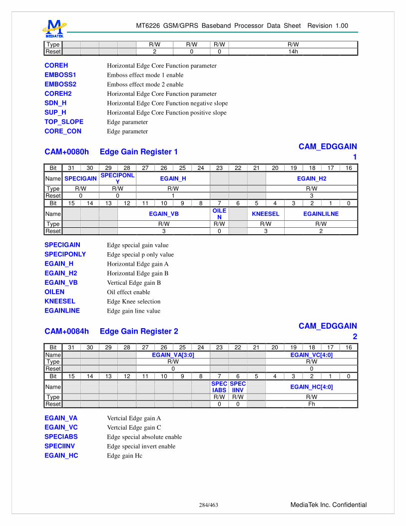
MT6226 GSM/GPRS Baseband Processor Data Sheet Revision 1.00
284/463 MediaTek Inc. Confidential
Type R/W R/W R/W R/W Reset 2 0 0 14h
COREH Horizontal Edge Core Function parameter EMBOSS1 Emboss effect mode 1 enable EMBOSS2 Emboss effect mode 2 enable COREH2 Horizontal Edge Core Function parameter SDN_H Horizontal Edge Core Function negative slope SUP_H Horizontal Edge Core Function positive slope TOP_SLOPE Edge parameter CORE_CON Edge parameter
CAM+0080h Edge Gain Register 1 CAM_EDGGAIN
1 Bit 31 30 29 28 27 26 25 24 23 22 21 20 19 18 17 16
Name SPECIGAIN SPECIPONLY EGAIN_H EGAIN_H2
Type R/W R/W R/W R/W Reset 0 0 1 3
Bit 15 14 13 12 11 10 9 8 7 6 5 4 3 2 1 0
Name EGAIN_VB OILEN KNEESEL EGAINLILNE
Type R/W R/W R/W R/W Reset 3 0 3 2
SPECIGAIN Edge special gain value SPECIPONLY Edge special p only value EGAIN_H Horizontal Edge gain A EGAIN_H2 Horizontal Edge gain B EGAIN_VB Vertical Edge gain B OILEN Oil effect enable KNEESEL Edge Knee selection EGAINLINE Edge gain line value
CAM+0084h Edge Gain Register 2 CAM_EDGGAIN
2 Bit 31 30 29 28 27 26 25 24 23 22 21 20 19 18 17 16
Name EGAIN_VA[3:0] EGAIN_VC[4:0] Type R/W R/W Reset 0 0
Bit 15 14 13 12 11 10 9 8 7 6 5 4 3 2 1 0
Name SPECIABS
SPECIINV EGAIN_HC[4:0]
Type R/W R/W R/W Reset 0 0 Fh
EGAIN_VA Vertcial Edge gain A EGAIN_VC Vertcial Edge gain C SPECIABS Edge special absolute enable SPECIINV Edge special invert enable EGAIN_HC Edge gain Hc

MT6226 GSM/GPRS Baseband Processor Data Sheet Revision 1.00
285/463 MediaTek Inc. Confidential
CAM+0088h Edge Threshold Register CAM_EDGTHR
E Bit 31 30 29 28 27 26 25 24 23 22 21 20 19 18 17 16
Name ETH3 ETH_CON Type R/W R/W Reset 32h 80h
Bit 15 14 13 12 11 10 9 8 7 6 5 4 3 2 1 0
Name ONLYC THRE_EDGE_SUP THRL_EDGE_SUP
Type R/W R/W R/W Reset 0 07h 07h
ETH3 Edge parameter ETH_CON Edge parameter ONLYC Edge enhanced C component only enable THRE_EDGE_SUP Edge parameter THRL_EDGE_SUP Edge parameter
CAM+008Ch Edge Vertical Control Register CAM_EDGVCO
N Bit 31 30 29 28 27 26 25 24 23 22 21 20 19 18 17 16
Name HPEN E_TH1_V HALF_V Type R/W R/W R/W Reset 0 18h 1Fh
Bit 15 14 13 12 11 10 9 8 7 6 5 4 3 2 1 0 Name VPEN SUP_V SDN_V E_TH3_V Type R/W R/W R/W R/W Reset 0 0 2 32h
HPEN Horizontal Edge high pass enable E_TH1_V Edge parameter HALF_V Edge parameter VPEN Vertcial Edge high pass enable SUP_V Vertical Edge Core Function negative slope SDN_V Vertical Edge Core Function negative slope E_TH3_V Edge parameter
CAM+0090h Axis RGB Gain Register CAM_AXGAIN Bit 31 30 29 28 27 26 25 24 23 22 21 20 19 18 17 16
Name R_GAIN Type R/W Reset 3Fh
Bit 15 14 13 12 11 10 9 8 7 6 5 4 3 2 1 0 Name G_GAIN B_GAIN Type R/W R/W Reset 3Fh 3Fh
R_GAIN Axis R component gain G_GAIN Axis G component gain B_GAIN Axis B component gain
CAM+0094h AWB Configuration Register CAM_OPDCFG Bit 31 30 29 28 27 26 25 24 23 22 21 20 19 18 17 16

MT6226 GSM/GPRS Baseband Processor Data Sheet Revision 1.00
286/463 MediaTek Inc. Confidential
Name OPDEN
OPDCLR SUPSEL U_GAIN
Type R/W R/W R/W R/W Reset 1 0 3 1Fh
Bit 15 14 13 12 11 10 9 8 7 6 5 4 3 2 1 0 Name V_GAIN Y_LIMIT Type R/W R/W Reset 1Fh 3
OPDEN AWB counter enable OPDCLR AWB counter clear enable SUPSEL AWB white point RGB upper boundary, which is 192 + 8*SUPSEL U_GAIN AWB U gain value V_GAIN AWB V gain value Y_LIMIT AWB white point luminance limit
CAM+0098h AWB Component Parameter Register CAM_OPDPAR Bit 31 30 29 28 27 26 25 24 23 22 21 20 19 18 17 16
Name S_RB_P S_RB_N Type R/W R/W Reset 7Fh 7Fh
Bit 15 14 13 12 11 10 9 8 7 6 5 4 3 2 1 0 Name S_MG_P S_MG_N Type R/W R/W Reset 7Fh 7Fh
S_RB_P AWB SR Bp value S_RB_N AWB SR Bn value S_MG_P AWB SMGp value S_MG_N AWB SNGn value
CAM+009Ch Color Matrix 1 Register CAM_MATRIX1 Bit 31 30 29 28 27 26 25 24 23 22 21 20 19 18 17 16
Name M11 Type R/W Reset 20h
Bit 15 14 13 12 11 10 9 8 7 6 5 4 3 2 1 0 Name M12 M13 Type R/W R/W Reset 80h 80h
M11 Color matrix 11 value M12 Color matrix 12 value M13 Color matrix 13 value
CAM+00A0h Color Matrix 2 Register CAM_MATRIX2 Bit 31 30 29 28 27 26 25 24 23 22 21 20 19 18 17 16
Name M21 Type R/W Reset 80h
Bit 15 14 13 12 11 10 9 8 7 6 5 4 3 2 1 0 Name M22 M23 Type R/W R/W Reset 20h 80h
M21 Color matrix 21 value M22 Color matrix 22 value

MT6226 GSM/GPRS Baseband Processor Data Sheet Revision 1.00
287/463 MediaTek Inc. Confidential
M23 Color matrix 23 value
CAM+00A4h Color Matrix 3 Register CAM_MATRIX3 Bit 31 30 29 28 27 26 25 24 23 22 21 20 19 18 17 16
Name M31 Type R/W Reset 80h
Bit 15 14 13 12 11 10 9 8 7 6 5 4 3 2 1 0 Name M32 M33 Type R/W R/W Reset 80h 20h
M31 Color matrix 31 value M32 Color matrix 32 value M33 Color matrix 33 value
CAM+00A8h Color Matrix RGB Gain Register CAM_MTXGAIN Bit 31 30 29 28 27 26 25 24 23 22 21 20 19 18 17 16
Name R_GAIN Type R/W Reset 20h
Bit 15 14 13 12 11 10 9 8 7 6 5 4 3 2 1 0 Name G_GAIN B_GAIN Type R/W R/W Reset 20h 20h
R_GAIN Color matrix R component gain value G_GAIN Color matrix G component gain value B_GAIN Color matrix B component gain value
CAM+00ACh Color Process Stage Control Register 2 CAM_CPSCON2 Bit 31 30 29 28 27 26 25 24 23 22 21 20 19 18 17 16
Name Type Reset
Bit 15 14 13 12 11 10 9 8 7 6 5 4 3 2 1 0
Name BYPGM
RGBEDGEN
YEDGEN
OPRGM_IVT Y_EGAIN
Type R/W R/W R/W R/W R/W Reset 1 0 0 0 2
BYPGM Bypass gamma enable RGBEDGAINEN Edge enhanced before gamma operation YEDGEN Edge enhanced after gamma operation OPDGM_IVT Gamma output inverse mode enable Y_EGAIN Y channel edge gain value
CAM+00B0h Color RGB Gain Register CAM_CGAIN Bit 31 30 29 28 27 26 25 24 23 22 21 20 19 18 17 16
Name RGAIN Type R/W Reset 80h
Bit 15 14 13 12 11 10 9 8 7 6 5 4 3 2 1 0 Name GGAIN BGAIN Type R/W R/W Reset 80h 80h

MT6226 GSM/GPRS Baseband Processor Data Sheet Revision 1.00
288/463 MediaTek Inc. Confidential
RGAIN Color R gain (1.7) GGAIN Color G gain (1.7) BGAIN Color B gain (1.7)
CAM+00B4h Gamma RGB Flare Register CAM_GAMFLR
E Bit 31 30 29 28 27 26 25 24 23 22 21 20 19 18 17 16
Name SIGN_R FLARE_R
Type R/W R/W Reset 0 0
Bit 15 14 13 12 11 10 9 8 7 6 5 4 3 2 1 0
Name SIGN_G FLAIRE_G SIGN
_B FLARE_B
Type R/W R/W R/W R/W Reset 0 0 0 0
SIGN_R R Flare sign FLARE_R R Flare value SIGN_G G Flare sign FLARE_G G Flare value SIGN_B B Flare sign FLARE_B B Flare value
CAM+00B8h Y Channel Configuration Register CAM_YCHAN Bit 31 30 29 28 27 26 25 24 23 22 21 20 19 18 17 16
Name CONTRAST_GAIN Type R/W Reset 40h
Bit 15 14 13 12 11 10 9 8 7 6 5 4 3 2 1 0
Name
SIGN_BRIGHT_OFFSE
T
BRIGHT_OFFSET VSUP_EN UV_L
P_EN CSUP_EDGE_GAIN
Type R/W R/W R/W R/W R/W Reset 1 0 0 0 10h
CONTRAST_GAIN Y channel contrast gain value SIGN_BRIGHT_OFFSET Sign bit of Y channel brightness offset value BRIGHT_OFFSET Y channel brightness offset value VSUP_EN Vertical Edge color suppression enable UV_LP_EN UV channel low pass enable CSUP_EDGE_GAIN Chroma suppression edge gain value(1.3)
CAM+00BCh UV Channel Configuration Register CAM_UVCHAN Bit 31 30 29 28 27 26 25 24 23 22 21 20 19 18 17 16
Name U11 V22 Type R/W R/W Reset 20h 20h
Bit 15 14 13 12 11 10 9 8 7 6 5 4 3 2 1 0
Name SIGN_U_OFFSET
U_OFFSET SIGN_V_OFFSET
V_OFFSET
Type R/W R/W R/W R/W Reset 0 0 0 0

MT6226 GSM/GPRS Baseband Processor Data Sheet Revision 1.00
289/463 MediaTek Inc. Confidential
U11 Hue U channel operating value V11 Hue V channel operating value SIGN_U_OFFSET Sign bit of Hue U channel offset value U_OFFSET Hue U channel offset value SIGN_V_OFFSET Sign bit of Hue V channel offset value V_OFFSET Hue V channel offset value
CAM+00C0h Space Convert YUV Register 1 CAM_SCONV1 Bit 31 30 29 28 27 26 25 24 23 22 21 20 19 18 17 16
Name Y_GAIN Type R/W Reset FFh
Bit 15 14 13 12 11 10 9 8 7 6 5 4 3 2 1 0 Name U_GAIN V_GAIN Type R/W R/W Reset 91h B8h
Y_GAIN Space Convert Y channel gain value U_GAIN Space Convert U channel gain value V_GAIN Space Convert V channel gain value
CAM+00C4h Space Convert YUV Register 2 CAM_SCONV2 Bit 31 30 29 28 27 26 25 24 23 22 21 20 19 18 17 16
Name Y_OFFSET Type R/W Reset 01h
Bit 15 14 13 12 11 10 9 8 7 6 5 4 3 2 1 0 Name U_OFFSET V_OFFSET Type R/W R/W Reset 80h 80h
Y_OFFSET Space Convert Y channel offset value U_OFFSET Space Convert U channel offset value V_OFFSET Space Convert V channel offset value
CAM+00C8h Gamma Operation Register 1 CAM_GAMMA1 Bit 31 30 29 28 27 26 25 24 23 22 21 20 19 18 17 16
Name GAMMA_B1 GAMMA_B2 Type R/W R/W Reset 32h 50h
Bit 15 14 13 12 11 10 9 8 7 6 5 4 3 2 1 0 Name GAMMA_B3 GAMMA_B4 Type R/W R/W Reset 65h 76h
GAMMA_B1 Gamma operating B1 value GAMMA_B2 Gamma operating B2 value GAMMA_B3 Gamma operating B3 value GAMMA_B4 Gamma operating B4 value
CAM+00CCh Gamma Operation Register 2 CAM_GAMMA2 Bit 31 30 29 28 27 26 25 24 23 22 21 20 19 18 17 16
Name GAMMA_B5 GAMMA_B6 Type R/W R/W Reset 94h Aeh
Bit 15 14 13 12 11 10 9 8 7 6 5 4 3 2 1 0

MT6226 GSM/GPRS Baseband Processor Data Sheet Revision 1.00
290/463 MediaTek Inc. Confidential
Name GAMMA_B7 GAMMA_B8 Type R/W R/W Reset C5h Dah
GAMMA_B5 Gamma operating B5 value GAMMA_B6 Gamma operating B6 value GAMMA_B7 Gamma operating B7 value GAMMA_B8 Gamma operating B8 value
CAM+00D0h Gamma Operation Register 3 CAM_GAMMA3 Bit 31 30 29 28 27 26 25 24 23 22 21 20 19 18 17 16
Name GAMMA_B9 GAMMA_B10 Type R/W R/W Reset E4h EDh
Bit 15 14 13 12 11 10 9 8 7 6 5 4 3 2 1 0
Name GAMMA_B11
GAMMA_TABLE_SEL
Type R/W R/W Reset F7h 0
GAMMA_B9 Gamma operating B9 value GAMMA_B10 Gamma operating B10 value GAMMA_B11 Gamma operating B11 value GAMMA_TABLE_SEL Gamma table select
0 piecewise-linear approximation 1 10-bit to 8-bit Gamma table
CAM+00D4h AWB Y Result Register CAM_OPDY Bit 31 30 29 28 27 26 25 24 23 22 21 20 19 18 17 16
Name OPD_Y[31:16] Type RO Reset 0
Bit 15 14 13 12 11 10 9 8 7 6 5 4 3 2 1 0 Name OPD_Y[15:0] Type RO Reset 0
OPD_Y AWB Y component accumulation result
CAM+00D8h AWB MG Result Register CAM_OPDMG Bit 31 30 29 28 27 26 25 24 23 22 21 20 19 18 17 16
Name OPD_MG[31:16] Type RO Reset 0
Bit 15 14 13 12 11 10 9 8 7 6 5 4 3 2 1 0 Name OPD_MG[15:0] Type RO Reset 0
OPD_MG AWB MG component accumulation result
CAM+00DCh AWB RB Result Register CAM_OPDRB Bit 31 30 29 28 27 26 25 24 23 22 21 20 19 18 17 16
Name OPD_RB[31:16] Type RO

MT6226 GSM/GPRS Baseband Processor Data Sheet Revision 1.00
291/463 MediaTek Inc. Confidential
Reset 0 Bit 15 14 13 12 11 10 9 8 7 6 5 4 3 2 1 0
Name OPD_RB[15:0] Type RO Reset 0
OPD_RB AWB RB component accumulation result
CAM+00E0h AWB Pixel Count Register CAM_OPDCNT Bit 31 30 29 28 27 26 25 24 23 22 21 20 19 18 17 16
Name PXLCNT Type R Reset 0
Bit 15 14 13 12 11 10 9 8 7 6 5 4 3 2 1 0 Name PXLCNT Type RO Reset 0
PXLCNT AWB pixel counter accumulation result
CAM+00E4h AE Result 1 Register CAM_AE0RLT Bit 31 30 29 28 27 26 25 24 23 22 21 20 19 18 17 16
Name SUM_AE1[28:16] Type RO Reset 0
Bit 15 14 13 12 11 10 9 8 7 6 5 4 3 2 1 0 Name SUM_AE1[15:0] Type RO Reset 0
SUM_AE1 AE window 1 accumulation result
CAM+00E8h AE Result 2 Register CAM_AE1RLT Bit 31 30 29 28 27 26 25 24 23 22 21 20 19 18 17 16
Name SUM_AE2[28:16] Type RO Reset 0
Bit 15 14 13 12 11 10 9 8 7 6 5 4 3 2 1 0 Name SUM_AE2[15:0] Type RO Reset 0
SUM_AE2 AE window 2 accumulation result
CAM+00ECh AE Result 3 Register CAM_AE2RLT Bit 31 30 29 28 27 26 25 24 23 22 21 20 19 18 17 16
Name SUM_AE3[28:16] Type RO Reset 0
Bit 15 14 13 12 11 10 9 8 7 6 5 4 3 2 1 0 Name SUM_AE3[15:0] Type RO Reset 0

MT6226 GSM/GPRS Baseband Processor Data Sheet Revision 1.00
292/463 MediaTek Inc. Confidential
SUM_AE3 AE window 3 accumulation result
CAM+00F0h AE Result 4 Register CAM_AE3RLT Bit 31 30 29 28 27 26 25 24 23 22 21 20 19 18 17 16
Name SUM_AE4[28:16] Type RO Reset 0
Bit 15 14 13 12 11 10 9 8 7 6 5 4 3 2 1 0 Name SUM_AE4[15:0] Type RO Reset 0
SUM_AE4 AE window 4 accumulation result
CAM+00F4h AE Result 5 Register CAM_AE4RLT Bit 31 30 29 28 27 26 25 24 23 22 21 20 19 18 17 16
Name SUM_AE5[28:16] Type RO Reset 0
Bit 15 14 13 12 11 10 9 8 7 6 5 4 3 2 1 0 Name SUM_AE5[15:0] Type RO Reset 0
SUM_AE5 AE window 5 accumulation result
CAM+00F8h AE Result 6 Register CAM_ AE5RLT Bit 31 30 29 28 27 26 25 24 23 22 21 20 19 18 17 16
Name SUM_AE6[28:16] Type RO Reset 0
Bit 15 14 13 12 11 10 9 8 7 6 5 4 3 2 1 0 Name SUM_AE6[15:0] Type RO Reset 0
SUM_AE6 AE window 6 accumulation result
CAM+00FCh AE Result 7 Register CAM_ AE6RLT Bit 31 30 29 28 27 26 25 24 23 22 21 20 19 18 17 16
Name SUM_AE7[28:16] Type RO Reset 0
Bit 15 14 13 12 11 10 9 8 7 6 5 4 3 2 1 0 Name SUM_AE7[15:0] Type RO Reset 0
SUM_AE7 AE window 7 accumulation result
CAM+0100h AE Result 8 Register CAM_ AE7RLT Bit 31 30 29 28 27 26 25 24 23 22 21 20 19 18 17 16
Name SUM_AE8[28:16]

MT6226 GSM/GPRS Baseband Processor Data Sheet Revision 1.00
293/463 MediaTek Inc. Confidential
Type RO Reset 0
Bit 15 14 13 12 11 10 9 8 7 6 5 4 3 2 1 0 Name SUM_AE8[15:0] Type RO Reset 0
SUM_AE8 AE window 8 accumulation result
CAM+0104h AE Result 9 Register CAM_ AE8RLT Bit 31 30 29 28 27 26 25 24 23 22 21 20 19 18 17 16
Name SUM_AE9[28:16] Type RO Reset 0
Bit 15 14 13 12 11 10 9 8 7 6 5 4 3 2 1 0 Name SUM_AE9[15:0] Type RO Reset 0
SUM_AE9 AE window 9 accumulation result
CAM+0108h CAM Histogram Result 1 CAM_HISRLT0 Bit 31 30 29 28 27 26 25 24 23 22 21 20 19 18 17 16
Name CAM_HISRLT1[21:16] Type RO Reset 0
Bit 15 14 13 12 11 10 9 8 7 6 5 4 3 2 1 0 Name CAM_HISRLT1[15:0] Type RO Reset 0
CAM_HISRLT1 Histogram level 1 count result
CAM+010Ch CAM Histogram Result 2 CAM_HISRLT1 Bit 31 30 29 28 27 26 25 24 23 22 21 20 19 18 17 16
Name CAM_HISRLT2[21:16] Type RO Reset 0
Bit 15 14 13 12 11 10 9 8 7 6 5 4 3 2 1 0 Name CAM_HISRLT2[15:0] Type RO Reset 0
CAM_HISRLT2 Histogram level 2 count result
CAM+0110h CAM Histogram Result 3 CAM_HISRLT2 Bit 31 30 29 28 27 26 25 24 23 22 21 20 19 18 17 16
Name CAM_HISRLT3[21:16] Type RO Reset 0
Bit 15 14 13 12 11 10 9 8 7 6 5 4 3 2 1 0 Name CAM_HISRLT3[15:0] Type RO Reset 0

MT6226 GSM/GPRS Baseband Processor Data Sheet Revision 1.00
294/463 MediaTek Inc. Confidential
CAM_HISRLT3 Histogram level 3 count result
CAM+0114h CAM Histogram Result 4 CAM_HISRLT3 Bit 31 30 29 28 27 26 25 24 23 22 21 20 19 18 17 16
Name CAM_HISRLT4[21:16] Type RO Reset 0
Bit 15 14 13 12 11 10 9 8 7 6 5 4 3 2 1 0 Name CAM_HISRLT4[15:0] Type RO Reset 0
CAM_HISRLT4 Histogram level 4 count result
CAM+0118h CAM Histogram Result 5 CAM_HISRLT4 Bit 31 30 29 28 27 26 25 24 23 22 21 20 19 18 17 16
Name CAM_HISRLT5[21:16] Type RO Reset 0
Bit 15 14 13 12 11 10 9 8 7 6 5 4 3 2 1 0 Name CAM_HISRLT5[15:0] Type RO Reset 0
CAM_HISRLT5 Histogram level 5 count result
CAM+011Ch Low Pass Filter Control Register CAM_LPFCON Bit 31 30 29 28 27 26 25 24 23 22 21 20 19 18 17 16
Name YCBCRIN_FAST
Type R/W Reset 0
Bit 15 14 13 12 11 10 9 8 7 6 5 4 3 2 1 0
Name Y_LPFEN C_LP
FEN
Type R/W R/W Reset 0 1
YCBCRIN_FAST YCbCr422 input fast mode Y_LPFEN Enable Luminance channel low pass filter, if V_LPF_EN is off, only do horizontal low pass C_LPFEN Enable Chrominance channel low pass filter, if V_LPF_EN is off, only do horizontal low pass
CAM+0120h Y Low Pass Filter Control Register CAM_LPFY Bit 31 30 29 28 27 26 25 24 23 22 21 20 19 18 17 16
Name LPFY_WEIGHT0[7:0] LPFY_WEIGHT1[7:0] Type R/W R/W Reset 0 0
Bit 15 14 13 12 11 10 9 8 7 6 5 4 3 2 1 0 Name LPFY_WEIGHT2[7:0] LPFY_WEIGHT3[7:0] Type R/W R/W Reset 0 0

MT6226 GSM/GPRS Baseband Processor Data Sheet Revision 1.00
295/463 MediaTek Inc. Confidential
LPFY_WEIGHT0 Y low pass filter weighting 0 LPFY_WEIGHT1 Y low pass filter weighting 1 LPFY_WEIGHT2 Y low pass filter weighting 2 LPFY_WEIGHT3 Y low pass filter weighting 3
CAM+0124h CbCr Low Pass Filter Control Register CAM_LPFC Bit 31 30 29 28 27 26 25 24 23 22 21 20 19 18 17 16
Name LPFC_WEIGHT0[7:0] LPFC_WEIGHT1[7:0] Type R/W R/W Reset 0 0
Bit 15 14 13 12 11 10 9 8 7 6 5 4 3 2 1 0 Name LPFC_WEIGHT2[7:0] LPFC_WEIGHT[7:0] Type R/W R/W Reset 0 0
LPFC_WEIGHT0 CbCr low pass filter weighting 0 LPFC _WEIGHT1 CbCr low pass filter weighting 1 LPFC _WEIGHT2 CbCr low pass filter weighting 2 LPFC _WEIGHT3 CbCr low pass filter weighting 3
CAM+0128h Vertical Subsample Control Register CAM_VSUB Bit 31 30 29 28 27 26 25 24 23 22 21 20 19 18 17 16
Name V_SUB_EN V_SUB_IN
Type R/W R/W Reset 0 0
Bit 15 14 13 12 11 10 9 8 7 6 5 4 3 2 1 0 Name V_SUB_OUT Type R/W Reset 0
V_SUB_EN Vertical sub-sample enable V_SUB_IN Source vertical size V_SUB_OUT Sub-sample vertical size
CAM+012ch Horizontal Subsample Control Register CAM_HSUB Bit 31 30 29 28 27 26 25 24 23 22 21 20 19 18 17 16
Name H_SUB_EN H_SUB_IN
Type R/W R/W Reset 0 0
Bit 15 14 13 12 11 10 9 8 7 6 5 4 3 2 1 0 Name H_SUB_OUT Type R/W Reset 0
H_SUB_EN Horizontal sub-sample enable H_SUB_IN Source horizontal size H_SUB_OUT Sub-sample horizontal size

MT6226 GSM/GPRS Baseband Processor Data Sheet Revision 1.00
296/463 MediaTek Inc. Confidential
CAM+0130h Sensor Gamma R0 Register CAM_SGAMMA
R0 Bit 31 30 29 28 27 26 25 24 23 22 21 20 19 18 17 16
Name SGAMMA_E
N
SGAMMA_IVT
R_B1
Type R/W R/W R/W Reset 0 0 32h
Bit 15 14 13 12 11 10 9 8 7 6 5 4 3 2 1 0 Name R_B2 R_B3 Type R/W R/W Reset 50h 65h
SGAMMA_EN Sensor Gamma enable SGAMMA_IVT Sensor Gamma output invert R_B1 Gamma operating B1 value R_B2 Gamma operating B2 value R_B3 Gamma operating B3 value
CAM+0134h Sensor Gamma R1 Register CAM_SGAMMA
R1 Bit 31 30 29 28 27 26 25 24 23 22 21 20 19 18 17 16
Name R_B4 R_B5 Type R/W R/W Reset 76h 94h
Bit 15 14 13 12 11 10 9 8 7 6 5 4 3 2 1 0 Name R_B6 R_B7 Type R/W R/W Reset AEh C5h
R_B4 Gamma operating B4 value R_B5 Gamma operating B5 value R_B6 Gamma operating B6 value R_B7 Gamma operating B7 value
CAM+0138h Sensor Gamma R2 Register CAM_SGAMMA
R2 Bit 31 30 29 28 27 26 25 24 23 22 21 20 19 18 17 16
Name R_B8 R_B9 Type R/W R/W Reset DAh D4h
Bit 15 14 13 12 11 10 9 8 7 6 5 4 3 2 1 0 Name R_B10 R_B11 Type R/W R/W Reset EDh F7h
R_B8 Gamma operating B8 value R_B9 Gamma operating B9 value R_B10 Gamma operating B10 value R_B11 Gamma operating B11 value
CAM+013ch Sensor Gamma GR0 Register CAM_SGAMMA
GR0 Bit 31 30 29 28 27 26 25 24 23 22 21 20 19 18 17 16

MT6226 GSM/GPRS Baseband Processor Data Sheet Revision 1.00
297/463 MediaTek Inc. Confidential
Name GR_B1 GR_B2 Type R/W R/W Reset 32h 50h
Bit 15 14 13 12 11 10 9 8 7 6 5 4 3 2 1 0 Name GR_B3 GR_B4 Type R/W R/W Reset 65h 76h
GR_B1 Gamma operating B1 value GR_B2 Gamma operating B2 value GR_B3 Gamma operating B3 value GR_B4 Gamma operating B4 value
CAM+0140h Sensor Gamma GR1 Register CAM_SGAMMA
GR1 Bit 31 30 29 28 27 26 25 24 23 22 21 20 19 18 17 16
Name GR_B5 GR_B6 Type R/W R/W Reset 94h AEh
Bit 15 14 13 12 11 10 9 8 7 6 5 4 3 2 1 0 Name GR_B7 GR_B8 Type R/W R/W Reset C5h DAh
GR_B5 Gamma operating B5 value GR_B6 Gamma operating B6 value GR_B7 Gamma operating B7 value GR_B8 Gamma operating B8 value
CAM+0144h Sensor Gamma GR2 Register CAM_SGAMMA
GR2 Bit 31 30 29 28 27 26 25 24 23 22 21 20 19 18 17 16
Name GR_B9 GR_B10 Type R/W R/W Reset E4h EDh
Bit 15 14 13 12 11 10 9 8 7 6 5 4 3 2 1 0 Name GR_B11 Type R/W Reset F7h
GR_B9 Gamma operating B9 value GR_B10 Gamma operating B10 value GR_B11 Gamma operating B11 value
CAM+0148h Sensor Gamma B0 Register CAM_SGAMMA
B0 Bit 31 30 29 28 27 26 25 24 23 22 21 20 19 18 17 16
Name B_B1 B_B2 Type R/W R/W Reset 32h 50h
Bit 15 14 13 12 11 10 9 8 7 6 5 4 3 2 1 0 Name B_B3 B_B4 Type R/W R/W Reset 65h 76h
B_B1 Gamma operating B1 value

MT6226 GSM/GPRS Baseband Processor Data Sheet Revision 1.00
298/463 MediaTek Inc. Confidential
B_B2 Gamma operating B2 value B_B3 Gamma operating B3 value B_B4 Gamma operating B4 value
CAM+014ch Sensor Gamma B1 Register CAM_SGAMMA
B1 Bit 31 30 29 28 27 26 25 24 23 22 21 20 19 18 17 16
Name B_B5 B_B6 Type R/W R/W Reset 94h AEh
Bit 15 14 13 12 11 10 9 8 7 6 5 4 3 2 1 0 Name B_B7 B_B8 Type R/W R/W Reset C5h DAh
B_B5 Gamma operating B5 value B_B6 Gamma operating B6 value B_B7 Gamma operating B7 value B_B8 Gamma operating B8 value
CAM+0150h Sensor Gamma B2 Register CAM_SGAMMA
B2 Bit 31 30 29 28 27 26 25 24 23 22 21 20 19 18 17 16
Name B_B9 B_B10 Type R/W R/W Reset E4h EDh
Bit 15 14 13 12 11 10 9 8 7 6 5 4 3 2 1 0 Name B_B11 Type R/W Reset F7h
B_B9 Gamma operating B9 value B_B10 Gamma operating B10 value B_B11 Gamma operating B11 value
CAM+00154h Defect Pixel Configuration Register CAM_DEFECT0 Bit 31 30 29 28 27 26 25 24 23 22 21 20 19 18 17 16
Name DEFECT_E
N
Type R/W Reset 0
Bit 15 14 13 12 11 10 9 8 7 6 5 4 3 2 1 0 Name Type Reset
DEFECT_EN Defect table correct enable
CAM+0158h Defect Pixel Table Address Register CAM_DEFECT1 Bit 31 30 29 28 27 26 25 24 23 22 21 20 19 18 17 16
Name DEFFECT_ADDR[31:16] Type RW Reset 2000h
Bit 15 14 13 12 11 10 9 8 7 6 5 4 3 2 1 0 Name DEFECT_ADDR[15:0]

MT6226 GSM/GPRS Baseband Processor Data Sheet Revision 1.00
299/463 MediaTek Inc. Confidential
Type RW Reset 0
DEFECT_ADDR Defect table location address
CAM+0160h Sensor Gamma GB0 Register CAM_SGAMMA
GB0 Bit 31 30 29 28 27 26 25 24 23 22 21 20 19 18 17 16
Name GB_B1 GB_B2 Type R/W R/W Reset 32h 50h
Bit 15 14 13 12 11 10 9 8 7 6 5 4 3 2 1 0 Name GB_B3 GB_B4 Type R/W R/W Reset 65h 76h
GB_B1 Gamma operating B1 value GB_B2 Gamma operating B2 value GB_B3 Gamma operating B3 value GB_B4 Gamma operating B4 value
CAM+0164h Sensor Gamma GB1 Register CAM_SGAMMA
GB1 Bit 31 30 29 28 27 26 25 24 23 22 21 20 19 18 17 16
Name GB_B5 GB_B6 Type R/W R/W Reset 94h AEh
Bit 15 14 13 12 11 10 9 8 7 6 5 4 3 2 1 0 Name GB_B7 GB_B8 Type R/W R/W Reset C5h DAh
GB_B5 Gamma operating B5 value GB_B6 Gamma operating B6 value GB_B7 Gamma operating B7 value GB_B8 Gamma operating B8 value
CAM+0168h Sensor Gamma GB2 Register CAM_SGAMMA
GB2 Bit 31 30 29 28 27 26 25 24 23 22 21 20 19 18 17 16
Name GB_B9 GB_B10 Type R/W R/W Reset E4h EDh
Bit 15 14 13 12 11 10 9 8 7 6 5 4 3 2 1 0 Name GB_B11 Type R/W Reset F7h
GB_B9 Gamma operating B9 value GB_B10 Gamma operating B10 value GB_B11 Gamma operating B11 value

MT6226 GSM/GPRS Baseband Processor Data Sheet Revision 1.00
300/463 MediaTek Inc. Confidential
CAM+016Ch RAW Gain Control Register 1 CAM_RAWGAI
N0 Bit 31 30 29 28 27 26 25 24 23 22 21 20 19 18 17 16
Name RAW_RGAIN Type R/W Reset 80h
Bit 15 14 13 12 11 10 9 8 7 6 5 4 3 2 1 0 Name RAW_GRGAIN Type R/W Reset 80h
RAW_RGAIN Raw R Gain, 0 equal unity gain RAW_GRGAIN Raw GR Gain, 0 equal unity gain
CAM+0170h RAW Gain Control Register 2 CAM_RAWGAI
N1 Bit 31 30 29 28 27 26 25 24 23 22 21 20 19 18 17 16
Name RAW_BGAIN Type R/W Reset 80h
Bit 15 14 13 12 11 10 9 8 7 6 5 4 3 2 1 0 Name RAW_GBGAIN Type R/W Reset 80h
RAW_BGAIN Raw B Gain, 0 equal unity gain RAW_GBGAIN Raw GB Gain, 0 equal unity gain
CAM+0174h Result Window Vertical Size Register RWINV_SEL Bit 31 30 29 28 27 26 25 24 23 22 21 20 19 18 17 16
Name RWIN_EN RWINV_START
Type R/W R/W Reset 0h 0h
Bit 15 14 13 12 11 10 9 8 7 6 5 4 3 2 1 0 Name RWINV_END Type R/W Reset 0h
RWIN_EN Result window enable RWINV_START Result window vertical start line RWINV_END Result window vertical end line
CAM+0178h Result Window Horizontal Size Register RWINH_SEL Bit 31 30 29 28 27 26 25 24 23 22 21 20 19 18 17 16
Name RWINH_START Type R/W Reset 0h
Bit 15 14 13 12 11 10 9 8 7 6 5 4 3 2 1 0 Name RWINH_END Type R/W Reset 0h

MT6226 GSM/GPRS Baseband Processor Data Sheet Revision 1.00
301/463 MediaTek Inc. Confidential
RWINH_START Result window horizontal start pixel RWINH_END Result window horizontal end pixel
CAM+0180h Camera Interface Debug Mode Control Register CAM_DEBUG Bit 31 30 29 28 27 26 25 24 23 22 21 20 19 18 17 16
Name Type Reset
Bit 15 14 13 12 11 10 9 8 7 6 5 4 3 2 1 0 Name Type Reset
CAM+0184h Camera Module Debug Information Write Out Destination Address
CAM_DSTADDR
Bit 31 30 29 28 27 26 25 24 23 22 21 20 19 18 17 16 Name DST_ADD[31:16] Type R/W Reset 4000h
Bit 15 14 13 12 11 10 9 8 7 6 5 4 3 2 1 0 Name DST_ADD[15:0] Type R/W Reset 0000h
DST_ADD Debug Information Write Output Destination Address
CAM+0188h Camera Module Debug Information Last Transfer Destination Address
CAM_LASTADDR
Bit 31 30 29 28 27 26 25 24 23 22 21 20 19 18 17 16 Name LAST_ADD[31:16] Type R/W Reset 0
Bit 15 14 13 12 11 10 9 8 7 6 5 4 3 2 1 0 Name LAST_ADD[15:0] Type R/W Reset 0
LAST_ADD Debug Information Last Transfer Destination Address
CAM+018Ch Camera Module Frame Buffer Transfer Out Count Register
CAM_XFERCNT
Bit 31 30 29 28 27 26 25 24 23 22 21 20 19 18 17 16 Name XFER_COUNT [31:16] Type RO Reset 0
Bit 15 14 13 12 11 10 9 8 7 6 5 4 3 2 1 0 Name XFER_COUNT[15:0] Type RO Reset 0
XFER_COUNT Pixel Transfer Count per Frame

MT6226 GSM/GPRS Baseband Processor Data Sheet Revision 1.00
302/463 MediaTek Inc. Confidential
CAM+0190h Sensor Test Model Configuration Register 1 CAM_MDLCFG
1 Bit 31 30 29 28 27 26 25 24 23 22 21 20 19 18 17 16
Name VSYNC IDLE_PIXEL_PER_LINE Type R/W R/W Reset 0 0
Bit 15 14 13 12 11 10 9 8 7 6 5 4 3 2 1 0
Name LINECHG_E
N
FULL_RAN
GE ON RST STILL PATT
ERN PIXEL_SEL CLK_DIV
Type R/W R/W R/W R/W R/W R/W R/W R/W Reset 0 0 0 0 0 0 0 0
VSYNC VSYNC high duration in line unit(IDLE_PIXEL_PER_LINE + PIXEL) IDLE_PIXEL_PER_LINE HSYNC low duration in pixel unit LINECHG_EN Pattern 0 2 lines change mode enable FULL_RANGE Sensor Model Full Range Enable. When full range is enable, pattern data value will increase progressively every line output. ON Enable Sensor Model. RST Reset Sensor Model STILL Still picture Mode PATTERN Sensor Model Test Pattern Selection PIXEL_SEL Sensor Model output pixel selection.
00 All pixels 01 01 pixel
10 10 pixel 11 00 and 11 pixels
CLK_DIV Pixel_Clock/System_Clock Ratio
CAM +0194h Sensor Test Model Configuration Register 2 CAM_MDLCFG
2 Bit 31 30 29 28 27 26 25 24 23 22 21 20 19 18 17 16
Name LINE Type R/W Reset 0
Bit 15 14 13 12 11 10 9 8 7 6 5 4 3 2 1 0 Name PIXEL Type R/W Reset 0
LINE Sensor Model Line Number PIXEL Sensor Model Pixel Number (HSYNC high duration in pixel unit)
CAM+01CCh AutoDefect Control 1 Register CAM_ADEFEC
T0 Bit 31 30 29 28 27 26 25 24 23 22 21 20 19 18 17 16
Name ADC_EN
ADL_EN
ADR_EN
ADU_EN
ADD_EN
DEADCHEC
K GCHECKSEL RBCHECKS
EL BRIGHTTHD BLACKTHD
Type R/W R/W R/W R/W R/W R/W R/W R/W R/W R/W Reset 0 0 0 0 0 0 0 0 0 0

MT6226 GSM/GPRS Baseband Processor Data Sheet Revision 1.00
303/463 MediaTek Inc. Confidential
Bit 15 14 13 12 11 10 9 8 7 6 5 4 3 2 1 0 Name AE_INTERVAL Type R/W Reset 0
ADC_En Center Autodefect cell enable ADL_En Left Autodefect cell enable ADR_En Right Autodefect cell enable ADU_En Up Autodefect cell enable ADD_En Down Autodefect cell enable DEADCHECK Dead pixel check enable GCHECKSEl G pixel check method selection
00 near group check only 01 near and far groups check
10 far group check only 11 reserved
RBCHECKSEl RB pixel check method selection 00 near group check only 01 near and far groups check 10 far group check only
11 reserved BRIGHTTHD Black pixel threshold = BRIGHTTHD *4 BLACKTHD Black pixel threshold = BLACKTHD *4 AE_INTERVAL AE frame interval
CAM+01D0h AutoDefect Control 2 Register CAM_ADEFECT
1 Bit 31 30 29 28 27 26 25 24 23 22 21 20 19 18 17 16
Name GCHECKTHD RBCHECKTHD Type R/W R/W Reset 0 0
Bit 15 14 13 12 11 10 9 8 7 6 5 4 3 2 1 0 Name GCORRECTTHD RBCORRECTTHD Type R/W R/W Reset 0 0
GCHECKTHD G pixel check threshold RBCHECKTHD RB pixel check threshold GCORRECTTHD G pixel correct threshold RBCORRECTTHD RB pixel correct threshold
CAM+01D4h Flash Control Register CAM_FLASH Bit 31 30 29 28 27 26 25 24 23 22 21 20 19 18 17 16
Name FLASH_OU
T FLAS
H_EN
FLASH_STARTP
NT
FLASH_PO
L FLASH_LNUNIT[3:0]
Type R RW RW RW RW Reset 0 0 0 0
Bit 15 14 13 12 11 10 9 8 7 6 5 4 3 2 1 0
Name FLASH_LNUNIT_NO[7:0] FLASH_FRAME_DELA
Y[1:0]

MT6226 GSM/GPRS Baseband Processor Data Sheet Revision 1.00
304/463 MediaTek Inc. Confidential
Type RW RW Reset 0 0
FLASH_OUT Flash out status
FLASH_EN Flash enable
FLASH_STARTPNT Flash start point
0 Start from vsync start
1 Start from expdone
FLASH_POL Flash line polarity
FLASH_LNUNIT Flash line unit, 0~15 lines
FLASH_LNUNIT_NO Flash line unit count
FLASH_FRAME_DELAY Flash frame delay
CAM +01D8h CAM RESET Register CAM_RESET Bit 31 30 29 28 27 26 25 24 23 22 21 20 19 18 17 16
Name TG_STATUS Type R Reset
Bit 15 14 13 12 11 10 9 8 7 6 5 4 3 2 1 0
Name ISP_FRAME_COUNT[7:0] ISP_RESET
Type RW RW Reset 0 0
ISP_FRAME_COUNT ISP frame counter ISP_RESET ISP reset
CAM +01DCh TG STATUS Register TG_STATUS Bit 31 30 29 28 27 26 25 24 23 22 21 20 19 18 17 16
Name SYN_VFON LINE_COUNT[11:0]
Type R R Reset
Bit 15 14 13 12 11 10 9 8 7 6 5 4 3 2 1 0 Name PIXEL_COUNT[11:0] Type R Reset
SYN_VFON TG view finder status LINE_COUNT TG line counter PIXEL_COUNT TG pixel counter
CAM+01E0h Histogram Boundary Control Register3 CAM_HIS2 Bit 31 30 29 28 27 26 25 24 23 22 21 20 19 18 17 16
Name H6_BND H7_BND Type R/W R/W Reset 60h 70h
Bit 15 14 13 12 11 10 9 8 7 6 5 4 3 2 1 0 Name H8_BND H9_BND Type R/W R/W

MT6226 GSM/GPRS Baseband Processor Data Sheet Revision 1.00
305/463 MediaTek Inc. Confidential
Reset 80h 90H
H6_BND Histogram level 6 up boundary value H7_BND Histogram level 7 up boundary value H8_BND Histogram level 8 up boundary value H9_BND Histogram level 9 up boundary value
CAM+01E4h Histogram Boundary Control Register4 CAM_HIS3 Bit 31 30 29 28 27 26 25 24 23 22 21 20 19 18 17 16
Name HA_BND HB_BND Type R/W R/W Reset a0h b0h
Bit 15 14 13 12 11 10 9 8 7 6 5 4 3 2 1 0 Name HC_BND HD_BND Type R/W R/W Reset c0h d0H
HA_BND Histogram level A up boundary value HB_BND Histogram level B up boundary value HC_BND Histogram level C up boundary value HD_BND Histogram level D up boundary value
CAM+01E8h Histogram Boundary Control Register5 CAM_HIS4 Bit 31 30 29 28 27 26 25 24 23 22 21 20 19 18 17 16
Name HE_BND HF_BND Type R/W R/W Reset e0h f0h
Bit 15 14 13 12 11 10 9 8 7 6 5 4 3 2 1 0 Name AUTODEFECT_NO Type RO Reset
HDE_ND Histogram level E up boundary value HEF_ND Histogram level F up boundary value AUTODEFECT_NO Autodefect corrected pixel count
CAM+01ECh CAM Histogram Result 6 CAM_HISRLT5 Bit 31 30 29 28 27 26 25 24 23 22 21 20 19 18 17 16
Name CAM_HISRLT6[21:16] Type RO Reset 0
Bit 15 14 13 12 11 10 9 8 7 6 5 4 3 2 1 0 Name CAM_HISRLT6[15:0] Type RO Reset 0
CAM_HISRLT6 Histogram level 6 count result
CAM+01F0h CAM Histogram Result 7 CAM_HISRLT6 Bit 31 30 29 28 27 26 25 24 23 22 21 20 19 18 17 16
Name CAM_HISRLT7[21:16] Type RO Reset 0

MT6226 GSM/GPRS Baseband Processor Data Sheet Revision 1.00
306/463 MediaTek Inc. Confidential
Bit 15 14 13 12 11 10 9 8 7 6 5 4 3 2 1 0 Name CAM_HISRLT7[15:0] Type RO Reset 0
CAM_HISRLT7 Histogram level 7 count result
CAM+01F4h CAM Histogram Result 8 CAM_HISRLT7 Bit 31 30 29 28 27 26 25 24 23 22 21 20 19 18 17 16
Name CAM_HISRLT8[21:16] Type RO Reset 0
Bit 15 14 13 12 11 10 9 8 7 6 5 4 3 2 1 0 Name CAM_HISRLT8[15:0] Type RO Reset 0
CAM_HISRLT8 Histogram level 8 count result
CAM+01F8h CAM Histogram Result 9 CAM_HISRLT8 Bit 31 30 29 28 27 26 25 24 23 22 21 20 19 18 17 16
Name CAM_HISRLT9[21:16] Type RO Reset 0
Bit 15 14 13 12 11 10 9 8 7 6 5 4 3 2 1 0 Name CAM_HISRLT9[15:0] Type RO Reset 0
CAM_HISRLT9 Histogram level 9 count result
CAM+01FCh CAM Histogram Result 10 CAM_HISRLT9 Bit 31 30 29 28 27 26 25 24 23 22 21 20 19 18 17 16
Name CAM_HISRLTA[21:16] Type RO Reset 0
Bit 15 14 13 12 11 10 9 8 7 6 5 4 3 2 1 0 Name CAM_HISRLTA[15:0] Type RO Reset 0
CAM_HISRLTA Histogram level A count result
CAM+0200h CAM Histogram Result 11 CAM_HISRLTA Bit 31 30 29 28 27 26 25 24 23 22 21 20 19 18 17 16
Name CAM_HISRLTB[21:16] Type RO Reset 0
Bit 15 14 13 12 11 10 9 8 7 6 5 4 3 2 1 0 Name CAM_HISRLTB[15:0] Type RO Reset 0
CAM_HISRLTB Histogram level B count result

MT6226 GSM/GPRS Baseband Processor Data Sheet Revision 1.00
307/463 MediaTek Inc. Confidential
CAM+0204h CAM Histogram Result 12 CAM_HISRLTB Bit 31 30 29 28 27 26 25 24 23 22 21 20 19 18 17 16
Name CAM_HISRLTC[21:16] Type RO Reset 0
Bit 15 14 13 12 11 10 9 8 7 6 5 4 3 2 1 0 Name CAM_HISRLTC[15:0] Type RO Reset 0
CAM_HISRLTC Histogram level C count result
CAM+0208h CAM Histogram Result 13 CAM_HISRLTC Bit 31 30 29 28 27 26 25 24 23 22 21 20 19 18 17 16
Name CAM_HISRLTD[21:16] Type RO Reset 0
Bit 15 14 13 12 11 10 9 8 7 6 5 4 3 2 1 0 Name CAM_HISRLTD[15:0] Type RO Reset 0
CAM_HISRLTD Histogram level D count result
CAM+020Ch CAM Histogram Result 14 CAM_HISRLTD Bit 31 30 29 28 27 26 25 24 23 22 21 20 19 18 17 16
Name PGAIN_SCOUNT[19:10] CAM_HISRLTE[21:16] Type RO RO Reset 0
Bit 15 14 13 12 11 10 9 8 7 6 5 4 3 2 1 0 Name CAM_HISRLTE[15:0] Type RO Reset 0
PGAIN_SCOUNT Pre-gain saturation count bit 10 to bit19 CAM_HISRLTE Histogram level E count result
CAM+0210h CAM Histogram Result 15 CAM_HISRLTE Bit 31 30 29 28 27 26 25 24 23 22 21 20 19 18 17 16
Name PGAIN_SCOUNT[9:0] CAM_HISRLTF[21:16] Type RO RO Reset 0
Bit 15 14 13 12 11 10 9 8 7 6 5 4 3 2 1 0 Name CAM_HISRLTF[15:0] Type RO Reset 0
PGAIN_SCOUNT Pre-gain saturation count bit 0 to bit9 CAM_HISRLTF Histogram level F count result

MT6226 GSM/GPRS Baseband Processor Data Sheet Revision 1.00
308/463 MediaTek Inc. Confidential
CAM+00214h Shading Cotrol 1 Register CAM_SHADING
1 Bit 31 30 29 28 27 26 25 24 23 22 21 20 19 18 17 16
Name
SHADING_
RANGE[8]
SHADING_
RANGE_EN
SHADING_E
N SHADING_CENTERY[11:0]
Type RW RW RW RW Reset 0 0 0 0
Bit 15 14 13 12 11 10 9 8 7 6 5 4 3 2 1 0
Name K_FACTOR RADIUS_FACTOR SHADING_CENTERX[11:0]
Type R/W R/W RW Reset 0 0 0
SHADING_RANGE[8] Shading range bit 8
SHADING_RANGE_EN Shading range enable
SHADING_EN Shading enable
Shading_out = Shading_in*(1+Compensation_Ratio)
Where Compensation_Ratio = Effective_Range*(K>>(26-K_FACTOR))
K = KR when R pixel, KG when G pixel, KB when B pixel
K_FACTOR Shading parameter factor, used to scale up parameter.
RADIUS_FACTOR Radius factor, select effective radius range.
Effective_Range = ((effective_diffx)^2) + ((effective_diffy)^2)
Where effective_diffx = (x-centerx)>>(3-RADIUS_FACTOR)
effective_diffy = (y-centery)>>(3-RADIUS_FACTOR)
Because of hardware limitation,
effective maximum radius(range between center) is
00 Effective maximum radius : 4095
01 Effective maximum radius : 2047
02 Effective maximum radius : 1023
03 Effective maximum radius : 511
SHADING_CENTERY Shading center y coordinate x 2
SHADING_CENTERX Shading center x coordinate x 2
CAM+0218h Shading Control 2 Register CAM_SHADING
2 Bit 31 30 29 28 27 26 25 24 23 22 21 20 19 18 17 16
Name SHADING_KR[7:0] SHADING_KG[7:0] Type RW RW Reset 0 0

MT6226 GSM/GPRS Baseband Processor Data Sheet Revision 1.00
309/463 MediaTek Inc. Confidential
Bit 15 14 13 12 11 10 9 8 7 6 5 4 3 2 1 0 Name SHADING_KB[7:0] SHADING_RANGE[7:0] Type RW R/W Reset 0 ff
SHADING_KR Shading R pixel parameter
SHADING_KG Shading G pixel parameter
SHADING_KB Shading B pixel parameter
SHADING_RANGE Shading range, bit8 refer to 0x214 bit 30
CAM+021Ch Shading R Curve Register 1 CAM_SRCURV
E0 Bit 31 30 29 28 27 26 25 24 23 22 21 20 19 18 17 16
Name
SHADING_CURVE_EN
SHADING_I
VT
SHADING_CURVE_SEL SHADING_R_B1
Type R/W R/W R/W R/W Reset 0 0 0 20h
Bit 15 14 13 12 11 10 9 8 7 6 5 4 3 2 1 0 Name SHADING_R_B2 SHADING_R_B3 Type R/W R/W Reset 40h 60h
SHADING_CURVE_EN Shading curve enable SHADING_IVT Shading curve output invert SHADING_CURVE_SEL Shading curve input selection
00 1/8 Effective_Range input 01 1/4 Effective_Range input 02 1/2 Effecitve_Range input 03 Effective Range input
RADIUS_FACTOR CURVE_SEL Maximum Curve Boundary VGA (640x480) 3 2 B6 SVGA (800x600) 3 2 B11 XGA (1024x768) 2 1 B8 SXGA (1280x1024) 2 2 B6 UXGA (1600x1200) 2 2 B11
SHADING_R_B1 R shading curve operating B1 value SHADING_R_B2 R shading curve operating B2 value SHADING_R_B3 R shading curve operating B3 value
CAM+0220h Shading R Curve Register 2 CAM_SRCURV
E1 Bit 31 30 29 28 27 26 25 24 23 22 21 20 19 18 17 16
Name SHADING_R_B4 SHADING_R_B5 Type R/W R/W Reset 80h 90h
Bit 15 14 13 12 11 10 9 8 7 6 5 4 3 2 1 0 Name SHADING_R_B6 SHADING_R_B7 Type R/W R/W

MT6226 GSM/GPRS Baseband Processor Data Sheet Revision 1.00
310/463 MediaTek Inc. Confidential
Reset A0h B0h
SHADING_R_B4 R shading curve operating B4 value SHADING_R_B5 R shading curve operating B5 value SHADING_R_B6 R shading curve operating B6 value SHADING_R_B7 R shading curve operating B7 value
CAM+0224h Shading R Curve Register 3 CAM_SRCURV
E2 Bit 31 30 29 28 27 26 25 24 23 22 21 20 19 18 17 16
Name SHADING_R_B8 SHADING_R_B9 Type R/W R/W Reset C0h D0h
Bit 15 14 13 12 11 10 9 8 7 6 5 4 3 2 1 0 Name SHADING_R_B10 SHADING_R_B11 Type R/W R/W Reset E0h F0h
SHADING_R_B8 R shading curve operating B8 value SHADING_R_B9 R shading curve operating B9 value SHADING_R_B10 R shading curve operating B10 value SHADING_R_B11 R shading curve operating B11 value
CAM+0228h Shading G Curve Register 1 CAM_SGCURV
E0 Bit 31 30 29 28 27 26 25 24 23 22 21 20 19 18 17 16
Name SHADING_G_B1 SHADING_G_B2 Type R/W R/W Reset 20h 40h
Bit 15 14 13 12 11 10 9 8 7 6 5 4 3 2 1 0 Name SHADING_G_B3 SHADING_G_B4 Type R/W R/W Reset 60h 80h
SHADING_G_B1 G shading curve operating B1 value SHADING_G_B2 G shading curve operating B2 value SHADING_G_B3 G shading curve operating B3 value SHADING_G_B4 G shading curve operating B4 value
CAM+022Ch Shading G Curve Register 2 CAM_SGCURV
E1 Bit 31 30 29 28 27 26 25 24 23 22 21 20 19 18 17 16
Name SHADING_G_B5 SHADING_G_B6 Type R/W R/W Reset 90h A0h
Bit 15 14 13 12 11 10 9 8 7 6 5 4 3 2 1 0 Name SHADING_G_B7 SHADING_G_B8 Type R/W R/W Reset B0h C0h
SHADING_G_B5 G shading curve operating B5 value SHADING_G_B6 G shading curve operating B6 value

MT6226 GSM/GPRS Baseband Processor Data Sheet Revision 1.00
311/463 MediaTek Inc. Confidential
SHADING_G_B7 G shading curve operating B7 value SHADING_G_B8 G shading curve operating B8 value
CAM+0230h Shading G Curve Register 3 CAM_SGCURV
E2 Bit 31 30 29 28 27 26 25 24 23 22 21 20 19 18 17 16
Name SHADING_G_B9 SHADING_G_B10 Type R/W R/W Reset D0h E0h
Bit 15 14 13 12 11 10 9 8 7 6 5 4 3 2 1 0 Name SHADING_G_B11 Type R/W Reset F0h
SHADING_G_B9 G shading curve operating B9 value SHADING_G_B10 G shading curve operating B10 value SHADING_G_B11 G shading curve operating B11 value
CAM+0234h Shading B Curve Register 1 CAM_SBCURV
E0 Bit 31 30 29 28 27 26 25 24 23 22 21 20 19 18 17 16
Name SHADING_B_B1 SHADING_B_B2 Type R/W R/W Reset 20h 40h
Bit 15 14 13 12 11 10 9 8 7 6 5 4 3 2 1 0 Name SHADING_B_B3 SHADING_B_B4 Type R/W R/W Reset 60h 80h
SHADING_B_B1 B shading curve operating B1 value SHADING_B_B2 B shading curve operating B2 value SHADING_B_B3 B shading curve operating B3 value SHADING_B_B4 B shading curve operating B4 value
CAM+0238h Shading B Curve Register 2 CAM_SGCURV
E1 Bit 31 30 29 28 27 26 25 24 23 22 21 20 19 18 17 16
Name SHADING_B_B5 SHADING_B_B6 Type R/W R/W Reset 90h A0h
Bit 15 14 13 12 11 10 9 8 7 6 5 4 3 2 1 0 Name SHADING_B_B7 SHADING_B_B8 Type R/W R/W Reset B0h C0h
SHADING_B_B5 G shading curve operating B5 value SHADING_B_B6 G shading curve operating B6 value SHADING_B_B7 G shading curve operating B7 value SHADING_B_B8 G shading curve operating B8 value

MT6226 GSM/GPRS Baseband Processor Data Sheet Revision 1.00
312/463 MediaTek Inc. Confidential
CAM+023Ch Shading B Curve Register 3 CAM_SBCURV
E2 Bit 31 30 29 28 27 26 25 24 23 22 21 20 19 18 17 16
Name SHADING_B_B9 SHADING_B_B10 Type R/W R/W Reset D0h E0h
Bit 15 14 13 12 11 10 9 8 7 6 5 4 3 2 1 0 Name SHADING_B_B11 Type R/W Reset F0h
SHADING_B_B9 B shading curve operating B9 value SHADING_B_B10 B shading curve operating B10 value SHADING_B_B11 B shading curve operating B11 value
CAM +0248h CAM GMC DEBUG Register CAM_DEBUG Bit 31 30 29 28 27 26 25 24 23 22 21 20 19 18 17 16
Name Type Reset
Bit 15 14 13 12 11 10 9 8 7 6 5 4 3 2 1 0 Name Type Reset
CAM+024Ch ATF Window 1 Register CAM_ATFWIN0 Bit 31 30 29 28 27 26 25 24 23 22 21 20 19 18 17 16
Name LEFT RIGHT Type R/W R/W Reset 0 0
Bit 15 14 13 12 11 10 9 8 7 6 5 4 3 2 1 0 Name TOP BOTTOM Type R/W R/W Reset 0 0
LEFT ATF 1th window left side RIGHT ATF 1th window right side TOP ATF 1th window top side BOTTOM ATF 1th window bottom side
CAM+0250h ATF Window 2 Register CAM_ATFWIN1 Bit 31 30 29 28 27 26 25 24 23 22 21 20 19 18 17 16
Name LEFT RIGHT Type R/W R/W Reset 0 0
Bit 15 14 13 12 11 10 9 8 7 6 5 4 3 2 1 0 Name TOP BOTTOM Type R/W R/W Reset 0 0
LEFT ATF 2th window left side RIGHT ATF 2th window right side

MT6226 GSM/GPRS Baseband Processor Data Sheet Revision 1.00
313/463 MediaTek Inc. Confidential
TOP ATF 2th window top side BOTTOM ATF 2th window bottom side
CAM+0254h ATF Window 3 Register CAM_ATFWIN2 Bit 31 30 29 28 27 26 25 24 23 22 21 20 19 18 17 16
Name LEFT RIGHT Type R/W R/W Reset 0 0
Bit 15 14 13 12 11 10 9 8 7 6 5 4 3 2 1 0 Name TOP BOTTOM Type R/W R/W Reset 0 0
LEFT ATF 3th window left side RIGHT ATF 3th window right side TOP ATF 3th window top side BOTTOM ATF 3th window bottom side
CAM+0258h ATF Window 4 Register CAM_ATFWIN3 Bit 31 30 29 28 27 26 25 24 23 22 21 20 19 18 17 16
Name LEFT RIGHT Type R/W R/W Reset 0 0
Bit 15 14 13 12 11 10 9 8 7 6 5 4 3 2 1 0 Name TOP BOTTOM Type R/W R/W Reset 0 0
LEFT ATF 4th window left side RIGHT ATF 4th window right side TOP ATF 4th window top side BOTTOM ATF 4th window bottom side
CAM+025Ch ATF Window 5 Register CAM_ATFWIN4 Bit 31 30 29 28 27 26 25 24 23 22 21 20 19 18 17 16
Name LEFT RIGHT Type R/W R/W Reset 0 0
Bit 15 14 13 12 11 10 9 8 7 6 5 4 3 2 1 0 Name TOP BOTTOM Type R/W R/W Reset 0 0
LEFT ATF 5th window left side RIGHT ATF 5th window right side TOP ATF 5th window top side BOTTOM ATF 5th window bottom side

MT6226 GSM/GPRS Baseband Processor Data Sheet Revision 1.00
314/463 MediaTek Inc. Confidential
CAM+0260h ATF Result 1 Register CAM_ATF0RLT Bit 31 30 29 28 27 26 25 24 23 22 21 20 19 18 17 16
Name SUM_ATF1[28:16] Type RO Reset 0
Bit 15 14 13 12 11 10 9 8 7 6 5 4 3 2 1 0 Name SUM_ATF1[15:0] Type RO Reset 0
SUM_ATF1 ATF window 1 accumulation result
CAM+0264h ATF Result 2 Register CAM_ATF1RLT Bit 31 30 29 28 27 26 25 24 23 22 21 20 19 18 17 16
Name SUM_ATF2[28:16] Type RO Reset 0
Bit 15 14 13 12 11 10 9 8 7 6 5 4 3 2 1 0 Name SUM_ATF2[15:0] Type RO Reset 0
SUM_ATF2 ATF window 2 accumulation result
CAM+0268h ATF Result 3 Register CAM_ATF2RLT Bit 31 30 29 28 27 26 25 24 23 22 21 20 19 18 17 16
Name SUM_ATF3[28:16] Type RO Reset 0
Bit 15 14 13 12 11 10 9 8 7 6 5 4 3 2 1 0 Name SUM_ATF3[15:0] Type RO Reset 0
SUM_ATF3 ATF window 3 accumulation result
CAM+026Ch ATF Result 4 Register CAM_ATF3RLT Bit 31 30 29 28 27 26 25 24 23 22 21 20 19 18 17 16
Name SUM_ATF4[28:16] Type RO Reset 0
Bit 15 14 13 12 11 10 9 8 7 6 5 4 3 2 1 0 Name SUM_ATF4[15:0] Type RO Reset 0
SUM_ATF4 ATF window 4 accumulation result
CAM+0270h ATF Result 5 Register CAM_ATF4RLT Bit 31 30 29 28 27 26 25 24 23 22 21 20 19 18 17 16
Name SUM_ATF5[28:16]

MT6226 GSM/GPRS Baseband Processor Data Sheet Revision 1.00
315/463 MediaTek Inc. Confidential
Type RO Reset 0
Bit 15 14 13 12 11 10 9 8 7 6 5 4 3 2 1 0 Name SUM_ATF5[15:0] Type RO Reset 0
SUM_ATF5 ATF window 5 accumulation result
CAM +0274h CAM VERSION Register CAM_VERSION Bit 31 30 29 28 27 26 25 24 23 22 21 20 19 18 17 16
Name YEAR[16:0] Type R Reset
Bit 15 14 13 12 11 10 9 8 7 6 5 4 3 2 1 0 Name MONTH[15:0] DATE[15:0] Type R R Reset
YEAR Year ASCII MONTH Month ASCII DATE Date ASCII
6.11 Image DMA
6.11.1 General Description Image DMA plays the role of moving image data between different image modules and memory. Figure 120 illustrates the interconnections around Image DMA. The major functions of Image DMA are listed below.
Data movement
Color format conversion (RGB565 RGB888, YUV444 YUV420, YUV444 YUV422)
Data stream flow control on JPEG Encoder DMA
Twice resizing for video capture
Hardware handshaking with LCD DMA, and direct couple interface to LCD DMA
Image panning
Supporting BMP image file formats.
Image DMA consists of five DMA engines. They are JPEG Encoder DMA, Video DMA, Image Buffer Write 1 DMA (IBW1 DMA), IBW2 DMA, and Image Buffer Read 1 DMA (IBR1 DMA). Each DMA engine has specific purposes. The details of each DMA engine are described in following sections.

MT6226 GSM/GPRS Baseband Processor Data Sheet Revision 1.00
316/463 MediaTek Inc. Confidential
Image DMA
Image Engine
Resizer
JPEGEncode
LineBuffer
(YUV422)
VideoBuffer
(YUV420)
ImageBuffer
(RGB 565/RGB 888/BGR 888)
ImageBuffer
(RGB 565)
LCDFrameBuffer
(RGB 565)
LCDDMA
JPEGEncoder
DC Mode
By PixelRGB888 &YUV444
By Pixel
By PixelBy PixelBy Pixel By Pixel By Pixel
By Block
By PixelRGB888 &YUV444
1
0
Figure 120 inter-connection around Image DMA
6.11.1.1 JPEG Encoder DMA
The main function of JPEG Encoder DMA is to receive YUV 444 data from Image Engine by pixels and transmit YUV 422 data to JPEG Encoder by 8 X 8 blocks.
6.11.1.1.1 Flow Control
To achieve pixel to block conversion, line buffer must be given, and its line count must be multiple of 8. For better performance, it’s recommended to have a minimum of 16 lines of buffer. For applications where images are captured from camera, because the data stream from camera can not be stopped, the number of lines must not be less than 16, (24 lines or more is recommended). Otherwise, data may be lost in the interface between camera module and Resizer.
6.11.1.1.2 Padding
For pictures whose frame size are not multiple of 16 X 8 block, JPEG Encoder DMA takes the responsibility to handle the image boundary. In horizontal direction, JPEG Encoder DMA automatically pads the last pixel of every line to the tail of the corresponding line until the number of pixels in the line is multiple of 16. Similarly, JPEG Encoder pads the last line to the tail of the image frame until the line count is multiple of 8 in vertical direction. An example is illustrated in Figure 121. In this case, the original frame size is (16n + 13) X (8n + 6), which is not multiple of 16 X 8. Therefore, three additional pixels are padded to the end of each line to make the pixel count multiple of 16. In the vertical direction, two more lines are padded with last line to make line count to multiple of 8.

MT6226 GSM/GPRS Baseband Processor Data Sheet Revision 1.00
317/463 MediaTek Inc. Confidential
16n+13
8n+6
Original Frame
Padded Frame
Figure 121 Frame Padding
6.11.1.1.3 Gray Mode
JPEG Encoder DMA also supports Gray Image JPEG Encoding. That is, only Y components are transmitted to JPEG Encoder for Encoding. For memory and bus bandwidth saving, U and V components are truncated before writing into buffer memory. As a result, the memory size in gray mode will be half of what it is in normal mode.
Furthermore, the frame padding is a little different from that in normal mode. JPEG Encode DMA will construct the frame to the multiple of an 8 X 8 block instead of a 16 X 8 block in normal mode.
6.11.1.2 Video DMA
The main function of the Video DMA is to move data from Image Engine to Video Buffer, or from Video Buffer to Resizer. Video Buffer is used to contain YUV420 image data for MPEG4/H.263 codec. It consists of three continuous memory buffers for Y, U, and V component data. Data format in the Image Engine and Resizer is YUV444, and therefore color format conversion is needed during data movement.
For MPEG4/H.263 encoding, Video DMA receives data from Image Engine, and converts it into YUV420 format, and then writes into Y, U, V buffer separately. Software starts MPEG4/H.263 encoder after all of the frame data are ready.
For MPEG4/H.263 decoding, MPEG4/H.263 decoder writes out decoded data to video buffer, and Video DMA is then triggered by software to move data to Resizer.
6.11.1.2.1 Twice Resizing
In most applications, video capture goes along with LCD preview to allow users to see what they have captured immediately. If the frame size of LCD and video frame is the same, it’s very easy to accomplish this by enabling Video DMA and IBW2 DMA at the same time to write frame data to Video Buffer and LCD frame buffer simultaneously. However, this does not work if the frame size differs between LCD and video frame.
Twice resizing mode is designed to solve this problem. The data path is illustrated in . In Pass 1, data from camera module are resized to the size of Video Frame, and then moved to video buffer by Video DMA. When Pass 1 is done, Video DMA will automatically start Pass 2 to read data back from the video buffer, and put them into Resizer to start the second resizing. Second resized data are converted to RGB format by Image Engine, and moved to LCD buffer by IBW2 DMA, and then displayed on LCD.
Note that not only Image DMA needs to be configured to enable this function, but also Resizer and Image Engine need to be configured as well.

MT6226 GSM/GPRS Baseband Processor Data Sheet Revision 1.00
318/463 MediaTek Inc. Confidential
Image DMA
Image Engine
Resizer
VideoBuffer
LCDFrameBuffer
(RGB 565)
LCDDMA
DC Mode
By Pixel
By Pixel
By PixelBy PixelBy Pixel By Pixel By Pixel
By Pixel
RGB & YUV
FromCameraModule
Pass 1Pass 2
Figure 122 Data path of Twice Resizing
6.11.1.2.2 Auto-Restart
To reduce MCU interrupt frequency, an Auto-Restart mode is designed. Video DMA automatically restarts itself to receive next frame without being re-configured and re-enabled by MCU. This can save a lot of MCU time since the MCU no longer needs to handle Image DMA at each frame boundary, which also makes the data stream smoother. This function shall be used only in video encoding. Turning on the function in video decoding mode will result in data overrun.
Usually, double buffer scheme are employed to smooth video encoding. Therefore, the second base address register is provided in Video DMA to contain the second address. Video DMA automatically switches the base address between the two addresses at every restart.
For the case of single buffer scheme, the two base address registers have to be programmed with the same address.
Video DMA will not stop transfer until it is disabled by MCU.
Note that associated settings must be programmed in Resizer and Image Engine as well.
6.11.1.3 Image Buffer Write 1 DMA
The main function of IBW1 DMA is to move RGB data from Image Engine to memory, and the format of the written data is RGB565. IBW1 plays the role of saving the backup image. Whenever JPEG DMA, Video DMA, or IBW2 DMA is dumping images, IBW1 can be enabled to dump a backup image simultaneously. Even when PAN function is enabled in IBW2 DMA, IBW1 can also be enabled to dump the original image.
6.11.1.4 Image Buffer Write 2 DMA
The main function of IBW2 DMA is to move RGB data from Image Engine to memory or LCD DMA, and the format of the written data is RGB565. The basic function of IBW2 DMA is identical to IBW1. However, IBW2 has more additional functions as described in the following subsections.

MT6226 GSM/GPRS Baseband Processor Data Sheet Revision 1.00
319/463 MediaTek Inc. Confidential
6.11.1.4.1 Twice Resizing
As mentioned in Video DMA section, Twice Resizing needs IBW2 DMA to write out the second pass data. Once this function is enabled, IBW2 will wait for Pass 2 start signal from Video DMA to start receiving data. Pixel data are ignored before Pass 2 start signal has been received.
6.11.1.4.2 Hardware Handshake with LCD DMA
IBW2 DMA issues interrupt along with the base address of the LCD buffer to LCD DMA at the end of frame transfer. LCD DMA could start moving data into LCD based on the signals.
The advantage of hardware handshaking is to reduce interrupts to MCU. This could make system more efficient.
6.11.1.4.3 Direct Couple to LCD DMA
A more efficient and memory saving way to move frame data to LCD is through Direct Couple Interface. The interface is between IBW2 DMA and LCD DMA, as depicted in Figure 120, and consists of request, acknowledge, and 16-bit data bus. In this mode, frame data skips the frame buffer and are written to LCD DMA directly. LCD DMA updates the data on the fly.
However this mode cannot work in camera preview. This is because LCD update could halt for a long time, and therefore the next pixel data from the camera may not be captured in time. Thus, resulting in lost data.
6.11.1.4.4 Auto-Restart
Similar to Video DMA, IBW2 DMA can restart itself to receive next frame, and switch base address at every restart.
6.11.1.4.5 Image Panning
IBW2 DMA can grab a part of the image frame as a new image, as illustrated in Figure 125. The advantage is that the system does not need to prepare a large piece of memory to store the entire image frame just to show a small portion of it. This can save memory usage, especially for large images. The detailed usage is shown in the register definition of IMGDMA_IBW2_CON.
6.11.1.5 Image Buffer Read 1 DMA
The main function of IBR1 DMA is to move RGB data from memory to Resizer. The data format to Resizer is RGB888 and the data formats from memory can be RGB565 (which supports internal editing format), or RGB888 and BGR888 (which support BMP data format). The data placement in memory is illustrated in Figure 123.
With IBR1 DMA, RGB image data in memory can be directly used for video encoding, JPEG encoding, and image panning.

MT6226 GSM/GPRS Baseband Processor Data Sheet Revision 1.00
320/463 MediaTek Inc. Confidential
89101112131415 01234567
Byte
R G B
RGB 565
89101112131415 01234567
ByteRGB 888
89101112131415 01234567
ByteBGR 888R
GB
Figure 123 RGB data in memory
6.11.2 DMA Enabling Sequence In general, the DMAs at the downstream of the data path must be enabled first. For instance, for Video capturing, the
data path is Camera module Resizer Image Engine Video DMA Video Buffer. Video DMA has to be
enabled before Image Processsor, Resizer and Camera module.
The second example is video playback. The data path is Video Buffer Video DMA Resizer Image Engine
IBW2 DMA LCD frame buffer. IBW2 DMA has to be enabled before Resizer and Image Engine and then
Video DMA.
6.11.3 Register Definitions
Register Address Register Function Acronym
IMGDMA + 0000h Image DMA Status Register IMGDMA_STA IMGDMA + 0004h Image DMA Interrupt Acknowledge Register IMGDMA_ACKINT IMGDMA + 0100h JPEG DMA Start Register IMGDMA_JPEG_STR IMGDMA + 0104h JPEG DMA Control Register IMGDMA_JPEG_CON IMGDMA + 0108h JPEG DMA Base Address Register IMGDMA_JPEG_BSADDR IMGDMA + 010Ch JPEG DMA Horizontal Size Register IMGDMA_JPEG_HSIZE IMGDMA + 0110h JPEG DMA Vertical Size Register IMGDMA_JPEG_VSIZE IMGDMA + 0114h JPEG DMA FIFO Length Register IMGDMA_JPEG_FIFOLEN IMGDMA + 0118h JPEG Write Pointer Register IMGDMA_JPEG_WRPTR IMGDMA + 011Ch JPEG Write Horizontal Count Register IMGDMA_JPEG_WRHCNT IMGDMA + 0120h JPEG Write Vertical Count Register IMGDMA_JPEG_WRVCNT IMGDMA + 0124h JPEG Read Pointer Register IMGDMA_JPEG_RDPTR IMGDMA + 0128h JPEG Read Horizontal Count Register IMGDMA_JPEG_RDHCNT IMGDMA + 012Ch JPEG Read Vertical Count Register IMGDMA_JPEG_RDVCNT IMGDMA + 0130h JPEG FIFO Line Count Register IMGDMA_JPEG_FFCNT IMGDMA + 0134h JPEG FIFO Write Line Index Register IMGDMA_JPEG_FFWRLIDX IMGDMA + 0138h JPEG FIFO Read Line Index Register IMGDMA_JPEG_FFRDLIDX IMGDMA + 0200h Video DMA Start Register IMGDMA_VDO_STR

MT6226 GSM/GPRS Baseband Processor Data Sheet Revision 1.00
321/463 MediaTek Inc. Confidential
IMGDMA + 0204h Video DMA Control Register IMGDMA_VDO_CON IMGDMA + 0208h Video DMA Base Address 1 Register IMGDMA_VDO_BSADDR1 IMGDMA + 020Ch Video DMA Base Address 2 Register IMGDMA_VDO_BSADDR2 IMGDMA + 0210h Video DMA Horizontal Size Register IMGDMA_VDO_HSIZE IMGDMA + 0214h Video DMA Vertical Size Register IMGDMA_VDO_VSIZE IMGDMA + 0218h Video DMA Horizontal Count Register IMGDMA_VDO_HCNT IMGDMA + 021Ch Video DMA Vertical Count Register IMGDMA_VDO_VCNT IMGDMA + 0300h Image Buffer Write DMA1 Start Register IMGDMA_IBW1_STR IMGDMA + 0304h Image Buffer Write DMA1 Control Register IMGDMA_IBW1_CON IMGDMA + 0308h Image Buffer Write DMA1 Base Address Register IMGDMA_IBW1_BSADDR IMGDMA + 030Ch Image Buffer Write DMA1 Number of Pixels IMGDMA_IBW1_PXLNUM IMGDMA + 0310h Image Buffer Write DMA1 Remaining Pixels IMGDMA_IBW1_RMGPXL IMGDMA + 0400h Image Buffer Write DMA2 Start Register IMGDMA_IBW2_STR IMGDMA + 0404h Image Buffer Write DMA2 Control Register IMGDMA_IBW2_CON IMGDMA + 0408h Image Buffer Write DMA2 Base Address 1 Register IMGDMA_IBW2_BSADDR1 IMGDMA + 040Ch Image Buffer Write DMA2 Base Address 2 Register IMGDMA_IBW2_BSADDR2 IMGDMA + 0410h Image Buffer Write DMA2 Horizontal Size IMGDMA_IBW2_HSIZE IMGDMA + 0414h Image Buffer Write DMA2 Vertical Size IMGDMA_IBW2_VSIZE IMGDMA + 0418h Image Buffer Write DMA2 Horizontal Pitch1 IMGDMA_IBW2_HPITCH1 IMGDMA + 041Ch Image Buffer Write DMA2 Horizontal Pitch2 IMGDMA_IBW2_HPITCH2 IMGDMA + 0420h Image Buffer Write DMA2 Vertical Pitch1 IMGDMA_IBW2_VPITCH1 IMGDMA + 0424h Image Buffer Write DMA2 Vertical Pitch2 IMGDMA_IBW2_VPITCH2 IMGDMA + 0428h Image Buffer Write DMA2 Horizontal Count IMGDMA_IBW2_HCNT IMGDMA + 042Ch Image Buffer Write DMA2 Vertical Count IMGDMA_IBW2_VCNT IMGDMA + 0500h Image Buffer Write DMA1 Start Register IMGDMA_IBR1_STR IMGDMA + 0504h Image Buffer Write DMA1 Control Register IMGDMA_IBR1_CON IMGDMA + 0508h Image Buffer Write DMA1 Base Address Register IMGDMA_IBR1_BSADDR IMGDMA + 050Ch Image Buffer Write DMA1 Number of Pixels IMGDMA_IBR1_PXLNUM IMGDMA + 0510h Image Buffer Write DMA1 Remaining Pixels IMGDMA_IBR1_PXLCNT
Table 55 Tracer Registers
IMGDMA+0000h
Image DMA Status Register IMGDMA_STA
Bit 31 30 29 28 27 26 25 24 23 22 21 20 19 18 17 16
Name IBR1 RUN
IBW2 RUN
IBW1 RUN
VDO RUN
JPEG RUN
Type RO RO RO RO RO Reset 0 0 0 0 0
Bit 15 14 13 12 11 10 9 8 7 6 5 4 3 2 1 0
Name TWC IT IBR1
IT IBW2
IT IBW1
IT VDO
IT JPEG
IT Type RO RO RO RO RO RO Reset 0 0 0 0 0 0
This register helps software program being well aware of the global status of Image DMA channels.

MT6226 GSM/GPRS Baseband Processor Data Sheet Revision 1.00
322/463 MediaTek Inc. Confidential
JPEG IT Interrupt status for JPEG DMA 0 No interrupt is generated. 1 An interrupt is pending and waiting for service.
VDO IT Interrupt status for Video DMA 0 No interrupt is generated. 1 An interrupt is pending and waiting for service.
IBW1 IT Interrupt status for Image Buffer Write DMA1 0 No interrupt is generated. 1 An interrupt is pending and waiting for service.
IBW2 IT Interrupt status for Image Buffer Write DMA2 0 No interrupt is generated. 1 An interrupt is pending and waiting for service.
IBR1 IT Interrupt status for Image Buffer Read DMA1 0 No interrupt is generated. 2 An interrupt is pending and waiting for service.
TWC IT Interrupt status for Twice Resizing of Video DMA. 0 No interrupt is generated. 1 An interrupt is pending and waiting for service.
JPEG RUN JPEG DMA status 0 JPEG DMA is stopped or has completed the transfer already. 1 JPEG DMA is currently running.
VDO RUN Video DMA status 0 Video DMA is stopped or has completed the transfer already. 1 Video DMA is currently running.
IBW1 RUN Image Buffer Write DMA1 status 0 Image Buffer Write DMA1 is stopped or has completed the transfer already. 1 Image Buffer Write DMA1 is currently running.
IBW2 RUN Image Buffer Write DMA2 status 0 Image Buffer Write DMA2 is stopped or has completed the transfer already. 1 Image Buffer Write DMA2 is currently running.
IBR1 RUN Image Buffer Read DMA1 status 0 Image Buffer Read DMA1 is stopped or has completed the transfer already. 1 Image Buffer Read DMA1 is currently running.
IMGDMA+0004h
Image DMA Interrupt Acknowledge Register IMGDMA_ACKI
NT Bit 31 30 29 28 27 26 25 24 23 22 21 20 19 18 17 16
Name Type Bit 15 14 13 12 11 10 9 8 7 6 5 4 3 2 1 0
Name TWC ACK IBR1
ACK IBW2 ACK
IBW1 ACK
VDO ACK
JPEG ACK
Type WO WO WO WO WO WO
This register is used to acknowledge the current interrupt request associated with the completion event of a DMA channel by software program. Note that this is a write-only register, and any read to it will return a value of “0”.
ACK Interrupt acknowledge for the DMA channel 0 No effect 1 Interrupt request is acknowledged and should be relinquished.

MT6226 GSM/GPRS Baseband Processor Data Sheet Revision 1.00
323/463 MediaTek Inc. Confidential
IMGDMA+0100h
JPEG DMA Start Register JPEG_STR
Bit 31 30 29 28 27 26 25 24 23 22 21 20 19 18 17 16 Name Type Reset
Bit 15 14 13 12 11 10 9 8 7 6 5 4 3 2 1 0 Name STR Type R/W Reset 0
This register controls the activity of a DMA channel. Note that before setting STR to “1”, all the configurations shall be done by giving proper values.
STR Start control for a DMA channel 0 stop DMA 1 activate DMA
IMGDMA+0104h
JPEG DMA Control Register JPEG_CON
Bit 31 30 29 28 27 26 25 24 23 22 21 20 19 18 17 16 Name Type Reset
Bit 15 14 13 12 11 10 9 8 7 6 5 4 3 2 1 0 Name GRAY IT Type R/W R/W Reset 0 0
GRAY Gray mode jpeg encoding. Only Y components are encoded.
0 color mode. 1 gray mode
IT Interrupt Enabling 0 Disable 1 Enable
IMGDMA+0108h
JPEG DMA Base Address Register JPEG_BSADDR
Bit 31 30 29 28 27 26 25 24 23 22 21 20 19 18 17 16 Name ADDR[31:16] Type R/W Bit 15 14 13 12 11 10 9 8 7 6 5 4 3 2 1 0
Name ADR[15:0] Type R/W
ADDR Base address of the JPEG DMA FIFO.
IMGDMA+010Ch
JPEG DMA Horizontal Size Register JPEG_HSIZE
Bit 31 30 29 28 27 26 25 24 23 22 21 20 19 18 17 16 Name Type Bit 15 14 13 12 11 10 9 8 7 6 5 4 3 2 1 0
Name HSIZE

MT6226 GSM/GPRS Baseband Processor Data Sheet Revision 1.00
324/463 MediaTek Inc. Confidential
Type R/W
HSIZE Horizontal dimension of image. 0 stands for 1 pixels, and n-1 stands for n pixels.
IMGDMA+0110h
JPEG DMA Vertical Size Register JPEG_VSIZE
Bit 31 30 29 28 27 26 25 24 23 22 21 20 19 18 17 16 Name Type Bit 15 14 13 12 11 10 9 8 7 6 5 4 3 2 1 0
Name VSIZE Type R/W
VSIZE Vertical dimension of image. 0 stands for 1 pixels, and n-1 stands for n pixels.
IMGDMA+0114h
JPEG DMA FIFO Length Register JPEG_FIFOLEN
Bit 31 30 29 28 27 26 25 24 23 22 21 20 19 18 17 16 Name Type Bit 15 14 13 12 11 10 9 8 7 6 5 4 3 2 1 0
Name FIFOLEN Type R/W
JPEG DMA FIFO Length must be the multiple of 8. The memory needed for a certain FIFO length is
21616
×××
FIFOLENHSIZE
bytes for color mode, and FIFOLENHSIZE ××
88
bytes for gray mode.
FIFOLEN JPEG DMA FIFO Length. FIFOLEN must be the multiple of 8.
IMGDMA+0118h
JPEG Write Pointer Register JPEG_WRPTR
Bit 31 30 29 28 27 26 25 24 23 22 21 20 19 18 17 16 Name WRPTR[31:16] Type RO Bit 15 14 13 12 11 10 9 8 7 6 5 4 3 2 1 0
Name WRPTR[15:0] Type RO
WRPTR Write pointer to display current writing address.
IMGDMA+011Ch
JPEG Write Horizontal Count Register JPEG_WRHCNT
Bit 31 30 29 28 27 26 25 24 23 22 21 20 19 18 17 16 Name Type Bit 15 14 13 12 11 10 9 8 7 6 5 4 3 2 1 0
Name WRHCNT Type RO
WRHCNT Displays the horizontal pixel count. This is a down-count counter. Hence this register reflects the
remaining pixels of a line.
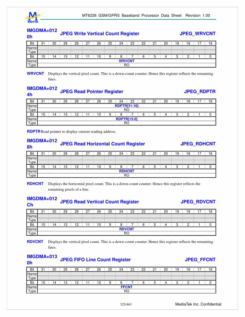
MT6226 GSM/GPRS Baseband Processor Data Sheet Revision 1.00
325/463 MediaTek Inc. Confidential
IMGDMA+0120h
JPEG Write Vertical Count Register JPEG_WRVCNT
Bit 31 30 29 28 27 26 25 24 23 22 21 20 19 18 17 16 Name Type Bit 15 14 13 12 11 10 9 8 7 6 5 4 3 2 1 0
Name WRVCNT Type RO
WRVCNT Displays the vertical pixel count. This is a down-count counter. Hence this register reflects the remaining
lines.
IMGDMA+0124h
JPEG Read Pointer Register JPEG_RDPTR
Bit 31 30 29 28 27 26 25 24 23 22 21 20 19 18 17 16 Name RDPTR[31:16] Type RO Bit 15 14 13 12 11 10 9 8 7 6 5 4 3 2 1 0
Name RDPTR[15:0] Type RO
RDPTR Read pointer to display current reading address.
IMGDMA+0128h
JPEG Read Horizontal Count Register JPEG_RDHCNT
Bit 31 30 29 28 27 26 25 24 23 22 21 20 19 18 17 16 Name Type Bit 15 14 13 12 11 10 9 8 7 6 5 4 3 2 1 0
Name RDHCNT Type RO
RDHCNT Displays the horizontal pixel count. This is a down-count counter. Hence this register reflects the
remaining pixels of a line.
IMGDMA+012Ch
JPEG Read Vertical Count Register JPEG_RDVCNT
Bit 31 30 29 28 27 26 25 24 23 22 21 20 19 18 17 16 Name Type Bit 15 14 13 12 11 10 9 8 7 6 5 4 3 2 1 0
Name RDVCNT Type RO
RDVCNT Displays the vertical pixel count. This is a down-count counter. Hence this register reflects the remaining
lines.
IMGDMA+0130h
JPEG FIFO Line Count Register JPEG_FFCNT
Bit 31 30 29 28 27 26 25 24 23 22 21 20 19 18 17 16 Name Type Bit 15 14 13 12 11 10 9 8 7 6 5 4 3 2 1 0
Name FFCNT Type RO

MT6226 GSM/GPRS Baseband Processor Data Sheet Revision 1.00
326/463 MediaTek Inc. Confidential
FFCNT Displays the FIFO Line Count of JPEG FIFO.
IMGDMA+0134h
JPEG Write Line Index Register JPEG_FFWRLI
DX Bit 31 30 29 28 27 26 25 24 23 22 21 20 19 18 17 16
Name Type Bit 15 14 13 12 11 10 9 8 7 6 5 4 3 2 1 0
Name YIDX Type RO
YIDX Displays which FIFO line JPEG DMA is writing. YIDX = 1 ~ FIFOLEN.
IMGDMA+0138h
JPEG Read Line Index Register JPEG_FFRDLID
X Bit 31 30 29 28 27 26 25 24 23 22 21 20 19 18 17 16
Name Type Bit 15 14 13 12 11 10 9 8 7 6 5 4 3 2 1 0
Name YIDX Type RO
YIDX Displays which FIFO line JPEG DMA is reading, YIDX = 1 ~ FIFOLEN.
IMGDMA+0200h
Video DMA Start Register VDO_STR
Bit 31 30 29 28 27 26 25 24 23 22 21 20 19 18 17 16 Name Type Reset
Bit 15 14 13 12 11 10 9 8 7 6 5 4 3 2 1 0 Name STR Type R/W Reset 0
This register controls the activity of a DMA channel. Note that before setting STR to “1”, all the configurations should be done by giving proper values.
STR Start control for a DMA channel 0 stop DMA 1 activate DMA
IMGDMA+0204h
Video DMA Control Register VDO_CON
Bit 31 30 29 28 27 26 25 24 23 22 21 20 19 18 17 16 Name Type Reset
Bit 15 14 13 12 11 10 9 8 7 6 5 4 3 2 1 0
Name AUTO RSTR
TWC IT TWC DIR DONE
IT Type R/W R/W R/W R/W R/W Reset 0 0 0 0 0

MT6226 GSM/GPRS Baseband Processor Data Sheet Revision 1.00
327/463 MediaTek Inc. Confidential
DONE IT DMA Done Interrupt Enabling. Interrupt issues when all of the transfers are done. For the application of twice resizing, interrupt will issue at the end of the second run, as illustrated in Figure 124. For auto-restart mode, interrupt issues at every restart.
First RUN Second RUN First RUN Second RUN
FrameBoundary
FrameBoundary
FrameBoundary
Figure 124 Interrupt Timing
0 Disable 1 Enable
DIR Direction of DMA 0 Video decoding. Video Buffer to Resizer. 1 Video encoding. Image Engine to Video Buffer.
TWC Twice Resizing. It is used when the frame size of LCD is different from the frame size of MPEG4 encoder. While this function is enabled, Video DMA will write data to video buffer first, and then read back from the same buffer. These data will pass through resizer again to convert to different frame size. At the end of Video write, a start pulse will issue to the two Image Buffer Write DMAs. If IBW DMAs are also enabled this function, they will wait for this signal to start data movement, otherwise this signal is useless for them. Once this function is enabled, DIR must be set 1. 0 Disable 1 Enable
TWC IT Twice Resizing Interrupt Enabling. This function only takes effect if Twice Resizing is enabled. Interrupt issues at the end of first run, as illustrated in . 0 Disable 1 Enable
AUTO RSTR Automatic restart. Video DMA automatically restarts while current frame is finished. Base address will be automatically switched between VDO_BSADD1 and VDO_BSADDR2. For single buffer application, please set VDO_BSADD1 and VDO_BSADDR2 with the same value. This function can be used with twice resizing. 0 Disable 1 Enable
IMGDMA+0208h
Video Base Address 1 Register VDO_BSADDR1
Bit 31 30 29 28 27 26 25 24 23 22 21 20 19 18 17 16 Name ADDR Type R/W Bit 15 14 13 12 11 10 9 8 7 6 5 4 3 2 1 0
Name ADDR Type R/W
ADDR First base address of video frame buffer.
IMGDMA+020Ch
Video Base Address 2 Register VDO_BSADDR2
Bit 31 30 29 28 27 26 25 24 23 22 21 20 19 18 17 16

MT6226 GSM/GPRS Baseband Processor Data Sheet Revision 1.00
328/463 MediaTek Inc. Confidential
Name ADDR Type R/W Bit 15 14 13 12 11 10 9 8 7 6 5 4 3 2 1 0
Name ADDR Type R/W
ADDR Second base address of video frame buffer.
IMGDMA+0210h
Video Horizontal Size Register VDO_HSIZE
Bit 31 30 29 28 27 26 25 24 23 22 21 20 19 18 17 16 Name Type Bit 15 14 13 12 11 10 9 8 7 6 5 4 3 2 1 0
Name SIZE Type R/W
SIZE Horizontal dimension of a video frame. 1 stands for 1 pixel, and n stands for n pixels. Note that the
horizontal size must be multiple of 16.
IMGDMA+0214h
Video Vertical Size Register VDO_VSIZE
Bit 31 30 29 28 27 26 25 24 23 22 21 20 19 18 17 16 Name Type Bit 15 14 13 12 11 10 9 8 7 6 5 4 3 2 1 0
Name SIZE Type R/W
SIZE Vertical dimension of a video frame. 1 stands for 1 pixel, and n stands for n pixels. Note that the vertical
size must be multiple of 16.
IMGDMA+0218h
Video Horizontal Count Register VDO_HCNT
Bit 31 30 29 28 27 26 25 24 23 22 21 20 19 18 17 16 Name Type Bit 15 14 13 12 11 10 9 8 7 6 5 4 3 2 1 0
Name COUNT Type RO
COUNT Horizontal pixel count. 1 stands for 1 pixel, and n stands for n pixels.
IMGDMA+021Ch
Video Vertical Count Register VDO_VCNT
Bit 31 30 29 28 27 26 25 24 23 22 21 20 19 18 17 16 Name Type Bit 15 14 13 12 11 10 9 8 7 6 5 4 3 2 1 0
Name COUNT Type RO
COUNT Vertical pixel count. 1 stands for 1 pixel, and n stands for n pixels.

MT6226 GSM/GPRS Baseband Processor Data Sheet Revision 1.00
329/463 MediaTek Inc. Confidential
IMGDMA+0300h
Image Buffer Write DMA1 Start Register IBW1_STR
Bit 31 30 29 28 27 26 25 24 23 22 21 20 19 18 17 16 Name Type Reset
Bit 15 14 13 12 11 10 9 8 7 6 5 4 3 2 1 0 Name STR Type R/W Reset 0
This register controls the activity of a DMA channel. Note that before setting STR to “1”, all the configurations should be done by giving proper values.
STR Start control for a DMA channel 0 stop DMA 1 activate DMA
IMGDMA+0304h
Image Buffer Write DMA1 Control Register IBW1_CON
Bit 31 30 29 28 27 26 25 24 23 22 21 20 19 18 17 16 Name Type Reset
Bit 15 14 13 12 11 10 9 8 7 6 5 4 3 2 1 0 Name IT Type R/W Reset 0
IT Interrupt Enabling
0 Disable 1 Enable
IMGDMA+0308h
Image Buffer Write DMA1 Base Address Register IBW1_BSADDR
Bit 31 30 29 28 27 26 25 24 23 22 21 20 19 18 17 16 Name ADDR Type R/W Bit 15 14 13 12 11 10 9 8 7 6 5 4 3 2 1 0
Name ADDR Type R/W
ADDR Base address of the image buffer.
IMGDMA+030Ch
Image Buffer Write DMA1 Number of Pixels Register IBW1_PXLNUM
Bit 31 30 29 28 27 26 25 24 23 22 21 20 19 18 17 16 Name NUM Type R/W Bit 15 14 13 12 11 10 9 8 7 6 5 4 3 2 1 0
Name NUM Type R/W
NUM Number of pixels of the transferred image. 0 represents 1 pixel, and n-1 represents n pixels.

MT6226 GSM/GPRS Baseband Processor Data Sheet Revision 1.00
330/463 MediaTek Inc. Confidential
IMGDMA+0310h
Image Buffer Write DMA1 Remaining Pixels Register IBW1_RMGPXL
Bit 31 30 29 28 27 26 25 24 23 22 21 20 19 18 17 16 Name NUM Type RO Bit 15 14 13 12 11 10 9 8 7 6 5 4 3 2 1 0
Name NUM Type RO
NUM Remaining pixel count. 0 represents 1 pixel, and n-1 represents n pixels.
IMGDMA+0400h
Image Buffer Write DMA2 Start Register IBW2_STR
Bit 31 30 29 28 27 26 25 24 23 22 21 20 19 18 17 16 Name Type Reset
Bit 15 14 13 12 11 10 9 8 7 6 5 4 3 2 1 0 Name STR Type R/W Reset 0
This register controls the activity of a DMA channel. Note that before setting STR to “1”, all the configurations should be done by giving proper value
STR Start control for a DMA channel 0 stop DMA 1 activate DMA
IMGDMA+0404h
Image Buffer Write DMA2 Control Register IBW2_CON
Bit 31 30 29 28 27 26 25 24 23 22 21 20 19 18 17 16 Name Type Reset
Bit 15 14 13 12 11 10 9 8 7 6 5 4 3 2 1 0
Name PAN DC AUTO RSTR LCD TWC IT
Type R/W R/W R/W R/W R/W R/W Reset 0 0 0 0 0 0
IT Interrupt Enabling
0 Disable 1 Enable
TWC Twice Resizing, which is used when the frame size of LCD is different from the frame size of MPEG4 encoder. Once the function is enabled, IBW2 DMA will wait for start pulse from video DMA to start data transfer. 0 Disable 1 Enable
LCD Signaling LCD DMA. Frame ready signal is issued at the beginning of frames in Direct Couple mode, and is issued at the end of frames in Dual Buffer mode. Note that in the case of automatic restart plus direct couple mode, this function must be enabled to trigger LCD DMA. 0 Disable 1 Enable

MT6226 GSM/GPRS Baseband Processor Data Sheet Revision 1.00
331/463 MediaTek Inc. Confidential
AUTO RSTR Automatic restart. IBW2 DMA automatically restarts itself while current frame is finished. 0 Disable 1 Enable
DC Directly coupling to LCD DMA. Once this function is enabled, image data will dump to LCD DMA directly instead of dumping to LCD frame buffer. 0 Disable 1 Enable
PAN Picture panning. Once this function is enabled, only the pixels in the region specified by HPITCH1, HPITCH2, VPITCH1, and VPITCH2 are dumped. The PITCHs are defined as Figure 125.
HPITCH1 HPITCH2
VPITCH1
VPITCH2
Figure 125 Picture Panning
0 Disable 1 Enable
IMGDMA+0408h
Image Buffer Write DMA2 Base Address 1 Register IBW2_BSADDR
1 Bit 31 30 29 28 27 26 25 24 23 22 21 20 19 18 17 16
Name ADDR Type R/W Bit 15 14 13 12 11 10 9 8 7 6 5 4 3 2 1 0
Name ADDR Type R/W
ADDR First base address of the LCD frame buffer.
IMGDMA+040Ch
Image Buffer Write DMA2 Base Address 2 Register IBW2_BSADDR
2 Bit 31 30 29 28 27 26 25 24 23 22 21 20 19 18 17 16
Name ADDR Type R/W Bit 15 14 13 12 11 10 9 8 7 6 5 4 3 2 1 0
Name ADDR Type R/W
ADDR Second base address of the LCD frame buffer.
IMGDMA+0410h
Image Buffer Write DMA2 Horizontal Size Register IBW2_HSIZE
Bit 31 30 29 28 27 26 25 24 23 22 21 20 19 18 17 16

MT6226 GSM/GPRS Baseband Processor Data Sheet Revision 1.00
332/463 MediaTek Inc. Confidential
Name Type Bit 15 14 13 12 11 10 9 8 7 6 5 4 3 2 1 0
Name SIZE Type R/W
SIZE Horizontal size of a frame. 0 stands for 1 pixel, and n-1 stands for n pixels.
IMGDMA+0414h
Image Buffer Write DMA2 Vertical Size Register IBW2_VSIZE
Bit 31 30 29 28 27 26 25 24 23 22 21 20 19 18 17 16 Name Type Bit 15 14 13 12 11 10 9 8 7 6 5 4 3 2 1 0
Name SIZE Type R/W
SIZE Vertical size of a frame. 0 stands for 1 pixel, and n-1 stands for n pixels.
IMGDMA+0418h
Image Buffer Write DMA2 Horizontal Pitch1 Register IBW2_HPITCH1
Bit 31 30 29 28 27 26 25 24 23 22 21 20 19 18 17 16 Name Type Bit 15 14 13 12 11 10 9 8 7 6 5 4 3 2 1 0
Name PITCH Type R/W
PITCH First horizontal pitch of a frame. 0 stands for the first pixel, and n-1 stands for the nth pixel.
IMGDMA+041Ch
Image Buffer Write DMA2 Horizontal Pitch2 Register IBW2_HPITCH2
Bit 31 30 29 28 27 26 25 24 23 22 21 20 19 18 17 16 Name Type Bit 15 14 13 12 11 10 9 8 7 6 5 4 3 2 1 0
Name PITCH Type R/W
PITCH Second horizontal pitch of a frame. 0 stands for the first pixel, and n-1 stands for the nth pixel.
IMGDMA+0420h
Image Buffer Write DMA2 Vertical Pitch1 Register IBW2_VPITCH1
Bit 31 30 29 28 27 26 25 24 23 22 21 20 19 18 17 16 Name Type Bit 15 14 13 12 11 10 9 8 7 6 5 4 3 2 1 0
Name PITCH Type R/W
PITCH First vertical pitch of a frame. 0 stands for the first pixel, and n-1 stands for the nth pixels.
IMGDMA+0424h
Image Buffer Write DMA2 Vertical Pitch2 Register IBW2_VPITCH2
Bit 31 30 29 28 27 26 25 24 23 22 21 20 19 18 17 16 Name

MT6226 GSM/GPRS Baseband Processor Data Sheet Revision 1.00
333/463 MediaTek Inc. Confidential
Type Bit 15 14 13 12 11 10 9 8 7 6 5 4 3 2 1 0
Name PITCH Type R/W
PITCH Second vertical pitch of a frame. 0 stands for the first pixel, and n-1 stands for the nth pixels.
IMGDMA+0428h
Image Buffer Write DMA2 Horizontal Count Register IBW2_HCNT
Bit 31 30 29 28 27 26 25 24 23 22 21 20 19 18 17 16 Name Type Bit 15 14 13 12 11 10 9 8 7 6 5 4 3 2 1 0
Name CNT Type RO
CNT Horizontal pixel count. 0 stands for 1 pixel, and n-1 stands for n pixels.
IMGDMA+042Ch
Image Buffer Write DMA2 Vertical Count Register IBW2_VCNT
Bit 31 30 29 28 27 26 25 24 23 22 21 20 19 18 17 16 Name Type Bit 15 14 13 12 11 10 9 8 7 6 5 4 3 2 1 0
Name CNT Type RO
CNT Vertical line count. 0 stands for 1 line, and n-1 stands for n lines.
IMGDMA+0500h
Image Buffer Read DMA1 Start Register IBR1_STR
Bit 31 30 29 28 27 26 25 24 23 22 21 20 19 18 17 16 Name Type Reset
Bit 15 14 13 12 11 10 9 8 7 6 5 4 3 2 1 0 Name STR Type R/W Reset 0
This register controls the activity of a DMA channel. Note that before setting STR to “1”, all the configurations should be done by giving proper values.
STR Start control for a DMA channel 0 stop DMA 1 activate DMA
IMGDMA+0504h
Image Buffer Read DMA1 Control Register IBR1_CON
Bit 31 30 29 28 27 26 25 24 23 22 21 20 19 18 17 16 Name Type Reset
Bit 15 14 13 12 11 10 9 8 7 6 5 4 3 2 1 0
Name ORDER FMT IT
Type R/W R/W R/W

MT6226 GSM/GPRS Baseband Processor Data Sheet Revision 1.00
334/463 MediaTek Inc. Confidential
Reset 0 0 0
IT Interrupt Enabling 0 Disable 1 Enable
FMT Data format 0 RGB565 1 RGB888
ORDER Data order 0 BGR888, from MSB to LSB. 1 RGB888, from MSB to LSB.
IMGDMA+0508h
Image Buffer Read DMA1 Base Address Register IBR1_BSADDR
Bit 31 30 29 28 27 26 25 24 23 22 21 20 19 18 17 16 Name ADDR Type R/W Bit 15 14 13 12 11 10 9 8 7 6 5 4 3 2 1 0
Name ADDR Type R/W
ADDR Base address of the image buffer.
IMGDMA+050Ch
Image Buffer Read DMA1 Number of Pixels Register IBR1_PXLNUM
Bit 31 30 29 28 27 26 25 24 23 22 21 20 19 18 17 16 Name NUM Type R/W Bit 15 14 13 12 11 10 9 8 7 6 5 4 3 2 1 0
Name NUM Type R/W
NUM Number of pixels of the transferred image. 0 represents 1 pixel, and n-1 represents n pixels.
IMGDMA+0510h
Image Buffer Read DMA1 Remaining Pixels Register IBR1_PXLCNT
Bit 31 30 29 28 27 26 25 24 23 22 21 20 19 18 17 16 Name COUNT Type RO Bit 15 14 13 12 11 10 9 8 7 6 5 4 3 2 1 0
Name COUNT Type RO
COUNT Pixel count. 0 represents 1 pixel, and n-1 represents n pixels.
6.12 Image Engine The Image Engine is used to manipulate image adjustments and a variety of filtering effects. It works inside the DMA architecture, which minimizes the intervention of the CPU. The engine can directly access the external and internal memories and provide a large extent of flexibility for system performance consideration.
The function of the engine basically contains two categories: pixel adjustment and filtering effect.

MT6226 GSM/GPRS Baseband Processor Data Sheet Revision 1.00
335/463 MediaTek Inc. Confidential
Pixel adjustment includes brightness, contrast, and hue adjustment, color adjustment, and gamma correction. These effects are integrated on both the encoding and decoding path of image and video material. It can provide on-the-fly manipulation on these raw materials. For camera preview and capture, it can perform the effects on the incoming image frame immediately, and output to both frame buffer for display and image buffer for image compression. For video playback, it can perform the effects on the decoded frame immediately and output to the frame buffer for display.
The filtering effect includes linear and non-linear (ranking) effects. The linear filtering provides blur and sharpening effects with programmable mask design. The non-linear filtering provides ranking filter to emulate noise reduction, dilation and erosion effects. We can also implement other artistic effects by performing multi-pass filtering with combination of a variety of effects.
6.12.1 Register Definitions
Register Address Register Function Acronym
IMG+0000h Image flow control register IMGPROC_IMAGE_CON IMG+0004h Control register IMGPROC_CON IMG+0008h Interrupt enable register IMGPROC_INTREN IMG+000Ch Interrupt status register IMGPROC_INTR IMG+0010h Status register IMGPROC_STATUS IMG+0100h Hue adjustment coefficient C11 IMGPROC_HUE11 IMG+0104h Hue adjustment coefficient C12 IMGPROC_HUE12 IMG+0108h Hue adjustment coefficient C21 IMGPROC_HUE21 IMG+010Ch Hue adjustment coefficient C22 IMGPROC_HUE22 IMG+0110h Saturation adjustment coefficient IMGPROC_SAT IMG+0120h Brightness adjustment coefficient B1 IMGPROC_BRIADJ1 IMG+0124h Brightness adjustment coefficient B2 IMGPROC_BRIADJ2 IMG+0128h Contrast adjustment coefficient IMGPROC_CONADJ IMG+0130h Colorize effect coefficient IMGPROC_COLORIZEU IMG+0134h Colorize effect coefficient IMGPROC_COLORIZEV IMG+0140h Mask coefficient C11 IMGPROC_MASK11 IMG+0144h Mask coefficient C12 IMGPROC_MASK12 IMG+0148h Mask coefficient C13 IMGPROC_MASK13 IMG+014Ch Mask coefficient C21 IMGPROC_MASK21 IMG+0150h Mask coefficient C22 IMGPROC_MASK22 IMG+0154h Mask coefficient C23 IMGPROC_MASK23 IMG+0158h Mask coefficient C31 IMGPROC_MASK31 IMG+015Ch Mask coefficient C32 IMGPROC_MASK32 IMG+0160h Mask coefficient C33 IMGPROC_MASK33 IMG+0164h Mask down-scaling coefficient IMGPROC_SCALE IMG+0170h Gamma correction offset for segment 0 IMGPROC_GAMMA_OFF0 IMG+0174h Gamma correction offset for segment 1 IMGPROC_GAMMA_OFF1 IMG+0178h Gamma correction offset for segment 2 IMGPROC_GAMMA_OFF2 IMG+017Ch Gamma correction offset for segment 3 IMGPROC_GAMMA_OFF3 IMG+0180h Gamma correction offset for segment 4 IMGPROC_GAMMA_OFF4

MT6226 GSM/GPRS Baseband Processor Data Sheet Revision 1.00
336/463 MediaTek Inc. Confidential
IMG+0184h Gamma correction offset for segment 5 IMGPROC_GAMMA_OFF5 IMG+0188h Gamma correction offset for segment 6 IMGPROC_GAMMA_OFF6 IMG+018Ch Gamma correction offset for segment 7 IMGPROC_GAMMA_OFF7 IMG+0190h Gamma correction slope for segment 0 IMGPROC_GAMMA_SLP0 IMG+0194h Gamma correction slope for segment 1 IMGPROC_GAMMA_SLP1 IMG+0198h Gamma correction slope for segment 2 IMGPROC_GAMMA_SLP2 IMG+019Ch Gamma correction slope for segment 3 IMGPROC_GAMMA_SLP3 IMG+01A0h Gamma correction slope for segment 4 IMGPROC_GAMMA_SLP4 IMG+01A4h Gamma correction slope for segment 5 IMGPROC_GAMMA_SLP5 IMG+01A8h Gamma correction slope for segment 6 IMGPROC_GAMMA_SLP6 IMG+01ACh Gamma correction slope for segment 7 IMGPROC_GAMMA_SLP7 IMG+01B0h Gamma correction control register IMGPROC_GAMMA_CON IMG+0200h Color adjustment offset x for red segment 1 IMGPROC_COLOR1R_OFFX IMG+0204h Color adjustment offset x for red segment 2 IMGPROC_COLOR2R_OFFX IMG+0208h Color adjustment offset x for green segment 1 IMGPROC_COLOR1G_OFFX IMG+020Ch Color adjustment offset x for green segment 2 IMGPROC_COLOR2G_OFFX IMG+0210h Color adjustment offset x for blue segment 1 IMGPROC_COLOR1B_OFFX IMG+0214h Color adjustment offset x for blue segment 2 IMGPROC_COLOR2B_OFFX IMG+0220h Color adjustment offset y for red segment 1 IMGPROC_COLOR1R_OFFY IMG+0224h Color adjustment offset y for red segment 2 IMGPROC_COLOR2R_OFFY IMG+0228h Color adjustment offset y for green segment 1 IMGPROC_COLOR1G_OFFY IMG+022Ch Color adjustment offset y for green segment 2 IMGPROC_COLOR2G_OFFY IMG+0230h Color adjustment offset y for blue segment 1 IMGPROC_COLOR1B_OFFY IMG+0234h Color adjustment offset y for blue segment 2 IMGPROC_COLOR2B_OFFY IMG+0240h Color adjustment slope for red segment 0 IMGPROC_COLOR1G_SLP IMG+0244h Color adjustment slope for red segment 1 IMGPROC_COLOR1G_SLP IMG+0248h Color adjustment slope for red segment 2 IMGPROC_COLOR2G_SLP IMG+0250h Color adjustment slope for red segment 0 IMGPROC_COLOR1G_SLP IMG+0254h Color adjustment slope for red segment 1 IMGPROC_COLOR1G_SLP IMG+0258h Color adjustment slope for red segment 2 IMGPROC_COLOR2G_SLP IMG+0260h Color adjustment slope for red segment 0 IMGPROC_COLOR1G_SLP IMG+0264h Color adjustment slope for red segment 1 IMGPROC_COLOR1G_SLP IMG+0268h Color adjustment slope for red segment 2 IMGPROC_COLOR2G_SLP IMG+0304h Image frame width register IMGPROC_IMGWIDTH IMG+0308h Image frame height register IMGPROC_IMGHEIGHT IMG+030Ch Image frame source start address IMGPROC_ADDR_SRC IMG+0310h Image frame destination start address IMGPROC_ADDR_DST IMG+0314h Image frame filtering dummy pixel IMGPROC_DUMMYPXL IMG+0318h Image engine reset IMGPROC_RESET
Table 56 Image Engine Registers

MT6226 GSM/GPRS Baseband Processor Data Sheet Revision 1.00
337/463 MediaTek Inc. Confidential
IMG+0000h Image Engine image flow control register IMGPROC_IMA
GE_CON Bit 15 14 13 12 11 10 9 8 7 6 5 4 3 2 1 0
Name GMODE MASK GMA CLR INV CBA HSA Type R/W R/W R/W R/W R/W R/W R/W Reset 0 0 0 0 0 0 0
This register is used to define which effects are to be applied on the video stream or on the stand-alone image. The user can simply set this register to 0 if intended to bypass Image Engine.
The MSB 4 bits controls the operating mode and image flow of the engine. They should be set prior to enabling the respective functions; and when all are equal to 0, no operation will take effect.
The MASK field defines which mask filtering effect is to be applied. In these filtering effects, the image source data must be read from one image buffer and then written to another image buffer. The effects comprise of linear and non-linear effects. Some linear effects, such as Low-pass, High-pass, un-sharpening effects, should be associated with the mask table, therefore the user should program the mask coefficients. The LP (low-pass) filter provides smoothing effects. Since it is supposed to get un-biased data, the convolution will be normalized to its original intensity. The HP (high-pass) filter, which provides sharpening effects, does not necessarily produce un-biased data. We provide two HP filters, one with scaling factor and the other without. Depending on what mask type is defined, the result may reveal only edge information or may keep the average intensity to achieve the sharpening effects. We recommend using symmetrical form of mask.
In addition to 3x3 masks, 5x5 and 7x7 masks are also provided. But only the blur effects are provided for the later two effects. The user does not have to program the mask coefficients.
The LSB 7 bits controls all the pixel adjustment effect. The image source data for the pixel adjustment must be from RESIZER and output to IMGDMA..
For gamma correction and color adjustment, which are to be performed on RGB color space, the Image Engine provides piece-wise linear programming mechanism. The user should know the slope and offset of respective segments.
Color invert effect, performed on YUV or RGB color spaces, provides negative film effects.
Contrast and brightness, hue and saturation effects are to be performed on YUV color space. Although, the user can also do post-processing on the image prepared in RGB form. The Image Engine can convert it into YUV space for those operations.
GMODE Graph mode. The field defines the image flow in each case. 1000 Image Encode mode. (RGB to YUV) In this mode, the Image Engine performs the color space
conversion from RGB color space to YUV color space. This mode is mainly used for image encoding, such as JPEG encoding. In this mode, we assume no image effects are to be applied.
0100 Image effect mode. (RGB to RGB) In this mode, the Image Engine applies image effects on the stand-alone image. The data source and destination is supposed to be in RGB color space. In this mode, the user should program image size and related information on image DMA. The image DMA retrieves image, performs image effects on Image Engine, and then writes to the memory.
0011 MPEG encode mode. (YUV to YUV, then RGB) In this mode, the image is converted from YUV color space to both YUV and RGB color space with different image dimensions. The pixel in YUV is for encoding, while that in RGB is for displaying. In this mode, we assume no image effects are to be performed in Image Engine. The user can adjust the image quality by programming ISP.
0010 Capture mode. (YUV to YUV) In this mode, the captured image in YUV color space and is not performed color space conversion. This mode is mainly used for image capture.

MT6226 GSM/GPRS Baseband Processor Data Sheet Revision 1.00
338/463 MediaTek Inc. Confidential
0001 Playback mode. (YUV to RGB) In this mode, the Image Engine performs the color space conversion from YUV color space to RGB color space. This mode is mainly used for preview, image playback, and video playback.
MASK Mask filtering effect enabling control . 0101 Linear LP (low-pass) filtering effect enable. Mask coefficients required. 0110 Linear HP (high-pass) filtering effect enable. Mask coefficients required. 0111 Linear HP filtering (with scale down) effect enable. Mask coefficients required. 1001 Blur effect enable. (5x5 mask) 1010 More blur effect enable. (7x7 mask) 1011 Un-sharp mask effect enable. Mask coefficients required. 1100 Maximum ranking (dilation) filter effect enable 1101 Median ranking filter effect enable 1110 Minimum ranking (erosion) filter effect enable
GMA Gamma correction enable bit CLR Color adjustment enable bit INV Color invert enable bit (This effect can not exist individually) CBA Contrast and brightness adjustment enable bit HSA Hue and saturation adjustment enable
001 Gray-scale effect enable 010 Colorize effect enable 101 Hue adjustment enable 110 Saturation adjustment enable 111 Hue and saturation adjustment enable
Note: before starting image effect operations, the coefficients of other image processes need to be initialized.
IMG+0004h Mask filtering Control register IMGPROC_CON Bit 15 14 13 12 11 10 9 8 7 6 5 4 3 2 1 0
Name STOP START
Type WO WO Reset 0 0
This register is used to control the filtering process and coefficients setting. STOP Writing logic-1 stops the image filter processing. The flag is write-only. START Writing logic-1 starts the image filter processing. The flag is write-only.
IMG+0008h Interrupt enable register IMGPROC_INTR
EN Bit 15 14 13 12 11 10 9 8 7 6 5 4 3 2 1 0
Name EN Type R/W Reset 0
This register is the interrupt enable control register. To enable the interrupt, the flag should be set to be 1. EN Interrupt enable flag.
IMG +000Ch Interrupt status register IMGPROC_INTR Bit 15 14 13 12 11 10 9 8 7 6 5 4 3 2 1 0
Name INTR Type RC Reset 0

MT6226 GSM/GPRS Baseband Processor Data Sheet Revision 1.00
339/463 MediaTek Inc. Confidential
This register is the interrupt status register. The core set the flag to be 1 to represent the interrupt is asserted. Reading this register will clear the interrupt.
INTR Interrupt status flag. The flag is read-clear.
IMG +0010h Status register IMGPROC_STS Bit 15 14 13 12 11 10 9 8 7 6 5 4 3 2 1 0
Name FLR_GLCO
MD
FLR_GRDY
FLR_GREQ
FLR_BUSY PIXEL
_ACK PIXEL_REQ
PIXELBUSY
Type RO Reset 0
This register is the status register. The user could poll this register to see if the filtering process is ready or not. The flag is read-only. PIXEL_BUSY Pixel-based operation is in process. PIXEL_REQ Pixel-based data output request. PIXEL_ACK Pixel-based data output acknowledgement. FLR_BUSY Filtering is in process. FLR_GREQ GMC bus request. FLR_GRDY GMC data ready FLR_GLCOMD GMC command latch
IMG+0100h Hue adjustment coefficient C11 IMGPROC_HUE
11 Bit 15 14 13 12 11 10 9 8 7 6 5 4 3 2 1 0
Name C11 Type R/W Reset 40h
IMG+0104h Hue adjustment coefficient C12 IMGPROC_HUE
12 Bit 15 14 13 12 11 10 9 8 7 6 5 4 3 2 1 0
Name C12 Type R/W Reset 0
IMG+0108h Hue adjustment coefficient C21 IMGPROC_HUE
21 Bit 15 14 13 12 11 10 9 8 7 6 5 4 3 2 1 0
Name C21 Type R/W Reset 0
IMG+010Ch Hue adjustment coefficient C22 IMGPROC_HUE
22 Bit 15 14 13 12 11 10 9 8 7 6 5 4 3 2 1 0
Name C22 Type R/W Reset 40h

MT6226 GSM/GPRS Baseband Processor Data Sheet Revision 1.00
340/463 MediaTek Inc. Confidential
This register controls the parameter of hue adjustment for the image. The effect is performed on the U and V component of YUV color space. The user should specify the coefficients that form the transformation matrix. The formula is listed as follows:
θθθθ cos6422,sin6421,sin6412,cos6411
222112110
=−===
⋅
=
CCCCwhere
v
u
CC
CCv
u
i
i
o
The coefficients are in 2’s complement format and range from C0h to 40h (from –64 to 64 in decimal, while 64 is normalized to 1 corresponding to cosine values). Any value beyond this range is invalid.
For example, to rotate the color space counterclockwise by 30 degree, the coefficients should be 37h, 20h, e0h, and 37h.
C11 The coefficient C11 of the transformation matrix in 2’s complement format. C12 The coefficient C12 of the transformation matrix in 2’s complement format. C21 The coefficient C21 of the transformation matrix in 2’s complement format. C22 The coefficient C22 of the transformation matrix in 2’s complement format.
IMG+0110h Saturation adjustment coefficient IMGPROC_SAT
ADJ Bit 15 14 13 12 11 10 9 8 7 6 5 4 3 2 1 0
Name SAT Type R/W Reset 20h
This register defines the parameter of saturation adjustment for the image. The basics of saturation tuning is to multiply the U and V component by a scaling factor, which could range from 0 to 255, to degrade or enhance the strength on color components. Setting to 20h represents no scaling. SAT Saturation coefficient.
IMG+0120h Brightness adjustment coefficient B1 IMGPROC_BRI
ADJ1 Bit 15 14 13 12 11 10 9 8 7 6 5 4 3 2 1 0
Name BRI Type R/W Reset 0
This register defines the parameter of brightness adjustment for the image. The parameter is in unsigned format. Setting the value to be greater than 0 adds to the intensity of the image pixel. In terms of transfer curve, it represents the offset in the y-axis. The valid value ranges from 0 to 255. BRI Brightness adjustment coefficient.
IMG+0124h Brightness adjustment coefficient B2 IMGPROC_BRI
ADJ2 Bit 15 14 13 12 11 10 9 8 7 6 5 4 3 2 1 0
Name DRK Type R/W Reset 0
This register controls the parameter of brightness adjustment for the image. The parameter is in unsigned format. Setting the value to be greater than 0 degrades the intensity of the image pixel. In terms of transfer curve, it represents the offset in the x-axis. The valid value ranges from 0 to 255.

MT6226 GSM/GPRS Baseband Processor Data Sheet Revision 1.00
341/463 MediaTek Inc. Confidential
DRK Brightness adjustment coefficient
IMG+0128h Contrast adjustment coefficient IMGPROC_CON
ADJ Bit 15 14 13 12 11 10 9 8 7 6 5 4 3 2 1 0
Name CON Type R/W Reset 20h
This register defines the parameter of contrast adjustment for the image pixel. The parameter is in unsigned format with normalization factor 20h. Setting the value to be greater than 20h enhances the contrast for the image; and setting the value to be less than 20h lowers the contrast for the image. The valid value ranges from 0 to 255.
CON Contrast adjustment coefficient
IMG+0130h Colorize u component coefficient IMGPROC_COL
ORIZEU Bit 15 14 13 12 11 10 9 8 7 6 5 4 3 2 1 0
Name UCOM Type R/W Reset 0
IMG+0134h Colorize v component coefficient IMGPROC_COL
ORIZEV Bit 15 14 13 12 11 10 9 8 7 6 5 4 3 2 1 0
Name VCOM Type R/W Reset 0
These registers controls the parameters of colorize effect for the image. The valid value ranges from –128 to 127 in 2’s complement format. If the values of both coefficients are zero, it implies the gray-scale effect.
UCOM Colorize effect u component coefficient. VCOM Colorize effect v component coefficient.
IMG+0140h Mask coefficient C11 IMGPROC_MAS
K11 Bit 15 14 13 12 11 10 9 8 7 6 5 4 3 2 1 0
Name C11 Type R/W Reset 0
IMG+0144h Mask coefficient C12 IMGPROC_MAS
K12 Bit 15 14 13 12 11 10 9 8 7 6 5 4 3 2 1 0
Name C12 Type R/W Reset 0
IMG+0148h Mask coefficient C13 IMGPROC_MAS
K13 Bit 15 14 13 12 11 10 9 8 7 6 5 4 3 2 1 0

MT6226 GSM/GPRS Baseband Processor Data Sheet Revision 1.00
342/463 MediaTek Inc. Confidential
Name C13 Type R/W Reset 0
IMG+014Ch Mask coefficient C21 IMGPROC_MAS
K21 Bit 15 14 13 12 11 10 9 8 7 6 5 4 3 2 1 0
Name C21 Type R/W Reset 0
IMG+0150h Mask coefficient C22 IMGPROC_MAS
K22 Bit 15 14 13 12 11 10 9 8 7 6 5 4 3 2 1 0
Name C22 Type R/W Reset 0
IMG+0154h Mask coefficient C23 IMGPROC_MAS
K23 Bit 15 14 13 12 11 10 9 8 7 6 5 4 3 2 1 0
Name C23 Type R/W Reset 0
IMG+0158h Mask coefficient C31 IMGPROC_MAS
K31 Bit 15 14 13 12 11 10 9 8 7 6 5 4 3 2 1 0
Name C31 Type R/W Reset 0
IMG+015Ch Mask coefficient C32 IMGPROC_MAS
K32 Bit 15 14 13 12 11 10 9 8 7 6 5 4 3 2 1 0
Name C32 Type R/W Reset 0
IMG+0160h Mask coefficient C33 IMGPROC_MAS
K33 Bit 15 14 13 12 11 10 9 8 7 6 5 4 3 2 1 0
Name C33 Type R/W Reset 0
These registers define the 9 mask coefficients for linear filtering. The coefficients are in 2’s complement format with range from –16 to 15. The index associated with these coefficients represents the row index followed by the column index. The Image Engine performs the same arithmetic convolution on 3 components of the target image.

MT6226 GSM/GPRS Baseband Processor Data Sheet Revision 1.00
343/463 MediaTek Inc. Confidential
333231232221
131211
CCC
CCC
CCC
C11 Mask coefficient C11. C12 Mask coefficient C12. C13 Mask coefficient C13. C21 Mask coefficient C21. C22 Mask coefficient C22. C23 Mask coefficient C23. C31 Mask coefficient C31. C32 Mask coefficient C32. C33 Mask coefficient C33
IMG+0164h Mask data down-scaling coefficient IMGPROC_SCA
LE Bit 15 14 13 12 11 10 9 8 7 6 5 4 3 2 1 0
Name SCA Type R/W Reset 0
This register stores the value that could divide the mask data after convolution. It’s used for normalization, and only for linear HP mode. SCA The value used to scale down the mask data.
IMG+0170h Gamma correction offset value for segment 0 IMGPROC_GAM
MA_OFF0 Bit 15 14 13 12 11 10 9 8 7 6 5 4 3 2 1 0
Name OFF0 Type R/W Reset 0
This register stores the y-offset value of the segment 0 for gamma correction.
OFF0 Offset value.
For offset values of other segments, please refer to Table 57.
IMG+0190h Gamma correction slope value for segment 0 IMGPROC_GAM
MA_SLP0 Bit 15 14 13 12 11 10 9 8 7 6 5 4 3 2 1 0
Name SLP0 Type R/W Reset 0
This register stores the slope value of the segment 0 for gamma correction.
SLP0 Slope value.
For slope values of other segments, please refer to Table 57.

MT6226 GSM/GPRS Baseband Processor Data Sheet Revision 1.00
344/463 MediaTek Inc. Confidential
IMG+01B0h Gamma correction control register IMGPROC_GAM
MA_CON Bit 15 14 13 12 11 10 9 8 7 6 5 4 3 2 1 0
Name GTO Type R/W Reset 0
This register is used to control the gamma correction mode. GTO gamma value greater than one indicator
0 Gamma value is not greater than one. 1 Gamma value is greater than one.
Register Address Register Function Acronym
IMG+0170h Offset value for the 1st segment IMGPROC_GAMMA_OFF0
IMG+0174h Offset value for the 2nd segment IMGPROC_GAMMA_OFF1
IMG+0178h Offset value for the 3rd segment IMGPROC_GAMMA_OFF2
IMG+017Ch Offset value for the 4th segment IMGPROC_GAMMA_OFF3
IMG+0180h Offset value for the 5th segment IMGPROC_GAMMA_OFF4
IMG+0184h Offset value for the 6th segment IMGPROC_GAMMA_OFF5
IMG+0188h Offset value for the 7th segment IMGPROC_GAMMA_OFF6
IMG+018Ch Offset value for the 8th segment IMGPROC_GAMMA_OFF7
IMG+0190h Slope value for the 1st segment IMGPROC_GAMMA_SLP0
IMG+0194h Slope value for the 2nd segment IMGPROC_GAMMA_SLP1
IMG+0198h Slope value for the 3rd segment IMGPROC_GAMMA_SLP2
IMG+019Ch Slope value for the 4th segment IMGPROC_GAMMA_SLP3
IMG+01A0h Slope value for the 5th segment IMGPROC_GAMMA_SLP4
IMG+01A4h Slope value for the 6th segment IMGPROC_GAMMA_SLP5
IMG+01A8h Slope value for the 7th segment IMGPROC_GAMMA_SLP6
IMG+01ACh Slope value for the 8th segment IMGPROC_GAMMA_SLP7
Table 57 Gamma correction offset and slope register list
IMG+0200h Color adjustment offset x for 2nd segment, red IMGPROC_COL
OR1R_OFFX Bit 15 14 13 12 11 10 9 8 7 6 5 4 3 2 1 0
Name OFFX Type R/W Reset 0
IMG+0220h Color adjustment offset y for 2nd segment, red IMGPROC_COL
OR1R_OFFY Bit 15 14 13 12 11 10 9 8 7 6 5 4 3 2 1 0
Name OFFY Type R/W Reset 0

MT6226 GSM/GPRS Baseband Processor Data Sheet Revision 1.00
345/463 MediaTek Inc. Confidential
IMG+0240h Color adjustment slope for 2nd segment, red IMGPROC_COL
OR1R_SLP Bit 15 14 13 12 11 10 9 8 7 6 5 4 3 2 1 0
Name SLP Type R/W Reset 0
The above lists part of the registers that define the color adjustment parameters. Color adjustment in Image Engine is used to tune the red, green, and blue color dimension individually to exhibit required color tone as a whole. We provide 3-segment piecewise linear transfer curve for the user to be configured. The x offset defines the separation point for input color value. The y offset defines the offset for each segment. The slope defines the contrast enhancement ratio for each segment. For the red and blue components, the bit-width of the offset value is 5. For green, the bit-width of the offset value is 6. For slope of 3 color components, the bit-width is 6. OFFX input value separation point. OFFY output value offset. SLP Slope. Contrast tuning ratio within the segment.
For all the registers of color adjustment, please refer to Table 12 for detail information.
Register Address Register Function Bit-width Acronym
IMG+0200h Color adjustment offset x for 2nd segment, red 5 IMGPROC_COLOR1R_OFFX
IMG+0204h Color adjustment offset x for 3rd segment, red 5 IMGPROC_COLOR2R_OFFX
IMG+0208h Color adjustment offset x for 2nd segment, green 6 IMGPROC_COLOR1G_OFFX
IMG+020Ch Color adjustment offset x for 3rd segment, green 6 IMGPROC_COLOR2G_OFFX
IMG+0210h Color adjustment offset x for 2nd segment, blue 5 IMGPROC_COLOR1R_OFFX
IMG+0214h Color adjustment offset x for 3rd segment, blue 5 IMGPROC_COLOR2R_OFFX
IMG+0220h Color adjustment offset y for 2nd segment, red 5 IMGPROC_COLOR1R_OFFY
IMG+0224h Color adjustment offset y for 3rd segment, red 5 IMGPROC_COLOR2R_OFFY
IMG+0228h Color adjustment offset y for 2nd segment, green 6 IMGPROC_COLOR1G_OFFY
IMG+022Ch Color adjustment offset y for 3rd segment, green 6 IMGPROC_COLOR2G_OFFY
IMG+0230h Color adjustment offset y for 2nd segment, blue 5 IMGPROC_COLOR1R_OFFY
IMG+0234h Color adjustment offset y for 3rd segment, blue 5 IMGPROC_COLOR2R_OFFY
IMG+0240h Color adjustment slope for 1st segment, red 6 IMGPROC_COLOR0R_SLOPE
IMG+0244h Color adjustment slope for 2nd segment, red 6 IMGPROC_COLOR1R_SLOPE
IMG+0248h Color adjustment slope for 3rd segment, red 6 IMGPROC_COLOR1R_SLOPE
IMG+0250h Color adjustment slope for 1st segment, green 6 IMGPROC_COLOR0G_SLOPE
IMG+0254h Color adjustment slope for 2nd segment, green 6 IMGPROC_COLOR1G_SLOPE
IMG+0258h Color adjustment slope for 3rd segment, green 6 IMGPROC_COLOR1G_SLOPE
IMG+0260h Color adjustment slope for 1st segment, blue 6 IMGPROC_COLOR0B_SLOPE
IMG+0264h Color adjustment slope for 2nd segment, blue 6 IMGPROC_COLOR1B_SLOPE
IMG+0268h Color adjustment slope for 3rd segment, blue 6 IMGPROC_COLOR1B_SLOPE
Table 58 Color adjustment offset and slope register list

MT6226 GSM/GPRS Baseband Processor Data Sheet Revision 1.00
346/463 MediaTek Inc. Confidential
IMG+0304h Image frame width IMGPROC_IMG
WIDTH Bit 15 14 13 12 11 10 9 8 7 6 5 4 3 2 1 0
Name IM Type R/W Reset 0
This register is the image frame width register. The maximum allowable frame width is 2047. The Image Engine uses it to locate the address for every pixel in the image frame. IM Image frame width
IMG+0308h Image frame height IMGPROC_IMG
HEIGHT Bit 15 14 13 12 11 10 9 8 7 6 5 4 3 2 1 0
Name IH Type R/W Reset 0
This register is the image frame height register. The maximum allowable frame height is 2047. The Image Engine uses it to locate the address for every pixel in the image frame. IH Image frame width
IMG+030Ch Image frame source register IMGPROC_ADD
R_SRC Bit 31 30 29 28 27 26 25 24 23 22 21 20 19 18 17 16
Name SRC[31:16] Type R/W Reset 0
Bit 15 14 13 12 11 10 9 8 7 6 5 4 3 2 1 0 Name SRC[15:0] Type R/W Reset 0
This register defines the starting address of the source image frame. The Image Engine takes this address as that of the top-left pixel in the source image frame, and assumes the image frame is stored continuously, such that, all other pixels in that image frame can be addressed by an offset, which is calculated by the engine. SRC The source address
IMG+0310h Image frame destination register IMGPROC_ADD
R_DST Bit 31 30 29 28 27 26 25 24 23 22 21 20 19 18 17 16
Name DST[31:16] Type R/W Reset 0
Bit 15 14 13 12 11 10 9 8 7 6 5 4 3 2 1 0 Name DST[15:0] Type R/W Reset 0
This register defines the starting address of the destination image frame. The Image Engine writes the processed image pixel by pixel from the top-left corner into the memory. The target image will be stored in the continuous address in the memory. DST The destination address

MT6226 GSM/GPRS Baseband Processor Data Sheet Revision 1.00
347/463 MediaTek Inc. Confidential
IMG+0314h Dummy pixel IMGPROC_DUM
MYPXL Bit 15 14 13 12 11 10 9 8 7 6 5 4 3 2 1 0
Name DUMMY Type R/W Reset 0
This register defines the dummy pixel value, which is taken to pad beyond the image frame boundary when performing the ranking (maximum, median, and minimum) filter. The value is unsigned and is applied on all R/G/B color components simultaneously. For linear filtering, the Image Engine only considers the pixels within the image boundary. DUMMY The dummy pixel.
IMG+0318h Image engine reset IMGPROC_RES
ETB Bit 15 14 13 12 11 10 9 8 7 6 5 4 3 2 1 0
Name RSTB Type R/W Reset 1
This register is used to reset the image engine and the configuration of the coefficients. The state machine and interfacing handshake will be initialized, as RSTB is de-asserted. RSTB low level reset.
6.12.2 Image effect application The Image Engine is the hardware coprocessor that performs image effects on video stream or stand-alone image. It provides the following effects:
1. Hue adjustment.
2. Saturation adjustment.
3. Contrast and intensity adjustment.
4. Grayscale and colorization.
5. Gamma correction.
6. Color adjustment.
7. Linear filtering.
8. Nonlinear filtering.
The format of the coefficients is listed in Table 59.
Function Parameter group Range (normalized factor) Format
Hue C11, C12, C21, C22 -64 ~ 64 (64) 2’s complement
Saturation SAT 0~127 (32) Unsigned
Contrast and brightness BRI1 0~255 Unsigned
BRI2 0~255 Unsigned
Contrast 0~255 (32) Unsigned

MT6226 GSM/GPRS Baseband Processor Data Sheet Revision 1.00
348/463 MediaTek Inc. Confidential
Colorize U, V -128~127 2’s complement
Gamma correction Offset 0~63 Unsigned
Slope 0~255 (16) Unsigned
Color adjustment Offset for red 0~31 Unsigned
Slope for red 0~63 (16) Unsigned
Offset for green 0~63 Unsigned
Slope for green 0~63 (16) Unsigned
Offset for blue 0~31 Unsigned
Slope for blue 0~63 (16) Unsigned
Mask C11, C12, C13, C21, C22, C23, C31, C32, C33
-16~15 2’s complement
Dummy pixel 0~63 Unsigned
Table 59 Coefficients format table
6.12.2.1 Gamma correction and color adjustment
Gamma correction is a nonlinear technique. We use linear-approximation scheme for it and the same curve is applied equally on red, green, and blue components.
Two approaches are provided. For the first one, the overall input value is equally divided into 8 segments. It’s suitable for the case when gamma is greater than 1. For the second one, the value is divided into 6 unsymmetrical segments. It’s suitable for the case when gamma is smaller then 1.
Color adjustment is used to adjust different colors with different curves. For each color, a 3 segment piece-wise linear curve is applied. The user has to decide the offsets and the slopes of these 3 segments. The coefficients should be positive.
Cool tone and warm tone filters are both popular applications for color adjustment.
6.12.2.2 Filtering coefficients for linear filter
The filtering operation in Image Engine basically imposes artifacts on the original image and aims to produce a variety of effects.
For low pass filter, the matrix can be defined as
numberpositveaisbwhere
b
bbb
b
bH ,
11
11
21 2
2
⋅
+=
⋅
=111111111
91
1H ,
⋅
=111121111
101
2H , and
⋅
=121242121
161
3H are all popular examples that
could present blur or softening effects. The concept can be extended to larger size matrix. For H1-like matrix, we provided 5x5 and 7x7 option, which we named blur and more blur effects. The matrices are as follows:

MT6226 GSM/GPRS Baseband Processor Data Sheet Revision 1.00
349/463 MediaTek Inc. Confidential
⋅
=
1111111111111111111111111
251
55xH
⋅
=
111111111111111111111
1111111111111111111111111111
491
77 xH
For high-pass filter, we illustrate some commonly used matrices.
−−−
−=
0 10 15 10 10
1H ,
−−−−−−−−
=11119 1111
2H ,
−−−
−=
1 21 25 21 21
3H
These filters present edge enhancement effects. They all have the property that the sum of their elements is unity in order to avoid amplitude bias in the processed image. In Image Engine, the user can choose HP filtering option for them.
For matrix like
−−−
−⋅=
0 10 17 10 10
31
H , a division-by-3 is required since the sum of its elements is not unity. For
this case, the user should program the register IMGPROC_SCALE and choose HP filtering with scale down option.
For matrix like
−−−−−−−−
=11118 1111
H , the sum of its elements is 0 and no division is required. The user can choose
HP filtering option for it.
6.12.2.3 Nonlinear filter
Median filter is a nonlinear technique that is useful for noise suppression in images. It consists of a 3-by-3 sliding window. The center pixel in the window is replaced by the median of the pixels in the window.
The idea is further extended to maximum filter and minimum filter. The maximum filter presents dilation effects. It puts more emphasis on the brighter point in the image. On the contrary, the minimum filter presents erosion effects.
6.12.2.4 Image process control
For filtering application, the software can initialize, start, and stop the operation of the Image Engine. Setting START bit in the register IMGPROC_CON starts the operation, and setting STOP bit stops the operation. Notice that the user

MT6226 GSM/GPRS Baseband Processor Data Sheet Revision 1.00
350/463 MediaTek Inc. Confidential
should not restart the next process before the Image Engine returns from BUSY state. The user can check the status by monitoring FLR_BUSY bit in the register IMGPROC_STS.
6.13 MPEG-4/H.263 Video CODEC
6.13.1 Register Definitions
6.13.1.1 Main Control
MP4+0000h Video CODEC Command Register MP4_CODEC_C
OMD Bit 31 30 29 28 27 26 25 24 23 22 21 20 19 18 17 16
Name - - - - - - - - - - - - - - - - Type Bit 15 14 13 12 11 10 9 8 7 6 5 4 3 2 1 0
Name - - - - - - - - - - - - - - START RST
Type WO WO
This register is the main command register for video CODEC.
RST Software reset control for MPEG-4/H.263 video CODEC. The device driver software must always set this bit to 1 before starting encode or decode procedure.
START Start the CODEC operation. Set this bit will trigger encode or decode procedure.
MP4+0004h Video CODEC Configuration Register MP4_CODEC_C
ONF Bit 31 30 29 28 27 26 25 24 23 22 21 20 19 18 17 16
Name - - - - - - - - PMV DQUAN FME HALF STEP_LIMIT
Type R/W R/W R/W R/W R/W R/W R/W R/W Reset 0 0 0 0 0 0 0 0 0 0 0 0 0 0 0 0
Bit 15 14 13 12 11 10 9 8 7 6 5 4 3 2 1 0
Name - - - - - - - - - - - - VPGOB DCT IRQ ENC
Type R/W R/W R/W R/W Reset 0 0 0 0 0 0 0 0 0 0 0 0 0 0 0 0
This register is used to configure the operating conditions and modes of video CODEC.
ENC Video CODEC Operation Mode 0 Decode Mode 1 Encode Mode
IRQ Control for interrupt request 0 Disable the interrupt reporting mechanism 1 Enable the interrupt reporting mechanism
DCT DCT Control 0 Enable JPEG CODEC Operation 1 Enable MPEG-4 Video CODEC Operation
VPGOB Control for decoding Video Packet Header 0 Disable: decoding in Video Packet Level. It means the software will take the responsibility for decoding
packet header of each video packet. 1 Enable: decoding in Video Object Plan Level

MT6226 GSM/GPRS Baseband Processor Data Sheet Revision 1.00
351/463 MediaTek Inc. Confidential
STEP_LIMIT Step limit for Motion Estimation. The total number of steps in a n-step search is STEP_LIMIT+2. Increasing STEP_LIMIT can increase search range of motion vectors.
HALF Motion Estimation uses half-pel resolution 0 Disable. Perform full pel motion estimation only 1 Enable. Perform full pel motion estimation first, then half pel motion estimation
FME Fast Motion Enhancement 0 Enable Four Step Search motion estimation algorithm 1 Enable Mediatek proprietary motion estimation algorithm. This algorithm can improve visual quality in
fast motion pictures while maintaining the same quality as Four Step Search in slow motion pictures. Enabling this algorithm does not increase search time. Thus, set FME to 1 is recommended.
DQUAN Control for automatic update quantizer_scale process 0 Disable 1 Enable
PMV Predictive Motion Vector Search. This is a two pass search algorithm. This algorithm can co-operate with both four step search (FME=0) and Mediatek proprietary search (FME=1). The idea is initially considering several highly likely predictors (starting points). Perform motion estimation from these predictors and choose the best result among these predictors. In our approach, two predictors approach is adopted. The origin (0,0) is considered as the predictor of first pass. The minimum BDM point found in first pass will be the predictor of the second pass. After finished two-pass motion estimation, choose the best result between the two minimum BDM points. This algorithm can significantly improve PSNR about 0.8dB. However, the search time will increase about 60%. Setting PMV to 1 or 0 is the trade-off between visual quality and search time. 0 Disable 1 Enable
MP4+0008h Decoder Status Register MP4_DEC_STS Bit 31 30 29 28 27 26 25 24 23 22 21 20 19 18 17 16
Name STATE Type RO RO RO RO RO RO RO RO RO RO RO RO RO RO RO RO Bit 15 14 13 12 11 10 9 8 7 6 5 4 3 2 1 0
Name STATE Type RO RO RO RO RO RO RO RO RO RO RO RO RO RO RO RO
This register provides the state information of decoding sequencer for software program. It is a mirror of the HW one-hot sequencer state machine and can be used for debugging or IRQ status judging.
MP4+000Ch Encoder Status Register MP4_ENC_STS Bit 31 30 29 28 27 26 25 24 23 22 21 20 19 18 17 16
Name STATE Type RO RO RO RO RO RO RO RO RO RO RO RO RO RO RO RO Bit 15 14 13 12 11 10 9 8 7 6 5 4 3 2 1 0
Name STATE Type RO RO RO RO RO RO RO RO RO RO RO RO RO RO RO RO
This register provides the state information of encoding sequencer for software program. It is a mirror of the HW one-hot sequencer state machine and can be used for debugging or IRQ status judging.
MP4+0010h Interrupt Mask Register MP4_IRQ_MAS
K Bit 31 30 29 28 27 26 25 24 23 22 21 20 19 18 17 16
Name - - - - - - - - - - - - - - - - Type

MT6226 GSM/GPRS Baseband Processor Data Sheet Revision 1.00
352/463 MediaTek Inc. Confidential
Reset Bit 15 14 13 12 11 10 9 8 7 6 5 4 3 2 1 0
Name - - - - - - - - DMA PACK BLOCK ENC DEC MARK RLD VLD
Type R/W R/W R/W R/W R/W R/W R/W R/W Reset 0 0 0 0 0 0 0 0
This register contains mask bit for each interrupt sources in MPEG-4 Video CODEC. It allows each interrupt source to be disabled or masked out separately under software control. After System Reset or software reset, all bit values will be set to ‘0’ to indicate that interrupt requests are enabled.
DMA Mask of VLC DMA interrupt.
PACK Mask of video packet bit count expire interrupt.
BLOCK Mask of block procedure complete interrupt.
ENC Mask of encode complete interrupt.
DEC Mask of decode complete interrupt.
MARK Mask of marker error interrupt in decode.
RLD Mask of run length coding error interrupt
VLD Mask of VLD error interrupt generated in decoding process.
MP4+0014h Interrupt Status Register MP4_IRQ_STS Bit 31 30 29 28 27 26 25 24 23 22 21 20 19 18 17 16
Name - - - - - - - - - - - - - - - - Type Bit 15 14 13 12 11 10 9 8 7 6 5 4 3 2 1 0
Name - - - - - - - - DMA PACK BLOCK ENC DEC MARK RLD VLD
Type RO RO RO RO RO RO RO RO
This register allows software program to poll which interrupt source generates the interrupt request. A bit set to ‘1’ indicates a corresponding active interrupt source. Note that IRQ control bit in CODEC Configuration Register should be enabled first in order to activate the interrupt reporting mechanism.
DMA Mask of VLC DMA interrupt. When decoder detects the empty of VLD stream buffer, an interrupt will inform the driver SW to refill the VLD stream buffer.
PACK Video Packet Bit Count Expired interrupt. If a video packet size is larger than defined the interrupt will happen.
BLOCK Block decode or encode complete. A normal complete flag if the SW needs a block-based HW decoding or encoding.
ENC Encode complete. A normal condition when encoding procedure is done.
DEC Decode complete. A normal condition when decoding procedure is done.
MARK Marker decode error occurred.
RLD Run length coding error. Generated when the accumulated run value is larger than 64 (the 8x8 block memory size).
VLD VLD error of decoding process. Generated when a code can not be correctly referenced in VLD table

MT6226 GSM/GPRS Baseband Processor Data Sheet Revision 1.00
353/463 MediaTek Inc. Confidential
MP4+0018h Interrupt Acknowledge Register MP4_IRQ_ACK Bit 31 30 29 28 27 26 25 24 23 22 21 20 19 18 17 16
Name - - - - - - - - - - - - - - - - Type Bit 15 14 13 12 11 10 9 8 7 6 5 4 3 2 1 0
Name - - - - - - - - DMA PACK BLOCK ENC DEC MARK RLD VLD
Type WC WC WC WC WC WC WC WC
This register provides a mean for software program to acknowledge the interrupt source. Writing a ‘1’ to the specific bit position will result in an acknowledgement to the corresponding interrupt source.
VLD Variable Length Decoding Error RLD Run Length Decoding Error MARK Marker Decoding Error DEC Decode Task Complete ENC Encode Task Complete BLOCK Block Task Complete PACK Video Packet Bit Count Expired DMA VLC DMA Buffer Limit Reached
MP4+001Ch Encoder Configuration Register MP4_ENC_CON
F Bit 31 30 29 28 27 26 25 24 23 22 21 20 19 18 17 16
Name - - - - - PACKCNT PACK Type R/W R/W R/W R/W R/W R/W R/W R/W R/W R/W R/W Reset 0 0 0 0 0 0 0 0 0 0 0
Bit 15 14 13 12 11 10 9 8 7 6 5 4 3 2 1 0 Name - - INTRA - - SKIP Type R/W R/W R/W R/W R/W R/W R/W R/W R/W R/W R/W R/W R/W R/W Reset 0 0 0 0 0 0 0 0 0 0 0 0 0 0
This register is used specially to configure the desired encode conditions and modes for video CODEC.
SKIP Threshold for deciding not_coded bit. The value of SKIP is programmed by software first. The first round of pattern code (me_pattern_code is set to 6’h0 whenever (SADy + SDAu + SADv) <= skip_threshold*16
not_coded bit will be set if pattern_code = 6’h0 and motion vector = (0,0) INTRA Threshold for deciding INTRA Coding in P frame. The value of INTRA is programmed by software first. The
3-bits macro-block type (mb_type) is set to 3’h0 (Inter MB) if SADy < intra_threshold*1024. Otherwise, mb_type is set to 3’h3 (Intra_MB)
PACK Use Video Packet Mode 0 Disable 1 Enable
PACKCNT Desired Bit Counts for a Video Packet. Used in encode mode to define the largest VLE buffer size of a video packet
6.13.1.2 Base Addresses
MP4+0100h CODEC MSB Base Address Register MP4_CODEC_B
ASE Bit 31 30 29 28 27 26 25 24 23 22 21 20 19 18 17 16
Name CODEC - -

MT6226 GSM/GPRS Baseband Processor Data Sheet Revision 1.00
354/463 MediaTek Inc. Confidential
Type R/W R/W R/W R/W R/W R/W R/W R/W R/W R/W R/W R/W R/W R/W Bit 15 14 13 12 11 10 9 8 7 6 5 4 3 2 1 0
Name - - - - - - - - - - - - - - - - Type
This register describes the MSB address that is used for VLD Data Load-Store and DC/AC Prediction Storage buffers. FOR THE FOLLOWING HW USE OFFSET ADDRESSES, their MSB’s must be confined within 1Mega. In other words, results of (base address + offset addresses) should have the same value in bit range [31, 20].
CODEC MPEG-4/H.263 CODEC MSB Base Address
MP4+0104h Current VOP Base Address Register MP4_VOP_ADD
R Bit 31 30 29 28 27 26 25 24 23 22 21 20 19 18 17 16
Name VOP[31:16] Type RO RO RO RO RO RO RO RO RO RO RO RO RO RO R/W R/W Bit 15 14 13 12 11 10 9 8 7 6 5 4 3 2 1 0
Name VOP[15:2] - - Type R/W R/W R/W R/W R/W R/W R/W R/W R/W R/W R/W R/W R/W R/W
This register describes the starting address of Current VOP Frame that is going to be encoded. Note that this base address should be 4-byte aligned. And the required frame buffer size should be: numbers of pixel per frame * 1.5 bytes (YUV420 format).
VOP Current VOP Base Address. The high boundary address of current VOP should not cross 1M address boundary because the implementation of address offset counter is 20 bits. i.e. please make sure (the lower 20bits VOP base address + size of VOP frame) < 220
MP4+0108h Reference VOP Base Address Register MP4_REF_ADD
R Bit 31 30 29 28 27 26 25 24 23 22 21 20 19 18 17 16
Name REF[31:16] Type RO RO RO RO RO RO RO RO RO RO RO RO RO RO R/W R/W Bit 15 14 13 12 11 10 9 8 7 6 5 4 3 2 1 0
Name REF[15:2] - - Type R/W R/W R/W R/W R/W R/W R/W R/W R/W R/W R/W R/W R/W R/W
This register describes the starting address of Reference VOP Frame. Note that this base address should be 4-byte aligned. And the required frame buffer size should be: numbers of pixel per frame * 1.5 bytes (YUV420 format).
REF Reference VOP Base Address. The high boundary address of Reference VOP should not cross 1M address boundary because the implementation of address offset counter is 20 bits. i.e. please make sure (the lower 20bits Reference base address + size of Reference frame) < 220
MP4+010Ch Reconstructed VOP LSB Base Address Register MP4_REC_ADD
R Bit 31 30 29 28 27 26 25 24 23 22 21 20 19 18 17 16
Name REC[31:16] Type RO RO RO RO RO RO RO RO RO RO RO RO RO RO R/W R/W Bit 15 14 13 12 11 10 9 8 7 6 5 4 3 2 1 0
Name REC[15:2] - - Type R/W R/W R/W R/W R/W R/W R/W R/W R/W R/W R/W R/W R/W R/W
This register describes the starting address of Reconstructed VOP Frame. Note that this base address should be 4-byte aligned. And the required frame buffer size should be: numbers of pixel per frame * 1.5 bytes (YUV420 format).

MT6226 GSM/GPRS Baseband Processor Data Sheet Revision 1.00
355/463 MediaTek Inc. Confidential
REC Reconstructed VOP Base Address. The high boundary address of Reconstructed VOP should not cross 1M address boundary because the implementation of address offset counter is 20 bits. i.e. please make sure (the lower 20bits Reconstructed base address + size of Reconstructed frame) < 220
MP4+0110h VLC Data Load-Store LSB Base Address Register MP4
_STORE_ADDR Bit 31 30 29 28 27 26 25 24 23 22 21 20 19 18 17 16
Name - - - - - - - - - - - - - - STORE Type R/W R/W Bit 15 14 13 12 11 10 9 8 7 6 5 4 3 2 1 0
Name STORE - - Type R/W R/W R/W R/W R/W R/W R/W R/W R/W R/W R/W R/W R/W R/W
This register describes the LSB address of VLC Data Load-Store buffer in data-partitioned mode. Note that this base address should be 4-byte aligned. And the required buffer size for encoder and decoder should be: 3K bytes and numbers of macroblock per frame * 32 bytes, respectively.
STORE LSB address of VLC Data Load-Store buffer
MP4+0114h DC/AC Prediction Storage LSB Base Address Register
MP4_DACP_ADDR
Bit 31 30 29 28 27 26 25 24 23 22 21 20 19 18 17 16 Name - - - - - - - - - - - - - - DACP Type R/W R/W Bit 15 14 13 12 11 10 9 8 7 6 5 4 3 2 1 0
Name DACP - - Type R/W R/W R/W R/W R/W R/W R/W R/W R/W R/W R/W R/W R/W R/W
This register describes the LSB address of DC/AC Prediction Storage buffer. Note that this base address should be 4-byte aligned. And the required buffer size for encoder and decoder should be: 512 bytes and 2K bytes, respectively.
DACP LSB address of DC/AC Prediction Storage buffer
6.13.1.3 Data Structure
MP4+0200h VOP Structure 0 Register MP4_VOP_STR
UC0 Bit 31 30 29 28 27 26 25 24 23 22 21 20 19 18 17 16
Name - - - - - - - - - - - - - - ROUND
Type R/W Bit 15 14 13 12 11 10 9 8 7 6 5 4 3 2 1 0
Name VLCTHR QUANT FCODE SHORT - RVLC DATA TYPE
Type R/W R/W R/W R/W R/W R/W R/W R/W R/W R/W R/W R/W R/W R/W R/W R/W
This register is used to describe the header information of a certain Video Object Plan that is going to be processed by video CODEC.
TYPE vop_coding_type definition, for encode. 0 This is a P-VOP frame (inter frame) 1 This is an I-VOP frame (intra frame)
DATA data_partitioned, for decode. 0 Data stream is in non-data-partitioned mode 1 Data stream is in data-partitioned mode

MT6226 GSM/GPRS Baseband Processor Data Sheet Revision 1.00
356/463 MediaTek Inc. Confidential
RVLC resversible_vlc, for decode. 0 Data stream contains no reversible VLC information 1 Data stream uses reversible VLC tables.
SHORT short_video_header 0 Normal MPEG-4 format 1 H.263 Compatible format
FCODE fcode size setting for encode, ranged from 0 to 7. QUANT vop_quant. Quantizer scale of the current frame. For variable Q in decode mode, QUANT is an initial setting
of the current frame. VLCTHR intra_dc_vlc_thr. According to VLCTHR, the decoder has to switch from intra DC mode to inter DC
mode when the quantizer_scale is larger than a pre-defined value. VLCTHR is ranged from 0 to 7. ROUND Rounding type of half-pel motion compensation. ROUND==1 means truncation toward zero (the pixel
value is always larger than 0); ROUND==0 means rounding-off addition.
MP4+0204h VOP Structure 1 Register MP4_VOP_STR
UC1 Bit 31 30 29 28 27 26 25 24 23 22 21 20 19 18 17 16
Name - - - HECBIT - - - - MBLENGTH Type R/W R/W R/W R/W R/W R/W R/W R/W R/W Bit 15 14 13 12 11 10 9 8 7 6 5 4 3 2 1 0
Name - - - YLIMIT - - - XLIMIT Type R/W R/W R/W R/W R/W R/W R/W R/W R/W R/W R/W R/W R/W R/W R/W R/W
This register is used by software program to control the started position and count limit of macroblock for a certain Video Packet or Video Object Plan that is going to be processed by video CODEC.
XLIMIT Macroblock count in X direction of a frame. YLIMIT Macroblock count in Y direction of a frame. MBLENGTH Bit count of Macroblock Number in Video Packet Header. It is a value defined by the following
formula: MBCNT = (XLIMIT+15)/16 * (YLIMIT+15)/16. For larger MBCNT, we have larger MBLENGTH.
MBLENGTH is ranged from 1 to 14. HECBIT Bit count of extension header code in Video Packet Header
MP4+0208h VOP Structure 2 Register MP4_VOP_STR
UC2 Bit 31 30 29 28 27 26 25 24 23 22 21 20 19 18 17 16
Name - - - - - - - MBNO Type R/W R/W R/W R/W R/W R/W R/W R/W R/W Bit 15 14 13 12 11 10 9 8 7 6 5 4 3 2 1 0
Name - - - YPOS - - - XPOS Type R/W R/W R/W R/W R/W R/W R/W R/W R/W R/W
This register is used by software program to control the started position and count limit of macroblock for a certain Video Packet or Video Object Plan that is going to be processed by video CODEC.
XPOS Started macroblock position in X coordinate for SW to update. YPOS Started macroblock position in Y coordinate for SW to update. MBNO Macroblock count limit for a video packet or frame. For a CIF frame the value will be 352.

MT6226 GSM/GPRS Baseband Processor Data Sheet Revision 1.00
357/463 MediaTek Inc. Confidential
MP4+020Ch VOP Structure 3 Register MP4_VOP_STR
UC3 Bit 31 30 29 28 27 26 25 24 23 22 21 20 19 18 17 16
Name - - - - - - - MBNO Type RO RO RO RO RO RO RO RO RO Bit 15 14 13 12 11 10 9 8 7 6 5 4 3 2 1 0
Name - - - YPOS - - - XPOS Type RO RO RO RO RO RO RO RO RO RO
This register provides the position and count information of a certain macroblock that is current under process of video CODEC.
XPOS Current Macroblock Position in X coordinate YPOS Current Macroblock Position in Y coordinate MBNO Current Macroblock Count
MP4+0210h MB Structure 0 Register MP4_MB_STRU
C0 Bit 31 30 29 28 27 26 25 24 23 22 21 20 19 18 17 16
Name - - - - - - - - - - - - - QUANTIZER Type R/W R/W R/W Bit 15 14 13 12 11 10 9 8 7 6 5 4 3 2 1 0
Name QUANTIZER DCVLC AC DQUANT PATTERN TYPE CODE
D Type R/W R/W R/W R/W R/W R/W R/W R/W R/W R/W R/W R/W R/W R/W R/W R/W
This register is used to store the header information of current macroblock. Mostly this register is used for debugging. CODED not_coded flag of current macroblock. TYPE mb_coding_type of current macroblock. PATTERN pattern_code of current macroblock. DQUANT dquant. It can be –2, -1, +1 or +2; total 4 possible choices using 2 bits to represent. AC ac_pred_flag. It decides whether AC prediction is needed; always 0 in encoder. DCVLC use_intra_dc_vlc. If this bit is 0, intra AC VLC decode is used (no intra DC exists in current macroblock). QUANTIZER quantizer_scale, ranged from 1 to 31. It can be variable if we have dquant values.
MP4+0214h MB Structure 1 Register MP4_MB_STRU
C1 Bit 31 30 29 28 27 26 25 24 23 22 21 20 19 18 17 16
Name - - - - DC[1] Type R/W R/W R/W R/W R/W R/W R/W R/W R/W R/W R/W R/W Bit 15 14 13 12 11 10 9 8 7 6 5 4 3 2 1 0
Name - - - - DC[0] Type R/W R/W R/W R/W R/W R/W R/W R/W R/W R/W R/W R/W
This register is used to store the DC value set 0 and 1 of current macroblock.
DC[0] DC Value for Luminance Block 0 DC[1] DC Value for Luminance Block 1
MP4+0218h MB Structure 2 Register MP4_MB_STRU
C2 Bit 31 30 29 28 27 26 25 24 23 22 21 20 19 18 17 16
Name - - - - DC[3] Type R/W R/W R/W R/W R/W R/W R/W R/W R/W R/W R/W R/W

MT6226 GSM/GPRS Baseband Processor Data Sheet Revision 1.00
358/463 MediaTek Inc. Confidential
Bit 15 14 13 12 11 10 9 8 7 6 5 4 3 2 1 0 Name - - - - DC[2] Type R/W R/W R/W R/W R/W R/W R/W R/W R/W R/W R/W R/W
This register is used to store the DC value set 2 and 3 of current macroblock. For debug purpose or SW encode/decode procedure.
DC[2] DC Value for Luminance Block 2 DC[3] DC Value for Luminance Block 3
MP4+021Ch MB Structure 3 Register MP4_MB_STRU
C3 Bit 31 30 29 28 27 26 25 24 23 22 21 20 19 18 17 16
Name - - - - DC[5] Type R/W R/W R/W R/W R/W R/W R/W R/W R/W R/W R/W R/W Bit 15 14 13 12 11 10 9 8 7 6 5 4 3 2 1 0
Name - - - - DC[4] Type R/W R/W R/W R/W R/W R/W R/W R/W R/W R/W R/W R/W
This register is used to store the DC value set 4 and 5 of current macroblock. For debug purpose or SW encode/decode procedure.
DC[4] DC Value for Chrominance Block 4 DC[5] DC Value for Chrominance Block 5
MP4+0230h MB Structure 4 Register MP4_MB_STRU
C4 Bit 31 30 29 28 27 26 25 24 23 22 21 20 19 18 17 16
Name - - - - - - - - MVY[0] Type R/W R/W R/W R/W R/W R/W R/W R/W Bit 15 14 13 12 11 10 9 8 7 6 5 4 3 2 1 0
Name - - - - - - - - MVX[0] Type R/W R/W R/W R/W R/W R/W R/W R/W
This register is used to store the motion vector set 0 of current macroblock. For debug purpose or SW encode/decode procedure.
MVX[0] X Component of Motion Vector Set 0 MVY[0] Y Component of Motion Vector Set 0
MP4+0234h MB Structure 5 Register MP4_MB_STRU
C5 Bit 31 30 29 28 27 26 25 24 23 22 21 20 19 18 17 16
Name - - - - - - - - MVY[1] Type R/W R/W R/W R/W R/W R/W R/W R/W Bit 15 14 13 12 11 10 9 8 7 6 5 4 3 2 1 0
Name - - - - - - - - MVX[1] Type R/W R/W R/W R/W R/W R/W R/W R/W
This register is used to store the motion vector set 1 of current macroblock. For debug purpose or SW encode/decode procedure.
MVX[1] X Component of Motion Vector Set 1 MVY[1] Y Component of Motion Vector Set 1

MT6226 GSM/GPRS Baseband Processor Data Sheet Revision 1.00
359/463 MediaTek Inc. Confidential
MP4+0238h MB Structure 6 Register MP4_MB_STRU
C6 Bit 31 30 29 28 27 26 25 24 23 22 21 20 19 18 17 16
Name - - - - - - - - MVY[2] Type R/W R/W R/W R/W R/W R/W R/W R/W Bit 15 14 13 12 11 10 9 8 7 6 5 4 3 2 1 0
Name - - - - - - - - MVX[2] Type R/W R/W R/W R/W R/W R/W R/W R/W
This register is used to store the motion vector set 2 of current macroblock. For debug purpose or SW encode/decode procedure.
MVX[2] X Component of Motion Vector Set 2 MVY[2] Y Component of Motion Vector Set 2
MP4+023Ch MB Structure 7 Register MP4_MB_STRU
C7 Bit 31 30 29 28 27 26 25 24 23 22 21 20 19 18 17 16
Name - - - - - - - - MVY[3] Type R/W R/W R/W R/W R/W R/W R/W R/W Bit 15 14 13 12 11 10 9 8 7 6 5 4 3 2 1 0
Name - - - - - - - - MVX[3] Type R/W R/W R/W R/W R/W R/W R/W R/W
This register is used to store the motion vector set 3 of current macroblock. For debug purpose or SW encode/decode procedure.
MVX[3] X Component of Motion Vector Set 3 MVY[3] Y Component of Motion Vector Set 3
6.13.1.4 VLC DMA
MP4+0300h VLC DMA Command Register MP4_VLC_COM
D Bit 31 30 29 28 27 26 25 24 23 22 21 20 19 18 17 16
Name - - - - - - - - - - - - - - - - Type Bit 15 14 13 12 11 10 9 8 7 6 5 4 3 2 1 0
Name - - - - - - - - - - - - RELOAD
FLUSH STOP STAR
T Type WO WO WO WO
This register is the main control of VLC DMA.
START Start the VLC DMA. Trigger VLC DMA through SW rather than HW state machine. STOP Stop the VLC DMA. Stop VLC DMA activities through SW rather than HW state machine. FLUSH Flush the contents in FIFO. When SW needs the incomplete word (after the entire frame is encoded or for
debugging purpose), FLUSH will write out the last word to memory. RESUME Resume the VLC DMA access. VLC DMA state machine will go to a pending state if the maximum
allowed write count to target memory is reached and then an interrupt occur. After re-allocating the target address, SW writes RESUME to unfreeze the encoding process.
MP4+0304h VLC DMA Status Register MP4_VLC_STS Bit 31 30 29 28 27 26 25 24 23 22 21 20 19 18 17 16

MT6226 GSM/GPRS Baseband Processor Data Sheet Revision 1.00
360/463 MediaTek Inc. Confidential
Name - - - - - - - - - - - - - - FULL EMPTY
Type RO RO Bit 15 14 13 12 11 10 9 8 7 6 5 4 3 2 1 0
Name - - - - - - VLD VLE - - - STATE Type RO RO RO RO RO RO RO
This register provides software program the information of current status of VLD DMA.
STATE State of VLC DMA Engine VLE VLE Stream Ready VLD VLD Stream Ready EMPTY FIFO Empty FULL FIFO Full
MP4+0308h VLC DMA Base Address Register MP4_VLC_ADD
R Bit 31 30 29 28 27 26 25 24 23 22 21 20 19 18 17 16
Name BASE Type WO WO WO WO WO WO WO WO WO WO WO WO WO WO WO WO Bit 15 14 13 12 11 10 9 8 7 6 5 4 3 2 1 0
Name BASE - - Type WO WO WO WO WO WO WO WO WO WO WO WO WO WO
This register is used to describe the address of started Code Word for each VLC DMA buffer. Note that this base address should be 4-byte aligned.
BASE VLC DMA Base Address
MP4+030Ch VLC DMA Base Bit Count Register MP4_VLC_BIT Bit 31 30 29 28 27 26 25 24 23 22 21 20 19 18 17 16
Name - - - - - - - - - - - - - - - - Type Bit 15 14 13 12 11 10 9 8 7 6 5 4 3 2 1 0
Name - - - - - - - - - - - BIT Type WO WO WO WO WO
This register is used to describe the starting bit position of the 1st Code Word in the 1st VLC DMA buffer. For the following VLC DMA buffers, it is assumed that they are all 4-byte aligned and always start from bit position of “0”.
BIT Start of Bit at the 1st Code Word of 1st DMA Buffer
MP4+0310h VLC DMA Buffer Limit Register MP4_VLC_LIMI
T Bit 31 30 29 28 27 26 25 24 23 22 21 20 19 18 17 16
Name - - - - - - - - - - - - - - - - Type Reset 0 0 0 0 0 0 0 0 0 0 0 0 0 0 0 0
Bit 15 14 13 12 11 10 9 8 7 6 5 4 3 2 1 0 Name LIMIT Type R/W R/W R/W R/W R/W R/W R/W R/W R/W R/W R/W R/W R/W R/W R/W R/W Reset 1 1 1 1 1 1 1 1 1 1 1 1 1 1 1 1
This register is used to describe the buffer size of each VLC DMA buffer. Note that the value is counted in word (32-bit). Whenever the limit is reached and the corresponding interrupt control is enabled, an interrupt request will be generated.

MT6226 GSM/GPRS Baseband Processor Data Sheet Revision 1.00
361/463 MediaTek Inc. Confidential
LIMIT DMA Buffer Size, Count in Word (32-bit)
MP4+0314h VLC DMA Current Word Register MP4_VLC_WOR
D Bit 31 30 29 28 27 26 25 24 23 22 21 20 19 18 17 16
Name ADDR Type RO RO RO RO RO RO RO RO RO RO RO RO RO RO RO RO Bit 15 14 13 12 11 10 9 8 7 6 5 4 3 2 1 0
Name ADDR - - Type RO RO RO RO RO RO RO RO RO RO RO RO RO RO
This register provides the address information of a certain code word that is under process of video CODEC. SW reads it back after encode of a frame is done.
ADDR VLC DMA current Address
MP4+0318h VLC DMA Current Bit Count Register MP4_VLC_BITC
NT Bit 31 30 29 28 27 26 25 24 23 22 21 20 19 18 17 16
Name - - - - - - - - - - - - - - - - Type Bit 15 14 13 12 11 10 9 8 7 6 5 4 3 2 1 0
Name - - - - - - - - - - - BITCNT Type RO RO RO RO RO
This register provides the bit position information of a certain Code Word that is under process of video CODEC.
BITCNT Current Bit Count
6.13.1.5 Software Decode Mode
MP4+0400h Software Decode Mode Command Register MP4_SVLD_CO
MD Bit 31 30 29 28 27 26 25 24 23 22 21 20 19 18 17 16
Name - - - - - - - - - - - - - - STOP START
Type WO WO Bit 15 14 13 12 11 10 9 8 7 6 5 4 3 2 1 0
Name - - - - - - CODED
MCBPC
QUANT DCT AC CBPY MV DMAR
K MMARK
FLUSH
Type WO WO WO WO WO WO WO WO WO WO
For SW decode mode the following control bits must be sent to HW for block-based decoding. the sequencer (or header parser) of HW does not decode the following information by itself. FLUSH flush bits MMARK Motion Marker DMARK DC Marker MV Motion Vector CBPY cbpy AC ac_pred_flag DCT dct_coefficient QUANT dquant MCBPC mcbpc CODED not_coded

MT6226 GSM/GPRS Baseband Processor Data Sheet Revision 1.00
362/463 MediaTek Inc. Confidential
START Block Decode Start STOP Block Decode Stop
MP4+0404h Software Decode Mode Bit Count Register MP4_SVLD_BIT
CNT Bit 31 30 29 28 27 26 25 24 23 22 21 20 19 18 17 16
Name - - - - - - - - - - - - - - - - Type Bit 15 14 13 12 11 10 9 8 7 6 5 4 3 2 1 0
Name - - - - - - - - - - - BITCNT Type R/W R/W R/W R/W R/W
BITCNT Number of Bits should be flushed
MP4+0408h Software Decode Mode Marker Indication Register MP4_SVLD_MA
RK Bit 31 30 29 28 27 26 25 24 23 22 21 20 19 18 17 16
Name - - - - - - - - - - - - - - - - Type Bit 15 14 13 12 11 10 9 8 7 6 5 4 3 2 1 0
Name - - - - - - - - - - - - - DC MV RESYN
Type RO RO RO
RESYN Resync Marker MV Motion Marker DC DC Marker
MP4+040Ch Software Decode Mode VLD Code Word Register MP4_SVLD_CO
DE Bit 31 30 29 28 27 26 25 24 23 22 21 20 19 18 17 16
Name CODE Type RO RO RO RO RO RO RO RO RO RO RO RO RO RO RO RO Bit 15 14 13 12 11 10 9 8 7 6 5 4 3 2 1 0
Name CODE Type RO RO RO RO RO RO RO RO RO RO RO RO RO RO RO RO
CODE Current Code Word in VLD Stream, MSB Aligned
6.13.1.6 Debug
MP4+0500h Motion Estimation SAD for Y Component Register MP4_SAD_Y Bit 31 30 29 28 27 26 25 24 23 22 21 20 19 18 17 16
Name - - - - - - INTRA_MB_NUM Type RO RO RO RO RO RO RO RO RO RO Bit 15 14 13 12 11 10 9 8 7 6 5 4 3 2 1 0
Name SADY Type RO RO RO RO RO RO RO RO RO RO RO RO RO RO RO RO
MP4+0504h Motion Estimation SAD for U Component Register MP4_SAD_U Bit 31 30 29 28 27 26 25 24 23 22 21 20 19 18 17 16
Name - - - - - - - - - - - - - - - - Type Bit 15 14 13 12 11 10 9 8 7 6 5 4 3 2 1 0
Name SADU

MT6226 GSM/GPRS Baseband Processor Data Sheet Revision 1.00
363/463 MediaTek Inc. Confidential
Type RO RO RO RO RO RO RO RO RO RO RO RO RO RO RO RO
MP4+0508h Motion Estimation SAD for V Component Register MP4_SAD_V Bit 31 30 29 28 27 26 25 24 23 22 21 20 19 18 17 16
Name - - - - - - - - - - - - - - - - Type Bit 15 14 13 12 11 10 9 8 7 6 5 4 3 2 1 0
Name SADV Type RO RO RO RO RO RO RO RO RO RO RO RO RO RO RO RO
INTRA_MB_NUM Total number of intra macro-block in a P frame. This register is valid after finished a P frame encoding. Software can decide weather to re-encode current P frame as I frame by examine this register. SADY SAD of luminance (Y) macroblock, for the purpose of debugging SADU SAD of chrominance (U) macroblock, for the purpose of debugging SADV SAD of chrominance (V) macroblock, for the purpose of debugging

MT6226 GSM/GPRS Baseband Processor Data Sheet Revision 1.00
364/463 MediaTek Inc. Confidential
7 Audio Front-end
7.1 General Description The audio front-end essentially consists of voice and audio data paths. Figure 126 shows the block diagram of the audio front-end. The entire voice band data paths comply with the GSM 03.50 specification. In addition, Mono hands-free audio or external FM radio playback path are provided. The audio stereo audio path facilitates audio quality playback, external FM radio, and voice playback through headset.
M
UX
MU
X
Stereo-to-Mono
Stereo-to-Mono
VoiceSignal
AudioSignal
Voice Amp-1
Audio Amp-R
Audio Amp-L
MU
X
MU
X
VoiceSignal
AudioLCH-DAC
AudioRCH-DAC
Voice DAC
Voice ADC
PGA
Figure 126 Block diagram of audio front-end
Figure 127 shows the digital circuits block diagram of the audio front-end. The APB register block is an APB peripheral that stores settings from the MCU. The DSP audio port block interfaces with the DSP for control and data communications. The digital filter block performs filter operations for voice band and audio band signal processing. The Digital Audio Interface (DAI) block communicates with the System Simulator for FTA or external Bluetooth modules.

MT6226 GSM/GPRS Baseband Processor Data Sheet Revision 1.00
365/463 MediaTek Inc. Confidential
!!!!
!"#!"#!"#!"#
!# $!# $!# $!# $
%%%%
!!!!
$$$$
Figure 127 Block diagram of digital circuits of the audio front-end
To communicate with the external Bluetooth module, the master-mode PCM interface and master-mode I2S/EIAJ interface are supported. The clock of PCM interface is 256KHz, and the frame sync is 8KHz. Both long sync and short sync interfaces are supported. The PCM interface can transmit 16-bit stereo or 32-bit mono 8KHz sampling rate voice signal. Figure 128 shows the timing diagram of the PCM interface. Please note that the serial data change when clock is rising and latched when clock is falling.
&&&&
''''
''''
(")*+(")*+(")*+(")*+
(")*+(")*+(")*+(")*+
,,,, ---- ---- ,.,.,.,. ,/,/,/,/,0,0,0,0 ,1,1,1,1,2,2,2,2 ,,,,,,,,,-,-,-,-,3,3,3,3
,,,, ---- ---- ,.,.,.,. ,/,/,/,/,0,0,0,0 ,1,1,1,1,2,2,2,2 ,,,,,,,,,-,-,-,-,3,3,3,3
----
----
Figure 128 Timing diagram of Bluetooth application
I2S/EIAJ interface is designed to transmit high quality audio data. Figure 129 and Figure 128 illustrate the timing diagram of the two kinds of interfaces. I2S/EIAJ can support 32KHz, 44.1KHz, and 48KHz sampling rate audio signals. The clock frequency of I2S/EIAJ can be 32 x (sampling frequency) or 64 x ((sampling frequency). For example, to transmit a 44.1KHz CD-quality music, the clock frequency should be 32 x 44.1KHz = 1.4112MHz or 64 x 44.1KHz = 2.8224MHz.

MT6226 GSM/GPRS Baseband Processor Data Sheet Revision 1.00
366/463 MediaTek Inc. Confidential
I2S/EIAJ interface is not only used for Bluetooth module, but also for external DAC components. Audio data can easily transmit to external DAC through I2S/EIAJ interface.
In the document, I2S/EIAJ interface will be referred to as EDI (External DAC Interface).
EDI_CLK
EDI_WS Left Channel Right Channel
EDI_DAT 6 5 4 3 2 1 0 15 14 13 12 11 10 9 8 7 6 5 4 3 2 1 0 15 14 13 12 11 10 9 8 7 6 5 4 3 2 1 0 15 14 13
Figure 129 EDI Format 1: EIAJ (FMT = 0).
EDI_CLK
EDI_WS Left Channel Right Channel
EDI_DAT 6 5 4 3 2 1 0 15 14 13 12 11 10 9 8 7 6 5 4 3 2 1 0 15 14 13 12 11 10 9 8 7 6 5 4 3 2 1 0 15 14 13
Figure 130 EDI Format 2: I2S (FMT = 1).
7.1.1 DAI, PCM and EDI Pin Sharing DAI, PCM, and EDI interfaces are shared the same pins. The pin mapping is list in Table 60.
PIN NAME DAI PCM EDI
DAI_CLK (OUTPUT) DAI_CLK PCM_CLK EDI_CLK
DAI_TX (OUTPUT) DAI_TX PCM_OUT EDI_DAT
DAI_RX (INPUT) DAI_RX PCM_IN
BT_SYNC (OUTPUT) - PCM_SYNC EDI_WS
Table 60 Pin mapping of DAI, PCM, and EDI interfaces.
Beside the shared pins, there are other dedicated pins for EDI interface. With the dedicated pins, PCM and EDI interfaces can operate at the same time.

MT6226 GSM/GPRS Baseband Processor Data Sheet Revision 1.00
367/463 MediaTek Inc. Confidential
SD-DACupsampling
DSPIO BUS
SDM
EDI
PCM DAI
SharedPins
DedicatedPins
Figure 131 DAI, PCM, EDI interfaces
7.2 Register Definitions MCU APB bus registers in audio front-end are listed as followings.
AFE+0000h AFE Voice MCU Control Register AFE_VMCU_CO
N0 Bit 15 14 13 12 11 10 9 8 7 6 5 4 3 2 1 0
Name VAFEON
Type R/W Reset 0
MCU sets this register to start AFE voice operation. A synchronous reset signal will be issued. Then periodical interrupts of 8-KHz frequency will be issued. Clearing this register will stop the interrupt generation.
VAFEON turn on audio front-end operations
AFE+000Ch AFE Voice Analog-Circuit Control Register 1 AFE_VMCU_CO
N1 Bit 15 14 13 12 11 10 9 8 7 6 5 4 3 2 1 0
Name VRSDON
Type R/W Reset 0
Set this register for consistency of analog circuit setting. Suggested value is 80h
VRSDON voice-band redundant signed digit function on
0: 1-bit 2-level mode 1: 2-bit 3-level mode
AFE+0014h AFE Voice DAI Blue Tooth Control Register AFE_VDB_CON Bit 15 14 13 12 11 10 9 8 7 6 5 4 3 2 1 0

MT6226 GSM/GPRS Baseband Processor Data Sheet Revision 1.00
368/463 MediaTek Inc. Confidential
Name EDION
VDAION
VBTON
VBTSYNC VBTSLEN
Type R/W R/W R/W R/W R/W Reset 0 0 0 0 000
Set this register for DAI test mode and Blue Tooth application.
EDION EDI signals are selected as the output of DAI, PCM, EDI shared interface. 0 EDI is not selected. A dedicated EDI interface can be enabled by programming the GPIO selection.
Please refer to GPIO section for details. 1 EDI is selected. VDAION and VBTON are not set.
VDAION DAI function on
VBTON Blue Tooth function on
VBTSYNC Blue Tooth frame sync type
0: short 1: long
VBTSLEN Blue Tooth frame sync length = VBTSLEN+1
AFE+0018h AFE Voice Look-Back mode Control Register AFE_VLB_CON Bit 15 14 13 12 11 10 9 8 7 6 5 4 3 2 1 0
Name VDAPINMO
DE
VINTINMODE
VDECINMO
DE Type R/W R/W R/W Reset 0 0 0
Set this register for AFE voice digital circuit configuration control. There are several loop back modes implemented for test purposes. Default values correspond to the normal function mode
VDAPINMODE DSP audio port input mode control 0: normal mode 1: loop back mode
VINTINMODE interpolator input mode control 0: normal mode 1: loop back mode
VDECINMODE decimator input mode control 0: normal mode 1: loop back mode
AFE+0020h AFE Audio MCU Control Register 0 AFE_AMCU_CO
N0 Bit 15 14 13 12 11 10 9 8 7 6 5 4 3 2 1 0
Name AAFEON
Type R/W Reset 0
MCU sets this register to start AFE audio operation. A synchronous reset signal will be issued. Then, periodical interrupts of 1/6 sampling frequency will be issued. Clearing this register will stop the interrupt generation.

MT6226 GSM/GPRS Baseband Processor Data Sheet Revision 1.00
369/463 MediaTek Inc. Confidential
AFE+0024h AFE Audio Control Register 1 AFE_AMCU_CO
N1 Bit 15 14 13 12 11 10 9 8 7 6 5 4 3 2 1 0
Name ADITHON ADITHVAL ARAMPSP AMUT
ER AMUT
EL AFS
Type R/W R/W R/W R/W R/W R/W Reset 0 00 00 0 0 00
MCU set this register to inform hardware the sampling frequency of audio being played back.
ADITHON audio dither function on
ADITHVAL dither scaling setting
00: 1/4 01: 1/2 10: 1 11: 2
ARAMPSP ramp up/down speed selection
00: 8, 4096/AFS 01: 16, 2048/AFS 10: 24, 1024/AFS 11: 32, 512/AFS
AMUTER mute audio R-channel, with soft ramp up/down
AMUTEL mute audio L-channel, with soft ramp up/down
AFS sampling frequency setting
00: 32-KHz 01: 44.1-KHz 10: 48-KHz 11: reserved
AFE+0028h AFE EDI Control Register AFE_EDI_CON Bit 15 14 13 12 11 10 9 8 7 6 5 4 3 2 1 0
Name WCYCLE FMT EN Type R/W R/W R/W Reset 01111 0 0
This register is used to control the EDI
EN Enable EDI. When EDI is disabled, EDI_DAT and EDI_WS hold low. 0 disable EDI 1 enable EDI
FMT EDI format 0 EIAJ 1 I2S
WCYCLE Clock cycle count in a word. Cycle count = WCYCLE + 1, and WCYCLE can be 15 or 31 only. Other value will result in unpredictable error. 15 Cycle count is 16. 31 Cycle count is 32.

MT6226 GSM/GPRS Baseband Processor Data Sheet Revision 1.00
370/463 MediaTek Inc. Confidential
EDI_CLK
EDI_WS Left Channel Right Channel
EDI_DAT 6 5 4 3 2 1 0 15 14 13 12 11 10 9 8 7 6 5 4 3 2 1 0 15 14 13 12 11 10 9 8 7 6 5 4 3 2 1 0 15 14 13
16 cycles 16 cycles
Figure 132 Cycle count is 16 for I2S format.
EDI_CLK
EDI_WS Left Channel Right Channel
EDI_DAT 6 5 4 3 2 1 0 15 14 13 12 2 1 0 15 14 13 12 2 1 0 15 14 13
32 cycles 32 cycles
Figure 133 Cycle count is 32 for I2S format.
7.3 Programming Guide There are several cases, including speech call, voice memo record, voice memo playback, melody playback and DAI tests, where partial or whole audio front-end need to be turned on.
Following are the recommended voice band path programming procedures to turn on audio front-end:
MCU programs the AFE_DAI_CON, AFE_LB_CON, AFE_VAG_CON, AFE_VAC_CON0, AFE_VAC_CON1 and AFE_VAPDN_CON registers for specific operation modes. Please also refer to analog chip interface specification.
MCU clear VAFE bit of PDN_CON2 register to un-gate the clock for voice band path. Please refer to software power down control specification.
MCU set AFE_VMCU_CON to start the operation of voice band path.
Following are the recommended voice band path programming procedures to turn off audio front-end:
MCU programs AFE_VAPDN_CON to power down voice band path analog blocks.
MCU clear AFE_VMCU_CON to stop the operation of voice band path.
MCU set VAFE bit of PDN_CON2 register to gate the clock for voice band path.
To start the DAI test, the MS first receives a GSM Layer 3 TEST_INTERFACE message from the SS and puts the speech transcoder into one of the following modes:
Normal mode (VDAIMODE[1:0]: 00)
Test of speech encoder/DTX functions (VDAIMODE[1:0]: 10)
Test of speech decoder/DTX functions (VDAIMODE[1:0]: 01)
Test of acoustic devices and A/D & D/A (VDAIMODE[1:0]: 11)
It then waits for DAIRST# signaling from the SS. Recognizing this, DSP starts to transmit to and/or receive from DSP. For more detail, please refer to GSM 11.10 specification.
Following are the recommended audio band path programming procedures to turn on audio front-end:

MT6226 GSM/GPRS Baseband Processor Data Sheet Revision 1.00
371/463 MediaTek Inc. Confidential
MCU programs the AFE_MCU_CON1, AFE_AAG_CON, AFE_AAC_CON, and AFE_AAPDN_CON registers for specific configurations. Please also refer to analog chip interface specification.
MCU clear AAFE bit of PDN_CON2 register to un-gate the clock for audio band path. Please refer to software power down control specification.
MCU set AFE_AMCU_CON0 to start the operation of audio band path.
Following are the recommended audio band path programming procedures to turn off audio front-end:
MCU programs the AFE_AAPDN_CON to power down audio band path analog blocks. Please refer to analog block specification for more detail.
MCU clear AFE_AMCU_CON0 to stop the operation of audio band path.
MCU set AAFE bit of PDN_CON2 register to gate the clock for audio band path.

MT6226 GSM/GPRS Baseband Processor Data Sheet Revision 1.00
372/463 MediaTek Inc. Confidential
8 Radio Interface Control
This chapter details the MT6227 interface control with the radio part of a GSM terminal. Providing a comprehensive control scheme, the MT6227 radio interface consists of Baseband Serial Interface (BSI), Baseband Parallel Interface (BPI), Automatic Power Control (APC) and Automatic Frequency Control (AFC), together with APC-DAC and AFC-DAC.
8.1 Baseband Serial Interface The Baseband Serial Interface controls external radio components. A 3-wire serial bus transfers data to RF circuitry for PLL frequency change, reception gain setting, and other radio control purposes. In this unit, BSI data registers are double-buffered in the same way as the TDMA event registers. The user writes data into the write buffer and the data is transferred from the write buffer to the active buffer when a TDMA_EVTVAL signal (from the TDMA timer) is pulsed.
Each data register BSI_Dn_DAT is associated with one data control register BSI_Dn_CON, where n denotes the index. Each data control register identifies which events (signaled by TDMA_BSISTRn, generated by the TDMA timer) trigger the download process of the word in register BSI_Dn_DAT. The word and its length (in bits) is downloaded via the serial bus. A special event is triggered when the IMOD flag is set to 1: it provides immediate download process without software programming the TDMA timer.
If more than one data word is to be downloaded on the same BSI event, the word with the lowest address among them is downloaded first, followed by the next lowest and so on.
The total download time depends on the word length, the number of words to download, and the clock rates. The programmer must space the successive event to provide enough time. If the download process of the previous event is not complete before a new event arrives, the latter is suppressed.
The unit has four output pins: BSI_CLK is the output clock, BSI_DATA is the serial data port, and BSI_CS0 and BSI_CS1 are the select pins for 2 external components. BSI_CS1 is multiplexed with another function. Please refer to GPIO table for more detail.
In order to support bi-directional read and write operations of the RF chip, software can directly write values to BSI_CLK, BSI_DATA and BSI_CS by programming the BSI_DOUT register. Data from the RF chip can be read by software via the register BSI_DIN. If the RF chip interface is a 3-wire interface, then BSI_DATA is bi-directional. Before software can program the 3-wire behavior, the BSI_IO_CON register must be set. An additional signal path from GPIO accommodates RF chips with a 4-wire interface.
The block diagram of the BSI unit is as depicted in Figure 134.

MT6226 GSM/GPRS Baseband Processor Data Sheet Revision 1.00
373/463 MediaTek Inc. Confidential
Control
Writebuffer
Activebuffer
Serial portcontrol
SETENV
IMOD
BSI_CS0
BSI_DATA
BSI_CLK
BSI_CS1 (GPIO)
BSI Unit
TDMA_BSISTR (0~15)(from TDMA timer)
TDMA_EVTVAL(from TDMA timer)
APBBUS
BSI_DIN_GPIO (read from RFIC)(GPIO)
Figure 134 Block diagram of BSI unit.
BSI_CSx(long)
BSI_CLK(true)
BSI_CSx(short)
BSI_DATA
BSI_CLK(invert)
"1 1
Figure 135 Timing characteristic of BSI interface.
8.1.1 Register Definitions
BSI+0000h BSI control register BSI_CON Bit 15 14 13 12 11 10 9 8 7 6 5 4 3 2 1 0
Name SETENV
EN1_POL
EN1_LEN
EN0_POL
EN0_LEN IMOD CLK_SPD CLK_
POL Type R/W R/W R/W R/W R/W WO R/W R/W Reset 0 0 0 0 0 N/A 0 0
This register is the control register for the BSI unit. The register controls the signal type of the 3-wire interface.
CLK_POL Controls the polarity of BSI_CLK. Refer to Figure 135. 0 True clock polarity 1 Inverted clock polarity
CLK_SPD Defines the clock rate of BSI_CLK. The 3-wire interface provides 4 choices of data bit rate. The default is 13/2 MHz. 00 13/2 MHz 01 13/4 MHz 10 13/6 MHz 11 13/8 MHz

MT6226 GSM/GPRS Baseband Processor Data Sheet Revision 1.00
374/463 MediaTek Inc. Confidential
IMOD Enables immediate mode. If the user writes 1 to the flag, the download is triggered immediately without waiting for the timer events. The words for which the register event ID equals 1Fh are downloaded following this signal. This flag is write-only. The immediate write is exercised only once: the programmer must write the flag again to invoke another immediate download. Setting the flag does not disable the other events from the timer; the programmer can disable all events by setting BSI_ENA to all zeros.
ENX_LEN Controls the type of signals BSI_CS0 and BSI_CS1. Refer to Figure 134. 0 Long enable pulse 1 Short enable pulse
ENX_POL Controls the polarity of signals BSI_CS0 and BSI_CS1. 0 True enable pulse polarity 1 Inverted enable pulse polarity
SETENV Enables the write operation of the active buffer. 0 The user writes to the write buffer. The data is then latched in the active buffer after TDMA_EVTVAL
is pulsed. 1 The user writes data directly to the active buffer.
BSI+0004h Control part of data register 0 BSI_D0_CON Bit 15 14 13 12 11 10 9 8 7 6 5 4 3 2 1 0
Name ISB LEN EVT_ID Type R/W R/W R/W
This register is the control part of the data register 0. The register determines the required length of the download data word, the event to trigger the download process of the word, and the targeted device.
Table 62 lists the 27 data registers of this type. Multiple data control registers may contain the same event ID: the data words of all registers with the same event ID are downloaded when the event occurs.
EVT_ID Stores the event ID for which the data word awaits to be downloaded. 00000~01111 Synchronous download of the word with the selected EVT_ID event. The relationship
between this field and the event is listed as Table 61.
Event ID (in binary) – EVT_ID Event name
00000 TDMA_BSISTR0
00001 TDMA_BSISTR1
00010 TDMA_BSISTR2
00011 TDMA_BSISTR3
00100 TDMA_BSISTR4
00101 TDMA_BSISTR5
00110 TDMA_BSISTR6
00111 TDMA_BSISTR7
01000 TDMA_BSISTR8
01001 TDMA_BSISTR9
01010 TDMA_BSISTR10
01011 TDMA_BSISTR11
01100 TDMA_BSISTR12
01101 TDMA_BSISTR13
01110 TDMA_BSISTR14
01111 TDMA_BSISTR15

MT6226 GSM/GPRS Baseband Processor Data Sheet Revision 1.00
375/463 MediaTek Inc. Confidential
Table 61 The relationship between the value of EVT_ID field in the BSI control registers and the TDMA_BSISTR events.
10000~11110 Reserved 11111 Immediate download
LEN Stores the length of the data word. The actual length is defined as LEN + 1 (in bits). The value ranges from 0 to 31, corresponding to 1 to 32 bits in length.
ISB The flag selects the target device. 0 Device 0 is selected. 1 Device 1 is selected.
BSI +0008h Data part of data register 0 BSI_D0_DAT Bit 31 30 29 28 27 26 25 24 23 22 21 20 19 18 17 16
Name DAT [31:16] Type R/W Bit 15 14 13 12 11 10 9 8 7 6 5 4 3 2 1 0
Name DAT [15:0] Type R/W
This register is the data part of the data register 0. The legal length of the data is up to 32 bits. The actual number of bits to be transmitted is specified in LEN field in the BSI_D0_CON register. DAT The field signifies the data part of the data register. Table 62 lists the address mapping and function of the 27 pairs of data registers.
Register Address Register Function Acronym
BSI +0004h Control part of data register 0 BSI_D0_CON
BSI +0008h Data part of data register 0 BSI_D0_DAT
BSI +000Ch Control part of data register 1 BSI_D1_CON
BSI +0010h Data part of data register 1 BSI_D1_ DAT
BSI +0014h Control part of data register 2 BSI_D2_CON
BSI +0018h Data part of data register 2 BSI_D2_ DAT
BSI +001Ch Control part of data register 3 BSI_D3_CON
BSI +0020h Data part of data register 3 BSI_D3_ DAT
BSI +0024h Control part of data register 4 BSI_D4_CON
BSI +0028h Data part of data register 4 BSI_D4_ DAT
BSI +002Ch Control part of data register 5 BSI_D5_CON
BSI +0030h Data part of data register 5 BSI_D5_ DAT
BSI +0034h Control part of data register 6 BSI_D6_CON
BSI +0038h Data part of data register 6 BSI_D6_ DAT
BSI +003Ch Control part of data register 7 BSI_D7_CON
BSI +0040h Data part of data register 7 BSI_D7_ DAT
BSI +0044h Control part of data register 8 BSI_D8_CON
BSI +0048h Data part of data register 8 BSI_D8_ DAT
BSI +004Ch Control part of data register 9 BSI_D9_CON
BSI +0050h Data part of data register 9 BSI_D9_ DAT
BSI +0054h Control part of data register 10 BSI_D10_CON
BSI +0058h Data part of data register 10 BSI_D10_ DATA

MT6226 GSM/GPRS Baseband Processor Data Sheet Revision 1.00
376/463 MediaTek Inc. Confidential
BSI +005Ch Control part of data register 11 BSI_D11_CON
BSI +0060h Data part of data register 11 BSI_D11_ DAT
BSI +0064h Control part of data register 12 BSI_D12_CON
BSI +0068h Data part of data register 12 BSI_D12_ DAT
BSI +006Ch Control part of data register 13 BSI_D13_CON
BSI +0070h Data part of data register 13 BSI_D13_ DAT
BSI +0074h Control part of data register 14 BSI_D14_CON
BSI +0078h Data part of data register 14 BSI_D14_ DAT
BSI +007Ch Control part of data register 15 BSI_D15_CON
BSI +0080h Data part of data register 15 BSI_D15_ DAT
BSI +0084h Control part of data register 16 BSI_D16_CON
BSI +0088h Data part of data register 16 BSI_D16_ DAT
BSI +008Ch Control part of data register 17 BSI_D17_CON
BSI +0090h Data part of data register 17 BSI_D17_ DAT
BSI +0094h Control part of data register 18 BSI_D18_CON
BSI +0098h Data part of data register 18 BSI_D18_ DAT
BSI +009Ch Control part of data register 19 BSI_D19_CON
BSI +00A0h Data part of data register 19 BSI_D19_ DAT
BSI +00A4h Control part of data register 20 BSI_D20_CON
BSI +00A8h Data part of data register 20 BSI_D20_ DAT
BSI +00ACh Control part of data register 21 BSI_D21_CON
BSI +00B0h Data part of data register 21 BSI_D21_ DAT
BSI +00B4h Control part of data register 22 BSI_D22_CON
BSI +00B8h Data part of data register 22 BSI_D22_ DAT
BSI +00BCh Control part of data register 23 BSI_D23_CON
BSI +00C0h Data part of data register 23 BSI_D23_ DAT
BSI +00C4h Control part of data register 24 BSI_D24_CON
BSI +00C8h Data part of data register 24 BSI_D24_ DAT
BSI +00CCh Control part of data register 25 BSI_D25_CON
BSI +00D0h Data part of data register 25 BSI_D25_ DAT
BSI +00D4h Control part of data register 26 BSI_D26_CON
BSI +00D8h Data part of data register 26 BSI_D26_ DAT
Table 62 BSI data registers
BSI +0190h BSI event enable register BSI_ENA Bit 15 14 13 12 11 10 9 8 7 6 5 4 3 2 1 0
Name BSI15 BSI14 BSI13 BSI12 BSI11 BSI10 BSI9 BSI8 BSI7 BSI6 BSI5 BSI4 BSI3 BSI2 BSI1 BSI0 Type R/W R/W R/W R/W R/W R/W R/W R/W R/W R/W R/W R/W R/W R/W R/W R/W Reset 1 1 1 1 1 1 1 1 1 1 1 1 1 1 1 1
This register enables an event by setting the corresponding bit. After a hardware reset, all bits are initialized to 1. These bits are also set to 1 after TDMA_EVTVAL pulse.
BSIx Enables downloading of the words corresponding to the events signaled by TMDA_BSI. 0 The event is not enabled.

MT6226 GSM/GPRS Baseband Processor Data Sheet Revision 1.00
377/463 MediaTek Inc. Confidential
1 The event is enabled.
BSI +0194h BSI IO mode control register BSI_IO_CON Bit 15 14 13 12 11 10 9 8 7 6 5 4 3 2 1 0
Name SEL_CS1
4_WIRE
DAT_DIR
MODE
Type R/W R/W R/W R/W R/W R/W R/W R/W R/W R/W R/W R/W R/W R/W R/W R/W Reset 0 0 0 0 0 0 0 0 0 0 0 0 0 0 1 0
MODE Defines the source of BSI signal.
0 BSI signal is generated by the hardware. 1 BSI signal is generated by the software. In this mode, the BSI clock depends on the value of the field
DOUT.CLK. BSI_CS depends on the value of the field DOUT.CS and BSI_DATA depends on the value of the field DOUT.DATA.
DAT_DIR Defines the direction of BSI_DATA. 0 BSI _DATA is configured as input. The 3-wire interface is used and BSI_DATA is bi-directional. 1 BSI_DATA is configured as output.
4_WIRE Defines the BSI_DIN source. 0 The 3-wire interface is used and BSI_DATA is bi-directional. BSI_DIN comes from the same pin as
BSI_DATA. 1 The 4-wire interface is used. Another pin (GPIO) is used as BSI_DIN.
SEL_CS1 Defines which of the BSI_CSx (BSI_CS0 or BSI_CS1) is written by the software. 0 BSI_CS0 is selected. 1 BSI_CS1 is selected.
BSI +0198h Software-programmed data out BSI_DOUT Bit 15 14 13 12 11 10 9 8 7 6 5 4 3 2 1 0
Name DATA CS CLK Type R/W R/W R/W R/W R/W R/W R/W R/W R/W R/W R/W R/W R/W W W W Reset 0 0 0 0 0 0 0 0 0 0 0 0 0 0 0 0
CLK Signifies the BSI_CLK signal. CS Signifies the BSI_CS signal. DATA Signifies the BSI_DATA signal.
BSI +019ch Input data from RF chip BSI_DIN Bit 15 14 13 12 11 10 9 8 7 6 5 4 3 2 1 0
Name DIN Type R/W R/W R/W R/W R/W R/W R/W R/W R/W R/W R/W R/W R/W R/W R/W R Reset 0 0 0 0 0 0 0 0 0 0 0 0 0 0 0 0
DIN Registers the input value of BSI_DATA from the RF chip.
8.2 Baseband Parallel Interface
8.2.1 General Description The Baseband Parallel Interface features 10 control pins, which are used for timing-critical external circuits. These pins typically control front-end components which must be turned on or off at specific times during GSM operation, such as transmit-enable, band switching, TR-switch, etc.

MT6226 GSM/GPRS Baseband Processor Data Sheet Revision 1.00
378/463 MediaTek Inc. Confidential
Event Register
APB I/F
Activebuffer
Writebuffer
Outputbuffer
TDMA_EVTVAL(from TDMA timer)
TDMA_BPISTR (0~21)(from TDMA timer)
67 .1 '
67 .1 #
67 .1
67 .1 &
67 .1 %
67 .1 $
67 .1
67 .1 *
MUX
MUX
Immediate mode
petev
67 .1 )
67 .1 (
8 9 : ; +< = > : +?
8 9 : ; +< =@ 9 ? Figure 136 Block diagram of BPI interface
The user can program 26 sets of 10-bit registers to set the output value of BPI_BUS0~BPI_BUS9. The data is stored in the write buffers. The write buffers are then forwarded to the active buffers when the TDMA_EVTVAL signal is pulsed, usually once per frame. Each of the 26 write buffers corresponds to an active buffer, as well as to a TDMA event.
Each TDMA_BPISTR event triggers the transfer of data in the corresponding active buffer to the output buffer, thus changing the value of the BPI bus. The user can disable the events by programming the enable registers in the TDMA timer. If the TDMA_BPISTR event is disabled, the corresponding signal TDMA_BPISTR is not pulsed, and the value on the BPI bus remains unchanged.
For applications in which BPI signals serve as the switch, current-driving components are typically added to enhance driving capability. Four configurable output pins provide current up to 8 mA, and help reduce the number of external components. The output pins BPI_BUS6, BPI_BUS7, BPI_BUS8, and BPI_BUS9 are multiplexed with GPIO. Please refer to the GPIO table for more detailed information.
8.2.2 Register Definitions
BPI+0000h BPI control register BPI_CON Bit 15 14 13 12 11 10 9 8 7 6 5 4 3 2 1 0
Name PINM3
PINM2
PINM1
PINM0
PETEV
Type WO WO WO WO R/W Reset 0 0 0 0 0
This register is the control register of the BPI unit. The register controls the direct access mode of the active buffer and the current driving capability for the output pins.
The driving capabilities of BPI_BUS0, BPI_BUS1, BPI_BUS2, and BPI_BUS3 can be 2 mA or 8 mA, determined by the value of PINM0, PINM1, PINM2, and PINM3, respectively. These output pins provide a higher driving capability and save on external current-driving components. In addition to the configurable pins, pins BPI_BUS4 to BPI_BUS9 provide a driving capability of 2 mA (fixed).
PETEV Enables direct access to the active buffer.

MT6226 GSM/GPRS Baseband Processor Data Sheet Revision 1.00
379/463 MediaTek Inc. Confidential
0 The user writes data to the write buffer. The data is latched in the active buffer after the TDMA_EVTVAL signal is pulsed.
1 The user directly writes data to the active buffer without waiting for the TDMA_EVTVAL signal. PINM0 Controls the driving capability of BPI_BUS0.
0 The output driving capability is 2mA. 1 The output driving capability is 8mA.
PINM1 Controls the driving capability of BPI_BUS1. 0 The output driving capability is 2mA. 1 The output driving capability is 8mA.
PINM2 Controls the driving capability of BPI_BUS2. 0 The output driving capability is 2mA. 1 The output driving capability is 8mA.
PINM3 Controls the driving capability of BPI_BUS3. 0 The output driving capability is 2mA. 1 The output driving capability is 8mA.
BPI +0004h BPI data register 0 BPI_BUF0 Bit 15 14 13 12 11 10 9 8 7 6 5 4 3 2 1 0
Name PO9 PO8 PO7 PO6 PO5 PO4 PO3 PO2 PO1 PO0 Type R/W R/W R/W R/W R/W R/W R/W R/W R/W R/W
This register defines the BPI signals that are associated with the event TDMA_BPI0.
Table 63 lists 26 registers of the same structure, each of which is associated with one specific event signal from the TDMA timer. The data registers are all double-buffered. When PETEV is set to 0, the data register links to the write buffer. When PETEV is set to 1, the data register links to the active buffer.
One register, BPI_BUFI, is dedicated for use in immediate mode. Writing a value to that register effects an immediate change in the corresponding BPI signal and bus.
POx This flag defines the corresponding signals for BPIx after the TDMA event 0 takes place. The overall data register definition is listed in Table 63.
Register Address Register Function Acronym
BPI +0004h BPI pin data for event TDMA_BPI 0 BPI_BUF0
BPI +0008h BPI pin data for event TDMA_BPI 1 BPI_BUF1
BPI +000Ch BPI pin data for event TDMA_BPI 2 BPI_BUF2
BPI +0010h BPI pin data for event TDMA_BPI 3 BPI_BUF3
BPI +0014h BPI pin data for event TDMA_BPI 4 BPI_BUF4
BPI +0018h BPI pin data for event TDMA_BPI 5 BPI_BUF5
BPI +001Ch BPI pin data for event TDMA_BPI 6 BPI_BUF6
BPI +0020h BPI pin data for event TDMA_BPI 7 BPI_BUF7
BPI +0024h BPI pin data for event TDMA_BPI 8 BPI_BUF8
BPI +0028h BPI pin data for event TDMA_BPI 9 BPI_BUF9
BPI +002Ch BPI pin data for event TDMA_BPI 10 BPI_BUF10
BPI +0030h BPI pin data for event TDMA_BPI 11 BPI_BUF11
BPI +0034h BPI pin data for event TDMA_BPI 12 BPI_BUF12
BPI +0038h BPI pin data for event TDMA_BPI 13 BPI_BUF13
BPI +003Ch BPI pin data for event TDMA_BPI 14 BPI_BUF14

MT6226 GSM/GPRS Baseband Processor Data Sheet Revision 1.00
380/463 MediaTek Inc. Confidential
BPI +0040h BPI pin data for event TDMA_BPI 15 BPI_BUF15
BPI +0044h BPI pin data for event TDMA_BPI 16 BPI_BUF16
BPI +0048h BPI pin data for event TDMA_BPI 17 BPI_BUF17
BPI +004Ch BPI pin data for event TDMA_BPI 18 BPI_BUF18
BPI +0050h BPI pin data for event TDMA_BPI 19 BPI_BUF19
BPI +0054h BPI pin data for event TDMA_BPI 20 BPI_BUF20
BPI +0058h BPI pin data for event TDMA_BPI 21 BPI_BUF21
BPI +005Ch BPI pin data for event TDMA_BPI 22 BPI_BUF22
BPI +0060h BPI pin data for event TDMA_BPI 23 BPI_BUF23
BPI +0064h BPI pin data for event TDMA_BPI 24 BPI_BUF24
BPI +0068h BPI pin data for event TDMA_BPI 25 BPI_BUF25
BPI +0090h BPI pin data for immediate mode BPI_BUFI
Table 63 BPI Data Registers.
BPI +0094h BPI event enable register 0 BPI_ENA0 Bit 15 14 13 12 11 10 9 8 7 6 5 4 3 2 1 0
Name BEN15 BEN14 BEN13 BEN12 BEN11 BEN10 BEN9 BEN8 BEN7 BEN6 BEN5 BEN4 BEN3 BEN2 BEN1 BEN0 Type R/W R/W R/W R/W R/W R/W R/W R/W R/W R/W R/W R/W R/W R/W R/W R/W Reset 1 1 1 1 1 1 1 1 1 1 1 1 1 1 1 1
This register enables the events that are signaled by the TDMA timer: by clearing a register bit, the corresponding event signal is ignored. After a hardware reset, all the enable bits default to 1 (enabled). Upon receiving a TDMA_EVTVAL pulse, all register bits are also set to 1 (enabled).
BENn This flag indicates whether event n signals are heeded or ignored. 0 Event n is disabled (ignored). 1 Event n is enabled.
BPI+0098h BPI event enable register 1 BPI_ENA1 Bit 15 14 13 12 11 10 9 8 7 6 5 4 3 2 1 0
Name BEN25 BEN24 BEN23 BEN22 BEN21 BEN20 BEN19 BEN18 BEN17 BEN16 Type R/W R/W R/W R/W R/W R/W R/W R/W R/W R/W Reset 0 0 0 0 0 0 0 0 0 0
This register enables the events that are signaled by the TDMA timing generator: by clearing a register bit, the corresponding event signal is ignored. After a hardware reset, all the enable bits default to 1 (enabled). Upon receiving the TDMA_EVTVAL pulse, all register bits are also set to 1 (enabled). BENn This flag indicates whether event n signals are heeded or ignored.
0 Event n is disabled (ignored). 1 Event n is enabled.
8.3 Automatic Power Control (APC) Unit
8.3.1 General Description The Automatic Power Control (APC) unit controls the Power Amplifier (PA) module. Through APC unit, the proper transmit power level of the handset can be set to ensure that burst power ramping requirements are met. In one

MT6226 GSM/GPRS Baseband Processor Data Sheet Revision 1.00
381/463 MediaTek Inc. Confidential
TDMA frame, up to 7 TDMA events can be enabled to support multi-slot transmission. In practice, 5 banks of ramp profiles are used in one frame to make up 4 consecutive transmission slots.
The shape and magnitude of the ramp profiles are configurable to fit ramp-up (ramp up from zero), intermediate ramp (ramp between transmission windows), and ramp-down (ramp down to zero) profiles. Each bank of the ramp profile consists of 16 8-bit unsigned values, which are adjustable for different conditions.
The entries from one bank of the ramp profile are partitioned into two parts, with 8 values in each half. In normal operation, the entries in the left half are multiplied by a 10-bit left scaling factor, and the entries in the right half are multiplied by a 10-bit right scaling factor. The values are then truncated to form 16 10-bit intermediate values. Finally the intermediate ramp profile are linearly interpolated into 32 10-bit values and sequentially used to update the D/A converter. The block diagram of the APC unit is shown in Figure 139 .
The APB bus interface is 32 bits wide. Four write accesses are required to program each bank of ramp profile. The detailed register allocations are listed in Table 65.
Ramp profile,scaling factor,
& offset
Multiplier &interpolator
APBI/F
APB BUS(32bits
data bus)
APC_BUS(10 bits)
DAC_PU
Power andclock
control
Outputbuffer
TDMA_APCEN( from TDMA timer )
TDMA_APCSTR (0~6)( from TDMA timer) QBIT_EN
APC unit
PDN_APC( from global
control)
Figure 139 Block diagram of APC unit.
8.3.2 Register Definitions
APC+0000h APC 1st ramp profile #0 APC_PFA0 Bit 31 30 29 28 27 26 25 24 23 22 21 20 19 18 17 16
Name ENT3 ENT2 Type R/W R/W Bit 15 14 13 12 11 10 9 8 7 6 5 4 3 2 1 0
Name ENT1 ENT0 Type R/W R/W
The register stores the first four entries of the first power ramp profile. The first entry resides in the least significant byte [7:0], the second entry in the second byte [15:8], the third entry in the third byte [23:16], and the fourth in the most significant byte [31:24]. Since this register provides no hardware reset, the programmer must configure it before any APC event takes place.
ENT3 The field signifies the 4th entry of the 1st ramp profile. ENT2 The field signifies the 3rd entry of the 1st ramp profile. ENT1 The field signifies the 2nd entry of the 1st ramp profile. ENT0 The field signifies the 1st entry of the 1st ramp profile. The overall ramp profile register definition is listed in Table 65.

MT6226 GSM/GPRS Baseband Processor Data Sheet Revision 1.00
382/463 MediaTek Inc. Confidential
Register Address Register Function Acronym
APC +0000h APC 1st ramp profile #0 APC_PFA0 APC +0004h APC 1st ramp profile #1 APC_PFA1 APC +0008h APC 1st ramp profile #2 APC_PFA2 APC +000Ch APC 1st ramp profile #3 APC_PFA3 APC +0020h APC 2nd ramp profile #0 APC_PFB0 APC +0024h APC 2nd ramp profile #1 APC_PFB1 APC +0028h APC 2nd ramp profile #2 APC_PFB2 APC +002Ch APC 2nd ramp profile #3 APC_PFB3 APC +0040h APC 3rd ramp profile #0 APC_PFC0 APC +0044h APC 3rd ramp profile #1 APC_PFC1 APC +0048h APC 3rd ramp profile #2 APC_PFC2 APC +004Ch APC 3rd ramp profile #3 APC_PFC3 APC +0060h APC 4th ramp profile #0 APC_PFD0 APC +0064h APC 4th ramp profile #1 APC_PFD1 APC +0068h APC 4th ramp profile #2 APC_PFD2 APC +006Ch APC 4th ramp profile #3 APC_PFD3 APC +0080h APC 5th ramp profile #0 APC_PFE0
APC +0084h APC 5th ramp profile #1 APC_PFE1 APC +0088h APC 5th ramp profile #2 APC_PFE2 APC +008Ch APC 5th ramp profile #3 APC_PFE3 APC +00A0h APC 6th ramp profile #0 APC_PFF0 APC +00A4h APC 6th ramp profile #1 APC_PFF1 APC +00A8h APC 6th ramp profile #2 APC_PFF2 APC +00ACh APC 6th ramp profile #3 APC_PFF3 APC +00C0h APC 7th ramp profile #0 APC_PFG0 APC +00C4h APC 7th ramp profile #1 APC_PFG1 APC +00C8h APC 7th ramp profile #2 APC_PFG2 APC +00CCh APC 7th ramp profile #3 APC_PFG3
Table 65 APC ramp profile registers
APC +0010h APC 1st ramp profile left scaling factor APC_SCAL0L Bit 15 14 13 12 11 10 9 8 7 6 5 4 3 2 1 0
Name SF Type R/W Reset 1_0000_0000
The register stores the left scaling factor of the 1st ramp profile. This factor multiplies the first 8 entries of the 1st ramp profile to provide the scaled profile, which is then interpolated to control the D/A converter.
After a hardware reset, the initial value of the register is 256. In this case, no scaling is done (each entry of the ramp profile is multiplied by 1), because the 8 least significant bits are truncated after multiplication.
The overall scaling factor register definition is listed in Table 66 .
SF Scaling factor. After a hardware reset, the value is 256.
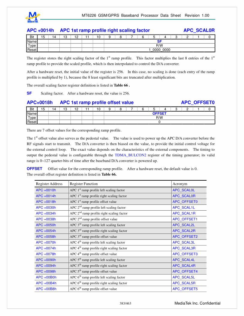
MT6226 GSM/GPRS Baseband Processor Data Sheet Revision 1.00
383/463 MediaTek Inc. Confidential
APC +0014h APC 1st ramp profile right scaling factor APC_SCAL0R Bit 15 14 13 12 11 10 9 8 7 6 5 4 3 2 1 0
Name SF Type R/W Reset 1_0000_0000
The register stores the right scaling factor of the 1st ramp profile. This factor multiplies the last 8 entries of the 1st ramp profile to provide the scaled profile, which is then interpolated to control the D/A converter.
After a hardware reset, the initial value of the register is 256. In this case, no scaling is done (each entry of the ramp profile is multiplied by 1), because the 8 least significant bits are truncated after multiplication.
The overall scaling factor register definition is listed in Table 66 .
SF Scaling factor. After a hardware reset, the value is 256.
APC+0018h APC 1st ramp profile offset value APC_OFFSET0 Bit 15 14 13 12 11 10 9 8 7 6 5 4 3 2 1 0
Name OFFSET Type R/W Reset 0
There are 7 offset values for the corresponding ramp profile.
The 1st offset value also serves as the pedestal value. The value is used to power up the APC D/A converter before the RF signals start to transmit. The D/A converter is then biased on the value, to provide the initial control voltage for the external control loop. The exact value depends on the characteristics of the external components. The timing to output the pedestal value is configurable through the TDMA_BULCON2 register of the timing generator; its valid range is 0~127 quarter-bits of time after the baseband D/A converter is powered up.
OFFSET Offset value for the corresponding ramp profile. After a hardware reset, the default value is 0. The overall offset register definition is listed in Table 66.
Register Address Register Function Acronym
APC +0010h APC 1st ramp profile left scaling factor APC_SCAL0L
APC +0014h APC 1st ramp profile right scaling factor APC_SCAL0R
APC +0018h APC 1st ramp profile offset value APC_OFFSET0
APC +0030h APC 2nd ramp profile left scaling factor APC_SCAL1L
APC +0034h APC 2nd ramp profile right scaling factor APC_SCAL1R
APC +0038h APC 2nd ramp profile offset value APC_OFFSET1
APC +0050h APC 3rd ramp profile left scaling factor APC_SCAL2L
APC +0054h APC 3rd ramp profile right scaling factor APC_SCAL2R
APC +0058h APC 3rd ramp profile offset value APC_OFFSET2
APC +0070h APC 4th ramp profile left scaling factor APC_SCAL3L
APC +0074h APC 4th ramp profile right scaling factor APC_SCAL3R
APC +0078h APC 4th ramp profile offset value APC_OFFSET3
APC +0090h APC 5th ramp profile left scaling factor APC_SCAL4L
APC +0094h APC 5th ramp profile right scaling factor APC_SCAL4R
APC +0098h APC 5th ramp profile offset value APC_OFFSET4
APC +00B0h APC 6th ramp profile left scaling factor APC_SCAL5L
APC +00B4h APC 6th ramp profile right scaling factor APC_SCAL5R
APC +00B8h APC 6th ramp profile offset value APC_OFFSET5

MT6226 GSM/GPRS Baseband Processor Data Sheet Revision 1.00
384/463 MediaTek Inc. Confidential
APC +00D0h APC 7th ramp profile left scaling factor APC_SCAL6L
APC +00D4h APC 7th ramp profile right scaling factor APC_SCAL6R
APC +00D8h APC 7th ramp profile offset value APC_OFFSET6
Table 66 APC scaling factor and offset value registers
APC+00E0h APC control register APC_CON Bit 15 14 13 12 11 10 9 8 7 6 5 4 3 2 1 0
Name GSM FPU Type R/W R/W Reset 1 0
GSM Defines the operation mode of the APC module. In GSM mode, each frame has only one slot, thus only one
scaling factor and one offset value must be configured. If the GSM bit is set, the programmer needs only to configure APC_SCAL0L and APC_OFFSET0. If the bit is not set, the APC module is operating in GPRS mode. 0 The APC module is operating in GPRS mode. 1 The APC module is operating in GSM mode. Default value.
FPU Forces the APC D/A converter to power up. Test only. 0 The APC D/A converter is not forced to power up. The converter is only powered on when the
transmission window is opened. Default value. 1 The APC D/A converter is forced to power up.
8.3.3 Ramp Profile Programming The first value of the first normalized ramp profile must be written in the least significant byte of the APC_PFA0 register. The second value must be written in the second least significant byte of the APC_PFA0, and so on.
Each ramp profile can be programmed to form an arbitrary shape.
The start of ramping is triggered by one of the TDMA_APCSTR signals. The timing relationship between TDMA_APCSTR and TDMA slots is depicted in Figure 140 for 4 consecutive time slots case. The power ramping profile must comply with the timing mask defined in GSM SPEC 05.05. The timing offset values for 7 ramp profiles are stored in the TDMA timer register from TDMA_APC0 to TDMA_APC6.
RX MXTX RX
TXTX TX
Figure 140 Timing diagram of TDMA_APCSTR.
Because the APC unit provides more than 5 ramp profiles, up to 4 consecutive transmission slots can accommodated. The 2 additional ramp profiles are useful particularly when the timing between the last 2 transmission time slots and CTIRQ is uncertain; software can begin writing the ramp profiles for the succeeding frame during the current frame, alleviating the risk of not writing the succeeding frame’s profile data in time.
In GPRS mode, to fit the intermediate ramp profile between different power levels, a simple scaling scheme is used to synthesize the ramp profile. The equation is as follows:

MT6226 GSM/GPRS Baseband Processor Data Sheet Revision 1.00
385/463 MediaTek Inc. Confidential
8 15 if 1,0 8 if 0,
0,1,...,15,DNSOFFDA
,...,151 ,2
DN DNS OFFDA
2
DN DNS OFFDA
12
12
0,1500
≥≥≥>
=
=⋅+=
=+⋅+=
+⋅+=
+
−
kk
l
k
k
klk
kklk
pre
where DA = the data to present to the D/A converter, DN = the normalized data which is stored in the register APC_PFn, S0 = the left scaling factor stored in register APC_SCALnL, S1 = the right scaling factor stored in register APC_SCALnR, and OFF = the offset value stored in the register APC_OFFSETn.
The subscript n denotes the index of the ramp profile.
The ramp calculation before interpolation is as depicted in Figure 141.
During each ramp process, each word of the normalized profile is first multiplied by 10-bit scaling factors and added to an offset value to form a bank of 18-bit words. The first 8 words (in the left half part as in Figure 141) are multiplied by the left scaling factor S0 and the last 8 words (in the right half part as in Figure 141) are multiplied by the right scaling factor S1. The lowest 8 bits of each word are then truncated to get a 10-bit result. The scaling factor is 0x100, which represents no scaling on reset. A value smaller than 0x100 scales the ramp profile down, and a value larger than 100 scales the ramp profile up.
DN0 * S0 + OFF
DN4 * S0 + OFF
DN8 * S1 + OFF
DN12 * S1 + OFFDN15 * S1 + OFF
16 Qb
DN4 * S0 DN8 * S1
OFF
Figure 141 The timing diagram of the APC ramp.
The 16 10-bit words are linearly interpolated into 32 10-bit words. A 10-bit D/A converter is then used to convert these 32 ramp values at a rate of 1.0833 MHz, that is, at quarter-bit rate. The timing diagram is shown in Figure 142 and the final value is retained on the output until the next event occurs.

MT6226 GSM/GPRS Baseband Processor Data Sheet Revision 1.00
386/463 MediaTek Inc. Confidential
TX TX
TX Burst TX Burst
TDMA_APCSTR0
Ramp ProfileRamp Profile Ramp Profile
TDMA_APCSTR2TDMA_APCSTR1
~29.5us ~29.5us
APC_DATA
TDMA_APCSTR1
TDMA_APCEN
TDMA_APCSTRx
~29.5us
offset
Figure 142 Timing diagram of the APC ramping.
The APC unit is only powered up when the APC window is open. The APC window is controlled by configuring the TDMA registers TDMA_BULCON1 and TDMA_BULCON2. Please refer to the TDMA timer unit for more detailed information.
The first offset value stored in the register APC_OFFSET0 also serves as the pedestal value, which is used to provide the initial power level for the PA.
Since the profile is not double-buffered, the timing to write the ramping profile is critical. The programmer must be restricted from writing to the data buffer during the ramping process, otherwise the ramp profile may be incorrect and lead to a malfunction.
8.4 Automatic Frequency Control (AFC) Unit
8.4.1 General description The Automatic Frequency Control (AFC) unit provides the direct control of the oscillator for frequency offset and Doppler shift compensation. The block diagram is of the AFC unit depicted in Figure 152. The module utilizes a 13-bit D/A converter to achieve high-resolution control. Two modes of operation provide flexibility when controlling the oscillator; they are described as follows.

MT6226 GSM/GPRS Baseband Processor Data Sheet Revision 1.00
387/463 MediaTek Inc. Confidential
;
+> ==:
:
:
APBBUS
TDMA_AFC( from TDMA timer )
-:
+> ==:
AFC_BUS
:
: :
TDMA_EVTVAL( from TDMA timer )
:
PDN_AFC( from global control )
VC
AFC unit
6 9 :
A > >
+> ==:
PDN_DACF_MODE
I_MODE
AFC
H_MODE HOLDN_DAC
Figure 152 The block diagram of the AFC controller
In timer-triggered mode, the TDMA timer controls the AFC enabling events. Each TDMA frame can pulse at most four events. Double buffer architecture is supported. AFC values can be written to the write buffers. When the signal TDMA_EVTVAL is received, the values in the write buffers are latched into the active buffers. However, AFC values can also be written to the active buffers directly. Each event is associated with an active buffer sharing the same index. When a TDMA event is triggered by TDMA_AFC, the value in the corresponding active buffer takes effect. Figure 153 shows a timing diagram of AFC events with respect to TX/RX/MX windows. In this mode, the D/A converter can stay powered on or be powered on for a programmable duration (256 quarter-bits, by default). The latter option is for power saving.
RX MX MXTX
AFC_STR0 AFC_STR3AFC_STR2AFC_STR1
Figure 153 Timing Diagram for the AFC Controller
In immediate mode, the MCU can directly control the AFC value without event-triggering. The value written by the MCU takes effect immediately. In this mode, the D/A converter must be powered on continuously. When transitioning from immediate mode into timer-triggered mode (by setting flag I_MODE in the register AFC_CON to be 0), the D/A converter is kept powered on for a programmable duration (256 quarter-bits by default) if a TDMA_AFC is not been pulsed. The duration is prolonged upon receiving events.
8.4.2 Register Definitions
AFC+0000h AFC control register AFC_CON Bit 15 14 13 12 11 10 9 8 7 6 5 4 3 2 1 0
Name H_MODE
RDACT
F_MODE
FETENV
I_MODE
Type R/w R/W R/W R/W R/W Reset 0 0 0 0 0
Four control modes are defined and can be controlled through the AFC control register. F_MODE enables the force power up mode. FETENV enables the direct write operation to the active buffer. I_MODE enables the immediate mode. RDACT enables the direct read operation from the active buffer. HOLD_ON enables the AFC DAC hold mode.
RDACT The flag enables the direct read operation from the active buffer. Note the control flag is only applicable to the four data buffer including AFC_DAT0, AFC_DAT1, AFC_DAT2, and AFC_DAT3. 0 APB read from the write buffer.

MT6226 GSM/GPRS Baseband Processor Data Sheet Revision 1.00
388/463 MediaTek Inc. Confidential
1 APB read from the active buffer. FETENV The flag enables the direct write operation to the active buffer. Note the control flag is only applicable to
the for data buffer including AFC_DAT0, AFC_DAT1, AFC_DAT2, and AFC_DAT3. 0 APB write to the write buffer. 1 APB write to the active buffer.
F_MODE The flag enables the force power up mode. 0 The force power up mode is not enabled. 1 The force power up mode is enabled.
I_MODE The flag enables the immediate mode. To enable the immediate mode also enable the force power up mode. 0 The immediate mode is not enabled. 1 The immediate mode is enabled.
H_MODE The flag enables the hold mode of AFC DAC. If this mode is enabled, the DAC will keep the previous voltage level instead of power down. 0 The hold mode is not enabled. 1 The hold mode is enabled.
AFC +0004h AFC data register 0 AFC_DAT0 Bit 15 14 13 12 11 10 9 8 7 6 15 4 3 2 1 0
Name AFCD Type R/W
The register stores the AFC value for the event 0 triggered by the TDMA timer in timer-triggered mode. When the RDACT or FETENV bit (of the AFC_CON register) is set, the data transfer operates on the active buffer. When neither flag is set, the data transfer operates on the write buffer.
AFCD The AFC sample for the D/A converter. Four registers (AFC_DAT0, AFC_DAT1, AFC_DAT2, AFC_DAT3) of the same type correspond to the event triggered by the TDMA timer. The four registers are summarized in Table 1.
Register Address Register Function Acronym
AFC +0004h AFC control value 0 AFC_DAT0
AFC +0008h AFC control value 1 AFC_DAT1
AFC +000Ch AFC control value 2 AFC_DAT2
AFC +0010h AFC control value 3 AFC_DAT3
Table 1 AFC Data Registers
Immediate mode can only use AFC_DAT0. In this mode, only the control value in the AFC_DAT0 write buffer is used to control the D/A converter. Unlike timer-triggered mode, the control value in AFC_DAT0 write buffer can bypass the active buffer stage and be directly coupled to the output buffer in immediate mode. To use immediate mode, program the AFC_DAT0 in advance and then enable immediate mode by setting the I_MODE flag in the AFC_CON register.
The registers AFC_DATA0, AFC_DAT1, AFC_DAT2, and AFC_DAT3 have no initial values, thus the register must be programmed before any AFC event takes place. The AFC value for the D/A converter, i.e., the output buffer value, is initially 0 after power up before any event occurs.
AFC +0014h AFC power up period AFC_PUPER Bit 15 14 13 12 11 10 9 8 7 6 5 4 3 2 1 0
Name PU_PER

MT6226 GSM/GPRS Baseband Processor Data Sheet Revision 1.00
389/463 MediaTek Inc. Confidential
Type R/W Reset ff
This register stores the AFC power up period, which is 13 bits wide. The value ranges from 0 to 8191. If the I_MODE or F_MODE flag is set, this register has no effect since the D/A converter is powered up continuously. If neither flag is set, the register controls the power up duration of the D/A converter. During that period, the signal PDN_DAC in Figure 152 is set to 1(power up).
PU_PER Stores the AFC power up period. After hardware power up, the field is initialized to 255.

MT6226 GSM/GPRS Baseband Processor Data Sheet Revision 1.00
390/463 MediaTek Inc. Confidential
9 Baseband Front End
Baseband Front End is a modem interface between TX/RX mixed-signal modules and digital signal processor (DSP). We can divide this block into two parts (see Figure 155). The first is the uplink (transmitting) path, which converts bit-stream from DSP into digital in-phase (I) and quadrature (Q) signals for TX mixed-signal module. The second part is the downlink (receiving) path, which receives digital in-phase (I) and quadrature (Q) signals from RX mixed-signal module, performs FIR filtering and then sends results to DSP. Figure 155 illustrates interconnection around Baseband Front End. In the figure the shadowed blocks compose Baseband Front End. The uplink path is mainly composed of GMSK Modulator and uplink parts of Baseband Serial Ports, and the downlink path is mainly composed of RX digital FIR filter and downlink parts of Baseband Serial Ports. Baseband Serial Ports is a serial interface used to communicate with DSP. In addition, there is a set of control registers in Baseband Front End that is intended for control of TX/RX mixed-signal modules, inclusive of calibration of DC offset and gain mismatch of downlink analog-to-digital (A/D) converters as well as uplink digital-to-analog (D/A) converters in TX/RX mixed-signal modules. The timing of bit streaming through Baseband Front End is completely under control of TDMA timer. Usually only either of uplink and downlink paths is active at one moment. However, both of the uplink and downlink paths will be active simultaneously when Baseband Front End is in loopback mode.
When either of TX windows in TDMA timer is opened, the uplink path in Baseband Front End will be activated. Accordingly components on the uplink path such as GMSK Modulator will be powered on, and then TX mixed-signal module is also powered on. The subblock Baseband Serial Ports will sink TX data bits from DSP and then forward them to GMSK Modulator. The outputs from GMSK Modulator are sent to TX mixed-signal module in format of I/Q signals. Finally D/A conversions are performed in TX mixed-signal module and the output analog signal is output to RF module.
Similarly, while either of RX windows in TDMA timer is opened, the downlink path in Baseband Front End will be activated. Accordingly components on the downlink path such as RX mixed-signal module and RX digital FIR filter are then powered on. First A/D conversions are performed in RX mixed-signal module, and then the results in format of I/Q signals are sourced to RX digital FIR filter. Low-Pass filtering is performed in RX digital FIR filter. Finally the results will be sourced to DSP through Baseband Serial Ports.
! " #
$% "#
Figure 155 Block Diagram Of Baseband Front End

MT6226 GSM/GPRS Baseband Processor Data Sheet Revision 1.00
391/463 MediaTek Inc. Confidential
9.1 Baseband Serial Ports
9.1.1 General Description Baseband Front End communicates with DSP through the sub block of Baseband Serial Ports. Baseband Serial Ports interfaces with DSP in serial manner. It implies that DSP must be configured carefully in order to have Baseband Serial Ports cooperate with DSP core correctly.
If downlink path is programmed in bypass-filter mode (NOT bypass-filter loopback mode), behavior of Baseband Serial Ports will completely be different from that in normal function mode. The special mode is for testing purpose. Please see the subsequent section of Downlink Path for details.
TX and RX windows are under control of TDMA timer. Please refer to functional specification of TDMA timer for the details how to open/close a TX/RX window. Opening/Closing of TX/RX windows has two major effects on Baseband Front End. They are power on/off of corresponding components and data souring/sinking. It is worth noticing that Baseband Serial Ports is only intended for sinking TX data from DSP or sourcing data to DSP. It does not involve power on/off of TX/RX mixed-signal modules.
As far as downlink path is concerned, if a RX window is opened by TDMA timer Baseband Front End will have RX mixed-signal module proceed to make A/D conversion, RX digital filter proceed to perform filtering and Baseband Serial Ports be activated to source data from RX digital filter to DSP no matter the data is meaningful or not. However, the interval between the moment that RX mixed-signal module is powered on and the moment that data proceed to be dumped by Baseband Serial Ports can be well controlled in TDMA timer. Lets denote as RX enable window the interval that RX mixed-signal module is powered on and denote as RX dump window the interval that data is dumped by Baseband Serial Ports. If the first samples from RX digital filter desire to be discarded, the corresponding RX enable window must cover the corresponding RX dump window. Notes that RX dump windows always win over RX enable windows. It means that a RX dump window will always raise a RX enable window. RX enable windows can be raised by TDMA timer or by programming RX power-down bit in global control registers to be ‘0’. It is useful in debugging environment.
Similarly, a TX dump window refers to the interval that Baseband Serial Ports sinks data from DSP on uplink path and a TX enable window refers to the interval that TX mixed-signal module is powered on. A TX window controlled by TDMA timer involves a TX dump window and a TX enable window simultaneously. The interval between the moment that TX mixed-signal module is powered on and the moment that data proceed to be forwarded from DSP to GMSK modulator by Baseband Serial Ports can be well controlled in TDMA timer. TX dump windows always win over TX enable windows. It means that a TX dump window will always raise a TX enable window. TX enable windows can be raised by TDMA timer or by programming TX power-down bit in global control registers to be ‘0’. It is useful in debugging environment.
Accordingly, Baseband Serial Ports are only under control of TX/RX dump window. Note that if TX/RX dump window is not integer multiplies of bit-time it will be extended to be integer multiplies of bit-time. For example, if TX/RX dump window has interval of 156.25 bit-times then it will be extended as 157 bit-times in Baseband Serial Ports.
9.1.2 Register Definitions
BFE+0000h Base-band Common Control Register BFE_CON Bit 15 14 13 12 11 10 9 8 7 6 5 4 3 2 1 0
Name BCIEN
Type R/W Reset 0

MT6226 GSM/GPRS Baseband Processor Data Sheet Revision 1.00
392/463 MediaTek Inc. Confidential
This register is for common control of Baseband Front End. It consists of ciphering encryption control.
BCIEN The bit is for ciphering encryption control. If the bit is set to ‘1’, XOR will performed on some TX bits (payload of Normal Burst) and ciphering pattern bit from DSP, and then the result is forwarded to GMSK Modulator. Meanwhile, Baseband Front End will generate signals to drive DSP ciphering process produce corresponding ciphering pattern bits if the bit is set to ‘1’. If the bit is set to ‘0’, the TX bit from DSP will be forwarded to GMSK modulator directly. Baseband Front End will not activate DSP ciphering process. 0 Disable ciphering encryption. 1 Enable ciphering encryption.
BFE +0004h Base-band Common Status Register BFE_STA Bit 15 14 13 12 11 10 9 8 7 6 5 4 3 2 1 0
Name BULFS
BULEN
BDLFS
BDLEN
Type RO RO RO RO Reset 0 0 0 0
This register indicates status of Baseband Front End. Under control of TDMA timer, Baseband Front End can be driven in several statuses. If downlink path is enabled, then the bit BDLEN will be ‘1’. Otherwise the bit BDLEN will be ‘0’. If downlink parts of Baseband Serial Ports is enabled, the bit BDLFS will be ‘1’. Otherwise the bit BDLFS will be ‘0’. If uplink path is enabled, then the bit BULEN will be ‘1’. Otherwise the bit BULEN will be 0. If uplink parts of Baseband Serial Ports is enabled, the bit BULFS will be ‘1’. Otherwise the bit BULFS will be ‘0’. Once downlink path is enabled, RX mixed-signal module will also be powered on. Similarly, once uplink path is enabled, TX mixed-signal module will also be powered on. Furthermore, enabling Baseband Serial Ports for downlink path refers to dumping results from RX digital FIR filter to DSP. Similarly, enabling Baseband Serial Ports for uplink path refers to forwarding TX bit from DSP to GMSK modulator. BDLEN stands for “Baseband DownLink ENable”. BULEN stands for “Baseband UpLink ENable”. BDLFS stands for “Baseband DownLink FrameSync”. BULFS stands for “Baseband UpLink FrameSync”.
BDLEN Indicate if downlink path is enabled. 0 Disabled 1 Enabled
BDLFS Indicate if Baseband Serial Ports for downlink path is enabled. 0 Disabled 1 Enabled
BULEN Indicate if uplink path is enabled. 0 Disabled 1 Enabled
BULFS Indicate if Baseband Serial Ports for uplink path is enabled. 0 Disabled 1 Enabled
9.2 Downlink Path (RX Path)
9.2.1 General Description On downlink path, the subblock between RX mixed-signal module and Baseband Serial Ports is RX Path. It mainly consists of a digital FIR filter, two sets of multiplexing paths for loopback modes, interface for RX mixed-signal module and interface for Baseband Serial Ports. The block diagram is shown in Figure 156.

MT6226 GSM/GPRS Baseband Processor Data Sheet Revision 1.00
393/463 MediaTek Inc. Confidential
While RX enable windows are opened, RX Path will issue control signals to have RX mixed-signal module proceed to make A/D conversion. As each conversion is finished, one set of I/Q signals will be latched. There exists a digital FIR filter for these I/Q signals. The result of filtering will be dumped to Baseband Serial Ports whenever RX dump windows are opened.
In addition to normal function, there are two loopback modes in RX Path. One is bypass-filter loopback mode, and the other is through-filter loopback mode. They are intended for verification of DSP firmware and hardware. The bypass-filter loopback mode refers to that RX digital FIR filter is not on the loopback path. However, the through-filter loopback mode refers to that RX digital FIR filter is on the loopback path.
The I/Q swap functionality is used to swap I/Q channel signals from RX mixed-signal module before they are latched into RX digital FIR filter. It is intended to provide flexibility for I/Q connection with RF modules.
There is a special data path not shown in Figure 156. It is a data path from RX mixed-signal module to Baseband Serial Ports. If downlink path is programmed in “Bypass RX digital FIR filter” mode, ADC outputs out of RX mixed-signal module will be directed into Baseband Serial Ports directly. Therefore these data can be dumped into DSP and RX FIR filtering will not be performed on them. Limited by bandwidth of the serial interface between Baseband Serial Ports and DSP, only ADC outputs which are from either I-channel or Q-channel ADC can be dumped into DSP. Both of I- and Q-channel ADC outputs cannot be dumped simultaneously. Which channel will be dumped is controlled by the register bit SWAP of the register RX_CFG when downlink path is programmed in “Bypass RX digital FIR filter” mode. See register definition below for details. The mode is for measurement of performance of A/D converters in RX mixed-signal module.
&%'"(
' (
)
&%'"(
' (
) *'#
!#
+ '',,'
*!%
-
$
,'!#
.#
.#
. (
,'
!#
.#
.#
.#
.#
.#
.#
.#
.#
.#
.#
.#
.#
Figure 156 Block Diagram Of RX Path
9.2.2 Register Definitions
BFE +0010h RX Configuration Register RX_CFG Bit 15 14 13 12 11 10 9 8 7 6 5 4 3 2 1 0

MT6226 GSM/GPRS Baseband Processor Data Sheet Revision 1.00
394/463 MediaTek Inc. Confidential
Name LPDN BYPFLTR
SWAP
Type R/W R/W R/W Reset 0000 0 0
This register is for configuration of downlink path, inclusive of configuration of RX mixed-signal module and RX path in Baseband Front End.
SWAP The register bit is for control of whether I/Q channel signals need swap before they are input to Baseband Front End. It provides flexibility of connection of I/Q channel signals between RF module and baseband module. The register bit has another purpose when the register bit “BYPFLTR” is set to 1. Please see description for the register bit “BYPFLTR”. 0 I- and Q-channel signals are not swapped 1 I- and Q-channel signals are swapped
BYPFLTR Bypass RX FIR filter control. The register bit is used to configure Baseband Front End in the state called “Bypass RX FIR filter state” or not. Once the bit is set to ‘1’, RX FIR filter will be bypassed. That is, ADC outputs of RX mixed-signal module that are 11-bit resolution and at sampling rate of 1.083MHz can be dumped into DSP by Baseband Serial Ports and RX FIR filtering will not be performed on them. Limited by bandwidth of the serial interface between Baseband Serial Ports and DSP, these ADC outputs are all from either I-channel or Q-channel ADC. Both of I- and Q-channel ADC outputs cannot be dumped simultaneously. When the bit is set to ‘1’ and the register bit “SWAP” is set to ‘0’, ADC outputs of I-channel will be dumped. When the bit is set to ‘1’ and the register bit “SWAP” is set to ‘1’, ADC outputs of Q-channel will be dumped. 0 Not bypass RX FIR filter
1 Bypass RX FIR filter LPDN Late power down control. RX mixed-signal module needs two power down signals. There must exist some
delay between them. The register field is used to control the late-arriving power-down signal. 0000 The delay between two power-down signals is one 13 MHz period. 0001 The delay between two power-down signals is two 13 MHz period. 0010 The delay between two power-down signals is three 13 MHz period. … 0001 The delay between two power-down signals is 256 13 MHz period.
BFE +0014h RX Control Register RX_CON Bit 15 14 13 12 11 10 9 8 7 6 5 4 3 2 1 0
Name BLPEN[1:0] Type R/W Reset 0
This register is for control of downlink path, inclusive of control of RX mixed-signal module and RX path in Baseband Front End module.
BLPEN The register field is for loopback configuration selection in Baseband Front End. 00 Configure Baseband Front End in normal function mode 01 Configure Baseband Front End in bypass-filter loopback mode 10 Configure Baseband Front End in through-filter loopback mode 11 Reserved
BFE +0020h RX Digital FIR Filter Coefficient Register 0 RX_FIR_COEF0 Bit 15 14 13 12 11 10 9 8 7 6 5 4 3 2 1 0
Name D9 D8 D7 D6 D5 D4 D3 D2 D1 D0 Type R/W R/W R/W R/W R/W R/W R/W R/W R/W R/W Reset 0 0 0 0 0 0 0 0 0 0

MT6226 GSM/GPRS Baseband Processor Data Sheet Revision 1.00
395/463 MediaTek Inc. Confidential
The register is for RX digital FIR filter coefficient 0. It is coded in 2’s complement. That is, its maximum is 255 and its minimum is –256. It will be applied on the latest and the oldest taps of 31 taps. The equivalent process flow of RX digital FIR filtering is shown in Figure 157.
/
0
',/
',
',0
1
2
3
',1
4
5
06
07
1/
',2
',3
',2
',1
',/
',
',0
,
#,!# !
' 8 89
-!.
'
Figure 157 Equivalent Process Flow Of RX Digital FIR Filtering
BFE +0024h RX Digital FIR Filter Coefficient Register 1 RX_FIR_COEF1 Bit 15 14 13 12 11 10 9 8 7 6 5 4 3 2 1 0
Name D9 D8 D7 D6 D5 D4 D3 D2 D1 D0 Type R/W R/W R/W R/W R/W R/W R/W R/W R/W R/W Reset 0 0 0 0 0 0 0 0 0 0
The register is for RX digital FIR filter coefficient 1. It is coded in 2’s complement. That is, its maximum is 255 and its minimum is –256.
BFE +0028h RX Digital FIR Filter Coefficient Register 2 RX_FIR_COEF2 Bit 15 14 13 12 11 10 9 8 7 6 5 4 3 2 1 0
Name D9 D8 D7 D6 D5 D4 D3 D2 D1 D0 Type R/W R/W R/W R/W R/W R/W R/W R/W R/W R/W

MT6226 GSM/GPRS Baseband Processor Data Sheet Revision 1.00
396/463 MediaTek Inc. Confidential
Reset 0 0 0 0 0 0 0 0 0 0
The register is for RX digital FIR filter coefficient 2. It is coded in 2’s complement. That is, its maximum is 255 and its minimum is –256.
BFE +002Ch RX Digital FIR Filter Coefficient Register 3 RX_FIR_COEF3 Bit 15 14 13 12 11 10 9 8 7 6 5 4 3 2 1 0
Name D9 D8 D7 D6 D5 D4 D3 D2 D1 D0 Type R/W R/W R/W R/W R/W R/W R/W R/W R/W R/W Reset 0 0 0 0 0 0 0 0 0 0
The register is for RX digital FIR filter coefficient 3. It is coded in 2’s complement. That is, its maximum is 255 and its minimum is –256.
BFE +0030h RX Digital FIR Filter Coefficient Register 4 RX_FIR_COEF4 Bit 15 14 13 12 11 10 9 8 7 6 5 4 3 2 1 0
Name D9 D8 D7 D6 D5 D4 D3 D2 D1 D0 Type R/W R/W R/W R/W R/W R/W R/W R/W R/W R/W Reset 0 0 0 0 0 0 0 0 0 0
The register is for RX FIR filter coefficient 4. It is coded in 2’s complement. That is, its maximum is 255 and its minimum is –256.
BFE +0034h RX Digital FIR Filter Coefficient Register 5 RX_FIR_COEF5 Bit 15 14 13 12 11 10 9 8 7 6 5 4 3 2 1 0
Name D9 D8 D7 D6 D5 D4 D3 D2 D1 D0 Type R/W R/W R/W R/W R/W R/W R/W R/W R/W R/W Reset 0 0 0 0 0 0 0 0 0 0
The register is for RX digital FIR filter coefficient 5. It is coded in 2’s complement. That is, its maximum is 255 and its minimum is –256.
BFE +0038h RX Digital FIR Filter Coefficient Register 6 RX_FIR_COEF6 Bit 15 14 13 12 11 10 9 8 7 6 5 4 3 2 1 0
Name D9 D8 D7 D6 D5 D4 D3 D2 D1 D0 Type R/W R/W R/W R/W R/W R/W R/W R/W R/W R/W Reset 0 0 0 0 0 0 0 0 0 0
The register is for RX digital FIR filter coefficient 6. It is coded in 2’s complement. That is, its maximum is 255 and its minimum is –256.
BFE +003Ch RX Digital FIR Filter Coefficient Register 7 RX_FIR_COEF7 Bit 15 14 13 12 11 10 9 8 7 6 5 4 3 2 1 0
Name D9 D8 D7 D6 D5 D4 D3 D2 D1 D0 Type R/W R/W R/W R/W R/W R/W R/W R/W R/W R/W Reset 0 0 0 0 0 0 0 0 0 0
The register is for RX digital FIR filter coefficient 7. It is coded in 2’s complement. That is, its maximum is 255 and its minimum is –256.
BFE +0040h RX Digital FIR Filter Coefficient Register 8 RX_FIR_COEF8 Bit 15 14 13 12 11 10 9 8 7 6 5 4 3 2 1 0
Name D9 D8 D7 D6 D5 D4 D3 D2 D1 D0 Type R/W R/W R/W R/W R/W R/W R/W R/W R/W R/W Reset 0 0 0 0 0 0 0 0 0 0

MT6226 GSM/GPRS Baseband Processor Data Sheet Revision 1.00
397/463 MediaTek Inc. Confidential
The register is for RX digital FIR filter coefficient 8. It is coded in 2’s complement. That is, its maximum is 255 and its minimum is –256.
BFE +0044h RX Digital FIR Filter Coefficient Register 9 RX_FIR_COEF9 Bit 15 14 13 12 11 10 9 8 7 6 5 4 3 2 1 0
Name D9 D8 D7 D6 D5 D4 D3 D2 D1 D0 Type R/W R/W R/W R/W R/W R/W R/W R/W R/W R/W Reset 0 0 0 0 0 0 0 0 0 0
The register is for RX digital FIR filter coefficient 9. It is coded in 2’s complement. That is, its maximum is 255 and its minimum is –256.
BFE +0048h RX Digital FIR Filter Coefficient Register 10 RX_FIR_COEF1
0 Bit 15 14 13 12 11 10 9 8 7 6 5 4 3 2 1 0
Name D9 D8 D7 D6 D5 D4 D3 D2 D1 D0 Type R/W R/W R/W R/W R/W R/W R/W R/W R/W R/W Reset 0 0 0 0 0 0 0 0 0 0
The register is for RX digital FIR filter coefficient 10. It is coded in 2’s complement. That is, its maximum is 255 and its minimum is –256.
BFE +004Ch RX Digital FIR Filter Coefficient Register 11 RX_FIR_COEF1
1 Bit 15 14 13 12 11 10 9 8 7 6 5 4 3 2 1 0
Name D9 D8 D7 D6 D5 D4 D3 D2 D1 D0 Type R/W R/W R/W R/W R/W R/W R/W R/W R/W R/W Reset 0 0 0 0 0 0 0 0 0 0
The register is for RX digital FIR filter coefficient 11. It is coded in 2’s complement. That is, its maximum is 255 and its minimum is –256.
BFE +0050h RX Digital FIR Filter Coefficient Register 12 RX_FIR_COEF1
2 Bit 15 14 13 12 11 10 9 8 7 6 5 4 3 2 1 0
Name D9 D8 D7 D6 D5 D4 D3 D2 D1 D0 Type R/W R/W R/W R/W R/W R/W R/W R/W R/W R/W Reset 0 0 0 0 0 0 0 0 0 0
The register is for RX digital FIR filter coefficient 12. It is coded in 2’s complement. That is, its maximum is 255 and its minimum is –256.
BFE +0054h RX Digital FIR Filter Coefficient Register 13 RX_FIR_COEF1
3 Bit 15 14 13 12 11 10 9 8 7 6 5 4 3 2 1 0
Name D9 D8 D7 D6 D5 D4 D3 D2 D1 D0 Type R/W R/W R/W R/W R/W R/W R/W R/W R/W R/W Reset 0 0 0 0 0 0 0 0 0 0
The register is for RX digital FIR filter coefficient 13. It is coded in 2’s complement. That is, its maximum is 255 and its minimum is –256.

MT6226 GSM/GPRS Baseband Processor Data Sheet Revision 1.00
398/463 MediaTek Inc. Confidential
BFE +0058h RX Digital FIR Filter Coefficient Register 14 RX_FIR_COEF1
4 Bit 15 14 13 12 11 10 9 8 7 6 5 4 3 2 1 0
Name D9 D8 D7 D6 D5 D4 D3 D2 D1 D0 Type R/W R/W R/W R/W R/W R/W R/W R/W R/W R/W Reset 0 0 0 0 0 0 0 0 0 0
The register is for RX digital FIR filter coefficient 14. It is coded in 2’s complement. That is, its maximum is 255 and its minimum is –256.
BFE +005Ch RX Digital FIR Filter Coefficient Register 15 RX_FIR_COEF1
5 Bit 15 14 13 12 11 10 9 8 7 6 5 4 3 2 1 0
Name D9 D8 D7 D6 D5 D4 D3 D2 D1 D0 Type R/W R/W R/W R/W R/W R/W R/W R/W R/W R/W Reset 0 0 0 0 0 0 0 0 0 0
The register is for RX digital FIR filter coefficient 15. It is coded in 2’s complement. That is, its maximum is 255 and its minimum is –256.
9.3 Uplink Path (TX Path)
9.3.1 General Description The purpose of the uplink path inside Baseband Front End is to sink TX symbols, one bit for each symbol, from DSP, then perform GMSK modulation on them, then perform offset cancellation on I/Q digital signals out of GMSK modulator, and finally control TX mixed-signal module to make D/A conversion on I/Q signals out of GMSK Modulator with offset cancellation. Accordingly, the uplink path is composed of uplink parts of Baseband Serial Ports, GSM Encryptor, GMSK Modulator and Offset Cancellation. The block diagram of uplink path is shown in Figure 158. On uplink path, the content of a burst, including tail bits, data bits, and training sequence bits is sent from DSP. Translated by GMSK Modulator, these bits will become I/Q digital signals. Offset cancellation will be performed on these I/Q digital signals to compensate offset error of D/A converters (DAC) in TX mixed-signal module. Finally the generated I/Q digital signals will be input to TX mixed-signal module that contains two DAC for I/Q signal respectively. The details of each subblock will be described in subsequent sections.
) '+%
$% "
:,
:,,
. '
+
+
* *
Figure 158 Block Diagram Of Uplink Path
TDMA timer having a quarter-bit timing accuracy gives the timing windows for uplink operation. Uplink operation is controlled by TX enable window and TX dump window of TDMA timer. Usually TX enable window is opened earlier than TX dump window. When TX enable window of TDMA timer is opened, uplink path in Baseband Front End will

MT6226 GSM/GPRS Baseband Processor Data Sheet Revision 1.00
399/463 MediaTek Inc. Confidential
power on GSK TX mixed-signal module and thus has it drive valid outputs to RF module. However, uplink parts of Baseband Serial Ports still don’t sink data from DSP through the serial interface between Baseband Serial Ports and DSP until now. Uplink parts of Baseband Serial Ports will not sink data from DSP until TX dump window of TDMA timer is opened.
9.3.2 Register Definitions
BFE +0060h TX Configuration Register TX_CFG Bit 15 14 13 12 11 10 9 8 7 6 5 4 3 2 1 0
Name APNDEN
Type R/W Reset 0
This register is for configuration of uplink path, inclusive of configuration of TX mixed-signal module and TX path in Baseband Front End.
APNDEN Appending Bits Enable. The register bit is used to control the ending scheme of GMSK modulation. 0 Suitable for GPRS. If a TX enable window contains several TX dump window, then GMSK modulator
will still output in the intervals between two TX dump window and all 1’s will be fed into GMSK modulator. Note that when the bit is set to ‘0’, the interval between the moment at which TX enable window is activated and the moment at which TX dump window is activated must be multiples of one bit time.
1 Suitable for GSM only. After a TX dump window, GMSK modulator will only output for some bit time.
BFE +0064h TX Control Register TX_CON Bit 15 14 13 12 11 10 9 8 7 6 5 4 3 2 1 0
Name IQSWP_MODSEL
CALRCEN
IQSWP
Type R/W R/W R/W Reset 0 0 0
This register is for control of uplink path, inclusive of control of TX mixed-signal module and TX path in Baseband Front End.
IQSWP_MODSEL The register bit is for control of I/Q swapping mode select to fit different RF application requirement. When the bit is set to ‘1’, IQSWP control register can be configured on the fly, while IQSWP control register will be only updated at rising edge of TDMA event Validate before each TDMA frame. 0: IQSWP control register can’t be configured on the fly 1: IQSWP control register can be configured on the fly.
CALRCEN Calibration for TX low-pass-filter Enable. The procedure to make calibration processing for smoothing filter in BBTX mixed-signal module is as follows:
1. Write ‘1’ to the register bit CARLC in the register TX_CON of Baseband Front End in order to activate clock required for calibration process. Initiate calibration process.
2. Write ‘1’ to the register bit STARTCALRC of Analog Chip Interface. Start calibration process.
3. Read the register bit CALRCDONE of Analog Chip Interface. If read as ‘1’, then calibration process finished. Otherwise repeat the step.
4. Write ‘0’ to the register bit STARTCALRC of Analog Chip Interface. Stop calibration process.

MT6226 GSM/GPRS Baseband Processor Data Sheet Revision 1.00
400/463 MediaTek Inc. Confidential
5. Write ‘0’ to the register bit CARLC in the register TX_CON of Baseband Front End in order to deactivate clock required for calibration process. Terminate calibration process.
6. The result of calibration process can be read from the register field CALRCOUT of the register BBTX_AC_CON1 of Analog Chip Interface. Software can set the value to the register field CALRCSEL for 3-dB cutoff frequency selection of smoothing filter in DAC of BBTX of Analog Chip Interface.
0 Deactivate clock required for calibration process. 1 Activate clock required for calibration process.
IQSWP The register bit is for control of I/Q swapping. When the bit is set to ‘1’, phase on I/Q plane will rotate in inverse direction. While IQSWAP_MODSEL set to one, double buffer architecture is supported. IQSWP values can be written to the write buffers. When the signal TDMA_EVTVAL is received, the values in the write buffers are latched into the active buffers. If IQSWAP_MODSEL set to zero, no double buffer feature will be turned on. 0: I and Q are not swapped. 1: I and Q are swapped.
BFE +0068h TX I/Q Channel Offset Compensation Register TX_OFF Bit 15 14 13 12 11 10 9 8 7 6 5 4 3 2 1 0
Name OFFQ[5:0] OFFI[5:0] Type R/W R/W Reset 000000 000000
The register is for offset cancellation of I-channel DAC in TX mixed-signal module. It is for compensation of offset error caused by I/Q-channel DAC in TX mixed-signal module. It is coded in 2’s complement, that is, with maximum 31 and minimum –32.
OFFI Value of offset cancellation for I-channel DAC in TX mixed-signal module OFFQ Value of offset cancellation for Q-channel DAC in TX mixed-signal module

MT6226 GSM/GPRS Baseband Processor Data Sheet Revision 1.00
401/463 MediaTek Inc. Confidential
10 Timing Generator
Timing is the most critical issue in GSM/GPRS applications. The TDMA timer provides a simple interface for the MCU to program all the timing-related events for receive event control, transmit event control and the timing adjustment. Detailed descriptions are mentioned in Section 10.1.
In pause mode, the 13MHz reference clock may be switched off temporarily for the purpose of power saving and the synchronization to the base-station is maintained by using a low power 32KHz crystal oscillator. The 32KHz oscillator is not accurate and therefore it should be calibrated prior to entering pause mode. The calibration sequence, pause begin sequence and the wake up sequence are described in Section 10.2.
10.1 TDMA timer The TDMA timer unit is composed of three major blocks: Quarter bit counter, Signal generator and Event registers.
Figure 159 The block diagram of TDMA timer
By default, the quarter-bit counter continuously counts from 0 to the wrap position. In order to apply to cell synchronization and neighboring cell monitoring, the wrap position can be changed by the MCU to shorten or lengthen a TDMA frame. The wrap position is held in the TDMA_WRAP register and the current value of the TDMA quarter bit counter may be read by the MCU via the TDMA_TQCNT register.
The signal generator handles the overall comparing and event-generating processes. When a match has occurred between the quarter bit counter and the event register, a predefined control signal is generated. These control signals may be used for on-chip and off-chip purposes. Signals that change state more than once per frame make use of more than one event register.
The event registers are programmed to contain the quarter bit position of the event that is to occurr. The event registers are double buffered. The MCU writes into the first register, and the event TDMA_EVTVAL transfers the data from the write buffer to the active buffer, which is used by the signal generator for comparison with the quarter bit count. The TDMA_EVTVAL signal itself may be programmed at any quarter bit position. These event registers could be classified into four groups:
On-chip Control Events
TDMA_EVTVAL This event allows the data values written by the MCU to pass through to the active buffers.
TDMA_WRAP

MT6226 GSM/GPRS Baseband Processor Data Sheet Revision 1.00
402/463 MediaTek Inc. Confidential
TDMA quarter bit counter wrap position. This sets the position at which the TDMA quarter bit counter resets back to zero. The default value is 4999, changing this value will advance or retard the timing events in the frame following the next TDMA_EVTVAL signal.
TDMA_DTIRQ DSP TDMA interrupt requests. DTIRQ triggers the DSP to read the command from the MCU/DSP Shard RAM to schedule the activities that will be executed in the current frame.
TDMA_CTIRQ1/CTIRQ2 MCU TDMA interrupt requests.
TDMA_AUXADC [1:0]
This signal triggers the monitoring ADC to measure the voltage, current, temperature, device id etc..
TDMA_AFC [3:0] This signal powers up the automatic frequency control DAC for a programmed duration after this event.
Note: For both MCU and DSP TDMA interrupt requests, these signals are all active Low during one quarter bit duration and they should be used as edge sensitive events by the respective interrupt controllers.
On-chip Receive Events
TDMA_BDLON [5:0] These registers are a set of six which contain the quarter bit event that initiates the receive window assertion sequence which powers up and enables the receive ADC, and then enables loading of the receive data into the receive buffer.
TDMA_BDLOFF [5:0] These registers are a set of six which contain the quarter bit event that initiates the receive window de-assertion sequence which disables loading of the receive data into the receive buffer, and then powers down the receive ADC.
TDMA_RXWIN[5:0] DSP TDMA interrupt requests. TDMA_RXWIN is usually used to initiate the related RX processing including two modes. In single-shot mode, TDMA_RXWIN is generated when the BRXFS signal is de-asserted. In repetitive mode, TDMA_RXWIN will be generated both regularly with a specific interval after BRXFS signal is asserted and when the BRXFS signal is de-asserted.
Figure 160 The timing diagram of BRXEN and BRXFS
Note: TDMA_BDLON/OFF event registers, together with TDMA_BDLCON register, generate the corresponding BRXEN and BRXFS window used to power up/down baseband downlink path and control the duration of data transmission to the DSP, respectively.
On-chip Transmit Events
TDMA_APC [6:0] These registers initiate the loading of the transmit burst shaping values from the transmit burst shaping RAM into the transmit power control DAC.
TDMA_BULON [3:0] This register contains the quarter bit event that initiates the transmit window assertion sequence which powers up the modulator DAC and then enables reading of bits from the transmit buffer into the GMSK modulator.
TDMA_BULOFF [3:0] This register contains the quarter bit event that initiates the transmit window de-assertion sequence which disables the reading of bits from the transmit buffer into the GMSK modulator, and then power down the modulator DAC.

MT6226 GSM/GPRS Baseband Processor Data Sheet Revision 1.00
403/463 MediaTek Inc. Confidential
Figure 161 The timing diagram of BTXEN and BTXFS
Note: TDMA_BULON/OFF event registers, together with TDMA_BULCON1, TDMA_BULCON2 register, generate the corresponding BTXEN, BTXFS and APCEN window used to power up/down the baseband uplink path, control the duration of data transmission from the DSP and power up/down the APC DAC, respectively. Off-chip Control Events
TDMA_BSI [15:0] The quarter bit positions of these 16 BSI events are used to initiate the transfer of serial words to the transceiver and synthesizer for gain control and frequency adjustment.
TDMA_BPI [25:0] The quarter bit positions of these 26 BPI events are used to generate changes of state on the output pins to control the external radio components.
10.1.1 Register Definitions
TDMA+0150h Event Enable Register 0 TDMA_EVTENA
0 Bit 15 14 13 12 11 10 9 8 7 6 5 4 3 2 1 0
Name AFC3 AFC2 AFC1 AFC0 BDL5 BDL4 BDL3 BDL2 BDL1 BDL0 CTIRQ2
CTIRQ1
DTIRQ
Type R/W R/W R/W R/W R/W R/W R/W R/W R/W R/W R/W R/W R/W Reset 0 0 0 0 0 0 0 0 0 0 0 0 0
DTIRQ Enable TDMA_DTIRQ CTIRQn Enable TDMA_CTIRQn AFCn Enable TDMA_AFCn BDLn Enable TDMA_BDLONn and TDMA_BDLOFFn For all these bits,
0 function is disabled 1 function is enabled
TDMA+0154h Event Enable Register 1 TDMA_EVTENA
1 Bit 15 14 13 12 11 10 9 8 7 6 5 4 3 2 1 0
Name GPRS BUL3 BUL2 BUL1 BUL0 APC6 APC5 APC4 APC3 APC2 APC1 APC0 Type R/W R/W R/W R/W R/W R/W R/W R/W R/W R/W R/W R/W Reset 0 0 0 0 0 0 0 0 0 0 0 0
APCn Enable TDMA_APCn BULn Enable TDMA_BULONn and TDMA_BULOFFn For all these bits,
0 function is disabled 1 function is enabled

MT6226 GSM/GPRS Baseband Processor Data Sheet Revision 1.00
404/463 MediaTek Inc. Confidential
TDMA +0158h Event Enable Register 2 TDMA_EVTENA
2 Bit 15 14 13 12 11 10 9 8 7 6 5 4 3 2 1 0
Name BSI15 BSI14 BSI13 BSI12 BSI11 BSI10 BSI9 BSI8 BSI7 BSI6 BSI5 BSI4 BSI3 BSI2 BSI1 BSI0 Type R/W R/W R/W R/W R/W R/W R/W R/W R/W R/W R/W R/W R/W R/W R/W R/W Reset 0 0 0 0 0 0 0 0 0 0 0 0 0 0 0 0
BSIn BSI event enable control
0 Disable TDMA_BSIn 1 Enable TDMA_BSIn
TDMA +015Ch Event Enable Register 3 TDMA_EVTENA
3 Bit 15 14 13 12 11 10 9 8 7 6 5 4 3 2 1 0
Name BPI15 BPI14 BPI13 BPI12 BPI11 BPI10 BPI9 BPI8 BPI7 BPI6 BPI5 BPI4 BPI3 BPI2 BPI1 BPI0 Type R/W R/W R/W R/W R/W R/W R/W R/W R/W R/W R/W R/W R/W R/W R/W R/W Reset 0 0 0 0 0 0 0 0 0 0 0 0 0 0 0 0
TDMA+0160h Event Enable Register 4 TDMA_EVTENA
4 Bit 15 14 13 12 11 10 9 8 7 6 5 4 3 2 1 0
Name BPI25 BPI24 BPI23 BPI22 BPI21 BPI20 BPI19 BPI18 BPI17 BPI16 Type R/W R/W R/W R/W R/W R/W R/W R/W R/W R/W Reset 0 0 0 0 0 0 0 0 0 0
BPIn BPI event enable control
0 Disable TDMA_BPIn 1 Enable TDMA_BPIn
TDMA+0164h Event Enable Register 5 TDMA_EVTENA
5 Bit 15 14 13 12 11 10 9 8 7 6 5 4 3 2 1 0
Name AUX1 AUX0 Type R/W R/W Reset 0 0
AUX Auxiliary ADC event enable control
0 Disable Auxiliary ADC event 1 Enable Auxiliary ADC event
TDMA +0170h Qbit Timer Offset Control Register TDMA_WRAPO
FS Bit 15 14 13 12 11 10 9 8 7 6 5 4 3 2 1 0
Name TOI[1:0] Type R/W Reset 0
TOI This register defines the value used to advance the Qbit timer in unit of 1/4 quarter bit; the timing advance will
be take place as soon as the TDMA_EVTVAL is occurred, and it will be cleared automatically.

MT6226 GSM/GPRS Baseband Processor Data Sheet Revision 1.00
405/463 MediaTek Inc. Confidential
TDMA +0174h Qbit Timer Biasing Control Register TDMA_REGBIA
S Bit 15 14 13 12 11 10 9 8 7 6 5 4 3 2 1 0
Name TQ_BIAS[13:0] Type R/W Reset 0
TQ_BIAS This register defines the Qbit offset value which will be added to the registers being programmed. It only
takes effects on AFC, BDLON/OFF, BULON/OFF, APC, AUXADC, BSI and BPI event registers.
TDMA +0180h DTX Control Register TDMA_DTXCON Bit 15 14 13 12 11 10 9 8 7 6 5 4 3 2 1 0
Name DTX3 DTX2 DTX1 DTX0 Type R/W R/W R/W R/W
DTX DTX flag is used to disable the associated transmit signals
0 BULON0, BULOFF0, APC_EV0 & APC_EV1 are controlled by TDMA_EVTENA1 register 1 BULON0, BULOFF0, APC_EV0 & APC_EV1 are disabled
TDMA +0184h Receive Interrupt Control Register TDMA_RXCON Bit 15 14 13 12 11 10 9 8 7 6 5 4 3 2 1 0
Name MOD5 MOD4 MOD3 MOD2 MOD1 MOD0 RXINTCNT[9:0] Type R/W R/W R/W R/W R/W R/W R/W
RXINTCNT TDMA_RXWIN interrupt generation interval in quarter bit unit MODn Mode of Receive Interrupts
0 Single shot mode for the corresponding receive window 1 Repetitive mode for the corresponding receive window
TDMA +0188h Baseband Downlink Control Register TDMA_BDLCO
N Bit 15 14 13 12 11 10 9 8 7 6 5 4 3 2 1 0
Name ADC_ON ADC_OFF Type R/W R/W
ADC_ON BRXEN to BRXFS setup up time in quarter bit unit. ADC_OFF BRXEN to BRXFS hold up time in quarter bit unit.
TDMA +018Ch Baseband Uplink Control Register 1 TDMA_BULCO
N1 Bit 15 14 13 12 11 10 9 8 7 6 5 4 3 2 1 0
Name DAC_ON DAC_OFF Type R/W R/W
DAC_ON BTXEN to BTXFS setup up time in quarter bit unit. DAC_OFF BTXEN to BTXFS hold up time in quarter bit unit.
TDMA +0190h Baseband Uplink Control Register 2 TDMA_BULCO
N2 Bit 15 14 13 12 11 10 9 8 7 6 5 4 3 2 1 0
Name APC_HYS Type R/W

MT6226 GSM/GPRS Baseband Processor Data Sheet Revision 1.00
406/463 MediaTek Inc. Confidential
APC_HYS APCEN to BTXEN hysteresis time in quarter bit unit.
Address Type Width Reset Value Name Description +0000h R [13:0] — TDMA_TQCNT Read quarter bit counter +0004h R/W [13:0] 0x1387 TDMA_WRAP Latched Qbit counter reset position +0008h R/W [13:0] 0x1387 TDMA_WRAPIMD Direct Qbit counter reset position +000Ch R/W [13:0] 0x0000 TDMA_EVTVAL Event latch position +0010h R/W [13:0] — TDMA_DTIRQ DSP software control +0014h R/W [13:0] — TDMA_CTIRQ1 MCU software control 1 +0018h R/W [13:0] — TDMA_CTIRQ2 MCU software control 2 +0020h R/W [13:0] — TDMA_AFC0 The 1st AFC control +0024h R/W [13:0] — TDMA_AFC1 The 2nd AFC control +0028h R/W [13:0] — TDMA_AFC2 The 3rd AFC control +002Ch R/W [13:0] — TDMA_AFC3 The 4th AFC control +0030h R/W [13:0] — TDMA_BDLON0 +0034h R/W [13:0] — TDMA_BDLOFF0
Data serialization of the 1st RX block
+0038h R/W [13:0] — TDMA_BDLON1 +003Ch R/W [13:0] — TDMA_BDLOFF1
Data serialization of the 2nd RX block
+0040h R/W [13:0] — TDMA_BDLON2 +0044h R/W [13:0] — TDMA_BDLOFF2
Data serialization of the 3rd RX block
+0048h R/W [13:0] — TDMA_BDLON3 +004Ch R/W [13:0] — TDMA_BDLOFF3
Data serialization of the 4th RX block
+0050h R/W [13:0] — TDMA_BDLON4 +0054h R/W [13:0] — TDMA_BDLOFF4
Data serialization of the 5th RX block
+0058h R/W [13:0] — TDMA_BDLON5 +005Ch R/W [13:0] — TDMA_BDLOFF5
Data serialization of the 6th RX block
+0060h R/W [13:0] — TDMA_BULON0 +0064h R/W [13:0] — TDMA_BULOFF0
Data serialization of the 1st TX slot
+0068h R/W [13:0] — TDMA_BULON1 +006Ch R/W [13:0] — TDMA_BULOFF1
Data serialization of the 2nd TX slot
+0070h R/W [13:0] — TDMA_BULON2 +0074h R/W [13:0] — TDMA_BULOFF2
Data serialization of the 3rd TX slot
+0078h R/W [13:0] — TDMA_BULON3 +007Ch R/W [13:0] — TDMA_BULOFF3
Data serialization of the 4th TX slot
+0090h R/W [13:0] — TDMA_APC0 The 1st APC control +0094h R/W [13:0] — TDMA_APC1 The 2nd APC control +0098h R/W [13:0] — TDMA_APC2 The 3rd APC control +009Ch R/W [13:0] — TDMA_APC3 The 4th APC control +00A0h R/W [13:0] — TDMA_APC4 The 5th APC control +00A4h R/W [13:0] — TDMA_APC5 The 6th APC control +00A8h R/W [13:0] — TDMA_APC6 The 7th APC control +00B0h R/W [13:0] — TDMA_BSI0 BSI event 0 +00B4h R/W [13:0] — TDMA_BSI1 BSI event 1 +00B8h R/W [13:0] — TDMA_BSI2 BSI event 2 +00BCh R/W [13:0] — TDMA_BSI3 BSI event 3 +00C0h R/W [13:0] — TDMA_BSI4 BSI event 4 +00C4h R/W [13:0] — TDMA_BSI5 BSI event 5 +00C8h R/W [13:0] — TDMA_BSI6 BSI event 6 +00CCh R/W [13:0] — TDMA_BSI7 BSI event 7 +00D0h R/W [13:0] — TDMA_BSI8 BSI event 8 +00D4h R/W [13:0] — TDMA_BSI9 BSI event 9 +00D8h R/W [13:0] — TDMA_BSI10 BSI event 10 +00DCh R/W [13:0] — TDMA_BSI11 BSI event 11 +00E0h R/W [13:0] — TDMA_BSI12 BSI event 12 +00E4h R/W [13:0] — TDMA_BSI13 BSI event 13

MT6226 GSM/GPRS Baseband Processor Data Sheet Revision 1.00
407/463 MediaTek Inc. Confidential
+00E8h R/W [13:0] — TDMA_BSI14 BSI event 14 +00ECh R/W [13:0] — TDMA_BSI15 BSI event 15 +0100h R/W [13:0] — TDMA_BPI0 BPI event 0 +0104h R/W [13:0] — TDMA_BPI1 BPI event 1 +0108h R/W [13:0] — TDMA_BPI2 BPI event 2 +010Ch R/W [13:0] — TDMA_BPI3 BPI event 3 +0110h R/W [13:0] — TDMA_BPI4 BPI event 4 +0114h R/W [13:0] — TDMA_BPI5 BPI event 5 +0118h R/W [13:0] — TDMA_BPI6 BPI event 6 +011Ch R/W [13:0] — TDMA_BPI7 BPI event 7 +0120h R/W [13:0] — TDMA_BPI8 BPI event 8 +0124h R/W [13:0] — TDMA_BPI9 BPI event 9 +0128h R/W [13:0] — TDMA_BPI10 BPI event 10 +012Ch R/W [13:0] — TDMA_BPI11 BPI event 11 +0130h R/W [13:0] — TDMA_BPI12 BPI event 12 +0134h R/W [13:0] — TDMA_BPI13 BPI event 13 +0138h R/W [13:0] — TDMA_BPI14 BPI event 14 +013Ch R/W [13:0] — TDMA_BPI15 BPI event 15 +0140h R/W [13:0] — TDMA_BPI16 BPI event 16 +0144h R/W [13:0] — TDMA_BPI17 BPI event 17 +0148h R/W [13:0] — TDMA_BPI18 BPI event 18 +014Ch R/W [13:0] — TDMA_BPI19 BPI event 19 +01A0h R/W [13:0] — TDMA_BPI20 BPI event 20 +01A4h R/W [13:0] — TDMA_BPI21 BPI event 21 +01A8h R/W [13:0] — TDMA_BPI22 BPI event 22 +01ACh R/W [13:0] — TDMA_BPI23 BPI event 23 +01B0h R/W [13:0] — TDMA_BPI24 BPI event 24 +01B4h R/W [13:0] — TDMA_BPI25 BPI event 25 +01C0h R/W [13:0] — TDMA_AUXEV0 Auxiliary ADC event 0 +01C4h R/W [13:0] — TDMA_AUXEV1 Auxiliary ADC event 1 +0150h R/W [15:0] 0x0000 TDMA_EVTENA0 Event Enable Control 0 +0154h R/W [15:0] 0x0000 TDMA_EVTENA1 Event Enable Control 1 +0158h R/W [15:0] 0x0000 TDMA_EVTENA2 Event Enable Control 2 +015Ch R/W [15:0] 0x0000 TDMA_EVTENA3 Event Enable Control 3 +0160h R/W [5:0] 0x0000 TDMA_EVTENA4 Event Enable Control 4 +0164h R/W [0] 0x0000 TDMA_EVTENA5 Event Enable Control 5 +0170h R/W [1:0] 0x0000 TDMA_WRAPOFS TQ Counter Offset Control Register +0174h R/W [13:0] 0x0000 TDMA_REGBIAS Biasing Control Register +0180h R/W [3:0] — TDMA_DTXCON DTX Control Register +0184h R/W [15:0] — TDMA_RXCON Receive Interrupt Control Register +0188h R/W [15:0] — TDMA_BDLCON Downlink Control Register +018Ch R/W [15:0] — TDMA_BULCON1 Uplink Control Register 1 +0190h R/W [7:0] — TDMA_BULCON2 Uplink Control Register 2
Table 69 TDMA Timer Register Map

MT6226 GSM/GPRS Baseband Processor Data Sheet Revision 1.00
408/463 MediaTek Inc. Confidential
10.2 Slow Clocking Unit
Figure 162 The block diagram of the slow clocking unit
The slow clocking unit is provided to maintain the synchronization to the base-station timing using a 32KHz crystal oscillator while the 13MHz reference clock is switched off. As shown in Figure 162, this unit is composed of frequency measurement unit, pause unit, and clock management unit.
Because of the inaccuracy of the 32KHz oscillator, a frequency measurement unit is provided to calibrate the 32KHz crystal taking the accurate 13MHz source as the reference. The calibration procedure always takes place prior to the pause period.
The pause unit is used to initiate and terminate the pause mode procedure and it also works as a coarse time-base during the pause period.
The clock management unit is used to control the system clock while switching between the normal mode and the pause mode. SRCLKENA is used to turn on/off the clock squarer, DSP PLL and off-chip TCVCXO. CLOCK_OFF signal is used for gating the main MCU and DSP clock, and VCXO_OFF is used as the acknowledgement signal of the CLOCK_OFF request.
10.2.1 Register Definitions
TDMA +0218h Slow clocking unit control register SM_CON Bit 15 14 13 12 11 10 9 8 7 6 5 4 3 2 1 0
Name PAUSE_START
FM_START
Type W W Reset 0 0
FM_START Initiate the frequency measurement procedure PAUSE_START Initiate the pause mode procedure at the next timer wrap position
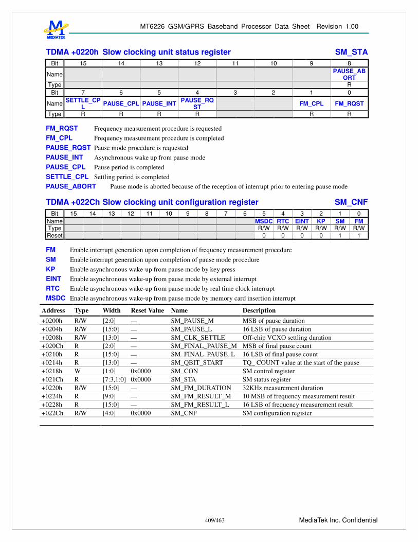
MT6226 GSM/GPRS Baseband Processor Data Sheet Revision 1.00
409/463 MediaTek Inc. Confidential
TDMA +0220h Slow clocking unit status register SM_STA Bit 15 14 13 12 11 10 9 8
Name PAUSE_ABORT
Type R Bit 7 6 5 4 3 2 1 0
Name SETTLE_CPL PAUSE_CPL PAUSE_INT PAUSE_RQ
ST FM_CPL FM_RQST
Type R R R R R R
FM_RQST Frequency measurement procedure is requested FM_CPL Frequency measurement procedure is completed PAUSE_RQST Pause mode procedure is requested PAUSE_INT Asynchronous wake up from pause mode PAUSE_CPL Pause period is completed SETTLE_CPL Settling period is completed PAUSE_ABORT Pause mode is aborted because of the reception of interrupt prior to entering pause mode
TDMA +022Ch Slow clocking unit configuration register SM_CNF Bit 15 14 13 12 11 10 9 8 7 6 5 4 3 2 1 0
Name MSDC RTC EINT KP SM FM Type R/W R/W R/W R/W R/W R/W Reset 0 0 0 0 1 1
FM Enable interrupt generation upon completion of frequency measurement procedure SM Enable interrupt generation upon completion of pause mode procedure KP Enable asynchronous wake-up from pause mode by key press EINT Enable asynchronous wake-up from pause mode by external interrupt RTC Enable asynchronous wake-up from pause mode by real time clock interrupt MSDC Enable asynchronous wake-up from pause mode by memory card insertion interrupt
Address Type Width Reset Value Name Description +0200h R/W [2:0] — SM_PAUSE_M MSB of pause duration +0204h R/W [15:0] — SM_PAUSE_L 16 LSB of pause duration +0208h R/W [13:0] — SM_CLK_SETTLE Off-chip VCXO settling duration +020Ch R [2:0] — SM_FINAL_PAUSE_M MSB of final pause count +0210h R [15:0] — SM_FINAL_PAUSE_L 16 LSB of final pause count +0214h R [13:0] — SM_QBIT_START TQ_ COUNT value at the start of the pause +0218h W [1:0] 0x0000 SM_CON SM control register +021Ch R [7:3,1:0] 0x0000 SM_STA SM status register +0220h R/W [15:0] — SM_FM_DURATION 32KHz measurement duration +0224h R [9:0] — SM_FM_RESULT_M 10 MSB of frequency measurement result +0228h R [15:0] — SM_FM_RESULT_L 16 LSB of frequency measurement result +022Ch R/W [4:0] 0x0000 SM_CNF SM configuration register

MT6226 GSM/GPRS Baseband Processor Data Sheet Revision 1.00
410/463 MediaTek Inc. Confidential
11 Power, Clocks and Reset
This chapter describes the power, clock and reset management functions provided by MT6226. Together with Power Management IC (PMIC), MT6226 offers both fine and coarse resolutions of power control through software programming. With this efficient method, the developer can turn on selective resources accordingly in order to achieve optimized power consumption. The operating modes of MT6226 as well as main power states provided by the PMIC are shown in Figure 164.
Active Mode Sleep Mode
Active ModePower DownMode
Power On SoftwareProgram
SoftwareProgramPower On
SoftwareProgram
Active State Standby State
Pause Mode
CoreProcessors
CorePeripherals
Phone Power StateCore Operating Mode
Core
Figure 164 Major Phone Power States and Operating Modes for MT6226 based terminal
11.1 B2PSI
11.1.1 General Description A 3-wire B2PSI interface is used for connecting to power management IC (PMIC). This bi-directional serial bus interface allows baseband to write to or read from PMIC. The bus protocol utilizes a 16-bit format. B2PSICK is the serial bus clock and is driven by the master. B2PSIDAT is the serial data; master or slave can drive it. B2PSICS is the bus selection signal. Once the B2PSICS goes LOW, baseband starts to transfer the 4 register bits followed by a read/write bit, then waits 3 clock cycles for the PMIC B2PSI state machine to decode the operation for the next 8 data bits. The state machine should count 16 clocks to complete the data transfer.

MT6226 GSM/GPRS Baseband Processor Data Sheet Revision 1.00
411/463 MediaTek Inc. Confidential
B 2 P S IC K
B 2 P S IC K
R 3 R 2 R 1 R 0 W X X X D 7 D 6 D 5 D 4 D 3 D 2 D 1 D 0
R 3 R 2 R 1 R 0 R X X X D 7 D 6 D 5 D 4 D 3 D 2 D 1 D 0
T > 10 0 n se c
R e c eiv e I n d ex
R e gis te r D e c o d e
W r it e R e g is te r C o n te n t
R e c eiv e I n d ex
R e gis te r D e c o d e
R e a d R e g ist e r C o n te n t
B 2P S ID A T
B 2P S ID A T
B 2 P S IC S
B 2 P S IC S
Figure 165 B2PSI bus timing
11.1.2 Register Definitions
B2PSI+0000h B2PSI data register B2PSI_DATA Bit 15 14 13 12 11 10 9 8 7 6 5 4 3 2 1 0
Name B2PSI_DATA [15:0] Type R/W Reset 0
B2PSI_DATA The B2PSI DATA format contains 4 bit register + 3 bit do not care + write / read bit + 8 bit data.
0 Read operation 1 Write operation
To prevent a writing error, B2PSI_DATA must be set to 8216h before the actual data write.
B2PSI +0008h B2PSI baud rate divider register B2PSI _DIV Bit 15 14 13 12 11 10 9 8 7 6 5 4 3 2 1 0
Name B2PSI _DIV [15:0] Type R/W Reset 0
B2PSI_DIV B2PSI clock rate divisor. B2PSICK = system clock rate / div.
B2PSI+0010h B2PSI status register B2PSI_STAT Bit 15 14 13 12 11 10 9 8 7 6 5 4 3 2 1 0
Name
WRITE_SUCCES
S
READ_REA
DT
Type RC RC Reset 0 0
READ_READY Read data ready.
0 Read data is not ready yet. 1 Read data is ready. The bit is cleared by reading B2PSI_STAT register or if B2PSI initializes a new
transmit. WRITE_SUCCESS B2PSI write successfully.
0 B2PSI write is not finished yet.

MT6226 GSM/GPRS Baseband Processor Data Sheet Revision 1.00
412/463 MediaTek Inc. Confidential
1 B2PSI write has finished. The bit is cleared by reading B2PSI_STAT register or if B2PSI initializes a new transmit.
B2PSI+0014h B2PSI CS to CK time register B2PSI_TIME Bit 15 14 13 12 11 10 9 8 7 6 5 4 3 2 1 0
Name B2PSI_TIME Type R/W Reset 0
B2PSI_TIME The time interval that first B2PSICK is started after the B2PSICS is active low.
Time interval = 1/system clock * B2PSI_time.
11.1.2.1
11.2 Clocks There are two major time bases in the MT6226. For the faster one is the 13 MHz clock originating from an off-chip temperature-compensated voltage controlled oscillator (TCVCXO) that can be either 13MHz or 26MHz. This signal is the input from the SYSCLK pad then is converted to the square-wave signal. The other time base is the 32768 Hz clock generated by an on-chip oscillator connected to an external crystal. Figure 167 shows the clock sources as well as their utilizations inside the chip.
32KHzOSC
/2Clock
Squarer
AHB Bus Clock
APB Bus Clock
32KHz Clock
AHB
MCU_DIV2
CoreI/O
SYSCLK
XIN
XOUT
CLKSQ_PLD
MPLL
MPLL
USB Clock
MCUDCM
MCUCLK
52MHz
DSPDCM
DSPCLK
91MHz ~ 13MHz
52MHz ~ 13MHz
/2
DSP_DIV2
DPLL
DPLL
91MHz
UPLL
48MHz
Figure 167 Clock distributions inside the MT6226.
11.2.1 32.768 KHz Time Base The 32768 Hz clock is always running. It’s mainly used as the time base of the Real Time Clock (RTC) module, which maintains time and date with counters. Therefore, both the 32768Hz oscillator and the RTC module is powered by separate voltage supplies that shall not be powered down when the other supplies do.
In low power mode, the 13 MHz time base is turned off, so the 32768 Hz clock shall be employed to update the critical TDMA timer and Watchdog Timer. This time base is also used to clocks the keypad scanner logic.

MT6226 GSM/GPRS Baseband Processor Data Sheet Revision 1.00
413/463 MediaTek Inc. Confidential
11.2.2 13 MHz Time Base One 1/2-dividers for PLL existing to allow using 26 or 13 MHz TCVCXO.
One phase-locked loops (PLL) to generate 624Mhz clock output, then a frequency divider futher divide 8, 12, 13 to generate 78Mhz, 52Mhz, 48Mhz for three primary clocks, DSP_CLOCK, MCU_CLOCK and USB_CLOCK, respectively. This three primary clocks then feed to DSP Clock Domain and MCU Clock Domain and USB, respectively. The PLL require no off-chip components for operations and can be turn off in order to save power. After power-on, the PLLs are off by default and the source clock signal is selected through multiplexers. The software shall take cares of the PLL lock time while changing the clock selections. The PLL and usages are listed below.
DPLL supplies the DSP system clock, DSP_CLOCK. The MCU software may set the clock multiplier according to the DSP performance required.
MPLL supplies the MCU system clock, MCU_CLOCK, which paces the operations of the MCU cores, MCU memory system, and MCU peripherals as well. The outputted 52MHz clock is connected to dynamic clock manager for dynamically adjusting clock rate by digital clock divider.
Note that PLL need some time to become stable after being powered up. The software shall take cares of the PLL lock time before switching them to the proper frequency. Usually, a software loop longer than the PLL lock time is employed to deal with the problem.
For power management, the MCU software program may stop MCU Clock by setting the Sleep Control Register. Any interrupt requests to MCU can pause the sleep mode, and thus MCU return to the running mode.
AHB also can be stop by setting the Sleep Control Register. However the behavior of AHB in sleep mode is a little different from that of MCU. After entering Sleep Mode, it can be temporarily waked up by any “hreq” (bus request), and then goes back to sleep automatically after all “hreqs” de-assert. Any transactions can take place as usual in sleep mode, and it can save power while there is no transaction on it. However the penalty is losing a little system efficiency for switching on and off bus clock, but the impact is small.
11.2.3 Dynamic Clock Switch of MCU Clock Dynamic Clock Manager is implemented to allow MCU switching clock dynamically without any jitter, and enabling signal drift, and system can operate stably during any clock rate switch.
Please note that MPLL must be enabled and the frequency shall be set as 52MHz. Before switching to 52MHz clock rate, the clock from MCU DIV2 will feed through dynamic clock manager (DCM) directly. That means if MCU DIV2 is enabled, the internal clock rate is the half of SYSCLK. Contrarily, the internal clock rate is identical to SYSCLK.
However, the settings of some hardware modules is required to be changed before or after clock rate change. Software has the responsibility to change them at proper timing. The following table is list of hardware modules needed to be changed their setting during clock rate change.
Module Name Programming Sequence
EMI
1. 26M -> 52M Changing wait state before clock change. New wait state will not take effect until current EMI access is complete. Software should insert a period of time before switching clock. 2. 52M -> 26M Changing wait state after clock change.

MT6226 GSM/GPRS Baseband Processor Data Sheet Revision 1.00
414/463 MediaTek Inc. Confidential
NAND
1. 26M -> 52M Changing wait state before clock change. New wait state will not take effect until current EMI access is complete. Software should insert a period of time before switching clock. 2. 52M -> 26M Changing wait state after clock change.
LCD Change wait state while LCD in IDLE state.
AHB
1. 26M -> 52M
Change AHB EMI interface register (0x80000500) to latch mode (0) before clock switching.
2. 52M -> 26M
Change AHB EMI interface register (0x80000500) to direct couple mode (1) after clock switching.
Table 70 Programming sequence during clock switch
11.2.4 Register Definitions
CONFG+0100h PLL Frequency Register MPLL Bit 15 14 13 12 11 10 9 8 7 6 5 4 3 2 1 0
Name CALI RST SPD Type R/W R/W R/W Reset 0 0 0100
SPD Select the Internal VCO Output Clock Rate for MPLL
0100 VCO = 312mhz (13MHz x 4*6) OTHERS RESERVED
RST Reset Control of MPLL 0 Normal Operation 1 Reset the MPLL
CALI Calibration Control for MPLL
CONFG+104h DPLL Frequency register DPLL Bit 15 14 13 12 11 10 9 8 7 6 5 4 3 2 1 0
Name CALI RST SPD Type R/W R/W R/W Reset 0 0 1
SPD Select the Output Clock Rate for DPLL
000 Reserved 001 13MHz x 2 010 13MHz x 3 011 13MHz x 4 100 13MHz x 5 101 13MHz x 6 110 13MHz x 7

MT6226 GSM/GPRS Baseband Processor Data Sheet Revision 1.00
415/463 MediaTek Inc. Confidential
RST Reset Control of DPLL 0 Normal Operation 1 Reset the DPLL
CALI Calibration Control for DPLL
CONFG+108h Clock Control Register CLK_CON Bit 15 14 13 12 11 10 9 8 7 6 5 4 3 2 1 0
Name DSP_EXTC
K
USB_EXTC
K UPLL
_TMA MPLL_TMA
DPLL_TMA
CLKSQ_PL
D
MCU_DIV2 DPLL MPLL DSP_
DIV2
Type R/W R/W R/W R/W R/W R/W R/W R/W R/W R/W Reset 0 0 0 0 0 0 0 0 0 0
DSP_EXTCK Use external DSP clock source.
0 Not use external clock. 1 Use external clock. USB_EXTCK Use external USB clock source.
0 Not use external clock. 1 Use external clock.
DSP_DIV2 Control the x2 clock divider for DPLL input 0 Divider bypassed 1 Divider not bypassed
MPLL Select MCU Clock 0 MPLL bypassed 1 Using MPLL Clock
DPLL Select DSP Clock 0 DPLL bypassed 1 Using DPLL Clock
MCU_DIV2 Control the x2 clock divider for MCU clock domain 0 Divider bypassed 1 Divider not bypassed
CLKSQ_PLD Pull Down Control 0 Disable 1 Enables
DPLL_TMA DPLL test mode 0 Disable 1 Enables
MPLL_TMA MPLL test mode 0 Disable 1 Enable
UPLL_TMA UPLL test mode 0 Disable 1 Enable
CONFG+10Ch Sleep Control Register SLEEP_CON Bit 15 14 13 12 11 10 9 8 7 6 5 4 3 2 1 0

MT6226 GSM/GPRS Baseband Processor Data Sheet Revision 1.00
416/463 MediaTek Inc. Confidential
Name DSP AHB MCU Type WO WO WO Reset 0 0 0
MCU Stop the MCU Clock to force MCU Processor entering sleep mode. MCU clock will be resumed as long as there
comes an interrupt request or system is reset. 0 MCU Clock is running 1 MCU Clock is stopped
AHB Stop the AHB Bus Clock to force the entire bus entering sleep mode. AHB clock will be resumed as long as there comes an interrupt request or system is reset. 0 AHB Bus Clock is running 1 AHB Bus Clock is stopped
DSP Stop the DSP Clock. 0 DSP Bus Clock is running 1 DSP Bus Clock is stopped
CONFG+0114h MCU Clock Control Register MCUCLK_CON Bit 15 14 13 12 11 10 9 8 7 6 5 4 3 2 1 0
Name FSEL Type R/W Reset 3
FSEL MCU clock frequency selection. This control register is used to control the output clock frequency of Dynamic
Clock Manager. The clock frequency is from 13MHz to 52MHz. The waveform of the output clock is shown below.
Please note that the clock period of 39MHz is not uniform. The shortest period of 39MHz clock is the same as the period of 52MHz. As a result, the wait states of external interfaces, such as EMI, NAND, and so on, have to be configured based on 52MHz timing. Therefore, the MCU performance executing in external memory at 39MHz may be worse than at 26MHz. Also note that the maximum latency of clock switch is 4 clock periods. Software shall provide 4T locking time after clock switch command.
52M39M26M13M
Figure 168 Output of Dynamic Clock Manager
0 13MHz 1 26MHz 2 39MHz 3 52MHz Others reserved

MT6226 GSM/GPRS Baseband Processor Data Sheet Revision 1.00
417/463 MediaTek Inc. Confidential
11.3 Reset Generation Unit (RGU) Figure 169 shows the reset scheme used in MT6226. MT6226 provides three kinds of resets: hardware reset, watchdog reset, and software reset.
Figure 169 Reset Scheme Used in MT6226
11.3.1 General Description
11.3.1.1 Hardware Reset
This reset is input through the SYSRST# pin, which is driven low during power-on. The hardware reset has a global effect on the chip: all digital and analog circuits are initialized, except the Real Time Clock module. The initial states of the MT6226 sub-blocks are as follows:.
All analog circuits are turned off.
All PLLs are turned off and bypassed. The 13 MHz system clock is the default time base.
Special trap states in GPIO.
11.3.1.2 Watchdog Reset
A watchdog reset is generated when the Watchdog Timer expires: the MCU software failed to re-program the timer counter in time. This situation is typically induced by abnormal software execution, which can be aborted by a hardwired watchdog reset. Hardware blocks that are affected by the watchdog reset are:
MCU subsystem,
DSP subsystem, and
External components (trigged by software).

MT6226 GSM/GPRS Baseband Processor Data Sheet Revision 1.00
418/463 MediaTek Inc. Confidential
11.3.1.3 Software Resets
Software resets are local reset signals that initialize specific hardware components. For example, if hardware failures are detected, the MCU or DSP software may write to software reset trigger registers to reset those specific hardware modules to their initial states.
The following modules have software resets.
DSP Core
DSP Coprocessors
11.3.2 Register Definitions
RGU +0000h Watchdog Timer Control Register WDT_MODE Bit 15 14 13 12 11 10 9 8 7 6 5 4 3 2 1 0
Name KEY[7:0] AUTO-RESTART
IRQ EXTEN
EXTPOL
ENABLE
Type R/W R/W R/W R/W R/W Reset 0 0 0 0 1
ENABLE Enables the Watchdog Timer.
0 Disables the Watchdog Timer. 1 Enables the Watchdog Timer.
EXTPOL Defines the polarity of the external watchdog pin. 0 Active low.
1 Active high. EXTEN Specifies whether or not to generate an external watchdog reset signal.
0 The watchdog does not generate an external watchdog reset signal. 1 If the watchdog counter reaches zero, an external watchdog signal is generated.
IRQ Issues an interrupt instead of a Watchdog Timer reset. For debug purposes, RGU issues an interrupt to the MCU instead of resetting the system. 0 Disable. 1 Enable.
AUTO-RESTART Restarts the Watchdog Timer counter with the value of WDT_LENGTH while task ID is written into Software Debug Unit. 0 Disable. The counter restarts by writing KEY into the WDT_RESTART register.
1 Enable. The counter restarts by writing KEY into the WDT_RESTART register or by writing task ID into the software debug unit.
KEY Write access is allowed if KEY=0x22.
RGU +0004h Watchdog Time-Out Interval Register WDT_LENGTH Bit 15 14 13 12 11 10 9 8 7 6 5 4 3 2 1 0
Name TIMEOUT[10:0] KEY[4:0] Type WO Reset 111_1111_1111b
KEY Write access is allowed if KEY=08h.

MT6226 GSM/GPRS Baseband Processor Data Sheet Revision 1.00
419/463 MediaTek Inc. Confidential
TIMEOUT The counter is restarted with TIMEOUT [10:0], 1_1111_1111b. Thus the Watchdog Timer time-out period is a multiple of 512*T32k=15.6ms.
RGU +0008h Watchdog Timer Restart Register WDT_RESTART Bit 15 14 13 12 11 10 9 8 7 6 5 4 3 2 1 0
Name KEY[15:0] Type Reset
KEY Restart the counter if KEY=1971h.
RGU +000Ch Watchdog Timer Status Register WDT_STA Bit 15 14 13 12 11 10 9 8 7 6 5 4 3 2 1 0
Name WDT SW_WDT
Type RO RO Reset 0 0
WDT Indicates the cause of the watchdog reset.
0 Reset not due to Watchdog Timer. 1 Reset because the Watchdog Timer time-out period expired.
SW_WDT Indicates if the watchdog was triggered by software. 0 Reset not due to software-triggered Watchdog Timer. 1 Reset due to software-triggered Watchdog Timer.
NOTE: A system reset does not affect this register. This bit is cleared when the WTU_MODE register ENABLE bit is written.
RGU +0010h CPU Peripheral Software Reset Register SW_PERIPH_RS
TN Bit 15 14 13 12 11 10 9 8 7 6 5 4 3 2 1 0
Name DAMRST
USBRST
KEY
Type R/W R/W Reset 0 0
KEY Write access is allowed if KEY=37h. DMARST Reset the DMA peripheral.
0 No reset. 1 Invoke a reset.
USBRST Reset the USB. 0 No reset.
1 Invoke a reset.
RGU +0014h DSP Software Reset Register SW_DSP_RSTN Bit 15 14 13 12 11 10 9 8 7 6 5 4 3 2 1 0
Name RST Type R/W Reset 0
RST Controls the DSP System Reset Control.

MT6226 GSM/GPRS Baseband Processor Data Sheet Revision 1.00
420/463 MediaTek Inc. Confidential
0 No reset. 1 Invoke a reset.
RGU +0018h Watchdog Timer Reset Signal Duration Register WDT_RSTINTRE
VAL Bit 15 14 13 12 11 10 9 8 7 6 5 4 3 2 1 0
Name LENGTH[ 11:0] Type R/W Reset FFFh
LENGTH This register indicates the reset duration when Watchdog Timer times out. However, if the WDT_MODE
register IRQ bit is set to 1, an interrupt is issued instead of a reset.
RGU+001Ch Watchdog Timer Software Reset Register WDT_SWRST Bit 15 14 13 12 11 10 9 8 7 6 5 4 3 2 1 0
Name KEY[15:0] Type Reset
Software-triggered Watchdog Timer reset. If the register content matches the KEY, a watchdog reset is issued. However, if the WDT_MODE register IRQ bit is set to 1, an interrupt is issued instead of a reset.
KEY 1209h
11.4 Software Power Down Control In addition to Pause Mode capability during Standby State, the software program can also put each peripheral independently into Power Down Mode during Active State by gating off their clock. The typical logic implementation is depicted as in Figure 171. For all of the configuration bits, 1 means that the function is in Power Down Mode and 0 means that it is in the Active Mode.
CLOCK
POWER DOWNTESTMODE
Figure 171 Power Down Control at Block Level
11.4.1 Register Definitions
CONFG+300h Power Down Control 0 Register PDN_CON0 Bit 15 14 13 12 11 10 9 8 7 6 5 4 3 2 1 0
Name DSP_DIV2 MPLL DPLL MCU_
DIV2 CLKS
Q SE WAVETABL
E GCU USB DMA
Type R/W R/W R/W R/W R/W R/W R/W R/W R/W R/W

MT6226 GSM/GPRS Baseband Processor Data Sheet Revision 1.00
421/463 MediaTek Inc. Confidential
Reset 1 1 1 1 0 1 1 1 1 1
DMA Controls the DMA Controller Power Down USB Controls the USB Controller Power Down GCU Controls the GCU Controller Power Down WAVETABLE Controls the DSP Wave-Table DMA Power Down SE Controls the security engine Power Down CLKSQ Controls the Clock squarer Power Down MCU_DIV2 Controls the MUC DIV2 Power Down DPLL Controls the DPLL Power Down MPLL Controls the MPLL Power Down DSP_DIV2 Controls the DSP DIV2 Power Down
CONFG +304h Power Down Control 1 Register PDN_CON1 Bit 15 14 13 12 11 10 9 8 7 6 5 4 3 2 1 0
Name IRDA UART3 B2PSI NFI PWM2 MSDC UART
2 LCD ALTER PWM SIM UART
1 GPIO KP GPT
Type R/W R/W R/W R/W R/W R/W R/W R/W R/W R/W R/W R/W R/W R/W R/W Reset 1 1 1 1 1 1 1 1 1 1 1 0 1 1 1
GPT Controls the General Purpose Timer Power Down KP Controls the Keypad Scanner Power Down GPIO Controls the GPIO Power Down UART1 Controls the UART1 Controller Power Down SIM Controls the SIM Controller Power Down PWM Controls the PWM Generator Power Down ALTER Controls the Alerter Generator Power Down LCD Controls the Serial LCD Controller Power Down UART2 Controls the UART2 Controller Power Down MSDC Controls the MS/SD Controller Power Down PWM2 Controls the PWM2 Generator Power Down NFI Controls the NAND FLASH Interface Power Down B2PSI Controls the Serial Port Interface Power Down UART3 Controls the UART3 Controller Power Down IRDA Controls the IrDA Framer Power Down
CONFG +308h Power Down Control 2 Register PDN_CON2 Bit 15 14 13 12 11 10 9 8 7 6 5 4 3 2 1 0
Name GMSK BBRX SCCB AAFE DIV GCC BFE VAFE AUXAD FCS APC AFC BPI BSI RTC TDMA
Type R/W R/W R/W R/W R/W R/W R/W R/W R/W R/W R/W R/W R/W R/W R/W R/W Reset 1 1 1 1 1 1 1 1 1 1 1 1 1 1 1 1
TDMA Controls the TDMA Power Down RTC Controls the RTC Power Down BSI Controls the BSI Power Down. This control will not be updated until both tdma_evtval and qbit_en are asserted. BPI Controls the BPI Power Down. This control will not be updated until both tdma_evtval and qbit_en are asserted. AFC Controls the AFC Power Down. This control will not be updated until both tdma_evtval and qbit_en are asserted.

MT6226 GSM/GPRS Baseband Processor Data Sheet Revision 1.00
422/463 MediaTek Inc. Confidential
APC Controls the APC Power Down. This control will not be updated until both tdma_evtval and qbit_en are asserted. FCS Controls the FCS Power Down AUXAD Controls the AUX ADC Power Down VAFE Controls the Audio Front End of VBI Power Down BFE Controls the Base-Band Front End Power Down GCU Controls the GCU Power Down DIV Controls the Divider Power Down AAFE Controls the Audio Front End of MP3 Power Down SCCB Controls the SCCB Power Down BBRX Controls the BB RX Power Down GMSK Controls the GMSK Power Down
CONFG +30Ch Power Down Control 3 Register PDN_CON3 Bit 15 14 13 12 11 10 9 8 7 6 5 4 3 2 1 0
Name IMGDMA DCT ISP RESZ JPEG MP4 G2D GCMQ IMGP
ROC ICE
Type R/W R/W R/W R/W R/W R/W R/W R/W R/W R/W Reset 1 1 1 1 1 1 1 1 1 1
ICE Enables the debug feature of the ARM7EJS core. It controls the DBGEN pin of the ICEBreaker. IMGPROC Controls the Image Processor Power Down GCMQ Controls the Graphic Command Queue Power Down G2D Controls the 2D Accelerator Power Down MP4 Controls the MPEG-4 Power Down JPEG Controls the JPEG Power Down RESZ Controls the Resizer Power Down ISP Controls the Image Signal Processor Power Down DCT Controls the DCT Power Down IMGDMA Controls the Image DMA Power Down
CONFG+0310h Power Down Set 0 Register PDN_SET0 Bit 15 14 13 12 11 10 9 8 7 6 5 4 3 2 1 0
Name DSP_DIV2 MPLL DPLL MCU_
DIV2 CLKS
Q SE WAVETABL
E GCU USB DMA
Type W1S W1S W1S W1S W1S W1S W1S W1S W1S W1S W1S W1S W1S W1S W1S W1S
CONFG+0314h Power Down Set 1 Register PDN_SET1 Bit 15 14 13 12 11 10 9 8 7 6 5 4 3 2 1 0
Name IRDA UART3 B2PSI NFI PWM2 MSDC UART
2 LCD ALTER PWM SIM UART
1 GPIO KP GPT
Type W1S W1S W1S W1S W1S W1S W1S W1S W1S W1S W1S W1S W1S W1S W1S W1S
CONFG+0318h Power Down Set 2 Register PDN_SET2 Bit 15 14 13 12 11 10 9 8 7 6 5 4 3 2 1 0
Name GMSK BBRX SCCB AAFE DIV GCC BFE VAFE AUXAD FCS APC AFC BPI BSI RTC TDMA
Type W1S W1S W1S W1S W1S W1S W1S W1S W1S W1S W1S W1S W1S W1S W1S W1S

MT6226 GSM/GPRS Baseband Processor Data Sheet Revision 1.00
423/463 MediaTek Inc. Confidential
CONFG+031Ch
Power Down Set 3 Register PDN_SET3
Bit 15 14 13 12 11 10 9 8 7 6 5 4 3 2 1 0
Name IMGDMA DCT CAM RESZ JPEG MP4 G2D GCMQ IMGP
ROC ICE
Type W1S W1S W1S W1S W1S W1S W1S W1S W1S W1S W1S W1S W1S W1S
These registers are used to individually set power down control bit. Only the bits set to 1 are in effect. Setting the bits to 1 also sets the corresponding power down control bits will to 1. Otherwise, the bits keep their original value.
EACH BIT Set the Associated Power Down Control Bit to 1. 0 no effect 1 Set corresponding bit to 1
CONFG+0320h Power Down Clear 0 Register PDN_CLR0 Bit 15 14 13 12 11 10 9 8 7 6 5 4 3 2 1 0
Name DSP_DIV2 MPLL DPLL MCU_
DIV2 CLKS
Q SE WAVETABL
E GCU USB DMA
Type W1C W1C W1C W1C W1C W1C W1C W1C W1C W1C W1C W1C W1C W1C W1C W1C
CONFG+0324h Power Down Clear 1 Register PDN_CLR1 Bit 15 14 13 12 11 10 9 8 7 6 5 4 3 2 1 0
Name IRDA UART3 B2PSI NFI PWM2 MSDC UART
2 LCD ALTER PWM1 SIM UART
1 GPIO KP GPT
Type W1C W1C W1C W1C W1C W1C W1C W1C W1C W1C W1C W1C W1C W1C W1C W1C
CONFG+0328h Power Down Clear 2 Register PDN_CLR2 Bit 15 14 13 12 11 10 9 8 7 6 5 4 3 2 1 0
Name GMSK BBRX SCCB AAFE DIV GCC BFE VAFE AUXAD FCS APC AFC BPI BSI RTC TDMA
Type W1C W1C W1C W1C W1C W1C W1C W1C W1C W1C W1C W1C W1C W1C W1C W1C
CONFG+032Ch
Power Down Clear 3 Register PDN_CLR3
Bit 15 14 13 12 11 10 9 8 7 6 5 4 3 2 1 0
Name IMGDMA DCT CAM RESZ JPEG MP4 G2D GCMQ IMGP
ROC ICE
Type W1C W1C W1C W1C W1C W1C W1C W1C W1C W1C W1C W1C W1C W1C
These registers are used to individually clear power down control bit. Only the bits set to 1 are in effect. Setting the bits to 1 also sets the corresponding power down control bits to 0. Otherwise, the bits keep their original value.
EACH BIT Clear the Associated Power Down Control Bit. 0 no effect 1 Set corresponding bit to 0

MT6226 GSM/GPRS Baseband Processor Data Sheet Revision 1.00
424/463 MediaTek Inc. Confidential
12 Analog Front-end & Analog Blocks
12.1 General Description To communicate with analog blocks, a common control interface for all analog blocks is implemented. In addition, there are some dedicated interfaces for data transfer. The common control interface translates APB bus write and read cycle for specific addresses related to analog front-end control. Dedicated data interface of each analog block is implemented in the corresponding digital block. The Analog Blocks includes the following analog function for complete GSM/GPRS base-band signal processing:
1. Base-band RX: For I/Q channels base-band A/D conversion
2. Base-band TX: For I/Q channels base-band D/A conversion and smoothing filtering, DC level shifting
3. RF Control: Two DACs for automatic power control (APC) and automatic frequency control (AFC) are included. Their outputs are provided to control external RF power amplifier and VCXO output frequency, respectively.
4. Auxiliary ADC: Providing an ADC for battery and other auxiliary analog function monitoring
5. Audio mixed-signal blocks: It provides complete analog voice signal processing including microphone amplification, A/D conversion, D/A conversion, earphone driver, and etc. Besides, dedicated stereo D/A conversion and amplification for audio signals are included.
6. Clock Generation: A clock squarer for shaping system clock, and two PLLs that provide clock signals to MCU/USB, and DSP units are included
7. XOSC32: It is a 32-KHz crystal oscillator circuit for RTC and low power application.
12.1.1 BBRX
12.1.1.1 Block Descriptions
The receiver (RX) performs base-band I/Q channels downlink analog-to-digital conversion:
1. Analog input multiplexer: For each channel, a 4-input multiplexer that supports offset and gain calibration is included.
2. A/D converter: Two 14-bit sigma-delta ADCs perform I/Q digitization for further digital signal processing.
12.1.1.2 Functional Specifications
The functional specifications of the base-band downlink receiver are listed in the following table.
Symbol Parameter Min Typical Max Unit
N Resolution 14 Bit
FC Clock Rate 26 MHz
FS Output Sampling Rate 13/12 MSPS
Input Swing When GAIN=’0’ When GAIN=’1’
0.8*AVDD 0.4*AVDD
Vpk Vpk

MT6226 GSM/GPRS Baseband Processor Data Sheet Revision 1.00
425/463 MediaTek Inc. Confidential
OE Offset Error +/- 10 mV
FSE Full Swing Error +/- 30 mV
I/Q Gain Mismatch 0.5 dB
SINAD Signal to Noise and Distortion Ratio - 45kHz sine wave in [0:90] kHz bandwidth - 145kHz sine wave in [10:190] kHz
bandwidth
65 65
dB dB
ICN Idle channel noise - [0:90] kHz bandwidth - [10:190] kHz bandwidth
-74 -70
dB dB
DR Dynamic Range - [0:90] kHz bandwidth - [10:190] kHz bandwidth
74 70
dB dB
RIN Input Resistance 75 k
DVDD Digital Power Supply 1.6 1.8 2.0 V
AVDD Analog Power Supply 2.5 2.8 3.1 V
T Operating Temperature 0 60 125
Current Consumption Power-up Power-Down
5 5
mA A
Table 71 Base-band Downlink Specifications
12.1.2 BBTX
12.1.2.1 Block Descriptions
The transmitter (TX) performs base-band I/Q channels up-link digital-to-analog conversion. Each channel includes:
1. 10-Bits D/A Converter: It converts digital GMSK modulated signals to analog domain. The input to the DAC is sampled at 4.33-MHz rate with 10-bits resolution.
2. Smoothing Filter: The low-pass filter performs smoothing function for DAC output signals with a 350-kHz 2nd-order Butterworth frequency response.
12.1.2.2 Function Specifications
The functional specifications of the base-band uplink transmitter are listed in the following table.
Symbol Parameter Min Typical Max Unit
N Resolution 10 Bit
FS Sampling Rate 4.33 MSPS
SINAD Signal to Noise and Distortion Ratio 57 60 dB
Output Swing 0.18*AVDD 0.89*AVDD V
VOCM Output CM Voltage 0.34*AVDD 0.5*AVDD 0.62*AVDD V
Output Capacitance 20 PF

MT6226 GSM/GPRS Baseband Processor Data Sheet Revision 1.00
426/463 MediaTek Inc. Confidential
Output Resistance 10 K
DNL Differential Nonlinearity +/- 0.5 LSB
INL Integral Nonlinearity +/- 1.0 LSB
OE Offset Error +/- 15 mV
FSE Full Swing Error +/- 30 mV
FCUT Filter –3dB Cutoff Frequency 300 350 400 KHz
ATT Filter Attenuation at 100-KHz 270-KHz 4.33-MHz
0.1 2.2 46.4
0.0 1.3 43.7
0.0 0.8 41.4
dB dB dB
I/Q Gain Mismatch +/- 0.5 dB
I/Q Gain Mismatch Correction Range -1.18 +1.18 dB
DVDD Digital Power Supply 1.6 1.8 2.0 V
AVDD Analog Power Supply 2.5 2.8 3.1 V
T Operating Temperature 0 60 125
Current Consumption Power-up Power-Down
5 5
mA A
Table 72 Base-band Uplink Transmitter Specifications
12.1.3 AFC-DAC
12.1.3.1 Block Descriptions
As shown in the following figure, together with a 2nd-oder digital sigma-delta modulator, AFC-DAC is designed to produce a single-ended output signal at AFC pin. AFC pin should be connected to an external 1st-order R-C low pass filter to meet the 13-bits resolution (DNL) requirement2.
The AFC_BYP pin is the mid-tap of a resistor divider inside the chip to offer the AFC output common-mode level. Nominal value of this common-mode voltage is half the analog power supply, and typical value of output impedance of AFC_BYP pin is about 21k. To suppress the noise on common mode level, it is suggested to add an external capacitance between AFC_BYP pin and ground. The value of the bypass capacitor should be chosen as large as possible but still meet the settling time requirement set by overall AFC algorithm3.
2 DNL performance depends on external output RC filter bandwidth: the narrower the bandwidth, the better the DNL. Thus, there exists a tradeoff between output setting speed and DNL performance
3 AFC_BYP output impedance and bypass capacitance determine the common-mode settling RC time constant. Insufficient common-mode settling will affect the INL performance. A typical value of 1nF is suggested.

MT6226 GSM/GPRS Baseband Processor Data Sheet Revision 1.00
427/463 MediaTek Inc. Confidential
12.1.3.2 Functional Specifications
The following table gives the electrical specification of AFC-DAC.
Symbol Parameter Min Typical Max Unit
N Resolution 13 Bit
FS Sampling Rate 6500 KHz
DVDD Digital Power Supply 1.6 1.8 2.0 V
AVDD Analog Power Supply 2.6 2.8 3.1 V
T Operating Temperature 0 60 125
Current Consumption Power-up Power-Down
1.2
1 mA A
Output Swing 0.75*AVDD V
Output Resistor (in AFC output RC network)
1 K
DNL Differential Nonlinearity +1/-1 LSB
INL Integral Nonlinearity +4.0/-4.0 LSB
Table 73 Functional specification of AFC-DAC
12.1.4 APC-DAC
12.1.4.1 Block Descriptions
The APC-DAC is a 10-bits DAC with output buffer aimed for automatic power control. Here blow are its analog pin assignment and functional specification tables.
12.1.4.2 Function Specifications
Symbol Parameter Min Typical Max Unit
N Resolution 10 Bit
FS Sampling Rate 1.0833 MSPS
SINAD Signal to Noise and Distortion Ratio (10-KHz Sine with 1.0V Swing & 100-KHz BW)
50 dB
99% Settling Time (Full Swing on Maximal Capacitance) 5 S
Output Swing AVDD-0.2 V
Output Capacitance 200 pF
Output Resistance 10 K
DNL Differential Nonlinearity +/- 0.5 LSB
INL Integral Nonlinearity +/- 1.0 LSB
OE Offset Error +/- 10 mV
FSE Full Swing Error +/- 10 mV
DVDD Digital Power Supply 1.6 1.8 2.0 V

MT6226 GSM/GPRS Baseband Processor Data Sheet Revision 1.00
428/463 MediaTek Inc. Confidential
AVDD Analog Power Supply 2.5 2.8 3.1 V
T Operating Temperature 0 60 125
Current Consumption Power-up Power-Down
600 1
A A
Table 74 APC-DAC Specifications
12.1.5 Auxiliary ADC
12.1.5.1 Block Descriptions
The auxiliary ADC includes the following functional blocks:
1. Analog Multiplexer: The analog multiplexer selects signal from one of the seven auxiliary input pins. Real world messages to be monitored, like temperature, should be transferred to the voltage domain.
2. 10 bits A/D Converter: The ADC converts the multiplexed input signal to 10-bit digital data.
12.1.5.2 Function Specifications
The functional specifications of the auxiliary ADC are listed in the following table.
Symbol Parameter Min Typical Max Unit
N Resolution 10 Bit
FC Clock Rate 0.1 1.0833 5 MHz
FS Sampling Rate @ N-Bit 5/(N+1) MSPS
Input Swing 1.0 AVDD V
VREFP Positive Reference Voltage (Defined by AUX_REF pin)
1.0 AVDD V
CIN Input Capacitance Unselected Channel Selected Channel
50 1.2
fF pF
RIN Input Resistance Unselected Channel Selected Channel
10 1.8
M M
RS Resistor String Between AUX_REF pin & ground Power Up Power Down
35 10
50 65 K M
Clock Latency 11 1/FC
DNL Differential Nonlinearity +0.5/-0.5 LSB
INL Integral Nonlinearity +1.0/-1.0 LSB
OE Offset Error +/- 10 mV
FSE Full Swing Error +/- 10 mV
SINAD Signal to Noise and Distortion Ratio (10-KHz Full Swing Input & 13-MHz Clock Rate)
50 dB

MT6226 GSM/GPRS Baseband Processor Data Sheet Revision 1.00
429/463 MediaTek Inc. Confidential
DVDD Digital Power Supply 1.6 1.8 2.0 V
AVDD Analog Power Supply 2.5 2.8 3.1 V
T Operating Temperature 0 60 125
Current Consumption Power-up Power-Down
300 1
A A
Table 75 The Functional specification of Auxiliary ADC
12.1.6 Audio mixed-signal blocks
12.1.6.1 Block Descriptions
Audio mixed-signal blocks (AMB) integrate complete voice uplink/downlink and audio playback functions. As shown in the following figure, it includes mainly three parts. The first consists of stereo audio DACs and speaker amplifiers for audio playback. The second is the voice downlink path, including voice-band DACs and amplifiers, which produces voice signal to earphone or other auxiliary output device. Amplifiers in these two blocks are equipped with multiplexers to accept signals from internal audio/voice or external radio sources. The last is the voice uplink path, which is the interface between microphone (or other auxiliary input device) input and MT6226 DSP. A set of bias voltage is provided for external electret microphone..

MT6226 GSM/GPRS Baseband Processor Data Sheet Revision 1.00
430/463 MediaTek Inc. Confidential
MU
XM
UX
Stereo-to-Mono
Stereo-to-Mono
VoiceSignal
AudioSignal
Voice Amp-0
Audio Amp-R
Audio Amp-L
MU
X
VoiceSignal
AudioLCH-DAC
AudioRCH-DAC
Voice DAC
Voice ADC
PGA
Figure 172 Block diagram of audio mixed-signal blocks.
12.1.6.2 Functional Specifications
The following table gives functional specifications of voice-band uplink/downlink blocks.
Symbol Parameter Min Typical Max Unit
FS Sampling Rate 4096 KHz
CREF Decoupling Cap Between AU_VREF_P And AU_VREF_N
47 NF
DVDD Digital Power Supply 1.6 1.8 2.0 V
AVDD Analog Power Supply 2.5 2.8 3.1 V
T Operating Temperature 0 60 125
IDC Current Consumption 5 mA
VMIC Microphone Biasing Voltage 1.9 V
IMIC Current Draw From Microphone Bias 2 mA

MT6226 GSM/GPRS Baseband Processor Data Sheet Revision 1.00
431/463 MediaTek Inc. Confidential
Pins
Uplink Path4
SINAD Signal to Noise and Distortion Ratio Input Level: -40 dbm0 Input Level: 0 dbm0
29
69
dB dB
RIN Input Impedance (Differential) 13 20 27 K
ICN Idle Channel Noise -67 dBm0
XT Crosstalk Level -66 dBm0
Downlink Path5
SINAD Signal to Noise and Distortion Ratio Input Level: -40 dBm0 Input Level: 0 dBm0
29
69 dB dB
RLOAD Output Resistor Load (Differential) 28
CLOAD Output Capacitor Load 200 pF
ICN Idle Channel Noise of Transmit Path -67 dBm0
XT Crosstalk Level on Transmit Path -66 dBm0
Table 76 Functional specifications of analog voice blocks
Functional specifications of the audio blocks are described in the following.
Symbol Parameter Min Typical Max Unit FCK Clock Frequency Fs*128 KHz
Fs Sampling Rate 32 44.1 48 KHz
AVDD Power Supply 2.6 2.8 3.1 V
T Operating Temperature 0 60 125
IDC Current Consumption 5 mA
PSNR Peak Signal to Noise Ratio 80 dB
DR Dynamic Range 80 dB
VOUT Output Swing for 0dBFS Input Level 0.85 Vrms
THD Total Harmonic Distortion
45mW at 16 Load
-40
-60
dB dB
4 For uplink-path, not all gain setting of VUPG meets the specification listed on table, especially for the several highest gains. The maximum gain that meets the specification is to be determined.
5 For downlink-path, not all gain setting of VDPG meets the specification listed on table, especially for the several lowest gains. The minimum gain that meets the specification is to be determined.

MT6226 GSM/GPRS Baseband Processor Data Sheet Revision 1.00
432/463 MediaTek Inc. Confidential
22mW at 32 Load
RLOAD Output Resistor Load (Single-Ended) 16
CLOAD Output Capacitor Load 200 pF
XT L-R Channel Cross Talk TBD dB
Table 77 Functional specifications of the analog audio blocks
12.1.7 Clock Squarer
12.1.7.1 Block Descriptions
For most VCXO, the output clock waveform is sinusoidal with too small amplitude (about several hundred mV) to make MT6226 digital circuits function well. Clock squarer is designed to convert such a small signal to a rail-to-rail clock signal with excellent duty-cycle. It provides also a pull-down function when the circuit is powered-down.
12.1.7.2 Function Specifications
The functional specification of clock squarer is shown in Table 78.
Symbol Parameter Min Typical Max Unit
Fin Input Clock Frequency 13 MHz
Fout Output Clock Frequency 13 MHz
Vin Input Signal Amplitude 500 AVDD mVpp
DcycIN Input Signal Duty Cycle 50 %
DcycOUT Output Signal Duty Cycle DcycIN-5 DcycIN+5 %
TR Rise Time on Pin CLKSQOUT 5 ns/pF
TF Fall Time on Pin CLKSQOUT 5 ns/pF
DVDD Digital Power Supply 1.3 1.5 1.7 V
AVDD Analog Power Supply 2.5 2.8 3.1 V
T Operating Temperature 0 60 125
Current Consumption TBD A
Table 78 The Functional Specification of Clock Squarer
12.1.7.3 Application Notes
Here below in the figure is an equivalent circuit of the clock squarer. Please be noted that the clock squarer is designed to accept a sinusoidal input signal. If the input signal is not sinusoidal, its harmonic distortion should be low enough to not produce a wrong clock output. As an reference, for a 13MHz sinusoidal signal input with amplitude of 0.2V the harmonic distortion should be smaller than 0.02V.

MT6226 GSM/GPRS Baseband Processor Data Sheet Revision 1.00
433/463 MediaTek Inc. Confidential
Figure 173 Equivalent circuit of Clock Squarer.
12.1.8 Phase Locked Loop
12.1.8.1 Block Descriptions
MT6226 includes two PLLs: DSP PLL and MCU/USB PLL. DSP PLL can provide up to 91MHz or any other output clock frequency that is multiples of 13MHz. The MCU/USB PLL can provide 52MHz for MCU and 48MHz for USB-related application while the input frequency is 13MHz.
12.1.8.2 Function Specifications
The functional specification of DSP PLL is shown in the following table.
Symbol Parameter Min Typical Max Unit
Fin Input Clock Frequency 13 MHz
Fout Output Clock Frequency 26 91 MHz
Lock-in Time TBD s
Output Clock Duty Cycle 40 50 60 %
Output Clock Jitter 650 ps
DVDD Digital Power Supply 1.6 1.8 2.0 V
AVDD Analog Power Supply 2.5 2.8 3.1 V
T Operating Temperature 0 60 125
Current Consumption TBD A
Table 79 The Functional Specification of DSP PLL
The functional specification of MCU PLL is shown below.
Symbol Parameter Min Typical Max Unit
Fin Input Clock Frequency 4 MHz
Fout Output Clock Frequency 52 MHz
Lock-in Time TBD s
Output Clock Duty Cycle 40 50 60 %
Output Clock Jitter 650 ps

MT6226 GSM/GPRS Baseband Processor Data Sheet Revision 1.00
434/463 MediaTek Inc. Confidential
DVDD Digital Power Supply 1.3 1.5 1.7 V
AVDD Analog Power Supply 2.5 2.8 3.1 V
T Operating Temperature 0 60 125
Current Consumption TBD A
Table 80 The Functional Specification of MCU/USB PLL (MCU clock)
The functional specification of USB PLL is shown below.
Symbol Parameter Min Typical Max Unit
Fin Input Clock Frequency 4 MHz
Fout Output Clock Frequency 48 MHz
Lock-in Time TBD s
Output Clock Duty Cycle 40 50 60 %
Output Clock Jitter 650 ps
DVDD Digital Power Supply 1.3 1.5 1.7 V
AVDD Analog Power Supply 2.5 2.8 3.1 V
T Operating Temperature 0 60 125
Current Consumption TBD A
Table 81 The Functional Specification of MCU/USB PLL (USB clock)
12.1.9 32-KHz Crystal Oscillator
12.1.9.1 Block Descriptions
The low-power 32-KHz crystal oscillator XOSC32 is designed to work with an external piezoelectric 32.768kHz crystal and a load composed of two functional capacitors, as shown in the following figure.
Figure 174 Block diagram of XOSC32
12.1.9.2 Functional specifications
The functional specification of XOSC32 is shown in the following table.
Symbol Parameter Min Typical Max Unit

MT6226 GSM/GPRS Baseband Processor Data Sheet Revision 1.00
435/463 MediaTek Inc. Confidential
AVDDRTC Analog power supply 1.2 1.5 2 V
Tosc Start-up time 5 sec
Dcyc Duty cycle 50 %
TR Rise time on XOSCOUT TBD ns/pF
TF Fall time on XOSCOUT TBD ns/pF
Current consumption 5 A
Leakage current 1 A
T Operating temperature 0 60 125
Table 82 Functional Specification of XOSC32
Here below are a few recommendations for the crystal parameters for use with XOSC32.
Symbol Parameter Min Typical Max Unit
F Frequency range 32768 Hz
GL Drive level 5 uW
f/f Frequency tolerance +/- 20 Ppm
ESR Series resistance 50 K
C0 Static capacitance 1.6 pF
CL6 Load capacitance 6 12.5 pF Table 83 Recommended Parameters of the 32kHz crystal
12.2 MCU Register Definitions
12.2.1 BBRX MCU APB bus registers for BBRX ADC are listed as followings.
MIXED+0300h BBRX ADC Analog-Circuit Control Register BBRX_AC_CON Bit 15 14 13 12 11 10 9 8 7 6 5 4 3 2 1 0
Name QSEL ISEL RSV GAIN CALBIAS Type R/W R/W R/W R/W R/W Reset 00 00 0 00 00000
Set this register for analog circuit configuration controls.
CALBIAS The register field is for control of biasing current in BBRX mixed-signal module. It is coded in 2’s complement. That is, its maximum is 15 and minimum is –16. Biasing current in BBRX mixed-signal module has impact on the performance of A/D conversion. The larger the value of the register field, the larger the biasing current in BBRX mixed-signal module, and the larger the SNR.
GAIN The register bit is for configuration of gain control of analog inputs in GSM RX mixed-signal module. 00 Input range is 0.8x AVDD for analog inputs in GSM RX mixed-signal module. 01 Input range is 0.4x AVDD for analog inputs in GSM RX mixed-signal module.
6 CL is the parallel combination of C1 and C2 in the block diagram.

MT6226 GSM/GPRS Baseband Processor Data Sheet Revision 1.00
436/463 MediaTek Inc. Confidential
10 Input range is 0.57x AVDD for analog inputs in GSM RX mixed-signal module. 11 Input range is 0.33x AVDD for analog inputs in GSM RX mixed-signal module.
ISEL Loopback configuration selection for I-channel in BBRX mixed-signal module 00 Normal mode 01 Loopback TX analog I 10 Loopback TX analog Q 11 Select the grounded input
QSEL Loopback configuration selection for Q-channel in BBRX mixed-signal module 00 Normal mode 01 Loopback TX analog Q 10 Loopback TX analog I 11 Select the grounded input
12.2.2 BBTX MCU APB bus registers for BBTX DAC are listed as followings.
MIXED+0400h BBTX DAC Analog-Circuit Control Register 0 BBTX_AC_CON
0 Bit 15 14 13 12 11 10 9 8 7 6 5 4 3 2 1 0
Name CALRCDON
E
STARTCAL
RC GAIN CALRCSEL TRIMI TRIMQ
Type R R/W R/W R/W R/W R/W Reset 0 0 000 000 0000 0000
Set this register for analog circuit configuration controls. The procedure to perform calibration processing for smoothing filter in BBTX mixed-signal module is as follows:
7. Write 1 to the register bit CARLC in the register TX_CON of Baseband Front End in order to activate clock required for calibration process. Initiate calibration process.
8. Write 1 to the register bit STARTCALRC. Start calibration process.
9. Read the register bit CALRCDONE. If read as 1, then calibration process finished. Otherwise repeat the step.
10. Write 0 to the register bit STARTCALRC. Stop calibration process.
11. Write 0 to the register bit CARLC in the register TX_CON of Baseband Front End in order to deactivate clock required for calibration process. Terminate calibration process.
12. The result of calibration process can be read from the register field CALRCOUT of the register BBTX_AC_CON1. Software can set the value to the register field CALRCSEL for 3-dB cutoff frequency selection of smoothing filter in DAC of BBTX.
Remember to set the register field CALRCCONT of the register BBTX_AC_CON1 to 0xb before the calibration process. It only needs to be set once.
TRIMQ The register field is used to control gain trimming of Q-channel DAC in BBTX mixed-signal module. It is coded in 2’s complement, that is, with maximum 15 and minimum –16.

MT6226 GSM/GPRS Baseband Processor Data Sheet Revision 1.00
437/463 MediaTek Inc. Confidential
TRIMI The register field is used to control gain trimming of I-channel DAC in BBTX mixed-signal module. It is coded in 2’s complement, that is, with maximum 15 and minimum –16.
CALRCSEL The register field is for selection of cutoff frequency of smoothing filter in BBTX mixed-signal module. It is coded in 2’s complement. That is, its maximum is 3 and minimum is –4.
GAIN The register field is used to control gain of DAC in BBTX mixed-signal module. It has impact on both of I- and Q-channel DAC in BBTX mixed-signal module. It is coded in 2’s complement, that is, with maximum 3 and minimum –4.
STARTCALRC Whenever 1 is writing to the bit, calibration process for smoothing filter in BBTX mixed-signal module will be triggered. Once the calibration process is completed, the register bit CARLDONE will be read as 1.
CALRCDONE The register bit indicates if calibration process for smoothing filter in BBTX mixed-signal module has finished. When calibration processing finishes, the register bit will be 1. When the register bit STARTCALRC is set to 0, the register bit becomes 0 again.
MIXED+0404h BBTX DAC Analog-Circuit Control Register 1 BBTX_AC_CON
1 Bit 15 14 13 12 11 10 9 8 7 6 5 4 3 2 1 0
Name CALRCOUT FLOAT
CALRCCNT
CALBIAS CMV
Type R R/W R/W R./W R/W Reset - 0 00000 0000 000
Set this register for analog circuit configuration controls.
CMV The register field is used to control common voltage in BBTX mixed-signal module. It is coded in 2’s complement, that is, with maximum 3 and minimum –4.
CALBIAS The register field is for control of biasing current in BBTX mixed-signal module. It is coded in 2’s complement. That is, its maximum is 7 and minimum is –8. Biasing current in BBTX mixed-signal module has impact on performance of D/A conversion. Larger the value of the register field, the larger the biasing current in BBTX mixed-signal module.
CALRCCNT Parameter for calibration process of smoothing filter in BBTX mixed-signal module. Default value is ‘22’. Note that it is NOT coded in 2’s complement. Therefore the range of its value is from 0 to 31. Remember to set it to 0x16 before BBTX calibration process. It only needs to be set once.
FLOAT The register field is used to have the outputs of DAC in BBTX mixed-signal module float or not. CALRCOUT After calibration processing for smoothing filter in BBTX mixed-signal module, a set of 3-bit value is
obtained. It is coded in 2’s complement.
MIXED+0404h BBTX DAC Analog-Circuit Control Register 1 BBTX_AC_CON
2 Bit 15 14 13 12 11 10 9 8 7 6 5 4 3 2 1 0
Name Calrcopen
Type R/W Reset 0
Set this register for analog circuit configuration controls.
CALRCOPEN The register field is used to control normal Mode( close loop) or debug mode (open loop) for BBTX comparator in mixed signal

MT6226 GSM/GPRS Baseband Processor Data Sheet Revision 1.00
438/463 MediaTek Inc. Confidential
0 normal Mode (close loop) 1 debug Mode (open Loop)
12.2.3 AFC DAC MCU APB bus registers for AFC DAC are listed as follows.
MIXED+0500h AFC DAC Analog-Circuit Control Register AFC_AC_CON Bit 15 14 13 12 11 10 9 8 7 6 5 4 3 2 1 0
Name GAINSEL CALI
Type R/W R/W Reset 0 0
Set this register for analog circuit configuration controls. Please refer to analog functional specification for more details.
GAINSEL gain selection of output swing
0 3/4VDD 1 VDD
12.2.4 APC DAC MCU APB bus registers for APC DAC are listed as followings.
MIXED+0600h APC DAC Analog-Circuit Control Register APC_AC_CON Bit 15 14 13 12 11 10 9 8 7 6 5 4 3 2 1 0
Name BYP CALI Type R/W R/W Reset 0 0
Set this register for analog circuit configuration controls. Please refer to analog functional specification for more details.
BYP bypass output buffer CALI biasing current control
12.2.5 Auxiliary ADC MCU APB bus registers for AUX ADC are listed as followings.
MIXED+0700h Auxiliary ADC Analog-Circuit Control Register AUX_AC_CON Bit 15 14 13 12 11 10 9 8 7 6 5 4 3 2 1 0
Name CALI Type R/W Reset 0
Set this register for analog circuit configuration controls. Please refer to analog functional specification for more details.
CALI biasing current control

MT6226 GSM/GPRS Baseband Processor Data Sheet Revision 1.00
439/463 MediaTek Inc. Confidential
12.2.6 Voice Front-end MCU APB bus registers for speech are listed as followings.
MIXED+0100h AFE Voice Analog Gain Control Register AFE_VAG_CON Bit 15 14 13 12 11 10 9 8 7 6 5 4 3 2 1 0
Name VUPG VDPG0 Type R/W R/W Reset 0000 0000
Set this register for analog PGA gains. VUPG is set for microphone input volume control. And VDPG0 and VDPG1 are set for two output volume controls
VUPG voice-band up-link PGA gain control bits. For VCFG[3] = 1, it is only valid for INPUT 1.
VCFG [3] =’0’ VCFG [3] =’1’
VUPG [4:0] Gain VUPG [4:0] Gain
11111 42 dB XX111 -21dB
11110 40 dB XX110 -18dB
11101 38 dB XX101 -15dB
11100 36 dB XX100 -12dB
11011 34 dB XX011 -9dB
11010 32 dB XX010 -6dB
11001 30 dB XX001 -3dB
11000 28 dB XX000 0dB
10111 26 dB
10110 24 dB
10101 22 dB
10100 20 dB
10011 18 dB
10010 16 dB
10001 14 dB
10000 12 dB
01111 10 dB
01110 8 dB
01101 6 dB
01100 4 dB
01011 2 dB
01010 0 dB
01001 -2 dB
01000 -4 dB
00111 -6 dB
00110 -8 dB

MT6226 GSM/GPRS Baseband Processor Data Sheet Revision 1.00
440/463 MediaTek Inc. Confidential
00101 -10 dB
00100 -12 dB
00011 -14 dB
00010 -16 dB
00001 -18 dB
00000 -20 dB VDPG0 voice-band down-link PGA0 gain control bits
VDPG0 [3:0] Gain
1111 8dB
1110 6dB
1101 4dB
1100 2dB
1011 0dB
1010 -2dB
1001 -4dB
1000 -6dB
0111 -8dB
0110 -10dB
0101 -12dB
0100 -14dB
0011 -16dB
0010 -18dB
0001 -20dB
0000 -22dB
MIXED+0104h AFE Voice Analog-Circuit Control Register 0 AFE_VAC_CON0 Bit 15 14 13 12 11 10 9 8 7 6 5 4 3 2 1 0
Name VCFG VDSEND0 VCALI Type R/W R/W R/W Reset 00000 00 00000
Set this register for analog circuit configuration controls.
VCFG[4] microphone biasing control 0 differential biasing 1 single-ended biasing
VCFG[3] gain mode control. This control register is only valid to input 1. Others can be amplification mode only. 0 amplification 1 attenuation
VCFG[2] coupling control 0 AC 1 DC
VCFG[1:0] input select control

MT6226 GSM/GPRS Baseband Processor Data Sheet Revision 1.00
441/463 MediaTek Inc. Confidential
00 input 0 01 input 1 10 FM 11 reserved
VDSEND0 single-ended configuration control for out0 VCALI biasing current control, in 2’s complement format
MIXED+0108h AFE Voice Analog-Circuit Control Register 1 AFE_VAC_CON1 Bit 15 14 13 12 11 10 9 8 7 6 5 4 3 2 1 0
Name VUPOP_EN
VBIAS_EN
VOC_EN VBG_CTRL VIBO
OT VFLO
AT VRSD
ON VADCINMO
DE
VDACINMO
DE Type R/W R/W R/W R/W R/W R/W R/W R/W R/W Reset 0 0 0 000 1 0 0 0 0
Set this register for analog circuit configuration controls. There are several loop back modes and test modes implemented for test purposes. Suggested value is 0280h.
VUPOP_EN de-pop noise enable 0: disable 1: enable
VBIAS_EN voice downlink buffer bias current control
0: normal bias current 1: increase bias current
VOC_EN voice downlink buffer over current protection
0: disable 1: enable
VBG_CTRL voice-band bandgap control
IBOOT voice downlink DAC bias current control
0: increase bias current 1: normal bias current
VFLOAT voice-band output driver float
0: normal operating mode 1: float mode
VRSDON voice-band redundant signed digit function on
0: 1-bit 2-level mode 1: 2-bit 3-level mode
VADCINMODE Voice-band ADC output mode. 0: normal operating mode 1: the ADC input from the DAC output
VDACINMODE Voice-band DAC input mode. 0: normal operating mode 1: the DAC input from the ADC output

MT6226 GSM/GPRS Baseband Processor Data Sheet Revision 1.00
442/463 MediaTek Inc. Confidential
MIXED+010Ch AFE Voice Analog Power Down Control Register AFE_VAPDN_C
ON Bit 15 14 13 12 11 10 9 8 7 6 5 4 3 2 1 0
Name VPDN_BIAS
VPDN_LNA
VPDN_ADC
VPDN_DAC
VPDN_OUT
0 Type R/W R/W R/W R/W R/W Reset 0 0 0 0 0
Set this register to power up analog blocks. 0: power down, 1: power up.
VPDN_BIAS bias block VPDN_LNA low noise amplifier block VPDN_ADC ADC block VPDN_DAC DAC block VPDN_OUT0 OUT0 buffer block
MIXED+0110h AFE Voice AGC Control Register AFE_VAGC_CO
N Bit 15 14 13 12 11 10 9 8 7 6 5 4 3 2 1 0
Name AAGCEN
AGCTEST
RELNOIDURSEL
RELNOILEVSEL FRELCKSEL SRELCKSEL ATTTHDCAL ATTC
KSEL HYSTEREN
DAGCEN
Type R/W R/W R/W R/W R/W R/W R/W R/W R/W R/W Reset 0 0 00 00 00 00 00 0 0 0
Set this register for analog circuit configuration controls. There are several loop back modes and test modes implemented for test purposes. Suggested value is 4dcfh.
DAGCEN Digital AGC function enable. The loop-back path of AGC comprises analog comparators and digital gain control circuitry. This control register is used to enable the digital gain control circuitry. For normal function, DAGCEN and AAGCEN shall be set to “1” to enable voice AGC function.
HYSTEREN AGC hysteresis function enable
ATTCKSEL attack clock selection
0: 16 KHz 1: 32 KHz
ATTTHDCAL attack threshold calibration SRELCKSEL release slow clock selection
00: 1000/512 Hz 01: 1000/256 Hz 10: 1000/128 Hz 11: 1000/64 Hz
FRELCKSEL release fast clock selection 00: 1000/64 Hz 01: 1000/32 Hz 10: 1000/16 Hz 11: 1000/8 Hz

MT6226 GSM/GPRS Baseband Processor Data Sheet Revision 1.00
443/463 MediaTek Inc. Confidential
RELNOILEVSEL release noise level selection 00: -8 dB 01: -14 dB 10: -20 dB 11: -26 dB
RELNOIDURSEL release noise duration selection 00: 64 ms 01: 32 ms 10: 16 ms 11: 8 ms, 32768/4096
AAGCEN Analog AGC function enable. This control bit is used to enable the comparators of AGC loop-back path.
12.2.7 Audio Front-end MCU APB bus registers for audio are listed as followings.
MIXED+0200h AFE Audio Analog Gain Control Register AFE_AAG_CON Bit 15 14 13 12 11 10 9 8 7 6 5 4 3 2 1 0
Name AMUTER
AMUTEL APGR APGL
Type R/W R/W R/W R/W Reset 0 0 0000 0000
Set this register for analog PGA gains.
AMUTER audio PGA L-channel mute control AMUTEL audio PGA R-channel mute control APGR audio PGA R-channel gain control APGL audio PGA L-channel gain control
APGR [3:0] / APGL [3:0] Gain
1111 23dB
1110 20dB
1101 17dB
1100 14dB
1011 13dB
1010 8dB
1001 5dB
1000 2dB
0111 -1dB
0110 -4dB
0101 -7dB
0100 -10dB
0011 -13dB
0010 -16dB

MT6226 GSM/GPRS Baseband Processor Data Sheet Revision 1.00
444/463 MediaTek Inc. Confidential
0001 -19dB
0000 -22dB
MIXED+0204h AFE Audio Analog-Circuit Control Register AFE_AAC_CON Bit 15 14 13 12 11 10 9 8 7 6 5 4 3 2 1 0
Name APRO_SC ADEPOP ABUFSELR ABUFSELL ACALI Type R/W R/W R/W R/W R/W Reset 0 0 000 000 00000
Set this register for analog circuit configuration controls.
APRO_SC Short circuit protection. 0 disable 1 enable
ADEPOP De-POP noise. 0 disable 1 enable
ABUFSELR audio buffer R-channel input selection 000: audio DAC R/L-channel output; stereo to mono 001: audio DAC R-channel output 010: voice DAC output 100: external FM R/L-channel radio output, stereo to mono 101: external FM R-channel radio output OTHERS: reserved.
ABUFSELL audio buffer L-channel input selection 000: audio DAC R/L-channel output; stereo to mono 001: audio DAC L-channel output 010: voice DAC output 100: external FM R/L-channel radio output, stereo to mono 101: external FM L-channel radio output OTHERS: reserved.
ACALI audio bias current control, in 2’s complement format
MIXED+0208h AFE Audio Analog Power Down Control Register AFE_AAPDN_C
ON Bit 15 14 13 12 11 10 9 8 7 6 5 4 3 2 1 0
Name APDN_BIAS
APDN_DAC
R
APDN_DAC
L
APDN_OUT
R
APDN_OUT
L Type R/W R/W R/W R/W R/W Reset 0 0 0 0 0
Set this register to power up analog blocks. 0: power down, 1: power up. Suggested value is 00ffh.
APDN_BIAS BIAS block APDN_DACR R-channel DAC block APDN_DACL L-channel DAC block APDN_OUTR R-channel OUT buffer block

MT6226 GSM/GPRS Baseband Processor Data Sheet Revision 1.00
445/463 MediaTek Inc. Confidential
APDN_OUTL L-channel OUT buffer block
12.2.8 Reserved Some registers are reserved for further extensions.
MIXED+0800h Reserved 0 Analog Circuit Control Register 0 RES0_AC_CON
0 Bit 15 14 13 12 11 10 9 8 7 6 5 4 3 2 1 0
Name Type R/W R/W R/W R/W R/W R/W R/W R/W R/W R/W R/W R/W R/W R/W R/W R/W Reset 0 0 0 0 0 0 0 0 0 0 0 0 0 0 0 0
MIXED+0804h Reserved 0 Analog Circuit Control Register 1 RES0_AC_CON
1 Bit 15 14 13 12 11 10 9 8 7 6 5 4 3 2 1 0
Name Type R/W R/W R/W R/W R/W R/W R/W R/W R/W R/W R/W R/W R/W R/W R/W R/W Reset 0 0 0 0 0 0 0 0 0 0 0 0 0 0 0 0
MIXED+0900h Reserved 1 Analog Circuit Control Register 0 RES1_AC_CON
0 Bit 15 14 13 12 11 10 9 8 7 6 5 4 3 2 1 0
Name Type R/W R/W R/W R/W R/W R/W R/W R/W R/W R/W R/W R/W R/W R/W R/W R/W Reset 0 0 0 0 0 0 0 0 0 0 0 0 0 0 0 0
MIXED+0904h Reserved 1 Analog Circuit Control Register 1 RES1_AC_CON
1 Bit 15 14 13 12 11 10 9 8 7 6 5 4 3 2 1 0
Name Type R/W R/W R/W R/W R/W R/W R/W R/W R/W R/W R/W R/W R/W R/W R/W R/W Reset 0 0 0 0 0 0 0 0 0 0 0 0 0 0 0 0
MIXED+0A00h Reserved 2 Analog Circuit Control Register 0 RES2_AC_CON
0 Bit 15 14 13 12 11 10 9 8 7 6 5 4 3 2 1 0
Name Type R/W R/W R/W R/W R/W R/W R/W R/W R/W R/W R/W R/W R/W R/W R/W R/W Reset 0 0 0 0 0 0 0 0 0 0 0 0 0 0 0 0
MIXED+0A04h Reserved 2 Analog Circuit Control Register 1 RES2_AC_CON
1 Bit 15 14 13 12 11 10 9 8 7 6 5 4 3 2 1 0
Name Type R/W R/W R/W R/W R/W R/W R/W R/W R/W R/W R/W R/W R/W R/W R/W R/W Reset 0 0 0 0 0 0 0 0 0 0 0 0 0 0 0 0

MT6226 GSM/GPRS Baseband Processor Data Sheet Revision 1.00
446/463 MediaTek Inc. Confidential
MIXED+0B00h Reserved 3 Analog Circuit Control Register 0 RES3_AC_CON
0 Bit 15 14 13 12 11 10 9 8 7 6 5 4 3 2 1 0
Name Type R/W R/W R/W R/W R/W R/W R/W R/W R/W R/W R/W R/W R/W R/W R/W R/W Reset 0 0 0 0 0 0 0 0 0 0 0 0 0 0 0 0
MIXED+0B04h Reserved 3 Analog Circuit Control Register 1 RES3_AC_CON
1 Bit 15 14 13 12 11 10 9 8 7 6 5 4 3 2 1 0
Name Type R/W R/W R/W R/W R/W R/W R/W R/W R/W R/W R/W R/W R/W R/W R/W R/W Reset 0 0 0 0 0 0 0 0 0 0 0 0 0 0 0 0
MIXED+0C00h Reserved 4 Analog Circuit Control Register 0 RES4_AC_CON
0 Bit 15 14 13 12 11 10 9 8 7 6 5 4 3 2 1 0
Name Type R/W R/W R/W R/W R/W R/W R/W R/W R/W R/W R/W R/W R/W R/W R/W R/W Reset 0 0 0 0 0 0 0 0 0 0 0 0 0 0 0 0
MIXED+0C04h Reserved 4 Analog Circuit Control Register 1 RES4_AC_CON
1 Bit 15 14 13 12 11 10 9 8 7 6 5 4 3 2 1 0
Name Type R/W R/W R/W R/W R/W R/W R/W R/W R/W R/W R/W R/W R/W R/W R/W R/W Reset 0 0 0 0 0 0 0 0 0 0 0 0 0 0 0 0
MIXED+0D00h Reserved 5 Analog Circuit Control Register 0 RES5_AC_CON
0 Bit 15 14 13 12 11 10 9 8 7 6 5 4 3 2 1 0
Name Type R/W R/W R/W R/W R/W R/W R/W R/W R/W R/W R/W R/W R/W R/W R/W R/W Reset 0 0 0 0 0 0 0 0 0 0 0 0 0 0 0 0
MIXED+0D04h Reserved 5 Analog Circuit Control Register 1 RES5_AC_CON1 Bit 15 14 13 12 11 10 9 8 7 6 5 4 3 2 1 0
Name Type R/W R/W R/W R/W R/W R/W R/W R/W R/W R/W R/W R/W R/W R/W R/W R/W Reset 0 0 0 0 0 0 0 0 0 0 0 0 0 0 0 0
MIXED+0E00h Reserved 6 Analog Circuit Control Register 0 RES6_AC_CON0 Bit 15 14 13 12 11 10 9 8 7 6 5 4 3 2 1 0
Name Type R/W R/W R/W R/W R/W R/W R/W R/W R/W R/W R/W R/W R/W R/W R/W R/W

MT6226 GSM/GPRS Baseband Processor Data Sheet Revision 1.00
447/463 MediaTek Inc. Confidential
Reset 0 0 0 0 0 0 0 0 0 0 0 0 0 0 0 0
MIXED+0E04h Reserved 6 Analog Circuit Control Register 1 RES6_AC_CON1 Bit 15 14 13 12 11 10 9 8 7 6 5 4 3 2 1 0
Name Type R/W R/W R/W R/W R/W R/W R/W R/W R/W R/W R/W R/W R/W R/W R/W R/W Reset 0 0 0 0 0 0 0 0 0 0 0 0 0 0 0 0
MIXED+0F00h Reserved 7 Analog Circuit Control Register 0 RES7_AC_CON0 Bit 15 14 13 12 11 10 9 8 7 6 5 4 3 2 1 0
Name Type R/W R/W R/W R/W R/W R/W R/W R/W R/W R/W R/W R/W R/W R/W R/W R/W Reset 0 0 0 0 0 0 0 0 0 0 0 0 0 0 0 0
MIXED+0F04h Reserved 7 Analog Circuit Control Register 1 RES7_AC_CON1 Bit 15 14 13 12 11 10 9 8 7 6 5 4 3 2 1 0
Name Type R/W R/W R/W R/W R/W R/W R/W R/W R/W R/W R/W R/W R/W R/W R/W R/W Reset 0 0 0 0 0 0 0 0 0 0 0 0 0 0 0 0
12.3 Programming Guide
12.3.1 BBRX Register Setup The register used to control analog base-band receiver is BBRX_AC_CON.
12.3.1.1 Programmable Biasing Current
To maximize the yield in modern digital process, the receiver features providing 5-bit 32-level programmable current to bias internal analog blocks. The 5-bits registers CALBIAS [4:0] is coded with 2’s complement format.
12.3.1.2 Offset / Gain Calibration
The base-band downlink receiver (RX), together with the base-band uplink transmitter (TX) introduced in the next section, provides necessary analog hardware for DSP algorithm to correct the mismatch and offset error. The connection for measurement of both RX/TX mismatch and gain error is shown in Figure 175, and the corresponding calibration procedure is described below.

MT6226 GSM/GPRS Baseband Processor Data Sheet Revision 1.00
448/463 MediaTek Inc. Confidential
Figure 175 Base-band A/D and D/A Offset and Gain Calibration
12.3.1.3 Downlink RX Offset Error Calibration
The RX offset measurement is achieved by selecting grounded input to A/D converter (set ISEL [1:0] =’11’ and QSEL [1:0] =’11’ to select channel 3 of the analog input multiplexer, as shown in Figure 176. The output of the ADC is sent to DSP for further offset cancellation. The offset cancellation accuracy depends on the number of samples being converted. That is, more accurate measurement can be obtained by collecting more samples followed by averaging algorithm.
Figure 176 Downlink ADC Offset Error Measurement
12.3.1.4 Downlink RX and Uplink TX Gain Error Calibration
To measure the gain mismatch error, both I/Q uplink TXs should be programmed to produce full-scale pure sinusoidal waves output. Such signals are then fed to downlink RX for A/D conversion, in the following two steps.

MT6226 GSM/GPRS Baseband Processor Data Sheet Revision 1.00
449/463 MediaTek Inc. Confidential
A. The uplink I-channel output are connected to the downlink I-channel input, and the uplink Q-channel output are connected to the downlink Q-channel input. This can be achieved by setting ISEL [1:0] =’01’ and QSEL [1:0] =’01’ (shown in Figure 177 (A))..
B. The uplink I-channel output are then connected to the downlink Q-channel input, and the uplink Q-channel output are connected to the downlink I-channel input. This can be achieved by setting ISEL [1:0] =’10’ and QSEL [1:0] =’10’ (shown in Figure 177 (B)).
Figure 177 Downlink RX and Up-link TX Gain Mismatch Measurement (A) I/Q TX connect to I/Q RX (B) I/Q TX connect to Q/I RX
Once above successive procedures are completed, RX/TX gain mismatch could be easily obtained because the amplitude mismatch on RX digitized result in step A and B is the sum and difference of RX and TX gain mismatch, respectively.
The gain error of the downlink RX can be corrected in the DSP section and the uplink TX gain error can be corrected by the gain trimming facility that TX block provide.
12.3.1.5 Uplink TX Offset Error Calibration
Once the offset of the downlink RX is known and corrected, the offset of the uplink TX alone could be easily estimated. The offset error of TX should be corrected in the digital domain by means of the programmable feature of the digital GMSK modulator.
Finally, it is important that above three calibration procedures should be exercised in order, that is, correct the RX offset first, then RX/TX gain mismatch, and finally TX offset. This is owing to that analog gain calibration in TX will affect its offset, while the digital offset correction has no effect on gain.
12.3.2 BBTX Register Setup The register used to control analog base-band transmitter is BBTX_AC_CON0 and BBTX_AC_CON1.

MT6226 GSM/GPRS Baseband Processor Data Sheet Revision 1.00
450/463 MediaTek Inc. Confidential
12.3.2.1 Output Gain Control
The output swing of the uplink transmitter is controlled by register GAIN [2:0] coded in 2’s complement with about 2dB step. When TRIMI [3:0] / TRIMQ [3:0] = 0 the swing is listed in Table 84, defined to be the difference between positive and negative output signal.
GAIN [2:0] Output Swing For AVDD=2.8 (V)
+3 (011) 2.00dB
+2 (010) 1.36dB
+1 (001) 0.67dB
+0 (000) 0.00dB
-1 (111) -0.63dB
-2 (110) -1.31dB
-3 (101) -2.05dB
-4 (100) -2.62dB
Table 84 Output Swing Control Table
12.3.2.2 Output Gain Trimming
I/Q channels can also be trimmed separately to compensate gain mismatch in the base-band transmitter or the whole transmission path including RF module. The gain trimming is adjusted in 16 steps spread from –1.18dB to +1.18dB (Table 85), compared to the full-scale range set by GAIN [2:0].
TRIMI [3:0] / TRIMQ [3:0] Gain Step (dB)
+7 (0111) 0.44
+6 (0110) 0.38
+5 (0101) 0.31
+4 (0100) 0.25
+3 (0011) 0.19
+2 (0010) 0.12
+1 (0001) 0.06
+0 (0000) 0
-1 (1111) -0.06
-2 (1110) -0.12
-3 (1101) -0.18
-4 (1100) -0.24
-5 (1011) -0.3
-6 (1010) -0.36
-7 (1001) -0.42

MT6226 GSM/GPRS Baseband Processor Data Sheet Revision 1.00
451/463 MediaTek Inc. Confidential
-8 (1000) -0.48
Table 85 Gain Trimming Control Table
12.3.2.3 Output Common-Mode Voltage
The output common-mode voltage is controlled by CMV [2:0] with about 0.08*AVDD step, as listed in the following table.
CMV [2:0] Common-Mode Voltage
+3 (011) AVDD*0.62
+2 (010) AVDD*0.58
+1 (001) AVDD*0.54
+0 (000) AVDD*0.50
-1 (111) AVDD*0.46
-2 (110) AVDD*0.42
-3 (101) AVDD*0.38
-4 (100) AVDD*0.34
Table 86 Output Common-Mode Voltage Control Table
12.3.2.4 Programmable Biasing Current
The transmitter features providing 5-bit 32-level programmable current to bias internal analog blocks. The 5-bits registers CALBIAS [4:0] is coded with 2’s complement format.
12.3.2.5 Smoothing Filter Characteristic
The 2nd –order Butterworth smoothing filter is used to suppress the image at DAC output: it provides more than 40dB attenuation at the 4.44MHz sampling frequency. To tackle with the digital process component variation, programmable cutoff frequency control bits CALRCSEL [2:0] are included. User can directly change the filter cut-off frequency by different CALRCSEL value (coded with 2’s complement format and with a default value 0). In addition, an internal calibration process is provided, by setting START CALRC to high and CALRCCNT to an appropriate value (default is 11). After the calibration process, the filter cut-off frequency is calibrated to 350kHz +/- 50 kHz and a new CALRCOUT value is stored in the register. During the calibration process, the output of the cell is high-impedance.
12.3.3 AFC-DAC Register Setup The register used to control the APC DAC is AFC_AC_CON, which providing 5-bit 32-level programmable current to bias internal analog blocks. The 5-bits registers CALI [4:0] is coded with 2’s complement format.
12.3.4 APC-DAC Register Setup The register used to control the APC DAC is AFC_AC_CON, which providing 5-bit 32-level programmable current to bias internal analog blocks. The 5-bits registers CALI [4:0] is coded with 2’s complement format.
12.3.5 Auxiliary A/D Conversion Register Setup The register used to control the Aux-ADC is AUX_AC_CON. For this register, which providing 5-bit 32-level

MT6226 GSM/GPRS Baseband Processor Data Sheet Revision 1.00
452/463 MediaTek Inc. Confidential
programmable current to bias internal analog blocks. The 5-bits registers CALI [4:0] is coded with 2’s complement format.
12.3.6 Voice-band Blocks Register Setup The registers used to control AMB are AFE_VAG_CON, AFE_VAC_CON0, AFE_VAC_CON1, and AFE_VAPDN_CON. For these registers, please refer to chapter “Analog Chip Interface”
12.3.6.1 Reference Circuit
The voice-band blocks include internal bias circuits, a differential bandgap voltage reference circuit and a differential microphone bias circuit. Internal bias current could be calibrated by varying VCALI[4:0] (coded with 2’s complement format).
The differential bandgap circuit generates a low temperature dependent voltage for internal use. For proper operation, there should be an external 47nF capacitor connected between differential output pins AU_VREFP and AU_VREFN. The bandgap voltage (~1.24V7, typical) also defines the dBm0 reference level through out the audio mixed-signal blocks. The following table illustrates typical 0dBm0 voltage when uplink/downlink programmable gains are unity. For other gain setting, 0dBm0 reference level should be scaled accordingly.
Symbol Parameter Min Typical Max Unit
V0dBm0,UP 0dBm0 Voltage for Uplink Path, Applied Differentially Between Positive and Negative Microphone Input Pins
0.2V V-rms
V0dBm0,Dn 0dBm0 voltage for Downlink Path, Appeared Differentially Between Positive and Negative Power Amplifier Output Pins
0.6V V-rms
Table 87 0dBm0 reference level for unity uplink/downlink gain
The microphone bias circuit generates a differential output voltage between AU_MICBIAS_P and AU_MICBIAS_N for external electret type microphone. Typical output voltage is 1.9 V. In singled-ended mode, by set VCFG[4] =1, AU_MICBIAS_N is pull down while output voltage is present on AU_MICBIAS_P, respect to ground. The max current supplied by microphone bias circuit is 2mA.
12.3.6.2 Uplink Path
Uplink path of voice-band blocks includes an uplink programmable gain amplifier and a sigma-delta modulator.
12.3.6.2.1 Uplink Programmable Gain Amplifier
Input to the PGA is a multiplexer controlled by VCFG [4:0], as described in the following table. In normal operation, both input AC and DC coupling are feasible for attenuation the input signal (gain <= 0dB). However, only AC coupling is suggested if amplification of input signal is desired (gain>=0dB).
Control Signal
Function Descriptions
7 The bandgap voltage could be calibrated by adjusting control signal VBG_CTRL[1:0]. Its default value is [00]. VBG_CTRL not only adjust the bandgap voltage but also vary its temperature dependence. Optimal value of VBG_CTRL is to be determined.

MT6226 GSM/GPRS Baseband Processor Data Sheet Revision 1.00
453/463 MediaTek Inc. Confidential
Signal
VCFG [1:0] Input Selector 00: Input 0 (From AU_VIN0_P / AU_VIN0_N) Is Selected 01: Input 1 (From AU_VIN1_P / AU_VIN1_N) Is Selected 10: FM input Is Selected 11: Reserved
VCFG [2] Coupling Mode 0: AC Coupling 1: DC Coupling
VCFG [3] Gain Mode 0: Amplification Mode (gain >= 0 dB) 1: Attenuation Mode (gain <= 0dB). For input 1 only.
VCFG [4] Microphone Biasing
0: Differential Biasing (Take Bias Voltage Between AU_MICBIAS_P and AU_MICBIAS_N) 1: Signal-Ended Biasing (Take Bias Voltage From AU_MICBIAS_P Respected to Ground. AU_MICBIAS_N Is Connected to Ground)
Table 88 Uplink PGA input configuration setting
The PGA itself provides programmable gain (through VUPG [3:0]) with step of 3dB, as listed in the following table.
VCFG [2] =’0’ VCFG [2] =’1’
VUPG [3:0] Gain VUPG [3:0] Gain
1111 NA X111 -21dB
1110 42dB X110 -18dB
1101 39dB X101 -15dB
1100 36dB X100 -12dB
1011 33dB X011 -9dB
1010 30dB X010 -6dB
1001 27dB X001 -3dB
1000 24dB X000 0dB
0111 21dB
0110 18dB
0101 15dB
0100 12dB
0011 9dB
0010 6dB
0001 3dB
0000 0dB
Table 89 Uplink PGA gain setting (VUPG [3:0])
The following table illustrates typically the 0dBm0 voltage applied at the microphone inputs, differentially, for several gain settings.
VCFG [2] =’0’ VCFG [2] =’1’
VUPG [3:0] 0dBm0 (V-rms) VUPG [3:0] 0dBm0 (V-rms)

MT6226 GSM/GPRS Baseband Processor Data Sheet Revision 1.00
454/463 MediaTek Inc. Confidential
1100 3.17mV X110 1.59V
1000 12.6mV X100 0.8V
0100 50.2mV X010 0.4V
0000 0.2V X000 0.2V
Table 90 0dBm0 voltage at microphone input pins
12.3.6.2.2 Sigma-Delta Modulator
Analog-to-digital conversion in uplink path is made with a second-order sigma-delta modulator (SDM) whose sampling rate is 4096kHz. Output signals are coded in either one-bit or RSD format, optionally controlled by VRSDON register.
For test purpose, one can set VADCINMODE to HI to form a look-back path from downlink DAC output to SDM input. The default value of VADCINMODE is zero.
12.3.6.3 Downlink Path
Downlink path of voice-band blocks includes a digital to analog converter (DAC) and two programmable output power amplifiers.
12.3.6.3.1 Digital to Analog Converter
The DAC converts input bit-stream to analog signal by sampling rate of 4096kHz. . Besides, it performs a 2nd-order 40kHz butterworth filtering. The DAC receives input signals from DSP by set VDACINMODE = 0. It can also take inputs from SDM output by setting VDACINMODE = 1.
12.3.6.3.2 Downlink Programmable Power Amplifier
Voice-band analog blocks include one output power amplifier with programmable gain. Amplifier 0 can be configured to either differential or single-ended mode by adjusting VDSEND0. In single-ended mode, when VDSEND0 = 1, output signal is present at AU_VOUT0_P pin respect to ground.
For the amplifier itself, programmable gain setting is described in the following table.
VDPG0 [3:0] Gain
1111 8dB
1110 6dB
1101 4dB
1100 2dB
1011 0dB
1010 -2dB
1001 -4dB
1000 -6dB
0111 -8dB
0110 -10dB
0101 -12dB
0100 -14dB

MT6226 GSM/GPRS Baseband Processor Data Sheet Revision 1.00
455/463 MediaTek Inc. Confidential
0011 -16dB
0010 -18dB
0001 -20dB
0000 -22dB
Table 91 Downlink power amplifier gain setting
Control signal VFLOAT, when set to ‘HI’, is used to make output nodes totally floating in power down mode. If VFLOAT is set to ‘LOW” in power down mode, there will be a resistor of 50k ohm (typical) between AU_VOUT0_P and AU_VOUT0_N.
The amplifiers deliver signal power to drive external earphone. The minimum resistive load is 28 ohm and the upper limit of the output current is 50mA. On the basis that 3.14dBm0 digital input signal into downlink path produces DAC output differential voltage of 0.87V-rms (typical), the following table illustrates the power amplifier output signal level (in V-rms) and signal power for an external 32 ohm resistive load.
VDPG Output Signal Level (V-rms)
Output Signal Power (mW / dBm)
0010 0.11 0.37/-4.3
0110 0.27 2.28/3.6
1010 0.69 14.8/11.7
1110 1.74 94.6/19.8
Table 92 Output signal level/power for 3.14dBm0 input. External resistive load = 32 ohm
The following table illustrates the output signal level and power for different resistive load when VDPG =1110.
RLOAD Output Signal Level (V-rms)
Output Signal Power (mW / dBm)
30 1.74 101/20
100 1.74 30.3/14.8
600 1.74 5/7
Table 93 Output signal level/power for 3.14dBm0 input, VDPG =1110
12.3.6.4 Power Down Control
Each block inside audio mixed-signal blocks features dedicated power-down control, as illustrated in the following table.
Control Signal
Descriptions
VPDN_BIAS Power Down Reference Circuits (Active Low)
VPDN_LNA Power Down Uplink PGA (Active Low)
VPDN_ADC Power Down Uplink SDM (Active Low)
VPDN_DAC Power Down DAC (Active Low)
VPDN_OUT0 Power Down Downlink Power Amp 0 (Active Low)

MT6226 GSM/GPRS Baseband Processor Data Sheet Revision 1.00
456/463 MediaTek Inc. Confidential
Table 94 Voice-band blocks power down control
12.3.7 Audio-band Blocks Register Setup The registers used to control audio blocks are AFE_AAG_CON, AFE_AAC_CON, and AFE_AAPDN_CON. For these registers, please refer to chapter “Analog Chip Interface”
12.3.7.1 Output Gain Control
Audio blocks include stereo audio DACs and programmable output power amplifiers. The DACs convert input bit-stream to analog signal by sampling rate of Fs*128 where Fs could be 32kHz, 44.1kHz, or 48kHz. Besides, it performs a 2nd-order butterworth filtering. The two identical output power amplifiers with programmable gain are designed to driving external AC-coupled single-end speaker. The minimum resistor load is 16 ohm and the maximum driving current is 50mA.
The programmable gain setting, controlled by APGR[] and APGL[], is described in the following table.
APGR [3:0] / APGL [3:0] Gain
1111 23dB
1110 20dB
1101 17dB
1100 14dB
1011 13dB
1010 8dB
1001 5dB
1000 2dB
0111 -1dB
0110 -4dB
0101 -7dB
0100 -10dB
0011 -13dB
0010 -16dB
0001 -19dB
0000 -22dB
Table 95 Audio power amplifier gain setting
Unlike voice signals, 0dBFS defines the full-scale audio signals amplitude. Based on bandgap reference voltage again, the following table illustrates the power amplifier output signal level (in V-rms) and signal power for an external 16 ohm resistive load.
APGR[]/ APGL[]
Output Signal Level (V-rms)
Output Signal Power (mW / dBm)
0010 0.055 0.19/-7.2
0110 0.135 1.14/0.6
1010 0.345 7.44/8.7

MT6226 GSM/GPRS Baseband Processor Data Sheet Revision 1.00
457/463 MediaTek Inc. Confidential
1110 0.87 47.3/16.7
Table 96 Output signal level/power for 0dBFS input. External resistive load = 16 ohm
12.3.7.2 Mute Function and Power Down Control
By setting AMUTER (AMUTEL) to high, right (Left) channel output will be muted.
Each block inside audio mixed-signal blocks features dedicated power-down control, as illustrated in the following table.
Control Signal Descriptions
APDN_BIAS Power Down Reference Circuits (Active Low)
APDN_DACL Power Down L-Channel DAC (Active Low)
APDN_DACR Power Down R-Channel DAC (Active Low)
APDN_OUTL Power Down L-Channel Audio Amplifier (Active Low)
APDN_OUTR Power Down R-Channel Audio Amplifier (Active Low)
Table 97 Audio-band blocks power down control
12.3.8 Multiplexers for Audio and Voice Amplifiers The audio amplifiers feature accepting signals from various signal sources including AU_FMINR/AU_FMINL pins, that aimed to receive stereo AM/FM signal from external radio chip:
1) Audio left/right channel amplifiers receive signals from either voice DAC, audio DAC, or AM/FM radio input pins (controlled by registers ABUFSELL[] and ABUFSELR[] ), too. Left and right channel amplifiers will produce identical output waveforms when receiving mono signals from voice DAC.
12.3.9 Clock Squarer Register Setup The register used to control clock squarer is CLK_CON. For this register, please refer to chapter “Clocks”
CLKSQ_PLD is used to bypass the clock squarer.
12.3.10 Phase-Locked Loop Register Setup For registers control the PLL, please refer to chapter “Clocks” and “Software Power Down Control”
12.3.10.1 Frequency Setup
The MCU PLL could be programmed to output 52MHz. Accompanied with the additional digital divider, 13/26/52 MHz clock outputs are supported. The DSP PLL could be programmed to output 13MHz to 91MHz clocks in multiples of 13MHz.
12.3.10.2 Programmable Biasing Current
The PLLs feature providing 5-bit 32-level programmable current to bias internal analog blocks. The 5-bits registers CALI [4:0] is coded with 2’s complement format.

MT6226 GSM/GPRS Baseband Processor Data Sheet Revision 1.00
458/463 MediaTek Inc. Confidential
12.3.11 32-khz Crystal Oscillator Register Setup For registers that control the oscillator, please refer to chapter “Real Time Clock” and “Software Power Down Control”.
XOSCCALI[4:0] is the calibration control registers of the bias current, and is coded with 2’s complement format.
1 CL is the parallel combination of C1 and C2 in the block diagram.
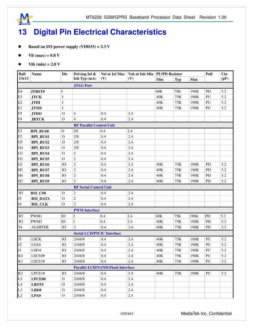
MT6226 GSM/GPRS Baseband Processor Data Sheet Revision 1.00
459/463 MediaTek Inc. Confidential
13 Digital Pin Electrical Characteristics
Based on I/O power supply (VDD33) = 3.3 V
Vil (max) = 0.8 V
Vih (min) = 2.0 V
PU/PD Resistor Ball 13x13
Name Dir Driving Iol & Ioh Typ (mA)
Vol at Iol Max (V)
Voh at Ioh Min (V) Min Typ Max
Pull Cin (pF)
JTAG Port
E4 JTRST# I 40K 75K 190K PD 5.2 E3 JTCK I 40K 75K 190K PU 5.2 E2 JTDI I 40K 75K 190K PU 5.2 E1 JTMS I 40K 75K 190K PU 5.2 F5 JTDO O 4 0.4 2.4 F4 JRTCK O 4 0.4 2.4
RF Parallel Control Unit
F3 BPI_BUS0 O 2/8 0.4 2.4 F2 BPI_BUS1 O 2/8 0.4 2.4 G5 BPI_BUS2 O 2/8 0.4 2.4 G4 BPI_BUS3 O 2/8 0.4 2.4 G3 BPI_BUS4 O 2 0.4 2.4 G2 BPI_BUS5 O 2 0.4 2.4 G1 BPI_BUS6 IO 2 0.4 2.4 40K 75K 190K PD 5.2 H5 BPI_BUS7 IO 2 0.4 2.4 40K 75K 190K PD 5.2 H4 BPI_BUS8 IO 2 0.4 2.4 40K 75K 190K PD 5.2 H3 BPI_BUS9 IO 2 0.4 2.4 40K 75K 190K PD 5.2
RF Serial Control Unit
H1 BSI_CS0 O 2 0.4 2.4 J5 BSI_DATA O 2 0.4 2.4 J4 BSI_CLK O 2 0.4 2.4
PWM Interface
R3 PWM1 IO 2 0.4 2.4 40K 75K 190K PD 5.2 R2 PWM2 IO 2 0.4 2.4 40K 75K 190K PD 5.2 T4 ALERTER IO 2 0.4 2.4 40K 75K 190K PD 5.2
Serial LCD/PM IC Interface
J3 LSCK IO 2/4/6/8 0.4 2.4 40K 75K 190K PU 5.2 J2 LSA0 IO 2/4/6/8 0.4 2.4 40K 75K 190K PU 5.2 J1 LSDA IO 2/4/6/8 0.4 2.4 40K 75K 190K PU 5.2 K4 LSCE0# IO 2/4/6/8 0.4 2.4 40K 75K 190K PU 5.2 K3 LSCE1# IO 2/4/6/8 0.4 2.4 40K 75K 190K PU 5.2
Parallel LCD/NAND-Flash Interface
K2 LPCE1# IO 2/4/6/8 0.4 2.4 40K 75K 190K PU 5.2 L5 LPCE0# O 2/4/6/8 0.4 2.4 L4 LRST# O 2/4/6/8 0.4 2.4 L3 LRD# O 2/4/6/8 0.4 2.4 L2 LPA0 O 2/4/6/8 0.4 2.4

MT6226 GSM/GPRS Baseband Processor Data Sheet Revision 1.00
460/463 MediaTek Inc. Confidential
L1 LWR# O 2/4/6/8 0.4 2.4 F6 NLD17 IO 2/4/6/8 0.4 2.4 40K 75K 190K PD 5.2 G6 NLD16 IO 2/4/6/8 0.4 2.4 40K 75K 190K PD 5.2 L11 NLD15 IO 2/4/6/8 0.4 2.4 40K 75K 190K PD 5.2 L10 NLD14 IO 2/4/6/8 0.4 2.4 40K 75K 190K PD 5.2 L9 NDL13 IO 2/4/6/8 0.4 2.4 40K 75K 190K PD 5.2 K11 NLD12 IO 2/4/6/8 0.4 2.4 40K 75K 190K PD 5.2 K9 NLD11 IO 2/4/6/8 0.4 2.4 40K 75K 190K PD 5.2 J11 NLD10 IO 2/4/6/8 0.4 2.4 40K 75K 190K PD 5.2 J10 NLD9 IO 2/4/6/8 0.4 2.4 40K 75K 190K PD 5.2 J9 NLD8 IO 2/4/6/8 0.4 2.4 40K 75K 190K PD 5.2 M5 NLD7 IO 2/4/6/8 0.4 2.4 40K 75K 190K PD 5.2 M4 NLD6 IO 2/4/6/8 0.4 2.4 40K 75K 190K PD 5.2 M3 NLD5 IO 2/4/6/8 0.4 2.4 40K 75K 190K PD 5.2 N5 NLD4 IO 2/4/6/8 0.4 2.4 40K 75K 190K PD 5.2 N4 NLD3 IO 2/4/6/8 0.4 2.4 40K 75K 190K PD 5.2 N3 NLD2 IO 2/4/6/8 0.4 2.4 40K 75K 190K PD 5.2 N2 NLD1 IO 2/4/6/8 0.4 2.4 40K 75K 190K PD 5.2 N1 NLD0 IO 2/4/6/8 0.4 2.4 40K 75K 190K PD 5.2 P5 NRNB IO 4 0.4 2.4 40K 75K 190K PU 5.2 P4 NCLE IO 4 0.4 2.4 40K 75K 190K PD 5.2 P3 NALE IO 4 0.4 2.4 40K 75K 190K PD 5.2 P2 NWE# IO 4 0.4 2.4 40K 75K 190K PU 5.2 P1 NRE# IO 4 0.4 2.4 40K 75K 190K PU 5.2 R4 NCE# IO 4 0.4 2.4 40K 75K 190K PU 5.2
SIM Card Interface
L18 SIMRST O 2 0.4 2.4 L17 SIMCLK O 2 0.4 2.4 K15 SIMVCC O 2 0.4 2.4 K16 SIMSEL IO 2 0.4 2.4 40K 75K 190K PD 5.2 K17 SIMDATA IO 2 0.4 2.4 5.2
Dedicated GPIO Interface
U2 GPIO0 IO 2 0.4 2.4 40K 75K 190K PD 5.2 M19 GPIO1 IO 2 0.4 2.4 40K 75K 190K PD 5.2 L15 GPIO2 IO 2 0.4 2.4 40K 75K 190K PU 5.2 L16 GPIO3 IO 2 0.4 2.4 40K 75K 190K PU 5.2 C17 GPIO4 IO 4 0.4 2.4 5.2 A19 GPIO5 IO 4 0.4 2.4 5.2 B18 GPIO6 IO 4 0.4 2.4 5.2 B17 GPIO7 IO 4 0.4 2.4 5.2 A18 GPIO8 IO 4 0.4 2.4 5.2 A17 GPIO9 IO 4 0.4 2.4 5.2
Miscellaneous
U1 SYSRST# I 5.2 R18 WATCHDOG# O 4 0.4 2.4 T3 SRCLKENAN O 2 0.4 2.4 T1 SRCLKENA O 2 0.4 2.4 T2 SRCLKENAI IO 2 0.4 2.4 40K 75K 190K PD 5.2

MT6226 GSM/GPRS Baseband Processor Data Sheet Revision 1.00
461/463 MediaTek Inc. Confidential
Keypad Interface
G17 KCOL6 I 2 40K 75K 190K PU 5.2 G18 KCOL5 I 2 40K 75K 190K PU 5.2 G19 KCOL4 I 2 40K 75K 190K PU 5.2 F15 KCOL3 I 2 40K 75K 190K PU 5.2 F16 KCOL2 I 2 40K 75K 190K PU 5.2 F17 KCOL1 I 2 40K 75K 190K PU 5.2 F18 KCOL0 I 2 40K 75K 190K PU 5.2 F19 KROW5 O 2/8 0.4 2.4 E16 KROW4 O 2/8 0.4 2.4 E17 KROW3 O 2/8 0.4 2.4 E18 KROW2 O 2/8 0.4 2.4 D16 KROW1 O 2 0.4 2.4 D19 KROW0 O 2 0.4 2.4
External Interrupt Interface
V1 EINT0 I 40K 75K 190K PU 5.2 U3 EINT1 I 40K 75K 190K PU 5.2 W1 EINT2 I 40K 75K 190K PU 5.2 V2 EINT3 I 40K 75K 190K PU 5.2 R5 MIRQ I 4 0.4 2.4 40K 75K 190K PU 5.2 R17 MFIQ I 2 0.4 2.4 40K 75K 190K PU 5.2
External Memory Interface
R16 ED0 IO 2~16 0.4 2.4 5.2 R15 ED1 IO 2~16 0.4 2.4 5.2 T19 ED2 IO 2~16 0.4 2.4 5.2 T17 ED3 IO 2~16 0.4 2.4 5.2 U19 ED4 IO 2~16 0.4 2.4 5.2 U18 ED5 IO 2~16 0.4 2.4 5.2 V18 ED6 IO 2~16 0.4 2.4 5.2 W19 ED7 IO 2~16 0.4 2.4 5.2 U17 ED8 IO 2~16 0.4 2.4 5.2 V17 ED9 IO 2~16 0.4 2.4 5.2 W17 ED10 IO 2~16 0.4 2.4 5.2 T16 ED11 IO 2~16 0.4 2.4 5.2 W16 ED12 IO 2~16 0.4 2.4 5.2 T15 ED13 IO 2~16 0.4 2.4 5.2 U15 ED14 IO 2~16 0.4 2.4 5.2 V15 ED15 IO 2~16 0.4 2.4 5.2 U14 ERD# O 2~16 0.4 2.4 W14 EWR# O 2~16 0.4 2.4 R13 ECS0# O 2~16 0.4 2.4 T13 ECS1# O 2~16 0.4 2.4 U13 ECS2# O 2~16 0.4 2.4 V13 ECS3# O 2~16 0.4 2.4 R12 ECS4# O 2~16 0.4 2.4 T12 ECS5# O 2~16 0.4 2.4 U12 ECS6# O 2~16 0.4 2.4 W12 ECS7# O 2~16 0.4 2.4 R14 ELB# O 2~16 0.4 2.4

MT6226 GSM/GPRS Baseband Processor Data Sheet Revision 1.00
462/463 MediaTek Inc. Confidential
T14 EUB# O 2~16 0.4 2.4 T11 EPDN# O 2 0.4 2.4 U11 EADV# O 2~16 0.4 2.4 R11 EWAIT O 2~16 40K 75K 190K PU V11 ECLK O 2~16 0.4 2.4 R10 EA0 O 2~16 0.4 2.4 T10 EA1 O 2~16 0.4 2.4 U10 EA2 O 2~16 0.4 2.4 W10 EA3 O 2~16 0.4 2.4 T9 EA4 O 2~16 0.4 2.4 U9 EA5 O 2~16 0.4 2.4 V9 EA6 O 2~16 0.4 2.4 R8 EA7 O 2~16 0.4 2.4 T8 EA8 O 2~16 0.4 2.4 W8 EA9 O 2~16 0.4 2.4 R7 EA10 O 2~16 0.4 2.4 T7 EA11 O 2~16 0.4 2.4 U7 EA12 O 2~16 0.4 2.4 V7 EA13 O 2~16 0.4 2.4 R6 EA14 O 2~16 0.4 2.4 T6 EA15 O 2~16 0.4 2.4 U6 EA16 O 2~16 0.4 2.4 W6 EA17 O 2~16 0.4 2.4 T5 EA18 O 2~16 0.4 2.4 U5 EA19 O 2~16 0.4 2.4 V5 EA20 O 2~16 0.4 2.4 W5 EA21 O 2~16 0.4 2.4 V4 EA22 O 2~16 0.4 2.4 U4 EA23 O 2~16 0.4 2.4 W3 EA24 O 2~16 0.4 2.4 W2 EA25 O 2~16 0.4 2.4
P19 MCCM0 IO 2~16 0.4 2.4 40K 75K 190K PU/PD 5.2 N15 MCDA0 IO 2~16 0.4 2.4 40K 75K 190K PU/PD 5.2 N16 MCDA1 IO 2~16 0.4 2.4 40K 75K 190K PU/PD 5.2 N17 MCDA2 IO 2~16 0.4 2.4 40K 75K 190K PU/PD 5.2 N18 MCDA3 IO 2~16 0.4 2.4 40K 75K 190K PU/PD 5.2 M18 MCCK O 2~16 0.4 2.4 N19 MCPWRON O 2 0.4 2.4 M16 MCWP I 2 40K 75K 190K PU/PD 5.2 M17 MCINS I 2 40K 75K 190K PU/PD 5.2
UART/IrDA Interface
K18 URXD1 I 2 40K 75K 190K PU 5.2 K19 UTXD1 O 2 0.4 2.4 J16 UCTS1 I 2 40K 75K 190K PU 5.2 J17 URTS1 O 2 0.4 2.4 J18 URXD2 IO 2 0.4 2.4 40K 75K 190K PU 5.2 J19 UTXD2 IO 2 0.4 2.4 40K 75K 190K PU 5.2 H15 URXD3 IO 2 0.4 2.4 40K 75K 190K PU 5.2

MT6226 GSM/GPRS Baseband Processor Data Sheet Revision 1.00
463/463 MediaTek Inc. Confidential
H16 UTXD3 IO 2 0.4 2.4 40K 75K 190K PU 5.2 H17 IRDA_RXD IO 2 0.4 2.4 40K 75K 190K PU 5.2 G15 IRDA_TXD IO 2 0.4 2.4 40K 75K 190K PU 5.2 G16 IRDA_PDN IO 2 0.4 2.4 40K 75K 190K PU 5.2
Digital Audio Interface
D17 DAICLK IO 4 0.4 2.4 40K 75K 190K PU 5.2 D18 DAIPCMOUT IO 4 0.4 2.4 40K 75K 190K PD 5.2 C19 DAIPCMIN IO 4 0.4 2.4 40K 75K 190K PU 5.2 C18 DAIRST IO 4 0.4 2.4 40K 75K 190K PU 5.2 B19 DAISYNC IO 2/4/6/8 0.4 2.4 40K 75K 190K PU 5.2
Image Sensor Interface
J12 CMRST IO 2 0.4 2.4 40K 75K 190K PD 5.2 K12 CMPDN IO 2 0.4 2.4 40K 75K 190K PD 5.2 H12 CMVREF I 2 40K 75K 190K PD 5.2 H11 CMHREF I 2 40K 75K 190K PD 5.2 H9 CMPCLK I 2 40K 75K 190K PD 5.2 H10 CMMCLK O 2/4/6/8 0.4 2.4 H8 CMDAT9 I 2/4/6/8 0.4 2.4 40K 75K 190K PD 5.2 J8 CMDAT8 I 2/4/6/8 0.4 2.4 40K 75K 190K PD 5.2 K8 CMDAT7 I 2/4/6/8 0.4 2.4 40K 75K 190K PD 5.2 L8 CMDAT6 I 2/4/6/8 0.4 2.4 40K 75K 190K PD 5.2 M8 CMDAT5 I 2/4/6/8 0.4 2.4 40K 75K 190K PD 5.2 M9 CMDAT4 I 2/4/6/8 0.4 2.4 40K 75K 190K PD 5.2 M10 CMDAT3 I 2/4/6/8 0.4 2.4 40K 75K 190K PD 5.2 M11 CMDAT2 I 2/4/6/8 0.4 2.4 40K 75K 190K PD 5.2 M12 CMDAT1 IO 2/4/6/8 0.4 2.4 40K 75K 190K PD 5.2 L12 CMDAT0 IO 2/4/6/8 0.4 2.4 40K 75K 190K PD 5.2