Embed Size (px)
Citation preview

MPMC UNIT 1 SIETK
1 | P a g e
Syllabus: UNIT- I Introduction to microprocessors - 8085 Architecture-Block Diagram, Flag Register,
Pin Diagram, Timing and Control Signals, System Timing Diagram, Instruction Set of 8085- Instruction
& Data Formats- Addressing Modes- Instructions.
INTRODUCTION TO MICROPROCESSORS
Microprocessor:
Programmable integrated device that has computing ability and decision-making capacity. It is the CPU of a computer. A multipurpose, programmable, clock driver, register based electronic device that reads binary instruction from memory, accepts binary data, processes the data according to the instruction and provides the results as output. A controlled intelligent device(processor). Human analogy of a computer:
CPU = brain Bus = nerves Input device = Eyes and ears Output device =Mouth and hands storage = Memory
Basics of Computer Terminology:
Bit – Binary Digits(0 and 1) Nibble-combination of 4 bits byte –combination of 8 bits System-Set of devices used to perform a task Hardware-Physical components of a system Software-set of programs. Program-set of instruction used to perform a task. Instruction-command to the microprocessor to perform a task. Mnemonics-abbreviation for each binary instruction word. Bus-communication path usually set of wires. Word length: The number of bits that can be processed by a microprocessor is termed as word length of the microprocessor. Word length of 8085 is 8 bits. C, C++, Java, Python etc – High level languages Assembly Language - low level language. Machine Language - very low level programming language
- Combination of 0’s and 1’s. - Only processor understandable.
Assembler – Converts Assembly language to machine language. Compiler- Converts High level language to machine language. History of Evolution of Microprocessors The microprocessor is nothing but the CPU and it is an essential component of the computer. It is a
silicon chip that comprises millions of transistors and other electronic components that process
millions of instructions per second. A Microprocessor is a versatile chip, that is combined with memory
and special purpose chips and preprogramed by a software. It accepts digital data as i/p and processes
it according to the instructions stored in the memory. The microprocessor has many functions like

MPMC UNIT 1 SIETK
2 | P a g e
functions of data storage, interact with various other devices and other time related functions. But,
the main function is to send and receive the data to make the function of the computer well.
The microprocessor has become more essential part of many gadgets. The evolution of
microprocessors was divided into five generations such as first, second, third, fourth and fifth
generation and the characteristics of these generations are discussed below.
First Generation Microprocessors
The first generation microprocessors were introduced in the year 1971-1972. The instructions of these
microprocessors were processed serially, they fetched the instruction, decoded and then executed it.
When an instruction of the microprocessor was finished, then the microprocessor updates the
instruction pointer & fetched the following instruction, performing this consecutive operation for each
instruction in turn.
Second Generation Microprocessors
In the year 1970, small amount of transistors were available on the integrated circuit in the second
generation microprocessors. Examples of the second generation microprocessors are 16-bit
arithmetic 7 pipelined instruction processing, MC68000 Motorola microprocessor. These processors
are introduced in the year 1979, and Intel 8080 processor is another example of the microprocessor.
The second generation of the microprocessor is defined by overlapped fetch, decode and execute the
steps. When the first generation is processed in the execution unit, then the second instruction is
decoded and the third instruction is fetched.
The difference between the first generation microprocessor and second generation microprocessors
was mainly the use of new semiconductor technologies to manufacture the chips. The result of this
technology resulted in a fivefold increase in instruction, speed, execution and higher chip densities.
Third Generation Microprocessors
The third generation microprocessors were introduced in the year 1978, as denoted by Intel’s 8086
and the Zilog Z8000. These were 16-bit processors with a performance like mini computers. These
types of microprocessors were different from the previous generations of microprocessors in that all
main workstation industrialists began evolving their own ISC based microprocessor architectures.
Fourth Generation Microprocessors
As many industries converted from commercial microprocessors to in house designs, the fourth
generation microprocessors are entered with outstanding design with a million transistors. Leading
edge microprocessors like Motorola’s 88100 and Intel’s 80960CA could issue & retire more than one
instruction per clock cycle.
Fifth Generation Microprocessors
Fifth generation microprocessors employed decoupled super scalar processing, and their design soon
exceeded 10 million transistors. In fifth generation, PCs are a low-margin, high volume business
conquered by a single microprocessor.
Microprocessors are categorized based on its size:
Transistor was invented in 1948 (23 December 1947 in Bell lab). IC was invented in 1958 (Fair Child
Semiconductors) By Texas Instruments J kilby. First microprocessor was invented by INTEL(INTegrated
ELectronics).

MPMC UNIT 1 SIETK
3 | P a g e
Size of microprocessor – 4 bit
NAME YEAR OF INVENTION
CLOCK
SPEED
NUMBER OF
TRANSISTORS
INST. PER
SEC
INTEL
4004/4040
1971 by Ted Hoff and
Stanley Mazor 740 KHz 2300 60,000
Size of microprocessor – 8 bit
NAME YEAR OF INVENTION
CLOCK
SPEED
NUMBER OF
TRANSISTORS INST. PER SEC
8008 1972 500 KHz
50,000
8080 1974 2 MHz 60,000
10 times faster than
8008
8085
1976 (16 bit address
bus) 3 MHz 6500 769230
Size of microprocessor – 16 bit
NAME YEAR OF INVENTION
CLOCK
SPEED
NUMBER OF
TRANSISTORS
INST. PER
SEC
8086
1978 (multiply and divide instruction,
16 bit data bus and 20 bit address bus)
4.77
MHz, 8
MHz, 10
MHz 29000
2.5
Million
8088
1979 (cheaper version of 8086 and 8 bit
external bus)
2.5
Million
80186/80188
1982 (80188 cheaper version of 80186,
and addtional components like
interuppt controller, clock generator,
local bus controller,counters) 6 MHz
80286
1982 (data bus 16bit and address bus
24 bit) 8 MHz 134000
4
Million

MPMC UNIT 1 SIETK
4 | P a g e
Size of microprocessor – 32 bit
NAME YEAR OF INVENTION
CLOCK
SPEED
NUMBER OF
TRANSISTORS INST. PER SEC
INTEL
80386
1986 (other versions
80386DX, 80386SX, 80386SL
and data bus 32 bit address
bus 32 bit)
16 MHz
– 33
MHz 275000
INTEL
80486
1986 (other versions
80486DX, 80486SX,
80486DX2, 80486DX4)
16 MHz
– 100
MHz
1.2 Million
transistors
8 KB of cache
memory
PENTIUM 1993 66 MHz
Cache memory 8 bit
for instructions 8 bit
for data
Size of microprocessor – 64 bit
NAME YEAR OF INVENTION CLOCK SPEED
NUMBER OF
TRANSISTORS INST. PER SEC
INTEL
core 2
2006 (other versions
core2 duo, core2 quad,
core2 extreme) 1.2 GHz to 3 GHz
291 Million
transistors
64 KB of L1
cache per core
4 MB of L2
cache
i3, i5,
i7 2007, 2009, 2010
2.2GHz – 3.3GHz,
2.4GHz – 3.6GHz,
2.93GHz – 3.33GHz

MPMC UNIT 1 SIETK
5 | P a g e
Intel 8085 Microprocessor: 8085 is pronounced as "eighty-eighty-five" microprocessor.
It is an 8-bit microprocessor designed by Intel in 1976 using NMOS technology.
The features of 8085 include:
1. It is an 8-bit microprocessor i.e. it can accept, process or provide 8-bit data simultaneously. 2. It operates on a single +5V power supply connected at Vcc 3. It operates on clock cycle with 50% duly cycle. 4. It has on chip clock generator this internal clock generator requires tuned circuit like LC, RC or crystal. The internal clock generator divides oscillation frequency by 2 and generates clock signal, which can be used for synchronizing external devices. 5. It can operate with 3 MHz clock frequency. 6. It has 16 address buses, hence it can access 216 = 64Kbytes of memory. 7. It provides 8 bit I/o address to acce4ss (28) 256 I / o ports. 8. In 8085, the lower 8-bit address bus (A0-A7) and data bus (D0-D7) are multiplexed to reduce number of external pins. But due to this, external hardware is required to separate address lines and data lines. 9. It supports 74 instructions (Mnemonics) with following addressing modes. (a) Immediate, (b) Register, (c) Direct (d) Indirect (e) Implied. 10. The Arithmetic logic unit of 8085 performs a) 8 bit binary addition with or without carry. (b) 16 bit binary addition (c) 2 digit BCD addition (d) 8-bit binary subtraction with or without borrow (e) 8-bit logical AND, OR, EX-OR, complement (NOT) and bit shift operations. 11. It has 8-bit accumulator, flag register, instruction, register, six 8-bit general purpose Registers (B, C, D, E, H and C) and five 16-bit registers (SP and PC) 12. It provides five hardware interrupts: TRAP, RST 7.5. RST 6.5, RST 5.5 and INTR. 13. It has serial I/O control which allows serial communication. 14. It provides control signals (IO /M, RD, WR) to control bus cycles. 15. The external hardware (another microprocessor or equivalent master) can detect which machine cycle microprocessor is executing using status signals (IO/M, S0, S1) This feature is useful when more than one processors are using common system resources (memory & I/O devices). 16. It has mechanism by which it is possible to increase its interrupt handling capacity. 17. The 8085 has an ability to share system bus with direct memory access controller. This feature allows to transfer large amount of data from I/O device to memory or from memory to I/O device with high speeds.
ARCHITECTURE OF 8085
It consists of various functions blocks as listed below: 1) Registers 2) Arithmetic and logic unit 3) Instruction decoder and machine cycle encoder 4) Address Buffer 5) Address / Data Buffer 6) Incrementor / Decrementor address batch 7) Serial I/O control 8) Timing and control circuitry

MPMC UNIT 1 SIETK
6 | P a g e
REGISTERS: It has eight addressable 8-bit registers: A, B, C, D, E, H, L, F and two 16-bit registers PC and SP. These register can be classified as : 1. General purpose registers 2. Temporary registers (a) Temporary data register (b) W and Z registers 3. Special purpose registers (a) Accumulator (b) Flag registers (c) Instruction register 4. Sixteen bit registers (a) Program counter PC (b) Stack pointer (SP)
Figure -Architecture of 8085
Registers in 8085
ALU

MPMC UNIT 1 SIETK
7 | P a g e
1. General Purpose Registers : B,C,D,E,H and L are 8-bit general purpose registers can be used as a separate 8-bit registers or as 16-bit register pairs, BC,DE and HL. HL pair also functions as a data pointer or memory pointer. These are also called Scratch pad registers, as user can store data in them. To store and read data from these registers bus access is not required, it is an internal operation. Thus it provides an efficient way to store intermediate results and used them when required. 2. Temporary Registers : a) Temporary Data Register : The ALU has two inputs. One input is supplied by the accumulator and other from temporary data register. The programmer cannot access this temporary data register. However, it is internally used for execution of most arithmetic and logical instructions. b) W and Z registers : W and Z registers are temporary registers. These registers are used to hold 8-bit data during execution of some instruments. These registers are not available for programmer, since 8085 user them internally. 3. Special Purpose Registers: a) Register A (Accumulator) : It is a tri-state eight bit register it is extensively used in arithmetic, logic, load and store operations, as well as, input / output (I/O) operations. Most of the times the result of arithmetic and logical operations is stored in the register A, hence it is also identified as accumulator. b) Flag Register : It is an 8-bit register, in which five of the bits carry significant information in the form of flags: S (sign flag) Z (Zero flag), AC (Auxillary carry flag)m P (Parity flag) and CY (carry flag).
Figure -Flag Register
S-Sign flag: After the execution of arithmetic or logic operation, if bit D7 of the result is 1, the sign flag is set. In a given byte if bit D7 is 1, the number will be viewed as negative number. If D7 is 0, the number is considered as positive number. Z-Zero flag: The zero flag sets if the result of operation in ALU is zero and flag resets if result is non zero. The zero flag is also set if a certain register content becomes zero following an increment or decrement operation of that register. AC-Auxiliary carry flag: This flag is set if there is an overflow out of bit3 i.e., carry from lower nibble to higher nibble (D3 to D4 bit). This flag is used for BCD operations. P-Parity flag: Parity is defined by the number of ones present in the accumulator. After an arithmetic or logic operation if the result has an even number of ones, i.e., even parity, the flag is set. If the parity is odd, flag is reset. CY-Carry flag: This flag is set, if there is an overflow out of bit 7. The carry flag also serves as a borrow flag for subtraction. c) Instruction register: In a typical processor operation, the processor first fetches the opcode of instruction from memory (i.e. it places an address on the address bus and memory responds by placing the

MPMC UNIT 1 SIETK
8 | P a g e
data stored at the specified address on the data bus). The CPU stores this opcode in a register called instruction register. This opcode is further sent to the instruction decoder to select one of the alternatives. 4.Sixteen bit registers a) Program Counter (PC): Program is a sequence of instructions. Microprocessor fetches these instructions from the memory and executes them sequentially. The program counter is a special purpose register which, at a given time, stores the address of the next instruction to be fetched. Program counter acts as a pointer to the next instruction. How processor increments the program counter depends upon the nature of instructions: for one byte instruction it increments program counter by one, for two byte instruction it increments program counter by two and for three byte instruction it increments program counter by three such that program counter always points to the address of the next instruction. b) Stack Pointer: The stack is a reserved area of the memory in the RAM where temporary information may be stored. A 16-bit stack pointer is used to hold the address of the most recent stack entry. Arithmetic and Logic Unit (ALU): The 8085’s ALU performs arithmetic and logical functions on eight bit variables. The arithmetic unit performs bitwise fundamental, operation such as addition and subtraction. The logic unit performs the logical operations such as complement, AND, OR and EX-OR as well as rotate and clear. The ALU also looks after branching decisions. Instruction Decoder The processor first fetches the opcode of instruction from memory and stores this opcode in the instruction register. It is then sent to the instruction decoder. The instruction decoder decodes it and accordingly gives the timing and control signals which control the register, data buffer, ALU, and external peripheral signals. The 8085 executes seven different types of machine cycles. It gives the information about which machine cycle is currently executing in the encoded form on the S0, S1 and IO/M lines. The task is done by machine cycle encoder. Address buffer This is an 8-bit unidirectional buffer. It is used to drive external high order address (A15-A8). It is also used to tri-state the high order address bus under certain conditions such as reset, hold, halt and when address lines are not in use. Address / Data buffer This is an 8-bit bidirectional buffer. It is used to drive multiplexed address/data bus i.e. low order address bus (A7-A0) and data bus (D7-D0). It is also used to tri-state the multiplexed address/data bus under certain conditions such as reset, hold, halt and when bus is not in use. Incrementer/Decrementer address latch This 16-bit register is used to increment or decrement the contents of program counter or stack pointer as a part of execution of instructions related to them.

MPMC UNIT 1 SIETK
9 | P a g e
Interrupt Control The processor fetches, decodes and executes the instructions in a sequence. Sometimes it is necessary to have the processor automatically execute one of a collection of special routines whenever special condition exists within a program or the microcomputer system. After the execution of special routine, the program control must be transferred to the program which processor was executing before the occurrence of the special condition. The occurrence of this special condition is referred as interrupt. The interrupt control block has five interrupt inputs RST 5.5, RST 6.5, RST 7.5, TRAP and INTR and one acknowledge signal INTA. Serial I/O Control In situations like, data transmission over long distance and communication with cassette tapes or CRT terminal, it is necessary to transmit data bit by bit to reduce the cost of cabling. In serial communication one bit is transferred at a time over a single line. The 8085’s serial I/O control provides two lines, SID and SOD for serial communication. The Serial Output Data (SOD) line is used to send data serially and Serial Input Data (SID) line is used to receive data serially. Timing and Control circuitry The control circuitry in the processor 8085 is responsible for all the operations. The control circuitry and hence the operations in 8085 are synchronized with the help of clock signal. Along with the control of fetching and decoding operations and generating appropriate signals for instruction execution, control circuitry, also generates signals required to interface external devices to the processor 8085.
PIN DIAGRAM OF 8085 The signals of 8085 can be classified into six groups according to their functions: a) Address bus b) Data bus c) Control and status signals d) Power supply and frequency signals e) Externally initiated signals and f) Serial I/O ports. ADDRESS BUS The 8085 has eight lines, A15-A8, which are unidirectional and used as the high order address bus. MULTIPLEXED ADDRESS / DATA BUS The signal lines AD7-AD0 are bidirectional: they serve a dual purpose. They are used as the low order address bus as well as the data bus. In executing an instruction, during the earlier part of the cycle, these lines are used as the low-order address bus. During the later part of the cycle, these lines are used as the data bus. (This is also known as multiplexing the bus.) However, the low-order address bus can be separated from these signals by using a latch.

MPMC UNIT 1 SIETK
10 | P a g e
Figure Pin diagram of 8085
CONTROL AND STATUS SIGNALS This group of signals includes two control signals (RD and WR), three status signals (IO/M, S1, and S0) to identify the nature of the operation, and one special signal (ALE) to indicate the beginning of the operation. These signals are as follows:
• ALE — Address Latch Enable: This is positive going pulse generated every time the 8085 begins an operation (machine cycle); it indicates that the bits on AD7-AD0 are address bits. This is used primarily to latch the low-order address from the multiplexed bus and generate a separate set of eight address lines, A7-A0.
• RD¯ — Read: This read control signal (active low). This signal indicates that the selected I/O or memory device is to be read and data are available on the data bus.
• WR¯ — Write: This is a write control signal (active low). This signal indicates that the data on the data bus are to be written on into a selected memory device or I/O location.
• IO/M¯ : This is status signal used to differentiate between I/O and memory operations. When it is high, it indicates an I/O operation; when it is low, it indicates a memory operation. This signal combines with RD and WR to generate I/O and memory control signals.
• S1 and S0: These status signals, similar to IO/M, can identify various operations, but they are rarely used in small systems.

MPMC UNIT 1 SIETK
11 | P a g e
POWER SUPPLY AND CLOCK FREQUENCY The power supply and frequency signals are as follows:
• Vcc: +5V power supply.Vss: Ground reference.
• X1, X2: A crystal is connected at these two pins. The frequency is internally divided by two; therefore, to operate a system at 3MHz and, the crystal should have frequency of 6MHz.
• CLK (OUT) — Clock out: This signal is used as the system clock for other devices. EXTERNALLY INITIATED SIGNALS, INCLUDING INTERRUPTS The 8085 has five interrupt signals that can be used to interrupt a program execution. The interrupt signals are Interrupt Request (INTR), Restart Interrupts (RST5.5, RST 6.5, RST7.5) and TRAP. The microprocessor acknowledges an interrupt request by the INTA (Interrupt acknowledge) signal. In addition to the interrupts, three pins — RESET, HOLD, and READY accept the externally initiated signals as inputs. To respond to the HOLD request, the 8085 has one signal called HLDA (Hold Acknowledge). RESET, HOLD and READY are additional interrupts. They accept the externally initiated signals as inputs. To respond to the HOLD request, it has one signal called HLDA. RESET IN: When the signal on this pin goes low, the program counter is set to zero, the buses are tri-stated, and the microprocessor is reset. RESET OUT: This signal indicates that the microprocessor is being reset. The signal can be used to reset other devices.
MPMC UNIT 1 SIETK
12 | P a g e
SERIAL I/O PORTS The microprocessor has 2 pins specially designed for software –controlled serial I/O. one is called SOD (Serial Output Data) and the other is called SID (Serial Input Data). Data transfer is controlled through 2 instructions: SIM and RIM. The instruction SIM is necessary to output data serially from the SOD line. Similarly instruction RIM is used to input serial data through the SID line. The SID and SOD lines in the 8085 eliminate the need for an input port and an output port in the software-controlled serial I/O. Essentially, the SID is a 1-bit port and SOD is a 1- bit output port.
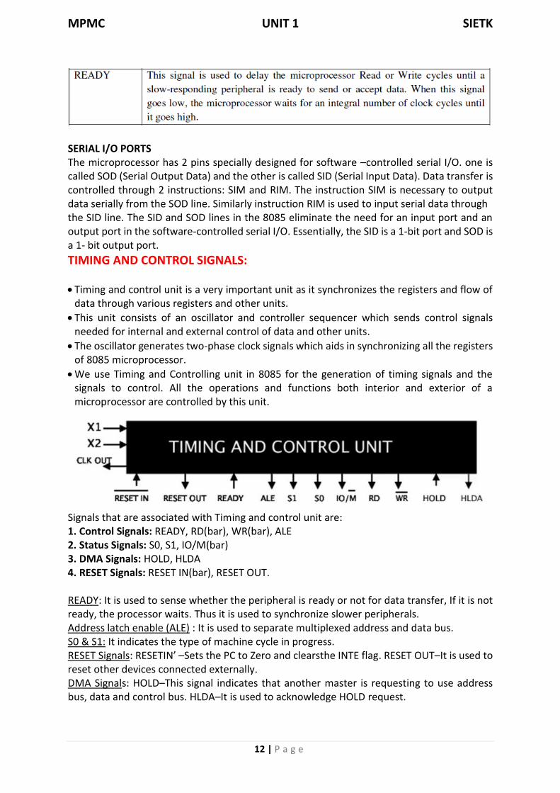
TIMING AND CONTROL SIGNALS:
• Timing and control unit is a very important unit as it synchronizes the registers and flow of data through various registers and other units.
• This unit consists of an oscillator and controller sequencer which sends control signals needed for internal and external control of data and other units.
• The oscillator generates two-phase clock signals which aids in synchronizing all the registers of 8085 microprocessor.
• We use Timing and Controlling unit in 8085 for the generation of timing signals and the signals to control. All the operations and functions both interior and exterior of a microprocessor are controlled by this unit.
Signals that are associated with Timing and control unit are: 1. Control Signals: READY, RD(bar), WR(bar), ALE 2. Status Signals: S0, S1, IO/M(bar) 3. DMA Signals: HOLD, HLDA 4. RESET Signals: RESET IN(bar), RESET OUT. READY: It is used to sense whether the peripheral is ready or not for data transfer, If it is not ready, the processor waits. Thus it is used to synchronize slower peripherals. Address latch enable (ALE) : It is used to separate multiplexed address and data bus. S0 & S1: It indicates the type of machine cycle in progress. RESET Signals: RESETIN’ –Sets the PC to Zero and clearsthe INTE flag. RESET OUT–It is used to reset other devices connected externally. DMA Signals: HOLD–This signal indicates that another master is requesting to use address bus, data and control bus. HLDA–It is used to acknowledge HOLD request.

MPMC UNIT 1 SIETK
13 | P a g e
RD’ –Read (active low). To indicate that the I/O or memory selected is to be read and data are available on the bus. WR’ –Write( Active low). This is to indicate that the data available on the bus are to be written to memory or I/O ports. IO/M’ –To differentiate I/O operation of memory operations. –‘0’ - indicates a memory operation. –‘1’-indicates an I/O operation. IO/M’ combined with RD’ and WR’ to generate I/O and memory control signals.
SYSTEM TIMING DIAGRAM Instruction Cycle: The time required to execute an instruction is called instruction cycle. Machine Cycle: The time required to access the memory or input/output devices is called machine cycle. T-State:
• The machine cycle and instruction cycle takes multiple clock periods.
• A portion of an operation carried out in one system clock period is called as T-state. MACHINE CYCLES OF 8085: The 8085 microprocessor has 5 (seven) basic machine cycles. They are 1. Opcode fetch cycle (4T) 2. Memory read cycle (3 T) 3. Memory write cycle (3 T) 4. I/O read cycle (3 T)

MPMC UNIT 1 SIETK
14 | P a g e
5. I/O write cycle (3 T)
• Each instruction of the 8085 processor consists of one to five machine cycles, i.e., when the 8085 processor executes an instruction, it will execute some of the machine cycles in a specific order.
• The processor takes a definite time to execute the machine cycles. The time taken by the processor to execute a machine cycle is expressed in T-states.
• One T-state is equal to the time period of the internal clock signal of the processor.
• The T-state starts at the falling edge of a clock.
Opcode fetch machine cycle of 8085 :
• Each instruction of the processor has one byte opcode.
• The opcodes are stored in memory. So, the processor executes the opcode fetch machine cycle to fetch the opcode from memory.
• Hence, every instruction starts with opcode fetch machine cycle.
• The time taken by the processor to execute the opcode fetch cycle is 4T.
• In this time, the first, 3 T-states are used for fetching the opcode from memory and the remaining T-states are used for internal operations by the processor.
Timing Diagram for Opcode Fetch Machine Cycle

MPMC UNIT 1 SIETK
15 | P a g e
Memory Read Machine Cycle of 8085:
• The memory read machine cycle is executed by the processor to read a data byte from memory.
• The processor takes 3T states to execute this cycle.
• The instructions which have more than one byte word size will use the machine cycle after the opcode fetch machine cycle.
Timing Diagram for Memory Read Machine Cycle

MPMC UNIT 1 SIETK
16 | P a g e
Memory Write Machine Cycle of 8085:
• The memory write machine cycle is executed by the processor to write a data byte in a memory location.
• The processor takes, 3T states to execute this machine cycle.
Timing Diagram For Memory Write Machine Cycle
I/O Read Cycle of 8085:
• The I/O Read cycle is executed by the processor to read a data byte from I/O port or from the peripheral, which is I/O, mapped in the system.
• The processor takes 3T states to execute this machine cycle.
• The IN instruction uses this machine cycle during the execution.

MPMC UNIT 1 SIETK
17 | P a g e
Timing Diagram for I/O Read Machine Cycle
I/O Write Cycle of 8085:
• The I/O write machine cycle is executed by the processor to write a data byte in the I/O port or to a peripheral, which is I/O, mapped in the system.
• The processor takes, 3T states to execute this machine cycle.
Timing Diagram for I/O Write Machine Cycle

MPMC UNIT 1 SIETK
18 | P a g e
INSTRUCTION & DATA FORMATS
Instruction Formats: An instruction (instruction format) is a command to the microprocessor to perform a given
task on a particular data. Each instruction (instruction format) is of two parts. One is task to
be performed, called the operation code or opcode and the second one is the data to be
operated on, called the operand. The operands or data can be specified in different ways. It
may include an 8-bit or 16-bit data, an internal register. a memory location, or 8-bit or 16-bit
address. In some instructions, the operand is implicit.
INSTRUCTION WORD SIZE:
The 8085 instruction set is classified into the following three groups according to word size:
1. One-word or 1-byte instructions
2. Two-word or 2-byte instructions
3. Three-word or 3-byte instructions
In the 8085, “byte” and “word” are synonymous because it is an 8-bit microprocessor.
ONE-BYTE INSTRUCTIONS
A one-byte instruction includes a opcode and a operand in the same byte. Operand(s) are
internal registers and are in the instruction in form of codes. If there is no numeral present in
the instruction then that instruction will be of one-byte, for example, MOV C, A, RAL, and ADD
B, etc. Table 1 shows examples of one-byte instruction.
Task Opcode Operand Binary
Code Hex code
Copy the content of accumulator in
the register C. MOV C, A 0100 1111 4FH
Add the contents of register B to
the contents of the accumulator. ADD B 1000 0000 80H
Invert each bit in the accumulator. CMA None 0010 2FH
These instructions are of one-byte performing three different tasks. In the first instruction,
operand and registers are specified. In the second instruction, the operand B is specific and
the accumulator is not there. Similarly, in the third instruction, the accumulator is assume to
be the implicit operand. These instructions are in 8-bit binary format in the memory and each
requires one memory location.
TWO-BYTE INSTRUCTIONS
In a two-byte instruction, the first byte specifies the operation code and second byte specifies
the operand. Source operand is a data byte and immediately following the opcode. If an 8-bit
numeral is present in the instruction then that instruction will be of two-byte. Here, the

MPMC UNIT 1 SIETK
19 | P a g e
numeral may be a data or an address. For example, in MVI A, 35H and IN 29H, etc. In a two-
byte instruction, the first byte will be the opcode and the second byte will be for the numeral
present in the instruction.
Task Opcode Operand Binary
code Hex code
Load an 8-bit data byte
in the accumulator. MVI A 35H
0011 1110
0011 0101
3EH First byte
35H Second byte
This instruction would require two memory locations to store in memory.
THREE-BYTE INSTRUCTIONS
In a three-byte instruction, the first byte specifies the opcode, and the following two bytes
specify the 16-bit operand. The second byte is the low-order operand and the third byte is
the high-order operand. If a 16-bit numeral is present in the instruction then that instruction
will be of three-byte. Here, the numeral may be a data or an address, for example, in LXI
H,3500H and STA 2500H, etc.
Task Opcode Operand Binary
code Hex code
Transfer the program
sequence to the memory
location 2085h
JMP 2550H
1100 0011
0101 0000
0010 0101
C3 First byte
50 Second byte
25 Third byte
This instruction would require three memory locations to store in memory.
Opcode format: The 8085 microprocessor has 8-bit opcodes. The opcode is unique for each Instruction and Data Format of 8085 and contains the information about operation, register to be used, memory to be used etc. The 8085A identifies all operations, registers and flags with a specific code. For example, all internal registers are identified as shown in the Tables 2.1(a) and 2.2(b).

MPMC UNIT 1 SIETK
20 | P a g e
Similarly, there are different codes for each opera are identified as follows :
Data Formats: The operand is an another name for data. It may appear in different forms :
• Addresses
• Numbers/Logical data and
• Characters Addresses : The address is a 16-bit unsigned integer ,number used to refer a memory location. Numbers/Data : The 8085 supports following numeric data types.
• Signed Integer : A signed integer number is either a positive number or a negative number. In 8085, 8-bits are assigned for signed integer, in which most significant bit is used for sign and remaining seven bits are used for Sign bit 0 indicates positive number whereas sign bit 1 indicates negative number.
• Unsigned Integer : The 8085 microprocessor supports 8-bit unsigned integer.
• BCD : The term BCD number stands for binary coded decimal number. It uses ten digits from 0 through 9. The 8-bit register of 8085 can store two digit BCD
Characters : The 8085 uses ASCII code to represent characters. It is a 7-bit alphanumeric code that represents decimal numbers, English alphabets, and other special characters.
ADDRESSING MODES: The different ways that a microprocessor can access data are referred to as addressing modes. The 8085 has 5 addressing modes. These are:
1. Immediate addressing mode 2. Register addressing mode 3. Direct addressing mode 4. Indirect addressing mode 5. Implied addressing mode
1. Immediate addressing mode: In an immediate addressing mode, 8 or 16 bit data can be specified as a part of instruction. In 8085, the instructions having ‘I’ letter fall under this category. “I’ indicates immediate addressing mode. Example: MVI A,20H ; moves 8-bit immediate data(20H) into accumulator. LXI D,10FF H ; moves 16-bit immediate data into DE register pair.

MPMC UNIT 1 SIETK
21 | P a g e
2. Register addressing mode: The register addressing mode specifies the source operand, destination operand or both to be contained in an 8085 registers. This results in faster execution, since it is not necessary to access memory locations for operands. Example: MOV A, B ; moves the contents of register B into the accumulator. SPHL ; moves the contents of HL register pair into stack pointer. 3. Direct addressing mode: The direct addressing mode specifies the 16- bit address of the operand within the instruction itself. The second and third bytes of instruction contain this 16 bit address. Example: LDA 2000H ; loads the 8bit contents of memory location 2000H into the accumulator SHLD 3000H ; Stores the HL register pair into two consecutive memory locations. Lower contents of L register into memory location 3000H and higher contents of H register into memory location 3001H. 4. Indirect addressing mode: In indirect addressing mode, the memory address where the operand located is specified by the contents of a register pair. Example: LDAX B ; loads the accumulator with the contents of memory location pointed by BC register pair. MOV M, A ; Stores the contents of accumulator into the memory location pointed by HL register pair 5. Implied addressing mode: In implied addressing mode, Opcode specifies the address of the operands. Example: CMA; Complements contents of accumulator. RAL; Rotates the contents of accumulator left through the carry.
THE 8085 INSTRUCTION SET
The 8085 instructions can be classified into the following five functional categories: 1. Data transfer (copy) operations 2. Arithmetic operations 3. logical operations 4. Branching operations and 5. Machine control operations. An instruction is a command to the microprocessor to perform a given task on specified data. Each instruction has two parts: one is the task to be performed, called the operation code (opcode), and the second is the data to be operated on, called the operand (or data) can be specified in various ways. It may include 8-bit (or 16-bit) data, an internal register, a memory location, or an 8-bit (or 16-bit) address. 1.DATA TRANSFER (COPY) OPERATIONS This group of instructions copies data from a location called a source to another location called destination, without modifying the contents of the source. The various types of data transfer are listed below together with examples of each type:
• Between registers --- Copy the contents of register B into Register D.

MPMC UNIT 1 SIETK
22 | P a g e
• Specific data byte to a register or a memory -- location Load register B with the data byte
• Between a memory location ---- From the memory location 2000H to and a register register B.
• Between an I/O device and the accumulator --- From an input keyboard to the accumulator.
Opcode Operand Meaning Explanation
MOV Rd, Sc M, Sc Dt, M
Copy from the source (Sc) to the destination(Dt)
This instruction copies the contents of the source register into the destination register without any alteration. Example − MOV D, L
MVI Rd, data M, data
Move immediate 8-bit The 8-bit data is stored in the destination register or memory. Example − MVI B, 55L
LDA 16-bit address
Load the accumulator
The contents of a memory location, specified by a 16-bit address in the operand, are copied to the accumulator. Example − LDA 2034H
LDAX B/D Reg. pair Load the accumulator indirect
The contents of the designated register pair point to a memory location. This instruction copies the contents of that memory location into the accumulator. Example − LDAX D
LXI Reg. pair, 16-bit data
Load the register pair immediate
The instruction loads 16-bit data in the register pair designated in the register or the memory. Example − LXI B, 3225H
LHLD 16-bit address
Load H and L registers direct
The instruction copies the contents of the memory location pointed out by the address into register L and copies the contents of the next memory location into register H. Example − LHLD 3225H
STA 16-bit address
16-bit address
The contents of the accumulator are copied into the memory location specified by the operand. This is a 3-byte instruction, the second byte specifies the low-order address and the third byte specifies the high-order address. Example − STA 3254H

MPMC UNIT 1 SIETK
23 | P a g e
STAX B/D Reg. pair Store the accumulator indirect
The contents of the accumulator are copied into the memory location specified by the Register pair. Example − STAX D
SHLD 16-bit address
Store H and L registers direct
The contents of register L are stored in the memory location specified by the 16-bit address in the operand and the contents of H register are stored into the next memory location by incrementing the operand. This is a 3-byte instruction, the second byte specifies the low-order address and the third byte specifies the high-order address. Example − SHLD 3225H
XCHG None Exchange H and L with D and E
The contents of register H are exchanged with the contents of register D, and the contents of register L are exchanged with the contents of register E. Example − XCHG
SPHL None Copy H and L registers to the stack pointer
The instruction loads the contents of the H and L registers into the stack pointer register. The contents of the H register provide the high-order address and the contents of the L register provide the low-order address. Example − SPHL
XTHL None Exchange H and L with top of stack
The contents of the L register are exchanged with the stack location pointed out by the contents of the stack pointer register. The contents of the H register are exchanged with the next stack location (SP+1). Example − XTHL
OUT 8-bit port address
Output the data from the accumulator to a port with 8bit address
The contents of the accumulator are copied into the I/O port specified by the operand. Example − OUT 80H
IN 8-bit port address
Input data to accumulator from a port with 8-bit address
The contents of the input port designated in the operand are read and loaded into the accumulator. Example – IN 55H
PUSH Reg. pair Push the register pair onto the stack
The contents of the register pair designated in the operand are copied onto the stack in the following sequence.

MPMC UNIT 1 SIETK
24 | P a g e
The stack pointer register is decremented and the contents of the high order register (B, D, H, A) are copied into that location. The stack pointer register is decremented again and the contents of the low-order register (C, E, L, flags) are copied to that location. Example − PUSH K
POP Reg. pair Pop off stack to the register pair
The contents of the memory location pointed out by the stack pointer register are copied to the low-order register (C, E, L, status flags) of the operand. The stack pointer is incremented by 1 and the contents of that memory location are copied to the high-order register (B, D, H, A) of the operand. The stack pointer register is again incremented by 1. Example − POPK
2.ARITHMETIC OPERATIONS These instructions perform arithmetic operations such as addition, subtraction, increment and decrement.
• Addition — Any 8-bit number, or the contents of a register, or the contents of a memory location can be added to the contents of the accumulator and the result is stored in the accumulator. No two other 8-bit registers can be added directly. The instruction DAD is an exception.
• Subtraction — Any 8-bit number, or the contents of a register, or the contents of a memory location can be subtracted from the contents of the accumulator and the result is stored in the accumulator. The subtraction is performed in 2’s complement and the results, if negative, are expressed in 2’s complement. No two other 8-bit registers can be subtracted directly.
• Increment / Decrement — The 8-bit contents of a register or a memory location can be incremented or decremented by one. Similarly, the 16- bit contents of a register pair can be incremented or decremented by 1. These increment and decrement operation differ from the addition and subtraction in an important way; i.e., they can be performed in one of the registers pair in a memory location.
These arithmetic instructions (except INR and DCR) 1. Assume implicitly that the accumulator is one of the operands. 2. Modify all the flags according to the data conditions of the result. 3. place the result in the accumulator 4. Do not affect the contents of the operand register.

MPMC UNIT 1 SIETK
25 | P a g e
The instructions INR and DCR 1. Affect the contents of the specified register. 2. Affect all flags except the CY flag.
Opcode Operand Meaning Explanation
ADD R M
Add register or memory, to the accumulator
The contents of the register or memory are added to the contents of the accumulator and the result is stored in the accumulator. Example − ADD B.
ADC R M
Add register to the accumulator with carry
The contents of the register or memory & M the Carry flag are added to the contents of the accumulator and the result is stored in the accumulator. Example − ADC D
ADI 8-bit data Add the immediate to the accumulator
The 8-bit data is added to the contents of the accumulator and the result is stored in the accumulator. Example − ADI 55H
ACI 8-bit data Add the immediate to the accumulator with carry
The 8-bit data and the Carry flag are added to the contents of the accumulator and the result is stored in the accumulator. Example − ACI 55H
LXI Reg. pair, 16bit data Load the register pair immediate
The instruction stores 16-bit data into the register pair designated in the operand. Example − LXI B, 3025M
DAD Reg. pair Add the register pair to H and L registers
The 16-bit data of the specified register pair are added to the contents of the HL register. Example − DAD B
SUB R M
Subtract the register or the memory from the accumulator
The contents of the register or the memory are subtracted from the contents of the accumulator, and the result is stored in the accumulator. Example − SUB D
SBB R M
Subtract the source and borrow from the accumulator
The contents of the register or the memory & M the Borrow flag are subtracted from the contents of the accumulator and the result is placed in the accumulator. Example − SBB C
SUI 8-bit data Subtract the immediate from the accumulator
The 8-bit data is subtracted from the contents of the accumulator & the result is stored in the accumulator. Example − SUI 55H
SBI 8-bit data
Subtract the immediate from the accumulator with borrow
The contents of register H are exchanged with the contents of register D, and the contents of register L are exchanged with the contents of register E. Example − XCHG
INR R M
Increment the register or the memory by 1
The contents of the designated register or the memory are incremented by 1 and their result is stored at the same place.

MPMC UNIT 1 SIETK
26 | P a g e
Example − INR D
INX R Increment register pair by 1
The contents of the designated register pair are incremented by 1 and their result is stored at the same place. Example − INX B
DCR R M
Decrement the register or the memory by 1
The contents of the designated register or memory are decremented by 1 and their result is stored at the same place. Example − DCR C
DCX R Decrement the register pair by 1
The contents of the designated register pair are decremented by 1 and their result is stored at the same place. Example − DCX D
DAA None Decimal adjust accumulator
The contents of the accumulator are changed from a binary value to two 4-bit BCD digits. If the value of the low-order 4-bits in the accumulator is greater than 9 or if AC flag is set, the instruction adds 6 to the low-order four bits. If the value of the high-order 4-bits in the accumulator is greater than 9 or if the Carry flag is set, the instruction adds 6 to the high-order four bits. Example − DAA
3.LOGICAL OPERATIONS These instructions perform various logical operations with the contents of the accumulator.
• AND, OR, Exclusive-OR — Any 8-bit number, or the contents of a register, or of a memory location can be logically ANDed, ORed, or Exclusive-ORed with the contents of the accumulator. The results are stored in the accumulator.
• Rotate — Each bit in the accumulator can be shifted either left or right to the next position.
• Compare — Any 8-bit number, or the contents of a register, or of a memory location can be compared for equality, greater than, or less than, with the contents of the accumulator.
• Complement — The contents of the accumulator can be complemented; all 0s are replaced by 1s and all 1s are replaced by 0s.
INSTRUCTIONS The logic instructions
1. implicitly assume that the accumulator is one of the operands. 2. reset (clear) the CY flag. The instruction CMA is an exception; it does not affect any
flags. 3. modify the Z, P, and S flags according to the data conditions of the result. 4. place the result in the accumulator. 5. do not affect the contents of the operand register.

MPMC UNIT 1 SIETK
27 | P a g e
Opcode Operand Meaning Explanation
CMP R M
Compare the register or memory with the accumulator
The contents of the operand (register or memory) are M compared with the contents of the accumulator.
CPI 8-bit data Compare immediate with the accumulator
The second byte data is compared with the contents of the accumulator.
ANA R M
Logical AND register or memory with the accumulator
The contents of the accumulator are logically AND with M the contents of the register or memory, and the result is placed in the accumulator.
ANI 8-bit data Logical AND immediate with the accumulator
The contents of the accumulator are logically AND with the 8-bit data and the result is placed in the accumulator.
XRA R M
Exclusive OR register or memory with the accumulator
The contents of the accumulator are Exclusive OR with M the contents of the register or memory, and the result is placed in the accumulator.
XRI 8-bit data Exclusive OR immediate with the accumulator
The contents of the accumulator are Exclusive OR with the 8-bit data and the result is placed in the accumulator.
ORA R M
Logical OR register or memory with the accumulator
The contents of the accumulator are logically OR with M the contents of the register or memory, and result is placed in the accumulator.
ORI 8-bit data Logical OR immediate with the accumulator
The contents of the accumulator are logically OR with the 8-bit data and the result is placed in the accumulator.
RLC None Rotate the accumulator left
Each binary bit of the accumulator is rotated left by one position. Bit D7 is placed in the position of D0 as well as in the Carry flag. CY is modified according to bit D7.
RRC None Rotate the accumulator right
Each binary bit of the accumulator is rotated right by one position. Bit D0 is placed in the position of D7 as well as in the Carry flag. CY is modified according to bit D0.
RAL None Rotate the accumulator left through carry
Each binary bit of the accumulator is rotated left by one position through the Carry flag. Bit D7 is placed in the Carry flag, and the Carry flag is placed in the least significant position D0. CY is modified according to bit D7.
RAR None Rotate the accumulator right through carry
Each binary bit of the accumulator is rotated right by one position through the Carry flag. Bit D0 is placed in the Carry flag, and the Carry flag is placed in the most significant position D7. CY is modified according to bit D0.
CMA None Complement accumulator
The contents of the accumulator are complemented. No flags are affected.
CMC None Complement carry The Carry flag is complemented. No other flags are affected.
STC None Set Carry Set Carry

MPMC UNIT 1 SIETK
28 | P a g e
4.BRANCH OPERATIONS This group of instructions alters the sequence of program execution either conditionally or unconditionally.
• Jump — Conditional jumps are an important aspect of the decision making process in programming. These instructions test for a certain condition and alter the program sequence when the condition is met. In addition, the instruction set includes an instruction called unconditional jump.
• Call, Return, and Restart — These instructions change the sequence of a program either by calling a subroutine or returning from a subroutine. The conditional Call and Return instructions can also test condition flags.
INSTRUCTIONS The branch instructions are classified in three categories: 1.Jump instructions 2. Call and Return instructions 3.Restart instructions
Opcode Operand Meaning Explanation
JMP 16-bit address
Jump unconditionally
The program sequence is transferred to the memory address given in the operand.
Opcode Description Flag Status
JC Jump on Carry
CY=1
JNC Jump on no Carry
CY=0
JP Jump on positive
S=0
JM Jump on minus
S=1
JZ Jump on zero
Z=1
JNZ Jump on no zero
Z=0
JPE Jump on parity even
P=1
JPO Jump on parity odd
P=0
16-bit address
Jump conditionally
The program sequence is transferred to the memory address given in the operand based on the specified flag of the PSW.

MPMC UNIT 1 SIETK
29 | P a g e
Opcode Description Flag Status
CC Call on Carry CY=1
CNC Call on no Carry
CY=0
CP Call on positive
S=0
CM Call on minus
S=1
CZ Call on zero Z=1
CNZ Call on no zero
Z=0
CPE Call on parity even
P=1
CPO Call on parity odd
P=0
16-bit address
Unconditional subroutine call
The program sequence is transferred to the memory address given in the operand. Before transferring, the address of the next instruction after CALL is pushed onto the stack.
RET None Return from subroutine unconditionally
The program sequence is transferred from the subroutine to the calling program.
Opcode Description Flag Status
RC Return on Carry
CY=1
RNC Return on no Carry
CY=0
RP Return on positive
S=0
RM Return on minus
S=1
RZ Return on zero
Z=1
RNZ Return on no zero
Z=0
RPE Return on parity even
P=1
None Return from subroutine conditionally
The program sequence is transferred from the subroutine to the calling program based on the specified flag of the PSW and the program execution begins at the new address.

MPMC UNIT 1 SIETK
30 | P a g e
RPO Return on parity odd
P=0
PCHL None
Load the program counter with HL contents
The contents of registers H & L are copied into the program counter. The contents of H are placed as the high-order byte and the contents of L as the loworder byte.
RST 0-7 Restart
The RST instruction is used as software instructions in a program to transfer the program execution to one of the following eight locations.
Instruction Restart Address
RST 0 0000H
RST 1 0008H
RST 2 0010H
RST 3 0018H
RST 4 0020H
RST 5 0028H
RST 6 0030H
RST 7 0038H
The 8085 has additionally 4 interrupts, which can generate RST instructions internally and doesn’t require any external hardware. Following are those instructions and their Restart addresses −
Interrupt Restart Address
TRAP 0024H
RST 5.5 002CH
RST 6.5 0034H
RST 7.5 003CH

MPMC UNIT 1 SIETK
31 | P a g e
5.MACHINE CONTROL OPERATIONS These instructions control machine functions such as Halt, Interrupt or do nothing. 1. EI : Enable Interrupt. 2. DI : Disable Interrupt. 3. NOP : No Operation. 4. HLT : Halts the processor. 5. SIM : Set interrupt Mask 6. RIM : Read interrupt Mask
DI : Disable interrupts Description: The Interrupt enable flip – flop is reset and all the interrupts except the TRAP (8085) are disabled. One byte instruction. One machine cycle: OPcode fetch – 4 T No flags are affected. [This instruction is commonly used when the execution of a code sequence cannot be interrupted. For example, in critical time delays, this instruction is used at the beginning of the code and the interrupts are enabled at the end of the code. Te 8085 TRAP connect be disabled.] EI : Enable Interrupts Description:The interrupts enable flip – flop is set and all interrupts are enabled. One byte instruction One machine cycle: Opcode fetch – 4 T No flags are affected [After a system reset or the acknowledgment of an interrupt the Interrupt enable flip flop is reset, thus disabling the interrupts. This instruction is necessary to reenable the interrupts (except TRAP)] HLT : Halt and Enter Wait State: Description: The MPU finished executing the current instruction and halfs any further execution. The MPU enters the Halt Acknowledge machine cycle and Wait states re inserted in every clock period. The address and the data bus are placed in the high impedance state. The contents of the registers are unaffected during the HLT state. An interrupt or reset is necessary to exit from the Halt state. One byte instruction. Two machine cycle: Opcode fetch – 3 T Bus idle -2T No flags are affected. -Total- 5 T NOP: No Operation Description: No operation is performed. The instruction is fetched and decoded; however, no operation is executed. This is an useful instruction for producing software delay and reserve memory space for future software modifications. One byte instruction One machine cycle: Opcode fetch – 4T

MPMC UNIT 1 SIETK
32 | P a g e
SIM: Set Interrupt Mask
Description: This is a multipurpose instruction and used to implement the 8085 interrupts (RST 7.5, 6.5 and 5.5) and serial data output. The instruction interprets the accumulator content as, * SOD: Serial Output Data: Bit D7 of the accumulator is latched into the SOD output line and made available to a serial peripheral if bit D6 = 1 * SDE : Serial Data Enable: If this bit =1, if enables the serial output. To implement serial output. This bit needs to be enabled. * XXX = Don’t care. * R7.5 = Reset RST 7.5 : If this bit =1, RST 7.5 flip – flop is reset. T is is an additional control to reset RST 7.5. * MSE: Mast Set Enable: If this it is high it enables the functions of bits D2, D1, D0. This is the master control over all the interrupt masking bit 2. If this bit is low, bits D2, D1 and D0 do not have any effect on the masks.
• M7.5 – D2 = 0, RST 7.5 is enabled. = 1, RST 7.5 is masked or disabled.
• M6.5 – D1 = 0,RST 6.5 is enabled. = 1, RST 6.5 is masked or disabled.
• M5.5 – D0 = 0, RST 5.5 is enabled = 1, RST 5.5 is masked or disabled. RIM : Read Interrupt Mask

MPMC UNIT 1 SIETK
33 | P a g e
Description: This is a multipurpose instruction used to read the status of interrupts 7.5, 6.5, 5.5 and to read serial data input bit. This instruction loads 8 bits in the accumulator with the interpretations as, * Bits D0, D1, D2 provide the mask status of RST interrupts. * If the interrupt enable bit (IE) D3 is “O”, the 8085’s maskable interrupts are disabled. The interrupts are enabled if this bit is 1. interrupt * If a particular pending bit is 1, s an interrupt is being requested on the identified RST line. When this bit is ‘O’, no interrupt is waiting to be serviced.
************************ADDITIONAL READING********************** Questions on Timing diagrams: 1. Draw the Timing diagram for STA 526AH.
• Fetching the Opcode 32H from the memory 41FFH.
• Read the lower order memory address.
• Read the higher order memory address.
• Write the accumulator content into memory location 526AH.
• Assume the memory address for the instruction and let the content of accumulator is C7H.

MPMC UNIT 1 SIETK
34 | P a g e
2.Draw the Timing diagram for IN C0H.
• Fetching the Opcode DBH from the memory 4125H.
• Read the port address C0H from 4126H.
• Read the content of port C0H and send it to the accumulator.
• Let the content of port is 5EH.
•

MPMC UNIT 1 SIETK
35 | P a g e
3. Draw the Timing diagram for INR M.
• Fetching the Opcode 34H from the memory 4105H.
• Let the memory address (M) is 4250H.
• Let the content of that memory is 12H.
• Increment the memory content from 12H to 13H.

MPMC UNIT 1 SIETK
36 | P a g e

MPMC UNIT 1 SIETK
37 | P a g e
4. Draw the Timing diagram for MVI B, 43H .
• Fetching the Opcode 06H from the memory 2000H.
• Read the data 43H from memory 2001H.
5. Draw the Timing diagram for MOV M, E MOV M, E is an example instruction of this type. It is a 1-Byte instruction. Let us suppose, E is having the initial value ABH, HL register pair is pointing to the memory location 4050H, 4050H memory location’s content is CDH. Then after execution of the instruction MOV M, E, E register’s content will be CDH. The result of execution of this instruction is shown with this example is shown below −

MPMC UNIT 1 SIETK
38 | P a g e
Address Hex Codes Mnemonic Comment
2005 73H MOV M, E Memory location pointer by HL register pair <- E

MPMC UNIT 1 SIETK
39 | P a g e
8085 PROGRAMMING

MPMC UNIT 1 SIETK
40 | P a g e

MPMC UNIT 1 SIETK
41 | P a g e

MPMC UNIT 1 SIETK
42 | P a g e

MPMC UNIT 1 SIETK
43 | P a g e

MPMC UNIT 1 SIETK
44 | P a g e


![MpMc 2marks (Unit 1 to 5) [Q & a]](https://img.dokumen.tips/doc/110x75/552515885503467c6f8b46cd/mpmc-2marks-unit-1-to-5-q-a.jpg)