Embed Size (px)
Citation preview

Subject : Computer Hardware and Maintenance (17428)
Compiled By : Ms. M.S.Karande (I/c HOD-IF) Page 1 of 16
Contents:
1
Motherboard & Its Components
1.1 CPU – Concept like address lines, data lines, internal registers. 1.2 Modes of operation of CPU – Real mode, IA-32 mode, Virtual Real Mode. 1.3 Process Technologies, Dual Independent Bus Architecture, Hyper Threading Technologies & its requirement. 1.4 Processor socket & slots. 1.5 Chipset basic, chipset Architecture, North / South bridge & Hub Architecture. 1.6 Latest chipset for PC (H67 & P67) 1.7 Overview & features of PCI, PCI –X, PCI express, AGP bus. 1.8 Logical memory organization conventional memory, extended memory, expanded memory. 1.9 Overview & features of SDRAM, DDR, DDR2, DDR3. 1.10 Concept of Cache memory: 1.11 L1 Cache, L2 Cache, L3 Cache, Cache Hit & Cache Miss. 1.13 BIOS – Basics & CMOS Set Up. 1.14 Motherboard Selection Criteria.

Subject : Computer Hardware and Maintenance (17428)
Compiled By : Ms. M.S.Karande (I/c HOD-IF) Page 2 of 16
Computer Architecture
A system bus is a single computer bus that connects the major components of a computer system, combining the functions of a data bus to carry information, an address bus to determine where it should be sent, and a control bus to determine its operation. Registers store data and instructions required by processor. The motherboard is the main part of your computer that everything else plugs into. Sometimes it is called the system board.
Motherboard Components A modern motherboard has several components built in, including various sockets, slots, connectors, chips, and so on.
Most modern motherboards have at least the following major components on them:
1. Processor socket/slot
2. RAM Slots
3. Chipset (North/South Bridge or Memory Controller Hub/ I/O controller hubs)
4. ISA/PCI/AGP bus slots 5. BIOS
6. CMOS Battery
CPU
DATA AND
PROGRAMS
I/O
SYSTEM
BUS
R/W Memory

Subject : Computer Hardware and Maintenance (17428)
Compiled By : Ms. M.S.Karande (I/c HOD-IF) Page 3 of 16
7. Serial ATA(SATA) Connectors
8. PCI Express x1 Slots
9. PCI Express x16 Slot
10. ATX 12 V Power Connector
11. IDE Connectors
12. Back Panel Connectors & Ports
Pentium IV Motherboard
Motherboard Form Factor
The form factor refers to the physical dimensions (size and shape) as well as certain connector, screw hole, and other positions that dictate into which type of case the board will fit.

Subject : Computer Hardware and Maintenance (17428)
Compiled By : Ms. M.S.Karande (I/c HOD-IF) Page 4 of 16
Processor Modes Processor modes refer to the various operating environment that affect the instructions and capabilities of the chip The processor mode controls how the processor sees and manages the system memory and the tasks that use it. The three main modes of operation with several submodes are as follows: 1. Real Mode(16-bit software) 2. IA-32 mode
2. 1 Protected Mode(32-bit s/w) 2. 2 Virtual Real Mode(16 bit prgs within 32 bit environment)
3. IA-32e 64 bit extension mode(also called AMD64,x86-64 or EM64T) 3.1 64-bit mode(64 bit s/w) 3.2 Compatibility mode(32 bit s/w)
1) Real Mode
Real Mode is sometimes called 8086 mode because it is based on 8086 and 8088 processors.
The original IBM PC included an 8088 processor that could execute 16-bit instructions using 16-bit internal registers and could address only 1MB of memory using 20 address lines. (2^20 = 1MB)
All original PC software was created to work with this chip and was designed around the 16-bit instruction set and 1 MB memory model.
For eg DOS and all DOS s/w and all Windows 1.x through 3.x applications are written using 16-bit instructions.
These 16-bit operating systems and applications are designed to run on an original 8088 processor.
2) IA-32 Mode
2.1 IA-32 (Protected Mode-32 bit)
386 was PC industry’s first 32-bit processor.
This chip could run an entirely new 32-bit instruction set. To take full advantage of 32 bit instruction set, 1 32 bit operating system and a 32 bit application were required.
This new 32-bit mode was referred to as protected mode which alludes the fact that software programs running in that mode are protected from overwriting one another in memory.

Subject : Computer Hardware and Maintenance (17428)
Compiled By : Ms. M.S.Karande (I/c HOD-IF) Page 5 of 16
Such protection helps make the system much more crash proof because an errant program can’t very easily damage other programs or operating system.
In addition a crashed program can be terminated while the rest of the system continues to run unaffected. 2.2 IA-32 Virtual Real Mode
• Virtual real mode is essentially a virtual, real mode 16-bit environment that runs inside 32-bit protected mode.
• When you run a DOS prompt window inside windows you have created a virtual real mode session.
• Because protected mode enables true multi-tasking you can actually have several real mode sessions running each with its own s/w running on a virtual PC.
• These can all run simultaneously even while other 32 bit applications are running. • Virtual real mode is used when you use a DOS windows to run a DOS or window
3.x 16 bit program, When you start a DOS application, windows creates a virtual DOS m/c under which it can run
3) IA-32 e 64-bit Extension Mode(AMD 64,x86-64,EM64T)
64-bit extension mode is an enhancement to the IA-32 architecture originally designed by AMD and later adopted by Intel.
• Processors with 64-bit extension technology can run in real(8086) mode, IA-32 mode.
• IA-32 mode enables the processor to run in protected mode and virtual real mode
• IA-32e mode allows the processor to run in 64-bit mode and compatibility mode which means you can run both 64-bit and 32-bit applications simultaneously.
• It includes two submodes
• 64-bit mode(64 bit s/w)
• Enables a 64-bit operating system to run 64-bit applications
• Compatibility Mode-
• Enables a 64-bit operating system to run most existing 32-bit s/w
Processor Technologies
• The process technologies are used to improve the performance of the processor.
The first improvement came with the advent of the transistor.
Operating speed and power requirements are affected by transistor size, the construction process size of transistor circuits is quoted to give an idea of the advance in technology.
• Dual Independent Bus Architecture
• Hyper Threading Technologies & its requirement.

Subject : Computer Hardware and Maintenance (17428)
Compiled By : Ms. M.S.Karande (I/c HOD-IF) Page 6 of 16
Dual Independent Bus (DIB)
• Intel & AMD implemented DIB in the sixth generation processors. • Intel adopted DIB using the external Front Side Bus to the main system memory
and the internal backside bus between one or more CPUs and the CPUs caches.
• DIB was created to improve processor bus bandwidth and performance. • DIB uses two buses: one from processor to main memory and the other from the
processor to the L2 cache. • DIB architecture allows the processor can access both buses simultaneously.
which increases throughput. Hyper Threading Technology
• Hyper threading is an Intel proprietary technology introduced in the Intel Xeon processor family.
• It makes a single physical processor appear as two or more logical processors. • It allows a single physical processor to execute multiple threads potentially
providing improved reaction and response time. • It leads to increased utilization of processor and execution resources. • Requirements:
1) BIOS supporting HT 2) HT Technology enabled chipset 3) HT enabled /optimized Operating system 4) Processor supporting HT

Subject : Computer Hardware and Maintenance (17428)
Compiled By : Ms. M.S.Karande (I/c HOD-IF) Page 7 of 16
Chipset Architecture Chipset Basic
A number of integrated circuits designed to perform one or more related functions.
For example, one chipset may provide the basic functions of a modem while another provides the CPU functions for a computer.
Newer chipsets generally include functions provided by two or more older chipsets. In some cases, older chipsets that required two or more physical chips can be replaced with a chipset on one chip.
Chipset Architecture:
North / South bridge
Hub Architecture
North Bridge/ South Bridge
Legacy
BIOSSIDE ISA
USB
PCI

Subject : Computer Hardware and Maintenance (17428)
Compiled By : Ms. M.S.Karande (I/c HOD-IF) Page 8 of 16
Traditional North/South Bridge Architecture
Most of Intel's earlier chipsets are broken into a multitier architecture including North and South Bridge components, as well as a Super I/O chip: ■ The North Bridge. ■ It is so named because it is the connection between the high-speed processor bus and the slower AGP and PCI buses. ■ North Bridge is connected to CPU, RAM, Video Card (AGP or PCI Express) and South Bridge. ■ The bus between North Bridge and CPU is called Front Side Bus (FSB). ■ It runs at the full motherboard speed.
■ The South Bridge. ■ It is so named because it is the bridge between the PCI bus and slower ISA bus. ■ The Southbridge is the lower speed component of the chipset. ■ South Bridge is connected to PCI Express x1, PCI, IDE hard disk controller interfaces, one or more USB interfaces, SATA, Super I/O, BIOS etc.
Hub Architecture
■ The newer 800 series chips from Intel use hub architectures in which the former North Bridge chip is now called a Memory Controller Hub (MCH) and the former South Bridge is called an I/O Controller Hub (ICH). ■ It uses dedicated hub interface that is twice as fast as PCI. ■ The hub design offers several advantages over the conventional North/South Bridge design:
■ It is faster.
■ Reduced board wiring.

Subject : Computer Hardware and Maintenance (17428)
Compiled By : Ms. M.S.Karande (I/c HOD-IF) Page 9 of 16
8 Features of H 67 Chipset:
Support for 2nd generation Intel® Core™ processor family
Support for HDMI (High-Definition Multimedia Interface), Display Port*, eDP (Embedded DisplayPort) and DVI 2 (Digital Visual Interface )
Dual independent display expands the viewable workspace to two monitors(Multi-
monitor support with Windows 7)
Intel® Rapid Storage Technology (Intel® RST)
Serial ATA (SATA) :, Next generation high-speed storage interface supporting up to
6 Gb/s transfer rates for optimal data access with up to 2 SATA ports.
High-speed storage interface supporting up to 4 SATA ports (3 Gb/s )
PCI Express 2.0 Interface -8 PCI Express 2.0 x1 ports, configurable as x2 and x4
Provides Gigabit LAN connect 8 features of p67 Chipset
Supports the 2nd generation Intel® Core™ processors with Intel® Turbo Boost Technology
Intel® Rapid Storage Technology 10.0
Intel® Rapid Recover Technology
Intel® High Definition Audio
USB 2.0 Rate Matching Hub
Serial ATA (SATA) :, Next generation high-speed storage interface supporting up to
6 Gb/s transfer rates for optimal data access with up to 2 SATA ports.
High-speed storage interface supporting up to 4 SATA ports (3 Gb/s )
PCI Express* 2.0 Interface Types of Bus
A bus is a common pathway across which data can travel within a computer. This pathway is used for communication and can be established between two or more computer elements.
Types of Bus:
ISA Bus (Industry Standard Architecture) (obsolete)
PCI Bus (Peripheral Component Interconnect)
Subject : Computer Hardware and Maintenance (17428)
Compiled By : Ms. M.S.Karande (I/c HOD-IF) Page 10 of 16
PCI-X Bus (Second Generation of PCI)
PCI-Express Bus (Third Generation of PCI)
AGP Bus (Accelerated Graphics Port) Overview & features of PCI (Peripheral Component Interconnect)
Generated by either the chipset in North/South Bridge or the I/O controller Hub in Hub Architecture.
Normally white in color and numbering from 4 to 6 on most motherboards.
Bus Width :32/64 bits
Data Transfer Rate: 133/266/533 MBps.
Bus Speed: 33 MHz/66 MHz Overview & features of PCI-X
Second Generation of PCI
More efficient bus operation for easier interface.
Bus Width : 64 bits
Data Transfer Rate: 533/1066/2133/4266 MBps.
Bus Speed: 66 /133/266/533 MHz Overview & features of PCI - Express
Third Generation of PCI
Speed of PCI Express is described in terms of lanes.
Bus Width : 16/32/64 bits
Data Transfer Rate: 4000 /8000 /16000 MBps.
Bus Speed: 2500/5000 MHz Overview & features of AGP bus (Accelerated Graphics Port)
Designed for Video Card and 3D accelerators.
Enables computer to have dedicated way to communicate with the graphics card due to this enhances the look and speed of graphic
Uses dedicated point to point channel that allows the graphics controller card to direct access the system memory allowing for faster communication.
Graphic Intensive applications like Video Editing, 3 Dimensional mapping
Bus Width : 32 bits
Data Transfer Rate: 533/1066/2133 MBps
Bus Speed: 66 MHz Logical Memory Organisation 1) Conventional Memory
8086/8088 processor had 20 address lines hence the processor could access 2 ^20 (=1 MB) of memory.
Out of 1 MB, 0 – 640 MB of this memory was used by DOS and other programs such as WordStar, Lotus etc.
This 640 KB is known as conventional memory or Dos memory or Base memory. 2) Extended Memory
It is the memory beyond 1 MB limit. Any memory available after 1 MB is called extended memory.
For windows users this memory is very useful as the OS can use this extended memory by allowing multiple Dos programs to run in the extended memory in its own 640 KB memory area.

Subject : Computer Hardware and Maintenance (17428)
Compiled By : Ms. M.S.Karande (I/c HOD-IF) Page 11 of 16
3) Expanded Memory
It is a specification which defines a method to access system memory above 1 MB of RAM on PC XT and AT computers.
This memory is accessed via 16 KB window with in the first 1 MB.
Expanded memory is not a part of main memory, it is separately installed into the system which can be accessed in fixed size pages using a method called “Bank Switching‟.
In this method a small window located in the upper memory area in the main memory is used to view the contents of EMS (Expanded Memory Specification).
The EMS is arranged in the blocks of 16KB each.
To access this memory one block is copied in the window in main memory and after processing it is copied back to the EMS memory.
Types of RAM Overview & features of SDRAM, DDR, DDR2, DDR3. (i) SDRAM: (Synchronous Dynamic RAM) 1. Synchronous dynamic random access memory (SDRAM) is dynamic random access memory (DRAM) that is synchronized with the system bus. 2. It waits for a clock signal before responding to control inputs and is therefore synchronized with the computer's system bus.
4 x16

Subject : Computer Hardware and Maintenance (17428)
Compiled By : Ms. M.S.Karande (I/c HOD-IF) Page 12 of 16
SDRAM is volatile, meaning that they lose their contents when the power is turned off. SDRAM: 1998-2002 Module Type: 168-pin DIMM Max. Speed :133MHz Data Rate: 1066 MBps (ii) DDR (Double Data Rate) 1. DDR memory’s primary advantage is the ability to fetch data on both the rising and falling edge of a clock cycle, doubling the data rate for a given clock frequency. 2. Voltage: 2.5V DDR: 2002-2005 Module Type: 184-pin DIMM Max. Speed : 400 MHz Data Rate: 3200/6400 MBps (iii) DDR2 (Double Data Rate) 1. Max Speed: 400Mhz /1066 MHz
Voltage: 1.8V DDR2: 2005-2008 Module Type: 240-pin DIMM Data Rate: 8533 MBps to 17,066 MBps iv) DDR3 (Double Data Rate)
Max Speed: 1600 MHz
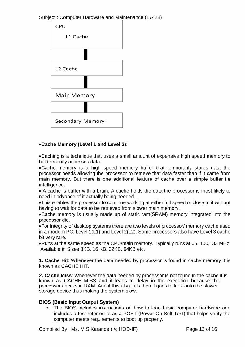
Voltage: 1.5V DDR2: 2008 Module Type: 240-pin DIMM Data Rate: 12800 MBps to 25600 MBps. Cache Memory (Level 1 and Level 2):
Subject : Computer Hardware and Maintenance (17428)
Compiled By : Ms. M.S.Karande (I/c HOD-IF) Page 13 of 16
Cache Memory (Level 1 and Level 2):
Caching is a technique that uses a small amount of expensive high speed memory to hold recently accesses data.
Cache memory is a high speed memory buffer that temporarily stores data the processor needs allowing the processor to retrieve that data faster than if it came from main memory. But there is one additional feature of cache over a simple buffer i.e intelligence.
A cache is buffer with a brain. A cache holds the data the processor is most likely to need in advance of it actually being needed.
This enables the processor to continue working at either full speed or close to it without having to wait for data to be retrieved from slower main memory.
Cache memory is usually made up of static ram(SRAM) memory integrated into the processor die.
For integrity of desktop systems there are two levels of processor/ memory cache used in a modern PC: Level 1(L1) and Level 2(L2). Some processors also have Level 3 cache bit very rare.
Runs at the same speed as the CPU/main memory. Typically runs at 66, 100,133 MHz. Available in Sizes 8KB, 16 KB, 32KB, 64KB etc. 1. Cache Hit: Whenever the data needed by processor is found in cache memory it is known as CACHE HIT.
2. Cache Miss: Whenever the data needed by processor is not found in the cache it is known as CACHE MISS and it leads to delay in the execution because the processor checks in RAM. And if this also fails then it goes to look onto the slower storage device thus making the system slow. BIOS (Basic Input Output System)
• The BIOS includes instructions on how to load basic computer hardware and includes a test referred to as a POST (Power On Self Test) that helps verify the computer meets requirements to boot up properly.
CPU
L1 Cache
L2 Cache
Main Memory
Secondary Memory

Subject : Computer Hardware and Maintenance (17428)
Compiled By : Ms. M.S.Karande (I/c HOD-IF) Page 14 of 16
• If the computer does not pass the POST, you will receive a combination of beeps indicating what is malfunctioning within the computer.
Main functions of BIOS
• The four main functions of a PC BIOS 1. POST - Test the computer hardware and make sure no errors exist before loading
the operating system 2. Bootstrap Loader - Locate the operating system. If a capable operating system
is located, the BIOS will pass control to it. 3. BIOS drivers - Low level drivers that give the computer basic operational control
over your computer's hardware. 4. BIOS/ CMOS Setup - Configuration program that allows you to configure
hardware settings including system settings such as computer passwords, time, and date.
Features of BIOS Standard CMOS Features: It is used to set time date, hard disk type, type of floppy drive, type of monitor and keyboard. Advanced BIOS features The Advanced BIOS Features section enables a user to change numerous settings in their computers BIOS Advanced Chipset Features: It is used to set features of chipset. Power Management Setup: It is used to setup power management settings for the system. PCI/Plug and Play Configurations: It is used to set options of PCI bus and that of plug and play devices. Integrated Peripherals: Allows you to configure, enable or disable on-board ports. PCI Health Status: This submenu allows you to monitor the hardware of your system. CMOS (Complementary Metal Oxide Semiconductor) Set up
During booting by pressing a function key F2 or del key CMOS (Complementary Metal Oxide Semiconductor) Set up utility is used in a PC to set up the basic properties of a computer as given below.
Standard CMOS Setup: It is used to set time date, hard disk type, type of floppy drive, type of monitor and keyboard.
Advanced CMOS Setup: It is used to set typematic rate and delay, above 1 MB memory test, memory test tick sound, Hil < Del> message display, system boot up sequence etc.
Advanced Chipset Setup: It is used to set features of chipset.
Power Management Setup: It is used to control power conservation options.
PCI/Plug and Play Setup: It is used to set options of PCI bus and that of plug and play devices.
Peripherals Setup: It is used to control options related to I/O controllers.
CPU Configuration Setup: This setup is used to select the types of CPU installed in the motherboard. In AMI BIOS, the setting automatically finds out the type of CPU in the computer system. Importance: 1. Used to set date and time, which in turn can be helpful to keep the system up-to-date. 2. Setting up various peripheral automatically or manually. 3. Enable or disable the devices used in the system. 4. Stores information that is updated
Subject : Computer Hardware and Maintenance (17428)
Compiled By : Ms. M.S.Karande (I/c HOD-IF) Page 15 of 16
Motherboard Selection Criteria 1) Motherboard Chipset: Motherboard should use a high performance chipset that
supports DDR or DDR2 SDRAM DIMMs. It should also support PCI- Express X16 video support and Serial ATA or faster hard drive support.
2) Processor: A modern system should use a socket based processor with on-die L2 cache. The processor should have highest speed CPU bus (Front Side Bus: FSB).
3) Processor Sockets: For maximum upgradability and performance, a socket based system should be used.
4) Motherboard Speed: 200MHz to 400MHz for Duron/Athlon/Athlon XP –based boards and 400MHz to 1066MHz for Pentium 4 based boards.
5) Cache Memory: Use a processor with full core speed on-die L2 cache as it offers maximum in performance.
6) SIMM/DIMM/RIMM memory: Current systems use either DDR or DDR2 DIMMs. Currently DDR and DDR2 SDRAM and RDRAM are the fastest type of memory available, with RDRAM being by far the most costly.
7) Bus Type: Current systems offer PCI as well as PCI Express slots. PCI slots should confirm with PCI 2.1 or later revision. Systems without on-board video should also feature PCI Express X 16 slot.
8) Basic Input Output System (BIOS): The motherboard should use industry standard BIOS such as those from AMI, Phoenix or Award. The BIOS should be of a flash ROM or EEPROM design for easy updating.
9) Form Factor: For maximum flexibility, performance, reliability and ease of use, motherboard with ATX form factor should be used.
10) Built-in Interfaces: The motherboard should contain as many built-in standard controllers and interfaces as possible.
11) On-board IDE interfaces: It should be included on the motherboard. 12) Power Management: The motherboard should support the latest standard for
power management which is ACPI. 13) Documentation: Good technical documentation is essential. It should
include information on all jumpers and switches found on the board, connector pin out for all connectors, specifications for other plug-in components etc.
14) Technical Support: Good online technical support goes beyond documentation. It includes driver and BIOS updates, FAQs, updated tables of processor and memory compatibility, and the utility programs to help you monitor the condition of your system.
Questions
1. Write any four features of PCI bus 2. State any four features of P67 chipset 3. What is cache hit and cache miss? Describe L1, L2 and L3 cache.(8M) 4. Define the terms cache hit and cache miss.(2M) )(S-14) (W-14) 5. State any eight motherboard selection criterion.(8 M) 6. State any three functions of BIOS. 7. Describe the use of address bus, data bus, and control bus 8. What is cache memory? What is L1, L2, L3 cache? (8M) 9. Draw the block diagram of North bridge / South bridge architecture and describe
the various blocks (8M) 10. Compare DDR2 and DDR3 (Any four points) 11. What is hyper threading technology? What is its requirement?

Subject : Computer Hardware and Maintenance (17428)
Compiled By : Ms. M.S.Karande (I/c HOD-IF) Page 16 of 16
12. Compare DDR2 and DDR3 with respect to clock frequency, transfer rate, bank used and voltage required. (4 M)(S-14)
13. Compare PCI with PCI-express bus.(4M) (S-14) 14. What are the different modes of operation of CPU? (8M)(S-14) 15. Draw the block diagram of Northbridge/ Southbridge architecture and
describe various blocks.(8M)(S-14) 16. Write any four features of PCI bus 17. State any four features of P67 chipset 18. What is cache hit and cache miss? Describe L1, L2 and L3 cache.(8M) 19. Define the terms cache hit and cache miss.(2M) )(S-14) (W-14) 20. State any eight motherboard selection criterion.(8 M) 21. State any three functions of BIOS. 22. Describe the use of address bus, data bus, and control bus 23. What is cache memory? What is L1, L2, L3 cache? (8M) 24. Draw the block diagram of North bridge / South bridge architecture and describe
the various blocks (8M) 25. Compare DDR2 and DDR3 (Any four points) 26. What is hyper threading technology? What is its requirement? 27. Compare DDR2 and DDR3 with respect to clock frequency, transfer rate,
bank used and voltage required. (4 M)(S-14) 28. Compare PCI with PCI-express bus.(4M) (S-14) 29. What are the different modes of operation of CPU? (8M)(S-14) 30. Draw the block diagram of Northbridge/ Southbridge architecture and
describe various blocks.(8M)(S-14) 31. Write two important features of the following:
i. SDRAM ii. DDR iii. Cache iv. DDR2 ( 8M S-15)
32. Draw and explain the north and south bridge chipset architecture. (Diagram 4 Marks, Explanation 4 Marks) (8M S-15)