Embed Size (px)
Citation preview

1
IPZA60R060P7
Rev.2.0,2017-11-24Final Data Sheet
123 4
PG-TO247-4-3
DrainPin 1
GatePin 4
PowerSourcePin 2
DriverSourcePin 3
MOSFET600VCoolMOS™P7PowerTransistorTheCoolMOS™7thgenerationplatformisarevolutionarytechnologyforhighvoltagepowerMOSFETs,designedaccordingtothesuperjunction(SJ)principleandpioneeredbyInfineonTechnologies.The600VCoolMOS™P7seriesisthesuccessortotheCoolMOS™P6series.ItcombinesthebenefitsofafastswitchingSJMOSFETwithexcellenteaseofuse,e.g.verylowringingtendency,outstandingrobustnessofbodydiodeagainsthardcommutationandexcellentESDcapability.Furthermore,extremelylowswitchingandconductionlossesmakeswitchingapplicationsevenmoreefficient,morecompactandmuchcooler.
Features•Suitableforhardandsoftswitching(PFCandLLC)duetoanoutstanding commutationruggedness•Significantreductionofswitchingandconductionlosses•ExcellentESDrobustness>2kV(HBM)forallproducts•BetterRDS(on)/packageproductscomparedtocompetitionenabledbya lowRDS(on)*A(below1Ohm*mm²)
Benefits•Easeofuseandfastdesign-inthroughlowringingtendencyandusage acrossPFCandPWMstages•Simplifiedthermalmanagementduetolowswitchingandconduction losses•Increasedpowerdensitysolutionsenabledbyusingproductswith smallerfootprintandhighermanufacturingqualitydueto>2kVESD protection•Suitableforawidevarietyofapplicationsandpowerranges
PotentialapplicationsPFCstages,hardswitchingPWMstagesandresonantswitchingstagesfore.g.PCSilverbox,Adapter,LCD&PDPTV,Lighting,Server,TelecomandUPS.
ProductValidation:QualifiedforindustrialapplicationsaccordingtotherelevanttestsofJEDEC47/20/22
Pleasenote:ForMOSFETparallelingtheuseofferritebeadsonthegateorseparatetotempolesisgenerallyrecommended.
Table1KeyPerformanceParametersParameter Value UnitVDS @ Tj,max 650 V
RDS(on),max 60 mΩ
Qg,typ 67 nC
ID,pulse 151 A
Eoss @ 400V 7.1 µJ
Body diode diF/dt 900 A/µs
Type/OrderingCode Package Marking RelatedLinksIPZA60R060P7 PG-TO 247-4-3 60R060P7 see Appendix A

2
600VCoolMOS™P7PowerTransistorIPZA60R060P7
Rev.2.0,2017-11-24Final Data Sheet
TableofContentsDescription . . . . . . . . . . . . . . . . . . . . . . . . . . . . . . . . . . . . . . . . . . . . . . . . . . . . . . . . . . . . . . . . . . . . . . . . . . . . . 1
Maximum ratings . . . . . . . . . . . . . . . . . . . . . . . . . . . . . . . . . . . . . . . . . . . . . . . . . . . . . . . . . . . . . . . . . . . . . . . . 3
Thermal characteristics . . . . . . . . . . . . . . . . . . . . . . . . . . . . . . . . . . . . . . . . . . . . . . . . . . . . . . . . . . . . . . . . . . . . 4
Electrical characteristics . . . . . . . . . . . . . . . . . . . . . . . . . . . . . . . . . . . . . . . . . . . . . . . . . . . . . . . . . . . . . . . . . . . 5
Electrical characteristics diagrams . . . . . . . . . . . . . . . . . . . . . . . . . . . . . . . . . . . . . . . . . . . . . . . . . . . . . . . . . . . 7
Test Circuits . . . . . . . . . . . . . . . . . . . . . . . . . . . . . . . . . . . . . . . . . . . . . . . . . . . . . . . . . . . . . . . . . . . . . . . . . . . 11
Package Outlines . . . . . . . . . . . . . . . . . . . . . . . . . . . . . . . . . . . . . . . . . . . . . . . . . . . . . . . . . . . . . . . . . . . . . . . 12
Appendix A . . . . . . . . . . . . . . . . . . . . . . . . . . . . . . . . . . . . . . . . . . . . . . . . . . . . . . . . . . . . . . . . . . . . . . . . . . . . 13
Revision History . . . . . . . . . . . . . . . . . . . . . . . . . . . . . . . . . . . . . . . . . . . . . . . . . . . . . . . . . . . . . . . . . . . . . . . . 14
Trademarks . . . . . . . . . . . . . . . . . . . . . . . . . . . . . . . . . . . . . . . . . . . . . . . . . . . . . . . . . . . . . . . . . . . . . . . . . . . 14
Disclaimer . . . . . . . . . . . . . . . . . . . . . . . . . . . . . . . . . . . . . . . . . . . . . . . . . . . . . . . . . . . . . . . . . . . . . . . . . . . . 14

3
600VCoolMOS™P7PowerTransistorIPZA60R060P7
Rev.2.0,2017-11-24Final Data Sheet
1MaximumratingsatTj=25°C,unlessotherwisespecified
Table2MaximumratingsValues
Min. Typ. Max.Parameter Symbol Unit Note/TestCondition
Continuous drain current1) ID --
--
4830 A TC=25°C
TC=100°C
Pulsed drain current2) ID,pulse - - 151 A TC=25°C
Avalanche energy, single pulse EAS - - 159 mJ ID=6.4A; VDD=50V; see table 10
Avalanche energy, repetitive EAR - - 0.80 mJ ID=6.4A; VDD=50V; see table 10
Avalanche current, single pulse IAS - - 6.4 A -
MOSFET dv/dt ruggedness dv/dt - - 80 V/ns VDS=0...400VGate source voltage (static) VGS -20 - 20 V static;
Gate source voltage (dynamic) VGS -30 - 30 V AC (f>1 Hz)
Power dissipation Ptot - - 164 W TC=25°CStorage temperature Tstg -55 - 150 °C -
Operating junction temperature Tj -55 - 150 °C -
Mounting torque - - - 60 Ncm M3 and M3.5 screws
Continuous diode forward current IS - - 48 A TC=25°CDiode pulse current2) IS,pulse - - 151 A TC=25°C
Reverse diode dv/dt3) dv/dt - - 50 V/ns VDS=0...400V,ISD<=48A,Tj=25°C see table 8
Maximum diode commutation speed diF/dt - - 900 A/µs VDS=0...400V,ISD<=48A,Tj=25°C see table 8
Insulation withstand voltage VISO - - n.a. V Vrms,TC=25°C,t=1min
1) Limited by Tj,max. Maximum Duty Cycle D = 0.502) Pulse width tp limited by Tj,max3) Identical low side and high side switch with identical RG

4
600VCoolMOS™P7PowerTransistorIPZA60R060P7
Rev.2.0,2017-11-24Final Data Sheet
2Thermalcharacteristics
Table3ThermalcharacteristicsValues
Min. Typ. Max.Parameter Symbol Unit Note/TestCondition
Thermal resistance, junction - case RthJC - - 0.76 °C/W -
Thermal resistance, junction - ambient RthJA - - 62 °C/W leaded
Thermal resistance, junction - ambientfor SMD version RthJA - - - °C/W -
Soldering temperature, wavesolderingonly allowed at leads Tsold - - 260 °C 1.6mm (0.063 in.) from case for 10s
5
600VCoolMOS™P7PowerTransistorIPZA60R060P7
Rev.2.0,2017-11-24Final Data Sheet
3ElectricalcharacteristicsatTj=25°C,unlessotherwisespecified
Table4StaticcharacteristicsValues
Min. Typ. Max.Parameter Symbol Unit Note/TestCondition
Drain-source breakdown voltage V(BR)DSS 600 - - V VGS=0V,ID=1mAGate threshold voltage V(GS)th 3 3.5 4 V VDS=VGS,ID=0.8mA
Zero gate voltage drain current IDSS --
-10
1- µA VDS=600V,VGS=0V,Tj=25°C
VDS=600V,VGS=0V,Tj=150°C
Gate-source leakage current IGSS - - 100 nA VGS=20V,VDS=0V
Drain-source on-state resistance RDS(on)--
0.0490.115
0.060- Ω VGS=10V,ID=15.9A,Tj=25°C
VGS=10V,ID=15.9A,Tj=150°C
Gate resistance RG - 2.8 - Ω f=1MHz,opendrain
Table5DynamiccharacteristicsValues
Min. Typ. Max.Parameter Symbol Unit Note/TestCondition
Input capacitance Ciss - 2895 - pF VGS=0V,VDS=400V,f=250kHzOutput capacitance Coss - 48 - pF VGS=0V,VDS=400V,f=250kHz
Effective output capacitance, energyrelated1) Co(er) - 89 - pF VGS=0V,VDS=0...400V
Effective output capacitance, timerelated2) Co(tr) - 925 - pF ID=constant,VGS=0V,VDS=0...400V
Turn-on delay time td(on) - 23 - ns VDD=400V,VGS=13V,ID=15.9A,RG=3.3Ω;seetable9
Rise time tr - 8 - ns VDD=400V,VGS=13V,ID=15.9A,RG=3.3Ω;seetable9
Turn-off delay time td(off) - 79 - ns VDD=400V,VGS=13V,ID=15.9A,RG=3.3Ω;seetable9
Fall time tf - 4 - ns VDD=400V,VGS=13V,ID=15.9A,RG=3.3Ω;seetable9
Table6GatechargecharacteristicsValues
Min. Typ. Max.Parameter Symbol Unit Note/TestCondition
Gate to source charge Qgs - 15 - nC VDD=400V,ID=15.9A,VGS=0to10VGate to drain charge Qgd - 20 - nC VDD=400V,ID=15.9A,VGS=0to10VGate charge total Qg - 67 - nC VDD=400V,ID=15.9A,VGS=0to10VGate plateau voltage Vplateau - 5.2 - V VDD=400V,ID=15.9A,VGS=0to10V
1)Co(er)isafixedcapacitancethatgivesthesamestoredenergyasCosswhileVDSisrisingfrom0to400V2)Co(tr)isafixedcapacitancethatgivesthesamechargingtimeasCosswhileVDSisrisingfrom0to400V

6
600VCoolMOS™P7PowerTransistorIPZA60R060P7
Rev.2.0,2017-11-24Final Data Sheet
Table7ReversediodecharacteristicsValues
Min. Typ. Max.Parameter Symbol Unit Note/TestCondition
Diode forward voltage VSD - 0.9 - V VGS=0V,IF=15.9A,Tj=25°C
Reverse recovery time trr - 254 - ns VR=400V,IF=6A,diF/dt=100A/µs;see table 8
Reverse recovery charge Qrr - 2.9 - µC VR=400V,IF=6A,diF/dt=100A/µs;see table 8
Peak reverse recovery current Irrm - 23.1 - A VR=400V,IF=6A,diF/dt=100A/µs;see table 8
7
600VCoolMOS™P7PowerTransistorIPZA60R060P7
Rev.2.0,2017-11-24Final Data Sheet
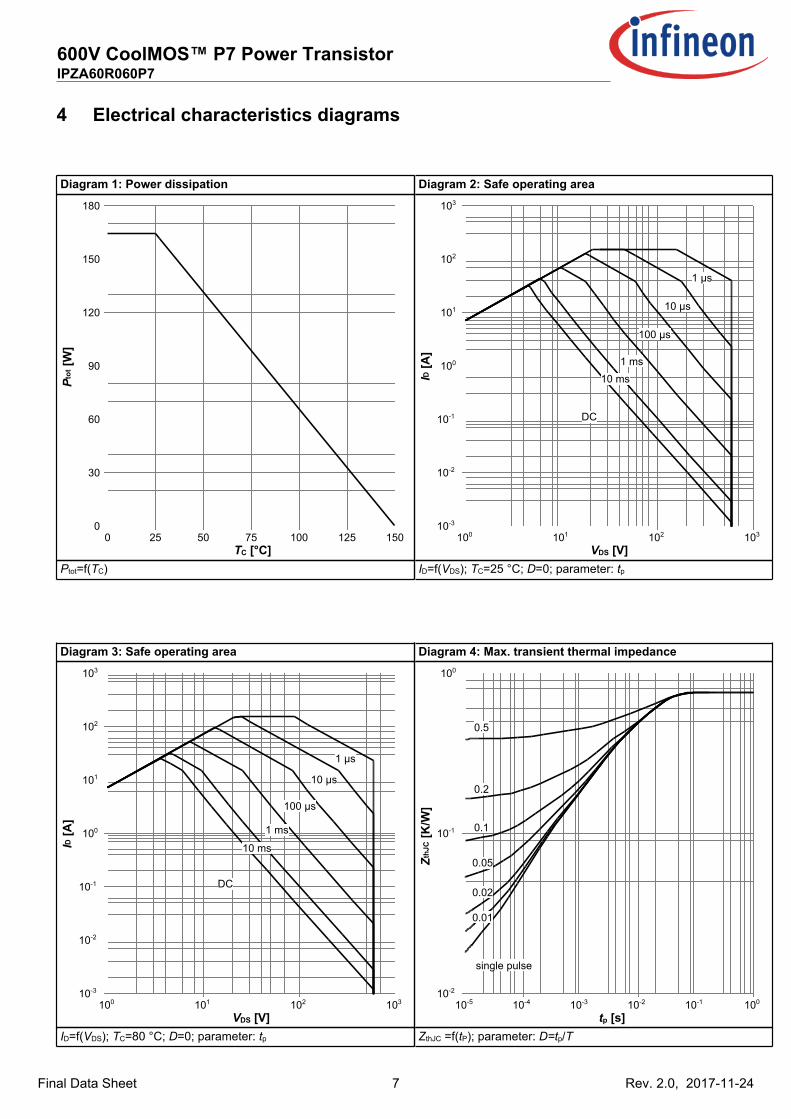
4Electricalcharacteristicsdiagrams
Diagram1:Powerdissipation
TC[°C]
Ptot[W
]
0 25 50 75 100 125 1500
30
60
90
120
150
180
Ptot=f(TC)
Diagram2:Safeoperatingarea
VDS[V]
ID[A
]
100 101 102 10310-3
10-2
10-1
100
101
102
103
1 µs
10 µs
100 µs
1 ms
10 ms
DC
ID=f(VDS);TC=25°C;D=0;parameter:tp
Diagram3:Safeoperatingarea
VDS[V]
ID[A
]
100 101 102 10310-3
10-2
10-1
100
101
102
103
1 µs
10 µs
100 µs
1 ms
10 ms
DC
ID=f(VDS);TC=80°C;D=0;parameter:tp
Diagram4:Max.transientthermalimpedance
tp[s]
ZthJC[K
/W]
10-5 10-4 10-3 10-2 10-1 10010-2
10-1
100
0.5
0.2
0.05
0.1
0.02
0.01
single pulse
ZthJC=f(tP);parameter:D=tp/T

8
600VCoolMOS™P7PowerTransistorIPZA60R060P7
Rev.2.0,2017-11-24Final Data Sheet
Diagram5:Typ.outputcharacteristics
VDS[V]
ID[A
]
0 5 10 15 200
50
100
150
200
20 V
10 V
8 V
7 V
6 V
5.5 V
5 V
4.5 V
ID=f(VDS);Tj=25°C;parameter:VGS
Diagram6:Typ.outputcharacteristics
VDS[V]
ID[A
]
0 5 10 15 200
20
40
60
80
100
12020 V
10 V
8 V
7 V
6 V
5.5 V
5 V
4.5 V
ID=f(VDS);Tj=125°C;parameter:VGS
Diagram7:Typ.drain-sourceon-stateresistance
ID[A]
RDS(on
) [Ω]
0 20 40 60 80 100 1200.100
0.130
0.160
0.190
0.220
0.250
20 V
7 V
10 V
6.5 V
6 V5.5 V
RDS(on)=f(ID);Tj=125°C;parameter:VGS
Diagram8:Drain-sourceon-stateresistance
Tj[°C]
RDS(on
) [no
rmalized]
-50 -25 0 25 50 75 100 125 1500.000
0.500
1.000
1.500
2.000
2.500
3.000
RDS(on)=f(Tj);ID=15.9A;VGS=10V

9
600VCoolMOS™P7PowerTransistorIPZA60R060P7
Rev.2.0,2017-11-24Final Data Sheet
Diagram9:Typ.transfercharacteristics
VGS[V]
ID[A
]
0 2 4 6 8 10 120
50
100
150
200
150 °C
25 °C
ID=f(VGS);VDS=20V;parameter:Tj
Diagram10:Typ.gatecharge
Qgate[nC]
VGS [V]
0 10 20 30 40 50 60 70 800
2
4
6
8
10
12
120 V 400 V
VGS=f(Qgate);ID=15.9Apulsed;parameter:VDD
Diagram11:Forwardcharacteristicsofreversediode
VSD[V]
IF [A]
0.0 0.2 0.4 0.6 0.8 1.0 1.2 1.4 1.6 1.810-1
100
101
102
103
125 °C 25 °C
IF=f(VSD);parameter:Tj
Diagram12:Avalancheenergy
Tj[°C]
EAS [mJ]
25 50 75 100 125 1500
50
100
150
200
EAS=f(Tj);ID=6.4A;VDD=50V

10
600VCoolMOS™P7PowerTransistorIPZA60R060P7
Rev.2.0,2017-11-24Final Data Sheet
Diagram13:Drain-sourcebreakdownvoltage
Tj[°C]
VBR(DSS
) [V]
-50 -25 0 25 50 75 100 125 150540
550
560
570
580
590
600
610
620
630
640
650
660
670
680
690
VBR(DSS)=f(Tj);ID=1mA
Diagram14:Typ.capacitances
VDS[V]
C[p
F]
0 100 200 300 400 500100
101
102
103
104
105
Ciss
Coss
Crss
C=f(VDS);VGS=0V;f=250kHz
Diagram15:Typ.Cossstoredenergy
VDS[V]
Eoss[µ
J]
0 100 200 300 400 5000
2
4
6
8
10
Eoss=f(VDS)

11
600VCoolMOS™P7PowerTransistorIPZA60R060P7
Rev.2.0,2017-11-24Final Data Sheet
5TestCircuits
Table8DiodecharacteristicsTest circuit for diode characteristics Diode recovery waveform
VDS
IF
Rg1
Rg 2
Rg1 = Rg 2
Table9Switchingtimes(ss)Switching times test circuit for inductive load Switching times waveform
VDS
VGS
td(on) td(off)tr
ton
tf
toff
10%
90%
VDS
VGS
Table10Unclampedinductiveload(ss)Unclamped inductive load test circuit Unclamped inductive waveform
VDS
V(BR)DS
IDVDS
VDSID

12
600VCoolMOS™P7PowerTransistorIPZA60R060P7
Rev.2.0,2017-11-24Final Data Sheet
6PackageOutlines
DIMENSIONSMIN. MAX.
A2
L
b
D
c
b2
E
e1
L1
Q
øP2
D1
A
A1
2.101.90
5.08
19.80
-
20.90
0.58
0.65
15.70
5.60
2.40
16.25
20.10
0.79
0.66
0.20
21.10
6.00
2.60
4.30
15.90
16.85
MILLIMETERS
4.90
2.31
5.10
2.51
b1
1.10 1.30
b3
PG-TO247-4-3
SCALE
Z8B00184785
REVISION
ISSUE DATE
EUROPEAN PROJECTION
03
21.08.2017
0 5
DOCUMENT NO.
2:1
A3 0.250.05
D2 1.05 1.35
D3 24.97 25.27
10mm
E1 13.10 13.50
E2 2.40 2.60
-
øP1 7.00 7.40
øP 3.50 3.70
S 6.15
T 9.80 10.20
U 6.00 6.40
1.34 1.44
e2 2.79
e3 2.54
D4 4.90 5.10
Figure 1 Outline PG-TO 247-4-3, dimensions in mm - Industrial Grade

13
600V CoolMOS™ P7 Power TransistorIPZA60R060P7
Rev. 2.0, 2017-11-24Final Data Sheet
7 Appendix A
Table 11 Related Links
• IFX CoolMOS P7 Webpage: www.infineon.com
• IFX CoolMOS P7 application note: www.infineon.com
• IFX CoolMOS P7 simulation model: www.infineon.com
• IFX Design tools: www.infineon.com

14
600V CoolMOS™ P7 Power TransistorIPZA60R060P7
Rev. 2.0, 2017-11-24Final Data Sheet
Revision History
IPZA60R060P7
Revision: 2017-11-24, Rev. 2.0
Previous Revision
Revision Date Subjects (major changes since last revision)
2.0 2017-11-24 Release of final version
Trademarks of Infineon Technologies AG
AURIX™, C166™, CanPAK™, CIPOS™, CoolGaN™, CoolMOS™, CoolSET™, CoolSiC™, CORECONTROL™, CROSSAVE™, DAVE™, DI-POL™, DrBlade™,EasyPIM™, EconoBRIDGE™, EconoDUAL™, EconoPACK™, EconoPIM™, EiceDRIVER™, eupec™, FCOS™, HITFET™, HybridPACK™, Infineon™,ISOFACE™, IsoPACK™, i-Wafer™, MIPAQ™, ModSTACK™, my-d™, NovalithIC™, OmniTune™, OPTIGA™, OptiMOS™, ORIGA™, POWERCODE™,PRIMARION™, PrimePACK™, PrimeSTACK™, PROFET™, PRO-SIL™, RASIC™, REAL3™, ReverSave™, SatRIC™, SIEGET™, SIPMOS™, SmartLEWIS™,SOLID FLASH™, SPOC™, TEMPFET™, thinQ!™, TRENCHSTOP™, TriCore™.
Trademarks updated August 2015
Other Trademarks
All referenced product or service names and trademarks are the property of their respective owners.
We Listen to Your CommentsAny information within this document that you feel is wrong, unclear or missing at all? Your feedback will help us to continuouslyimprove the quality of this document. Please send your proposal (including a reference to this document) to:[email protected]
Published byInfineon Technologies AG81726 München, Germany© 2017 Infineon Technologies AGAll Rights Reserved.
Legal DisclaimerThe information given in this document shall in no event be regarded as a guarantee of conditions or characteristics (“Beschaffenheitsgarantie”) .
With respect to any examples, hints or any typical values stated herein and/or any information regarding the application of theproduct, Infineon Technologies hereby disclaims any and all warranties and liabilities of any kind, including without limitationwarranties of non-infringement of intellectual property rights of any third party.In addition, any information given in this document is subject to customer’s compliance with its obligations stated in thisdocument and any applicable legal requirements, norms and standards concerning customer’s products and any use of theproduct of Infineon Technologies in customer’s applications.The data contained in this document is exclusively intended for technically trained staff. It is the responsibility of customer’stechnical departments to evaluate the suitability of the product for the intended application and the completeness of the productinformation given in this document with respect to such application.
InformationFor further information on technology, delivery terms and conditions and prices please contact your nearest InfineonTechnologies Office (www.infineon.com ).
WarningsDue to technical requirements, components may contain dangerous substances. For information on the types in question,please contact the nearest Infineon Technologies Office.The Infineon Technologies component described in this Data Sheet may be used in life-support devices or systems and/orautomotive, aviation and aerospace applications or systems only with the express written approval of Infineon Technologies, if afailure of such components can reasonably be expected to cause the failure of that life-support, automotive, aviation andaerospace device or system or to affect the safety or effectiveness of that device or system. Life support devices or systems areintended to be implanted in the human body or to support and/or maintain and sustain and/or protect human life. If they fail, it isreasonable to assume that the health of the user or other persons may be endangered.