Embed Size (px)
Citation preview
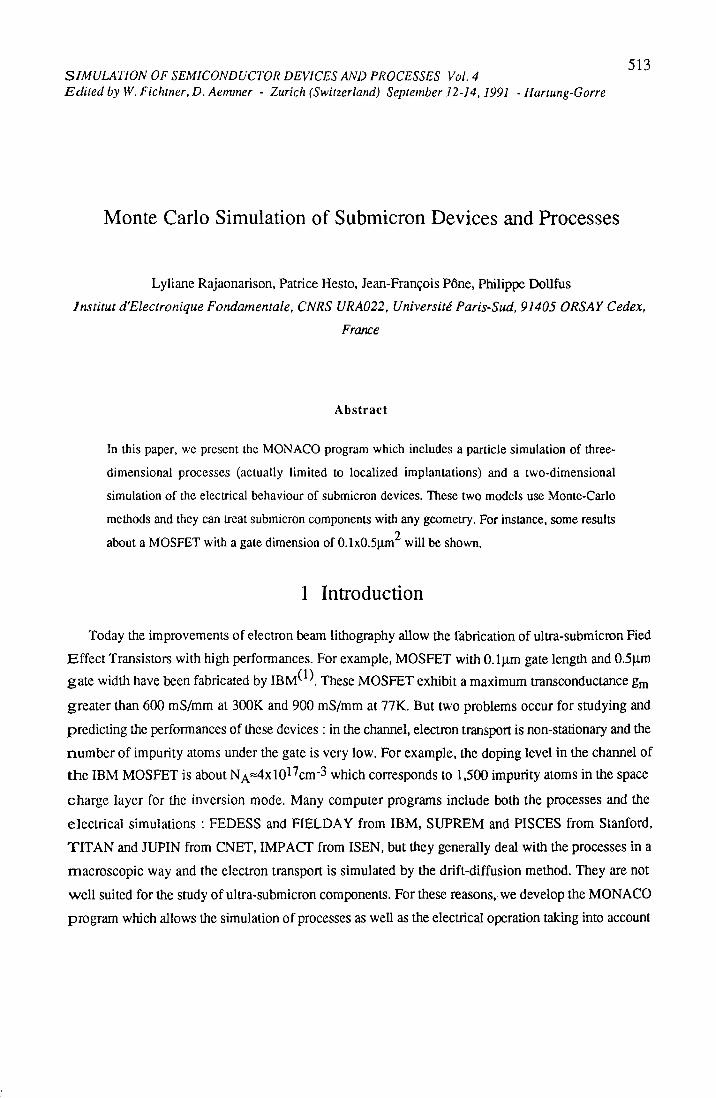
SIMULATION OF SEMICONDUCTOR DEVICES AND PROCESSES Vol. 4 Edited by W, FicInner, D.Aemmer - Zurich (Switzerland) September 12-14,1991 - Hartung-Gorre
Monte Carlo Simulation of Submicron Devices and Processes
Lyliane Rajaonarison, Patrice Hesto, Jean-Francois P6ne, Philippe Dollfus
Institut d'Electronique Fondamentale, CNRS URA022, University Paris-Sud, 91405 ORSAY Cedex,
France
Abstract
In this paper, we present the MONACO program which includes a particle simulation of three-
dimensional processes (actually limited to localized implantations) and a two-dimensional
simulation of the electrical behaviour of submicron devices. These two models use Monte-Carlo
methods and they can treat submicron components with any geometry. For instance, some results 2
about a MOSFET with a gate dimension of 0.1x0.5|i.m will be shown.
1 Introduction
Today the improvements of electron beam lithography allow the fabrication of ultra-submicron Fied
Effect Transistors with high performances. For example, MOSFET with 0.1 u.m gate length and 0.5u.m
gate width have been fabricated by IBM* '. These MOSFET exhibit a maximum transconductance gm
greater than 600 mS/mm at 300K and 900 mS/mm at 77K. But two problems occur for studying and
predicting the performances of these devices : in the channel, electron transport is non-stationary and the
number of impurity atoms under the gate is very low. For example, the doping level in the channel of
the IBM MOSFET is about N^=4xl017cm-3 which corresponds to 1,500 impurity atoms in the space
charge layer for the inversion mode. Many computer programs include both the processes and the
electrical simulations : FEDESS and FIELDAY from IBM, SUPREM and PISCES from Stanford,
TITAN and JUPIN from CNET, IMPACT from ISEN, but they generally deal with the processes in a
macroscopic way and the electron transport is simulated by the drift-diffusion method. They are not
well suited for the study of ultra-submicron components. For these reasons, we develop the MONACO
program which allows the simulation of processes as well as the electrical operation taking into account
514
the geometry issued from the processes. Today, the processes which can be treated by MONACO are
limited to localized implantations.
2 Simulation of the localized implantation
2.1 The model
The algorithm is induced from the Monte-Carlo method. It consists of following the trajectory of
every ion until it comes to rest. Every incident ion moves in straight free-flight-paths, separated by
binary collisions with the target atoms. The ion direction is assumed to change as a result of these
collisions. Its energy is transfercd part to the electronic cloud around its trajectory and part to the
"knock-on" atoms. The interaction between incident ion and target ion is treated by a classical
mechanical approach with a randomly selected impact parameter. The interaction potential is the
Moliere's potential at low energies and the Coulomb's potential at high energies. For the electronic
energy losses, we take a calculation according to the LSS (Lindhard-Scharff-Schiott) theory at low
energies and the Bethe and Bloch's equations at high energies^ '.
Actually, our program does not take into account the channeling phenomena which result from ion
scattering into the crystallographic directions of the material. On the other hand, it can deal with all
geometries and all chemical compounds. It has been extended in order to include multilayer structures.
The transition (laterally or in depth) between two materials is immediately delected because the frce-
flight-paths are kept equal to the mean atomic spacing in the target. The nuclear and electronic stopping
powers are assumed to be independent and are changed according to the chemical composition of the
material. The "knock-on" atom is randomly chosen with respect to the material stoichiometry. Then, our
program can simulate the ion implantation in a whole process of any electronic device realization.
2-2 Results for the 0.1|im MOSFET
We have simulated the implantation steps of the fabrication of a 0. Ix0.5|im MOSFET with the true
number of implanted impurity atoms and the various masks used in a self-aligned technology. A
schematic cross section of the device is drawn in Fig. 1.
o The ion implantations are made on a 0.5x0.5um area with an incidence angle normal to the target.
The main processing steps are summarized below :
a)-For the channel:

515
Boron is implanted into the substrate with 6,400 ions at 15keV (=3.2x10 cm ) and 15,400 ions at 12 1 30keV (=7.7x10 cm ). The distribution of boron ions is shown in Fig.2a. We can notice fluctuations
for this distribution with few impurities under the gate oxide, as well as the overdoping in depth
introduced in order to limit the punch-through phenomena resulting from the short channel effects.
b)-For the source and drain extensions :
Antimony implantations into the source and drain extensions is realized through the 4.5nm thick gate
oxide on which is deposited the lOOxlOOnm polysilicon gate, and are grown the overall 7.5nm thick
Si02 layer: 25,000 ions at lOkeV (=1.25xl013cm"2) and 79,500 ions at 20keV (=4xl013cm"2). These
extensions are necessary to delimit the channel length. Indeed, in order to ensure a shallow junction
near the channel and small lateral stragglings under the gate, low energy implantations are useful.
Figure 2b shows the antimony distribution. We can see a small overflow of the S-D extension zones
which reduces the effective gate length. Several donor impurities are stopped by the polysilicon, but
some ions reach the channel via the S-D zones and could disturb the electrical device operation.
c)-For the source and drain contact areas :
Arsenic is implanted into the source and drain contact zones using a sidewall lOOnm thick Si3N4
gate spacer with 770,000 ions at 20keV (=3.9x10 cm )• The relative high dose allows to obtain low
access S-D resistances, but lateral diffusion is made larger (see fig.2-c). Hence, in order to offset the
N4" implant, a sidewall spacer is introduced. A large part of ions are stopped into Si3N4. Some donor
impurities meet the channel side via the S-D regions, but they are in the extension zones, and have there
n o influence on the electrical behaviour of the device.
3 Simulation of the electrical behaviour
3.1 The model
The electrical simulation includes both the description of the electron motion using a particle
Monte-Carlo model taking into account the electric field, and the resolution of Poisson's equation,
considering the applied bias voltages and the distribution of the electric charges. This simulator has been
described previously' '. It can describe the dynamic of electrons and holes in a device with any shape,
15 electrodes and 30 various materials at most. Carrier-phonon scattering involve both acoustic and
optical phonons, with coupling by deformation potential and by Coulomb interaction for polar
materials. For simple cases, a 2DK approach exists. For the conduction band, we have a three valley
model r L X (if they exist) and for the valence band, a two valley model (heavy and light holes). We
take into account the energy band non-parabolicity. The ohmic contact zones are modelled by

516
Generation-Recombination centers with infinite velocity. The effect of an ionizing particle (generation of
electron-hole pairs along the track) can also be treated. We use a classical approach for the
heterojunction crossing. For the resolution of the Poisson's equation, the carrier densities arc means
over space and over time. The time step is inferior to the smallest dielectric relaxation time (in the
highest doped zone) and the mesh size is rectangular (cell lengths are about the Debye's length).
3-2 Results for the (U^m MOSFET
Concerning the electrical behaviour of the 0.1x0.5|xm MOSFET, we have only simulated the dotted
rectangular plotted in Fig.l. We have taken a large part of drain extension in order that electrons can
thermalize themself before reaching the drain contact. The number of impurity atoms per mesh used to
calculate the potential is derived from the implantation simulations. We notice, considering the small
dimensions of the device, that it works with the true number of impurity atoms and carriers (30,000 in
this case). On the other hand, we take thin meshing (mesh dimensions, in the channel, under the gate,
are 2x2.5nm2); this means that the distribution of acceptor atoms is very noisy because inside each
mesh there are 0, 1 or 2 atoms (see Fig.3). The same phenomena occur in the source and drain regions.
Nevertheless, our computer program is still stable.
Figure 6 displays the IDS~^DS characteristics for fixed VQ§ with error bars on current amplitude.
There is a good saturation of Irjs- This figure also shows the variations of the saturation current lossat
versus VQJ. It is worth noting that this current increases linearly with the gate voltage, this means that
the saturation phenomena do not come from the channel pinch off (in this case IoSsat would be
proportional to the square of VQS-VT). Furthermore the transconductance gm is about 800 mS/mm.
We have investigated the electron behaviour in the channel. At every time, we know the position, the
kinetic energy and the velocity components of each electron. Figure 5 shows the distribution of the
mean velocity in the source-drain direction for the electrons, in a 20nm thick channel parallel to the
oxide interface under the gate. We note that this velocity increases throughout the channel and reaches
3.5xl0^cm.s"* at the drain side, against the interface. As the saturation velocity of electrons in silicon is
less than lO^cm.s"1, we can conclude that electron transport is non-stationary . This means that
electrons suffer only few scattering during their motion in the channel. In silicon, two main types of
interaction occur with about the same frequencies: clastic scattering (acoustic, impurity) and inelastic
scattering with emission of a 50 meV phonon (non-polar optic and equivalent intervalley interactions).
In these conditions, the variations of the total energy (kinetic energy + potential energy) of the electrons
give the number of inelastic interactions suffered by electrons during their transit across the channel.
The total carrier energy is plotted in Fig.6. The dotted line represents the maximum energy of electrons
in the channel, if they were purely ballistic. In fact, they loose an energy of about 0.3eV which

517
corresponds to the emission of about 6 phonons. This value falls in good agreement with the frequency
of inelastic interactions (=1013 Hz) which yields one interaction every O.lps , that is about 7 phonon
emissions during the transit time (=0.7ps).
4 Conclusion
We have developed a particle ensemble Monte-Carlo model allowing the simulation of both the
processes (actually limited to localized implantations) and the electrical behaviour of submicron devices.
The programs take into account the problems coming from the decrease of the component dimensions
(the spatial distribution of impurity atoms and the non-stationary transport phenomena).
References
(1) KERN.D.P., 19th European Solid State Device Research Conference, Berlin, 1989, (Eds.,
Heuberger.A., Rysscl.H., Lange.P., Springer-Verlag), p.633
(2) BIERSACK.J.P., HAGGMARK.L.G., Nucl. Instr. and Meth., 174, (1980), p257
(3) HESTO.P., PONE.J-F, MOUIS.M., PELOUARD.J-L., CASTAGNE.R., Nasecode IV
Conference, Dublin, 1985, (Ed., Miller.J.J.H., Boole Press), p315

518
f VG
Vs Si02 7.5nm
Source extensic
Drain Gate extensii n oxide
substrate (Sli) 4 5 n m
VSub
Figure 1: Cross section of the lOOnm gate length MOSFET.
V D
Boron
f f f W W w
Arsenic
Antimony
HIHI W W W 1 1 1
Si02 7.5 nrri
Si3N4
/ Si02 4.5nm T
lOOnm L lOOnm
Si poly
^Wff
Substrate (Si)
(C)
Figure 2: Distribution of the acceptor impurities (Boron: a), and of the donor impurities (Antimony: b
and Arsenic: c)
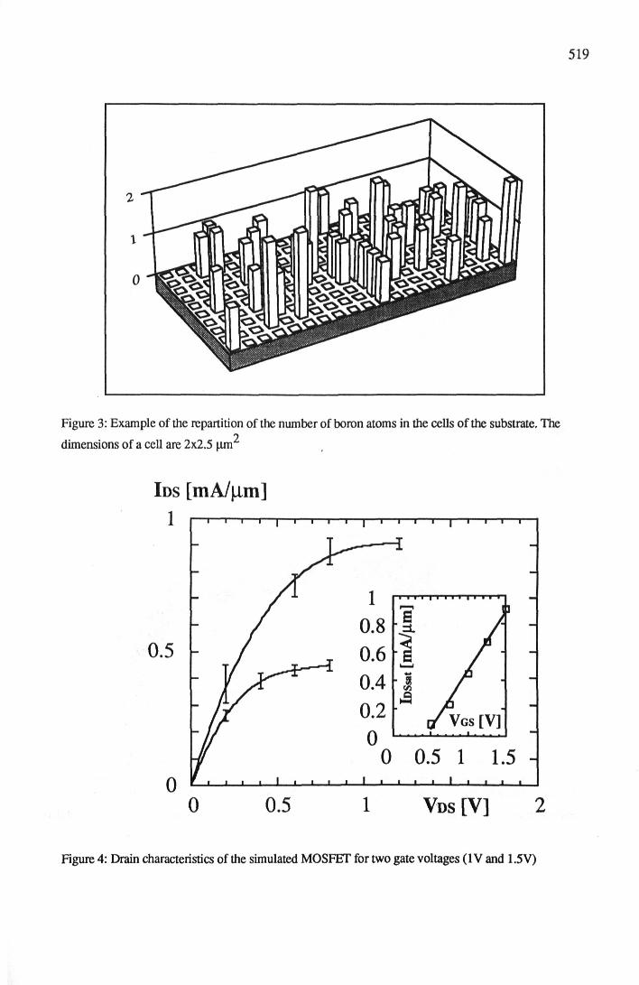
Figure 3: Example of the repartition of the number of boron atoms in the cells of the substrate. The
dimensions of a cell are 2x2.5 um
IDS [mA/jim] T — i — i — i — | — i — r — i — i — | — i — i — i — i — | — i — r - — i — r
0 0.5 1 VDS[V] 2
Figure 4: Drain characteristics of the simulated MOSFET for two gate voltages (IV and 1.5V)

520
Figure 5: Mean velocity in the source drain direction for the electrons under the gate oxide. The 7
velocities are in 10 cm/s and the dimentions are in nm. The source is at the left, the drain is at the right
and the gate oxide is at the back.
Figure 5: The total energy Qcinetic + potential) for the electrons under the gate. The energies are in eV
and the dimentions are in nm. The source is at the left, the drain is at the right and the gate oxide is at the
back.