Embed Size (px)
Citation preview

8/10/2019 Molecular Dynamics Simulation Model of AFM-Based NanoMachining
http://slidepdf.com/reader/full/molecular-dynamics-simulation-model-of-afm-based-nanomachining 1/18
David C. Wyld et al. (Eds) : SAI, CDKP, ICAITA, NeCoM, SEAS, CMCA, ASUC, Signal - 2014pp. 151–168, 2014. © CS & IT-CSCP 2014 DOI : 10.5121/csit.2014.41115
MOLECULAR D YNAMICS SIMULATION
MODEL OF AFM-B ASED
N ANOM ACHINING
Rapeepan Promyoo1,3, Hazim El-Mounayri1,3,* and Kody Varahramyan2,3
1Department of Mechanical Engineering, Indiana University Purdue UniversityIndianapolis, Indianapolis, IN, USA
2Department of Electrical and Computer Engineering, Indiana UniversityPurdue University Indianapolis, Indianapolis, IN, USA
3Integrated Nanosystems Development Institute (INDI),IUPUI, Indianapolis, IN, USA
*Corresponding author ([email protected])
A BSTRACT
In this paper, a developed three-dimensional Molecular Dynamics (MD) model for AFM-based
nanomachining is applied to study mechanical indentation and scratching at the nanoscale. The
correlation between the machining conditions, including applied force, depth, tip speed, and
defect mechanism in substrate/workpiece is investigeted. The simulations of nanoscratching
process are performed on different crystal orientations of single-crystal gold substrate, Au(100),
Au(110), and Au(111). The material deformation and deformed geometry are extracted from the
final locations of atoms, which are displaced by the rigid indenter. The simulation also allows
for the prediction of forces at the interface between the indenter and substrate. Material
properties including modulus of elasticity and hardness are estimated. It is found that properties
vary significantly at the nanoscale. In addition to the modeling, an AFM is used to conduct
actual indentation and scratching at the nanoscale, and provide measurements to which the MDsimulation predictions are compared. Due to computational time limitation, the predicted forces
obtained from MD simulation only compares well qualitatively with the experimental results.
K EYWORDS
AFM-based Nanomachining, Molecular Dynamics (MD), Nanoindentation, Nanoscratching,
Simulation
1. INTRODUCTION
Atomic force microscope (AFM) has been considered a potential manufacturing tool for
operations including machining, patterning, and assembling with in situ metrology andvisualization [1]. AFM-based nanomachining generally involves nanoindentation andnanoscratching, which have been commonly used in the characterization of surfaces or small-scale materials [2]. It also has the ability to perform in situ repair/re-manufacturing of theposition, size, shape, and orientation of single nanostructures. Some applications of AFM-basednanomachining include fabrication of micro-/nano-devices, individualized biomedicine and drugdelivery, molecular reading and sorting, ultrahigh density memory, nanoscale circuitry, andfabrication of metal nanowires [3-13].

8/10/2019 Molecular Dynamics Simulation Model of AFM-Based NanoMachining
http://slidepdf.com/reader/full/molecular-dynamics-simulation-model-of-afm-based-nanomachining 2/18
152 Computer Science & Information Technology (CS & IT)
Recently, AFM tips have been used as cutting tools for surface modification. Nanochannels,nanoslots, and complex nanopatterns can be fabricated by directly scratching the substrate [9].These AFM-based mechanical indentation and scratching techniques have been successfullyapplied to produce complex geometries and high aspect-ratio 3D nano-objects on both flat andcurved surfaces [10]. Nanoindentation and nanoscratching are capable of fabricating complexstructures, and advances in materials, pattern transfer processes, and cost reductions of AFMequipment have allowed these methods to become a viable but not yet scalable method for manynanoscale devices [14]. Process throughput is low due to limited removal speed, tip-surfaceapproach, contact detection, desired force profile, and tool wear. Parallel fabrication usingmultiple AFM tip arrays has been reported [5]. However, parallel fabrication currently does notallow precise control over size, shape, position, or orientation of individual structures. Afundamental understanding of substrate deformations/separations and the tip is needed to achievecontrollable nanomanufacturing [1]. Attempts have been made to study the correlation betweenmachining parameters, machined geometry, and surface properties for better control of AFM-based nanomachining processes both experimentally [15-21] and computationally [22-55]. Thisinclude experiments on few types of materials to investigate the effects of parameters such asapplied load, scratching speed, feed rate, scratching direction, tip geometry, tip angle, tip radius,and number of scratching cycles. These parameters which also depend on material properties and
crystal orientation of the substrate, affect the depth, width, chip formation, and surface roughnessof the machined surface. Due to experimental limitations, computational models are thereforeessential to achieve a more comprehensive/complete understanding of the roles of the parametersaffecting the final nano-geometry in AFM-based nanomachining. On the other hand, a moreextensive experimental study is necessary to inform the development of accurate and realisticpredictive models. The experimental data is also needed to validate the computational models.To address the need for computational models of AFM-based nanomachining, some efforts havebeen made to model nanoindentation and nanoscratching using MD simulations [22-55]. MDsimulation presents itself as a viable alternative to the expensive traditional experimentalapproach. Such a simulation was initiated in the late 1950s by Alder and Wainwright [56-57] inthe field of statistical mechanics and has been successfully applied to investigate variousphenomena at nanoscale. The advantage of MD simulation over continuum model simulation(FE) is that it allows for a better, more detailed understanding of the ways defects are created, the
transition from elastic to plastic behavior, and crystal structure effects in materials [22].Numerous studies have been reported on MD simulations of nanoindentaion and nanoscratching.The effects of several parameters such as crystal orientation [41, 45, 46], indenter shape andorientation [33, 39, 40, 44], penetration or scratching depth [37, 42, 47, 48], scratching speed [47,48], feed (on nanoscratching) [34, 35], and temperature [25, 45, 49] have been investigated ondifferent types of bulk and thin film materials. In addition, mechanical properties includingYoung’s modulus, friction coefficient and hardness of materials have also been reported [26, 42].MD simulation quality depends on the accuracy of the potential energy function used. Also, thecomplexity of the potential energy function directly affects computational time. The selection ofthe potential function depends on material type. Various types were investigated in MDsimulations: silicon [22, 30, 31], gold [32], copper [25, 33-35], aluminum [36-38], silver [39, 40],iron [41, 42] and nickel [43, 44]. However, MD simulation involves the interaction of a largenumber of atoms as deformation occurs on an atomic scale. One major concern in MD simulation
is the high computational time required. Existing MD models are limited in the size of simulatedvolume as well as time scale, inhibiting the ability to capture all important attributes fordeformation. To keep the processing time under control, most existing models of nanoindentationuse less than 100,000 atoms. The largest models of nanoindentation found in the literature containapproximately 10 million atoms [58], which are enabled by parallel computing.
In this paper, three-dimensional MD simulations of AFM nanoindentation and nanoscratching areperformed to investigate the effects of tip speed and crystal orientation for the case of goldmaterial. The simulation allows for the prediction of forces at the interface between an indenter

8/10/2019 Molecular Dynamics Simulation Model of AFM-Based NanoMachining
http://slidepdf.com/reader/full/molecular-dynamics-simulation-model-of-afm-based-nanomachining 3/18
Computer Science & Information Technology (CS & IT) 153
and a substrate. The material deformation and deformed geometry are extracted based on the finallocations of the atoms, which have been displaced by the rigid tool. Mechanical propertiesincluding Young’s modulus and hardness of materials are also reported. In addition, an AFM isused to conduct actual indentation and scratching at the nanoscale, and provide data with which tovalidate MD simulation. The results of the simulation as well as the AFM data are presented andcompared.
2. METHODOLOGY
MD simulation is used to simulate the time dependent behavior of a molecular system. MDsimulations of AFM-based nanomachining in this study are implemented using LAMMPS(Large-scale Atomic/Molecular Massively Parallel Simulator) [59, 60]. The LAMMPS code runin parallel uses distributed memory message passing techniques and spatial decomposition ofsimulation domain. The inputs required in MD simulation are initial positions and velocities ofatoms in the system along with other information such as boundary conditions, potential energyfunction, time steps, etc. The outputs of the simulation include trajectories of atoms in the system,forces, energy of the system, and other physical quantities of interest. The MD simulation modeland the potential functions used in this study are explained in the following sections.
2.1. Simulation Model
The schematic model used in the MD simulation of AFM nanoscratching is shown in Figure 1.The simulation model consists of a single crystal gold workpiece and a three-sided pyramidalindenter. Diamond is selected as indenter tip. The indenter tip is modeled as a rigid body. Theinitial positions of atoms in the model are calculated from the default lattice position. Forexample, face center cubic (fcc) structure is applied in the modeling of gold workpieces. On theother hand, diamond structure is used for modeling of diamond indenter. The workpiece in theMD simulation is divided into three different zones: boundary, thermostat, and the Newtonianzones. A few layers of boundary and thermostat atoms are placed on the bottom side of theworkpiece. Fixed boundary conditions are applied to the boundary atoms. The atoms are fixed inthe position to reduce the edge effects and maintain the symmetry of the lattice. Periodicboundary conditions are maintained along the x- and y-direction. The periodic boundaryconditions are usually employed when a simulation seek to investigate the behavior of an isolatedsystem, to avoid spurious edge effects and thereby simulate the behavior of a much larger crystalsystem. The thermostat zone is applied to the MD simulation model to ensure that the heatgenerated during the indentation process can be conducted out of the indentation region properly.The temperature in the thermostat zone is maintained by scaling the velocities of the thermostatatoms for each computational time step. In the Newtonian zone, atoms move according toNewton’s equation of motion.

8/10/2019 Molecular Dynamics Simulation Model of AFM-Based NanoMachining
http://slidepdf.com/reader/full/molecular-dynamics-simulation-model-of-afm-based-nanomachining 4/18
154 Computer Science & Information Technology (CS & IT)
Figure 1. Schematic MD simulation model of AFM nanoscratching
2.2. Potential Energy Function
The motion of the atoms in the Newtonian zone is determined by the forces derived frompotential energy function and Newton’s equation of motion. The interaction of each atom can beapproximated by a potential energy function in accordance with Newtonian mechanics. Thequality of the MD simulation results depends on the accuracy of the potential energy functionused. On the other hand, the complexity of the potential energy function directly affects thecomputational time [61]. The selection of the potential function depends on the type of materialused in the model. The potential energy function used for the interaction between atoms in thegold (Au) workpiece materials is the Embedded Atom Method (EAM) potential [62]. The Morsepotential [63] is employed for the interaction between the gold workpiece and diamond indentertip in the MD simulations.
The Morse potential [63] is a commonly used empirical potential energy function for bonded
interactions The Morse potential energy function U can be expresses as a function of interatomicdistance r as the following formula:
U (r )= D exp −2α r − r e( )[ ] − 2exp −α r − r e( )[ ]{ } (1)
where r is the distance between the atoms, r e is the equilibrium bond distance, D is the cohesiveenergy, and α is a parameter controlling the width of the potential. The single independentvariable in the equation is r . The constant parameters, r e , α, and D, can be determined on the basisof the physical properties of the material. The parameters used in the Morse potential for gold arelisted in Table 1. The parameters between gold and carbon (Au-C) are calculated from thefollowing equations.
(2)
(3)
(4)
The EAM potential [62] is an extension of the two-body potential that has been developed formetals. The basic approach of the EAM, which evolved from the density-function theory, is basedupon the recognition that the cohesive energy of a metal is governed not only by the pair-wise
D Au−C = D
Au ⋅ DC
α Au−C = α Au ⋅α C
r e Au−C = r e Au ⋅ r e C

8/10/2019 Molecular Dynamics Simulation Model of AFM-Based NanoMachining
http://slidepdf.com/reader/full/molecular-dynamics-simulation-model-of-afm-based-nanomachining 5/18
Computer Science & Information Technology (CS & IT) 155
potential of the nearest neighbor atoms, but also by embedding energy related to the electron gasthat surrounds each atom.
Table 1. Parameters used in the Morse potential energy function
Parameter Au-Au
[64]
C-C
[25]
Au-C
D (eV)α (Å-1)r e (Å)
0.4751.5833.024
2.4232.5552.522
1.0732.0112.762
The interatomic force between any two atoms can be obtained from the potential energy function(U ) such that
F ij = − ∂U
∂r ij
(5)
where F ij is the interatomic force between atom i and j at a distance r ij from atom i. Thetotal force exerted on a particular atom is then calculated as the following equation.
F i = F ij
(r ij
) j = 1,i ≠ j
N ∑
(6)
where F i is the resultant force on atom i and N is the total number of atoms. After calculatingforce on each atom, velocities and positions are calculated from Newton’s second law of motion.
In this study, material properties, Young’s modulus and hardness, are calculated using theformulations developed by Oliver and Pharr [65]. They used data directly drawn from the load-displacement curve and correlated the projected contact area, Ac, to the contact depth, hc, where hc may be expresses as
hc = hmax − 0.72Pmax
S max
(7)
where hmax is the maximum depth of indentation, Pmax is the maximum applied load and S max is theslope of the unloading curve at the maximum applied load. The contact area, Ac, is thus foundfrom the geometry of the indenter as a function of the contact depth, hc. Once the contact area isknown, the hardness, H , is estimated from the maximum indentation load Pmax divided by theprojected contact area, i.e.
H =Pmax
Ac
(8)
The Young’s modulus is calculated by the reduced elastic modulus, E r , which takes into accountthe combined elastic effects of indenter tip and sample, as follows:
E r =
1
2
π
Ac
dP
dh
(9)
where dP/dh is the slope of tangent line at the beginning of the unloading curve and Ac is theprojected area at the maximum depth of indentation. The Young’s modulus of the sample, E s, isthen calculated from the following equation.

8/10/2019 Molecular Dynamics Simulation Model of AFM-Based NanoMachining
http://slidepdf.com/reader/full/molecular-dynamics-simulation-model-of-afm-based-nanomachining 6/18
156 Computer Science & Information Technology (CS & IT)
1
E r
=1−ν s
2
E s+
1−ν i
2
E i
(10)
where E i is the Young’s modulus of the indenter, and νs and νi are the Poisson’s ratios of thesample and indenter, respectively.
2.3. Ensembles of Statistical Thermodynamics
Statistical ensembles are usually characterized by fixed values of thermodynamic variables suchas energy, E, temperature, T, pressure, P, volume, V, particle number, N, or chemical potential, µ.One fundamental ensemble is called the microcanonical ensemble and is characterized byconstant particle number, N, constant volume, V and constant total energy, E, and is denoted asthe NVE ensemble. Other examples include the canonical, or NVT ensemble, the isothermal-isobaric or NPT ensemble, and the grand canonical or µVT ensemble. In the current study,microcanonical or NVE ensemble is applied in the Newtonian zone. The system is isolated fromchanges in number of atoms (N), volume (V) and energy (E). It corresponds to an adiabaticprocess with no heat exchange. A microcanonical molecular dynamics trajectory may be seen as
an exchange of potential and kinetic energy, with total energy being conserved.2.4. Parallel MD Simulation
The parallel MD simulations of AFM-based nanomachining are implemented using LAMMPS[59, 60]. The LAMMPS code run in parallel uses distributed memory message passing techniquesand spatial decomposition of simulation domain. In spatial decomposition, the simulation domainis divided into a set of equal smaller sized domains. Each sub-domain is distributed to differentprocessor for calculation. Since nearby atoms are placed on same processor, only neighboringatoms on different processor need to be communicated by Message Passing Interface (MPI).Communication is minimized to optimal level by replicating force computations of boundaryatoms. Non-uniformity of data distribution can occur for spatial decomposition as interactionbetween tool and workpiece arise. The parallel MD simulation is run on the Big Red II
supercomputer [66]. Big Red II is Indiana University's main system for high-performance parallelcomputing. Big Red II combines the longstanding leadership of Cray supercomputers with IU-developed technology. The Cray XE6/XK7 supercomputer is capable of one thousand trillionfloating-point operations per second, or one petaFLOPS, making it the fastest university-ownedsupercomputer in the world.
2.5. MD Simulation Conditions
MD simulations of AFM-based nanomachining were conducted on single crystal gold with theuse of parallel computing. Table 2 gives the conditions used in the MD simulations of AFM-based nanomachining. The dimensions of the workpiece and indenter, the depth of indentationand the tip speeds are given. The dimensions of the workpiece are expressed in terms of the latticeconstants. The lattice constant of gold (aAu) is 4.080 Angstroms (Å).
Table 2. MD simulation conditions used in the MD simulations of AFM-based nanomachining
Workpiece material Gold (Au)
Workpiece dimensionIndent: 120a Au×120a Au×120a Au Scratch: 160a Au×320a Au×40a Au
Crystal orientation Au: (100), (110), (111)

8/10/2019 Molecular Dynamics Simulation Model of AFM-Based NanoMachining
http://slidepdf.com/reader/full/molecular-dynamics-simulation-model-of-afm-based-nanomachining 7/18
Computer Science & Information Technology (CS & IT) 157
Number of atoms in theworkpiece
Indent: 6,912,000 atomsScratch: 8,192,000 atoms
Indenter tip material Diamond
Indenter type Three sided pyramid
Indentation depth 1 - 7 nmNanoindentation tipspeed
1, 10 m/s
Bulk temperature 293 K
Time steps 1 fs (10-15s)
3. EXPERIMENTAL SETUP
A Veeco Bioscope AFM was used to conduct actual indent and scratch at the nanoscale, andprovides data for evaluation of the MD simulation predictions. The AFM provides resolution onthe nanometer (lateral) and angstrom (vertical) scales. A diamond probe (Bruker DNISPindentation probe) with a spring constant of 250 N/m was used in the experiments. The indentertips have three-sided pyramid shapes. Nanoindentation is made by forcing the tip into theworkpiece until the required cantilever deflection is reached. The tip is then lifted to its initialposition above the workpiece. Nanoindentation can be made at various forces and rates, using thedeflection of the cantilever as a measure of the indentation force. The indentation force, F , isdirectly proportional to the deflection of the cantilever can be calculated from the well-knownHooke’s law:
F = kx (11)
where k is the cantilever stiffness or spring constant in N/m and x is the deflection of thecantilever. Nanoscratching is performed by forcing the tip into the workpiece until the requiredcantilever deflection is reached. The tip is then moved horizontally for a specified length and then
lifted to its initial position above the workpiece. The nanoindentation and nanoscratchingexperiments were conducted at various applied forces and tip velocities.
4. RESULTS AND DISCUSSION
MD simulation results of AFM nanoindentation and nanoscratching are presented in this section.All MD simulation snapshots are visualized by Atomeye [67]. The different colors shown in thefollowing figures represent coordination number, which is a measure of how many nearestneighbors exist for a particular atom. For example, atoms in perfect fcc crystals have 12 nearestneighbors and their atomic coordination number is accordingly 12. Atoms with coordinationnumbers that are not 12 usually represent the location of defects and vacancies. The purpose ofusing this coordination number coloring is to clearly see the defects and dislocations of atoms.
In nanoindentation process, the indenter tip moves vertically into the surface of substrate. Theatoms in the substrate are compressed beneath the tip and the deformation can be seen in thevicinity of the tip. The material apart from the tip seems to effect very little by the motion of thetip. MD simulation snapshots of nanoindentation are shown in Figure 2. The figure shows theinitial stage of indenter tip and workpiece material in nanoindentation followed by the movementof the tip into the workpiece material at various time intervals. At the surrounding of contactsurface between the indenter tip and the workpiece, a material pile-up is observed. Figure 3 showstop and cross-sectional views of MD simulation snapshots of nanoindentation. The tip is locatedat the maximum indentation depth at the time of 55 ps (Figure 3 (a)), while the tip is moved to its

8/10/2019 Molecular Dynamics Simulation Model of AFM-Based NanoMachining
http://slidepdf.com/reader/full/molecular-dynamics-simulation-model-of-afm-based-nanomachining 8/18
158 Computer Science & Information Technology (CS & IT)
initial point at the time of 115 ps (Figure 3(b)). The elastic deformation on the top surface of thegold workpiece undergoes elastic recovery after the tool tip was moved upward from theworkpiece. It can be seen from Figure 3 that some deformation on the surface disappeared afterthe tool tip was moved up. Moreover, the depth of indentation mark and subsurface deformationdecrease after the tip was removed from the workpiece.
Figure 4 shows the MD simulation snapshots of nano-scratching with the scratching depth of 5nm. The crystal orientation of workpiece material is Au(100) and the direction of scratching is[100]. The scratching length is 30 nm and the tip speed is 10 m/s. The atoms in the workpiece arecompressed beneath and in front of the tip and assembled to form a small chip. The material pile-up can be seen along the resulting groove. Several types of defects, including vacancies andShockley partial dislocation loops, can be observed during the simulation. The dislocation loopsare highly mobile and participate in various interactions among themselves and with otherdefects. The dislocation loops on the top surface are emitted in front of the tip and generally moveout of the computation domain at a side boundary and come inside from the opposite side ofboundary, due to the periodic boundary conditions applied to all four side boundaries.
Figure 2. MD simulation snapshots of nano-indentation at various times: (a) 0 ps; (b) 10 ps; (c) 30 ps; (d)55 ps; (e) 80 ps; (f) 115 ps
(a)
(b)
Figure 3. Top (left) and cross-sectional (right) views of MD simulation snapshots of nano-indentation: (a)time = 55 ps; (b) time = 115 ps

8/10/2019 Molecular Dynamics Simulation Model of AFM-Based NanoMachining
http://slidepdf.com/reader/full/molecular-dynamics-simulation-model-of-afm-based-nanomachining 9/18
Computer Science & Information Technology (CS & IT) 159
Figure 4. MD simulation snapshots of nano-scratching with a scratching depth of 5 nm.
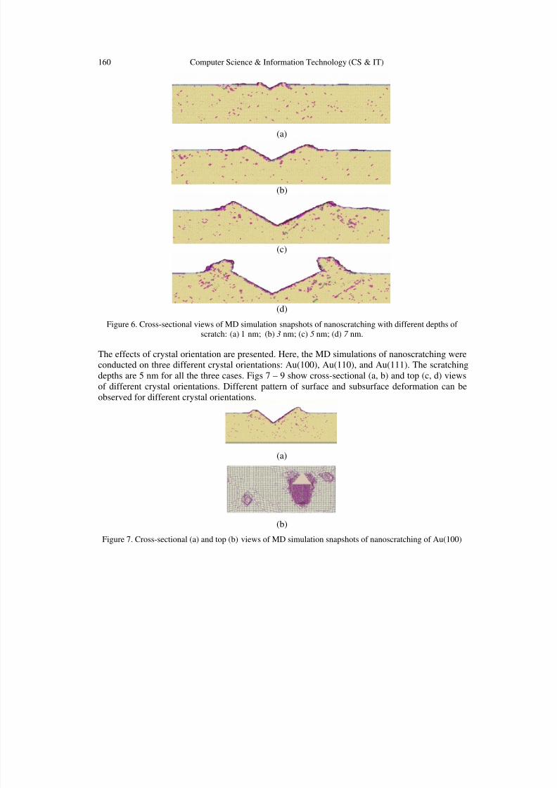
The effect of scratching depth on material deformation was investigated. MD simulations ofnanoscratching were conducted with scratch depths varying from 1 to7 nm. Top and cross-sectional views of MD simulation snapshots of nanoscratching at various scratching depths areshown in Figs. 5 - 6, respectively. As the scratching depth increases, the deformation is found topenetrate much deeper from the surface and the height of material pile-up also increases. Inaddition, more dislocation loops on the top surface can be observed. With increasing depth, thedislocations reach side boundaries sooner and re-enter from the opposite side. Some of thesepartial dislocations interact with other defects to form more defects on the top surface. Thisindicates that a larger computation domain is needed.
(a) (b)
(c) (d)Figure 5. Top view of MD simulation snapshots of nanoscratching with different depths of scratch: (a) 1
nm; (b) 3 nm; (c) 5 nm; (d) 7 nm.
8/10/2019 Molecular Dynamics Simulation Model of AFM-Based NanoMachining
http://slidepdf.com/reader/full/molecular-dynamics-simulation-model-of-afm-based-nanomachining 10/18
160 Computer Science & Information Technology (CS & IT)
(a)
(b)
(c)
(d)
Figure 6. Cross-sectional views of MD simulation snapshots of nanoscratching with different depths ofscratch: (a) 1 nm; (b) 3 nm; (c) 5 nm; (d) 7 nm.
The effects of crystal orientation are presented. Here, the MD simulations of nanoscratching wereconducted on three different crystal orientations: Au(100), Au(110), and Au(111). The scratchingdepths are 5 nm for all the three cases. Figs 7 – 9 show cross-sectional (a, b) and top (c, d) viewsof different crystal orientations. Different pattern of surface and subsurface deformation can beobserved for different crystal orientations.
(a)
(b)
Figure 7. Cross-sectional (a) and top (b) views of MD simulation snapshots of nanoscratching of Au(100)

8/10/2019 Molecular Dynamics Simulation Model of AFM-Based NanoMachining
http://slidepdf.com/reader/full/molecular-dynamics-simulation-model-of-afm-based-nanomachining 11/18
Computer Science & Information Technology (CS & IT) 161
(a)
(b)
Figure 8. Cross-sectional (a) and top (b) views of MD simulation snapshots of nanoscratching of Au(110)
(a)
(b)
Figure 9. Cross-sectional (a) and top (b) views of MD simulation snapshots of nanoscratching of Au(111)
Fig. 10 shows AFM image and cross-sectional profile of nanoindentation for different applied
forces, increasing from right to left: 65, 70, 75, 80, 85 µN. The AFM experiments were repeatedfor five times (five rows shown in Fig. 10). The indentation depths increase as the applied forcesincrease. The variation of indentation forces with depths of indentation at different tool tip speedsis shown in Figure 11. It can be observed that the indentation force increases as the depth ofindentation increases. The simulation results were compared with the experimental results. Due tothe limitation on computational time, it should be noted that the tool tip speeds used in this MDsimulation are a lot higher than those used in the experiment. The typical speed used in theexperiment is approximately 5-10 µm/s. Therefore, the effect of tool tip speed on the indentationforce is also investigated in this paper. It can be observed from Figure 11 that the indentationforce increases as the tool tip speed decreases. Since the tip speed plays an important role on theindentation force, the quantitative values of the indentation force obtained from MD simulationare not comparable to the experimental results. However, the increasing trends of indentationforce are the same for both simulation and experimental results. AFM experiments of
nanoindentation were also carried out to investigate the effect of the tip speed. Fig. 12 shows theexperimental results of AFM nanoindentation for different applied forces and different tip speeds.The tip speeds were increased from 1 to 10 µm/s from top to bottom rows. Fig. 12 (b) shows thecross-sectional profile of AFM nanoindentation. The blue line represents the cross-sectionalprofile for the tip speed of 1 µm/s. The red line represents the cross-sectional profile for the tipspeed of 10 µm/s. It can be seen from Fig. 12 (b) that the indentation depth increases as the tipspeed increases.

8/10/2019 Molecular Dynamics Simulation Model of AFM-Based NanoMachining
http://slidepdf.com/reader/full/molecular-dynamics-simulation-model-of-afm-based-nanomachining 12/18
162 Computer Science & Information Technology (CS & IT)
(a)
(b)
Figure 10. (a) AFM image of nanoindentation for different applied forces (increasing from right to left); (b)cross-sectional profile of AFM image
Figure 11. Variation in indentation forces with depths of indentation.
v=1 m/sv = 10 m/sExperimental resultsv = 10 m/s

8/10/2019 Molecular Dynamics Simulation Model of AFM-Based NanoMachining
http://slidepdf.com/reader/full/molecular-dynamics-simulation-model-of-afm-based-nanomachining 13/18
Computer Science & Information Technology (CS & IT) 163
(a) (b)
Figure 12. (a) AFM image of nanoindentation for different applied forces (increasing from right to left) andtip speeds (increasing from top to bottom); (b) cross-sectional profile of AFM image
Figure 13 shows the AFM experimental results of nanoscratching with five different depths,namely 20, 30, 40, 50, 60 nm (increasing from right to left). As can be seen from figure 13(b), thesurface roughness varies between 0 to 20 nm across the gold substrate. In order to obtain ameaningful result, the depths of scratch used in the experiments must be higher than 20 nm whichare ten times the depths used in the MD simulation. For this reason, the quantitative values, i.e.
forces, obtained from MD simulation are not comparable to the experimental results; only thequalitative values are discussed here. The height of the material pile-up along the scratch grooveis found to increase as the depth of cut increases in both MD simulation and AFM experiments.However, the material pile-up on the left side is observed to be higher than the right side which isdifferent from the MD simulation results. One possible explanation for the discrepancy may bethat the x-rotation of the AFM probe used in the experiment was set to 12 degree asrecommended by manufacturer. During the nanoscratching process, the pile-up material in frontof the tip increases, but not enough to form chip. Thus, no chip formation is detected in both MDsimulation and experiments for the observed depths of scratch.
(a) (b)
Figure 13. AFM experimental results of nano-scratching with five scratch depths of 20, 30, 40, 50, 60 nmincreasing from right to left: (a) AFM image of nanoscratching (b) cross-sectional profile
Figure 14 shows load-displacement curve for the case of gold material and diamond indenter tip.As the indentation depth of the diamond tip continues to increase, the load curve continues to goup and until its reaches a maximum depth. After reaching the specified maximum depth, the tipbegins to unload and return to it original position. The slope of the unloading curve at themaximum load is determined and used in the calculation of hardness and Young’s modulus in Eq.(8) and (10), respectively. Two different methods were used to calculate the contact area. In thefirst method, the contact area was calculated from the geometry of the indenter as a function ofthe contact depth, hc. In the second method, the contact area was estimated from the location ofdisplaced atoms at the interface between tip and sample. The material properties of diamondindenter used in the calculation are E i = 1140 GPa and νi = 0.07. Table 3 shows the values ofYoung’s modulus and hardness of gold obtained from the calculations.

8/10/2019 Molecular Dynamics Simulation Model of AFM-Based NanoMachining
http://slidepdf.com/reader/full/molecular-dynamics-simulation-model-of-afm-based-nanomachining 14/18
164 Computer Science & Information Technology (CS & IT)
Figure 14. Load-displacement curves for the case of gold material and diamond indenter tip.
Table 3. Young’s modulus and hardness of materials at nanoscale
Young’s modulus
(GPa)
Hardness
(GPa)
Method 1
Hardness
(GPa)
Method 2
235 113.56 98.13
Comparing to the macroscale properties, the Young’s modulus of gold is approximately 57-120GPa; while it was found to be 235 GPa from our calculation. The values of hardness obtainedfrom method 1 in our calculation is slightly larger than those obtained from method 2. Both
Young’s modulus and hardness in our analysis were about two to three times larger than those atthe macroscale. This discrepancy is a result of the scale differences. Bulk material typically hasconstant material properties regardless of its size, but size-dependent properties are oftenobserved at the nanoscale. Nanoscale material has a high surface area and a large fraction of theatoms are on its surface. This can give rise to size effects in material properties at the nanoscale.Moreover, the defect of the material such as grain boundaries and dislocations was different atdifferent scales. In addition, an assumption of perfect defect-free single-crystal material wasapplied in the MD simulation; while, in general, materials at macroscale were poly-crystalline andcontained several types of defects.
3. CONCLUSIONS
MD simulations of AFM-based nanoindentation and nanoscratching were conducted toinvestigate the effect of indentation and scratching depth, crystal orientation and tip speed.Material properties at the nanoscale were also extracted and compared with macroscopicproperties. Several types of defects, including vacancies and Shockley partial dislocation loops,could be observed during the simulation. With increasing depth of scratch, the dislocations reachside boundaries sooner and re-enter from the opposite side. Some of these partial dislocationsinteract with other defects to form more defects on the top surface. Due to the periodic boundarycondition applied to all the four side boundaries, the simulation domain should be large enough toavoid the re-entering of dislocations. For different crystal orientations, different pattern of surface
Loading
Unloading

8/10/2019 Molecular Dynamics Simulation Model of AFM-Based NanoMachining
http://slidepdf.com/reader/full/molecular-dynamics-simulation-model-of-afm-based-nanomachining 15/18
Computer Science & Information Technology (CS & IT) 165
and subsurface deformation can be observed. The effect of indentation depths and tip speeds wasinvestigated and found that indentation force increases as depth of indentation and tip speedincrease. Material properties, e.g. Young’s modulus and hardness, of the materials at thenanoscale are different from those at the macroscale. Hence, due to different material propertiesbetween nano- and macro-scale, materials at nanoscale are typically considered new types ofmaterial. As can be seen from the presented results, these machining parameters affected the finalnano-geometry in AFM-based nanomachining. The findings from this work can be applied to thefabrication of nanochannels/nano-fluidic devices. However, a more extensive experimental studyis necessary to better validate the computational models. This will be reported in our future work.
ACKNOWLEDGEMENTS
This research was supported in part by Lilly Endowment, Inc., through its support for the IndianaUniversity Pervasive Technology Institute, and in part by the Indiana METACyt Initiative. TheIndiana METACyt Initiative at IU is also supported in part by Lilly Endowment, Inc.
REFERENCES
[1] A.P. Malshe, K.P. Rajurkar, K.R. Virwani, C.R. Taylor, D.L. Bourell, G. Levy, M.M. Sundaram, J.A.McGeough, V. Kalyanasundaram and A.N. Samant, “Tip-based nanomanufacturing by electrical,chemical, mechanical and thermal processes,” CIRP Annals - Manufacturing Technology, Vol. 59, pp.628-651, 2010.
[2] A. C. Fischer-Cripps, Nanoindentation, Springer, New York, 2002.[3] A. N. Shipway, E. Katz and I Willner, “Nanoparticle Arrays on Surfaces for Electronic, Optical, and
sensor applications,” ChemPhysChem, Vol. 1(1), pp. 18–52, 2000.[4] M. Liu, N. A. Amro, C. S. Chow and G-Y Liu, “Production of Nanostructures of DNA on Surfaces,”
Nano Letters, Vol. 2(8), pp. 863–867, 2002.[5] P. Vettiger, M. Despont, U. Drechsler, U. Dürig, W. Häberle, M. I. Lutwyche, H. Rothuizen, R. Stutz,
R. Widmer and G. K. Binnig, “The ‘millipede’ – more than one thousand tips for future AFM datastorage,” IBM Journal of Research and Development , Vol. 44(3), pp. 323–340, 2000.
[6] C. R. Taylor, E. A. Stach, G. Salamo and A. P. Malshe, “Nanoscale dislocation Patterning by
Ultralow Load Indentation,” Applied Physics Letters, Vol. 87(7), 073108, 2005.[7] G. F. Zheng, F. Patolsky, Y. Cui, W. U. Wang and C. M. Lieber, “Multiplexed electrical detection ofcancer markers with nanowire sensor arrays,” Nature Biotechnology, Vol. 23(10), pp. 1294-1301,2005.
[8] X. Li, H. Gao, C. J. Murphy and K. K. Caswell, “Nanoindentation of silver nanowires,” Nano Letters,Vol. 3, pp.1495-1498, 2003.
[9] X. Li, P. Nardi, C. W. Baek, J. M. Kim and Y. K. Kim, “Direct nanomechanical machining of goldnanowires using a nanoindenter and an atomic force microscope,” Journal of Micromechanics and
Microengineering, Vol. 15, pp. 551-556, 2005.[10] Y. D. Yan, T. Sun, X. S. Zhao, Z. J. Hu and S. Dong, “Fabrication of microstructures on the surface
of a micro/hollow target ball by AFM,” Journal of Micromechanics and Microengineering, Vol. 18,035002, 2008.
[11] Y. J. Chen, J. H. Hsu and H. N. Lin, “Fabrication of metal nanowires by atomic force microscopynanoscratching and lift-off process,” Nanotechnology, Vol. 16, pp. 1112-1115, 2005.
[12] Y. T. Mao, K. C. Kuo, C. E. Tseng, J. Y. Huang, Y. C. Lai, J. Y. Yen, C. K. Lee and W. L. Chuang,“Research on three dimensional machining effects using atomic force microscope,” Review of
Scientific Instruments, Vol. 80, 065105, 2009.[13] T. Fang, C. Weng and J. Chang, “Machining characterization of nano-lithography process using
atomic force microscopy,” Nanotechnology, Vol. 11, pp. 181-187, 2000.[14] S. Diegoli, C. A. E. Hamlett, S. J. Leigh, P. M. Mendes and J. A. Preece, “Engineering nanostructures
at surfaces using nanolithography,” Proceedings of the Institution of Mechanical Engineers, Part G:
Journal of Aerospace Engineering, Vol. 221(4), pp. 589-629, 2007.[15] T. Sun, Y. D. Yan, J. F. Xia, S. Dong, Y. C. Liang and K. Cheng, “Research on micro machining
using AFM diamond tip,” Key Engineering Materials, Vols. 259-260, pp. 577-581, 2004.

8/10/2019 Molecular Dynamics Simulation Model of AFM-Based NanoMachining
http://slidepdf.com/reader/full/molecular-dynamics-simulation-model-of-afm-based-nanomachining 16/18
166 Computer Science & Information Technology (CS & IT)
[16] J. C. Huang, C. L. Li, and J. W. Lee, “The Study of Nanoscratch and Nanomachining on HardMultilayer Thin Films Using Atomic Force Microscope,” Scanning, Vol. 34, pp. 51-59, 2012.
[17] Y. Yan, T. Sun, Y. Liang and S. Dong, “Investigation on AFM-based micro/nano-CNC machiningsystem,” International Journal of Machine Tools and Manufacture, Vol. 47, pp. 1651-1659, 2007.
[18] F. Zhang, H. Zhang, Y. Yan and J. Wang, “ Research on nano-scale material removal process usingatomic force microscopy,” Key Engineering Materials, Vols. 359-360, pp. 269-273, 2008.
[19] H. Zhang, J. Kuai and F. Zhang, “Minimum thickness of cut in nanomachining using atomic forcemicroscopy,” 2010 International Conference on E-Product E-Service and E-Entertainment (ICEEE) ,Henan, China, November 7-9, 2010.
[20] A. A. Tseng, J. Shirakashi, S. Nishimura, K. Miyashita and Z. Li, “Nanomachining of permalloy forfabricating nanoscale ferromagnetic structures using atomic force microscopy,” Journal of
Nanoscience and Nanotechnology, Vol. 10, pp. 456-466, 2010.[21] Z. Q. Wang, N. D. Jiao, S. Tung and Z. L. Dong, “Atomic force microscopy-based repeated
machining theory for nanochannels on silicon oxide surfaces,” Applied Surface Science, Vol. 257, pp.3627-3631, 2011.
[22] W. C. D. Cheong and L. C. Zhang, “Molecular dynamics simulation of phase transformations insilicon monocrystals due to nano-indentation,” Nanotechnology, Vol. 11, pp. 173-180, 2000.
[23] R. Komanduri, N. Chandrasekaran and L.M. Raff, “MD simulation of indentation and scratching ofsingle crystal aluminum,” Wear , Vol. 240, pp. 113-143, 2000.
[24] D. Christopher, R. Smith and A. Richter, “Atomistic modelling of nanoindentation in iron and silver,”
Nanotechnology, Vol. 12, pp. 372-383, 2001.[25] T. Fang, C. Weng and J. Chang, “Molecular dynamics analysis of temperature effects onnanoindentation measurement,” Material Science and Engineering, Vol. A357, pp. 7-12, 2003.
[26] X. M. Liu, Z. L. Liu and Y G Wei, “Nanoscale Friction Behavior of the Ni-film/substrate systemunder scratching using MD simulation,” Tribology Letters Vol. 46, pp. 167-178, 2012.
[27] A. Gannepalli and S. K. Mallapragada, “Molecular dynamics studies of plastic deformation duringsilicon nanoindentation,” Nanotechnology, Vol. 12, pp. 250-257, 2001.
[28] I. Salehinia, S.K. Lawrence and D.F. Bahr, “The effect of crystal orientation on the stochasticbehavior of dislocation nucleation and multiplication during nanoindentation,” Acta Materialia, Vol.61, pp. 1421-1431, 2013.
[29] C. F. Sanz-Navarro, S. D. Kenny and R. Smith, “Atomistic simulations of structural transformationsof silicon surfaces under nanoindentation,” Nanotechnology, Vol. 15, pp. 692-697, 2004.
[30] T. Akabane, Y. Sasajima and J. Onuki, “Computer simulation of silicon nanoscratch test,” Materials
Transactions, Vol. 47, pp. 1090-1097, 2006.
[31] H. Okabe, T. Tsumura, J. Shimizu, L. Zhou and H. Eda, “Experimental and Simulation Research onInfluence of Temperature on Nano-Scratching Process of Silicon Wafer,” Key Engineering Materials,Vol. 329, pp. 379-384, 2007.
[32] T. Fang, W. Chang and C. Weng, “Nanoindentation and nanomachining characteristics of gold andplatinum thin films,” Materials Science and Engineering A, Vol. 430, pp. 332-340, 2006.
[33] T. Fang and C. Weng, “Three-dimensional molecular dynamics analysis of processing using a pin toolon the atomic scale,” Nanotechnology, Vol. 11, pp. 148-153, 2000.
[34] T. Fang, C. Weng, and J. Chang, “Molecular dynamics simulation of nano-lithography process usingatomic force microscopy,” Surface Science, Vol. 501, pp. 138-147, 2002.
[35] Y. Yan, T. Sun, S. Dong and Y. Liang, “Study on effects of the feed on AFM-based nano-scratchingprocess using MD simulation,” Computational Materials Science, Vol. 40, pp. 1-5, 2007.
[36] H. Yu, J. B. Adams and L. G. Hector Jr, “Molecular dynamics simulation of high-speednanoindentation,” Modeling and Simulation in Materials Science and Engineering, Vol. 10, pp. 319-329, 2002.
[37] S. Jun, Y. Lee, S. Kim and S. Im, “Large-scale molecular dynamics simulations of Al(111)nanoscratching,” Nanotechnology, Vol. 15, pp. 1169-1174, 2004.
[38] Y. Lee, J. Park, S. Kim, S. Jun and S. Im, “Atomistic simulations of incipient plasticity under Al(111)nanoindentation,” Mechanics of Materials, Vol. 37, pp. 1035-1048, 2005.
[39] D. Mulliah, D. Christopher, S. D. Kenny and R. Smith, “Nanoscratching of silver (100) with adiamond tip,” Nuclear Instruments and Methods in Physics Research B, Vol. 202, pp. 294-299, 2003.
[40] D. Mulliah, S. D. Kenny, R. Smith and C. F. Sanz-Navarro, “Molecular dynamics simulations ofnanoscratching of silver (100),” Nanotechnology, Vol. 15, pp. 243-249, 2004.
[41] R. Smith, D. Cristopher and S. D. Kenny, “Defect generation and pileup of atoms duringnanoindentation of Fe single crystals,” Physical Review B, Vol. 67, 245405, 2003.

8/10/2019 Molecular Dynamics Simulation Model of AFM-Based NanoMachining
http://slidepdf.com/reader/full/molecular-dynamics-simulation-model-of-afm-based-nanomachining 17/18
Computer Science & Information Technology (CS & IT) 167
[42] C. Lu, Y. Gao, G. Y. Deng, G. Michal, N. N. Huynh, X. H. Liu and A. K. Tieu, “Atomic-scaleanisotropy of nanoscratch behavior of single crystal iron,” Wear , Vol. 267, pp. 1961-1966, 2009.
[43] Z. Lin, J. Huang and Y. Jeng, “3D nano-scale cutting model for nickel material,” Journal of Materials
Processing Technology, Vol. 192-193, pp. 27-36, 2007.[44] Y. Gao, C. Lu, N. N. Huynh, G. Michal, H. T. Zhu and A. K. Tieu, “Molecular dynamics simulation
of effect of indenter shape on nanoscratch of Ni,” Wear , Vol. 267, pp. 1998-2002, 2009.
[45] I. Gheewala, R. Smith and S. D. Kenny, “Nanoindentation and nanoscratching of rutile and anataseTiO2 studied using molecular dynamics simulations,” Journal of Physics: Condensed Matter , Vol. 20,354010, 2008.
[46] Y. Liang, J. Chen, M. Chen, D. Song and Q Bai, “Three-dimensional molecular dynamics simulationof nanostructure for reciprocating nanomachining process,” Journal of Vacuum Science and
Technology B, Vol. 27, pp. 1536-1542, 2009.[47] J. Chen, Y. Liang, Q. Bai, Y. Tang and M. Chen, “Mechanism of material removal and the generation
of defects by MD analysis in three-dimensional simulation in abrasive processes,” Key Engineering
Materials, Vol. 359-360, pp. 6-10, 2008.[48] Z. Lin and J. Huang, “A study of the estimation method of the cutting force for a conical tool under
nanoscale depth of cut by molecular dynamics,” Nanotechnology, Vol. 19, 11570, 2008.[49] D. Mulliah, S. D. Kenny, E. McGee, R. Smith, A. Richter and B. Wolf, “Atomistic modeling of
ploughing friction in silver, iron and silicon,” Nanotechnology, Vol. 17, pp. 1807-1818, 2006.[50] R. Promyoo, H. El-Mounayri, and A. Martini, “AFM-Based Nanomachining for Nano-fabrication
Processes: MD Simulation and AFM Experimental Verification,” ASME International ManufacturingScience & Engineering Conference, Erie, PA, October 2010.
[51] R. Promyoo, H. El-Mounayri, K. Varahramyan, and A. Martini, “Molecular Dynamics Simulation ofAFM-Based Nanomachining Processes,” ASME International Manufacturing Science & Engineering
Conference, Corvallis, OR, June 13 – 17, 2011.[52] R. Promyoo, H. El-Mounayri, and K. Varahramyan, “AFM-Based Manufacturing for Nano-
fabrication Processes,” TSME International Conference on Mechanical Engineering, Krabi, Thailand,October 2011.
[53] R. Promyoo, H. El-Mounayri, and K. Varahramyan, “AFM-Based Nanoindentation Process: AComparative Study,” ASME International Manufacturing Science & Engineering Conference, NorteDame, IN, June 4-8, 2012.
[54] R. Promyoo, H. El-Mounayri, K. Varahramyan, and V. Kumar, “AFM-Based Nanofabrication:Modeling, Simulation, and Experimental Verification,” ASME International Manufacturing Science
& Engineering Conference, Madison, WI, June 10 – 14, 2013.
[55] R. Promyoo, H. El-Mounayri, and K. Varahramyan, “AFM-based nanoindentation using a 3Dmolecular dynamics simulation model,” Journal of Materials Science and Engineering A, Vol. 3(6),pp. 369-381, 2013.
[56] B. J. Alder and T. E. Wainwright, 1959, "Studies in molecular dynamics. I. General method," Journal
of Chemical Physics, Vol. 31, pp. 459-466, 1959.[57] B. J. Alder and T. E. Wainwright, "Studies in molecular dynamics. II. Behavior of a small number of
elastic spheres," Journal of Chemical Physics, Vol. 33, pp. 1439-1451, 1960.[58] R. Komanduri and L. M. Raff, “A review on the molecular dynamics simulation of machining at the
atomic scale,” Proceedings Institution of Mechanical Engineers, Vol. 215 (B), pp. 1639-1672, 2001.[59] S. J. Plimpton, S. J., “Fast parallel algorithms for short-range molecular dynamics,” Journal of
Computational Physics, Vol. 117, pp. 1-19, 1995.[60] S. J. Plimpton, R. Pollock and M. Stevens, “Particle-mesh Ewald and rRESPA for parallel molecular
dynamics simulations,” Proc of the Eighth SIAM Conference on Parallel Processing for Scientific
Computing, Minneapolis, MN.[61] P. Walsh, R. K. Kalia, A. Nakano and P. Vashishta, “Amorphization and anisotropic fracture
dynamics during nanoindentation of silicon nitride: A multimillion atom molecular dynamics study,” Applied Physics Letters, Vol.77, pp.4332-4334, 2000.
[62] M. S. Daw and M. I. Baskes, “Embedded-atom method: Derivation and application to impurities,surfaces, and other defects in metals,” Physical Review B, Vol. 29, pp. 6443-6453, 1984.
[63] P. M. Morse, “Diatomic molecules according to the wave mechanics II vibrational levels,” Physical
Review, Vol. 34, pp. 57-64, 1929.[64] I. M. Torrens, Interatomic potentials, Academic, New York, 1972.

8/10/2019 Molecular Dynamics Simulation Model of AFM-Based NanoMachining
http://slidepdf.com/reader/full/molecular-dynamics-simulation-model-of-afm-based-nanomachining 18/18
168 Computer Science & Information Technology (CS & IT)
[65] W.C. Oliver, G.M. Pharr, “Measurement of hardness and elastic modulus by instrumentedindentation: Advances in understanding and refinements to methodology,” Journal of Material
Research, Vol. 19, pp. 3-20, 2004.[66] http://rt.uits.iu.edu/bigred2/index.php[67] J. Li, “AtomEye: an efficient atomistic configuration viewer,” Modeling and Simulation in Materials
Science and Engineering, Vol. 11, pp. 173-177, 2003.