Embed Size (px)
Citation preview

Molecular Doping Processes inOrganic Semiconductors investigated
by Photoelectron Spectroscopy
Dissertationzur Erlangung des wissenschaftlichen Grades
Dr. rer. nat.
vorgelegt von
Max L. Tietzegeboren am 08.02.1986 in Dresden
Institut für Angewandte Photophysik der TU DresdenDresden 2014

Eingereicht am 30.05.2014
1. Gutachter: Prof. Dr. Karl Leo2. Gutachter: Prof. Dr. Torsten Fritz

Abstract
Molecular doping is a key technique for realizing high efficient organic light-emitting diodes (OLEDs)and photovoltaics (OPV). Furthermore, its most recent application in organic field-effect transistors(OFETs) marks a milestone on the roadmap towards flexible organic CMOS technology. However,in contrast to silicon based devices, the understanding of the fundamental processes of moleculardoping is still controversially discussed. This work aims at the detailed analysis of the moleculardoping process by employing Photoelectron spectroscopy (PES) on various doped thin-films pre-pared by co-evaporation in vacuum. Here, the focus is on explanation of the experimental findingsby a statistical description in order to contribute to the fundamental understanding of the dopingmechanism.First, the Fermi level shifts in thin-films of the common hole transport materials MeO-TPD, ZnPc,and pentacene p-doped by the acceptors C60F36 and F6-TCNNQ are studied. The precise control ofmolar doping ratios as low as 10−5 is demonstrated, allowing analysis of the doping properties in amuch broader range as previously accessible. Characteristic kinks and slopes in the Fermi level vs.doping concentration diagrams are found. Furthermore, the doping efficiency is found to decreasewith increasing doping concentrations to just a few percent at molar ratios above 0.1. By numeri-cally solving the charge neutrality equation using a classical semiconductor physics approach, thesefindings are explained by trap-limitation, dopant saturation, and reserve regimes as known frominorganic semiconductor physics. Using the example of p-doped MeO-TPD thin-films, it is finallydemonstrated that the density of deep gap states depends on the purity degree of the host material.Similar studies are conducted on thin-films of C60, ZnPc, and pentacene n-doped by the di-metalcomplex W2(hpp)4. The corresponding Fermi level plots possess also host material specific kinksand slopes, which however, can be explained by application of the statistical doping description andassuming just dopant saturation and trap-limitation. Furthermore, it is demonstrated that electrontraps with defined density can intentionally be introduced in pentacene by co-evaporation of C60
and gradually filled-up by n-doping with W2(hpp)4.In contrast to p-dopants, the highly efficient n-dopant W2(hpp)4 is prone to degradation in air dueto its low IP of just 2.4 eV. Therefore, the degradation of pure films of W2(hpp)4 as well as ofn-doped films applying various host materials is studied under air exposure by conductivity mea-surements and PES. An unexpected (partial) passivation of W2(hpp)4 molecules against oxidationis found, however, this effect is identified to depend on the energy levels of the used host material.This finding is explained by a down-shift of the W2(hpp)4 energy levels upon charge transfer to ahost material with deeper lying energy levels and thus allows for new conclusions on the relativealignment of the energy levels of dopant and host molecules in doped films in general.The maximum open-circuit voltage VOC of BHJ solar cells is limited by the effective HOMO(donor)-LUMO(acceptor) gap of the photo-active absorber blend. Therefore, the relative energy levelswithin ZnPc:C60 blend layers are furthermore investigated by PES, identifying an increase of theHOMO(ZnPc)-LUMO(C60) gap by 0.25 eV when varying the blend stoichiometry from 6:1 to 1:6.The trend in this gap correlates with observed changes in VOC of respective BHJ solar cells aswell as with measured charge transfer energies. As physical origins for the changed energy lev-els, a suppressed crystallization of the C60 phase due to presence of donor molecules as well asconcentration-dependent growth modes of the ZnPc phase are discussed.
iii

iv

Kurzfassung
Molekulare Dotierung ist eine Schlüsseltechnologie zur Realisierung hoch effizienter organischerLeuchtdioden (OLEDs) und Photovoltaik (OPV). Außerdem markiert ihr jüngster Einsatz in organ-ischen Feldeffekt Transistoren (OFETs) einen Meilenstein auf dem Weg zur flexiblen organischenCMOS Technologie. Im Gegensatz zu Silizium werden die grundlegenden Prozesse der molekularenDotierung aber noch immer kontrovers diskutiert. Ziel dieser Arbeit ist es, mittels PhotoelektronenSpektroskopie die Prozesse der Dotierung in vakuum-verdampften organischen Dünnschichten imDetail zu untersuchen und die experimentellen Ergebnisse mit einer statistischen Beschreibung desDotierprozesses zu erklären.Zuerst wird die Verschiebung des Fermi-Niveaus in p-dotierten Dünnschichten der gängigen Lochtrans-port Materialien MeO-TPD, ZnPc und Pentazen untersucht. Als Akzeptor-Moleküle kommen hier-bei C60F36 und F6-TCNNQ zum Einsatz, wobei das präzise Einstellen molarer Dotierkonzentratio-nen von bis zu 10−5 demonstriert wird. Dies ermöglicht die Analyse des Dotierprozesses über einendeutlich weiteren Bereich als zuvor zugänglich. Die gemessenen Fermi-Niveau vs. Dotierkonzentra-tion Kurven zeigen verschiedene Bereiche mit charakteristischen Knicken und Anstiegen. Außer-dem wird gezeigt, dass die Dotiereffizienz mit steigender Konzentration abfällt und oberhalb vonmolaren Dotierverhältnissen von 0.1 nur noch wenige Prozent beträgt. Diese Ergebnisse könnenmittels numerischer Lösung der Neutralitätsgleichung unter Verwendung klassischer Halbleitergle-ichungen erklärt werden. Insbesondere können die bekannten Bereiche der Begrenzung durch Fall-enzustände, Störstellen-Erschöpfung und Reserve den Messkurven zugeordnet werden. Am Beispielvon p-dotiertem MeO-TPD kann schließlich gezeigt werden, dass die Dichte an tiefen Fallzuständenmit der Reinheit des Wirtsmaterials korreliert.Vergleichbare Untersuchungen wurden weiterhin an n-dotierten C60, ZnPc und Pentazen Schichtenmit dem Dotanten-Molekül W2(hpp)4 durchgeführt. Die entsprechenden Fermi-Niveau Graphenzeigen ebenfalls für das Material charakteristische Knicke und Anstiege und können unter Annahmevon Fallen-Begrenzung und Dotantenerschöpfung mit dem statistischen Modell erklärt werden.Außerdem wird gezeigt, dass Elektronenfallen definierter Dichte in Pentazen durch Koverdamp-fung von C60 gezielt eingebaut und graduell durch n-Dotierung mit W2(hpp)4 aufgefüllt werdenkönnen.Im Gegensatz zu den p-Dotanten ist der effiziente n-Dotant W2(hpp)4 aufgrund seines geringenIP von nur 2.4 eV anfällig gegenüber Degradation an Luft. Daher wird die Degradation reinerW2(hpp)4 sowie verschiedener n-dotierter Schichten unter Luftaussetzung mittels Leitfähigkeits undPES Messungen untersucht. Eine unerwartete (teilweise) Passivierung von W2(hpp)4 Molekülen,die jedoch von den Energieniveaus des verwendeten Wirtsmaterials abhängt, konnte festgestellt wer-den. Dieses Ergebnis wird durch das Herunterschieben der W2(hpp)4 Energieniveaus aufgrund vonLadungstransfer zu einem Wirt mit tiefer liegenden Energieniveaus erklärt. Dieser Befund liefertneue Erkenntnisse bzgl. des relativen Energieniveau-Alignments von Dotanten and Wirt Molekülenin dotierten Schichten im Allgemeinen.Die maximale Klemmenspannung VOC organischer BHJ Solarzellen ist durch das effektiveHOMO(Donator)-LUMO(Akzeptor) gap der photoaktiven Schicht begrenzt. Daher wird weiterhindas relative Energieniveau-Alignment in ZnPc:C60 Mischschichten untersucht, wobei ein Anstiegdes effektiven HOMO(ZnPc)-LUMO(C60) gaps von 0.25 eV unter Variation der Stöchiometrie von
v

6:1 bis zu 1:6 bestimmt wird. Diese gefundene Tendenz korreliert mit gemessenen SpannungenVOC entsprechender BHJ Solarzellen sowie Ladungstransfer-Komplex Energien. Als physikalischeUrsache für die Änderungen in den Energieniveaus wird eine durch die Donatorphase unterdrückteKristallisation von C60 sowie das konzentrationsabhänigige Wachstum der ZnPc Phase diskutiert.
vi
Publications
Articles
A1. J. Meiss, A. Merten, M. Hein, C. Schünemann, S. Schäfer, M. Tietze, C. Uhrich, M. Pfeiffer, K.Leo, and M. Riede: Fluorinated Zinc Phthalocyanine as Donor for Efficient Vacuum-DepositedOrganic Solar Cells, Advanced Functional Materials 22, 405-414 (2012).doi:10.1002/adfm.201101799
A2. M. Tietze, L. Burtone, B. Lüssen, M. Riede, and K. Leo: Fermi level shift and doping efficiencyin p-doped small molecule organic semiconductors: A photoelectron spectroscopy and theoreticalstudy, Physical Review B 86, 035320 (2012). doi:10.1103/PhysRevB.86.035320.
A3. J. Widmer, M. Tietze, M. Riede, and K. Leo: Open-Circuit Voltage and Effective Gap ofOrganic Solar Cells, Advanced Functional Materials 23, 5814-5821 (2013).doi:10.1002/adfm.201301048.
A4. M. Tietze, W. Tress, S. Pfützner, M. Riede, K. Vandewal, S. Olthof, P. Schulz, A. Kahn, andK. Leo: Correlation of the open-circuit voltage and the energy levels in zinc-phthalocyanine:C60
bulk heterojunction solar cells with varied mixing ratio, Physical Review B 88, 085119 (2013).doi:10.1103/PhysRevB.88.085119.
A5. M. Tietze, K. Leo, and B. Lüssem: Quantification of deep hole-trap filling by molecular p-doping: Dependence on the host material purity, Organic Electronics 14, 2348-2352 (2013).doi:10.1016/j.orgel.2013.05.036.
A6. M. Tietze, F. Wölzel, T. Menke, A. Fischer, B. Lüssem, and K. Leo: Self-passivation ofmolecular n-type doping during air exposure using a highly efficient air-instable dopant, physicastatus solidi (a) 210, 2188-2198 (2013). doi:10.1002/pssa.201330049.
A7. B. Lüssem, M. Tietze, H. Kleemann, C. Hoßbach, J. W. Bartha, A. Zakhidov, and K. Leo:Doped Organic Transistors: Inversion and Depletion Regime, Nature Communications 4, 2775(2013). doi:10.1038/ncomms3775.
A8. P. Pahner, H. Kleemann, L. Burtone, M. Tietze, J. Fischer, K. Leo, and B. Lüssem: PentaceneSchottky diodes studied by impedance spectroscopy: Doping properties and trap response, Phys-ical Review B 88, 195205 (2013). doi:10.1103/PhysRevB.88.195205.
vii

A9. A. Fischer, T. Koprucki, K. Gärtner, M. Tietze, J. Brückner, B. Lüssem, K. Leo, A. Glitzky,and R. Scholz: Feel the heat: Nonlinear electrothermal feedback in Organic LEDs, AdvancedFunctional Materials, in press (2014). doi:10.1002/adfm.201303066.
A10. E. Siebert-Heinze, V. G. Lyssenko, M. Tietze, J. Fischer, R. Brückner, T. Menke, K. Leo, andM. Riede: Electroabsorption studies of organic p-i-n solar cells: Increase of the built-in voltageby higher doping concentration in the hole transport layer, Organic Electronics 15, 563-568(2014). doi:10.1016/j.orgel.2013.12.009.
A11. M. Hein, A. Zakhidov, B. Lüssem, J. Jankowski, M. Tietze, M. Riede, and K. Leo: Moleculardoping for control of gate bias stress in organic thin film transistors, Applied Physics Letters104, 013507 (2014). doi:10.1063/1.4861168.
A12. E. Siebert-Heinze, V. G. Lyssenko, J. Fischer, M. Tietze, R. Brückner, M. Schwarze, K.Vandewal, D. Ray, M. Riede, and K. Leo: Built-in voltage of organic bulk heterojunctionp-i-n solar cells measured by electroabsorption spectrosopy, AIP Advances 4, 047134 (2014).doi:10.1063/1.4861168.
A13. C. Poelking, M. Tietze, C. Elschner, K. Leo, B. Baumeier, and D. Andrienko: Decisive Roleof Long-Range Interactions and Molecular Order at Organic Interfaces, submitted.
A14. I. Rabelo de Moraes, S. Scholz, M. Hermenau, M. Tietze, M. Gather, and K. Leo: Impact oftemperature on the power efficiency of organic light emitting diodes, submitted.
A15. M. Tietze, P. Pahner, K. Leo, and B. Lüssem: Doped Organic Semiconductors: Trap-filling,Impurity Saturation and Reserve Regimes, in preparation.
A16. M. Tietze, A. Fischer, S. Pfützner, J. Blochwitz-Nimoth, B. Lüssem, and K. Leo: Self-passivation of molecular n-type doping: Dependence on the host material, in preparation.
A17. J. Fischer, J. Widmer, H. Kleemann, M. Tietze, W. Tress, K. Leo, and M. Riede: ChargeTransport Properties of Organic Bulk Heterojunction Layers studied in p-i-p Devices, in prepa-ration.
A18. P. Pahner, K. Schmidt, M. Tietze, M. Schwarze, K. Leo, and B. Lüssem: Temperature activatedtrap response in p-doped zinc-phthalocynanine, in preparation.
Book Chapters
B1. F. Löser, M. Tietze, B. Lüssem, and J. Blochwitz-Nimoth: Chapter 9: Conductivity Doping inFundamentals of High-Efficiency OLEDs - Basic Science to Manufacturing of Organic Light-Emitting Diodes, edited by D. J. Gaspar and E. Polikarpov, 1. Edition (2014).ISBN-13: 978-1466515185.
viii

Conference Contributions (presenting Author only)
C1. S. Pfützner, M. Tietze, L. Burtone, B. Lüssem, M. Riede, and K. Leo: Dependency of VOC onmixing ratio in BHJ solar cells, DPG Frühjahrstagung, 14th March 2011, Dresden (Talk).
C2. M. Tietze, L. Burtone, B. Lüssem, M. Riede, and K. Leo: Molecular doping processes inorganic semiconductors: An experimental and numerical study, SPIE Photonics West, 14th
August 2012, San Diego, CA-US (Talk).
C3. M. Tietze, F. Wölzel, T. Menke, A. Fischer, B. Lüssem and K. Leo: Self-passivation of molec-ular n-type doping during air-exposure, DPG Frühjahrstagung, 13th March 2013, Regensburg(Talk).
C4. M. Tietze, P. Pahner, B. Lüssem, and K. Leo: Molecular doping: Achieving high dopingefficiencies in p- and n-type doped Pentacene and ZnPc, MRS spring meeting, 2th April 2013,San Francisco, CA-US (Poster).
C5. M. Tietze, C. Elschner, F. Holzmüller, Michael Zopf, Roland Fitzner, Peter Bäuerle, ChristianKoerner, and K. Leo: Morphology - Efficiency Correlation in DCV5T:C60 BHJ Solar Cellscontrolled by Substrate Heating and Side Chain Variation, MRS spring meeting, 24th April2014, San Francisco, CA-US (Poster).
Seminar Talks
S1. M. Tietze, L. Burtone, B. Lüssen, M. Riede, and K. Leo: Molecular doping processes in organicsemiconductors, Bao research group, 20th Aug. 2012, Stanford University, Stanford, CA-US.
ix

x

Contents
1 Introduction 1
2 Fundamentals of Molecular Semiconductors 52.1 Molecules with Delocalized π-Electron Systems . . . . . . . . . . . . . . . . . . . . . 52.2 From Single Molecules to Molecular Solids . . . . . . . . . . . . . . . . . . . . . . . . 92.3 Single Charges in Molecular Solids: Charge Transport Properties . . . . . . . . . . . 13
2.3.1 Band-like and Polaron Transport in Organic Crystals . . . . . . . . . . . . . 142.3.2 Static Disorder and Hopping Transport in Amorphous Films . . . . . . . . . 15
2.4 Excited Molecules: Optical Properties and Excitons . . . . . . . . . . . . . . . . . . 202.5 Energy Level Alignment at Interfaces . . . . . . . . . . . . . . . . . . . . . . . . . . . 22
2.5.1 Metal/Organic Interfaces . . . . . . . . . . . . . . . . . . . . . . . . . . . . . 232.5.2 Organic/Organic Interfaces . . . . . . . . . . . . . . . . . . . . . . . . . . . . 27
3 Molecular Doping 293.1 Introduction to Molecular Doping: Terms and Definitions . . . . . . . . . . . . . . . 293.2 Historical Development of Dopant Compounds . . . . . . . . . . . . . . . . . . . . . 31
3.2.1 Early Doping Work with Metals and Gases . . . . . . . . . . . . . . . . . . . 313.2.2 Organic Molecules as Conductivity Dopants . . . . . . . . . . . . . . . . . . . 313.2.3 Precursor Molecules . . . . . . . . . . . . . . . . . . . . . . . . . . . . . . . . 323.2.4 Electrical Doping of Polymers . . . . . . . . . . . . . . . . . . . . . . . . . . . 34
3.3 Prevailing Theories on the Molecular Doping Process . . . . . . . . . . . . . . . . . . 353.4 Application to Functional Organic Devices . . . . . . . . . . . . . . . . . . . . . . . . 46
3.4.1 Schottky Contacts . . . . . . . . . . . . . . . . . . . . . . . . . . . . . . . . . 463.4.2 Organic p-i-n Diodes and Solar Cells . . . . . . . . . . . . . . . . . . . . . . . 50
4 Experimental and Materials 534.1 Sample Preparation . . . . . . . . . . . . . . . . . . . . . . . . . . . . . . . . . . . . 534.2 Material Properties . . . . . . . . . . . . . . . . . . . . . . . . . . . . . . . . . . . . . 55
4.2.1 Host Materials . . . . . . . . . . . . . . . . . . . . . . . . . . . . . . . . . . . 554.2.2 Dopant Molecules . . . . . . . . . . . . . . . . . . . . . . . . . . . . . . . . . 584.2.3 Transport Materials applied in Solar Cells . . . . . . . . . . . . . . . . . . . . 58
4.3 Fundamentals of Photoelectron Spectroscopy . . . . . . . . . . . . . . . . . . . . . . 594.3.1 Introduction to the Theory of the Photoelectron Emission Process . . . . . . 59
xi

4.3.2 Details of the Experimental UPS/XPS Setup . . . . . . . . . . . . . . . . . . 614.3.3 Principles of UPS/XPS Experiments and Data Analysis . . . . . . . . . . . . 64
4.4 Other Characterization Techniques . . . . . . . . . . . . . . . . . . . . . . . . . . . . 684.4.1 Conductivity . . . . . . . . . . . . . . . . . . . . . . . . . . . . . . . . . . . . 684.4.2 Impedance Spectroscopy . . . . . . . . . . . . . . . . . . . . . . . . . . . . . . 684.4.3 Laser Desorption Ionization - Time of Flight - Mass Spectroscopy . . . . . . . 694.4.4 Solar Cell Characterization . . . . . . . . . . . . . . . . . . . . . . . . . . . . 694.4.5 Grazing incidence X-Ray Diffraction . . . . . . . . . . . . . . . . . . . . . . . 694.4.6 Fourier-Transform Photocurrent Spectroscopy . . . . . . . . . . . . . . . . . . 70
5 Investigations on Molecular p-Doping 715.1 P-Type Doping of MeO-TPD by C60F36 and F6-TCNNQ . . . . . . . . . . . . . . . 71
5.1.1 Fermi Level Position versus Doping Concentration . . . . . . . . . . . . . . . 715.1.2 Resolving Depletion Layer Thicknesses: Estimating the Doping Efficiency . . 745.1.3 Comparison to Mott-Schottky Analysis . . . . . . . . . . . . . . . . . . . . . 78
5.2 Development of a Statistical Doping Model . . . . . . . . . . . . . . . . . . . . . . . 825.2.1 Basic Calculations . . . . . . . . . . . . . . . . . . . . . . . . . . . . . . . . . 835.2.2 Definition of the Fermi Level Position . . . . . . . . . . . . . . . . . . . . . . 915.2.3 Application to p-doped MeO-TPD: Conclusion on the Molecular Doping Process 935.2.4 Application to p-doped unpurified MeO-TPD: Conclusion on Trap States . . 97
5.3 Analysis of p-Type Doping of Pentacene and ZnPc . . . . . . . . . . . . . . . . . . . 1025.3.1 High Resolution UPS on undoped Thin-Films . . . . . . . . . . . . . . . . . . 1025.3.2 Fermi Level Shift in ultra-low p-doped Thin-Films . . . . . . . . . . . . . . . 1065.3.3 Doping Efficiency: Qualitative Evidence for Impurity Reserve and Saturation
Regimes . . . . . . . . . . . . . . . . . . . . . . . . . . . . . . . . . . . . . . . 1085.4 Summary . . . . . . . . . . . . . . . . . . . . . . . . . . . . . . . . . . . . . . . . . . 118
6 Investigations on Molecular n-Doping 1196.1 N-Type Doping by the Molecular Di-Metal Complex W2(hpp)4 . . . . . . . . . . . . 119
6.1.1 IPES on Pentacene, ZnPc, and C60 Thin-Films: Gap Determination . . . . . 1196.1.2 Fermi Level Shift in Pentacene, ZnPc, and C60 Thin-Films . . . . . . . . . . 121
6.2 Self-Passivation of Molecular n-Type Doping . . . . . . . . . . . . . . . . . . . . . . 1256.2.1 Passivation of W2(hpp)4 in C60 . . . . . . . . . . . . . . . . . . . . . . . . . . 1256.2.2 Passivation of W2(hpp)4 in C60: Improvement by intrinsic Cover Layer . . . 1376.2.3 Host Material Variation . . . . . . . . . . . . . . . . . . . . . . . . . . . . . . 141
6.3 Conclusions on the Molecular Doping Mechanism . . . . . . . . . . . . . . . . . . . . 1526.4 Summary . . . . . . . . . . . . . . . . . . . . . . . . . . . . . . . . . . . . . . . . . . 158
7 Investigations on ZnPc:C60 Blends 1617.1 Introduction . . . . . . . . . . . . . . . . . . . . . . . . . . . . . . . . . . . . . . . . . 1617.2 Open-Circuit Voltage of ZnPc:C60 Bulk Heterojunction Solar Cells . . . . . . . . . . 1627.3 UPS/IPES on ZnPc:C60 Blend Layers with varied Mixing Ratio . . . . . . . . . . . . 1627.4 FTPS on ZnPc:C60 Bulk Heterojunction Solar Cells with varied Mixing Ratio . . . . 1667.5 Discussion of the Energy Level Variations . . . . . . . . . . . . . . . . . . . . . . . . 168
xii

7.6 Substrate Dependence of the Energy Levels of ZnPc and ZnPc:C60 Blends . . . . . . 1707.7 Summary . . . . . . . . . . . . . . . . . . . . . . . . . . . . . . . . . . . . . . . . . . 172
8 Conclusion and Outlook 1758.1 Conclusion . . . . . . . . . . . . . . . . . . . . . . . . . . . . . . . . . . . . . . . . . 1758.2 Outlook . . . . . . . . . . . . . . . . . . . . . . . . . . . . . . . . . . . . . . . . . . . 177
9 Appendix 1819.1 LDI-TOF-MS Experiments . . . . . . . . . . . . . . . . . . . . . . . . . . . . . . . . 1819.2 Investigations on p-Doping . . . . . . . . . . . . . . . . . . . . . . . . . . . . . . . . 1829.3 List of important Abbreviations . . . . . . . . . . . . . . . . . . . . . . . . . . . . . . 1839.4 List of important Symbols . . . . . . . . . . . . . . . . . . . . . . . . . . . . . . . . . 1849.5 List of investigated Materials . . . . . . . . . . . . . . . . . . . . . . . . . . . . . . . 185
Bibliography 187
xiii


1 | Introduction
A typical human being carries billions of silicon-based field-effect transistors in his/her pockets.Since the first realization of a bipolar transistor, reported one day before Christmas Eve in 1947by W. Shockley, J. Bardeen, and W. Brattain at Bell Laboratories, [1] the impressive scientific andcommercial development of the semiconductor industry is seeking its equal. Nowadays, it affectspractically every part of our daily live: Information gathering, health care, mobility, work (indus-trialization/automation), entertainment, communication, et cetera. In particular, the developmentand world wide connection of (pocket sized) computers is completely revolutionizing the way ofcommunication, allowing growing together of mankind and boosting the global economic growth.First transistors were based on germanium, however, it was gradually replaced by silicon due tothe possibility of an easy and reproducible production of SiO2 as insulator in stable metal/oxide/semiconductor (MOS) structures as applied in field-effect transistors (MOSFETs). The essence ofsuch transistors is Fermi level control, both by doping and field-effect. In particular, the possibilityof precise tuning of the semiconducting properties by adding impurities to the semiconductor singlecrystal (doping) is of high importance since it allows for the realization of depletion and inversiontype MOSFETs and thus of the complementary MOS (CMOS) technology which is the basis ofmodern digital circuits. Further functional devices as Schottky and p-n diodes are possible due tocontrolled doping. Here, the generation or recombination of electron and holes within a p-n junctionis essential for the realization of photovoltaic cells or light emitting diodes.The semiconductor industry secondly owes its success to the possibility of planar mass fabricationby integrating the functional devices onto single crystal Si-wafers by appropriate structuring tech-niques. Since the first realization of an integrated circuit at Fairchild Semiconductors in 1959, [2,3]
the performance of microchips has continuously been improved, following the empirical Moore’s law:The number of functional devices integrated in a microchip doubles every 18 months, mainly drivenby a corresponding decrease in the characteristic structure size of the processed MOSFETs. Whilein 1985 microprocessors were processed with 1.5 . . . 1.0μm gate sizes (Intel i386), state of the artarchitectures are using so-called FinFETs, allowed 45 nm structure sizes already in 1999, [4] however,produced nowadays in 22 nm (e.g. Intel Haswell) or even 16 nm (TSMC) technology. In conclusion,the essence of the success of the modern billion dollar semiconductor industry is the physical possi-bility of Fermi level control by doping as well as the mass production of integrated circuits on largeSi-wafers.
Organic semiconductors promise a completely new class of ubiquitous electronics, being flexible,ultra low-cost, and environmentally benign. Here, the semiconducting properties arise inherent by
1

1 Introduction
the formation of delocalized π-electron systems in aromatic rings. The huge variety of organic chem-istry provides almost unlimited possibilities in tuning the physical properties of aromatic moleculesand therefore their application in organic based functional (opto)electronic devices. However, com-pared to silicon, molecular semiconducting solids typically possess orders of magnitudes lower chargecarrier mobilities due to their weak intermolecular interactions as well as much lower charge carrierdensities due to their comparably large gaps, wherefore organic based devices are commonly fabri-cated vertically in thin-films with thicknesses below 100 nm.Since the first realization of an organic photovoltaic (OPV) cell with a power conversion efficiencyof just about 1 % in 1986, [5] and an organic light emitting diode (OLED) with a luminous efficacyof 1.5 lm/W a year later, [6] the great scientific effort in this area has led to efficiencies as high as12.0 % and 90 lm/W in state of the art OPV [7] and white OLEDs. [8] Therefore, OLEDs are alreadyin use in display applications and commercially available in smartphones or ultra-thin TVs withdisplay sizes of up to 55 inch at a resolution of 1920 x 1080 pixel (Samsung, LG). Besides, organicfield-effect transistors (OFETs) are subject of active current research, yielding the realization of thefirst flexible organic microprocessor with an operating frequency of 40 Hz in 2011 at IMEC. [9]
Apart from the continuous improvement in the device performances, the establishment of low-costproduction techniques for organic semiconductors is another great challenge. Generally, two differ-ent approaches are distinguished. On the one hand, polymer based devices are typically processedby solution coating techniques, e.g. via spin or spray coating or printing. In contrast, small moleculebased devices are fabricated by sublimation under high vacuum conditions. While the latter allowsfor a more reliable and reproducible production of multilayer architectures, the former possesses theadvantage of higher film mobilities due to polymerization. However, stability and mass productionsuitability of the applied processes are current issues for both approaches, in particular with regardto structuring/scaling OFETs in flexible circuits.Both polymer and small molecule based device types typically consist of several vertically stackedorganic (and inorganic) layers with specific functionalities. The interfaces between these layers are,however, physically critical and significantly influence the device performances as well as their long-term stability. In particular, the energy level alignment at metal/organic contacts, used for chargecarrier in or ejection, is crucial. When applying intrinsic organic materials, the alignment is gov-erned by several interface effects such as charge transfer, chemical reactions, and/or interface stateformation. The strengths of these effects strongly depends on the combination of the used metal andorganic molecules as well as the processing conditions. Although organic chemistry offers a hugetoolbox, finding the "appropriate molecule" is mostly not straightforward and requires considerableexperimental effort. Device design development is furthermore impeded by morphology issues ofthe individual organic layers, which is important in particular for the photo-active layers of organicsolar cells. These typically consist of blends of a donor and acceptor type organic materials whichmust be optimized in their relative energy levels for maximizing the open-circuit voltage as well intheir intermixing (morphology) for improving the short-circuit current of a solar cell.
Similarly to inorganic semiconductors, doping of molecular thin-films is a key technique that ad-dresses nearly all the above described issues of organic semiconductor devices. The main effect ofmolecular doping is an increase in the free charge carrier density of an organic host film by addingdopant molecules, which is associated with a shift of the Fermi level controllable by the doping con-
2

centration. [10,11] Depending on the used dopant and host molecules, p- and n-doped thin-films canbe obtained, which most recently allowed the realization of organic inversions FETs, [12] and thusopened the way to organic CMOS. Due to the increase in conductivity by orders of magnitude, p-and n-doped transport layers can be employed as optical spacers in OLEDs and OPV. [13,14] Further-more, interface states at metal/organic contacts become saturated by application of doped organicsand the interface alignment becomes independent of the used metal electrode. The injection bar-riers are then determined only by the Fermi level position, i.e. by the doping concentration, whichmakes the performance of respective organic devices less sensitive to fluctuations in the fabricationconditions.
However, in contrast to silicon-based devices, the understanding of the fundamental processes ofmolecular doping is still at its infancy. [15–17] It is the aim of this work to contribute to the under-standing of the fundamental physics of the molecular doping process. Photoelectron spectroscopy(PES) is used as main technique to study the Fermi level shift upon p- and n-doping as well as therelative energy level alignment in various small molecule host:dopant or donor:acceptor thin-filmsdeposited by thermal co-evaporation in vacuum. In this context, incremental deposition and PESmeasurements allow for a detailed analysis of the interface energetics at various metal/organic andorganic/organic contacts.The thesis structures into nine chapters. In connection to this introduction, Chapter 2 presents themost important basic physics of molecular semiconductors. Chapter 3 aims to give a summary overthe current knowledge on molecular doping, first presenting a historical overview on its scientificprogress as well as the different developed dopant compounds. Second, prevailing theories on thebasic mechanism of molecular doping are sketched. Here, the focus is on elaboration of the var-ious experimental results published over the last two decades and their controversial attempts ofexplanation. Finally, the basics of organic Schottky and p-i-n diodes are briefly summarized. InChapter 4, the applied experimental techniques and setups as well as the physical key propertiesof the investigated organic materials are described. In particular, an introduction to the theory ofphotoelectron spectroscopy and the used setup is given.Chapters 5-7 contain the scientific results of this thesis. In Chapter 5, investigations on p-dopingof MeO-TPD, ZnPc, and pentacene applying C60F36 and F6-TCNNQ as dopant compounds aredescribed. Here, the Fermi level shifts upon p-doping as well as the doping efficiencies obtainedfrom incrementally built Schottky contacts are measured, varying the molar doping ratio by up tofive orders of magnitude. The impact of deep trap states on the Fermi level positions at ultra-lowdoping concentrations is studied by varying the purity degree of the host material (MeO-TPD).Furthermore, a statistical doping model is stepwise developed for explanation of the correlationsfound. Finally, conclusions drawn from the statistical description are compared to other currenttheories.Chapter 6 covers similar studies on the n-doping of C60, ZnPc, and pentacene by the novel dopantW2(hpp)4 which possesses an extremely low ionization potential. Here, measured Fermi level posi-tions under varying doping concentrations are also explained by the statistical model. Furthermore,the impact of intentional electron traps, introduced by C60 in pentacene, on the n-doping effect ofW2(hpp)4 is investigated. In a second part, the degradation of pure films of W2(hpp)4 as well as ofn-doped films applying different host materials is studied under air exposure. The findings allow for
3

1 Introduction
new conclusions on the general energy level alignment of dopant:host systems which are discussed indetail and compared to the assumptions of the statistical model as well as to other doping theories.Chapter 7 deals with the energy level alignment in ZnPc:C60 blends with varied mixing ratio. Theeffective gaps, determined by UPS/IPES, are compared to open-circuit voltages of respective bulkheterojunction solar cells and measurements of the charge transfer complex energies. Furthermore,the energy level alignment of ZnPc:C60 blends on different substrates is studied and correlated tothe blend morphology (crystallinity) determined by X-ray diffraction.The findings of this thesis are summarized in Chapter 9 and suggestions for future investigations areoutlined.
4
2 | Fundamentals of Molecular Semi-conductors
In this chapter, the fundamentals of molecular semiconductors are presented. Start-ing with a brief introduction into the LCAO theory and the physics of molecules withdelocalized π-electron systems, the formation of molecular solids will be covered. Inthis context, morphology issues, relaxation processes as well as transport phenomenawill be discussed. In particular, general theories on the transport of free charge carri-ers will be presented, since they are closely related to molecular doping. Furthermore,optical properties of molecular solids will be summarized, including the concept ofexcitons. Finally, the main aspects of the energetic level alignment at metal/organicand organic/organic interfaces are covered.
2.1 Molecules with Delocalized π-Electron Systems
While salts (e.g. NaCl) are formed by ionic (heteropolar) bonds, organic molecules are bound by co-valent atomic (homopolar) bonds. Here, the formation of the huge variety of organic stable moleculescan only be explained by quantum mechanics. Since an analytical mathematical description is typ-ically not possible, only the applied methods and main conclusions shall be shown with the H+
2 ionas example.
Introduction to the LCAO-MO Theory. In terms of quantum mechanics, a molecule is acomplicated many particle system which is entirely described by the static Schrödinger equationHΨ = EΨ. The Hamilton operator H =
∑i Ti + Vi summarizes the kinetic Ti and potential en-
ergies Vi (interactions) of all particles contained in the molecule (negative electrons and positivenuclei). However, by assuming fixed nuclei1 (interatomic distance R), the Hamiltonian H reducesto its electronic part
Hel = − �2
2meΔ− e2
r1− e2
r2+
e2
R, (2.1)
and the Schrödinger equation can be expressed as
Helψ = Eψ . (2.2)
1Born-Oppenheimer approximation
5

2 Fundamentals of Molecular Semiconductors
Typically, the eigenvalues E and eigenfunctions ψ cannot be determined analytically, and are henceestimated by different approximation methods. In a simple but reasonable approach, the moleculewave functions ψ are approximated by linear combinations of atomic orbitals (LCAO-MO method).In case of the simple H+
2 ion, this means
ψ = c1χ1 + c2χ2 . (2.3)
Here, the χi are known hydrogen orbitals, e.g. spheric 1s wave functions, and ci the associatedexpansion coefficients, which have to be found. Solving the electronic Schrödinger Eq. (2.2) with theLCAO ansatz (2.3) yields a system of linear equations for the ci, and finally the energy eigenvalues
E± =H11 ±H12
1± S. (2.4)
Here, Hij are the so-called Hamilton integrals and 0 < S ≤ 1 is the overlap integral, defined by
Hij =
∫dV χ∗i Hχj and Sij =
∫dV χ∗iχj . (2.5)
It can be shown that S ≡ Sij = Sji and Hij = Hji. Furthermore, H11 = H22 applies to the H+2
molecule. The integrals Hij and S as well as the energies E± actually depend on the distance R ofthe two hydrogen atoms. Qualitatively, this is shown in Fig. 2.1 (a) for the ground state. [18] E+(R)
allows a binding of both hydrogen atoms due to formation of a potential minimum at R = R0.In contrast, the energy E−(R) decreases monotonously with R, which corresponds to anti-bondingconditions. At all distances R, the bonding state E+ is lower in energy than the ground state energyof the atomic hydrogen 1s level (dotted line), whereas the anti-bonding state E− is higher. For theenergy eigenvalues E±, the associated eigenfunctions (molecular orbitals)
ψ± =1√
2(1± S)(χ1 ± χ2) (2.6)
are obtained. The wave functions ψ± as well as their probability densities |ψ±|2 are sketched inFig. 2.1 (b). In case of the symmetric eigenfunction ψ+, there is a significant high probability densitybetween the two hydrogen nuclei. For the anti-symmetric molecular orbital, |ψ−|2 is more confinedto the nuclei and becomes even zero at R/2.For molecules with more than two atoms and electrons, the molecular one-electron orbitals arecalculated analogously, as sketched for the simple H+
2 ion, by extending the ansatz (2.3) to a sumover n suitable atomic orbitals: ψ =
∑i ciχi. According to the standard atom physics theory, the
obtained molecular orbitals ψ are successively filled up with electrons, satisfying the Pauli principleand Hund’s rules. Here, the highest occupied molecular orbital is denoted as HOMO and the lowestunoccupied molecular orbital as LUMO.
Hybridization and delocalized π-Systems. Molecular semiconductors are based on hydro-carbons with extended π-electron systems. The huge variety of aromatic compounds, e.g. CH4,C2H6, C2H4, or C2H2, is governed by the formation of carbon atomic hybrid orbitals (summarizedin Fig. 2.2). Hybridization in this manner means the creation of “new“ atomic orbitals by linear
6

2.1 Molecules with Delocalized π-Electron Systems
ψ+∝χ +χ ψ
−∝χ
1χ
|ψ+| |ψ
−|
σ
π
π∗
σ
σ∗ σ∗
Figure 2.1: (a) Formation of bonding E+ and anti-bonding E− eigenstates in a H+2 molecule as
a function of the nuclei distance R. (b) Corresponding molecular eigenfunctions Ψ+
and Ψ− as well as their probability densities. (c) Formation of σ and π molecularorbitals in ethene by overlap of carbon sp2-hybrids or the remaining 2px-orbitals(dark gray ellipses). (d) Formation of a delocalized π-electron system in benzene.Additionally, the energy diagram with the frontier molecular orbitals HOMO andLUMO is shown.
combination of n atomic orbitals of the same kind, i.e. of valence orbitals. Carbon has the atomicnumber 6 and its ground state configuration is 1s22s22p1
x2p1y (arbitrary direction). Due to the spatial
overlap of the 2s and 2p orbitals, new atomic orbitals can be formed by different linear combinations,e.g. by superposition of the 2s and 2pz orbitals to two sp-hybrid orbitals: χ(sp)± = 1√
2(χ2s ± χ2pz
)
(cf. Fig. 2.2). The two electrons of the initial 2s orbital are distributed to the χ(sp)± hybrids due tothe Pauli principle, whereas the 2px and 2py orbitals are not involved and remain singly occupiedwith one electron. This reorganization of the carbon valence orbitals allows bonds to other atoms(e.g. hydrogen or another carbon) by the formation of molecular orbitals as explained above. Forinstance, in case of ethine (C2H2) one bond between the C-atoms is provided by a symmetric overlapof two ψ(sp) hybrids to a so-called σ molecular orbital (axis symmetric). The anti-symmetric linearcombination yields an anti-bonding state σ∗. Additionally, the C-atoms are bound by an overlapof the perpendicularly oriented 2px and 2py orbitals, which results in the formation of so-called π
molecular orbitals. Finally, one hydrogen is bound to one carbon by a linear combination of theremaining sp-hybrid and the hydrogen 1s orbital (axis symmetric). The created molecule has hencea linear structure, which is chemically written as H− C ≡ C−H.A hybridization of the 2s, 2px, and 2py orbitals to three sp2-hybrids is also possible, and explainsthe bonding conditions in ethene (C2H4, cf. Fig. 2.1 (c)). Here, one σ (by overlap of two sp2-hybrids)and one π molecular orbital (by overlap of the remaining 2pz orbitals) provide the C = C binding,whereas the hydrogen atoms are bound to the carbon atoms by overlap of their 1s and the remainingtwo sp2-hybrids per carbon.Finally, sp3-hybrids can be formed in carbon by an overlap of 2s and all three 2p wave functions(cf. Fig. 2.2), leading to four singly occupied tetragonally oriented valence orbitals and describingthe existence of methane (CH4) or ethane (C2H6). For the latter, the single C−C bond is arranged
7

2 Fundamentals of Molecular Semiconductors
Figure 2.2: Hybridization of the 2s and 2p atomic orbitals of carbon to sp, sp2, or sp3 hybridorbitals.
by only one σ-type molecular orbital (overlap of two sp3-hybrids) and no π-type orbitals are present.In any case, the σ orbitals between two C-atoms are lower in energy than the respective π-orbitals,because the spi-hybrid energies are lying in-between the involved 2s and 2p energy levels (cf. Fig. 2.2).Hence, the π-orbitals are typically forming the HOMO levels of organic molecules. This propertyis essential for organic semiconductors since their functioning is based on the formation of delocal-ized π-electron orbitals within aromatic rings. Exemplarily, this is shown for benzene (C6H6) inFig. 2.1 (d). Here, between two C-atoms one σ-orbital is formed by an overlap of the two involvedsp2-hybrids (one remains for binding each a hydrogen). However, the perpendicularly oriented pz-orbitals arrange to an annular π-type molecular orbital occupied by the 6 pz-electrons (indicatedby circles). The probability density of the electrons in the π-orbital is delocalized over the wholeC6 ring, which enables a kind of ”transport“ of the π-electrons through the whole benzene molecule.Thus, the π-system is indicated by a ring in chemical structure notation (cf. Fig. 2.1 (d)). Further-more, the molecular energy levels of benzene are sketched in Fig. 2.1 (d).
With this concept, the huge variety of aromatic molecules occurring in nature is understandableby composing aromatic rings to more complicated molecules, e.g. by lining up benzene rings. Forsuch molecules the π-electron system extends to all rings, which determines the respective HOMO-LUMO energy gap. Here, the LUMO and HOMO energies are shifting closer together with increasingsize of delocalization, [19] i.e. with the number of aromatic rings (cf. Fig. 2.3 (a)). Qualitatively, thiscan be understood in terms of a quantum mechanical potential box problem, where the splittingof the energy eigenvalues decreases with increasing box size. [20] Hence, the HOMO-LUMO gap de-creases monotonously from benzene over anthracene to pentacene (cf. Fig. 2.3 (a)). [19]
In general, the absolute values of HOMO and LUMO energies can be adjusted by adding other atomsthan carbon to aromatic rings. One prominent material class applied as donor-type molecules inthe photo-active layers of organic solar cells is that of oligothiophenes which are based on the ringthiophene as building block. Here, the energy levels are further influenced by incorporation of func-tional groups with electron accepting or donating properties. As main consequence, the extension
8

2.2 From Single Molecules to Molecular Solids
Figure 2.3: (a) Basic correlations between the molecular structure and the energy levels inaromatic molecules (data taken from Ref. [19,21,22]). (b) Reduction (increase) ofthe solid state IP (EA) of a molecular thin-film compared to the HOMO (LUMO)energy of a corresponding isolated molecule.
of the π-system can differ for the HOMO and LUMO. For instance, the LUMO of dicyanovinyl-oligothiophene molecules (DCV2-nT) is mainly ”located“ on the dicyanovinyl-groups, whereas theHOMO is more delocalized over all thiophene rings. [21,23] Thus, the LUMO energy is approximatelyindependent of the number n of thiophene blocks, whereas the HOMO level rises strongly withincreasing number n due to gap lowering (cf. Fig. 2.3 (b)). [22] However, is was also observed thatadding side chains to the thiophene rings could also slightly alter the energy levels, e.g. addingbuthyl side chains to DCV2-3T rises both the HOMO and LUMO energies by about 0.1 eV. [24]
In conclusion, the feasibility of tuning the frontier energy levels by a proper molecular design (molec-ular engineering) is very important, because the optical and electrical properties of molecular solidsdirectly correlate with the molecular electronic HOMO-LUMO gap.
2.2 From Single Molecules to Molecular Solids
Morphology Issues. Molecular solids are held together by relatively weak Van-der-Waals inter-actions between adjacent molecules. [25] The origin of these interactions are fluctuating multipolemoments due to non-static electron distributions in the frontier orbitals of a molecule, which inducefurther multipole moments on a neighboring molecule. Both moments experience an attractive forcedue to electrostatic interaction. As an approximation, the interaction between two neutral moleculesis described by the Lennard-Jones potential
V (r) = ε
[(r0r
)12
− 2(r0r
)6], (2.7)
in which the −1/r6 term describes the attractive Van-der-Waals interaction. However, at veryshort distances r both molecules experience a repulsion force due to Pauli’s principle, expressedby the 1/r12 term. In equilibrium, the molecules are bound to each other at the median distance
9

2 Fundamentals of Molecular Semiconductors
r0 (cf. Fig. 2.4 (a)), characterized by the potential minimum V (r0) = −ε. Since no electronic ex-change between the molecules actually occurs, Van-der-Waals interactions are typically less strong(5 . . . 50meV) than covalent or ionic bonds (e.g. Na+Cl−: 3.6 eV). [26] Hence, in contrast to classicalcovalently bound semiconductors the electronic wave functions remain localized on the individualmolecules, therefore the electronic and optical properties of molecular solids are very similar to thecorresponding single molecule properties. In particular, the characteristic semiconductor feature,i.e. the presence of an electronic energy gap, is not a property of the solid, but rather determinedby the frontier single molecule energy levels, i.e. the HOMO-LUMO gap.Nevertheless, the mutual orientation of molecules strongly influences the charge and energy trans-port through molecular solids. Since the intermolecular interactions are usually weak, the thin-filmgrowth of intrinsic organics strongly depends on (chemical) interactions with the underlying sub-strate. In particular, the mutual orientation of the molecules in the first monolayer is governedby interface reactions. For instance, ZnPc2 molecules tend to lie flat on metal substrates, whereasthey stand up-right on glass (cf. Fig. 2.4 (b)). [28] Additionally, the structure of the underlying sub-strate determines the lateral orientation of the molecules, e.g. H2Pc3 orients flat lying on PTCDAas sketched in Fig. 2.4 (c). In contrast, one prominent orientation of standing molecules is the so-called herringbone structure (Fig. 2.4 (d)), which was observed for H2Pc monolayers on glass, [29] orpentacene on SiO2. [30,31]
Depending on the deposition conditions and the shape of the π-system, the molecules in the secondmonolayer can arrange further in different ways, for instance leading to so-called α- or β-ZnPc. [32] Ingeneral, one can roughly distinguish between two borderline cases of thin-film formation (sketchedin Fig. 2.4 (e)): [33] an island growth mode (Volmer-Weber growth) or a layer-by-layer growth (Frank-van-der-Merve growth). Depending on the interface, the electronic properties of the molecules andthe deposition conditions, the different growth modes lead to a huge variety of molecular orien-tations in thin-films, commonly summarized under the term “morphology”. The most cited con-figurations are amorphous, nano-crystalline, disordered, poly-crystalline, and even organic singlecrystal structures. In completely amorphous films, the molecules are supposed to be randomly dis-tributed without any preferred mutual orientation. Thus, smooth films with a surface roughnessof a few nanometers are typically observed. [34] For instance, the morphology of the OLED holetransport material MeO-TPD4, which is extensively studied in this work, is amorphous. However,if the intermolecular overlap of the delocalized π-electron systems is sufficiently large, a preferredintermolecular orientation might be possible. Depending on the shape of the probability density ofthe frontier molecular orbitals and the degree of overlap, nano- or poly-crystalline structures withdifferent lattices are obtained. Prominent examples are the herringbone structure in poly-crystalsof pentacene films, [30,31,35] or fcc5 nano-crystals in C60 films. [36] However, there is no general corre-lation between surface roughness and crystal size for such films.In case of organic mixed films, the situation becomes even more complex. Here, the degree of inter-mixing or segregation additionally depends on the HOMO overlap interactions between both species.Thus, the morphology of such films can be influenced by various parameters, such as evaporationtemperature, [27,34,37] the kind of substrate, [33] side-chain variations, [24] or even the mixing ratio. [38]
2zinc-phthalocyanine3hydrogen-phthalocyanine4N,N,N’,N’-tetrakis(4-methoxyphenyl)-benzidine5face centered cubic
10

2.2 From Single Molecules to Molecular Solids
ε
Figure 2.4: (a) Lennard-Jones potential. (b)-(e) Different possible growth modes of organicmolecules (shown schematically). (f) SEM images of ZnPc:C60 blends evaporatedon glass either at room temperature or on a heated substrate (taken from Ref. [27]).
For instance, in Fig. 2.4 (f) SEM images of ZnPc:C60 blends evaporated at room temperature or on aheated substrate (at 110◦C) are shown. [27] The former film possesses a well intermixed morphologylacking any phase contrast, whereas in the latter case, the individual phases are separated. Thisenhanced phase separation is supposed to significantly improve the JSC in corresponding BHJ solarcells. [27]
However, despite the mentioned possibilities of influence, morphology is hard to control, in particularwith respect to the desired transport properties. It is generally expected that good intermolecu-lar π-stacking and thus short intermolecular distances are beneficial for charge transport, which is,however, in contradiction to theoretical calculations, e.g. on crystalline DCV2-4T thin-films. [39] Fur-thermore, it was shown by calculations that mobilities in more disordered (amorphous) DCV2-4Tthin-films could be even higher due to a large spatially, energetic disorder which supports the forma-tion of a percolation network. [40] In this context, the most challenging part of predictive calculationsis to include realistic thin-film morphologies (determined from experimental data) into theoreticaltransport simulations.Finally, it should be mentioned that the different orientations/morphologies further influence themolecular electronic landscape, which finally determines different HOMO energies for differentgrowth modes, e.g. for ZnPc thin-films deposited on metal or glass. [38] However, electronic energeticsat metal/organic interfaces is a complicated topic and will be separately presented in Sec. 2.5.
Relaxation Processes. Depending on the polarizability of a specific aromatic molecule, the ion-ization potential (IP) of the respective solid is typically lowered, while its electron affinity (EA) isincreased, compared to the single molecule levels HOMO and LUMO. Consequently, the IP − EAgap of the molecular solid is lower than the original HOMO-LUMO gap (cf. Fig. 2.3 (b)). This effectis due to the intermolecular Van-der-Waals interactions which induce multiple moments on adjacentmolecules. The respective Coulomb interaction energies P+ and P− can cover several 100 meV. [41] Asummary on experimentally determined P+ energies was published by Sato et al. already 20 years
11

2 Fundamentals of Molecular Semiconductors
ago. [42] Particularly, they compared the ionization potentials of various materials in the solid state(IPs) and in the gas phase (IPg) measured by UPS, e.g. yielding IPg = 6.6 eV and IPs = 4.9 eV andthus P+ = 1.7 eV for pentacene.Additional relaxation processes occur if a single charge carrier is located on a central molecule, e.g.at t = 0 as illustrated in Fig. 2.5. The fastest and strongest process is the electronic polarization ofthe surrounding molecules. Hence, the solid IP (EA) is further reduced (increased) in comparison tothe single molecule HOMO (LUMO) level by the corresponding polarization energy P+ (P−) takingtypical values in the range of 1.0 . . . 2.0 eV. [25] After polarization, intra-molecular rearrangementoccurs within 10−14 . . . 10−13 s, possessing an interaction energy of 100meV. This means a reorga-nization of the electronic system and hence an additional change of the molecule HOMO/LUMOlevels accompanied by a change in the vibrionic fine-structure of the nuclei contained in the molecule.Finally, the crystal lattice relaxes after 10−12 . . . 10−11 s, i.e. it becomes distorted upon Coulomb at-traction of the polarized molecules. Here, the needed interaction energy is just in the range of a few10 meV, and hence of minor importance, in particular for (disordered) amorphous thin-films. [43]
Due to the described interactions of a single charge carrier within a molecular solid, it is reasonableto describe it as a new quasi-particle which is called polaron. In this context, a polaron is associatedwith a single charge carrier located on a molecule and its polarized surrounding, i.e. for an organiccrystal it is a charge carrier coupled to crystal phonons. In particular, this coupling of the electronicstates to crystal phonons is important for charge carrier transport in molecular crystals, since thetransport can then be considered as band or band-like transport in so-called polaron bands. Fur-thermore, hopping transport in disordered materials can be treated as a phonon-assisted tunnelingof polarons between molecules. The transport of charges in organic semiconductors will be discussedin the next section in more detail.
Figure 2.5: Relaxation processes in molecular crystals after a single charge carrier is locatedon a molecule (t = 0): Electronic polarization of the surrounding molecules after10−16 . . . 10−15 s, followed by intra-molecular relaxation of the polarized moleculesafter 10−14 . . . 10−13 s, and finally local distortion of the crystal lattice after10−12 . . . 10−11 s. Additionally, the interaction energies are given (after Ref. [25]).
12

2.3 Single Charges in Molecular Solids: Charge Transport Properties
2.3 Single Charges in Molecular Solids: Charge Transport
Properties
The charge carrier transport properties of organic semiconductor solids are strongly related to theirmorphology. Due to the huge variety of morphologies, charge carrier transport in organic semicon-ductors is a much more complicated process than in classical semiconductors and thus difficult togeneralize. Furthermore, it must be distinguished between transport in small molecule structuresand polymer films, because for the latter intra-molecular transport along the polymer backbone is anadditional and significant component. However, general correlations between disorder, short-rangeaggregation and charge transport in particular in high-molecular-weight semiconducting polymershave most recently been published. [44] For small molecule systems, such a comparable generalizationis rather difficult, wherefore as a pragmatic approach, the two border cases of transport in highlyordered organic single crystals (band-like) and in amorphous thin-films (hopping) will separately bepresented in the following sections.Similar to classical transport theories, the charge carrier mobility μ is defined via the drift velocityvD of a carrier in an electric field F by vD = μF , and generally splits up into two contributions [45]
μ = μband−like + μhopping . (2.8)
Typically, the different transport regimes are identified by their characteristic temperature depen-dencies μ(T ). While polaron band and band-like transport in highly purified single crystals possessnegative μ(T ) dependencies, hopping is characterized by an increasing mobility with rising tempera-ture. Since the electronic states become localized by dynamic disorder as the temperature increases,a transition between both types of transport occurs. [46] In this context, it has further been statedthat in the transition regime towards hopping, both polaron band-transport (via delocalized states)and band-like transport (in localized states, but with dμ/dT < 0) are relevant over a wide rangeof temperatures. [47] Here, it is commonly assumed that the required level of purity for band-liketransport can only by achieved for bulk materials recrystallized by sublimation. However, band-liketransport was also shown for solution processed OFETs consisting of TIPS-pentacene. [48]
Besides the issue of spatial disorder, the charge carrier transport is further determined by the localmolecular stacking, i.e. the mutual orientation of molecules, as well as the presence of trap states.For instance, field effect mobilities of single crystals of TTF6 derivatives differ between 10−5 and1 cm2/Vs due to variations in the molecular packing. [49] However, for most aromatic compounds themolecular packing is herringbone-like, which leads to anisotropic transport properties, e.g. demon-strated in pentacene OFETs. [50] Furthermore, the growth mode of thin-films, i.e. crystal grain shapeand orientation, causes anisotropic mobilities since the transfer of charge carriers over the stackedπ-systems is preferred. [51] This finding is in particular important for the performance of horizontalOFET geometries, because here a growth of suitable molecules perpendicular to the gate dielectricsis required.In the following, the two different transport regimes will be discussed in more detail. Comprehensivereviews on transport in molecular semiconductors can be found in Ref. [45,52].
6Tetrathiafulvalene
13

2 Fundamentals of Molecular Semiconductors
2.3.1 Band-like and Polaron Transport in Organic Crystals
Band Transport in Single Crystals. Two requirements have to be fulfilled to enable transportin extended bands: [53]
i. The average scattering time τ must be large compared to �/W , in which W is the bandwidth.
ii. The mean free path λ must be extended over several lattice unit cells, i.e. it has to be largecompared to the lattice constant .
For classical covalently bound semiconductors like silicon, these requirements are fulfilled by fabri-cation of large single crystals. There, the wave function overlap between the atomic valence orbitalsleads to formation of electronic bands (valence band) which are ideally extended over the whole sin-gle crystal (Bloch waves). [54] However, in real Si crystals impurities and lattice defects are present,locally disturbing the valence wave function overlap, and thus, limiting the delocalization of theBloch waves. Hence, the bandwidth of the valence band is narrower the more the electrons arelocalized, i.e. the higher the defect density is. In classical theories, the transport of charge carriersis therefore considered as a free drift movement within extended bands and only disturbed by scat-tering events at defects and/or lattice phonons. The ability of a carrier to move within an electronicband is limited by its effective mass m∗, which is defined by the dispersion relation of the respectiveband, e.g. for a hole within the valence band EV (k) the effective mass is
m∗h = �2
(d2EV (k)
dk2
)−1
. (2.9)
The dispersion relation is determined by the crystal lattice properties of a specific material, butparabolic for a free electron: E = (�k2)/2me. In the simplest approximation, carrier transportvia an extended band of sufficiently large bandwidth is treated as “free”, i.e. via non-interactingelectrons/holes with respective effective masses m∗e/h. However, real band structures are rathercomplicated and can only be approximated as parabolic at the band edges close to the energy gapminimum. The mobility of the charge carriers within a band is finally given by
μh =eτ
m∗h, (2.10)
where τ is the average time between two scattering events at lattice defects or phonons. Typi-cal values at room temperature are μ∗e � 1400 cm2/Vs for Si or 9200 cm2/Vs for GaAs. However,the highest electron mobilities have been measured for low-dimensional lattices (i.e. 2D electrongases), e.g. 2 × 105 cm2/Vs for single layer graphene even at RT, [55] or about 35 × 106 cm2/Vs inAlGaAs/GaAs heterostructures close to 0 K. [56]
The main characteristic property of ideal band transport is the μ ∝ T−3/2 temperature dependencyof the mobility. [57] This correlation is due to scattering of moving charge carriers at lattice phononswhose probability increases with temperature.However, for molecular semiconductors real band transport has not clearly been demonstrated. Themain problem here is the experimental realization of the required highly purified organic single crys-tals. Thus, the highest reported OFET mobilities are only in the range of 10 . . . 40 cm2/Vs, [58–60]
even for the organic single crystal benchmark material rubrene. [61–64] Furthermore, the experimen-
14

2.3 Single Charges in Molecular Solids: Charge Transport Properties
tally observed temperature dependence of μ is described by a power-law with an exponent 1 < n < 4
rather than 3/2, which is hence often referred to as band-like transport. [65]
Polaron Transport and Dynamic Disorder. The crucial difference of organic crystals com-pared to their inorganic counterparts is the much smaller electronic overlap of the frontier molecularorbitals of adjacent molecules. In the framework of classical band theory, this fact would corre-spond to much narrower bands, larger effective masses, and thus, lower mobilities, which generallyagrees with the experimental findings on organic crystals. [61,64] However, the actual localization ofelectrons in pentacene poly-crystal FET channels (at room temperature) has been estimated to anextent of only 10 molecules by electron spin resonance measurements. [66] To consider this enhancedlocalization, the band theory has thus been extended by taking electron-phonon coupling (dynamicdisorder) into account, i.e. by the introduction of so-called polaron bands. [65,67–71] In contrast, theclassical band theory assumes non-interacting “free” electrons, i.e. pure electronic bands. Generally,polaron bands are narrower than their electronic counterparts, however, according to the theory ofpure electronic bands, the width of the polaronic bands also decreases with increasing temperature.Reviews on polaron theories have been published in the recent years. [45,46]
As a main result, the polaron transport theories yield a μ ∝ T−3/2 temperature dependence forT → 0. With increasing temperature, the mobility drops by μ ∝ T−n with n > 3/2 (in agree-ment with experiments [65]), therefore this regime is referred to as band-like transport. By in-creasing the temperature even more, the polaron bandwidth decreases and finally vanishes, whichresults in the formation of completely localized states and hence a transition to hopping transportat higher temperatures. [68,69] In other words, the mobility is then increasing again following anexp (−Eact,μ/kBT ) law. Indeed, bandwidth narrowing has been validated by angle-dependent UPSon poly-crystalline pentacene grown on graphene by Koch et al., [72] where they showed a HOMOdispersion of ≈ 240meV at 120 K which decreases to ≈ 190meV at room temperature.The transition to hopping transport even in molecular crystals is remarkable, since this type oftransport is microscopically quite a different process and, as described in the next paragraph, thedominant transport mechanism in molecularly disordered thin-films.
2.3.2 Static Disorder and Hopping Transport in Amorphous Films
Due to the weak electronic overlap of the frontier molecular orbitals in disordered organic films,band or band-like transport cannot be expected. Hence, the mobilities of such films are orders ofmagnitude lower (typ. 10−8 . . . 10−4 cm2/Vs), but they are not completely insulating. Early exper-iments on amorphous TNF7 thin-films revealed strongly temperature- and electric field-dependentdrift mobilities. [73] In particular, a Poole-Frenkel field dependence μ(F ) ∝ exp(
√F ) as well as an
Arrhenius-like temperature behavior of μ has been identified for this kind of materials. Thus, differ-ent models have been developed to explain these empirical correlations. Commonly, charge carriertransport in disordered systems is considered as hopping between localized states (sites). The vari-ous models only differ in their level of detail and solution methods, which will be briefly describedin the following paragraphs.
7trinitrofluorenone
15

2 Fundamentals of Molecular Semiconductors
Hopping Transport. Generally, hopping transport is assumed as a phonon-assisted tunnel pro-cess, whose jump rate is given by the Miller-Abraham model [74]
νij = ν0 exp (−2γΔRij)
⎧⎨⎩exp
(Ej−Ei−eF (xj−xi)
kBT
);Ej − Ei − eF (xj − xi) > 0
1 ;Ej − Ei − eF (xj − xi) < 0. (2.11)
Here, Ei and Ej are the zero field energies of the sites i and j, F is the electric field, and ac-cordingly, eF (xj − xi) is the difference of the additional electronic energy of the sites in the field.ΔRij represents the spacial distance between two sites, and γ describes the degree of localization ofthe corresponding electronic wave functions. It follows from the Miller-Abraham rates that upwardjumps to sites of higher energy are thermally activated depending on the field strength, whereasdownward jumps to sites of lower energy do not require further activation.The weakest point of applying the Miller-Abraham jump rates to molecular solids is that polaroniceffects as discussed in Sec. 2.2 are neglected, i.e. the polarization of neighboring molecules uponpresent charges. Hence, Mott et al. suggested a polaron hopping model. [75] However, it has beenargued that the energetic disorder in amorphous materials limits the hopping mobility even morethan the polaronic effects. [43] Furthermore, if site correlation is assumed, the choice of the specifichopping rate has no influence on the hopping mobility. [76]
Hence, based on the Miller-Abraham rates characterizing the local hopping process between twosites, several attempts have been made to calculate the overall hopping conductivity of a wholelattice by assuming different DOS types and calculation methods.
Percolation Models. Already in 1971, Ambegaokar et al. used a percolation ansatz to cal-culate the hopping conductivity within a uniform density of site energies. [77] In particular, theytransformed the spatial lattice of hopping sites into a resistor network. The main idea of this modelis that carriers do not just jump statistically, but take a (critical) path through the system such thatthe overall resistance of the network is minimal. [77] In this context, a conductive film is describedby a network of resistors with the conductances Gij = G0 exp(−νij) where
νij = 2γRij +|Ei − EF |+ |Ej − EF |+ |Ei − Ej |
2kBT(2.12)
reflect modified Miller-Abraham hopping rates between two sites Ei and Ej (distance Rij). Subse-quently, all resistors are removed again and the network is recomposed by adding the resistorsincrementally with ascending value until the first continuous (finite) path is obtained (criticalpath), which finally defines the critical percolation conductance GC and thus the conductivity toσ = σ0 exp(−νc). [78]Applying this method to variable range hopping in a constant DOS ρ0 yields the so-called Mottformula for the temperature dependence of the hopping conductivity [77,79,80]
σ = σ0 exp
(−T1
T
)1/4
, (2.13)
in which kBT1 = 4BCγ3/ρ0 is a constant determined by the localization parameter γ, the uniform
density of states ρ0, and the critical number of connections per site, which is BC = 2.86 for a 3D
16

2.3 Single Charges in Molecular Solids: Charge Transport Properties
network. Assuming typical values γ = 107 . . . 108 cm−1 and ρ0 � 1019 eV−1cm−3, yields T1 valuesin the order of 107 K.Besides this approach, Vissenberg and Matters proposed a description of charge carrier transport inamorphous systems by percolation via preferred paths through a network of sites with an exponentialdistribution of site energies [81]
g(E) =Nt
kBT0exp
(E
kBT
). (2.14)
In the limit of low charge carrier concentrations (p < Nt) and low temperatures (T < T0), the finallyobtained carrier- and temperature-dependent conductivity reads
σ(p, T ) = σ0
(πp(T0/T )
3
(2α)3BCΓ(1− T0/T )Γ(1 + T0/T )
)T0/T
, (2.15)
with Γ(z) =∫∞0
dy exp(−y)yz−1, and the critical number of connections per site BC = 2.86 for a 3Dnetwork. The main outcome of this percolation model is an Arrhenius-like temperature behavior
σ(T ) ∝ exp
(Eact,σ
kBT
), (2.16)
as well as a super-linear increase of the conductivity with charge carrier density p. In particular thelast fact is important for an extension of this model by including molecular doping (cf. Sec. 3.3).
Monte-Carlo Simulations and Master Equation Models. Another approach to determinethe hopping conductivity was published by Bässler et al. in 1993. [82] It assumes a Gaussian distri-bution of site energies (Gaussian DOS, cf. Fig. 2.6)
g(E) =N0√2πσ
exp
(− (E − E0)
2
2σ2
), (2.17)
characterized by the energetic width σ (static disorder). Furthermore, the site distances ΔRij arealso assumed to be Gaussian distributed around an average distance ΔR0 by the characteristic widthΣ (off-diagonal disorder)
g(ΔRij) =1√2πΣ
exp
(− (ΔR0 −ΔRij)
2
2Σ2
). (2.18)
A statistical variation of the overlap parameter 2γΔRij seems to be reasonable for disordered molec-ular films because the distances Rij between molecules are distributed due to random mutual ori-entation of adjacent molecules. Consequently, the energetic disorder is motivated by the resultingstatistical polarization of molecules in disordered films. Therefore, organic thin-films of higherspatial order, e.g. poly-crystalline pentacene, [31,83] or nano-crystalline ZnPc or C60 layers, [36,84]
should possess much smaller energetic disorder σ than completely amorphous thin-films such asMeO-TPD or BF-DPB. This correlation is verified by UPS, one obtains at room temperature:σ(pentacene) � 150meV and σ(MeO− TPD) � 220meV.8 The Bässler approach is hence calledGaussian disorder model (GDM), and the hopping mobility is calculated by a Monte-Carlo simu-
8Measured by Max L. Tietze at the IAPP.
17

2 Fundamentals of Molecular Semiconductors
σ
Σ
σ
Figure 2.6: Illustration of hopping transport between sites (e.g. from Ei to Ej) in a Gaussiandistribution of site energies of width σ. In the framework of the Bässler model, [82]
the inter-site distances Rij are also assumed to be Gaussian distributed around anaverage distance R0. In contrast, the percolation model of Vissenberg and Mattersassumes an exponential DOS. [81]
lation applying the Miller-Abraham rates Eq. (2.11). As a first result, the GDM predicts that thecharge carriers relax around the energy (cf. Fig. 2.6)
Et→∞ = E0 − σ2
kBT. (2.19)
Qualitatively, this behavior can be understood simply by the fact that energetic downward jumps arepossible to any state, whereas upward jumps are limited by the probability factor exp[(Ei−Ej)/kBT ].Since the Gaussian DOS is increasing with energy within the gap, more states are available forelectron upward jumps. Thus, there must be an equilibrium energy below E0 around which theelectrons will oscillate, and this level is hence referred to as effective transport level Et→∞ = ETr.Finally, the hopping mobility is given by
μ(σ,Σ, F, T ) = μ0 exp
[−
(T0
T
)2]⎧⎨⎩exp
[C
((32T0
T
)2 − 2.25)√
F]
; Σ < 1.5
exp[C
((32T0
T
)2 − Σ2)√
F]
; Σ � 1.5, (2.20)
where C = 2.9× 10⁻⁴√cm/V is an empirical constant and T0 = 2σ/3kB . This result is remarkable,
because it gives a theoretically motivated Poole-Frenkel behavior of the mobility, which has previ-ously been stated as empirical correlation. [73] Furthermore, it predicts quite a different temperaturedependence of the mobility then the Mott formula Eq. (2.13) for variable range hopping in a constantDOS. However, the GDM can actually reproduce the Poole-Frenkel mobility of experimental dataonly within a small range of electric fields, which could be corrected by introducing a correlation ofsite energies (correlated disorder model, CDM). [76,85]
In 2003, it was shown that mobilities of P3HT9 determined from OFET measurements exceed valuesdeduced from hole-only devices by 3 orders of magnitude. This deviation could not be explained9poly-3-hexylthiophene
18

2.3 Single Charges in Molecular Solids: Charge Transport Properties
by different transport regimes (e.g. caused by morphology changes) and was thus attributed to astrong dependency of the mobility on the charge carrier density. [86] In particular, Tanase et al.demonstrated that space charge limited currents in PPV10 hole-only devices are strongly governedby the carrier dependence of the mobility even at room temperature. [87]
Therefore, Pasveer and co-workers extended the Gaussian disorder model in 2005 by taking thecharge carrier density dependence of the mobility into account (extended Gaussian disorder model,EGDM). [88–90] They particularly considered the transport of p carriers within a lattice of hoppingsites, in which the sum of hopping events towards and away from one site is assumed to be equal.In other words, the sites occupation probabilities are, on average, constant, which can be expressedby the following hopping master equation
∂pi∂t
=∑i �=j
[νijpi(1− pj)− νjipj(1− pi)] = 0 . (2.21)
Here, pi is the probability that site i is occupied and νij is the transition rate for hopping from sitei to j. Pasveer et al. numerically solved Eq. (2.21) by assuming Miller-Abraham hopping rates anda Gaussian DOS, yielding a strongly increasing zero field mobility with rising p depending on theDOS width σ. The final equations are
μ(T, F, p) = μ0(T ) · f(F ) · g(p) , (2.22)
with
μ0(T ) =μ0 exp[−Cσ2] (2.23)
f(F ) =exp
⎡⎣0.44(σ3/2 − 2.2) ·
⎛⎝√1 + 0.8
(Fea
σ
)2
− 1
⎞⎠⎤⎦ (2.24)
g(p) =exp
[1
2(σ2 − σ)(2pa3)δ
](2.25)
andσ =
σ
kBT; δ =
2
σ2[ln(σ2 − σ)− ln(ln4)] . (2.26)
Here, μ0 reflects the zero field, temperature, and concentration mobility, C is a fitting constant,and a is determined by the total density of states (sites) N0 = 1/a3. The calculated mobilities areplotted in Fig. 2.7 in units of μ0 for different DOS widths σ versus the carrier concentration and theelectric field. Since typical DOS widths of disordered organic films are in the range of 50 . . . 250meV
(i.e. 2 . . . 10 kBT ), a strong increase of μ by several orders of magnitude with rising carrier concen-tration is expected. This conclusion is particularly important for a unified description of transportprocesses and activation of molecular doping in organic thin-films (cf. Sec. 3.3). In contrast, the fielddependence of μ is rather less pronounced at high carrier concentrations p and more important atlow concentrations.Most recently, it has been demonstrated that molecules in films of DPB11, which are GIXRD12
10poly(p-phenylene vinylene)115,10,15,20-Tetraphenylbisbenz[5,6]indeno[1,2,3-cd:1’,2’,3’-lm]perylene12Grazing incidence X-ray Diffraction
19

2 Fundamentals of Molecular Semiconductors
Figure 2.7: Carrier and electric field dependence of the mobility calculated in framework of theextended Gaussian disorder model (EGDM) of Pasveer at al. (taken from Ref. [88]).
amorphous, tend to orient locally with preferred mutual orientations. [34] This kind of short-rangeorder on the length scale of a few molecules would thus lead to a modified material specific distri-bution of the ΔRij rather than the Gaussian ansatz Eq. (2.18) of the Bässler model. Hence, it hasbeen suggested to further take the spatial correlation of the sites into account (extended correlateddisorder model, ECDM). [91] This refinement weakens the carrier density dependency of the mobilityand increases its field dependence compared to the EGDM. However, j(V )-curves of PPV hole-onlydevices can be fitted well by both models, assuming similar Gaussian widths but more realisticinter-site distances in case of the EGDM. [91]
2.4 Excited Molecules: Optical Properties and Excitons
Since molecules are bound by weak Van-der-Waals interactions, the electronic structure of individ-ual molecules is only weakly disturbed in the solid phase and therefore, the optical properties ofthin-films and single molecules are quite similar. However, due to the polarization effects describedin Sec. 2.2, solid state absorption and emission spectra are typically red-shifted compared to therespective single molecule (gas phase) spectra. [92] Nonetheless, light absorption and emission arestill single molecule processes even in molecular solids.
Absorption and Emission. Absorption of an incident photon leads to an excitation from themolecule ground state S0 to an excited state by lifting up an electron: S0 → S1. The ground stateS0 possesses vanishing total spin (S = 0) because the HOMO is in a closed-shell configuration. Dueto conservation of total spin, only molecular singlet states {S1, S2, . . . } can be reached by photo-excitation. However, in some molecules also states with total spin S = 1 (triplet states T1) areaccessible from the ground state (e.g. S0 → T1) upon spin-orbit coupling. However, due to theforbidden nature of this transition, the absorption coefficients are several orders of magnitude lower.This inter-system crossing (ISC) is present in particular in molecules containing heavy atoms, be-cause these strengthen the spin-orbit coupling. [26] Hence, also transitions from S1 → T1 are feasibleby ISC, if the lifetime of the S1 state is high enough.Photon emission originates either from the transition S1 → S0 (fluorescence) or from T1 → S0
20

2.4 Excited Molecules: Optical Properties and Excitons
νν
Figure 2.8: (a) Jablonski diagram of excited states and corresponding electronic transitions inan aromatic molecule. (b) Illustration of the Stokes shift between photon absorptionand emission by transitions between electronic ground state S0 and first excitedstate S1. (c) Illustration of the localization of Frenkel, Wannier-Mott, and charge-transfer type excitons within a semiconductor lattice (gray circles).
(phosphorescence). In general, triplet states are lower in energy compared to the respective singlets(Ti < Si) due to the Pauli exclusion principle, which states that electrons with anti-parallel spins arecloser together and thus experience a stronger repulsive Coulomb force. Hence, the phosphorescenceis red-shifted compared to the fluorescence. A summarizing term diagram of the energy levels andpossible transitions is sketched in Fig. 2.8 (a). Typical absorption coefficients of organic solids arein the order of 105 cm−1. [93]
Due to coupling of the electronic landscape to the vibronic (thermal) movement of the nuclei con-tained in a molecule, the described transitions are not energetically sharp, but extended to vibronicbands. Thus, the emission spectrum of a molecule is shifted to lower energies compared to ab-sorption because of the Frank-Condon principle, which states that an electronic transition is moreprobable if the associated vibronic wave functions are similar. This is illustrated in Fig. 2.8 (b) wherethe energies of two electronic states S0 and S1 are plotted versus a characteristic intra-molecularnuclei distance R. The corresponding vibronic levels are sketched by wave functions. Since the elec-tronic reorganization is much faster than the geometric relaxation of the molecule, the transitionswith constant R are most favorable, wherefore emission is red-shifted. This phenomenon is calledStokes shift and can be shown by photoluminescence experiments, e.g. as performed on DCV-4Tthin-films. [94]
Concept of Excitons. A very useful model to describe energy transfer in molecular solids isthe concept of excitons. These quasi-particles are neutral electron-hole pairs of spin S = 0 (singlet)or S = 1 (triplet) and represent an elementary excitation of an organic solid, e.g. formed by photonabsorption. The electron and hole are bound to each other by the Coulomb attraction which canbe expressed in a hydrogen-atom like model by
FC =1
4πε0εr
e2
r20. (2.27)
21

2 Fundamentals of Molecular Semiconductors
In case of an excited molecule, the interaction radius r0 has the dimension of the molecule size (afew Å), which leads to binding energies of several 100meV (Frenkel excitons). Effectively, this isrelated to the comparably low dielectric constants εr of organic materials, which are in the range ofonly 3 . . . 5. [95] In reverse, if the dielectric constant would be high, the interaction radius would belarge and the exciton binding energy low (a few meV), i.e. the electron and the hole are then moreor less delocalized over the solid (Wannier-Mott excitons). This is actually the case in single crystalinorganic semiconductors. A special case is the so-called charge transfer (CT) exciton, where theelectron and hole are each localized on two adjacent molecules (cf. Fig. 2.8 (c)). This sub-state tofree charge carriers is in particular important for molecularly doped solids and photo-active layersin organic solar cells.Due to the exciton binding energy in organic solids, which is typically in the range of0.3 eV . . . 1.5 eV, [96,97] the optical gap is reduced by this value compared to the gap for free chargecarriers. Furthermore, Frenkel excitons can move through molecular solids by energy transfer. Forshort distances < 2 nm, this transfer is provided by an overlap of the molecular wave functions andhence characterized by a simultaneous jump of the electron and hole (Dexter transfer). [98] Addi-tionally, energy can be transported via the so-called resonant Förster transfer which is providedby dipole-dipole interactions, i.e. by emission and absorption of a virtual photon. [99] This type oftransfer thus requires an overlap of the emission and absorption spectra and can reach a distance ofover 10 nm. Dexter transfer is the main transport mechanism for triplet excitons, whereas Förstertransfer is only possible for singlets. Since the range of energy transfer is directly correlated to thelifetime of an exciton, it can be described by a diffusion process LD =
√Dτexc
Typical exciton lifetimes are in the range of milliseconds for triplets T1 and nano to microsecondsfor singlets S1. [53] The diffusion constants cover D = 10−4 . . . 10−3 cm2/s. [100] Hence, the diffu-sion lengths are in the range of LD ≈ 10 nm, [101] however, also values of up to 40 nm have beenpublished. [102] Furthermore, the diffusion length depends on the morphology, e.g. for PTCDA anincrease of LD from 6.5 (amorphous) to 25 nm (single-crystal) was shown. [103]
2.5 Energy Level Alignment at Interfaces
The energetic alignment of the frontier molecular orbitals between different organic layers as wellas the formation of injection barriers at adjacent metal contacts crucially influence the performanceof functional organic devices. Since classical semiconductors are typically doped by acceptor oderdonor type compounds, the interface energetics is there explained by Fermi level alignment or theformation of metal-induced gap states pinning the Fermi level. [57] However, the concentration offree charge carriers in intrinsic organic semiconductors is extremely low due to their large HOMO-LUMO gaps of typically 1.5 . . . 3.5 eV. Even in real films, where the carrier concentration is governedby activation from impurities, the density of free charge carriers has been estimated by Kelvinprobe measurements at various metal/C60 contacts to only ≈ 1014 cm−3 at depletion layer widthsof ≈ 500 nm. [106] Therefore, Fermi level alignment cannot be expected within the range of filmthicknesses of a few 10 nm as typically applied in functional organic devices. Also, the simplehistorical assumption of vacuum level alignment fails in most cases, and it is known from variousexperimental studies that strong interface dipoles of up to 2 eV may appear at metal/organic or even
22
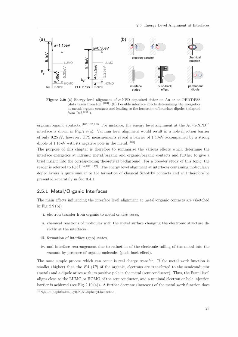
2.5 Energy Level Alignment at Interfaces
α
Δ
α
Δ
Figure 2.9: (a) Energy level alignment of α-NPD deposited either on Au or on PEDT:PSS(data taken from Ref. [104]) (b) Possible interface effects determining the energeticsat metal/organic contacts and leading to the formation of interface dipoles (adaptedfrom Ref. [105]).
organic/organic contacts. [105,107,108] For instance, the energy level alignment at the Au/α-NPD13
interface is shown in Fig. 2.9 (a). Vacuum level alignment would result in a hole injection barrierof only 0.25 eV, however, UPS measurements reveal a barrier of 1.40 eV accompanied by a strongdipole of 1.15 eV with its negative pole in the metal. [104]
The purpose of this chapter is therefore to summarize the various effects which determine theinterface energetics at intrinsic metal/organic and organic/organic contacts and further to give abrief insight into the corresponding theoretical background. For a broader study of this topic, thereader is referred to Ref. [105,107–112]. The energy level alignment at interfaces containing molecularlydoped layers is quite similar to the formation of classical Schottky contacts and will therefore bepresented separately in Sec. 3.4.1.
2.5.1 Metal/Organic Interfaces
The main effects influencing the interface level alignment at metal/organic contacts are (sketchedin Fig. 2.9 (b))
i. electron transfer from organic to metal or vise versa,
ii. chemical reactions of molecules with the metal surface changing the electronic structure di-rectly at the interfaces,
iii. formation of interface (gap) states,
iv. and interface rearrangement due to reduction of the electronic tailing of the metal into thevacuum by presence of organic molecules (push-back effect).
The most simple process which can occur is real charge transfer. If the metal work function issmaller (higher) than the EA (IP) of the organic, electrons are transferred to the semiconductor(metal) and a dipole arises with its positive pole in the metal (semiconductor). Thus, the Fermi levelaligns close to the LUMO or HOMO of the semiconductor, and a minimal electron or hole injectionbarrier is achieved (see Fig. 2.10 (a)). A further decrease (increase) of the metal work function does13N,N’-di(naphthalen-1-yl)-N,N’-diphenyl-benzidine
23

2 Fundamentals of Molecular Semiconductors
Δ ΔΔ Δ
Figure 2.10: (a) Illustration of Fermi level pinning at metal/organic interfaces upon chargetransfer, which occurs if either Wfmet < EA (a1) or IP < Wfmet (a2). Dependingon the value of Wfmet, different strong interface dipoles Δi appear. (b) MeasuredFermi level positions of various organic materials versus the applied substratework function (adapted from Ref. [113]). For each material, the Fermi level pinningregime is clearly verified (characterized by S = 0).
not reduce the barriers more, only the amount of transferred charges and hence the resulting dipoleincreases. Two different reasons are discussed in literature for this kind of Fermi level pinning.On the on hand, it has been argued that the Fermi level is pinned directly at the tailing states ofthe HOMO or LUMO DOS a few 100meV below the UPS/IPES-onset values. [108,114] Against that,Tengstedt et al. proposed that the pinning corresponds to the formation of an interfacial dipoleby means of charge transfer across the metal/organic interface in that amount which shifts thepolaronic level of the organic material to the position of the substrate Fermi level. [109,113] In otherwords, the Fermi level pins at the polaron levels which are formed at the interface upon an integercharge transfer (ICT model). Indeed, charge transfer across the metal/organic interface is expected,if the substrate work function is greater than the positive polaron/bipolaron formation energy forthe organic. [115,116] Here, it is important that the pinning energy is independent of the underlyingsubstrate type (metal, oxide, organic), i.e. independent of the respective screening properties. Thisis shown in Fig. 2.10 (b) where the Fermi level position with respect to the vacuum level for variousorganic semiconductors is plotted versus the applied substrate work function. For all materialsa clear substrate-independent pinning a few 100 meV above the respective IP values is confirmed.Furthermore, gap narrowing at the Ag/PTCDA14 interface due to polarization has been confirmedby combined UPS and IPES measurements. [117] Furthermore, occupied relaxed LUMO states in thegap at the Ag/PTCBI15 interface have directly been made visible, [107,110] strongly supporting thehypothesis of Fermi level pinning at polaron levels.In case of a metal work function lying within the semiconductor gap, i.e. EA < Wfmet < IP, nocharges are ideally transferred and vacuum level alignment is possible. Hence, a variation of the metalwork function Wfmet equally shifts the organic Fermi level Wforg, i.e. the respective electron or holeinjection barrier (cf. Fig. 2.11 (a1)), until EF pinning at the polaron states is reached as illustratedin Fig. 2.10 (a). However, for real metal/organic contacts, even for the case EA < Wfmet < IP,interface dipoles are often observed, e.g. 1.16 eV at the Ag(Wf = 4.39 eV)/MeO-TPD(IP = 5.07 eV)
143,4,9,10-perylentetracarbonsäuredianhydrid15perylene-tetracarboxylic-bis-benzimidazole
24

2.5 Energy Level Alignment at Interfaces
Δα
Figure 2.11: (a) Illustration of possible energy level alignments at metal/organic contacts ifEA < Wfmet < IP. Varying the substrate work function could lead to an equal(S = 1) or weaker (S < 1) shift of the interface Fermi level. In the latter casean interface dipole appears. (b) Collection of the level alignment characteristics(slope parameters S) of different organic materials deposited on various substrates(adapted from Ref. [107]).
interface. To describe the impact of a substrate work function variation dWfmet on the interfaceenergy level alignment to an organic material, i.e. on the interface Fermi level position, the slopeparameter S is commonly defined by
S ≡ dEF
dWfmet=
dWforgdWfsub
. (2.28)
Here, Wforg denotes the difference between the Fermi and the vacuum level. The two scenarios de-scribed above reflect special cases: As labeled in Fig. 2.10 (b), Fermi level pinning at polaron levelscorresponds to S = 0 (Bardeen Limit), whereas freely tunable injection barriers correspond to S = 1
(Schottky-Mott Limit). However, usually slope parameters in between 0 < S < 1 are experimentallyfound, [107] examples are given in Fig. 2.11 (b). Reasons for this behavior are the push-back effect,formation of interface states, and/or chemical reactions (cf. Fig. 2.9 (b)).Push-back effect in this context means lowering of the metal work function upon adsorption ofmolecules. [105] Actually, the work function of a metal Wfmet is the sum of bulk and surface contri-butions, namely the bulk chemical potential μ and the surface dipole. [118] The latter depends onthe tailing of the electronic wave function into the vacuum, and is hence sensitively influenced bypresence of molecules. Particularly, the repulsion between the electrons in the molecular orbitals ofthe organics and the metal lead to an effective reduction of Wfmet. In consequence, the hole injectionbarrier is typically increased in comparison to the simple assumption of vacuum level alignment andneglecting the push-back effect. For instance, this has been reported for 6P16 or α-NPD on Au. [104]
However, the push-back can be avoided by using polymer electrodes like PEDOT:PSS rather thanAu (cf. Fig. 2.9 (a)). Indeed, α-NPD, pentacene, and 6P deposited on PEDOT:PSS show hole injec-tion barriers lowered by up to 1 eV compared to Au although the work functions of both substratematerials are quite similar (Wf ≈ 5.1 eV). [104,107] The reason for this improvement is the muchlower contribution of the surface dipole to the work function in case of the polymer. Alternatively,surface treatment of metals can significantly weaken the push-back effect. Although the metal work
16para-sexiphenyl
25

2 Fundamentals of Molecular Semiconductors
function is strongly reduced by thin contamination layers compared to sputter cleaned surfaces, e.g.from 5.4 eV (clean) to 4.7 eV for contaminated Au, the hole injection barriers to 6T or α-NPD arenonetheless decreased by several 100 meV upon contamination. [112,119] Similar results were reportedfor Ag, Pt, and Pd contacts. [112] Here, it is important that the contamination layer does not elec-tronically decouple the two materials, i.e. that they are in direct thermodynamic equilibrium. [112]
Practically, this is realized by contamination thicknesses of less than 2 nm.Besides the push-back effect, the energy level alignment at metal/organic interfaces can be stronglyinfluenced by possible chemical reactions. The prototypical interface, which has been extensivelystudied by core level analysis by XPS, is the Mg/Alq3 contact. [107,120–122] Here, it has been foundthat a chemical reaction leads to the formation of interface gap states which cause Fermi level pin-ning.However, even by avoiding the push-back effect as well as chemical reactions, the slope parametercan be still smaller than 1 (for EA < Wfsub < IP), which has been attributed to the formation ofmetal-induced gap states (MIGS) in the organic semiconductor. [123,124] This theory of barrier for-mation is well established for classical metal/semiconductor contacts. [57,125,126] It has been arguedby Flores et al. that the energetic interface alignment is governed by [125]
i. the metal wave function tunneling into the semiconductor gap, changing there the surfacestates, and
ii. that the new gap DOS is compensated by a decrease in the conduction and/or valence bandDOS .
Furthermore, a charge neutrality level (CNL) can be defined such that total integrated density ofgap states up to the CNL accommodates the number of electrons from the conduction band. Hence,the charge transfer at a metal/semiconductor interface is controlled by the difference between themetal Fermi level and the semiconductor CNL determining the direction and amount of CT, whichfurther introduces a dipole, aligning the metal EF and the CNL. In 2004, Vazquez et al. suggestedto transfer the MIGS model to intrinsic metal/organic contacts, i.e. to assume that the interfaceFermi level is controlled by metal-induced gap states of sufficiently high density. In particular, theycalculated the CNL of PTCDA and the interface alignment of the Au(111)/PTCDA contact byDFT. [124] In this context, a slope parameter of S ≈ 0.13 has been suggested for this material. Ina more extended study, the interface properties of PTCDA, PTCBI, and CBP on Au(111) havebeen analyzed by the MIGS model and finally compared to UPS measurements, yielding deviations< 0.2 eV between theory and experiment for the interface Fermi level position EF and the slopeparameter S. [123] Here, the proposed neutrality condition for the interface alignment of EF is
CNL− EF = S · (CNL−Wfmet) . (2.29)
Furthermore, the slope parameter is specified by
S =dEF
dWfmet=
1
1 + 4πe2D(EF )δ/A, (2.30)
with D(EF ) being the density of induced states at the Fermi energy, δ the distance between thecharges induced in the metal and the organic molecule (Au(111)/PTCDA: 2.8 . . . 3.2Å), and A the
26

2.5 Energy Level Alignment at Interfaces
area associated with one molecule (PTCDA: 120Å2).Finally, Vazquez et al. stated that the charge neutrality level seems to be an intrinsic property of anorganic material since they found a very weak sensitivity of the CNL on the chosen metal/organicinterface in their calculations. [124] This conclusion is important for the further theoretical explana-tion of the level alignment at organic/organic contacts, which will be briefly summarized in the nextsection.
2.5.2 Organic/Organic Interfaces
Due to weak Van-der-Waals interactions between organic molecules, vacuum level alignment is typi-cally observed at organic/organic contacts. [110,127–130] A review on various organic/organic contactsinvestigated by UPS has been published by Hill et al. already in 2000. [110] Although in the mostcases vacuum level alignment could be identified, there are exceptions which show strong inter-face dipoles, e.g. 0.5 eV at the PTCDA/ALq3, [110] 0.6 eV at the TTF/TCNQ, [131] or 0.25 eV at theZnPc/ZnPc:C60(1:1) interface. [132] In particular, if the energetic gaps of both materials involved donot overlap, charge transfer occurs and a dipole arises, for instance, 1.1 eV at the CuPc/F16CuPcinterface due to complete electron transfer from CuPc (IP = 4.8 eV) to F16CuPc (EA = 5.2 eV). [133]
Since the energy level alignment of metal/organic contacts is determined by the formation of metal-induced gap states depending on the metal (if S > 0), the alignment of a respective overlyingorganic/organic contact can differ for various metal substrates underneath, e.g. this has been re-ported for Alq3/CuPc evaporated either on ITO or on Mg. [134]
In 2005, Vazquez et al. suggested the adoption of the concept of the charge neutrality level CNL (cf.Sec. 2.5.1) to organic/organic interfaces. [135] In particular, it has been stated that the position ofthe CNL is an intrinsic property of an organic material independent of the contact material, whichmakes it reasonable to treat it as an effective Fermi level. Consequently, the relative distance of theCNLs of two organic materials before contact determines the direction of charge transfer and hencedefines the strength and direction of an appearing dipole. The suggested neutrality condition reads
Δ = (1− S)(CNL1 − CNL2)inital . (2.31)
Here, S is a screening parameter determined by the dielectric constants εi of the organic materialsand defined by
S =1
2
(1
ε1+
1
ε2
). (2.32)
For verification of this approach, Vazquez et al. calculated the interface dipoles between variousorganic/organic contacts in comparison to UPS measurements, e.g. yielding Δtheory = 0.43 eV vs.ΔUPS = 0.4 eV for the PTCDA/CuPc interface. However, in the most cases, dipoles smaller than0.1 eV are obtained by the model, which agrees with the common observation of vacuum levelalignment at these interfaces by UPS.
27

2 Fundamentals of Molecular Semiconductors
28

3 | Molecular Doping
The fundamentals of molecular doping will be presented in this chapter. First, abrief introduction covers the main aspects and definitions of molecular doping. Inthe second section, a summary about various dopant compounds, historically andnowadays applied in the field of organic electronics, is given. Afterwards, the currentunderstanding of the molecular doping mechanism is discussed. Finally, the basics oforganic Schottky contacts as well as p-i-n diodes as tools to study organic doping aresummarized.
3.1 Introduction to Molecular Doping: Terms and Definitions
Molecular doping is also referred to as electrical, conductivity, or redox doping in literature. Itdescribes the admixture of dopant molecules to a host material in order to increase significantly itsconductivity
σ = e ·μ · p . (3.1)
Here, p is the density of free charge carriers and μ the effective carrier mobility. For real conductivitydoping, a charge transfer from dopant to host molecules is necessary, which increases the absolutenumber of free charge carriers p. This process requires well matched energy levels as sketchedin Fig. 3.1. In case of p-doping (n-doping), the LUMO (HOMO) of the dopant molecules hasideally to lie energetically below (above) the HOMO (LUMO) of the host material. Empirically, thecorresponding energy levels have to be aligned such that the dopant LUMO (HOMO) lies at most0.5 eV (above) below the host HOMO (LUMO). [136] Otherwise, the energy barrier is too high toallow for sufficient charge transfer. The whole doping process can be described by a two-step model.Considering for instance p-doping of a matrix material M , in a first step, electrons are transferredto p-dopant molecules A, and charge transfer complexes [M+A−] are formed. These complexes arefurther dissociated into ionized dopants A− and free holes M+.Besides the generation of free charge carriers p, molecular doping also increases the mobility μ dueto filling of deep trap and shallow tail states. Hence, the conductivity σ is usually a complicated andnot easily predictable function of the doping concentration (details discussed in Sec. 3.3). However,the most important effect of doping for the application in functional devices is the reduction ofdepletion layers thicknesses at metal/organic contacts, which provides ohmic injection propertiesindependent of the contact material. [13]
The term molecular doping is also used to describe the mixing of two materials with the aim toincrease the mobility without the generation of free charges. For instance, this has been shown
29

3 Molecular Doping
Figure 3.1: Principle of molecular doping: If the energy levels are well aligned, n-type (p-type)doping is provided by electron transfer from the HOMO of a dopant (host) to theLUMO of a host (dopant) molecule.
for doping 2wt% PBD1 as “n-dopant” into BCP2. [137] Additionally, there is also the term “chemicaldoping”, [138] which means the formation of a high mobility compound by blending two initial organicmaterials, e.g. mixing PDOT3 with PSS4. [139]
Finally, the physical quantities and units representing the doping concentration are presented here.The molar doping ratio MR is defined as the ratio of the density of dopant molecules nd per hostmolecules nh, whereas the doping concentration cn gives the number of dopant molecules per totalnumber of molecules, i.e. per dopants and hosts:
MR =nd
nh; cn[mol%] = 100% · nd
nd + nh; cn = 100% · MR
MR + 1. (3.2)
Additionally, it is common to use similar quantities relating to the deposited weight of the matrix anddopant materials because they can directly be measured by quartz crystal micro-balances (QCMs)during film deposition. Here, the weight ratio WR is defined as the deposited mass of dopants md
per mass of host material mh. The respective mass doping concentration cm is hence given by themass of dopant material per total film mass:
WR =md
mh; cm[wt%] = 100% · md
md +mh; cm = 100% · WR
WR + 1. (3.3)
The mass and number density quantities are correlated by the corresponding molar masses Mi ofboth materials by mi = Mi ·ni ·V , which finally gives the conversion
WR = MR · Md
Mh. (3.4)
12-(4-biphenyl)-5-(4-tert-butylphenyl)-1,3,4-oxadiazole22,9-Dimethyl-4,7-diphenyl-1,10-phenanthroline3poly-3,4-ethylenedioxythiophene4polystyrene sulfonate
30

3.2 Historical Development of Dopant Compounds
Typical doping concentrations cm applied in the field of organic electronics are in the range of a fewweight percent (wt%), [13,14] i.e. much higher than in classical single-crystal semiconductors. [57] How-ever, it is necessary to extend the range of doping concentrations below MR = 10−3 for fundamentalstudies on the molecular doping mechanism. [140,141]
3.2 Historical Development of Dopant Compounds
3.2.1 Early Doping Work with Metals and Gases
In analogy to inorganic semiconductors, elemental materials (metals, ions), or gases (e.g. iodine,bromine) are used in first studies on doping organic semiconductors. However, the main problemsof these approaches are high required doping ratios as well as the limited stability, [142] e.g. de-doping effects (removal of dopants) after stopping the exposure of the organics to gases. In earlyworks, p-doping of phthalocyanines by ortho-chloranil, [143] TCNQ5, [144] and DDQ6 [145–147] is stud-ied. Additionally, already in the 1990’s organic rectification diodes have been realized by dopedlayers. [148,149]
More recently, metal-oxides as WoOx, [150,151] ReOx, [152,153] or MoOx[154] have been used as hole in-
jection layers [155–157] or p-dopants. [154,158–162] Even p-doping of the fullerene C60 by MoOx has beenreported, [163] which is difficult considering the low HOMO level of C60. However, these materialspossess high evaporation temperatures, and are technically difficult to control during co-evaporation,in particular at lower rates.Molecular n-type doping is more challenging than p-doping, because compounds with work func-tions < 3.5 eV are needed to dope typical OLED transport materials. [13] Typical electron donatingmaterials are alkali metals. [164] In particular, n-doping with lithium, [165] (e.g. in form of Li quino-line or LiO2) or using LiF as electron injection layer, [166–168] as well as doping with Cs, [169,170]
CsF, [138,171] Cs2CO3, [153,172], Cs3PO4, [173] or CsN3[174] has been shown. LiF dissociation upon
subsequent hot metal deposition (cathode) followed by Li diffusion into the adjacent ETL material,leading to an n-doping effect, has been proposed as working mechanism. [175] However, the ten-dency of these materials to diffuse through functional devices is problematic, as it can cause excitonquenching in emission layers of OLEDs and reduces the lifetime. [176,177] Furthermore, the formationof well-defined doping profiles is prevented by the high diffusivity of the small metal atoms, nega-tively impacting the device stability. Additionally, the high doping concentrations required to reachdesired conductivities disturb the transport of free electrons by the formation of trap states due toCoulomb attraction of the high number of ionized counter-ions.Due to these drawbacks of doping with metals and gases, organic molecules as conductivity dopantshave been developed, which will be outlined in the next section.
3.2.2 Organic Molecules as Conductivity Dopants
Due to their higher mass, molecules tend to diffuse through organic devices much less than puremetals, wherefore the research focused on the development of molecular dopants over the last two
57,7’,8,8’-tetracyanoquinodimethane6dichlorodicyanoquinone
31

3 Molecular Doping
decades. The first prominent p-dopant is F4-TCNQ7 (IP = 8.34 eV, EA = 5.24 eV), [10,178] which wassuccessfully doped into phthalocyanines, [10,178–180] m-MTDATA8, [181] α-NPD9, [182,183] and MeO-TPD10. [184] Furthermore, it was used to significantly reduce the operation voltage of small moleculeOLEDs, [185] employing the so-called p-i-n concept. [13] However, the main disadvantage of this p-dopant is its low vapor pressure and thus its tendency to contamination of vacuum chambers.Therefore, alternative (similar) molecular p-dopants have been synthesized within the last years,namely F2-HCNQ11, [186] or F6-TCNNQ12. [187] Another promising new p-dopant of high molecularmass is the fluorinated fullerene C60F36, [188] which can easily p-dope the standard OLED HTLmaterial MeO-TPD. [189,190]
As already mentioned, the development of efficient n-type dopants is much more challenging thanp-dopants, because very high lying HOMO levels are required to donate electrons to the LUMO ofOLED ETL materials, which are typically in the range of 3 eV. [13] Hence, molecular n-dopants areeasily oxidized in air and have to be handled under inert atmosphere. Early investigations on molec-ular n-type doping comprise the work of Nollau et al., in which NTCDA13 has been doped by BEDT-TTF14. [191] Later, TTN15 was presented as a donor material which can n-dope F16ZnPc. [192] Addi-tionally, the Kahn group published various n-doping studies, using CoCp2
16 doped into NTCDA, [193]
THAP17, [194] or pentacene, [195] as well as DMC18 doped into CuPc. [196] Another class of very effi-cient n-dopants, which possesses extremely low IPs of less than 3 eV, [197] are the di-metal-organiccomplexes W2(hpp)4 and Cr2(hpp)4. [198–200] Doping these molecules into C60 thin-films leads tovery high conductivities of up to 4 S/cm. [201]
3.2.3 Precursor Molecules
Using so-called "precursor" molecules as conductivity dopants is a sophisticated way to circumventthe disadvantages of alkali metals (cf. Sec. 3.2.1) and non air-stable molecular n-type dopants (cf.Sec. 3.2.2). This approach to conductivity doping is based on the in situ activation of the donorfrom a stable precursor compound by light or thermal energy during or after the co-evaporation ofdopant and matrix materials. In the mixed film, electron transfer to the matrix occurs accompaniedby the formation of donor cations.This concept was introduced by Werner et al. in 2003, [202] where successful n-doping of NTCDAfilms by pyronine B (PyB) chloride has been demonstrated, where leuco pyronine B is formedduring evaporation being the actual n-dopant. [202,203] Later, UPS measurements on NTCDA:PyBfilms indicate the presence of both, the leuco and the neutral radical forms of PyB in condensedfilms. [204] The resulting doping mechanism is thus given by the generation of reducing radicals D•
from thermal deposition of salts of stable cations D+Cl−, which can be summarized by the reaction
72,3,5,6-tetrafluoro-7,7,8,8-tetracyanoquinodimethane84,4’,4”-tris(3-methyl-phenyl-phenyl-amino)triphenylamine9N,N’-Di(naphthalen-1-yl)-N,N’-diphenyl-benzidine
10N,N,N’,N’-Tetrakis(4-methoxyphenyl)-benzidine113,6-difluoro-2,5,7,7,8,8-hexacyanoquinodimethane122,2’-(perfluoronaphthalene-2,6-diylidene)dimalononitrile13Naphthalenetetracarboxylic dianhydride14bis(ethylenedithio)-tetrathiafulvalene15tetrathianaphthacene16bis(cyclopentadienyl)-cobalt(II) cobaltocene17tris(thieno)hexaazatriphenylene18decamethylcobaltocene
32
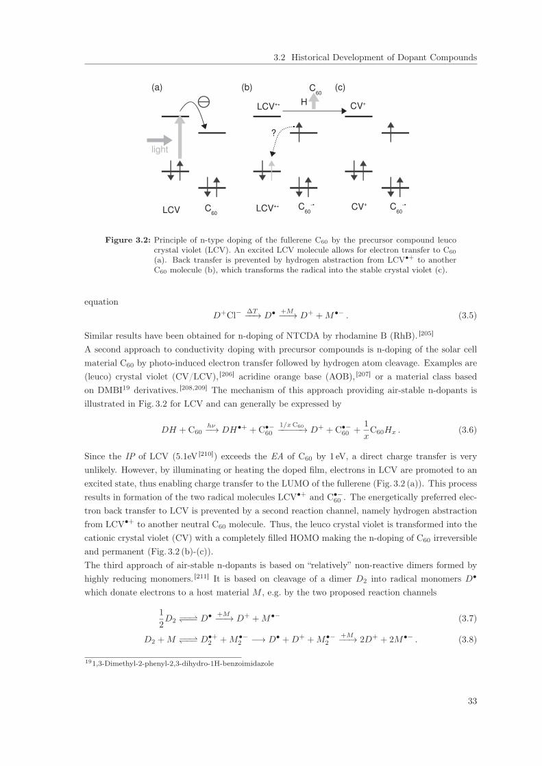
3.2 Historical Development of Dopant Compounds
LCV C
60C
60-.LCV+.
?
C60
-.CV+
LCV+. CV+
C60
H
(a) (b) (c)
light
Figure 3.2: Principle of n-type doping of the fullerene C60 by the precursor compound leucocrystal violet (LCV). An excited LCV molecule allows for electron transfer to C60
(a). Back transfer is prevented by hydrogen abstraction from LCV•+ to anotherC60 molecule (b), which transforms the radical into the stable crystal violet (c).
equationD+Cl− ΔT−−→ D• +M−−→ D+ +M•− . (3.5)
Similar results have been obtained for n-doping of NTCDA by rhodamine B (RhB). [205]
A second approach to conductivity doping with precursor compounds is n-doping of the solar cellmaterial C60 by photo-induced electron transfer followed by hydrogen atom cleavage. Examples are(leuco) crystal violet (CV/LCV), [206] acridine orange base (AOB), [207] or a material class basedon DMBI19 derivatives. [208,209] The mechanism of this approach providing air-stable n-dopants isillustrated in Fig. 3.2 for LCV and can generally be expressed by
DH +C60hν−→ DH•+ +C•−60
1/xC60−−−−−→ D+ +C•−60 +1
xC60Hx . (3.6)
Since the IP of LCV (5.1eV [210]) exceeds the EA of C60 by 1 eV, a direct charge transfer is veryunlikely. However, by illuminating or heating the doped film, electrons in LCV are promoted to anexcited state, thus enabling charge transfer to the LUMO of the fullerene (Fig. 3.2 (a)). This processresults in formation of the two radical molecules LCV•+ and C•−60 . The energetically preferred elec-tron back transfer to LCV is prevented by a second reaction channel, namely hydrogen abstractionfrom LCV•+ to another neutral C60 molecule. Thus, the leuco crystal violet is transformed into thecationic crystal violet (CV) with a completely filled HOMO making the n-doping of C60 irreversibleand permanent (Fig. 3.2 (b)-(c)).The third approach of air-stable n-dopants is based on “relatively” non-reactive dimers formed byhighly reducing monomers. [211] It is based on cleavage of a dimer D2 into radical monomers D•
which donate electrons to a host material M , e.g. by the two proposed reaction channels
1
2D2
+M−−⇀↽−− D• +M−−→ D+ +M•− (3.7)
D2 +M+M−−⇀↽−− D•+2 +M•−
2 −→ D• +D+ +M•−2
+M−−→ 2D+ + 2M•− . (3.8)
191,3-Dimethyl-2-phenyl-2,3-dihydro-1H-benzoimidazole
33
3 Molecular Doping
For instance, successful doping of CuPc [211] and C60[140,212] by [RuCp*(mes)]220 has been demon-
strated. Originally, this approach of n-doping by precursor molecules has already been proposed bya patent application of Limmert at al. in 2006. [213]
3.2.4 Electrical Doping of Polymers
Electrical doping of polymers is ambiguous. On the one hand, chemical doping can occur, i.e. theinitial polymer is chemically modified by adding “dopant“ molecules, positively affecting its mobility.On the other hand, real p- or n-type doping of polymeric films was achieved, i.e. the number of freecharge carriers is significantly increased upon admixture with dopant compounds.However, first works focused on the introduction of polymeric injection layers to improve device effi-ciencies, e.g. of P3MT21 layer as anode contact material in perylene OLEDs, [214] or of polyaniline inMEH-PPV22 OLEDs. [215] Later, chemical doping of polymers with inorganic salts has been demon-strated, e.g. polythiophene doped by FeCl3, [216] or a spin-coated TPD form doped by SbCl5. [217]
Further examples are iodine doped MEH-PPV, [218] and polycarbonate doped with a chloroanti-monate (TBAHA). [219,220] However, the most prominent example for chemical doping is the for-mation of PDOT:PSS. [139] Analysis of the chemical processes providing the doping effect revealthat PDOT:PSS forms a degenerated semiconductor, i.e. metallic complexes which are surroundedby isolating PSS. [221,222] The electrical transport occurs via hopping or percolation between themetallic polymer chains. Nevertheless, in contrast to really molecularly doped films which showan Arrhenius-like temperature dependence of the conductivity, [179] PDOT:PSS films exhibit a pro-portionality of log(σ) to 1/T 1/2. [223] As a nice side effect, chemically doped polymers are typicallytransparent in contrast to their initial educts, making them favorable as contact materials in trans-parent OLEDs or OPV. This is due to the fact that neutral polymer chains become charged, whichblue shifts their absorption into the near UV region. [136]
Besides chemical doping, in more recent works actual conductivity doping has been shown for (spin-coated) polymers. In 2007, Aziz et al. showed molecular p-doping of the polythiophene P3HT23
by F4-TCNQ dissolved in chloroform. P-doping with F4-TCNQ from solution via mixing dopantsolutions to host solutions has further been published for PFB24, TFB25 and F8BT26, [224] as wellas for MEH-PPV, [225] revealing generally similar conductivity, FTIR, and absorption changes aspreviously observed for small molecule based systems. [13] Most recently, Pingel et al. found for thesystem P3HT:F4-TCNQ that the CT amount is rather high as ≈ 70%, whereas only 5% of thedopants actually provide free carriers. [226] Furthermore, the mobility of these doped films seems tobe a complicated function of the doping concentration. [227]
However, some properties of molecular doped films seem to be universal, i.e. independent of theprocessing conditions and molecule sizes (polymers vs. small molecules), which motivated severalattempts towards a generalized theory describing the underlying physics of molecular doping. Thesetheories are presented in the next section.
20ruthenium(pentamethylcyclopentadienyl)(1,3,5,-tri-methylbenzene) dimer21poly(3-methylthiophene22poly[2-methoxy,5-(2’-ethyl-hexyloxyl)-1,4-phenylene vinylene]23poly(3-hexylthiophene)24poly(9,9-di-n-octylfluorene-alt-bis-N,N-(4-butylphenyl)-bis-N,N-phenyl-1,4-phenylenediamine)25poly(9,9-di-n-octylfluorene-alt-(1,4-phenylene-((4-sec-butylphenyl)imino)-1,4-phenylene))26poly(9,9-di-n-octylfluorene-alt-benzothiadiazole)
34

3.3 Prevailing Theories on the Molecular Doping Process
3.3 Prevailing Theories on the Molecular Doping Process
Molecular doping aims a significant increase of the conductivity of charge transport layers in func-tional organic devices in order to minimize ohmic losses. Since not only the carrier density p, butalso the effective mobility μ of the organic semiconductor is influenced by doping, a comprehensivetheoretical description of the molecular doping process must be closely related to the transportphenomena in the respective organic material. As presented in Sec. 2.3, charge carrier transportprocesses in organic semiconductors strongly depend on their thin-film morphologies and on thetemperature regime, i.e. band, band-like, hopping or percolation transport. Hence, a general theoryunifying molecular doping and transport process in organic materials cannot be expected. However,different models describing the molecular doping process have been developed over the last decadein order to explain experimental conductivity data of specific material combinations. In particular,measured doping efficiencies ηdop, defined as the ratio of free charge carriers p provided by dopingto the number of dopant molecules NA
ηdop =p
NA, (3.9)
have been compared to theoretical models. The experimental values vary for different material sys-tems (cf. Tab. 3.1), and often cannot be explained consistently. It is the purpose of this section tosummarize and compare prevailing theories on the molecular doping process, and thus provide thetheoretical background for ranking the results obtained in the framework of this PhD thesis.
Considerations based on the Law of Mass Action. The standard model describes moleculardoping as a two-step process. [205,228] First, an electron or hole is transferred from a dopant to ahost molecule if the energy levels are well aligned (cf. Fig. 3.1), forming a CT complex [M+A−]. Forgeneration of free charges, which can move through the host, this complex has to be dissociated ina second step. The whole process hence reads, e.g. for p-doping of a host material M by acceptormolecules A:
MMAM︸ ︷︷ ︸neutral
iK1i⇐=⇒M [M+A−]M︸ ︷︷ ︸CT state
iK2i⇐=⇒MM+A−M +M⇐=⇒M+MA−M︸ ︷︷ ︸free charge carrier
. (3.10)
The generation efficiency of free charge carriers can hence be estimated by the law of mass actionto
K =NM+NA−
NMNA= exp
(− ΔE
kBT
). (3.11)
Here, Ni are the number densities of species i, and the reaction constant K determines whether theequilibrium lies more on the left or on the right side of Eq. (3.10). Since the doping process consistsof two steps, the reaction constant can be split up into K = K1 ·K2 defining the sub-steps. In mostcases, the overall doping efficiency ηdop is actually low, although the probability of integer chargetransfer is close to unity. [13] In other words, the equilibrium of reaction K1 lies on the right side andof K2 on the left side. The reason for this imbalance is the comparably high binding energy ΔEB
35

3 Molecular Doping
of the CT state which has to be overcome for liberation of a free charge carrier:
K2 =NM+NA−
NMN[M+A−]= exp
(−ΔEB
kBT
). (3.12)
The CT state binding energy can be estimated by a simple Coulomb approach to [25]
EB(r) =1
4πε0
e2
r+ Pe−h(r)− (Pe + Ph) � 1
4πε0εr
e2
r, (3.13)
with the energy Pe−h gained by the CT state upon polarization of its surrounding molecules, andsimilar energies Pe and Ph for the separated electron and hole. Alternatively, EB(r) can be ex-pressed by introduction of an effective dielectric constant εr of the organic material. Assuming atypical experimental value of εr ≈ 3, [95] and an intermolecular distance of r � 1 nm yields a CTstate binding energy of EB � 0.5 eV. Hence, only a small fraction of all CT states is expected tobe dissociated at room temperature (kBT = 0.025 eV) by assuming thermal Boltzmann activationexp (−ΔEB/kBT ) in Eq. (3.12). However, it has to kept in mind that the electron additionallygained an energy equal to the difference IPhost − EAdopant during step K1, which might furthersupport the CT dissociation. Therefore, it is reasonable to introduce an effective activation energyΔE for the whole doping process K, which is actually lower than ΔEB , and defines the equilibriumstate of Eq. (3.11). This conclusion suggests to describe the whole doping process not by this two-step model, but by a two-level system similar to classical semiconductor physics. In this context,the question arises whether deep or shallow states are the more appropriate model. [205,228] This isdiscussed exemplarily for p-doping in the following.
Deep and Shallow Acceptor States. In classical semiconductor physics, doping is describedby thermal activation of charge carriers from (single) dopant levels located in the gap to the edgesof the conduction or valence band. [57] In this effective two-level system, the equilibrium is definedby Fermi-Dirac statistics:
f(E,EF ) =1
1 + exp(
E−EF
kBT
) . (3.14)
Here, f(E,EF ) gives the occupation probability of a state at energy E with electrons for a givenposition of the Fermi level EF (electro-chemical potential). Hence, the occupation of a single acceptorlevel EA with electrons, which is the case for p-doping, is given by
N−A =
NA
1 + exp(
EA−EF
kBT
) . (3.15)
Here, N−A is the number density of negatively charged acceptor states EA and NA the density of
all acceptor states. However, the assumption of single levels reflect more an idealized condition,in real semiconductors the energy levels are broadened or complicated distributions of states arepresent. [57] The number of occupied states for any distribution of states is given by a respectiveFermi-integral, e.g. the number of holes within the density of valence states gV (E) reads
p =
∫ +∞
−∞dE gV (E)[1− f(E,EF )] . (3.16)
36

3.3 Prevailing Theories on the Molecular Doping Process
The term [1−f(E,EF )] appears because free holes correspond to states not occupied with electrons.For classical semiconductors, the density of valence states is assumed to be parabolic, [57] i.e. gV (E) ∝√E − EV , in which EV is the valence band edge. Solving the corresponding Fermi-integral under
the assumption of Boltzmann approximation yields the well known expression
p = NV exp
(EV − EF
kBT
). (3.17)
Here, NV is the effective density at the valence band edge EV . For p-doping, equilibrium betweenthe two levels EV and EA is determined by the relative position of the Fermi level, which is definedby the neutrality condition
p = N−A . (3.18)
As consequence, increasing the amount of acceptors NA and hence of free charge carriers p shiftsthe Fermi level closer to the band edge EV .If an acceptor level EA is treated as shallow or deep state actually depends on the temperature.Here, a state is considered as shallow impurity level if the Fermi level lies well above EA for alldoping concentrations NA, i.e. in any case all dopants are ionized independent of the temperature(cf. Fig. 3.3 (a)):
p = N−A = NA . (3.19)
This means that the number of free charge carriers increases linearly with the doping concentration.Furthermore, it follows from Eq. (3.17) that the Fermi level shifts linearly by a slope of kBT withthe logarithm of the doping concentration towards the band edge EV :
EF = EV − kBT lnNA
NV. (3.20)
In case of a deep dopant level, the Fermi level lies below EA and the dopants are only partiallyoccupied with electrons depending on the temperature (cf. Fig. 3.3 (a)). The thermal activationenergy is given by
ΔEp,act =EA − EV
2(3.21)
and the number of free charge carriers can be estimated by combining Eq. (3.17) and Eq. (3.15) to
p(T ) �√NANV exp
(−ΔEp,act
kBT
). (3.22)
The shift of the Fermi level with the logarithm of the doping concentration is now reduced by afactor of two:
EF (T ) =EA + EV
2− kBT
2lnNA
NV. (3.23)
This result is reasonable because the acceptor level acts now as a kind of impurity level which pinsthe Fermi level close to its energetic position, i.e. it prevents a shift of EF closer than (EA−EV )/2
to EV . However, the number of free charge carriers at the valence edge is equal for a fixed positionof the Fermi level regardless of a shallow or deep acceptor level (cf. Fig. 3.3 (a)). The differencebetween these two limiting cases lies in the absolute numbers of impurities NA which are necessaryto shift EF to this certain position.
37

3 Molecular Doping
Figure 3.3: (a) Schematic energy level diagram for a p-doped semiconductor with either ashallow or a deep acceptor state EA. (b) Corresponding log(p) vs. 1/T plot,characterizing the dopant reserve, saturation and intrinsic temperature regime at afixed doping concentration NA.
At a fixed doping concentration NA, an impurity level EA can act as a shallow as well as a deepdopant state, depending on the actual temperature T . The corresponding number of free chargecarriers is schematically plotted in Fig. 3.3 (b) versus 1/T . At low temperatures, only a few dopantsare thermally activated, which is called freeze-out or impurity reserve regime and corresponds to adeep dopant level (N−
A < NA). Increasing T leads to an enhanced dopant activation until all presentacceptors are active. This regime is called dopant saturation and corresponds now to a shallowimpurity level (p = N−
A = NA). At very high temperatures, the intrinsic carrier concentration pi,determined by the law of mass action
p2i = NCNV exp
(EC − EV
kBT
), (3.24)
exceeds the density of carriers provided by doping. Here, EC and NC are the energy edge andthe effective density of the conduction band. On the other hand, a transition between impuritysaturation and reserve regimes can also occur at a fixed temperature by a very strong increase ofthe dopant density NA. In this case, the Fermi level crosses the dopant level EA and the dopingefficiency ηdop = p/NA drops below unity.Finally, it is discussed whether shallow or deep dopant states can be expected for molecular dopingat room temperature. The transition between both regimes is defined by EF = EA. If we assumestill dopant saturation at a very high doping concentration, e.g. at NA = NV /100, the maximumdifference EV −EA can be estimated by Eq. (3.17) to 120meV. Dopant saturation at a concentrationof even 10% requires a depth of only 60meV. However, as previously shown, CT state binding ener-gies in the range of 500meV or even 1 eV are calculated for PTCDA or pentacene [229] and thereforeexpected for molecular dopant:host systems in general. Hence, the formation of shallow dopantstates at room temperature is very unlikely by this argumentation and deep impurity levels seemthe more suitable model.
Comparison to Experiments: Contradictions and Challenges. The effect of moleculardoping has been intensively studied by conductivity, Seebeck, UPS, and IR-spectroscopy measure-ments, of which the most important results are summarized in this section. As already mentioned,
38

3.3 Prevailing Theories on the Molecular Doping Process
Figure 3.4: (a) Conductivity versus the molar doping ratio of MeO-TPD thin-films p-dopedby F4-TCNQ. (data taken from Ref. [11]) (b) Measured Seebeck coefficients S anddeduced charge carrier densities p versus the molar doping ratio of ZnPc thin-filmsp-doped by F4-TCNQ. (data taken from Ref. [180])
molecular doping increases the thin-film conductivity
σ(T,NA) = e · p(T,NA) ·μ(T, p) (3.25)
by orders of magnitude from an intrinsic level of σ < 10−10 S/cm to typical values of 10−5 . . . 1 S/cm
at doping levels of a few molar percent. Here, a super-linear increase of σ with the doping concen-tration is usually observed. [179,180] For instance, the conductivity of MeO-TPD thin-films doped byF4-TCNQ increases over-proportional with a slope of 1.85 by varying the molar doping ratio by twoorders of magnitude (cf. Fig. 3.4 (a)). [11] Furthermore, linear [230] and even sub-linear [231] behaviors,as well as transitions between the different regimes [140,180] were found. However, without any precisemeasurement of the dependency of the mobility on the doping concentration or directly the numberof free charge carriers p provided by doping, an unambiguous classification to shallow or deep dopantstates is not possible. Hence, thermo-electric measurements were performed in order to resolve theshift of the Fermi level as well as to directly estimate the carrier density p. The Seebeck coefficient27
is a direct measure for the distance between an average transport state Eμ and the Fermi level
S(T ) =kBe
(Eμ(T )− EF (T )
kBT+Aμ
), (3.26)
and therefore decreases with increasing doping concentration. [179,180] The scattering constant Aμ
reflects the actual type of transport and becomes zero for considering carrier transport via a dis-crete level Eμ. Thus, the charge carrier density can be estimated by comparison of Eq. (3.26) and
27Further details are given in Ref. [231].
39

3 Molecular Doping
Eq. (3.17) to
p = Nμexp
(−EF − Eμ
kBT
)� Nμexp
(− e
kBS(T )
). (3.27)
In Fig. 3.4 (b) measured Seebeck coefficients S and derived density of magnitude p of ZnPc filmsp-doped by F4-TCNQ are shown. [180] Varying the molar doping ratio by approximatley one orderyields a decrease of S by a factor of two and an increase in p by two orders, i.e. strongly super-linear. These experimental results suggest that for molecular host:dopant systems the conclusionthat doping forms deep states, which would posses a p ∝ √NA behavior, is wrong. This conclusion issupported by the fact that the measured Seebeck coefficients are nearly temperature independent, asshown for the MR = 0.01 sample in the inset of Fig. 3.4 (b). Similar results have been obtained alsofor other material systems. [179,207] However, the material system VOPc:F4-TCNQ shows a slightlytemperature dependent carrier density p, having a thermal activation energy of Eact,p ≈ 100meV
and hence an acceptor depth in the range of 0.2 eV. [179] This finding is not consistent with the factthat the Fermi level has to lie between EA and Eμ in case of a deep dopant state since the respectiveEF −Eμ differences obtained by Seebeck measurements are reduced to only 0.3 eV. [179] Furthermore,the thermal activation energy of the carrier density Eact,p often decreases with increasing dopingconcentration, [179,191,201,230] for which no convincing explanation could be given in framework ofthese Seebeck studies.The assumption of shallow states would mean p ∝ NA and a temperature independent carrierdensity p, which is as well in contradiction to the above experiments. A possible explanation forthe super-linear increase of the conductivity could be an electron conduction via dopant moleculesin particular at higher doping concentrations, which is however in disagreement with monotonouslydecreasing Seebeck coefficients. As solution of all theses discrepancies, an explanation based onthe assumption of shallow dopant states accompanied by a temperature dependent filling of trapstates was proposed. [179] Furthermore, an increase of the mobility with the doping concentrationdue to filling of tail states was discussed. [140,228] Here, the different slopes in various materials canbe explained by different filling of the respective density of states and the resulting impact on themobility. [232,233]
Another explanation for the super-linear increase of the conductivity is a doping concentrationdependent activation energy, i.e. acceptor level position EA. [234–236] Different mechanisms havebeen proposed that show a decrease of EA with increasing dopant density in the form of [234]
EA = EA,max − βN1/3A , (3.28)
where β is a fitting constant in the order of e2/4πε0εr. [236] The dominating reason for this relationis an increased effective dielectric constant εr since the high number of charges (provided by doping)in localized states improves the polarizability of the organic thin-film. In framework of the two-stepmodel described above, this means an improved dissociation probability at high doping concentra-tions due to a reduced CT state binding energy EB(r). Assuming further Boltzmann activation ofthe dopants, i.e. p = NAexp(−EA/kBT ), finally leads to
σ = e ·μ ·NAexp
(− EA
kBT
)= e ·μ ·NAexp
(−EA,max − βN
1/3A
kBT
). (3.29)
40

3.3 Prevailing Theories on the Molecular Doping Process
With this ansatz, measured (super-linear) conductivities of n-doped PPEED28 films could be fittedby applying EA,max = 0.23 eV and β = 6.5 · 10−8 eV cm. [234]
Similar to the variable activation energy EA concept, a concentration dependent ionization proba-bility of molecular dopants has been proposed to cause the observed super-linear conductivities. [16]
Mityashin et al. calculated the electrostatic interactions between F4-TCNQ molecules doped intoa three-dimensional pentacene crystal and its surroundings on a microscopic scale in order to de-termine the overall charge carrier generation efficiency at a given doping concentration. [16] Theyconcluded that charge carriers are only able to overcome the Coulomb dissociation barrier (steptwo) if sufficient strong pathways are generated by electrostatic disorder introduced by neighboringdopant molecules. Consequently, the charge carrier generation efficiency is supposed to be approxi-mately zero at very low concentrations (below 1%) and increases with rising doping concentration.However, conductivity measurements on the same material system reveal values about 10−2 S/cm
even at a molar doping ratio of only MR = 0.005, [231] which is in clear contradiction to the predic-tions of this model.
host:dopantcn ηdop Ref.
(mol%) (%)
MeO-TPD:F4-TCNNQ3.1 3.3
Ref. [11]6.1 4.217 3.9
Ir(piq)3:NDP2
0.5 63
Ref. [237]1.0 952.0 854.0 64
CBP:MoOx
2 0.5 Ref. [154]
1.9 1.9 Ref. [158]
P5:F4-TCNNQ0.3 ≈ 0
Ref. [16]1.0 65.0 23
P5:C60F36 0.1 64 Ref. [238]
Figure 3.5: Fermi level position of p-doped MeO-TPD with respect to theHOMO-onset (E = 0) determined by UPSversus the molar doping ratio (data takenfrom Ref. [11]).
Table 3.1: Overview about publisheddoping efficiencies ηdop = p/NA of var-ious material systems investigated bymeans of UPS, [11,154,158] impedance spec-troscopy, [237,238] or calculated. [16]
As seen above, the model of deep dopant states is not compatible with Seebeck studies for variousmaterial systems. However, also the assumption of classical shallow states cannot completely ex-plain the experimental findings. In particular, doping efficiencies ηdop measured by UPS are in the28liquid crystal perylene diimide (solid at room temperature)
41

3 Molecular Doping
range of only a few or a few tens percent rather than close to unity (cf. Tab. 3.1). On the otherhand, it seems that doping efficiencies determined by impedance spectroscopy (Mott-Schottky anal-ysis) [237,238] are significantly higher than obtained by UPS [11,154,158] and can reach 95%. A reasonfor these deviations might be an improved dissociation probability of CT complexes due to reducedCoulomb barrier upon applied electric fields. However, since the whole process of molecular dopinghas not completely been understood, it is not clear whether low or high doping efficiencies are eithera material specific or a general property of molecular doping.Besides the unexpected low doping efficiency issues, Olthof et al. observed an unusual strong Fermilevel shift of 1 eV/decade at medium doping concentrations and a kind of saturation at molar dopingratios above 0.1 for the material system MeO-TPD:F4-TCNQ (cf. Fig. 3.5). [11] A similar behaviorhas independently been reported for CBP p-doped by MoOx. [154] These shifts are much strongerthan predicted by the classical semiconductor equations and could not fully be explained. As arguedin the results chapters of this PhD thesis, the main reasons for this strong and unexpected Fermilevel shifts are the specific DOS shape of organic semiconductors as well as filling of deep trap statesby doping.So far, the above discussion neglects that the dominant transport mechanism in typical smallmolecule organic semiconductors is hopping rather than band transport via extended Bloch waves asassumed in framework of classical semiconductor theory. Hence, alternative proposed models havetaken this circumstance into account and tried to combine the description of hopping transportphenomena and molecular doping, which is briefly presented in the following.
Percolation Model including Dopant Activation from shallow or deep Dopant States.Männig et al. extended the transport theory by Vissenberg and Matters, [81] based on a percolationansatz, [77] to doped material systems. [180] The main characteristics of percolation transport is anArrhenius-like temperature behavior of the conductivity σ ∝ exp [−Eact,σ/kBT ] as well as a super-linear increase of the conductivity with the carrier concentration σ ∝ pT0/T (cf. Sec. 2.3). Here, T0
is the assumed width of an exponential DOS, being typically in the range of 400 . . . 500K. [81,180] Incontrast, pure variable-range hopping in a constant DOS possesses a σ ∝ [−(T1/T )
1/4]
dependency(Mott formula). [80]
Männig et al. simply assumed that doping can be described by shallow states, i.e. p = NA, whichhence means σ ∝ (NA)
T0/T (as long as T < T0). Comparing percolation model calculations toexperimental conductivity data of p-doped ZnPc, VOPc and TDATA29 yields very good agreementfor various doping concentrations over a temperature range of 160 . . . 360K. In contrast, assumingdeep acceptor states would lead to a sub-linear increase of the conductivity with the doping con-centration σ ∝ (NA)
T0/(T0+T ). [239] Furthermore, the percolation model reproduces the fact that theactivation energy Eact,σ decreases with increasing doping concentration. However, a direct compari-son to measured Seebeck coefficients is not possible in the framework of this model since only criticalhopping events are considered. [180] Also the Fermi level shift upon doping cannot be evaluated bythe percolation model, so that further conclusions on the physics of the underlying doping processare not accessible.
294,4’,4”-tris(N,N-diphenylamino)-triphenylamine
42

3.3 Prevailing Theories on the Molecular Doping Process
Figure 3.6: Hybridization picture of molecular doping proposed by the Koch group. A newhybrid complex (red) is formed by overlap of the HOMO of a host molecule (black)and the LUMO of an original dopant (blue). P-doping is provided by activation ofan electron from the HOMO of a second host (gray) to the hybrid LUMO separatedby the energy difference EA.
Recent Attempts towards a general Doping Theory. Most recently, several papers attempt-ing to resolve the above discrepancies and to establish new doping models have been published. Themain aspects of these articles are presented here, though compared more in detail within the resultschapters.The most far-reaching model, which differs from the standard CT picture as sketched in Fig. 3.1,is the so-called hybridization picture proposed by the Koch group. [15,240–242] This model is basedon the assumption of hybridization of dopant and host molecular orbitals within thin-films to newcompounds which act as active dopant states. In other words, molecular doping is supposed to be athree molecule process. The main idea is sketched in Fig. 3.6. First, the HOMO of a host molecule(black) overlaps with the LUMO of an original dopant molecule (blue) and forms a new bondingmolecular orbital (red) which is fully occupied by the two electrons of the former host HOMO. In asecond step, p-doping is provided by an upward jump of an electron from the HOMO of a second hostmolecule to the LUMO of the hybrid located within the gap. [15] The required energy EA is governedby the energy difference between the original host HOMO and dopant LUMO since it determinesthe energy splitting of the hybrid levels. [242] Decreasing the HOMO(host)-LUMO(dopant) differencereduces the splitting, and hence the activation energy EA for the final p-doping process. In otherwords, the highest doping efficiencies ηdop are expected for material combinations of matching hostHOMO and dopant LUMO levels. Additionally, the intermolecular resonance integral needs to beminimized in order to reduce the energy level splitting in the complex.The proposed hybridization model has experimentally been validated by optical absorption (UV/Vis)spectroscopy on thin-films of 2,7-didecyl[1]benzothieno-[3,2-b][1]benzothiophene (HOMO ≈ −5.7 eV)doped by Fn-TNCQ (n = {0, 1, 2, 4} with LUMO = −4.23 · · · − 5.08 eV). [242] There, the optical on-set (in the sub-gap energy range) shifts to lower energies with increasing number n of fluorine atomsper dopant molecule, which is consistent with the fact that the EA of pure dopant thin-films alsoincreases with n, i.e. the HOMO(host)-LUMO(dopant) difference decreases with the grade of flu-orination n. Here, the sub-gap absorption is attributed to electron transition from the HOMO tothe LUMO of the hybrid and hence a direct measure for the respective energy splitting. However,
43

3 Molecular Doping
a direct proof of the theory by direct doping efficiency measurements remains open. Nevertheless,for pentacene films p-doped by F4-TCNQ an activation energy EA to the hybrid LUMO of several100 meV has previously been calculated, [15] which is at least consistent with usually measured lowdoping efficiencies (cf. Tab. 3.1). However, the presented material combinations of the above opticalstudy are untypical for p-type doping, since commonly acceptors with EA(dopant) > IP(host) arechosen.In contrast to the proposed hybridization model, other recent doping studies follow the commontwo-step picture. For instance, Pingel et al. investigated P3HT30 films p-doped with F4-TCNQ,varying the doping concentration by 6 orders of magnitude. [226] Applying optical spectroscopy re-veals the typical features of negatively charged F4-TCNQ anions at 1.43 eV and 1.62 eV, and showsno indication for (sub-gap) transitions of P3HT-F4-TCNQ hybrid compounds. The degree of chargetransfer from F4-TCNQ to P3HT is approximately 70 %. However, only 5 % of the dopants seemto provide free charge carriers as previously determined by C-V-measurements. [227] The change ofthe organic work function upon doping as well as depletion layer widths at Schottky contacts toaluminum are measured by thickness dependent Kelvin probe and further quantitatively analyzed.Since the assumption of a simple Gaussian HOMO DOS is not in line with the experimental re-sults, Pingel at al. followed a proper description previously proposed by Arkhipov at al., [232,233]
which accounts for doping-induced states at the low-energy tail of the DOS distribution. Originally,Arkhipov et al. suggested that the Coulomb interaction between ionized dopants and charge carriercreates additional deep traps and hence broadens the deep tail of the HOMO DOS. The modifiedDOS is assumed to be
g(E) =Ni −Nd
Nigi(E) +
Nd
Nigi
(E +
E
4πε0εra− Um(Nd)
). (3.30)
The idea is that the density of ionized dopants Nd causes a reduction of the intrinsic DOS gi(E)
(first term) accompanied by a formation of an equal amount of trap states shifted by the energyof the Coulomb interaction into the gap (second term). This is schematically shown in Fig. 3.7 (a).The parameter a gives the typical distance between a dopant ion and a trapped charge carrier,i.e. the space to an adjacent host site. Um(Nd) represents a correction term taking the Coulombinteraction between two ionized dopants at high concentrations into account. For simplicity, equalGaussian widths of the HOMO DOS and the dopant related trap states are assumed, yielding a verygood fitting of the experimental work functions versus the film thickness. The determined overalldoping efficiency ηdop is approximately 5 %. Furthermore, ηdop is supposed to be independent of thedoping concentration and free charge carriers are generated already at a doping ratio of only 10−5,which is in clear contradiction to the conclusions of Mityashin et al.. [16] The measured conductivityof P3HT:F4-TCNQ films increases sub-linear with the doping ratio for MR < 10−4, whereas it in-creases slightly super-linear at higher concentrations. Pingel et al. explained this observation to thefact that Coulomb potentials of individual ionized dopants overlap in such a way that the effectivebarrier for the release of trapped holes is lowered, which finally increases the carrier mobility. Incontrast, the mobility shall decrease from low to medium concentrations due to DOS broadeningand the occurrence of Coulomb traps.
30poly(3-hexylthiophene)
44

3.3 Prevailing Theories on the Molecular Doping Process
Figure 3.7: (a) Proposed appearing gap states in P3HT upon p-doping with F4-TCNQ (takenfrom Ref. [226]). (b) Calculated Fermi level position versus the charge carrier den-sity n for a Gaussian DOS with an additional exponential tail (reproduced fromRef. [242]).
The change of the effective free carrier mobility with varying doping concentration has been re-cently studied in more detail. [17,140] In particular, the DOS filling, the corresponding Fermi levelshift, and the conductivity has been calculated by kinetic Monte Carlo simulations. In this context,Mehraeen et al. simulated the hopping conductivity in a lattice of 50 x 50 x 50 sites (distance 1 nm),and compared continuous Gaussian or exponential density of states as well as a combination of bothto an mobility edge model. [17] Furthermore, the Fermi level position is calculated by Fermi-Diracintegrals for given charge carrier densities n. Analytical expressions are given for the low n limit,namely
EF = kBT0
{ln
[n
Ne
]− ln
[Γ
(1− T
T0
)Γ
(1 +
T
T0
)]}(3.31)
for an exponential DOS of width T0, [81,243,244] and
EF = −1
2
(σ2
kBT
)+ kBT ln
(n
Ne
)(3.32)
for an Gaussian DOS of width σ. [245] Here, Γ(z) =∫∞0
dy exp(−y)yz−1 is the Gamma function, andNe the effective number of LUMO states per volume.The main outcome of this work is that for a combined Gaussian and exponential DOS, the Fermilevel shift kinks to a shallower slope at the transition energy of both DOS types (cf. Fig. 3.7 (b)).Furthermore, these calculations reveal a strong increase of the mobility and a super-linear increaseof the conductivity with the carrier density for an exponential DOS, which is in agreement withpercolation theory supposed by Vissenberg and Matters [81] (σ ∝ nT0/T ). In case of a Gaussian DOS,the slope is much weaker, and for a combined DOS, a transition between both regimes has beenrevealed as well. Such kinks were qualitatively verified by UPS and conductivity measurements onn-doped C60 thin-films. [140]
45
3 Molecular Doping
Mehraeen et al. also studied the effect of an introduced mobility edge (located at E = 0) onthe transport properties. Mobility edge means in this context that all carriers below the edge areassumed to be immobile, i.e. trapped in an arbitrary distribution gI(E) of trap states. In otherwords, the overall carrier density splits up into mobile and immobile carriers n = nM + nI , whichcan be expressed by the two Fermi-Integrals
n = nI + nM =
∫ 0
−∞dE gI(E)f(E,EF ) +
∫ +∞
0
dE ρ(E)f(E,EF ) . (3.33)
Here, ρ(E) represents the DOS of mobile states (above the mobility edge), which are assumed to beconstant in this model: ρ(E) = NU . The film conductivity is finally governed by the density nM
of mobile carriers having a constant mobility μ0: σ = eμ0nM . Interestingly, the calculations yieldqualitatively similar conductivities and Fermi level shifts with rising carrier density n as obtained forthe hopping model. The authors argued that this can be understood in terms of appearance of aneffective transport level within hopping models, [246,247] which means that the majority of carriersare actually moving energetically close to this level with similar mobilities. Nonetheless, from aquantitative standpoint, some discrepancies arise between the values of the parameters extractedfrom both models, in particular in the effective densities Ne of the exponential or Gaussian DOS.However, the weakest point of these studies is that an activation process for the molecular dopingis not considered. In other words, a doping ratio independent doping efficiency ηdop of 100 % isassumed, which contradicts to typical measured values (cf. Tab. 3.1). Also a comparison to directlymeasured mobilities is missing.
3.4 Application to Functional Organic Devices
3.4.1 Schottky Contacts
Space Charge Layer Formation without Traps. We have seen in Sec. 2.5 that the energy levelalignment of intrinsic metal/organic contacts is mainly determined by the formation of interfacestates, chemical reactions and/or charge transfer. In contrast, real Fermi level alignment can beeasily reached within a few nanometer between a doped organic layer and a metal contact, becausemolecular doping provides a sufficient high number of free charge carriers to saturate the interfacesstates. The resulting level alignment, i.e. Fermi level position, is therefore independent of the contactmaterial and only determined by the doping concentration. [10,178,183,184,248]
This situation is quite similar to the well known Schottky barrier formation at classical metal-semiconductor contacts. In case of p-doping, a Schottky barrier is formed if the bulk Fermi level ofthe doped organic layer lies below the metal Fermi level, i.e. if Wforg > Wfmet before contacting.Then, holes are transferred from the semiconductor to the metal until equilibrium is reached, andboth Fermi levels are aligned. The remaining negatively charged dopant ions form a space chargelayer (SCL) of width w, which causes level bending and hence a built-in field Vbi (cf. Fig. 3.8 (a)).Using the Schottky approximation, the space charge reads
ρ(x) =
⎧⎨⎩−eN
−A , 0 < x < w
0 , x > w. (3.34)
46

3.4 Application to Functional Organic Devices
ΔΔ
Φ Φ
Figure 3.8: Space charge layer (SCL) formation and energy level bending at a Schottky contactwithout (a) or with present trap states (b).
The potential V (x) can by obtained by solving the Poisson equation
d2V (x)
dx2= −ρ(x)
ε0εr, (3.35)
considering the boundary conditiondV (x)
dx
∣∣∣∣x≥w
= 0 . (3.36)
Integration of the Poisson equation yields the electric field
− dV (x)
dx= F (x) =
N−A
ε0εr(w − x) . (3.37)
A second integration yields the potential within the space charge layer
V (x) =eN−
A
2ε0εr(x− w)2 . (3.38)
Here, the potential has been set to zero within the semiconductor bulk, V (x ≥ w) = 0, without lossof generality. Hence, the built-in potential is given by the potential directly at the interface, i.e.Vbi = V (x = 0), which allows for a correlation with the depletion width
w =
√2ε0εrVbi
eN−A
. (3.39)
This means that the number of active dopant states N−A and thus the doping efficiency ηdop can be
determined by measuring the space charge layer width w and the potential drop Vbi over the depletionzone. Since the built-in potential Vbi arises due to alignment of the metal and the semiconductorFermi levels, it is ideally given by
Vbi = Wforg −Wfmet . (3.40)
However, for real metal/organic interfaces an additional dipole Δ could arise, e.g. due to chemicalreactions, which has to be added to Eq. (3.40). If the metal/organic contact is additionally biased
47

3 Molecular Doping
by an external voltage V against/with the built-in field, the depletion width w decreases/increases,since charge carriers are pushed into or pulled out of the space charge layer, respectively. Quantita-tively, this is expressed by substituting Vbi by (Vbi − V ) in Eq. (3.39).
Space Charge Layer Formation with Traps. If bulk hole traps of the density NT are presentin the p-doped semiconductor (cf. Fig. 3.8 (b)), the number of free carriers is reduced by the trap den-sity, p = N−
A−N+T , the final bulk Fermi level position thus energetically higher, Φw/ traps < Φw/o traps,
and the built-in field hence reduced. Furthermore, the space charge layer splits up into two re-gions, [249] depending on whether the Fermi level lies above (w1) or below (w2) the trap depth ET .Therefore, the modified space charge distribution is given by
ρ(x) =
⎧⎪⎪⎪⎨⎪⎪⎪⎩−eN−
A , 0 < x < x1
e(N+T −N−
A ) , x1 < x < x2
0 , x > x2
(3.41)
and the Poisson equation must be solved separately for each region considering the respective con-nection conditions. Starting in region w2, the electric field is given by integration of the Poissonequation to
− dV (x)
dx= F (x) =
e(N−A −N+
T )
ε0εr(x2 − x) . (3.42)
In region w1 one obtains
− dV (x)
dx= F (x) =
eN−A
ε0εr(x2 − x)− eNT
ε0εr(x2 − x1) . (3.43)
By setting V (x ≥ x2) = 0, it follows for the electric potentials in w2
V (x) =e(N−
A −N+T )
2ε0εr(x− x2)
2 , (3.44)
and in w1
V (x) =eN−
A
2ε0εr(x− x2)
2 − eN+T
2ε0εr(x2
2 − x21)−
eN+T
ε0εr(x1 − x2)x . (3.45)
Again, the largest potential drop directly at the metal interface defines the built-in potential
Vbi = V (x = 0) =eN−
A
2ε0εrx22 −
eN+T
2ε0εr(x2
2 − x21) . (3.46)
The first term is similar to the case without traps, whereas the second term reflects the reductionof Vbi due to the reduced carrier density upon trapping. Without knowledge of the trap density NT
and the intersection point x1, the number of ionized dopants N−A cannot be exactly determined by
measuring only x2 and Vbi. However, it is though possible to determine N−A indirectly by measuring
the voltage dependent depletion capacitance by impedance spectroscopy.
Mott-Schottky Analysis. Due to separated charges, the depletion layer of a metal/semiconductorcontact possesses a capacitance C, which depends on the space charge layer width w, i.e. on the
48

3.4 Application to Functional Organic Devices
doping concentration and the external voltage V . With Eq. (3.39) it can be approximated by
C = ε0εrA
w⇒ 1
C2=
2(Vbi − V )
A2eε0εrN−A
, (3.47)
The corresponding 1/C2 = f(V ) graph is called Mott-Schottky plot, and allows for an estimationof the number of ionized dopants by
d
dV
1
C2= − 2
A2eε0εrN−A
. (3.48)
If the doping profile is homogeneous over the whole depletion zone (Eq. (3.34)), the Mott-Schottkyplot is linearly decreasing and the slope is determined by N−
A (cf. Fig. 3.9 (a)).In case of doping gradients or trap distributions, the 1/C2 = f(V ) graphs can have arbitrary shapes(cf. Fig. 3.9 (b)), depending on the actual occupation probability of the individual energy levels andthe resulting width w. Quantitatively, the respective capacitance function is obtained by substi-tuting the corresponding w = f(Vbi − V ) correlation into the left side of Eq. (3.47). For this, thePoisson equation must be solved, which is complicated already for an additional single hole trapET as shown above. Often it is possible to simplify the problem by distinguishing between high-or low frequency cases adapted to the experimental situation. For instance, using Eq. (3.46) for anadditional single hole trap, these limits have been extensively discussed in literature. [249]
However, for a reliable determination of the doping efficiency by Mott-Schottky analysis, the differ-ent contributions to the capacitance signal at various frequencies have to be taken into account. Inthis context, high frequencies mean that the capacitance signal is dominated by (shallow) dopantstates rather than deeper traps. Hence, for a given doping concentration the corresponding C(f)
plot is constant over a wide range of (high) frequencies (cf. Fig. 3.9 (c)). In contrast, trapped chargesin deeper states can only respond at low frequencies, which causes typically an increasing capac-itance with decreasing frequency. Here, the exact shape of the C(f) plot depends on the energydistribution of the trap states with respect to the transport level.The density distribution of these trap states can be determined by fitting the C(f) plot under ap-plication of a suitable equivalent circuit model. [250,251] For the simple case of a single trap level, this
Figure 3.9: Schematic Mott-Schottky plots of metal/semiconductor contacts with homogeneousdoping profile of different concentrations (a) or with present trap states or dopinggradients (b). Additionally, a schematic C vs. log(f) plot of a Schottky contact isshown in (c).
49

3 Molecular Doping
circuit consists of two capacitances in parallel. Here, one represents the pure depletion capacitancedepending only on the doping concentration, and the second capacitance reflects the trap contribu-tion which is only active below a certain frequency ft which is determined by the trap depth Et.The corresponding C(f) plot hence possesses a step at ft. In case of an energetic trap distribution,the equivalent circuit consists of several capacitances in parallel representing the respective trapcontributions, which results in a monotonously increasing capacitance with decreasing frequency assketched in Fig. 3.9 (c).
3.4.2 Organic p-i-n Diodes and Solar Cells
The first proposal for applying molecular doping in functional organic devices was a patent applica-tion of Egusa in 1992. [252] Approximately 10 years later, the application of doped layers in OLEDsutilizing the so-called p-i-n structure was patented by Blochwitz-Nimoth and co-workers. [253] Dueto several advantages, the p-i-n concept was furthermore applied to organic solar cells, [13] whichwill be therefore outlined in the following. Furthermore, the working principle of organic bulkheterojunction (BHJ) solar cells will be briefly sketched.
The p-i-n Device Structure
Conventionally, organic solar cells consist of at least one photo-active layer which is directly sand-wiched between two contact materials. However, the main drawback of this stack architecture isthe dependence of the open-circuit voltage VOC of the solar cell on the choice of the contact met-als. [254,255] Furthermore, photo-generated excitons are assumed to be quenched at organic/metalinterfaces. These circumstances are addressed by the p-i-n concept, [13] which is illustrated inFig. 3.10 (a). Here, the intrinsic photo-active donor/acceptor absorber layers are sandwiched be-tween a p-doped hole transport layer (p-HTL) and an n-doped electron transport layer (n-ETL).The injection barriers at the adjacent contacts are then determined only by the doping concentra-tions and independent of the used metals. [11] The same holds true for the resulting built-in potentialVbi which is assumed to drop only over the intrinsic photo-active layers since the conductivities ofthe doped layers are orders of magnitude higher. [184,256,257] If host materials with optical gaps largerthan 3 eV are used, the doped transport layers act as optical spacer and allow for an adjustmentof the photo-active layer into the optical maximum for increased absorption by thickness optimiza-tion. [258] Furthermore, stacking various single p-i-n structures on top of each other leads to tandemdevices in which the resulting p-n junctions are essential for efficient electron-hole recombinationand thus for current matching of the individual sub-cells. [259]
VOC in Organic BHJ Solar Cells
An organic bulk heterojunction (BHJ) solar cell comprises a blend of donor and acceptor typematerials as photo-active layer. [260] Here, the conversion of sunlight into electrical power essentiallyoccurs via four steps. First, incident photons are absorbed by donor or acceptor type molecules inthe photo-active layer. The generated excitons further diffuse to the donor/acceptor (D/A) interfacewhere they are separated into free charge carriers. However, typically a charge transfer state of theenergy ECT is previously formed at the D/A interface. Here, the electron is already located on anacceptor and the hole on a donor molecule but they are still bound to each other. The understanding
50

3.4 Application to Functional Organic Devices
Figure 3.10: Schematic energy level alignment of organic p-i-n solar cells under short-circuit(a) and open-circuit (b) conditions. Vbi and VOC refer to the built-in potentialand open-circuit voltage, respectively. The intrinsic photo-active layer of the solarcell consists either of a blend of donor and acceptor type materials (b), which iscalled bulk heterojunction (BHJ), or of single adjacent donor and acceptor layers(a), which represents a flat heterojunction (FHJ) solar cell. In both cases, theopen-circuit voltage is determined by the quasi-Fermi level splitting of electronson the acceptor and holes on the donor phase/layer: eVOC = EF,n − EF,p.
of the subsequent CT dissociation process is subject of intensive research, in particular the spatialdelocalization of the thermally relaxed CT state seems to play an important role. [261] Finally, theseparated electrons and holes are transported via the acceptor and donor phase of the blend to thecontacts. By application of a p-i-n structure they must further pass the doped transport layer. Theratio of actually extracted charge carriers to the number of incident photons at a certain wavelength(and externally applied field) defines the external quantum efficiency (EQE) of the solar cell andintegration of the EQE spectrum yields its overall photo-current. The photo-current generated bythe solar cell under shorted contacts is called short-circuit current JSC and the voltage at opencontacts open-circuit voltage VOC. The energy level diagrams of both operation conditions aresketched in Fig. 3.10 for a p-i-n type solar cell. The generated electrical power of a solar cell hasa maximum at the so-called maximum power point (MPP) of its j-V -characteristics. The MPPfurther defines the fill factor FF of the cell which is given as ratio of the power generated by thecell at the MPP to the theoretical maximum power defined by JSC ·VOC. Hence, the overall powerconversion efficiency PCE of the cell is given by
PCE =JSCVOCFF
Pin, (3.49)
where Pin is the power density of the incident light.
51

3 Molecular Doping
The VOC of an organic bulk heterojunction (BHJ) solar cell is determined by the quasi-Fermi levelsplitting
eVOC = EF,n − EF,p (3.50)
of the electrons on the acceptor and the holes on the donor phase, as long as no injection orextraction barriers are present. [262] Therefore, VOC directly depends on the amount of free chargecarriers extracted at the contacts, i.e. on the amount of absorbed photons, the efficiency of the CTdissociation process, and on possible recombination processes of electrons and holes during theirtransport through the D:A blend. Assuming proportionality between the photo-current and theillumination intensity I, the dependence of VOC on the temperature T and intensity I can generallybe expressed as
eVOC = V0 + kBT ln
(I
I0
). (3.51)
Here, V0 and I0 are device specific parameters and the maximum achievable open-circuit voltageis given by eVOC
T→0−−−→ V0. In literature, V0 is commonly regarded as the effective gap of the D:Ablend, i.e. V0 = −HOMO(D)+LUMO(A), [263] or as the difference between the donor ionizationpotential and the acceptor electron affinity V0 = IP(D)−EA(A). [264] Due to polarization effects (cf.Fig. 2.3 (b) on page 9) and energetic disorder in organic thin-films, the latter gap is inherently smallerthan the definition of V0 based on the molecular orbitals, which however, is not clearly distinguishedin literature. Nevertheless, the above relations have been confirmed for small molecule BHJ solarcells containing C60 as acceptor mixed with various donor materials. [265,266]
Furthermore, Vandewal et al. suggested to identify V0 with the energy of the CT state (ECT) atthe D/A interface. [267] A good correspondence between V0 and ECT was found, with ECT beingdetermined from the low energy part of the spectral region of weak CT absorption observed in thephotovoltaic external quantum efficiency EQEPV
[267]
EQEPV(E) ∼ 1
E√4πλkBT
exp
[− (ECT + λ− E)2
4λkBT
]. (3.52)
Here, ECT is the energy difference between the CT complex ground state and lowest excited CTstate. λ refers to the vibronic reorganization energy of the CT absorption process. Thus, ECT
can directly be obtained from the low energy part of the EQEPV(E) spectrum, if measured with asufficiently sensitive technique, e.g. FTPS, [267] which is able to spectrally resolve the CT absorptionband.
52

4 | Experimental and Materials
In this chapter, the used experimental techniques and setups are presented. In partic-ular, the sample preparation as well as the physical properties of the investigated ma-terials are described. Subsequently, the method of photoelectron spectroscopy as wellas the used setup is explained in detail. Finally, further applied experimental tech-niques such as impedance spectroscopy, X-ray diffraction, laser desorption ionization- time of flight - mass spectroscopy, and Fourier-transform photocurrent spectroscopyare described.
4.1 Sample Preparation
UPS and Conductivity Samples
The UPS samples are fabricated in a customized multi chamber evaporation tool (UFO) under basepressures of 10−9 . . . 10−8 mbar. The cluster tool consists of five individual evaporation chambers,enabling the independent deposition of p- and n-doped layers as well as intrinsic films, e.g. for photo-active layers of solar cells, without cross contamination. Furthermore, metal films can be thermallyevaporated in a separate chamber.The organic materials are typically delivered as powder or small crystal flakes by the material sup-plier, purified stepwise by up to fourfold 3-zone gradient sublimation, and finally filled into ceramiccrucibles which are located at the bottom of the evaporation chambers. The crucibles are heatedby surrounding electrically driven copper coils, which leads to sublimation of the organics above acertain crucible temperature. The evaporation rate is controlled by a quartz crystal microbalance(QCM) placed slightly above the crucible such that the material is deposited simultaneously on theQCM and on the sample which is located at the top of the chamber (cf. Fig. 4.1 (a)). With knowl-edge of the material density as well as a previous calibration of the QCM to the sample positionby an additional respective QCM (tooling), the deposited thickness on the sample is thus preciselymonitored. The used evaporation rates are typically in the order of 0.1 . . . 0.4Å/s depending on thematerial. Doped and blend layers are obtained by co-evaporation monitored by two independentQCMs. Since the QCMs measure the mass amount of the deposited materials by a change in theiroscillation frequencies, the relative set rate ratio corresponds directly to the weight ratio of thedoped film (WR = md/mh). Very low doping ratios below MR = 0.001 are achieved by evaporatingthe dopant molecules through a rotating shutter (1 . . . 3Hz) positioned between the sample and thedopant QCM. The circular shutter is partly opened which yields a corresponding effective moleculetransmission of approximately 5 %. Thereby, the evaporation rate of the host material can be kept
53

4 Experimental and Materials
below 1Å/s. The functionality of this system has been verified by checking the actually achieveddoping concentration with XPS. Finally, molar doping ratios as low as MR = 10−5 could be ob-tained.The organic films are deposited typically on randomly oriented micro-crystalline gold or silver foils(MaTecK, Jülich, Germany), possessing a purity of 99.995 %. The substrates are approximately1 x 1 cm2 in size and conductively taped to an Omicron molybdenum sample holder (cf. Fig. 4.1 (c)).Alternatively, ITO covered glass or silicon wafers covered with a thin SiO2 layer are used. Thesample holder is adjusted to a transport adapter which is compatible with the evaporation toolhandler system. The UPS/XPS measurement chamber as well as a separate glovebox are directlyconnected to the evaporation cluster tool.
Figure 4.1: (a) Schematic illustration of thermal co-evaporation of a host and a dopant materialfrom heated crucibles in vacuum. The rotational shutter system reduces the effec-tive evaporation rate of the dopants by a transmission factor of 5 %. (b) Pictureof the multi chamber cluster tool for organic thin-film deposition (UFO). (c) UPSsubstrate and sample holder. Additionally, the standard layout of an organic solarcell is sketched. The red squares indicate the active area which is 6.44 mm2.
Solar Cell Fabrication
The solar cells analyzed in Ch. 7 are fabricated in a commercial evaporation system (Kurt J. Lesker,US) that can handle large wafers of 6 x 6 samples of standard layout (shown in Fig. 4.1 (c)). The basepressure of the evaporation tool is in the range of 5 × 10⁸ mbar and high sample stack variabilityis guaranteed by availability of 12 evaporation sources for organic materials and three for metals.Furthermore, it is possible to realize different material combinations, layer thicknesses and dopingconcentrations within on evaporation run on the same wafer by using various movable shutters anddifferent masks ("wedging"). Here, the advantage is that all different samples are thus fabricatedunder the same conditions. Maximal reachable film homogeneities depend on the used organicmaterial, source position and evaporation rate, however, are above 87 % (center to corner). [94] Thetool is connected to a glovebox in which the samples are encapsulated by a glass-glass encapsulation.
54

4.2 Material Properties
4.2 Material Properties
In this section, the organic materials used during this thesis are briefly presented. The substancesare categorized to five investigated host materials, three applied molecular dopants, and furtherthree transport materials which have been used in solar cells. In Fig. 4.2 the molecular structuresare summarized.
4.2.1 Host Materials
MeO-TPD
N,N,N’,N’-tetrakis(4-methoxyphenyl)-benzidine (MeO-TPD ) is a host material which has first beensynthesized in 1998, [268] and used in OLEDs, [269,270] and OPV [271] since 2004. It forms amorphousthin-films, [272] and possesses a hole mobility of 2.3×10⁻⁵ cm2/Vs1. The thin-film IP of MeO-TPD ismeasured by UPS to 5.07 eV. It is a wide-gap material with an optical gap in the range of 2.96 eV [273]
to 3.2 eV. [231] Thus, its thin-film electron affinity can be estimated to maximal 1.9 eV, i.e. it is notn-dopable. MeO-TPD has a rather low glass transition temperature of Tg = 67 ◦C, [268] and anestimated thin-film density of 1.463 g/cm3. It has been purchased from Sensient (Wolfen, Germany)as yellow powder and was purified twice by 3-zone vacuum gradient sublimation per default.
Pentacene
As second host, the doping properties of the prototypical organic semiconductor pentacene (P5) areinvestigated. With a molecular length of 14Å it is twice as long as C60 in diameter. Depending onthe thin-film growth conditions, it possesses an ionization potential in the order of 4.9 eV and anoptical gap of 1.82 eV. [273] Thus, its electron affinity lies in the order of 2.7 eV, wherefore it can be n-doped by the di-metal complex W2(hpp)4. Typically, pentacene forms comparably rough thin-filmswith a crystalline microstructure. [274] Thus, hole mobilities in the order of 1.0× 10⁻¹ cm2/Vs havebeen measured in OFETs with high on/off ratios >108. [275] However, the mobility actually dependson the morphology, i.e. on the deposition conditions, and can vary over orders of magnitude. For thefilms thermally evaporated at the IAPP, values in the order of 10−3 cm2/Vs are typically obtained2.Pentacene is air-stable, but degrades under UV radiation wherefore it is not suitable as photo-activematerial in solar cells. Its assumed thin-film density during evaporation is 1.32 g/cm3. Pentacenehas been purchased from Sensient (Wolfen, Germany) as black powder and was purified threefoldby 3-zone vacuum gradient sublimation per default.
ZnPc
Zinc-phthalocyanine (ZnPc) is typically used in organic solar cells as donor compound in the photo-active layers. [271] It exhibits a thin-film ionization potential in the range of 5.0 . . . 5.4 eV, dependingon the substrate and growth conditions. The optical gap of ZnPc is 1.55 eV (absorption measure-ments) and its electron affinity thus in the order of 3.4 eV, i.e. it is n-dopable by W2(hpp)4. Purefilms of ZnPc are typically poly-crystalline with triclinic (α) or monoclinic (γ) phases, for which the
1Measured by Moritz P. Hein in OFET geometry at the IAPP.2Measured by Moritz P. Hein in OFET geometry at the IAPP.
55

4 Experimental and Materials
grain sizes as well as film roughnesses depend on the layer thickness and deposition conditions (sub-strate temperature, evaporation rate). [84] The hole mobility is in the order of 1.0 × 10⁻³ cm2/Vs,3
and the assumed thin-film density is 1.55 g/cm3. ZnPc has been purchased from CreaPhys (Dresden,Germany) and purified threefold by 3-zone vacuum gradient sublimation per default.
Fullerene C60
The buckminsterfullerene C60[276,277] is commonly used as acceptor compound in the photo-active
layers of organic solar cells as well as electron transport material in novel vertical transistor con-cepts. [278,279] It has a spherical shape with a diameter of 7Å. [277] The thin-film IP measured by UPSis 6.5 eV and its optical gap 2.3 eV (absorption measurements), thus the EA lies in the order of 4.2 eV.IPES measurements revealed EA = 4.0 eV. [280] An electron OFET mobility of 6.6×10⁻³ cm2/Vs hasbeen measured for thermally evaporated C60 as it is usually deposited at the IAPP.4 In literature,values as high as 2.0 . . . 4.9 cm2/Vs were reported for C60 OFETs containing a wetting monolayerof pentacene on top of the gate dielectrics. [281] Typically smooth and closed layers are observed,already at QCM thicknesses of just 2 nm. Further, C60 forms nano-crystalline thin-films with amixture of fcc (lattice constant a = 14.129Å) and hcp crystals as well as further minor phases. [36]
The assumed thin-film density is 1.63 g/cm3. C60 has been purchased from CreaPhys (Dresden,Germany) of sublimed purity grade and used as delivered.
Bis-HFl-NTCDI
N,N-Bis(fluorene-2-yl)-naphthalenetetracarboxylic diimide (Bis-HFl-NTCDI) is a transparent elec-tron transport material which has been synthesized by Markus Hummert at the IAPP and intensivelystudied on its physical properties by Christiane Falkenberg. [282] The thin-film IP measured by UPSis 6.55 eV and the optical gap estimated to 3.0 eV. [282] Its LUMO was estimated by cyclic voltamme-try to -3.8 eV5. In comparison to C60 the electron mobility is rather low with 3.1× 10⁻⁶ cm2/Vs 6.AFM measurements on 50 nm thin-films on glass show surface rms roughnesses in the order of(2.5 ± 0.5) nm which are increased by a factor of two due to substrate heating (100◦C). GIXRDexperiments on respective pure thin-films indicate a nano-crystalline structure. [282] The thin-filmdensity obtained from profilometer measurements is 1.25 g/cm3. Before evaporation in vacuum,Bis-HFl-NTCDI has been purified twice by 3-zone gradient sublimation.
3Source: OSOL database of the IAPP.4Measured by Moritz P. Hein at the IAPP.5Source: OSOL database of the IAPP. Measured by Markus Hummert.6Source: OSOL database of the IAPP. Measured by Moritz P. Hein.
56
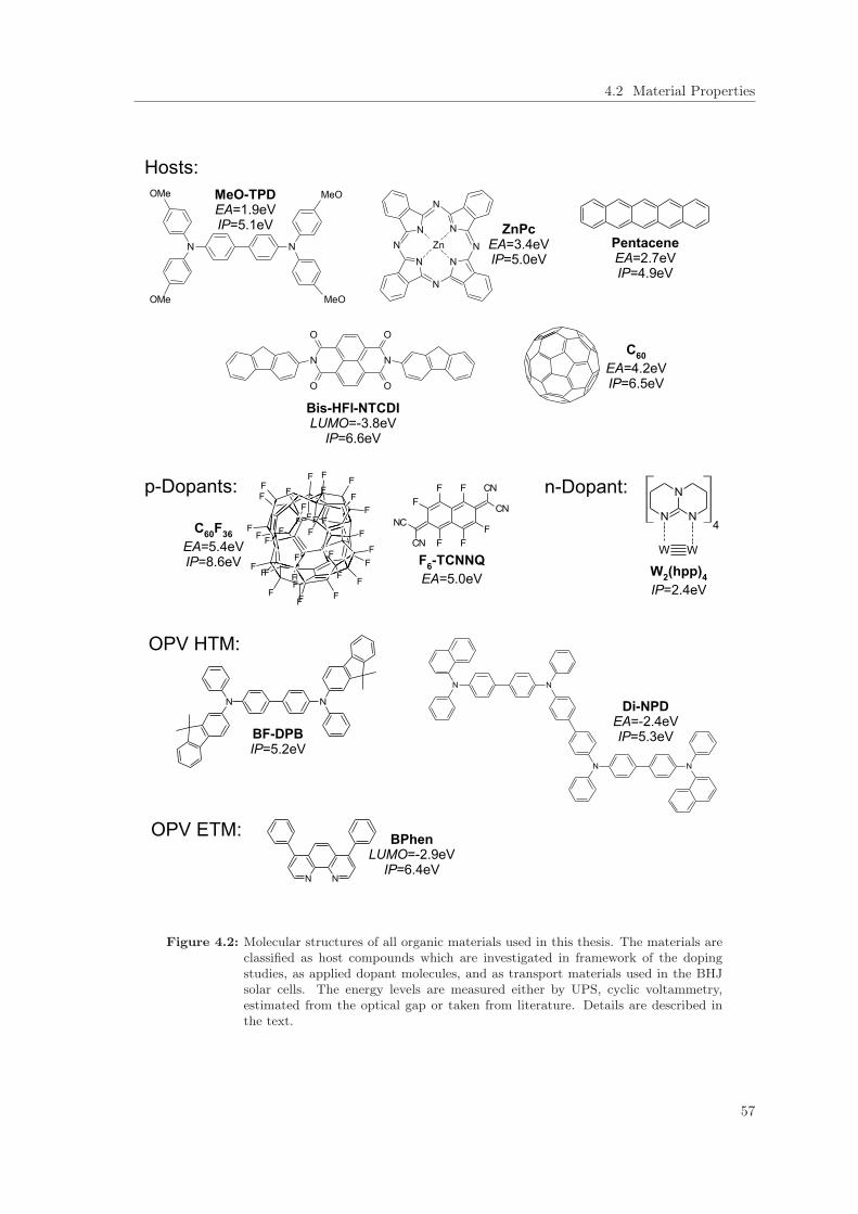
4.2 Material Properties
Figure 4.2: Molecular structures of all organic materials used in this thesis. The materials areclassified as host compounds which are investigated in framework of the dopingstudies, as applied dopant molecules, and as transport materials used in the BHJsolar cells. The energy levels are measured either by UPS, cyclic voltammetry,estimated from the optical gap or taken from literature. Details are described inthe text.
57

4 Experimental and Materials
4.2.2 Dopant Molecules
P-dopants: F6-TCNNQ, Fluorinated Fullerene C60F36, and NDP9
The p-dopant molecule 1,3,4,5,7,8-hexafluorotetracyanonaphthoquinodimethane (F6-TCNNQ) is struc-turally similar to the prominent acceptor molecule F4-TCNQ. However, F6-TCNNQ does show lessvolatility in vacuum, which makes this material to the more favored dopant. Its electron affinity hasbeen estimated to 5.00 eV by cyclic voltammetry7. F6-TCNNQ was purchased from Novaled GmbH(Dresden, Germany) and used as delivered.The fluorinated fullerene C60F36 possesses an electron affinity of 5.38 eV, [189] which makes it suitableas p-dopant for various hole transporting materials. [283] Due to its relatively large molecular massof 1404.6 g/cm3, doping concentrations by a factor of 4 lower than reachable with F6-TCNNQ arepossible. Furthermore, its volatility in vacuum is also uncritical. C60F36 was supplied by MTR Ltd.,USA, and used as delivered.The proprietary p-dopant compound NDP9 is an acronym for Novaled p-dopant No. 9 and has beenpurchased from Novaled GmbH (Dresden, Germany) and was used as received. During this thesis,it has been used for efficient p-doping of Di-NPB which was applied in solar cells as HTL.
N-dopant: Di-metal Complex W2(hpp)4
The di-metal complex of tungsten with the anion 1,3,4,6,7,8-hexayhydro-2H-pyrimido[1,2-a]pyrimidineW2(hpp)4 is used as n-dopant during this thesis. For the first time, it has been presented in 2002by Cotton et al. [198] and possesses an extremely low thin-film ionization potential of just 2.40 eVmeasured by UPS. Hence, it is unstable in air as powder, wherefore it has to be handled in inertatmosphere. W2(hpp)4 has been purchased from Novaled GmbH (Dresden, Germany) and is usedas delivered.
4.2.3 Transport Materials applied in Solar Cells
BPhen
4,7-diphenyl-1,10-phenanthroline (BPhen) is here applied as electron injection layer between C60 andaluminum within the solar cell of Ch. 7. It possesses an UPS ionization potential of 6.38 eV and anoptical gap of 3.52 eV. [273] Thus, its LUMO lies around -2.9 eV. In OLEDs BPhen is commonly usedas electron transport material, where it is n-doped by cesium. The thin-film density is 1.24 g/cm3.BPhen has been purchased from ABCR (Karlsruhe, Germany) and purified by CreaPhys GmbH(Dresden, Germany).
Di-NPD
N,N’-diphenyl-N,N’-bis(4’-[N,N-bis(naphth-1-yl)-amino]-biphenyl-4-yl)-benzidine (Di-NPD) is usedas hole transport material in the BHJ solar cells where it is p-doped by NDP9. It forms amorphousthin-films with an ionization potential of 5.33 eV and an optical gap of 2.9 eV. [284] The thin-filmdensity is given to 1.15 g/cm3. [285] Di-NPD has been supplied by Sensient (Wolfen, Germany) andpurified twice.7Measurement performed by Marion Wrackmeyer at the IAPP.
58

4.3 Fundamentals of Photoelectron Spectroscopy
BF-DPB
N,N’-Bis(9,9-dimethyl-fluoren-2-yl)-N,N’-diphenyl-benzidine (BF-DPB) is used as p-doped hole trans-port material in solar cells as well. It possesses a similar structure as MeO-TPD which differs only inthe side chains. Therefore, BF-DPB is expected to form completely amorphous thin-films. [283] Alsothe OFET mobility of 5.7 × 10⁻⁵ cm2/Vs is comparable to that of MeO-TPD8. However, the UPSionization potential is slightly higher: IP = 5.23 eV. The thin-film density of BF-DPB is 1.21 g/cm3.It has been purchased from Sensient (Wolfen, Germany) and purified twice per default by 3-zonevacuum gradient sublimation.
4.3 Fundamentals of Photoelectron Spectroscopy
4.3.1 Introduction to the Theory of the Photoelectron Emission Process
Photoelectron Spectroscopy (PES) is based on the external photo-effect, which has first been ob-served at the end of the 19th century. [286,287] Illuminating a grounded metal cathode by monochro-matic light causes anode photocurrents due to liberation of electrons, which can completely besuppressed by application of a retardation potential Uret. Here, Uret was found to scale linearly withthe frequency ν of the chosen light. Einstein explained the external photo-effect in 1905 by invokingthe quantum nature of light. [288] He proposed that the energy of one incident photon, E = hν, istransferred to at least one electron which can thus escape the metal surface, if its energy is sufficientto overcome the metal characteristic work function Φmetal. Hence, the maximum kinetic energy ofthe photoelectrons correlates directly with the retardation potential Uret and is given by
eUret = Ekin,max = hν − Φmetal . (4.1)
Consequently, the work function Φmetal and Planck’s constant h can be determined by varying theexcitation frequency ν and measuring Uret. In principle, modern Photoelectron Spectroscopy exper-iments are performed in a similar way, but using ideally monochromatic light sources and advancedelectrostatic analyzer systems for mapping the whole energy distribution Ekin of the emitted pho-toelectron spectrum. Hence, the electronic valence structure of a metal or semiconductor as well asthe characteristic binding energies of the respective atomic core levels can be resolved.
3-step Model and Basic Considerations. In a simple picture, the whole photoemission processcan be described as a 3-step process, [289] containing
i. local photoionization by photon absorption and excitation of an electron,
ii. traveling of the excited electron through the bulk to the surface, and finally
iii. escape of the electron through the surface into vacuum.
For the overall process, conservation of energy and momentum have to be fulfilled. Depending onthe type of experiment, i.e. investigating either core level or valence state photoemission, different
8Measured by Moritz P. Hein at the IAPP.
59

4 Experimental and Materials
boundary conditions are valid. In particular, various relevant interactions can influence the photo-electron spectra of the two different processes as well as their respective cross sections. Generally,the transition probability w between an initial Ψi and final state Ψf with the energies Ei and Ef isgiven by Fermi’s Golden rule
w ∝ 2π
�|〈Ψf |Δ|Ψi〉|2δ(Ef − Ei − �ω) , (4.2)
with the perturbation operator Δ of an incident electro-magnetic wave with the potential Φ andvector potential �A:
Δ =e
2mc( �A · �p+ �p · �A)− eΦ+
e2
2mc2�A · �A . (4.3)
Here, �p refers to the quantum mechanical momentum operator. In any case, the system is trans-ferred from an initial state with N to a final state with (N − 1) electrons and an additional freephotoelectron with the kinetic energy Ekin. Thus, for a solution of Eq. (4.2) appropriate multi elec-tron wave functions Ψi(N) and Ψf (N − 1) must be applied, depending on the type of experiment(valence or core level emission), e.g. Bloch states for UPS on a classical semiconductor. However,such calculations are rather complicated and out of focus of this thesis, therefore the reader is re-ferred to Ref. [289] for further information.
The Electron Mean Free Path. Typically, PES experiments are performed under UHV con-ditions and require atomistic clean sample surfaces. This experimental effort is necessary becausethe mean free path of electrons λ within solids is only in the order of a few Å. In other words,only electrons which are excited within the first monolayers of the sample can escape its surface andanalyzed by a detector. Actually, λ depends on the material (density) and the kinetic energy of anelectron (cf. Fig. 4.3), i.e. in case of a PES experiment on the excitation energy hν. For employingUPS (He-I: hν = 21.22 eV) to a thermally evaporated organic thin-film, λ is typically in the range of1...2 nm, whereas it is around 10 nm for XPS under AlKα irradiation (hν = 1486.65 eV). Therefore,any surface contamination has to be avoided in order to not distort the PES signal of the materialunder investigation. In particular, UHV conditions are mandatory to prevent surface contaminationupon physisorption of residuals during a PES experiment. One can estimate the time τML in secondsin which one monolayer is deposited on the sample surface at a certain vacuum pressure p (in mbar)to [289]
τML � 1.7× 10⁻⁶
0.6 · p ·S . (4.4)
Here, S = [0, 1] is a material combination specific sticking coefficient. For achieving coverage timesτML of several hours, a pressure of maximal p � 10−10 mbar is needed (assuming S = 1). Atp � 10−8 mbar, which is typical for the evaporation chambers, τML is only in the range of a fewminutes.However, the high surface sensitivity of PES can be very useful in several types of experiments. Inparticular, the energy level alignment at metal/organic and organic/organic interfaces as well aslevel bending effects can be studied on a sub-nanometer scale by stepwise deposition and UPS mea-surements. Furthermore, diffusion, depletion, or accumulation effects of dopant molecules within amatrix material or at a metal/organic contact as well as chemical interface reactions can be madevisible by XPS.
60

4.3 Fundamentals of Photoelectron Spectroscopy
Figure 4.3: Mean free path λ of an electron within different solids as function of its kineticenergy (taken from Ref. [289]).
Surface Effects. Due to the extreme surface sensitivity of PES, several surface effects appearwhich significantly can influence the shape of a measured spectrum but are not covered by thesimple 3-step model. Most importantly, the electronic surface structure of a molecular semiconduc-tor differs from its bulk-properties because missing molecules at the interface to vacuum effectivelyreduce the local electron density as well as the polarization energy. These effects usually lead to anincrease in the thin-film IP by a few 100 meV. [290,291] The next problem is that at the surface, thereis an abrupt change of the dielectric constant. Thus, ∇ �A �= 0, leading to the so-called surface pho-toelectric effect, e.g. visible as tailing features in valence spectra of Ag(111) surfaces. [292] Similarly,coupling of ∇A to a surface plasmon or of electrons to “softer” phonons at the surface might causeadditional peaks in valence PES spectra. [289]
Inverse Photoemission Spectroscopy (IPES). Here, the material under investigation is ir-radiated by electrons of defined (kinetic) energy Ei which are captured within the material byempty electronic states Ef . During this transition photons of the energy hν = Ei−Ef are releasedand further detected. Here, the measured photon spectrum correlates with the distribution of theun-occupied states of the material, e.g. with the conduction band structure of a semiconductor.
4.3.2 Details of the Experimental UPS/XPS Setup
General Spectrometer Description. The PES system used for this thesis is a Phoibos 100(Specs GmbH, Berlin, Germany) which is shown in Fig. 4.4. It is directly connected to the multichamber evaporation tool (UFO) and consists of an UHV analysis chamber, UV and X-ray sources,an electrostatic lens system, a hemispherical analyzer (HSA), and a multi channeltron detector(MCD). The standard excitations are the He-I line (21.22 eV) of a gas discharge lamp (SpecsUVS10/35, photon flux: 8 × 10¹⁵ (sr · s)−1 at a beam divergence < ±1◦) during UPS or charac-
61

4 Experimental and Materials
Figure 4.4: (a) Picture of the Phoibos 100 UPS/XPS system (Specs, Germany). (b) Illustrationof the analyzer main components and the voltage principle (tilted by 90◦, taken fromRef. [293]).
teristic AlKα (1486.65 eV) irradiation for XPS (Specs XR-50 ). Alternatively, the sample underinvestigation can be illuminated by He-II (40.8 eV) or MgKα X-rays (1253.64 eV). The base pressureof the analysis chamber is below 10−10 mbar. Ultra clean sample surfaces are achieved by in situAr+ sputtering. Sample cooling by liquid N2 flow through the sample holder as well as (re)heatingby underlying tungsten filaments is possible. Furthermore, the sample holder is rotatable within theplane spanned up by the excitation sources and the lens system.In principle, the photoelectrons which escape the sample surface are collected by the electrostaticlens system and guided to the entrance slit s1 of the HSA (cf. Fig. 4.4 (b)). If the kinetic energyEkin of the electrons fit to the (tunable) pass energy Epass of the HSA, they can reach its exit slit s2and be counted by the MCD, which finally yields an I(Ekin) spectrum. Both, the lens system andthe (entrance and exit) slit sizes affect the energy spread detected by the analyzer. Furthermore,the lens stage defines the analysis area (measurement spot size) and angular acceptance by imagingthe emitted photoelectrons on the input slit s1 as well as retarding/accelerating them to Epass forsubsequent energy analysis. The energy analyzer system as well as the MCD are controlled bya HSA3500 high-voltage power supply which is connected via a CAN-Bus and a CAN-EthernetAdapter (Specs EC10 ) to a PC. The complete functionality of the Phoibos 100 system is managedby the delivered software SPECsLab. In the following, the individual parts and their impact on themeasured spectra (energy resolution) will be briefly presented.
Lens System Phoibos. The lens system consists of 10 (T1 . . . T10) electrostatic lenses as well asan additional entrance Iris. During measurements, the sample must be located in the focal plane ofthe lens system which is 40 mm in front of the first lens electrode T1. Furthermore, the photoelec-trons traveling through the lens system are decelerated by the potential U0 which is linked by thepassing condition eU0 = Ekin −Epass to detection of the electrons by the MCD. Hence, the Phoibos
62

4.3 Fundamentals of Photoelectron Spectroscopy
can be operated in two different ways called Fixed Retarding Ratio (FRR) or in Fixed AnalyzerTransmission (FAT) modes. In the latter case, the retardation potential U0 is swept such thatall photoelectrons pass the HSA at a fixed pass energy Epass independent of their kinetic energy.In contrast, when applying the FRR mode all photoelectrons are decelerated with the same fixedfactor R defined by Epass = Ekin/R, i.e. the pass energy is not fixed. However, since the energyresolution of the HSA depends on Epass (cf. Eq. 4.6) only FAT modes are applied during this the-sis for UPS/XPS experiments. The different available transmission modes are controlled by presetlens voltages (not adjustable by the user) and optimized for high transmission at different spot sizes.
Hemispherical Analyzer (HSA). A radial electric field between the two hemispheres forcesthe electrons entering the HSA through the slit s1 onto elliptical trajectories with the mean radiusr0 = 100mm. The radii of the inner and outer hemispheres are rIH = 0.75 r0, and rOH = 1.25 r0,respectively. Thus, electrons with an energy of
Epass = −ek(UOH − UIH) with: k =rINrOH
2r0(rOH − rIN)= 0.9375 (4.5)
pass the hemispherical capacitor exactly on the central circular trajectory r0. Here, UOH − UIH
refers to the voltage difference between the outer and inner hemisphere. Depending on the typeof experiment (excitation energy), four different ranges for the (high) voltages VOH, VIH as well asthe retardation voltage U0 are adjustable, affecting the measurement accuracy, e.g. 0.1 meV for the0 . . . 40 eV range. The width of a transmitted line ΔEHSA further depends on the pass energy aswell as on the sizes of the applied slits and is given by [293]
ΔEHSA = Epass
(s
2r0+
α2
4
)with: s =
s1 + s2
2. (4.6)
Here, s indicates a slit specific constant and α the angle under which the electrons reach the detector.It is obvious that the energy resolution of the analyzer increases with the hemispherical radius r0
and decreases with the pass energy Epass. However, the value of Epass does further affect the signalintensity I(Ekin). In case of a FAT lens mode, it decreases with the kinetic energy by I ∝ 1/Ekin, [293]
whereas the analyzer resolution ΔEHSA is constant for all energies.Additional broadening of a line occurs due to the inherent line width of the excitation sourceΔEphoton (e.g. AlKα) and the width of the atomic level ΔElevel (e.g. C1s). Thus, the overall fullwidth at half maximum can be estimated to
FWHM =√ΔE2
HSA +ΔE2photon +ΔE2
level . (4.7)
Probing an Ag3d5 level by AlKα excitation yields a best value for the FWHM=0.44 eV.
Multi Channeltron Detector (MCD). For final electron counting the system is equippedwith a MCD (Specs PCU 300 ) consisting of five channeltrons C1 . . . C5. These glass tubes are cov-ered with a high resistance material (about 50MΩ) which act as continuous dynodes if a potentialdifference is applied between the ends of the tubes. The applied voltage must be high enough toguarantee operation of the channeltrons in saturation and is around 3 kV, yielding typical gains in
63
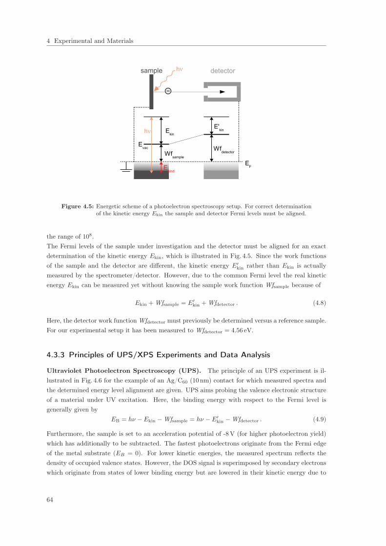
4 Experimental and Materials
ν
ν
Figure 4.5: Energetic scheme of a photoelectron spectroscopy setup. For correct determinationof the kinetic energy Ekin the sample and detector Fermi levels must be aligned.
the range of 108.The Fermi levels of the sample under investigation and the detector must be aligned for an exactdetermination of the kinetic energy Ekin, which is illustrated in Fig. 4.5. Since the work functionsof the sample and the detector are different, the kinetic energy E′kin rather than Ekin is actuallymeasured by the spectrometer/detector. However, due to the common Fermi level the real kineticenergy Ekin can be measured yet without knowing the sample work function Wfsample because of
Ekin + Wfsample = E′kin + Wfdetector . (4.8)
Here, the detector work function Wfdetector must previously be determined versus a reference sample.For our experimental setup it has been measured to Wfdetector = 4.56 eV.
4.3.3 Principles of UPS/XPS Experiments and Data Analysis
Ultraviolet Photoelectron Spectroscopy (UPS). The principle of an UPS experiment is il-lustrated in Fig. 4.6 for the example of an Ag/C60 (10 nm) contact for which measured spectra andthe determined energy level alignment are given. UPS aims probing the valence electronic structureof a material under UV excitation. Here, the binding energy with respect to the Fermi level isgenerally given by
EB = hν − Ekin −Wfsample = hν − E′kin −Wfdetector . (4.9)
Furthermore, the sample is set to an acceleration potential of -8V (for higher photoelectron yield)which has additionally to be subtracted. The fastest photoelectrons originate from the Fermi edgeof the metal substrate (EB = 0). For lower kinetic energies, the measured spectrum reflects thedensity of occupied valence states. However, the DOS signal is superimposed by secondary electronswhich originate from states of lower binding energy but are lowered in their kinetic energy due to
64
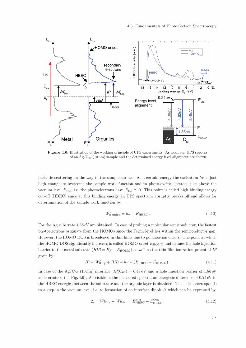
4.3 Fundamentals of Photoelectron Spectroscopy
Δ
ν
Δ
Figure 4.6: Illustration of the working principle of UPS experiments. As example, UPS spectraof an Ag/C60 (10 nm) sample and the determined energy level alignment are shown.
inelastic scattering on the way to the sample surface. At a certain energy the excitation hν is justhigh enough to overcome the sample work function and to photo-excite electrons just above thevacuum level Evac, i.e. the photoelectrons have Ekin � 0. This point is called high binding energycut-off (HBEC) since at this binding energy an UPS spectrum abruptly breaks off and allows fordetermination of the sample work function by
Wfsamlpe = hν − EHBEC . (4.10)
For the Ag substrate 4.38 eV are obtained. In case of probing a molecular semiconductor, the fastestphotoelectrons originate from the HOMOs since the Fermi level lies within the semiconductor gap.However, the HOMO DOS is broadened in thin-films due to polarization effects. The point at whichthe HOMO DOS significantly increases is called HOMO-onset EHOMO and defines the hole injectionbarrier to the metal substate (HIB = EF −EHOMO) as well as the thin-film ionization potential IPgiven by
IP = WfOrg + HIB = hν − (EHBEC − EHOMO) . (4.11)
In case of the Ag/C60 (10 nm) interface, IP(C60) = 6.48 eV and a hole injection barrier of 1.86 eVis determined (cf. Fig. 4.6). As visible in the measured spectra, an energetic difference of 0.24 eV inthe HBEC energies between the substrate and the organic layer is obtained. This effect correspondsto a step in the vacuum level, i.e. to formation of an interface dipole Δ which can be expressed by
Δ = WfOrg −WfMet = EMetHBEC − EOrg
HBEC . (4.12)
65

4 Experimental and Materials
In conclusion, only the HOMO and HBEC region of an UPS spectrum are relevant for this thesis.The corresponding values EHOMO and EHBEC are obtained by fitting a line to the rising signal flankand determining the intersection with the background. The energy broadening during UPS hasbeen estimated by measurement of the width of a gold Fermi edge, which is 120 meV between 90%and 10 % intensity, to just 10 meV. [273] However, the experimental error due to reproducibility (e.g.sample preparation) has been estimated to 50meV.For each UPS spectrum, the emission features due to the secondary line excitations of the He-I gasdischarge are subtracted. The considered satellites of the He-I discharge lamp are 23.09 eV (≈ 2.5%),23.75 eV (≈ 0.3%), and 24.05 eV (≈ 0.15%). Since the actual relative intensities of the satellite ex-citations depend on the He discharge pressure, the secondary line sub-spectra are adjusted slightlyin intensity to the measured UPS spectrum (gap region) and subtracted incrementally starting withthe 24.05 eV satellite.The measurement times are kept as short as possible to avoid effects due to UV degradation of theorganic materials and are typically below 10 minutes for a complete UPS measurement. The kineticenergies are scanned in steps of 0.01 eV (each 0.1 s dwell time) at a fixed pass energy of Epass = 3 eV
to increase the energy resolution. The HOMO region of a spectrum is furthermore scanned in theLow Angular Dispersion lens mode (1.2 mm2 spot size).
X-ray Photoemission Spectroscopy (XPS). The principle of a XPS experiment is illustratedin Fig. 4.7. The photoemission process is generally similar to UPS, however, due to the higher exci-tation energy (AlKα: 1486.65 eV) electronic states with much higher binding energy are accessibleby XPS. In particular, the characteristic core levels (e.g. C1s, N1s) of atoms which are contained inthe molecules of an organic thin-film can be analyzed in detail.As example, a complete survey scan of a 15 nm DCV-4T-Me(1,1,4,4) film on Au is shown in Fig. 4.7.The individual measured peaks correspond to the carbon, nitrogen, and sulfur atoms in thesemolecules. Additionally, the characteristic Au4f double peak of the underlying substrate is visi-ble at EB ≈ 90 eV. Since scanning the whole range of energies takes up to several hours, a surveyscan is typically used just for a rough element check and the individual element peaks are addi-tionally scanned with a higher energy resolution by applying a suitable lens mode. This allows fora detailed analysis of the bounding conditions within a molecule. As example, the W4f and N1ssignals of a pure 4 nm W2(hpp)4 thin-film evaporated on Au are additionally shown in Fig. 4.7. TheN1s peak consists of two sub-peaks with relative intensities of 1:2 since two of the nitrogen atomsare involved in binding of the (hpp) "paddles" to the W2 core of the molecule, while the remainingnitrogen atom within an (hpp) paddle is just bound to carbons. The W4f peak is also split up into tosub-peaks, however, the reason here is the spin-orbit coupling of the f-level electrons to j = |l ± s|.According to quantum mechanics, the degeneracy in energy is 2j + 1, i.e. for l = 3 and s = 1/2 itis 6 for j = 5/2 and 8 for j = 5/2. Thus, the level is split into W4f5/2 : W4f7/2 = 3 : 4 sub-peaks.Correspondingly, p- and d-levels are split into 1:2 and 2:3 doublets, respectively, whereas s-levels areusually single peaks. Due to the mechanism of spin-orbit coupling, the energetic splitting increaseswith the element number.For XPS peak fitting, the symmetric Gaussian-Lorentzian sum function
I(E) ∝ (1−m) exp[−ln(2)x2] +m1
1 + x2with: x =
2(E − E0)
w(4.13)
66

4.3 Fundamentals of Photoelectron Spectroscopy
ν
Δ
Figure 4.7: Illustration of the working principle of a XPS experiment. As example, a surveyscan of an Au/DCV-4T-Me(1,1,4,4) (15 nm) as well as the individual W4f and N1speaks of an Au/W2(hpp)4 (4 nm) sample are shown.
is used, where E0 refers to the energetic peak position, w to its width and m = [0, 1] defines theLorentzian to Gaussian (L:G) ratio. Typically, ratios in the order of 40 % and peak FWHMs ofabout 1.5 eV are obtained. Additionally, a linear or Shirley-type background is assumed.Absolute peak intensities between different samples/measurements are difficult to compare sincethey depend on various factors, e.g. applied lens mode, film density, and measurement geometry.However, relative peak intensities of different elements within on sample/measurement can reliablybe compared, if the respective cross sections of the photoionization processes are known. These areexpressed by so-called relative sensitivity factors (RSF) which are normalized to C1s (RSF = 1), andmust be multiplied to the measured intensities. For an ultra-precise analysis, the RSF factors haveto be determined individually for a XPS setup by using a reference sample since they depend onthe measurement geometry. However, in this thesis it is sufficient to use literature values publishedfor a similar geometry. [294]
During the experiments, the X-ray source is usually operated at a power of 270 . . . 300W. The passenergy is typically set to Epass = 20 eV and for the peak scans, the Large Area lens mode is used,which corresponds to a spot size of 5 mm2. The kinetic energy is scanned in 0.05 eV steps (each 0.1 sdwell time) and the peaks are integrated over a up to 240 scans, depending on the overall intensity.
67

4 Experimental and Materials
4.4 Other Characterization Techniques
4.4.1 Conductivity
If not differently stated, the conductivity measurements are performed in situ, i.e. during thin-filmdeposition in vacuum at the UFO. Glass substrates covered with 50 nm thick silver contacts areused. The silver has been thermally evaporated through a shadow mask of meander type structure.During evaporation of the doped organics the sample is biased by V = 10V and the lateral currentI through the semiconductor is logged versus the deposited film thickness d. The conductivity isthen given by
σ =I
V
l
b · d . (4.14)
Here, l refers to the distance and b to the widths of the silver contacts. To resolve very low filmconductivities, the l/b aspect ratio has to be kept as small as possible, e.g. 0.5mm/111mm = 0.0045
for the meander type contact structure. The current is measured by a Keithley Source Measure Unit236. Finally, the conductivity is determined from the slope of I vs. d plots. Further experimentaldetails are described in the diploma thesis of Kathleen Schmidt. [295]
4.4.2 Impedance Spectroscopy
Schottky diodes are investigated by impedance spectroscopy to determine the doping properties ofthe used organic semiconductors. Here, the phase shifted current response
i(t) = Ibias + IS sin(ωt+ ϕ) (4.15)
on an applied voltage Vbias which is superimposed by an AC small signal
v(t) = Vbias + VS sin(ωt) (4.16)
is measured over a frequency range of 10 Hz to 1MHz. The complex impedance Z = �(Z) + j �(Z)
of the device is then given by
�(Z) =VS
IScos(ϕ) ; �(Z) =
VS
ISsin(ϕ) . (4.17)
For a pure capacitive device, the phase is ϕ = −90◦, �(Z) = 0, and the imaginary part linked tothe capacitance C by
�(Z) = − 1
ωC. (4.18)
However, at too high doping concentrations the investigated ITO/p-MeO-TPD/aluminum structuresshow considerable resistive behavior. Therefore, the measured impedance is fitted by a suitableequivalent circuit for determination of the depletion capacitance CP of the Schottky contact (cf.Sec. 5.1.3). The measurements are performed in dark with an Autolab PGSTAT302N (MetrohmAutolab, Netherlands). The probe signal VS has an amplitude of 10mV (rms) and the bias signalVbias is varied from 0.5 to −1.0V.
68

4.4 Other Characterization Techniques
4.4.3 Laser Desorption Ionization - Time of Flight - Mass Spectroscopy
The composition of organic thin-films can be analyzed by Laser Desorption Ionization - Time ofFlight - Mass Spectroscopy (LDI-TOF-MS). Here, the sample under investigation is excited by laserpulses of comparably high power, which detaches complete molecules from the thin-film. Furtherionization and subsequent mass spectroscopy allow for conclusions on the film composition.The LDI-TOF-MS measurements are performed by a Bruker Daltonics Autoflex TOF/TOF tandemmass spectrometer. As substrates 50 nm thermally evaporated gold on glass pre-covered with athin aluminum layer are used. The substrates are grounded and an acceleration voltage of 19 kV isapplied between the sample and the aperture of the TOF analyzer. The samples are excited by aN2 laser (337 nm) with 3 . . . 5 ns pulses and a spot size of 0.01 mm2. Here, the laser intensity is setsuch that there is sufficient signal but no fracturing of the molecules (120mJ, cf. Sec.9.1). The LDI-TOF-MS signal is integrated over 30 laser pulses, however, already 10 . . . 12 pulses are sufficient todesorb all the organic material from one spot area (cf. Sec. 9.1). The samples are transferred fromUFO via an air tight box to the LDI-TOF-MS chamber within less than 50 s of handling in air.Further details of the experimental setup are described elsewhere. [296]
4.4.4 Solar Cell Characterization
The solar cells are characterized under (constant) room temperature applying the sun simulator16S-150 V3 from the Solarlight Company Inc. (Glenside, US) and a Keithley 2400 Source MeasureUnit (LIV-robot of the IAPP). The light from the sun simulator is guided via a glass fiber to thesample surface. For spectral mismatch correction, the (effective) illumination intensity of the sunsimulator can be set to the desired value with respect to a calibrated reference diode. All solar cellsare measured with an assumed spectral mismatch of 0.79, however, the actual mismatch factors ofthe ZnPc:C60 solar cells with varied blend ratios are in between 0.764...0.799, which results in avariation of the effective illumination intensity by a maximum of 3.5%. The corresponding errorimpact on VOC is estimated by Eq. (3.51) (on page 52) to be < 1mV and hence negligible. Thedominant error contribution to determination of VOC is due to interpolation of the j-V characteristicsto j = 0, and estimated to ±7mV.
4.4.5 Grazing incidence X-Ray Diffraction
The crystallinity of organic thin-films can be measured by X-ray diffraction. This analysis method isbased on the elastic scattering of coherent X-ray beam at atoms or molecules, leading to interferenceeffects for periodic structures. The diffraction angle θ is linked to the lattice plane distance a bythe Bragg condition
nλ = 2a · sinθ . (4.19)
Here, n refers to the interference order and λ to the wavelength of the X-rays. Typically, theincidence angle is fixed and the detection angle θ is varied. Decreasing the incidence angle yields aconsiderable improvement in the signal to noise ratio since the scattering volume is increased.The grazing incidence X-ray diffraction (GIXRD) experiments are performed by Lutz Wilde at theFraunhofer CNT (Dresden, Germany) with a Bruker D8 Discovery diffractometer. It uses Cu-Kα1
radiation monochromatized by a secondary graphite monochromator. The X-rays is guided via a
69

4 Experimental and Materials
Göbel mirror on the organic thin-film with an incidence angle of 0.17 . . . 0.21◦. The detection angle2θ to the scintillation detector is varied in 0.1◦ steps.
4.4.6 Fourier-Transform Photocurrent Spectroscopy
Fourier-Transform photocurrent spectroscopy (FTPS) is used during this thesis for high resolutionmeasurements of the low energy tail of the external quantum efficiency (EQE) of organic solar cells.The measurements are performed by Koen Vandewal at Linköping University (Sweden). There, aresearch grade Fourier-Transform infrared spectrometer (Bruker Vertex 70 FTIR), adjusted for usein the visible and near IR wavelength range by application of a quartz tungsten halogen (QTH)light source and a quartz beamsplitter, is used. The modulated light beam, exiting the Michelsoninterferometer of the FTIR, is focussed onto the photovoltaic device. The photocurrent producedby this excitation light under short-circuit conditions is amplified by a low noise current amplifier(Stanford Research SR570) and the amplified electrical signal is fed back into the FTIR. In thisway, the FTIR software considers the solar cell to be measured as an external detector, and alldata corrections and Fourier-Transform are performed by the software delivered with the FTIR.The spectral dependence of the QTH lamp is taken into account and divided out. It is measuredpreviously in the same way as described above, but with a reference Si or Ge photo-diode withknown spectral response. Further details on the FTPS technique can be found in Ref. [297]
70

5 | Investigations on Molecular p-Doping
The results of systematic UPS measurements on various p-dopant:host combinationswill be presented in this chapter. In this context, the Fermi level shift versus thedoping concentration as well as the doping efficiency are experimentally determined.First, a comprehensive study on molecular p-doping of MeO-TPD summarizes themain findings and correlations. For explanation, a statistical doping model is de-veloped and applied to the measurement data. In particular, it is shown that at lowdoping concentrations molecular doping is hindered by deep trap states. These find-ings are finally extended to p-doped ZnPc and pentacene thin-films, yielding similarresults. Here, the molar doping ratios are reduced to 10−4 . . . 10−5 to show evidencefor dopant saturation and reserve regimes.
5.1 P-Type Doping of MeO-TPD by C60F36 and F6-TCNNQ
5.1.1 Fermi Level Position versus Doping Concentration
P-type doping of the common hole transport material MeO-TPD is investigated by UPS, usingthe dopant molecules C60F36 or F6-TCNNQ. Doped thin-films are evaporated directly on a sputtercleaned silver foil with a work function of Wf(Ag) = 4.3 eV. The thicknesses of the organic films(10 . . . 20 nm) are larger than the expected space charge layer widths of the obtained Schottky con-tacts, which are typically in the range of 2 . . . 12 nm. A series of samples with doping concentrationsranging from MR ≈ 0.0009 to 0.5 is fabricated. Here, the lowest reachable concentration is limitedby the resolution of the dopant QCM and a maximal deposition rate of 2Å/s for MeO-TPD. Apartfrom that, the host material is usually deposited with rates of 0.3 . . . 0.4Å/s.In Fig. 5.1 representative UPS spectra of MeO-TPD thin-films p-doped by C60F36 (a) or F6-TCNNQ(b) are shown. The HOMO-onsets of the spectra are indicated by circles. The energetic differenceto the Fermi level (EBind = 0) is defined as hole injection barrier from the underlying Ag substrateto the doped organic film. With increasing doping concentration the spectra are shifted to lowerbinding energies, i.e. the Fermi level moves towards the MeO-TPD HOMO and the hole injectionbarrier decreases. Simultaneously, the high binding energy cut-off (HBEC) shifts to lower bindingenergies, i.e. the organics work function, defined as the difference between the Fermi and the vacuumlevel, increases.Rescaling the energy axis such that the HOMO-onset of MeO-TPD is at 0 eV defines the correspond-ing Fermi level position with respect to the HOMO-onset. This quantity is plotted versus the dopingconcentration in Fig. 5.2 (a). Additionally, data for the material combination MeO-TPD:F4-TCNQ
71

5 Investigations on Molecular p-Doping
Figure 5.1: UPS spectra of MeO-TPD thin-films evaporated on Ag-foil and p-doped by C60F36
(a) or F6-TCNNQ (b). The molar doping ratio is varied between 0.0009 and 0.52.The HOMO-onsets are indicated by circles.
published by Olthof et al. [11] are given. Interestingly, the shape of the obtained curves are sim-ilar for C60F36 and F6-TCNNQ, but different in comparison to the system MeO-TPD:F4-TCNQ.In case of C60F36, four characteristic regions can be identified. For MR < 10−3 the Fermi levelremains close to the intrinsic value of around 1.7 eV above the HOMO-onset (gray bar). Between10−3 < MR < 10−2, a strong shift of the Fermi level by approximately 0.9 eV is found, followed bya much weaker shift until EF = 0.32 eV at a molar doping ratio of about 10−1. For even higherconcentrations, a kind of Fermi level pinning is observed. Taking the measurement inaccuracies intoaccount, the obtained Fermi level positions of MeO-TPD:F6-TCNNQ samples are equal, at least forMR > 0.007.Qualitatively similar observations were reported for the system MeO-TPD:F4-TCNQ. However, thepinning energy is slightly higher (0.35 eV), and the characteristic strong shift of the Fermi leveloccurs at doping concentrations of roughly one order of magnitude higher, i.e. in the range of7 × 10−3 < MR < 7 × 10⁻². This result is remarkable since it means that at high concentrations,the number of free charge carriers provided by doping is approximately equal for all three dopants.However, already at medium concentrations the doping effect of F4-TCNQ is expected to be muchweaker than for C60F36 and F6-TCNNQ because the Fermi level is located deeper in the gap byseveral 100 meV. At very low concentrations below MR < 10−3, molecular doping is expected notto work at all.
72

5.1 P-Type Doping of MeO-TPD by C60F36 and F6-TCNNQ
Figure 5.2: (a) Fermi level position of p-doped MeO-TPD thin-films on Ag using differentmolecular p-dopants. The data for F4-TCNQ are taken from Ref. [11] EF = 0 refersto the position of the HOMO-onset of the respective UPS spectrum.(b) Corresponding conductivity data, the values are taken from Ref. [11,283]
For a more comprehensive interpretation of the UPS results, room temperature conductivity data ofp-doped MeO-TPD films are shown in Fig. 5.2 (b). The values are taken from Ref. [11,283] and weremeasured in lateral geometry at the IAPP. A different trend than for the UPS data is found. Theconductivities of films doped by F6-TCNNQ and F4-TCNQ are practically equal for the whole rangeof doping concentrations. In agreement with values obtained by applying C60F36, a linear correla-tion between the conductivity and the molar doping ratio can be identified at low concentrations(slope=1). However, above concentrations of MR > 10−2, this correlation becomes super-linearfor F6-TCNNQ and F4-TCNQ, and sub-linear for C60F36. The maximum conductivities at highmolar doping ratios are apart by two orders of magnitude, reaching approximately 2 × 10⁻³ S/cm
for F4-TCNQ and 4 × 10⁻⁵ S/cm for C60F36. Menke et al. attributed the relatively low con-ductivities in the latter case to the large molecule size of C60F36 which might disturb thin-filmformation of the host material at high concentrations and reduce the hole mobility. [283] However,since even undoped MeO-TPD thin-films are completely amorphous,1 possessing a low mobility of3.5 × 10−5 cm2/Vs,2 a further reduction of the mobility upon structural changes seems unreason-able. It might be more plausible that the large amount of dopant molecules at concentrations aboveMR = 0.2 simply occupies so much space that the number of reachable hopping sites for a hole(MeO-TPD molecules) is reduced, causing the mobility drop. Against this argumentation speaksthe fact that the conductivity-concentration correlation becomes sub-linear already at molar dopingratios of only 0.01 . . . 0.05.Menke et al. published Seebeck measurement data on the same host:dopant systems as well. [283]
The positive Seebeck energy ES , which corresponds to the distance of the Fermi level to an averagecharge carrier transport level of holes, ES = ETr − EF , also decreases with increasing doping con-
1Confirmed by GIXRD measurements.2Measured by Moritz P. Hein in OFET geometry at the IAPP.
73

5 Investigations on Molecular p-Doping
centration, clearly indicating a p-doping effect. In agreement with the UPS data of Fig. 5.2 (a), theobtained Seebeck energies are almost equal for MeO-TPD doped by either C60F36 or F6-TCNNQ.In a semi-logarithmic plot ES decreases linearly with the doping concentration from approximately200...50 meV over a range of molar doping ratios from MR = 0.005 . . . 0.4 for both dopants. [283] Thisresult supports the hypothesis that the actual charge carrier generation efficiency is similar or evenequal for C60F36 and F6-TCNNQ doped into MeO-TPD, which furthermore explains the similarconductivities at low doping concentrations (cf. Fig. 5.2 (b)). However, the very strong shift of theFermi level of about several 100 meV (cf. Fig. 5.2 (a)) is not confirmed by the Seebeck data. TheSeebeck energy also does not saturate at high concentrations, which is also in contradiction to theUPS results. An explanation for these discrepancies would be that the average hole transport levelETr also shifts with rising doping concentrations from deep states to states closer to the HOMOcenter.To get a deeper insight into the physics of the doping process, the doping efficiency has been mea-sured with UPS, which is described in the next section.
5.1.2 Resolving Depletion Layer Thicknesses: Estimating the DopingEfficiency
The doping efficiency can be estimated from the space charge layer (SCL) width of a Schottkycontact (cf. Sec. 3.4.1). However, due to varying sticking coefficients of dopant molecules on dif-ferent substrates, it has been suggested to introduce a thin intrinsic interlayer between the metalsubstrate and the p-doped layer to guarantee a homogeneous doping profile over the whole spacecharge layer. [184]
For illustration, doping profiles of a simple Schottky contact as well as of a corresponding m-i-p3
structure are compared in Fig. 5.3 (a) for MeO-TPD doped by C60F36. The molar doping ratio(intended: MR = 0.2) has been determined by XPS, i.e. by comparing the F1s and O1s peak inten-sities. In case of the simple Schottky contact a depletion of dopants close to the metal substrate bya factor of two is found, however, the intended ratio of MR = 0.2 is reached after an organic thick-ness of 3 nm. The effect of dopant depletion can be completely avoided by introducing the intrinsicinterlayer (d = 5nm). Here, the intended doping ratio is ensured already for layer thicknesses of thedoped film of x < 1 nm. The variations in Fig. 5.3 (a) are only due to experimental uncertainties.Hence, the favorite sample structure for this kind of experiments is a so-called m-i-p stack (cf.Fig. 5.3 (b)). The corresponding energy level bending is sketched in Fig. 5.3 (b). Under the abruptapproximation
ρ(x) =
⎧⎪⎪⎪⎨⎪⎪⎪⎩0 , 0 < x < x1
−eN−A , x1 < x < x2
0 , x > x2 ,
(5.1)
the electric field and potential are calculated for x1 < x < x2 analogously to common Schottkycontacts to
F (x) =eN−
A
ε0εr(x2 − x) ; V (x) =
eN−A
2ε0εr(x− x2)
2 . (5.2)
3metal/intrinsic/p-doped structure
74

5.1 P-Type Doping of MeO-TPD by C60F36 and F6-TCNNQ
Δ
Δ
Figure 5.3: (a) Comparison of doping profiles in MeO-TPD:C60F36 films deposited either di-rectly on Ag or on an intrinsic interlayer. (b) Schematic energy level bending formetal/intrinsic/p-doped structures. Intrinsic interlayer thicknesses of d = 3 . . . 5 nmare applied in the UPS samples.
For the undoped interlayer, 0 < x < x1, the electric field is constant and determined by the boundarycondition at x1 to
F (x) =eN−
A
ε0εr(x2 − x1) . (5.3)
Thus, the electric potential drops linear:
V (x) = −eN−A
ε0εr(x2 − x1)x+
eN−A
2εeεr(x2
2 − x21) . (5.4)
By substituting x1 = d and x2 = w+d as well as considering the boundary condition V (x = 0) = ΔV ,one finally obtains
N−A =
2ε0εrΔV
e(w2 + 2wd). (5.5)
Here, ΔV is the built-in potential of the m-i-p structure, d the intrinsic interlayer thickness, and w
the space charge layer width of the p-doped region.
Six p-doped MeO-TPD samples using C60F36 and varying the molar doping ratio in the rangeof 0.0009 and 0.31, as well as four samples with F6-TCNNQ and MR = 0.008 . . . 0.14, are investi-gated by UPS. UPS spectra of four representative MeO-TPD:C60F36 samples are shown in Fig. 5.4.The organic layers have been deposited stepwise, e.g. in sub-nanometer steps. After each deposi-tion, the UPS spectra are taken. With increasing (cumulated) thickness x of the p-doped layers,the spectra are shifting to higher binding energies until the final positions outside of the depletionzones are reached. The determined Fermi level positions versus the thicknesses x are summarized inFig. 5.5 for all samples. It is clearly visible that the depletion width decreases with increasing dopingconcentration to only a few nanometer at molar ratios above 0.1. However, it has to be emphasizedthat these plots do not directly coincide with the assumed level (potential) bending due to presenceof the intrinsic interlayers. Nonetheless, the space charge layer thicknesses w can be determinedcorrectly from these graphs, which is indicated by red lines. The obtained space charge layer widthsw, final Fermi level positions EF in the doped layers (i.e. for x ≥ w), as well as the built-in potentials
75

5 Investigations on Molecular p-Doping
Figure 5.4: UPS spectra of Ag/MeO-TPD(d = 3 . . . 5 nm)/MeO-TPD:C60F36 samples whichhave incrementally been evaporated and measured. The numbers indicate the cu-mulated thickness x of the p-doped layer.
ΔV are listed in Tab. 5.1. Here, the built-in potential is defined as ΔV = EF (x = 0)−EF (x ≥ w).EF (x = 0) refers to the Fermi level position of the intrinsic buffer layer and is typically around1.7 eV. The dielectric constant is assumed to be εr = 3. Finally, the doping efficiencies ηdop = p/NA
are calculated by Eq. (5.5), assuming p = N−A and NA = MR × N0 with the number density of
matrix molecules per volume N0 = 1.45× 1021 cm−3.At high molar ratios, the doping efficiency p/NA is in the range of 4 . . . 7% and thus comparable tothe reported values of MeO-TPD:F4-TCNQ films. [11] However, the fraction of ionized dopants in-creases with decreasing doping concentration for both dopants likewise up to a value of around 36%for C60F36 at MR = 0.00088. So far, this is the highest reported value for molecular p-type dopingmeasured with UPS/XPS. Furthermore, the data show that the depletion layer thicknesses as well asthe doping efficiencies are approximately equal for both dopants at a certain molar ratio (within theexperimental error). For example, the depletion width is w = (9 ± 1) nm for MR(C60F36) = 0.007
and MR(F6−TCNNQ) = 0.008, which leads to similar efficiencies of p/NA ≈ 21%. Thus, it isconcluded that the underlying doping process should be equal for both acceptors and is not lim-ited by the dopants as it seems to be the case for F4-TCNQ. This assumption is supported by thematching Fermi level positions for F6-TCNNQ and C60F36 doped films, whereas EF lies close to theundoped position for F4-TCNQ at MR ≈ 0.007 (cf. Fig. 5.2 (a)). However, without special tricks,a controlled co-evaporation of MeO-TPD and F6-TCNNQ at lower doping concentrations is notpossible due to the relatively low molar mass of the dopant. Thus, at this point we can only assumethat the Fermi level shift and doping efficiency matching is also true for smaller concentrations.
76

5.1 P-Type Doping of MeO-TPD by C60F36 and F6-TCNNQ
However, the system MeO-TPD:C60F36 can be considered so far as a representative prototype sys-tem, demonstrating an intrinsically hindered doping process. Hence, Mott-Schottky analysis hasbeen performed at MeO-TPD:C60F36 diodes, which will be addressed in the following.
Figure 5.5: Evolution of the Fermi level position versus the thickness x of the p-doped layerof Ag/MeO-TPD(d = 3 . . . 5 nm)/p-MeO-TPD structures, applying C60F36 (a) orF6-TCNNQ (b) as p-dopant. The black lines are for guidance to the eye. The redlines indicate the estimated space charge layer widths w.
dopant MR d w EF eΔVp/NA(nm) (nm) (eV) (eV)
C60F36
0.00088 2.9 12± 2 1.38 0.30 0.3640.0042 3.1 10.5± 1.0 0.63 1.06 0.3260.0070 5.0 9± 1 0.54 1.20 0.2290.0117 5.8 7.5± 1.0 0.46 1.32 0.1800.0691 5.1 3.1± 0.5 0.38 1.29 0.1030.3125 4.9 2.1± 0.4 0.32 1.43 0.042
F6-TCNNQ
0.0084 4.3 9± 1 0.53 1.17 0.2020.0240 5.4 5.7± 0.7 0.42 1.23 0.1240.0562 5.0 3.6± 0.5 0.38 1.20 0.1000.1441 5.0 2.6± 0.4 0.34 1.44 0.070
Table 5.1: Depletion layer thicknesses w and resulting amounts of ionized acceptors p/NA calcu-lated by Eq. (5.5) for different doping concentrations of Ag/MeO-TPD(d)/p-MeO-TPD samples. EF indicates the final Fermi level position in the doped layer forx ≥ w and d the thickness of the intrinsic buffer layer.
77

5 Investigations on Molecular p-Doping
5.1.3 Comparison to Mott-Schottky Analysis
In addition to UPS, impedance spectroscopy measurements on ITO/MeO-TPD:C60F36(50 nm)/Al(50 nm) structures are performed for estimation of the doping efficiency by Mott-Schottky analy-sis.4 Doped samples with 0.5, 2.0, and 4.0 wt% are investigated. The experimental setup is describedin Sec. 4.4.2.I-V-characteristics of the Schottky diodes are shown in Fig. 5.6 (a). A clear rectification behavior isonly visible for the lowest doping concentration. A direct Mott-Schottky analysis would thereforeonly be possible for the 0.5wt% sample which shows a clear capacitive behavior (phase approx.-90◦) for reverse voltages of up to -0.8 V and frequencies ≤ 1 kHz (cf. Fig. 5.6 (b)). For the other twosamples, the phase significantly decreases with increasing forward and backward bias, e.g. droppingbelow -50◦ already at -0.2 V for the 4wt% sample.Therefore, the depletion capacitance CP has to be fitted by an equivalent circuit model, consistingof a series resistance RS and a non negligible parallel resistance RP which provides the currentflow. The additional series resistance RS reflects the contact properties of ITO. Here, the compleximpedance Z, which is measured under frequency and bias voltage variation, is fitted by a multiplecomplex fit routine which provides the numerical values of RS , RP , and CP . In this simple ap-proach, the depletion capacitance is assumed to be frequency independent and only modulated bythe bias voltage and doping concentration. For instance, fit results of the 0.5 wt% sample are shownin Fig. 5.7 (a) in comparison to corresponding C(f) plots which are determined directly from theimaginary part of the measured complex impedance Z. This direct comparison is permitted sincethe phases are almost -90◦ for this sample. As expected, the depletion capacitance decreases withincreasing backward voltage since the charge carriers are pulled out of the device which increasesthe depletion zone thickness. However, the measured capacitances are actually not frequency inde-
Figure 5.6: (a) I-V-characteristics of ITO/MeO-TPD:C60F36 (50 nm)/Al(50 nm) structures.(b) Corresponding phase diagrams of the complex impedance Z at different fre-quencies.
4Measurements are done by Lorenzo Burtone at the IAPP.
78

5.1 P-Type Doping of MeO-TPD by C60F36 and F6-TCNNQ
Figure 5.7: (a) Measured C(f)-plots of the ITO/MeO-TPD:C60F36 (50 nm;0.5 wt%)/Al(50 nm) sample. The lines indicate fits of the depletion capac-itance CP by application of a simple equivalent circuit model. (b) Roomtemperature Mott-Schottky plots of corresponding 0.5, 2, and 4 wt% samplesnormalized to their zero voltage values: C−2
P (V = 0) = {5.03; 1.87; 1.33}×1015/F2.
pendent, but slightly increase with decreasing frequency, which is characteristic for the presence ofshallow and/or deep trap states. Generally, these states could be characterized by adding a furtherparallel impedance Ztrap to the equivalent circuit. [238,251,298] However, the simple model applied hereis sufficiently accurate for an estimation of the doping efficiency. The amount of active (ionized)dopants N−
A is finally obtained by Mott-Schottky analysis, i.e. determined by
d
dV
1
C2P
= − 2
A2eεεrN−A
. (5.6)
Here, the fitted depletion capacitances CP are used. As dielectric constant, a vulue between εr =
4 . . . 5 has been estimated from measured capacitances of respective undoped samples under thicknessvariation.5 The slopes dC−2
P /dV are determined by linear fits of the backward region of Mott-Schottky plots which are given in Fig. 5.7 (b) for all three samples. As expected, the slope decreaseswith increasing doping concentration. The Mott-Schottky slopes are summarized in Tab. 5.2 togetherwith the calculated density of ionized dopants and doping efficiencies ηdop = N−
A /NA. Values byfactors 2 . . . 4 higher than determined by UPS are obtained. Furthermore, the doping efficiencyseems to slightly increase with the molar doping ratio, whereas the UPS measurements indicatea decreasing correlation. Finding an explanation for these deviations is not trivial and a detaileddiscussion will be given together with a comparison to theoretical results of a developed statisticaldoping model in Sec. 5.2.3.Finally, temperature dependent Mott-Schottky analysis is performed for the 0.5wt% sample fordetermination of the dopant activation energy. Respective Mott-Schottky plots (measured at 100 Hz)are shown in Fig. 5.8 for a temperature range of -95◦C. . . 40◦C. Here, the Mott-Schottky slopes
5In the calculations εr = 5.0 is used.
79

5 Investigations on Molecular p-Doping
Figure 5.8: (a) Measured Mott-Schottky plots of the ITO/MeO-TPD:C60F36 (50 nm;5 wt%)/Al(50 nm) structure under temperature variation at 100 Hz. The amountof active dopants N−
A is determined by the linear slopes. (b) Fitting correspond-ing exponential activation energies from ln(N−
A ) vs. 1/T correlations at 100 Hz and10 kHz.
increase with decreasing temperature, which indicates less active dopants N−A at low temperatures.
Plotting the fitted ln(N−A ) vs. 1/T (cf. Fig. 5.8 (b)) yields an Arrhenius-like correlation which thermal
activation energy ΔEA is given by its slope
N−A ∝ exp
(−ΔEA
kBT
). (5.7)
At 100 Hz one gets 184.8 K which corresponds to ΔEA = 16meV, whereas at 10 kHz it is 316.9K, i.e.with ΔEA = 27meV approximately as twice as high. This result is remarkable, because on the onehand the dopant activation energy seems to be rather low, i.e. being in the order of kBT , and on theother hand frequency dependent. The latter fact means actually that different types of states, i.e.ionized dopants as well as charged trap states, are responding on the frequency modulation. In thiscontext, the presence of shallow or deep trap states becomes clear, which is furthermore supported bythe form of the C(f)-plots, showing an increasing depletion capacitance with decreasing frequency(cf. Fig. 5.7 (a)). Also the kinks in the Mott-Schottky plots of Fig. 5.7 (b) are characteristic for trapstates. [299,300] Details on depth and density of these sates will be further discussed in framework of
cm MR dC−2P /dV N−
A ηdop(wt%) (1016 F−2V−1) (cm−3)0.5 0.0021 -0.3821 1.78× 10¹⁸ 0.592.0 0.0088 -0.0827 8.22× 10¹⁸ 0.644.0 0.0181 -0.0371 1.83× 10¹⁹ 0.70
Table 5.2: Determined Mott-Schottky slopes dC−2P /dV and doping efficiencies ηdop = N−
A /NA
of ITO/MeO-TPD:C60F36 (50 nm; cm)/Al(50 nm) structures.
80

5.1 P-Type Doping of MeO-TPD by C60F36 and F6-TCNNQ
comparison to the statistical calculations (Sec. 5.2.4).Nonetheless, the low absolute values of ΔEA are still surprising. For classical semiconductors,possessing band transport at the effective band edge EV , thermal dopant activation is expressedby [57]
N−A ≈
√NANV
gAexp
(−ΔEA
2kBT
), (5.8)
in which NV is the effective density of states at the valence band edge EV and gA the degeneracy fac-tor. This equation furthermore assumes non-compensated doping and Boltzmann statistics, whichcan be regarded as fulfilled for low doping concentrations. However, in comparison to Eq. (5.7), thethermal activation (i.e. the Arrhenius slope) is given by EA/2, in which EA defines the difference be-tween a single acceptor level EA and the sharp transport edge EV . A direct application of Eq. (5.8)to organic semiconductors is therefore problematic, since the HOMO energies of the host moleculesare broadened in amorphous organic thin-films due to polarization by neighboring molecules. Thiseffect leads to Gaussian distribution of site energies with widths in the order of 50. . . 250 meV andmakes the definition of EA in sense of the classical semiconductor physics unreasonable. The sameapplies to the energy levels of the in-cooperated dopant molecules, which furthermore leads to adistribution of acceptor activation energies. Therefore, the determined values can only be regardedas effective activation energies here.
In conclusion, it can be stated that the doping efficiencies ηdop = p/NA in p-doped MeO-TPD,measured either by UPS or impedance spectroscopy, are clearly below 100%. Furthermore, thermalArrhenius dopant activation is found, though not exactly describable by classical semiconductorexpressions. Thus, a semi-classical statistical model, extended to the energetic circumstances ofmolecular semiconductors, is developed and will be presented in the next section.
81

5 Investigations on Molecular p-Doping
5.2 Development of a Statistical Doping Model
In this section, the basic ideas of a statistical description of the molecular doping process in organicthin-films will be presented for the example of p-doping. In particular, the impact of an introduceddopant level EA, representing the dopant activation process, as well as of deep trap states ET ,hindering doping at low concentrations, on the Fermi level position as well as on the doping efficiencyversus the doping concentration will be discussed. After showing the main properties of this model,it will be applied to the UPS results of p-doped MeO-TPD and finally to ultra-low doped pentaceneand ZnPc films.Qualitatively, the model is sketched in Fig. 5.9. Without dopants (NA = 0) all intra-gap states(trap density NT ) are occupied with electrons and the Fermi level is at its intrinsic position aboveor close to the trap center ET . Incorporating dopants leads to a filling of the traps with holes (N+
T ),ionizing of the acceptors (N−
A ), and thus to a down shift of the Fermi level until NA equals NT .In this case, EF lies just below ET and all gap states are empty, i.e. filled with holes. A furtherincrease of the doping concentration leads to generation of free charge carriers p and a rapid shiftof the Fermi level towards the HOMO transport level since the HOMO density of states is assumedto be orders of magnitude higher than the density of intra-gap states (NT � N0). In this picture,the gap states are acting as hole traps preventing efficient doping especially for low concentrations.In the following, these considerations shall be developed stepwise up to a quantitative level.
Figure 5.9: Qualitative illustration of the statistical model for molecular p-doping. Dopantactivation is considered by an effective acceptor level EA. Deep trap states ET
hinder the doping process at low concentrations. Free holes p are provided bydoping for NA > NT . In this case, either dopant saturation (N−
A = NA) or reserve(N−
A < NA) is possible.
82

5.2 Development of a Statistical Doping Model
5.2.1 Basic Calculations
Dopant Saturation. In a first step, a doping efficiency of 100 % is assumed, i.e. all dopants areionized N−
A = NA. Furthermore, the number of free holes is assumed to be given by a commonFermi-integral. Hence, the corresponding neutrality equation reads
p =
∫dE g(E)
⎡⎣1− 1
1 + exp(
E−EF
kBT
)⎤⎦ != N−
A = NA , (5.9)
and the Fermi level position can (numerically) be determined for a specific dopant density NA. TheDOS g(E) is usually assumed to be of Gaussian or exponential type
gσ(E) =N0√2πσ
exp
[− (E − E0)
2
2σ2
], gτ (E) =
N0
τexp
[−E − E0
τ
], (5.10)
each normalized to the nominal density of transport sites N0, which might be equal to the densityof host molecules in real thin-films. Thus, it is reasonable to define the molar doping ratio asMR = NA/N0.In Fig. (5.10) calculated Fermi level positions versus the molar doping ratio are plotted for differentDOS widths σ and τ . Without loss of generality, the DOS center has been set to zero: E0 = 0. Asexpected, the Fermi level shifts towards lower energies with increasing MR. In case of a GaussianDOS gσ(E), the EF vs. lg(MR) curves posses parabolic shapes at high doping ratios and the Fermilevel reaches EF = 0 at MR = 0.5 (half-filled Gaussian). In the low concentration limit, thecorrelation changes into linear shape. The latter result is not surprising because an analytic solution
σ τ
Figure 5.10: Calculated Fermi level position EF versus the molar doping ratio. Dopant satu-ration (p = NA) has been assumed as well as a Gaussian (a) or an exponential (b)DOS with its center at zero (E0 = 0).
83

5 Investigations on Molecular p-Doping
of Eq. (5.9) can be found for EF − E0 > 4σ and by applying Boltzmann approximation: [301]
NA
N0= MR = exp
[−EF − EV
kBT
]; EV = E0 +
σ2
2kBT. (5.11)
This equation is identical to the classical semiconductor physics expression with a modified bandedge EV . However, the strength of the Fermi level shift at low concentrations is modified by theadditional factor σ2/2kBT , i.e. determined by the width of the Gaussian DOS.Considering an exponential DOS gτ (E) yields a linear EF vs. lg(MR) correlation for all dopingconcentrations (cf. Fig. 5.10 (b)), in which the slope increases with rising width τ . Also in this case,Eq. (5.9) can be solved analytically under the assumption τ > kBT :
EF = −τ ln(MR) . (5.12)
From this border case, the linear slope of EF vs. ln(MR) plots can be estimated to −τ in general,since the condition τ > kBT is fulfilled for typical DOS widths (>100 meV) already at room tem-perature.Finally, it shall be mentioned that at a fixed carrier concentration (i.e. doping ratio), the Fermi levellies closer to the center E0 the narrower the DOS is. This is due to the fact that with increasingDOS width, more states are lying within the gap and the above Fermi-integral presumes that allstates of the DOS are equally mobile. Whether this assumption is valid will be discussed later morein detail.
Thermal Dopant Activation. Dopant saturation, i.e. a doping efficiency of 100 % and NA =
N−A , does obviously not explain the experimental results correctly. Therefore, an acceptor level EA
within the semiconductor gap is introduced (with respect to the DOS center at E = 0), which rep-resents the dopant activation. Here, the amount of activated dopants is determined by the relativeposition of the Fermi level to EA, i.e. by the Fermi-Dirac statistics
N−A =
NA
1 + exp(
EA−EF
kBT
) . (5.13)
The neutrality equation p = N−A becomes thus more complicated:
∫dE g(E)
⎡⎣1− 1
1 + exp(
E−EF
kBT
)⎤⎦ !=
NA
1 + exp(
EA−EF
kBT
) . (5.14)
Corresponding (numerical) room temperature solutions EF = f(MR) are plotted in Fig. 5.11 forEA = {0.1; 0.3; 0.5} eV and both DOS types. At low concentrations, where the Fermi level lies stillabove EA, the calculations yield equal correlations as for the case of dopant saturation (N−
A = NA).This result has been expected since for EF > EA+kBT almost all dopants are ionized. However, assoon as the Fermi level reaches EF � EA, its shift towards the DOS center gets weakened, and theEF vs. lg(MR) plot changes into a linear correlation independent of the DOS type. In other words,at high concentrations the Fermi level position is solely determined by the dopant level, and expe-riences a kind of pinning depending on the energetic value of EA (cf. Fig. 5.11). In the framework
84

5.2 Development of a Statistical Doping Model
σ τ
Figure 5.11: Calculated Fermi level position EF versus the molar doping ratio in a Gaussian(a) or an exponential (b) DOS with its center at E0 = 0. Dopant activation isassumed by introduction of a single acceptor level EA = {0.1; 0.3; 0.5} eV abovethe DOS center. The thin lines indicate the respective case of dopant saturation(N−
A = NA).
of the classical semiconductor physics, this regime is known as impurity saturation. At a certainvalue EA, the transition between both regimes is characterized by a kink in the EF vs. lg(MR) plotat this energy, which appears at lower doping concentrations for smaller DOS widths. However,at very high concentrations the Fermi level is still pinned close to EA nearly independent of thespecific DOS width (cf. EA = 0.3 eV curves in Fig. 5.11). This means that the maximal numberof free carriers generated by doping at high concentrations and thus the final doping efficiency isdefined by the position of EA. This is illustrated in Fig. 5.12 (a) for a Gaussian DOS of varied widthand EA = 0.3 eV. At low concentrations the doping efficiency is 100%. It significantly drops at thetransition point, e.g. at approximately MR = 3×10⁻⁴ for σ = 0.08 eV. At molar ratios below 0.1 thedoping efficiency is only a few percent. However, the absolute number of charge carriers provided bydoping sill increases, which is shown in Fig. 5.12 (b). For broader DOS widths, the transition con-centration shifts to higher values and the doping efficiency as well as the absolute number of chargecarriers are higher at a certain molar ratio. A similar trend is found for decreasing acceptor depthat a specific DOS width, which is plotted in Fig. 5.12 (c,d) for σ = 0.2 eV and EA = {0.1; 0.3; 0.5} eV.
Since in real organic thin-films, molecular doping is provided by electron transfer between ener-getically broadened HOMO and LUMO levels, it reasonable to assume not only a single activationlevel EA, but a representative distribution, e.g. of Gaussian type:
gA(E) =NA√2πσA
exp
[− (E − EA)
2
2σ2A
]. (5.15)
85

5 Investigations on Molecular p-Doping
Thus, the neutrality equation for thermal dopant activation changes to
∫dE g(E)
⎡⎣1− 1
1 + exp(
E−EF
kBT
)⎤⎦ !=
∫dE gA(E)
1
1 + exp(
E−EF
kBT
) . (5.16)
The impact on the Fermi level position is plotted in Fig. 5.13 (a) for a Gaussian DOS gσ(E) withσ = 0.2 eV and an acceptor center at EA = 0.5 eV. Here, the width of the acceptor distributiongA(E) is varied in the range of σA = {0; 0.05; 0.1; 0.2} eV (shown in Fig. 5.13 (b)). As expected, theFermi level positions are again similar to the case of dopant saturation at low concentrations.
σ
σ σ
σ
σ
σ
Figure 5.12: Calculated doping efficiency p/NA and normalized carrier density p/N0 at anacceptor depth of EA = 0.3 eV and varied DOS width (a,b) or for varied EA atσ = 0.2 eV (c,d).
86

5.2 Development of a Statistical Doping Model
σ σ
σ
σ
σ
σ
σ
Figure 5.13: (a) Calculated Fermi level position versus the molar doping ratio assuminga Gaussian distribution of acceptor states around EA = 0.5 eV with σA ={0; 0.05; 0.1; 0.2} eV and a Gaussian DOS (σ = 0.2 eV). The thin line indicatesthe case of dopant saturation (p = NA). (b) Assumed distributions of the DOSand the acceptor states.
After the transition to dopant reserve, the slope of the Fermi level shift is steeper for broader ac-ceptor distributions in comparison to a single dopant level. This effect can simply be attributed tomore available acceptor states closer to the DOS upon broadening, softening the rigid pinning ofthe Fermi level at high concentrations.
Introduction of Deep Trap States. In a last step, deep trap states, which are supposed to pinthe Fermi level until complete filling by doping, are introduced. Here, it is reasonable to assumealso Gaussian type trap distributions with the density NT , depth ET , and width σT :
gT (E) =NT√2πσT
exp
[− (E − ET )
2
2σ2T
]. (5.17)
Thus, the neutrality equation for p-doping and considering hole traps reads
p+N+T = N−
A . (5.18)
In extension, all terms are given by respective Fermi-integrals
∫dE {g(E) + gT (E)}
⎡⎣1− 1
1 + exp(
E−EF
kBT
)⎤⎦ !=
∫dE
gA(E)
1 + exp(
E−EF
kBT
) . (5.19)
The resulting EF vs. MR correlations are plotted in Fig. 5.14 for a Gaussian DOS (σ = 0.2 eV)and varied trap density NT (a), trap depth ET (b), acceptor level EA (c), and trap width σT (d).For (a,b,d) an acceptor level of EA = 0.5 eV is assumed, and for (a,b,c) single trap levels, i.e.
87

5 Investigations on Molecular p-Doping
σT = 0.01 eV. For comparison, the thin lines represent again the case of pure dopant saturation ina trap free DOS.As long as the molar doping ratio NA/N0 is below the normalized trap density NT /N0, the Fermilevel is pinned above the trap depth, e.g. above ET = 1.7 eV in Fig. 5.14 (a). As soon as the dopingconcentration has exceeded the trap density, the Fermi level strongly shifts towards the HOMODOS, reaching similar values as obtained for trap free conditions. This result is remarkable, because– depending on the parameters – three regimes can be now identified: Trap limitation at low dop-ing concentrations, dopant saturation at medium concentrations, and dopant reserve at high molarratios. For instance, this is can be seen for NT /N0 = 5 × 10⁻⁵ in Fig. 5.14 (a). Here, doping is
σ
Figure 5.14: Calculated Fermi level positions versus the doping concentration for thermaldopant activation from an acceptor level EA, deep Gaussian hole traps gT (E),and a Gaussian DOS gσ(E) (σ = 0.2 eV); varying the trap density NT (a), trapdepth ET (b), acceptor depth EA (c), and trap width σT (d). The thin lineindicates the case of trap free dopant saturation (cf. Fig 5.10).
88

5.2 Development of a Statistical Doping Model
hindered by traps for MR < 5× 10⁻⁵, dopant saturation is present for 5× 10⁻⁵ < MR < 3× 10⁻³,and at higher concentrations we have acceptor reserve, i.e. EF is pinned close to EA = 0.5 eV.Consequently, the corresponding doping efficiency versus concentration plot (cf. Fig. 5.15 (a)) alsopossesses three regions. For NT /N0 < MR, the doping efficiency strongly decreases towards zero,because the generation of free charge carriers is prevented by trap filling. At medium concentrations,ηdop reaches 100 %, whereas it again decreases at high molar doping ratios due to dopant reserve.This regime is characterized by a decreasing N−
A /NA ratio, which is given by the blue line for theNT /N0 = 5 × 10⁻⁵ example. The red line indicates the respective trap filling N+
T /NT , which iscompleted at MR = NT /N0. In case of very high trap densities, e.g. NT /N0 = 5 × 10⁻², a directtransition between trap limitation and dopant reserve is found, wherefore the maximal obtainabledoping efficiency is significantly less than 100 %.The impact of the trap depth on the doping properties is shown in Fig. 5.14 (b) and Fig. 5.15 (b).There, the trap density is fixed to NT /N0 = 5 × 10⁻⁴. As expected, the value of the trap depthcontrols the Fermi level position for doping concentrations below the trap density. Here, the slopeof the Fermi level shift is independent of the trap depth and only determined by the width of thetraps. This is illustrated in Fig. 5.14 (d), where the width is varied between σT = 0.01 . . . 0.2 eV. Ifthe trap depth is sufficiently low, a transition to the border case of doping without trap limitationis possible even at very low concentrations, and the doping efficiency is again increasing towards100 %. For instance, this is the case for ET = 0.7 eV in Fig. 5.15 (b). Accordingly, the Fermi levelapproaches positions as calculated for the trap free, dopant saturation border case (thin line inFig. 5.14 (b)). The reason for this unusual behavior is the relatively broad DOS (σ = 0.2 eV), whosetail lies above the trap level and is therefore completely filled, whereas the trap states are emptyat these low doping concentrations. However, increasing slightly the trap depth leads though to adrastic drop of the doping efficiency by orders of magnitude. The same result would be obtainedfor a reduction of the DOS width (cf. Fig. 5.10).Finally, the acceptor level EA is varied for a fixed set of trap parameters (ET = 1.7 eV; NT /N0 =
5×10⁻⁵; σT = 0.01 eV) to show its impact on the doping efficiency in presence of traps (Fig. 5.15 (c)).For relatively shallow dopant states, ηdop � 100% is feasible (EA = {0.3; 0.5} eV). However, in-creasing EA impedes the occurrence of the dopant saturation regime, and direct transitions fromtrap limitation to dopant reserve appear. Hence, the maximal doping efficiencies are reduced toonly a few percent or even less, e.g. ≤ 0.7% for EA = 1.0 eV.
In conclusion, the properties of trap limitation, dopant saturation, and reserve regimes have quan-titatively been discussed for thermal dopant activation in an interplay with deep Gaussian trapstates and a Gaussian or exponentially distributed density of transport states. Here, the impact ofthe individual trap and acceptor parameters on the Fermi level positions as well as on the dopingefficiency are demonstrated. With this theoretical background, the experimental UPS findings ofp-doped MeO-TPD of Sec. 5.1 can be explained, which will be presented in the next sections.
89

5 Investigations on Molecular p-Doping
η
σ
ηη η
Figure 5.15: Calculated doping efficiency ηdop = p/NA versus the doping concentration forthermal dopant activation from an acceptor level EA, deep Gaussian hole trapsgT (E), and a Gaussian DOS gσ(E) (σ = 0.2 eV); varying the trap density NT (a),trap depth ET (b), acceptor depth EA (c), and trap width σT (d).
90

5.2 Development of a Statistical Doping Model
5.2.2 Definition of the Fermi Level Position
An appropriate adjustment of the energy axis is required for a quantitative comparison of experi-mental UPS results and theoretical calculations. Since the DOS of organic thin-films does not showa clear band edge EV , the Fermi level is commonly given with respect to the so-called HOMO-onsetEHOMO of an UPS spectrum which is obtained by fitting manually a tangent to its rising signalat the low binding energy flank (cf. Fig. 5.16 (a)). Therefore, an adjustment of the Gaussian DOS,used in theoretical calculations, to the UPS HOMO-onset is needed. Although UPS spectra typicallyshow no clear Gaussians, rendering the required adjustment not unambiguously, a suitable approachgiving a reasonable energy scale adaption is suggested in the following and used for the remainingdiscussions of the whole p-doping chapter. First, fitting a Gaussian DOS distribution
gσ(E) =Nσ√2πσσ
exp
[− (E − Eσ)
2
2σ2σ
](5.20)
to the low energy flank of an UPS spectrum allows for a direct determination of the Fermi levelwith respect to the DOS center Eσ. The turning points of the Gaussian are located at Eσ ± σσ.Calculating the tangent through the turning point at E = Eσ + σσ yields
tσ(E) =Nσ√2πσσ
exp
[−1
2
](2− E − Eσ
σ
), (5.21)
with a zero intersection atE∗HOMO = Eσ + 2σσ . (5.22)
This results is remarkable, because it allows to quantitatively relate the (commonly) determined UPSHOMO-onset with the Gaussian DOS by identifying EHOMO � E∗HOMO. For illustration, an UPSspectrum of intrinsic MeO-TPD on Ag is shown in Fig. 5.16 (a) together with a fitted Gaussian DOSand the corresponding calculated turning point tangent tσ(E) (blue line). The deviation betweenthe manually determined value EHOMO = 1.58 eV and the fitted/calculated E∗HOMO = Eσ − 2σσ
is < 0.05 eV, i.e. below the UPS energy resolution limit. In other words, the width of the fittedGaussian (σσ = 0.225 eV) is appropriate to reproduce the slope of the low energy flank of the UPSspectrum. Repeating this procedure for other materials yields similar good agreements.In the framework of the p-doping studies presented in this thesis, the DOS parameters of each hostmaterial are determined by the above procedure. These measurements are performed on intrinsicmaterials to exclude second order effects like DOS broadening upon doping. Furthermore, the signal-to-noise ratio is increased by scanning the HOMO region of a material for up to 1 h. For instance,the corresponding UPS spectrum of MeO-TPD is shown again in Fig. 5.16 (b) in a semi-log plot(circles), possessing 3 orders of magnitude signal above underground. Additionally, the energy axisis rescaled by setting EHOMO → 0, i.e. the center of the Gaussian DOS shifts to Eσ → −2σσ, and theFermi level is thus calculated directly with respect to EHOMO. For MeO-TPD on Ag, the so-calledintrinsic Fermi level position is therefore 1.58 eV. The advantage of this rescaling is that not everyspectrum must be fitted in framework of extended doping studies, only the HOMO-onsets have tobe determined manually for each sample and for the calculations the intrinsic DOS parameters canbe used. Finally, it is reasonable to normalize the area of the fitted Gaussian to the molecule density(MeO-TPD: 1.45× 1021 cm−3) estimated from the mass density and molar mass.
91

5 Investigations on Molecular p-Doping
β
Figure 5.16: (a) HOMO region of a MeO-TPD thin-film on Ag. The UPS HOMO-onset isindicated by a circle at EHOMO = 1.58 eV. A Gaussian is fitted to the low energyflank together with a calculated tangent through its turning point at Eσ−2σσ. (b)Same UPS data in a semi-log plot (circles). Here, the energy axis is rescaled suchthat EHOMO → 0, i.e. the center of the fitted Gaussian DOS shifts to E0 → −2σσ
and the Fermi level to EF = 1.58 eV. Additionally, exponential tail states arefitted (red line).
However, as visible in Fig. 5.16 (b), the measured spectrum shows also features tailing far into thegap. These so-called tail states can be well fitted by an exponential function (red line)
gβ(E) =Nβ
σβexp
[−E − Eβ
σβ
]. (5.23)
Here, Eβ is the transition energy between both DOS types, and Nβ the tail density, which is deter-mined relatively to N0 of the Gaussian. For MeO-TPD, the resulting parameters are summarizedin Tab. 5.3.
DOS Index i Ni (cm−3) Ei (eV) σi (eV)
gi(E)E < Eβ σ 1.45× 10²¹ -0.450 0.225E > Eβ β 1.07× 10²⁰ -0.090 0.139
gT (E) T 3.5× 10¹⁸ 1.35 0.15
Table 5.3: DOS parameters of MeO-TPD determined by fitting the UPS spectrum of Fig. 5.16.The index i = σ indicates the Gaussian HOMO distribution and i = β the expo-nential tail. The effective density Nσ = 1.45 × 1021 cm−3 is equal to the moleculedensity, assuming a thin-film mass density of 1.46 g/cm3. Additionally, estimatedtrap parameters of 2 times sublimated MeO-TPD are given (i = T ).
92

5.2 Development of a Statistical Doping Model
5.2.3 Application to p-doped MeO-TPD: Conclusion on the MolecularDoping Process
In this section, the statistical description is applied to the doped material system MeO-TPD:C60F36,for which the Fermi level shift measured by UPS as well as the reported doping efficiencies will bequalitatively and quantitatively explained. The main assumption of the model is that the dopingprocess is hindered by intra-gap (trap) states. These deep states are supposed to be of Gaussian typeand intrinsically present within the matrix material density, taking in a first estimation the followingvalues (for 2 times sublimed MeO-TPD): ET = 1.35 eV, σT = 0.15 eV, and NT = 3.5 × 1018 cm−3
(NT /N0 = 0.0024). Furthermore, an appropriate acceptor level of EA = 0.46 eV, representing thedopant activation process, is introduced as described in Sec. 5.2.1. As density of states, a combinationof exponential and Gaussian states is assumed, as determined in the previous section (cf. Tab. 5.3)
gDOS(E) =
⎧⎨⎩
Nσ√2πσσ
exp[− (E−Eσ)
2
2σ2σ
], E < Eβ
Nβ
σβexp
[−E−Eβ
σβ
], E > Eβ .
(5.24)
In Fig. 5.17 the calculation results (lines) are compared to measurement data (symbols) determinedeither by UPS or impedance spectroscopy. Overall, a very good agreement between theory andexperiment is achieved. Due to the assumed acceptor level of EA = 0.460 eV, the Fermi level po-sition is reproduced very well for molar doping ratios above MR > 0.01. In particular, the slopeof EF (MR) fits to measurements in this region, which indicates that even an effective single levelEA rather than a distribution EA(E) is sufficient to describe the dopant activation (cf. Fig. 5.13).However, the Fermi level seems not to move further towards the HOMO states for concentrationsMR > 0.3, but being pinned at an energy of approx. 0.32 eV. This pinning could not be reproducedby the model, since at these high doping ratios the layers have blend character and the assumptionsare not valid anymore.It is obvious that the strong Fermi level shift at low/medium concentrations relates directly to theconcentration for which the acceptor density NA exceeds the gap states density NT . We concludea trap density of approximately 3.5× 1018 cm−3 (MR = 0.0024). The impedance spectroscopy dataplotted in Fig. 5.7 support the hypothesis that the strong Fermi level shift is caused by intra-gapstates, since the Mott-Schottky plots of the 2wt% and 4wt% samples show kinks at V = 0. Theexplanation is as follows: For reverse voltages, the slope is changing with the doping concentration,as expected from the depletion capacitance. In the forward region, the traps are dominating thedevice capacitance and the slope is therefore equal for the three different devices. [299,300] However,the lightly doped sample (0.5 wt% or MR = 0.0022) does not show any kink at 0 V, which supportsthe hypothesis of an assumed trap density (MR = 0.0024) because for NA < NT the Fermi levelshould lie above the trap level ET (cf. Fig. 5.9) and a uniform space charge within the depletionregion is the consequence. In contrast, for NA > NT the Fermi level lies somewhere below ET .Due to level bending over the depletion region, EF intersects ET at a certain point and splits thespace charge into two zones with different values depending on occupation or de-occupation of ET
(cf. Fig. 3.8 (b) on page 47). Hence, NA = NT acts as a boundary for the occurrence of kinks inMott-Schottky plots, which is in very good agreement with the trap density concluded from thestatistical model and the Fermi level positions measured by UPS. Further details on the trap distri-
93

5 Investigations on Molecular p-Doping
Figure 5.17: (a) Calculated Fermi level positions (black line) in comparison to measured valuesof p-doped MeO-TPD using different dopant molecules. An acceptor level ofEA = 0.46 eV, and Gaussian hole traps with ET = 1.35 eV, σT = 0.15 eV, andNT = 3.5× 1018 cm−3 (NT /N0 = 0.0024) are assumed. (b) Corresponding dopingefficiencies p/NA and fractions of ionized dopants N−
A /NA and traps N+T /NT . The
lines indicate the calculation results, whereas the symbols are measurement data(UPS and impedance spectroscopy).
bution, i.e. depth ET and width σT are discussed in Sec. 5.2.4 by comparing the doping propertiesof different purification grades of MeO-TPD. Finally, it shall be mentioned that in this context theEF data points of MeO-TPD:F4-TCNQ measured by Olthof et al. can be explained by additionallyintroduced trap states of higher density by F4-TCNQ molecules.
Fig. 5.17 (b) shows calculated ratios ηdop = p/NA, N−A /NA and N+
T /NT (lines) versus the mo-lar doping ratio together with the experimental values p/NA of UPS and impedance spectroscopy(symbols) applying different dopants. Up to NA = NT , the calculation self-consistently yieldsN−
A /NA = 1 because of efficient de-occupation of the gap states by dopants until N+T /NT = 1 is
reached. For NA > NT the amount of holes p/NA (black line) rapidly increases to a maximumof 26 % followed by a monotonous decrease down to a few percent at high doping concentrations.However, even at MR = 0.1 the calculated absolute value of p is 4× 1018 cm−3, leading to a conduc-tivity of 2× 10⁻⁵ S/cm (assuming μ ≈ 2.5× 10⁻⁵ cm2/(Vs))6, which matches the measured valuesin the order of magnitude (cf. Fig. 5.2 (b)). A calculation of the conductivity versus the dopingconcentration and thus a more detailed comparison to experiment is not possible in this frameworksince the dependence of the mobility on the charge carrier density (i.e. doping concentration) is notcovered by this simple statistical description and would required more advanced hopping models. [17]
However, in conclusion the trend of a decreasing doping efficiency with increasing doping concen-tration, as measured by UPS, is quantitatively very well predicted by the model. Nonetheless, thecalculated values p/NA are a few percent lower compared to UPS. Adjusting the density Nβ of the
6Measured by Moritz P. Hein in OFET geometry at the IAPP.
94

5.2 Development of a Statistical Doping Model
exponential DOS, e.g. by substituting Nβ → 2Nβ , improves this result (not shown here), maintain-ing the general trend. [190] A calculation considering only the Gaussian DOS completely fails, sinceit yields a doping efficiency with the same shape, but a maximum value of only p/NA ≈ 0.005.This means that the exponential tail states play an important role, even as transport states for freecarriers at low (doping) concentrations, and cannot be considered only as trap states. [140] Takingthe fact into account that the assumed DOS parameters are determined from real UPS spectra, i.e.being broadened by a few 10 meV, these conclusions become even more important since the Fermilevel position is measured absolutely correct with respect to the HOMO center Eσ. Even at thehighest concentrations, this distance is several 100meV, i.e. much larger than the determined tran-sition energy between the Gaussian and exponential tail Eβ = −0.09 eV (cf. Fig. 5.16 (b)).However, the main and most important result is that the observed low doping efficiencies are aconsequence of the position of the effective acceptor level EA within the tail of the matrix DOS.This interplay has comprehensively been discussed in Sec. 5.2.1 by variation of the acceptor depthand/or the DOS width (cf. Fig. 5.12 on page 86), yielding ηdop(MR) curves with similar shapes,but higher doping efficiencies for lower lying acceptor levels. Simultaneously, the Fermi level getsshifted closer to the HOMO-onset at high doping concentrations for smaller EA values (cf. Fig. 5.13on page 86). Applied to MeO-TPD:C60F36 this means that the Fermi level crosses the assumedacceptor level EA = 0.46 eV already at a doping concentration of MR ≈ 0.015 (Fig. 5.17 (a)). Thus,this system falls into the dopant reserve regime at higher doping concentrations which must lead toa strongly decreasing doping efficiency, in particular for MR > 0.1, and thus prevent a further shiftof the Fermi level. Both effects are confirmed by our experimental results very well.Consequently, the impurity saturation regime should be observable for concentrations belowMR < 0.015, i.e. for EF > EA. Actually, the UPS data of Fig. 5.17 (a) indicate this effect, sincethe measured EF values slightly kink into the gap for MR < 0.015 before being controlled by thedeep traps. Such a kink is also predicted by the statistical model (cf. Fig. 5.11). However, since thedensity as well as the width of the trap states is comparably high, the impurity saturation regimeis hardly to visualize, since the corresponding range of 0.004 < MR < 0.01 is fairly too small toclearly resolve this regime. Nonetheless, generally this should be possible for an appropriate set ofEA and trap parameter (cf. Fig. 5.14 on page 88), and it will be shown later that dopant saturationcan indeed be shown for other material systems.The doping efficiencies determined for MeO-TPD:F4-TCNQ [11] show a different trend than usingC60F36 or F6-TCNNQ. Although at very high doping ratios they match, i.e. taking values of a fewpercent, ηdop remains at the same low level rather than increases with decreasing concentrationin case of MeO-TPD:F4-TCNQ. This effect can be explained by additional trap states, which aresupposed to be caused by the F4-TCNQ molecules, and are also causing the strong Fermi levelshift at higher concentrations than for C60F36. This explanation is self-consistent, at least in thiscontext, because it cannot substantiate the comparable high measured conductivities at mediumconcentrations (cf. Fig. 5.2 (b)).However, for the moment it is more interesting that at high doping ratios, the position of theFermi level is almost the same for either C60F36, F6-TCNNQ or F4-TCNQ doped into MeO-TPDand can be modeled with the same acceptor level of EA = 0.46 eV. Since the LUMO of all threedopants is comparable or lies even lower than the HOMO of the matrix, very high charge transferefficiencies for these material combinations can be assumed. For similar systems the amount of
95

5 Investigations on Molecular p-Doping
created matrix:acceptor charge transfer complexes [M+A−] has already been measured by infraredspectroscopy, [13] for instance 74% for MeO-TPD or 100 % for ZnPc each doped with F4-TCNQ:
M AM M100%−−−→M [A−M+]M . (5.25)
Such high degrees of charge transfer coincide well with the small thermal activation energyΔEA ≈ kBT measured by impedance spectroscopy (cf. Sec. 5.1.3) and therefore higher doping effi-ciencies obtained by this method. However, for the generation of free charge carriers, the chargetransfer complex has to be dissociated
M [A−M+]M∼ p/NA−−−−−→M A−M+ M . (5.26)
As demonstrated by the calculations above and corresponding UPS measurements, the actualamount of free holes p/NA is distinctly smaller than 100%. Therefore, we conclude that our intro-duced acceptor level EA in the statistical model describes more the release probability of a hole froma charge transfer complex to the matrix material and thus the generation efficiency of free chargecarriers rather than the charge transfer efficiency itself, at least for the material system investigatedhere. Generally, i.e. considering molecular doping as a two-step process, EA describes effectivelyboth efficiencies in product.In this picture, the decreasing doping efficiency with increasing doping concentration can be ex-plained as follows. Isolated and ionized dopant molecules acting as capture centers for free holesdue to their strong Coulomb attraction because of the low permittivity of the organic materials. Acompetition between hole release from [M+A−] complexes and capture by ionized acceptor moleculesis the consequence. The equilibrium state is characterized by the average density of free holes p
moving around the matrix molecules via hopping with the mobility μh. Since the dissociation of a[M+A−] complex should only depend on the molecular properties of the matrix and dopant materi-als, the release probability of a hole can be assumed to be independent of the doping concentration.This assumption neglects any doping ratio dependent morphology aspects of the doped layer as wellas electrostatic interactions which could further assist the [M+A−] complex dissociation. Increasingthe amount of dopant molecules NA increases the capture probability for freely moving holes be-cause of an increased density of ionized attraction centers and thus decreases the doping efficiencyp/NA. Statistically, this process is described by the occupation of the level EA with electrons. Asexplained above, for high doping concentrations, the occupation probability of the acceptor level issuppressed by the Fermi-Dirac statistics because the Fermi level lies below EA. This means thatstatistically charge carriers are more likely to be captured by ionized dopants rather than movingfreely around the matrix material.Since the dissociation efficiency of a [M+A−] complex is mainly determined by the dielectric constantεr of the host material, it is clear that the Fermi level shift can be modelled by equal EA for C60F36,F6-TCNNQ or F4-TCNQ doped into MeO-TPD since for each dopant the same charge transferdegrees can be assumed. In contrast, doping either F6-TCNNQ (cf. Fig. 5.25 (b)) or F4-TCNQ [184]
into ZnPc yields a shift of the Fermi level as close as ≈ 0.20 eV to the HOMO-onset. Since the IPof ZnPc is similar or even slightly lower than that of MeO-TPD, it is reasonable to assume equallyhigh charge transfer efficiencies for creation of [M+A−] complexes in both hosts. [13] Nevertheless,the effective acceptor level EA seems to lie closer to the HOMO-onset in case of p-doped ZnPc. In
96

5.2 Development of a Statistical Doping Model
the suggested picture, this fact can qualitatively be explained by a higher permittivity of ZnPc andthus by a decreased capture probability of free holes by ionized dopants within the matrix comparedto MeO-TPD.
Finally, an alternative motivation for the definition of the acceptor level is given, since it is thecrucial and critical point of the statistical model and not directly accessible by experiments andtherefore only indirectly determinable. With Boltzmann approximation, the Fermi-integral for freeholes p (Eq. 5.9) can be solved analytically, [301] yielding
p = N0 exp
[−EV − EF
kBT
]; EV = E0 +
σ2
2kBT. (5.27)
This expression is similar to the classical semiconductor physics equation using a modified effectivevalence band energy EV . Thus, it is straight-forward to define the acceptor level analogously asEA = EV +ΔEA. Here, ΔEA = 32meV is the thermal activation energy of the dopants obtained byimpedance spectroscopy assuming also there the classical expression for dopant activation (Eq. 5.8).In this picture, EV acts as an effective transport level for charges from activated dopants. The con-cept of a transport energy for disordered systems is already known from literature. Baranovskii et al.derived an integral equation for calculating a transport energy within an exponential or GaussianDOS assuming variable-range hopping with Miller-Abraham rates. [74,302,303] The solution deliversa transport energy deep in the tail of the DOS, but a connection to the level EV as defined hereis not possible. Using E0 = −2σ and σ = 0.225 eV yields EA = 0.59 eV, i.e. 0.13 eV more thanoriginally derived from the model. However, by setting σ = 0.21 eV, which is fairly in the range offitting error, one obtains EA = 0.49 eV agreeing well with the 0.46 eV. Nonetheless, the definitionof EA in this sense is just motivated by a cross-link to the classical semiconductor physics, with-out any deeper theoretical background of molecular semiconductors and should just presented forcompleteness here.
5.2.4 Application to p-doped unpurified MeO-TPD: Conclusion on TrapStates
In this section, the deep trap states in MeO-TPD, which are supposed to control the Fermi levelat low concentrations, are analyzed in more detail. In this context, the rotational shutter system(cf. Sec. 4.1) is applied to extend the range of accessible doping ratios to MR ≈ 10−4. Furthermore,p-doping of MeO-TPD of different purification grades is compared, i.e. unpurified host material, andpurified by 3-zone gradient sublimation twice and fourfold, respectively. The unpurified MeO-TPDwas delivered by Sensient (Wolfen, Germany) in a purity grade of 98%.In Fig. 5.18 UPS spectra of twice sublimed and unsublimed p-doped MeO-TPD thin-films are com-pared. The HOMO region is plotted in a log-scale, whereas the high binding energy cut-off (HBEC)region is given in linear scale. The molar doping ratio is varied between approximately 0.001 and0.02. The zero binding energy corresponds to the Fermi level. At the highest doping ratio ofMR ≈ 0.02 (green lines), both spectra are at similar positions. For the twice purified (unsublimed)MeO-TPD, the HBEC is at 16.55 eV (16.54 eV) and the HOMO-onset is 0.43 eV (0.45 eV) below EF .Similar results are obtained for an even higher doping concentration of MR ≈ 0.07 (spectra not
97

5 Investigations on Molecular p-Doping
Figure 5.18: UPS spectra of 10 . . . 20 nm p-doped MeO-TPD thin-films evaporated on silverfoil with varying molar doping ratios. 2 times sublimated (a) and not purified (b)MeO-TPD are compared.
shown) which means that at medium and high doping concentrations the Fermi level position andhence the number of free charge carriers are independent of the host material purification grade. Bydecreasing the molar doping ratio stepwise to MR ≈ 0.001, the spectra of the unpurified p-MeO-TPD films are shifted even further to higher binding energies. At MR ≈ 0.0011 EF lies 1.33 eVabove the HOMO-onset for the twice sublimated p-MeO-TPD film, whereas for an even slightlyhigher doping ratio of MR ≈ 0.0016 it is 0.32 eV larger (1.65 eV) for the unpurified p-MeO-TPD.Similar energetic differences are observed in the HBECs as well.The measured Fermi level positions of all samples are summarized in Fig. 5.19. Additionally, mea-sured values of 4 times sublimed p-MeO-TPD thin-films are shown (upright triangles). However, for2 and 4 times sublimated p-MeO-TPD, no clear differences in the Fermi level positions are found atall doping concentrations which indicates similar trap distributions for both purification grades. Incomparison, at least twice the number of dopant molecules has to be co-evaporated into the unsub-limed MeO-TPD for molar doping ratios below 0.01 to shift the Fermi level to the same position,i.e. the absolute density of deep traps is significantly higher. It is remarkable that in case of theunpurified host material, the Fermi level lies still close to the intrinsic region even at a concentrationof MR = 1.6× 10⁻³. For the 4 times sublimated MeO-TPD a similar position (1.66 eV) is measuredalready at MR = 2.9× 10⁻⁴, whereas at MR = 1.4× 10⁻³ the Fermi level is already 1.17 eV abovethe HOMO-onset rather than 1.66 eV. Furthermore, for the unpurified material the strong Fermilevel shift from approximately 1.7 eV (intrinsic position) to 0.5 eV is limited to a narrow range ofdoping concentrations (0.002 < MR < 0.01) which is a clear hint for the formation of (additional)narrow deep trap states in this material. Since the unpurified MeO-TPD has been delivered with apurity of 98%, an overall trap density of at most 2 % of the molecule density can be expected.The above findings are now quantitatively analyzed by the statistical model, i.e. by solving theneutrality equation p + N+
T = N−A assuming thermal dopant activation from EA = 0.46 eV. For a
98

5.2 Development of a Statistical Doping Model
Figure 5.19: Measured Fermi level positions of p-doped MeO-TPD thin-films of different purifi-cation grades, using C60F36 as p-dopant. The solid lines have been calculated bythe statistical model, assuming different distributions of trap states (cf. Tab. 5.4).
precise fitting of the Fermi level at low doping concentrations, a combination of n Gaussian trapdistributions is applied
gT (E) =
n∑i=1
Ni√2πσi
exp
[− (E − Ei)
2
2σ2i
], (5.28)
whose occupation (with holes) is given by
N+T =
∫ ∞
−∞dE gT (E) (1− f(E)) . (5.29)
For illustration, the distributions of the different energy levels are plotted in Fig. 5.20 and the cor-responding parameters are summarized in Tab. 5.4. In the simplest case, only one single Gaussiantrap g0(E) with ET = 1.42 eV, σT = 0.17 eV, and NT = 2.5 × 1018 cm−3 can be used to calculatethe Fermi level position for 2 and 4 times sublimed MeO-TPD, yielding a reasonable fit of EF (blackline in Fig. 5.19). However, for an even more accurate fitting, two Gaussian trap distributions canbe taken into account, i.e. gT (E) = g1+g2a in Fig. 5.20, which gives the orange line in Fig. 5.19. Thesplitting of one single broad Gaussian into two narrower traps leads to an improved approximationto the experimental data, in particular at concentrations below MR � 0.001. This is due to the factthat the deeper Gaussian (E2=1.68 eV) describes the trap density, which determines the Fermi levelposition, more accurately in the energy range of 1.5 . . . 1.7 eV. Introducing the separate deep stateE2 is reasonable, because besides the sharp shift of over 0.6 eV around MR � 0.002 (2.9×1018 cm−3),the Fermi level varies only about 0.3 eV by reducing the doping concentration down to MR = 0.0003
(4.4× 1017 cm−3). Overall, the assumed gap states gT = g1 + g2a cover a density of 3.0× 1018 cm−3
which is in agreement with the simple estimation of N0 = 2.5 × 1018 cm−3 for the single Gaussiang0(E). However, measuring the Fermi level position in highly purified MeO-TPD at concentrationsbelow MR = 0.001 allowed for an even more precise determination of the trap distribution.
99

5 Investigations on Molecular p-Doping
β β
Figure 5.20: Energy distribution of the HOMO DOS of MeO-TPD as well as of the gap statesdetermined by the statistical model. The energy axis is rescaled to the UPSHOMO-onset of a pure MeO-TPD thin-film (EHOMO ≡ 0).
For unpurified p-MeO-TPD, films the Fermi level is pinned close to its intrinsic position until reach-ing a doping concentration of MR = 0.0016 (2.3 × 1018 cm−3). This behavior can be explained byan increased density of very deep gap states caused by impurities, e.g. by an increase of the densityof the deep state E2 to N2b = 2.5 × 1018 cm−3 compared to N2a = 5.0 × 1017 cm−3 as determinedfor the purified material (cf. g2a and g2b in Fig. 5.20). The strong shift of the Fermi level towardsthe HOMO-onset, which characterizes a complete trap filling, is now significantly shifted to a higherbut narrower range of doping concentrations. By setting gT = g1 + g2b, the calculation yields thesame result (gray line in Fig. 5.19). However, since the real trap distribution can only be indirectlyestimated by the presented procedure, the exact number and shape of deep Gaussian traps areactually unknown. Hence, the presence of a third, impurity related trap in the unpurified material,which is completely removed in the purified material by the gradient sublimation process, might alsobe possible. Nevertheless, it can unambiguously be concluded that purification of the host materialMeO-TPD reduces the density of deep gap states by nearly one order of magnitude. Furthermore,it is remarkable that even after 4 times of 3-zone gradient sublimation, there is still a significantamount of deep hole traps present in MeO-TPD.Since the assumed peak density at E2 = 1.68 eV is 2.1× 1019 cm−3eV−1 in the unpurified material,these gap states might be visible by UPS. Indeed, additional DOS features are appearing deep in thetail of the lightly doped samples of unpurified MeO-TPD in comparison to the 2 times sublimatedmaterial (cf. Fig. 5.18). At a doping concentration of MR = 0.0163 these features are absent, whichis consistent with the model because at this concentration the gap states have to be completelyde-occupied by the p-dopants. However, the energetic positions of the gap states being visible inthe UPS spectrum of the MR = 0.0016 sample and the traps sketched in Fig. 5.20 differ by approx-imately 0.5 eV. One reason for this deviation might be the substrate dependent level alignment atorganic/metal contacts, which is discussed in more detail below. On the other hand, the observed
100

5.2 Development of a Statistical Doping Model
Index i Ni (cm−3) Ei (eV) σi (eV)
gi(E)
0 2.5× 10¹⁸ 1.42 0.171 2.5× 10¹⁸ 1.36 0.152a 5.0× 10¹⁷ 1.68 0.052b 2.5× 10¹⁸
Table 5.4: Parameters of Gaussian traps in MeO-TPD determined by the statistical model. Theoverall trap distributions are gT = g1+g2a for 4 times sublimed and gT = g1+g2b forunpurified MeO-TPD, i.e. the absolute density of the deeper lying trap is supposedto be larger within the unpurified material (N2b/N2a ≈ 5), whereas N1 is similar.The distributions are plotted in Fig. 5.20.
gap states might be also attributed to other effects (e.g. enhanced disorder due to impurities), andthe deep trap states, which control the Fermi level, are actually not resolvable in experiment sincetheir density is in the same order of magnitude as the signal-to-noice limit of the UPS system. Inter-estingly, further features appear in the UPS spectra of the unpurified material at binding energies of0.7 . . . 1.2 eV, but only for molar doping ratios of MR � 0.0026. This effect is remarkable because itoccurs only for exactly the concentration where the Fermi level shift is strongest, i.e. at NA � NT .However, the physical origin of these additional states is not clear and further investigations arerequired for explanation. A measurement artifact as reason of this appearing features could beexcluded by checking several samples.Finally, a few remarks concerning the deduced trap distributions gT (E), in particular on the trapdepths ET , will be given. In general, the energetic level alignment at metal/organic interfaces isgoverned by dipoles caused by various effects like charge transfer, chemical reactions, or the push-back effect. [105] For weakly reacting interfaces the alignment is supposed to be determined by theformation of metal induced interface gap states (MIGS). [123] Typical densities of these MIGS are inthe order of 1014 cm−2eV−1 and hence they are able to pin the Fermi level for undoped films. [108]
Since the densities of free charge carriers in “intrinsic” organic semiconductors are below 1015 cm−3,level bending over a few 100 nm takes place, [106] and the so-called “intrinsic“ Fermi level positionof a few nm thin MeO-TPD film depends actually on the substrate (MIGS states) and thereforedoes not equal the Fermi level calculated by the statistical model which is based on the solution ofa Fermi-Integral for free charge carriers p. Therefore, the absolute values of the determined trapdepths ET could also depend on the substrate, i.e. silver in our case. Nevertheless, the applicationof Fermi-Dirac statistics and the whole presented concept is valid as soon as the hole density gener-ated by molecular doping is high enough to compensate the density of the MIGS within a few nm,i.e. if the Fermi level position is measured outside of the level bending region. This requirement isfulfilled by sufficiently large layer thicknesses for all samples with MR > 0.001. However, since forthe even lower doped samples the Fermi level is shifted by only a few 10meV below the intrinsicposition, which results in an estimated space charge layer of 15 . . . 20 nm, it is not unambiguouslypossible to ensure a measurement outside of the level bending region due to charging issues duringthe UPS measurements. Although the layer thicknesses are chosen such that charging effects arelimited to 50 meV, which results in thickness values equal to the estimated space charge layers, thedetermined depths ET must be regarded as estimations here. However, the deduced trap densitiesNT and corresponding widths σT reflect real physical values.
101

5 Investigations on Molecular p-Doping
In conclusion, it has been shown that molecular p-doping in MeO-TPD is strongly affected bythe formation of deep gap states depending on the purification grade of the host material. In par-ticular, the energy and density distributions of the respective gap states could be deduced by fittingmeasured Fermi level positions of not and 4 times sublimated MeO-TPD thin-films, and it has beendemonstrated that molecular doping is more hindered in an unpurified host material at ultra-lowdoping concentrations. The shown procedure offers hence an alternative technique for characterizingdeep gap states in any (dopable) organic material.
5.3 Analysis of p-Type Doping of Pentacene and ZnPc
The findings of the previous sections are now applied to other material systems, aiming the identi-fication of deep trap states in other common hole transport materials. In this context, the dopingproperties of these materials are analyzed with the help of the statistical description as well. First,pentacene (P5) is chosen as matrix material since it is commonly applied in OFETs, [12] and verylow doping concentrations are reachable due to its low molar mass. P-doping of pentacene is alsosubject of several other, contradictory studies. [15,16,238] Hence, a further/concise p-doping study ispresented here, which further validates the results of the statistical model. Unfortunately, by virtueof crystal formation in pentacene thin-films, [274] a reliable measurement of the doping efficiency byUPS is not possible for pentacene. Therefore, the UPS studies are extended to p-doping of ZnPc.
5.3.1 High Resolution UPS on undoped Thin-Films
Undoped thin-films are investigated by UPS for determination of the DOS parameters. In case ofpentacene, the chosen sample structure is Ag/MeO-TPD(4 nm)/P5(30 nm). The thin MeO-TPDinterlayer is necessary to reproducibly control the morphology of pentacene, which is required forthe later doping study. Its impact on the energy level alignment, i.e. on energy barriers, is expectedto be rather low since the IPs of both organic materials are comparable and vacuum level alignmentcan be expected. However, samples with and without the MeO-TPD interlayer are investigatedfor justification. The respective UPS spectra are shown in Fig. 5.21. Indeed, nearly vacuum levelalignment is found between MeO-TPD and pentacene (ΔEHBEC = 0.11 eV). Furthermore, the dif-ference of EHBEC of 9 nm P5 on MeO-TPD in comparison to 10 nm P5 evaporated directly on Ag is0.19 eV, i.e. the relative interface energetics is only weakly influenced by the MeO-TPD layer. Alsothe corresponding differences in the HOMO-onsets of both samples within the first nanometer ofpentacene are below 0.1 eV. For summary, the obtained EHOMO values are compared together withthe respective thin-film IPs in Fig. 5.22 (a).More critical than the level alignment issue is that a clear Fermi edge is visible for all pentacenethicknesses of the Ag/P5 sample, which points towards a very rough, non-closed organic film even ata nominal QCM thickness of 30 nm. In contrast, the MeO-TPD features are vanishing after 18 nm ofP5, which makes the Ag/MeO-TPD/P5 structure thus favorable for the doping study although eventhis film seems not to be flat. In this context, presence of the MeO-TPD interlayer is not importantsince the Fermi level position is fully determined by the doping concentration, independent of thesubstrate and accurate for P5 thicknesses above 40 nm. Nevertheless, a reliable determination of the
102

5.3 Analysis of p-Type Doping of Pentacene and ZnPc
Figure 5.21: UPS spectra of (a) Ag/P5(x nm) and (b) Ag/MeO-TPD(4 nm)/P5(x nm) samples.
doping efficiency is not possible since the expected depletion widths at medium and large dopingconcentrations are below 20 nm.Similar results are found for intrinsic ZnPc thin-films. Here, Ag/ZnPc(16 nm) andAg/MeO-TPD(7Å)/ZnPc(6 nm) samples are compared whose UPS spectra are given in Fig. 5.23.Directly on Ag, the Fermi edge is as well visible here up to ZnPc thicknesses of 8 . . . 12 nm, i.e. theexact resolution of depletion layer widths is again not possible due to the unclosed organic film.However, inserting only 7Å MeO-TPD decouples the ZnPc film growth from the silver substrateand leads to a closed ZnPc film for layers thicker than 4 nm (cf. Fig. 5.23 (b)). This result is re-markable because the IPs of both sample types differ as well by approximately 0.4 eV, reaching5.38 eV for 16 nm ZnPc on Ag but only 4.91 eV for Ag/MeO-TPD(7Å)/ZnPc(6 nm). The values aresummarized together with the HOMO-onsets EHOMO in Fig. 5.22 (b). As soon as the ZnPc layersare closed, the ZnPc HOMO-onsets of both samples are similar (1.2 . . . 1.3 eV), i.e. the interfaceenergy level alignment is not significantly disturbed by the 7Å MeO-TPD. They only influence thethin-film growth. This is important since the resulting morphology is governed by interactions ofthe metal with the π-system of ZnPc molecules which lead to different thin-film growth modes andthus ionization potentials (details discussed in Ch. 7).To precisely resolve the exponential tail of the DOS, the signal-to-noise ratio is significantly reducedby integrating the HOMO region over up to 48 scans, which takes up to 45minutes measurementtime. Due to this unusual long integration time, the samples tend to charge and the spectra areslightly shifting to higher binding energies. However, the integration has been aborted as soon asthe shift reaches 50 meV, which is the reproducibility limit of the UPS systems. Thus, the obtained
103

5 Investigations on Molecular p-Doping
Figure 5.22: Evolution of the UPS HOMO-onset (circles) and IP (diamonds) of pentacene (a)and ZnPc (b) thin-films evaporated either directly on a silver substrate (emptysymbols) or on a MeO-TPD interlayer (filled symbols).
spectra are sufficiently accurate within the standard uncertainties, and a signal which is three ordersof magnitude above background can be well resolved.After secondary line subtraction and Touggard type background definition, the low energy flanks ofthe HOMO peaks are fitted by Gaussians, which are normalized to the corresponding molecule den-sities N0 of the materials. The spectra and fits are shown in Fig. 5.24, and the DOS parameters aresummarized in Tab. 5.5. Reasonable Gaussian widths σ in the range of 0.16. . . 0.17 eV are obtained.As described in Sec. 5.2.2, the DOS centers are shifted to E0 = −2σ.Additionally, pronounced exponential tail states are visible in the UPS spectra of Fig. 5.24. Theyare fitted and normalized such that Eβ is the transition energy to the Gaussians. Remarkably, theenergetic widths β of the tails of pentacene (0.252 eV) and ZnPc (0.366 eV) are twice as high asof MeO-TPD (0.139 eV). This is surprising since these materials compose to nano-crystalline filmswhile MeO-TPD forms completely amorphous films. Therefore, the Gaussian width of MeO-TPD(0.22 eV) is larger than that of pentacene (0.16 eV) and ZnPc (0.17 V). However, it is not immedi-ately obvious for which reason the tails are broader for the latter materials. The increase in β couldbe explained by defects at grain boundaries, which are not present in amorphous films.
N0 σ Nβ β Eβ
(cm−3) (eV) (cm−3) (eV) (eV)P5 2.86× 10²¹ 0.163 4.57× 10¹⁹ 0.252 0.123
ZnPc 1.62× 10²¹ 0.170 6.76× 10¹⁹ 0.366 0.078
Table 5.5: DOS parameters of pentacene and ZnPc determined by fitting UPS spectra withGaussian and exponential functions (cf. Fig. 5.24). The Gaussians are normalized tothe molecule densities N0, and Eβ reflect the transition energies to the exponentialtails.
104
5.3 Analysis of p-Type Doping of Pentacene and ZnPc
Figure 5.23: UPS spectra of (a) Ag/ZnPc(x nm) and (b) Ag/MeO-TPD(7Å)/ZnPc(x nm) sam-ples.
β
β
β
β
Figure 5.24: Fitted Gaussian and exponential distributions to UPS data of intrinsic pentacene(a) and ZnPc (b). The energy axis is rescaled such that EHOMO = 0 (cf. Sec. 5.2.2).Eβ indicate the transition energies between the Gaussian HOMO DOS and theexponential tails. A summary of all fit parameters is given in Tab. 5.5.
105
5 Investigations on Molecular p-Doping
5.3.2 Fermi Level Shift in ultra-low p-doped Thin-Films
Two material combinations are investigated by UPS: P5:C60F36 and ZnPc:F6-TCNNQ. Applicationof the rotational shutter system allows co-evaporation of molar doping ratios down to 10−5 and10−4, respectively. The p-doped films are evaporated on silver substrates. However, in case of thepentacene samples, a 4 nm MeO-TPD interlayer is introduced to decouple the pentacene growthfrom the underlying metal, i.e. ensuring a reproducible thin-film morphology.The sample stacks as well as the measured Fermi level positions are plotted in Fig. 5.25. Correspond-ing UPS spectra are given in Fig. 5.26. A clear shift of the spectra towards lower binding energies, i.e.a shift of the Fermi level towards the occupied states, is found for increasing doping concentrationsin both material systems. Since the doping ratios cover up to five orders of magnitude, the wholerange from the intrinsic Fermi level position until saturation is resolved. At high concentrations, theFermi energy is pinned at a slightly lower energy for the system ZnPc:F6-TCNNQ. For instance, atMR = 0.18 the Fermi level is just 0.20 eV above the HOMO-onset, whereas it is 0.25 eV for P5:C60F36
at MR = 0.33. This result is remarkable because hence, the acceptor level of C60F36 in pentacenemust lie deeper within the gap than that of F6-TCNNQ in ZnPc (although the DOS widths of bothhosts are approximately equal). Reducing the doping concentration, the EF vs. log(MR) charac-teristic is approximately linear until a first kink appears, which is at MR ≈ 10−3 for P5:C60F36
and at MR ≈ 10−2 for ZnPc:F6-TCNNQ. Reducing the doping concentration by another order ofmagnitude, EF shifts further linearly versus log(MR) but with a steeper slope. At MR ≈ 4× 10⁻⁵
for P5:C60F36 and at MR ≈ 5× 10⁻⁴ for ZnPc:F6-TCNNQ, the Fermi level strongly shifts towardsthe respective intrinsic positions (indicated by gray bars in Fig. 5.25). This behavior is characteristicfor the transition to the regime of deep trap filling as observed for MeO-TPD at MR ≤ 0.002. Inconclusion, three different regimes of Fermi level shift are identified. Such a behavior has also beenpredicted by the statistical doping model (cf. Fig. 5.14): Trap limitation, dopant saturation, andreserve. In the following calculations are performed to study these regimes.
In a first step, the DOS parameters obtained from the fitted UPS spectra of Sec. 5.3.1 are used in thecalculations and no traps are assumed. The acceptor depths are estimated from the EF energies athigh doping concentrations to EA = 0.41 eV for P5:C60F36 and EA = 0.27 eV for ZnPc:F6-TCNNQ.However, the calculated Fermi level positions do not agree with the UPS values at low concentra-tions. The respective plots can be found in the Appendix (Fig. 9.2). In comparison to experimentthe observed kinks appear at too high concentrations and the slopes at lower doping ratios are toosteep. Considering the findings of Fig. 5.11 (b) on page 85, this means that the assumed effectivedensities Nβ are too high and/or the tailing widths β are overestimated by the DOS fits. The reasonsfor these inconsistencies are on the one hand the actually unknown effective density of transportstates (the estimation based on mass density of the thin-film is just an assumption) and on the otherhand the energetic broadening during an UPS measurement, which is as well in the order of a few10meV.Therefore, it is necessary to reasonably adapt the DOS parameters in the calculations to fit theexperimental values. A set of appropriate parameters is given in Tab. 5.6. For pentacene, the tailingparameter is slightly reduced by β → 2
3β to β = 0.161 eV. Additionally, the effective density isadapted by a factor 1/3 to 1.51 × 1019 cm−3, yielding excellent agreement with the UPS data for
106

5.3 Analysis of p-Type Doping of Pentacene and ZnPc
Figure 5.25: Fermi level positions versus the molar doping ratio for the material systemsP5:C60F36 (a) and ZnPc:F6-TCNNQ (b). The symbols indicate values measuredby UPS, and the lines have been calculated assuming either deep or no trap states.The corresponding parameters are summarized in Tab. 5.6.
MR = 10−4 . . . 100 (cf. Fig. 5.25 (a), gray line). For ZnPc, only the tailing width is reduced byβ → β/2 to β = 0.157 eV. Since the level EA is fixed, this adaption already shifts the first kinkappearing in the EF vs. log(MR) plot to the correct position without further correction of the taildensity Nβ (cf. Fig. 5.25 (b), gray line). In conclusion, the kinks being characteristic for the tran-sition from dopant saturation to reserve are excellently reproduced for both material combinationswith these small DOS parameter adjustments.In a final step, deep hole trap states of comparably low concentrations are introduced to fit alsothe measured values for molar doping ratios below 10−5 for pentacene or 10−3 for ZnPc. The cor-responding trap parameters are summarized in Tab. 5.6. By this extension, all three regimes arewell described and an excellent agreement with the UPS measurements is obtained for all dopingconcentrations.
EA Nβ β Eβ NT NT /N0ET σT
(eV) (cm−3) (eV) (eV) (cm−3) (eV) (eV)P5:C60F36 0.41 1.51× 10¹⁹ 0.161 0.123 9.6× 10¹⁶ 3.5× 10⁻⁵ 1.28 0.03
ZnPc:F6-TCNNQ 0.27 6.76× 10¹⁹ 0.157 0.078 7.2× 10¹⁷ 4.5× 10⁻⁴ 1.20 0.03
Table 5.6: Calculation parameters for P5:C60F36 and ZnPc:F6-TCNNQ. The tail parametersare taken from fitted UPS spectra (cf. Tab. 5.5), but have slightly been modified.Additionally, dopant levels EA and trap parameters concluded from the statisticaldoping model are given.
107

5 Investigations on Molecular p-Doping
Figure 5.26: UPS spectra of pentacene p-doped by C60F36 (a) and ZnPc by F6-TCNNQ (b).The molar doping ratio has been varied by up to five orders of magnitude andthe determined HOMO-onsets are indicated by circles. The sample structures areshown in Fig. 5.25.
5.3.3 Doping Efficiency: Qualitative Evidence for Impurity Reserve andSaturation Regimes
Doping Efficiency in Pentacene:C60F36
In this section, calculated doping efficiencies are compared to experimental values. First, the mate-rial system P5:C60F36 is analyzed. Although inserting an intrinsic MeO-TPD interlayer, the growthof evaporated pentacene thin-films is not sufficiently flat to reliably determine depletion widths bystepwise UPS since the film thicknesses measured by the QCMs during evaporation do not cor-respond to real film thicknesses. Therefore, calculated doping efficiencies are compared to valuesdetermined by impedance spectroscopy on Schottky diodes recently published by Pahner et al.. [238]
Crystal formation and film roughness are also issues here though, but the doping efficiencies obtainedby Mott-Schottky analysis are still accurate because they are determined directly by modulation ofthe depletion capacitance under varied reverse potential (cf. Sec. 3.4.1). Knowledge of the actuallocal (spatial) shape of the space charge zone is of minor importance for this kind of analysis.The experimental data of Pahner et al. are plotted in Fig. 5.27 (a) (symbols). Additionally, theblack line gives the calculated p/NA ratio, which is the doping efficiency ηdop corresponding tocalculation of the Fermi level shift of Fig. 5.25 (a). The light and dark gray lines indicate the calcu-lated fractions of traps filled with a hole or activated dopants. As expected, trap filling limits the
108

5.3 Analysis of p-Type Doping of Pentacene and ZnPc
α
α ⋅
Figure 5.27: Calculated doping efficiency p/NA, trap filling N+T /NT , and dopant activation
N−A /NA for the material systems P5:C60F36 (a) and ZnPc:F6-TCNNQ (b). Ad-
ditionally, measured doping efficiencies (symbols) are plotted, determined eitherby impedance spectroscopy for P5:C60F36 (values taken from Ref. [238]) or by UPSfor ZnPc:F6-TCNNQ.
doping efficiency up to a molar ratio of approx. 4 × 10⁻⁵. At concentrations below, all dopants NA
have attracted an electron, but the generated hole is trapped. As soon as the Fermi level crossesthe dopant level EA = 0.41 eV, which is the case at MR ≈ 10−3 (cf. Fig. 5.25 (a)), the amount ofcharged dopants NA/N
−A as well as the ratio p/NA drastically decrease (impurity reserve). However,
for concentrations ranging from 10−4 to 10−3, dopant saturation accompanied by complete trap fill-ing should lead to doping efficiencies close to 100%. Indeed, Pahner et al. measured ηdop = 0.98
at MR = 2× 10⁻⁴, [238] which is a very strong hint that the regime of dopant saturation is re-ally achieved for concentrations in this range. Furthermore, as predicted by the statistical model,strongly decreasing doping efficiencies were measured for higher concentrations, revealing finallyηdop = 0.45 at MR = 10−3. This experimental result gives strong evidence for the transition to thedopant reserve regime. Unfortunately, Mott-Schottky analysis is not possible at even higher concen-trations since charge carrier injection impedes the formation of rectifying Schottky diodes and thusthe resolution of the depletion capacitance. However, the published values of Pahner et al. indicatea clear trend towards significantly reduced doping efficiencies for MR > 10−3, which agrees wellwith the calculation results. Nonetheless, the experimental ηdop values are shifted by a factor 2. . . 3towards lower concentrations in comparison to the calculated lines, i.e. only qualitative agreementof experiment and theory is obtained.
Doping Efficiency in ZnPc:F6-TCNNQ
A decreasing doping efficiency at low doping concentrations due to trap limitation could not yetexperimentally be verified, neither for p-doped pentacene nor for MeO-TPD. Since the predicteddensity of deep traps in ZnPc is in the order of MR = 5 × 10⁻⁴, it might be possible to show thiseffect here by doping efficiency measurements with UPS.
109

5 Investigations on Molecular p-Doping
The investigated sample structure reads Ag/MeO-TPD(0.7 nm)/ZnPc(4.5 nm)/ZnPc:F6-TCNNQ.Again, the 7Å MeO-TPD layer addresses the ZnPc growth issues on metals (cf. Sec. 5.3.1). Theintrinsic 4.5 nm ZnPc film is included to prevent sticking problems of dopants on different substratesas already observed within the MeO-TPD studies. The doping concentrations are reduced as muchas possible to reach the trap limitation regime. However, since the expected depletion widths arelarger than 20 nm at such low concentrations, this purpose is limited by charging effects during theUPS measurements. Nonetheless, six samples are investigated, in which the lowest concentration isMR = 1.4 × 10⁻³. The evolution of the UPS spectra with increasing film thicknesses of the ZnPclayers is shown for four representative samples in Fig. 5.28. A clear shift of the spectra towards lowerbinding energies is observed until the corresponding depletion zones are completed. The determinedFermi level positions are plotted versus the thicknesses x of the p-ZnPc layers in Fig. 5.29 (a). Here,the estimated space charge layer widths w are indicated by red bars and summarized in Tab. 5.7together with the resulting doping efficiencies calculated by Eq. (5.5). The built-in potential of theSchottky contacts ΔV is the difference between the bulk Fermi level EF and the respective value ofan undoped sample (≈ 1.25 eV). A dielectric constant of εr = 4.0 is assumed. [38]
As expected, the depletion width increases with decreasing doping concentration and the doping effi-ciencies are lower than 10% for molar ratios above 0.01, which clearly reflects dopant reserve also forthis material system. However, a maximal value of only ηdop = 0.21 is observed at MR = 0.0042, andindeed, the doping efficiency decreases again for lower concentrations, e.g. dropping to ηdop = 0.16
at MR = 0.0014. This result is a strong hint for an actual transition to the trap limitation
Figure 5.28: UPS spectra of Ag/MeO-TPD(7Å)/ZnPc(4.5 nm)/ZnPc:F6-TCNNQ sampleswhich have incrementally been evaporated and measured. The numbers indicatethe cumulated thickness x of the p-doped layer.
110

5.3 Analysis of p-Type Doping of Pentacene and ZnPc
Figure 5.29: (a) Evolution of the Fermi level position versus the thickness x of the p-dopedlayer of Ag/MeO-TPD(0.7 nm)/ZnPc(4.5 nm)/ZnPc:F6-TCNNQ structures. Theblack lines are for guidance to the eye. The red lines indicate the estimated spacecharge layer widths. (b) Measured ionization potentials of various doped ZnPcand pentacene samples, evaporated either directly on Ag or organic (intrinsic)interlayers. The different ionization potentials of respective undoped ZnPc thin-films are indicated by gray bars. The IP of intrinsic pentacene on Ag/MeO-TPD(4.5 nm) is 4.88 eV.
regime. Unfortunately, even lower concentrations could not reliably be measured due to charging ofthe layers for even thicker films. Therefore, the presumption of the trap limitation regime cannotunambiguously be proven.For better illustration, the measured doping efficiencies are plotted versus the doping concentrationin Fig. 5.27 (b) (squares). Additionally, the red line indicates the calculated p/NA ratio, and thelight (dark) gray line the respective proportion of filled traps (activated dopants). Qualitatively, thecalculated curves are similar to the results obtained for P5:C60F36. In agreement with the Fermilevel shift, trap limitation for MR < 10−3, dopant reserve for MR > 10−2, and dopant satura-
MR d w EF eΔVp/NA(nm) (nm) (eV) (eV)
0.0014 4.5 23± 2 0.71 0.62 0.1640.0023 4.5 17.5± 1.2 0.56 1.77 0.1970.0042 4.5 12.5± 1.7 0.46 0.87 0.2110.0104 4.5 12.0± 1.0 0.35 0.89 0.1030.0279 4.5 9.0± 1.5 0.27 1.06 0.0640.1776 4.5 3.5± 0.7 0.20 1.13 0.039
Table 5.7: Depletion layer thicknesses w and resulting doping efficiencies p/NA cal-culated by Eq. (5.5) for different doping concentrations of Ag/MeO-TPD(0.7 nm)/ZnPc(d)/ZnPc:F6-TCNNQ samples. EF indicates the final Fermilevel position in the doped layer for x ≥ w and d the thickness of the intrinsic bufferlayer.
111

5 Investigations on Molecular p-Doping
tion in-between are observed. The experimental doping efficiencies show the same trend, however,the values are by a factor of approximately α = 0.23 lower than the calculation prediction. Thisdeviation is illustrated by the orange line, which is α · p
NA. In particular at low and medium con-
centrations, theory and experiment differ, while the disagreement is rather low for MR > 0.1. Thisfinding means that either the applied experimental method underestimates the doping efficiency orthe model is imperfect, although yielding rather good agreement for the other materials systems.Both issues will be discussed below in more detail.
Traps in Pentacene and ZnPc
For pentacene, narrow Gaussian hole traps with a density of 9.6×1016 cm−3 (MR = 3.5×10⁻⁵) anda depth of 1.28 eV are deduced from the calculations. In comparison, Pahner et al. also analyzed thetrap response of pentacene Schottky diodes, [238] concluding the presence of a deep Gaussian holetrap (0.65 eV above an effective HOMO edge EV ) with a density of 5× 1016 cm−3 in undoped and1.2 × 1017 cm−3 in 0.5 wt% doped pentacene films, which is fairly equal to the density determinedhere. So far, such a good agreement of two independent investigations is unique for studies onmolecular doped semiconductors, and thus gives strong evidence for the general correctness of thewhole model and not only its self-consistence. However, the two independently determined trapdepths differ by approximately 0.6 eV, which can be attributed either to the substrate dependent"intrinsic" Fermi level position of an undoped film (cf. Sec. 5.2.4) or to the unknown energeticposition of the transport edge EV within the HOMO DOS.A comparison to other trap distributions published in literature is rather difficult since for highcrystalline materials as pentacene the respective densities and distributions of exponential or deeptrap states strongly depend on the material purity (supplier), processing conditions and the gradeof crystallinity. [304] For instance, oxygen induced deep trap states can reach absolute densities inthe order of 1018 cm−3. [305] Since the samples are processed under high vacuum conditions (p <
10−8 mbar), and the UPS experiments are performed at 10−10 mbar, such effects can be excludedhere. Various shallow and deep hole traps, comprising individual depths and densities between0.2 . . . 1.1 eV and 1 . . . 6.5 × 1015 cm−3, have been identified in pentacene by deep level transientspectroscopy (DLTS). [306] In sum, these traps cover a density of approximately 1.1 × 1015 cm−3
which is one order of magnitude lower than determined here. Electron trap states 0.63 eV below theLUMO with a density of 1.5×1016 cm−3, analyzed by j-V-characteristics in the trap-controlled spacecharge limited current regime of n-i-n devices were estimated by Harada et al.. [307] In contrast, holetraps could not be identified from p-i-p devices.For ZnPc, narrow Gaussian hole traps with a density of 7.2× 1017 cm−3 (MR = 4.5× 10⁻⁴) and adepth of 1.20 eV are concluded. Similarly, Männig et al. estimated the presence of deep hole trapsin the order of MR ≈ 3 . . . 6 × 10⁻⁴ in ZnPc:F4-TCNQ from conductivity measurements. [180] Thisfinding is confirmed by most recent measurements also for the combination ZnPc:F6-TCNNQ, [295]
where the doping concentration is reduced to just below MR � 10−4. These data are plottedin Fig. 5.30. At molar doping ratios between 10−3 and 10−4, a clear drop of the conductivity byapproximately 4 orders of magnitude is visible, indicating the presence of either shallow or deep trapstates of similar density. At higher concentrations the conductivity increases like σ ∝ MRn withn = 1 . . . 1.25. Other published studies concentrate mainly on ZnPc:C60 blends, however, concludingbulk or interface electron traps by impedance spectroscopy with densities of 6 × 1016 cm−3 for 1:2
112

5.3 Analysis of p-Type Doping of Pentacene and ZnPc
Figure 5.30: Conductivity of ZnPc:F6-TCNNQ thin-films measured by K. Schmidt. [295] Tworegions are found which are fitted by red and gray lines. Originally, the transitionbetween both has been set to MR = 0.003 (a), whereas in a modified fit it is fixedto MR = 0.001 (b).
blends, [308] or NT = 3.5×1016 cm−3 (ET = EC−0.458 eV, σT = 55meV) for mixing ratio of 1:1, [298]
i.e. overall one order of magnitude lower than determined here. Recently, Fischer et al. estimatedthe presence of hole traps in type of tail states with a density of 2× 1018 cm−3 and a depth of only0.125 eV in 1:1 blends, [309] which is even three times as high as the 7.2 × 1017 cm−3 concluded bythe p-doping study in this thesis.
Temperature Dependence of the Fermi level in ZnPc:F6-TCNNQ
Two p-doped ZnPc samples are measured by UPS under temperature variation to reveal the respec-tive impact on the Fermi level. As doping concentrations MR = 0.00086, i.e. twice as high as thetrap density (NT /N0 = 0.00045), and MR = 0.217, i.e. representing the dopant reserve regime, arechosen. The temperature is varied stepwise in the range of 293 . . . 93K (forward and backward) byliquid nitrogen flow through the sample holder within the UPS chamber.The spectra and determined Fermi level positions as well as thin-film IPs are shown in Fig. 5.31.In case of the weakly doped sample, EF shifts away from the HOMO states upon cooling by al-most 0.3 eV, reaching EF = 1.19 eV at 93K which is practically equal to the assumed trap depthET = 1.20 eV. Reheating of the sample to room temperature shifts the Fermi level back withouta hysteresis. At room temperature holds EF = 0.92 eV. This effect can be attributed to stepwisenarrowing of the Fermi-Dirac statistics upon cooling which on the one hand increases the amountof filled traps and thus shifts EF towards the center ET . Furthermore, the activated dopants mightbe freezing out. However, since at this low concentration EF lies well above the dopant level EA byseveral 100meV even at room temperature, the latter effect might be of minor importance.In contrast to these findings, the Fermi level position is almost not affected by cooling for the highlydoped sample (cf. Fig. 5.31 (b)). The difference in EF between 100 and 293 K is only 0.03 eV. This
113
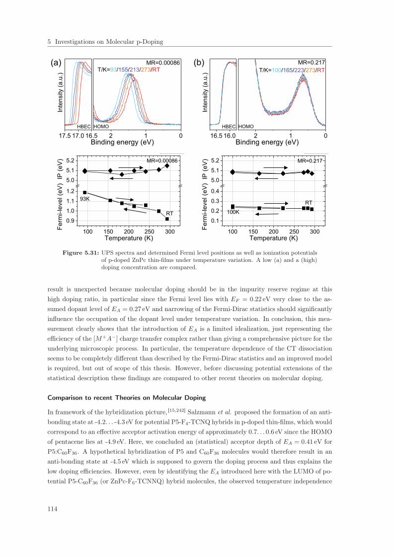
5 Investigations on Molecular p-Doping
Figure 5.31: UPS spectra and determined Fermi level positions as well as ionization potentialsof p-doped ZnPc thin-films under temperature variation. A low (a) and a (high)doping concentration are compared.
result is unexpected because molecular doping should be in the impurity reserve regime at thishigh doping ratio, in particular since the Fermi level lies with EF = 0.22 eV very close to the as-sumed dopant level of EA = 0.27 eV and narrowing of the Fermi-Dirac statistics should significantlyinfluence the occupation of the dopant level under temperature variation. In conclusion, this mea-surement clearly shows that the introduction of EA is a limited idealization, just representing theefficiency of the [M+A−] charge transfer complex rather than giving a comprehensive picture for theunderlying microscopic process. In particular, the temperature dependence of the CT dissociationseems to be completely different than described by the Fermi-Dirac statistics and an improved modelis required, but out of scope of this thesis. However, before discussing potential extensions of thestatistical description these findings are compared to other recent theories on molecular doping.
Comparison to recent Theories on Molecular Doping
In framework of the hybridization picture, [15,242] Salzmann et al. proposed the formation of an anti-bonding state at -4.2. . . -4.3 eV for potential P5-F4-TCNQ hybrids in p-doped thin-films, which wouldcorrespond to an effective acceptor activation energy of approximately 0.7. . . 0.6 eV since the HOMOof pentacene lies at -4.9 eV. Here, we concluded an (statistical) acceptor depth of EA = 0.41 eV forP5:C60F36. A hypothetical hybridization of P5 and C60F36 molecules would therefore result in ananti-bonding state at -4.5 eV which is supposed to govern the doping process and thus explains thelow doping efficiencies. However, even by identifying the EA introduced here with the LUMO of po-tential P5-C60F36 (or ZnPc-F6-TCNNQ) hybrid molecules, the observed temperature independence
114
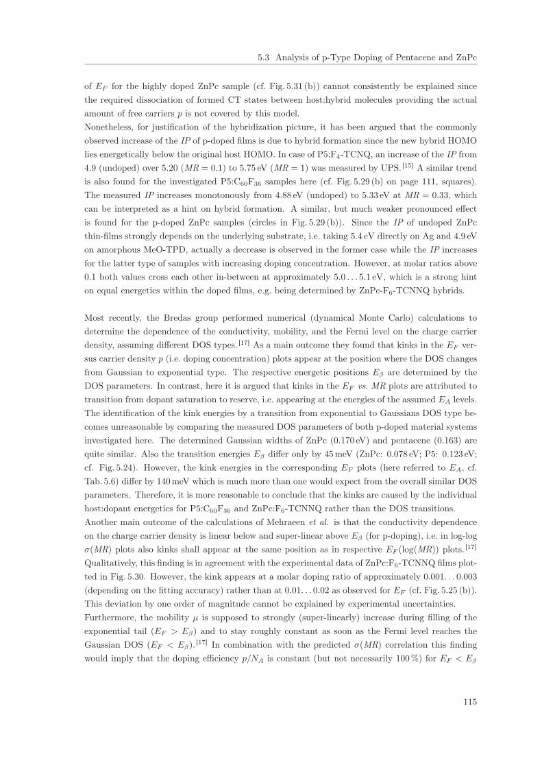
5.3 Analysis of p-Type Doping of Pentacene and ZnPc
of EF for the highly doped ZnPc sample (cf. Fig. 5.31 (b)) cannot consistently be explained sincethe required dissociation of formed CT states between host:hybrid molecules providing the actualamount of free carriers p is not covered by this model.Nonetheless, for justification of the hybridization picture, it has been argued that the commonlyobserved increase of the IP of p-doped films is due to hybrid formation since the new hybrid HOMOlies energetically below the original host HOMO. In case of P5:F4-TCNQ, an increase of the IP from4.9 (undoped) over 5.20 (MR = 0.1) to 5.75 eV (MR = 1) was measured by UPS. [15] A similar trendis also found for the investigated P5:C60F36 samples here (cf. Fig. 5.29 (b) on page 111, squares).The measured IP increases monotonously from 4.88 eV (undoped) to 5.33 eV at MR = 0.33, whichcan be interpreted as a hint on hybrid formation. A similar, but much weaker pronounced effectis found for the p-doped ZnPc samples (circles in Fig. 5.29 (b)). Since the IP of undoped ZnPcthin-films strongly depends on the underlying substrate, i.e. taking 5.4 eV directly on Ag and 4.9 eVon amorphous MeO-TPD, actually a decrease is observed in the former case while the IP increasesfor the latter type of samples with increasing doping concentration. However, at molar ratios above0.1 both values cross each other in-between at approximately 5.0 . . . 5.1 eV, which is a strong hinton equal energetics within the doped films, e.g. being determined by ZnPc-F6-TCNNQ hybrids.
Most recently, the Bredas group performed numerical (dynamical Monte Carlo) calculations todetermine the dependence of the conductivity, mobility, and the Fermi level on the charge carrierdensity, assuming different DOS types. [17] As a main outcome they found that kinks in the EF ver-sus carrier density p (i.e. doping concentration) plots appear at the position where the DOS changesfrom Gaussian to exponential type. The respective energetic positions Eβ are determined by theDOS parameters. In contrast, here it is argued that kinks in the EF vs. MR plots are attributed totransition from dopant saturation to reserve, i.e. appearing at the energies of the assumed EA levels.The identification of the kink energies by a transition from exponential to Gaussians DOS type be-comes unreasonable by comparing the measured DOS parameters of both p-doped material systemsinvestigated here. The determined Gaussian widths of ZnPc (0.170 eV) and pentacene (0.163) arequite similar. Also the transition energies Eβ differ only by 45 meV (ZnPc: 0.078 eV; P5: 0.123 eV;cf. Fig. 5.24). However, the kink energies in the corresponding EF plots (here referred to EA, cf.Tab. 5.6) differ by 140 meV which is much more than one would expect from the overall similar DOSparameters. Therefore, it is more reasonable to conclude that the kinks are caused by the individualhost:dopant energetics for P5:C60F36 and ZnPc:F6-TCNNQ rather than the DOS transitions.Another main outcome of the calculations of Mehraeen et al. is that the conductivity dependenceon the charge carrier density is linear below and super-linear above Eβ (for p-doping), i.e. in log-logσ(MR) plots also kinks shall appear at the same position as in respective EF (log(MR)) plots. [17]
Qualitatively, this finding is in agreement with the experimental data of ZnPc:F6-TCNNQ films plot-ted in Fig. 5.30. However, the kink appears at a molar doping ratio of approximately 0.001. . . 0.003(depending on the fitting accuracy) rather than at 0.01. . . 0.02 as observed for EF (cf. Fig. 5.25 (b)).This deviation by one order of magnitude cannot be explained by experimental uncertainties.Furthermore, the mobility μ is supposed to strongly (super-linearly) increase during filling of theexponential tail (EF > Eβ) and to stay roughly constant as soon as the Fermi level reaches theGaussian DOS (EF < Eβ). [17] In combination with the predicted σ(MR) correlation this findingwould imply that the doping efficiency p/NA is constant (but not necessarily 100 %) for EF < Eβ
115

5 Investigations on Molecular p-Doping
(i.e. EF < EA), which is in clear contradiction to the measurement results presented in this thesis. Incontrast, the observed decreasing doping efficiency in the dopant reserve regime would correspondto a sub-linear p vs. MR correlation (cf. Fig. 5.12 (b) on page 86 (b)). For lower concentrations(impurity saturation, EF > EA), direct proportionality would be expected: p ∝ MR. However,since the concentration dependence of the mobility μ(MR) cannot be independently measured, theactual p ∝ (MR)n correlation is not unambiguously determinable from σ(MR) experimental data,which prevents a verification of either Fig. 5.12 or the predications of Mehraeen et al.. Interest-ingly, for larger Gaussian DOS widths, e.g. of 4.5 kBT ≈ 120meV, Mehraeen et al. calculated astrongly increasing mobility by one order of magnitude per decade of doping concentration, evenfor EF < Eβ . Such a behavior might overcompensate the decreasing doping efficiency upon dopantreserve which could finally lead to an approximately linear (or even super-linear) conductivity vs.doping concentration characteristics. The critical parameters, which control this correlation, arethe width of the Gaussian DOS as well as the real dopant activation energy ΔEA. In particular theinfluence of the latter has been neglected by Mehraeen et al., i.e. σ, EF , and μ are calculated in de-pendence of the charge carrier concentration rather than the doping concentration. For comparisonto experimental data of n-doped C60 published by Olthof et al., [140] a constant doping efficiencyof 100 % was assumed but not verified by respective measurements. Nevertheless, good agreementbetween experiment and theory could be obtained, even under temperature variation.7 This resultis remarkable, since the used dopant molecules are very large and an additional reduction of themobility at higher doping concentrations upon disorder can be expected but is not considered inthe calculations. However, a comparison to other material systems remains open and at the currentstage of knowledge it is not clearly distinguishable wether the conclusions of Mehraeen et al. or ofthis thesis are closer to reality.
Outlook: Extension of the Statistical Description
Due to the discrepancies described above, it is necessary to improve the simple statistical descrip-tion aiming the development of a more comprehensive model on molecular doping. Possible newapproaches will be discussed in the following.The conducted calculations of the Fermi level and the doping efficiency are only based on the as-sumption of validity of the Fermi-Dirac statistics as well as the solution of the corresponding steadystate neutrality equation (cf. Sec. 5.2). The weak point of this approach is that all states of the as-sumed DOS are treated as equally mobile states, i.e. the effective mobility of all these states is equal.However, due to the hopping nature of transport in organic semiconductors, the mobility is actuallya function of energy μ(E). This is easy to understand, because the hopping probability decreasesexponentially with the energy difference of the initial and final state, i.e. jumps to energeticallymatched states are preferred. Since the density of states of similar energy within the exponentialtail is reduced by two orders of magnitude compared to the molecule density (cf. Fig. 5.24), theabsolute number of available jump partners is significantly reduced for a charge carrier occupyinga tail state. This means that even if the tail is filled by doping, the charge carriers are more orless trapped in these states. Hence, the steady state ratio p/NA, calculated as presented above,must inherently overestimate the real doping efficiency, in particular at doping concentrations being
72.5 kBT and 5 kBT were used as Gaussian and exponential DOS widths in the calculations.
116

5.3 Analysis of p-Type Doping of Pentacene and ZnPc
similar to the density of tail states, i.e. typically at molar ratios below 10−2 . . . 10−3. This effectcauses therefore the deviation between experiment and theory for the doping efficiency in ZnPc:F6-TCNNQ (cf. Fig 5.27 (b)).To overcome this circumstance, two approaches for extension of the model are conceivable. On theone hand, an appropriate dimensionless mobility function μ(E) could be introduced and the densityof free carriers calculated by a respective convolution of the usual Fermi-integral with μ(E):
p =
∫dE g(E)μ(E) [1− f(E,EF )] . (5.30)
Here, the unknown function μ(E) has to be quantified. In a first step, a mobility edge Eμ could bedefined, which means in case of p-doping the calculation of p by Eq. (5.30) and setting
μ(E) =
⎧⎨⎩0 , E > Eμ
1 , E < Eμ
. (5.31)
For smoothing the sharpness of the mobility edge, an ansatz equal to the Fermi-Dirac statisticsmight be possible:
μ(E) =1
1 + exp[E−Eμ
βμ
] . (5.32)
Here, βμ is a parameter which plays the role of kBT in the Fermi-Dirac statistics, i.e. it defines theextension in energy over which μ(E) switches from 0 to 1. Eμ sets the position of the mobility edgewithin the DOS. For instance, it is reasonable to identify Eμ with the transition energy betweenGaussian and exponential tail states (Eβ in Fig. 5.24), which reflects the assumption that tail stateshave trap character. Alternatively, the mobility edge could also be set to an appropriate positionin the low energy part of the Gaussian, which would correspond to a kind of transport edge ortransport energy as commonly assumed in framework of hopping transport models. [302,303] It hasalso been suggested to calculate the hopping mobility in a Gaussian DOS from the differential formof the generalized Einstein relation which yields [310]
μ(E) ∝ λ2(E)νesc(E)
kBT[1 + exp
(EF−EkBT
)] . (5.33)
Here, λ(E) is the mean hopping jump distance and νesc(E) the total escape rate. However, theseparameters as well as an additional proportionally factor are still unknown, but can be obtainedby fitting to experimental data. A comparison to conductivity measurements on p-doped ZnPcof Maennig et al. [180] yields νesc = 1012 s−1. Furthermore, the presence of deep hole traps withET = 1 eV and NT = 9.5×1017 cm−3 was deduced from this model, which is in very good agreementto the values given in Tab. 5.6. Finally, the preferred solution would be the determination of anexact mobility function μ(E), reflecting the hopping properties of each individual state of the DOSin dependence of occupation of its neighboring sites considering also morphological aspects likemolecular packing and resulting inter-molecular distances.In a second approach to extend the molecular doping model, actual dynamic calculations of hoppingin interplay with dopant activation could be performed, e.g. by kinetic Monte Carlo simulations.
117

5 Investigations on Molecular p-Doping
The main issue here is to combine this kind of description with the concept of Fermi level and/ordopant levels EA or ED. In particular the applicability of the Fermi-Dirac statistics to so-called freecarriers, which are moving via hopping transport, must be clarified. This task is not trivial, since thehopping rate of a charge carrier at higher energy levels might be independent of a carrier which jumpsat lower energies. This circumstance is due to the fact that the jump probability νij does dependon the energetic difference between initial and final Ei − Ej state rather then on their (average)absolute values. This dependence appears only indirectly due to the non-uniformity of the density ofstates as explained above. In contrast, Fermi-Dirac statistics considers all carriers indistinguishable(equally) mobile which are above or close the Fermi level which defines the occupation boundary.Furthermore, the presence and clear definition of trap states must be included in an extended model.Here, the main issue is to find characteristic trapping times (recombination rates) rather then justtrap depths for describing their occupation with charge carriers.Finally, the dopant activation process must be implemented, i.e. a physical motivation or substitutionfor the introduced levels EA has to be found. In particular the relative energy level alignmentbetween diluted dopant molecules in a surrounding of host molecules as well as the process of[M+A−] dissociation must be studied in a microscopic model.
5.4 Summary
Molecular p-doping has been studied by UPS and impedance spectroscopy for various thermally co-evaporated thin-films. In particular the Fermi level shift upon variation of the doping concentrationsas well as the doping efficiency has been measured. The experimental results for three host materialsdoped by different p-dopant molecules are compared to a statistical description. Dopant reserve,as known from the classical semiconductor physics, could be confirmed for all investigated materialcombinations. Furthermore, it was shown that deep trap states with densities in the range ofMR = 4× 10⁻⁵ (pentacene), 5× 10⁻⁴ (ZnPc), and 2× 10⁻³ (MeO-TPD) are hindering the dopingprocess at very low concentrations. Additionally, it could quantitatively be verified for MeO-TPDthin-films that the absolute density as well as the energy distribution of the traps correlate withthe material purity. Finally, three characteristic regimes are identified by varying the molar dopingratio over five orders of magnitude for p-doped pentacene and ZnPc films: Trap-filling, dopantsaturation, and reserve. The transitions between these regions are characterized by respective kinksin the Fermi level vs. molar doping ratio plots. In particular the transition between the dopantsaturation and reserve regimes could be modeled by the introduction of appropriate acceptor levelsEA which pinn the Fermi level at high doping concentrations and therefore cause the low observeddoping efficiencies.In contrast, kinks in measured Fermi level vs. molar doping ratio plots have been explained inliterature by a transition of the Fermi level from exponential tail (trap) states to the GaussianDOS at the example of n-doped thin-films. [17,140] Furthermore, low doping efficiencies in molecularp-doped systems were independently attributed to the formation of dopant-host hybrid moleculeswith a LUMO lying several 100 meV above the host HOMO. [15] This energetic distance is supposedto equal the activation energy of the molecular doping process. In comparison, the statisticaldescription presented here is able to explain both effects by introduction of the effective acceptorlevel EA.
118

6 | Investigations on Molecular n-Doping
In this chapter, UPS investigations on molecular n-doping with the strong donor ma-terial W2(hpp)4 are presented. First, the Fermi level positions versus the dopingconcentrations are shown for three different host materials. Applying the statisticaldoping model presented in the previous chapter allows for determination of electrontrap densities and an estimation of the doping efficiency in these materials. In thesecond section, the interesting passivation effect of W2(hpp)4 contained in n-dopedlayers against degradation in air is studied by conductivity and UPS/XPS measure-ments. These studies particularly allow for new conclusions on the doping mechanismin general, which will finally be discussed in detail.
6.1 N-Type Doping by the Molecular Di-Metal Complex
W2(hpp)4
A thin-film of the di-metal complex W2(hpp)4 possesses a very small IP of only 2.4 eV, which makesthis material suitable as n-dopant for nearly all electron transport materials commonly applied inOLEDs, OPV, and transistor structures although being unstable in air. [198,201] Hence, the n-dopingeffect of W2(hpp)4 in pentacene and ZnPc is studied by UPS and compared to the conclusions drawnfrom respective p-doping experiments described in Sec. 5.3. Furthermore, n-doped C60 thin-filmsare investigated and compared to a recently published UPS study using [RuCp ∗ (mes)]2 dimers asn-dopants in C60. [140] Finally, the appearance of gap states in all investigated n-doped thin-films isdiscussed.
6.1.1 IPES on Pentacene, ZnPc, and C60 Thin-Films: Gap Determination
The exact LUMO positions or thin-film EAs of the host materials pentacene, ZnPc, and C60 arerequired for a quantitative analysis of the n-doping effect by W2(hpp)4. The commonly used es-timation IP + optical gap is not accurate enough for this purpose since it includes the unknownexciton binding energy which usually takes values of several 100 meV. Thus, the actual electronicgaps are needed but are not accessible by UPS. However, combined UPS and inverse photoemis-sion spectroscopy (IPES) measurements were conducted by Selina Olthof at Princeton University.Although the material batches (suppliers) are different from those used at the IAPP, the measuredEAs are assumed to be accurate insofar as the corresponding IPs are similar to values obtained byUPS at the IAPP.
119

6 Investigations on Molecular n-Doping
Figure 6.1: UPS/IPES spectra of the host materials pentacene, ZnPc, and C60, measured bySelina Olthof at Princeton University. The HOMO (LUMO) onsets are indicatedby circles (diamonds), whereas the respective peak positions are marked by dashes.All characteristic values are summarized in Tab. 6.1.
The combined UPS/IPES spectra obtained at Princeton are shown in Fig. 6.1 and the determinedenergy levels are summarized in Tab. 6.1. In comparison to UPS measurements at the IAPP, theobtained IPs at Princeton deviate by max. 50meV, i.e. by the same order as the experimental er-ror of UPS. The values are (IAPP/Princeton): 4.88 eV/4.88 eV (P5), 4.90 eV/4.85 eV (ZnPc), and6.48 eV/6.51 eV (C60). Similar deviations can therefore be expected for the EA values, i.e. the un-certainties in the corresponding electronic HOMO-onset to LUMO-onset gaps due to different usedmaterial batches are in the order of 100 meV, which is small enough for a reasonable quantitativeanalysis of the n-doping studies at the IAPP using only UPS.The widths of the HOMO-peaks measured by UPS either at the IAPP or in Princeton are also similar.For instance, this can be quantified by the energetic difference between the HOMO-peak positionsand respective HOMO-onsets, yielding (IAPP/Princeton): 0.48 eV/0.47 eV (P5), 0.33 eV/0.55 eV(ZnPc), and 0.48 eV/0.49 eV (C60). The values are practically equal except for ZnPc, where a muchbroader HOMO DOS is measured in Princeton. This deviation of 0.22 eV might be caused by thedifferent thin-film growth of ZnPc, which strongly depends on the used substrate and cannot beavoided. This finding is important since the exact energetic difference between the HOMO-peakand the LUMO-onset (EHpLo in Tab. 6.1) is required for systematic n-doping investigations. Therethe Fermi level is measured with respect to the HOMO-peak, but its distance to the LUMO-onset
host HBEC Wf HOMO LUMO gap IP EA EHpLopeak onset onset peak onsets peaksP5 18.42 2.80 2.55 2.08 -0.22 -1.02 2.30 3.57 4.88 2.58 2.77
ZnPc 17.22 4.00 1.40 0.85 -0.56 -1.60 1.41 3.00 4.85 3.44 1.96C60 16.93 4.29 2.71 2.22 -0.06 -0.83 2.28 3.54 6.51 4.23 2.77
Table 6.1: Energy levels and electronic gaps of pentacene, ZnPc, and C60 measured byUPS/IPES by Selina Olthof at Princeton University. EHpLo is the energetic dif-ference between the HOMO-peak and the LUMO-onset.
120

6.1 N-Type Doping by the Molecular Di-Metal Complex W2(hpp)4
is important from a theoretical standpoint of view. Thus, before drawing quantitative conclusionson the doping process from measured EF (MR) plots at the IAPP, it must be declared which elec-tronic gap measured at Princeton, i.e. whether the HOMO-peak to LUMO-onset or HOMO-onsetto LUMO-onset gap, will be applied to the UPS spectra obtained at the IAPP. Since energeticbroadening does not affect the HOMO-peak position, the HOMO-peak to LUMO-onset distance isassumed to be the more reliable gap. Consequently, the HOMO-onset to LUMO-onset gap of evapo-rated ZnPc films at the IAPP is assumed to be increased from the 1.41 eV measured in Princeton by0.22 eV (broadening) to 1.63 eV. This assumption is supported by an optical gap of 1.548 eV (801 nm)determined from absorption measurements at the IAPP1. A HOMO-onset to LUMO-onset gap ofjust 1.41 eV would not fit to this finding since the optical gap must be smaller than the electronicgap due to the exciton binding energy.
6.1.2 Fermi Level Shift in Pentacene, ZnPc, and C60 Thin-Films
The n-doping effect of W2(hpp)4 in pentacene, ZnPc, and C60 thin-films is investigated by UPSunder systematic variation of the doping concentration. In contrast to the p-doping studies, theposition of the Fermi level is here determined with respect to the HOMO-peak rather than theHOMO-onset since at higher doping concentrations, gap states appear which superimpose the lowbinding energy flank of the HOMO DOS and thus prevent the clear onset determination. The UPSspectra of n-doped pentacene and ZnPc thin-films are plotted in Fig. 6.2 where the host HOMO-peak positions are marked by circles (EF = 0). The investigated sample structures are Ag/MeO-TPD(4 nm)/n-P5(35 . . . 50 nm) and Ag/n-ZnPc(8 . . . 25 nm). The MeO-TPD layer is used to controlthe morphology of the P5 film (cf. Sec. 5.3.1). With increasing doping concentration, a clear shiftof the spectra towards higher binding energies is found for both material systems. Above molardoping ratios of approximately 0.01, gap states appear which finally dominate the spectral shapeof thin-films at doping ratios higher than 0.1. Interestingly, the energetic width of the gap statesin n-P5 is twice as high as in n-ZnPc. The gap states extend across the whole energy gap of thehost material, which is larger for pentacene (2.30 eV) than for ZnPc (1.41 eV), up to the Fermi level.Thus, an unambiguous determination of host HOMO-peak positions is hindered at the highest dop-ing concentrations, e.g. for the MR = 0.66 p-ZnPc sample (cf. Fig. 6.2 (b)).The obtained Fermi level positions with respect to the HOMO-peak positions are plotted in Fig. 6.3versus the molar doping ratio (filled symbols). Additionally, the HOMO and LUMO-onsets deter-mined by UPS/IPES (cf. Sec. 6.1.1) as well as the data points of corresponding p-doping studies(empty symbols) are shown. For both material systems, EF shifts much closer to the LUMO-onsetupon n-doping as observed towards the HOMO-onset for p-doping. Moreover, it even crosses theLUMO-onset at medium (n-ZnPc) or high (n-P5) doping ratios, whereas it is pinned several 100meVabove the HOMO-onset in case of p-doping. This result is remarkable since it suggests that n-dopingis much more efficient and not limited by a donor level ED deep in the tail of the LUMO DOS. Theshape of the EF vs. log(MR) plots supports this hypothesis. In particular for n-P5, a continuouslyincreasing relation without any kinks is observed for the investigated molar doping ratios between6.7× 10−4 and 0.66.In comparison to the basic calculations discussed in Fig. 5.11, these findings mean that the Fermi level1Absorption measurements are performed by Christiane Falkenberg at the IAPP. The optical gap is defined as the
low energy absorption onset.
121
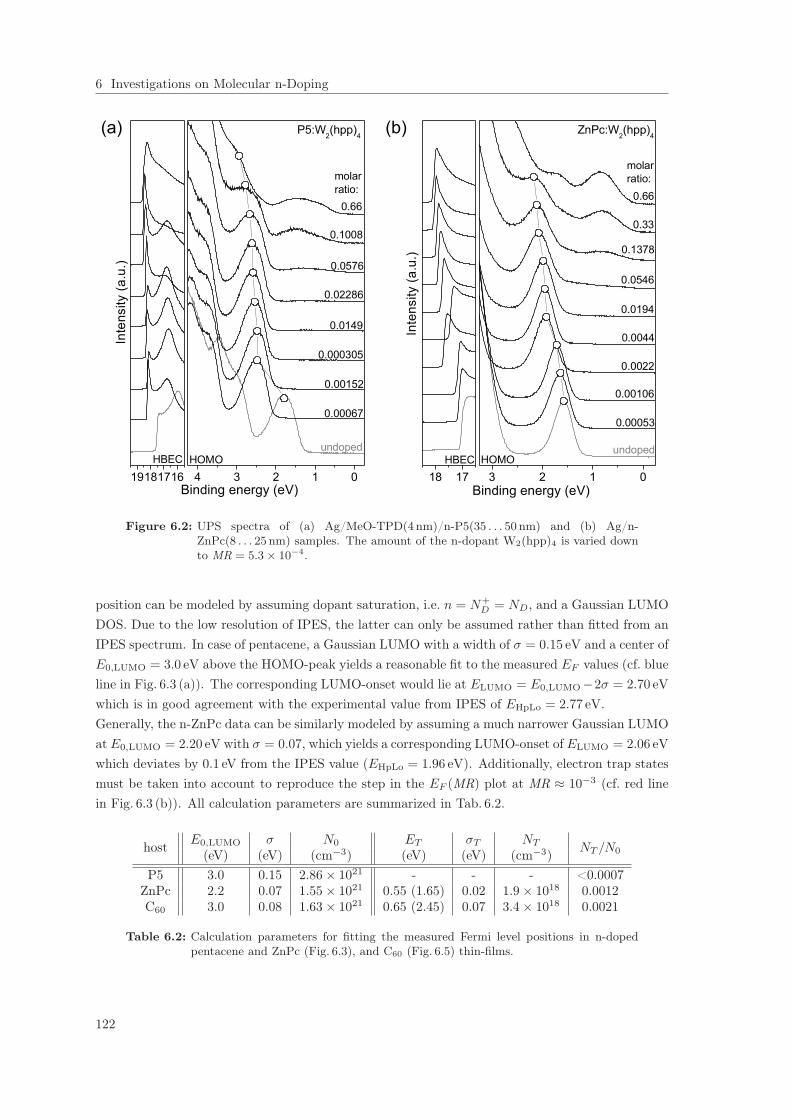
6 Investigations on Molecular n-Doping
Figure 6.2: UPS spectra of (a) Ag/MeO-TPD(4 nm)/n-P5(35 . . . 50 nm) and (b) Ag/n-ZnPc(8 . . . 25 nm) samples. The amount of the n-dopant W2(hpp)4 is varied downto MR = 5.3× 10⁻⁴.
position can be modeled by assuming dopant saturation, i.e. n = N+D = ND, and a Gaussian LUMO
DOS. Due to the low resolution of IPES, the latter can only be assumed rather than fitted from anIPES spectrum. In case of pentacene, a Gaussian LUMO with a width of σ = 0.15 eV and a center ofE0,LUMO = 3.0 eV above the HOMO-peak yields a reasonable fit to the measured EF values (cf. blueline in Fig. 6.3 (a)). The corresponding LUMO-onset would lie at ELUMO = E0,LUMO−2σ = 2.70 eV
which is in good agreement with the experimental value from IPES of EHpLo = 2.77 eV.Generally, the n-ZnPc data can be similarly modeled by assuming a much narrower Gaussian LUMOat E0,LUMO = 2.20 eV with σ = 0.07, which yields a corresponding LUMO-onset of ELUMO = 2.06 eV
which deviates by 0.1 eV from the IPES value (EHpLo = 1.96 eV). Additionally, electron trap statesmust be taken into account to reproduce the step in the EF (MR) plot at MR ≈ 10−3 (cf. red linein Fig. 6.3 (b)). All calculation parameters are summarized in Tab. 6.2.
host E0,LUMO σ N0 ET σT NT NT /N0(eV) (eV) (cm−3) (eV) (eV) (cm−3)P5 3.0 0.15 2.86× 10²¹ - - - <0.0007
ZnPc 2.2 0.07 1.55× 10²¹ 0.55 (1.65) 0.02 1.9× 10¹⁸ 0.0012C60 3.0 0.08 1.63× 10²¹ 0.65 (2.45) 0.07 3.4× 10¹⁸ 0.0021
Table 6.2: Calculation parameters for fitting the measured Fermi level positions in n-dopedpentacene and ZnPc (Fig. 6.3), and C60 (Fig. 6.5) thin-films.
122

6.1 N-Type Doping by the Molecular Di-Metal Complex W2(hpp)4
Figure 6.3: Fermi level positions of pentacene (a) and ZnPc (b) thin-films n-doped by W2(hpp)4(closed symbols). EF = 0 refers to the HOMO-peak positions. For comparison,UPS data of P5:C60F36 and ZnPc:F6-TCNNQ (open symbols) as well as the HOMOand LUMO-onset positions determined by IPES are given. The solid lines indicatecalculated curves assuming Gaussian LUMO DOS and dopant saturation. Respec-tive LUMO and additional trap parameters are summarized in Tab. 6.2.
Since the Fermi level curve of n-P5 does not show any kink above MR = 6.7 × 10⁻⁴, trap statesof higher concentration are not expected, but could be present with lower density. However,since the LUMO level of C60 lies below that of pentacene by approximately 1.6 eV (cf. Fig. 6.4),it should be possible to intentionally introduce deep electron traps by co-evaporation of P5 andC60. These traps can purposefully be filled by n-doping the P5:C60 blend with W2(hpp)4. To val-idate this hypothesis, two UPS samples with P5:C60:W2(hpp)4 thin-films are compared: One withMR(W2(hpp)4)< MR(C60) and the other vice versa. For both samples, the C60 concentration isfixed to MR � 0.03, whereas the W2(hpp)4 concentrations are MR = 0.003 and MR = 0.1 which aresimilar to samples without C60. The two determined Fermi level positions are shown in Fig. 6.3 (a)by black diamond symbols. In case of MR = 0.1, the Fermi level lies at 2.74 eV which is close tothe position without C60 (EF = 2.78 eV). For the MR = 0.003 sample, EF is shifted only to 1.9 eV,i.e. just above the undoped position, whereas EF = 2.56 eV was found for an usual P5:W2(hpp)4thin-film. This result clearly confirms that C60 molecules really act as electron traps in pentacene,which control the Fermi level position at low doping concentrations. As soon as the dopant densityof W2(hpp)4 exceeds the C60 density, all these traps are filled and the Fermi level shifts stronglytowards the pentacene LUMO. The position of this strong shift is supposed to be tunable by theC60 concentration. However, besides this special material combination, the above finding is also ofgeneral importance since it gives experimental evidence for the assumptions of the statistical dopingmodel, i.e. the presence of deep trap states which control doping at low concentrations, and itsconclusions on the mechanism of molecular doping.Finally, n-doping of C60 thin-films by W2(hpp)4 co-evaporated on Au-foil is studied by UPS. Cor-responding spectra are plotted in Fig. 6.5 (a) and the Fermi level positions with respect to the C60
123

6 Investigations on Molecular n-Doping
Figure 6.4: Energy levels of W2(hpp)4 (gray), pentacene (blue), and C60 (black). Electrontransfer to the pentacene LUMO provides n-doping. However, C60 molecules co-evaporated in pentacene thin-films are supposed to form electron traps with a depthof approximately 1.6 eV.
HOMO-peak position are summarized in Fig. 6.5 (b). Below a molar doping ratio of approximately2× 10−3, a stronger drop of the Fermi level into the gap is observed which indicates the presence oftraps also here. Qualitatively, the data of Fig. 6.5 are in agreement with recent UPS measurementsof Olthof et al. on C60 thin-films doped by [RuCp*(mes)]2 dimers where a similar kink was foundat MR � 4× 10⁻³. [140] There, it was argued that the transition from exponential tail (trap) statesto the Gaussian LUMO density causes this kink. Here, it shall be argued similarly, but slightlydifferent. The kink is supposed to be caused by deeper electron traps of Gaussian type with a den-sity of 3.4× 1018 cm−3 (NT /N0 = 2× 10⁻³) and a depth of 0.65 eV. The Fermi level curve is againcalculated by the statistical approach assuming dopant saturation, i.e. solving n+N−
T = N+D = ND
with a Gaussian LUMO at E0,LUMO = 3.0 eV and a width of 80meV, i.e a LUMO-onset at 2.84 eVwhich is close the experimental IPES value of EHpLo = 2.77 eV (cf. Sec. 6.1.1). The HOMO andLUMO-onsets determined by UPS/IPES are indicated by gray lines in Fig. 6.5 (b). Here, EF shiftsacross the LUMO-onset at a medium concentration of MR ≈ 10−2 as well. The calculation param-eters are summarized in Tab. 6.2. Very good agreement to the experimental values is achieved forall investigated doping concentrations. In particular the kink as well as the positions of the twoweak doped samples are reproduced more accurately than suggested by fitting with a straight linein Ref. [140]. However, as extensively discussed in framework of determination of hole-trap distribu-tions in different purification grades of MeO-TPD (cf. Sec. 5.2.4), the deduced trap depth can onlybe regarded as estimation due to the substrate dependence of the Fermi level position for undopedorganics on metals. The same argumentation holds true here.
124

6.2 Self-Passivation of Molecular n-Type Doping
Figure 6.5: (a) UPS spectra of Au/n-C60 (6 . . . 25 nm) samples. The amount of the n-dopantW2(hpp)4 is varied down to MR = 6.7 × 10⁻⁴. (b) Corresponding Fermi levelpositions with respect to the C60 HOMO-peak. The black line has been calculatedby the statistical model.
6.2 Self-Passivation of Molecular n-Type Doping
The degradation of W2(hpp)4 molecules in pure films as well as doped into various host materialsis systematically investigated under air exposure by conductivity, UPS/XPS, and LDI-TOF-MSmeasurements. In particular, a passivation of the n-doping effect in n-doped C60 and Bis-HFl-NTCDIis observed whereas it completely vanishes in pentacene and ZnPc thin-films after air exposure.Based on these findings, conclusions on the physical mechanism of molecular n-doping, in particularon the relative host:dopant energy level alignment, are discussed in Sec. 6.3.
6.2.1 Passivation of W2(hpp)4 in C60
First, the stability of C60:W2(hpp)4 thin-films under air exposure is analyzed since this materialcombination is important for novel vertical transistor concepts with high performance. [278,279] Inparticular, state of the art devices are structured by photo-lithography which is commonly performedunder ambient (clean-room) conditions. [237] Therefore, the application of the W2(hpp)4 n-dopantcompound was supposed to be unsuitable in these devices due to its air-sensitivity. However, incontrast to this expectation, it will be shown that the n-doping effect in C60 thin-films is partiallypassivated against degradation in air, at least in a time frame of a few minutes. Surprisingly, similarfindings are obtained for pure W2(hpp)4 thin-films evaporated on Au or SiO2 surfaces.
125

6 Investigations on Molecular n-Doping
Conductivity and Seebeck Measurements
First, a C60:W2(hpp)4 (30 nm, 4 wt%) thin-film is prepared and investigated in situ.2 The conduc-tivity of the fresh film in vacuum is measured to 1.88 S/cm after thermal annealing at 120◦C for 1hour and subsequent re-cooling to 25◦C. Next, the sample is removed from vacuum and exposed toair for 16 minutes, continuously probing the conductivity which is plotted in Fig. 6.6 (a). An imme-diate drop by 5 orders of magnitude down to a value of 1.7× 10⁻⁵ S/cm is observed. Directly after,the measurement chamber with the sample is evacuated again. Upon evacuation the conductivityincreases to 2.1×10⁻³ S/cm at a pressure of 2×10⁻⁷ mbar which is reached after approximately 10 h(cf. Fig. 6.6 (b)). Hence, 0.1 % of the initial conductivity is restored, indicating that the molecularn-doping is still intact. By slowly heating the sample up to 120◦C, the conductivity is restored evenfurther and saturates after cooling down to room temperature at 0.60 S/cm which is 1/3 of its initialvalue.Extending the air exposure time to 3 hours yields a further conductivity drop to 6.6 × 10⁻⁷ S/cm.Re-evacuating the vacuum chamber recovers the conductivity to 2.3× 10⁻⁵ S/cm and a subsequentheat treatment to 0.03 S/cm. Hence, the much longer air exposure reduces the final conductivityby factor of approximately 60 compared to the initial value of 1.88 S/cm. However, it is still closeto the conductivity of a freshly fabricated and annealed C60 layer doped by the air-stable precursorcompound acridine orange base (AOB). [230]
Similar conductivity drops have been reported in literature for metal doped C60 and were attributedto the formation of deep oxygen related electron traps, [311] which are further correlated to the for-mation of fullerene ferites by O2 bridges. [312] Besides, the charge carrier mobility in C60 is supposedto suffer from air exposure by several orders of magnitude. [313] However, thermal annealing of re-
σ
σ
σ
Figure 6.6: Conductivity measurements on a 30 nm C60 thin-film n-doped by 4 wt% W2(hpp)4:During air exposure (a) and after re-evacuation and thermal annealing (b). Themeasurements are performed by Torben Menke.
2The measurements are performed by Torben Menke with the Seebeck setup of the IAPP. Experimental details canbe found in Ref. [231]
126

6.2 Self-Passivation of Molecular n-Type Doping
spective oxygen and hydrogen related electron traps in C60 has been measured directly by thethermally stimulated current technique and validated by enhanced OFET mobilities of 4 orders ofmagnitude. [314] Therefore, the decrease in conductivity and subsequent restoration observed here donot necessarily mean that the n-doping is destroyed by a degradation of W2(hpp)4 due to oxidationin air. Instead, we conclude that the n-doping is at least partially intact during air exposure andonly compensated by oxygen related traps and/or p-doping effects.
Before and after each air exposure Seebeck measurements are performed. The Seebeck coefficient Sat a mean temperature (Tm = 40◦C) is correlated to the energetic difference ES between the Fermilevel EF and an assumed (average) transport energy ETr via [310,315]
ES = ETr − EF = e ·Tm · |S| . (6.1)
It is thus a direct measure for the density of free electrons generated by molecular n-doping. Forthe 4wt% C60:W2(hpp)4 sample, ES is increased by 8.8meV to 82.3 meV upon 16 minutes of air ex-posure. The second exposure of 3 hours leads to an additional rise of ES by 28.0 meV to 110.3 meV,which generally corresponds to an increased difference between the Fermi level and the transportenergy and thus to less free electrons. However, the Seebeck energy ES of the 4wt% sample(MR = 0.033) after such a long air exposure is still lower than that of a freshly prepared sam-ple with a tenth of the doping concentration measured in situ: Here, ES = 167meV at 0.5 wt%(MR = 0.004). [201] This comparison clearly demonstrates that for the 4wt% sample, at least 10 %of the W2(hpp)4 molecules have to survive the degradation in air and still provide a significantn-doping effect in C60. Furthermore, the Seebeck coefficients S are negative, i.e. the n-doping isstronger than a possible p-doping of C60 by oxygen in air.
UPS: C60:W2(hpp)4 and W2(hpp)4 on Au
The results from Seebeck are confirmed by UPS which is illustrated in Fig. 6.7 (a). There, the UPSspectra of 12 nm intrinsic and 10 nm n-doped (10wt%, MR = 0.087) C60 thin-films evaporated on Auare compared. The Fermi level is shifted by 0.51 eV towards the C60 LUMO upon n-doping, yieldingEF = 2.82 eV with respect to the HOMO-peak position (cf. also Fig. 6.5). After exposing the dopedfilm for 1 minute to air, the Fermi level shifts only by 40 meV back into the gap (EF = 2.78 eV).Also the HBEC is increased from 4.07 eV to just 4.12 eV. These findings clearly show a conservationof the n-doping effect. However, gap states which arise due to n-type doping disappear after airexposure (cf. inset of Fig. 6.7 (a)), which is a hint that several of the W2(hpp)4 molecules are actuallydegrading in air. Nonetheless, a sufficiently large amount of dopant molecules is still intact becausethe Fermi level position as well as the HBEC are nearly unaffected by air. Heating the air exposedsample slowly to 110◦C for 54minutes yields a further weak shift of the UPS spectrum by 80meV toeven lower binding energies (EF = 2.70 eV), i.e. the density of free carriers is not increased. Hence,the above described increase in conductivity after heat treatment must be assigned to an annealingof trap states and hence of the mobility rather than to a chemical annealing of degraded W2(hpp)4molecules.In addition to the n-doped C60 films, the degradation of a 4 nm layer of pure dopant molecules onAu is investigated to check whether the protection of W2(hpp)4 against oxidation in air is assigned
127

6 Investigations on Molecular n-Doping
Figure 6.7: (a) UPS spectra of a 10 nm C60 thin-film n-doped by 10 wt% of W2(hpp)4: freshlyprepared (blue), exposed to air for 1 min (light green) and subsequently thermalannealed in UHV up to 110◦C for 54 min (dark green). As reference, a spectrumof 12 nm intrinsic C60 evaporated on gold is shown (dashed line). The inset showsan enlarged portion of the spectra with gap states up to the Fermi level arising dueto n-doping. (b) UPS spectra of a 4 nm W2(hpp)4 thin-film on gold-foil: freshlyprepared (blue), exposed to air for 1 min (light green), and thermally annealed inUHV afterwards up to 120◦C for 74 min (dark green). As reference, the spectrumof the gold substrate is shown (dashed line). The inset shows a magnification ofthe spectra close to the Fermi level.
to integration of W2(hpp)4 molecules into the C60 matrix or to a universal thin-film property.Respective UPS spectra are shown in Fig. 6.7 (b). For the freshly prepared W2(hpp)4 film, anIP = 2.40 eV is measured at a HOMO-onset of 0.29 eV below the Fermi level (Wf = 2.11 eV).Exposing the sample for 1 minute to air significantly shifts the HBEC to lower binding energies, whichincreases the thin-film work function to 3.09 eV. The density of occupied states in the HOMO regionis smeared out which indicates a damage of most of the W2(hpp)4 molecules, at least directly at thesurface. Heating the degraded film in ultra-high vacuum (UHV) stepwise to 50◦C (15 min), 80◦C(37 min), and 120◦C (74min) shifts the HBEC to even higher binding energies, which corresponds toa stepwise increase of the film work function to 3.47 eV, 3.74 eV, and 4.06 eV. Furthermore, featuresof the underlying gold substrate arise in the HOMO region with increasing temperature, showingfinally a clear Fermi edge (c.f. inset of Fig. 6.7 (b)). Since a weak Fermi edge is also visible in theair exposed film spectrum, it can be concluded that at least one of the degradation products seemsto be volatile in vacuum and can be further removed from the film by heating. In summary, thisexperiment shows that a pure film of W2(hpp)4 molecules is not stable in air, which is furtherconfirmed by respective XPS measurements.
128

6.2 Self-Passivation of Molecular n-Type Doping
Figure 6.8: C1s, Au4f, and O1s peaks of a pure 4 nm W2(hpp)4 (a) and a doped C60:W2(hpp)4(10 nm, 10 wt%) thin-film (b) each evaporated on Au. The peaks of the freshlyprepared samples, after 1 minute of exposure to air and of subsequent thermalannealing at 120◦C for 1h are plotted.
XPS: C60:W2(hpp)4 and W2(hpp)4 on Au
The C1s, Au4f, O1s (Fig. 6.8), N1s (Fig. 6.9), and W4f peaks (Fig. 6.10) are scanned by XPS forboth freshly prepared sample types, after exposure to air for 1minute, and after subsequent heattreatment. In case of the pure W2(hpp)4 film, the C1s peak strongly decreases after air exposureand heating, accompanied by an increase of the Au4f peak of the underneath gold substrate, whichindicates the (partial) volatility of the degradation products. Similar results are obtained for the10 wt% n-doped C60 film, but with relatively lower intensity decays. Furthermore, the detected
129

6 Investigations on Molecular n-Doping
amount of oxygen in the thin-films is strongly increased after air exposure and remains nearlyunchanged after the heating step, in particular for the pure W2(hpp)4 layer, indicating that theoxygen is bound to degradation products, e.g. by formation of WOx.Drastic changes in shape are observed for the N1s peaks (cf. Fig. 6.9). For the freshly preparedW2(hpp)4 film, N1s consists of two sub-peaks at 399.51 eV and 401.10 with a fixed relative intensityratio of 2:1 and L:G ratios3 of 40 %. The sub-peak with the higher intensity can be attributed tothe N-atoms which are involved in the bonding to the W2-core of a W2(hpp)4 molecule and thesecond peak to the N-atoms which are positioned at the outer ends of the (hpp) ”paddles”. Afterair exposure, a third undefined bonding state at EB = 400.57 eV with a relative intensity of 41.1 %appears (red sub-peak in Fig. 6.9 (a)). After thermal annealing, the shape of the original N1s peakis recovered, consisting of two sub-peaks with equal relative intensities and energetic splitting, butlower absolute intensity as N1s peak of the freshly prepared film. Hence, it can be concluded thatthe W2(hpp)4 molecules partially break at their W-N bonds as main degradation mechanism, i.e.the (hpp) ”paddles” are detached from the W2 core in air and react with oxygen and hydrogen tovarious degradation products. These different products are identified by LDI-TOF measurements(cf. Sec. 6.2.1). Since these species seem to be volatile under vacuum and furthermore removable bythermal annealing, the recovered N1s peak after heating mainly represents the remaining undamagedW2(hpp)4 molecules on the gold surface. Scanning the N1s peaks of the C60:W2(hpp)4 film yieldsgenerally the same results (cf. Fig. 6.9 (b)). However, the plain 2:1 N1s double peak of the freshlyprepared film cannot completely be recovered by annealing, i.e. respective degradations productsare more strongly trapped within the C60 film.The W4f core level peaks of the tungsten atoms are also analyzed in detail (cf. Fig. 6.10). For thepure dopant film, the W4f doublet is fitted by peaks at 35.17 eV (W4f5, L:G=58 %) and 33.03 eV(W4f7, L:G=53%) with fixed intensity ratio of 3:4. The W4f signal splits up into two doublets afterair exposure for 1minute. The major doublet is shifted by approximately 2.5 eV to higher bindingenergies, i.e. 37.68 eV (W4f5) and 35.54 (W4f7) (red doublet), whereas the minor doublet remainsnearly at the same position, 35.64 eV (W4f5) and 33.47 (W4f7) (blue doublet). Thus, the minordoublet can be interpreted as the fraction of undamaged W2(hpp)4 molecules (21.0 %) whereas themajor doublet (79.0%) as new bonding states of W (e.g. W2), hence representing the unknowndegradation products.4 In case of the n-doped C60 film, identical results are obtained, here therelative fractions of intact/degraded W2(hpp)4 molecules are 20.0 %/80.0 %. Heating the layersbrings these ratios more into line, i.e. yielding intact/degraded W2(hpp)4 amounts of 42.1 %/57.9%for the n-C60 and 26.6%/73.4 % for the pure dopant film. A removal of the W containing degradationproducts similar to the (hpp)4 fragments might be one reason for the (relatively) increased amountof the intact W4f doublets. However, a diffusion of degradation products as well as of completeW2(hpp)4 molecules, in particular in case of the doped film, might also be possible. This presumptionis supported by the fact that not only the undamaged/degraded ratio, but also the absolute W4fintensity of the intact W2(hpp)4 molecules increases after the heat treatment (cf. Fig. 6.10 (b)).Since XPS is most sensitive in the first nanometer beyond the film surface, these diffusion effectswould distort the XPS signal which hinders an unambiguously comparison to the freshly preparedfilm peaks. However, the topic of dopant diffusion in C60 will be addressed separately in Sec. 6.2.2.
3Details on the XPS peak fitting procedure are described in Sec. 4.3.3.4For both species, the L:G ratios, FWHMs, and relative intensities (3:4) are kept constant during the peak fitting.
130

6.2 Self-Passivation of Molecular n-Type Doping
Figure 6.9: N1s peaks of a pure 4 nm W2(hpp)4 (a) and a doped C60:W2(hpp)4 (10 nm, 10 wt%)thin-film (b) each evaporated on Au and measured by XPS as freshly prepared,after 1 minute of air exposure and after subsequent thermal annealing at 120◦C for1h. The blue (red) fitted sub-peaks are assigned to intact (degraded) W2(hpp)4molecules.
131

6 Investigations on Molecular n-Doping
Figure 6.10: W4f peaks of a pure 4 nm W2(hpp)4 (a) and a doped C60:W2(hpp)4(10 nm, 10 wt%) thin-film (b) each evaporated on Au and measured by XPS asfreshly prepared, after 1 minute of air exposure and after subsequent thermal an-nealing at 120◦C for 1h. The blue (red) fitted sub-peaks are assigned to intact(degraded) W2(hpp)4 molecules.
132

6.2 Self-Passivation of Molecular n-Type Doping
XPS: W2(hpp)4 on SiO2
To exclude substrate related effects such as charge transfer from dopant to organics or metal, apure 4 nm W2(hpp)4 film is evaporated on a SiO2 surface and investigated by XPS under repeatedexposure to air. The corresponding C1s and W4f core levels are plotted in Fig. 6.11 for the freshlyprepared sample and after (cumulative) 20, 50, and 530 s of air exposure. Furthermore, the N1s levelis scanned for the individual air exposure steps as well as after a subsequent heating at 120◦C for30 min and an additional exposure to air for 180 s (Fig. 6.12). Generally, similar trends as observedfor W2(hpp)4 on Au are found also here. Already after an exposure time of 20 s, a strong decreaseof C1s as well as a splitting of the W4f peak into two doublets is observed. Fitting the W4f signalagain by two doublets, representing either the intact (blue) or degraded (red) W2(hpp)4 molecules,yields respective relative amounts of 24.7% and 75.3 %, respectively. With increasing exposuretime, these fractions are changed only slightly to finally 16.6 % and 83.4% after cumulated 530 sof air exposure. It seems that a major amount of W2(hpp)4 molecules immediately degrades afterthe exposure to air within a few seconds. However, the remaining intact molecules degrade muchslower with a time constant of several minutes. A similar trend is found for the N1s signal decay,though the relative intensities of the doublets attributed to intact W2(hpp)4 molecules (blue doublepeak) are larger than that of corresponding W4f peaks, e.g. taking 66.5% after 20 s and 43.1%after 530 s of exposure to air (cf. Fig. 6.12). After the heat treatment, this value is again increasedto 78.0 %, whereas the absolute intensity of the whole N1s peak is significantly reduced comparedto the previous measurements. Such a behavior was also found for W2(hpp)4 evaporated on Auand attributed to a removal of degradation products, e.g. of broken (hpp) paddles. A subsequentair exposure for additional 180 s reduces the absolute peak intensity attributed to intact W2(hpp)4even more and its relative fraction is now 54.6 %. Consequently, the (red) peak representing newdegradation products increases from relative 22.0 % to 45.4 %. However, compared to the strongdegradation within the first exposure step of just 20 s, the W2(hpp)4 molecules degrade much sloweralso for the last exposure step after the heat treatment.Since the shapes of all measured peaks are quite similar in comparison to the 4 nm W2(hpp)4film evaporated on Au, the degradation mechanism seems to be independent of the substrate. Inparticular the separation into an immediate strong degradation followed by a much slower decay ofremaining (partially passivated) intact W2(hpp)4 molecules must be related to an intrinsic thin-filmprocess. However, since PES experiments (theoretically) require highly cleaned surfaces, a study ofthe slow degradation process by XPS is not further reliable, because it would demand even longer airexposure times, resulting in too much surface contamination at ambient conditions. Additionally, adetermination of the degradation products from the scanned N1s, C1s, and W4f XPS peaks is notunambiguously possible. Therefore, the degradation of W2(hpp)4 thin-films under several minutesof air exposure is studied by LDI-TOF-MS.
133

6 Investigations on Molecular n-Doping
Figure 6.11: (a) W4f peaks of a pure 4 nm W2(hpp)4 thin-film evaporated on SiO2 measured byXPS as freshly prepared and after 20/50/230/530 s of cumulated air exposure. Theblue (red) fitted sub-peaks are assigned to intact (degraded) W2(hpp)4 molecules.(b) Corresponding C1s peaks.
134
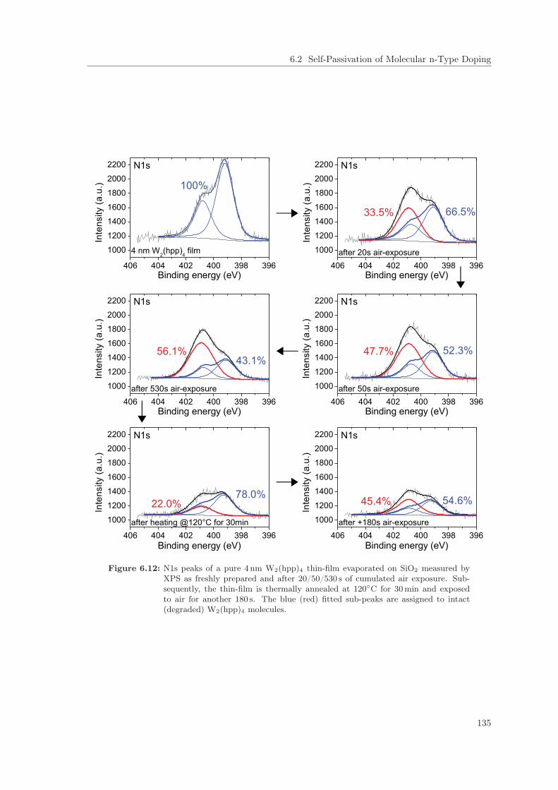
6.2 Self-Passivation of Molecular n-Type Doping
Figure 6.12: N1s peaks of a pure 4 nm W2(hpp)4 thin-film evaporated on SiO2 measured byXPS as freshly prepared and after 20/50/530 s of cumulated air exposure. Sub-sequently, the thin-film is thermally annealed at 120◦C for 30 min and exposedto air for another 180 s. The blue (red) fitted sub-peaks are assigned to intact(degraded) W2(hpp)4 molecules.
135

6 Investigations on Molecular n-Doping
LDI-TOF measurements on pure W2(hpp)4
The degradation of W2(hpp)4 thin-films in air is investigated by LDI-TOF-MS.5 The analysis of anun-degraded reference W2(hpp)4 thin-film is not possible since every LDI-TOF sample is exposedto air for approximately 50 s while transferring it into the spectrometer. However, the degradationunder air exposure times above 1 minute can be reliably investigated.A respective LDI-TOF mass spectrum of a 2 nm W2(hpp)4 thin layer on gold that is exposed for3 minutes to air prior the measurement is shown in Fig. 6.13 (a). Several degradation productsare identified. Besides complete W2(hpp)4 molecules (921.8 u), a strong desorption peak of thehexahydropyrimidopyrimidine ligant [hpp] (139.7 u) and a small peak of di-tungsten W2 (377.4 u),as well as of [hpp+O] (156.0 u), [W(hpp)2+O] (478.1 u), and [W(hpp)3] (598.9 u) are visible in thespectrum. Thus, it can be concluded that the dopant molecules partly broke by cleavage of the W-Nand W-W bonds as the initial quick degradation process. Subsequently, the degradation fragmentsfurther oxidize which is in agreement with the findings from XPS. Although [hpp+O] fragments arefound, surprisingly no tungsten oxide WOx is present in the degraded film. Additionally, the [hpp]”paddle” (139.7 u) seems to be stable and does not decompose to even smaller molecular fragments(or these are volatile in vacuum).To verify the (exposure time dependent) XPS findings of Fig. 6.11 and Fig. 6.12, samples with 2 nmlayers of W2(hpp)4 evaporated either on a 20 nm gold or on a 50 nm C60 sub-layer are investigatedstepwise under accumulated 50, 170, 310, and 550 s of air exposure. Regardless of the substratethe same degradation products with similar relative peak intensities are found for all LDI-TOF-MSmeasurements. The normalized peak intensities of complete W2(hpp)4 signals as well as the signal ofthe [W(hpp)2+O] degradation product are plotted in Fig. 6.13 (b) versus the cumulated air exposuretime. Whereas the former exponentially decreases, the degradation product intensity increases to afinal value I(t→∞). Fitting the signal decay of intact W2(hpp)4 by
I(t) = Ad · exp(− t
τd
)(6.2)
yields Ad = 1.07 and a decay constant τd = 10.6min for W2(hpp)4 on Au and 10.1 min for W2(hpp)4on C60. The growth of the [W(hpp)2+O] fragment peak intensity is in congruence with this result.Fitting the single exponential growth function
I(t) = I(t→∞)−Ag · exp(− t
τg
)(6.3)
to the normalized intensity, i.e. setting I(t→∞) = 1, yields Ag = 0.51 and τg = 11.2min which isin good agreement with the decay time obtained from the W2(hpp)4 peak. However, since severalother degradation fragments have also been observed, both constants must not necessarily be equal,because the different reaction channels to the finally formed fragments with oxygen are unknown.Nevertheless, the fragment [W(hpp)2 +O] just equals an oxidized half original W2(hpp)4 moleculeand a further decomposition of this species, e.g. to [W(hpp) + O], is not present in the LDI-TOF
5Laser Desorption Ionization - Time of Flight - Mass Spectroscopy: Details of the experimental setup are describedin Sec. 4.4.3. The measurements are performed by Florian Wölzl at the IAPP.
136

6.2 Self-Passivation of Molecular n-Type Doping
τ
τ
Figure 6.13: (a) LDI-TOF-MS spectrum of a degraded 2 nm W2(hpp)4 thin-film on gold. Thesample was exposed for 3 minutes to air prior the measurement. (b) Decay ofthe W2(hpp)4 signal versus the cumulative air exposure time of 2 nm W2(hpp)4evaporated either on gold or a C60 interlayer. Additionally, the evolution of thecorresponding W(hpp)2 + O degradation fragment is plotted. The Intensities areeach normalized to the corresponding initial W2(hpp)4 and final W(hpp)2 + Ovalues, and the signals are fitted by exponential functions (red lines) with thegrowth (decay) constants τg (τd).
spectrum of Fig. 6.13 (a). Thus, it is reasonable to assume that the decay channel
W2(hpp)4 +O2 → 2 · [W(hpp)2 +O] (6.4)
most likely exhibits equal decay/growth constants τd/τg, which is confirmed by our measurements.An even more comprehensive and quantitative analysis of the W2(hpp)4 degradation is impossiblesince the LDI cross sections of the various fragments are unknown which therefore prevents anabsolute comparison of the different peak intensities.It can be seen in Fig. 6.13 (b) that approximately 51% of the degradation product [W(hpp)2+O]is already formed at t ≈ 0 (fitted Ag = 0.51). A very quick initial degradation of W2(hpp)4molecules within the first seconds of air exposure can therefore be concluded although no LDI-TOFspectra of films exposed to air for below 1 minute are accessible by the experimental setup. Theremaining complete W2(hpp)4 molecules stay intact and further degrade exponentially on a scaleof several minutes. These observations strongly support the qualitative results obtained from XPS(cf. Fig. 6.11).
6.2.2 Passivation of W2(hpp)4 in C60: Improvement by intrinsic Cover Layer
Interestingly, the observed protection effect of W2(hpp)4 within n-C60 films against degradationcan be improved by coverage with an intrinsic C60 cover layer and subsequent thermal annealingprior to the exposure to air. This effect was found during investigations on a respective UPS/XPSsample, which was originally built for studying the diffusion of dopants under heat treatment. The
137

6 Investigations on Molecular n-Doping
used sample structure reads: Au/C60:W2(hpp)4 (16 wt%, 8 nm)/C60 (6 nm). It is incrementallyevaporated and measured by UPS and XPS. After deposition of the 6 nm C60, layer the sample isannealed at 135◦C for 1 h under UHV conditions and subsequently exposed to air for cumulated20/60/360/600 s.The obtained W4f and N1s core level peaks originating from the W2(hpp)4 molecules are plottedin Fig. 6.14 and Fig. 6.15, respectively. Since the XPS probing depth decays exponentially with thelayer thickness, evaporation of the pure C60 top layer leads to a decrease of both peaks in comparisonto the signal of the n-C60 film underneath. The N1s peak even vanishes. However, after heating bothcore levels reappear with peaks at the same energetic positions, e.g. W4f5=34.95 eV (L:G=55 %),W4f7=32.76 eV (L:G=84 %). Furthermore, the absolute peak intensities are approximately recovered
Figure 6.14: W4f peak of an incrementally built Au/C60:W2(hpp)4 (16 wt%, 8 nm)/C60 (6 nm)structure. Prior exposing the sample to air, it has been heated for 1 h at 135◦C.The cumulated air exposure times are 20/60/600 s.
138
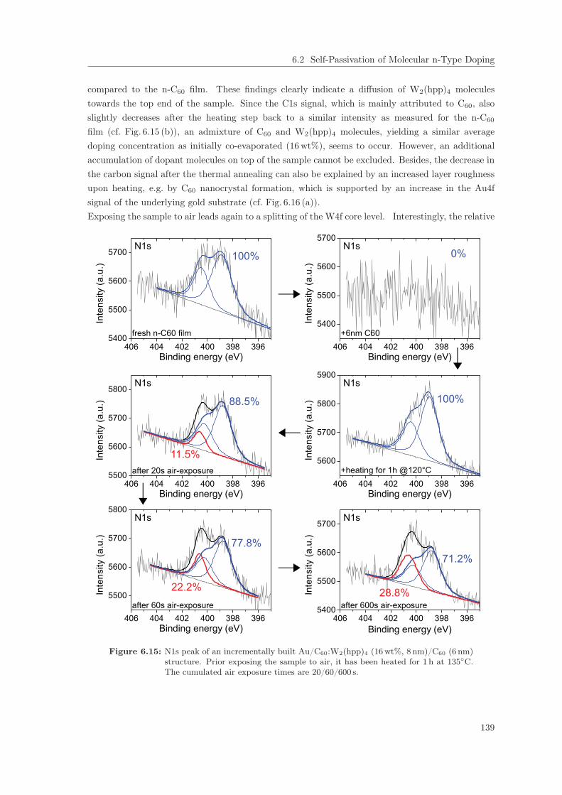
6.2 Self-Passivation of Molecular n-Type Doping
compared to the n-C60 film. These findings clearly indicate a diffusion of W2(hpp)4 moleculestowards the top end of the sample. Since the C1s signal, which is mainly attributed to C60, alsoslightly decreases after the heating step back to a similar intensity as measured for the n-C60
film (cf. Fig. 6.15 (b)), an admixture of C60 and W2(hpp)4 molecules, yielding a similar averagedoping concentration as initially co-evaporated (16 wt%), seems to occur. However, an additionalaccumulation of dopant molecules on top of the sample cannot be excluded. Besides, the decrease inthe carbon signal after the thermal annealing can also be explained by an increased layer roughnessupon heating, e.g. by C60 nanocrystal formation, which is supported by an increase in the Au4fsignal of the underlying gold substrate (cf. Fig. 6.16 (a)).Exposing the sample to air leads again to a splitting of the W4f core level. Interestingly, the relative
Figure 6.15: N1s peak of an incrementally built Au/C60:W2(hpp)4 (16 wt%, 8 nm)/C60 (6 nm)structure. Prior exposing the sample to air, it has been heated for 1 h at 135◦C.The cumulated air exposure times are 20/60/600 s.
139

6 Investigations on Molecular n-Doping
Figure 6.16: C1s (a) and W4f (b) core levels of an incrementally built Au/C60:W2(hpp)4(16 wt%, 8 nm)/C60 (6 nm) structure. Prior exposing the sample to air, it hasbeen heated for 1 h at 135◦C. The cumulated air exposure times are 20/60/600 s.
amount of signal attributed to still intact dopants is much larger than observed for the sampleswithout the cover layer and pre-heating step (cf. Fig. 6.10). Fitting the W4f signal after 20 s ofair exposure yields 80.4 % intact W2(hpp)4 molecules. Extending the exposure time to 10 minutesdecreases this ratio only to 56.6 %. In case of the N1s peak, the corresponding fitted relativeamounts are 88.5 % and 71.2 %, respectively. In comparison, for the simple Au/n-C60 structure only20.0 % of the W4f signal can be attributed to intact dopants after an air exposure of just 60 s. Asexplanation, it is not reasonable to assume that only the thin C60 cover layer prevents a diffusionof oxygen towards the n-C60 film underneath during the air exposure as a kind of barrier. It seemsmore plausible that the thermal annealing accompanied by an enhanced admixture of dopant andhost molecules provide the improved protection mechanism.The findings from XPS are confirmed by UPS which is illustrated in Fig. 6.17. Due to n-doping,the spectrum of the first n-C60 film is shifted towards the LUMO (EF = 2.88 eV) and possessestypical gap state features which are vanished for the 6 nm intrinsic C60 cover layer on top, yieldingin contrast a well defined Gaussian DOS shape (gray line). Interestingly, the spectrum is notsignificantly shifted back into the gap (EF = 2.77 eV), which indicates a diffusion of free electronsgenerated in the n-doped layer into the undoped top layer. For comparison, an intrinsic C60 layerevaporated directly on gold yields EF = 2.25 eV. The shape of the spectrum completely changesafter the thermal annealing step, possessing more or less the same shape as measured for the first n-C60 film. The Fermi level is even shifted slightly towards the LUMO (EF = 2.83 eV). Furthermore,strongly pronounced gap states are present with a much broader spectral shape as that of the firstn-C60 film (cf. inset Fig. 6.17 (a), blue line).Exposing the sample subsequently to air for 20/60/360/600 s leads to a decrease of only that gapstates which are close to the Fermi level. Even after 10 minutes a significant amount of gap statesis still present, indicating an intact n-doping effect. Also the Fermi level shifts comparably slowlyaway from the LUMO upon air exposure. The positions are 2.76/2.70/2.66 eV above the HOMO-peak after 20/60/360 s (cf. Fig. 6.17 (b)). After 600 s of cumulated air exposure the Fermi level hasthe same position as a doped film with one hundredths of the molar doping ratio (EF = 2.62 eV).This finding demonstrates on the one hand that the molecular n-doping is partially still intact.However, on the other hand it seems that the estimation of the relative amount of intact W2(hpp)4
140

6.2 Self-Passivation of Molecular n-Type Doping
Figure 6.17: (a) UPS spectra of an an Au/C60:W2(hpp)4 (16 wt%, 8 nm)/C60 (6 nm) structurebefore and after thermal annealing at 135◦C for 1 h in vacuum. Subsequently, thesample has been exposed to air for cumulated 20/60/360/600 s.(b) Determined Fermi level positions for the consecutive air exposure steps (blacksymbols) compared to other doping concentration samples.
molecules based on the W4f peak fit shown above yields actually an over estimation or the actualdoping efficiency is very low. Reasons for these deviations will be discussed in Sec. 6.3, taking theexperimental findings of the other host materials into account.
6.2.3 Host Material Variation
To get a deeper insight into the underlying physics of the passivation mechanism of W2(hpp)4 inthin-films, n-doped films using various host materials with different LUMO energies are investigated:Pentacene (EA = 2.6 eV), ZnPc (EA = 3.4 eV), Bis-HFl-NTCDI (CV LUMO = −3.8 eV6), andthe proprietary host material NET1087 (EA ≈ 4.0 eV8). Conductivity and systematic UPS/XPSmeasurements are performed for each material combination under air exposure.
Pentacene:W2(hpp)4
The conductivity of a 60 nm pentacene film doped by 16 wt% W2(hpp)4 is plotted in Fig. 6.18 (a)versus the exposure time to air. Prior the air exposure, an initial value of σ = 6.3 × 10⁻³ S/cm ismeasured in a N2 glovebox which is directly connected to the high vacuum evaporation chamber.However, immediately after exposing the sample to air, the conductivity parabolically decreases,reaching the resolution limit of the setup of approximately 2 × 10⁻⁶ S/cm within 5 minutes. After10 minutes, the sample is transferred back into the glovebox and heated on a hotplate at 120◦ for35 minutes. However, a recovery of the conductivity, as observed for the C60:W2(hpp)4 thin-film (cf.Fig. 6.6), is not found here. The measured current remains in the resolution limit of the setup (data6Source: OSOL database, measured by Markus Hummert.7Novaled Electron Transporter 1088Jan Blochwitz-Nimoth, CSO Novaled GmbH: Personal communication.
141

6 Investigations on Molecular n-Doping
σ
Figure 6.18: (a) Conductivity of a P5:W2(hpp)4 (60 nm, 16 wt%) thin-film during air exposure.The initial value of σ = 0.0063 S/cm was measured in a N2 glovebox rather thanunder vacuum conditions. (b) Relative amounts of W4f XPS signals assigned tointact W2(hpp)4 molecules in various n-doped thin-films or purely evaporated onSiO2 versus the air exposure time.
not shown), which strongly indicates that most of the W2(hpp)4 molecules decomposed in air and non-doping effect to the P5 host is active. However, the resolution limit of the measurement setup isjust three orders of magnitude below the initially measured conductivity. Therefore, it could also bepossible that either a small amount of maximal 0.1 % of the W2(hpp)4 molecules is still passivatedor that electron trap states of very high density are generated by the air exposure from which theconductivity suffers (even after thermal annealing).For clarification, an n-doped pentacene thin-film is measured by UPS since the Fermi level posi-tion correlates directly with the number of free electrons n. In correspondence to the n-dopingstudy presented in Sec. 6.1.2, the used sample structure is: Ag/MeO-TPD(4 nm)/P5:W2(hpp)4(35 nm, 16 wt% (MR = 0.058)). The sample is exposed to air stepwise for accumulated 15/75/375 s.The corresponding UPS spectra are shown in Fig. 6.19 (a) and the determined Fermi level positionsare plotted in Fig. 6.19 (b) (blue symbols) in comparison to that of freshly prepared samples withother doping concentrations. Already after only 15 s of air exposure, the thin-film spectrum is shiftedby 0.23 eV towards lower binding energies and the Fermi level lies 2.44 eV above the HOMO-peak.The gap states, attributed to n-doping, completely vanish (cf. inset of Fig. 6.19 (a)). After an ex-posure time of 375 s, EF = 2.36 eV is obtained, which on the one hand is well above the value fora respective undoped sample (EF ≈ 1.8 eV), but significantly below the value of a freshly preparedsample with MR = 6.7 × 10⁻⁴ (EF = 2.48 eV, cf. Fig. 6.19 (b)). This finding strongly supportsthe above hypothesis that within the pentacene matrix, most of the W2(hpp)4 molecules are notpassivated against degradation.The W4f as well as the C1s core levels of the P5:W2(hpp)4 thin-film are additionally scanned byXPS after each air exposure step (cf. Fig. 6.20). The C1s peak is shifted by approximately 0.30 eVto lower binding energies upon air exposure, which corresponds to the respective increase in the film
142

6.2 Self-Passivation of Molecular n-Type Doping
Figure 6.19: (a) Evolution of UPS spectra of an Ag/MeO-TPD(4 nm)/P5:W2(hpp)4(35 nm, 16 wt% (MR = 0.058)) sample under 0/15/75/375 s of cumulated air ex-posure. For comparison a respective undoped pentacene thin-film spectrum isshown.(b) Determined Fermi level positions for the consecutive air exposure steps (bluesymbols) compared to other doping concentration samples.
work function, i.e. no drastic changes in the bonding states of the respective carbon atoms appear.Also the peak shape remains practically unchanged. Since the C1s signal originates mainly from thehost material, it can be concluded that the pentacene molecules are not affected by the air exposureand stay stable. Hence, the observed drop in conductivity must be attributed to a degradation ofthe n-dopants. Indeed, the W4f signal of the W2(hpp)4 molecules splits again into two doubletsalready after 15 s of air exposure. Here, the relative amount of the intact species (blue doublet) isjust 23.1%, and decreases slowly further to finally 18.3 % after an exposure time of cumulated 375 s.A similar behavior was already found for the pure W2(hpp)4 film on SiO2. For comparison, the re-spective relative intensities of the W4f doublets attributed to intact W2(hpp)4 molecules are plottedversus the air exposure time in Fig. 6.18 (b). A strong decay is found within the first seconds forboth types of samples. Within the subsequent minutes, the signal decays only very slowly. However,it is surprising that although approximately 20 % of the dopant molecules seem to be still intact,it has been concluded from the Fermi level position that only maximal 0.1 % of the initial dopantsprovide an n-doping effect after the exposure to air. This discrepancy will be discussed below inmore detail by considering the experimental results of the other material combinations.
143

6 Investigations on Molecular n-Doping
Figure 6.20: (a) Evolution of the W4f peak signal of an Ag/MeO-TPD(4 nm)/P5:W2(hpp)4(35 nm, 16 wt%) sample under 0/15/75/375 s of cumulated air exposure. The blue(red) fitted double peaks are assigned to intact (degraded) W2(hpp)4 molecules.The relative intensity amounts are indicated by colored number. (b) Correspond-ing C1s peaks.
144

6.2 Self-Passivation of Molecular n-Type Doping
ZnPc:W2(hpp)4
Next, the air stability of the system ZnPc:W2(hpp)4 is investigated. For that, the conductivity ofan n-doped thin-film (36 nm, 18 wt% (MR = 0.14)) is measured while exposing the sample to air (cf.Fig. 6.21 (a)).9 The freshly prepared film possesses a conductivity of 0.011 S/cm in vacuum. Im-mediately after exposing the sample to air, the conductivity drops by several orders of magnitude,reaching the experimental resolution limit of approximately 10−9 S/cm within a few seconds. Simi-larly to experiments with n-doped C60, the measurement chamber is re-evacuated after 16minutes,which however, does not show any (restoration) effect on the conductivity. Subsequently, the sam-ple is slowly heated to 120◦C and kept at this temperature for 1 h. The corresponding measuredconductivity is show in Fig. 6.21 (b). Only a marginal increase to σ ≈ 10−7 S/cm is observed, whichis still five orders of magnitude below the initial value of the fresh sample. This finding clearlydemonstrates that the n-doping effect of W2(hpp)4 to ZnPc is not protected against degradation inair.
σ
Figure 6.21: Conductivity of a ZnPc:W2(hpp)4 (36 nm, 18 wt%) thin-film during air exposure(a) and heating after re-evacuation (b). The initial value of σ = 0.011 S/cm ismeasured under vacuum conditions. The measurements are performed by SteffenPfützner at Novaled AG (Dresden, Germany).
This conclusion is confirmed by UPS measurements. Here, an n-doped ZnPc film (10 nm, 18wt%)is evaporated on silver and stepwise exposed to air for cumulated 15/555/1095 s. The obtainedUPS spectra are shown in Fig. 6.22 (a) in comparison to an undoped ZnPc sample. After 15 s ofair exposure, the spectrum of the n-doped film is shifted by 0.30 eV to lower binding energies, i.e.the Fermi level shits from 2.11 eV above the HOMO-peak position to EF = 1.81 eV. Again, then-doping related gap states (cf. inset of Fig. 6.22 (a)) completely disappear. Exposing the samplefor additional 9 minutes to air (cumulated 555 s) decreases the Fermi level position even more toEF = 1.65 eV which is already close to that of the undoped sample. An air exposure of further9 minutes (cumulated 1095 s) shifts the spectrum to EF = 1.58 eV which is equal to the undoped
9The measurements are performed by Steffen Pfützner at Novaled GmbH (Dresden, Germany).
145

6 Investigations on Molecular n-Doping
Figure 6.22: (a) Evolution of UPS spectra of an Ag/ZnPc:W2(hpp)4 (10 nm, 18 wt%) sampleunder 0/15/555/1095 s of cumulated air exposure. For comparison a respectiveundoped ZnPc thin-film spectrum is shown. (b) Determined Fermi level positionsfor the consecutive air exposure steps (red symbols) compared to other dopingconcentration samples.
position. The determined Fermi level positions are compared to that of samples with varied molardoping ratios in Fig. 6.22 (b). Already after the first 15 s of air exposure, the Fermi level lies belowvalues measured for doping concentrations of one hundredths, i.e. only maximal 1% of the initialW2(hpp)4 molecules still provide free electrons by n-doping. Since the shape of the ZnPc HOMO-peak does not change upon air exposure, it can be concluded that the host molecules stay stable inair.This presumption is supported by C1s and Zn2p3 core level scans shown in Fig. 6.23. Only the peakpositions shift by 0.4 eV towards lower binding energies which coincides with the respective changein the film work function. The peak shapes are nearly unaffected by the air exposure, which stronglyindicates stability of the ZnPc host in air. In contrast, drastic changes are found again for the W4f
Figure 6.23: Evolution of the Zn2p3 and C1s peaks of an Ag/ZnPc:W2(hpp)4 (10 nm, 18 wt%)sample under 0/15/195/555/1095 s of cumulated air exposure.
146

6.2 Self-Passivation of Molecular n-Type Doping
core level signal originating from the dopant molecules (cf. Fig. 6.24). The well defined double peakof the fresh film (W4f7=32.66 eV, W4f5=34.77 eV, ratio 4:3) splits into two doublets which are againassigned to intact (33.1%, blue doublet) and degraded (66.9%, red doublet) W2(hpp)4 molecules.With increasing air exposure time, the relative amount of intact dopants decreases monotonouslyto 18.9% after cumulated 1095 s. For comparison to the other host materials, this value is plottedinto Fig. 6.18 (b), fitting well to the data obtained for P5:W2(hpp)4. The slight increase at the lastdata point (air exposure time of ≈ 18min) can be attributed to fitting uncertainties. However, theZnPc:W2(hpp)4 sample clearly confirms the already found behavior of an initial rapid degradationof most of the dopants within a few seconds, followed by a much slower decay on a time scale of afew minutes.
Figure 6.24: (a) Evolution of the W4f peak signal of an Ag/ZnPc:W2(hpp)4 (10 nm, 18 wt%)sample under 0/15/195/285/1095 s of cumulated air exposure. The blue (red)fitted double peaks are assigned to intact (degraded) W2(hpp)4 molecules. Therelative intensity amounts are indicated by colored number.
147

6 Investigations on Molecular n-Doping
Bis-HFl-NTCDI:W2(hpp)4
The next investigated material combination is Bis-HFl-NTCDI:W2(hpp)4, for which a similar pas-sivation effect as observed in the n-C60 films is found. The conductivity during air exposure for30 minutes of a 35 nm Bis-HFl-NTCDI thin-film doped by 7 wt% of W2(hpp)4 (MR = 0.05) is shownin Fig. 6.25 (a). Starting at an initial value of σ = 9.4 × 10⁻⁴ S/cm measured in situ under highvacuum conditions, the conductivity immediately drops after ventilating the chamber with ambi-ent air. However, the observed decrease is much weaker than for n-doped ZnPc, P5, or C60 films.The conductivity drops only by a factor of two within 5minutes of air exposure and subsequentlydecreases only very slowly to 3.1 × 10⁻⁵ S/cm during the following 25 minutes, i.e. to 33% of theinitial value. This finding is remarkable since it means that the n-doping effect is practically activeeven in air and also not hindered by trap formation. Re-evacuation of the measurement chamberslightly increases the conductivity to 4.4× 10⁻⁵ S/cm within 1 h. Furthermore, a thermal annealingat 120◦C for an additional hour and re-cooling to room temperature recovers the conductivity to2.0 × 10−4, which is even twice as high as the conductivity of the freshly prepared thin-film (cf.Fig. 6.25). This result means that either the n-doping is thermally activated even more or/and thatthe layer morphology is advantageously modified, from which the electron mobility benefits. SinceIP(W2(hpp)4) = 2.4 eV < EA(Bis-HFl-NTCDI) ≈ 3.8 eV, efficient electron transfer to NTCDI hostmolecules within n-doped thin-films can be expected without any further possible improvementby thermal activation. Hence, the observed increase in conductivity above the initial value orig-inates most likely from a morphology effect. This presumption is supported by measurements ofChristiane Falkenberg on similar Bis-HFl-NTCDI:Cr2(hpp)4 (7.5 wt%) films evaporated on a heatedsubstrate. [282] A conductivity of 2.5×10⁻³ S/cm was found which is roughly one order of magnitudehigher than that of a respective film evaporated on a room temperature substrate (4.1×10⁻⁴ S/cm).An additional dopant activation by subsequent heating could not be observed. [282]
σ
σ
σ
σ
Figure 6.25: (a) Conductivity of a Bis-HFl-NTCDI:W2(hpp)4 (35 nm, 7 wt%) thin-film duringair exposure (a) and thermal annealing after re-evacuation (b). The initial valueof σ = 9.4× 10⁻⁵ S/cm is measured under vacuum conditions.
148
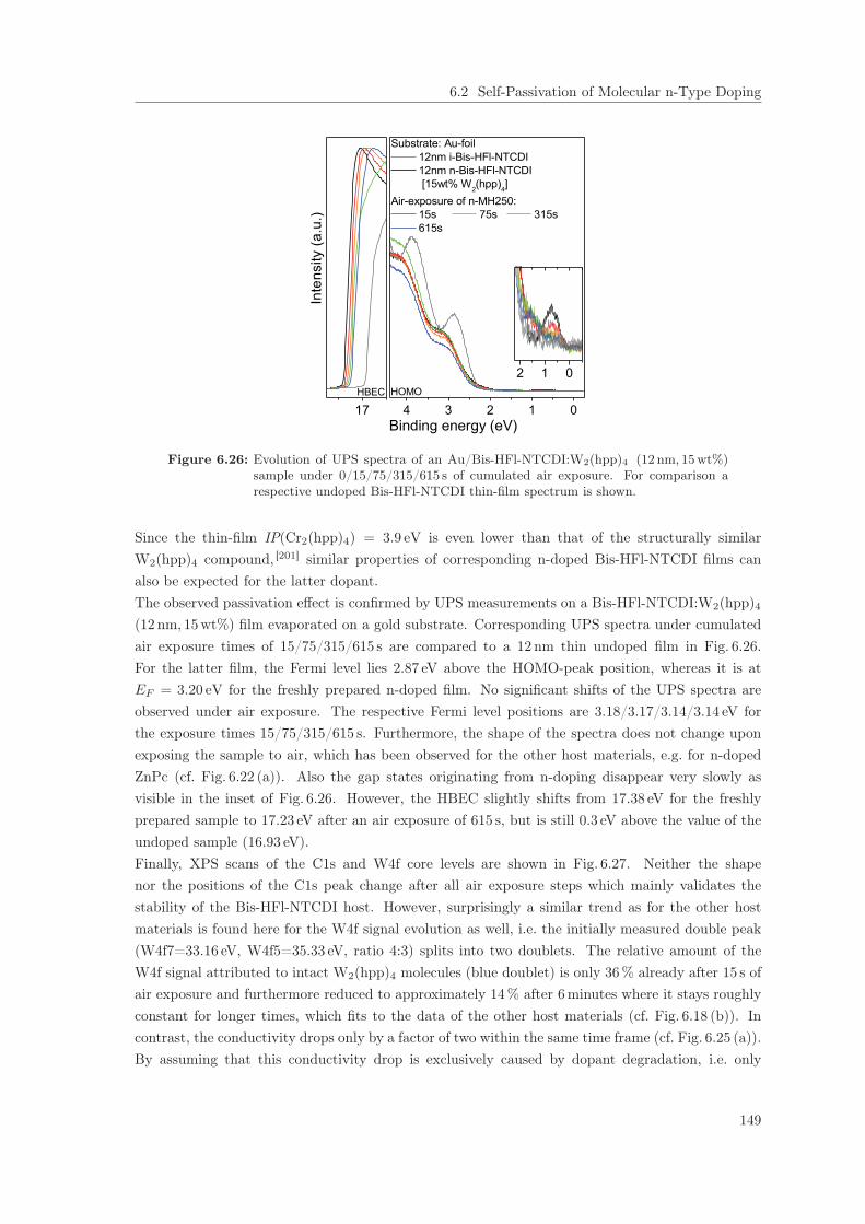
6.2 Self-Passivation of Molecular n-Type Doping
Figure 6.26: Evolution of UPS spectra of an Au/Bis-HFl-NTCDI:W2(hpp)4 (12 nm, 15 wt%)sample under 0/15/75/315/615 s of cumulated air exposure. For comparison arespective undoped Bis-HFl-NTCDI thin-film spectrum is shown.
Since the thin-film IP(Cr2(hpp)4) = 3.9 eV is even lower than that of the structurally similarW2(hpp)4 compound, [201] similar properties of corresponding n-doped Bis-HFl-NTCDI films canalso be expected for the latter dopant.The observed passivation effect is confirmed by UPS measurements on a Bis-HFl-NTCDI:W2(hpp)4(12 nm, 15 wt%) film evaporated on a gold substrate. Corresponding UPS spectra under cumulatedair exposure times of 15/75/315/615 s are compared to a 12 nm thin undoped film in Fig. 6.26.For the latter film, the Fermi level lies 2.87 eV above the HOMO-peak position, whereas it is atEF = 3.20 eV for the freshly prepared n-doped film. No significant shifts of the UPS spectra areobserved under air exposure. The respective Fermi level positions are 3.18/3.17/3.14/3.14 eV forthe exposure times 15/75/315/615 s. Furthermore, the shape of the spectra does not change uponexposing the sample to air, which has been observed for the other host materials, e.g. for n-dopedZnPc (cf. Fig. 6.22 (a)). Also the gap states originating from n-doping disappear very slowly asvisible in the inset of Fig. 6.26. However, the HBEC slightly shifts from 17.38 eV for the freshlyprepared sample to 17.23 eV after an air exposure of 615 s, but is still 0.3 eV above the value of theundoped sample (16.93 eV).Finally, XPS scans of the C1s and W4f core levels are shown in Fig. 6.27. Neither the shapenor the positions of the C1s peak change after all air exposure steps which mainly validates thestability of the Bis-HFl-NTCDI host. However, surprisingly a similar trend as for the other hostmaterials is found here for the W4f signal evolution as well, i.e. the initially measured double peak(W4f7=33.16 eV, W4f5=35.33 eV, ratio 4:3) splits into two doublets. The relative amount of theW4f signal attributed to intact W2(hpp)4 molecules (blue doublet) is only 36 % already after 15 s ofair exposure and furthermore reduced to approximately 14 % after 6minutes where it stays roughlyconstant for longer times, which fits to the data of the other host materials (cf. Fig. 6.18 (b)). Incontrast, the conductivity drops only by a factor of two within the same time frame (cf. Fig. 6.25 (a)).By assuming that this conductivity drop is exclusively caused by dopant degradation, i.e. only
149

6 Investigations on Molecular n-Doping
by reduction in the charge carrier density n, as well as that the still intact W2(hpp)4 molecules(relatively 14 %) purely provide the whole n-doping effect in air, these findings mean that the initialdoping efficiency ηdop = n/ND must have been at best 2×14% = 28%. This conclusion contradictsto the results of the n-doping studies on C60, ZnPc and P5 discussed in Sec. 6.1.2 where dopantsaturation was concluded for all material systems. Furthermore, it seems to be inconsistent thatthe decay of the "intact" W4f core levels is similar for all investigated hosts as well as for pureW2(hpp)4 in air (cf. Fig. 6.18 (b)) although the conductivity and UPS measurements reveal quitedifferent protection strengths against degradation.
Figure 6.27: (a) Evolution of the W4f peak signal of an Au/Bis-HFl-NTCDI:W2(hpp)4(12 nm, 15 wt%) sample under 0/15/75/315/615 s of cumulated air exposure.The blue (red) fitted double peaks are assigned to intact (degraded) W2(hpp)4molecules. The relative intensity amounts are indicated by colored number. (b)Corresponding C1s peaks.
150
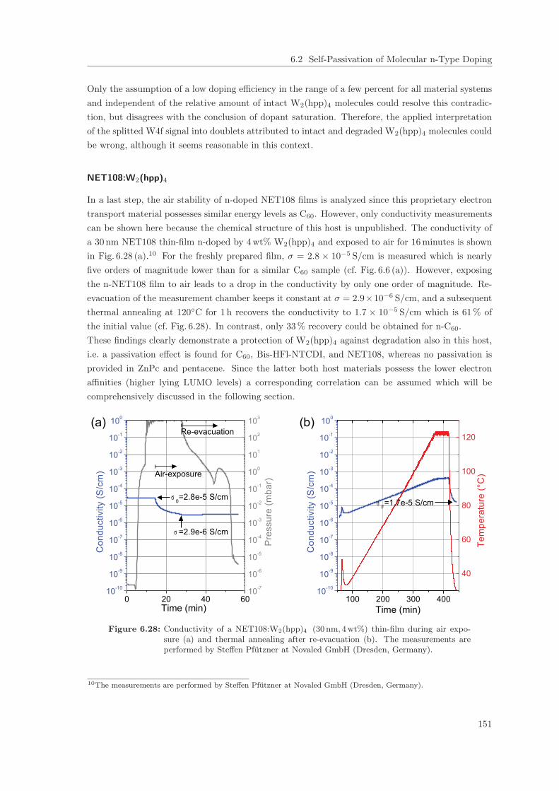
6.2 Self-Passivation of Molecular n-Type Doping
Only the assumption of a low doping efficiency in the range of a few percent for all material systemsand independent of the relative amount of intact W2(hpp)4 molecules could resolve this contradic-tion, but disagrees with the conclusion of dopant saturation. Therefore, the applied interpretationof the splitted W4f signal into doublets attributed to intact and degraded W2(hpp)4 molecules couldbe wrong, although it seems reasonable in this context.
NET108:W2(hpp)4
In a last step, the air stability of n-doped NET108 films is analyzed since this proprietary electrontransport material possesses similar energy levels as C60. However, only conductivity measurementscan be shown here because the chemical structure of this host is unpublished. The conductivity ofa 30 nm NET108 thin-film n-doped by 4wt% W2(hpp)4 and exposed to air for 16 minutes is shownin Fig. 6.28 (a).10 For the freshly prepared film, σ = 2.8 × 10⁻⁵ S/cm is measured which is nearlyfive orders of magnitude lower than for a similar C60 sample (cf. Fig. 6.6 (a)). However, exposingthe n-NET108 film to air leads to a drop in the conductivity by only one order of magnitude. Re-evacuation of the measurement chamber keeps it constant at σ = 2.9×10⁻⁶ S/cm, and a subsequentthermal annealing at 120◦C for 1 h recovers the conductivity to 1.7 × 10⁻⁵ S/cm which is 61 % ofthe initial value (cf. Fig. 6.28). In contrast, only 33% recovery could be obtained for n-C60.These findings clearly demonstrate a protection of W2(hpp)4 against degradation also in this host,i.e. a passivation effect is found for C60, Bis-HFl-NTCDI, and NET108, whereas no passivation isprovided in ZnPc and pentacene. Since the latter both host materials possess the lower electronaffinities (higher lying LUMO levels) a corresponding correlation can be assumed which will becomprehensively discussed in the following section.
σ
σ
σ
Figure 6.28: Conductivity of a NET108:W2(hpp)4 (30 nm, 4 wt%) thin-film during air expo-sure (a) and thermal annealing after re-evacuation (b). The measurements areperformed by Steffen Pfützner at Novaled GmbH (Dresden, Germany).
10The measurements are performed by Steffen Pfützner at Novaled GmbH (Dresden, Germany).
151
6 Investigations on Molecular n-Doping
6.3 Conclusions on the Molecular Doping Mechanism
In summary, the experiments on molecular n-doping with the di-metal complex W2(hpp)4 yieldthe following results. At high doping concentrations, the Fermi level shifts close or even above theLUMO-onset for all three investigated host materials. In contrast, it was pinned a few 100 meVabove the HOMO-onset at an assumed effective acceptor level EA in case of p-doping, i.e. dopantreserve was concluded there. Here, the Fermi level shift upon n-doping is calculated by assum-ing dopant saturation for all concentrations, i.e. assuming a constant doping efficiency of 100 %(n = N+
D = ND). Since the LUMO DOS parameter cannot be fitted sufficiently accurate enough,just Gaussian distributions with widths in the range of σ = 0.07 . . . 0.15 eV are used in the calcu-lations, which yields reasonable fits to the experimental UPS data. Assuming an effective donorlevel ED is not necessary, i.e. it must actually lie very close to the LUMO. Furthermore, gap statesappear in the UPS spectra at doping concentrations of MR ≈ 0.01 and higher. These states increasein intensity with rising molar ratio, which is illustrated in Fig. 6.29. There, spectra of n-doped pen-tacene, ZnPc, and C60 films, normalized and rescaled in energy to the respective HOMO-peaks (setto E = 0), are plotted for various doping concentrations. At molar ratios above 0.1, the GaussianHOMO-peaks of the host materials are strongly superimposed by the gap state features. Further-more, a continuous increase in signal at higher binding energies is found, which completely changesthe spectral shape at the highest doping concentrations (cf. red lines in Fig. 6.29).Since the dopant material W2(hpp)4 is unstable in air as powder due its low ionization potential of2.4 eV, [198] respective degradation experiments were performed and a partial protection of W2(hpp)4molecules within n-doped thin-films against degradation was found. Surprisingly, this passivationeffect seems to depend on the energy levels of the used host material, since in hosts with compa-rably low electron affinities it does not work, e.g. in ZnPc (3.4 eV) and pentacene (2.6 eV), whereasthe n-doping effect is (partially) passivated in C60 (4.2 eV), Bis-HFl-NTCDI (LUMO=-3.8 eV), andNET108 (≈ 4.0 eV). This hypothesis has been confirmed by conductivity and UPS measurements.However, the decay in the W4f core level peak attributed to intact W2(hpp)4 molecules after airexposure is quite similar for all investigated host systems as well as for a pure dopant film (cf.Fig. 6.18 (b)). The experiments furthermore revealed that the degradation of W2(hpp)4 occurs ontwo different time scales. More than half of the dopant molecules are decomposing immediatelyafter an exposure to air, whereas the remaining intact W2(hpp)4 molecules further degrade veryslowly. For pure W2(hpp)4 films, an exponential decay constant of approximately 10minutes couldbe identified by LDI-TOF-MS. However, the remaining amount of un-degraded dopant moleculesis sufficiently large to provide a significant n-doping effect in C60, Bis-HFl-NTCDI, and NET108,even after 30 minutes of air exposure. The gap states, which arise upon n-doping, disappear withina few seconds after exposing the samples to air for all material combinations except as for n-Bis-HFl-NTCDI films. Here, the gap state features decreases in intensity on an exposure time scale ofa few minutes. Finally, it was found that the passivation effect seems to be stronger in pre-heatedsamples, e.g. within an Au/n-C60/i-C60 structure (cf. Fig. 6.18 (b), upside down triangles). In thefollowing, physical reasons for the unexpected protection of W2(hpp)4 molecules against oxidationwithin the investigated thin-films are discussed.
152

6.3 Conclusions on the Molecular Doping Mechanism
Figure 6.29: UPS spectra of pentacene, ZnPc and C60 thin-films n-doped by W2(hpp)4 varyingthe doping concentration by four orders of magnitude. The spectra are normalizedto the HOMO-peak positions and superimposed such that the peaks of all samplesare rescaled to E = 0.
Due to electron transfer to host molecules, W2(hpp)4 molecules become ionized which changes theirenergy levels. In case of the W2(hpp)
+4 cation, this corresponds to an effectively enlarged ioniza-
tion potential compared to the neutral W2(hpp)4 molecule upon re-arrangement of the remainingoccupied molecular orbitals. If the increase in the IP is sufficiently high, this effect might explainthe protection of W2(hpp)4 against degradation in air. However, to effectively protect the n-dopantagainst degradation, an increase of the IP by more than 1.5 eV is necessary to overcome the oxida-tion potential of oxygen. [13] Whether the re-arrangement of the molecular orbitals of W2(hpp)4 afterionization is sufficient to cause such a strong change in the IP could be quantified by density func-tional calculations which is, however, out of scope of the discussion here. However, for comparison,energy level shifts of up to 2 eV upon ionization were published for TTF-TCNQ compounds. [316]
However, this reasoning cannot explain the dependence of the protection effect on the host LUMOlevel. In particular the missing passivation of W2(hpp)4 within ZnPc and pentacene films remainsunexplained since efficient electron transfer from dopant to host molecules can also be expected here(cf. Fig. 6.3).An alternative possibility to explain the self-passivation phenomenon is based on the fact that radicalions, e.g. W2(hpp)•+4 , can disproportionate according to
2W2(hpp)•+4+M−−⇀↽−− W2(hpp)2+4 + W2(hpp)4 , (6.5)
yielding a non-radicalic, closed shell, diatonic species W2(hpp)2+4 and an uncharged dopant W2(hpp)4.As necessary precondition, only the coincidence of two radicalic species is required. With respectto the self-passivation process, the doping active species W2(hpp)4 can be regenerated from corre-sponding radicalic species W2(hpp)•+4 after an air exposure during which the closed shell speciesW2(hpp)2+4 are supposed to be stable. However, also this argumentation cannot explain the depen-dence of the passivation effect on the LUMO position of the used host material.In conclusion, another explanation as these intuitive approaches must be found, which further takesthe disappearance of the n-doping related gap states after air exposure into account. In this context
153

6 Investigations on Molecular n-Doping
Δ
Figure 6.30: Illustration of energy level alignments within pentacene thin-films n-doped byW2(hpp)4: Charge transfer (a) and hybridization (b) picture.
two different approaches, which are schematically illustrated in Fig. 6.30, will be discussed. The en-ergy levels of individual dopant and host films (prior to blending) are shown on the left with respectto the vacuum level Evac. For individual pure films, the occupation probabilities of the respectiveenergy levels are defined by individual electro-chemical potentials, i.e. by individual Fermi levels lo-cated at mid-gap positions. Typically, the LUMO level of the acceptor type molecule (P5: 2.58 eV)lies below the HOMO of the donor type compound (W2(hpp)4: 2.40 eV). Thus, electron transferfrom donor to acceptor can occur when blending both materials, which symmetrically changes theindividual occupation of the donor HOMOs with holes and the acceptor LUMOs with electrons dueto charge neutrality.11 For n-doped films, transport of free electrons via host (acceptor) molecules ispossible which leads to a shift of the acceptor Fermi level towards the respective LUMO states. Incontrast, a transport of holes between dopant (donor) molecules is not possible which might preventthe adjustment of the respective Fermi level (at least at low doping concentrations). In case ofp-doping, the situation is equal but vice versa. Here, transport of holes via the donor (host) phase ispossible, adjusting the corresponding Fermi level, whereas electron transport over dopant molecules(acceptors) is usually assumed to be prevented. [179]
However, since charge transfer between host and dopant molecules is possible at any doping concen-tration, assuming alignment between both associated Fermi levels seems reasonable, which furthercorresponds to formation of a common thin-film Fermi level describing the charge neutrality over allmolecules of the doped film in equilibrium. This holds true in particular at doping concentrations ofabout 50 mol%, i.e. in the transition regime from p- to n-doping, where charge carrier transport onboth species can be expected. The distances of the common Fermi level EF to the acceptor LUMOand the donor HOMO are determined by their (effective) density of states which could be different.As main effect of the common Fermi level formation, the HOMO level of the n-dopant (donor) mustbe shifted downwards as long as charge transfer to host molecules takes places, i.e. the donor HOMOis forced to lie (just) below EF . The resulting type of level alignment is sketched in Fig. 6.30 (a)
11Coulomb interactions between the molecular orbitals can further assist the charge transfer which might be inparticular important when the acceptor LUMO lies above the donor HOMO.
154

6.3 Conclusions on the Molecular Doping Mechanism
for P5:W2(hpp)4. Analogously, the situation is equal but vice versa in case of p-doping. Here, theLUMO of the p-dopant (acceptor) is forced to lie above the common Fermi level, i.e. it is shiftedabove the host (donor) HOMO. The final equilibrium alignment is determined by the efficiency ofthe doping process, including both, the charge transfer as well as the dissociation probability to ion-ized dopants and free charge carriers. In case of non-efficient doping, the Fermi level lies comparablyfar in the gap of the host compound and the energy levels of host and dopant are then separated byseveral 100meV. In framework of the p-doping studies presented in Ch. 5, this can be statisticallyexpressed by the effective acceptor level EA. For efficient doping, the Fermi level shifts much closerto the host transport level, e.g. towards the host LUMO in case of n-doping. Therefore, the energeticdistance to the lower lying n-dopant HOMO is much smaller which corresponds statistically to amuch shallower donor level ED. At best, the donor HOMO, acceptor LUMO and common EF arecompletely aligned.This argumentation explains the appearance of gap states in the UPS spectra for n-doped films,which rise in intensity with increasing doping concentration (cf. Fig. 6.29). Furthermore, it gives aplausible picture for the energy level alignment in case of the transition of n-doping of the acceptorcompound to p-doping of the donor compound at around 50:50 blend ratios. At this concentration,the Fermi level must lie closest to the HOMO states of the donor compound (extreme p-doping)as well as to the LUMO of the acceptor (extreme n-doping), which is illustrated in Fig. 6.30 (a) forn-doping of pentacene. At this concentration, the highest reachable conductivities are expected fora certain donor:acceptor combination since an equal amount of holes on the donor and electrons onthe acceptor species are then present. In the best case, this situation would correspond to formationof a degenerate semiconductor, which has been indeed observed for TTF-TCNQ crystal plates ob-tained from solution, yielding a conductivity as high as that of copper. [317] However, increasing theamount of W2(hpp)4 above 50mol%, which corresponds to less p-doping of W2(hpp)4, increases thedistance between EF and the W2(hpp)4 HOMO. Vice versa, increasing the amount of P5, whichcorresponds to less n-doping of W2(hpp)4, increases the distance between EF and the P5 LUMO.The strengths of the corresponding Fermi level shifts depend on the efficiency of the whole dopingprocess. However, they must not be necessarily equal due to different morphologies of the dominantblend compound, which impacts for instance the microscopic donor/acceptor charge transfer com-plex dissociation probability. To some extent, the situation here is quite similar to a donor:acceptorbulk hetero junction blend of an organic solar cell and further experimental and theoretical work isnecessary to evaluate this similarity.As one consequence of the down-shifting energy levels of the donor compound in case of n-doping,strong local dipoles between W2(hpp)4 and host molecules would have to appear, which is illustratedas Δ in Fig. 6.30 (a). In other words, a (local) dopant vacuum level Evac,D lying below the host relatedvacuum level Evac must appear to maintain the dopant IP (2.4 eV for W2(hpp)4). The microscopicorigin of the dipole Δ could be attributed to (local) electron transfer from dopant to host molecules.For P5:W2(hpp)4 it has to be in the order of at least |EA(P5)− IP(W2(hpp)4)| = 0.18 eV. In case ofhosts with higher electron affinities, it would be correspondingly larger. Nonetheless, the observedpassivation effect of W2(hpp)4 cannot be explained for such a type of alignment since it maintainsthe dopants IP.However, another approach based on the assumption of not only a common Fermi level, but alsoof formation of a common thin-film vacuum level Evac,C (dashed line in Fig. 6.30 (a)) can explain
155

6 Investigations on Molecular n-Doping
this effect as well as its dependence on the host material energy levels. Because then, the ionizationpotential of W2(hpp)4 within an n-doped thin-film is increased to a value higher than the electronaffinity of the used host material. For P5:W2(hpp)4 it would be in the order of 2.6 eV, whereas forBis-HFl-NTCDI:W2(hpp)4 around 4.0 eV. In the latter case, the dopant is expected to be effectivelyprotected against oxidation, whereas in the former it is not, which agrees with the experimentalobservations as well as the trends found for n-doped ZnPc, C60, and NET108 films. The assumptionof a common thin-film vacuum level is not obviously clear, but supported by the UPS spectra of allinvestigated n-doped samples because in the HBEC regions only one distinct cut-off is visible, evenat the highest doping concentrations (cf. for instance Fig. 6.2 on page 122). If local dipoles betweenW2(hpp)4 and host molecules would be present in the doped films, second HBECs at higher bindingenergies related to W2(hpp)4 molecules would appear. Apparently, such an appearance is not thecase which strongly indicates the formation of common thin-film vacuum levels for all measured ma-terial combinations. Interestingly, similar results are found for ZnPc:C60 blends (cf. Ch. 7) althougha small dipole between ZnPc and C60 have been measured for a flat heterojunction. [132] In the dop-ing context here, the formation of a common thin-film vacuum level can physically be interpreted asresult of dissociation of charge transfer complexes between dopant and host molecules which havepreviously been formed upon electron transfer. This interpretation could furthermore explain theslower exponential degradation time scale, since the whole doping process must be regarded as anequilibrium between forward and backward charge transfer between dopant and host molecules aswell as of dissociation and re-capture processes. Dopants which are temporarily not ionized arenot protected from oxidation. However, the initial degradation of approximately 70 . . . 80% of alldopant molecules immediately after an exposure to air, which was found to be independent of theused host material and which also occurs for a pure dopant film (cf. Fig. 6.18 (b) on page 142) cannotbe explained by this model.For all investigated material combinations, the n-doping related gap states disappear already afteran air exposure of just a few seconds. If we identify the gap states with residual occupied orbitalsof W2(hpp)4 molecules accordingly to Fig. 6.30 (a), their complete disappearance would correspondto a degradation of a large amount of dopant molecules within this time frame. This conclusionis in agreement with the observed immediate first degradation step (cf. Fig. 6.18 (b)). However,since the conductivity can be restored at least by a ratio of 33% for n-doped C60 films even afterminutes of air exposure, a sufficiently large amount of dopants has to be still intact, which is incontradiction to a complete vanishing of the gap states. In case of n-doped Bis-HFl-NTCDI, whichleads to conductive films even in air, the gap states disappear much slower with progressing airexposure time (cf. Fig. 6.26), which is in agreement with the above interpretation to some extent.However, in comparison to the conductivity measurements, the amount of remaining gap states afterair exposure is expected to be higher also for this host. An explanation might be that the absolutedensity of dopant molecules which is actually providing the n-doping is too low to be resolvable byUPS (� 1018 cm−3), i.e. the overall doping efficiency is in the range of only a few percent. However,this conclusion is in contradiction to the fact that for the investigated n-doped systems, dopantsaturation (ND = N+
D ) has been concluded from the Fermi level curves (cf. Sec. 6.1.2). These openquestions could not be fully answered in this thesis and will be subject to future studies.Finally, it should be emphasized once more that the reasoning above is just valid for the formationof a common Fermi level for the whole doped thin-film, i.e. for the assumption of an alignment of
156

6.3 Conclusions on the Molecular Doping Mechanism
the individual host and dopant Fermi levels when blending both materials. Furthermore, a commonthin-film vacuum level is required for explaining the host dependence of the self-passivation effect.
The second approach which could explain the passivation effect as well as the appearance of gapstates upon n-doping is based on the hybridization theory of the Koch group. [15] Besides an electrontransfer from the donor to acceptor compound, molecular overlap could lead to fusion of the donorHOMO and acceptor LUMO, which actually prevents a real doping process. Instead, a so-calledhybrid orbital is formed. This process is illustrated in Fig. 6.30 (b) for P5:W2(hpp)4 and expected tobe efficient in particular if EHOMO(donor) � ELUMO(acceptor). [242] In any case, the bonding state ofthe donor-acceptor hybrid will lie below the initial acceptor LUMO and the anti-bonding state abovethe donor HOMO. Common thin-film vacuum as well as Fermi levels are automatically obtained.The generation of free charge carriers is provided by activation of electrons either from the hybridbonding to the acceptor LUMO (n-doping) or from the donor HOMO to the hybrid anti-bondingstate (p-doping). The gap states for n-doped films thus directly coincide with the occupied hybridbonding states, lying below EF and increasing in intensity at higher doping concentrations. Thedependence of the passivation effect of W2(hpp)4 against degradation under air on the used hostenergy levels can also easily explained by this model, since in any case, the closed shell bonding stateof the formed hybrid must energetically lie below the host HOMO. Therefore, hypothetical hybridsof W2(hpp)4 with C60, Bis-HFl-NTCDI, and NET108 are air-stable, whereas [ZnPc-W2(hpp)4] and[P5-W2(hpp)4] hybrids would degrade in air. However, the disappearance of the gap states (i.e. ofthe hybrid HOMO states) after air exposure cannot unambiguously be explained using the same ar-guments as for the usual charge transfer picture discussed above. In particular, the [C60-W2(hpp)4]and [Bis-HFl-NTCDI-W2(hpp)4] hybrid molecules should be inherently air-stable, regardless of be-ing involved in a charge transfer or not, i.e. corresponding gap states should be stable and notvanishing after an air exposure.The main difference between the theories sketched in Fig. 6.30 regards the transition regime be-tween n- and p-doping, i.e. the doping properties at high concentrations. Since the supposed hybridmolecules possess closed shell configurations, a pure hybrid film would be more or less non-conductivelike an intrinsic semiconductor. This situation would be the case for donor:acceptor=50:50 blends.Consequently, the maximal conductivities are expected at 66:33 (p-doping of the donor) and 33:66(n-doping of the acceptor) blends since here one half of the host molecules are each consumed toform hybrids with the respectively equal amount of dopants (33mol% of all molecules). At higherdoping concentrations, i.e. in the range of 33 . . . 50mol%, the film conductivity is expected to dropagain because of more present closed shell hybrids than original host and excess dopant molecules viawhich the transport could be provided. At 50 mol%, the film should be more or less non-conductive,at least in the ideal case of a well intermixed (amorphous) morphology. However, such a strong de-crease (by orders of magnitude) is not observed in experiments. As plotted for instance in Fig. 5.30(page 113), the highest conductivity of ZnPc:F6-TCNNQ films is found at ratios above MR = 0.5
(33 mol%) without any indication of a drastic drop at even higher doping ratios. However, for amore accurate evaluation of this issue, further conductivity and UPS measurements in the transitionregime between p- and n-doping are required, but out of scope of this thesis.
157

6 Investigations on Molecular n-Doping
Besides the protection of W2(hpp)4 within n-doped films, the XPS measurements on pure W2(hpp)4thin-films on Au (cf. Sec. 6.2.1 on page 129) as well as on SiO2 (cf. Sec. 6.2.1 on page 133) further showthat even a pure W2(hpp)4 film can partially passivate itself. We attribute this effect to an electrontransfer from still intact W2(hpp)4 molecules to already degraded fragments within the first secondsof air exposure. This process has to be possible because the measured work function of the partiallydegraded film (≈ 3.1 eV) is higher than the IP of a pure fresh dopant film (2.4 eV). A completeoxidation of the whole film is hence prevented. An explanation of this partial passivation based onthe hybridization approach is not possible since the formation of air-stable [W2(hpp)4-W2(hpp)4]hybrids is not reasonable. Even more, if hypothetic hybrids would be formed, then the wholedopant films must be air-stable and not only approximately 20% (cf. Fig. 6.18 (b) on page 142).Furthermore, besides various fragments only complete W2(hpp)4 molecules could be identified inthe LDI-TOF experiments. [W2(hpp)4-W2(hpp)4] hybrids and/or (degradation) fragments of themcould not be seen in the spectra.
6.4 Summary
Molecular n-doping by the di-metal complex W2(hpp)4 has been studied by UPS/IPES. In partic-ular, the Fermi level positions of n-doped pentacene, zinc-phthalocyanine, and C60 thin-films withvaried doping concentrations have been measured. In contrast to corresponding p-doping experi-ments, a shift of the Fermi levels very close to or even above the LUMO-onset of the host materialswere found. Applying an analogous statistical description strongly suggests the regime of dopantsaturation (N+
D = ND) for all material combinations and investigated doping concentrations. In thiscontext, electron traps with densities in the order of 1.9 . . . 3.4 × 1018 cm−3 are identified for ZnPcand C60. Even more, it could be demonstrated that intentionally electron traps of a defined densitycan be introduced in pentacene by co-evaporation with C60. These traps can further be filled byn-doping with W2(hpp)4. Finally, the appearance of n-doping related gap states, which increase inintensity with rising molar doping ratios, could be reported.Since the di-metal compound W2(hpp)4 is unstable in air as powder, the degradation of W2(hpp)4molecules within various n-doped as well as pure thin-films has been systematically studied byUPS/XPS, conductivity and LDI-TOF-MS measurements in the second part of this chapter. Inthis context, an unexpected (partial) protection against oxidation was found within C60, Bis-HFl-NTCDI, and NET108 layers on a time scale of less than one hour, whereas the n-doping effectcompletely vanishes un-restorable in pentacene and ZnPc films already after a few seconds of airexposure. Correspondingly, the n-doping related gap states disappear after exposing the samples toair.Together with the results of the p-doping studies, the following conclusion on the molecular dopingmechanism could be drawn from the above findings in generalization to an arbitrary donor:acceptorsystem with IP(donor) < EA(acceptor). Upon blending both materials, the formation of a commonthin-film Fermi level gives evidence to explain the blend energy level alignment by an adjustmentof the dopant phase related Fermi level to that of the host phase, which is reasonable to assume atleast at very high doping concentrations of up to 1:1 blends. In this picture, the donor HOMO isforced to lie energetically below the acceptor LUMO in equilibrium, which is visible as gap statein UPS spectra of n-doped films. The efficiency of the whole doping process, i.e. the degree of
158

6.4 Summary
charge transfer as well as the average charge transfer complex dissociation probability (includingre-trapping effects) finally determines the relative energy level alignment (distance) of the acceptorLUMO and donor HOMO, or in other words, the depth of an effective ED or EA level in a statis-tical description. However, since the actual molecular energy levels of the dopant compound, beingconsidered as diluted in a host matrix (due to different polarization as in a pure film), as well asthe (local) mutual orientation of dopant and host molecules are unknown, these explanations havejust effective character and must be refined by a more comprehensive microscopic doping model.Nonetheless, the continuous transition of n-doping of the acceptor to p-doping of the donor com-pound is automatically captured by this kind of energy level alignment or statistical description,respectively.In summary, the passivation effect of W2(hpp)4 against degradation in air could be explained byformation of a thin-film vacuum level in addition to the common Fermi level, which leads to a forceddown shift of the W2(hpp)4 HOMO below the LUMO of the used host material. Alternatively, thepassivation effect of W2(hpp)4 as well as the dopant/host energy level alignment could be explainedby the formation of [dopant-host] hybrid molecules as proposed by the Koch group. [15] Here, thecommon thin-film vacuum and Fermi levels are inherently present, however, a steady transition fromdonor p-doping to acceptor n-doping cannot be explained by this model.
159

6 Investigations on Molecular n-Doping
160

7 | Investigations on ZnPc:C60 Blends
In this chapter, the molecular energy levels of ZnPc and C60 within blends are an-alyzed. Here, the improved VOC of corresponding p-i-n BHJ solar cells at high C60
concentrations is attributed to an enlarged effective HOMO(ZnPc)-LUMO(C60) gap.Furthermore, a monotonous decrease of the effective gap with increasing ZnPc amountis found. This trend is confirmed by Fourier-transform photo-current spectroscopymeasurements from which the charge transfer state energy ECT is determined forvarious blend ratios. Finally, the observed shifts in the energy levels are attributed tomorphological changes. In particular, grazing incidence X-ray diffraction measure-ments show that the nano-crystallinity of the C60 phase is disturbed by presence ofZnPc molecules for donor concentrations of already 25 vol% and higher. A correlationto the UPS results suggests this finding to be the main reason for the mixing ratiodependence of VOC since the ZnPc phase remains nano-crystalline independent of theblend ratio.
7.1 Introduction
A key concept enabling a rapid improvement in the power conversion efficiency (PCE) of organic pho-tovoltaics is the application of blends of donor and acceptor molecules as photo-active absorber layersin so-called bulk heterojunctions (BHJ). [260] It facilitates significantly enhanced photo-currents ifpercolation of electrons on the acceptor and holes on the donor phase to the contacts is guaran-teed. [101] Thus, a suitable morphology tuning, e.g. by substrate heating during co-evaporation, [27,318]
is essential for the functionality of a BHJ.The maximum achievable open-circuit voltage VOC of a BHJ solar cells is limited by the effectivegap V0 between the IP of the donor and the EA of the acceptor (cf. Sec. 3.4.2). Interestingly,changes in the energy levels of the donor or acceptor phases in blends of varying stoichiometry havebeen reported for polymer:fullerene solar cells. In particular, it has been argued that increasedordering of the fullerene lowers its ionization potential. [319,320] Furthermore, energetic differencesbetween crystalline and amorphous phases have been proposed to assist in the initial charge sep-aration process. [321] For small molecule based BHJ solar cells, a similar correlation between blendstoichiometry, morphology, and energy levels has not been studied in detail. Nevertheless, this is ofparticular scientific interest since typically lower values than V0 are measured for eVOC which stilllimits the overall PCE.A well studied small molecule based donor:acceptor system is ZnPc:C60. Here, the energy level
161

7 Investigations on ZnPc:C60 Blends
alignment of ZnPc/C60 and ZnPc/ZnPc:C60 (1:1)/C60 interfaces has already been investigated bymeans of UPS. [132] An increased HOMO(ZnPc)-LUMO(C60) gap within the blend (1.04 eV) com-pared to the flat interface (0.75 eV) was found. However, a variation of the blend mixing ratio aswell as a quantitative correlation with VOC of corresponding BHJ solar cells was not given, but willbe presented here in the following sections.
7.2 Open-Circuit Voltage of ZnPc:C60 Bulk Heterojunction
Solar Cells
The device properties of ZnPc:C60 BHJ solar cells were intensively studied by Steffen Pfützner. [285]
The used sample stack reads ITO/NDP9 (1 nm)/Di-NPD:NDP9 (60 nm, 5wt%)/ZnPc:C60
(30 nm,X:Y)/C60 (40 nm)/BPhen (6 nm)/Al (100 nm). Well-injecting contacts as well as a decreasedprobability of surface recombination are guaranteed by the doped HTL and the C60/BPhen layerwithin this p-i-i device structure.In Fig. 7.1 the VOC, fill factor FF, short-circuit current density JSC, and power conversion efficiencyPCE of respective ZnPc:C60 BHJ solar cells with varying volume mixing ratio from 14 . . . 86 vol%
C60 (D:A ratio tuned from 6:1 to 1:6) are plotted. Increasing the C60 amount from 33 vol% improvesVOC linearly by 0.1 V up to 0.63 V at 83 vol%. Furthermore, VOC also increases slightly for lower C60
concentrations to 0.55V at 14 vol%. The other parameters show a quite different trend, possessingmaximal values for 1:1 blends. In particular the decrease in FF from 56.7 % to 45.8 % by comparingthe 1:1 and 1:6 sample reflects the changed charge transport properties of the blend. [322] Besides, val-ues for the short-circuit current density JSC vary in the range of 7.64mA/cm2 (1:1) to 4.58mA/cm2
(1:6), which is mainly caused by different absorption of the D:A blends (cf. Fig. 7.3 (b)). Therefore,a comparison of respective VOC values might be ambigous since the second term of Eq. (3.51) is notconstant. However, the absolute influence of the different photo-currents on VOC is estimated to bebelow 14mV by using Eq. (3.51) (page 52) and assuming Ieff ∝ JSC, i.e. significantly lower than theobserved variation upon changes in the mixing ratio. Additionally to these estimations, Tress et al.measured VOC for different mixing ratios under adjusted illumination intensities and therefore equalJSC using either monochromatic blue or red LEDs. [323] By comparison to drift-diffusion simulations,neither different charge carrier densities nor changed recombination could be identified to cause theobserved differences in VOC. [323] Hence, these variations were attributed to changed effective gapsV0 of the ZnPc:C60 blends with different mixing ratios, i.e. to a change in the energy levels of ZnPcand/or C60 upon blending both materials.
7.3 UPS/IPES on ZnPc:C60 Blend Layers with varied Mixing
Ratio
15 nm ZnPc:C60 blend layers with varying mixing ratio are evaporated on a gold substrate andinvestigated by UPS. Respective spectra of 1:6, 1:1, and 6:1 samples are shown in Fig. 7.2 (a). Sincethe blend spectra contain superimposed features of ZnPc and C60, they are fitted by Gaussian peaksrepresenting either ZnPc or C60 for determination of the individual HOMO-onsets of both materials(assuming Touggard-type background). The underlying sub-spectra of ZnPc (dashed lines) and C60
162

7.3 UPS/IPES on ZnPc:C60 Blend Layers with varied Mixing Ratio
Figure 7.1: Characteristic parameter of p-i-i ZnPc:C60 BHJ solar cells as func-tions of the blend mixing ratio. The device structure reads:ITO/NDP9 (1 nm)/Di-NPD:NDP9 (60 nm, 5 wt%)/ZnPc:C60 (30 nm, X:Y)/C60
(40 nm)/Bphen (6 nm)/Al (100 nm).
(dashed-dotted lines) are fitted previously from intrinsic reference samples (15 nm on Au).1 Theobtained overall fits (black lines) agree very well with the UPS data. Slight deviations are onlyvisible for binding energies above 3 eV. They are attributed to changes in the secondary electronbackground of the blend layers compared to pure film spectra which are not considered by the ap-plied fitting procedure. However, for binding energies below 3 eV the secondary electron backgroundis less important, wherefore the fitting yields excellent agreement with the measured blend spectraand allows for an exact determination of the individual HOMO-onset values which are indicated byblue (C60) and magenta (ZnPc) circles in Fig. 7.2 (a).This procedure is repeated for samples with ZnPc:C60 volume mixing ratios of 1:6, 1:3, 1:1, 3:1,and 6:1. The determined HOMO-onsets EHOMO of both materials are given in Fig. 7.2 (b). Mixing14 vol% C60 into ZnPc (6:1) yields a HOMO-onset of 0.86 eV for ZnPc. Higher C60 amounts shiftthe ZnPc HOMO-onset by less than 0.1 eV further towards the Fermi level. For comparison, a pureZnPc layer on Au possesses an onset at 1.17 eV. In case of C60, the HOMO-onset is shifted linearlyto higher binding energies with decreasing C60 concentration from 1.90 eV (86 vol%, 1:6) to 2.23 eV(14 vol%, 6:1), which suggests that C60 seems to get weakly n-type upon blending it with ZnPc.In contrast, the HOMO-onset of ZnPc remains nearly unchanged for all investigated mixing ratios.Consequently, the EHOMO(C60)−EHOMO(ZnPc) difference increases at high ZnPc:C60 ratios, which
14 Gaussians for C60 and 6 Gaussians for ZnPc are used. These peaks are set fixed in their energetic distances andrelative intensities for each material during fitting a blend layer spectrum.
163

7 Investigations on ZnPc:C60 Blends
Figure 7.2: (a) UPS spectra of Au/ZnPc:C60 (15 nm) samples with 1:6, 1:1 and 6:1 mixingratios. The blend spectra are fitted by sub-spectra of ZnPc (dashed lines) and C60
(dashed-dotted lines) obtained from respective pure films. (b) Determined individ-ual HOMO-onset positions, EHOMO(C60)−EHOMO(ZnPc) distances in comparisonto corresponding VOC values, blend work functions, and individual calculated ion-ization potentials.
is indicated by black arrows in Fig. 7.2 (a) and additionally plotted in Fig. 7.2 (b). The value linearlyscales with the C60 concentration from 1.37 eV (6:1) to 1.12 eV (1:6). Therefore, by assuming a rigidHOMO-LUMO gap independent of the mixing ratio for at least C60, the effective donor-acceptorgap V0 must similarly increase with increasing C60 concentration, which qualitatively explains theobserved VOC dependence on the mixing ratio.However, assuming rigid HOMO-LUMO gaps is not obvious, since different mixing ratios change thepolarization effect on individual ZnPc and C60 molecules contained in different blends, in particularin comparison to respective pure thin-films. Hence, independent IPES measurements on differentZnPc:C60 blends are performed for studying the dependence of the individual electronic gaps onthe mixing ratio.2 Corresponding spectra of 1:1.4 and 2.2:1 blends are shown in Fig. 7.3 togetherwith combined UPS/IPES data of respective pure films. Comparing all four samples, the ZnPcgap varies by 0.08 eV and that of C60 by 0.17 eV, but without any clear trend on the mixing ratio.However, the above trend in the effective EHOMO(ZnPc)−ELUMO(C60) gap is also reproduced here.Decreasing the ZnPc:C60 ratio from 2.2:1 to 1:1.4 increases the effective gap by approximately 0.1 eVfrom 0.95 eV to 1.04 eV. Unfortunately, experiments on lower (higher) mixing ratios are unreliabledue to the low signal-to-noise ratio of IPES. An unambiguous fitting of the sub-spectra and thus
2The measurements are performed in the Kahn group at Princeton University and provided by Selina Olthof.
164

7.3 UPS/IPES on ZnPc:C60 Blend Layers with varied Mixing Ratio
determination of the characteristic LUMO-onsets would not be guaranteed.Therefore, absorption spectra of 1:6, 1:1, and 6:1 blends are compared for an estimation of the op-tical gaps (cf. Fig. 7.3 (b)). The characteristic absorption bands of ZnPc shift by only 7 nm towardshigher wavelengths when increasing the ZnPc:C60 ratio from 1:6 to 6:1. Here, the shift from 688 nm(1.802 eV) to 695 nm (1.784 eV) corresponds to an energy difference of 0.018 eV which correspondspractically to a constant gap for ZnPc independent of the blend mixing ratio. A similar conclusioncannot reliably be drawn for C60 due to the relatively low absorption, i.e. the required assumptionof a concentration independent C60 gap could not be clearly demonstrated.Since the measured changes in VOC are in the range of 0.1V (cf. Fig. 7.1 (a)), i.e. close to the exper-imental error of UPS which is 50 meV, an even more precise experimental technique is required toquantitatively explain the observed VOC dependence. Therefore, FTPS measurements are performedfrom which the charge transfer state energy ECT can be fitted directly with much higher accuracy.
Figure 7.3: (a) Combined UPS and IPES spectra of ZnPc:C60 blends and respective purethin-films. The blend spectra are fitted by sub-spectra of the individuell species(dashed: ZnPc, dashed-dotted: C60). The determined HOMO (LUMO)-onsetsare indicated by colored circles (diamonds). (b) Absorption spectra of 30 nmZnPc:C60 ={1:6;1:1;6:1} blends on quartz glass. [285]
165

7 Investigations on ZnPc:C60 Blends
7.4 FTPS on ZnPc:C60 Bulk Heterojunction Solar Cells with
varied Mixing Ratio
The Fourier-transform photo-current spectroscopy (FTPS) measurements are performed on slightlydifferent ZnPc:C60 BHJ solar cells.3 The used sample stack is: ITO/C60F36 (1 nm)/BF-DPB:C60F36
(30 nm, 10 wt%)/ZnPc:C60 (40 nm,X:Y)/BPhen (6 nm)/Al (100 nm). In comparison to the previ-ously investigated solar cells, the intrinsic C60 layer is omitted here to avoid parasitic absorptionduring the FTPS measurements. Exchanging the p-doped HTL does not have any influence on theactive layer properties and VOC. [323]
Obtained FTPS spectra of various solar cells with varied blend mixing ratio are normalized at 1.4 eVand plotted in Fig. 7.4 (a). With increasing C60 amount, the spectra are shifted to higher energieswhich clearly indicates an increase of the CT energy. The numerical values of ECT are derived byfitting the FTPS spectra with Eq. (3.52) (page 52) and the fit curves are indicated by red lines. Thereorganization energy λ is in the range of 0.25 . . . 0.3 eV and the obtained ECT values are plottedversus the C60 concentration in Fig. 7.4 (b). Additionally, the corresponding open-circuit voltagesare shown. The changes in ECT agree well with the trend in VOC. The lowest ECT value is found at33 vol% C60 (2:1) and the highest at 83 vol% (1:5), which is approximately 0.1 eV larger. However,the absolute values of ECT exceed eVOC by more than 0.6 eV, which is due to several loss-mechanisms,expressed by the device specific parameter I0 in Eq. (3.51). Furthermore, the increase of VOC to0.58 V for the 17 vol% (5:1) solar cell is only qualitatively reproduced by the determined ECT whichrises by just 20 meV compared to the 33 vol% (2:1) sample. Nevertheless, the overall changes of themeasured CT energies match well the variations in the open-circuit voltages of the BHJ solar cellsof Fig. 7.1.The relative increase of VOC for the 5:1 solar cell without the intrinsic C60 ETL is much morepronounced than that for the corresponding device containing this layer (cf. Fig. 7.1 (a)). Thisdifference might be attributed to a partial dissociation of excitons at the BPhen/ZnPc:C60 (5:1) in-terface, which is significant only for the former type of solar cells and at low C60 concentrations. Dueto the lower EA of BPhen (≈ 3.0 eV) compared to that of C60 (≈ 4.2 eV), the respective larger effec-tive HOMO-LUMO gap of ZnPc/BPhen results in a higher achievable quasi-Fermi level splitting atthis interface. Indeed, a flat heterojunction (FHJ) solar cell consisting of ITO/C60F36 (1 nm)/BF-DPB:C60F36 (30 nm, 10 wt%)/ZnPc (50 nm)/BPhen (6 nm)/Al possesses an open-circuit voltage of0.76 V (j-V -curve not shown here), i.e. approximately 0.2V more than for similar ZnPc:C60 BHJsolar cells. In agreement, the low energy edge of a corresponding FTPS spectrum is shifted byapproximately 0.2 eV to higher energies (cf. Fig. 7.4 (a), dashed line). In case of the ZnPc:C60 =5:1sample, features similar to that of the ZnPc/BPhen FTPS spectrum appear at energies above 1.5 eV,which is a strong hint on the high-energy contribution of the ZnPc/BPhen interface to VOC in thisdevice. However, at lower energies this high-energy contribution is superimposed by the CT state ofthe ZnPc:C60 interface, i.e. the determined ECT value corresponds to the blend interface. Therefore,eVOC of the 17 vol% (5:1) solar cell (without the intrinsic C60 ETL) must exceed the determinedCT energy since the latter reflects only the energy levels within the blend, whereas the former ad-ditionally contains the high-energy contribution of the ZnPc/Bphen interface. This contribution
3The measurements are conducted by Koen Vandewal at Linköping University.
166
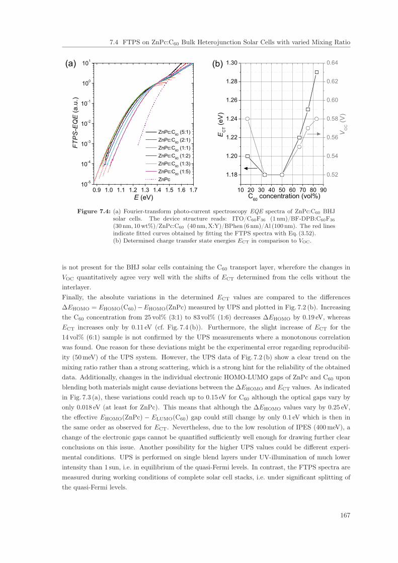
7.4 FTPS on ZnPc:C60 Bulk Heterojunction Solar Cells with varied Mixing Ratio
Figure 7.4: (a) Fourier-transform photo-current spectroscopy EQE spectra of ZnPc:C60 BHJsolar cells. The device structure reads: ITO/C60F36 (1 nm)/BF-DPB:C60F36
(30 nm, 10 wt%)/ZnPc:C60 (40 nm, X:Y)/BPhen (6 nm)/Al (100 nm). The red linesindicate fitted curves obtained by fitting the FTPS spectra with Eq. (3.52).(b) Determined charge transfer state energies ECT in comparison to VOC.
is not present for the BHJ solar cells containing the C60 transport layer, wherefore the changes inVOC quantitatively agree very well with the shifts of ECT determined from the cells without theinterlayer.Finally, the absolute variations in the determined ECT values are compared to the differencesΔEHOMO = EHOMO(C60)−EHOMO(ZnPc) measured by UPS and plotted in Fig. 7.2 (b). Increasingthe C60 concentration from 25 vol% (3:1) to 83 vol% (1:6) decreases ΔEHOMO by 0.19 eV, whereasECT increases only by 0.11 eV (cf. Fig. 7.4 (b)). Furthermore, the slight increase of ECT for the14 vol% (6:1) sample is not confirmed by the UPS measurements where a monotonous correlationwas found. One reason for these deviations might be the experimental error regarding reproducibil-ity (50 meV) of the UPS system. However, the UPS data of Fig. 7.2 (b) show a clear trend on themixing ratio rather than a strong scattering, which is a strong hint for the reliability of the obtaineddata. Additionally, changes in the individual electronic HOMO-LUMO gaps of ZnPc and C60 uponblending both materials might cause deviations between the ΔEHOMO and ECT values. As indicatedin Fig. 7.3 (a), these variations could reach up to 0.15 eV for C60 although the optical gaps vary byonly 0.018 eV (at least for ZnPc). This means that although the ΔEHOMO values vary by 0.25 eV,the effective EHOMO(ZnPc) − ELUMO(C60) gap could still change by only 0.1 eV which is then inthe same order as observed for ECT. Nevertheless, due to the low resolution of IPES (400 meV), achange of the electronic gaps cannot be quantified sufficiently well enough for drawing further clearconclusions on this issue. Another possibility for the higher UPS values could be different experi-mental conditions. UPS is performed on single blend layers under UV-illumination of much lowerintensity than 1 sun, i.e. in equilibrium of the quasi-Fermi levels. In contrast, the FTPS spectra aremeasured during working conditions of complete solar cell stacks, i.e. under significant splitting ofthe quasi-Fermi levels.
167

7 Investigations on ZnPc:C60 Blends
In summary, the observed VOC dependence on the mixing ratio could be clearly attributed to changesin the energy levels of ZnPc and C60 when mixing both materials. This trend is confirmed by UPSand ECT measurements despite of deviations between both methods. Hence, physical reasons forthe observed energy level shifts and changes in ECT will be discussed in the following section.
7.5 Discussion of the Energy Level Variations
Changes of VOC with the blend mixing ratio of the photo-active layer were also published for poly-mer based BHJ solar cells, for which two different explanations have been suggested. [319,321,324]
On the one hand, blending donor and acceptor materials at different ratios could lead to a stabi-lization or destabilization of the CT energy and thus might change the individual energy levels dueto changed polarization screening. Effectively, this can be expressed by a varying blend dielectricconstant εr. For instance, for PF10TBT:PCBM4 BHJ solar cells an increase of VOC from 1.00 V to1.15 V by decreasing the PCBM concentration from 80 to 5wt% was reported. [324] Correspondingly,an increase of ECT by approximately 0.13 eV was found and explained by a decrease of the effectiveblend permittivity from 3.85 (80 wt% PCBM) to 3.4 (1wt% PCBM). [324]
In contrast, the trend in VOC obtained for the ZnPc:C60 BHJ solar cells here is opposite (cf.Fig. 7.1 (b)). Thus, the blend permittivity is estimated by impedance spectroscopy on metal/ZnPc:C60
(d nm)/metal structures in which the blend thickness d is varied.5 Plotting the measured geometriccapacitance of the device versus 1/d yields a linear correlation from which slope the relative per-mittivity εr is fitted. The determined values are summarized in Tab. 7.1. However, the obtainedpermittivities scatter around that of the pure films (ZnPc: 4.0; C60: 5.0), which does not allow aclear correlation with the observed trend in VOC. Interestingly, the permittivity of the pure donor islower than that of the pure acceptor layer in accordance to the system PF10TBT:PCBM, althoughthe VOC dependence on the acceptor concentration is inverse for both systems.The observed energy level shifts might also be caused by morphological changes of the donor and/oracceptor phase due to blending both materials. Piersimoni et al. reported on a reduction of ECT byabout 0.12 eV at high fullerene concentrations in MDMO-PPV:PCBM6 blends which was attributedto an increased phase separation and thus rising amount of PCBM nanoclusters for high fullereneconcentrations. [319] Furthermore, crystallization of the donor phase was reported to alter VOC inP3HT:PCBM7 based solar cells. [321] In particular, increasing the mass fraction of well defined highlycrystalline polymer to total polymer content from 10 to 90 % leads to a decrease of VOC by approx-imately 0.11 V as well as of ECT by 0.11 eV. [321]
The morphology of ZnPc:C60 =1:1 blends was intensively investigated by means of transmission andscanning electron microscopy (TEM, SEM), [27] grazing incidence X-ray diffraction (GIXRD) andvariable angle spectroscopic ellipsometry (VASE), [318] atomic force microscopy (AFM), [27,318] andtransmission X-ray microscopy (TXM). [325] In this context, an already phase-separated structure ofboth, ZnPc and C60 domains, was revealed by means of GIXRD for 1:1 blends evaporated at roomtemperature. [318] However, the crystallite sizes are supposed to be very small (< 10 nm) since the
4poly[2,7-(9,9-dialkylfluorene)-alt-5,5-(4,7-di-2-thienyl-2,1,3-benzothiadiazole)] : [6,6]-phenyl-C61 butyric acidmethyl ester
5The measurements are performed by Lorentzo Burtone at the IAPP.6poly[2-methoxy-5-(30,70-dimethyloctyloxy)-1,4-phenylene vinylene] : [6,6]-phenyl-C61 butyric acid methyl ester7poly(3-hexylthiophene) : [6,6]-phenyl-C61 butyric acid methyl ester
168

7.5 Discussion of the Energy Level Variations
θ
C60 conc. (vol%) rel. permittivity εr
0 4.037 5.054 5.370 4.6100 5.0
Figure 7.5: GIXRD pattern of 150 nmZnPc:C60 blends with varying mixing ratioevaporated at room temperature on glass.The dotted pattern originate from respec-tive pure films.
Table 7.1: Relative permittivities εr ofZnPc:C60 blend layers with varied mix-ing ratios measured by impedance spec-troscopy on metal/blend/metal struc-tures.
full width half maxima of the GIXRD peaks are very broad. Similar findings were published for thesimilar material system CuPc:C60. [326]
GIXRD patterns of 150 nm ZnPc:C60 blends with varied mixing ratio evaporated at room temper-ature on glass are shown in Fig. 7.5.8 Additionally, diffraction pattern of pure ZnPc and C60 layerare plotted to identify the obtained Bragg reflections (dotted lines, cf. Ref. [318]).In comparison to the pure film, slightly broadened ZnPc peaks at 2θ = {7 ◦; 14 ◦} are present for the6:1 blend (gray line). The ZnPc peaks are decreasing in intensity and get broadened by increasingthe fullerene concentration. Additionally, C60 related peaks arise at 2θ = {11 ◦; 18 ◦; 21 ◦}, but arestrongly smeared out in comparison to the pure C60 film pattern. Only at the lowest ZnPc:C60 ratioof 1:6 (black line) distinct Bragg reflections of C60 are visible. Already at a ZnPc:C60 ratio of 1:3the C60 peaks at 2θ = {18 ◦; 21 ◦} are significantly broadened which means that the formation ofC60 crystals is strongly disturbed by the presence of donor molecules. At medium concentrations,the 2θ = 11 ◦ peak vanishes and finally no C60 related peaks are visible for the 6:1 blend (grayline). For ZnPc the situation is different. The peak at 2θ = 7 ◦ is still present even at the highestacceptor concentration, which unambiguously indicates a nano-crystalline ZnPc phase. At mediumconcentrations, this peak is partially superimposed by the extremely broadened C60 features of the2θ = 11 ◦ peak but clearly visible for concentrations above 1:1. Nonetheless, in comparison to thepure ZnPc film, the 2θ = 7 ◦ peak is broadened at any mixing ratio which corresponds to signifi-
8The GIXRD measurements are conducted by Lutz Wilde at the Fraunhofer CNT (Dresden, Germany).
169

7 Investigations on ZnPc:C60 Blends
cantly reduced crystal sizes within the blends. Here, it shall be emphasized that although applyinggrazing incidence XRD, detection of the Bragg reflections is close to the resolution limit for allconcentrations. Analyzing the same samples by usual specular XRD in Bragg-Bretano geometryreveals no features. This finding means that the actual crystal sizes of both materials remain in therange of only a few nanometer. [318]
In summary, the GIXRD data show that the ZnPc phase within the blend is mainly maintainednano-crystalline independent of the mixing ratio, whereas the C60 phase is significantly influenced bythe amount of ZnPc molecules. Here, crystallization is suppressed at high ZnPc amounts and nano-crystallites are only present for fullerene concentrations above 75 vol%. Also by UPS, the strongestshifts of the HOMO-onsets with respect to the Fermi level have been observed for C60 rather thanfor ZnPc (cf. Fig. 7.2 (b)). This comparison suggests a correlation between the morphology of theC60 phase and the corresponding energy levels, e.g. due to different interaction strengths betweenoverlapping molecular orbitals in a nanocrystal or in a more disordered phase. For instance, allC60 related GIXRD peaks have disappeared for the 6:1 sample, i.e. practically there must be anamorphous acceptor phase. Accordingly, the HOMO-onset of C60 is shifted furthest from the ZnPcHOMO-onset at this ratio (cf. Fig. 7.2 (a)). In contrast, an almost nano-crystalline C60 phase couldbe identified for the 1:6 sample for which also the C60 HOMO-onset lies much closer to that ofZnPc. Interestingly, the latter lies approximately 0.8 eV below the Fermi level for all blend ratios,which seems reasonable since also the morphology of the ZnPc phase is not significantly changed atdifferent blend ratios. Hence, it can be concluded by this analogy that the main driving force forthe blend energy level alignment seems to be the crystallization grade of C60 rather than that ofZnPc.
7.6 Substrate Dependence of the Energy Levels of ZnPc and
ZnPc:C60 Blends
Schünemann et al. showed by means of XRD, AFM, and VASE that ZnPc thin-films grow in amode with standing upright molecules on weakly interacting substrates (e.g. glass, amorphous or-ganics) due to π-stacking perpendicular to the substrate, whereas on strongly interacting surfaces(e.g. thermally evaporated gold on glass) the molecules are forced to almost lying flat within thefirst layers. [28] Simultaneously, UPS measurements on 5 nm ZnPc films evaporated either directlyon a (unorientied micro-crystalline) gold foil or on top of an amorphous organic interlayer (e.g.p-doped MeO-TPD) reveal different ionization potentials by more than 0.3 eV. In the first case, anIP of 5.31 eV is measured, in the latter 4.98 eV. This difference must be attributed to the differentorientations of ZnPcIt is also possible to derive an individual IP value of ZnPc from a ZnPc:C60 blend UPS spectrumby setting IP(ZnPc) = Wf + EHOMO(ZnPc) (similarly for C60). Corresponding values are givenin Fig. 7.2 (b) for different blend ratios. Here, with increasing C60 concentration the IP of ZnPcincreases by 0.27 eV (gray triangles), that of C60 by 0.13 eV (black triangles). At a ZnPc:C60 ratioof 1:6 the IP of ZnPc reaches 5.31 eV which is fairly equal to the value observed for an intrinsicZnPc film evaporated on gold. In contrast, for high ZnPc amounts (3:1 sample), IP = 5.04 eV isobtained which is similar to intrinsic ZnPc on top of MeO-TPD. This comparison suggests that
170

7.6 Substrate Dependence of the Energy Levels of ZnPc and ZnPc:C60 Blends
Figure 7.6: Evolution of UPS spectra of incrementally evaporated (a) Au/MeO-TPD:F6-TCNNQ (5 nm, 10 wt%)/ZnPc (5 nm)/ZnPc:C60 (10 nm, 1:6) and (b)Au/ZnPc (8 nm)/ZnPc:C60 (12 nm, 1:6) structures. The HOMO-onsets are markedby colored circles and the ΔEHOMO = EHOMO(C60) − EHOMO(ZnPc) differencesare indicated by black arrows.
ZnPc molecules, or at least clusters of ZnPc molecules, might also orient with preferred directionswithin blends depending on the mixing ratio. In particular at high C60 concentrations, this wouldcorrespond to a growth mode similar to a pure film on gold. On the other hand, the ZnPc domainsshould be almost completely surrounded by C60 molecules due to the small crystal sizes in blends.Therefore, the measured energetics by UPS should represent an average over all possible (interface)orientations without a preferred direction. For further clarification of this issue, an even deeperinsight into the morphology of such donor-acceptor blends on a nanometer scale and the respectiveimpact on the energetic landscape is necessary. Finally, is should be emphasized that for calculationof the individual IPs a common blend layer work-function has been assumed which is reasonabledue to the appearance of distinct HBECs, indicating vacuum-level alignment between both speciesin blend, but not self-evident, because for a flat ZnPc:C60 heterojunction a weak interface dipolewas reported in literature. [132]
Since the thin-film growth of pure ZnPc layers is determined by interactions with the substrate,it might also be possible that the growth of ZnPc nanocrystals in blends with C60 is also influencedby the used gold substrate which further would affect the blend energy level alignment. Thus, itmust be shown that the observed energy level shifts in ZnPc:C60 thin-films evaporated on gold foil(cf. Fig. 7.2) are an actual blend property and not caused by the substrate or the growth mode
171

7 Investigations on ZnPc:C60 Blends
ΔΔ
Figure 7.7: Schematic energy level alignment of (a) Au/MeO-TPD:F6-TCNNQ (5 nm, 10 wt%)/ZnPc (5 nm)/ZnPc:C60 (10 nm, 1:6) and (b)Au/ZnPc (8 nm)/ZnPc:C60 (12 nm, 1:6) structures. Corresponding UPS spectraare shown in Fig. 7.6.
of an underlying ZnPc layer, respectively. For this, 1:6 blends are incrementally evaporated eitheron top of Au/MeO-TPD:F6-TCNNQ (5 nm, 10 wt%)/ZnPc (5 nm) or on Au/ZnPc (8 nm) structuresand measured by UPS. The first stack represents an application of the ZnPc:C60 blend within atypical BHJ solar cell, i.e. on top of a HTL or a ”low IP” ZnPc interlayer. In the latter case, theblend is evaporated on "high IP" ZnPc. A ZnPc:C60 blend ratio of 1:6 is chosen since also thestrongest changes in VOC and ECT are found at highest C60 concentrations. The correspondingspectra are given in Fig. 7.6, in which the individual HOMO-onsets are marked by colored circlesand the ΔEHOMO = EHOMO(C60) − EHOMO(ZnPc) differences are indicated by black arrows. Thededuced level alignments are summarized in Fig. 7.7. In both cases, ΔEHOMO differences of 1.13 eVare measured after a few nanometer blend thicknesses. The same value was also obtained for a 1:6blend evaporated directly on gold (cf. Fig. 7.2), whereas for 6:1 it is close to 1.4 eV. These findingsclearly demonstrate that the observed level changes are independent of the substrate and a generalproperty the ZnPc:C60 BHJ. Nevertheless, directly at the ZnPc/ZnPc:C60 interfaces the alignment isdetermined by the underlying ZnPc film, which results in higher (Fig. 7.7 (a)) or lower (Fig. 7.7 (b))ΔEHOMO values. However, after a few nanometer the bulk properties of the blend are dominatingwhich finally is more important for the achievable VOC of a BHJ solar cell.
7.7 Summary
The dependence of the open-circuit voltage of BHJ solar cells comprising ZnPc:C60 as photo-activeblend on its mixing ratio is studied. Increasing the C60 amount from 25 to 86 vol% leads to alinear increase in VOC by 0.10 V to 0.63 V. This enhancement could be attributed to a respectiveincreased effective donor-acceptor gap at high C60 concentrations. In detail, a change in ΔEHOMO =
EHOMO(C60)−EHOMO(ZnPc) by 0.25 eV upon the stoichiometry variation has been determined byUPS. The observed energy level shifts are detected regardless of the used substrate. Furthermore,FTPS measurements reveal quantitatively the same dependence of the charge transfer state energyECT on the blend mixing ratio as observed for VOC. Interestingly, for polymer based BHJ solar cellsa reversed trend was published, i.e. a decreasing VOC and/or ECT with increasing acceptor (PCBM)amount. [319]
172
7.7 Summary
GIXRD experiments reveal a suppressed crystallization of the C60 phase for ZnPc concentrationsabove 25 vol%. In contrast, an almost undisturbed ZnPc nanocrystal formation could be concludedfrom the diffraction pattern. Therefore, the crystallization degree of the C60 phase is supposed togovern the observed variations in the energy levels at different mixing ratios. For the polymer baseddonor:acceptor blends, changes in the energy levels were also attributed to the crystallinity of thePCBM phase, however, with an inverse dependence on the mixing ratio. [319]
173

7 Investigations on ZnPc:C60 Blends
174

8 | Conclusion and Outlook
8.1 Conclusion
It was the aim of this thesis to improve the understanding of the relative energy level alignment inmixed organic semiconductor thin-films. Here, the focus was on studying molecular doping by em-ploying UV and X-ray photoelectron spectroscopy (UPS/XPS) to various host:dopant systems. Theexperimental findings were explained by a statistical description in order to contribute to the funda-mental understanding of the underlying doping mechanism. Besides, the energy level alignment inblends of ZnPc:C60, representing a prototype donor:acceptor system for organic bulk heterojunctionsolar cells, was studied in detail.
First, the Fermi level positions in thin-films of the common hole transport materials MeO-TPD,ZnPc, and pentacene (P5) p-doped by the acceptor molecules C60F36 and F6-TCNNQ were mea-sured under systematic variation of the doping concentration. The precise control of doping ratiosin a range of MR = 10−5 . . . 1 has been demonstrated and allowed thus for tuning the Fermi levelover the whole semiconductor gap. Therefore, an analysis of the doping properties in a muchbroader range as previously accessible become possible. Material characteristic kinks and slopeswere found in the Fermi level vs. doping concentration plots. Typically, strong shifts of the Fermilevel over several 100 meV at characteristic doping concentrations (MeO-TPD: MR ≈ 2 × 10⁻³,ZnPc: MR ≈ 5 × 10⁻⁴, P5: MR ≈ 4 × 10⁻⁵) were measured and explained by the presence of thedeep trap states, hindering the doping process at low concentrations. At high molar doping ratios,Fermi level pinning a few 100meV above the UPS HOMO-onsets was observed. By numerically solv-ing the charge neutrality equation using a classical semiconductor physics approach, these findingswere explained by trap-limitation, dopant saturation, and reserve regimes as known from inorganicsemiconductor physics. Here, the characteristic pinning energies are attributed to effective accep-tor levels, e.g. EA = 0.46 eV (MeO-TPD:C60F36), EA = 0.41 eV (P5:C60F36), and EA = 0.27 eV
(ZnPc:F6-TCNNQ), which mark the transition from dopant saturation to reserve and cause there-fore kinks in the EF vs. MR plots. Using density of states parameter obtained from fitting highresolution UPS spectra, the measured Fermi level graphs could be reproduced well over five ordersof magnitude in the doping concentration. It was furthermore demonstrated that the density ofdeep gap states depends on the purity degree of the host material, for instance being 6 times higherin unsublimed compared to fourfold purified MeO-TPD. The above findings were confirmed by mea-surements of the doping efficiency, defined as ratio between the density of free holes provided bydoping and incorporated acceptor molecules. The doping efficiencies were estimated from depletion
175

8 Conclusion and Outlook
layer thicknesses at Schottky contacts measured by incremental UPS. For each system, decreasingvalues with increasing doping ratios to just a few percent above MR = 0.1 were found. In particular,measurements on the system ZnPc:F6-TCNNQ strongly indicated doping efficiencies controlled bytrap-limitation, dopant saturation, and reserve regimes.
Similar UPS/IPES studies were conducted on thin-films of C60, ZnPc, and pentacene n-dopedby the di-metal complex W2(hpp)4. In contrast to the p-doping experiments, shifts of the Fermilevel very close to or even above the LUMO-onsets of the host materials were found. In particu-lar, either no kinks (n-P5) or just each one kink (n-ZnPc, n-C60) were observed in the Fermi levelvs. doping concentrations plots, which however, show material characteristic slopes. Applicationof the statistical description yields efficient n-doping, i.e. the measurement curves could be fittedby assuming just dopant saturation and trap-limitation. Here, electron traps with densities in theorder of 1.9 × 1018 cm−3 and 3.4 × 1018 cm−3 are supposed to cause the kinks in the Fermi levelplots of n-doped ZnPc and C60, respectively. Additionally, it could be demonstrated that intentionalelectron traps with a defined density can be introduced in P5 thin-films by co-evaporation with C60
(N0(C60)/N0(P5) � 0.03). These traps are filled up by n-doping when the molar doping ratio ofW2(hpp)4 exceeds the relative density of C60 molecules (3 mol%). At concentrations below, theFermi level is pinned close to its intrinsic position. Finally, the appearance of n-doping related gapstates, which increase in intensity with rising molar doping ratios, could be reported for all threeinvestigated host materials.In contrast to p-dopants, the highly efficient n-dopant W2(hpp)4 is prone to degradation in air dueto its low IP of just 2.4 eV. Therefore, the degradation of pure films of W2(hpp)4 as well as ofn-doped ZnPc, P5, C60, Bis-HFl-NTCDI, and NET108 films was systematically studied under airexposure by conductivity and UPS/XPS measurements. In this context, an unexpected (partial)protection of W2(hpp)4 molecules against oxidation was found within C60, Bis-HFl-NTCDI, andNET108 layers on a time scale of less than one hour. Although the conductivity of n-C60 filmsrapidly drops by orders of magnitude immediately after air exposure, it could be recovered by up to33 % of the initial value by thermal annealing in vacuum after storing the sample 16 minutes in air.Furthermore, doped Bis-HFl-NTCDI and NET108 films are practically n-conductive in air, i.e. theconductivity drops only by approximately 66 % during an air exposure of 30 minutes. These findingsare supported by UPS measurements where a shift of the Fermi level towards the gap mid by only0.06 eV after 10minutes of air exposure was found. The amount of degraded and intact moleculeswas estimated by fitting the W4f peak of W2(hpp)4 measured by XPS as well as by correspondingLDI-TOF-MS experiments. It was found that approximately 50 . . . 80% of the dopants immediatelydegrade within seconds after an air exposure, whereas the remaining intact dopants exponentiallydecay with a time constant of approximately 11minutes. However, the n-doping effects completelyvanish un-restorable in ZnPc and P5 films already after a few seconds of air exposure.The above findings were explained by a down-shift of the W2(hpp)4 energy levels upon charge-transfer to a host material with deeper lying energy levels, i.e. the strength of the passivation effectincreases with the EA of the used host material. Thus, new conclusions on the general relativeenergy level alignment in an arbitrary donor:acceptor system with IP(donor) < EA(acceptor) couldbe drawn by taking also the results of the p-doping studies into account. In particular the formationof a common thin-film Fermi level was suggested to explain the blend energy level alignment by an
176

8.2 Outlook
adjustment of the dopant phase related Fermi level to that of the host phase. Consequently, thedonor HOMO is forced to lie energetically below the acceptor LUMO in equilibrium, which is visibleas gap states in UPS spectra of n-doped films. The relative alignment (distance) of the acceptorLUMO and donor HOMO is finally determined by the efficiency of the whole doping process, i.e. thedegree of charge transfer as well as the averagely charge transfer complex dissociation probability(including re-trapping effects), and can be expressed by the depth of an effective ED or EA level in astatistical description. These hypothesis was finally compared to other doping theories, in particularto an explanation based on the formation of dopant-host hybrid molecules as proposed by the Kochgroup. [15]
In a third part of this thesis, the correlation of the relative energy alignment in ZnPc:C60 thin-filmsof varied mixing ratio, the open-circuit voltage of respective BHJ solar cells comprising ZnPc:C60
as photo-active blends, and the charge transfer complex energies ECT was investigated in detail.Here, an increase in VOC by 0.10 V to 0.63 V was found when varying the ZnPc:C60 blend ratio from6:1 to 1:6. This enhancement could be attributed to a respective increased effective donor-acceptorgap at high C60 concentrations. In detail, a change in ΔEHOMO = EHOMO(C60) − EHOMO(ZnPc)by 0.25 eV upon the stoichiometry variation has been determined by UPS. These energy level shiftswere observed regardless of the used substrate. Furthermore, the same quantitative dependence ofthe CT energy ECT on the blend mixing ratio as observed for VOC could be demonstrated by highresolution FTPS measurements, however, yielding values ≈ 0.6 eV higher than eVOC.Finally, GIXRD experiments were conducted on ZnPc:C60 thin-films, revealing a suppressed crystal-lization of the C60 phase for ZnPc concentrations above 25 vol%. In contrast, an almost undisturbedZnPc nanocrystal formation could be concluded from the GIXRD pattern. Thus, the crystallizationdegree of the C60 phase is supposed to govern the observed variations in the energy levels at differentmixing ratios and therefore the observed improvement in VOC.
8.2 Outlook
The results of this work concerning characterization and explanation of p- and n-doping effects invarious organic thin-films represent a step forward in understanding the fundamentals of the molec-ular doping mechanism. In particular, the statistical description from which the trap-limitation,dopant saturation and reserve regimes have been concluded, as well as the observed passivationeffect, which allowed for new conclusions on the relative energy level alignment of host:dopant sys-tems in general, are steps towards a general doping theory. Also, the studies on the energy levelalignment in ZnPc:C60 blends provide helpful experimental data to answer the important questionwhat the main limiting factors for VOC in organic BHJ solar cells are, in particular with respectto corresponding measured charge transfer complex energies which are typically several 100meVhigher. However, the presented results also provide new issues which are of scientific interest andshall be addressed in future for a further growth of organic electronics.
Concerning the topic of molecular p-doping, the most important question is what physically de-termines the low doping efficiencies, i.e. which factors influence the depth of the effective acceptorlevels. Here, a detailed understanding of both the charge transfer as well as the CT complex disso-
177

8 Conclusion and Outlook
ciation process is required since particularly the latter has been identified to mainly limit the overalldoping efficiency. However, the development of a general model seems to be rather difficult sincethese processes are controlled on a microscopic scale, i.e. by intermolecular orientation of dopantand host molecules, the relative positions and overlap of their HOMO and LUMO levels, and (local)electrostatic interactions whose strength depend on the doping concentration. Therefore, a detailedmicroscopic analysis of at least two material systems in comparison to each other is recommended.Suitable techniques might be conductive AFM or an estimation of the molecular short range orderby evaluation of GIXRD spectra of host:dopant blends as presented in Ref. [34] With knowledge ofthe microscopic properties and processes, a (hopping) transport model should be developed whichtakes the dopant activation process into account and can explain measured (temperature dependent)thin-film conductivities. Furthermore, it must consider the (effective) dependence of the mobility onthe energy μ(E), i.e. the exact contribution of states lying deeper in the gap (exponential tail states).The relative host:dopant energy level alignment could be further analyzed by DFT calculations onvarious material combinations. This would particularly allow for an estimation of the degree ofcharge transfer. Additionally, temperature dependent UPS measurements on various host:dopantsystems at different doping concentrations could be conducted for a direct analysis of the tempera-ture activation of dopant molecules and/or trap states.
In case of n-doping, different future experimental investigations are possible. Due to a lack ofexperimental data, first the doping efficiency of W2(hpp)4 doped into various host materials shouldbe measured, aiming a confirmation of the hypothesis of dopant saturation for this compound. Forcomparison, the Fermi level and doping efficiency studies should be extended to other material sys-tems (dopants), employing UPS or IPES. Here, the appearance of gap states should be analyzed indetail (shape, energetic width). Using an UV monochromator or even synchrotron radiation wouldovercome the problem of secondary line emission and subtraction. Extending the molar dopingratios below 10−4 would further allow for an electron trap analysis in n-doped pentacene. Further-more, studying the impact of (various) intentionally introduced traps on the Fermi level shift andthe doping efficiency measured by UPS would allow for a direct/reliable comparison to respectiveTSC/DLTS1 and/or impedance spectroscopy measurements. Finally, degradation/passivation stud-ies as provided here for W2(hpp)4 should be conducted on other n-dopants in order to confirm thegenerality of the proposed energy level alignment.
Although the internal quantum efficiency of the best performing organic solar cells exceeds 90%,splitting of CT states into free holes and electrons at donor/acceptor interfaces is typically accom-panied by an energy loss which reduces the open-circuit voltage and therefore the power conversionefficiency. [261] In this context, validity of the empirical correlation eVOC = ECT − 0.6 eV has beenverified for various material combinations including ZnPc:C60 as shown in this thesis, however, anexplanation is lacking. Nevertheless, the interface energetics of donor/acceptor systems is a crucialpoint, in particular the energy of the lowest (thermally relaxed) CT state which is supposed to beas delocalized as possible for efficient electron/hole dissociation.Obviously, the situation in host:dopant systems is quite similar, only differing in the relative energylevel alignment of the HOMO/LUMO levels of the involved molecules. This analogy should be used
1thermally stimulated currents/deep level transient spectroscopy
178

8.2 Outlook
for a better understanding of both CT dissociation at donor/acceptor interfaces in solar cells aswell as at host/dopant interfaces in doped layers. On the one hand, the energy level alignment at ahost/dopant interface similar to a FHJ in a solar cell could be investigated by incrementally UPSon a sub-nanometer scale. On the other hand, the level alignment in host:dopant blends similar toan donor:acceptor BHJ should be measured under variation of the blend stoichiometry around 1:1,i.e. in the transition regime between p- and n-doping.
179

8 Conclusion and Outlook
180

9 | Appendix
9.1 LDI-TOF-MS Experiments
The degradation of pure thin-films of the n-dopant W2(hpp)4 under air exposure is studied in Sec. 6.2by laser desorption ionization - time of flight - mass spectroscopy (LDI-TOF-MS). To provide com-parability between the different LDI-TOF-MS measurements, it has to be guaranteed that for eachmeasurement the amount of laser shots is sufficient to completely desorb the organic layer. There-fore, test measurements with different numbers of laser shots are conducted on an Au/W2(hpp)4(4 nm) sample. In Fig. 9.1 (left) the measured W2(hpp)4 peak intensity is plotted versus the numberof shots. Approximately after 12 shots the intensity saturates, i.e. the organic material is completelydesorbed. Therefore, 30 shots were used for the LDI-TOF degradation measurements.The second critical parameter is the laser intensity. Thus, the W2(hpp)4 peak intensity has beenchecked while varying the laser intensity between 60 and 140μJ, which is plotted in Fig. 9.1 (right).A plateau is found for 60 . . . 120μJ. The intensity drop at higher laser intensities can be explainedby fracturing of the W2(hpp)4 molecules. Therefore, a laser intensity of 120μJ is used for thedegradation experiments, maximizing the signal intensity but avoiding fracturing effects.
0 3 6 9 12 15
0.0
0.2
0.4
0.6
0.8
1.0
1.2
1.4
Nor
mal
ized
Inte
nsity
per
sho
t seq
uenc
e (a
.u.)
Cumulative number of shots
A laser intensity of 40 μJ was applied for each measurement
0 20 40 60 80 100 120 140
0.0
0.2
0.4
0.6
0.8
1.0
1.2
30 lasershots were applied at onesample spot to obtain each datapoint
Nor
mal
ized
Inte
nsity
(a.u
.)
Laser intensity [μJ]
Figure 9.1: Calibration data of the LDI-TOF-MS spectrometer. The cumulative number oflaser shots (left) as well as the laser intensity (right), applied to an Au/W2(hpp)4(4 nm) sample, are varied, and the intensity of the W2(hpp)4 peak is analyzed.
181

9 Appendix
9.2 Investigations on p-Doping
The Fermi level shift upon p-doping of pentacene and ZnPc thin-films doped by C60F36 or F6-TCNNQis investigated by UPS in Sec. 5.3. Furthermore, the obtained EF vs. MR plots are explained by astatistical description introduced in Sec. 5.2. Fig. 9.2 summarizes the calculation results in compar-ison to the experimental EF values, assuming DOS parameters determined by fitting UPS spectraof pure pentacene and ZnPc thin-films (cf. Tab. 5.5).
Figure 9.2: Measured Fermi level positions versus the molar doping ratio for the material sys-tems pentacene:C60F36 (a) and ZnPc:F6-TCNNQ (b). The lines are calculated,assuming DOS parameters determined by fitting UPS spectra of pure pentaceneand ZnPc thin-films (cf. Tab. 5.5).
182

9.3 List of important Abbreviations
9.3 List of important Abbreviations
Å Ångström: 1Å = 0.1 nm
a.u. arbitrary unitsBHJ bulk heterojuntionCT charge transferDOS density of statesEA electron affinity(E)GDM (extended) Gaussian disorder modelETL electron transport layerETM electron transport materialEQE external quantum efficiencyFF fill factorFHJ flat heterojunctionFTPS Fourier-transform photocurrent spectroscopyFWHM full width at half maximumGIXRD grazing incidence X-ray diffractionHSA hemispherical analyzerHBEC high binding energy cut-offHIB hole injection barrierHOMO highest occupied molecular orbitalHTL hole transport layerHTM hole transport materialIP ionization potentialLCAO linear combination of atomic orbitalsLDI-TOF-MS laser desorption ionization - time of flight - mass spectroscopyLUMO lowest un-occupied molecular orbitalMIGS metal induced gap statesMO molecular orbitalMR molar (doping) ratioOFET organic field-effect transistorOLED organic light emitting diodeOPV organic photovoltaicsOSC organic solar cellPCE power conversion efficiencyPES photoelectron spectroscopyp-i-n p-doped/intrinsic/n-dopedQCM quartz crystal microbalance
183

9 Appendix
SCL space charge layerUHV ultra high vacuumUPS ultraviolet photoelectron spectroscopyWf work functionWR weight ratioXPS X-ray photoelectron spectroscopy
9.4 List of important Symbols
Å Ångström: 1Å = 0.1 nm
C capacitancecm doping concentration in wt %cn doping concentration in mol %Δ interface dipoleΔV , Vbi built-in potentiale elementary charge (1.602 · 1019 C)EA acceptor levelEB binding energyECT charge transfer (complex) energyEC conduction band edgeED donor levelEF Fermi levelEHBEC high binding cut-off energy (with respect to EF )EHOMO UPS HOMO-onset energy (with respect to EF )Ekin kinetic energyELUMO IPES LUMO-onset energy (with respect to EF )Epass pass energy of the hemispherical analyzerET trap leveleV electron voltEV valence band edgeEvac vacuum levelε dielectric constantε0 vacuum dielectric constant (8.854 · 10−12 F/m)g(E) density of statesh Planck constant (6.626 · 10−34 Js)ηdop doping efficiencyj current densityJSC short-circuit current densitykB Boltzmann constant (8.617 eV/K)LD exciton diffusion lengthλ electron free mean path
184

9.5 List of investigated Materials
m massmol% molar percentμ mobilityn free electron densityN0 effective density of states (molecule density)NA acceptor densityNC effective conduction band densityND donor densityNT trap densityNV effective valence band energyp free hole densityS slope parameters, s1, s2 slit parameter of the HSAσ conductivityT temperatureτ characteristic time constantV voltageVOC open-circuit voltagew depletion layer widthwt% weight percentZ complex impedance
9.5 List of investigated Materials
MeO-TPD N,N,N’,N’-tetrakis(4-methoxyphenyl)-benzidineP5 pentaceneZnPc zinc-phthalocyanineC60 buckminster fullereneBis-HFl-NTCDI N,N-Bis(fluorene-2-yl)-naphthalenetetracarboxylic diimideNET108 Novaled electron transporter 108BF-DPB N,N’-Bis(9,9-dimethyl-fluoren-2-yl)-N,N’-diphenyl-benzidineDi-NPD N,N’-diphenyl-N,N’-bis(4’-[N,N-bis(naphth-1-yl)-amino]-biphenyl-4-yl)-benzidineBPhen 4,7-diphenyl-1,10-phenanthrolineC60F36 fluorinated fullereneF6-TCNNQ 1,3,4,5,7,8-hexafluorotetracyanonaphthoquinodimethaneW2(hpp)4 1,3,4,6,7,8-hexayhydro-2H-pyrimido[1,2-a]pyrimidine
185


Bibliography
[1] J. Bardeen and W. Brattain: The Transistor. A Semi-Conductor Triode. Physical Review74(2), 230 (1948). doi:10.1103/PhysRev.74.230.
[2] J. Hoerni: Method of manufacturing semiconductor devices. Patent: US3025589, FairchildSemiconductor (1962).
[3] J. Hoerni: Semiconductor Device. Patent: US3064167, Fairchild Semiconductor (1962).
[4] X. Huang, W.-C. Lee, C. Kuo, D. Hisamoto, L. Chang, J. Kedzierski, E. Anderson,H. Takeuchi, Y.-K. Choi, K. Asano, V. Subramanian, T.-J. King, J. Bokor, and C. Hu: Sub50-nm FinFET: PMOS. International Electron Devices Meeting 1999. pp. 67–70 (1999). doi:10.1109/IEDM.1999.823848.
[5] C. W. Tang: Two-layer organic photovoltaic cell. Applied Physics Letters 48(2), 183 (1986).doi:10.1063/1.96937.
[6] C. W. Tang and S. A. VanSlyke: Organic electroluminescent diodes. Applied Physics Letters51(12), 913 (1987). doi:10.1063/1.98799.
[7] Heliatek GmbH: Neuer Weltrekord für organische Solarzellen: Heliatek behauptet sich mit 12%Zelleffizienz als Technologieführer. In Press Release, 16. January 2013. Dresden (2013).
[8] S. Reineke, F. Lindner, G. Schwartz, N. Seidler, K. Walzer, B. Lüssem, and K. Leo: Whiteorganic light-emitting diodes with fluorescent tube efficiency. Nature 459(7244), 234 (2009).doi:10.1038/nature08003.
[9] K. Myny, E. V. Veenendaal, G. H. Gelinck, J. Genoe, W. Dehaene, and P. Heremans: An8-Bit, 40-Instructions-Per-Second Organic Microprocessor on Plastic Foil. IEEE Journal ofSolid-State Circuits 47(1), 284 (2012).
[10] J. Blochwitz, T. Fritz, M. Pfeiffer, K. Leo, D. Alloway, P. Lee, and N. Armstrong: Interfaceelectronic structure of organic semiconductors with controlled doping levels. Organic Electron-ics 2(2), 97 (2001). doi:10.1016/S1566-1199(01)00016-7.
[11] S. Olthof, W. Tress, R. Meerheim, B. Lüssem, and K. Leo: Photoelectron spectroscopy study ofsystematically varied doping concentrations in an organic semiconductor layer using a molec-ular p-dopant. Journal of Applied Physics 106(10), 103711 (2009). doi:10.1063/1.3259436.
187

[12] B. Lüssem, M. L. Tietze, H. Kleemann, C. Hossbach, J. W. Bartha, A. Zakhidov, and K. Leo:Doped organic transistors operating in the inversion and depletion regime. Nature communi-cations 4, 2775 (2013). doi:10.1038/ncomms3775.
[13] K. Walzer, B. Männig, M. Pfeiffer, and K. Leo: Highly efficient organic devices based on elec-trically doped transport layers. Chemical Reviews 107(4), 1233 (2007). doi:10.1021/cr050156n.
[14] B. Lüssem, M. Riede, and K. Leo: Doping of organic semiconductors. physica status solidi(a) 210(1), 9 (2013). doi:10.1002/pssa.201228310.
[15] I. Salzmann, G. Heimel, S. Duhm, M. Oehzelt, P. Pingel, B. George, A. Schnegg, K. Lips, R.-P.Blum, A. Vollmer, and N. Koch: Intermolecular Hybridization Governs Molecular ElectricalDoping. Physical Review Letters 108(3), 035502 (2012). doi:10.1103/PhysRevLett.108.035502.
[16] A. Mityashin, Y. Olivier, T. Van Regemorter, C. Rolin, S. Verlaak, N. G. Martinelli,D. Beljonne, J. Cornil, J. Genoe, and P. Heremans: Unraveling the mechanism of molec-ular doping in organic semiconductors. Advanced Materials 24(12), 1535 (2012). doi:10.1002/adma.201104269.
[17] S. Mehraeen, V. Coropceanu, and J.-L. Brédas: Role of band states and trap states in theelectrical properties of organic semiconductors: Hopping versus mobility edge model. PhysicalReview B 87(19), 195209 (2013). doi:10.1103/PhysRevB.87.195209.
[18] J. Reinhold: Quantentheorie der Moleküle. Teubner Studienbücher Chemie, Wiesbaden (1994).
[19] N. Karl: Organic Semiconductors. Festkörperprobleme 14, 261 (1974).
[20] W. Nolting: Grundkurs Theoretische Physik: Quantenmechanik Teil1 Grundlagen. Vieweg &Sohn Verlagsgesellschaft mbH, Braunschweig/Wiesbaden (2000).
[21] R. Schüppel: Photoinduzierte Absorptionsspektroskopie an organischen, photovoltaisch aktivenDonor-Akzeptor-Heteroübergängen. Dissertation, TU Dresden (2007).
[22] R. Fitzner, E. Reinold, A. Mishra, E. Mena-Osteritz, H. Ziehlke, C. Körner, K. Leo, M. Riede,M. Weil, O. Tsaryova, A. Weiß, C. Uhrich, M. Pfeiffer, and P. Bäuerle: Dicyanovinyl-Substituted Oligothiophenes: Structure-Property Relationships and Application in Vacuum-Processed Small Molecule Organic Solar Cells. Advanced Functional Materials 21(5), 897(2011). doi:10.1002/adfm.201001639.
[23] R. Schueppel, K. Schmidt, C. Uhrich, K. Schulze, D. Wynands, J. Brédas, E. Brier, E. Reinold,H.-B. Bu, P. Baeuerle, B. Maennig, M. Pfeiffer, and K. Leo: Optimizing organic photovoltaicsusing tailored heterojunctions: A photoinduced absorption study of oligothiophenes with lowband gaps. Physical Review B 77(8), 085311 (2008). doi:10.1103/PhysRevB.77.085311.
[24] H. Ziehlke, R. Fitzner, C. Koerner, R. Gresser, E. Reinold, P. Bäuerle, K. Leo, and M. K. Riede:Side chain variations on a series of dicyanovinyl-terthiophenes: A photoinduced absorptionstudy. The Journal of Physical Chemistry A 115(30), 8437 (2011). doi:10.1021/jp203420m.
[25] E. Silinsh: Organic Molecular Crystals. Springer-Verlag, Berlin Heidelberg New York (1980).
188

[26] H. Haken and H. C. Wolf: Molekülphysik und Quantenchemie. Springer-Verlag, Berlin Hei-delberg New York, 5. edition (2006).
[27] S. Pfuetzner, C. Mickel, J. Jankowski, M. Hein, J. Meiss, C. Schuenemann, C. Elschner, A. A.Levin, B. Rellinghaus, K. Leo, and M. Riede: The influence of substrate heating on morphologyand layer growth in C60:ZnPc bulk heterojunction solar cells. Organic Electronics 12(3), 435(2011). doi:10.1016/j.orgel.2010.12.007.
[28] C. Schünemann, D. Wynands, K.-J. Eichhorn, M. Stamm, K. Leo, and M. Riede: Evaluationand Control of the Orientation of Small Molecules for Strongly Absorbing Organic Thin Films.The Journal of Physical Chemistry C 117(22), 11600 (2013). doi:10.1021/jp400604j.
[29] S. Yim, S. Heutz, and T. Jones: Influence of intermolecular interactions on the structureof phthalocyanine layers in molecular thin film heterostructures. Physical Review B 67(16),165308 (2003). doi:10.1103/PhysRevB.67.165308.
[30] R. C. Haddon, X. Chi, M. E. Itkis, J. E. Anthony, D. L. Eaton, T. Siegrist, C. C. Mattheus,and T. T. M. Palstra: Band Electronic Structure of One- and Two-Dimensional PentaceneMolecular Crystals. The Journal of Physical Chemistry B 106(33), 8288 (2002). doi:10.1021/jp0207937.
[31] C. C. Mattheus, G. A. de Wijs, R. A. de Groot, and T. T. M. Palstra: Modeling the poly-morphism of pentacene. Journal of the American Chemical Society 125(20), 6323 (2003).doi:10.1021/ja0211499.
[32] F. Iwatsu: Size effects on the alpha-beta transformation of phthalocyanine crystals. The Jour-nal of Physical Chemistry 92(6), 1678 (1988). doi:10.1021/j100317a057.
[33] C. Schünemann: Organic Small Molecules: Correlation between Molecular Structure, ThinFilm Growth, and Solar Cell Performance. Dissertation, TU Dresden (2012).
[34] C. Elschner: Structural Investigations of Disordered Organic Thin Films. Dissertation, TUDresden (2013).
[35] R. G. Della Valle, A. Brillante, E. Venuti, L. Farina, A. Girlando, and M. Massino: Exploringthe polymorphism of crystalline pentacene. Organic Electronics 5(1-3), 1 (2004). doi:10.1016/j.orgel.2003.08.017.
[36] C. Elschner, A. A. Levin, L. Wilde, J. Grenzer, C. Schroer, K. Leo, and M. Riede: Determiningthe C60 molecular arrangement in thin films by means of X-ray diffraction. Journal of AppliedCrystallography 44(5), 983 (2011). doi:10.1107/S002188981103531X.
[37] D. Wynands, M. Erber, R. Rentenberger, M. Levichkova, K. Walzer, K.-J. Eichhorn, andM. Stamm: Spectroscopic ellipsometry characterization of vacuum-deposited organic films forthe application in organic solar cells. Organic Electronics 13(5), 885 (2012). doi:10.1016/j.orgel.2012.01.036.
[38] M. L. Tietze, W. Tress, S. Pfützner, C. Schünemann, L. Burtone, M. Riede, K. Leo, K. Van-dewal, S. Olthof, P. Schulz, and A. Kahn: Correlation of open-circuit voltage and energy levels
189

in zinc-phthalocyanine: C60 bulk heterojunction solar cells with varied mixing ratio. PhysicalReview B 88(8), 085119 (2013). doi:10.1103/PhysRevB.88.085119.
[39] M. Schrader, R. Fitzner, M. Hein, C. Elschner, B. Baumeier, K. Leo, M. Riede, P. Bäuerle,and D. Andrienko: Comparative study of microscopic charge dynamics in crystalline acceptor-substituted oligothiophenes. Journal of the American Chemical Society 134(13), 6052 (2012).doi:10.1021/ja300851q.
[40] M. Schrader, C. Körner, C. Elschner, and D. Andrienko: Charge transport in amorphous andsmectic mesophases of dicyanovinyl-substituted oligothiophenes. Journal of Materials Chem-istry 22(41), 22258 (2012). doi:10.1039/c2jm34837c.
[41] D. R. Zahn, G. N. Gavrila, and M. Gorgoi: The transport gap of organic semiconductorsstudied using the combination of direct and inverse photoemission. Chemical Physics 325(1),99 (2006). doi:10.1016/j.chemphys.2006.02.003.
[42] N. Sato, K. Seki, and H. Inokuchi: Polarization energies of organic solids determined byultraviolet photoelectron spectroscopy. Journal of the Chemical Society, Faraday Transactions2 77(9), 1621 (1981). doi:10.1039/f29817701621.
[43] A. Köhler and H. Bässler: What controls triplet exciton transfer in organic semiconductors?Journal of Materials Chemistry 21(12), 4003 (2011). doi:10.1039/c0jm02886j.
[44] R. Noriega, J. Rivnay, K. Vandewal, F. P. V. Koch, N. Stingelin, P. Smith, M. F. Toney,and A. Salleo: A general relationship between disorder, aggregation and charge transport inconjugated polymers. Nature Materials 12(8), 1 (2013). doi:10.1038/nmat3722.
[45] V. Coropceanu, J. Cornil, D. A. da Silva Filho, Y. Olivier, R. Silbey, and J.-L. Brédas:Charge transport in organic semiconductors. Chemical Reviews 107(4), 926 (2007). doi:10.1021/cr050140x.
[46] A. Troisi: Charge transport in high mobility molecular semiconductors: classical models andnew theories. Chemical Society Reviews 40(5), 2347 (2011). doi:10.1039/c0cs00198h.
[47] S. Fratini and S. Ciuchi: Bandlike Motion and Mobility Saturation in Organic MolecularSemiconductors. Physical Review Letters 103(26), 266601 (2009). doi:10.1103/PhysRevLett.103.266601.
[48] T. Sakanoue and H. Sirringhaus: Band-like temperature dependence of mobility in a solution-processed organic semiconductor. Nature Materials 9(9), 736 (2010). doi:10.1038/nmat2825.
[49] M. Mas-Torrent, P. Hadley, S. T. Bromley, X. Ribas, J. Tarrés, M. Mas, E. Molins, J. Ve-ciana, and C. Rovira: Correlation between crystal structure and mobility in organic field-effecttransistors based on single crystals of tetrathiafulvalene derivatives. Journal of the AmericanChemical Society 126(27), 8546 (2004). doi:10.1021/ja048342i.
[50] J. Y. Lee, S. Roth, and Y. W. Park: Anisotropic field effect mobility in single crystal pentacene.Applied Physics Letters 88(25), 252106 (2006). doi:10.1063/1.2216400.
190
[51] A. Chowdhury, B. Biswas, and B. Mallik: Effects of Substrate on the Asymmetric GrainGrowth and Observation of Conductivity Anisotropy in Nanostructured Organic Thin Films.Science of Advanced Materials 5(9), 1297 (2013). doi:10.1166/sam.2013.1586.
[52] N. Tessler, Y. Preezant, N. Rappaport, and Y. Roichman: Charge Transport in DisorderedOrganic Materials and Its Relevance to Thin-Film Devices: A Tutorial Review. AdvancedMaterials 21(27), 2741 (2009). doi:10.1002/adma.200803541.
[53] M. Schwörer and H. C. Wolf: Organische Molekulare Festkörper. WILEY-VCH Verlag, Wein-heim (2005).
[54] N. W. Ashcroft and D. N. Mermin: Solid State Physics. Cengage Learning Emea, Belmont(2010).
[55] K. Bolotin, K. Sikes, Z. Jiang, M. Klima, G. Fudenberg, J. Hone, P. Kim, and H. Stormer:Ultrahigh electron mobility in suspended graphene. Solid State Communications 146(9-10),351 (2008). doi:10.1016/j.ssc.2008.02.024.
[56] V. Umansky, M. Heiblum, Y. Levinson, J. Smet, J. Nübler, and M. Dolev: MBE growth ofultra-low disorder 2DEG with mobility exceeding 35x10ˆ6 cmˆ2/Vs. Journal of Crystal Growth311(7), 1658 (2009). doi:10.1016/j.jcrysgro.2008.09.151.
[57] S. M. Sze: Physics of Semiconductor Devices. John Wiley and Sons, New York, 2. edition(1981).
[58] O. D. Jurchescu, M. Popinciuc, B. J. van Wees, and T. T. M. Palstra: Interface-Controlled,High-Mobility Organic Transistors. Advanced Materials 19(5), 688 (2007). doi:10.1002/adma.200600929.
[59] E. Menard, V. Podzorov, S.-H. Hur, A. Gaur, M. E. Gershenson, and J. A. Rogers: High-Performance n- and p-Type Single-Crystal Organic Transistors with Free-Space Gate Di-electrics. Advanced Materials 16(23-24), 2097 (2004). doi:10.1002/adma.200401017.
[60] J. Mei, Y. Diao, A. L. Appleton, L. Fang, and Z. Bao: Integrated materials design of organicsemiconductors for field-effect transistors. Journal of the American Chemical Society 135(18),6724 (2013). doi:10.1021/ja400881n.
[61] R. W. I. de Boer, M. E. Gershenson, A. F. Morpurgo, and V. Podzorov: Organic single-crystal field-effect transistors. Physica Status Solidi (a) 201(6), 1302 (2004). doi:10.1002/pssa.200404336.
[62] V. C. Sundar, J. Zaumseil, V. Podzorov, E. Menard, R. L. Willett, T. Someya, M. E. Gershen-son, and J. A. Rogers: Elastomeric transistor stamps: reversible probing of charge transportin organic crystals. Science 303(5664), 1644 (2004). doi:10.1126/science.1094196.
[63] C. Reese and Z. Bao: High-Resolution Measurement of the Anisotropy of Charge Transport inSingle Crystals. Advanced Materials 19(24), 4535 (2007). doi:10.1002/adma.200701139.
[64] K. P. Pernstich, B. Rössner, and B. Batlogg: Field-effect-modulated Seebeck coefficient inorganic semiconductors. Nature Materials 7(4), 321 (2008). doi:10.1038/nmat2120.
191
[65] F. Ortmann, F. Bechstedt, and K. Hannewald: Charge transport in organic crystals: interplayof band transport, hopping and electron-phonon scattering. New Journal of Physics 12(2),023011 (2010). doi:10.1088/1367-2630/12/2/023011.
[66] K. Marumoto, S.-i. Kuroda, T. Takenobu, and Y. Iwasa: Spatial Extent of Wave Functionsof Gate-Induced Hole Carriers in Pentacene Field-Effect Devices as Investigated by ElectronSpin Resonance. Physical Review Letters 97(25), 256603 (2006). doi:10.1103/PhysRevLett.97.256603.
[67] M. Pope and C. E. Swenberg: Electronic Processes in Organic Crystals. Oxford UniversityPress, Oxford (1982).
[68] T. Holstein: Studies of Polaron Motion. Annals of Physics 8(3), 325 (1959). doi:10.1016/0003-4916(59)90002-8.
[69] T. Holstein: Studies of Polaron Motion. Annals of Physics 8(3), 343 (1959). doi:10.1006/aphy.2000.6021.
[70] F. Ortmann, F. Bechstedt, and K. Hannewald: Theory of charge transport in organic crystals:Beyond Holstein’s small-polaron model. Physical Review B 79(23), 235206 (2009). doi:10.1103/PhysRevB.79.235206.
[71] K. Hannewald, V. Stojanović, J. Schellekens, P. Bobbert, G. Kresse, and J. Hafner: Theory ofpolaron bandwidth narrowing in organic molecular crystals. Physical Review B 69(7), 075211(2004). doi:10.1103/PhysRevB.69.075211.
[72] N. Koch, A. Vollmer, I. Salzmann, B. Nickel, H. Weiss, and J. Rabe: Evidence for Temperature-Dependent Electron Band Dispersion in Pentacene. Physical Review Letters 96(15), 156803(2006). doi:10.1103/PhysRevLett.96.156803.
[73] W. D. Gill: Drift mobilities in amorphous charge-transfer complexes of trinitrofluorenone andpoly-n-vinylcarbazole. Journal of Applied Physics 43(12), 5033 (1972). doi:10.1063/1.1661065.
[74] A. Miller and E. Abrahams: Impurity Conduction at Low Concentrations. Physical Review120(3), 745 (1960). doi:10.1103/PhysRev.120.745.
[75] N. Mott and W. Twose: The theory of impurity conduction. Advances in Physics 10(38), 107(1961). doi:10.1080/00018736100101271.
[76] S. Novikov, D. Dunlap, V. Kenkre, P. Parris, and A. Vannikov: Essential Role of Correlationsin Governing Charge Transport in Disordered Organic Materials. Physical Review Letters81(20), 4472 (1998). doi:10.1103/PhysRevLett.81.4472.
[77] V. Ambegaokar, B. Halperin, and J. Langer: Hopping Conductivity in Disordered Systems.Physical Review B 4(8), 2612 (1971). doi:10.1103/PhysRevB.4.2612.
[78] M. Sahimi: Applications of Percolation Theory. Taylor and Francis Books, Inc., London(1994).
192

[79] N. F. Mott: Conduction in non-crystalline materials. Philosophical Magazine 19(160), 835(1969). doi:10.1080/14786436908216338.
[80] N. Mott and E. Davis: Electronic Processes in Non- crystalline Materials. Clarendon Press,Oxford (1979).
[81] M. C. J. M. Vissenberg and M. Matters: Theory of the field-effect mobility in amorphousorganic transistors. Physical Review B 57(20), 12964 (1998). doi:10.1103/PhysRevB.57.12964.
[82] H. Bässler: Charge Transport in Disordered Organic Photoconductors a Monte Carlo Simula-tion Study. physica status solidi (b) 175(1), 15 (1993). doi:10.1002/pssb.2221750102.
[83] C. C. Mattheus, A. B. Dros, J. Baas, G. T. Oostergetel, A. Meetsma, J. L. de Boer, andT. T. Palstra: Identification of polymorphs of pentacene. Synthetic Metals 138(3), 475 (2003).doi:10.1016/S0379-6779(02)00467-8.
[84] C. Schünemann, C. Elschner, A. Levin, M. Levichkova, K. Leo, and M. Riede: Zinc ph-thalocyanine - Influence of substrate temperature, film thickness, and kind of substrate on themorphology. Thin Solid Films 519(11), 3939 (2011). doi:10.1016/j.tsf.2011.01.356.
[85] Y. Gartstein and E. Conwell: High-field hopping mobility in molecular systems with spatiallycorrelated energetic disorder. Chemical Physics Letters 245(4-5), 351 (1995). doi:10.1016/0009-2614(95)01031-4.
[86] C. Tanase, E. J. Meijer, P. W. M. Blom, and D. M. de Leeuw: Unification of the HoleTransport in Polymeric Field-Effect Transistors and Light-Emitting Diodes. Physical ReviewLetters 91(21), 216601 (2003). doi:10.1103/PhysRevLett.91.216601.
[87] C. Tanase, P. Blom, and D. de Leeuw: Origin of the enhanced space-charge-limited current inpoly(p-phenylene vinylene). Physical Review B 70(19), 193202 (2004). doi:10.1103/PhysRevB.70.193202.
[88] W. Pasveer, J. Cottaar, C. Tanase, R. Coehoorn, P. Bobbert, P. Blom, D. de Leeuw, andM. Michels: Unified Description of Charge-Carrier Mobilities in Disordered Semiconduct-ing Polymers. Physical Review Letters 94(20), 206601 (2005). doi:10.1103/PhysRevLett.94.206601.
[89] R. Coehoorn, W. Pasveer, P. Bobbert, and M. Michels: Charge-carrier concentration depen-dence of the hopping mobility in organic materials with Gaussian disorder. Physical ReviewB 72(15), 155206 (2005). doi:10.1103/PhysRevB.72.155206.
[90] R. Coehoorn and S. van Mensfoort: Effects of disorder on the current density and recom-bination profile in organic light-emitting diodes. Physical Review B 80(8), 085302 (2009).doi:10.1103/PhysRevB.80.085302.
[91] M. Bouhassoune, S. L. M. van Mensfoort, P. A. Bobbert, and R. Coehoorn: Carrier-densityand field-dependent charge-carrier mobility in organic semiconductors with correlated Gaussiandisorder. Organic Electronics 10(3), 437 (2009). doi:10.1016/j.orgel.2009.01.005.
193

[92] U. Gómez, M. Leonhardt, H. Port, and H. Wolf: Optical properties of amorphous ultrathinfilms of perylene derivatives. Chemical Physics Letters 268(1-2), 1 (1997). doi:10.1016/S0009-2614(97)00184-X.
[93] M. El-Nahass, H. Zeyada, M. Aziz, and N. El-Ghamaz: Structural and optical properties ofthermally evaporated zinc phthalocyanine thin films. Optical Materials 27(3), 491 (2004).doi:10.1016/j.optmat.2004.04.010.
[94] C. Körner: Oligothiophene Materials for Organic Solar Cells - Photophysics and Device Prop-erties. Dissertation, TU Dresden (2012).
[95] O. Gordan, M. Friedrich, and D. Zahn: The anisotropic dielectric function for copper phthalo-cyanine thin films. Organic Electronics 5(6), 291 (2004). doi:10.1016/j.orgel.2004.10.001.
[96] P. I. Djurovich, E. I. Mayo, S. R. Forrest, and M. E. Thompson: Measurement of the lowest un-occupied molecular orbital energies of molecular organic semiconductors. Organic Electronics10(3), 515 (2009). doi:10.1016/j.orgel.2008.12.011.
[97] S. Krause, M. B. Casu, A. Schöll, and E. Umbach: Determination of transport levels oforganic semiconductors by UPS and IPS. New Journal of Physics 10(8), 085001 (2008). doi:10.1088/1367-2630/10/8/085001.
[98] D. L. Dexter: A Theory of Sensitized Luminescence in Solids. The Journal of Chemical Physics21(5), 836 (1953). doi:10.1063/1.1699044.
[99] T. Förster: Zwischenmolekulare Energiewanderung und Fluoreszenz. Annalen der Physik 2(1-2), 55 (1948).
[100] R. C. Powell and Z. G. Soos: Singlet exciton energy transfer in organic solids. Journal ofLuminescence 11(1-2), 1 (1975). doi:10.1016/0022-2313(75)90077-0.
[101] P. Peumans, S. Uchida, and S. R. Forrest: Efficient bulk heterojunction photovoltaic cellsusing small-molecular-weight organic thin films. Nature 425(6954), 158 (2003). doi:10.1038/nature01949.
[102] R. R. Lunt, N. C. Giebink, A. A. Belak, J. B. Benziger, and S. R. Forrest: Exciton diffusionlengths of organic semiconductor thin films measured by spectrally resolved photoluminescencequenching. Journal of Applied Physics 105(5), 053711 (2009). doi:10.1063/1.3079797.
[103] R. R. Lunt, J. B. Benziger, and S. R. Forrest: Relationship between crystalline order andexciton diffusion length in molecular organic semiconductors. Advanced Materials 22(11),1233 (2010). doi:10.1002/adma.200902827.
[104] N. Koch, A. Kahn, J. Ghijsen, J.-J. Pireaux, J. Schwartz, R. L. Johnson, and A. Elschner:Conjugated organic molecules on metal versus polymer electrodes: Demonstration of a keyenergy level alignment mechanism. Applied Physics Letters 82(1), 70 (2003). doi:10.1063/1.1532102.
194

[105] H. Ishii, K. Sugiyama, E. Ito, and K. Seki: Energy Level Alignment and Interfacial ElectronicStructures at Organic/Metal and Organic/Organic Interfaces. Advanced Materials 11(8), 605(1999). doi:10.1002/(SICI)1521-4095(199906)11:8<605::AID-ADMA605>3.0.CO;2-Q.
[106] N. Hayashi, H. Ishii, Y. Ouchi, and K. Seki: Examination of band bending at buckminster-fullerene C60/metal interfaces by the Kelvin probe method. Journal of Applied Physics 92(7),3784 (2002). doi:10.1063/1.1504495.
[107] A. Kahn, N. Koch, and W. Gao: Electronic structure and electrical properties of interfacesbetween metals and pi-conjugated molecular films. Journal of Polymer Science Part B: PolymerPhysics 41(21), 2529 (2003). doi:10.1002/polb.10642.
[108] J. Hwang, A. Wan, and A. Kahn: Energetics of metal-organic interfaces: New experimentsand assessment of the field. Materials Science and Engineering R 64(1-2), 1 (2009). doi:10.1016/j.mser.2008.12.001.
[109] S. Braun, W. R. Salaneck, and M. Fahlman: Energy-Level Alignment at Organic/Metal andOrganic/Organic Interfaces. Advanced Materials 21(14-15), 1450 (2009). doi:10.1002/adma.200802893.
[110] I. Hill, D. Milliron, J. Schwartz, and A. Kahn: Organic semiconductor interfaces: electronicstructure and transport properties. Applied Surface Science 166(1-4), 354 (2000). doi:10.1016/S0169-4332(00)00449-9.
[111] N. Koch: Organic electronic devices and their functional interfaces. ChemPhysChem: AEuropean Journal of Chemical Physics and Physical Chemistry 8(10), 1438 (2007). doi:10.1002/cphc.200700177.
[112] M. Grobosch and M. Knupfer: Charge-Injection Barriers at Realistic Metal/Organic Inter-faces: Metals Become Faceless. Advanced Materials 19(5), 754 (2007). doi:10.1002/adma.200602435.
[113] C. Tengstedt, W. Osikowicz, W. R. Salaneck, I. D. Parker, C.-H. Hsu, and M. Fahlman:Fermi-level pinning at conjugated polymer interfaces. Applied Physics Letters 88(5), 053502(2006). doi:10.1063/1.2168515.
[114] J. Hwang, E.-G. Kim, J. Liu, J.-L. Bredas, A. Duggal, and A. Kahn: Photoelectron Spec-troscopic Study of the Electronic Band Structure of Polyfluorene and Fluorene-ArylamineCopolymers at Interfaces. Journal of Physical Chemistry C 111(3), 1378 (2007). doi:10.1021/jp067004w.
[115] P. S. Davids, A. Saxena, and D. L. Smith: Nondegenerate continuum model for polymer light-emitting diodes. Journal of Applied Physics 78(6), 4244 (1995). doi:10.1063/1.359886.
[116] P. S. Davids, A. Saxena, and D. L. Smith: Bipolaron lattice formation at metal-polymerinterfaces. Physical Review B 53(8), 4823 (1996). doi:10.1103/PhysRevB.53.4823.
[117] E. Tsiper, Z. Soos, W. Gao, and A. Kahn: Electronic polarization at surfaces and thin filmsof organic molecular crystals: PTCDA. Chemical Physics Letters 360(1-2), 47 (2002). doi:10.1016/S0009-2614(02)00774-1.
195

[118] P. Y. Yu and M. Cardona: Fundamentals of Semiconductors. Springer-Verlag, HeidelbergDordrecht London New York, 4. edition (2010).
[119] A. Wan, J. Hwang, F. Amy, and A. Kahn: Impact of electrode contamination on the α-NPD/Au hole injection barrier. Organic Electronics 6(1), 47 (2005). doi:10.1016/j.orgel.2005.02.003.
[120] C. Shen, I. G. Hill, A. Kahn, and J. Schwartz: Organometallic Chemistry at theMagnesium/Tris(8-hydroxyquinolino)aluminum Interface. Journal of the American Chemi-cal Society 122(22), 5391 (2000). doi:10.1021/ja994265t.
[121] C. Shen and A. Kahn: The role of interface states in controlling the electronic structure ofAlq3/reactive metal contacts. Organic Electronics 2(2), 89 (2001). doi:10.1016/S1566-1199(01)00015-5.
[122] C. Shen, A. Kahn, and J. Schwartz: Chemical and electrical properties of interfaces be-tween magnesium and aluminum and tris-(8-hydroxy quinoline) aluminum. Journal of AppliedPhysics 89(1), 449 (2001). doi:10.1063/1.1333740.
[123] H. Vázquez, F. Flores, R. Oszwaldowski, J. Ortega, R. Pérez, and A. Kahn: Barrier formationat metal-organic interfaces: dipole formation and the charge neutrality level. Applied SurfaceScience 234(1-4), 107 (2004). doi:10.1016/j.apsusc.2004.05.084.
[124] H. Vázquez, R. Oszwaldowski, P. Pou, J. Ortega, R. Pérez, F. Flores, and A. Kahn: Dipoleformation at metal/PTCDA interfaces: Role of the Charge Neutrality Level. EurophysicsLetters (EPL) 65(6), 802 (2004). doi:10.1209/epl/i2003-10131-2.
[125] F. Flores and C. Tejedor: On the formation of semiconductor interfaces. Journal of PhysicsC: Solid State Physics 20(2), 145 (1987). doi:10.1088/0022-3719/20/2/001.
[126] W. Mönch: Metal-semiconductor contacts: electronic properties. Surface Science 299-300(1),928 (1994). doi:10.1016/0039-6028(94)90707-2.
[127] I. G. Hill and A. Kahn: Energy level alignment at interfaces of organic semiconductor het-erostructures. Journal of Applied Physics 84(10), 5583 (1998). doi:10.1063/1.368864.
[128] I. G. Hill and A. Kahn: Organic semiconductor heterointerfaces containing bathocuproine.Journal of Applied Physics 86(8), 4515 (1999). doi:10.1063/1.371395.
[129] I. Salzmann, S. Duhm, G. Heimel, M. Oehzelt, R. Kniprath, R. L. Johnson, J. P. Rabe,and N. Koch: Tuning the ionization energy of organic semiconductor films: the role of in-tramolecular polar bonds. Journal of the American Chemical Society 130(39), 12870 (2008).doi:10.1021/ja804793a.
[130] F. J. Zhang, A. Vollmer, J. Zhang, Z. Xu, J. P. Rabe, and N. Koch: Energy level alignment andmorphology of interfaces between molecular and polymeric organic semiconductors. OrganicElectronics 8(5), 606 (2007). doi:10.1016/j.orgel.2007.04.010.
196

[131] R. J. Murdey and W. R. Salaneck: Charge Injection Barrier Heights Across Multilayer OrganicThin Films. Japanese Journal of Applied Physics 44(6A), 3751 (2005). doi:10.1143/JJAP.44.3751.
[132] S. H. Park, J. G. Jeong, H.-J. Kim, S.-H. Park, M.-H. Cho, S. W. Cho, Y. Yi, M. Y. Heo,and H. Sohn: The electronic structure of C60/ZnPc interface for organic photovoltaic devicewith blended layer architecture. Applied Physics Letters 96(1), 013302 (2010). doi:10.1063/1.3285174.
[133] J. X. Tang, C. S. Lee, and S. T. Lee: Electronic structures of organic/organic heterojunctions:From vacuum level alignment to Fermi level pinning. Journal of Applied Physics 101(6),064504 (2007). doi:10.1063/1.2710297.
[134] J. X. Tang, K. M. Lau, C. S. Lee, and S. T. Lee: Substrate effects on the electronic propertiesof an organic/organic heterojunction. Applied Physics Letters 88(23), 232103 (2006). doi:10.1063/1.2209212.
[135] H. Vázquez, W. Gao, F. Flores, and A. Kahn: Energy level alignment at organic hetero-junctions: Role of the charge neutrality level. Physical Review B 71(4), 041306 (2005). doi:10.1103/PhysRevB.71.041306.
[136] F. Löser, M. L. Tietze, B. Lüssem, and J. Blochwitz-Nimoth: Chapter 9: Conductivity Doping.In Fundamentals of High-Efficiency OLEDs: Basic Science to Manufacturing of Organic Light-Emitting Diodes, edited by D. J. Gaspar and E. Polikarpov. Taylor and Francis Books, Inc.,1. edition (2013).
[137] J. Tardy, M. B. Khalifa, and D. Vaufrey: Organic light emitting devices with doped electrontransport and hole blocking layers. Materials Science and Engineering: C 26(2-3), 196 (2006).doi:10.1016/j.msec.2005.10.061.
[138] S. Watanabe, N. Ide, and J. Kido: High-Efficiency Green Phosphorescent Organic Light-Emitting Devices with Chemically Doped Layers. Japanese Journal of Applied Physics 46(3A),1186 (2007). doi:10.1143/JJAP.46.1186.
[139] T. Kugler, W. Salaneck, H. Rost, and A. Holmes: Polymer band alignment at the interface withindium tin oxide: consequences for light emitting devices. Chemical Physics Letters 310(5-6),391 (1999). doi:10.1016/S0009-2614(99)00824-6.
[140] S. Olthof, S. Mehraeen, S. K. Mohapatra, S. Barlow, V. Coropceanu, J.-L. Brédas, S. R.Marder, and A. Kahn: Ultralow Doping in Organic Semiconductors: Evidence of Trap Filling.Physical Review Letters 109(17), 176601 (2012). doi:10.1103/PhysRevLett.109.176601.
[141] M. L. Tietze, K. Leo, and B. Lüssem: Quantification of deep hole-trap filling by molecularp-doping: Dependence on the host material purity. Organic Electronics 14(9), 2348 (2013).doi:10.1016/j.orgel.2013.05.036.
[142] Y. Yamamoto, K. Yoshino, and Y. Inuishi: Electrical Properties of Phthalocyanine-HalogenComplexes. Journal of the Physical Society of Japan 47(6), 1887 (1979). doi:10.1143/JPSJ.47.1887.
197
[143] D. R. Kearns, G. Tollin, and M. Calvin: Electrical Properties of Organic Solids. II. Effectsof Added Electron Acceptor on Metal-Free Phthalocyanine. The Journal of Chemical Physics32(4), 1020 (1960). doi:10.1063/1.1730844.
[144] B. Boudjema, N. El-Khatib, M. Gamoudi, G. Guillaud, and M. Maitrot: Thermally stimulatedcurrents in undoped and doped zinc phthalocyanine films. Revue de Physique Appliquée 23(6),1127 (1988). doi:10.1051/rphysap:019880023060112700.
[145] T. J. Marks: Electrically conductive metallomacrocyclic assemblies. Science 227(4689), 881(1985). doi:10.1126/science.227.4689.881.
[146] M. Maitrot, G. Guillaud, B. Boudjema, J. J. Andre, and J. Simon: Molecular material-basedjunctions: Formation of a Schottky contact with metallophthalocyanine thin films doped by thecosublimation method. Journal of Applied Physics 60(7), 2396 (1986). doi:10.1063/1.337151.
[147] N. El-Khatib, B. Boudjema, G. Guillaud, M. Maitrot, and H. Chermette: Theoretical andexperimental doping of molecular materials: P and N doping of zinc phthalocyanine. Journalof the Less Common Metals 143(1-2), 101 (1988). doi:10.1016/0022-5088(88)90035-5.
[148] E. Lous, P. Blom, L. Molenkamp, and D. Leeuw: Schottky contacts on a highly doped organicsemiconductor. Physical Review B 51(23), 17251 (1995). doi:10.1103/PhysRevB.51.17251.
[149] S. Hiller, D. Schlettwein, N. R. Armstrong, and D. Wöhrle: Influence of surface reactions andionization gradients on junction properties of F16PcZn. Journal of Materials Chemistry 8(4),945 (1998). doi:10.1039/a707485i.
[150] M.-T. Hsieh, C.-C. Chang, J.-F. Chen, and C. H. Chen: Study of hole concentration of1,4-bis[N-(1-naphthyl)-N’-phenylamino]-4,4’ diamine doped with tungsten oxide by admittancespectroscopy. Applied Physics Letters 89(10), 103510 (2006). doi:10.1063/1.2345610.
[151] C.-C. Chang, M.-T. Hsieh, J.-F. Chen, S.-W. Hwang, and C. H. Chen: Highly power efficientorganic light-emitting diodes with a p-doping layer. Applied Physics Letters 89(25), 253504(2006). doi:10.1063/1.2405856.
[152] D.-S. Leem, H.-D. Park, J.-W. Kang, J.-H. Lee, J. W. Kim, and J.-J. Kim: Low driving voltageand high stability organic light-emitting diodes with rhenium oxide-doped hole transportinglayer. Applied Physics Letters 91(1), 011113 (2007). doi:10.1063/1.2754635.
[153] R. Krause, F. Steinbacher, G. Schmidt, J. Hauke Wemken, and A. Hunze: Cheap p- andn-doping for highly efficient organic devices. Journal of Photonics for Energy 1(1), 011022(2011). doi:10.1117/1.3583639.
[154] M. Kröger, S. Hamwi, J. Meyer, T. Riedl, W. Kowalsky, and A. Kahn: P-type doping oforganic wide band gap materials by transition metal oxides: A case-study on Molybdenumtrioxide. Organic Electronics 10(5), 932 (2009). doi:10.1016/j.orgel.2009.05.007.
[155] S. Tokito, K. Noda, and Y. Taga: Metal oxides as a hole-injecting layer for an organicelectroluminescent device. Journal of Physics D: Applied Physics 29(11), 2750 (1996). doi:10.1088/0022-3727/29/11/004.
198

[156] M. Kröger, S. Hamwi, J. Meyer, T. Riedl, W. Kowalsky, and A. Kahn: Role of the deep-lyingelectronic states of MoO3 in the enhancement of hole-injection in organic thin films. AppliedPhysics Letters 95(12), 123301 (2009). doi:10.1063/1.3231928.
[157] Irfan, H. Ding, Y. Gao, D. Y. Kim, J. Subbiah, and F. So: Energy level evolution of molybde-num trioxide interlayer between indium tin oxide and organic semiconductor. Applied PhysicsLetters 96(7), 073304 (2010). doi:10.1063/1.3309600.
[158] S. Hamwi, J. Meyer, T. Winkler, T. Riedl, and W. Kowalsky: p-type doping efficiency ofMoO3 in organic hole transport materials. Applied Physics Letters 94(25), 253307 (2009).doi:10.1063/1.3159824.
[159] J. Meyer, S. Hamwi, S. Schmale, T. Winkler, H.-H. Johannes, T. Riedl, and W. Kowalsky:A strategy towards p-type doping of organic materials with HOMO levels beyond 6 eV usingtungsten oxide. Journal of Materials Chemistry 19(6), 702 (2009). doi:10.1039/b819485h.
[160] S. D. Ha, J. Meyer, and A. Kahn: Molecular-scale properties of MoO3-doped pentacene. Phys-ical Review B 82(15), 155434 (2010). doi:10.1103/PhysRevB.82.155434.
[161] M. Zhang, H. Ding, Y. Gao, and C. W. Tang: Organic Schottky barrier photovoltaic cells basedon MoOx/C60. Applied Physics Letters 96(18), 183301 (2010). doi:10.1063/1.3415497.
[162] Irfan, M. Zhang, H. Ding, C. W. Tang, and Y. Gao: Strong interface p-doping and band bendingin C60 on MoOx. Organic Electronics 12(9), 1588 (2011). doi:10.1016/j.orgel.2011.06.007.
[163] M. Kubo, K. Iketaki, T. Kaji, and M. Hiramoto: Conduction-type control of fullerene filmsfrom n- to p-type by molybdenum oxide doping. Applied Physics Letters 98(7), 073311 (2011).doi:10.1063/1.3556312.
[164] D. M. Ivory, G. G. Miller, J. M. Sowa, L. W. Shacklette, R. R. Chance, and R. H. Baughman:Highly conducting charge-transfer complexes of poly(p-phenylene). The Journal of ChemicalPhysics 71(3), 1506 (1979). doi:10.1063/1.438420.
[165] G. Parthasarathy, C. Shen, A. Kahn, and S. R. Forrest: Lithium doping of semiconductingorganic charge transport materials. Journal of Applied Physics 89(9), 4986 (2001). doi:10.1063/1.1359161.
[166] J. Kido, K. Nagai, and Y. Okamoto: Bright organic electroluminescent devices with double-layer cathode. IEEE Transactions on Electron Devices 40(7), 1342 (1993). doi:10.1109/16.216443.
[167] L. S. Hung, C. W. Tang, and M. G. Mason: Enhanced electron injection in organic electro-luminescence devices using an Al/LiF electrode. Applied Physics Letters 70(2), 152 (1997).doi:10.1063/1.118344.
[168] J. Endo, T. Matsumoto, and J. Kido: Organic Electroluminescent Devices Having Metal Com-plexes as Cathode Interface Layer. Japanese Journal of Applied Physics 41(Part 2, No. 7A),L800 (2002). doi:10.1143/JJAP.41.L800.
199

[169] T. Oyamada, H. Sasabe, C. Adachi, S. Murase, T. Tominaga, and C. Maeda: Extremelylow-voltage driving of organic light-emitting diodes with a Cs-doped phenyldipyrenylphosphineoxide layer as an electron-injection layer. Applied Physics Letters 86(3), 033503 (2005). doi:10.1063/1.1852707.
[170] R. Meerheim, K. Walzer, M. Pfeiffer, and K. Leo: Ultrastable and efficient red organic lightemitting diodes with doped transport layers. Applied Physics Letters 89(6), 061111 (2006).doi:10.1063/1.2268354.
[171] P. Piromreun, H. Oh, Y. Shen, G. G. Malliaras, J. C. Scott, and P. J. Brock: Role of CsFon electron injection into a conjugated polymer. Applied Physics Letters 77(15), 2403 (2000).doi:10.1063/1.1317547.
[172] C.-I. Wu, C.-T. Lin, Y.-H. Chen, M.-H. Chen, Y.-J. Lu, and C.-C. Wu: Electronic struc-tures and electron-injection mechanisms of cesium-carbonate-incorporated cathode structuresfor organic light-emitting devices. Applied Physics Letters 88(15), 152104 (2006). doi:10.1063/1.2192982.
[173] J. H. Wemken, R. Krause, T. Mikolajick, and G. Schmid: Low-cost caesium phosphate asn-dopant for organic light-emitting diodes. Journal of Applied Physics 111(7), 074502 (2012).doi:10.1063/1.3699008.
[174] K. S. Yook, S. O. Jeon, S.-Y. Min, J. Y. Lee, H.-J. Yang, T. Noh, S.-K. Kang, and T.-W. Lee:Highly Efficient p-i-n and Tandem Organic Light-Emitting Devices Using an Air-Stable andLow-Temperature-Evaporable Metal Azide as an n-Dopant. Advanced Functional Materials20(11), 1797 (2010). doi:10.1002/adfm.201000137.
[175] M. G. Mason, C. W. Tang, L.-S. Hung, P. Raychaudhuri, J. Madathil, D. J. Giesen, L. Yan,Q. T. Le, Y. Gao, S.-T. Lee, L. S. Liao, L. F. Cheng, W. R. Salaneck, D. A. dos Santos, andJ. L. Bredas: Interfacial chemistry of Alq3 and LiF with reactive metals. Journal of AppliedPhysics 89(5), 2756 (2001). doi:10.1063/1.1324681.
[176] J. Kido and T. Matsumoto: Bright organic electroluminescent devices having a metal-dopedelectron-injecting layer. Applied Physics Letters 73(20), 2866 (1998). doi:10.1063/1.122612.
[177] B. W. D’Andrade, S. R. Forrest, and A. B. Chwang: Operational stability of electrophospho-rescent devices containing p and n doped transport layers. Applied Physics Letters 83(19),3858 (2003). doi:10.1063/1.1624473.
[178] W. Gao and A. Kahn: Controlled p-doping of zinc phthalocyanine by coevaporation withtetrafluorotetracyanoquinodimethane: A direct and inverse photoemission study. AppliedPhysics Letters 79(24), 4040 (2001). doi:10.1063/1.1424067.
[179] M. Pfeiffer, A. Beyer, T. Fritz, and K. Leo: Controlled doping of phthalocyanine layers bycosublimation with acceptor molecules: A systematic Seebeck and conductivity study. AppliedPhysics Letters 73(22), 3202 (1998). doi:10.1063/1.122718.
200

[180] B. Maennig, M. Pfeiffer, A. Nollau, X. Zhou, K. Leo, and P. Simon: Controlled p-type doping ofpolycrystalline and amorphous organic layers: Self-consistent description of conductivity andfield-effect mobility by a microscopic percolation model. Physical Review B 64(19), 195208(2001). doi:10.1103/PhysRevB.64.195208.
[181] J. Drechsel, M. Pfeiffer, X. Zhou, A. Nollau, and K. Leo: Organic Mip-diodes by p-dopingof amorphous wide-gap semiconductors: CV and impedance spectroscopy. Synthetic Metals127(1-3), 201 (2002). doi:10.1016/S0379-6779(01)00623-3.
[182] W. Gao and A. Kahn: Effect of electrical doping on molecular level alignment at organic-organic heterojunctions. Applied Physics Letters 82(26), 4815 (2003). doi:10.1063/1.1585123.
[183] W. Gao and A. Kahn: Controlled p doping of the hole-transport molecular ma-terial N,N’-diphenyl-N,N’-bis(1-naphthyl)-1,1’-biphenyl-4,4’-diamine with tetrafluorotetra-cyanoquinodimethane. Journal of Applied Physics 94(1), 359 (2003). doi:10.1063/1.1577400.
[184] S. Olthof, R. Meerheim, M. Schober, and K. Leo: Energy level alignment at the interfaces ina multilayer organic light-emitting diode structure. Physical Review B 79(24), 245308 (2009).doi:10.1103/PhysRevB.79.245308.
[185] J. Blochwitz, M. Pfeiffer, T. Fritz, and K. Leo: Low voltage organic light emitting diodesfeaturing doped phthalocyanine as hole transport material. Applied Physics Letters 73(6), 729(1998). doi:10.1063/1.121982.
[186] Z. Q. Gao, B. X. Mi, G. Z. Xu, Y. Q. Wan, M. L. Gong, K. W. Cheah, and C. H. Chen:An organic p-type dopant with high thermal stability for an organic semiconductor. ChemicalCommunications (1), 117 (2008). doi:10.1039/b713566a.
[187] P. K. Koech, A. B. Padmaperuma, L. Wang, J. S. Swensen, E. Polikarpov, J. T.Darsell, J. E. Rainbolt, and D. J. Gaspar: Synthesis and Application of 1,3,4,5,7,8-Hexafluorotetracyanonaphthoquinodimethane (F6-TNAP): A Conductivity Dopant for OrganicLight-Emitting Devices. Chemistry of Materials 22(13), 3926 (2010). doi:10.1021/cm1002737.
[188] O. Solomeshch, Y. J. Yu, A. A. Goryunkov, L. N. Sidorov, R. F. Tuktarov, D. H. Choi, J.-I. Jin, and N. Tessler: Ground-State Interaction and Electrical Doping of Fluorinated C60 inConjugated Polymers. Advanced Materials 21(44), 4456 (2009). doi:10.1002/adma.200900798.
[189] R. Meerheim, S. Olthof, M. Hermenau, S. Scholz, A. Petrich, N. Tessler, O. Solomeshch,B. Lüssem, M. Riede, and K. Leo: Investigation of C60F36 as low-volatility p-dopant inorganic optoelectronic devices. Journal of Applied Physics 109(10), 103102 (2011). doi:10.1063/1.3590142.
[190] M. L. Tietze, L. Burtone, M. Riede, B. Lüssem, and K. Leo: Fermi level shift and dopingefficiency in p-doped small molecule organic semiconductors: A photoelectron spectroscopyand theoretical study. Physical Review B 86(3), 1 (2012). doi:10.1103/PhysRevB.86.035320.
[191] A. Nollau, M. Pfeiffer, T. Fritz, and K. Leo: Controlled n-type doping of a molecu-lar organic semiconductor: Naphthalenetetracarboxylic dianhydride (NTCDA) doped with
201

bis(ethylenedithio)-tetrathiafulvalene (BEDT-TTF). Journal of Applied Physics 87(9), 4340(2000). doi:10.1063/1.373413.
[192] S. Tanaka, K. Kanai, E. Kawabe, T. Iwahashi, T. Nishi, Y. Ouchi, and K. Seki: Doping Effectof Tetrathianaphthacene Molecule in Organic Semiconductors on Their Interfacial ElectronicStructures Studied by UV Photoemission Spectroscopy. Japanese Journal of Applied Physics44(6A), 3760 (2005). doi:10.1143/JJAP.44.3760.
[193] C. K. Chan, F. Amy, Q. Zhang, S. Barlow, S. Marder, and A. Kahn: N-type doping ofan electron-transport material by controlled gas-phase incorporation of cobaltocene. ChemicalPhysics Letters 431(1-3), 67 (2006). doi:10.1016/j.cplett.2006.09.034.
[194] C. K. Chan, A. Kahn, Q. Zhang, S. Barlow, and S. R. Marder: Incorporation of cobaltoceneas an n-dopant in organic molecular films. Journal of Applied Physics 102(1), 014906 (2007).doi:10.1063/1.2752145.
[195] C. K. Chan and A. Kahn: N-doping of pentacene by decamethylcobaltocene. Applied PhysicsA 95(1), 7 (2008). doi:10.1007/s00339-008-4997-x.
[196] C. K. Chan, W. Zhao, S. Barlow, S. Marder, and A. Kahn: Decamethylcobaltocene as anefficient n-dopant in organic electronic materials and devices. Organic Electronics 9(5), 575(2008). doi:10.1016/j.orgel.2008.03.003.
[197] M. L. Tietze, F. Wölzl, T. Menke, A. Fischer, M. Riede, K. Leo, and B. Lüssem: Self-passivation of molecular n-type doping during air exposure using a highly efficient air-instabledopant. physica status solidi (a) 210(10), 2188 (2013). doi:10.1002/pssa.201330049.
[198] F. A. Cotton, N. E. Gruhn, J. Gu, P. Huang, D. L. Lichtenberger, C. A. Murillo, L. O.Van Dorn, and C. C. Wilkinson: Closed-shell molecules that ionize more readily than cesium.Science 298(5600), 1971 (2002). doi:10.1126/science.1078721.
[199] F. Albert Cotton, P. Huang, C. A. Murillo, and X. Wang: Synthesis and reactivity ofa very strong reducing agent containing a quadruple bond: structures of W2(hpp)4 andW2(hpp)4Cl2 x 4CH2Cl2. Inorganic Chemistry Communications 6(2), 121 (2003). doi:10.1016/S1387-7003(02)00701-3.
[200] F. A. Cotton, J. P. Donahue, D. L. Lichtenberger, C. A. Murillo, and D. Villagrán: Expeditiousaccess to the most easily ionized closed-shell molecule, W2(hpp)4. Journal of the AmericanChemical Society 127(31), 10808 (2005). doi:10.1021/ja0535458.
[201] T. Menke, D. Ray, J. Meiss, K. Leo, and M. Riede: In-situ conductivity and Seebeck measure-ments of highly efficient n-dopants in fullerene C60. Applied Physics Letters 100(9), 93304(2012). doi:10.1063/1.3689778.
[202] A. G. Werner, F. Li, K. Harada, M. Pfeiffer, T. Fritz, and K. Leo: Pyronin B as a donorfor n-type doping of organic thin films. Applied Physics Letters 82(25), 4495 (2003). doi:10.1063/1.1583872.
202

[203] A. Werner, F. Li, K. Harada, M. Pfeiffer, T. Fritz, K. Leo, and S. Machill: n-Type Doping ofOrganic Thin Films Using Cationic Dyes. Advanced Functional Materials 14(3), 255 (2004).doi:10.1002/adfm.200305053.
[204] C. K. Chan, E.-G. Kim, J.-L. Brédas, and A. Kahn: Molecular n-Type Doping of 1,4,5,8-Naphthalene Tetracarboxylic Dianhydride by Pyronin B Studied Using Direct and InversePhotoelectron Spectroscopies. Advanced Functional Materials 16(6), 831 (2006). doi:10.1002/adfm.200500402.
[205] A. Werner: N-type doping of organic thin films using a novel class of dopants. Dissertation,TU Dresden (2003).
[206] F. Li, A. Werner, M. Pfeiffer, K. Leo, and X. Liu: Leuco Crystal Violet as a Dopant forn-Doping of Organic Thin Films of Fullerene C60. The Journal of Physical Chemistry B108(44), 17076 (2004). doi:10.1021/jp0478615.
[207] F. Li, M. Pfeiffer, A. Werner, K. Harada, K. Leo, N. Hayashi, K. Seki, X. Liu, and X.-D.Dang: Acridine orange base as a dopant for n doping of C60 thin films. Journal of AppliedPhysics 100(2), 023716 (2006). doi:10.1063/1.2219374.
[208] P. Wei, J. H. Oh, G. Dong, and Z. Bao: Use of a 1H-benzoimidazole derivative as an n-type dopant and to enable air-stable solution-processed n-channel organic thin-film transistors.Journal of the American Chemical Society 132(26), 8852 (2010). doi:10.1021/ja103173m.
[209] P. Wei, T. Menke, B. D. Naab, K. Leo, M. Riede, and Z. Bao: 2-(2-Methoxyphenyl)-1,3-dimethyl-1H-benzoimidazol-3-ium iodide as a new air-stable n-type dopant for vacuum-processed organic semiconductor thin films. Journal of the American Chemical Society 134(9),3999 (2012). doi:10.1021/ja211382x.
[210] R. C. Nelson: Energy Transfers between Sensitizer and Substrate IV Energy Levels in SolidDyes. Journal of the Optical Society of America 51(11), 1186 (1961). doi:10.1364/JOSA.51.001186.
[211] S. Guo, S. B. Kim, S. K. Mohapatra, Y. Qi, T. Sajoto, A. Kahn, S. R. Marder, and S. Barlow:n-Doping of organic electronic materials using air-stable organometallics. Advanced Materials24(5), 699 (2012). doi:10.1002/adma.201103238.
[212] S. Olthof, S. Singh, S. K. Mohapatra, S. Barlow, S. R. Marder, B. Kippelen, and A. Kahn:Passivation of trap states in unpurified and purified C60 and the influence on organic field-effect transistor performance. Applied Physics Letters 101(25), 253303 (2012). doi:10.1063/1.4772551.
[213] M. Limmert, H. Hartmann, O. Zeika, A. Werner, and M. Ammann: Heterocyclic radicals ordiradicals and their dimers, oligomers, polymers, di-spiro and polycyclic derivatives as well astheir use in organic semiconductor materials and electronic devices. Patent: EP 1837926 A1,Novaled AG (2006).
203
[214] S. Hayashi, H. Etoh, and S. Saito: Electroluminescence of Perylene Films with a ConductingPolymer as an Anode. Japanese Journal of Applied Physics 25(9), L773 (1986). doi:10.1143/JJAP.25.L773.
[215] Y. Yang and A. J. Heeger: Polyaniline as a transparent electrode for polymer light-emittingdiodes: Lower operating voltage and higher efficiency. Applied Physics Letters 64(10), 1245(1994). doi:10.1063/1.110853.
[216] D. B. Romero, M. Schaer, L. Zuppiroli, B. Cesar, and B. Francois: Effects of doping in polymerlight-emitting diodes. Applied Physics Letters 67(12), 1659 (1995). doi:10.1063/1.115048.
[217] C. Ganzorig and M. Fujihira: Improved drive voltages of organic electroluminescent deviceswith an efficient p-type aromatic diamine hole-injection layer. Applied Physics Letters 77(25),4211 (2000). doi:10.1063/1.1331640.
[218] F. Huang, A. G. MacDiarmid, and B. R. Hsieh: An iodine-doped polymer light-emitting diode.Applied Physics Letters 71(17), 2415 (1997). doi:10.1063/1.120078.
[219] A. Yamamori, C. Adachi, T. Koyama, and Y. Taniguchi: Doped organic light emitting diodeshaving a 650-nm-thick hole transport layer. Applied Physics Letters 72(17), 2147 (1998).doi:10.1063/1.121304.
[220] A. Yamamori, C. Adachi, T. Koyama, and Y. Taniguchi: Electroluminescence of organic lightemitting diodes with a thick hole transport layer composed of a triphenylamine based polymerdoped with an antimonium compound. Journal of Applied Physics 86(8), 4369 (1999). doi:10.1063/1.371372.
[221] J. Hwang, F. Amy, and A. Kahn: Spectroscopic study on sputtered PEDOT-PSS: Role ofsurface PSS layer. Organic Electronics 7(5), 387 (2006). doi:10.1016/j.orgel.2006.04.005.
[222] X. Crispin, F. L. E. Jakobsson, A. Crispin, P. C. M. Grim, P. Andersson, A. Volodin, C. vanHaesendonck, M. Van der Auweraer, W. R. Salaneck, and M. Berggren: The Origin of theHigh Conductivity of Poly(3,4-ethylenedioxythiophene)-Poly(styrenesulfonate) (PEDOT-PSS)Plastic Electrodes. Chemistry of Materials 18(18), 4354 (2006). doi:10.1021/cm061032+.
[223] A. Aleshin, S. Williams, and A. Heeger: Transport properties of poly(3,4-ethylenedioxythiophene)/poly(styrenesulfonate). Synthetic Metals 94(2), 173 (1998).doi:10.1016/S0379-6779(97)04167-2.
[224] K.-H. Yim, G. L. Whiting, C. E. Murphy, J. J. M. Halls, J. H. Burroughes, R. H. Friend,and J.-S. Kim: Controlling Electrical Properties of Conjugated Polymers via a Solution-Basedp-Type Doping. Advanced Materials 20(17), 3319 (2008). doi:10.1002/adma.200800735.
[225] Y. Zhang, B. de Boer, and P. W. M. Blom: Controllable Molecular Doping and Charge Trans-port in Solution-Processed Polymer Semiconducting Layers. Advanced Functional Materials19(12), 1901 (2009). doi:10.1002/adfm.200801761.
[226] P. Pingel and D. Neher: Comprehensive picture of p-type doping of P3HT with the molecularacceptor F4-TCNQ. Physical Review B 87(11), 115209 (2013). doi:10.1103/PhysRevB.87.115209.
204

[227] P. Pingel, R. Schwarzl, and D. Neher: Effect of molecular p-doping on hole density and mobilityin poly(3-hexylthiophene). Applied Physics Letters 100(14), 143303 (2012). doi:10.1063/1.3701729.
[228] M. Pfeiffer: Controlled Doping of Organic Vacuum Deposited Dye Layers: Basics and Appli-cations. Dissertation, TU Dresden (2000).
[229] E. Tsiper and Z. Soos: Charge redistribution and polarization energy of organic molecularcrystals. Physical Review B 64(19), 195124 (2001). doi:10.1103/PhysRevB.64.195124.
[230] T. Menke, P. Wei, D. Ray, H. Kleemann, B. D. Naab, Z. Bao, K. Leo, and M. Riede: Acomparison of two air-stable molecular n-dopants for C60. Organic Electronics 13(12), 3319(2012). doi:10.1016/j.orgel.2012.09.024.
[231] T. Menke: Molecular Doping of Organic Semiconductors: A Conductivity and Seebeck Study.Dissertation, TU Dresden (2013).
[232] V. Arkhipov, P. Heremans, E. Emelianova, and H. Bässler: Effect of doping on the density-of-states distribution and carrier hopping in disordered organic semiconductors. Physical ReviewB 71(4), 045214 (2005). doi:10.1103/PhysRevB.71.045214.
[233] V. Arkhipov, E. Emelianova, P. Heremans, and H. Bässler: Analytic model of carrier mobilityin doped disordered organic semiconductors. Physical Review B 72(23), 235202 (2005). doi:10.1103/PhysRevB.72.235202.
[234] B. A. Gregg, S.-G. Chen, and H. M. Branz: On the superlinear increase in conductivitywith dopant concentration in excitonic semiconductors. Applied Physics Letters 84(10), 1707(2004). doi:10.1063/1.1668326.
[235] B. A. Gregg, S.-G. Chen, and R. A. Cormier: Coulomb Forces and Doping in Organic Semi-conductors. Chemistry of Materials 16(23), 4586 (2004). doi:10.1021/cm049625c.
[236] B. A. Gregg: Toward a Unified Treatment of Electronic Processes in Organic Semiconductors.The Journal of Physical Chemistry B 108(45), 17285 (2004). doi:10.1021/jp045940a.
[237] H. Kleemann, A. Zakhidov, M. Anderson, T. Menke, K. Leo, and B. Lüssem: Direct structuringof C60 thin film transistors by photo-lithography under ambient conditions. Organic Electronics13(3), 506 (2012). doi:10.1016/j.orgel.2011.12.009.
[238] P. Pahner, H. Kleemann, L. Burtone, M. L. Tietze, J. Fischer, K. Leo, and B. Lüssem:Pentacene Schottky diodes studied by impedance spectroscopy: Doping properties and trapresponse. Physical Review B 88(19), 195205 (2013). doi:10.1103/PhysRevB.88.195205.
[239] B. Männig: Organische p-i-n Solarzellen. Dissertation, TU Dresden (2004).
[240] E. F. Aziz, A. Vollmer, S. Eisebitt, W. Eberhardt, P. Pingel, D. Neher, and N. Koch: LocalizedCharge Transfer in a Molecularly Doped Conducting Polymer. Advanced Materials 19(20),3257 (2007). doi:10.1002/adma.200700926.
205

[241] L. Zhu, E.-g. Kim, Y. Yi, and J.-L. Brédas: Charge Transfer in Molecular Complexes with2,3,5,6-Tetrafluoro-7,7,8,8-tetracyanoquinodimethane (F4-TCNQ): A Density Functional The-ory Study. Chemistry of Materials 23(23), 5149 (2011). doi:10.1021/cm201798x.
[242] H. Méndez, G. Heimel, A. Opitz, K. Sauer, P. Barkowski, M. Oehzelt, J. Soeda, T. Okamoto,J. Takeya, J.-B. Arlin, J.-Y. Balandier, Y. Geerts, N. Koch, and I. Salzmann: Doping ofOrganic Semiconductors: Impact of Dopant Strength and Electronic Coupling. AngewandteChemie 125(30), 7905 (2013). doi:10.1002/ange.201302396.
[243] M. Shur and M. Hack: Physics of amorphous silicon based alloy field-effect transistors. Journalof Applied Physics 55(10), 3831 (1984). doi:10.1063/1.332893.
[244] O. Marinov, M. J. Deen, and R. Datars: Compact modeling of charge carrier mobility inorganic thin-film transistors. Journal of Applied Physics 106(6), 064501 (2009). doi:10.1063/1.3212539.
[245] S. Baranovskii, I. Zvyagin, H. Cordes, S. Yamasaki, and P. Thomas: Percolation Approach toHopping Transport in Organic Disordered Solids. physica status solidi (b) 230(1), 281 (2002).doi:10.1002/1521-3951(200203)230:1<281::AID-PSSB281>3.0.CO;2-W.
[246] V. Arkhipov, E. Emelianova, and G. Adriaenssens: Effective transport energy versus the energyof most probable jumps in disordered hopping systems. Physical Review B 64(12), 125125(2001). doi:10.1103/PhysRevB.64.125125.
[247] V. Arkhipov, P. Heremans, E. Emelianova, G. Adriaenssens, and H. Bässler: Charge carriermobility in doped disordered organic semiconductors. Journal of Non-Crystalline Solids 338-340, 603 (2004). doi:10.1016/j.jnoncrysol.2004.03.051.
[248] W. Gao and A. Kahn: Electronic structure and current injection in zinc phthalocyanine dopedwith tetrafluorotetracyanoquinodimethane: Interface versus bulk effects. Organic Electronics3(2), 53 (2002). doi:10.1016/S1566-1199(02)00033-2.
[249] D. M. Taylor and H. L. Gomes: Electrical characterization of the rectifying contact between alu-minium and electrodeposited poly(3-methylthiophene). Journal of Physics D: Applied Physics28(12), 2554 (1995). doi:10.1088/0022-3727/28/12/025.
[250] J. Bisquert: Beyond the quasistatic approximation: Impedance and capacitance of an exponen-tial distribution of traps. Physical Review B 77(23), 235203 (2008). doi:10.1103/PhysRevB.77.235203.
[251] L. Burtone, D. Ray, K. Leo, and M. Riede: Impedance model of trap states for characterizationof organic semiconductor devices. Journal of Applied Physics 111(6), 064503 (2012). doi:10.1063/1.3693545.
[252] S. Egusa: Organic electorluminescent devices. Patent: EP0498979 A1, Toshiba (1992).
[253] J. Blochwitz-Nimoth, K. Leo, and M. Pfeiffer: Light emitting component with organic layers.Patent: CN1535485A, TU Dresden (2002).
206

[254] V. D. Mihailetchi, P. W. M. Blom, J. C. Hummelen, and M. T. Rispens: Cathode dependence ofthe open-circuit voltage of polymer:fullerene bulk heterojunction solar cells. Journal of AppliedPhysics 94(10), 6849 (2003). doi:10.1063/1.1620683.
[255] C. M. Ramsdale, J. A. Barker, A. C. Arias, J. D. MacKenzie, R. H. Friend, and N. C.Greenham: The origin of the open-circuit voltage in polyfluorene-based photovoltaic devices.Journal of Applied Physics 92(8), 4266 (2002). doi:10.1063/1.1506385.
[256] E. Siebert-Henze, V. Lyssenko, J. Fischer, M. L. Tietze, R. Brueckner, T. Menke, K. Leo,and M. Riede: Electroabsorption studies of organic p-i-n solar cells: Increase of the built-involtage by higher doping concentration in the hole transport layer. Organic Electronics 15(2),563 (2014). doi:10.1016/j.orgel.2013.12.009.
[257] E. Siebert-Henze, V. G. Lyssenko, J. Fischer, M. L. Tietze, R. Brueckner, M. Schwarze,K. Vandewal, D. Ray, M. Riede, and K. Leo: Built-in voltage of organic bulk heterojuction p-i-n solar cells measured by electroabsorption spectroscopy. AIP Advances 4(4), 047134 (2014).doi:10.1063/1.4873597.
[258] C. Falkenberg, K. Leo, and M. K. Riede: Improved photocurrent by using n-doped2,3,8,9,14,15-hexachloro-5,6,11,12,17,18-hexaazatrinaphthylene as optical spacer layer in p-i-n type organic solar cells. Journal of Applied Physics 110(12), 124509 (2011). doi:10.1063/1.3664828.
[259] M. Riede, C. Uhrich, J. Widmer, R. Timmreck, D. Wynands, G. Schwartz, W.-M. Gnehr,D. Hildebrandt, A. Weiss, J. Hwang, S. Sundarraj, P. Erk, M. Pfeiffer, and K. Leo: EfficientOrganic Tandem Solar Cells based on Small Molecules. Advanced Functional Materials 21(16),3019 (2011). doi:10.1002/adfm.201002760.
[260] G. Yu, J. Gao, J. C. Hummelen, F. Wudl, and A. J. Heeger: Polymer Photovoltaic Cells:Enhanced Efficiencies via a Network of Internal Donor-Acceptor Heterojunctions. Science270(5243), 1789 (1995). doi:10.1126/science.270.5243.1789.
[261] K. Vandewal, S. Albrecht, E. T. Hoke, K. R. Graham, J. Widmer, J. D. Douglas, M. Schubert,W. R. Mateker, J. T. Bloking, G. F. Burkhard, A. Sellinger, J. M. J. Fréchet, A. Amassian,M. K. Riede, M. D. McGehee, D. Neher, and A. Salleo: Efficient charge generation by relaxedcharge-transfer states at organic interfaces. Nature materials 13(1), 63 (2014). doi:10.1038/nmat3807.
[262] W. Tress, A. Petrich, M. Hummert, M. Hein, K. Leo, and M. Riede: Imbalanced mobilitiescausing S-shaped IV curves in planar heterojunction organic solar cells. Applied PhysicsLetters 98(6), 063301 (2011). doi:10.1063/1.3553764.
[263] G. Garcia-Belmonte: Temperature dependence of open-circuit voltage in organic solar cellsfrom generation-recombination kinetic balance. Solar Energy Materials and Solar Cells 94(12),2166 (2010). doi:10.1016/j.solmat.2010.07.006.
[264] B. Rand, D. Burk, and S. Forrest: Offset energies at organic semiconductor heterojunctionsand their influence on the open-circuit voltage of thin-film solar cells. Physical Review B75(11), 115327 (2007). doi:10.1103/PhysRevB.75.115327.
207
[265] A. Wilke, J. Endres, U. Hörmann, J. Niederhausen, R. Schlesinger, J. Frisch, P. Amsalem,J. Wagner, M. Gruber, A. Opitz, A. Vollmer, W. Brütting, A. Kahn, and N. Koch: Correla-tion between interface energetics and open circuit voltage in organic photovoltaic cells. AppliedPhysics Letters 101(23), 233301 (2012). doi:10.1063/1.4769360.
[266] J. Widmer, M. L. Tietze, K. Leo, and M. Riede: Open-Circuit Voltage and Effective Gap ofOrganic Solar Cells. Advanced Functional Materials 23(46), 5814 (2013). doi:10.1002/adfm.201301048.
[267] K. Vandewal, K. Tvingstedt, A. Gadisa, O. Inganäs, and J. V. Manca: Relating the open-circuit voltage to interface molecular properties of donor:acceptor bulk heterojunction solarcells. Physical Review B 81(12), 125204 (2010). doi:10.1103/PhysRevB.81.125204.
[268] M. Thelakkat, R. Fink, F. Haubner, and H.-W. Schmidt: Synthesis and properties of novelhole transport materials for electroluminescent devices. Macromolecular Symposia 125(1), 157(1998). doi:10.1002/masy.19981250114.
[269] G. He: Very high-efficiency and low voltage phosphorescent organic light-emitting diodes basedon a p-i-n junction. Journal of Applied Physics 95(10), 5773 (2004). doi:10.1063/1.1702143.
[270] G. He, M. Pfeiffer, K. Leo, M. Hofmann, J. Birnstock, R. Pudzich, and J. Salbeck: High-efficiency and low-voltage p-i-n electrophosphorescent organic light-emitting diodes with double-emission layers. Applied Physics Letters 85(17), 3911 (2004). doi:10.1063/1.1812378.
[271] J. Drechsel, B. Männig, D. Gebeyehu, M. Pfeiffer, K. Leo, and H. Hoppe: MIP-type organicsolar cells incorporating phthalocyanine/fullerene mixed layers and doped wide-gap transportlayers. Organic Electronics 5(4), 175 (2004). doi:10.1016/j.orgel.2003.11.005.
[272] M. Pfeiffer, K. Leo, X. Zhou, J. Huang, M. Hofmann, A. Werner, and J. Blochwitz-Nimoth:Doped organic semiconductors: Physics and application in light emitting diodes. OrganicElectronics 4(2-3), 89 (2003). doi:10.1016/j.orgel.2003.08.004.
[273] S. Olthof: Photoelectron Spectroscopy on Doped Organic Semiconductors and Related Inter-faces. Dissertation, TU Dresden (2010).
[274] H. Kleemann, C. Schuenemann, A. A. Zakhidov, M. Riede, B. Lüssem, and K. Leo: Structuralphase transition in pentacene caused by molecular doping and its effect on charge carriermobility. Organic Electronics 13(1), 58 (2012). doi:10.1016/j.orgel.2011.09.027.
[275] A. R. Murphy and J. M. J. Fréchet: Organic semiconducting oligomers for use in thin filmtransistors. Chemical Reviews 107(4), 1066 (2007). doi:10.1021/cr0501386.
[276] E. Osawa, H. W. Kroto, P. W. Fowler, and E. Wasserman: The Evolution of the FootballStructure for the C60 Molecule: A Retrospective [and Discussion]. Philosophical Transactionsof the Royal Society A: Mathematical, Physical and Engineering Sciences 343(1667), 1 (1993).doi:10.1098/rsta.1993.0035.
[277] H. W. Kroto, J. R. Heath, S. C. O’Brien, R. F. Curl, and R. E. Smalley: C60: Buckminster-fullerene. Nature 318(6042), 162 (1985). doi:10.1038/318162a0.
208

[278] H. Kleemann, A. A. Günther, K. Leo, and B. Lüssem: High-performance vertical organictransistors. Small 9(21), 3670 (2013). doi:10.1002/smll.201202321.
[279] A. Fischer, R. Scholz, K. Leo, and B. Lüssem: An all C60 vertical transistor for high frequencyand high current density applications. Applied Physics Letters 101(21), 213303 (2012). doi:10.1063/1.4767391.
[280] W. Zhao and A. Kahn: Charge transfer at n-doped organic-organic heterojunctions. Journalof Applied Physics 105(12), 123711 (2009). doi:10.1063/1.3153962.
[281] K. Itaka, M. Yamashiro, J. Yamaguchi, M. Haemori, S. Yaginuma, Y. Matsumoto, M. Kondo,and H. Koinuma: High-Mobility C60 Field-Effect Transistors Fabricated on Molecular- WettingControlled Substrates. Advanced Materials 18(13), 1713 (2006). doi:10.1002/adma.200502752.
[282] C. Falkenberg: Optimizing Organic Solar Cells - Transparent Electron Transport Materials forImproving the Device Perfromance. Dissertation, TU Dresden (2011).
[283] T. Menke, D. Ray, H. Kleemann, M. P. Hein, K. Leo, and M. Riede: Highly efficient p-dopantsin amorphous hosts. Organic Electronics 15(2), 365 (2013). doi:10.1016/j.orgel.2013.11.033.
[284] S. Pfuetzner, A. Petrich, C. Malbrich, J. Meiss, M. Koch, M. K. Riede, M. Pfeiffer, and K. Leo:Characterisation of different hole transport materials as used in organic p-i-n solar cells. InProc. SPIE, edited by P. L. Heremans, M. Muccini, and E. A. Meulenkamp, volume 6999, p.69991M (2008). doi:10.1117/12.782412.
[285] S. Pfützner: Studies on Organic Solar Cells Composed of Fullerenes and Zinc-Phthalocyanines.Dissertation, TU Dresden (2011).
[286] H. Hertz: Ueber einen Einfluss des ultravioletten Lichtes auf die elektrische Entladung. An-nalen der Physik und Chemie 267(8), 983 (1887). doi:10.1002/andp.18872670827.
[287] P. Lenard: Erzeugung von Kathodenstrahlen durch ultraviolettes Licht. Annalen der Physik307(6), 359 (1900). doi:10.1002/andp.19003070611.
[288] A. Einstein: Über einen die Erzeugung und Verwandlung des Lichtes betreffenden heuristischenGesichtspunkt. Annalen der Physik 322(6), 132 (1905). doi:10.1002/andp.19053220607.
[289] S. Hüfner: Photoelectron Spectroscopy - Principles and Applications. Springer-Verlag, BerlinHeidelberg New York, 3. edition (2003).
[290] W. Salaneck: Intermolecular Relaxation Energies in Anthracene. Physical Review Letters40(1), 60 (1978). doi:10.1103/PhysRevLett.40.60.
[291] M. Casu, Y. Zou, S. Kera, D. Batchelor, T. Schmidt, and E. Umbach: Investigation of po-larization effects in organic thin films by surface core-level shifts. Physical Review B 76(19),193311 (2007). doi:10.1103/PhysRevB.76.193311.
[292] T. Miller, W. McMahon, and T. Chiang: Interference between Bulk and Surface PhotoemissionTransitions in Ag(111). Physical Review Letters 77(6), 1167 (1996).
209

[293] Phoibos Hemispherical Energy Analyser Series - Manual. Specs GmbH, Berlin (2007).
[294] J. Scofield: Hartree-Slater subshell photoionization cross-sections at 1254 and 1487 eV.Journal of Electron Spectroscopy and Related Phenomena 8(2), 129 (1976). doi:10.1016/0368-2048(76)80015-1.
[295] K. Schmidt: Grundlagen molekularer Dotierung von organischen Halbleitern. Diplomarbeit,TU Dresden (2014).
[296] S. Scholz, C. Corten, K. Walzer, D. Kuckling, and K. Leo: Photochemical reactions in organicsemiconductor thin films. Organic Electronics 8(6), 709 (2007). doi:10.1016/j.orgel.2007.06.002.
[297] K. Vandewal: Charge transfer complexes in polymer:fullerene bulk heterojunction solar cells.Ph.D. thesis, Universiteit Hasselt (2009).
[298] L. Burtone, J. Fischer, K. Leo, and M. Riede: Trap states in ZnPc:C60 small-molecule organicsolar cells. Physical Review B 87(4), 045432 (2013). doi:10.1103/PhysRevB.87.045432.
[299] J. Cohen and D. Lang: Calculation of the dynamic response of Schottky barriers witha continuous distribution of gap states. Physical Review B 25(8), 5321 (1982). doi:10.1103/PhysRevB.25.5321.
[300] P. Stallinga, H. L. Gomes, H. Rost, A. B. Holmes, M. G. Harrison, and R. H. Friend: Minority-carrier effects in poly-phenylenevinylene as studied by electrical characterization. Journal ofApplied Physics 89(3), 1713 (2001). doi:10.1063/1.1334634.
[301] G. Paasch and S. Scheinert: Charge carrier density of organics with Gaussian density of states:Analytical approximation for the Gauss-Fermi integral. Journal of Applied Physics 107(10),104501 (2010). doi:10.1063/1.3374475.
[302] S. D. Baranovskii, T. Faber, F. Hensel, and P. Thomas: The applicability of the transport-energy concept to various disordered materials. Journal of Physics: Condensed Matter 9(13),2699 (1997). doi:10.1088/0953-8984/9/13/007.
[303] S. Baranovskii, H. Cordes, F. Hensel, and G. Leising: Charge-carrier transport in disorderedorganic solids. Physical Review B 62(12), 7934 (2000). doi:10.1103/PhysRevB.62.7934.
[304] W. L. Kalb, S. Haas, C. Krellner, T. Mathis, and B. Batlogg: Trap density of states in small-molecule organic semiconductors: A quantitative comparison of thin-film transistors with singlecrystals. Physical Review B 81(15), 155315 (2010). doi:10.1103/PhysRevB.81.155315.
[305] W. Kalb, K. Mattenberger, and B. Batlogg: Oxygen-related traps in pentacene thin films:Energetic position and implications for transistor performance. Physical Review B 78(3),035334 (2008). doi:10.1103/PhysRevB.78.035334.
[306] Y. S. Yang, S. H. Kim, J.-I. Lee, H. Y. Chu, L.-M. Do, H. Lee, J. Oh, T. Zyung, M. K. Ryu,and M. S. Jang: Deep-level defect characteristics in pentacene organic thin films. AppliedPhysics Letters 80(9), 1595 (2002). doi:10.1063/1.1459117.
210
[307] K. Harada, M. Riede, K. Leo, O. Hild, and C. Elliott: Pentacene homojunctions: Electronand hole transport properties and related photovoltaic responses. Physical Review B 77(19),195212 (2008). doi:10.1103/PhysRevB.77.195212.
[308] D. Ray, L. Burtone, K. Leo, and M. Riede: Detection of trap charge in small molecularorganic bulk heterojunction solar cells. Physical Review B 82(12), 125204 (2010). doi:10.1103/PhysRevB.82.125204.
[309] J. Fischer, J. Widmer, H. Kleemann, M. L. Tietze, W. Tress, K. Leo, and M. Riede: ChargeTransport Properties of Organic Bulk Heterojunction Layers studied in p-i-p Devices. in prepa-ration (2014).
[310] R. Schmechel: Hopping transport in doped organic semiconductors: A theoretical approach andits application to p-doped zinc-phthalocyanine. Journal of Applied Physics 93(8), 4653 (2003).doi:10.1063/1.1560571.
[311] S. Fujimori, K. Hoshimono, S. Fujita, and S. Fujita: Variation of conductivity and activationenergy in metal-doped and undoped C60 films under oxygen exposure. Solid State Communi-cations 89(5), 437 (1994). doi:10.1016/0038-1098(94)90208-9.
[312] L. Tsetseris and S. Pantelides: Oxygen and water-related impurities in C60 crystals: A density-functional theory study. Physical Review B 82(4), 045201 (2010). doi:10.1103/PhysRevB.82.045201.
[313] R. Könenkamp, G. Priebe, and B. Pietzak: Carrier mobilities and influence of oxygen in C60films. Physical Review B 60(16), 11804 (1999). doi:10.1103/PhysRevB.60.11804.
[314] T. Matsushima, M. Yahiro, and C. Adachi: Estimation of electron traps in carbon-60 field-effect transistors by a thermally stimulated current technique. Applied Physics Letters 91(10),103505 (2007). doi:10.1063/1.2779240.
[315] H. Fritzsche: A general expression for the thermoelectric power. Solid State Communications9(21), 1813 (1971). doi:10.1016/0038-1098(71)90096-2.
[316] S. Lin, W. Spicer, and B. Schechtman: Electron escape depth, surface composition, and chargetransfer in tetrathiafulvalene tetracyanoquinodimethane (TTF-TCNQ) and related compounds:Photoemission studies. Physical Review B 12(10), 4184 (1975). doi:10.1103/PhysRevB.12.4184.
[317] J. Ferraris, D. O. Cowan, V. Walatka, and J. H. Perlstein: Electron transfer in a new highlyconducting donor-acceptor complex. Journal of the American Chemical Society 95(3), 948(1973). doi:10.1021/ja00784a066.
[318] C. Schünemann, D. Wynands, L. Wilde, M. P. Hein, S. Pfützner, C. Elschner, K.-J. Eichhorn,K. Leo, and M. Riede: Phase separation analysis of bulk heterojunctions in small-moleculeorganic solar cells using zinc-phthalocyanine and C60. Physical Review B 85(24), 245314(2012). doi:10.1103/PhysRevB.85.245314.
211

[319] F. Piersimoni, S. Chambon, K. Vandewal, R. Mens, T. Boonen, A. Gadisa, M. Izquierdo,S. Filippone, B. Ruttens, J. D’Haen, N. Martin, L. Lutsen, D. Vanderzande, P. Adriaensens,and J. V. Manca: Influence of Fullerene Ordering on the Energy of the Charge-Transfer Stateand Open-Circuit Voltage in Polymer:Fullerene Solar Cells. The Journal of Physical ChemistryC 115(21), 10873 (2011). doi:10.1021/jp110982m.
[320] F. C. Jamieson, E. B. Domingo, T. McCarthy-Ward, M. Heeney, N. Stingelin, and J. R.Durrant: Fullerene crystallisation as a key driver of charge separation in polymer/fullerenebulk heterojunction solar cells. Chemical Science 3(2), 485 (2012). doi:10.1039/c1sc00674f.
[321] K. Vandewal, W. D. Oosterbaan, S. Bertho, V. Vrindts, A. Gadisa, L. Lutsen, D. Vanderzande,and J. V. Manca: Varying polymer crystallinity in nanofiber poly(3-alkylthiophene): PCBMsolar cells: Influence on charge-transfer state energy and open-circuit voltage. Applied PhysicsLetters 95(12), 123303 (2009). doi:10.1063/1.3232242.
[322] W. Tress, A. Merten, M. Furno, M. Hein, K. Leo, and M. Riede: Correlation of AbsorptionProfile and Fill Factor in Organic Solar Cells: The Role of Mobility Imbalance. AdvancedEnergy Materials 3(5), 631 (2013). doi:10.1002/aenm.201200835.
[323] W. Tress, K. Leo, and M. Riede: Influence of Hole-Transport Layers and Donor Materials onOpen-Circuit Voltage and Shape of I-V Curves of Organic Solar Cells. Advanced FunctionalMaterials 21(11), 2140 (2011). doi:10.1002/adfm.201002669.
[324] D. Veldman, O. Ipek, S. C. J. Meskers, J. Sweelssen, M. M. Koetse, S. C. Veenstra, J. M.Kroon, S. S. van Bavel, J. Loos, and R. A. J. Janssen: Compositional and electric fielddependence of the dissociation of charge transfer excitons in alternating polyfluorene copoly-mer/fullerene blends. Journal of the American Chemical Society 130(24), 7721 (2008). doi:10.1021/ja8012598.
[325] T. Mönch, P. Guttmann, J. Murawski, C. Elschner, M. Riede, L. Müller-Meskamp, and K. Leo:Investigating local (photo-)current and structure of ZnPc:C60 bulk-heterojunctions. OrganicElectronics 14(11), 2777 (2013). doi:10.1016/j.orgel.2013.07.031.
[326] B. P. Rand, J. Xue, S. Uchida, and S. R. Forrest: Mixed donor-acceptor molecular heterojunc-tions for photovoltaic applications. I. Material properties. Journal of Applied Physics 98(12),124902 (2005). doi:10.1063/1.2142072.
212

Acknowledgements/Danksagung
"Wer fertig ist, dem ist nichts recht zu machen;Ein Werdender wird immer dankbar sein."
(aus Faust)Johann Wolfgang von Goethe
Die ereignisreichen, vergangen vier Jahre waren für mich wissenschaftlich sehr produktiv. Dahermöchte ich mich an dieser Stelle bei allen Menschen, die mich auf diesem zum Teil holprigen Wegeunterstützt, und ohne die ich diese Dissertation in der vorliegenden Form nicht hätte fertigstellenkönnen, ganz herzlich bedanken.Diese Arbeit wurde am Institut für Angewandte Photophysik der TU Dresden unter der wis-senschaftlichen Leitung von Prof. Dr. Karl Leo angefertigt. Ihm gilt daher mein besonderer Dank,im Speziellen für die Möglichkeit in dem so facettenreichen Gebiet der organischen Elektronik ar-beiten zu können. Der wissenschaftliche Alltag am IAPP ist hierbei geprägt durch ein hohes Maßand Freiheit, Kreativität und (internationalem) Team-Geist. Das ist nicht selbstverständlich, machtdas IAPP aber zu einem Ort, an dem ich sehr viel gelernt und auch neue Freunde gefunden habe.Prof. Dr. Torsten Fritz möchte ich für die Übernahme des Zweitgutachtens danken.Mein besonderer Dank gilt Prof. Dr. Björn Lüssem, ehem. Gruppenleiter von NewDev, der stetsgroßes Interesse an dem Dotier-Thema gezeigt, mich aktiv im Vorankommen meiner Arbeit durchhelfende Diskussionen – nicht nur bei den vielen Status-meetings – unterstützt, und zum Schreibenvon Papern bzw. dem Fahren/Fliegen auf Konferenzen ermutigt hat. Als 1. Ansprechpartner hat ersich gern die Zeit genommen und immer ein offenes Ohr für aktuelle Probleme gehabt.Da man als UPS Verantwortlicher am IAPP praktisch zwischen den Welten der Gruppen OLED,OSOL und NewDev schwebt, möchte ich mich außerdem bei Dr. Moritz Riede bedanken für dassehr genaue Lesen meiner Paper-Manuskripte und die gute Organisation der großen OSOL Gruppe.Ohne das Korrekturlesen des Manuskriptes hätte es diese Dissertation vermutlich nicht in das Prü-fungsamt Physik geschafft. Daher gilt mein Dank besonders den freiwilligen LesernProf. Dr. Björn Lüssem, Paul Pahner, Dr. Torben Menke, Alrun A. Günther, Dr. Christian Körnerund Prof. Dr. Karl Leo, speziell aber meinem 1. Korrekturleser "bis zur letzten Minute vor Abgabe"Tobias Mönch.Danken möchte ich auch allen Kollegen, die mich im Vorfeld täglich zum Schreiben motiviert haben.Erwähnen möchte ich hierbei Dr. Daniel Kasemann, der in meinem letzen halben Jahr am IAPP
213

die NewDew Gruppe geleitet hat.Unzählbare wissenschaftliche Diskussion haben mir ebenfalls sehr geholfen. Prof. Dr. Björn Lüssem,Dr. Hans Kleemann, Paul Pahner, Axel Fischer, Dr. Torben Menke, Dr. Reinhard Scholz,Dr. Debdutta Ray und Dr. Lorenzo Burtone haben hierbei sehr zu meinem Verständnis der Moleku-laren Dotierung bzw. dem von OFETs beigetragen. Dr. Christian Körner, Johannes Widmer,Dr. Wolfgang Tress, Dr. Steffen Pfützner, Dr. Christiane Falkenberg, Felix Holzmüller, Dr. MoritzRiede und Janine Fischer zu dem der Funktionsweise organischer Solarzellen. Mit Tobias Mönch,Dr. Chris Elschner und Dr. Christoph Schünemann gab es oftmals kontroverse Meinungen zumThema "Morphologie". Mein spezieller Dank gilt auch Prof. Dr. Hartmann und Dr. Jan Blochwitz-Nimoth für sehr hilfreiche Diskussionen zu den Themen Selbst-Passivierung und Dotierung.Wie der aufmerksame Leser gesehen hat, wurde in dieser Dissertation nicht nur UPS gemessen,sondern auch zahlreiche andere Methoden angewandt. Gemessen haben hierbei: Dr. Torben Menke,Prof. Dr. Koen Vandewal, Dr. Steffen Pfützner, Dr. Lorenzo Burtone, Florian Wölzl, Moritz Hein,Dr. Lutz Wilde, Dr. Marion Wrackmeyer und Martin Schwarze. Vielen Dank für die Hilfe!Besondere Highlights waren für mich die Dienstreisen nach "Übersee" Kalifornien, welche aber erstdurch die Mitreisenden zu wirklichen Erlebnissen wurden: Tobias Mönch, Paul Pahner,Janine Fischer, Dr. Lars Müller-Meskamp, Axel Fischer, Sylvio Schubert, Dr. Christian Körner,Prof. Dr. Björn Lüssem und Caroline Murawski. Danke für die tolle Zeit!Eine tolle und witzige Zeit hatte ich auch bei "Kunze & Partner", nicht nur bei ausgedehn-ten "Freitags-meetings" auf Balkonien oder "Team-BS" Sitzungen, sondern auch im Büro-Alltag.Danke, Sven, Paul und Christoph!Zusätzliche Ablenkung am Tischkicker verdanke ich Franz Selzer, Andreas Mischok und FrederickNehm.Ich habe am IAPP aber auch gearbeitet, v.a. im UFO und am UPS. Das (lückenlose) Funktion-ieren dieses Labors/Gerätes war/ist daher besonders wichtig, und ohne die anderen "UFO pilots"Dr. Christian Körner, Felix Holzmüller, Franz Selzer, Dr. Christiane Falkenberg, Dr. Selina Olthofund Dr. David Wynands wäre das nicht möglich gewesen bzw. hätte das Dampfen und Messennicht so viel Spaß gemacht. Dr. Selina Olthof möchte ich hierbei auch danken für die Einweisungins UFO/UPS. Natürlich möchte ich mich an dieser Stelle auch bei den unersetzlichen Techniker-Kollegen Sven Kunze und Carsten Wolf bedanken, speziell für Bastelarbeiten am UPS/XPS.Wichtig für das produktive Arbeiten war mir auch immer mind. 1 heißer Kaffee pro Tag. Dahergilt mein Dank weiterhin Dr. Alexander Haußmann für entsprechende Versorgungsdienstleistungen,aber auch sonstige philosophische Einsichten.Johanna Katzschner und Eva Schmidt möchte ich danken für die Hilfe beim Ausfüllen von Dien-streise und sonstigen Formularen, Kai Schmidt und Peter Leumer für den IT-Service, dem Lesker-Team für das Bauen von Solarzellen, Anette Petrich für das vierfach sublimieren von MeO-TPD undauch der Novaled GmbH für die Verfügungstellung der Dotanten F6-TCNNQ, NDP9 und W2(hpp)4.
Der allergrößte Dank gilt aber allen meinen Freunden, welche mich auf dem langen, holprigenWeg zur Dissertation begleitet und "ausgehalten" haben. Speziell erwähnen möchte ich hierbeiMarie, Matthias, Franziska und Jens.Schließlich möchte ich mich bei meiner Familie für die lebenslange, liebevolle Unterstützung, v.a.im Studium und während der Promotion, bedanken. Ohne euch wäre dies nicht möglich gewesen!
214

Erklärung
Diese Dissertation wurde am Institut für Angewandte Photophysik der Falkutät Mathematik undNaturwissenschaften an der Technischen Universität Dresden unter wissenschaftlicher Betreuung vonProf. Dr. Karl Leo angefertigt.
Hiermit versichere ich, dass ich die vorliegende Arbeit ohne unzulässige Hilfe Dritter und ohneBenutzung anderer als der angegebenen Hilfsmittel angefertigt habe. Die aus fremden Quellen di-rekt oder indirekt übernommenen Gedanken sind als solche kenntlich gemacht. Die Arbeit wurdebisher weder im Inland noch im Ausland in gleicher oder ähnlicher Form einer anderen Prüfungsbe-hörde vorgelegt. Weiterhin versichere ich, dass keine früheren Promotionsverfahren stattgefundenhaben.
Ich erkenne die Promotionsordnung der Fakultät Mathematik und Naturwissenschaften an derTechnischen Universität Dresden vom 23.02.2011 an.
Max L. TietzeDresden, den 30.05.2014
215