Embed Size (px)
Citation preview
MICROWAVE PLANAR BANDPASS FILTER WITH
IMPROVED UPPER STOPBAND
MOHD SHAHAR BIN ABDULLAH
UNIVERSITI TEKNOLOGI MALAYSIA
MICROWAVE PLANAR BANDPASS FILTER WITH
IMPROVED UPPER STOPBAND
MOHD SHAHAR BIN ABDULLAH
A project report submitted in partial fulfilment of the
requirement for the award of the degree of
Master of Engineering (Electrical – Electronics and Telecommunications)
Faculty of Electrical Engineering
Universiti Teknologi Malaysia
JUNE 2013

iii
To my beloved late Mak and Ayah, my family and my wife - idayati
for your love and support

iv
ACKNOWLEDGEMENT
In the name of ALLAH, the Compassionate, the Merciful, Praise be to ALLAH,
Lord of the Universe, and Peace and Prayers be upon His Final Prophet and Messenger.
This project dissertation is finally completed with help from numerous individuals.
Therefore, first and foremost, I would like to take this opportunity to express my sincere
gratitude and appreciation to my supervisor, Professor Dr. Mazlina binti Haji Esa for her
invaluable guidance, suggestions and full support in all aspects during my research.
I would also like to express my appreciation to my colleagues for their endless
support and to all the staff of Perpustakaan Sultanah Zanariah UTM International
Campus Kuala Lumpur for their assistance in getting relevant information. I know that
it is not possible to list all of them who have contributed assistance and encouragement
to my work. Nevertheless, thank you very much.
Not forgetting, my fellow postgraduate students, my superior Hon. Datuk Dr
Adham Baba, Mr. Shipun Anuar Hamzah, and Mr Aminuddin Adam. In addition, sincere
gratitude goes to my staffs Mr. Nek Abdullah Nek Man, Mr. Faizal Alek and Mr. Mohd
Hanif Abdul Rahim who have provided their valuable time and effort and also made
some wonderful suggestions on various occasions so that the dissertation is a success.
Finally, I would like to express my gratitude especially to my wife and my family
for their moral support, encouragement, loving and sacrifices made especially during
holiday and weekends while working on my project and attending classes.
Thank you.

v
ABSTRACT
Ultra wide-band (UWB) is gained by achieving microwaves bandwidth with
equal or more than 500 MHz values. Recent studies focus more on the application of this
UWB to fulfill user demand especially in telecommunications nowadays who’s
concerned about size of tools and the amount of energy usage. These aspects must put
into consideration when purchasing tools for various activities in the field. The use of
this ultra-high bandwidth could easily expose to harmonic existence at high frequency
which could lead to degradation of systems performance. Thus this project would
emphasis on the effort of designing and improving existing microwave bandpass filter
based on previous works that could overcome the issue in its first harmonic. Technique
chooses include a various flaws form at the back of microstrip planar. All filters have
been simulated and the results have been reviewed. In conclusion, frequency at the first
harmonic can be reduced in order to improve interference dismissal at high frequency.

vi
ABSTRAK
Lebar jalur ultra (UWB) kian terkenal disebabkan kejayaan memperoleh
sekurang-kurangnya 500 MHz lebarjalur. Penyelidikan hari ini banyak tertumpu kepada
aplikasi UWB ini kerana ia memenuhi kehendak pengguna terutamanya dalam bidang
telekomunikasi yang mementingkan saiz perkakasan dan jumlah penggunaan tenaga.
Aspek ini perlu diberi pertimbangan wajar apabila merancang pembelian peralatan untuk
pelbagai kegunaan terutamanya aktiviti di lapangan. Penggunaan aplikasi UWB mudah
terdedah kepada kewujudan harmonik frekuensi tinggi yang akan menyebabkan
kemerosotan prestasi sesebuah perkakasan. Oleh itu, projek ini memberikan tumpuan
kepada usaha merekabentuk dan menambahbaik penapis mikrojalur yang sedia ada
berdasarkan kerja terdahulu yang berupaya mengatasi masalah tersebut terutama pada
harmonik pertama. Teknik yang dipilih melibatkan pelbagai bentuk kecacatan pada
bahagian belakang penapis satah mikrojalur. Kesemua penapis telah berjaya
direkabentuk, disimulasi dan dianalisis. Kesimpulannya, harmonik tak dikehendaki
pertama dapat dihapuskan untuk penambahbaikkan kepada penyingkiran hingar pada
frekuensi tinggi.

vii
TABLE OF CONTENTS
CHAPTER TITLE PAGE
DECLARATION ii
DEDICATION iii
ACKNOWLEDGEMENT iv
ABSTRACT v
ABSTRAK vi
TABLE OF CONTENTS vii
LIST OF TABLES xii
LIST OF FIGURES xiv
LIST OF ABBREVIATIONS xxv
LIST OF APPENDICES xxvii
1 INTRODUCTION
1.1 Project Background 1
1.2 Problem Statement 5
1.3 Objectives 6
1.4 Scope of Project 6
1.5 Thesis Layout 7
2 BRIEF THEORY AND LITERATURE REVIEW
2.1 Microwave Filters 8
2.2 Filter Characteristic 11

viii
2.2.1 Reflection Coefficient (Γ) 12
2.2.2 Return Loss (RL) 12
2.2.3 Insertion Loss (IL) 13
2.2.4 Voltage Standing Wave Ratio (VSWR) 13
2.2.5 Passband 14
2.2.6 Stopband 14
2.2.7 Cut-off frequency 15
2.2.8 Center frequency 15
2.2.9 Group delay 15
2.3 Related Research Work 18
2.3.1 Design of a Compact UWB Bandpass Filter with
Notched Band 18
2.3.2 A Compact UWB Bandpass Filter with Improved
Upper-Stopband Performance 19
2.3.3 A Compact UWB Bandpass Filter with Improved
Out-of-Band performance using Modified
Coupling Structure 21
2.3.4 Ultra-Wideband Bandpass Filter with Improved
Upper Stopband Performance Using Defected
Ground Structure 23
2.3.5 Ultra-Wideband Bandpass Filter with Dual
Notched Bands Using Hybrid Microstrip/CPW
Structure 26

ix
3 DESIGN METHODOLOGY
3.1 Introduction 28
3.2 Design Specification 29
3.3 Design of Ultra Wide-band Bandpass Filter 30
3.3.1 Chosen Configuration 30
3.3.2 Even-mode and Odd-mode Characteristic
Impedance 31
3.3.3 Approximate Synthesis Technique 34
3.3.4 Length of Coupled Microstrip Lines 36
3.3.5 Width and Length for the Input and Output
Sections 38
3.4 Design of Defected Ground Structure (DGS) 39
3.5 Chosen Configuration of DFG 43
3.5.1 Rectangular DFG, RD 43
3.5.2 Square DFG, SD 44
3.5.3 Dumbbell DFG, DD 45
3.5.3.1 Movement Gap of DD 46
3.5.3.2 Length of DD 46
3.5.4 Open Close Loop DFG, OCLD 47
3.6 Simulation Settings 48
4 RESULTS AND DISCUSSION
4.1 Geometries of Filter Designed using Roger’s Board 50
4.2 Chosen Filter, CF 52

x
4.2.1 UWB BPF without Defected, ND 52
4.2.2 RD (W4 = 2.0) 54
4.2.3 RD (W4 = 3.0) 56
4.2.4 RD (W4 = 3.5) 58
4.2.5 RD (W4 = 4.0) 60
4.2.6 Overall Discussion of RD 62
4.3 Configuration of SD 65
4.3.1 SD (2.0 mm) 65
4.3.2 SD (3.0 mm) 67
4.3.3 SD (4.0 mm) 68
4.3.4 SD (5.0 mm) 70
4.3.5 SD (6.9 mm) 72
4.3.6 Overall Discussion of SD 74
4.4 Configuration of DD 76
4.4.1 DD with different Number of Dumbbell 77
4.4.1.1 DD (1 unit) 77
4.4.1.2 DD (2 unit) 79
4.4.1.3 DD (3 unit) 81
4.4.1.4 Overall Discussion of DD in Different
Number of Dumbbell 83
4.4.2 DD with Different Movement of Dumbbell 85
4.4.2.1 DD (Left: 1.0 mm) 86
4.4.2.2 DD (Left: 0.5 mm) 88
4.4.2.3 DD (Right: 1.0 mm) 89
4.4.2.4 DD (Right: 0.5 mm) 91
4.4.2.5 Overall Discussion of DD in Different
Movement of Dumbbell 93

xi
4.4.3 DD with different Length of
Dumbbell 96
4.4.3.1 DD (wdb=1.0 mm) 96
4.4.3.2 DD (wdb=2.0 mm) 98
4.4.3.3 Overall Discussion of DD with
Different length of Dumbbell 100
4.5 Configuration of N, R, S and D with OCLD 102
4.5.1 N with OCLD, N-OCLD 102
4.5.2 R with OCLD, R-OCLD 104
4.5.3 S with OCLD, S-OCLD 105
4.5.4 D with OCLD, D-OCLD 107
4.5.4.1D (1 unit) with OCLD, D-OCLD (1 unit) 108
4.5.4.2 D (Left: 0.5) with OCLD, D-OCLD
(Left: 0.5) 109
4.5.4.3 D (1.0 mm) with O CLD, D-OCLD
(1.0 mm) 111
4.5.5 Overall Discussion of N, R, S, D with OCLD 113
5 CONCLUSION
5.1 Conclusion 117
5.2 Recommendation of Future Work 117
REFERENCES 119
APPENDIX A – B 122-131

xii
LIST OF TABLES
TABLE NO. TITLE PAGE
2.1 Electrical and thermal parameters of several PCB dielectric
Materials 17
2.2 Dielectric properties of MPC substrate materials 17
3.1 Bandpass filter specification 29
3.2 Microwave board characteristics 29
3.3 Dimension of DD based on dimension of the
proposed UWB BPF 45
4.1 Geometries of CF 50
4.2 Geometries of RD 51
4.3 Geometries of SD 51
4.4 Geometries of DD 51
4.5 Geometries of Movement Gap of DD 51
4.6 Geometries of Length of DD 52
4.7 Simulation Results of RD 64
4.8 Simulation Results of SD 76
4.9 Simulation Results of DD with Different Numbers
of Dumbbell 85
4.10 Simulation Results of DD in Different Movement
of Dumbbell 95
xiii
4.11 Simulation Results of DD in Different Length
of Dumbbell 101
4.12 Simulation Results of N-OCLD 114
4.13 Simulation Results of R-OCLD 115
4.14 Simulation Results of S-OCLD 115
4.15 Simulation Results of D-OCLD 116

xiv
LIST OF FIGURES
FIGURE NO. TITLE PAGE
1.1 Type of transmission lines (a) Waveguide
(b) Planar (microstrip)(c) Coaxial line (d) Two-wire lines 1
1.2 The diagram of coupled lines (a) Coupled microstrip or
three-wire coupled (b) Equivalent circuit network 2
1.3 The modes of propagation (a) Even mode (b) Odd mode 3
1.4 Circuit Diagram for a Bandpass Filter 3
1.5 Frequency responses of a Bandpass filter 4
1.6 The diagram of UWB Technology 4
2.1 The standard configuration of a two port 9
2.2 Amplitude response of different filter types 9
2.3 Frequency scaling for low-pass filters and transformation
to a high-pass response. (a) Low-pass filter prototype
response. (b) Frequency scaling for low-pass response.
(c) Transformation to high-pass response 11
2.4 (a) and (b) Frequency response of filter characteristic 14
2.5 Frequency response group delay (ns) versus Gain (dB) 15
2.6 Type of filter responses 16
xv
2.7 (a). The propose configuration of UWB BPF with
notchedband. (b). Simulated response of the proposed
notched structure with varied coupling gaps (d).
(c). Simulated and measured response of the proposed
UWB BPF with notched band 19
2.8 (a). Schematics of the proposed UWB BPF on
microstrip line topology. (b). Frequency-dependent
frequency responses of aperture-backed interdigital
parallel-coupled lines. (c). Frequency-dependent responses
of the interdigital coupled-lines and stub-loaded
FSIR with backside-apertures under weak coupling.
(d). Simulated and measured frequency responses
of the optimized UWB BPF in (a) 21
2.9 (a). Configuration of the proposed UWB BPF.
(b). Frequency responses of the traditional parallel-coupled
lines and the modified coupling structure. (c). Simulated
and measured results of the proposed UWB BPF 22
2.10 Geometry of the CDSIR and the OLDGS: (a) CDSIR
(b) OLDGS. (c). Simulated S-parameters of the CSIR
without OLDGS. (d) Simulated S-parameters of the CDSIR
with the OLDGS for various loop length 23
2.11 Geometry of LPF. (a). Top view. (b). Bottom view.
(c). Simulated S-parameters of the LPF for various DGS
numbers 24

xvi
2.12 Geometry of the proposed UWB BPF. (a). Top view.
(b). Bottom view (c). Measured and simulated
S-parameters of the proposed UWB BPF 25
2.13 Proposed UWB bandpass filter with dual notched bands.
(a) Top view. (b) Back view. (c). Notch I
(d) Notch II (e). Simulated frequency responses
of the proposed UWB BPF S11- and S21- magnitudes. 27
3.1 (a) Configuration of the proposed UWB BPF.
(b) Odd-mode equivalent circuit of the SISLR.
(c) Even-mode equivalent circuit of the SISLR 31
3.2 The equivalent capacitance network. (a) Even-mode
excitation. (b) Odd-mode excitation. 31
3.3 Normalized even- and odd-mode characteristic impedance
design data for edge-coupled strip lines 33
3.4 Normalized ratios of the first and second even-mode
resonant frequencies to the fundamental odd-mode
frequency (f1/f0, f2/f0) under different admittance
ratios k and stub length θ3 34
3.5 Various DGSs: (a) spiral head, (b) arrowhead-slot,
(c) “H”shape slots, (d) a square open-loop with a
slot in middle section, (e) open-loop dumbbell and
(f) inter-digital DGS 40
3.6 (a) Dumbbell DGS unit. (b) Simulated S-Parameter
for dumbbell DGS unit. 40
3.7 Conventional design and analysis method of
dumbbell DGS 41

xvii
3.8 The equivalent circuit: (a) LC equivalent circuit of the
Dumbbell DGS circuit. (b) RLC equivalent circuit
for unit DGS 42
3.9 The proposed of RD … 44
3.10 The proposed of SD 44
3.11 The proposed of DD 45
3.12 The proposed movement gap of DD with left and
right side 46
3.13 The proposed length of DD 47
3.14 The proposed of OCLD 47
3.15 Simulated response S11 and S21 of DD (3 unit).
(a) The Correct Response. (b) The Wrong Response 48
3.16 Simulated response S11 and S21 of the DD (wdb=2.0).
(a) The Correct Response.(b) The Wrong Response 49
4.1 Configuration of ND (a).top view. (b). bottom
view. All in mm 53
4.2 Current Distribution of ND (a). top view.
(b). bottom view 53
4.3 Simulated response (a) Magnitude of S11 and S21
of the chosen ND. (b) VSWR1 54
4.4 Configuration of RD (W4 = 2.0) (a).top view.
(b). bottom view. All in mm 55
4.5 Current Distribution of RD (W4 = 2.0) (a).top view.
(b).bottom view 55
xviii
4.6 Simulated response (a) Magnitude of S11 and
S21 of RD (W4 = 2.0). (b) VSWR1 56
4.7 Configuration of RD (W4 = 3.0) (a).top view.
(b). bottom view. All in mm 57
4.8 Current Distribution of RD (W4 = 3.0)
(a). top view. (b). bottom view 57
4.9 Simulated response (a) Magnitude of S11 and
S21 of RD (W4 = 3.0) (b) VSWR1 58
4.10 Configuration of RD (W4 = 3.5)(a).top view.
(b). bottom view. All in mm 59
4.11 Current Distribution of RD (W4 = 3.5) (a). Top view
(b). bottom view 59
4.12 Simulated response (a) Magnitude of S11 and S21 of
RD (W4 = 3.5) (b) VSWR1 60
4.13 Configuration of UWB BPF with RD (W4 = 4.0)
(a).top view. (b). bottom view. All in mm 61
4.14 Current Distribution of UWB BPF with RD
(W4 = 4.0) (a).top view. (b). bottom view 61
4.15 Simulated response (a) Magnitude of S11 and S21 of
RD (W4 = 4.0 ) (b) VSWR1 62
4.16 Simulated response. (a) Magnitude of S11 RD
with vary size of W4 (b) Magnitude of S21 RD
with vary size of W4 63
4.17 Simulated response of RD with vary size of W4 64

xix
4.18 Configuration of SD (2.0) (a).top view. (b). bottom
view. All in mm 66
4.19 Current Distribution of SD (2.0)(a).top view.
(b). bottom view 66
4.20 Simulated response (a) Magnitude of S11 and S21 of
SD (2.0 ) (b) VSWR1 66
4.21 Configuration of UWB BPF with SD (3.0)
(a).top views. (b). bottom view. All in mm 67
4.22 Current Distribution of UWB BPF with SD
(3.0) (a).top view. (b). bottom view 68
4.23 Simulated response (a) Magnitude of S11 and S21 of
SD (3.0 ) (b) VSWR1 68
4.24 Configuration of SD (4.0 (a).top view.
(b). bottom view. All in mm 69
4.25 Current Distribution of SD (4.0) (a).top view.
(b). bottom view 69
4.26 Simulated response (a) Magnitude of S11 and S21 of
SD (4.0 ) (b) VSWR1 70
4.27 Configuration of SD (5.0) (a).top view. (b). bottom
view. All in mm 71
4.28 Current Distribution of SD (5.0)(a).top view.
(b). bottom view 71
4.29 Simulated response (a) Magnitude of S11 and S21 of
SD (5.0 ) (b) VSWR1 72

xx
4.30 Configuration of SD (6.9)(a).top view.
(b). bottom view. All in mm 73
4.31 Current Distribution of SD (6.9)(a).top view.
(b). bottom view 73
4.32 Simulated response (a) Magnitude of S11 and S21 of
UWB BPF with Square DFG (6.9 ) (b) VSWR1 74
4.33 Simulated response. (a) Magnitude of S11 SD with
vary size of W4 and L4 (b) Magnitude of S21 SD
with vary size of W4 and L4 75
4.34 Simulated response of VSWR1 SD with
vary size of W4 and L4 75
4.35 Configuration of DD (1 unit)(a).top view. (b). bottom
view. All in mm 78
4.36 Current Distribution of DD (1 unit)(a).top view.
(b). bottom view 78
4.37 Simulated response (a) Magnitude of S11 and S21 of
DD (1 unit) (b) VSWR1 79
4.38 Configuration DD (2 unit)(a).top view. (b). bottom
view. All in mm 80
4.39 Current Distribution of DD (2 unit)(a).top view.
(b). bottom view 80
4.40 Simulated response (a) Magnitude of S11 and S21 of
DD (2 unit) (b) VSWR1 81
4.41 Configuration of DD (3 unit)(a).top view. (b). bottom
view. All in mm 82
xxi
4.42 Current Distribution of DD (3 unit) (a).top view.
(b). bottom view 82
4.43 Simulated response (a) Magnitude of S11 and S21 of
DD (3 unit) (b) VSWR1 83
4.44 Simulated response Magnitude of S11 and S21 DD
with 1, 2 and 3 units of Dumbbell 84
4.45 Simulated response of VSWR1 DD with 1, 2
and 3 units of Dumbbell 84
4.46 Configuration of DD (Left:1.0)(a).top view.
(b). bottom view. All in mm 87
4.47 Current Distribution of DD (Left:1.0) (a).top view.
(b). bottom view 87
4.48 Simulated response (a) Magnitude of S11 and S21 of
DD (Left:1.0) (b) VSWR1 87
4.49 Configuration of DD (Left:0.5) (a).top view.
(b). bottom view. All in mm 88
4.50 Current Distribution of DD(Left:0.5) (a).top view.
(b). bottom view 89
4.51 Simulated response (a) Magnitude of S11 and S21 of
DD (Left: 0.5) (b) VSWR1 89
4.52 Configuration of DD (Right:1.0)(a).top view.
(b). bottom view. All in mm 90
4.53 Current Distribution of DD (Right:1.0) (a).top view.
(b). bottom view 91
xxii
4.54 Simulated response (a) Magnitude of S11 and S21 of
DD (Right:1.0) (b) VSWR1 91
4.55 Configuration of DD (Right:0.5)(a).top view.
(b). bottom view. All in mm 92
4.56 Current Distribution of DD (Right:0.5) (a).top view.
(b). bottom view 93
4.57 Simulated response (a) Magnitude of S11 and S21 of
DD (Right:0.5) (b) VSWR1 93
4.58 Simulated response Magnitude of S11 and S21
DD in Different Movement of Dumbbell 94
4.59 Simulated response of VSWR1 DD in Different
Movement of Dumbbell 95
4.60 Configuration of DD (wdb=1.0). (a).top view.
(b). bottom view. All in mm 97
4.61 Current Distribution of DD (wdb=1.0). (a).top view.
(b). bottom view 97
4.62 Simulated response (a) Magnitude of S11 and S21 of
DD (wdb=1.0). (b) VSWR1 97
4.63 Configuration of DD (wdb=2.0) (a).top view.
(b). bottom view. All in mm 98
4.64 Current Distribution of DD. (a).top view.
(b). bottom view 99
4.65 Simulated response (a) Magnitude of S11 and S21 of
DD (wdb=2.0) (b) VSWR1 99
4.66 Simulated response Magnitude of S11 and S21
DD with different length of Dumbbell 100
xxiii
4.67 Simulated response of VSWR1 DD with different
length of Dumbbell 101
4.68 Configuration of N-OCLD. (a).top view. (b). bottom
view. All in mm 103
4.69 Current Distribution of N-OCLD.(a).top view.
(b). bottom view 103
4.70 Simulated response (a) Magnitude of S11 and S21
of N-OCLD. (b) VSWR1 103
4.71 Configuration of R-OCLD. (a).top view (b). bottom
view. All in mm 104
4.72 Current Distribution of R-OCLD.(a).top view.
(b). bottom view 105
4.73 Simulated response (a) Magnitude of S11 and S21
of S-OCLD (b) VSWR1 105
4.74 Configuration of S-OCLD (a).top view. (b). bottom
view. All in mm 106
4.75 Current Distribution of S-OCLD.(a).top view
(b). bottom view 107
4.76 Simulated response (a) Magnitude of S11 and S21
of S-OCLD. (b) VSWR1 107
4.77 Configuration of D-OCLD (1 unit). (a).top view.
(b). bottom view. All in mm 108
4.78 Current Distribution of D-OCLD (1 unit).
(a).top view. (b). bottom view 109

xxiv
4.79 Simulated response (a) Magnitude of S11 and S21
of D-OCLD (1 unit). (b) VSWR1 109
4.80 Configuration of D-OCLD (Left:0.5).
(a).top view. (b). bottom view. All in mm 110
4.81 Current Distribution of D-OCLD (Left:0.5).
(a).top view. (b). bottom view 111
4.82 Simulated response (a) Magnitude of S11 and S21
of D-OCLD (Left:0.5). (b) VSWR1 111
4.83 Configuration of D-OCLD (1.0 mm).
(a).top view. (b). bottom view. All in mm 112
4.84 Current Distribution of D-OCLD (1.0 mm).
(a).top view. (b). bottom view 113
4.85 Simulated response (a) Magnitude of S11 and S21
of D-OCLD (1.0 mm). (b) VSWR1 113

xxv
LIST OF ABBREVIATIONS
BW - Bandwidth
RL - Return Loss
IL - Insertion Loss
SWR - Standing Wave Ratio
VSWR - Voltage Standing Wave Ratio
VSWR1 - Voltage Standing Wave Ratio in Port 1
UWB - Ultra Wide Band
CPW - Couple Planar Waveguide
BPF - Band Pass Filter
LPF - Low Pass Filter
HPF - High Pass Filter
DFG - Defected Ground Structure
ND - No Defected Ground Structure
RD - Rectangular Defected Ground Structure
SD - Square Defected Ground Structure
DD - Dumbbell Defected Ground Structure
OCLD - Open Close Loop Defected Ground Structure
N-OCLD - Open Close Loop No Defected Ground Structure
R-OLCD - Open Close Loop Rectangular Defected Ground Structure
S-OCLD - Open Close Loop Square Defected Ground Structure
xxvi
D-OCLD - Open Close Loop Dumbbell Defected Ground Structure
PCB - Printed Circuit Board
MPC - Microstrip Planar Circuit
CDSIR - Coupled Double Step Impedance Resonator
OLDGS - Open Loop Defected Structure
SISLR - Stepped Impedance Stub Load Resonator
FCC - Federal Communication Commission
MMR - Multi Modes Resonator
PI-SIRs - Pseudo-Interdigital Stepped Impedance Resonator
CDGS - Conventional Defected Structure
CSIR - Conventional Stepped Impedance Resonator
IMPED - Impedance
Max - Maximum
Min - Minimum

xxvii
LIST OF SYMBOLS
Γ - Reflection Coefficient
S11 - S-Parameter at Port 1
S21 - S-Parameter at Port 2 to 1
C11 - Effective Capacitance at Port 1
C22 - Effective Capacitance at Port 2
fL - Lower Cut-Off Frequency
fH - High Cut-Off Frequency
fo - Resonant Frequency
PL - Power Load
Pin - Power Input
Vmax - Voltage Maximum
Vmin - Voltage Minimum
Z0 - Characteristic Impedance
Z0o - Odd-mode Characteristic Impedance
Z0e - Even-mode Characteristic Impedance
Yin,ood - Odd-mode Characteristic admittance
Yin,even - Even-mode Characteristic admittance
co - Odd-mode Resulting Capacitance
ce - Even-mode Resulting Capacitance
ℷgm - Guided wavelength
effe - Even-mode Dielectric Constant
effo - Odd-mode Dielectric Constant

xxviii
ɛe - Effective Dielectric Constant
ɛr - Dielectric Constant
Ω - Ohm
∆ - Fractional
ns - Nanosecond
dB - Decibel

xxix
LIST OF APPENDICES
APPENDIX TITLE PAGE
A Gantt Chart for RP1 and RP2 122
B RO4000 Series Datasheet 124

CHAPTER 1
INTRODUCTION
1.1 Project Background
Basically, the delivery of power in an electronic system needs a connection of
two wires between the source and the load. At low frequencies, power is considered
being delivered to the load through wire. However, power is in electric and magnetic
fields at high frequencies which is electromagnetic wave guided from place to place
by a physical structure known as Transmission Line. There are several types of
transmission lines available such as Two-Wire Lines, Coaxial Line, Waveguide
(Rectangular, Circular) and Planar Transmission Lines as shown in Figure 1.1. The
most popular is microstrip as found in the planar transmission because it is easy to
design and fabricate [1].
(a) (b) (c) (d)
Figure 1.1: Types of transmission lines (a) Waveguide (b) Planar (microstrip)
(c) Coaxial line (d) Two-wire lines [2]
2
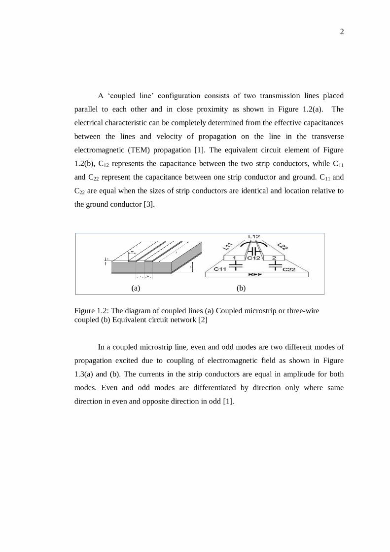
A ‘coupled line’ configuration consists of two transmission lines placed
parallel to each other and in close proximity as shown in Figure 1.2(a). The
electrical characteristic can be completely determined from the effective capacitances
between the lines and velocity of propagation on the line in the transverse
electromagnetic (TEM) propagation [1]. The equivalent circuit element of Figure
1.2(b), C12 represents the capacitance between the two strip conductors, while C11
and C22 represent the capacitance between one strip conductor and ground. C11 and
C22 are equal when the sizes of strip conductors are identical and location relative to
the ground conductor [3].
(a) (b)
Figure 1.2: The diagram of coupled lines (a) Coupled microstrip or three-wire
coupled (b) Equivalent circuit network [2]
In a coupled microstrip line, even and odd modes are two different modes of
propagation excited due to coupling of electromagnetic field as shown in Figure
1.3(a) and (b). The currents in the strip conductors are equal in amplitude for both
modes. Even and odd modes are differentiated by direction only where same
direction in even and opposite direction in odd [1].

3
(a) (b)
Figure 1.3: The modes of propagation (a) Even mode (b) Odd mode [4]
A bandpass filter is a combination of high and low pass filters with specific
frequency range to pass, but not permitted to pass the lower and higher frequencies.
The frequencies are attenuated at the edge of outside the passband region due to two
cut-off frequencies fL and fH.
High Pass RL filter with a roll-off frequency fL and a Low Pass RC filter with
a roll-off frequency fH is cascaded to realize a bandpass frequency response, with that
fL less than fH.
Figure 1.4: Circuit Diagram for a Bandpass Filter [2].

4
Figure 1.5: Frequency response of a Bandpass filter [2].
Ultra wide-band (UWB) is gained by achieving microwave bandwidth with
equal or more than 500 MHz values. Federal Communication Commission (FCC)
has allocated for unlicensed ultra wideband devices with frequency band 3.1-10.6
GHz about 7500 MHz of spectrum frequency. The UWB technology has huge
opportunity in the design of modern application such as vehicular radar, through-wall
imaging, medical imaging, indoor and hand-held systems [5].
Figure 1.6: The diagram of UWB Technology [3]

5
Recently, different methods and structures have been used to develop new
Ultra Wide-band Bandpass filter (UWB-BPF) such as multi-mode resonator (MMR),
pseudo-interdigital stepped impedance resonators (PI-SIRs), combining low pass and
high pass filter etc [6],[7]. However, filter design for UWB applications face many
challenges. One general problem is to avoid electromagnetic interference with many
other existing narrowband communication systems.
Therefore, one method to eliminate the interferences is by having defected
ground structures, DFGs, which disturb the shield current distribution in the ground
plane. The defect in the ground of the microstrip can give rise to increasing effective
capacitance and inductance that results with higher impedance, band rejections and
slow wave characteristics [8].
1.2 Problem Statement
In many applications, the presence of harmonics will degrade the overall
system performance. Hence the harmonics need to be adequately suppressed.
Traditionally, harmonics are filtered using separate filter circuit, hence this
undesirably increase the bulkiness of the whole system circuitry. Thus, a selected
microwave planar filter designed can be further modified in order to improve the
upper stopband performance.

6
1.3 Objectives
The objective of this project is to design a microwave planar bandpass filter
with emphasis on upper stopband performance and to employ modification into the
bandpass filter structure for better stopband.
1.4 Scope of Project
The project is a continuation of a previous work [8]. It is further improved
with different DFG structures. The designed filters are then simulated and
investigated in terms of its return loss and insertion loss responses. The configuration
of the ground layer is modified by integrating defected structure to improve the upper
stopband region. Circuit simulations are carried out using CST Microwave Studio®.
The performances of all the results are analysed to monitor the harmonic suppression
in the upper region.

7
1.5 Thesis Layout
The content of the thesis is organized into five (5) chapters. The introduction
and overview of the project are described in the first chapter. The second chapter
presents relevant brief theory and literature reviews related to the behaviour of UWB
Bandpass filter and DFG structure. The design methodology is presented in chapter
three. Simulation results obtained are analysed and discussed. The final chapter
concludes the thesis and identify some areas for recommendation and future work.

119
REFERENCES
1. David M. Pozar, “Microwave Engineering Third Edition”, John Wiley and
Sons, 2005.
2. “Microwave Filter”, https://en.wikipedia.org/Microwave_filter
3. Jim Silverstrim “IEEE Ultra wideband Presentation”, IWT - Leading edge
wireless solutions, October 21, 2003.
4. “Transmission Line Basic Theory”, Presentation paper,
http://dowload.intel.com/education.
5. “Revision of Part 15 of the Commission’s rules regarding ultra-wideband
transmission system,” Federal Communication Council, Washington, DC,
Tech. Rep. ET- Docket 98-153, April 2002.
6. Lei-Zhu, Senior Member, IEEE, Sheng-Sun, Student Member, IEEE and
Wolfgang Menzel, Fellow, IEEE, “ Ultra-Wideband (UWB) Bandpass Filters
Using Multiple-Mode Resonantor”, IEEE Microwave and Wireless
Components Letters, Vol.15,, No.11, November 2005.
7. Ming-Zhong Ji, Qing-Xin Chu, and Fu-Chang Chen, “ A Compact UWB
Bandpass Filter Using Pseudo-Interdigital Stepped Impedance Resonantors”,
ICMMT2008 Proceedings, 2008.
120
8. L. H. Weng, Y. C. Guo, X. W. Shi, and X. Q. Chen, “An Overview On
Defected Ground Structure” Progress In Electromagnetics Research B, Vol. 7,
173–189, 2008.
9. Inder Bahl and Prakash Bhartia, “Microwave Solid State Circuit Design”, 2nd
Edition, Wiley: New Jersey, 2003.
10. Qing-Xin Chu, Xu-Kun Tian, “Design of a Compact UWB Bandpass Filter
with Notched Band”, Proceedings of Asia-Pacific Mircowave Conference
2010.
11. Shu-Toa Li, Qing-Xin Chu, “A Compact UWB Bandpass Filter With
Improved Upper-Band Performance”, ICMMT2008 Proceedings, 2008.
12. X.-K. Tian and Q.-X. Chu, “A Compact UWB Bandpass Filter With Improved
Out-of-Band Performance Using Modified Coupling Structure”, Progress In
Electromagnetics Research Letters, Vol. 22, 191-197, 2011.
13. Jae-Kwan Lee and Young-Sik Kim, Member, IEEE, “Ultra-Wideband
Bandpass Filter With Improved Upper Stopband Performance Using Defectec
Ground Structure”, IEEE Microwave and Wireless Components Letters,
Vol.20, No.6, June 2010.
14. Cong-Liu and Jun-Xu, “Ultra-Wideband Bandpass Filter With Dual Notched
Bands Using Hybrid Microstrip/CPW Structure”, IEEE Microwave and
Wireless Components Letters 2011
15. Qing-Xin Chu, Member, IEEE, and Xu-Kun Tian, “Design of UWB Bandpass
Filter Using Stepped-Impedance Stub-Loaded Resonator”, IEEE Microwave
and Wireless Components Letter, Vol.20, No.9, September 2010.

121
16. Sina Akhtarzad, Thomas R. Rowbotham, and Peter B. Johns, “ The Design of
Coupled Microstrip Lines”, IEEE Transactions on Microwave Theory and
Techniques, Vol.MTT-23, No.6, June 1975
17. Norhaslinda Hassan, “Compact Microwave Microstrip Fractal Filter with
suppressed second harmonic”, Dissertation of Degree of Electrical-
Telecommunicaton Engineering FKE UTM, May 2009.
18. Park, J.I., C.-S Kim, et al., “Modeling of photonic bandgap and its
application for the low-pass filter design.” Asia Pacific Microwave Conf.
APMC, Vol.2, 331-334, 1999.
19. Devendra K. Misra, “Radio-Frequency and Microwave Communication
Circuits Analysis and Design 2nd
Edition”, John Wiley and Sons, 2004.
20. Ching- Luh Hsu, Fu- Chieh and Jen-Tsai Kuo, “ Microstrip Bandpass Filters
For Ultra-Wideband (UWB) Wireless Communication”, IEEETransactions on
Microwave Theory and Techniques, 2005.
21. Sudipta Das, Dr. S.K.Chowdhury, “Design Simulation and Fabrication of
Stepped Impedance Microstripline Low Pass Filter for S-band Application
using IE3D and MATLAB”, IJECT Vol. 3, Issue 1, Jan. - March 2012
22. Lei Zhu, Wolfgang Menze, Ke Wu, Frank Boegelsack, “ Theoretical
Characterization and Experimental Verification of a Novel Compact
Broadband Microstrip Bandpass Filter”, Proceedings of APMC2001, 2001
23. Lei Zhu, Huuheng Bu, and Ke WuAPERTURE, “ Compesation technique for
innovative design of ultra-broadband microstrip bandpass filter”,Department
of Electrical & Computer Engineering Ecole Polytechnique, University of
Montreal, Quebec, Canada