Embed Size (px)
Citation preview

Modulator Design Modulator Design for Plasma Ion for Plasma Ion ImplantationImplantation
Professor Michael Bradley Professor Michael Bradley Dale Heggie, Joel Leslie, Curtis Dale Heggie, Joel Leslie, Curtis
OlsonOlsonMarch 24March 24thth, 2004, 2004

ObjectiveObjectiveConvert an existing vacuum Convert an existing vacuum
chamber into a plasma ion source chamber into a plasma ion source for Ion Implantationfor Ion Implantation

Applications in Materials Applications in Materials ProcessingProcessing
1.1. Electronics IndustryElectronics Industry• Semiconductor dopingSemiconductor doping• IC FabricationIC Fabrication
2.2. Mechanical Mechanical TreatmentTreatment
• Surface hardnessSurface hardness• Frictional PropertiesFrictional Properties
3.3. Biomedical ImplantsBiomedical Implants• Biocompatible materialsBiocompatible materials

What’s a plasma??What’s a plasma??
Four States of Four States of MatterMatter
1.1. SolidSolid
2.2. LiquidLiquid
3.3. GasGas
4.4. PlasmaPlasma

Plasma ExamplesPlasma Examples
Neon Neon lightslights
LightninLightningg
SunSun Aurora Aurora
BorealisBorealis

Plasma ExamplesPlasma Examples
Neon Neon lightslights
LightninLightningg
Aurora Aurora BorealisBorealis

PII Material ProcessingPII Material Processing
1.1. Insert sample Insert sample into chamberinto chamber
2.2. Strike a Strike a plasmaplasma
3.3. Apply high Apply high negative negative voltagevoltage
4.4. Ions hit the Ions hit the sample and sample and are implantedare implanted
+ + + + + + +Silicon
-5 kV

PII Material ProcessingPII Material Processing
-5 kV
+ + + +
Characterize the Characterize the effects of implant effects of implant depth and dosedepth and dose
-10 kV-20 kV
Sample MaterialSample Material
Sample HolderSample Holder

Implant ImplicationsImplant Implications
Kinetic energy is Kinetic energy is transferred into transferred into heatheat
Sample Sample overheating from overheating from continuous implantcontinuous implant
Requires pulsed Requires pulsed voltagevoltage
+ + + + + + +

Voltage PulsingVoltage Pulsing
Energy Energy contaminaticontamination from on from rising and rising and falling falling edgesedges
Time
Voltage
Implanting Cooling
+ + + + + + + + +

Final SystemFinal System
+ -
High Voltage Source
Modulator
Vacuum Chamber

Modulator DesignModulator Design
Solid state Solid state transistor transistor modulesmodules
One master One master timer timer
ExpandableExpandable
Time Start
Master Timer
Optical Fiber
+ -
High Voltage Source
To Vacuum

Final System Final System

Circuit PerformanceCircuit Performance
5 switching 5 switching modulesmodules
Excellent Excellent rise and fall rise and fall timestimes
Expandable Expandable without without affecting affecting performanceperformance
TimerTimerHigh VoltageHigh Voltage

Successful ImplantSuccessful Implant
5 switching modules 5 switching modules 1600 V negative 1600 V negative
biasbias 2” Silicon Wafer2” Silicon Wafer Short Nitrogen Short Nitrogen
implantimplant

Special ThanksSpecial Thanks
Dr. Michael BradleyDr. Michael Bradley Dave McColl, P. Eng.Dave McColl, P. Eng. Dr. Ajay SinghDr. Ajay Singh Dr. Akira HiroseDr. Akira Hirose Perry BalonPerry Balon Vic Meyer, Electrical Vic Meyer, Electrical
ShopsShops

Questions???Questions???

Master ControllerMaster Controller
Circuit DescriptionCircuit Description Monostable 555 for Monostable 555 for
implant durationimplant duration Astable 555 for Astable 555 for
pulse frequencypulse frequency FeaturesFeatures
Duty cycle variationDuty cycle variation Implant Time (5, Implant Time (5,
10, 30 seconds)10, 30 seconds) Start ControlStart Control

Circuit DevelopmentCircuit Development
High Voltage Switching UnitsHigh Voltage Switching Units PC Board layout in TraxmakerPC Board layout in Traxmaker Fabricated by Electrical Engineering ShopsFabricated by Electrical Engineering Shops

Vacuum Chamber Vacuum Chamber ResultsResults
• 2 x 102 x 10-7-7 Torr base pressure Torr base pressure• 0.01% impurities from background 0.01% impurities from background
gasgas
Vacuum Chamber Pump Down Curve
1.00E-07
1.00E-06
1.00E-05
1.00E-04
0 0.5 1 1.5 2 2.5
Time (days)
Pre
ssu
re (
To
rr)

Sample HolderSample Holder
Secure silicon Secure silicon wafer inside wafer inside chamberchamber
Thermal Thermal conductivityconductivity AluminumAluminum
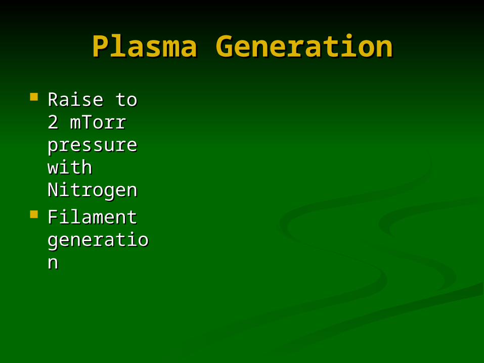
Plasma GenerationPlasma Generation
Raise to 2 Raise to 2 mTorr mTorr pressure pressure with with NitrogenNitrogen
Filament Filament generatiogenerationn

Testing Testing

By the Numbers…By the Numbers…
Vacuum ChamberVacuum Chamber• Goal - Base pressure < 1 µTorrGoal - Base pressure < 1 µTorr Result – 2 x 10Result – 2 x 10⁻⁷-7 Torr Torr
High Voltage SwitchingHigh Voltage Switching• Goal - < 10 microsecond rise and Goal - < 10 microsecond rise and
fallfall Result – 300 ns rise, 700 ns fallResult – 300 ns rise, 700 ns fall

Switching ProblemsSwitching Problems
• Less than 1% energy contaminationLess than 1% energy contamination

Overall Circuit Overall Circuit PerformancePerformance
• 5 modules at 1600 5 modules at 1600 VoltsVolts
• Expandable without Expandable without affecting performanceaffecting performance

Vacuum ChamberVacuum Chamber
Base pressureBase pressure 1 in 10 000 1 in 10 000
contaminationcontamination

Langmuir ProbeLangmuir Probe
Characterize our Characterize our plasma for accurate plasma for accurate implant dosesimplant doses
Ion saturation Ion saturation current of 12 mAcurrent of 12 mALangmuir Probe Curve
-14-12-10-8-6-4-2024
-40 -30 -20 -10 0
Voltage (V)
Cur
rent
(mA
)
Isat
Vf loat(-5v)
Langmuir Probe Curve
-100
0
100
200
300
400
-40 -30 -20 -10 0 10
Voltage (V)
Cu
rren
t (m
A)
Isat
Vf loat(-5v)
Ion Density of Ion Density of Plasma (~2 x 10Plasma (~2 x 1099 ions/cmions/cm33))
0.57% ionization0.57% ionization

Modulator DesignModulator Design
• ModulesModules• Insulated gate Insulated gate
bipolar junction bipolar junction transistor (IGBT)transistor (IGBT)
• Internal battery Internal battery powerpower
• Optical IsolationOptical Isolation• SynchronizationSynchronization

Future Design ProjectsFuture Design Projects
1.1. High Voltage IsolationHigh Voltage Isolation1.1. Metal boxesMetal boxes2.2. Fast Zener clamping for each moduleFast Zener clamping for each module
2.2. Increase Plasma densityIncrease Plasma density1.1. Shorter implant timesShorter implant times2.2. Increase saturation current via RF Increase saturation current via RF
sourcesource3.3. Better Power SupplyBetter Power Supply