Embed Size (px)
Citation preview

Modular Solutions for Next Generation Search and Rescue Helmets
EEL4915L Senior Design II
22 April 2019
Group #21
Anthony, Jacob - Electrical Engineering
Cummings, Shakira - Computer Engineering
Hudson, Stephen - Electrical Engineering
Medrozo, Harriet - Electrical Engineering
Advisors: Dr. Lei Wei, Dr. Samuel Richie

i
Table of Contents 1.0 EXECUTIVE SUMMARY ....................................................................................................1
2.0 PROJECT DESCRIPTION ..................................................................................................2
2.1 MOTIVATION ................................................................................................................................. 2
2.2 GOALS/OBJECTIVES .................................................................................................................... 2 2.2.1 OVERALL SYSTEMS OBJECTIVES .................................................................................................................... 2
2.2.1.1 COMMUNICATIONS MODULE.................................................................................................................. 2 2.2.1.2 AUGMENTED VISION MODULE .............................................................................................................. 4 2.2.1.3 LOCALIZED LOCATION MODULE........................................................................................................... 4 2.2.1.4 POWER MODULE .......................................................................................................................................... 5
2.3 OVERALL SPECIFICATIONS AND CONSTRAINTS ............................................................... 5 2.3.1 Overall Specifications ........................................................................................................................................... 5 2.3.2 Constraints ................................................................................................................................................................ 6
2.5 Overall High Level Block Diagram......................................................................................... 6
2.6 House of Quality ........................................................................................................................... 7
3.0 RESEARCH ..........................................................................................................................8
3.1 EXISTING PRODUCTS.................................................................................................................. 8 3.1.1 ROCKWELL COLLINS ............................................................................................................................................ 8 3.1.2 JOHAN SPORTS ........................................................................................................................................................ 9
3.1.2.1 GPS ....................................................................................................................................................................... 9 3.1.2.2 IMU .................................................................................................................................................................... 10 3.1.2.3 Sensor Fusion ............................................................................................................................................... 10 3.1.2.4 Filter Techniques ........................................................................................................................................ 10 3.1.2.5 Problems with the Johan Sports Tracking Device ........................................................................ 11 3.1.2.6 Coordinate Systems ................................................................................................................................... 11 3.12.7 Earth Coordinate Frame ........................................................................................................................... 11 3.1.2.8 World Coordinate Frame ......................................................................................................................... 12 3.1.2.9 Earth Frame to World Frame ................................................................................................................. 12 3.1.2.10 World Frame to Field Frame ............................................................................................................... 13 3.1.2.11 Parts ............................................................................................................................................................... 13 3.1.1.12 Body coordinate plane .......................................................................................................................... 13 3.1.2.13 Sensor Coordinate Frame ..................................................................................................................... 14 3.1.2.14 Calibration of the Accelerometer and the Gyroscope .............................................................. 14
3.1.3 MODULAR HELMET DESIGNS ......................................................................................................................... 15 3.1.3.1 SOLAR POWERED SKI HELMET ........................................................................................................... 16
3.2 MARKET ANALYSIS .................................................................................................................. 16 3.2.1 TARGET DEMOGRAPHIC ................................................................................................................................... 17
3.2.1.1 SAFETY AND RESCUE TEAMS ......................................................................................................... 17 3.1.1.2 MILITARY ................................................................................................................................................. 17 3.2.1.3 RECREATIONAL USE ........................................................................................................................... 17
3.2.2 Target market ......................................................................................................................................................... 17 3.2.3 MARKET NEED ...................................................................................................................................................... 19 3.2.4 COMPETITION ....................................................................................................................................................... 20 3.2.5 BARRIERS TO ENTRY ......................................................................................................................................... 20 3.2.6 REGULATIONS ....................................................................................................................................................... 21
3.3 RELEVANT TECHNOLOGIES ................................................................................................... 22

ii
3.3.1 TWO-WAY RADIO ................................................................................................................................................. 22 3.3.2 SOLAR PANELS ...................................................................................................................................................... 23
3.3.2.1 Photovoltaic Panels (PV) ......................................................................................................................... 23 3.3.2.1 Monocrystalline ..................................................................................................................................... 24 3.3.2.2 Polycrystalline ........................................................................................................................................ 24
3.3.2.2 Battery Charge Controller ....................................................................................................................... 24 3.3.2.3 Trickle charging ........................................................................................................................................... 25 3.3.2.4 Battery ............................................................................................................................................................. 25
3.3.2.4.1 Lithium ion ........................................................................................................................................... 25 3.3.2.4.2 Nickel-Metal Hydride ....................................................................................................................... 25
3.3.3 CAMERAS ................................................................................................................................................................. 26 3.3.4 CELL PHONES ......................................................................................................................................................... 27 3.3.5 REGULATORS ......................................................................................................................................................... 27
3.3.5.1 Standard Linear regulators..................................................................................................................... 27 3.3.5.2 LDO (Low Drop Out) Regulators .......................................................................................................... 28 3.3.5.3 Switching regulators .................................................................................................................................. 28 3.3.5.4 Buck converter ............................................................................................................................................. 28 3.3.5.5 Boost converter ........................................................................................................................................... 29 3.3.5.6 Buck Boost Converter ............................................................................................................................... 30
3.3.6 Heat Sink ................................................................................................................................................................... 31 3.3.7 Battery chargers .................................................................................................................................................... 31
3.4 PART SELECTION ...................................................................................................................... 31 3.4.1 COMMUNICATIONS MODULE ......................................................................................................................... 31
3.4.1.1 Transceiver .................................................................................................................................................... 33 3.4.1.2 RF Amplifier .................................................................................................................................................. 34 3.4.1.3 Antenna ........................................................................................................................................................... 35 3.4.1.4 Microphone/Headphone ......................................................................................................................... 36 3.4.1.5 SOFTWARE FOR COMMUNICATIONS MODULE ............................................................................ 36
3.4.2 AUGMENTED VISION MODULE ...................................................................................................................... 38 3.4.2.1 Display Screen ........................................................................................................................................ 39 3.4.2.2 IR beacon .................................................................................................................................................. 39 3.4.2.3 File Storage .............................................................................................................................................. 39 3.4.2.4 Control Unit ............................................................................................................................................. 39
3.4.3 LOCALIZED LOCATION MODULE .................................................................................................................. 40 3.4.3.1 Arduino UNO ................................................................................................................................................. 41
3.4.3.1.1 ARDUINO UNO .............................................................................................................................. 41 3.4.3.1.2 ARDUINO NANO ........................................................................................................................... 41 3.4.3.1.3 ARDUINO PRO MINI ................................................................................................................... 42
3.4.3.2 ATTINY85 ....................................................................................................................................................... 42 3.4.3.3 ATMEGA328 CHIP ...................................................................................................................................... 42 3.4.3.4 ATTINY85 CHIP ........................................................................................................................................... 43 3.4.3.5 Accelerometer .............................................................................................................................................. 43 3.4.3.6 Gyroscope ....................................................................................................................................................... 44 3.4.3.7 Magnetometer .............................................................................................................................................. 44 3.4.3.8 Global Positioning System Technology (GPS) ................................................................................ 44 3.4.3.9 MEMS ................................................................................................................................................................ 45 3.4.3.10 FOG VS MEMS ............................................................................................................................................. 45 3.4.3.11 Strategic Components and Parts for Localized Locations Module ..................................... 49
3.4.3.11.1 Copernicus II GPS Receiver .................................................................................................. 49 3.4.3.11.12 ICM -20948: low power 9-axis MEMS Motion Tracking Device ........................ 50
3.4.3.12 SOFTWARE .................................................................................................................................................. 50 3.4.3.12.1 UART .................................................................................................................................................... 51 3.4.3.12.2 I2C .......................................................................................................................................................... 51 3.4.3.12.3 SPI .......................................................................................................................................................... 51

iii
3.4.4 POWER MODULE .................................................................................................................................................. 52 3.4.4.1 Photovoltaic Cells ........................................................................................................................................ 53 3.4.4.2 Sequencers ..................................................................................................................................................... 53
3.4.4.1.2 .1 LM3380 ............................................................................................................................................. 53 3.4.4.1.2.2 LM3881 .............................................................................................................................................. 54 3.4.4.1.2.3 LT1371 ............................................................................................................................................... 54 3.4.4.1.2.24 LT1371............................................................................................................................................. 54
3.4.4.3 Step Down Voltage Regulators .............................................................................................................. 55 3.4.4.3.1 LM2597 .................................................................................................................................................. 55 3.4.4.3.2 TPS82150 .............................................................................................................................................. 55 3.4.4.3.3 Low Drop-Out Voltage ..................................................................................................................... 55
3.4.4.3.3.1 TLV702 ......................................................................................................................................... 55 3.4.4.3.3.2 TLV700 ......................................................................................................................................... 56 3.4.4.3.3.13 LT1512 ....................................................................................................................................... 56 3.4.4.3.3.4 Bq2000 ......................................................................................................................................... 57 3.4.4.3.3.5 Bq2954 ......................................................................................................................................... 57
4.0 RELATED STANDARDS AND DESIGN CONSTRAINTS ........................................... 59
4.1 RELATED STANDARDS ............................................................................................................ 59 4.1.1 COMMUNICATIONS MODULE ......................................................................................................................... 59
IEEE 802.15.4 ......................................................................................................................................................... 60 4.1.2 Augmented Vision Module ............................................................................................................................... 61
4.1.2.1 MPEG ................................................................................................................................................................ 61 4.1.2.2 YUV2 / YUYV ................................................................................................................................................. 62
4.1.3 LOCALIZED LOCATION MODULE .................................................................................................................. 62 IEEE 802.22 Geo-location ................................................................................................................................. 62
4.1.4 POWER MODULES ................................................................................................................................................ 62 IEEE Std 1562-2007 GUIDE for array and Battery Sizing in Stand Alone Photovoltaic Systems ..................................................................................................................................................................... 62 4.1.4.1 Solar power standard .......................................................................................................................... 64 4.1.4.2 IEEE Std 1262-1995 IEEE recommended Practice for qualification of photovoltaic PV modules ............................................................................................................................................................. 65 4.1.4.3 EUR 13897 qualification test procedures for crystalline silicon photovoltaic modules .................................................................................................................................................................... 65 4.1.4.4 IEEE STD 1625-2008 IEEE standard for rechargeable batteries for multicell mobile computing devices ............................................................................................................................................... 66 Introduction ........................................................................................................................................................... 66 4.1.4.5 Battery Pack Considerations ............................................................................................................ 66 4.1.4.6 Host Device Considerations .............................................................................................................. 67 4.1.4.7 Adaptors .................................................................................................................................................... 68 4.1.4.8 IEEE Std 1679.1-2017 IEEE guide for the characterization and evaluation of Lithium-Based Batteries in Stationary Applications. ........................................................................... 68 4.1.4.9 Charging/Discharging monitoring and simulation platform for li ion batteries ...... 68
4.1.5 OVERALL STANDARDS ...................................................................................................................................... 69 4.1.5.1 SPI ................................................................................................................................................................ 69 4.1.5.2 UART ........................................................................................................................................................... 69 4.1.5.3 I2C ................................................................................................................................................................ 69 4.1.4.4 USB .............................................................................................................................................................. 69
4.2 DESIGN CONSTRAINTS ............................................................................................................ 69 4.2.3 SIGNAL ATTENUATION ..................................................................................................................................... 70
5.0 SYSTEM DESIGN DETAILS ........................................................................................... 71
5.1 MICROCONTROLLER ................................................................................................................ 71

iv
5.2 HARDWARE DESIGN ................................................................................................................ 71 5.2.1 COMMUNICATIONS MODULE ......................................................................................................................... 71 5.2.1.1 Radio Frequency Communication Basics ............................................................................................... 71 5.2.1.2 General Physics of Radio Signals ................................................................................................................ 71
5.2.1.3 RF Communication Systems Basics .................................................................................................... 72 5.2.1.4 Sub-1Ghz ISM devices ............................................................................................................................... 73 5.2.1.5 Range and Coexistence ............................................................................................................................. 73 5.2.1.6 Modulation and Demodulation ............................................................................................................. 74 5.2.1.7 Modulation Scheme .................................................................................................................................... 76 5.2.1.8 Frequency Shift Key ................................................................................................................................... 77 5.2.1.9 IMPORTANCE OF IMPEDANCE MATCHING .................................................................................... 78 5.2.1.10 RADIO RANGE AND FREE SPACE PROPAGATION .................................................................... 79 5.2.1.11 PRINTED CIRCUIT BOARD LAYOUT DESIGN AND ASSEMBLY ............................................ 79
5.2.2 POWER MODULE ................................................................................................................... 80 5.2.1 DC-DC Conversion ................................................................................................................................................ 80 5.2.3 DC to DC conversion Characteristics............................................................................................................ 84
5.2.3.1 Battery housing ............................................................................................................................................ 85 5.2.3.2 Battery Design Details .............................................................................................................................. 85 5.2.3.3 Solar Panels Design ................................................................................................................................... 86 5.2.3.4 Battery Charger ............................................................................................................................................ 87
5.2.3 AUGMENTED VISION MODULE ...................................................................................................................... 88 5.2.4 LOCALIZED LOCATION MODULE .................................................................................................................. 90 5.4 SOFTWARE OVERVIEW ......................................................................................................................................... 90
5.4.1 AUGMENTED VISION MODULE ................................................................................................................ 90 5.4.2 Computer Vision.............................................................................................................................................. 91 5.4.3 OpenCV ................................................................................................................................................................ 91 5.4.4 Mahotas ............................................................................................................................................................... 92 5.4.5 Skimage ............................................................................................................................................................... 92 5.4.6 Comparison ....................................................................................................................................................... 92 5.4.7 Running on start up ....................................................................................................................................... 94
5.4.7.1 rc.local ........................................................................................................................................................ 94 5.4.7.2 .bashrc ........................................................................................................................................................ 94 5.4.7.3 init.d directory ........................................................................................................................................ 95
5.4.8 Systemd ............................................................................................................................................................... 95 5.4.9 Crontab ................................................................................................................................................................ 95 5.4.10 election ............................................................................................................................................................. 96 5.4.11 Operation on power down ....................................................................................................................... 96 5.4.12 Camera software .......................................................................................................................................... 96 5.4.13 Software for the screen ............................................................................................................................. 97
5.3.13.1 UART ........................................................................................................................................................ 98 5.3.14 I2C ................................................................................................................................................................. 98 5.3.15 SPI ................................................................................................................................................................. 98
5.4.2 Schematics ............................................................................................................................................................... 98 5.4.3 About the PCB Design ...................................................................................................................................... 105 5.4.4 Initial Concept Design Rendering ............................................................................................................... 105
6.0 INTEGRATION AND TESTING ...................................................................................107
6.1 COMPONENT TESTING .......................................................................................................... 107 6.1.1 COMMUNICATIONS MODULE ...................................................................................................................... 107
6.1.1.1 TI 15.4 Stack – Out of the Box Experience .................................................................................... 108 6.1.1.1.2 Basic Receiving and Transmitting Using the Texas Instrument CC1352P ................. 108 6.1.1.1.4 Basic Serial Communications to the Copernicus II ................................................................ 110
6.1.2 AUGMENTED VISION MODULE ................................................................................................................... 111 6.1.3 LOCALIZED LOCATION MODULE ............................................................................................................... 112

v
6.1.3.1 GPS .................................................................................................................................................................. 112 6.1.3.2 Procedure for Testing the GPS Module- Hardware ................................................................... 112 6.1.3.3 ATMEGA328P CHIP ................................................................................................................................. 113
6.1.4 POWER MODULE ............................................................................................................................................... 113
6.2 PCB TESTING ............................................................................................................................ 114
6.3 SOFTWARE TESTING ............................................................................................................. 114 6.3.1 Procedure for Testing the GPS Module- Software ......................................................................... 115 6.3.2 Implementation of OPUS Audio Codec for Voice Compression ............................................... 116 6.3.3 TI real time operating system RTOS Kernel .................................................................................... 118 6.3.4 Sensor and Collector - TI 15.4-Stack Project Zero ........................................................................ 119
7.0 PROJECT OPERATION .................................................................................................123
7.1 SYSTEM BOOT UP ................................................................................................................... 123
7.2 USER OPERATION ................................................................................................................... 123
8.0 ADMINISTRATIVE CONTENT ....................................................................................124
8.1 MILESTONES ............................................................................................................................. 124 8.1.1 INITIAL PROJECT MILESTONE FOR BOTH SEMESTERS ...................................................... 124
8.2 BUDGET ANALYSIS ................................................................................................................. 125 8.2.1 INITIAL PROJECT BUDGET ................................................................................................................ 125
9.0 PROJECT SUMMARY AND CONCLUSION ....................................................................126
10.0 Appendices .....................................................................................................................128
10.1 Works Cited............................................................................................................................ 128
10.2 Permissions ........................................................................................................................... 135

vi
Table of Figures Figure 1 High level System Hardware Block Diagram .......................................... 7 Figure 2 House of Quality Trade Off Table ........................................................... 7 Figure 3 The JOHAN Sports Tracker Device and Charging Station ..................... 9 Figure 4 Earth Coordinate Plane [10] reprinted with permission form Mantis Roobeek ............................................................................................................. 12 Figure 5 World Coordinate Frame [10] With permission from Mantis Roobeek .. 12 Figure 6 Field Coordinate Frame [10] with permission from Mantis Roobeek .... 13 Figure 7 Body Coordinate Frame [10] Reprinted with permission from Mantis Roobeek ............................................................................................................. 14 Figure 8 Solar Powered Ski Helmet with permission form: Giz Mag editor ......... 16 Figure 9 Survival Spending of Americans ........................................................... 18 Figure 10 Google search of Night Vision Helmet ................................................ 19 Figure 11 Basic Set Up of How to Charge. Battery with PV Reprinted with permission from IEEE ......................................................................................... 23 Figure 12 Photovoltaic Cells Reprinted with permission from Green Match ....... 24 Figure 13 LDO Regulator with permission from Analog Devices ........................ 28 Figure 14 Buck Converter with permission from El- Pro-Cus ............................. 29 Figure 15 Boost Converter With permission from El-Pro-Cus ............................ 30 Figure 16 Switching Regulator with permission from Chegg ............................. 30 Figure 17 Parts for Dc-to-DC Converter ............................................................. 85 Figure 18 Accelerometer Schematic ................................................................... 99 Figure 19 Copernicus II GPS schematic ............... Error! Bookmark not defined. Figure 20 Connections for Raspberry Pi, Display Screen, an IR Camera ........ 101 Figure 21 Battery Charging Circuit ................................................................... 101 Figure 22 Power Distribution Circuit ................................................................. 103 Figure 23 CC1352P .............................................. Error! Bookmark not defined. Figure 24 PCB Design ...................................................................................... 104 Figure 25 Concept Design of First Responder Helmet ..................................... 106 Figure 26 Concept Design of First Responder Helmet_1 ................................. 106 Figure 32 PROJECT ZERO RED AND GREEN LED TEST ............................. 108 Figure 33 Receiver Device Control panel receiving packets - reprinted with permission from Texas Instrument ................................................................... 110 Figure 34 Serial tools with Copernicus ii settings ........................................... 111 Figure 37 Test Picture on Ada Fruit ST7735 Display Screen and Test Image Recorded by ELP IR Camera ........................................................................... 112 Figure 38 GPS Module Test, Tremble Copernicus II Wiring, and Arduino UNO Wiring ............................................................................................................... 113 Figure 39 Power module breadboard ............................................................... 113 Figure 40 Serial Monitor Output from GPS reciever ......................................... 116 Figure 39 OPX audio format reprinted with permission from Texas Instrument 117 Figure 40 Successful build of OPUSlib reprinted with permission from Texas Instruments ....................................................................................................... 118 Figure 36 SimpleLink CC13x2 SDK[119] .......................................................... 120 Figure 37 Examples, Development Tools CC1352R LaunchPad .................... 120 Figure 38 CCS collector ................................................................................... 121

vii
Figure 39 config.h ............................................................................................. 121 Figure 40 Collector/Sensor Test ....................................................................... 122

viii
Table of Tables Table 1 Transceiver Module Comparison ........................................................... 34 Table 2 Amplifier Comparison Table .................................................................. 35 Table 3 Microcontroller Comparison_1. .............................................................. 42 Table 4 Microcontroller Comparasion_2 ............................................................. 42 Table 5 Microcontroller Comparasion_3 [120][121] ............................................ 43 Table 6 GPS Comparison [23] ............................................................................ 49 Table 7 IMU Comparison Table .......................................................................... 50 Table 8 Photovoltaic Cells Comparison table ..................................................... 53 Table 9 Switching Regulator Comparison Table ................................................ 54 Table 10 Step Down Voltage Regulator Comparison Table ............................... 55 Table 11 Low Drop Out Comparison Table ........................................................ 56 Table 12 Maximum Permissible Exposure (MPE) Limits – printed with permission from ARRL.org .................................................................................................... 61 Table 13 Frequency Bands Designations [ ......................................................... 72 Table 14 List of Components Receiving Power .................................................. 81 Table 15 Loads on Rails ..................................................................................... 81 Table 16 Battery Information .............................................................................. 83 Table 17 Regulator Specs .................................................................................. 84 Table 18 Comparison of Controllers ................................................................... 88 Table 19 Comparison of Screens ....................................................................... 89 Table 20 Comparison of Cameras ...................................................................... 89 Table 21 Comparison of Computer Vision Libraries ........................................... 93

1
1.0 EXECUTIVE SUMMARY When Group 21 gathered together they began their discussion of what each member hoped to leave this senior design collaboration with. None of the members of group 21 truly had project specific goals that they wanted to attain; so, Group 21 began discussing what they felt were root problems that needed to be solve. One of the ideas spurred the topic of Black Panther. Which brought one of the members to excitedly state that they wanted to create an Iron Man helmet, a fully functional Iron Man helmet to be more exact.
A fully functioning Iron Man helmet was unrealistic as a senior design project. There would be too many complicated systems of that would need to be created: an artificial intelligence (AI), surveillance systems, targeting systems, item recognition software, locations systems, and communications to list a few. Despite how unreachable recreating the Iron Man helmet seemed, Group 21 felt they had a concept to work with.
The question then begged, “Who would benefit from using some of these systems integrated together?” Usually, the military is the first thing that comes to mind when creating an Iron Man-like helmet. However, other groups could use hands free systems, such as: search and rescue crews, doomsday preppers, emergency responders, outdoor hobbyists, and anyone that wants a cool toy.
After Group 21 found its target market, they picked the features that were of necessity to the user: communication, vision, and location. These three systems are the basis of almost all other systems members of the target audience use. Some characteristics of the overall design also needed to be discussed. Many personnel who this project would benefit, as a line of work, have a lot of equipment; so, this system would need to be lightweight. It would need to stay powered as long as possible without external power. This system would also need to be reliable and resistant to bumps and jarring.

2
2.0 PROJECT DESCRIPTION
2.1 MOTIVATION Disaster comes in many forms and it is during those times of stress that Search and Rescue (SAR) Teams deploy. The crews extinguish fires, find the lost, and rescue those in compromised situations. SAR crews must make quick, well- informed decisions at a moment’s notice. Making split-second decisions when lives are on the line is never easy. However, is it possible to augment vision when line of sight is compromised? Would a rescue mission function more flawlessly with a robust and reliable communication system? What possibilities are available if all crewmembers knew each other’s location at any given time? A modular approach to improving the modern search and rescue helmet includes enhanced sight, using night-vision and infrared, with potential for target tracking, personalized location beacons for tracking all SAR crews in action, and a reliable communication system. This proposed modular system merges cutting-edged technology with proven, reliable solutions to provide an enhancement to existing equipment. Its modular design means cost-savings for clients but also has capabilities for full system integration.
2.2 GOALS/OBJECTIVES
The objective of this section is to introduce the overall systems objectives as well as the individual modules and their goals and objectives.
2.2.1 OVERALL SYSTEMS OBJECTIVES
The objective of the systems is as follows: to create a module design that could complete three tasks: see in low light areas, establish a reliable means of communication, and to a means of communicating location. This system aims to enhance situational awareness
2.2.1.1 COMMUNICATIONS MODULE
The objective of the communications module is to provide clear, reliable voice and GPS data communications between users. This is important in search and rescue operations due to the potentially hazardous situations that workers may be in. Clear and reliable communications may be the difference between life and death in hazardous situations.
Potential applications for clear and reliable communications are countless. Some possible uses can be:
Military First Responders Personal/family use in case of emergency Commercial security

3
Sports/coaching communications
To be able to provide clear, reliable voice and GPS data communications, the communications module must be able to do the following:
• Have a reliable system that collects voice and inputs it into the communications module
• A transceiver that is capable of transmitting and receiving data at the appropriate bandwidth
• The bandwidth should be so that it can provide reliable a connection from one device to another, i.e. handle the traffic of data and information that is being transferred between devices
Breaking down the communications module into its individual components, these are the goals of the components of the communications module:
Texas Instruments CC1352R MCU – this component is the microcontroller unit of the communications module. It has two build in processors: one ARM© Cortex© M4F processor, one ARM© Cortex© M0 processor. With that being said, the M4F processor’s goal is to be able to run the application and higher layers of the radio protocol stacks [TI datasheet]. The radio frequency core of the microcontroller unit contains the other processor, the ARM© Cortex© M0 processor. The goal of this processor is to be able to between the analogue RF and base band circuitry. It should be able to process the data that is being transferred between to and from the system CPU, and compile the bits in in a specified packet structure. Since there is a dedicated core-processing unit just for the RF communications, it should be able to reduce power and off-load a lot of the work from the main CPU and enable it to do more processing tasks. This is particularly helpful since the communications module needs to be able to process incoming GPS data from the localized location module.
There are also 2 radios: one capable of transmitting and receiving at sub-1GHZ frequencies and one capable of transmitting and receiving at 2.4GHz. The radio transmitting and receiving at sub-1GHz frequency will be dedicated to voice communications while the radio capable of receiving and transmitting at 2.4GHz will be dedicated to GPS data communications. A good reason to use high frequency carrier waves to send GPS data information is because by using higher frequency waves, the antenna length would then shorten.
The Texas Instruments CC1352R MCU is capable of the following serial communications: SSI, UART, I2S, and I2C.Since the device is capable of a myriad of serial communication interfaces, the following are the goals for each of the serial communications. The UART should be able to handle any asynchronous transmitter and receiver functions between peripherals and the module. The I2S should be able to handle the digital audio and be able to interface with pulse-density modulated microphones.
The device also has an analogue to digital converter (ADC) as well as a digital to analogue converter (DAC). Since the device is capable of a myriad of serial communication interfaces, the following are the goals for each of the serial
4
communications. The UART should be able to handle any asynchronous transmitter and receiver functions between peripherals and the module. The I2S should be able to handle the digital audio and be able to interface with pulse-density modulated microphones.
2.2.1.2 AUGMENTED VISION MODULE
The augmented vision module needs to enable the user to see in low light conditions. The module needs to be able to see in smoky conditions, at night, or in places where there is little to no natural light, such as caves or buildings. The module will need four separate pieces of hardware: a camera sensor, an IR illuminator, an IR beacon, a display screen, a file storage device, and a control unit. The augmented vision module will provide visual tracking to ‘friendly’ helmets that will have their IR beacon integrated. The module will also be able to identify open flame or other objects that produce high amounts of IR radiation. When the module detects on of the two listed items it will place a visual indicator on screen. When detecting objects with high IR radiation the module will beep to alert the user. Some information will be available to display such as compass heading and location.
The immediate goals of the augmented vision module are to be able to stream a video from the NIR camera to a mounted screen, To be able to clearly view and work with images at five meters, to be able to record the streamed video on a data storage device, to be able to have visible IR beacons for others with the same hardware to locate within ten meters. The extended goals of this module are to extend the viewing range up to ten meters and to be able to identify an IR beacon at twenty meters. The reach goals for the augmented vision module is to be able to identify and track targets, view images with a minimum range of fifteen meters and to identify IR beacons at 30 meters.
2.2.1.3 LOCALIZED LOCATION MODULE
If someone from our rescue team is in trouble, finding their location will be of utmost importance. The rescue safety helmet design will have a location module for reasons such as this. For this device, an accelerometer, along with a magnetometer, a gyroscope, and a global positioning system technology (GPS) will be the best option for the location module. This method of locating will not run into the problems that a WIFI locator would have in, say for instance, finding a connection in a building with a falling infrastructure.
Cell phones already use this technology. They use motion tracking to know the position the phone is oriented in and where the phone is in physical space [6]. This information is sent by pings to multiple satellites calculating where you are based on angles of intersection (GPS).
The rescue and safety helmet would use a 9-axis motion tracking device and a GPS. The 9-axis motion tracking device is designed for battery-operated high-performance consumer products. It is made up of a 3-axis accelerometer, a 3- axis gyroscope, and a 3-axis magnetometer. The 9-axis motion tracking device is light

5
in weight, making it a good choice to add to a design that needs to weigh as little as possible. The MEMS (micro-electro-mechanical systems) gyroscopes, for example, are small enough to fit inside a phone.
The immediate goal is to track the location of the safety and rescue helmet. The extended goal is to make the tracking more accurate. More specifically, to make the gyroscope < 10 degrees away from the GPS heading.
2.2.1.4 POWER MODULE
The power module needs to provide power to all the peripherals for a sustained amount of time. It will do this by sending the appropriate amount of voltage to each component thru a system of rails. Each rail will have will provide a hardwired voltage to each component on it.
The battery will provide the rails with the power it needs to power the rails, in order to do this for a sustained amount of time it will be a reachable battery. There will be no primary batteries in this design. The battery will be light weight and small enough to be able to be carried on the user of the first responder helmet.
The battery will be charged by the battery charger, the battery charger will be specifically designed to handle the battery that will be sued in conjunction with it. Meaning that the output current and output voltage will be specifically designed for the battery being used.
There will also be solar cells that will trickle charge the first responder helmet. These solar cells will provide the battery directly with extra charge. These monolithic cells will be places on the roof of the helmet to ensure maximum charge when exposed to direct sunlight.
2.3 OVERALL SPECIFICATIONS AND CONSTRAINTS
This section aims to first give an overall list of specifications for the final product. It then continues to outline the constraints of the final product in more detail.
2.3.1 OVERALL SPECIFICATIONS
Device to provide direction, orientation, and location GPS will provide accuracy a minimum of 3 meters Transceiver will be able to transmit and receive signals in the sub-1GHz
range Communications module to transmit voice at minimum 2 meters
Communications module to provide clear, reliable voice and GPS data communications from helmet-to-helmet and helmet-to-base station
Night-vision capabilities (IR band) at 10 meters Images will be able to be saved for reviewing at a later time IR beacon to display at 25 meters Night vision at 20 meters Range detection with potential for tracking technology

6
Power supplied will be 14400mAh for 24 hours or 7200mAh for 12 hours
2.3.2 CONSTRAINTS
This section will outline the various constraints associated with the project. There are five major constraints that will affect the final product either in design or function:
Budget Time Range/Antenna Reach Federal/State Regulations Experience and knowledge in the field of engineering
Budgetary constraints will be so that the maximum for both helmets should cost around $1500. This constraint is mainly due to student self-funding. The students of the group have decided to split the cost of the total project four ways since there are a total of four students. The total amount that each team member will contribute monetarily will be $375 each. The members of the group agreed to transfer funds using CashApp or Venmo. Budgetary constraints are such an important constraint due to the design’s potential to be extremely high tech. There is always a tradeoff between the component’s capabilities and the cost of the components. Components and parts that typically perform at a higher level are also more expensive. Therefore, caution was taken to balance the budgetary constraints without having a large impact on performance.
Time is an important factor because it put a strain on the timelines for research, concept design, components selection, component ordering, component testing, redesign and production. The turn around time for the engineering cycle to take place, from concept to fully developed and functioning product must be done within two semesters.
Another constraint will be the Antenna range, as it will be limited to multiple factors. One of the main factors is that power output for a non-licensed band is limited to 10mW. Due to the power output being so low, the range of the device will be severely limited. Also, along the same lines, there are multiple federal and state regulations that accompany transmission of radio frequency signals.
All the members participating in this project are undergraduate and therefore have limited design experience and knowledge on these specialized systems. All members have researched and interviewed specialists in the field of their specialized module to gain information.
2.5 Overall High-Level Block Diagram

7
Figure 1 High level System Hardware Block Diagram
2.6 House of Quality
Figure 3 is the house of quality table
Figure 2 House of Quality Trade Off Table
8
3.0 RESEARCH This section will cover topics such as existing products currently on the market, market analysis, market need, relevant technologies, and parts selection for each module.
3.1 EXISTING PRODUCTS
The market for situational awareness products covers government, military, and consumer products alike. The following section outlines several products currently on the market that may utilize similar technologies as the final product of this project.
3.1.1 ROCKWELL COLLINS
Rockwell Collins premiered their CHUCK module equipped with Enhanced Reality Vision System (ERV-30) and FasTAK Integrated Targeting System and Communications Gateway at the 2018 Association of the United States Army Annual Meeting and Exposition in October 2018. The Enhanced Reality Vision System (ERV-30) aims to give warfighters an advantage in situation awareness utilizing augmented reality and delivering via waveguide display, similar to the Head’s Up Display found on fighter jets and motorcycle helmets [25]. The device is small, about the size of an eyeglass lens, lightweight, and can mount on the soldier’s helmet or goggles and delivers digital information for the soldier to view [25]. The display features a 30° diagonal field of view with infinite focal distance [25]. It has full RGB display with the image resolution of 640x360 portrait [25]. The device connects via HDMI and USB, and provides hands-free option, connecting via rail mount accessory to the warfighter’s helmet [25]. Lastly, it provides enhanced vision in both daylight and nighttime conditions with automatic dimming to adjust for light conditions [25]. Rockwell’s FasTAK Integration Targeting System and Communications Gateway is a cross-platform (Windows and Android), secure targeting and communications module that sends and receives digital text messages, provides GPS location, with power and data management integrated into one module [26]. Its targeting system is highly customizable and configurable allowing for a laser range finder, tactical PC, video downlink receiver, digital targeting software amongst other supporting systems [26]. At first glance, it seems that Rockwell’s CHUCK module is very similar to that of this project. However, this project seeks to differentiate itself from the Rockwell module by several factors: cost-effective, modular in design with full integration capabilities, and scalable for both large and small budgets. The design intent with this project is that search and rescue operations can be held by organizations with both large and small budgets. Although bigger budgets can often afford more enhanced technologies, the base should always be the same: reliable solutions. A modular approach to improving the modern search and rescue helmet includes enhanced sight, using night-vision and infrared, personalized location beacons for tracking all search and rescue crews in action, and a reliable communication system. This proposed modular system merges cutting-edge technology with proven, reliable solutions to provide

9
an enhancement to existing equipment. Its modular design means cost-savings for clients but also has capabilities for full system integration.
Using a helmet mounted camera is not new, using low light mounted cameras are not new. Rockwell Collins released their Integrated Digital Vision System (IDVS) in 2016 [71]. This system uses digital cameras mounted on a helmet to aid the user in low light situations cleaning up the image and provides digital data overlays on the screen [71]. The system allows the user to have a 40-degree field of vision with minimal interference with regular sight. The problem with this design is that the cameras used are not cheap and not easy for regular consumers to purchase or use. The problem with this product is that it is too costly and complex for a civilian to be able to acquire and use.
3.1.2 JOHAN SPORTS
Motion tracking systems to measure a sports player’s position, velocity and acceleration are starting to become more present in today’s technologies. Companies such as Johan Sports have developed a device that contains a 9-DoF (Degrees of Freedom) MEMS Inertial Measurement Unit(IMU) and a GPS receiver. In addition, a four-sensor fusion algorithm is used to further filter disturbances [10]. The tracking device is worn in a vest on the player’s upper back and obtains the data [10]. In the same way, the safety and rescue helmet will use a motion tracking sensor and GPS to locate the team members of the rescue team during their missions.
Figure 3 The JOHAN Sports Tracker Device and Charging Station
3.1.2.1 GPS
The device itself is oval shaped and hockey puck sized. Several of the devices are stored in a suitcase that is used as a charging station and to upload the quantified data to the Johan Sports Servers. First looking at the GPS, the GPS of the device uses the satellites that are part of the Global Navigation Satellite System(GNSS) to quantify the devices whereabouts from Earth. The integrated circuit determines the speed estimate from the quantified location when no direction is included. The main problem with the filter operation in the GPS is that is leads to location approximations to not be zero-mean white noise(ZMWN) [10].
10
3.1.2.2 IMU
The IMU of the Johan Sports Tracking Device has an accelerometer, gyroscope, and magnetometer. The accelerometer measures the gravitational acceleration and acceleration of the athlete. The tracking device has to use 3D orientation, because the total quantified acceleration caused by gravity, is hard to distinguish from the acceleration cause by the translational motion. Ideally, the gyroscope should perform dead reckoning, take the current direction the athlete is facing and pin down each next direction/position of the athlete by incorporating the angular velocity over time. However, real gyroscopes do not work as well, because of errors caused by biases, consistently overestimating or consistently underestimating, and noise. Likewise, the best magnetometer would quantify only the Earth’s magnetic field, where the vector would point toward the magnetic North, where the north end of a compass needle points in the direction of Earth’s magnetic field. Instead, there are more magnetic fields that exist, other than Earth’s magnetic field, making the quantification of the sensor deviate for a short time [10].
3.1.2.3 SENSOR FUSION
The sensor fusion of the Johan Sports Tracking Device is used to approximate the orientation, position and velocity of the athlete. The most important information to know is the acceleration and deceleration of the athlete, in order to know the load on the athlete’s muscles. The four-sensor fusion is a Kalman filter, that approximates the rotational motion of the athlete. The common types of filters that can be used in the Johan Sports Tracking Device to approximate rotational motion are the Traditional Linear Kalman Filter and the Unscented Kalman Filter(UKF). The problem with the sensor fusion is that the filters in their present phase cannot precisely approximate the athlete’s accelerations from the sensors in the Johan Sports Tracking device [10].
3.1.2.4 FILTER TECHNIQUES
Filter techniques have to be used for the Johan Sports Tracking Device, because, when in use, it has rotational motion that causes the system to not be in a straight line, nonlinear. To quantify a nonlinear system several filter systems can be used. The Extended Kalman Filter(EKF) takes a nonlinear system and linearizes it, before using the linear Kalman Filter equations. The UKF choses points from the nonlinear models and linearizes them. The linearized points are then used to approximate the new phase. The UKF outshines the EKF when approximately for very nonlinear systems. The UKF performs all processes at once. The Madgwick Filter is another filter that splits the phase approximation into a rotational and translational part, instead of approximating everything at once like the UKF. The leverage of this approach is that the accelerometer can be used as two different things. The accelerometer can be used as a ‘gravity sensor’ to approximate orientation. It can also be used as an ‘acceleration sensor’ in approximating the part of the state vector that moved (translational). The Madgwick Filter uses a first-
11
order iterative optimization algorithm to find the position that best matches the gyroscope, accelerometer, and magnetometer measurements .The rotational state can be quantified by the UKF or Madgwick Filter. Translational motion in linear situations can be found by using the Linear Kalman Filter. The Translational model, when including the directionless speed approximation from the GPS receiver, becomes nonlinear allowing the UKF to be used [10].
To get the best sensor fusion algorithm for the Johan Sports Tracking Device different filters were compared. To approximate the full state the UKF was the best choice. To approximate the rotational motion the Kraft filter, a quaternion-based unscented Kalman filter, and a Madgwick filter were compared. Lastly, the UKF and linear Kalman filter were compared for approximating translational motion [10].
3.1.2.5 PROBLEMS WITH THE JOHAN SPORTS TRACKING DEVICE
The Johan Sports Tracking Device GPS module has offsets in the short term. The filtering action done on the chip causes the noise on the position approximation to not be ZMWN. This is difficult to filter out. Approximating velocity can be done by taking the derivative of the position approximations or by taking the integral of the accelerations. There are problems that arise from taking the derivative of the position and integrating the acceleration. When the derivative is taken of the position, there are peaks in the approximated velocity caused by the sudden jumps from quantified noise, called noise amplification. Integrating the acceleration causes a snowball effect of blunders. It is also difficult to approximate the orientation of the tracking device. Movement muddles the gravity quantifications or causes dead reckoning in the gyroscope causing multiple blunders [10]. Another problem is the small signal noise ratio of athlete’s acceleration and gravity acceleration; where an athlete’s acceleration ranges from -3 to 3 m/s^2, while the acceleration of gravity is 10 m/s^2. The small signal noise ratio makes it difficult to get the wanted measured signal to approximate acceleration [10].
3.1.2.6 COORDINATE SYSTEMS
The GPS sensor quantifies position with relation to the center of the Earth; while the IMU sensor quantifies accelerations, rotations, and direction of the magnetic north with relation to the tracking device. Because of this, the sensor measurements have to be transformed to the field coordinate frame using coordinate transformation [10].
3.12.7 EARTH COORDINATE FRAME

12
The Earth Coordinate System is an Earth-Centered-Fixed (ECEF) coordinate system. ECEF is when the center of the coordinate system lies at the center of the Earth. Moreover, it rotates with the Earth. The Earth frame gives the whereabouts of a point on Earth in degrees of latitude and longitude; where latitude is the vertical angle between the given location and the equatorial plane and longitude is the horizontal angle between the given location and “the reference meridian crossing through Greenwich(UK). “ For latitude, north is the positive direction. For longitude, east is the positive direction [10].
Figure 4 Earth Coordinate Plane [10] reprinted with permission form Mantis Roobeek
3.1.2.8 WORLD COORDINATE FRAME
The World Coordinate System is fixed on Earth’s surface. “The origin is at the location of the first GPS measurement in the dataset. The x-axis points at the ‘magnetic north’, the y-axis points at the ‘magnetic west’. The y-axis is parallel to Earth’s surface and” at a right angle to x. “ the z-axis pointe upwards [10].”
Figure 5 World Coordinate Frame [10] With permission from Mantis Roobeek
3.1.2.9 EARTH FRAME TO WORLD FRAME

13
To transform the Earth frame to the World frame the Haversine formula is used. The Haversine formula calculated the great circle distance and bearing between two points on a sphere[10].
3.1.2.10 WORLD FRAME TO FIELD FRAME
To transform the World frame to the Field frame is simple in concept. The World frame is rotated and translated to become the Field frame. The information collected is turned on the other side of the angle that is between the x-axis of the Field frame and the 'magnetic north'. This is the rotation part of the frame. The information for the translation is computed from the Earth frame. The orientation of the start of the World frame in relation to the Field frame is found. Lastly, the information is changed to the Field frame. [10].
Figure 6 Field Coordinate Frame [10] with permission from Mantis Roobeek
3.1.2.11 PARTS
The Johan Sports Tracking Device has an accelerometer, a gyroscope, a magnetometer, and a GPS receiver. The IMU module is the Invensense MPU-6050. The magnetometer is the NXP MA63110 and the GPS receiver is the u-box PAM 7Q [10].
3.1.1.12 BODY COORDINATE PLANE
In the Body coordinate frame, when the athlete is standing up, the x-axis points forward out of the chest, the y-axis points left, and the z-axis points upward. The beginning of the body coordinate frame is at the center of the tracking device [10].

14
Figure 7 Body Coordinate Frame [10] Reprinted with permission from Mantis Roobeek
3.1.2.13 SENSOR COORDINATE FRAME
In the Sensor coordinate frame, the sensors are braced onto the circuit board of the tracking device. The coordinate frame given by the chip manufacturer does not go along with the body coordinate frame of the tracking device. The body coordinate frame is 90 degrees of rotation over the y-axis from the IMU coordinate frame [10].
3.1.2.14 CALIBRATION OF THE ACCELEROMETER AND THE GYROSCOPE
The accelerometer and the gyroscope have to be calibrated for methodic blunders. The biases, coupling factors and scale factors are found in a series of steps. First, a mechanical platform turns the IMU into different distinct restrained positions and angular rates. Then the quantified rotational velocity and quantified accelerations are compared to the given motion, finding the key to the problem. Because this platform was not available when making the tracking device, the device has to be calibrated by keeping the tracking device still and putting it in various positions during different time intervals [10].
The root mean square error (RMSE) was computed over the usual output of the sensor measurements to find the lapses before calibration. For the first-time interval, the tracker was put on a table with the x-axis facing skyward. The ideal accelerometer and gyroscope quantifications are expected to be zero. The tracker device has no rotation motion, so the gyroscope quantification is already zero. To

15
get the accelerometer quantification to be zero, the gravity vector has to be subtracted from the starting accelerometer quantification [10].
To determine the biases of both sensors the mean is taken from the new accelerometer quantifications, that take into account gravity, and the gyroscope quantifications during the first-time interval. The other intervals of time are used to quantify the accuracy improvement. The method to calibrate the accelerometer quantifications and gyroscope quantifications is uncomplicated. The biases of the accelerometer and gyroscope are subtracted from the raw quantifications to calibrate the accelerometer and gyroscope. After calibration, the development of the RMSE of the regular output is computed. If a sensor is to be calibration to perform with a greater accuracy, more involved calibration methods are mandatory [10].
3.1.3 MODULAR HELMET DESIGNS
The most common civilian use modular designed helmets are motorcycle helmets. A motorcyclist has access to all three of the main modules this project has, however it is implemented differently. A motorcyclists’ location is available only with a phone present, without a phone location cannot be tracked remotely. The other two modules of this project are seen on helmets often. Communications modules such as the Schuberth SC1 Advanced are available to be directly integrated into a helmet with a range of up to 1.6km. [65] These communication modules connect to phones via Bluetooth allowing riders to share the music they are listening to as well as directly talk to other riders with the same modules. The other module available to a rider is their camera. Cameras such as the Sena Prism Tube WIFI allow a motorcyclist to record their point of view while they ride. [66] What this means is that they are able to record what they do and what happens, but the video is not streamed to them and does not provide any extra information. Helmets similar to design are used in other activities such as snowboarding and some water activities. The problems with these helmets are that they cannot relay location without being tethered to a phone and they cannot provide visual data feedback.

16
3.1.3.1 SOLAR POWERED SKI HELMET
Figure 8 Solar Powered Ski Helmet with permission form: Giz Mag editor
The figure below is a solar powered ski helmet. As can be inferred by the name its sole power source is solar power via its PV cells located on the top of the helmet[36]. There is a fully functional communications module integrated into the helmet, including a mic in the chinstrap and a set of speakers embedded into the sides of the helmet. Its communications protocol is Bluetooth, so it can connect via Bluetooth to any Bluetooth enabled device. The tiny monocrystalline silicon solar cells that power the device are located on the top of the outer dome of the helmet. is also hard to charge batteries at below freezing levels so the microcontroller they used can charge between -30°C and 60°C[36]. And even if the temperature drops below -30°C the device can still be charged via the solar power.
3.2 MARKET ANALYSIS
This section aims to take business and administrative outline to the final product. It will cover what demographics this product aims to attract, the market need for a product such as this, competition for the market against similar products, barriers to entry in the situational awareness market and any regulations that may govern the design, production, function, or use of the final product.

17
3.2.1 TARGET DEMOGRAPHIC
The Target demographic are safety and rescue teams, military and recreational use. All three of the target demographics can benefit from the features included in our safety and rescue helmet.
3.2.1.1 SAFETY AND RESCUE TEAMS
Safety and rescue teams, our main target demographic, need better safety equipment while they are out in the line of duty. Particularly, the communication module and localized location module are of great importance to officials, such as Lone Forrest Rangers, who tend to fight fires by themselves in isolated locations. The ranger will be able to communicate to the home base if they are in trouble. The location module will allow the home base to track the ranger, so that they can rescue the ranger out of harm’s way. The infrared screen will allow the rescue teams to see in dark or smoky surroundings. A well powered device will be important
3.1.1.2 MILITARY
Military will be able to use the safety and rescue helmets to communicate to each other while they are in the line of combat with the communication module. Homebase would be able to locate their troops for quicker rescues. The infrared technology would help them to better see in the different types of conditions. The low power mode would be of better for the safety and rescue helmet when the user is in an isolated and dangerous environment.
3.2.1.3 RECREATIONAL USE
The safety and rescue helmet could be used for hunting and for use during camping to find your way through the dark.
3.2.2 TARGET MARKET
Given the versatility and usefulness of the first responder helmet there are a few key demographics who would benefit from increased situational awareness. The first key demographic, and the inspiration for this design would be first responders. In any emergency responder type of role communication with your team and increased awareness of the surrounding environment are strategic advantages if not a must in emergency type situations. It has also become clear that in order to use devices that increases their situational awareness occupies the very two things they need to do their job, their hands. All of which must sometimes be done simultaneously. Therefore, a lightweight, compact, durable helmet that can do everything stated above would not only accomplish the tasks set before them they will free their hands to do what they came to do in the first place. Help people. In orange county there is a $32,393,611 the orange county fire authority planned to spend on “services and supplies” in the 2017/2018 fiscal year alone [38]. Although much of this money is already accounted for. A product that combines a key piece

18
of equipment into one and increases situational awareness seems like a viable alternative.
Figure 9 Survival Spending of Americans
The next key demographic would be the 160 million Americans who bought or already own a piece of survival gear, these people are called survivalist. This number accounts for a whopping 65.45% of Americans [37]! Please view figure below for further break down of Americans and their survival gear purchasing habits. Americans are spending considerable amounts of money on survival gear as well. 36.35% of them have spent $400 on their survival kits in the last 12 months alone! In fact, the biggest spending group Millennials, account for 38% those who purchased survival gear in the last 12 months, that’s up from baby boomers accounting for only 17%[37]. Just like for emergency responders any product that increases situational awareness must go along way with anyone who plans to survive a natural disaster, political turmoil or at worse a doomsday level disaster. A product that includes devices that they would want anyways, integrated in to one single product has obvious value for people of this demographic.
Outdoor hobbyist is also among those to whom this product can be marketed too. It is easy to imagine a situation where a person would need to see in low light conditions or communicate on a radio while still having use of their hands to do what they set out to do in the first place.

19
3.2.3 MARKET NEED
Figure 10 Google search of Night Vision Helmet
At the time of this writing a Google search for “night vision helmet” returned every result as military helmet with night vision. This can be shown in figure 3. With the exception of the Amazon result [75], which was selling mounting equipment, each result was selling thousand plus dollar equipment [72] [73] [74] [76]. This indicates that there is no cheap helmet that allows one to see in the dark hands free.
For a hobbyist cost is a huge factor as they do not have company budgets with company resources bulk purchasing devices at a lower cost. Additionally, individuals have less available income than a company does to buy equipment. As such a cheap device that will allow a hobbyist sight in the dark fills the market void. Another major market need is search and rescue crews. Search and rescue crews are usually volunteers or members of a government agency [77]. Both volunteer organizations and government agencies have budgets they need to meet and cost-effective helmets will allow them to make their budgets go further and help more

20
people. Additionally, the modular design will allow these agencies to use or upgrade any parts that they want without having to upgrade all the other components involved ending with a more desirable product.
3.2.4 COMPETITION
Direct competition for this module will be with the avionics and informational systems company Rockwell Collins. They currently have a solution for military-grade ground fighting systems that consists of two modules that easily works with each other: the ERV-30 and FasTAK Integrated Targeting System. The ERV-30 is a system consisting of visor head’s up display providing for enhanced situational awareness on the battlefield [25]. Alongside the ERV-30 is the FasTAK Integrated Targeting System consisting of hardware and software that provides target tracking, GPS location capabilities, transmission and receiving of secure digital text messages, and a power and data management system [26].
Other competitive products include FLIR’s handheld K-series thermal IR cameras specifically made for enhancing firefighting vision. The K-series Thermal Imaging Cameras (TICs) currently range in infrared resolution, thermal sensitivity, contrast optimization, field of view, image and video storage, in-camera video recording, image modes, accuracy and safety testing [27]. This range takes different budgets into accounts, with similar goals of this project. FLIR thermal imaging cameras differ from this project because they are handheld devices. The cameras for this project are helmet-mountable the mounting options for FLIR thermal imaging cameras are handheld, drone mounted, or truck-mounted, with a range of accessories to facilitate mounting.
Personal Location Beacons (PLBs) are a type of last-resort distress radiolocation beacon detected by satellites [28]. These personal location beacons must be registered with the appropriate registration agency [29]. This will vary depending on the user’s country of residence. Personal location beacons work by either manual or automatic activation, will transmit a signal at a specific frequency [28]. This frequency, 406 MHz, is recognized by the GEOSTAR satellite, and will then initiate a relay system that alerts the registering agency about the beacon’s owner and their GPS location which will then alert a rescue team to track the user using the GPS coordinates and the homing signal [28]. A popular type of personal location beacon is the ACR ResQLink Personal Locator Beacon. This device operates at the 406MHz signal with a 121.5 homing signal for better location tracking [29]. It comes equipped with strobe lights for better visibility for night time search and rescue teams [29]. This project’s device differs from personal location beacons due to the transceiver allowing for transmission and receiving of GPS data, versus the personal location beacon which just transmits GPS data and a homing signal alone. transmission signal at 433 MHz, which is an unlicensed, ISM band. Also, the transceivers, IMU and GPS module for this project has capabilities of full system integration with a power module and augmented vision module.
3.2.5 BARRIERS TO ENTRY

21
There are several barriers to entering the market. The first barrier is market saturation and technologies. The military has been using helmets that can see in the dark and communicate for decades. This means that there are many defense companies all over the world that make helmets that see in the dark. As mentioned above integrating radios and communication devices into a helmet is not a new idea either and there are many commercially available helmets that have radios embedded for many different activities. In order to address the saturated market this product will need to be cheap enough for hobbyists, such as those who Doom’s Day preppers, to afford. Another way to address market saturation is to make this product modular enough that higher cost components can be swapped out for current use products. For example, this product uses a near infrared camera due to cost restrictions. For hobbyists and some professional work this will work well enough. Some professions will need or want higher quality image intensifying cameras or true infrared cameras and so the camera will need to be easily swapped out to improve the camera. Another module that can be easily replaced is the communications module. This product has a low-cost module, but certain agencies or organizations may have a specified radio that they need to use. This too can be swapped onto the product without having to rebuild the entire product. Furthermore, every component needs to be commercially available for the entire world. The helmets produced by United States defense companies are regulated and cannot be sold to non-United States citizens without approval and they must show that the technology and equipment will not end up in places the United States government does not want it. We need to ensure that none of the components we use in this product contain any items that are regulated or be able to swap the regulated components out for components produced in other countries where we could or would sell this product.
3.2.6 REGULATIONS
There aren’t specified regulations for situational awareness products directly. Instead, the regulations that oversee these technologies depend on the type of technologies themselves. For example, this project focuses on four main modules: augmented vision, communications, location, and power. The communications and location modules will utilize signal transmission which will be regulated by the Federal Communications Commission. The Federal Communications Commission assigns call signs only to licensed individuals and only they can transmit over certain frequencies. The transmission signal is being sent at the frequency of 433 MHz which is an unlicensed ISM-band. The unlicensed band is a major factor since there currently isn’t anyone in the group that is licensed to transmit at a technician level. The Federal Communications Commission’s regulations concerning radio frequencies are specified in Title 47 of the United States Code of Federal Regulations (CFR). Agencies such as European (ETSI EN300-220-1 and EN301 439-3) North American (FCC part 15.247 and 15.249) also regulate transceivers.
Along with the Federal Communications Commission regulating transmissions at specific frequencies, the International Fire Code, Section 510, regulates emergency responder radio coverage. Within section 510, it specifies such things

22
as the emergency responder radio coverage for new buildings and existing buildings, required permits, technical requirements such as radio signal strength, minimum signal strength for both in and out of buildings, specifications on systems design such as allowed amplification systems, standby power, signal booster requirements, maintenance, FCC compliance and installation and testing procedures [30].
The augmented vision module will be using a camera capable of seeing in the infrared spectrum. This is necessary due to search and rescue teams possible needing to see through smoke. Thermal imaging cameras are the types of cameras that see through smoke, amongst other things. Not all thermal imaging cameras are safety tested and certified, but the governing body that issues this certification is the National Fire Protection Association. The National Fire Protection Association provides standards for compliance in NFPA 1801, on standards of thermal imaging cameras. Such standards include minimum image quality, operating requirements, power and durability requirements, nonincendive safety and electromagnetic requirements [31].
3.3 RELEVANT TECHNOLOGIES
This section aims to outline what other applications can use the technology in this project. It also goes over how the technologies in the final product are being used for different purposes.
3.3.1 TWO-WAY RADIO
The communications module on this device functions like a two-way radio, or more commonly known, as walkie talkies. Walkie talkies are very handy in search and rescue operations because they are portable, can be handheld or hands-free, and bi-directional means of communication. These devices utilize an operation mode called half-duplex communications. Half-duplex means that the devices are capable of both transmission and receiving, however, it can only do one at a time. That is, the device can either transmit or receive, but not do both. This is different from modern smartphones that are capable for transmitting and receiving at the same time. To be able to do this, modern smartphones use multiple frequencies or use frequency sharing. A couple of these techniques are known as code division multiple access (CDMA) or Time Division Multiple Access (TDMA). This way, they can use one frequency to transmit and one to receive. This device’s communications module uses what’s called Push-to-talk (PTT) switch which enables the devices to be in either transmit or receive mode. If the push-to-talk switch isn’t engaged, the device is automatically on receive mode. Two-way radio is capable of also sending data from one device to another. In this case, both voice and data are being sent. Due to this case, a digital form of modulation called frequency shift key will be utilized. The voice, an analogue signal, will be input through the microphone and transformed into digital data via analogue to digital converter. Once converted, it can now be encrypted digitally for security reasons. To be able to send this voice over the network, it must first be packaged up into

23
packets. Once packaged into packets, it can be modulated through frequency shift key and sent off. Demodulation happens on the receiving side to get the voice to the headset so that the receiver can hear message being sent.
3.3.2 SOLAR PANELS
Basic set up of how to charge a battery with a solar panel
Figure 11 Basic Set Up of How to Charge. Battery with PV Reprinted with permission from IEEE
3.3.2.1 PHOTOVOLTAIC PANELS (PV)
For this application solar cells will act as a supplementary power source to the main power source, the battery. it will harness power from the sun and thru photovoltaic conversion is the conversion of sunlight into energy thru use of solar cells. This is done when positively charged energy particles collide with electrons knocking them free form the atoms they surround in the silicon the electrons inhabit. A solar panel is the combination of many of these silicon cells linked together as one. In order for these photovoltaic cells to work they must first establish an electric field, this is done by separating positive charges from negative charges. While this is happening, the bottom layer of the silicon cell is being hit with a large dose of boron atoms or an atom with 3 valance electrons resulting in fewer electrons, or in other words more of a positive charge in the bottom layer of the silicon cell. Because of the positive charge, there is an electric field is created at the silicon junction. Therefore, when light or a positive charge, hits an electron free, the electric field will force that electron out of the silicon junction out

24
Figure 12 Photovoltaic Cells Reprinted with permission from Green Match
3.3.2.1 MONOCRYSTALLINE
This is created from a single crystalline structure. They are the most efficient since they are made out of the highest grade of silicon. Their efficiency ranges form 15-20%[39] They also require the least amount of space when compared other variations of solar panels based on power output. And finally, they tend to last the longest. On the order of about 25 years for most warranty. A few of the drawbacks are that they cost the most. And If just a part of it is somehow being impeded from direct sunlight the entire panel may quit working entirely [41]. They also work best in places with warmer climates. Since the first responder helmet will purposed to work in all in all climates their reduced effectiveness based on climate is a major drawback.
3.3.2.2 POLYCRYSTALLINE
Polycrystalline solar panels cost less than monocrystalline solar panels. Polycrystalline disadvantages outnumber the advantages three to one[40]. They have a lower heat tolerance than monocrystalline solar panels. A lower efficiency, ranging from 13% to 16% due to the lower silicon purity[41]. This means that there it will take more polycrystalline panels to get the same efficiency that can be gained from a single monocrystalline panel.
3.3.2.2 BATTERY CHARGE CONTROLLER
No matter what the power source is, a charge controller is meant to keep your batteries properly charged and within its safety range for the long term. Charge controllers do two things first they block reverse current, and second, they prevent battery overcharge.
PV panels work by pushing current thru the battery cells in a single direction. Then at night the panels might pass current in the reverse direction. Then would cause a slight discharge in the battery. This loss of charge would be small but it's easy to

25
prevent with use of a charge controller. Since in this application the intent for the PV panels is to trickle charge the batteries. The loss of charge will be so small compared to the charge of the battery, a charge controller wouldn’t be necessary at all. As a note, the use of a charge controller is not necessary when using certain battery chemistries like lead acid.
3.3.2.3 TRICKLE CHARGING
Trickle charging is charging a fully charged battery at the rate that is equal to equal to its self-discharging rate. This allow the battery to stay at its fully charged state. However, this cannot happen when the battery is not being loaded, so basically when current is not being taken in by the load. In the case of lead acid batteries, trickle charging occurs naturally at the end of a charge. This is when the lead-acid battery internal resistance to the charging current increases just enough to keep the extra charging to a trickle. Regarding Lithium Ion battery technologies energy cannot be safely trickle charged at wattages above 5W. This means that a use of a charge controller that adjust the electrical conditions during charging to match the specifications of the li-ion battery chemistry. Ignoring to accommodate for these variations when trickle charging li-ion batteries can result in overheating and possibly an explosion.
3.3.2.4 BATTERY
This section will cover the different battery chemistries that are being considered to power this project. It will also cover the different types of batteries being considered to power this project. The two battery chemistries in question are lithium ion and Nickel-Metal Hydride.
3.3.2.4.1 LITHIUM ION
The Lithium-ion, Li-ion, battery chemistry has a higher self-discharge rate when compared to the NiMH battery chemistry. Because of this, it is well suited for low current applications such as the first responder helmet group 21 is designing. The Li-ion is also smaller and lighter and can deliver higher voltages per cell unit. This is because Its’ recharging cycle is 4 times faster than NiMH batteries. The Li-ion battery is more resistant to varying temperatures ranging from cold environments to much hotter ones. Lastly Li-ions have a higher energy density, meaning that in carries more charge per gram than a NiMH battery of the same weight can.
3.3.2.4.2 NICKEL-METAL HYDRIDE
The Nickel-Metal Hydride, NiMH, has a higher energy density that averages around 2200mAh, which is much higher than Li-ion battery chemistry that averages around 1500mAh. But NiMH batteries real strength is its compatibility. NiMH battery chemistries can be found in any supermarket or surplus store, and they come in recognizable sizes such as AA, AAA, C, and D. They have fewer active materials, so they are safer than Li-ion batteries. NiMH can also be completely

26
discharged without damaging the battery. See table below for comparison of battery chemistries
3.3.3 CAMERAS
The camera sensor needs to be able to operate in low light conditions. Cameras that can do this are image intensifying cameras, thermal imaging cameras, and near infrared (NIR) or short-wave infrared (SWIR) cameras. Image intensifying cameras do as their name suggests and intensify an image. The camera is designed to take in as much light as possible, far more than a normal camera would and intensify the effect of each photon hitting the sensor. This means that one photon hitting the sensor is detected and recorded while a normal camera would need many photons hitting the same area to record the data. [63] This approach to seeing in the dark was the first approach to work on a large scale. The idea of collecting as many photons as possible for an image has been applied to the first night vision cameras as well as the first night vision rifle scopes. Thermal imaging cameras use a device to collect IR waves and record them using a device known as a microbolometer. [63] Microbolometers however, are controlled in the US by the International Traffic in Arms Regulations (ITAR). [64] This means that only certain cameras can be sold to non-US residents, US citizens holding dual citizenship, or physically exported out of the US. Any uncooled microbolometer that creates 10 or more frames per second is controlled by ITAR. [64] The other major characteristics controlled by ITAR are resolution and pixel pitch. [64] What this means is that any ITAR controlled camera has an artificially high price as much of the world market is restricted from purchasing these cameras. It also means that non ITAR controlled products are not capable of performing at usable levels for many applications including video streaming. NIR and SWIR cameras are the closest to a standard camera. Most normal cameras used today have a filter that filters out IR radiation. NIR and SWIR cameras are the opposite, they either have no filters and accept normal light and IR radiation or they have a filter that filters out normal light. NIR and SWIR cameras rely on radiation from an outside source in order to see in the dark. They are not strong enough to collect and intensify IR radiation near visible light and therefore need an IR illuminator in order to collect data in the dark. The driving choice of the camera sensor will the cost of the camera. ITAR controlled products are not cheap, this eliminates the use of image intensifying cameras and thermal cameras. There are night vision cameras that can see for several thousand meters, however, they cost several thousands of dollars apiece. On the other hand, for a few dollars you can buy an IR illuminated camera that has a lower picture quality.
On the market today, camera sensors have 8 Hz-120 Hz Thermal and true IR run 8-30 Hz near IR run 30-120Hz. The focal distance is typically 10 cm to infinity. This will depend on what lens is used and which specific camera is used. Most cheap ones with built in lenses focus between 10cm and 8m. Cheap cameras with autofocus will focus in this range. Moreover, Higher quality cameras require different lenses for different ranges and some can auto focus within the range of the lens. The voltage requirements for cameras vary between 2.8V, 3.3V or 5V.

27
Some cameras can take a range themselves, others require an intermediary board. Most cameras communicate using I2C, SPI, or USB protocols. Cameras operate between 250 and 1000mW.
3.3.4 CELL PHONES
Many phones in America have a GPS component and/or are GPS phones [55]. Common uses for GPS phones are locator tracking, turn-by-turn directions, outdoor location services, such as hiking and mountain biking, and other location-based services, such as delivering coupons based on the cell phone user’s location, according to the article “How GPS Phones Work [57].” A cell phone is a fancy two-way radio, cable of transferring signals from the phone from one tower to the next in accordance with the signal strength. As the signal strength of the phone/ GPS diminishes, the signal jumps to the next tower [55]. The receiver uses trilateration, spheres around each of three satellites, to determine the exact location of the phone. Spheres intersect in two points, space and ground. The satellite should have a clear line of sight, to best receive a signal [56].
3.3.5 REGULATORS
This section lists the types of regulators that are being used for the power module,
3.3.5.1 STANDARD LINEAR REGULATORS
Linear regulators are used to send a continuous constant power supply to the load. Usually, a linear regulator consists of a pass element, like a BJT or MOSFET capable of stepping up or down the current or voltage, that is controlled by high gain op-amp. It is a basic feedback system that compares the output voltage with a reference voltage and adjust to maintain a constant output voltage. The simplistic version of a linear regulator is a variable resistor that is connected to an op-amp that varies in order to maintain a constant output voltage level.
Some of the benefits of using a linear regulator include when the passive component that is capable of storing energy is combined with the resistive part of the regulator it creates a low pass filter. Since there isn’t much switching noise there is a very small ripple current. Another advantage is the fast-transient response time, this is because the input is always connected to the output unlike switching regulators. As can be seen in the diagram below the linear regulator is a simple design, easy to understand with a low BOD cost, but like in any design there are also drawbacks.
The disadvantages include size, heat loss and general poor efficiency when compared to other topologies. A limiting factor is that the input voltage has to be greater than the output voltage. It’s simply not possible to increase the output voltage to the input voltage or past it in a linear regulator. The difference in the space a Linear regulator takes up when compared to a switching regulator is very apparent from the picture below. This is because the linear regulators efficiency is

28
low, and all that extra energy is turned into heat. For the circuit not to fry, there needs to be a heat sink capable of absorbing that heat.
Figure 13 LDO Regulator with permission from Analog Devices
3.3.5.2 LDO (LOW DROP OUT) REGULATORS
LDO’s are for applications were there isn’t much room for voltage variation, or headroom. Typical voltage headroom is around 3 volts in either direction. LDO’s however only vary around the order of 100 millivolts. When using a linear regulator, it is necessary to source from a higher voltage. As stated earlier standard linear regulators need about 3 volts of head room to function. But in this application, there will be tighter voltage restrictions; the less headroom needed the better.
3.3.5.3 SWITCHING REGULATORS
Switching regulator deliver power in the form of burst of energy.
The voltage is ultimately an average of the on and off cycle of the switching regulator. This on and off cycle happens thousands to tens of thousands of times per second. The important part is that the on/ off cycle can be controlled. And because it can be controlled regulator can be more precise and therefore waste less energy than a linear regulator.
3.3.5.4 BUCK CONVERTER
Buck converters is a type of switching converter that steps down the input voltage to a lower level. It works in two states, when the control switch is off, and when the control switch is on. See figure below. When the control switch is on, it is closed.
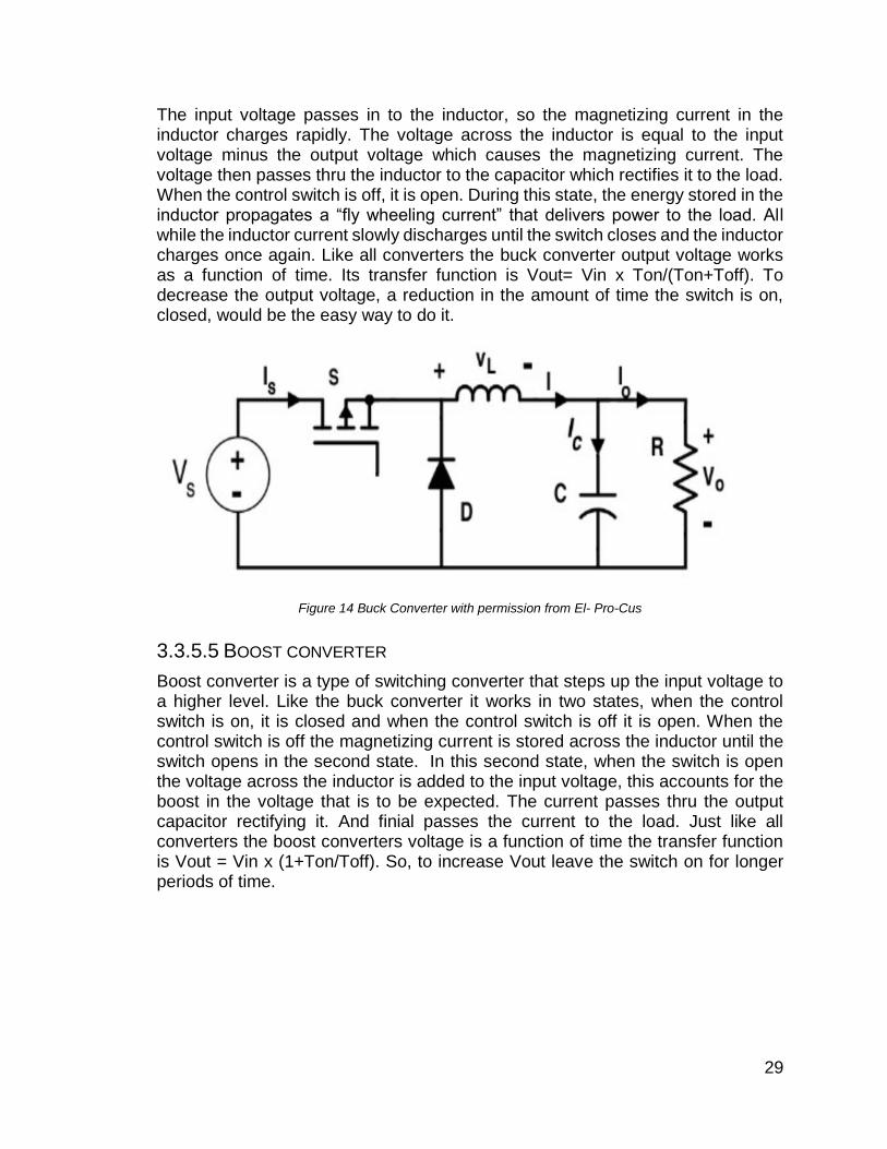
29
The input voltage passes in to the inductor, so the magnetizing current in the inductor charges rapidly. The voltage across the inductor is equal to the input voltage minus the output voltage which causes the magnetizing current. The voltage then passes thru the inductor to the capacitor which rectifies it to the load. When the control switch is off, it is open. During this state, the energy stored in the inductor propagates a “fly wheeling current” that delivers power to the load. All while the inductor current slowly discharges until the switch closes and the inductor charges once again. Like all converters the buck converter output voltage works as a function of time. Its transfer function is Vout= Vin x Ton/(Ton+Toff). To decrease the output voltage, a reduction in the amount of time the switch is on, closed, would be the easy way to do it.
Figure 14 Buck Converter with permission from El- Pro-Cus
3.3.5.5 BOOST CONVERTER
Boost converter is a type of switching converter that steps up the input voltage to a higher level. Like the buck converter it works in two states, when the control switch is on, it is closed and when the control switch is off it is open. When the control switch is off the magnetizing current is stored across the inductor until the switch opens in the second state. In this second state, when the switch is open the voltage across the inductor is added to the input voltage, this accounts for the boost in the voltage that is to be expected. The current passes thru the output capacitor rectifying it. And finial passes the current to the load. Just like all converters the boost converters voltage is a function of time the transfer function is Vout = Vin x (1+Ton/Toff). So, to increase Vout leave the switch on for longer periods of time.

30
Figure 15 Boost Converter With permission from El-Pro-Cus
3.3.5.6 BUCK BOOST CONVERTER
A boost buck converter is a combination of both a buck converter and a boost converter combined together at the inductor. It is used for when an input voltage needs to be either stepped up or stepped down. Because there are no less than two switches the converter will incur switching losses when the converter switches between boost and buck configurations. There is a total of four drivers, so the BOD will cost in both space and money. As stated earlier the buck and boost converters will be combined at the inductor. To stimulate a buck converter, the right most switch will stay open, allowing the left most switch to provide the buck operations. In the case of a boost converter the left most switch will stay closed in so that the right most switch can control the boost operations.
Figure 16 Switching Regulator with permission from Chegg

31
3.3.6 HEAT SINK
Heat sinks are the most commonly used thermal management systems in embedded designs. They are also the most basic. Heat sinks do not need any power at all and can be used on any device without exception. This makes it versatile and easy to use.[47] Heat sinks work by transferring dissipated power in the form of heat from the device generating the heat to the lower temperature medium. In most cases the lower temperature medium is air. Heat sinks are made of metals that have higher thermal conductivity values.
Heat sinks are designed to make the most use of the surface area in contact with the medium with the lower temperature. To do this heat sinks, utilize “fins” to allow the cooler medium to meet the heat generating element to cool down the embedded system faster. As stated earlier this is the most common thermal management system and requires no maintenance [47]. More advanced thermal management systems are used when designers need keep a device at a temperature other than room temperature.
3.3.7 BATTERY CHARGERS
Battery chargers work in three phases. The first phase only comes into play when the battery is critically under charged. This is when the battery charge must trickle charge the battery until it is within the acceptable range when the second phase can kick in. The second phase is the constant current phase. The current being applied to the battery is always supposed to be half of the current the battery can deliver. This corresponds to .5C of the batteries current. So 1C or just C would be the full current the battery can bring to bear. The constant current phase gets the battery to around 70-80% of the charge. This all happens very quickly. It is important to note that some battery chargers advertise that their products can charge twice as quick as their competitors, this is only because their products have a constant current mode and only charge to about 70-80% of the total charge. In order to get the full charge out of your battery, there must be a constant voltage mode, this is the more time intensive part of the charge. It is important to charge your battery to its full charge in order to preserve the longevity of the battery. it’s also important to note that lithium ion batteries need to be charged to within .1% of their total charge. Overcharging can damage the battery potentially causing it to blow up. In conclusion a constant current and constant voltage battery charger would be the better buy compared to just a constant voltage charger.
3.4 PART SELECTION
This portion of the report outlines what parts were selected for each individual module.
3.4.1 COMMUNICATIONS MODULE
The communications module for this device will consist of the following:

32
Transceiver Transmitter Receiver Switch (capable of Push-to-Talk) Antenna control Internal power Supply
RF amplifier Headphone Microphone Antenna
The Communications module is broken down into two sub-systems: voice communications and data communications. The goal for the Communications module is to provide both voice communications between two SARHesa units and broadcast their GPS locations back to a base station. The voice communications sub-system consists of one Arduino-based Microcontroller Unit (MCU) utilizing the ATMEGA2560 chip, and the nRF24L01+, which is a 2.4 GHz radio. The data communications sub-system consists of one Arduino-based MCU utilizing the ATMEGA328P chip, RFM69HCW radio functioning at 915 MHz, and a bi-directional logic converter. These mission critical sub-systems must be independent of one another. This design redundancy is a failsafe in case of communication failure.
Special considerations for choosing components for the voice communications sub-system were the processing capabilities of the MCU and the operating frequency of the radio. Due to a limited budget and FCC regulations on radio operators, the voice communications sub-system utilizes an Arduino-based MCU with the ATMEGA2560 chip and the nRF24L01+ 2.4 GHz radio. The reason the ATMEGA2560 chip is used is due to its processing capabilities, its market availability, and its cost-effectiveness. One important consideration to choosing the appropriate MCU is its processing capabilities, specifically whether or not it is equipped with an Analog-to-Digital Converter (ADC) that can handle the sampling for a walkie-talkie style device. A pro to the ATMEGA2560 chip is that its ADC is able to handle sampling audio at 8KHz, which is needed to produce telephone-quality speech. It comes equipped with a 16-channel, 10-bit ADC. For this line of MCUs, the estimated time it takes to read an analog input is 100 microseconds, with a max sampling rate of 10,000 times a second. The sampling rate is sufficient for the purposes of this project. Other advantages of the ATMEGA2560 chip is that it has dedicated Serial Peripheral Interface (SPI) ports needed for communications with the nRF24L01+ 2.4GHz radio. It has enough digital input/output pins and analog input pins needed for a walkie-talkie style circuit.
Due to FCC regulations, there are limited amounts of operating frequencies that non-licensed radios can operate on. Choosing the proper transceiver meant abiding by FCC regulations that limits which non-licensed frequencies can transmit voice. This is why a design for a digital walkie-talkie was favorable. The digital transmission over analog meant greater flexibility in choosing an unlicensed

33
operating frequency. The nRF24L01+ 2.4GHz radio was selected due to its market availability and price point. Other advantages are its Industrial, Scientific, and Medical (ISM)-band operating frequency and decent operating range, which is at 60 meters with clear line of sight. Its reliability and many readily available online resources make it a popular choice among amateur radio enthusiasts. FCC regulations on radio operation, specifically for voice transmission and receiving, are strict. The FCC often designate certain frequencies to emergency personnel and first responders. For the purposes of the SARHesa, the 2.4 GHz frequency, although quite susceptible to interference due to a number of other devices using the same frequency, is acceptable for the short-range voice communications demonstration.
Transmission of GPS data, latitude and longitude, to the base station is one of the project’s mission critical objectives. The transceiver must be reliable and robust. It must be under the sub-1 GHz frequency. It must be equipped with strong signal lock capabilities and range. The MCU must have fast processing capabilities and have enough ports for the integration of both the location module components and data communications components.
An Arduino-based MCU utilizing the ATMEGA328P chip was selected due to its market availability, price point, and ability to process the necessary data. Its high performance coupled with low power consumption made it a good choice as the MCU for the data communications sub-system. Advantages to the Arduino ATMEGA products are the amount of readily available online documentation and its strong online support community.
The RFM69HCW is a sub-1 GHz radio available at a wide frequency range. The radio module is available in 315 MHz, 433 MHz, 868 MHz and 915 MHz license-free ISM band. The 915 MHz range was chosen due to its availability for use in the United States for passive data transmission. Several of the key features about this transceiver are its high receiver sensitivity at -120 dBM at 1.2 kbps (kilobits per second), high power output capability at +20 dBM at 100 mW, and high dynamic Received Signal Strength Indicator (RSSI) range at +115 dB. The high receiver sensitivity, ultra-low power, and high RSSI range make it an ideal radio to send out GPS coordinates at predetermined intervals back to base station. Passively sending data means that considerations were taken to make sure that its power consumption was fairly low, since it will be utilizing the same battery pack as the Localized Location module, AV module and voice sub-system. Since the receiver on this transceiver is quite sensitive, it also meant that its RSSI range would be high. The RSSI value is indicative of how much power is being received by the radio factoring all the associated losses accompanying wave propagation. A higher range equates to a strong power signal. 5V is needed to power the Arduino-based MCU that the RFM69HCW is connected to. However, the radio is quite sensitive and any voltages above 3.3V will cause the radio to break. The function of the bi-directional logic converter is to act like a transformer to step down the voltage from 5V to 3.3V so that the radio can function properly.
3.4.1.1 TRANSCEIVER

34
Table 1 Transceiver Module Comparison
Feature Link TRM-XXX-
DP1203 TI CC1352R
Current Consumption (TX)
62ma at 15dBm 14.3mA(868 MHz)
Current Consumption (RX)
14mA 5.8mA(868 MHz)
Data Rate 153.2 kbps 125 kbps
Modulation FSK 2-(G) FSK
Operating Frequencies 433/868/925 MHz Sub-1 GHz and 2.4 GHz
Operating Temperatures
-45°C - 85°C -45°C - 85°C
Power Output 11dBm up to 14 dBm
Receiver Sensitivity -100 dBm -122 dBm
RF Family/Standard General ISM < 1 GHZ
General ISM < I GHz
Serial Interface SPI Multiprotocol
Size 30.5mm x 18.5 mm 7mm x 7mm RGZ VQFN48 (28 GPIOs)
Supply Voltage 2.4V-3.6V 1.8V-3.8V
The transceiver in this module will be capable of transmitting both voice and data from the GPS module. In the case of voice transmission, it will transmit voice data from one helmet to another. GPS data transmission will be from one helmet to the receiving base station. In the case of RF interference, this module doesn’t come equipped with frequency hopping agility but as an extended goal will be implemented on a with a microcontroller to better satisfy reliable communications requirement. The immediate goal of the transceiver module is to provide means for transmission and receiving capabilities. In the case of RF interference, two transceiver modules will be implemented, one operating in the 868MHz range and one operating in the 925MHz range, to enable frequency hopping for more reliable communications [14]. Specifically, the TRM-XXX-DP1203 is a radio frequency transceiver module operating in the 433, 868, or 915 MHz license-free Industrial, Scientific, and Medical (ISM) frequency band. This transceiver module has capabilities of high-speed data rate of up to 152.3kbps. The goal of the TRM-XXX-DP1203 module is to provide means for transmission and receiving capabilities. It modulates through Frequency Shift Key (FSK) meaning that it modulates through digital means. Information will be encoded digitally and will be transmitted through discrete frequency changes through the carrier signal [22].
3.4.1.2 RF AMPLIFIER
The primary function of an RF power amplifier is to take low power radio frequency signals and boost them to higher power signals [4]. The RF power amplifier may

35
do this by boosting either the radio frequency signal or the power at the input of the circuit [21].
Table 2 Amplifier Comparison Table
Feature Maxim MAX2235 Analog Devices ADL5530
Operating Feature 800MHz to 1GHz Variable up to 1GHz
Power Output up to 32.5dBM (at 5V) 10dBM per tone
Power Input +13dBM (20mW) +10dBM
Operating Voltage +2.7V -+5.5V 3V-5V
Power Control Range 37dB N/A
Efficiency 47% N/A
Power Gain 26dB 16.5dB
Noise Figure -90dB 3dB
Input VSWR 50Ω 50Ω
Power supply Current 315mA 110mA
at the input of the circuit [21].
The MAX2235 RF power amplifier is designed for operations within the 800Mhz – 1000Mhz range. At the 836MHz mark, the MAX2235 is capable of outputting a range from +28dbm at 2.7V to 32.5dbm at 5V. IT as a ramp with capabilities to power up or power down. The design intent with this RF amplifier is to work in conjunction with the antenna to boost the low-powered signals. Several important factors to consider when choosing which RF amplifier to integrate into the design are the following [4]:
Gain Power output Bandwidth Power efficiency Linearity Input and output impedance matching Heat dissipation
3.4.1.3 ANTENNA
The purpose of the antenna is for transmission and receiving a radio frequency’s signals. The size and design of the antenna can impact the device as it can enhance its range of transmission and receiving capabilities. A factor that must be considered when attempting to transmit and receive radio frequency signals are is the actual radio frequency itself. Generally speaking, the lower the radio frequency, the longer distance it can travel. The Ultra High Frequency range from 300MHz to

36
3GHz is ideal for this project as radio frequencies in this range are shorter waves, usually around 1 and a half feet and maneuver through things like buildings and doors better than radio frequency waves at the Very High Frequency range, which range from 30 MHz to 300 MHz However, the tradeoff is that signals at lower frequencies are also more susceptible to interference. A potential solution to this dilemma is to provide a clear, line of sight. The antenna can provide a solution to this by extending your range of communications by extending the line of sight. Another reason an antenna is a good solution to extension of communications is that by extending your antenna, you can extend the communications range without having to increase your power. Increasing the power for a communications module can be hazardous as it will emit electromagnetic fields at much stronger levels.
An immediate goal for the omnidirectional antenna needed for the communications module is to be able to communicate between the ranges of 0.5 miles to 2 miles. A reach goal for extending range would be to build transmitting and receiving repeaters. These repeaters will enable the communications module to expand its limited range by first acquiring the signal transmission on one frequency and then re-transmitting it on a very similar frequency [20].
3.4.1.4 MICROPHONE/HEADPHONE
Push-to-Talk or Push-to-Transmit (PTT) is a communications method that involves half-duplex communication lines. Half duplex communication is a way to transmit data one direction at a time. This means that while one person is transmitting a signal, multiple other receivers can pick up the signals at the same time. While transmitting the signal, the user cannot receive any signals himself/herself. The PTT button acts as a switch to toggle between transmit-mode and receive-mode.
An advantage to having PTT integrated into the microphone/headset for this communications module is that it enables only one user to speak at a time. This is particularly useful so that all users receiving will only be able to hear one transmitter at a time. The functionality follows the methodology of clear communications. An extended goal for this communications module’s peripherals would be to incorporate temple transducer technology to enable more clear speech.
3.4.1.5 SOFTWARE FOR COMMUNICATIONS MODULE
The main component of the communications module is the Texas Instruments CC1352P Microcontroller Unit (MCU). In order for this MCU to perform the tasks that it is designed to do, several software components will need to be involved. The following are the software needed for the Texas Instruments CC1352P:
• Texas Instruments SmartRF Studio
• Texas Instruments SimpleLink CCx2 Software Development Kit
• Texas Instruments RF Range Estimator
• Code Composer Studio
• OPUS audio codec

37
Texas Instruments SmartRF Studio is an application that interfaces with the low powered RF devices on the CCx2 series of microcontrollers [82]. This API configures and evaluates the microcontrollers and specializes in helping developers with the following:
• Configuration of register values and commands
• Practical testing, evaluation, and debugging of the RF system
It features link tests which enables the transmission and receiving of packets between nodes [82]. It is capable of antenna and radiation tests and setting the radio in continuous transmission and receiving modes [82]. It allows for customized GPIO configuration and allows for communication with the Launchpads and evaluation boards via USB [82].
Texas Instruments SimpleLink CCx2 Software Development Kit is a development environment specifically for the CCx2 line that helps in development of wireless and wired applications with Texas Instruments hardware[83]. It is composed of three parts:
1. Hardware – consists of ARM Core MCUs, radios, etc that support several connectivity stacks like sub-1Ghz, BLE, WIFI, Ethernet, Thread, Zigbee, Bluetooth, etc. [83]
2. Software - developed with code portability in mind so that code from one microcontroller for one connectivity stack and be implemented on another microcontroller on another connectivity stack [83]. Drivers for SPI, I2C, I2S, UART, etc are also included in this
3. Development tools/ecosystem – consists of launch pads, plugins, support, cloud development tools, training programs online [83]
The Texas instruments RF Range Estimator is a Microsoft Excel spreadsheet developed to help estimate the RF range for the project. It includes calculators for Line of Sight Range (LOS) and a Range Debug Checklist that takes a step-by-step approach to walking the user through achieving the maximum possible range for their RF device.
Code Composer Studio is the integrated development environment (IDE) that specifically is made for the Texas Instruments microcontrollers. It has many tools in it to help developers code, debug these embedded processors. This will be the main IDE used to program the CC1352P. The main code to be used will be in the language of C.
Opus audio codec is a royalty-free, open source, IETF standards-based codec that encodes and decodes audio. Since the CC1352P will be using an analogue to digital converter, the resulting signals will be digital. Those digital signals will need a codec, like OPUS, to encode and decode it. It will compress the and decompress the audio data so that it will be suitable for transmission through packets. It follows the Internet Enforcement Task Force (IETF) Standard and aims to enable interactive audio over the Internet [89]. As a background, the following must be fulfilled for the successful transmission of speech. Telephony uses frequency

38
bands ranging from 300 Hz – 3400 Hz. The frequency being used for the communications module is 433 MHz due to it being an unlicensed ISM band. The bandwidth allocated for single voice-frequency transmission channel is 4 kHz, including guard bands and allows a sample rate of 8 kHz per the Nyquist-Shannon Sampling Theorem [90].This audio codec is suitable for the communications module due to several factors. OPUS audio codec is open-source and free license for use. It allows a sampling rate of 8-48 kHz, ranging from both narrowband to full band. The sampling rate for voice is 48 kHz so this is codec is suitable to handle the task. It can handle bitrates from 6-510 kb/s. In digital radio, signal transmissions, the United States, for FM transmissions are at the rates ranging from 96 – 128 kbps with their carrier frequencies transmitting at 64 kbps. OPUS has bitrates from 6-510 kbps which is enough to handle the data rates needed for voice transmission. It also features mono and stereo outputs since it was specifically developed for speech and music support [89].
The communications module is fairly simple hardware-wise but does need quite a bit of software support to be able to achieve the task of sending and receiving clear, reliable communications between helmets and also to the base station. All of this software will enable the CC1352P to transmit and receive voice and GPS data from helmet-to-helmet as well as helmet-to-base station.
3.4.2 AUGMENTED VISION MODULE
The vision module has a simple task that it needs to perform: take a video stream from the camera and display it on the mini screen for the user. There are component level constraints that must be considered when picking components to ensure compatibility. Cameras have several data types that data is exported in and screens have specific ways they accept data. Screens and cameras both limit the resolution allowed. A low-resolution camera creates a small image on a high-resolution screen and a low-resolution screen either cannot display a high-resolution image or compresses an image into single pixels. Another constraint is the control unit or processor. If the controller or processor does not run fast enough there will be noticeable delays and buffer times.
There are two types of cameras often called IR cameras. The first is known as the IR camera or thermal camera. This camera picks up light waves emitted in the infrared spectrum. The other type of camera is called the NIR camera. This camera picks up light that falls in between the visible light and infrared light spectrum. The chosen camera for this project is the NIR camera. Many security and night vision cameras use the NIR camera due to its lower cost and better image resolution. NIR cameras can be used during high light and low light level conditions. In high light level conditions, it will output a colored image. At low light level conditions, the image will shift to a gray scale image. Furthermore, in low light level conditions, the wavelengths that the NIR camera receives falls in a very narrow band. The gray scale image is still transmitted in one of the color data types. The color data type used by the camera is the Blue-Green-Red (BGR) data type.

39
The camera selected is a small USB camera designed with an NIR cut filter and a clear lens. This allows the controller to switch between normal daylight filter and a lens that allows NIR light in when visible light is no longer strong enough to show a quality image. The camera is always kept in NIR mode; so the mechanical switch is removed from the filter, keeping the NIR cut-off filter off the sensor.
The Raspberry Pi is the control unit of the NIR camera. It is a complete computer measuring 85.6 mm by 56.5 mm. The Raspberry Pi is optimized to work with the Raspbian desktop. The Raspbian operating system is a Linux distribution, which allows easy version control across hardware. The screen attached to the Raspberry Pi is a Thin-Film-Transistor (TFT) display that displays in color.
3.4.2.1 DISPLAY SCREEN
The display screen will need to be a small screen that can be put in front of the user's eye when needed and removed from view when not needed. The display screen will take the input from the camera via the control module.
On the market today, there are a wide range of sizes for the display screen. They operate at 3.3V or 5V logic levels and typically use 3.3V for input voltage. Power for display screens is usually between 100mW and 500mW. The display screens use several communication protocols. Varying refresh rates depend on the model.
3.4.2.2 IR BEACON
Each helmet will need an IR beacon. This beacon will be an IR LED of some kind to allow others within line of site to be able to know where you are in the low light conditions. The camera will be able to detect the IR beacon and it will show up bright on the display screen.
On the market today, IR beacons operates at lower voltages 1.5V. They usually operate in ranges of 100 to 1000mA.
3.4.2.3 FILE STORAGE
The file storage system will need to record the user’s actions should they want that function. The two main types of file storage that will work at this size is SD and micro SD cards. A micro SD card works best with a smaller footprint and mass.
On the Market today, SD cards come in standard SD and microSD form factors. They normally operate at 3.3V logic levels. SD cards use the SPI communication protocol.
3.4.2.4 CONTROL UNIT
The control unit will need to be able to take the video feed from the camera module, record the feed to a data storage device such as a SD card, display the feed on a display screen for the user, and display added information on screen extrapolated from the feed itself and from other components on the board.

40
There are several types of control units available today. The most common type of control units are microcontrollers, microprocessors, system on a chip (SoC) and, field programmable gate arrays. The lines delineating the difference between microcontrollers, microprocessors and, SoCs are blurry. Typically, a microcontroller has the slowest of the three options. Over the past few years microcontrollers have become faster and can compare with microprocessor clock speeds. Likewise, SoCs have been integrating multiple microprocessors as part of the chip design which while does not increase clock speeds, it does allow the SoC to do more at the same chip size. The other major difference between the three options is memory. Microcontrollers have the smallest amount of memory, often just enough to hold a program and program variables along with a data buffer or two. Microprocessors have more memory and SoCs have even more memory or have memory options available on board for it to utilize. The final option is an FPGA it is unlike the other three options as it does not utilize the same approach. The FPGA uses logic blocks in order to define the code. The speed of an FPGA board is defined by the complexity of the code as the major restricting factor is propagation delay.
3.4.3 LOCALIZED LOCATION MODULE
The goal of the Localized Location module is to provide coordinate data of the SARHesa user to the Communication and Augmented Vision modules. The main components of the Location module are the NEO-6M GPS module and the ATmega328P microcontroller, shared with data communications. GPS is the chosen location technology for the SARHesa, because it is the most reliable and cost effective for SAR operations. GPS receivers have accurate time and position, because of the process of trilateration that uses the GPS’ network of approximately 30 satellites orbiting the Earth[7]. Using Wi-Fi, which uses a network of devices, would not be reliable for SAR team members, who perform operations in buildings with failing infrastructures and outdoors due to the Wi-Fi access points requiring power to operate. Using Beacon technology would reduce power consumption and have good data speeds. However, it would be ineffective because multiple beacons would have to be stationed in specific spots at the time of SAR operations with sensors that would pick up the beacon signals. Using Radio Frequency Identification (RFID) technology is expensive, is for short range use, and often requires user interaction to operate. Using Near Field Communication (NFC), though inexpensive, is very short range only [6].
The Localized Location Module uses a Neo-6M module. The Neo-6M module runs on 2.6V to 3.6V, which is within the range of most readily available batteries. This has an advantage over other GPS receivers that operate at higher voltages, which would need more power infrastructure to step up the voltage. The National Marine Electronics Association (NMEA) protocol baud rate is 9600 bps for the Neo-6M module when CFG_COM0 and CFG_COM1 are both set to 1. The Localized Location module needs to lock an accurate localized location in as little time as possible during a SAR operation. The Neo-6M accomplishes this; with a hot start

41
of 1s with a sensitivity of 156dBm, and a cold start of 27s with a sensitivity of 147dBm. It has three configuration pins and 1-time pulse[1].
The ATmega328P microcontroller is used for Localized Location module of the SARHesa. The Neo-6M connects to four pins on the MCU: GND, 3.3V, and two pins for Transmit and Receive . Reference designs for the Arduino Uno microcontroller board were used to create an Arduino with the capabilities needed for this project. For example, an external 16MHz crystal oscillator is used to set the clock frequency of the MCU.
Another note for hardware for the Localized Location module, is that the Future Technology Devices International (FTDI) is used to configure the Neo-6M module. A microcontroller is needed to send information to the inertial measurement unit to the GPS to the Communication Module. The Atmel line of microcontrollers were considered and researched, because of their use on the Arduino Uno and Arduino Nano. The products in the Arduino family was a great place to start research, because of the many sources available for use of Arduino products.
3.4.3.1 ARDUINO UNO
3.4.3.1.1 ARDUINO UNO The Arduino Uno was taken into consideration, because there are thousands of projects that are based on this board, making this microcontroller a great reference tool. The Arduino Uno is based on the ATmega328P. The Arduino Uno is made so that it can be expanded with different shields. The Arduino Uno has 14 digital I/O ports, 6 of which are pulse with modulation(PWM) for dimming LEDs and step remote, and 6 analog inputs. A USB port allows the Arduino Uno to communicate with another deice and to connect to a power supply. The Arduino Uno also has a power connector that can be used for a project that is battery run or a wall use with a wall mounted power supply. Testing the Arduino Uno is straight forward, because there are a series of connectors that it has, to plug jumper wires into. Ultimately, the Arduino Uno has capabilities that are not of necessary for the safety and rescue helmet. The microcontroller used needs to be as light as possible[49].
3.4.3.1.2 ARDUINO NANO The Arduino Nano is just as powerful as the Arduino Uno, maybe even more so, having two more analog input pins. Having the same number of I/O pins as the Arduino Uno, the Arduino Nano is of a better size for smaller projects. Unlike the Arduino Uno, the Arduino Nano is powered using a USB mini port, cannot be used with Arduino shields, must be wired, and its pins must be soldiered to allow it to be plugged into the board. When prototyping, jumper wires cannot be used. The Arduino Nano would have to attached to a breadboard, which could potentially mess up contacts on the breadboard and would prevent the breadboard from accepting wires. Some other ways to test the Arduino Nano would be to use male and female cables, or, the better way, using prototyping boards. The smaller the microcontroller, the better for the safety and rescue helmet[49].

42
3.4.3.1.3 ARDUINO PRO MINI The Arduino Pro Mini departs from the Arduino Uno and Arduino Nano, having no USB port. Instead it uses a FFDI adaptor to program and charge the Arduino. This would be ideal for projects that only need to be programmed once. It has the same number of Digital I/O pins as the Uno and Nano. The Arduino Pro Mini, that normally runs on 5V, can run on 3.3V to save power. The con would be that it would run at half the speed. This Arduino has no components on the bottom side and will fit perfectly onto a printed circuit board. This was a contender for the microcontroller choice, because little power needs to be used and the location module must be small[49].
3.4.3.2 ATTINY85
The ATtiny85 is, while not an official Arduino board, a very small Arduino The ATtiny85 is great for battery powered projects. The ATtiny85 does not have a lot of I/O ports. The ATtiny85 is used when little current is wanted to be used. It’s powered using a micro USB or 5V pin. It may need different drivers, depending on different operating systems, which is not ideal, when wanting ease in use[49].
Table 3 Microcontroller Comparison_1.
ATmega328P ATmega2560
Cost $2.14 12.35(Digi key)
Pin Count 28-32 100
MAX I/O pins 23 86
Flash Memory(Bytes) 32K 256K
EEPROM(Bytes) 1K 4K
ADC channels 8/UNKNOWN 16
PWM channels 6 15
Timers 2 8-bit timers , 1 16-bit timer 2 8-bit timers, 4 16-bit timer
SRAM(Bytes) 2K 8K
Hardware Serial YES-1 YES-4
Hardware I2C YES YES
External Interrupts 23 PCINT/UNKNOWN UNKNOWN
3.4.3.3 ATMEGA328 CHIP
The ATmega328 chip allows for the same capabilities as the Arduino family, but with the use of less current and a lighter package. It has 14 I/O pins, 6 of which are PWM, and 6 analog inputs. Minimal parts are required to successfully use the ATmega328 chip. With a crystal the chip will run at 16MHz and 8MHz without. This is a perfect for making the localized location module as light as possible with the same capabilities of the Arduino Uno. The ATmega328P will be used when creating the custom printed board circuit for the Safety and Rescue Helmet [49].
Table 4 Microcontroller Comparasion_2

43
ATtiny2313 ATtiny84 ATtiny85
Cost $1.64 $2.05(Mouser) $1.24(Digi key)
Pin Count 20 14 8
MAX I/O pins 18 12 6
Flash Memory(Bytes) 2K 8K 8K
EEPROM(Bytes) 128 512 512
ADC channels 0 8 4
PWM channels 4 2??? 2???
Timers 1 8-bit timer, 1 16-bit timer
1 8-bit timer, 1 16-bit timer 2 8-bit timers
SRAM(Bytes) 128 512 512
Hardware Serial NO NO NO
Hardware I2C NO NO NO
External Interrupts 8 PCINT 12 PCINT 6 PCINT
3.4.3.4 ATTINY85 CHIP
The ATtiny85 chip is great to use for simple projects because no other parts are needed. It has less I/O ports than the ATmega328 chip, having 6 multipurpose I/O pins. However, this chip is good for building final circuit boards for battery powered projects that do not need a lot of memory. This chip is not the best choice for this project, because we would need more pins to connect to the GPS, MEMS, and communication devices [49]
Table 5 Microcontroller Comparasion_3 [120][121]
MSP423E401Y
Cost $16
Pin Count 43
MAX I/O pins UNKNOWN
Flash Memory (Bytes) 1024KB
EEPROM 6KB
ADC channels 20
PWM channels 8
Timers 8 timers
SRAM(Bytes) 256KB
Hardware Serial UNKNOWN
Hardware I2C YES- 10
External Interrupts UNKNOWN
3.4.3.5 ACCELEROMETER

44
An accelerometer function is axis-based motion sensing [6]. An accelerometer has a sensor made of microscopic crystal structures that give an output voltage when stressed due to accelerative forces. The accelerometer interprets the output voltage to find the direction the object it is pointing in [6]. Short term movements can be tracked, because the accelerometer keeps track of direction due to gravity [9]. We want the safety and rescue helmet to conserve as much power as possible, during search and rescue missions. Accelerometer-only data helps conserves power in devices that log a lot of data [8].
3.4.3.6 GYROSCOPE
Most accelerometers are limited to what they track and are not consistently accurate [8]. Adding a gyroscope to an accelerometer allows distance travel without user input [8]. A gyroscope measures the rotation or angular velocity of an object [13]. It provides information about the accelerometer in all directions and rotations around each axis [9]. Emotiv Inc., a bio-informatics and technology company, emphasizes that the addition of the gyroscope helps accurately maintain both the instantaneous and long-term earth frame reference for gravitational and linear accelerations [8]. Gyroscopes have been used in short term full-space head tracking for video game devices [9]. Gyroscopes have also been used in tracking the distance traveled by a runner to find their way back home [9]. Keeping track of the distance of our rescue team member to get him or her back to the home base could be a very useful feature in our safety and rescue helmet.
3.4.3.7 MAGNETOMETER
A magnetometer, combined with the accelerometer and GPS, tracks real position and orientation in space [9]. A magnetometer is an instrument used for measuring magnetic forces, especially earth’s magnetism [12]. It measures the direction, strength, or relative change of a magnetic field at a location. The compass is a type of magnetometer, which is a significant reason to include it in our safety and rescue helmet. A phone, for example, will use the magnetometer with the data from its accelerometer and GPS to calculate the whereabouts of the phone’s user [6].
3.4.3.8 GLOBAL POSITIONING SYSTEM TECHNOLOGY (GPS)
A GPS will use the accelerometer, gyroscope, and magnetometer in locating an object. A GPS will use the information from these sensors, sending pings to satellites, to calculate where the object is based on the angles of intersection [6]. A GPS does drain battery from communicating and calculating [6]. This will have to be kept in mind when writing the software and choosing the power source for the safety and rescue helmet design.
The Global Positioning System(GPS) is a network made up of 30 satellites that orbit the Earth at an altitude of 20,000 km according to the article “How GPS Works.” The GPS used to be for only military use, but it now available to any GPS device. The GPS device receives radio signals from the satellites to locate the position that it is at. At least four GPS satellites are visible wherever you are on the

45
planet. Each of the GPS satellites send information about its current position and time at regular intervals. The GPS satellites send signals at the speed of light. The signals are intercepted by the GPS receiver (the device), that will calculate how far away each GPS satellite is based on how long it took the signals to arrive. The GPS uses trilateration to find location. Trilateration finds location from the point where the three spheres, the GPS satellites, intersect. The information of the distances of the three or more GPS satellites is processed by the receiver, to perform trilateration [60].
The GPS satellites have atomic clocks to keep accurate time. There is a difference in clocks in space and on earth, because of general relativity, which predicts that time will appear to run slower under stronger gravitational pull. The clocks board satellite will run faster than the clock on Earth. The GPS network compensates for this type of discontinuity [60].
3.4.3.9 MEMS
The accelerometer measure acceleration by measuring change in capacitance. In the accelerometer, mass is attached to a spring. When acceleration occurs in a direction, mass will move the capacitance between the blades surrounding the mass, changing the mass, giving a particular acceleration value[50].
The gyroscope measures the angular rate. A mass is constantly moving, oscillating, the angular rate will cause mass to move and make a perpendicular displacement [50].
The magnetometer measures the magnetic fields strength and direction. The magnetometer has a magnetic plate where electrons move equally from one side to the other, until there is a disturbance in flow. When there is a disturbance in flow, the electrons go to one side of the plate. If you put a meter on either side of the plate it would give a voltage for the magnetic field strength and direction. This is called the Hall Effect [50].
3.4.3.10 FOG VS MEMS
An Inertial Navigation Systems(INS) had to be chosen for the Localized Module for the Safety and Rescue helmet. The two INS researched were the Fiberoptic gyroscope(FOGs) and the Micro-Electro-Mechanical Systems(MEMS). The research from the article "INS Face Off MEMS versus FOGs" made clear the advantages and disadvantages of both of the INS gyroscopes when utilized in an INS device [62].
Navigation technologies incorporated FOGs as the core device. Today MEMS is conforming to the most prominent device in the markets and operations that were first monopolized by FOGs. Many motion applications are using MEMS. The article mentioned an example of the use of MEMS, where the abrupt shifts in acceleration triggered safety systems. Research has already proved that MEMS is now heavily used in phones and gaming devices. The MEMS adjusts where the screen is facing or how the end user interplays with the device. Since a few years before 2012,

46
"MEMS has improved error characteristics, environmental stability, increased bandwidth, and increased availability of embedded computational power that can run advanced fusion and sensor error modeling algorithms [62]."
The changeover from FOGs to MEMS is clear in array stabilization operations. Antenna array stabilization in the past was ineffectual to mainly static operations where it was necessary to have a specific approach. Antenna array stabilization grew toward systems anchored inside land vehicles. These land vehicles existed primarily for military communication systems, disaster monitoring systems, and high-priced media communication systems [62].
MEMS is significant in the advances in two-way communication it is achieving. MEMS allows communication between Unmanned Aerial Vehicles(UAVs) and ground assets, streaming satellite TV to a vehicle in a city, or streaming video from a toy helicopter to a hand-held controller screen. MEMS is being utilized to create products that use directional antenna arrays [62].
FOGs technology is being replaced by MEMS in some of the following : machine control, precision agriculture, vehicle navigation advanced driver assistance systems, unmanned ground/aerial/submersible vehicles. FOG navigation is expensive compared to MEMS navigation. Some companies have paid up to $30,000 for FOG ,compared to the $500 for MEMS. This is done because the FOG is twenty-times more precise and is more reliable [62].
A INS system that costs significantly less than the pricey FOG systems is the Global Navigation Satellite System(GNSS). The GNSS involved multi-antenna systems for attitude measurement to achieve the same effect as the FOG systems. The multi-antenna systems have more hardware. Therefore, they are more costly than single antenna systems. However, the cost of a multi-antenna systems saves more money than purchasing FOG based INS/GNSS [62].
Agriculture products that incorporate MEMS and multi-antenna GNSS are going to create crops that give the more expensive FOG INS/GNSS Systems a run for their money. The cost of MEMS sensors are staying at a below average price because GPS navigation units that are built into the dashboard of a car are making use of current MEMS inertial sensors. Another device that took on MEMS was the Portable Navigation Device(PND). PNDs were money constrained. This helped bridge the gap between GPS outage problems that occurred when a vehicle drove through tunnels or parking garages. However, automatic dead reckoning, defined as calculating one's current position by using a previously determined position and advancing that position based upon known speeds over elapsed time and course, is being developed in vehicle navigation with MEMS. Because of this FOG systems are still needed as a reference system. The MEMS is a much more valuable option for devices that need to shortened power and payload needed to be used. Military ,aerospace, and commercial are gravitating to MEMS. according to the article "systems with a limited supply of power and payload are hardest to navigate with low cost INS because they are often designed for high dynamics and to operate for long periods of time without absolute navigation help such as from GNSS [62]."

47
The article analyzes two INS/GNSS systems. One with the FOG gyroscope and one with the MEMS gyroscope. Both navigation systems used the same MEMS accelerometer, MEMS barometer, and software integration filter. The main things that were compared were the bandwidth(Hz), bias instability(deg/hr), and the angular random walk(deg/sqrt(hr)) [62].
The MEMS gyroscope and accelerometer picked for MEMS GNSS system were some of the best parts among their competition in their price bracket. The key features looked at were: bias stability, orthogonality, g-sensitivity, and bandwidth. The hang-up of the MEMS gyroscope system is that it does not have the large valued bandwidth that is needed. The MEMS accelerometer does offer a high bandwidth, unlike the MEMS gyroscope that has a low bandwidth of 100 Hz or less. A low bandwidth is okay for regular vehicle navigation; but the MEMS gyroscope will struggle to keep up with rough off-road movement. When put in non-ideal conditions, the MEMS gyroscope can cause a high level of noise, which is not good. Luckily, For the GNSS-MEMS system discussed in this article, the MEMS chosen for this system balanced stability, noise, linearity, and linearity sensitivity, because they designed the system with multi-core architecture [62].
To compare the performance a FOG gyroscope the In Run Bias Stability(IRBS) technique is use. The IRBS technique tells if the gyroscope has a low inclination to change over a clear-cut span of time. Unfortunately, this technique cannot be used to reliably check the MEMS gyroscope units. The IRBS technique can only be used for static motion detection for the MEMS gyroscope. Keeping that in mind, this puts more importance on bandwidth and cross-axis sensitivity for multi-axis designs. Moreover, linearity sensitivity, the measurement of diversion from the slope of the calibration curve, defined as the quantity wanted as a function of values of sensor output, is an important determination that MEMS gyroscopes are not good at achieving consistently [62].
The MEMS gyroscope used for the GNSS-MEMS system was a resonator that was fully differential, having differential inputs and differential outputs. The MEMS gyroscope was being decreased to a highly linear region, where the device is not fully on or fully off, which leads to less vibration. A MEMS gyroscope combined with a accelerometer and multi-axis IMU normally leads to the system being off by 2 percent. However, the GNSS-MEMS system built only was incorrect by 0.087 percent. The low error was consistent over different temperatures, because of device specific determinations [62].
Accessible bandwidth and its capability to phase match, have a specific range of frequencies, across the axis is important to multi-axis designs. Gyroscopes can a bandwidth that correlates to decreasing noise; while other gyroscopes may have too small of a bandwidth, because of sensor processing in feedback electronics. Limitations such as this can cause additional phase-analogous errors that then effect the sensor signal path. In the built GNSS-MEMS the MEMS IMU provided a well proportional avenue to lessen the total determinants of the errors [62].
The FOG was chosen based on price, bandwidth, size, bias stability, and noise level. FOGs have better bias stability and significant improvement of angular

48
random walk, a specification for rate sensors, measuring the rotation rate about the devices axis, in comparison to the MEMS [62].
After testing, the FOG system was marginally better than the MEMS system. This was only by 5 percent when the vehicle was on pavement. On the off-road test, the FOG had superiority in a changing setting, with rough conditions, such as bumps, “fish tails” around corners, wheel spinning. FOG maintained its RMS accuracy between paved and off road, while MEMS declined between paved and off road [62].
FOGs 1000 Hz bandwidth is way better in comparison with MEMS 330 Hz bandwidth. However, the bandwidth for MEMS is more than enough to maintain 0.15 degrees certainty, excluding intense off- road driving. FOGs have superiority because of the increased bandwidth and lower noise [62].
The next test compared GPS and the two systems with GNSS multi-path outages, looking at the position results. The GPS had long signal outages when the vehicle was moving through downtown, where there are a lot of tall buildings. When the receiver gained a signal lock, its position shown was incorrect by ten meters. The GNSS-FOG showed a route within 5 meters of location certainty the entire distance traveled. The GNSS-MEMS did well in the downtown area populated by tall buildings as well. The maximum error was of 9 meters. Both the GNSS-FOG and GNSS-MEMS were considerably better than the GPS. Also, the GNSS-FOG and GNS-MEMS compared well to each other, considering how much more expensive the FOG is to the MEMS. Attitude root-mean-square(RMS), the effective voltage or current of an alternating current(AC) wave, outcome was 0.4 degrees off where there was an area populated with tall buildings. Heading Error RMS, the difference between the values found in the model, was 0.25 degrees for FOG, compared to 0.39 degrees from the MEMS. The roll and pitch error RMS, the difference of the average readings on the positions of the device and the distance between the different positions, values were nearly equal for both the FOG and MEMS. For multi-path schemes, position and attitude result for both MEMS and FOG were similar, which makes it hard to defend spending lots of money on FOG when you can get the cheaper MEMS and having the same normal driving conditions [62].
Ins-Only Navigation Test drove both vehicles at 12 kilometers. The vehicle with FOG showed a drift of 750 meters after 20 minutes. The MEMS showed a drift of 900 after 20 minutes. Both vehicles were without GPS updates and traveling off road the entire time. The FOG is better in roll and pitch certainty. The position drift was 20 to 30 percent better for the FOG. Moreover, there is two-times upgrade for roll, pitch, and heading for the FOG. The reason FOG is better, is because the MEMS system has some turn on biases that are not perfectly repeatable and do not require some outside help to remove their effects [62].
MEMS helps reduce the drift error of the heading gyroscope, while the accelerometer provided some weak instability to the roll and pitch gyroscope bias errors. Unfortunately, some underestimated biases do remain in the MEMS composition that make the results for attitude worse than for the FOGs. MEMS can be used for greater cost savings and with littler decline of effectiveness in many

49
cases. According to "INS Face Off MEMS versus FOGs" these devices include unmanned aerial and ground vehicles, precision agriculture control and guidance, in-dash navigation systems, antenna array stabilization systems on moving platforms, earthworks navigation equipment, and mining truck navigation and safety [62]. FOGs are still good for high accuracy mobile mapping systems, life critical military operations in hostile environments, and high dynamic/ vibration applications that need higher bandwidth according to the article "INS Face Off MEMS versus FOGs". In 10 to 15 years the article estimates that new technology will probably replace MEMS [62].
3.4.3.11 STRATEGIC COMPONENTS AND PARTS FOR LOCALIZED LOCATIONS
MODULE
The parts for the localized location module will be ordered from Mouser, Digi key, and Spark fun for their dependability on past projects.
3.4.3.11.1 Copernicus II GPS Receiver The Copernicus II GPS Receiver is a complete 12-channel GPS receiver. This GPS receiver provides the position, velocity and time data to the user through one of the three protocols of their choosing. Two of the Trimble’s protocols, the TSIP protocol and the TAIP protocol, could be of most use for this project. The TSIP protocol would be useful for the safety helmet because it “offers control over receiver operations and provides detailed satellite information,” according to the Copernicus II GPS Receiver datasheet. The TAIP protocol (ASCII protocol) is used for track and trace applications. To assure the safety of the operator of the helmet, having a tracker on the helmet would be vital, making the TAIP protocol another valid choice [20].
Table 6 GPS Comparison [23]
Feature JF2 Module GPS
Receiver Trimble Copernicus II GPS
Receiver
Power Consumption N/A 44mA(132mW) at 3V
Hot Start 1s 3s
Cold Start <35s 38s

50
Standards/Protocols NMEA and OSP NMEA
Tracking -163dBm -160dBm
Channels 48 12
Operating Temperatures -40°C to 85°C -40°C to 85°C
Accuracy (speed) <0.01 m/s N/A
Power Supply 1.75V - 1.9V -0.3V to 3.6V
Connections N/A surface mount
Serial Interface UART, SPI, I2C TSIP,TAIP
Size 11mm x 11mm x 2.6mm 2.54 mm T x 19mm W x 19 mm L
Supply Voltage 1.7V–1.9V 1.8V-3.8V
3.4.3.11.12 ICM -20948: low power 9-axis MEMS Motion Tracking Device The ICM- 20948 is an attractive part for the safety and rescue helmet, because it is suited for Wearable Sensors. This 3mm x 3mm x 1mm device contains the 3-axis gyroscope, 3-axis accelerometer, 3-axis compass (magnetometer), and a Digital Motion Processor that will collect information about the whereabouts of the safety and rescue helmet, that will be sent to the GPS receiver [7].
Table 7 IMU Comparison Table
Feature TDK InvenSense ICM-20948 Bosch Sensortec BMF055
Sensor Type Accelerometer, gyroscope Accelerometer, gyroscope
Output type I2C, SPI Digital
Operating Temperatures -40°C to 85°C -40°C to 85°C
Mounting type Surface SMD/SMT
Acceleration ±2g, ±4g, ±8g, ±16g ±2g, ±4g, ±8g, ±16g
9-axis 3.11mA N/A
Size 3mm x 3mm x 1mm N/A
Supply Voltage 1.7V–1.9V 2.4V to 3.6V
Gyroscope Only(low power mode) 1.23mA N/A
Accelerometer Only(low power mode) 68.9µA N/A
Magnetometer Only 90µA N/A
3.4.3.12 SOFTWARE
There are three types of interfaces that can be considered to communicate between the different parts of the localized location module: UART, I2C, and SPI.

51
3.4.3.12.1 UART
Universal Asynchronous Receiver/ Transmitter (UART) is asynchronous, which means it does not have a clock. Therefore, all the devices must have the same baud rate, the same signal changes, to compensate for a lack of not having a clock. The baud rate is always between 1200 to 115200 bps. UART cannot have multiple devices on the UART bus. UART is also significantly slower than SPI. However, UART is a little bit more versatile than SPI in sending information to another device. UART bus starts at idle, until a start bit is sent. Next the data is sent. A parity bit can be sent to check errors. Lastly, a stop bit turns the UART bus back to idle
mode. UART will ultimately be the main protocol for the GPS [61]. Universal
Asynchronous Receiver/ Transmitter (UART) is asynchronous, which means it does not have a clock. Therefore, all the devices must have the same baud rate and the same signal changes to compensate for a lack a clock. The baud rate is between 1200 to 115200 bps. UART cannot have multiple devices on the UART bus. UART is also significantly slower than SPI. However, UART is a little bit more versatile than SPI in sending information to multiple devices. UART bus starts and stays at idle, until a start bit is sent. Next, the data is sent. A parity bit can be sent to check for errors. Lastly, a stop bit turns the UART bus back to idle mode. The UART protocol is used for communications between the NEO-6M module and the ATmega328P MCU, and the ATmega328P MCU and the AV module[3].
3.4.3.12.2 I2C
I2C consists of two wires that allow a master device to communicate to multiple slave devices, using 7-bit addressing. The Serial Data (SDA) is the data carrier and the serial clock (SCL) syncs data transfer between the master and slave from the master. An active low voltage is put across both lines. The data sequence is sent in 8-bit sequences. First the master sends the data to the slave addressed to. The slave device acknowledges whether the data from the master was received, with 1 bit. The internal register address then sends a data sequence until all the data is sent. The stop condition is the 8-bit that determines reading or writing [52]. I2C consists of two wires that allow a master device to communicate to multiple slave devices, using 7-bit addressing. The Serial Data (SDA) is the data carrier and the Serial Clock (SCL) syncs data transfer between the master and slave from the master. An active low voltage is put across both lines. The data sequence is sent in 8-bit sequences. First the master sends the data to the slave it is addressed to. The slave device acknowledges whether the data from the master was received, with one bit. The internal register address then sends a data sequence until all the data is sent. The stop condition is the 8-bit that determines reading or writing. I2C is the protocol used for communication between the MEMS and the ATmega328P MCU [4].
3.4.3.12.3 SPI

52
SPI consists of 3 wires and 1 chip select wire. The Master Out Slave In(MOSI) wire sends data to the slave device. The slave then send data back using the Master In Slave Out (MISO) wire. First the chip select is set on the slave device you are going to use. A command is sent to send out the data. Lastly, the decision is made to read or write data. The device that the master is communicating with is turned to active high. SPI is the interface that will be used because the project team is most familiar with it and it faster than if I2C were used. The disadvantage of using SPI is having a chip select line [58]. SPI consists of three wires and one chip select wire. The Master Out Slave In (MOSI) wire sends data to the slave device. The slave then sends data back using the Master In Slave Out (MISO) wire. First, the chip select is set on the slave device that is being used. A command is sent to send out the data. Then, the decision is made to read or write data. The device that the master is communicating with is turned to active high. The disadvantage of using SPI is having one chip select line per device; multiple devices cannot simultaneously communicate with the master. SPI is the protocol used for communication between the ATmega328P MCU and both onboard radios [5].
3.4.4 POWER MODULE
The following section outlines the power module and its associated components. The battery pack will serve as the power source for the SARHesa. The battery type chosen for this project is the Lithium-ion (Li-ion) battery chemistry. It is very important to choose a battery chemistry that is well suited for embedded type of applications. The Li-ion battery chemistry has a higher self-discharge rate when compared to its chief competitor, the Nickel Metal Hydride (NiMH) battery chemistry. Due to its higher self-discharge rate, it is well suited for the low current applications needed to power the devices on the SARHesa. The Li-ion is also smaller and can deliver higher voltages per cell. This is due to its recharging cycle being four times faster than NiMH batteries. The Li-ion battery is more resistant to varying temperatures ranging from cold environments to much hotter ones. Lastly, Li-ion batteries have a higher energy density, meaning that it carries more charge per gram than a NiMH battery of the same weight.
The SARHesa is meant to be worn by the user so weight and size are very important factors. In addition, the product was designed to be as user friendly as possible. It is intended for the batteries to be interchangeable. The 18650 Li-ion Battery was chosen because it is so common and easily found from reputable vendors on the Internet. The 18650 battery type takes approximately four hours to charge and varies very little across manufacturers.
The battery charger will charge the battery. Battery chargers work in three phases. The first phase occurs when the battery is critically undercharged. This is when the battery must trickle charge until it is within the acceptable range for the second phase to kick in. The second phase is the constant current phase. The current being applied to the battery should be half of the current the battery can deliver. This corresponds to the discharge rate, 0.5C, of the batteries current. This means that one cell will charge or discharge in two hours. The constant current phase charges the battery to 70-80%.

53
It is important to note that some battery chargers advertise that their products can charge twice as quickly as their competitors. This is only because their products have a constant current mode and only charge to about 70-80% of the total charge. In order to get the full charge out of a battery, there must be a constant voltage mode. This cycle is done in order to preserve the longevity of the batteries. It is also important to note that Li-ion batteries need to be charged to within 0.1% of their total charge. Overcharging can damage the battery, potentially causing it to blow up. Ultimately, a constant current and constant voltage battery charger would be the better choice compared to just a constant voltage charger.
The selected battery charger for the SARHesa is the BQ25606. It is a battery module that will charge the battery with 92.5%-charge efficiency. It is designed to be used with Li-ion single cell batteries. It works in conjunction with the 18650 single cell Li-ion batteries used in the SARHesa. It supports USB On-The-Go (OTG) applications. It also has a high battery discharge rate.
3.4.4.1 PHOTOVOLTAIC CELLS
All of the cells are monolithic and have efficiencies ranging from 17%-18%. All solar cells are sold from US manufactures and can be shipped under 1 month.
Table 8 Photovoltaic Cells Comparison table
Part # Mini Solar Cells P-Maxx-3500mA MC7815CTG
Manufacture Aoshike Silicon Solar Inc. Alyima
Voltages .5V 0.55V 0.5
Output Current 0.4A 3.5V 0.34
Wattage .02W 1.93W .17W
Dimensions 52 x 19 mm 15.6cm x8.4cm 39mm x 26mm
Cost $15.00 $1.00 $8.27
Quantity 100 10 20
3.4.4.2 SEQUENCERS
This next section outlines sequencers for the power module.
3.4.4.1.2 .1 LM3380
This sequencer is the easiest chip available from TI for controlling power up and power down sequencing of multiple different voltage rails. What a sequencer does, is stagger the startup and power down sequence to avoid large currents that make harm the entire system. This is a 6-pin package, three of the pins are dedicated open drain output flags, and one of the pins is the enable pin. Once the enable pin

54
has been activated the output flags will sequentially allow current to flow in a timed regulated manner. This will allow the device, the FPGA, to start up without risk of damaging it. When powering down, the output flags follow the reverse sequence order to avoid latch problems. This sequencer is very small, its input voltage ranges from 2.7V to 5.5V, which is of the same order of magnitude as another component’s in the design. The timing options are of standard values, and its operating current is very low at 25uA. Although this sequencer is specifically designed for automotive applications it will work fine for the purposes of this project.
3.4.4.1.2.2 LM3881
The LM3881 works in the same way the LM3380 does. The only relevant difference is that the time delay is adjustable unlike its sister product the LM3880. Because the LM3881 time delay is adjustable the its operating current is slightly higher at 80uA.
3.4.4.1.2.3 LT1371
The LT1371 is an adjustable switching regulator. It can be operated in all of the common switching configurations. These configurations include boost, buck, fly back, and forward. It has a high switching current at 3A, which accost for its high price tag. Its minimum input voltage is low at 2V, which is low enough to be able to take charge directly from the battery without having to use a step up voltage regulator from the battery to the regulators sending voltage to the rails.
3.4.4.1.2.24 LT1371
The LY1108 is an adjustable switching regulator as well. Its output current is at 800mA, which Is enough to supply the correct amount of current to both the 3.3 and 1.8 V rails. The voltage needed to use the regulator is low at 2.7 volts.
Table 9 Switching Regulator Comparison Table
Type LM3881 LM3880 LT1108 LT1371
Vin (Min)(V) 2.7 2.7 2V 2.7
Vin (Max)(V) 5.5V 5.5V 12V 30V
Iout 100mA 500mA 800mA 3A
Vout Adjustable 2,10,16,30,60,120 Adjustable Adjustable
Cost $1.18 $1.18 $4.62 $10.14
Surface mount Yes Yes Yes Yes

55
3.4.4.3 STEP DOWN VOLTAGE REGULATORS
3.4.4.3.1 LM2597
LM2597 is a step down, buck, voltage regulator. This regulator has both fixed output voltages of magnitude 3.3V, 5V and 12V, and a variable output voltage option. The LM2597 can drive a 0.5A load with more than acceptable line and load regulation. It comes in an 8-pin surface mount package. It can take voltages of up to 60V, and has low power standby mode for sleep mode applications. And importantly the switching frequency is low at 150kHz, this allows for greater efficiency of the battery. Although with slower switching frequencies bigger. capacitors and inductors are required for the design.
3.4.4.3.2 TPS82150
It’s an inductor and step-down converter in one convenient module to reduce design complexity. To maximize the efficiency that converter operates in PWM mode with nominal switching frequency of 1.25MHz, and there is also a power save mode for further power savings. There is also soft startup tracking, to ensure the circuit is not being overtaxed. And it’s in a very small surface mount package to save PCB space.
Table 10 Step Down Voltage Regulator Comparison Table
Type TVL700 TVO702
Iout max 0.2 0.3
Vin Range 2V-5.5V 2V-5.5V
soft start No yes
Fixed output options 1.2V-3.6V 1.2V-4.8V
Surface mount Yes Yes
Cost $0.38 $0.38
3.4.4.3.3 LOW DROP-OUT VOLTAGE
This section outlines the low drop-out voltage for the power module.
3.4.4.3.3.1 TLV702 The TLV702 can be used when the supply voltage is close to the voltage required for a particular component being used. This too has excellent line and load transient performance. The TLV0702 is meant for devices that don’t have power to spare. Designed for handheld battery-operated devices, In line with the project underway. It has a very low Dropout voltage for currents ranging from 5mA to

56
300mA. It has fixed output voltages ranging from 1.2V to 4.8V and a number of other helpful features
3.4.4.3.3.2 TLV700 Like the TVL702 it can be used in power sensitive applications. The differences include its max output voltage at is at 3.6V. Because of its lower output voltage its fixed output voltages range only from 1.2V to 3.6V. The TVL702 has a soft start feature to protect the circuit from damage, and its thermal resistance is slightly lower than the TVL702 which makes it more efficient.
Table 11 Low Drop Out Comparison Table
Type LM2597 TPS82105
Vout Range 4.5V-40V 3V-17V
Nominal Current 0.5A 1A
Switching Frequency Nominal 150kHz 1250kHz
Surface Mount Yes Yes
Cost $4.34 $3.66
LITHIUM ION BATTERY CHARGERS
Name bq2000 bq2954 LT1512
Supply Voltage (Min) 5V 5V 2.7V
Output Current .5A 2mA 1.5A
Number of External Parts 23 32 10
Programable Current Yes Yes Yes
Set current with resistors No No Yes
Single Cell li-ion Battery Compatible Yes Yes
Yes
Distributer TI TI Linear Technology
Constant Voltage Constant Current Supply Yes Yes
Yes
3.4.4.3.3.13 LT1512 The LT1512Is a constant voltage constant current battery Charger is a switching regulator. Although this regulator will be used to charge a lithium ion battery it is capable of charging NiCd, NiMH and Lead-Acid batteries. It is equipped with precision current limited Power supply which enables the user to program the current to whatever it needs to be. Like all battery chargers it has a voltage feedback node, but it also has a current sense feedback circuit. This is especially important for batteries like the lithium ion batters that need to be charged at .5C. That is have of their output current. The great thing about this charger is that its SEPIC ( Single-Ended Primary Inductance Converter) allows the current sense

57
circuit to be “ground referred” and unaffected by the battery itself. This simplifies the circuit which is why there are so fewer external components needed to make this battery charger work. The max switching current on the LT1512 is 1.5A so batteries can be charged up to 1.5A, which is well above what is needed for the project. Changing current can be easily programed for all battery types or can be controlled thru resistors.
3.4.4.3.3.4 Bq2000 The bq2000 is a programable IC that is designed for fast charge management of all of the common secondary battery chemistries. These include Nickle Cadmium (NiCd), Nickel Metal-Hydride (NiMH) or Lithium Ion battery chemistries which is a major strength of this IC. This IC like all battery chemistries prevents under charge, overcharge or any undesirable conditions. And makes for fast accurate and safe termination charge of the battery. Another strength of this battery charger is that it allows for trickle charging mode for reviving deeply discharged batteries and for post charge maintenance. For the purposes of this project this IC allows for a compete, efficient battery charge for Lithium ion batteries.
3.4.4.3.3.5 Bq2954 This battery charger uses pulse width modulation regulator to control the voltage and current during charging. An advantage is the switch-mode design that minimizes power dissipation. This IC the bq2954 inhibits fast charging until the battery is within the minimum limits of safe fast charging. This IC measures the external temperature this is used as a way of determining when the charge should begin. This IC is also a constant voltage constant current charging device. So, it charges in two phases. First a constant current is applied until the battery reaches about 70% of its full charge, then phase two kicks in. A constant voltage is applied and completes the battery’s charge. Unlike the other two battery charges this IC provides a status indication of a charger states and faults, this provides an easy way for the user to determine the charge of the battery.
3.4.4.5 Major Components Labeled
The picture below is the major components that will be used in this project with their designated labels.

58
Figure 18: Major Components of Project

59
4.0 RELATED STANDARDS AND DESIGN CONSTRAINTS
4.1 RELATED STANDARDS
This portion of the paper outlines the standards related to each individual module.
4.1.1 COMMUNICATIONS MODULE
The Federal Communications Commission (FCC) of the United States of America governs radio frequency communications. Regulations concerning devices using radio frequencies are specified in Title 47 of the United States Code of Federal Regulations (CFR) Part 15. The transceiver used in the final product of this project in particular targets compliance with this standard. This standard is important due several factors. First, the Texas Instruments CC1352P is considered to be a low-powered transceiver and secondly, usage of the 433 unlicensed ISM band. Essentially any device that has intentional or unintentional radio energy emission, it must first comply with this standard. For this project, since Texas Instruments has already complied when manufacturing the device, the communications module has for all intensive purposes also complied with the regulation. Subpart C discusses intentional radiators, specifically small transmitters, which the CC1352P is. Section 15.203 elaborates on the antenna requirements for intentional radiators [84]. It specifically states that “no other antenna other than the one furnished by the responsible party shall be used with the device” [84]. A method of doing this is by attaching a permanent antenna to the device or creating an antenna trace on the PCB. Part 15.212 specifically addressing modular transmitter, ones that are self-contained and incorporated into another product. The CC1352P is an MCU and both radios, one that operates at sub-1 GHz and 2.4 Ghz are contained inside the microcontroller unit [84]. It specifies that the radios on the modular unit must have shielding around it and a physical crystal and tuning capacitors located external to the shielded radio elements [84].There are actually four crystal oscillators on the MC: one is the 48-MHz located on pin 1, a 48-MHz located on pin 1, one 32-kHz located on pin 1 and one other 32-kHz located on pin 2. Part 15 continues to talk about how this modular unit should have its own power supply regulation. Section 6.10 of the Texas Instruments CC1352P outlines the battery and temperature monitor of the MCU. This device holds both a temperature and battery voltage monitoring that satisfies CFR Title 47 Part 15.212.iii.
Agencies such as European (ETSI EN300-220-1 and EN301 439-3) North American (FCC part 15.247 and 15.249) also regulate transceivers. For the purposes of this project, the Federal Communications Commission of the United States of America will be the governing body that primary regulates this device since it will be used and tested on U.S. territory.

60
IEEE 802.15.4
IEEE 802.15.4 specifically addresses devices that are functioning on low power networks. It provides information on the PHY and MAC layers and aims to provide essential lower network layers for wireless personal area networks [85]. In the case of this project, the wireless personal area network includes all the operating helmets and their associated receiving base station. The intent of IEEE 802.15.4 is to enable communications up to 10 meters with the maximum transfer data rate of 250 kbps [85].
Over the Air (OTA) is a term that refers to wireless communications, specifically having association with Short Messaging Systems (SMS) [86]. In SMS, devices can transfer small files such as small pictures, graphics, activation codes, ringtones, etc [86]. These messages transferred via OTA can also be encrypted which makes this very appealing to the design of this project since the final product has potential applications in the military and in public safety operations [86].
Radiation Hazard Limitations / Radio Hazard Exposure Requirements (FCC) is important for the health and safety of the users of this project and any party handling radio transmitters. There are very clear and defined policies from the Federal Communications Commission about human exposure to radio frequencies. Radio frequencies are a type of radiation emission. These radio emissions have the ability to cause cancer due to electric and magnetic energy moving back and forth together [87]. These RF energies also have the ability to have thermal effects on biological tissue and can essentially “cook” biological tissue by increasing the thermal temperature of the body and the body would be unable to thermos-regulate correctly or quickly enough. The result can be that certain biological processes get disrupted. The communications module if the final product for this project is considered a low-powered device and is “categorically excluded” from the requirement of routine evaluation for RF exposure [87]. The radios on the communications module are limited to low power which means that the radiation being emitted from the device is also low power. Such low emissions have low RF exposure and are categorically excluded in the FCC’s Rules and Regulations [47 CFR 1.1307(b)] which can be located in Section 1.1307(b) [87]. Since the voice communications of the communications module functions much like a two-way radio. It is meant to be a low-powered device that can communicate over short distances and is not continuously on like cellular and PCS phones [87]. Also, this device will be mounted away from the user’s head so that it shouldn’t lead to RF exposure.
American National Standards Institute (ANSI)/Institute of Electrical and Electronics Engineers (IEEE) C95.1-1992 is a publication of standards by the Institute of Electrical and Electronics Engineers that specifically addresses the safety levels with respect to RF exposure to human beings for the frequency ranges of 3 kHz to 300 GHz. Within in the standard describes useful terms and most importantly, the recommendations for RF exposure. Section 4.1 addresses the Maximum Possible exposure in controlled environments when electromagnetic energies for frequencies that range from 3 kHz to 300 GHz. A table within the standard presents the frequency range and it’s associate electric and magnetic field strength, power

61
density and average time. Short term exposure limits say that on average, a person or person(s) can be exposed to a certain range of frequencies on average 6 minute period in controlled environments and around 30 minutes for non-controlled environments. The definition of what a “controlled” environment is, is that people who are in that environment understand and know that RF energies are present and take the proper precautions to control their level of exposure [88]. The definition of non-controlled environments refers to general public areas where people would not be aware of RF energies around them [87]. The table below is taken from IEEE Standard for Safety Levels in Respect to Human Exposure to Radio Frequency Electromagnetic Fields, 3 kHz to 300 GHz
Table 12 Maximum Permissible Exposure (MPE) Limits – printed with permission from ARRL.org
4.1.2 AUGMENTED VISION MODULE
There are two major standards that can be used in the augmented vision module. Both are the file compression formats used by the camera. The first is MPEG and the second is YUV2 also known as YUYV.
4.1.2.1 MPEG

62
MPEG is the file format created by the Moving Picture Experts Group, also abbreviated as MPEG [79]. It covers a family of file types that compress video and audio[78].
4.1.2.2 YUV2 / YUYV
YUV2 is almost the same as YUYV and can usually be used interchangeably. The format is a digital format that allows for unique pixel ratios and pixel sizes that most other formats cannot handle [SOURCE
4.1.3 LOCALIZED LOCATION MODULE
Federal Communications Commission’s Part 15 rules states,”GPS receiver manufacturers must use receivers that reasonable discriminate against reception of signals outside their allocated spectrum.
IEEE 802.22 GEO-LOCATION
This standard requires GPS antenna at each terminal. NMEA 0183 data string used to report to BS.
4.1.4 POWER MODULES
IEEE STD 1562-2007 GUIDE FOR ARRAY AND BATTERY SIZING IN STAND ALONE
PHOTOVOLTAIC SYSTEMS
The first consideration when sizing stand-alone PV systems is to find out the capacity and number of PV cells that are to be used and the capacity of the secondary battery that will store the charge. There are other considerations like sizing of the wire, the type of charge controller, inverters and other peripherals that will be used in conjuncture with the solar cells. These secondary considerations are outside the scope of this standard. The sizing of the battery however, is based on the load consumption and system losses. The basic function of a PV array is to replace the lost ampere0hour (Ah) in the battery consumed by the load, or in the case of this project, loads, to basically provide more energy than the system loses due to the loads or just inefficiencies.
Designers must know the average daily load of the battery in Ampere-hours (Ah). Temperature however is not taken in to consideration; this is because the temperature has a bigger effect on the operating voltage of the solar cells rather than the current draw of the cells. What needs to happen is the array output voltage needs to be bigger than the voltage charging the battery. Although at times the PV cells are sometimes blocked from the sun via some sort of shading It is impossible to take into consideration, due to its sporadic nature. However, it is assumed that the PV cells will not be shaded throughout the day. If needed a computer may be needed to address the effects of shading on the output of the solar cell array. The main purpose of this standard is to determine the daily module output. This is done by converting the solar radiation.

63
One of the most critical factors in creating a battery bank for a stand-alone solar cell system is properly determining the load. The danger is if the actual load is bigger than what was designed, or the system will be underpowered. And if the load is smaller than the system will be over designed. There is another standard, IEEE Std 1013 which is the methodology for deriming the load. In the case where the load is not constant for the time interval being taken into consideration then the average of the time intervals should be taken into consideration. This is the information that will be used for the calculations of the monthly array-to-load ratios.
When the array is sized to replace the ampere per hour used by the load and the system losses. The battery is supposed to support the load during the times when there is low solar radiation, exposure to sunlight.
The battery capacity has a large effect on longevity of the system. So. The larger the battery the longer the device that is being powered by the battery can be active. However, there is a tradeoff. The larger the battery the greater the risk of sulfation. So basically, with a big battery the battery will not discharge as quickly but the cost of it will be larger compared to a smaller battery, which will experience a deeper discharge more frequently in the battery’s life cycle. This will eventually reduce the life of the battery.
It is as important for there to be accurate solar radiation data as there is to be accurate lad data. In order to get an accurate idea of what kind of solar radiation will be present when the Solar cells array is completed, accurate solar cell array data should be obtained from the site location, or to a location that is similar to the type of location the solar cells will be operating in. however, there is solar radiation data that is available from both public and private sources.
In the case where the load is consent for all of the months, it is the recommendation to user he solar rotation data of the month with the worst case solar radiation data when making the calculations for the solar cells. This value is measured in kWh/m2. This is equivalent to the hours the solar cells are exposed to the sun. This value will be sued in the calculations for the sizing of the PV array. But =, if the load isn’t a constant value for the chosen time interval the battery will need to be sized for each time interval separately. Just like with the constant load, the time interval with the lowest solar radiation intake should be used as the worst case for the system design.
An estimation of the system losses needs to be made and included into the calculations. These losses may be caused by dust on the array of solar cells, battery coulombic efficiency and parasitic losses, this is incurred from the charge controller. The losses calculate are usually expressed as a percentage of the system load. Typically, the system losses are no more than 10% to 20% of the load. If losses are not taken into account or underestimated this may lead to reduced system performance. The system losses values can be usually obtained from information provided by the component suppliers, located in the data sheet.
When determining the number of series connected PV modules, the formula is as stated:

64
𝑁𝑠 = 𝑉𝑠𝑦𝑠/𝑉𝑚𝑜𝑑
NS is the number of series-connected PV modules
Vsys is the nominal system voltage
Vmod is the nominal module voltage
For the sake of simplicity if Ns is not a whole number it should be rounded up to the nearest whole number or a different set of PV cells should be selected that would better suit the requirements. It is important to calculate the voltage drop across thru the PV system to ensure the modules voltage has high enough temperature requirements to charge the battery.
When determining the number of parallel strings of the PV module for use of non-critical uses and in case of areas of high and consistent solar radiation, the area to load ration should be of the order of 1.1 to 1.2. For critical loads with low solar radiation. The array to load ratio should be 1.3 to 1.4 or even higher. The formula for calculating the number of parallel strings of a Solare cell module is as follows.
𝑁𝑃 = (𝐿𝐷𝐴 × 𝐴: 𝐿)/((1 − 𝑆𝐿) × 𝐼𝑚𝑝 × 𝑆𝐻)
NP is the number of parallel strings of PV modules
LDA is the average daily load
A:L is the array-to-load ratio SL is the system losses
Imp is the module current at maximum power SH is the sun hours
Like with the cells connected in series The final result may not be a whole number, if so, that number can either be rounded up to the nearest number of whole cells or a new set of solar cells can be chosen that would better suit the specifications generated.
The battery is meant to supply energy to the loads during periods of low solar radiation. When designing, as a rule of thumb of the array to load ratio is higher than 1.3 then the availability of the system can be increased by increasing the number of time intervals of operation. Also increasing the battery capacity increases the systems power output, this is more cost afflictive than increasing the PV array. The lower the array to load ration the longer it will take to recharge the battery. It is important to have a big enough battery and a sufficiently large enough solar cell array.
4.1.4.1 SOLAR POWER STANDARD

65
4.1.4.2 IEEE STD 1262-1995 IEEE RECOMMENDED PRACTICE FOR QUALIFICATION OF
PHOTOVOLTAIC PV MODULES
This standard focus on best practices to test and evaluate photovoltaic flat plate non-concentrating modules that are purposed for power generation. The information in this standard are from the Solar Energy Research Institute (SERI) interim publication. Include will be minimum test and inspections that are to be carried out on the PV modules to ensure the quality of the modules. These tests usually catch most of the modules that fail early on when used.
4.1.4.3 EUR 13897 QUALIFICATION TEST PROCEDURES FOR CRYSTALLINE SILICON
PHOTOVOLTAIC MODULES
This is a standard that outlines the requirements for the design and quality of a photovoltaic cells. It applies specifically to crystalline silicon types. Outlined below are test procedures to ensure the quality of the photovoltaic cells.
Visual inspection
• The procedure is to carefully check each module for the following conditions:
broken or cracked cells faulty interconnecting joint. Cells touching one another or the frame Failure of adhesive bonds Bubbles or delamination forming a continuous bath between a cell
and the edge of the module Tacky surfaces of plastic materials Faulty terminators or any other conditions that may alter the performance in any way.
Performance at STC
the purpose of this test is to determine how to module electrical performance varies with the load at the standard test conditions.
Insulation
The determination of whether the module is insulated properly. The testing conditions will be at ambient temperature and in an environment that does not exceed 75% humidity.
Measurement of temperature coefficients
The determination of the temperature coefficients alpha and beta form module measurements.
Measurement of normal operating cell temperature
This is the measure to the equilibrium mean solar temperature that is in an open rack module in the standard reference environment.
Performance at NOCT

66
The purpose is to determine how the modules electrical performance varies with the load at the NOTC. This is done by eating the module uniformly to NOCT and trace its current voltage characteristics at a certain level.
Outdoor exposure.
The purpose is to assess the module to withstand exposure to the outside and reveal any degradation that make have not been made known during laboratory testing.
Hot spot effect
This is to determine the modules ability to withstand hot spot heating effects. This means melting of parts or deterioration of any kind. This can come in the form of partial shadowing or soiling, interconnect failures, or cracked or mismatched cells.
Thermal Cycling
The ability of the module to withstand any sort of stresses caused by repeated changes in temperature. This includes thermal mismatch and fatigue.
Humidity Freeze
The purpose of this is to determine the ability of the module to take on the effects of higher temperatures. And humidity that is followed by sub temperatures. Note this is not a thermal shock test.
4.1.4.4 IEEE STD 1625-2008 IEEE STANDARD FOR RECHARGEABLE BATTERIES FOR
MULTICELL MOBILE COMPUTING DEVICES
INTRODUCTION
This standard focuses on rechargeable battery-operated design approaches for embedded systems, more specifically mobile computing devices. When the batteries set in a parallel or series setting or a combination of both. It sets out to answer key questions like what are the critical operational parameters? How to these parameters change with time? And What are the effects of extremes in temperature, pressure and impact? All of which are important when dealing with a device that is made to be used in outdoor harsh environments. This standard is specific to rechargeable lithium ion batteries or any variation of rechargeable li-ion batteries.
4.1.4.5 BATTERY PACK CONSIDERATIONS
To ensure reliability of components, components must be used within the specified operating ranges dictated in the data sheets, by the cell manufacture. The battery management circuit shall take into consideration the upper limit of discharge/charge current, voltage, time limitations and temperature. To ensure the reliability of these parts, periodic test and retest should be conducted to check if the limits match up with what was specified on the data sheets provided by the

67
manufacture. A rule of thumb is that intermediate voltage taps should be avoided at all costs. See image below.
Over current protection must be taken into consideration when designing the battery management circuit. There must be at least one overcurrent protection circuit dedicated for this purpose. Current limiting specifications should be observed as well. The upper limit discharge current and time limitation should not exceed what is set in the data sheet. Once again, periodic test of the current limiting should be verified from time to time. To protect from contaminants, flux leakage or any sort of compromise of the wire traces the cell packs should be no less than 4mm away from each other. This will protect from shorts with neighboring cells. This idea of clearance applies to all of the parts of the circuit as well. In case of a short circuit the battery pack shall limit the output current. And if the fault occurs anyway one of the following actions shall take place.
Restriction in use Temporary disabling of a function of the pack or the device itself Permanent disablement of the battery pack
In order to monitor the temperature, temperature sensors can be placed where extreme temperature variation might occur. Also, to protect against overcharge both the device and the battery shoal be designed to prevent voltage and current more than the cells specification. Charging to a higher voltage than what the cell is specified to do is a bad design idea.
It is good practice to only connect cells from the same manufacture and of the same voltage and current rating in series or parallel connection with one another. It is also good practice to only connect both old and new cells together.
4.1.4.6 HOST DEVICE CONSIDERATIONS
This section deals with the considerations made for the designing and testing of the host device, the device being powered with the rechargeable Li-ion battery over the lifetime of the device. The main objective of this section is to pinpoint potential problems to minimize them. All with the end goal of improving the user experience.
It’s important to note that in the data sheet, each device is marked with input voltage and current ranges. This include the minimum and maximum ratings, and surge and transient limits as well. A major concern is protection against overvoltage. The host device will have a max voltage rating that it can withstand, if violated a cascading failure thru the system and even thru the battery can happen. The same principle applies for overcurrent considerations. There should be at least one overcurrent protection circuit for the battery pack and one for the device itself. There should also be a fault isolation and tolerance function in the device. So just in case there is an overvoltage or overcurrent issue the problem will stay in an isolated section and not propagate throughout the device.
The charging system should also monitor the temperature before and during the charging process. So that if the temperature is beyond its maximum rating charging

68
will be halted. Just general observance of the battery and device data sheet to not charge or discharge the battery if the voltage, current or temperature is beyond or below its rating. As a final test to ensure the robustness of the batter and host device a drop test can be conducted. The device and battery as one, can be dropped from a height of 1000mm on to a hard surface. IF the battery and device are still functioning then the designer can be assured that a robust product has be created.
4.1.4.7 ADAPTORS
This section deals with the power adaptors that deliver energy for the battery charging, but don not charge the battery directly. Adaptors include AC/DC adaptors and DC/DC adaptors, so both linear adaptors and switching adaptors. Like all other devices ,adaptors must follow the
temperature, voltage and current limitations of both the battery and the device it will be used in accordance with.
When all of the battery and device specifications are taken into consideration there won’t be any problems big fella.
4.1.4.8 IEEE STD 1679.1-2017 IEEE GUIDE FOR THE CHARACTERIZATION AND
EVALUATION OF LITHIUM-BASED BATTERIES IN STATIONARY APPLICATIONS.
4.1.4.9 CHARGING/DISCHARGING MONITORING AND SIMULATION PLATFORM FOR LI ION
BATTERIES
Secondary batteries, rechargeable batteries, like the li-ion battery are being used more and more due to the growing consumer desire to have portable electronics. The three main battery chemistries are commonly used in portable devices. Lithium ion, nickel-cadmium and nickel-metal hydride. Since the battery being used in this projects build is the Lithium-ion battery the focus will be on this battery chemistry. Typical li-ion batteries are charged in two phases. In the first phase the battery is charged at a constant current until the battery’s voltage reaches a predetermined upper limit, then phase two. In phase two a constant voltage charges until a current reaches a predetermined value. This is called the CC-CV method, otherwise known as the constant current - constant voltage charging method. Via this method the charging time gets shorter, and the battery lifetime gets extends for longer periods of time.
The problem is most battery chargers are not designed to optimize the battery life and its charging capability. Most chargers do not take into consideration the batteries parameters and the source of its charge. Like in the case of this project, a Photovoltaic (PV) source where the energy taken in can vary unpredictably. Because of this unpredictability it is very difficult for a designer to plan for or find patterns for the all too common energy variations that will occur. This has a major effect on the state-of-charge (SOC). The only solution is for these variations to be dealt with in the charger design in order to optimize battery life and charge.

69
A properly designed charging/discharging monitoring and stimulation platform can deal with the variation energy levels and take into consideration the battery parameters variations and create a battery charger that works with optimal efficiency. If don’t correctly this monitoring platform can will be able to measure and record the charging and discharging voltage, current and battery parameters. This will allow the user to measure how effective the battery monitoring platform is.
4.1.5 OVERALL STANDARDS
This section outlines the overall standards of serial communications.
4.1.5.1 SPI
SPI is a hardware setup requiring three to four lines in order to communicate. The two data lines are dedicated for each direction as output or input. The benefit of using SPI is it is rather fast and allows multiple devices to use the same data lines. The drawback of SPI is that it does not allow more than one device to talk at a time and it uses three wires that connect to all devices and one wire per slave device that interacts between the slave and the master [58].
4.1.5.2 UART
UART is an easy to set up hardware interface. There are multiple versions of UART available to use, many of them are compatible but not all. The settings on both devices needs to be the same. Due to how easy it is to set up UART, device communication using these serial lines is easy to set up and code [61].
4.1.5.3 I2C
I2C is also a two-wire connection between two points. It is faster than UART but slower than SPI. The advantage of I2C is that it only needs two wires and is an improvement over UART [52].
4.1.4.4 USB
Using a USB interface with the camera allows a wide range of cameras to be used for different applications of this project. Should an upgrade be needed unplugging and plugging in the new cord is all it takes. This standard does require all components to use 5V on communications [33].
4.2 DESIGN CONSTRAINTS
This section outlines design constraints for the overall module. The design constraints contain temperature, environment, and signal attenuation. All of these factors will one way or another affect the way each individual module and the overall final product is designed.

70
4.2.1 TEMPERATURE
Due to the small size of the devices electronics being used and the greater heat that will be generated due to the energy intensive processes, thermal management is as important as ever when designing embedded systems[46]. In order to account for thermal management heat sinks will be used to properly dissipate the heat.
4.2.2 ENVIRONMENT
GPS accuracy can be affected by environmental changes. Rain, snow and any type of moisture can reduce the signal of satellites, making the GPS less accurate [57]. Mountains and tall buildings, as well as, towers being far apart in remote locations can mess up a signal for the GPS [55]. Moreover, wind can physically damage satellites that communicate with the GPS [57].
4.2.3 SIGNAL ATTENUATION
A contributing factor to this project’s success depends on its successful ability to reduce signal attenuation. Signal attenuation is the loss of signal strength. Signal strength is measure in dB. When you have a lot of signal attenuation, the strength of the signal gets weaker, meaning that your message suffers during the transmission. The message may get distorted or become unintelligible [32]. One method to help reduce signal attenuation is to send repeating signals with the hope that one of those signals will eventually reach the receiver [32]. However, the tradeoff then becomes that since you are sending so many signals, the bandwidth eventually gets congested and the speed at which you are getting your data slows down [32]. There are multiple causes of attenuation, but there are just three of them:
1. Noise 2. Environmental settings 3. Distance
Noise can be in the form of extraneous signals being transmitted over the network, like radio frequency signals, electrical currents and wire leakage [32]. The more noise you have over a network, the greater your attenuation. Also, the environmental surroundings can affect signal strength. The more obstacles that are impede the line of sight, the greater the attenuation. Rain can actually affect signal strength. Lastly, distance can affect signal strength. The further the signal has to travel, the weaker the signal strength.

71
5.0 SYSTEM DESIGN DETAILS This section goes into detail about the system design as a whole It talks about certain components and details each module’s specialized design, what factors are important in the design, the theory behind the design and other details that would be important to understanding how each module and how the system is designed as a whole.
5.1 MICROCONTROLLER
The ATmega328P chip will be used to take in information from the GPS ( and MEMS) to send to the communication module and the augmented vision module. Another chip will be used to store and change the code, so that the information on the ATmega328P is not compromised.
5.2 HARDWARE DESIGN
Hardware is big part of the design of the final product. This section details what hardware components are on this module as well as theory behind the hardware and other details to help the understanding of the design as a whole.
5.2.1 COMMUNICATIONS MODULE
To understand how the communications module works, the very basics of radio frequency communication must first be explained. This will give a very brief but informative understanding of how the helmets are able to communicate with each other using radio signals.
5.2.1.1 RADIO FREQUENCY COMMUNICATION BASICS
A method used to send and receive information wirelessly is through radio frequency communications. The main idea behind using radio waves is that information can be transferred wirelessly, using electromagnetic energy waves called radio wave signals [119]. These radio wave signals propagate through a channel, which is the air. There would be a device that sends out the radio waves called a transmitter and a device that receives the radio waves, called a receiver [119].
5.2.1.2 GENERAL PHYSICS OF RADIO SIGNALS
The radio frequency spectrum is a range of electromagnetic signals comprised of amplitudes, phases, and frequencies. The figure below outlines the radio frequency spectrum:

72
Table 13 Frequency Bands Designations [
FREQUENCY BAND DESIGNATIONS
ƒ λ BAND DESCRIPTIONS
30-300 Hz 104 - 103 km ELF Extremely low frequency
300 - 3000 Hz 103 - 102 km VF Voice frequency
3 - 30 kHz 100 - 10 km VLF Very low frequency
30 - 300 kHz 10 -1 km LF Low frequency
0.3 - 3 MHz 1 - 0.1 km MF Medium frequency
3 -30 MHz 100 -10 m HF High frequency
30 - 300 MHz 10 - 1 m VHF Very high frequency
300 - 3000 MHz 100 - 10 cm UHF Ultra-high frequency
3 - 30 GHz 10 -1 cm SHF Super high frequency
30 - 300 GHz 10 -1 mm EHF Extremely high frequency
Communications using electromagnetic waves is possible by having a source generate radio signals at a certain frequency and a device at the receiving end picking up those signals [84]. These signals travel at the speed of light through a channel, which in this case is the air. There is a special relationship between the wavelength of the signal and its frequency [119].
f= c λ, where f = frequency
c=speed of light
λ=wavelength
The relationship between frequency and wavelength is inverse. The frequency of a radio wave is calculated by dividing the speed of light by the wavelength. This means that the smaller the wavelength, the larger the frequency. This is important to understand because signals that have larger wavelengths are able to travel greater distances. These larger wavelengths have lower frequencies. This information is pertinent to why frequencies of sub-1Ghz are being used in this project.
5.2.1.3 RF COMMUNICATION SYSTEMS BASICS
A common simple visualization of an electromagnetic wave is to compare it to a ripple when a stone is dropped into a lake. The waves closer to where the stone was first dropped are smaller in diameter than those that are further away from where it was dropped. Those “waves” are actually made up of electrons. These electrons are constantly moving in these waves in a specific pattern to represent information. Essentially, this is how information is sent from one point to another without the use of wires. The transmitter is the device that allows for this specific movement and pattern of the electrons and the receiver is tuned in such a way that it can detect this movement and interpret the information. Two things that

73
determine how well this wireless communication transfer will be the distance that the waves have to travel from the transmitter to the receiver and the time it takes to transfer that data.
5.2.1.4 SUB-1GHZ ISM DEVICES
Why sub-1Ghz?
The relationship between frequency and wavelength is inverse – the larger the wavelengths, the smaller the frequencies. The larger the wavelengths, the greater distance they can travel. This device operates on the sub-1Ghz frequencies, meaning that their wavelengths are shorter, and the frequencies can travel further. This feature is handy because the search and rescue helmets may need to communicate and transfer data from meters away from each other. It is important that the range that the transceivers can communicate are considered.
License-free ISM Bands Worldwide
Another handy feature of frequencies in the sub-1Ghz range is that certain frequencies are within the license-free Industrial, Scientific, and Medical Bands as defined by the International Telecommunications Union. The frequency being used for the TI CC1352R is 433Mhz.
5.2.1.5 RANGE AND COEXISTENCE
As previously stated, one constraint on how well wireless communication system works is the distance the radio waves must travel from the transmitter to the receiver. This range is determined by multiple factors: the transmit power, the receiver sensitivity, antenna, and radio pollution [86]. To measure the transmit power, the unit of decibel (dB) is used. Decibels are logarithmic units and are converted using the equation below to read the power in milliwatts.
Powermw = 10PowerdB/10
The line of sight propagation is a term used in radio frequency to describe the radio waves characteristic pattern of travel [81]. This pattern is a direct path in which radio waves must travel from the transmitter to the receiver [81]. The more obstructions there are between the transmitter and the receiver, the more difficult it is to transfer information [81]. Receiver sensitivity refers to the ability of the receiver to pick up the appropriate radio signals in order to operate effectively [81]. If the receiver isn’t functioning optimally, it will not be able to receive the signals efficiently. There are several factors that affect the receiver’s sensitivity [90]:
1. signal to noise ratio (SNR) 2. SINAD 3. noise factor 4. noise figure 5. carrier to noise ratio (CNR) 6. minimum discernable signal (MDS) 7. error vector magnitude (EVM)

74
8. bit error rate (BER)
Other ways to increase the sensitivity of the receiver is to introduce a high gain in front of the receiver and to also lower the noise bandwidth [81]. Receiver selectivity references the receiver’s filtering ability, specifically to accept signals from the desired frequency and filter out radio frequency signals that are not desired [81]. A variety of receiver selectivity topologies can be used:
1. tuned radio frequency receiver 2. direct conversion receiver 3. super heterodyne receiver
Along with selectivity, there are various formats of selectivity:
1. adjacent channel selectivity 2. image rejection selectivity 3. spurious signal selectivity
Antennas are essential for long range communications. They can be thought of as “nets” essentially – “catching” radio waves as they propagate [82]. These are known as receiving antennas. Transmitting antennas turn electrical signals into radio waves [90]. They do this by taking the input current and vibrating the electrons at a desired frequency back and forth along the antenna [90]. This vibration in turn enables the radio waves to propagate [90]. Transmission of radio waves involves the desired frequency, the distance from the transmitter to receiver and the rate it takes to transmit the data from one point to another [90]. There are three different ways the transmitter can send out radio signals:
1. Line-of-sight 2. Ground wave propagation 3. Ionosphere bounce
A factor that can affect the range of wireless communications is radio spectrum pollution [86]. Radio spectrum pollution refers to stray radio waves propagating outside of their desired allocation [86]. This extra noise can interfere with clear transmissions and interfere with the receiver’s capabilities of filtering out the desired frequencies [86]. Imagine for a moment that the radio’s selectivity is like a mesh net [86]. You put that net underwater with the intent to catch fish. If the waters that you are fishing in is polluted with plastics and all sorts of material that shouldn’t be in the water. It can be more difficult to catch fish because things may get caught in the net that aren’t fish, or perhaps there is so much pollution caught in the net that the fish stray away from the net altogether due to the mass they see ahead [86].
5.2.1.6 MODULATION AND DEMODULATION

75
Not all signals are suitable for transmission. Sometimes, the signals need to be modified a bit before getting sent out. The purpose of signal modulation is to enable a signal to pass through a bandpass frequency range. The idea is that these signals would then have their own individual frequency, therefore enabling multiple signals to pass through the channel at the same time. Modulation mixes a low frequency signal with a high frequency sinusoidal carrier signal to create a brand-new signal.
ft= Asinwt+ ϕ
This new signal can be thought of as somewhat of a hybrid: it has added benefits over a signal that has not been modulated. The sinusoid is at a constant frequency and can be combined be modified in three specific ways:
1. Amplitude, A 2. Frequency, w
3. Phase, ∅
Amplitude is the height in which the peak of the wave hits. The frequency is the number of waves passing through per second. The phase is where the phase of the wave is at a given moment. Varying these three components enables the data to be transmitted. This sinusoid also has a special name. It is called the carrier signal. It contains no information on its own, but its function is to get the low frequency signal from the transmitter to the receiver, hence the name, carrier signal. In terms of radio frequency communications, one can think of the radio frequency channel as the frequency of a carrier wave. Again, this carrier wave doesn’t contain information that is useful to humans in terms of data or voice. To be able to utilize that wave to transfer information from one point to another, you need to superimpose additional signals, such as voice or data on top of the carrier wave. This action of imposing an input signal on top of a carrier wave is called modulation. Modulation is basically changing the shape of the carrier wave as a method of “coding in” the information you want to carry, in this case, the information is data and voice. It’s like to hiding the code for data and voice inside of a carrier wave. The graphic below offers a better understanding of the concept of modulation. For example, recall that one way to change the carrier wave is to change its amplitude. If we inject an input voice signal, whose height varies with the amplitude of the wave into the carrier wave, you will see that the resulting output signal will also have its amplitude changed.

76
Figure 19 Unmodulated Carrier Signal- reprinted with permission from: www.taitardioacademy.com
Figure 20 Resulting Amplitude Modulated Signal reprinted with remission from: www.taitradioacademy.com
5.2.1.7 MODULATION SCHEME
Analogue Modulation Analogue modulation schemes have input waves which vary continuously. A sinusoid wave is an example of this.
Digital Modulation The idea behind digital modulation is that the following procedure:
Analogue voice is sampled at a specific rate. Since it’s analogue, the signal is continuous, unlike digital where it is discrete.
Analogue voice is then compressed,
Compressed signal is then transformed digitally via analogue to digital converter. It is transformed into a bit stream, where it is now digital information.
The bit stream is then transformed again into a very specific type of wave and will eventually be used to modulate a carrier signal.
The wave is now superimposed onto a carrier signal so that it may be sent out for propagation.

77
5.2.1.8 FREQUENCY SHIFT KEY
The type of modulation that will be used in this project is digital modulation through a method called frequency shift key. During frequency shift key, digital information will be sent out, by first modulating the carrier signal through a series of discrete signal alterations. It is these discrete signal frequency changes that modulates the carrier signal. The carrier signal then is what gets propagated through to the receiver in the other helmet.
There were two types of frequency shift key methods under consideration for this project. The first is called Gaussian Frequency Shift Key and the second is called 2-Frequency Shift Key. Recall back that frequency shift key is a method of digital modulation. That means that the modulation method is discrete. One can imagine that with discrete signals, the transition between modulation signals can be quite harsh. The Gaussian Frequency Shift Key is a method that helps mitigate the problem. Through a method called pulse shaping, Gaussian Frequency shift key uses a series of filters, called Gaussian Filters to help ease the falling edge transition. Essentially it runs the discrete signal through these filters and therefore, the signal experiences less harsh transition. Other pros to using Gaussian FSK is that using Gaussian filters decreases sideband power. and decreases interference with other channels [22].
An application that is currently very popular and uses this type of frequency shift key modulation is Bluetooth. The other type of frequency shift key that is the actual modulation technique being used in this project is called 2- Frequency Shift Key. In 2-FSK, there are (2) frequencies that are used for encoding the signal [22]. Since digital information is binary, meaning the digital information will either be encoded as a “0” or “1”, and we are using a binary signal for modulation, we use two frequencies, one frequency being the “0” and another frequency being the “1” [22]. There are other possibilities to encode the message using more than two frequencies. Once there are multiple frequencies, the term is no longer 2-FSK, but MFSK, with the M meaning that there are multiple frequencies being used [CITATION]. An application of MFSK is through amateur radio where they use 16-MFSK, meaning that they use 16 different frequencies to represent 4-bit binary data [22]. Generally speaking, the more frequencies you use for modulation, the more difficult it will be to modulate/demodulate. The reason why 2-FSK is being used in this project versus the Gaussian FSK is exactly that. Since this helmet has potential applications in situations where data may need to be encrypted, it is better to use a technique where the signal is not so easily demodulated. Albeit 2-FSK isn’t as difficult to demodulate, the principal is shown that digital modulation serves as a means to secure the message. The tradeoff between Gaussian FSK and 2-FSK is that 2-FSK will be a bit slower and not as smooth
The overall system design of the communications module is simple: the device is made of up a transceiver, antenna, and a headphone/microphone. When users want to transmit voice, they press a switch which then puts the transceiver in transmit mode and the user is able to talk into the microphone which will then collect the analogue voice signal and process it through the transceiver to become digital information. Once the information is digital, it is processed through an audio

78
codec which will then package it up in packets to be ready to be sent out through 433 MHz frequency. Once the signal is then sent out, a receiving base station or the receiver of another helmet will then capture the wave through it associated antenna. The signal will then travel through the audio codec of the receiver, process the signal through digital-to-audio converter and change the digital signal back to analogue so that the user on the receiving end can understand the message.
5.2.1.9 IMPORTANCE OF IMPEDANCE MATCHING
Impedance matching is important for maximum power transfer. When you impedance match, you match the impedance of the load to the internal impedance of the driving source [81]. Maximum power transfer is basically a concept that in order to get the maximum amount of power from a source to the load, the impedance of the load must match the internal impedance of the driving source [81]. Maximum power transfer applies to many things in the communications module. One of it applications has to do with the antenna. The antenna’s impedance must the same as the transmitter output impedance to receive maximum output power. Maximum output power is important so that the signal sent out is much stronger. The stronger the power, the stronger the signal. So, in order to get a strong signal, impedance matching must be done. A strong signal is very important especially when using radio frequencies due to the RF signal being particularly lossy. The signal can experience attenuation due to a number of sources. Signal attenuation can be due to atmospheric conditions like rain and too many signals propagating that are interfering with each other, amongst other reasons for signal attenuation [81]. The less signal attenuation, the better the signal will be. Good signal strength is a goal of the communications module because good signal strength means clear, reliable communications between the modules and the receiving base station. This means that voice and GPS data communications are being transmitted clearly between the devices.
Figure: Impedance matching enables maximum power transfer [81]

79
Figure 21 Impedance Matching Diagram reprinted with permission from: https://www.electronicdesign.com/communications/back-basics-impedance-matching-part-1
5.2.1.10 RADIO RANGE AND FREE SPACE PROPAGATION
Ideally the ultimate success of an RF system is how well it transfers the information with the least amount of loss as possible. Several factors can provide signal loss. For example, since radio frequency transfers signals in waves, if a wave were to ever become discontinued, the result will be a reflection of the wave. Any reflection of the wave would then result in a reflection of power. A reflection of power would mean that there is power loss happening. When power loss happens, the signal would then become weaker.
5.2.1.11 PRINTED CIRCUIT BOARD LAYOUT DESIGN AND
ASSEMBLY
The Communications and Location module will both be on the same printed circuit board. Due to the nature of the radios being on the CC1352P, it must first be established that the printed circuit board will be separated into two distinct sections: the RF region and the non-RF region. There are certain important design practices as to why the board is being split up in this manner. These reasons will be explained in the paragraphs ahead. The major components that will be on the printed circuit board as whole will be as follows. The RF region will contain the CC1352P MCU.
Important considerations must be made in laying the designs due to a very important restriction. Earlier, the concept of impedance matching was mentioned. Impedance matching simply means that the impedance of the load resistor and the internal impedance of the source must be as close as possible to each other to achieve maximum power transfer. With that said, when designing a custom printed

80
circuit board, in order to ensure impendence matching, great care must be taken to ensure that a 50-Ohm impedance is kept in the path between the antenna and the transceiver module [14]. Other considerations to take when laying out the PCB designs are grounding, any filters that need to be added (such as band pass filters to keep the frequency within the appropriate range), routing traces around the board and the components, decoupling, and PCB stack up [14]. Due to the nature of having radios on the CC1352P, care must be taken to ensure that the CC1352P is as isolated as much as possible from any other components but especially crystal oscillators, switching power supplies and high speed bus lines [14]. Any other digital circuits should be separated from the RF region of the board.
Traces are not be placed under the MCU or on the same layer as the MCU. There are traces underneath the MCU and therefore, if traces are placed underneath it, a short can happen [14]. A large, uninterrupted, ground plane serves as the lower level of the PCB [14]. The reason for this is due to the creation of a low impedance return for the ground and good stripline performance [14]. Traces concerning the RF module and antenna are designed to be as short as possible and not to pass under the module itself or any other component. The antenna trace should be routed all on the same layer [14]. The reason why they need to be mounted on the same layer is because if mounted on different layers, a Vertical Interconnect Access (VIAs) will add inductance to the trace and impedance matching is still the goal [14]. Vertical Interconnect Accesses are suitable to have when connecting ground and component grounds together. The MCU’s ground pins should tie into the ground plane through vertical interconnect access [14].
5.2.2 POWER MODULE
Power systems This device will be powered by a rechargeable battery, secondary battery, and solar cells that will be attached to the upper most part of the helmet. So that battery will have to provide a sustained amount of power to the peripherals that will make the device operational. The solar cells on the top of the helmet will charge the battery during the hours there is direct contact to the sun, so during daylight hours. The battery will provide power to the components thru a system of switching regulators that will step down the voltages to the appropriate levels for the peripherals it is assigned to. Although the TI Webench power architect tool was initially used to create the rail system, the designers opted to create the system of rails on their own using the knowledge they used from the Webench tool. The DC to DC power supply design will consist of three step down switching regulators and their required components. The breakdown of the regulators will be discussed latter in this section. This section will rely heavily on data gathered from the data sheets to ensure the viability of the design.
5.2.1 DC-DC CONVERSION

81
In order to create the multi rail power system the typical wattage is calculated based on the data in the given datasheets of the peripherals that are to be delivered power. This is to determine the load parameters. More specifically in order to calculate the power required, the typical voltage was multiplied with the typical voltage giving the wattage per hour for the peripheral being considered. In order to protect against damage to either the regulators or the peripheral being powered, the peripherals are to be provided with 1.1 times the current required to ensure protection. In this design a7.4-volt 2200mAh secondary battery, rechargeable battery, package will power the device. Thru observation, it became clear that choosing voltage levels that are the same as voltage levels of other peripherals will reduce the number of regulators needed to either step up, or step down the voltage levels. This reduces the total Bill of Materials, BOM, in both number and cost. This is worthwhile consideration if only to make breadboarding easier. The table below outlines the devices that will be powered along the rails.
Table 14 List of Components Receiving Power
Quantity Part Nominal Voltage Max Current (Amps)
Power (Watts)
1 CC1352 Transceiver 3.3 0.0175 0.05775
1 LCD screen 3.3 0.55 1.815
1 Copernicus 2_GPS 3.3 0.0484 0.15972
1 Raspberry Pi 5 0.00108 0.009
1 Mems Motion Tracking 1.8 0.00342 0.006156
As mentioned earlier by using the same nominal voltage to power each of the loads the less DC to DC converters are needed. In the case of this design, only three regulators are required. This makes the design more cost effective, and easier to build. The data sheets of each of the parts were checked to ensure the correct values attributed to each component.
Table 15 Loads on Rails
Load Load Name Voltage (V) Current (A)
1 CC1352 Transceiver 3.3 0.0175
2 LCD screen 3.3 0.55
3 Copernicus 2_GPS 3.3 0.0484
4 Raspberry Pi 5 0.00108
5 Mems Motion Tracking 1.8 0.00342
Loads 1,2,3 will be placed on the first rail. This rail will provide power to the components that take 3.3Volts. Load 4 will be on the second rail. This rail will service the Raspberry Pi device and the camera module attached to it. This rail will

82
provide a sustained power of 5 Volts And the third and final rail will provide power to the MEMS Motion Tracking device. This rail will provide a constant voltage at 1.8V. BOM space and cost are the two primary concerns when choosing the regulators. The goal going into the project was for the battery pack and required circuitry that is not going to be placed on the helmet is to be no bigger than the size of a typical cell phone. So, the priority is to keep the BOM count as low as possible to minimize the space required for the build. The steps up switching regulators chosen were the LT1108 and the LT1371 fit all of our goals nicely. These regulator were chosen for its simplicity, wide output voltage range, and high output current, and easy adjustability. Regarding the LT1371 and the LT1108 there are nine and six external parts respective making bread boarding testing quick and easy. Other comparable switching regulators had somewhere between 12 and 14 external components increasing the BOM cost and space required. This regulator can service all three rails because of its wide output voltage range at their different voltages. And finally, each rail needs to provide the required current required for the loads. This regular does this and then some. The LT1371 can provide a sustained 3A of current. The down side to this regulator is the cost. Finding a regulator that can operate on less than 3.7V or voltage and providing at least 1.2A of current proved to be difficult. LT1371 proved too be one of the better options.
Figure 23: LT1371 Switching Regulator – reprinted with permission from Linear Semiconductor

83
Figure 24: LT1108 Switching Regulator – reprinted with permission from On Semiconductor
For the sake of customization both of the regulators chosen were analog adjustable output voltages as opposed to fixed voltages. This was done just in case some of the major components change it would be easier to use the same parts rather than buy new ones. Some of the nominal voltages for the peripherals being used were offered in a range of values. In order to reduce the BOM cost and count same nominal voltage values were chosen. All relevant information Is taken from the relevant data sheets corresponding to the particular peripherals. As can be seen in table below, since there are three voltage levels required for the parts. Three regulators corresponding to the three voltage levels, 1.8V,3.3V, and 5V . Since the input voltage is at 3.7 V, two of the three switching regulators were chosen to step up the voltage and the third to step down. Since Switching regulators are more efficient than linear regulators and they take up less space they were chosen. Although switching regulators cost more it wasn’t really a factor since only three were needed.
Table 16 Battery Information
Battery Input
Voltage(V) Current (A)
3.7 2200mAh
The battery that will be powering the device will be 3.7V at 2200mAh, so this battery will provide 8140mWh. This means that the batter can provide sustained 8.14 watts for 1 hour, or 4.07 watts for 2 hours before running out of charge. At this point in the design phase there might be need for an amplifier for the

84
communications module. In order to plan for this, the designers opted for a battery capable of delivering a high voltage for the rails of the potential amplifier. In the table below the characters of each supply can be seen. As stated earlier the LM2576 will be used to supply all three rails at different voltages and currents.
5.2.3 DC TO DC CONVERSION CHARACTERISTICS
Table 17 Regulator Specs
# Name Part Number Vout Iout Package Cost
1 Supply 1 LT1108 3.3V 800mA Through Hole $2.50
2 Supply 2 LT1371 5V 3A Through Hole $2.50
3 Supply 3 LT1108 1.8V 800mA Through hole $2.50
The figure below is the block diagram of the DC to DC conversion. From the DC source, the battery. 1.107A of current is drawn from the source and sent to each of the three rails. From the rails the current at the required voltage is end to each of the five loads labeled L_1 thru L_5. There is a switch between the DC source and the supplies This will serve as the On/OFF button that will start the power draw from the battery to the system or stop it. The second switch is located between the rail and Supply 2. This supply provides power to the Raspberry pi model, that controls the camera module. Since this is the biggest power draw from the system there needs to be a way to turn it off when not needed.
Figure 25 DC to DC rail Conversion

85
5.2.3.1 BATTERY HOUSING
The battery will be attached to the PCB via its Deans connector discharge leads. It will be placed in a 3D printed case along with the PCB. The 3D printed case will have two slots one for the battery and one for the PCB. Because we want the device to be powered for a sustained period of time and there might more component to more meaning more a current draw. The design of the battery pack will leave room for more battery packs in the 3D printed case. The housing for the device has not been designed yet but since the battery’s dimensions are 138.5mm x 47.5mm x 24.5mm which is fairly skinny, so there should be room multiple packs.
Part Manufacture Part Number Value Quantity
Cin Rubycon 35ZLH100MEFC6.3X11 100uF 3
L1 EPCOS/ TDK B78108E1104J009 100uH 3
D1 STMicroelectronics 511-1N5822 1N5822 3
Cout Panasonic Electronic Components
ECA-0JHG102 1000uF 3
Battery Spark Fun electronics
PRT-11856 7.4V 2200mAh
1
LM2576 On semiconductor LM2576TV-3.3G 3
Figure 17 Parts for Dc-to-DC Converter
In the table below list the required parts for the for the DC to DC circuits, where they were manufactured and other details that are relevant to them. When deciding which switching regulators to choose for the project the input voltage,
5.2.3.2 BATTERY DESIGN DETAILS
The current batter that will be used in this project is specifically design for R/C, Robotic, or portable projects. This batter is more specifically meant for any project that requires a small battery with a lot of voltage. At 3.7V and 1800mAh, this is a high discharge Lithium ion battery. This battery pack is comprised of one cells, this allows for use of a standard battery charger. If the designers would have opted for a multicell battery ,the cheap standard battery chargers could not be utilized. This battery can sustain no more than 300 charge cycles before beginning to lose the longevity of its battery life. It weighs approximately 34 grams and is no longer or wider than. than a flip phone, for reference. Currently the total wattage required stands at 7.6watts per hour, and the battery can supply 6.66 watts per hour. This means that the current battery can supply voltage for a little under an hour with everything running. For the purpose of demoing, and since this is an alpha
86
prototype test two hours of operation is plenty. The equations used for calculations can be seen below.
[𝐴𝑚𝑝𝑠 𝑢𝑠𝑒𝑑 𝑖𝑛 𝐿𝑜𝑎𝑑] × [#𝑜𝑓 𝐻𝑜𝑢𝑟𝑠 𝑛𝑒𝑒𝑑𝑒𝑑 𝑡𝑜 𝑅𝑢𝑛 𝑓𝑜𝑟]= [𝐴𝑚𝑝 𝐻𝑟 𝑅𝑎𝑡𝑖𝑛𝑔 𝑜𝑛 𝐵𝑎𝑡𝑡𝑒𝑟𝑦]
Equation 1 Amp Hr. Ratting on Battery
[𝐴𝑚𝑝𝑠 𝑡ℎ𝑎𝑡 𝑐𝑎𝑛 𝑏𝑒 𝑝𝑟𝑜𝑣𝑖𝑑𝑒𝑑 𝑝𝑒𝑟 ℎ𝑜𝑢𝑟] × [𝑉𝑜𝑙𝑡𝑎𝑔𝑒] = [𝑊𝑎𝑡𝑡𝑎𝑔𝑒 𝑝𝑒𝑟 𝐻𝑜𝑢𝑟] Equation 2 Wattage per Hour
Leaving room for more design of the total system, the power supply may be adjusted to accommodate for the changes. The biggest power draw on the system is the Raspberry PI module that will be running the IR camera module. Power saving methods such as an API that will be able to put Pi module in low power modes as to not use up as much wattage as it does.
5.2.3.3 SOLAR PANELS DESIGN
The array of solar cells will be placed on the top of the helmet, and will be incased in a plastic see thru casing to protect them against the elements. The solar cells chosen each have a current rating of .4A per hour and a voltage rating of .5V this means that each solar cell can provide .2Watts for energy per hour. These solar cells are super thin, so they will fit nicely on the helmets without adding a considerable amount of weight. These solar cells are no bigger than the size of an eraser so many can fit on the surface of the helmet. Because they are so thin and delicate it would be important to have a padding on the surface of a curved hard surface to protect against damage there will be a thin padding between the helmet and the solar cells. The Solar cells will directly charge the Lithium ion battery. As stated earlier in the paper, because the cells will be providing the system with less than 5W of energy hour a solar charge controller will not be necessary to prevent overcharge of the battery. It is important to note that the battery will be the only source of charge attached to any of the peripherals, the solar cells will only charge the battery and the battery will handle the rest. The figure below is an example of how the solar cells will be connected to each other.

87
Figure 25 Solar Cell Array Diagram
5.2.3.4 BATTERY CHARGER
The first consideration for the battery charger is the output voltage. It is critical that the output voltage of the battery charger matches the output voltage of battery within 1%. If this specification is not met the battery can fail causing it to blow up. Or if undercharged, the battery life will be shortened. This is only the case with lithium ion batteries, which is what is being used in this project. The second consideration is the output current. Lithium ion batteries are best charged at half of its total charge. This means since the batteries current is 1800mAh it will charge at 900mAh. there will be no as with all charger is the nominal voltage The battery charger will charge the battery. The chip that will be used is the LT1512 SEPIC Constant Current Constant-Voltage Battery Charger. Because its output supply voltage is programmable anywhere between 2.7V to 25V, so meeting the 4.2V charge is well within range. Its output current can charge a single li-ion battery up to 1A ,so the requirements are met. In order to ensure set the current to the desire level at 900mAh the resistor R3 is set to a specific values. In the data sheet it is specified that the current through R3 is the same as the current delivered to the battery. This is because for the LT1512 its current limit loop will send a pulse width modulation (PWM) signal across R3 at a magnitude of -100mV. This happens when the battery voltage is less than the voltage limit. So, the voltage limit is set by the output divider, R1/R2. So, the constant charging current is 100mmV/R3. Since the battery determines what the constant current should be R3 can be easily solved for. Thru the calculations R3
was determined to. Be .125. As stated earlier a constant voltage has to be set as well. The voltage limit is detrained by the nominal voltage of the chosen battery. Although most single cell lithium ion batteries, such as the one being used in this project. charge up to 4.2V, the voltage that is delivered to what the battery is charging is 3.7 Volts on average. This is the voltage that is used in the calculations

88
below. See equation below. The recommended value for R2 is 12.4k. Using that
information and using the equation below R1 was calculated to be 24.45k.
𝑅1 = 𝑅2(𝑉𝐵𝐴𝑇 − 1.245)
1.245 + 𝑅2(0.3𝜇𝐴)
Equation 3 Battery Charger Output Voltage Resistor Equation
Figure 26 LT1512 Battery Charger – reprinted with permission from Linear Semiconductor
Figure 24 above is the diagram of the LT1512 Battery charger. It is a 8 Pin chip that has only 12 external pieces, needed to make it functional. It is important to
note that thee R3 value has changed from .2 to .125. This is because the Battery Charger is having a .5AmpConstant current whereas this design calls for a .9A constant current. It is also important to note that the R1 value is set to
12.4 and R2 is set to 24.45k.
5.2.3 AUGMENTED VISION MODULE
Any of the listed controllers are able to take pictures from a camera. However, microcontrollers and microprocessors do not have enough resources in order to stream video at any reasonable frame rate. The other two options are an SoC or an FPGA implementation. Due to the complexity of developing with an FPGA a SoC was selected for this project. Due to the complexity and amount of design work associated with using an SoC it was decided to use a pre-built board with an SoC. We chose to use a Raspberry Pi model 3 for this application. The Raspberry Pi runs off of a Linux operating system and has camera optimization built into the board design.
Table 18 Comparison of Controllers
ATmega328p MSP430 Raspberry Pi

89
Clock 16MHz 8MHz 1.4GHz
Memory 32KB 128KB Variable
RAM 2KB 16KB 1GB
SPI channels 1 8 2
UART Channels 1 4 1
I2C Channels 1 2 1
USB Channels 1 1 4
Varying refresh rates for the display screen depending on the model. The screen parameters are relatively restrictive. The screen needs to be small and light enough that it can fit on a helmet with minimal impact on weight and line of sight for the user. This limits the screen to be under 2”. A 1.8” LCD TFT display sold by Adafruit was chosen for this project. Using a 1.8” screen the resolution is 128x160. The communication protocol to interface with this driver is Serial Peripheral Interface or SPI, as an interface SPI is a faster protocol than both UART and I2C communications [66] [67]. Using a screen interface that utilizes SPI will allow for a faster refresh rate which means that the limiting factor for the frames per second will be the camera and not the screen. The chart below shows the two most common and accessible mini-screens on the market today. Both of these screens are the small screens sold by Adafruit.
Table 19 Comparison of Screens
LCD [69] OLED [70]
Resolution 128x160 128x128
Interface SPI SPI
Power (mW) 250 150
Cost ($) 20 40
The data logging device on for this project will be the microSD card used by the Raspberry Pi 3. Using a 32 gigabyte or higher SD card should allow for large amounts of video to be recorded continuously.
The camera selected for this project is the 1.0 Megapixel 720p USB Camera with IR cut and IR LED from ELP [68]. This camera was chosen for several reasons. The first is that it can connect to the Raspberry Pi 3 without any extra connectors. The second reason is that it has a built in IR LED board. This means that the board can be used instead of sourcing or building an IR illuminator needed to illuminate the picture. Another reason this camera was chosen is that it can operate at 30Hz at a resolution very near to the display screen. Using a USB interface this camera needs a 5V supply and operates between 100mA and 120mA.
Table 20 Comparison of Cameras

90
Flir Lepton ArduCam Adafruit Cam ELP Cam
Frame Rate (Hz)
8.7 10-Feb 30 30
Interface SPI Spi UART USB
Resolution 160x120 1600x1200 640x480 176x144
Power (mW) 150-650 100-350 375 100-120
Focal Length N/A Lense Specific
10-15m Lense Specific
Cost ($) 180-220 26 40 32
5.2.4 LOCALIZED LOCATION MODULE
There are two options that are being looked at for the located location module. The first option involves a microcontroller only shared by the GPS receiver and the IMU. The second option would be a shared microcontroller between the localized location module and the Communication Module.
Option 1
The IMU will be connected to both the GPS and first microcontroller. The IMU will calculate all the x, y, and z directions and send the information to the GPS to help find the accurate location. The GPS will be connected to the first and second microcontroller. The second microcontroller will be used to upload and change code that will control the first microcontroller. The GPS will send its location information to the first microcontroller. The first microcontroller will send its information to the Communication Module and the Augmented Vision Module.
Option 2
If the localized location module is to share a microcontroller with the communication module, the microcontroller must have enough UART connections for the GPS receiver and any other devices that need a UART connection.
5.4 SOFTWARE OVERVIEW
This section outlines the associated software involved with project.
5.4.1 AUGMENTED VISION MODULE
The software for the AV module uses the OpenCV library. OpenCV is a popular software library for image analysis of both still images and video feeds. OpenCV can be implemented using C++, Java, and Python. Python was chosen because of the ease of implementation. Using OpenCV in conjunction with the camera creates processed images on screen and a video that can be saved on in the memory. These processed images consist of highlighting high NIR saturations. Video images are stored as arrays with each pixel having several bytes worth of data. OpenCV is designed to quickly process different reads or modifications to
91
this array in order to process the picture or video frame quickly. This allows for real time video processing that can be displayed.
The software for the augmented vision module will need to do several things. The code will need to run on startup of the Raspberry pi and run continuously. Additionally, the code will need to do four things at the same time. Record the video stream, stream the video to the display, process the video to show points of interest, and display additional information on the display.
The added information the software needs to display is the compass heading the user is facing and the location of the user. The processed video stream needs to provide a green or other positive color on or near an IR beacon in order to alert the user that another person using the helmet is within sight. The software will detect threats by either measuring the average IR Radiation across the entire image and finding points that are a certain level above the average or flag anything that goes over a certain IR detection threshold. When detecting a potential point of danger or high IR radiation the software will then play a quick noise that can get the users attention without interfering with the user’s ability to hear any potential radio communications.
5.4.2 COMPUTER VISION
The augmented vision module uses software to identify higher IR spots and IR beacons from the video feed. The type of software used in order to identify these targets is computer vision. Computer vision is a very narrow application of computers and software and is a small part of the larger field of computer applications. The largest area of computer application falls under is artificial intelligence. Artificial intelligence is the use of complex algorithms in order to use the machine to make complex analysis and decisions in order to solve problems [103]. One level more specific is artificial intelligence is machine learning. Machine learning is giving a computer a task and the system is given feedback, from people, other machines or even itself [104]. The specific part of machine learning computer vision falls in is deep learning [105]. Deep learning specifically learns from complex data sets and representations of data opposed to direct application algorithms [106]. There are several major parts of computer vision, image classification, object detection, object tracking, semantic segmentation, and instance segmentation [106]. The software made for this module will take advantage of object detection and object tracking. There are many software packages available for computer vision applications such as OpenCV, Mahotas, SimpleCV, Tensorflow, VLFeat, SimplelTK, ilastik, and several more. In order to select one of these packages several factors are involved such as speed of the algorithms, ease of use, and compatibly.
5.4.3 OPENCV

92
OpenCV which stands for Open Source Computer Vision Library is a computer vision library with support for C++, python, and Java and runs on Windows, Linux, Mac OS, iOS, and android. The library works best in C/C++. There is a large community base for the library with millions of downloads [107]. The library has several thousand algorithms that include “detection and recognize faces, identify objects, classify human actions, track camera movements, track moving objects, extract 3D models of objects, produce 3D point clouds from stereo camera, stitch images together, find similar images from a database, remove red eyes, follow eye movement, recognize scenery, and establish markers to overlay augmented reality” [108]. Many of these operations are far more than what is needed for this project. This indicates that this library has the ability to apply the limited functions needed in order to support and run the augmented vision module. The OpenCV webpage does not list how many functions the library has just the number of algorithms. The lack of information readily available about the functions can make this library daunting or hard to use for someone learning image processing from scratch
5.4.4 MAHOTAS
Mahotas is another available library for computer vision. This library is written in C++ with over 100 written functions [109]. The functions written for the library are given but the number of refined algorithms is not. This listed information is helpful for beginners in computer vision and image processing. Some of the listed functions on the main page of the Mahotas software are: watershed, convex point calculation, hit and miss thing, local binary patters, morphological processing, speed up robust features, convolution, and sobel edge distinction [109]. The benefits of using this library is that the library attempts to be as easy as possible to use, bugs are fixed with a quick response and the software is built in C++ but is designed for Python [110].
5.4.5 SKIMAGE
Skimage short for scikit-image, is another library for computer vision. The main library is bare bones with several sub libraries available to save space. These libraries include: color, data, draw, exposure, feature, filters, graph, to, measure, morphology, novice, restoration, segmentation, transform, util, and viewer [111].
5.4.6 COMPARISON
Comparing and selecting programs is not easy. The first grading criteria is ,does the software have what is needed in order to operate the augmented vision module. Of the three listed software libraries, OpenCV had the most information available and went into detail about what the library could do which included object recognition and object tracking, essentially the two most important aspects of the augmented vison modules software. The next question is user support. Scrimmage had very little information about itself on its own website. Mahotas on the other hand had a statement on the main age that they could fix most documented bugs

93
within two days if properly reported [109]. OpenCV also had documentation and support on its website. Compatibility between the operating system and the library is also very important. Mahotas and OpenCV both explicitly stated that they have support for Linux [5&7]. Sckimage states that it is written for and by python [112].
Table 21 Comparison of Computer Vision Libraries
OpenCV Mahotas Skimage
Available Support Yes Yes No
Has needed functions
Yes Yes Yes
Compatible Yes Yes Yes
Multi Language 3 2 No
Another comparison made for deciding a library is speed. Fast algorithms will allow more data to be processed creating less lag Another need for faster algorithms is that they are less work on a normal algorithm which reduces battery usage of the helmet allowing the battery to last longer between charges. Research done by Lernen durch Coodienrung compares the speed of several benchmark tests of these three libraries which definitely impact the choice of which one to use for this project.
Figure 27 Comparison of Library Speeds
It was decided that OpenCV would be the library used to support this module. This was because the of the support for the library. The website for the library listed what it could do, there is documentation of each function; what it does and how it works. Additionally, there is a large user base for the library as indicated by the large number of downloads for the library. Another reason that open CV was

94
chosen was because that it supports Linux operating systems which is what Raspberry Pi’s operate on. Other operating systems can be used on the Raspberry Pi however, the company that makes the Raspberry Pi also develops and supports the Raspbian operating system. The Raspbian operating system is specifically designed to work with the Pi and has the advantage of the developers knowing exactly how the hardware works and functions and processes can be implemented in the most efficient manner. This is an advantage since other operating system developers may use as slower hardware interface or use slower software due to the fact that it does not make the most efficient use of the hardware design. The final reason that OpenCV was chose was because the library is faster than the other two. The slower a system is at processing an image the slower it potentially streams the video. While much of the analysis that needs to be done by the Pi is simple, it still needs to be done as quick as possible and as such the quickest library was chosen.
5.4.7 RUNNING ON START UP
The Raspberry Pi needs to be able to turn on the camera, output to the display and analyze the video feed when the Pi is turned on. There should be no commands or inputs the user should interact with in order to operate the augmented vision module. There are several ways that the current Pi operating system can automate the running of a program. The different ways are using rc.local, .bashrc, init.d directory, system, and crontab. Each one of these methods have advantages and disadvantages to the use.
5.4.7.1 RC.LOCAL
rc.local is a file listing what programs need to be ran at startup. The system looks at this file early in the startup process and therefore there may be parts of the system that are not initialized yet and therefor unusable by the program ran. Another problem with this method is that rc.local is a blocking list. This means that the system is only running the programs on rc.local one after another until all are complete. If not set up correctly it is possible to lock the system on startup in an infinite loop or to crash the system. Setting up the file and commands correctly allows the system to run all the programs on the list in one or more separate threads. This allows the system to continue the startup process even if the program being ran goes into an infinite loop. If the thread crashes and another thread cannot catch the exception, then the entire system could crash [114]. The benefit of this approach is that if set up correctly with a slight delay hard coded into the program the needed resources that the system needs to initialize could be available and the program is set to run on startup every time. Another advantage of this approach is that rc.local is very easy to access and setup needing just a text file modification listing what program is needed to run and what program type to run it as.
5.4.7.2 .BASHRC
A similar approach to using rc.local is .bashrc. .bashrc is ran at the end of startup, and every time the terminal is opened or SSH connection is made [114]. This has

95
an advantage over rc.local in the fact that it runs after all needed services are initialized and therefore there is no need to delay in a separate thread in order to run the program and use all available services. Another advantage is that the setup is easier as there is no need to worry about blocking the initialization of startup services. This approach is also easy to setup merely modifying the .bashrc file with the needed program and how to run the program. A potential disadvantage of this approach is that if for some reason there is a monitor and keyboard attached for setup or system diagnostics every time the terminal is opened the program will run which potentially could interfere with working on the system. Most people using Linux operating systems work through the terminal and this could cause potential frustrations and multiple instances of this program running crashing the system.
5.4.7.3 INIT.D DIRECTORY
The third approach is to use the init.d directory. This directory contains scripts that need to be started during the boot process and are also executed during shutdown or reboot [114]. The program needs to have several dependencies and documentation at the beginning of the program so that the system can figure out the boot order and optimize startup and initialization speed [114]. The drawback of this approach is that it much more complicated to setup. Additionally, each program needs to be ran as an executable instead of just a script.
5.4.8 SYSTEMD
Systemd is one of the standard ways a Linux system can be configured to decide what programs are allowed to run when Linux boots up [114]. The benefit of this is that there is more control involved in when the program is allowed to run on start up. The drawback of this option is that it is more complicated than any of the other options previous. This option requires that the program, listed as a service, to be created with specific headers and with information on what the program needs in order to run and when it can run. Additionally, once the service is configured then the system needs to be reconfigured in order to ensure that the service was loaded and that the service has been added to the startup queue
5.4.9 CRONTAB
The final option is crontab. Crontab is a method that can be used if the part of the startup sequence is not important for the program to run [114]. Crontab is a file that tells the system when to run a program and is usually used to schedule repeated launches of one or multiple programs either at a specific time or every so many minutes [115]. So crontab can tell the system to auto run a program at a specific hour every day or a specific day of the week etc. Crontab can also be used to schedule the system to auto run a program every fifteen minutes. The program could take thirty seconds or the full fifteen minutes and the system will run it. The benefit of using crontab to auto run a program is that there is flexibility in when and how a program is run. The drawback of using crontab is that it is the most complex option to use. Each program needs to be specially set up as a daemon in order to
96
run [116]. This means that the program needs to be created and then converted after it has been made. Additionally, the program needs to be added to crontab through crontab and cannot just be added as a text file or added to the directory.
5.4.10 ELECTION
From these five options for running the program on startup for the augmented vision module the rc.local option is selected. rc.local was selected for several reasons. The first reason is that it only runs on startup. This means that if any maintenance or modifications need to be made it will only run once and the program just needs to be stopped once without needing to repeatedly stop the program this is the only reason that .bashrc is not an equal choice as it runs under many more triggers than rc.local runs under. Another reason that this option was selected is simplicity. The program just needs to be made and then one line added into the rc.local file in order to autorun the program. This makes the integration of the program with the Raspberry Pi system much quicker than using the init.d directory, systemd, or crontab. The final reason that this option is chosen is previous experience. Members of this group have experience with the Raspberry Pi system and running python scripts on startup. Leveraging this experience will allow most of the production focus for the augmented vision module to be on analyzing the video feed and little time needs to be spent attempting to configure the Pi and trouble shoot why the program doesn’t work.
5.4.11 OPERATION ON POWER DOWN
The Raspberry Pi is for all intents and purposes a computer. This means that should the Pi lose power suddenly whatever it is working on may be corrupted. This module will not have a button that gives a shutdown command to the Pi. In order to rapidly turn off the Pi without corrupting data, the Pi will be saving the video stream to the SD card every time the video buffer is full. After testing it was found that this can take anywhere from two to eight seconds. This will ensure that the videos saved to the SD card are uncorrupted and the videos are recoverable. As an additional corruption safe guard, the software will start a new saved video every twenty minutes so that if, for some reason, the last video being saved is corrupted it does not affect all of the video recorded. With the video files addressed the Pi can lose power at any time without any problem. The problem with a uncontrolled loss of power, is this can occasionally corrupt the SD card [117]. Extensive testing with Pi hardware indicates that this is very rare. However, in order to protect the Pi and the SD card a push and hold contact switch will be implemented in addition to a power switch. The contact switch will indicate to the Pi that it needs to shut down and execute the shutdown command instead of just removing power from the Pi.
5.4.12 CAMERA SOFTWARE
The camera will need custom software in order to operate with the Raspberry pi. The camera is a day and night camera. This means that it detects when the

97
ambient light level is too low for a normal camera and removes the IR filter is has over the lease. Once the filter is removed the camera turns on the IR illuminators attached to the camera. This enables the camera to ‘see’ in the dark and operate both night and day.
Figure 28 Diagram Figure Camera Operation
This camera does not have native support on Linux systems. The basic drivers work on both Windows and Linux operating systems; however, the light analysis and automatic removal of the IR filter is not implemented on the Linux drive. What this means is that small driver needs to be written in order to enable the camera to work in the dark. This can be done easily as this camera is used by many manufactures and the data sheets and pinouts of the camera interface are readily available.
5.4.13 SOFTWARE FOR THE SCREEN
The software to use the screen will be two part. The first software implementation for the screen is just the display of the video feed. The Raspbian operating system comes with several libraries that can stream data. The data is communicated to the display screen through SPI from the Pi.
The second part of the display screen software is drawing. The data from the location module needs to be drawn in as few pixels as possible and overlaid on the video stream so that the information appears on the display screen. Once the information from the location module is overlaid the information from the augmented vision module needs to be overlaid on the screen. This will be either a simple red box around spots that have high IR radiation detected. One exception is the IR beacon which will blink at a specific rate. If an IR beacon is detected the box drawn will be green. This is so that the user can identify other users without getting a warning that there may be danger.
LOCALIZED VISION MODULE

98
There are three types of interfaces that can be considered to communicate between the different parts of the localized location module: UART, I2C, and SPI.
5.3.13.1 UART
Universal Asynchronous Receiver/ Transmitter (UART) is asynchronous, which means it does not have a clock. Therefore, all the devices must have the same baud rate, the same signal changes, to compensate for a lack of not having a clock. The baud rate is always between 1200 to 115200 bps. UART cannot have multiple devices on the UART bus. UART is also significantly slower than SPI. However, UART is a little bit more versatile than SPI in sending information to another device. UART bus starts at idle, until a start bit is sent. Next the data is sent. A parity bit can be sent to check errors. Lastly, a stop bit turns the UART bus back to idle mode. UART will ultimately be the main protocol for the GPS [61].
5.3.14 I2C
I2C consists of two wires that allow a master device to communicate to multiple slave devices, using 7-bit addressing. The Serial Data (SDA) is the data carrier and the serial clock (SCL) syncs data transfer between the master and slave from the master. An active low voltage is put across both lines. The data sequence is sent in 8-bit sequences. First the master sends the data to the slave addressed to. The slave device acknowledges whether the data from the master was received, with 1 bit. The internal register address then sends a data sequence until all the data is sent. The stop condition is the 8-bit that determines reading or writing [52].
5.3.15 SPI
SPI consists of 3 wires and 1 chip select wire. The Master Out Slave In(MOSI) wire sends data to the slave device. The slave then send data back using the Master In Slave Out (MISO) wire. First the chip select is set on the slave device you are going to use. A command is sent to send out the data. Lastly, the decision is made to read or write data. The device that the master is communicating with is turned to active high. SPI is the interface that will be used because the project team is most familiar with it and it faster than if I2C were used. The disadvantage of using SPI is having a chip select line [58].
5.4.2 SCHEMATICS
This section will cover the schematics within the scope of the project. The schematics that will be shown in the following figures are:
• Accelerometer
• Main Board – 328 Circuits
• Raspberry Pi display screen and IR camera connections
• Battery charging circuit
• Battery Regulators
• Power Distribution Circuit

99
• Main Board – 2560 Circuits
• Main Board Designs – Front and Back
These schematics were all made using KiCad EDA software.
Figure 18 Accelerometer Schematic

100
Figure 19 Main Board – 328 Circuits

101
Figure 20 Connections for Raspberry Pi, Display Screen, an IR Camera
Figure 21 Battery Charging Circuit

102
Figure 22 Battery Regulators
Figure 23 Main Board – 2560 Circuit

103
Figure 24 Power Distribution Circuit

104
Figure 25 Main PCB Design – Front
Figure 26 Main PCB Design – Back

105
5.4.3 ABOUT THE PCB DESIGN
There are several key design decisions made when creating this printed circuit board (PCB) design. The first decision is that the PCB will only be populated on one side. This decision was made because the CC1352P is centered around radio frequency applications. The circuits will be generating and receiving RF signals. In order to reduce outside interference to the CC1352P no components will be placed on the backside of the board. Additionally, since the CC1352P circuits generate signals which creates electromagnetic interference (EMI), placing components away from the signals will limit negative effects of the signals on other components. The second major decision in the design for the PCB was to place a ground plane on the top layer of the board. This creates two advantages for the board design. The first is that no ground traces need to be routed which reduces the amount of traces that need to be made and simplifying the design process. The second advantage that the ground plane gives the PCB is that the ground plane acts as a heat sink providing thermal relief for all of the components placed on the top layer. The PCB will be used to support and house the power, location, and communication modules for this project. The augmented vision module will pull power from the power module but will not be housed on the PCB as the Raspberry Pi is supported on its own PCB. Additionally, the camera and display screen take power from the Raspberry Pi and are connected to the Pi fully by cabling and no other connections are made.
5.4.4 INITIAL CONCEPT DESIGN RENDERING
The original design intent developed from designing specifically for first responder helmet to applications in the military. The common factor between the range of these different organizations is that they all could benefit from enhanced vision and GPS location, need methods of communication, such as radio transmission, and the device itself would need something to power everything. The concept designed below was the initial concept drawing for the project.
Major components that can be seen in the concept drawing include the following:
• Solar cells (located at the top of the helmet)
• IR camera (located at the front of the helmet)
• LCD screen (attached to a Picatinny rail)
• Block module with wired connection
After interviews with current and former members of the United States military, Seminole and Orange County fire fighters, and National Park Services Rangers, it was determined that the least amount of equipment should be mounted on the helmet due to weight. It was determined that the solar cells, IR camera, and LCD screen needed to be mounted on the helmet while the rest of the modules could be encased and carried either on a backpack, put onto a vest, or clipped to a hip belt. This would make the distribution of weight more practical and remove any unnecessary weight away from the actual helmet.

106
Figure 23 Concept Design of First Responder Helmet
Figure 24 Concept Design of First Responder Helmet_1
PCB
Solar cells
IR Camera
LCD Screen

107
6.0 INTEGRATION AND TESTING
6.1 COMPONENT TESTING
Each component for each module will be tested prior to designing the custom printed circuit board to ensure that the component functions properly. The following section outlines each module’s prototype construction, build, test and evaluation plan.
6.1.1 COMMUNICATIONS MODULE
Two facilities will be used to test the components for the communications module:
1. University of Central Florida Senior Design Lab
2. Texas Instruments Innovation Lab at University of Central Florida
The University of Central Florida Senior Design lab is located in the Engineering 2 building, on the fourth floor, in room 456. The senior design lab can provide a sufficient location for testing due to the lab having the appropriate equipment needed to the test the components of the communications module. A list of the RF measurement equipment is outlined below.
The Communications and Location Prototype will both be located on the same printed circuit board. The following phases will take place during prototype construction:
1. Breadboard and component testing
a. For initial testing purposes, the LAUNCHXL-CC1352R will be utilized as the primary board. This is due to cost restraints and Texas Instruments allowing for samples to be given to students for rapid prototyping
b. MEMS unit and GPS module will shield onto LAUNCHXL-CC1352R taking care to create enough space in between the components of Location Module and transceiver chip of Communications Module
c. Wiring plans are developed and laid out. It is important to make sure that the length of wire is minimized as much as possible to reduce the possibility of capacitance leak throughout the circuit.
d. Major components are connected using KYNAR wire appropriately
o Blue wires – ground o Red wires – hot o Orange or yellow wires – for connections
2. Printed circuit board design, re-design, and finalization
3. Order printed circuit board
4. Receive printed circuit board
5. Re-test and re-design received printed circuit board (if necessary)

108
6. Finalize circuit board design and order outer customized 3D-printed box for printed circuit board housing from Texas Instruments Innovation Lab
The testing procedure for the Communications Module will follow the Sensor and Collector – TI 15.4 Stack Project Zero procedure. This is documentation created by Texas Instruments that will test the RF communication stack and is one of the main components of the SimpleLink CC13x0 Software Development Kit.
RF measurement equipment that will be used to make sure the RF components are functioning properly:
Vector Network Analyzer Spectrum Analyzer Signal Generator Power Meter Oscilloscope Function Generator
6.1.1.1 TI 15.4 STACK – OUT OF THE BOX EXPERIENCE
Out of the box project zero was a method to test the Bluetooth capabilities of the CC1352P. It is a simple way to test whether or not the Bluetooth of each of the devices is working or not. First, the SimpleLink Starter app is downloaded on the developer’s phone. Once the app is downloaded, the developer must then plug the device into the USB port of his or her computer to power up the device.
Then, the device must be located and paired with the developer’s phone. Once the device is paired with the phone, the developer can test both the red and green LEDs on the device and also test the buttons to the right and left of the device.
Figure 25 PROJECT ZERO RED AND GREEN LED TEST
6.1.1.1.2 BASIC RECEIVING AND TRANSMITTING USING THE TEXAS
INSTRUMENT CC1352P

109
SmartRF Studio is the program used to interface with the radio frequency IC on the CC1352P. It can be used to do the following:
• Generate device register values
• Evaluate RF IC
• Test RF performance
Figure 33 Basic Concept of SmartRF Studio Network Integration – reprinted with permission from Texas
Instruments
The figure above shows the network integration of SmartRF Studio with a computer and multiple microcontrollers. The idea behind SmartRF Studio is that one device, such as a computer, will be able to control the associated radio frequency IC chips on the microcontroller units by interfacing with SmartRF Studio.
The reason why this program is being used for the purposes of this project is for functional testing and also to find the appropriate radio settings for transmission and receiving data packets. The basic example involves sending and receiving packets using SmartRF Studio between two CC1352P devices.
First, both Launchpads are plugged into separate USB ports into the computer that will be running the SmartRF Studio program. SmartRF Studio is launched, and both devices should show up on the device-listing box. Select one of the devices by double clicking it and a box will pop up asking which operational mode the user would like. Proprietary mode should be selected which will then open up the Device Control Panel box. Do the same procedure with the other Launchpad. These first sets of steps will successfully connect the SmartRF Studio to two separate “targets”.

110
The next step will be to configure the transmitter, TX and receiver, RX. By this time, both Device Control Panel boxes should still be open. The Launchpad that is designated at RX should be selected and set to RX Mode by switching the Packet RX tab and pressing the Start button at the top of the Launchpad. The same thing would be done for the second Launchpad, but this time, instead, the Launchpad will be put into TX Mode by switching the Packet TX tab and pressing the Start button at the top of the Launchpad. Once the Start button is pressed on the TX Launchpad, all of the packets should be seen being received by the receiver through the Receiver Device Control panel.
Figure 26 Receiver Device Control panel receiving packets - reprinted with permission from Texas Instrument
6.1.1.1.4 BASIC SERIAL COMMUNICATIONS TO THE COPERNICUS II
The Texas Instruments CC1352P is capable of two UART connections. It was determined by reading the data sheets for both the CC1352P and the Copernicus II GPS module that one of those UART connections shall become a dedicated serial connection between the two devices. Hardware connections are fairly simple between the two devices. The TX-B from the Copernicus will be wired to the UART RX pin from the CC1352P and the RX-B from the Copernicus will be wired to the UART TX pin from the CC1352P. The two devices will communicate via UART. The UART connection is actually a physical circuit within the devices whose purpose is to send and receive serial information between the two [123]. For this project, the UART TX from the GPS module receives its appropriate GPS data from an internal data bus and gets this information in parallel form. It then adds a start bit, parity bit, and stop bit which creates a data packet. The GPS TX pin then outputs this information serially, bit by bit [123]. On the receiving end, the CC1352P’s UART reads this incoming data through its RX pin bit by bit. It converts the data from serial form back to parallel form and removes the start bit, parity bit, and stop bit [123]. The parallel form data is then transferred onto the receiving end’s data bus [123].

111
Figure 34 Example of Typical UART Connections Between Devices – reprinted with permission from
www.circuitbasics.com
For the purpose of showing what connection settings are, the program Serial Tools was used as a serial interface with the device. To establish the connection, the settings must be as follows:
Figure 27 Serial tools with Copernicus ii settings
The test code and all of the details involving with testing the Copernicus II can be found under section 6.1.3.
6.1.2 AUGMENTED VISION MODULE
In order to properly test the working condition of the augmented vision module several different tests will need to be run. The first test is merely plugging in the screen and attempting to display an image on the screen. The second test is to hook the raspberry pi up to a monitor and attempt to stream video to the monitor. The third test is to stream video from the camera to the display screen. The fourth test is to save the video stream to the on-board microSD card. Once all four of these tests have been completed and passed software integration needs to be

112
added in order to test the last hardware test for the augmented vision module. Once the software for detecting high IR radiation is integrated a test needs to be run to ensure that sound can play when high IR radiation is detected.
Figure 28 Test Picture on Ada Fruit ST7735 Display Screen and Test Image Recorded by ELP IR Camera
6.1.3 LOCALIZED LOCATION MODULE
Testing of the localized location part and module will take place in the Senior Design Lab and in the RF lab.
6.1.3.1 GPS
The GPS will be tested by first seeing if data comes out when the GPS is turned on with a 3.3V source. A GPS library from Adafruit or the like will be running to see if data is outputted. A wire will be attached to RX at the specified pin, Transmit at its specified pin, ground, and the 3.3V. It takes some time to get a satellite locked. To test if there is a higher chance of connecting to a satellite, an LED could be programmed to signal if there are at least a certain number of satellites in proximity[51].
6.1.3.2 PROCEDURE FOR TESTING THE GPS MODULE- HARDWARE
To test the Copernicus II GPS Receiver, the devices data was outputted to a serial monitor using the integrated development environment (IDE), Arduino. First the receiver was placed on a bread board. Two wires were attached from the receiver to the Arduino. One from the transmit (TX-B) port and the other from the receiver (Rx-B) port of the receiver. The wiring for the TX-B and Rx-B had to be done an exact way, for information to be transmitted and received from the GPS to the Arduino. Firstly, the TX-B and the Rx-B could not be connected to the Rx and TX pins on the Arduino, because those pins were already in use with the computer, connected by the USB port. Next, the TX-B had to be connected to the Rx, for the Arduino to receive information from the GPS device. Likewise, the Rx-B had to be connected to the TX pin of the Arduino, for the Arduino to transmit information to the GPS device. Lastly, the Rx-B and TX-B had to be connected to pins on the Arduino that corresponded with the assigned pins in the code. Moving along to the remaining wires, a wire was attached from ground on the receiver to ground on the Arduino. Lastly, a wire was attached from the VCC port of the receiver to the 3.3V

113
port of the Arduino. 3.3 V was selected, because it is the voltage that the Copernicus II GPS receiver runs on. The Arduino was connected to COM9 on a Lenovo YOGA 720 computer.
Figure 29 GPS Module Test, Tremble Copernicus II Wiring, and Arduino UNO Wiring
6.1.3.3 ATMEGA328P CHIP
The ATmega32P chip will be tested on a solderless breadboard. After adding the other resistors and the crystal, an LED will be added, and a standard LED blink program will be run to make sure the chip runs properly [52].
6.1.4 POWER MODULE
Figure 30 Power module breadboard
The regulators shown above are as follows (clockwise starting from furthest left):
• 3.3V regulator
• 5V regulator
• 1.8V regulator
• Battery manager circuit
These regulators and battery manager IC were breadboard tested to ensure that they are functional. They tested functional and was a successful build.
114
6.2 PCB TESTING Testing this printed circuit board (PCB) will be done by module. The first module of the PCB to be tested is the power module. All of the power module components will be added on to the board. Using a multimeter, voltages will be tested to ensure the proper voltage is supplied to each component correctly. The next step is to take one module at a time and add the components to the board. Using a multimeter to test all the major points of each component test the voltages to make sure they match the expected voltages. The next step is to test the module and ensure that it works as expected. Once the first module has been tested the second module should be added and tested the same. After the second the third module can be tested. Once all three modules have been tested the entire board needs to be tested at the same time watching what happens if there is a power spike and checking that all the modules communicate with each other correctly. The final test for the PCB is to run the product for the full battery life. This will reveal if any of the traces are too small. If any of the traces are too small one of two things will happen. The first is that the trace will melt the top layer of the PCB off, lift and then break. The second is that the trace and or the PCB will ignite. Both of these are technically repairable in an emergency however this is not best practice and should not be done unless it is an emergency, and everyone involved understands the effects of using a board with bad traces.
6.3 SOFTWARE TESTING
There are several stages to test software. The first stage is to ensure that the software can display the camera stream. Once the camera stream is displayed the second test is to save the camera stream. The recorded camera stream needs to be complete and uncorrupted. Corrupted records will invalidate the entire saved data function. Incomplete recordings occur when an unknown error or exception is thrown. This also cannot happen as it affects the entire function. All testing records have to be watched in entirety to ensure that the quality of the record is there and that the record goes the entire time. The next test is to separately test and check that the location module can communicate with the augmented vision module. To test this the location module will, on query from the Raspberry Pi, supply data. This data needs to be returned quickly and reliably. Ensuring this data is readable and correct is needed to ensure this part of the software works. The next test is to make sure that the data from the location module is displayed on the display screen in the augmented vision module. Once the data is confirmed to be correctly displayed the recognition software needs to be tested. This will be tested by supplying IR radiation generating devices at various emission levels in varying levels of ambient light. The software will be tuned by ensuring that there are no missed cases or false positives. If there are any missed cases the software does not pass and needs to be adjusted such that it can detect every trigger under low light conditions. False positives could be allowed as long as they are a very low percentage of detected emissions. A large number of false positives would cause the software to be considered failing however since the sources of some of the IR emissions may be dangerous extra caution in the detection system is warranted. The system

115
needs to be able to identify IR emissions. If the system does not identify the IR emissions than the entire augmented vision module does not work. Once the system is tested for detections it needs to reliably draw a square around them. After the IR emission testing is confirmed the IR beacon detection needs to be tested. The same method of testing for the IR emissions detecting is used for IR beacon testing however the beacon will blink at a certain rate to show that it is another helmet and the system needs to show it can identify this and also display this on screen. The last software test for the augmented vision is that it makes noise when a high IR emission is detected.
The second set of software that needs to be tested is the location module. The first test that needs to be made is to compare the location found by the module and compare it to known GPS coordinates. These coordinates need to be accurate within a few meters to be considered correct. If the module is not within a few meters, then the module needs to be recalibrated. Once the accuracy of the GPS portion is confirmed. The Module needs to be tested for location after acquiring a GPS location and then a faraday cage is placed around the device. This will test the location derived by the accelerometer device simulating a loss of a GPS signal. The final software test for the location module is to test that it sends the device location out to the communication module.
6.3.1 PROCEDURE FOR TESTING THE GPS MODULE- SOFTWARE
The code used to test the GPS component was written by Mikal Hart, who created several pieces of code to test the different functions of any GPS device when using an Arduino microcontroller. The code example that was used took in the longitude, latitude, date, and time from the GPS device and printed it to the serial monitor in the Arduino IDE. The code implemented the TinyGPSPlus library, that is a National Marine Electronics Association(NMEA) protocol-based library, and the Software Serial library that is specific to the Arduino .
The Arduino IDE was first downloaded, for the code to work with the Arduino Uno. Under tools the “Arduino/ Genuino Uno” was selected as the device. Next, the zip file for TinyGPSPlus was downloaded and placed in the folder for the Arduino libraries. After opening the code called “DeviceExample” under File, Examples, and TinyGPS++, a few of the variables in the code had to be modified to correspond with the devices. The Rx pin was set to 4 in the code, while the Tx pin was set to 3 in the code. To make these connections valid, Tx on the GPS had to be connected to Rx on the Arduino Uno at pin 4. Likewise, Rx on the GPS had to be connected to Tx on the Arduino Uno at pin 3. The code corresponded with NMEA protocols. Therefore, changes were made based on the NMEA protocol specifications in the Copernicus II GPS receiver datasheet. Not only did Tx-B and Rx-B must be connected (not Tx-A and Rx-A) on the GPS receiver; but the speed of communication of the channel (baud rate) had to be set to 4800 .
In the void setup() section of code, the rate of the serial monitor was set to 115200, to quickly display the data retrieved. The data rate was set for the serial data transmission. In the void loop() section of code, information from the void

116
displayInfo() function would be displayed, every time a new piece of data was corrected encoded. The code also checked if the GPS was detected and warned if the GPS was not correctly wired. The void displayInfo() function would print out the latitude, longitude, date, month, year, and time if the data was valid.
The code was verified and uploaded to the Arduino Uno. If successfully executed the transmit indicator would continuously light up on the Arduino as the GPS receiver sent information. The serial monitor would then show data clearly, not showing strange symbols. Due to testing in a cement building the GPS receiver was unable to reach a connection with a satellite. However, the GPS was clearly connected and transmitting information to the serial monitor through the Arduino.
Figure 31 Serial Monitor Output from GPS receiver
6.3.2 IMPLEMENTATION OF OPUS AUDIO CODEC FOR VOICE COMPRESSION
OPUS is an open source software used to compress audio [122]. It utilizes the lossy compression method, which codes audio signals with low latency, which makes it ideal for real-time operations [122]. This audio codec and its ability to code audio signals with low latency is ideal since the voice and data communications for this project will be run in real time. The following are the main features of OPUS [122]:
• Bitrates from 6Kbits/s to 510Kbits/s
• Five sampling rates from 8 KHz to 48 KHz: 8 KHz, 16 KHz, 24 KHz, 32 KHz and 48 KHz
• Frame sizes from 2.5 ms to 60 ms
• Support for both constant bitrate (CBR) and variable bitrate (VBR)
• Audio bandwidth from narrowband to full band

117
• Support both spec and music, mono and stereo
• Good loss robustness and packet loss concealment (PLC)
• Floating- and fixed-point implementations
What OPUS will essentially do is take voice input and store in temporarily in memory. It will then run the code to compress the voice file with little latency. After the encoding process, it puts the compressed files into packets ready to be sent out to the transmitter. Successful integration with a microcontroller such as the CC1352P will be achieved if the following hardware and software requirements are met:
Hardware:
• SD slot with SD card for reading files
• Buzzer for audio playback
Software:
• TivaWare™ 2.1.2.111
The audio format suggested by Texas Instruments suggests the OggS file container for storing files or data streams encoded using the OPUS codec [122]. The resulting file will be an OPX format and is realized as follows:
Figure 32 OPX audio format reprinted with permission from Texas Instrument
The audio format has three “segments” as seen by the blue, yellow, and green sections from above. The Header Segment is purely informative and doesn’t contain any audio data. The information it does contain most pertain to the original bit stream: validating the file, giving information as to whether the audio is mono or stereo, bits per sample from the original bit stream, sampling rate of the original bit stream, and the size of the data payload from the original bit stream [122]. The Mid Segment contains information that is utilized during the encoding process. Most importantly, it contains the string “MID”, which is a series of hex code that identifies the data payload apart from the last payload segment [122]. The END Segment contains the string “END” which identifies the last payload data segment [122].

118
The OPUS library must be imported into Code Composer Studio and built before starting any project. A successful build will yield the following results from figure 36.
Figure 33 Successful build of OPUSlib reprinted with permission from Texas Instruments
Once the library is successfully built and compiled the audio codec can be used to start with voice applications.
6.3.3 TI REAL TIME OPERATING SYSTEM RTOS KERNEL
When designing computer architecture, it is important to include the Basic Input and Output System, or BIOS for short. If the microcontroller unit were to somehow be sentient, running its BIOS would almost be like the microcontroller unit checking itself to make sure that it has all its appendages, legs, arms, 10 fingers, 10 toes, etc. One can even think of the BIOS almost like a list of things that microcontroller unit would do as a “morning routine” before heading out the door to accomplish other tasks that it needs to do.
The Real Time Operating System has a pretty straightforward meaning. This particular operating system functions in real-time and processes data as the data comes in with little delays [120]. To help understand what an RTOS is valued for, the concept of big return in the smallest amount of time possible encapsulates what RTOS is really valued for. There are a few goals that RTOS tries to accomplish in order to achieve big return in the smallest amount of time possible. One method that it uses to cut down on processing time is the reduction of the latency time. By reducing latency to as small as possible, there are minimal delays in processing ultimately saving on time. Since the system is running in real-time, that means that it is processing data as the data comes in and quickly trying to turn out results. Secondly, its structured software enables the developer to use the “divide and conquer” approach. The RTOS makes it easier to structure large tasks and break them down into smaller tasks systematically [120]. So, in essence, this structure is the really a key feature of the RTOS system since its approach allows not only for a structured, systematic approach, it also facilitates scalability. Next, RTOS must be scalable and able to handle the smallest and simplest of tasks to larger, more complex tasks [120]. Scalability works in tandem with the structure of

119
RTOS and allows for a growing and complex project to be done. Lastly, RTOS acts like a silent manager. It handles tasks like power and memory management, exception handling, etc. so that the developer is able to focus on other tasks [120]. These are just some goals that enable RTOS to cut down on processing time and yield results in real-time.
To go into further detail about RTOS, a dive into basic computer architecture must be done. In every RTOS-based application, there are several types of execution blocks, or threads as they are more commonly known:
• Interrupt Service Routine (ISR)
• Tasks
• Idle These threads are basically blocks of codes for different processes that can be executed at the same time by the microcontroller unit. Interrupt Service Routine, ISR, is a type of thread that is initiated by hardware interrupts running to completion and all sharing the same stack in memory [120]. A Task is a type of thread that has the ability to block while waiting for an event to happen [120]. Each task has its own stack memory which is what allows it to be long living [120]. Idle is the lowest priority thread [120]. This type of thread will only run if no other threads are ready to execute [120].
Mechanisms that will be important for the success of the communications module will be semaphores. Semaphores will be important as they allow for the management of resources. They work in tandem with Tasks and hardware interrupts. For example, a hardware interrupt will receive data and then post a semaphore so that the Task can process it [120]. This will be important because there needs to be a detection process that will happen to indicate that all peripherals are being recognized by the microcontroller unit. A function needs to run to make sure that all connections to the peripherals are stable; otherwise, it will trigger an interrupt. Those connections are important, as that is how GPS data will be communicated to the base station, other helmets and the vision module. The triggered interrupt will be the flag to let the system know that something is not correct and needs attention.
6.3.4 SENSOR AND COLLECTOR - TI 15.4-STACK PROJECT ZERO
This procedure covers the steps taken to execute Texas Instruments Sensor and Collector -TI 15.4-Stack Project Zero. This is an IEEE 802.15.4e/g RF communication stack. Moreover, it is part of the SimpleLink CC13x0 Software Development Kit(SDK) that is needed to run code for the two LAUNCHXL-CC1352R that were used for testing [119].
First the software programs Code Composer Studio (CCS) and SimpleLink CC13x0 SDK were downloaded. Next the instructions from Texas Instruments(TI) Resource Explorer were followed to build and load the collector example and build and load the sensor example. Lastly, the TI instructions were followed to communicate between the collector and sensor [119].One of the CC1352R was

120
the collector, while the other CC1352R was the sensor. In CCS view and then Resource Explorer was selected to access the Stack Project Zero code. Under the Software folder, SimpleLink CC13x2 SDK was selected [119].
Figure 34 SimpleLink CC13x2 SDK[119]
Under the SimpleLink CC13x2 SDK folder, the Examples folder, then the Development Tools folder, then the CC1352R LaunchPad folder were selected [119].
Figure 35 Examples, Development Tools CC1352R LaunchPad
Under the CC1352R LaunchPad folder, TI 15.4 Stack folder was selected access the Sensor and Collector – TI 15.4 – Stack Project Zero Code [119].
To build the collector, the collector folder, then the TI-RIOS folder, then the CCS compiler folder was selected to navigate to the CCS collector file [119].

121
Figure 36 CCS collector
The CC1352R LaunchPad used for the collector was then assigned to the CCS project. Next, the config.h file was located to update the definition of CONFIG_PHY_ID to the collector device in the code. In the same config.h code, CONFIG_CHANNEL_MASK was updated to the definition of choice [119].
Figure 37 config.h
In the csf.c file the function Csf_deviceSensorDataUpdate() was changed to show the reading value, instead of the sensor ID. Finally, the “Collector” LaunchPad was connected to computer. The project was built and downloaded to the “Collector” LaunchPad [119]. All steps ,expect modifying the csf.c file, was repeated for the “Sensor” LaunchPad [119].
To have the collector communicate with the sensor CCS had to be closed. Both LaunchPads were disconnected and then reconnected to the computer. Two of the terminal program were connected to different COM ports with the word ‘UART’ in their names. The UARTs were selected to have: baud rate :115200, data : 8-bit, parity: none, stop:1 bit, and flow control: none [119].
The two LaunchPads themselves were reset by holding Button2 while pressing the reset button. The red LED turned on for the “Collector” LaunchPad, showing that

122
the collector successfully created network. The collector’s terminal read “TI Collector” and the senor’s terminal read “TI Sensor State Changed:1 [119].”
After pressing Button2 on the collector again, the red LED blinked, indicating that the collector was allowing new devices join the network. The collector’s terminal read “PermitJoin-ON.” The “Sensor” LaunchPad had the red LED turned on, indicating that it joined the collector’s network. The sensor’s terminal also read “State Changed: 3” to show successful network connection [119].
The network was closed by pressing Button2 on the “Collector” LaunchPad. This was indicated on the “Collector” LaunchPad, by the red LED going from blinking to a solid red LED [119].
Figure 38 Collector/Sensor Test
The software for the Localized Location module sends GPS data from the NEO-6M module to the ATmega328P, then from the ATmega328P to the RFM69HCW radio of the data communication sub-system and the raspberry pi monitor of the AV module. For the RFM69HCW radio, the NETWORKID is set to 0, MYNODEID is set to 2, and the TONODEID is set to 1. The frequency of the radio is set to 915MHz. ENCRYPT is set to “true,” ENCRYPTKEY is created, and USEACK is set to “true.” The LED is defined as pin 9 and GND is defined as pin 8. Lastly, a library object is created for the radio module. For the GPS receiver, the RX pin is set to 4 in the code, while the TX pin is set to 3 in the code. The speed of communication of the channel (baud rate) is set to the NEO-6M’s NMEA protocol baud rate, 9600bps.
In the function void setup(), the rate of the serial monitor is set to 9600bps for the serial data transmission and the RFM69HCW radio is initialized. Encryption for the RFM69HCW radio is turned on if desired. Pin 2 of the ATmega328P is set as a pullup resistor for the interrupt from the raspberry pi. The interrupt for the raspberry pi is enabled, the flag is cleared, the interrupt is set to go the void Raspberry() function at pin 2 for a falling edge, and the flag is cleared. In the function void loop() , the void gpsTX() function is run every five seconds. First, the void gpsTX() function gets the latitude and longitude. If the data is valid, it is transmitted to the ATmega328P, then transmitted to the “home base” data communication sub-

123
system[2]. In the function void Raspberry(), the interrupts are stopped as the interrupt runs. The serial monitor is set to have a baud rate of 9600bps. GPS data is printed to the raspberry pi monitor, if the data is valid. If the data isn’t valid, “no Signal” is printed on the raspberry pi monitor. Lastly, the interrupts are enabled, and the flag is cleared.
Code for voice communications takes advantage of the Arduino loop system and is in constant receive mode until a push-to-talk button is pressed. The radio is first set up by defining the Chip Enable (CE) pin which activates the Transmit (TX) and Receive (RX) modes. The SPI Chip Select (CS) pins are also defined, and the program sets the transmission channel to 0. The channel must match in order for both radios to transmit and receive to one another. A Standard Template Library (STL) container, rfAudio, then initializes the audio driver and an interrupt is defined. The instruction attachInterrupt() sets the interrupt to check if the push-to-talk button has been pressed. This instruction is important because its check on the interrupt will either put the sub-system in TX or RX mode.
In the function void setup(), the volume is set, and the baud rate is set to 115200 bps. The container, rfAudio.receive(), sets the default state of each radio to receive mode. In void talk(), the if-statement checks to see if the interrupt is engaged. If so, the sub-system is in transmit mode, otherwise, it will default to receive mode.
7.0 PROJECT OPERATION
7.1 SYSTEM BOOT UP
On system boot up the power, location, and augmented vision modules have one or more tasks that need to be completed in order for the device to work. These need to happen without the user doing anything but turning on the device. The power module needs to supply the correct current and voltages to all components in the device. The location module needs to initialize the GPS and the accelerometer and then acquire the device location. The location module also needs to begin broadcasting the device location both to the communication module and to the augmented vision module. The augmented vision module needs to initialize the camera. Once the camera is initialized the module needs to access space on the memory media and start a new file so old files are not overwritten. Finally, the augmented vision module needs to start displaying the camera feed with any information that is added by itself or from the location module. There is a server or device that is listening for the location broadcast. This device will need to be either initialized or set up to auto initialize in order to record the locations. This will allow the user to define where the location log file is stored.
7.2 USER OPERATION
This product is designed to be easy to use for the user. In order to talk on with the communication module a button needs to be pushed in and held. The augmented

124
vision module operates without user input; however, the user needs to know what the alerts created by the augmented vision module. Green shapes displayed on screen are indicators of other devices. Red shapes around items are items of higher IR radiation or reflection. These objects could be objects of interest or potential threats to the user. The augmented vision module also beeps when red shapes are drawn in order to attempt to pull the users attention toward the screen. The other information displayed on the display screen is the direction the user is facing such as North, South, East, or West. In addition, the GPS coordinates will be shown in order for the user to be able to relay the information to others who may not be on the system. The device that logs the location data will store the user device ID, the broadcasted GPS location and the time the broadcast was received in a local log file that will allow the user to track where they have been or allow a user to actively track where other users are so that they can accurately communicate or organize other members of the team.
7.3 Possible Project Enhancements
This section is dedicated to what enhancements can be made to the SARHesa for future developments.
The SARHesa is an alpha prototype. This iteration is a minimum viable product ready to be used by outdoor hobbyists. Later iterations of this project can be used by first responders and military personnel. Major upgrades would need to be implemented in order for it to be mission critical ready. For example, the camera used for the AV module would be upgraded to an IR camera with better resolution. Also, standards for fireproofing, waterproofing, and impact resistance would need to be implemented and rigorous testing must be done. If the above standards were implemented in earlier iterations of the design the cost of the SARHesa would be costly. Moreover, military grade encryption for radio transmissions would need to be implemented for military applications. Lastly, the FCC supplies specific frequencies for first responders. For example, in Orange County, Florida first responder frequencies range from 453Hz to 465Hz [8].
8.0 ADMINISTRATIVE CONTENT
8.1 MILESTONES
8.1.1 INITIAL PROJECT MILESTONE FOR BOTH SEMESTERS
The intent of EEL4914 Senior Design 1 is to initiate the engineering design process. The following phases are to be fulfilled: 1. Identification of problem 2. Research and development of proposed solutions to problem 3. Identification of specifications and requirements 4. Brainstorm and evaluation of viable solutions to problems The following project milestones should be completed by the end of the Fall 2018 semester for EEL4914 Senior Design I:
September 14, 2018 – Divide and Conquer Documentation September 28, 2018 – Update to Divide and Conquer Documentation

125
November 2, 2018 – 60-page Draft Senior Design Documentation November 16, 2018 – 100-page Draft Senior Design Documentation December 3, 2018 – Final Senior Design Documentation
The intent of EEL4915 Senior Design 2 is to complete the engineering design process. The following phases are to be fulfilled: 1. Design and development of prototype 2. Testing, re-testing, and re-design of prototype 3. Finalized product meeting all specifications and requirements 4. Presentation of finalized products and results The following project milestone should be completed by the end of the Spring 2019 semester for EEL4915 Senior Design II: January 2019
Initial breadboard design and testing Initial components testing Initial PCB design complete Initial system integration PCB design sent out for manufacturing Finalized component testing Committee members contacted via email
February 2019 Receive PCB from vendor, populated, tested and re-designed Initiate PCB integration System integration continues Website and presentation initiated Finalize committee members
March 2019 System integration continues - PCB received
populated, tested and re-designed Continued design on website and presentation
April 2019 Finalized product Finalized presentation Finalized website Senior Design presentation to committee Senior Design Showcase
8.2 BUDGET ANALYSIS
8.2.1 INITIAL PROJECT BUDGET
This is the initial project budget. Steps were taken to balance cost, efficiency, reliability and availability.

126
Table 13 Initial Project Budget
Group #21 Budget
BUDGET
Detail
EXPENSE AMOUNT QUANTITY TOTAL
Transceiver module $30.00 4 120
RF Amplifier chip $10.00 4 40
Antenna $10.00 2 20
Headphone/Microphone $20.00 2 40
GPS Device 90.00 2 180
MEMS Motion Tracking Device $15.00 2 30
Camera $190.00 2 380
SD card $25.00 2 50
Electronics $50.00 2 100
IR Lens $10.00 2 20
Screen $25.00 2 50
Power Supply $100.00 2 200
PCB costs $100.00 2 200
Military tactical helmet $35.00 2 70
Total $ 1500
9.0 PROJECT SUMMARY AND CONCLUSION A modular approach to improving the modern search and rescue helmet includes four distinct modules: a vision module with enhanced sight, using night-vision and infrared, a location module with personalized location beacons for tracking, a communications module with reliable communication system for transmitting GPS data and voice and power module to power all three other systems. This proposed modular system merges cutting-edged technology with proven, reliable solutions to provide an enhancement to existing equipment. Its modular design means cost-savings for clients but also has capabilities for full system integration. The design is applicable to many different markets and can be used a base design for further technological improvement. The design intent was to create a simplified, modular solution to basic needs where the market fell short of fully integrating all of these components.

127
The modular solutions to the search and rescue helmet are something that Group 21 is excited and passionate about. The thought of being able to further assist search and rescue teams with a modular piece of equipment is meaningful due to its potential cost savings factor and integration of both new technology and proven solutions. This design would better the communications between team members in case of separation. The safety and rescue helmet would have better detection of victims in danger in places where there is disruption of view. Moreover, the lives of our rescue team could be saved, by locating where they are during a mission. Group 21 believes this project will integrate engineering and innermost care for people.

128
10.0 Appendices The following appendices will consist of the Works Cited list and also the permission emails that allowed the group to use content borrowed from other sources.
10.1 Works Cited
1. How simple walkie talkies work. (2015, August 02). Retrieved September 10, 2018, from https://youtu.be/mll_TXhWtOM
2. Duplex (telecommunications). (2018, August 26). Retrieved September 11, 2018, from https://en.wikipedia.org/wiki/Duplex_(telecommunications)
3. Push-to-talk. (2018, August 27). Retrieved September 11, 2018, from https://en.wikipedia.org/wiki/Push-to-talk
4. RF power amplifier. (2018, July 03). Retrieved September 11, 2018, from https://en.wikipedia.org/wiki/RF_power_amplifier
5. Transceiver. (2018, September 09). Retrieved September 10, 2018, from https://en.wikipedia.org/wiki/Transceiver
6. Gizmodo Site. (2017, July 23). Retrieved September 10, 2018, from https://gizmodo.com/all-the-sensors-in-your-smartphone-and-how-they-work-1797121002
7. InvenSense Site. (2017). Retrieved September 10, 2018, from https://www.invensense.com/products/motion-tracking/9-axis/
8. PNI Corp Site. (2018, May 25). Retrieved September 10, 2018, from https://www.pnicorp.com/mobile-and-wearables/
9. Emotiv Site. (N/A). Retrieved September 10, 2018, from https://emotiv.zendesk.com/hc/en-us/articles/201390999-Why-do-I-need-9-axis-inertial-motion-sensor-
10. Roobek, M. (2017). Motion tracking in field sports using GPS and IMU. Master of Science Thesis, 1-3. Retrieved from file:///C:/Users/cummi/Downloads/Motion%20tracking%20in%20field%20sports%20using%20GPS%20and%20IMU%20-%20MSc%20Thesis%20-%20Matthijs%20Roobeek.pdf
11. Embedded Site. (2012, September 28). Retrieved September 10, 2018, from https://www.embedded.com/print/4397350
12. Dictionary.com Site. (2011). Retrieved September 10, 2018, from https://www.dictionary.com/browse/magnetometer?s=t
13. Practical Ninjas (2017, September 19). Retrieved September 8,2018 form https://www.youtube.com/watch?v=ti4HEgd4Fgo&index=5&t=0s&list=PLrVuzbTE1yPmE2hbsz7pvsVAOCbhqPocn
14. Linx Technologies, “TRM-xxx-DP1203 Data Guide,” DP1203 Datasheet, 2015.

129
15. Power management in embedded software (2015, August 21) retrieved September 11, 2018 from https://www.embedded.com/design/power-optimization/4440195/Power-management-in-embedded-software
16. A Comprehensive Approach to Power Management in Embedded Systems retrieved September 11, 2018 (2011, March 29) http://journals.sagepub.com/doi/full/10.1155/2011/807091
17. Embedded System Design- Power Supply Design (2014, June 24) retrieved September 11, 2018
18. Introduction to Low-Power Embedded Design(2017, February 17) retrieved September 10, 2018 https://www.allaboutcircuits.com/technical-articles/introduction-to-low-power-embedded-design/
19. Energy Efficient Technologies for the Dismounted Soldier (1977) retrieved September 9, 2017 https://www.nap.edu/read/5905/chapter/6
20. Trimble Site. (2009- 2011). Retrieved September 28, 2018, from http://trl.trimble.com/docushare/dsweb/Get/Document-501977/Copernicus-II_DS.pdf
21. RF Wireless World. (n.d.). Retrieved from http://www.rfwireless-world.com/Terminology/rf-power-amplifier.html
22. Frequency-shift keying. (2018, August 23). Retrieved from https://en.wikipedia.org/wiki/Frequency-shift_keying
23. Telit Jupiter JF2 Datasheet. (1990-2015). Retrieved September 27,2018, from https://www.telit.com/wp-content/uploads/2012/01/Telit_Jupiter_JF2_Datasheet.pdf
24. BMF055 Datasheet. ( November 2015). Retrieved September 27,2018, from https://www.mouser.com/datasheet/2/783/BST_BMF055_DS000_01-1221304.pdf
25. Enhanced Reality Vision system (ERV-30). 2018. Rockwell Collins. 13 October 2018. https://www.rockwellcollins.com/-/media/files/unsecure/page-content/marketing/e/enhanced-reality-vision-system/erv-30-ds-vfin.pdf?lastupdate=20180914153137
26. FasTAK Integrated Targeting System. 2018. Rockwell Collins. 13 October 2018. https://www.rockwellcollins.com/-/media/files/unsecure/products/product-brochures/precision-targeting-and-weapons/precision-targeting/fastak-integrated-targeting-system-data-sheet.pdf?lastupdate=20180509153534
27. Thermal Firefighting: Full Force Coverage from the Ground Up. 2018. FLIR. 14 October 2018.https://www.flir.com/globalassets/imported-assets/document/fire-segment-products_brochure_17-1555_a4.pdf
28. Emergency Position-Indicating Radiobeacon Station. 2018. 29 October 2018. Wikipedia. https://en.wikipedia.org/wiki/Emergency_position-indicating_radiobeacon_station

130
29. ACR ResQLink 406 MHz GPS Personal Location Beacon. 2012. 29 October 2018. file:///Users/Admin/Downloads/A4_Spec_Sheet_ResQLink_ACR.pdf
30. ICC. (n.d.). 2015 International Fire Code. Retrieved October 29, 2018, from https://codes.iccsafe.org/content/IFC2015/chapter-5-fire-service-features
31. http://s7d9.scene7.com/is/content/minesafetyappliances/EVOLUTION%206000%20NFPA%201801%20-%20EN-US
32. What is Attenuation and How Does It Affect Your Connection? (2016, December 29). Retrieved from https://itel.com/what-is-attenuation/
33.IEEE Standard for Discovery, Authentication, and Authorization in Host Attachments of Storage Devices. (2018, June 14). Retrieved October 31, 2018, from https://ieeexplore.ieee.org/stamp/stamp.jsp?tp=&arnumber=8479380
34.Charging of PV Battery At Constant Current mode by Using Fuzzy Logic Control (https://ieeexplore.ieee.org/stamp/stamp.jsp?tp=&arnumber=8098814&tag=1 )
36. Solar panel-equipped ski helmet uses sunlight to power its communications system (2012, March 6) Retrieved October 25, 2018 from https://newatlas.com/solar-powered-ski-helmet-communications/21727/
37. Doomsday prepper statistics Retrieved October 27, 2018 from https://www.finder.com/doomsday-prepper-statistics
38. Orange County Fire Authority FY 2017/18 Adopted Budget Retrieved October 28, 2018 from https://www.ocfa.org/Uploads/Transparency/OCFA%202017-2018%20Adopted%20Budget.pdf
39. Which Solar Panel Type is Best? Mono- vs. Polycrystalline vs. Thin Film (2018, May 16) Retrieved October 23, 2018 From http://energyinformative.org/best-solar-panel-monocrystalline-polycrystalline-thin-film/
40. Pros and Cons of Monocrystalline vs Polycrystalline solar panels (2017, August 23) Retrieved October 22, 2018 https://www.solarreviews.com/blog/pros-and-cons-of-monocrystalline-vs-polycrystalline-solar-panels
41. Advantages and disadvantages of monocrystalline solar panels (2018 June 21) Retrieved October 22, 2018 https://www.hahasmart.com/blog/186/advantages-and-disadvantages-of-monocrystalline-solar-panels
42. https://northeastbattery.com/trickle-charger-versus-regular-battery-charger/
43. Charging Lithium-ion Retrieved October 29, 2018 From https://batteryuniversity.com/learn/article/charging_lithium_ion_batteries
44. Solar Charge Controller Basics October 24, 2018 https://www.solar-electric.com/learning-center/batteries-and-charging/solar-charge-controller-basics.html
45. Lithium-ion Battery and Lithium Iron Phosphate Battery Charging Basic(2017 November 17) Retrieved October 26, 2018 https://www.powerstream.com/li.htm

131
46. Thermal Considerations for COTS Embedded Systems Boards (2006 September) Retrieved November 1, 2018 From http://archive.cotsjournalonline.com/articles/view/100558
47. Keeping Cool: Different Thermal Management Systems In Embedded Systems (2017, November 17) Retrieved October 31, 2018 From https://www.totalphase.com/blog/2017/11/keeping-cool-different-thermal-management-systems-embedded-systems/
48.Atmel-8271JS-AVR-ATmega-Datasheet. (2015, November). Retrieved by October 29, 2018, from http://ww1.microchip.com/downloads/en/DeviceDoc/Atmel-42735-8-bit-AVR-Microcontroller-ATmega328-328P_Datasheet.pdf
49.The Arduino Family-Uno-Mega-Nano-Pro Mini -ATtiny85. (2017, April 1). Retrieved by October 29, 2018, from https://www.youtube.com/watch?v=1dR6L7Wp7-U&list=PLrVuzbTE1yPmE2hbsz7pvsVAOCbhqPocn&index=12&t=0s
50.How MEMS Accelerometer Gyroscope Magnetometer Work & Arduino Tutorial.(2015, November 18). Retrieved by October 29, 2018, from https://www.youtube.com/watch?v=eqZgxR6eRjo&list=PLrVuzbTE1yPmE2hbsz7pvsVAOCbhqPocn&index=13&t=0s
51.Arduino GPS data to google maps GY-NEO6MV2. (2016, January 11). Retrieved by October 29, 2018, from https://www.youtube.com/watch?v=dy2iygCZTIM&list=PLrVuzbTE1yPmE2hbsz7pvsVAOCbhqPocn&index=10
52.How I2C Communication Works and How To Use It with Arduino.(2015, October 5). Retrieved by October 29, 2018, from https://www.youtube.com/watch?v=6IAkYpmA1DQ&list=PLrVuzbTE1yPmE2hbsz7pvsVAOCbhqPocn&index=13
53.Using an EEPROM to replace combinational logic. (2017, February 26). Retrieved by October 29, 2018, from https://www.youtube.com/watch?v=BA12Z7gQ4P0
54. IoT and Indoor Tracking with Raspberry Pi. (2017, March 31). Retrieved by October 29, 2018, from https://www.youtube.com/watch?v=Ev-AjOBs1og&index=3&list=PLrVuzbTE1yPmE2hbsz7pvsVAOCbhqPocn&t=487s
55. Wilson, T.V. (2018).How GPS Phones Work(page 1). Retrieved by October 29, 2018, from https://electronics.howstuffworks.com/gps-phone.htm
56.Wilson, T.V. (2018).How GPS Phones Work(page 2). Retrieved by October 29, 2018, from https://electronics.howstuffworks.com/gps-phone1.htm
57.Wilson, T.V. (2018). How GPS Phones Work(page 3). Retrieved by October 29, 2018, from https://electronics.howstuffworks.com/gps-phone2.htm
58.Introduction to Interfaces.(2013, April 28). Retrieved by October 29, 2018, from https://www.youtube.com/watch?v=nMZJwspSkAc

132
59.11B. Serial Communications: I2C and SPI.(2014, March 20). Retrieved by October 29, 2018, from https://www.youtube.com/watch?v=UUBxxFODyc4&t=2025s&list=PLrVuzbTE1yPmE2hbsz7pvsVAOCbhqPocn&index=16
60.How does GPS work? Retrieved by October 29, 2018, from http://www.physics.org/article-questions.asp?id=55
61.Fun and Easy UART – How the UART Serial Communication Protocol Works. (2016, September 6).Retrieved by October 29, 2018, from https://www.youtube.com/watch?v=ZzRXKDkMBhA&t=0s&list=PLrVuzbTE1yPmE2hbsz7pvsVAOCbhqPocn&index=18
62.Carmichael, S., El-Sheimy, N., Goodall C.,& Scannell, B. (2012,July/August). INS Face Off MEMS versus FOGs. Retrieved by October 29, 2018, from http://insidegnss.com/auto/julyaug12-Goodall.pdf
63. Griffith, D. (2013, March 14). 20 Things You Need to Know About Night Vision. Retrieved September 10, 2018, from http://www.policemag.com/channel/technology/articles/2013/03/20-things-you-need-to-know-about-night-vision.aspx
64. Infrared Cameras Inc. (n.d.). Retrieved October 30, 2018, from https://infraredcameras.com/thermal-infrared-resources/shipping-export-restrictions/
65. R. (n.d.). Schuberth SC1 Advanced. Retrieved October 30, 2018, from https://www.revzilla.com/motorcycle/schuberth-sc1-advanced
66. R. (n.d.). Sena Prism Tube WiFi. Retrieved October 30, 2018, from https://www.revzilla.com/motorcycle/sena-prism-tube-wifi
67. SPI vs. UART: Similarities and Differences. (2016, June 29). Retrieved from https://www.totalphase.com/blog/2016/06/spi-vs-uart-similarities-differences/
68. 1.0 Megapixel 720p USB Camera with Ir Cut and Ir LED for Day&night Smart Video Surveillanc. (n.d.). Retrieved October 29, 2018, from http://www.webcamerausb.com/10-megapixel-720p-usb-camera-with-ir-cut-and-ir-led-for-daynight-smart-video-surveillanc-p-128.html
69. Adafruit Industries. (n.d.). 1.8" Color TFT LCD display with MicroSD Card Breakout. Retrieved October 26, 2018, from https://www.adafruit.com/product/358
70. Adafruit Industries. (n.d.). OLED Breakout Board - 16-bit Color 1.5" w/microSD holder. Retrieved October 26, 2018, from https://www.adafruit.com/product/1431
71. (n.d.). Retrieved October 29, 2018, from https://www.rockwellcollins.com/Products-and-Services/Defense/Optronics/Ground-based-warfighter-helmet-mounted-displays/Integrated-Digital-Vision-System.aspx
72. Crye Precision AirFrame ATX Ballistic Helmet. (n.d.). Retrieved November 1, 2018, from https://tnvc.com/shop/category/helmets/

133
73. Crye Precision Nightcap™ NVG Platform. (n.d.). Retrieved November 1, 2018, from https://tnvc.com/shop/category/helmets/?sort=lowprice
74. Home. (n.d.). Retrieved November 1, 2018, from https://ownthenight.com/
75. USGI, Us Army Issue – ACH PVS-7/14 Night Vision NEG Helmet Rhino Mount, retrieved November 1, 2018, from https://www.amazon.com/US-ARMY-ISSUE-VISION-HELMET/dp/B004UO6E0M
76. How to Helmet Mount Night Vision Goggles. (n.d.). Retrieved November 1, 2018, from https://www.scoutbasecamp.com/content/helmet-mounting-your-night-vision-unit.html
77. About NASAR. (n.d.). Retrieved November 2, 2018, from http://www.nasar.org/about/
78. ISO/IEC 11172-1:1993. (2015, September 17). Retrieved November 2, 2018, from https://www.iso.org/standard/19180.html
79. MPEG-1. (2018, July 14). Retrieved November 2, 2018, from https://en.wikipedia.org/wiki/MPEG-1
80. Sustainability of Digital Formats: Planning for Library of Congress Collections. (2013, February 12). Retrieved November 2, 2018, from https://www.loc.gov/preservation/digital/formats/fdd/fdd000364.shtml
81. Line-of-sight propagation. (2018, September 22). Retrieved from https://en.wikipedia.org/wiki/Line-of-sight_propagation
82. RF Basics. (n.d.). Retrieved from https://www.digi.com/resources/standards-and-technologies/rfmodems/rf-basics
83. Introduction to RF & Wireless Communications Systems. (n.d.). Retrieved from http://www.ni.com/tutorial/3541/en/#toc1
84. Radio Frequency Safety. (2017, October 02). Retrieved from https://www.fcc.gov/general/radio-frequency-safety-0
85. Half Duplex Vs Full Duplex - What is it, and why does it matter? (n.d.). Retrieved from https://www.digitalairwireless.com/articles/blog/half-duplex-vs-full-duplex-what-it-and-why-does-it-matter
86. Radio spectrum pollution. (2018, July 25). Retrieved from https://en.wikipedia.org/wiki/Radio_spectrum_pollution
87. Communication Systems/What is Modulation? (n.d.). Retrieved from https://en.wikibooks.org/wiki/Communication_Systems/What_is_Modulation?
88. What is DM? (n.d.). Retrieved from http://www.comfortaudio.com/faq/dm/
89. How does modulation work? (n.d.). Retrieved from https://www.taitradioacademy.com/topic/how-does-modulation-work-1-1/
90. Receiver sensitivity. (n.d.). Retrieved from https://www.radio-electronics.com/info/rf-technology-design/rf-noise-sensitivity/receiver-sensitivity-performance-tutorial.php

134
91. Frenzel, L. (2018, May 04). Back to Basics: Impedance Matching (Part 1). Retrieved from https://www.electronicdesign.com/communications/back-basics-impedance-matching-part-1
92. SmartRF Studio. (n.d.). Retrieved from http://www.ti.com/tool/SMARTRFTM-STUDIO
93. Instruments, T. (2018, July 11). Connect: Why SimpleLink? Retrieved from https://www.youtube.com/watch?v=vjCMIemg0fE
94. (n.d.). Retrieved from https://www.ecfr.gov/cgi-bin/text-idx?SID=e7feba76649accd97cb491cf553e853d&mc=true&node=pt47.1.15&rgn=div5
95. IEEE 802.15.4 Technology & Standard. (n.d.). Retrieved from https://www.radio-electronics.com/info/wireless/ieee-802-15-4/wireless-standard-technology.ph
96. What is Over the Air (OTA)? - Definition from WhatIs.com. (n.d.). Retrieved from https://searchmobilecomputing.techtarget.com/definition/Over-the-Air
97. RF Safety FAQ. (2016, October 11). Retrieved from https://www.fcc.gov/engineering-technology/electromagnetic-compatibility-division/radio-frequency-safety/faq/rf-safety#Q10
98. ARRL. (n.d.). Retrieved from http://www.arrl.org/the-fcc-s-new-rf-exposure-regulations
99. [Linux.conf.au 2012 – Ballarat, Australia]. (January 19, 2012). Opus, the Swiss Army Knife of Audio Codecs – Jean-Marc Valin. [Video file]. Retrieved from https://youtu.be/iaAD71h9gDU.
100. Voice frequency. (2018, September 14). Retrieved from https://en.wikipedia.org/wiki/Voice_frequency
101. Voice over IP. (2018, November 12). Retrieved from https://en.wikipedia.org/wiki/Voice_over_IP
102. Digital radio. (2018, August 12). Retrieved from https://en.wikipedia.org/wiki/Digital_radio
103. Artificial intelligence. (2018, November 13). Retrieved November 12, 2018, from https://en.wikipedia.org/wiki/Artificial_intelligence
104. Machine learning. (2018, November 11). Retrieved November 12, 2018, from https://en.wikipedia.org/wiki/Machine_learning
105. The 5 Computer Vision Techniques That Will Change How You See The World. (2018, April 12). Retrieved from https://heartbeat.fritz.ai/the-5-computer-vision-techniques-that-will-change-how-you-see-the-world-1ee19334354b
106. Deep learning. (2018, November 13). Retrieved November 12, 2018, from https://en.wikipedia.org/wiki/Deep_learning
107. OpenCV library. (n.d.). Retrieved November 12, 2018, from https://opencv.org/
108. About. (n.d.). Retrieved November 12, 2018, from https://opencv.org/about.html

135
109. Mahotas: Computer Vision in Python¶. (n.d.). Retrieved November 12, 2018, from https://mahotas.readthedocs.io/en/latest/#
110. Mahotas: Computer Vision in Python¶. (n.d.). Retrieved November 12, 2018, from https://mahotas.readthedocs.io/en/latest/
111. Skimage¶. (n.d.). Retrieved November 12, 2018, from http://scikit-image.org/docs/dev/api/skimage.html
112. News¶. (n.d.). Retrieved November 12, 2018, from https://scikit-image.org/
113. Gupta, K. (2017, February 3). Performance shootout - python libraries for computer vision (Part 1/2). Retrieved from https://kampta.github.io/Performance-Shootout-mahotas-vs-skimage-vs-opencv-part1/
114. Five Ways to Run a Program On Your Raspberry Pi At Startup. (n.d.). Retrieved November 12, 2018, from https://www.dexterindustries.com/howto/run-a-program-on-your-raspberry-pi-at-startup/
115. Cron. (2018, October 24). Retrieved November 12, 2018, from https://en.wikipedia.org/wiki/Cron#Overview
116. Tutorial - Auto Run Python programs on the Raspberry Pi. (n.d.). Retrieved from https://www.dexterindustries.com/howto/auto-run-python-programs-on-the-raspberry-pi/
117. Add an off-switch to power down your Pi. (2018, March 01). Retrieved from https://www.raspberrypi.org/magpi/off-switch-raspberry-pi/
118 Texas Instruments. (2017, April 26). LAUNCHXL-CC1352R1 [Schematic of the CC1352R1 Development Board].
119. Wireless Basics: How Radio Waves Work | EAGLE | Blog. (2017, April 07). Retrieved from https://www.autodesk.com/products/eagle/blog/wireless-basics-radio-waves-work/
120. Real-time operating system. (2018, November 16). Retrieved from
https://en.wikipedia.org/wiki/Real-time_operating_system
121. Texas Instruments.(2011). SmartRF Studio 7: Hands On User Guide and Tutorial [PDF]. Retrieved from http://www.ti.com/lit/ug/swru194b/swru194b.pdf.
122. Texas Instruments. 2016. Implementing OPUS Voice Code for TM4C129x Device [PDF]. Retrieved from http://www.ti.com/lit/an/spma076/spma076.pdf.
123. Basics of UART Communication. (2017, April 11). Retrieved from http://www.circuitbasics.com/basics-uart-communication/
10.2 Permissions

136

137

138

139

140

141