Embed Size (px)
Citation preview

International Journal of Science and Research (IJSR) ISSN (Online): 2319-7064
Impact Factor (2012): 3.358
Volume 3 Issue 6, June 2014 www.ijsr.net
Licensed Under Creative Commons Attribution CC BY
Modelling of Dynamic Voltage Restorer for Mitigation of Voltage Sag and Swell Using Phase Locked Loop
Deepa Patil1, Datta Chavan2
1, 2Electrical Engineering, Bharati Vidaypeeth Deemed University, Pune, Maharashtra, India
Abstract: Voltage variations such as sag and swells in the distribution system effects sensitive loads. For protection of electric circuitry and sensitive equipments dynamic voltage restorers are implemented. Dynamic Voltage Restorer (DVR) is modelled using Matlab Simulation program and using basic circuit analysis in this paper. Control scheme applied for modelling is bases on phase locked loop. Performances of DVR are presented with the help of simulation results under sag and swell conditions. Keywords: DVR, SPLL, Sag, Swell 1. Introduction Power system faults, switching of large loads or energization of transformers cause voltage disturbance. Such disturbances cause short term rapid change in amplitude of voltage. A sever disturbance in voltage may lead to system crash, hardware damage, affecting the cost of customers and utilities. The problem quality problems such as temporary voltage rise (Swell) or voltage reduction (Sag) are more frequent and have severe impact on power system as discussed above. Sudden increase in supply voltage up 110% to 180% in rms voltage is defined as swell [2]. This occurs at fundamental frequency of network and sustains for time period of 10 ms to 1 minute. Typical system events such energization of large capacitor bank or removal of inductive load causes swells. On the other hand sudden decrease in supply voltage down 90% to 10% of nominal voltage is called as sag. This problem is for the short duration and for time period of 10 ms to 1 minute. The rated voltage is recovered after short period of time. To maintain high level of electric power quality, the problems (sag and swell) mentioned above must be anticipated and restricted. This can be done with the help of custom power devices such as SMEs, SETC, UPS, DVR, D-STATCOM [3]. As DVR is reliable and cost effective device compared to others, it is widely utilized for protection of sensitive elements in power system. Along with section I as introduction this paper is divided into eight sections. DVR is explained in section II, In section III mathematical equations for voltage injections by DVR system is explained. Software phase lock loop is described in section IV. Section V presents modeling of DVR in Matlab. Section VI presents simulation results and simulink model for balanced voltage swell and balanced voltage sag. Section VII describes conclusion and section VIII explains future scope.
2. Conventional System of Dynamic Voltage Restorer
DVR is a solid state series voltage injection device. Power quality problems in distribution and transmission system can be solved with the help of DVR. Harmonic compensation and mitigation of sag and swell in distribution is carried out with the help of DVR. Power transfer ability, transient stability and damping of power oscillation is improved by using DVR in transmission system. As shown in Fig 1 conventional configuration of DVR consists [4]: • Coupling /Boosting/Injection transformers: - Function of
this transformer is to boost voltage in series with supply voltage at the time of voltage disturbance.
• Source converter:- At the time of voltage sag or swell converter is activated to inject compensation voltage in to transformer. They are designed for high current low voltage ratings.
• Passive filers: - This filter eliminates harmonics and is placed at high voltage side of DVR.
• DC energy source:- Energy is required for real power compensation and can be fulfilled with the help of batteries, charging capacitors, SMEs or fly wheels.
Figure 1: Conventional Configuration of DVR
Paper ID: 02014685 2137

International Journal of Science and Research (IJSR) ISSN (Online): 2319-7064
Impact Factor (2012): 3.358
Volume 3 Issue 6, June 2014 www.ijsr.net
Licensed Under Creative Commons Attribution CC BY
3. Mathematical equations for voltage injection by DVR system
Figure 2: DVR equivalent structure.
Equivalent structure is represented in Fig 2. Here, load bus fault level decides system impedance Zs. At the time of voltage disturbance injection transformers injects voltage Vdvr to maintain load voltage magnitude Vl. If system voltage Vs drops, the injected voltage of DVR can be calculated as - Where
Vdvr + Vs = Vl + ZsIl (1) Vdvr = Vl + ZsIl– Vs (2)
Where, Vl = desired load voltage magnitude Zs = System impedance Il = load current Vs = system voltage during fault condition Load current can be written as -
Vdvr ∠ α = Vl ∠ 0 + ZsIl ∠ ( )θβ − – Vs ∠ δ Where �, � and δ are the angle of Vdvr, Zs and Vs, respectively and θ is the load power factor angle with
DVR injected power can be written as
Sdvr = Vdvr Il (5) 4. Software phase locked loop (SPLL) Any unbalanced fault on system generates negative, positive and zero sequence voltage and this makes critical for control of DVR supply voltage and phase angle. Device which causes one signal to track another one is defined as PLL. To track phase angle and positive sequence voltage SPLL is used. To reduce error between reference phase and output phase PLL acts as servo system and controls output signals phase. General configuration of SPLL is shown in fig.3.
Figure 3: structure of SPLL
By using synchronous reference frame (SRF) transformation, conversion of three phase AC voltages is done to two phase stationary reference frame. The transformation can be written as
Where 3-phase supply voltages are - , . and supply voltage angle is If the estimated angle by the SPLL then
Where, d-axis supply voltage of SRF is q-axis supply voltage of SRF is β-axis αβ transformed voltages is α-axis αβ transformed voltages is by summarizing = , = V cos(θ) and
= together by normalizing with some algebraic manipulation we get :-
=
System is considered as locked when is approached to one and is approached to zero. By controlling to zero we can get angle of supply voltage can be taken for for minor angles. 5. Modelling of DVR in Matlab By considering DVR limitations control scheme must compensate any voltage variations. In fig.4. is the output taken from PLL and it is defined as rotating phase angle VS.pre-sag (t) is vector representing supply voltage at the time of pre-sag. When there is no voltage variation VS.pre-sag (t) is equal to VL (t) where VL (t) is load voltage vector and it is assumed as 1.0 pu. Here transformation losses are neglected. When power system is suffered by voltage sag, VS (t) (vector representing actual source voltage) is moved to VS.sag (t). DVR provides Vinj (t) (injected voltage vector) to restore VL (t) which is load vector [2].
Paper ID: 02014685 2138

International Journal of Science and Research (IJSR) ISSN (Online): 2319-7064
Impact Factor (2012): 3.358
Volume 3 Issue 6, June 2014 www.ijsr.net
Licensed Under Creative Commons Attribution CC BY
Figure 4: DVR Compensation Strategy for voltage sag
From Fig.5 we can understood control model of DVR, control parameters to be measured are also figured in given structure. When there is no voltage variation and grid voltage is at its rated value, DVR is in steady state mode and is controlled to minimize losses. When variations such as sag or swell are detected, DVR comes into actions and injects ac voltage to the grid immediately. Feedback control techniques are utilized for implementation of DVR, such techniques depend on instantaneous values of load and supply voltage and voltage reference. Load voltage is maintained at its reference value by control algorithm by producing three phase reference voltage to inverter. For detecting sag, error between reference values and dq supply voltage is measured. The q-reference components and d-reference components are set to zero and to rated voltages respectively [2]
Figure 5: DVR control model
As seen from fig 5 transformation axis αβ block converts stationary frame to αβ frame when three phase voltage is connected to it. Output of transformation block is given to PLL and to other transformation block where αβ frame is converted to dq(rotating frame), which changes supply supply voltage axis and detects phase. Reference load voltage is generated by above transformation block whenever voltage sag or swell appears. Generated voltage which is injected by DVR is difference between reference
load voltage and supply voltage. This generated voltage is given to voltage source converter for the production of required voltage, and PWM(pulse width modulation) circuit helps for this. Voltage swell can be mitigated by compensation strategy which can be drawn in same way as for sag in phasor form. With such control method desired voltage component is boosted by DVR for source voltage correction. For swell mitigation, the injected component is of negative voltage magnitude or is in antiphase with source voltage. 6. Simulink Model And Simulation Results
For -1)Balanced voltage swell 2)Balanced voltage sag
1) Balanced Voltage swell Here, output results of DVR are checked under the condition of voltage swell. At the supply side busbar balanced three phase capacitive reactance is connected for simulation of balanced swell. Simulink model for balanced swell is shown in fig 6.
Figure 6: Simulink model for balanced voltage swell
Here the voltage is increased to 130% of nominal voltage during swell period, and DVR injects voltage for load voltage correction. Fig 7 and fig 8 represents the single phase voltages at PCC and at load point respectively, when swell is generated.
(1)
Paper ID: 02014685 2139

International Journal of Science and Research (IJSR) ISSN (Online): 2319-7064
Impact Factor (2012): 3.358
Volume 3 Issue 6, June 2014 www.ijsr.net
Licensed Under Creative Commons Attribution CC BY
(2)
(3)
Figure 7: Single phase source voltages at PCC before swell mitigation: (1)A phase voltage (2) B phase voltage (3)C
phase voltage
(1)
(2)
(3)
Figure 8: Single phase voltages at load point before mitigation: (1) A phase voltage (2)B phase voltage (3)C
phase voltage DVR helps in maintaining load voltage to rated value, when swell occurs. Supply voltage is corrected by DVR immediately by injecting desired voltage component that is by injecting negative voltage magnitude or in antiphase with source voltage. In fig 9 the waveforms of source voltage at PCC, voltage injected by DVR and voltage at load is shown respectively.
(1)
(2)
Paper ID: 02014685 2140

International Journal of Science and Research (IJSR) ISSN (Online): 2319-7064
Impact Factor (2012): 3.358
Volume 3 Issue 6, June 2014 www.ijsr.net
Licensed Under Creative Commons Attribution CC BY
(3)
Figure 9: Balanced voltage swell simulation results: (1) Three phase voltage at pcc (2) Three phase voltage injected
by DVR (3) Three phase load point voltage
In fig 10 and fig 11 simulation results of load current are presented.
(1)
(2)
(3)
Figure 10: Single phase load current: (1)A phase current (2)B phase current (3)C phase current
Figure 11: Three phase load current
From simulation results we can see that load current increases due to connection of DVR in distribution system. 2) Balanced voltage sag Simulink model shown in fig 12 is implemented to check the influence of DVR under balanced sag condition. Here, balanced three phase reactance is connected to busbar, to simulate symmetrical
Figure 12: Simulink model for voltage sag
In fig 13 and fig 14 simulation results for pcc voltages and load voltages during sag period are presented.
(1)
Paper ID: 02014685 2141

International Journal of Science and Research (IJSR) ISSN (Online): 2319-7064
Impact Factor (2012): 3.358
Volume 3 Issue 6, June 2014 www.ijsr.net
Licensed Under Creative Commons Attribution CC BY
(2)
(3)
Figure 13: Phase voltages at pcc: (1) A phase voltage (2) B phase voltage (3) C phase voltage
As seen from above fig total duration of voltage sag is 200ms. The created sag is 40% and it starts at 200ms and ends at 400ms.In this simulation the sag is almost corrected. Upto 95% sag is corrected by DVR. When sag occurs DVR automatically comes into action and injects desired voltage. Here circuit breaker is closed at 200ms and opened at 400ms.
(1)
(2)
(3)
Figure 14: Loadpoint phase voltages: (1)A phase voltage (2) B phase voltage (3)C phase voltage
Figure 15 presents effect of DVR on three phase load voltage, after mitigation of sag.
(1)
(2)
(3)
Figure 15: Three phase voltage waveforms after mitigation of sag: (1) Voltage at pcc (2) Injected voltage by DVR (3)
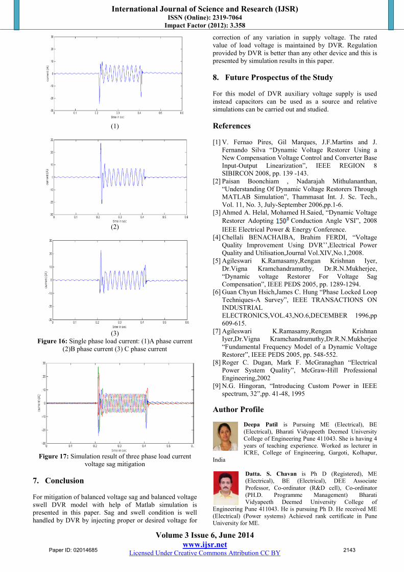
Loadpoint voltage Simulation results show that nominal value of load voltage is maintained by DVR even if sag occurs. In fig 16 and fig 17 load current waveforms for single phase and three phase are presented respectively after mitigation of sag.
Paper ID: 02014685 2142
International Journal of Science and Research (IJSR) ISSN (Online): 2319-7064
Impact Factor (2012): 3.358
Volume 3 Issue 6, June 2014 www.ijsr.net
Licensed Under Creative Commons Attribution CC BY
(1)
(2)
(3)
Figure 16: Single phase load current: (1)A phase current (2)B phase current (3) C phase current
Figure 17: Simulation result of three phase load current
voltage sag mitigation 7. Conclusion For mitigation of balanced voltage sag and balanced voltage swell DVR model with help of Matlab simulation is presented in this paper. Sag and swell condition is well handled by DVR by injecting proper or desired voltage for
correction of any variation in supply voltage. The rated value of load voltage is maintained by DVR. Regulation provided by DVR is better than any other device and this is presented by simulation results in this paper. 8. Future Prospectus of the Study For this model of DVR auxiliary voltage supply is used instead capacitors can be used as a source and relative simulations can be carried out and studied. References [1] V. Fernao Pires, Gil Marques, J.F.Martins and J.
Fernando Silva “Dynamic Voltage Restorer Using a New Compensation Voltage Control and Converter Base Input-Output Linearization”, IEEE REGION 8 SIBIRCON 2008, pp. 139 -143.
[2] Paisan Boonchiam , Nadarajah Mithulananthan, “Understanding Of Dynamic Voltage Restorers Through MATLAB Simulation”, Thammasat Int. J. Sc. Tech., Vol. 11, No. 3, July-September 2006,pp.1-6.
[3] Ahmed A. Helal, Mohamed H.Saied, “Dynamic Voltage Restorer Adopting Conduction Angle VSI”, 2008 IEEE Electrical Power & Energy Conference.
[4] Chellali BENACHAIBA, Brahim FERDI, “Voltage Quality Improvement Using DVR’’,Electrical Power Quality and Utilisation,Journal Vol.XIV,No.1,2008.
[5] Agileswari K.Ramasamy,Rengan Krishnan Iyer, Dr.Vigna Kramchandramuthy, Dr.R.N.Mukherjee, “Dynamic voltage Restorer For Voltage Sag Compensation”, IEEE PEDS 2005, pp. 1289-1294.
[6] Guan Chyun Hsich,James C. Hung “Phase Locked Loop Techniques-A Survey”, IEEE TRANSACTIONS ON INDUSTRIAL ELECTRONICS,VOL.43,NO.6,DECEMBER 1996,pp 609-615.
[7] Agileswari K.Ramasamy,Rengan Krishnan Iyer,Dr.Vigna Kramchandramuthy,Dr.R.N.Mukherjee “Fundamental Frequency Model of a Dynamic Voltage Restorer”, IEEE PEDS 2005, pp. 548-552.
[8] Roger C. Dugan, Mark F. McGranaghan “Electrical Power System Quality”, McGraw-Hill Professional Engineering,2002
[9] N.G. Hingoran, “Introducing Custom Power in IEEE spectrum, 32”,pp. 41-48, 1995
Author Profile
Deepa Patil is Pursuing ME (Electrical), BE (Electrical), Bharati Vidyapeeth Deemed University College of Engineering Pune 411043. She is having 4 years of teaching experience. Worked as lecturer in ICRE, College of Engineering, Gargoti, Kolhapur,
India
Datta. S. Chavan is Ph D (Registered), ME (Electrical), BE (Electrical), DEE Associate Professor, Co-ordinator (R&D cell), Co-ordinator (PH.D. Programme Management) Bharati Vidyapeeth Deemed University College of
Engineering Pune 411043. He is pursuing Ph D. He received ME (Electrical) (Power systems) Achieved rank certificate in Pune University for ME.
Paper ID: 02014685 2143