Embed Size (px)
Citation preview

Art Witulski, Ken Galloway, Scooter Ball, Josh Caldwell, Robert JohnsonRon Schrimpf, Robert Reed, Mike Alles, and John Hutson
Institute for Space and Defense ElectronicsVanderbilt University
Biju Jacob, Ljubisa Stevanovic, Edmund Hindle, Emily Potter General Electric Research and GE Aviation
This project supported by NASA grant 80NSSC 21K0766.
NASA Electrical Parts and Packaging (NEPP) Electronics Technology Workshop
06/15/21
Modeling, Testing, and Simulation of Heavy-Ion Basic Mechanisms in Silicon
Carbide Power Devices
2
VanderbiltEngineeringDefinition of Acronyms
1D-One DimensionalBV-Breakdown Voltage of a material“Epi”-Abbreviation of “Epitaxial”FIT-Failures in TimeGE-General Electric CorporationJBS-Junction-Barrier Schottky DiodeLuSTR-Lunar Surface Technology Research SEB-Single Event BurnoutSEM-Scannng Electron MicroscopeSiC-Silicon CarbideTCAD-Technology Computer-Aided Design SoftwareVU-Vanderbilt UniversityWBG-Wide Bandgap semiconductor material

3
VanderbiltEngineering
NASA ARTEMIS Lunar Program
NASA’s Lunar Exploration Program Overview Sept.2020

4
VanderbiltEngineeringNASA Lunar Surface Technology Research (LuSTR)
LuSTR projects for 2021-2023:
Innovative ways to identify and access resources on the moon• Thermal mining to access and trap water vapor (UTEP)• Rover-mounted drill for water (WUSL)• Heated cone percussive penetrometer for soil/regolith study (MTU)
Next-generation energy storage and power distribution technologies• Wireless transfer feasibility studies for remote power transfer (UCSB)• Silicon carbide power components for lunar surface applications (VU)• Flexible energy distribution between multiple power grids (OSU)
https://www.nasa.gov/directorates/spacetech/lustr/US_Universities_to_Develop_Lunar_Tech_for_NASA

5
VanderbiltEngineeringWide Bandgap Power Devices Electrical Performance
.Choudhury, et al, Semiconductor Science and Technology, 2013.
Same Ron: WBG > 1 decade higher BV-Well suited to high voltage applicationsSame BV: WBT > 2 decades lower Ron-Much more efficient than silicon devices

6
VanderbiltEngineering
Comparative Structure of SiC and SI Power Devices
• SiC Critical field ~8x of Si
• Depletion width much smaller for same breakdown voltage
• Smaller depletion region leads to lower on-resistance
• Higher doping in n- “drift” region in SiC devices than Si
• High fields contribute to more severe single event effects in SiC than in Si
x (microns)
Ele
ctri
c Fi
eld
(M
V/c
m)
Wn-SiC Wn-Si
Normal Electrical Bias: Area under field curve is junction voltage
SiC
Si
𝜙 = −$!!
!"𝐸 𝑥 𝑑𝑥
SiC Epi Si Epi
x
7
VanderbiltEngineering
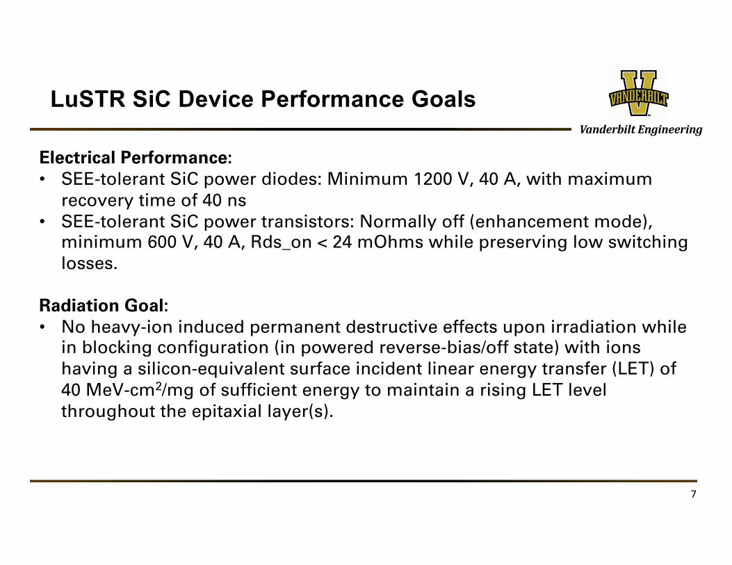
Electrical Performance: • SEE-tolerant SiC power diodes: Minimum 1200 V, 40 A, with maximum
recovery time of 40 ns• SEE-tolerant SiC power transistors: Normally off (enhancement mode),
minimum 600 V, 40 A, Rds_on < 24 mOhms while preserving low switching losses.
Radiation Goal: • No heavy-ion induced permanent destructive effects upon irradiation while
in blocking configuration (in powered reverse-bias/off state) with ions having a silicon-equivalent surface incident linear energy transfer (LET) of 40 MeV-cm2/mg of sufficient energy to maintain a rising LET level throughout the epitaxial layer(s).
LuSTR SiC Device Performance Goals
8
VanderbiltEngineering
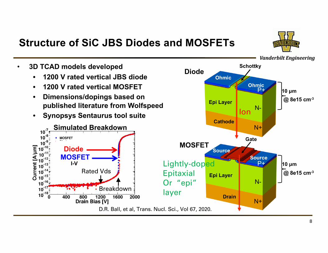
Structure of SiC JBS Diodes and MOSFETs
N+
N-
P+
N+
N-
P+
• 3D TCAD models developed• 1200 V rated vertical JBS diode• 1200 V rated vertical MOSFET• Dimensions/dopings based on
published literature from Wolfspeed• Synopsys Sentaurus tool suite
Simulated Breakdown
Diode
MOSFETMOSFETDiode
I-V
@ 8e15 cm-3
@ 8e15 cm-3
D.R. Ball, et al, Trans. Nucl. Sci., Vol 67, 2020.
Lightly-doped Epitaxial Or “epi” layer
Ion
Rated Vds
Breakdown

9
VanderbiltEngineering
SiC Power MOSFET and Diode SEB and Degradation Thresholds
Rated VoltageMOSFET and Diode SEB
threshold
MOSFET and Diode degradation threshold
1200 V SiC Power MOSFET and Diode show the same SEB and degradation thresholds
SEB Region
Leakage Region
No Damage
All experimentally measured points on 1200 V SiC Devices
D.R. Ball, et al, Trans. Nucl. Sci., Vol 67, 2020.

10
VanderbiltEngineering
• Happens fast – on the order of picoseconds vs. device natural response time of nanoseconds
• Indirectly observed via• Electrical measurements (leakage or short
circuit)• Physical imaging in failure analysis (SEM, etc.)
• LuSTR Task for Caldwell failure analysis Lab at VU
Single Event Physical Damage and Failure Analysis
Kuboyama, et. al, RADECS 2018 Casey, et. al, IEEE TNS Jan. 2018
11
VanderbiltEngineering
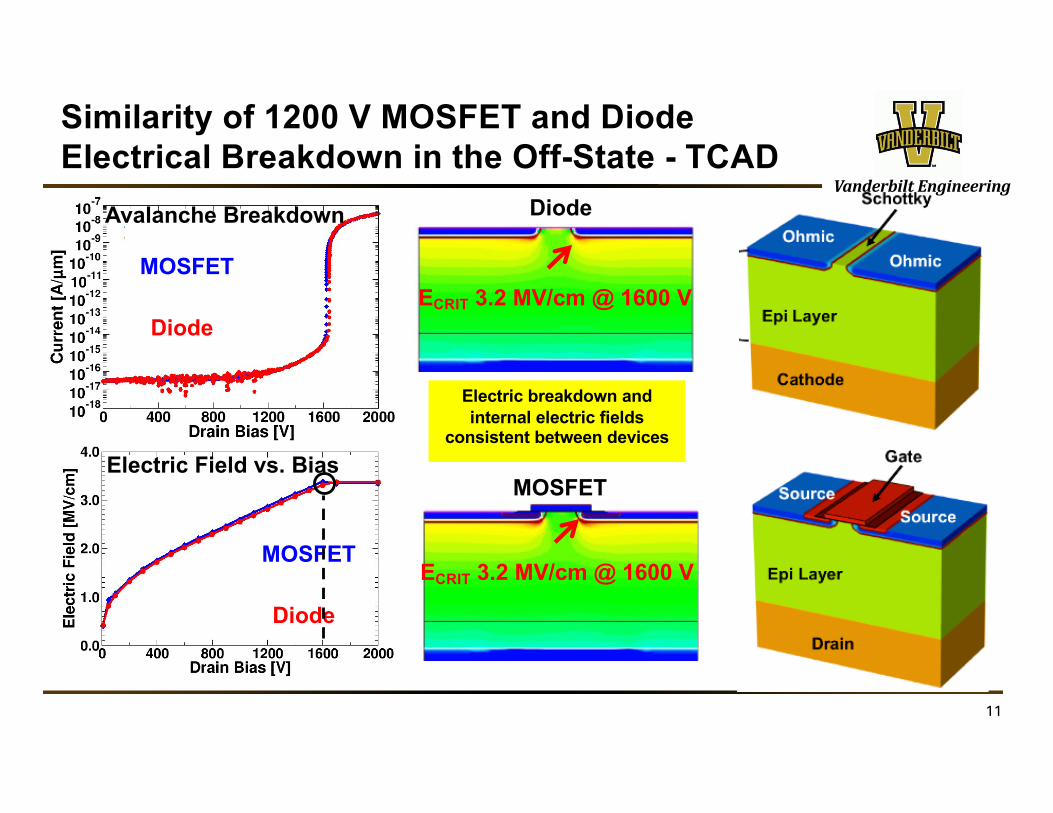
Similarity of 1200 V MOSFET and Diode Electrical Breakdown in the Off-State - TCAD
Electric breakdown and internal electric fields
consistent between devices
Diode
MOSFET
MOSFET
Diode
MOSFET
Diode
Electric Field vs. Bias
ECRIT 3.2 MV/cm @ 1600 V
ECRIT 3.2 MV/cm @ 1600 V
Avalanche Breakdown

12
VanderbiltEngineering
Ion-Induced Re-Distribution of Electric Field During Strike - TCAD
ECRIT
Ion strike at 500 V drain/cathode bias results in…• Short circuit from high carrier density• Re-distribution of bias and electric field• Local field exceeding electrical
breakdown field (3.2 MV/cm which occurs at 1600 V DC )
1D Cutline of Electric Field
Pre-Strike
Post-Strike
Epi/Drain interface
Epi-DrainInterface

13
VanderbiltEngineering
Impact of Voltage Rating and Epitaxial Depth on SEB in SiC
Ion-Induced SEB Terrestrial Neutron-Induced SEB
Data show increased SEB tolerance for thicker, more lightly-doped epitaxial regions
D.R. Ball, et al, IEEE TNS 2021 Early Access on IEEE Xplore
Ion Data from Lauenstein 2017Neutron Data from Lichtenwalner 2018, Wolfspeed Devices
14
VanderbiltEngineering
VU and GE LuSTR Project: Silicon Carbide Power Components for NASA Lunar Surface Applications
TEAM MEMBERS AT VANDERBILT UNIVERSITYo Prof. Arthur F. Witulski, Dr. Dennis R. Ball, Professor Ronald D. Schrimpf, Dr. Andrew Sternberg, Professor
Kenneth F. Galloway, Professor Robert Reed, Professor Michael Alles, and Professor John HutsonTEAM MEMBERS AT GE RESEARCH AND GE AVIATIONo Dr. Biju Jacob, Dr. Ljubisa Stevanovic, Mr. Edmund Hindle, Ms. Emily Potter
APPROACHo Vanderbilt conducts SEE tests on existing GE 3300 V parts to establish baseline performanceo Vanderbilt analyses test results and does TCAD simulation to make recommendations to GE for
hardened devices. o GE designs 3300 V devices that will meet both the SEE-tolerance requirement and electrical
specifications for a candidate diode and transistor.o GE fabricates, tests, packages new MOSFET and diode with hardening strategy (~ 1 year)o In parallel, Vanderbilt continues testing, simulation, materials analysis of existing deviceso Vanderbilt tests new devices to verify success in meeting program requirements.

15
VanderbiltEngineering
Timeline for the LuSTR SiC Project
A R&D/Testing Specific Aims
Months 1 2 3 4 5 6 7 8 9 10 11 12 13 14 15 16 17 18 19 20 21 22 23 241 GE Delivery of Existing Devices to VU
2 VU Preparation for first ion test
3 TCAD Model of SiC Diodes and MOSFETs
4 1st heavy-ion test of GE devices at TAMU
5 GE and VU spec., order wafer
6 VU failure analysis on pristine and post-rad devices
7 VU electrical testing in-situ of pre- and post-rad devices
8 GE mask design
9 GE fabricates RH diode and MOSFET in parallel
10 GE tests, packages, and ships new RH Devices
11 Vanderbilt conducts second heavy-ion test
Objectives 2021
Q1 Q2 Q1
Other tasks Fabrication
2023
Q4Q3
2022
Q2 Q3 Q4 Q1 Q2 Q3 Q4
Major Tasks for LuSTR Project

16
VanderbiltEngineering
Summary for VU-GE LuSTR Program on SiC
• Rad-Hard, high voltage, high current power devices required for lunar exploration
• Silicon carbide naturally suited to these applications (electric vehicles on earth)
• 1200 V SiC devices show vulnerability to SEB at ~40% rated voltage
• VU-GE LuSTR program aims to use 3300 V devices to push SiCSEB boundary to significantly higher voltage, without losing electrical advantages
• Tests on hardened 3300 V devices will take place in Spring 2023


![RBUU Simulation of Heavy-Ion Collisions for RAON · RBUU Simulation of Heavy-Ion Collisions for RAON Lee, ... 30.3 52.1 9. 2015 ECT*-APCTP ... [fm/c] 36 40 44 48 52 56 60 T](https://img.dokumen.tips/doc/110x75/5b2a30187f8b9ad6458bac10/rbuu-simulation-of-heavy-ion-collisions-for-rbuu-simulation-of-heavy-ion-collisions.jpg)