Embed Size (px)
Citation preview

- 1 -
Modeling of Die Surface Features onIntegrated Circuits to Improve Device
Reliability
by
John Sauber
Digital Equipment Corporation
77 Reed Road
Hudson, Massachusetts 01749
Abstract: When semiconductor devices are encapsulatedin plastic, the glass-like dielectric and passivation layers onthe surface of the die are subjected to very high stressesfrom the shrinkage of the molding compound. This paperreviews the modeling approach used to simulate very smallfeatures (~0.1 µm) inside of a relatively large (~28000 µm) package, with the goal of optimizing the design to eliminatedevice failure caused by cracking of the dielectric andpassivation layers.

- 2 -
INTRODUCTION
A complex stress state exists inside of a semiconductor device caused by the series of processsteps which is used in its fabrication. A large single crystal of silicon is sliced into "wafers"which are typically 6" to 8" in diameter, but only 0.011" to 0.024" thick. Using vapor deposi-tion and photo-imageable masking technology, up to four alternating layers of aluminum andglass-like PETEOS dielectric (Plasma Enhanced TetraEthylOrthoSilicate, commonly called"oxide") are applied to the surface of the wafer. Since these layers are deposited at high tem-peratures (340°C to 390°C) and since the aluminum and the oxide have very different thermalexpansion coefficients (23 ppm/°C and 0.5 ppm/°C respectively) a great deal of intrinsic stressis generated when the devices are cooled to room temperature.
After depositing a final "passivation layer" of silicon nitride (Si3N4, commonly called "nitride")to protect the circuits from moisture, the wafer is sawed apart to singulate the individual dies. The dies are tested electrically, and then installed into a package which is typically made ofeither ceramic (for high power/high cost devices) or plastic (for low power/low cost devices). For plastic packaging, the die is mounted on the "die pad" portion of a copper leadframe usingan epoxy adhesive, and then connected electrically to the "bond fingers" in the leadframe usingfine (0.001" diameter) gold bond wires as shown in Figure 1. The leadframe/die assembly isthen encapsulated in a silica filled, Novolac epoxy molding compound using a transfer moldingprocess.
Figure 1 -- Silicon die mounted on leadframe prior to encapsulation
bondfingers
bondwires
surface of die
die pad

- 3 -
STATEMENT OF PROBLEM
As previously mentioned, the die fabrication process creates high intrinsic stresses in the dielec-tric layers, the aluminum lines and the passivation layer on the surface of the die. When the dieis encapsulated, additional stresses are generated by the expansion differential between the dieand molding compound as the device cools to room temperature. To further complicate the is-sue, the adhesive bond between the molding compound sometimes will fail (delaminate) whichcan concentrate the forces and stresses on the various features on the die’s surface. If thestresses are high enough, it is possible for the the passivation layer and/or the dielectric layersto crack. Once this has occurred, moisture can penetrate into the aluminum lines which cancause corrosion which can lead to failure. Focused Ion Beam (FIB) technology was used to ex-pose the inside of the die surface revealing the cracked dielectric and passivation layers shownin Figure 2.
Figure 2 -- Cracks in the dielectric and passivation layers caused by stressesfrom the molding compound
ANALYSIS
Models
The difficulty with modeling this structure is that the features which are of interest are verysmall, requiring elements which are only ~0.1 µm on a side. To put this in perspective, a hu-man hair is typically about 75 µm in diameter. The device itself is a relatively large 28,000 µmacross, and since interactions between the various components in the package have a direct ef-fect on the stresses on the die surface, the whole package must be modeled. While it is possibleto solve this problem using submodeling [1,2], the Mesh Paver utility in PATRAN1 makes itfairly simple to model the entire structure. Figures 3, 4, and 5 show how the package is mod-eled.
moldingcompound
passivation
aluminumlines
dielectric
dielectric
1PATRAN is a registered trademark of the MacNeal-Schwendler Corporation

- 4 -
Figure 3 -- Model of a diagonal cross section of the package (partial)
Figure 4 -- Close-up of corner of die
Figure 5 -- Extreme close-up of die surface with lines, dielectric and passivation
die
die attach
dielectric andpassivation
die pad
moldingcompound
dielectric andpassivationlayers
die
moldingcompound
passivation
aluminumlines
dielectric
moldingcompound
3µm
- 5 -
Elements
MSC/ABAQUS1 4 node axisymmetric elements (CAX4) were used. It was necessary to use a2-D approximation because any 3-D model fine enough to include the sub-micron featureswould have required such a large amount of solution time that our funding would have expiredbefore any results were obtained. Since this is actually simulating a disk shaped die instead of asquare die, a study was conducted to determine the amount of error caused by the approxima-tion. A 3-D model of the device was built using elements which were .005" (127 µm) on a side. Two axisymmetric models were built of the same device, one simulating a section from the cen-ter to the edge of the package, the other simulating a section from the center to the corner of thepackage. The amount of error in the Von Mises stress in the passivation layer for the twoaxisymmetric models compared to the 3-D model is shown in Figure 6 as a function of location(normalized distance from the center of the die).
Figure 6 -- Accuracy of axisymmetric models vs. location on die surface
Not surprisingly, both of the axisymmetric models were fairly accurate near the center of thedie. The center-to-edge model was accurate across most of the die surface, and was only off by26% at the edge of the die. The center-to-corner model was off by considerably more, produc-ing an error of 67% in the very corner of the die. Examining the source of the error showedthat the center-to-corner model was not taking into account the "squeezing" effect that themolding compound exerts on the corner of the die. Fortunately, the goals of the project onlyrequired that we evaluate the relative merits of various design options. Since the features to be
0 10 20 30 40 50 60 70 80 90 100% of Distance from Center to Edge
0
10
20
30
40
50
60
70
% o
f Erro
r in
Axisy
mm
etric
Mod
el vs
3D
From center to corner (diagonally)
From center to edge (along centerline)
1MSC/ABAQUS is a trademark of the MacNeal-Schwindler Corporation

- 6 -
evaluated were all located on the same small section of the die surface, the results producedwould be acceptable for comparing the relative impact of design changes to those features.
The use of the "economical" axisymmetric elements proved to be quite important. Even thoughtypical models had anywhere from 6,000 and 11,000 elements, our Digital AlphaStation1 6005/266 workstation was able to solve them in only 1 or 2 minutes per iteration. However, thecontact surfaces needed to simulate interfacial delamination required dozens of iterations perload case to converge, and many load cases were needed to quantify the effects of the manydesign variables, so hundreds of iterations had to be solved to complete the project. This wouldnot have been possible if a 3-D modeling approach had been used.
Material Properties
The SRC/CINDAS Microelectronics Packaging Materials Database [3] was used to find theproperties of the various materials. The properties of the aluminum, dielectric and passivationwere derived from testing of thin film materials which were deposited using processes that wereidentical to those used in actual production. This is an important detail since thin film proper-ties are often quite different from bulk properties.
Accuracy
The ability of the model to accurately predict the stresses in the dielectric and passivation wasverified by examining the stresses in areas of the die surface which do not contain any metallines. The CINDAS database includes data on nitride or oxide film stress (F.S.) calculated fromwafer curvature measurements by using the following equation:
Where E is the Young’s modulus for the Si substrate, N is its poisson’s ratio, D is the thicknessof substrate, t is the film thickness, and R is the net radius of curvature. Digital also routinelyconducts these tests as a method for process control, and obtains the same results that CINDASdoes. Models built of an oxide-only or nitride-only film over silicon provide extremely goodcorrelation with oxide stresses being within 1% and nitride stresses being within 10% of thepublished values. While this does not insure that every result for every metal line structure iscorrect, it does provide a good "sanity check" on the material properties and loading conditions.
F.S. = (E * D**2)/6*(1-N)*R*t (1)
1AlphaStation is a registered trademark of Digital Equipment Corporation

- 7 -
Modeling Procedure
In order to simulate the assembly procedure, the analysis must be done in three steps:
1. The entire finished assembly is modeled, but the modulus of the molding compound is set toa very low number so that it is essentially "invisible". This model is solved for coolingfrom the dielectric/passivation deposition temperature (390°C) to the molding temperature (150°C).
2. The same model is solved for cooling from the molding temperature (150°C) to room tem-perature, only this time the actual molding compound properties are used.
3. Since these are linear materials, superposition can be used to combine the two load cases. Using the the PATRAN post-processor, the component stresses are combined and then theprincipal stresses are recalculated.
Figures 7, 8 and 9 show the major principal stresses and deformed shape for each of these steps.
Figure 7 -- Cooling from 390°C to 150°C -- No Molding Compound
239.4
214.6
189.9
165.1
140.3
115.6
90.80
66.03
41.27
16.50
-8.267
-33.03
-57.80
-82.57
-107.3
-132.1

- 8 -
Figure 8 -- Cooling from 150°C to 20°C -- With Molding Compound
Figure 9 -- Cooling from 390°C to 20°C -- Combined Load
140.4
126.6
112.8
99.04
85.25
71.47
57.68
43.89
30.11
16.32
2.533
-11.25
-25.04
-38.83
-52.61
-66.40
377.5
340.1
302.7
265.3
227.9
190.5
153.1
115.7
78.25
40.84
3.433
-33.97
-71.38
-108.8
-146.2
-183.6

- 9 -
An examination of the principal stresses in the dielectric and passivation layer near the alumi-num lines shows that the intermediate and minor principal stresses are mostly compressive,while the major principal stress is tensile. As is the case with many glass-like materials, thestrength of the oxide and the nitride is much higher in compression than it is in tension, so, fail-ure is most likely to be caused by the major principal stress. Figure 10 shows the directions ofthe principal stresses near the aluminum lines. The view is rotated slightly so that the out ofplane stresses can be seen. The stresses in the line and the molding compound are not shown.
Figure 10 -- Directions of the principal stresses in the dielectric and passivationnear an aluminum line
Optimizing Layer Thicknesses and Process Parameters
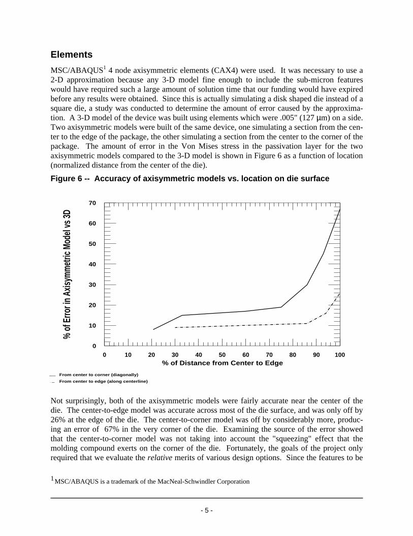
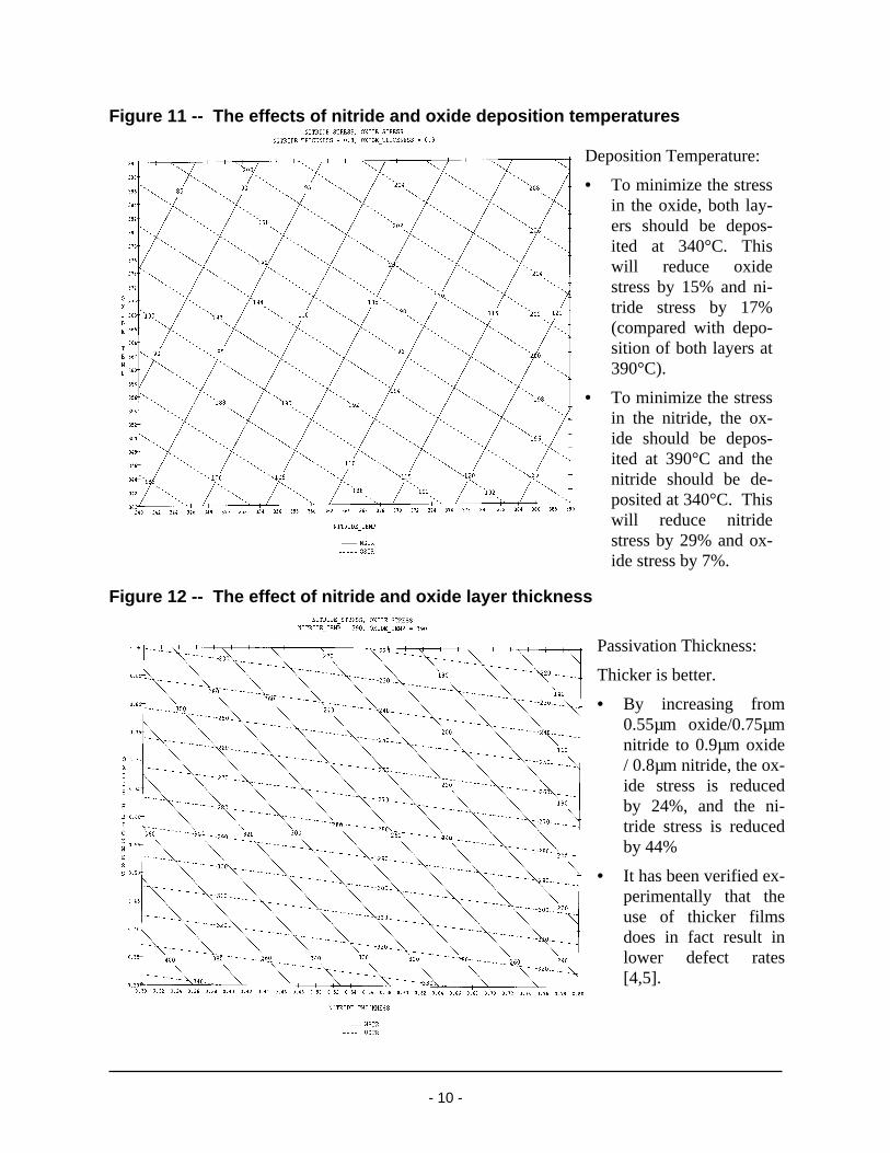
The analysis method was used to optimize the thicknesses and deposition temperatures of thepassivation and top dielectric layers, and to select the best material choices for the moldingcompound and die attach adhesive. Response surface modeling using the RS1/Discover1 soft-ware was used to interpolate between the variables. This approach minimizes the number ofload cases which must be solved to understand a problem which is affected by several variables. Figure 11 shows the impact of deposition temperature on nitride and oxide stresses, while Fig-ure 12 shows the effects of layer thickness.
aluminum line is inthis area
(stresses not shown)
molding compound isin this area
(stresses not shown)
passivationlayer
top leveldielectric
layer
1RS1/Discover is a registered trademark of Bolt Beranek and Newman Inc.
- 10 -
Figure 11 -- The effects of nitride and oxide deposition temperatures
Figure 12 -- The effect of nitride and oxide layer thickness
Deposition Temperature:
• To minimize the stressin the oxide, both lay-ers should be depos-ited at 340°C. Thiswill reduce oxidestress by 15% and ni-tride stress by 17%(compared with depo-sition of both layers at390°C).
• To minimize the stressin the nitride, the ox-ide should be depos-ited at 390°C and thenitride should be de-posited at 340°C. Thiswill reduce nitridestress by 29% and ox-ide stress by 7%.
Passivation Thickness:
Thicker is better.
• By increasing from0.55µm oxide/0.75µmnitride to 0.9µm oxide/ 0.8µm nitride, the ox-ide stress is reducedby 24%, and the ni-tride stress is reducedby 44%
• It has been verified ex-perimentally that theuse of thicker films does in fact result inlower defect rates[4,5].

- 11 -
The Effects of Molding Compound Properties and Delamination
Scanning acoustic micrography (C-SCAN) results have shown that in some cases a loss of ad-hesion (delamination) occurs between the molding compound and the passivation layer. Tosimulate this condition, MSC/ABAQUS contact surfaces were used to allow sliding contact atthe interface. Results were produced for both the standard Plastic Quad Flat Pack (PQFP) andthe thermally enhanced PQFP which contains a large copper heatspreader underneath the diepad. This study also included an examination of the effects of molding compound CTE andmodulus, and the die attach adhesive modulus since these are known to have an effect on thedie surface stresses [2,6,7]. Figure 13 shows a typical deformed shape for the structure and theresulting stress concentration in the passivation layer. The location of the peak tensile stressesagrees with the failure mode observed by Lesk, et al [8] in cases where molding compound /passivation delamination has occurred. Figures 14 and 15 (on the following page) show re-sponse surface graphs of the results. Points on the graph show the various grades of moldingcompounds (i.e., "A", "B" & "C") which are available.
Figure 13 -- Passivation stresses and deformed shape when delamination of thepassivation / molding compound interface occurs

- 12 -
Figure 14 -- Effect of molding compound CTE and elastic modulus on nitridestress when a low modulus die attach adhesive is used
Figure 15 -- Effect of molding compound CTE and elastic modulus on nitridestress when a high modulus die attach adhesive is used
AA
B
CB
C
C
A B
B
A
C
BA C
A
B
C

- 13 -
Several conclusions can be drawn from these studies:
• Delamination has a huge effect resulting in a factor of 12 to 20 increase in passivation layerstresses. All other considerations are secondary compared to the need to eliminate or con-trol the effects of delamination. Test results [9] have shown that delamination is one of themain causes of electrical failure. Delamination has also been shown to cause up to a 10 foldincrease in the molding compound stress intensity factor which can result in cracking of theentire package [10].
• Reducing molding compound CTE from 20 to 10 ppm/°C reduces the nitride stress by any-where from 32% to 56%
• Reducing molding compound modulus from 20 to 10 GPa reduces the nitride stress by any-where from 22% to 40%
• The product of molding compound (CTE) x (modulus) is an effective indicator of the rela-tive "goodness" of a molding compound. This relationship (which is sometimes referred toas the resin parameter) has been observed in test results from other researchers [11].
• Reducing die attach modulus from 8 to 0.4 GPa reduces the nitride stress by:- Anywhere from 8% to 11% for PQFPs- Anywhere from 0% to 6% for EPQFPs
• Using a PQFP instead of an EPQFP reduces the nitride stress by anywhere from 6% to 28%
• Molding compound choices:- Using molding compound C instead of A reduces the nitride stress by 7%- Using molding compound A instead of B reduces the nitride stress by 5%- Using molding compound C instead of B reduces the nitride stress by 12%
Several methods for controlling the effects of delamination have been modeled, built and tested,but since the patent process for these designs has not yet been completed they are consideredproprietary and cannot be described in this paper.
SUMMARY
An analysis method was developed for calculating the stresses which occur in the top level di-electric and passivation layers on the surface of a semiconductor die. The assembly processwas simulated by solving load cases for the steps before and after encapsulation, and then com-bining the results in the post-processor. A series of models were solved to quantify the amountof error at various locations on the die caused by using an axisymmetric approximation of thestructure. The method was used to identify the optimum layer thicknesses and deposition tem-peratures for minimizing the dielectric and passivation layer stresses. Models were built withsliding surfaces to simulate delamination of the molding compound / passivation layer inter-face. The differences between standard PQFP devices and thermally Enhanced PQFPs wereevaluated. Finally, a series of models were solved to determine the effects of molding com-pound and die attach adhesive material properties, and to select the best commercially availablematerials.

- 14 -
ACKNOWLEDGMENTS
This work would not have been possible without the hard work and support shown by manyindividuals. In particular the author would like to acknowledge the contributions of AntonioBerti, Ahsan Enver, Wendy Fowler, Jim Gardner, Terri Giversen, Jaime Ide, Larisa Kisselgof,John Kowaleski, Lidia Lee, Jeff Maggard, Tom McCoy, Wade McFaddin, Hon Nguyen andBrian Walker.
REFERENCES
1. Michael, M.M., "Stress analysis for large die plastic packages", Proc. of the National Elec-tronic Packaging and Production Conf., NEPCON East, 1991 pp. 435-445.
2. Pendse, R., and Demmin, J., "Test structures and finite element models for chip stress andplastic package reliability", Proc. International Conf. on Microelectronic Test Structures",1990, pp. 155-160.
3. Center for Information and Numerical Data Analysis and Synthesis (CINDAS), Micro-electronics Packaging Materials Database, Purdue University, developed under the sponsor-ship of the Semiconductor Research Corporation (SRC), Update #14, Sept. 1995.
4. Kato, H., Sakai, H. and Sugawara, K., "Microdefects in oxide films deposited on featuredsurfaces of VLSI substrates by thermal CVD of TEOS and O2", J. of Electrochem. Soc.,Vol. 141, No. 11, Nov. 1994, pp. 3154-3157.
5. Wu, T., and O’Brien, K., "Comparison of passivation films: the effect of thermal cyclesand comparison of phosphorous doped oxide films", J. of Vacuum Science Technology, B11(6), Nov./Dec. 1993, pp. 2090-2095.
6. Foehringer, R., Golwalkar, S., Eskildsen, S. and Altimari, S., "Thin film cracking in plasticpackages - analysis, model and improvements", Proc. 41st Electronic Components andTechnology Conf., 1991, pp. 759-765.
7. Zelenka, R., "A reliability model for interlayer dielectric cracking during temperature cy-cling", 29th Annual Proc. Reliability Physics, 1991, pp. 30-34.
8. Lesk, I., Thomas, R., Hawkins, G., Remmel, T., and Rugg, J., "Progression of damagecaused by temperature cycling on a large die in a molded plastic package", Proc. 40th Elec-tronic Components and Technology Conf., 1990, pp. 807-812.
9. Doorselaer, K., and Zeeuw, K., "Relationship between delamination and temperature-cycling induced failures in plastic packaged devices", Proc. 40th Electronic Componentsand Technology Conf., 1990, pp. 813-817.
10. Sauber, J., Lee, L., Hsu, S., and Hongsmatip, T., "Fracture properties of molding compound materials for IC plastic packaging", IEEE Transactions on Components, Packaging andManufacturing Technology, Vol 17, No. 4, Dec. 1994, pp. 533-541.
11. Miura, H., Nishimura, A. and Kawai, S., "Structural effect of IC plastic package on residualstress in silicon chips", Proc. 40th Electronic Components and Technology Conf., 1990, pp.316-321.