Embed Size (px)
Citation preview

MEMORYmaster�™User’s Guide
WindowsNT ™�and UNIX ® Environments

Actel Corporation, Sunnyvale, CA 94086© 1999 Actel Corporation. All rights reserved.
Printed in the United States of America
Part Number: 5579017-0
Release: November 1999
No part of this document may be copied or reproduced in any form or by any means without prior written consent of Actel.
Actel makes no warranties with respect to this documentation and disclaims any implied warranties of merchantability or fitness for a particular pur-pose. Information in this document is subject to change without notice.
Actel assumes no responsibility for any errors that may appear in this doc-ument.
This document contains confidential proprietary information that is not to be disclosed to any unauthorized person without prior written consent ofActel Corporation.
TrademarksActel and the Actel logotype are registered trademarks of Actel Corporation.
Adobe and Acrobat Reader are registered trademarks ofAdobe Systems, Inc.
MEMORYmaster is a trademark of Gatefield, Inc.
ASICmaster is a trademark of Gatefield, Inc.
Synopsys is a registered trademark of Synopsys Inc.
Verilog is a registered trademark of Open Verilog International.
UNIX is a registered trademark of X/Open Company Limited.
Windows is a registered trademark and Windows NT is a trademark ofMicrosoft Corporation in the U.S. and other countries.
All other products or brand names mentioned are trademarks or registered trademarks of their respective holders.
ii
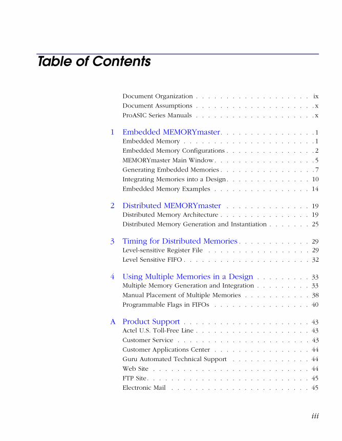
Table of Contents
Document Organization . . . . . . . . . . . . . . . . . . . ix
Document Assumptions . . . . . . . . . . . . . . . . . . . . x
ProASIC Series Manuals . . . . . . . . . . . . . . . . . . . . x
1 Embedded MEMORYmaster. . . . . . . . . . . . . . . . 1Embedded Memory . . . . . . . . . . . . . . . . . . . . . . 1
Embedded Memory Configurations . . . . . . . . . . . . . . . 2
MEMORYmaster Main Window. . . . . . . . . . . . . . . . . 5
Generating Embedded Memories . . . . . . . . . . . . . . . . 7
Integrating Memories into a Design . . . . . . . . . . . . . . 10
Embedded Memory Examples . . . . . . . . . . . . . . . . 14
2 Distributed MEMORYmaster . . . . . . . . . . . . . . 19Distributed Memory Architecture . . . . . . . . . . . . . . . 19
Distributed Memory Generation and Instantiation . . . . . . . 25
3 Timing for Distributed Memories . . . . . . . . . . . . 29Level-sensitive Register File . . . . . . . . . . . . . . . . . 29
Level Sensitive FIFO . . . . . . . . . . . . . . . . . . . . . 32
4 Using Multiple Memories in a Design . . . . . . . . . 33Multiple Memory Generation and Integration . . . . . . . . . 33
Manual Placement of Multiple Memories . . . . . . . . . . . 38
Programmable Flags in FIFOs . . . . . . . . . . . . . . . . 40
A Product Support . . . . . . . . . . . . . . . . . . . . . 43Actel U.S. Toll-Free Line . . . . . . . . . . . . . . . . . . . 43
Customer Service . . . . . . . . . . . . . . . . . . . . . . 43
Customer Applications Center . . . . . . . . . . . . . . . . 44
Guru Automated Technical Support . . . . . . . . . . . . . 44
Web Site . . . . . . . . . . . . . . . . . . . . . . . . . . 44
FTP Site. . . . . . . . . . . . . . . . . . . . . . . . . . . 45
Electronic Mail . . . . . . . . . . . . . . . . . . . . . . . 45
iii

Table of Contents
Worldwide Sales Offices . . . . . . . . . . . . . . . . . . . 46
iv
List of Figures
Embedded Memory and Standard Logic Cells (tiles) . . . . . . . . . 1
MEMORYmaster Main Window . . . . . . . . . . . . . . . . . . 5
MEMORYmaster Window Ports Tab . . . . . . . . . . . . . . . . 6
ASICmaster Toolbar . . . . . . . . . . . . . . . . . . . . . . . . 8
ASICmaster Tools Dialog Box . . . . . . . . . . . . . . . . . . . 8
Working Directory File Browser . . . . . . . . . . . . . . . . . . 9
MEMORYmaster Main Window . . . . . . . . . . . . . . . . . 15
2x2 Register File Schematic . . . . . . . . . . . . . . . . . . . 20
2x2 FIFO Schematic . . . . . . . . . . . . . . . . . . . . . . . 21
Horizontal Memory . . . . . . . . . . . . . . . . . . . . . . . 22
Vertical Memory . . . . . . . . . . . . . . . . . . . . . . . . 23
Design Example . . . . . . . . . . . . . . . . . . . . . . . . 25
Distributed MEMORYmaster User Interface . . . . . . . . . . . . 26
Level-sensitive Mode Timing Diagram . . . . . . . . . . . . . . 29
Edge-triggered Mode Timing Diagram . . . . . . . . . . . . . . 30
Edge-triggered FIFO Timing Diagram . . . . . . . . . . . . . . 32
Sample Design . . . . . . . . . . . . . . . . . . . . . . . . . 33
MEMORYmaster Window Showing a Sample FIFO . . . . . . . . 34
Sample Memory Placement . . . . . . . . . . . . . . . . . . . 37
Sample FIFO Placement . . . . . . . . . . . . . . . . . . . . . 38
v

List of Tables
Embedded Memory Block Configurations . . . . . . . . . . . . . 2
Possible RAM Locations for the A500K Family . . . . . . . . . . 13
Maximum RAM and FIFO Dimensions . . . . . . . . . . . . . . 22
Decoder Sizes . . . . . . . . . . . . . . . . . . . . . . . . . 23
RAM . . . . . . . . . . . . . . . . . . . . . . . . . . . . . . 39
FIFO . . . . . . . . . . . . . . . . . . . . . . . . . . . . . . 40
vii


Introduction
The MEMORYmaster User’s Guide contains information and procedures for using the MEMORYmaster software to create embedded and distributed memories to use in ProASIC devices. This guide also includes information about all the possible configurations of RAMs and FIFOs that MEMORYmaster can generate and includes brief examples of how to instantiate the generated memories into a design. Also, information about timing for distributed memories as well as using multiple memories, in a design is presented.
MEMORYmaster includes two independent tools, Embedded MEMORYmaster, which generates memories using embedded memory blocks, and the Distributed MEMORYmaster, which generates distributed memories using core logic tiles.
Document OrganizationThe MEMORYmaster User’s Guide is divided into the following chapters:
Chapter 1- Embedded MEMORYmaster lists all the possible configurations of embedded RAMs and FIFOs that MEMORYmaster can generate. It also describes using the memory generator and includes two examples for generating a RAM and FIFO.
Chapter 2- Distributed MEMORYmaster describes the architecture of distributed RAMs and FIFOs that are implemented in the logic tiles of ProASIC devices. The command line user interface is also described and an example of generating a distributed RAM is included.
Chapter 3- Timing for Distributed Memories presents the timing parameters for level sensitive, edge-triggered register files and FIFOs.
Appendix 4- Using Multiple Memories in a Design provides an example of a design using one FIFO for receiving and another for sending data. Generation and integration of the FIFOs is also shown. Particular attention is given to their placement in embedded memory blocks of a device.
Appendix A- Product Support provides information about contacting Actel for customer and technical support.
ix
Introduction
Document AssumptionsThe information in this guide is based on the following assumptions:
1. You have installed the ASICmaster software.
2. You are familiar with the principles of digital design.
3. You are familiar with UNIX and Microsoft Windows NT operating systems
ProASIC Series ManualsThe ASICmaster Series software includes printed and on-line manuals. The on-line manuals are in PDF format on the CD-ROM in the “/doc” directory. These manuals are also installed onto your system when you install the ASICmasters software. To view the on-line manuals, you must install Adobe® Acrobat Reader® from the CD-ROM.
ASICmaster Installation and Licensing Guide provides information and procedures for installing and licensing the ASICmaster software.
MEMORYmaster User’s Guide provides information and procedures for generating embedded and distributed memories and instantiating them into a design.
ProASIC Interface Guide provides information and procedures for designing ProASIC devices using Exemplar synthesis, Synopsys synthesis, Verilog simulation, and VHDL simulation environments.
Synopsys Synthesis Methodology Guide for ProASIC Device contains information and procedure for using Synopsys FPGA Compiler to design ProASIC Devices.
ASICmaster User’s Guide provides information about creating designs for ProASIC device. It includes information and procedures for placing and routing designs and information about using timing constraints.
ProASIC Macro Library Guide provides descriptions of library elements for ProASIC devices. Symbols, truth tables, and timing parameters are included for all macros.
x

Introduction
FlashTimer User’s Guide contains information and procedure for using FlashTimer to perform static timing analysis on ProASIC designs.
A Guide to ACTgen Macros provides descriptions of macros that can be generated using the Actel ACTgen Macro Builder software.Including macros that can be generated for ProASIC devices
xi


1Embedded MEMORYmaster
This chapter describes how to use the Embedded MEMORYmaster to generate embedded memories for ProASIC devices, instantiate the memory into the design source code, simulate and synthesize the design, and import the netlist into ASICmaster. It includes a description of ProASIC dedicated memory blocks and all their possible configurations.
Embedded MemoryProASIC devices contain dedicated embedded memory blocks and standard logic cells called tiles. The embedded memory blocks are shown in the upper section of the ASICmaster Viewer, shown in Figure 1-1.
Figure 1-1. Embedded Memory and Standard Logic Cells (tiles)
EmbeddedMemoryBlocks
Core LogicTiles
1
Chapter 1: Embedded MEMORYmaster
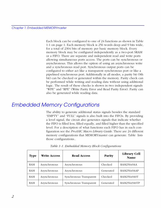
Each block can be configured to one of 24 functions as shown in Table 1-1 on page 1. Each memory block is 256 words deep and 9 bits wide, for a total of 2304 bits of memory per basic memory block. Every memory block may be configured independently as a two-port SRAM or a FIFO. There are separate and independent read and write ports allowing simultaneous ports access. The ports can be synchronous or asynchronous. This allows the option of using an asynchronous write and a synchronous read port. Synchronous output ports can be configured to either act like a transparent synchronous port or like a pipelined synchronous port. Additionally in all modes, a parity bit (9th bit) can be checked or generated within the memory. Parity check can be performed while writing and reading data without using additional logic. The result of these checks is shown in two independent signals “WPE” and “RPE” (Write Parity Error and Read Parity Error). Parity can also be generated while reading data.
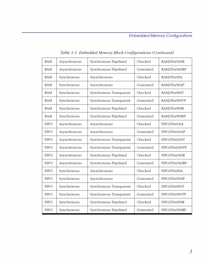
Embedded Memory ConfigurationsThe ability to generate additional status signals besides the standard “EMPTY” and “FULL” signals is also built into the FIFOs. By providing a level signal, the circuit also generates signals that indicate whether the FIFO is filled less, filled equally, and filled higher than the specified level. For a description of what functions each FIFO has in each con-figuration see the ProASIC Macro Library Guide. There are 24 different memory configurations that MEMORYmaster can generate. Table lists those configurations..
Table 1-1. Embedded Memory Block Configurations
Type Write Access Read Access ParityLibrary Cell
Name
RAM Asynchronous Asynchronous Checked RAM256x9AA
RAM Asynchronous Asynchronous Generated RAM256x9AAP
RAM Asynchronous Synchronous Transparent Checked RAM256x9AST
RAM Asynchronous Synchronous Transparent Generated RAM256x9ASTP
2
Embedded Memory Configurations
RAM Asynchronous Synchronous Pipelined Checked RAM256x9ASR
RAM Asynchronous Synchronous Pipelined Generated RAM256x9ASRP
RAM Synchronous Asynchronous Checked RAM256x9SA
RAM Synchronous Asynchronous Generated RAM256x9SAP
RAM Synchronous Synchronous Transparent Checked RAM256x9SST
RAM Synchronous Synchronous Transparent Generated RAM256x9SSTP
RAM Synchronous Synchronous Pipelined Checked RAM256x9SSR
RAM Synchronous Synchronous Pipelined Generated RAM256x9SSRP
FIFO Asynchronous Asynchronous Checked FIFO256x9AA
FIFO Asynchronous Asynchronous Generated FIFO256x9AAP
FIFO Asynchronous Synchronous Transparent Checked FIFO256x9AST
FIFO Asynchronous Synchronous Transparent Generated FIFO256x9ASTP
FIFO Asynchronous Synchronous Pipelined Checked FIFO256x9ASR
FIFO Asynchronous Synchronous Pipelined Generated FIFO256x9ASRP
FIFO Synchronous Asynchronous Checked FIFO256x9SA
FIFO Synchronous Asynchronous Generated FIFO256x9SAP
FIFO Synchronous Synchronous Transparent Checked FIFO256x9SST
FIFO Synchronous Synchronous Transparent Generated FIFO256x9SSTP
FIFO Synchronous Synchronous Pipelined Checked FIFO256x9SSR
FIFO Synchronous Synchronous Pipelined Generated FIFO256x9SSRP
Table 1-1. Embedded Memory Block Configurations (Continued)
3

Chapter 1: Embedded MEMORYmaster
NamingConventions
The HDL models for each of the 24 possible configurations are included in the ProASIC simulation and synthesis library. The function and timing of each model is described in detail in the ProASIC Macro Library Guide and the ProASIC 500K Family Datasheet.The modules are named according to the following convention:
<MEM-TYPE><256x9><WRITE-ACCESS><READ-ACCESS><PARITY>
<MEM-TYPE> := RAM or FIFO;<WRITE-ACCESS> := A, S;
A := asynchronous;S := synchronous;
<READ-ACCESS> := A, ST, SR;A := asynchronous;ST := synchronous transparent;SR := synchronous registered;
<PARITY> := P or nothing;P := parity will be generated;nothing := parity will be checked;
For example, the name of a FIFO with an asynchronous write and a synchronous transparent read mode with parity check is “FIFO256x9AST.” Or a synchronous registered RAM with parity bit generation would be named “RAM256x9SSRP.”
4

MEMORYmaster Main Window
MEMORYmaster Main WindowWhen you invoke MEMORYmaster, the main window is displayed, as shown in Figure 1-2. From this window, the format of embedded memory, the target ProASIC family, and the configuration of the memory are selected. MEMORYmaster is not part specific. You must ensure that the target device has sufficient memory resources to accommodate the memory blocks. For example, the A500K130 has 20 basic 256x9 bit memory resources available. If a 512x32 bit FIFO is created using MEMORYmaster, then every instance of that FIFO in the design will use eight of the available memory resources.
Figure 1-2. MEMORYmaster Main Window
5

Chapter 1: Embedded MEMORYmaster
Ports Tab The Ports tab, shown in Figure 1-3, allows the specification of names for ports used in the netlist. Default names are automatically provided. Only those signal fields relevant to the selected memory type are active.
Figure 1-3. MEMORYmaster Window Ports Tab
The bus switch next to the Data In and Data Out fields allows you to specify whether to treat these signals as bus or single bit (flat) ports. You can also select whether control signals are active high or active low.
ConfigurationTab
The Configuration tab in the MEMORYmaster main window, as shown in Figure 1-2 on page 5, allows you to name the memory block currently being created and to select its parameters. MEMORYmaster can create RAMs and FIFOs of different widths, depths, access modes, and parity, etc. One option available only for RAMs is to write enable an individual byte that is wider than 8 bits. This is accomplished by checking the Use Byte Control checkbox to enable the appropriate write flag. One option only available for FIFOs is the ability to set the FIFO trigger level signal as either static or dynamic. This level signal is
6

Generating Embedded Memories
used to set programmable flags. The value of this signal determines the occurrence of the “EQTH” and “GEQTH” signals.
The Resource Usage section is updated as changes are made to reflect the number of memory and logic tiles that the memory block requires in its implementation. The basic embedded 256x9 bit RAM or FIFO requires no logic core tiles. Logic core tiles are required for implementing embedded memories that are wider and/or deeper than 256x9 bit. The use of core resources is also dependent on the user’s choice to generate a memory optimized for speed or area. Figure 1-2 on page 5 shows a memory that is optimized for area. Optimizing for area required eight memory blocks and 53 core tiles. If it is optimized for speed the FIFO would be mapped to 8 memory blocks and 162 core tiles.
Generating Embedded MemoriesMEMORYmaster generates memories in Verilog ® , VHDL or EDIF format. One memory block or multiple blocks can be generated, and the blocks may reside in one or more netlist files. A constraints file, containing placement directives for each memory, is also generated. The constraint data for each block may reside in one or more constraint files. Use the following procedure to generate an embedded memory with Embedded MEMORYmaster.
1. Invoke Embedded MEMORYmaster.
PC
Select ASICmaster from the ASICmaster menu under programs in the Start menu.
UNIX
Type the following command at the prompt:
asicmaster
The ASICmaster Toolbar is displayed as shown in Figure 1-4 on page 8.
7

Chapter 1: Embedded MEMORYmaster
Figure 1-4. ASICmaster Toolbar
2. Click the Tools button. The ASICmaster Tools dialog box is displayed as shown in Figure 1-5 on page 8.
Figure 1-5. ASICmaster Tools Dialog Box
3. Click the Build Embedded Memories button. The Working Directory File Browser is displayed as shown in Figure 1-6 on page 9.
4. (PC Only) You must first set a working directory for your design and click the Select button as shown in Figure 1-6 on page 9. The MEMORYmaster main window is displayed as shown in Figure 1-2 on page 5.
8

Generating Embedded Memories
Figure 1-6. Working Directory File Browser
5. In the Embedded MEMORYmaster Main window click New. A new memory configuration is created named mem1.
6. In the Output field, specify the format of the netlist to be created.
7. In the Configuration tab, name the memory block in the Name field and select its parameters from the choices given.
8. In the Ports tab, shown in Figure 1-3 on page 6, specify the names for ports used in the netlist. Default names are automatically provided. Only those signal fields relevant to the selected memory type are active.
9. Click the Generate button. MEMORYmaster creates the netlist and constraint files. To specify additional memory blocks, click the New button. If the same netlist and constraint file names are used as in a previous memory definition, the information for the new block is appended to those files.
CAUTION: If the named files already exist, their contents will be overwritten with the current memory data without warning.
9
Chapter 1: Embedded MEMORYmaster
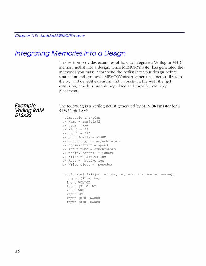
Integrating Memories into a DesignThis section provides examples of how to integrate a Verilog or VHDL memory netlist into a design. Once MEMORYmaster has generated the memories you must incorporate the netlist into your design before simulation and synthesis. MEMORYmaster generates a netlist file with the .v, .vhd or .edif extension and a constraint file with the .gcf extension, which is used during place and route for memory placement.
ExampleVerilog RAM512x32
The following is a Verilog netlist generated by MEMORYmaster for a 512x32 bit RAM:
'timescale 1ns/10ps// Name = ram512x32// type = RAM// width = 32// depth = 512// part family = A500K// output type = asynchronous// optimization = speed// input type = synchronous// parity control = ignore// Write = active low// Read = active low// Write clock = posedge
module ram512x32(DO, WCLOCK, DI, WRB, RDB, WADDR, RADDR);output [31:0] DO;input WCLOCK;input [31:0] DI;input WRB;input RDB;input [8:0] WADDR;input [8:0] RADDR;
10

Integrating Memories into a Design
GND U1(.Y(VSS));RAM256x9SA M0(.WCLKS(WCLOCK), .DO8(n27), .DO7(n24), .DO6(n21),.DO5(n18),.....//memory blocks instantiation
endmodule
The following is an example of how to instantiate a ram512x32 module into a design:
ram512x32 MY_RAM_INST(.DO(data_out),.WCLOCK(clk),.DI(data_in), .WRB(wrb), .RDB(rdb),.WADDR(write_add),.RADDR(read_add));
After instantiating the memory into the Verilog source code, the next step is to simulate and synthesize the design. Before synthesizing the design, make sure that the “dont_touch” attribute is set on all memories generated by MEMORYmaster. Refer to the ProASIC Interface Guide or the documentation included with your synthesis tool for additional information on how to apply a “dont_touch” attribute on a memory block.
VHDL RAMExample
The following is a VHDL example of the previously generated memory:
-- Name = ram512x32-- type = RAM-- width = 32-- depth = 512-- part family = A500K-- output type = asynchronous-- optimization = speed-- input type = synchronous-- parity control = ignore-- Write = active low-- Read = active low-- Write clock = posedge
11
Chapter 1: Embedded MEMORYmaster
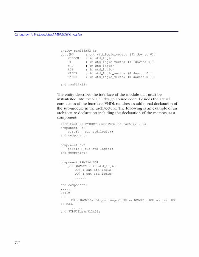
entity ram512x32 isport(DO : out std_logic_vector (31 downto 0);
WCLOCK : in std_logic;DI : in std_logic_vector (31 downto 0);WRB : in std_logic;RDB : in std_logic;WADDR : in std_logic_vector (8 downto 0);RADDR : in std_logic_vector (8 downto 0));
end ram512x32;
The entity describes the interface of the module that must be instantiated into the VHDL design source code. Besides the actual connection of the interface, VHDL requires an additional declaration of the sub-module in the architecture. The following is an example of an architecture declaration including the declaration of the memory as a component:
architecture STRUCT_ram512x32 of ram512x32 iscomponent PWR
port(Y : out std_logic);end component;
component GNDport(Y : out std_logic);
end component;
component RAM256x9SAport(WCLKS : in std_logic;
DO8 : out std_logic;DO7 : out std_logic;......
);end component;......begin......
M0 : RAM256x9SA port map(WCLKS => WCLOCK, DO8 => n27, DO7=> n24,
......end STRUCT_ram512x32;
12
Integrating Memories into a Design
Importing theNetlist intoASICmaster
After synthesis, a design is translated into either a Verilog, VHDL, or an EDIF netlist. The netlist includes all logic blocks as well as the memories. To import the netlist file(s) into ASICmaster, refer to the ASICmaster User’s Guide. Placement information generated by MEMORYmaster must be imported into ASICmaster as constraints. This allows ASICmaster to place the memories.
The following is an example placement constraints file:
memory ram512x32 (memory_blocks (
( M7 M5 M3 M1 )( M6 M4 M2 M0 )
))
M0 through M7 are the memory blocks instantiated into the generated netlist. While placing the entire design, ASICmaster looks for the macro “ram512x32” in the constraints file. If it finds a block in the netlist with the same name, it looks for M0, M1 etc in that block and places them serially. If you want to place memory in any other way, use manual memory placement.
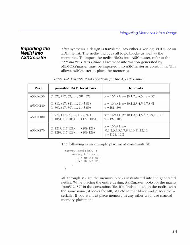
Table 1-2. Possible RAM Locations for the A500K Family
Part possible RAM locations formula
A500K050 (1,57), (17, 57), ..., (81, 57) x = 16*n+1; n= {0,1,2,3,4,5}; y = 57;
A500K130(1,81), (17, 81), ..., (145,81) (1,89), (17, 89), ..., (145,89)
x = 16*n+1; n= {0,1,2,3,4,5,6,7,8,9}y = {81, 89}
A500K180(1,97), (17,97), ..., (177, 97)(1,105), (17,105), ..., (177, 105)
x = 16*n+1; n= {0,1,2,3,4,5,6,7,8,9,10,11}y = {97, 105}
A500K270(1,121), (17,121), ..., (209,121)(1,129), (17,129), ..., (209,129)
x = 16*n+1; n= {0,1,2,3,4,5,6,7,8,9,10,11,12,13}y = {121, 129}
13
Chapter 1: Embedded MEMORYmaster
Note: If you use the previous memory modules in a synthesis flow, make sure that you set “dont_touch” attributes on the modules generated by MEMORYmaster. Otherwise, the names of these modules may be changed and ASICmaster cannot find the memory modules to be placed in the netlist.
ManualMemoryPlacement
For manual placement, a .gcf constraints file must be created. The following is an example of a manually created placement file for a A500K130 device.
set_location (1,81) <hier_instance_name>/M0;set_location (1,89) <hier_instance_name>/M1;set_location (33,89) <hier_instance_name>/M2;set_location (33,81) <hier_instance_name>/M3;
The (x,y) coordinates are device dependent. If wrong coordinates are entered, ASICmaster reports about wrong coordinates and displays a list of valid coordinates for the selected device. Refer to Table 1-2 on page 13 for valid coordinates for each device.
Embedded Memory ExamplesThis section provides examples of how to generate memory and integrate it into your design. These examples also briefly explain simulation, synthesis and place and route for each example.
Example 1-Two PortMemory
This example demonstrates how to generate a two port RAM that is 1024 words deep by 8 bits wide with synchronous write and asynchronous read and an even parity generation and how to integrate it into a design.
Generate the Memory
1. Invoke ASICmaster.
2. Click the Tools button. The ASICmaster tools dialog box is displayed.
3. Click Build Embedded Memories.
14

Embedded Memory Examples
4. (PC Only) You must first set a working directory for your design and click the Select button as shown in Figure 1-6 on page 9. The MEMORYmaster main window is displayed (see Figure 1-2 on page 5).
5. Click the New button. Specify the name of memory in the name box. Use “mem1024x8” for this example.
6. Specify RAM as the Type.
7. Specify Synchronous as the Write Access.
8. Specify Asynchronous as the Read Access.
9. Type 1024 as the Depth and 8 as the Width.
10. Specify Generate Even as the Parity. The MEMORYmaster main window should appear as in Figure 1-7.
11. (Optional) Click the Port Tab to assign special names to memory ports.
12. Click the Generate button.
Figure 1-7. MEMORYmaster Main Window
15

Chapter 1: Embedded MEMORYmaster
Instantiate the Memory into a Designmodule top_level(in, out, clk, reset....);input in, clk, reset;output out;....
// instantiate memorymem1024x8 MEM1(.DI(wr_data), .DO(rd_data)....);
//rest of the design codealways@(posedge clk or negedge reset )
begin....
end;endmodule
Simulate and Synthesize
After instantiating a memory into the design, simulate and synthesize it. Memory models are included into the simulation and synthesis libraries. Refer to the documentation included with your simulation and synthesis tools for additional information. During synthesis make sure that the “dont_touch” attribute is set on all memories generated by MEMORYmaster.
Place and RouteAfter synthesis, a netlist is written out that contains the embedded memories and the logic of a design. For automatic placement, use the constraints file (mem1024x8.gcf) generated by MEMORYmaster. If automatic placement is used, memories are placed in a line and can be placed and routed in ASICmaster. For manual placement, create a text file similar to the following, and read this file into ASICmaster:
set_location (1,81) MEM1/M0;set_location (17,81) MEM1/M1;set_location (33,81) MEM1/M2;set_location (49,81) MEM1/M3;
Memory blocks can be in any legal position. See Table 1-2 on page 13 for legal position of memory blocks.
16

Embedded Memory Examples
Example 2-512x16 FIFO
This example demonstrates how to generate an asynchronous FIFO that is 512 deep by 16 wide with FULL, EMPTY, and HALF FULL flags, no parity checking or generation, and how to integrate it into a design.
Generate the FIFO
1. Invoke ASICmaster.
2. Click the Tools button. The ASICmaster tools dialog box is displayed.
3. Click Build Embedded Memories.
4. (PC Only) You must first set a working directory for your design and click the Select button as shown in Figure 1-6 on page 9. The MEMORYmaster main window is displayed (see Figure 1-2 on page 5).
5. Specify all required fields for the design. Specify static as the FIFO Trigger Level and half depth(256) for the programmable flags. Enter width and depth. Select FIFO under Type field.
6. Click generate.
Instantiate the FIFO into the designmodule top_level (in,out, clk,reset ....);input in ....;........
// instantiate fifoFIFO512x16 rec_fifo(.DI(wr_data), .DO(rd_data)....);always@(posedge clk or ....) // rest of the design code........
endmodule
Simulate and SynthesizeAfter instantiating a FIFO into the design, simulate and synthesize it. Memory models are included in the simulation and synthesis libraries. Refer to the documentation included with your simulation and synthesis tools for additional information. Make sure that the “dont_touch” attribute is set on all memories generated by MEMORYmaster.
17

Chapter 1: Embedded MEMORYmaster
Place and RouteAfter synthesis, a netlist is written out that contains the embedded memories and the logic of a design. For automatic placement, use the constraints file (FIFO 512x16.gcf) generated by MEMORYmaster. If automatic placement is used, memories are placed in a line and can be placed and routed in ASICmaster. For manual placement, create a text file similar to the following, and read this file into ASICmaster:
set_location (1,81) rec_fifo/MO;set_location (17,81) rec_fifo/M1;set_location (33,81) rec_fifo/M2;set_location (49,81) rec_fifo/M3;
Memory blocks can be in any legal position. See Table 1-2 on page 13 for legal position of memory blocks.
18

2Distributed MEMORYmaster
This chapter describes the distributed memory architecture and how to use the Distributed MEMORYmaster to create distributed memories for ProASIC device.
Distributed Memory ArchitectureDistributed memory can be generated as a two port asynchronous register file or as an asynchronous FIFO. Distributed memories are made up of the logic tiles of the device. These memory files are netlists consisting of logic tiles and do not use to embedded memory cells.
The RegisterFile
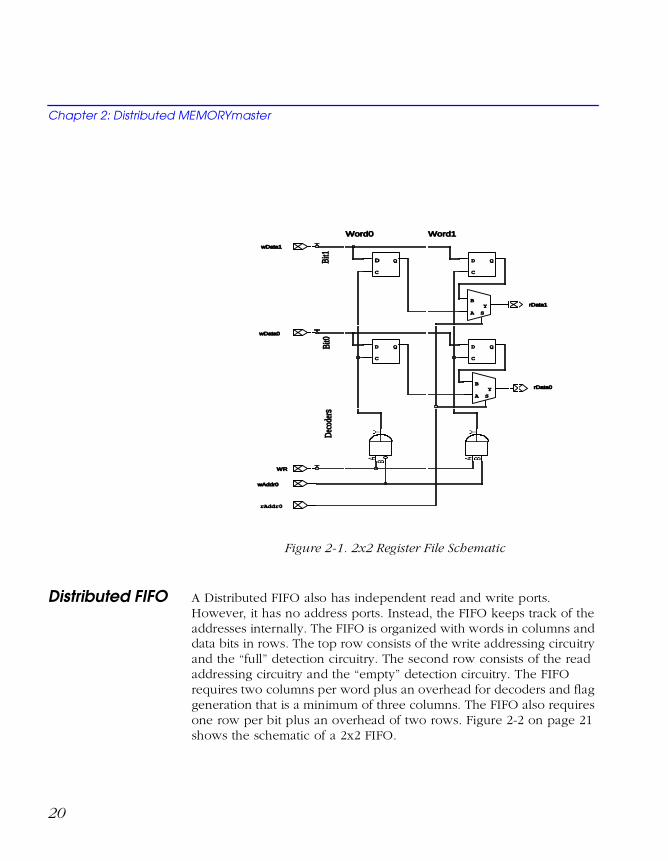
The register file has independent read and write ports. The read port is asynchronous so the read data is not clocked and is available a short time after the read address changes. The write port is also asynchronous and data is written on the active edge of WR. The write operation can be either level sensitive or edge-sensitive. The schematic of a 2x2 memory is shown in Figure 2-1 on page 20. The schematic is marked to show the words (vertical slices), the bits (horizontal slices) and the decoders (one per word). The register file memory requires 1 column per word and 2 rows per bit plus from 1 to 3 rows for the necessary decoders.
19
Chapter 2: Distributed MEMORYmaster
Figure 2-1. 2x2 Register File Schematic
Distributed FIFO A Distributed FIFO also has independent read and write ports. However, it has no address ports. Instead, the FIFO keeps track of the addresses internally. The FIFO is organized with words in columns and data bits in rows. The top row consists of the write addressing circuitry and the “full” detection circuitry. The second row consists of the read addressing circuitry and the “empty” detection circuitry. The FIFO requires two columns per word plus an overhead for decoders and flag generation that is a minimum of three columns. The FIFO also requires one row per bit plus an overhead of two rows. Figure 2-2 on page 21 shows the schematic of a 2x2 FIFO.
D
C
Q
D
C
Q
D
C
Q
D
C
Q
B
A S
Y
B
A S
Y
wData1
wData0
WR
wAddr0
rAddr0
rData1
rData0
Word0 Word1
Bit0
Dec
oder
sBi
t1
20

Distributed Memory Architecture
Figure 2-2. 2x2 FIFO Schematic
DeterminingTile Usage
ProASIC parts tend to have more tiles horizontally. The choice of orientation affects the allowable size of the memory. A horizontal memory allows the maximum possible number of words. A vertical memory allows the maximum number of bits per word. MEMORYmaster can create register files of up to 64 words on any possible ProASIC device. Distributed memories are created using logic tiles and are generally slower and larger compared to embedded RAM. Actel recommends that larger memories be implemented with
D
C
SQ
AB
Y
AB
Y
Init
Write
Read
D Q
D Q
wData1
wData0
D
C
SQ
AB
Y
AB
Y
D Q
D Q
D
C R
Q
D
C R
Q
AB
Y
AB
Y
D Q
D Q
D
C R
Q
D
C R
Q
rData1
rData0
AB
Y
AB
Y
AB
Y
AB
Y
AB
Y
AB
Y
empty
full
21
Chapter 2: Distributed MEMORYmaster
embedded memory. The maximum distributed FIFO sizes in any ProASIC device is 80 words. The maximum RAM and FIFO sizes are shown in Table 2-1.
1. Numbers in parentheses are for FIFOs.
The orientation of the register file affects how it is placed. Horizontal register files are placed with words in columns and bits in rows as shown in Figure 2-3.
Figure 2-3. Horizontal Memory
Table 2-1. Maximum RAM and FIFO Dimensions
Device Vertical Horizontal
Words Width Words Width
A500K050 64 (23)1 46 (94) 64 (36) 30 (62)
A500K130 64 (29) 78 (158) 64 (62) 38 (78)
A500K180 64 (36) 95 (192) 64 (75) 46 (94)
A500K270 64 (45) 110 (222) 64 (80) 58 (118)
Decoders
Core2 * number bits per word
number of words
22

Distributed Memory Architecture
Vertical memories are placed with bits in columns and words in rows as shown in Figure 2-4.
Figure 2-4. Vertical Memory
The decoder sizes are given in table Table 2-2.
Table 2-2. Decoder Sizes
Number of Words
Decoder Size
2 ~ 4 1
5 ~ 8 2
9 ~ 64 3
Dec
oder
s
Cor
e
2 * number bits per word
num
ber
ofw
ords
23

Chapter 2: Distributed MEMORYmaster
CalculatingLogic Usage
The following section presents how to calculate logic usage for Memory area, and a vertical and a horizontal memory.
Memory Area
The following is an example of how to calculate memory area:
Memory Area = Number of Words (2 * Number of bits +decoder size)
Vertical Orientation
The following is an example logic usage calculation for a 16x32 RAM:
Width in tiles = 2 * number-of-Bits-per-word + decoder size
= 2 * 32 + 3 = 67
Height in tiles = number-of-words = 16
Horizontal OrientationThe following is a an example logic usage calculation for a 16x32 RAM:
Tiles in Width = Number-of-Words = 16
Tiles in Height = 2 * number-of-bits-per-word + decoder size
= 2 * 32 + 3 = 67
MEMORYmaster displays the legal coordinates to place the memory if the macro is not rotated or flipped. The horizontal could be placed between the coordinates (1,1) and (145, 15) assuming the A500K130 device was selected.
DistributedMemoryPlacement
To achieve the best timing and efficient placement, use the placement constraints file generated by the Distributed MEMORYmaster. For more information on constraint statements, refer to the ASICmaster User’s Guide. To utilize this file, use the “set_location” constraint statement for macros. For example:
set_location (x,y) <mem_hier_name> <macro_name>;
24

Distributed Memory Generation and Instantiation
DistributedMemory Timing
Memory timing values are dependent on the memory size and the routing to and from the memory. Since the memories are implemented as ProASIC primitives, users can determine the timing characteristics of the circuit by performing a back annotated timing analysis. In fact, to the timing analyzer, the distributed memory looks like any other part of the circuit and requires no special treatment. “Timing for Distributed Memories” on page 29, explains the critical timing paths in each memory, and why these paths are critical.
Distributed Memory Generation and InstantiationConsider the following hierarchical design, which instantiates a 16x32 memory as shown in Figure 2-5.
Figure 2-5. Design Example
Figure 2-6 shows how to generate a RAM of 16x32 with MEMORYmaster. Use the generated file to instantiate the RAM into your design.
TOP
block1 block2
ram16x32 block3
U1 U2
U3mem_inst
25

Chapter 2: Distributed MEMORYmaster
Figure 2-6. Distributed MEMORYmaster User Interface
Welcome to ASICmaster's Distributed MEMORYmaster VersionV5p2(C) 1996-1999 Gatefield Corporation. All rights reserved.Note: See the MEMORYmaster User Guide for detailed
information about this program and how to use it.Please enter output format:
1 for verilog2 for vhdl ?1
Type of module:1 for 2-port asynchronous register file2 for fifo0 to quit? 1
Type of device:1 for A500K0502 for A500K1303 for A500K1804 for A500K2700 to quit?1
Orientation of memory:1 for horizontal2 for vertical0 to quit? 2
Cell name? ram16x32Number of words (2...64)? 16Number of data bits per word (2...46)? 32Memory type:
'e' for edge triggered,'l' for level-sensitve? e
Generating verilog file "ram16x32.v" in "/home1/users"Generating gcf file "ram16x32.gcf" in "/home1/users"Legal X: (1...31)Legal Y: (1...49)Done.Type <cr> to close the window.
26

Distributed Memory Generation and Instantiation
Simulation and SynthesisAfter instantiating a memory into the design, simulate and synthesize it. Memory models are included into the simulation and synthesis libraries. Refer to the documentation included with your simulation and synthesis tools for additional information. During synthesis make sure that the “dont_touch” attribute is set on all memories generated by MEMORYmaster.
Place and Route
After synthesis, a netlist is written out that contains the embedded memories and the logic of a design. For automatic placement, the ram16x32.gcf constraints file generated by MEMORYmaster must be imported into ASICmaster and a statement similar to the following must also be included in a constraint file submitted to ASICmaster:
set_location (10,10) U1/mem_inst mem16x32;
ASICmaster treats the memory as a macro and places it in a rectangle with the bottom-left corner on tile coordinate (10,10). Memory can be moved on the die by changing this coordinate.
Note: Distributed memory contains very high fanout nets so, if you do not use the above placement constraints, memory timing will be sub-optimal or the design may not route.
27


3Timing for Distributed Memories
The following chapter decribes the timing parameters for the level sensitive register file, and edge-triggered register file. It also includes information about edge-triggered FIFOs.
Level-sensitive Register FileThe level-sensitive register file has three main timing parameters.
• Tacc - time from stable read-address to output data valid
• Tsetup_data - time from stable write-data to falling edge of WR
• Tsetup_addr - time from stable write-address to rising clock edge
Figure 3-1 shows the timing of these parameters:
Figure 3-1. Level-sensitive Mode Timing Diagram
rAddr
rData
wData
wAddr
WR
Tacc
Tsetup_data
Tsetup_addr
29

Chapter 3: Timing for Distributed Memories
Failure to meet these timing values will have the following results:
• Tacc - read data might be from previous address
• Tsetup_data - data may not be written into the memory
• Tsetup_addr - data may be written into some other address as well as the intended address
Edge-triggeredRegister File
The edge-triggered register file has three main timing parameters:
• Tacc - time from stable read-address to output data valid
• Tsetup_data - time from stable write-data to rising WR edge
• Tsetup_addr - time from stable write-address to rising WR edge
Figure 3-2 shows the relationships of the signals.
Figure 3-2. Edge-triggered Mode Timing Diagram
rAddr
rDataTacc
wData
wAddr
WR
Tsetup_data
Tsetup_addr
30

Level-sensitive Register File
Failure to meet these timing values will have the following results:
• Tacc - read data might be from previous address
• Tsetup_data - data may not be written into the memory
• Tsetup_addr - data may be written into some other address
The main advantage of the edge-triggered memory is that the write timing is sensitive only to the rising edge of the WR, not both the rising and falling edges.
Edge-triggeredFIFO
The edge-triggered FIFO captures data on the rising edge of the “WR” signal, and the read pointers advance on the rising edge of the “RD” signal. Before using the FIFO, it must be initialized by pulsing the “INIT” signal high. Immediately after initialization, the “empty” signal is true and the “full” signal false. Data applied on the “wDataX” signals are captured when the “WR” signal transitions from 0 to 1. Simultaneously, the “empty” signal will become false to indicate that there is valid data on “rDataX.” Further transitions from 0 to 1 on “WR” captures more data into the FIFO until such time as “full” becomes true. At this point, the FIFO is full, and no more data should be entered into it.
After the FIFO is initialized, the output data remains invalid until the first read operation is performed. With every rising edge of the read pulse, the FIFO generates the next word written into it on the output data bus until all the words written into it are read out. At this point the “empty” signal goes high. Further read operations produce no change to the data output as it remains fixed at the last word written into the FIFO.
31
Chapter 3: Timing for Distributed Memories
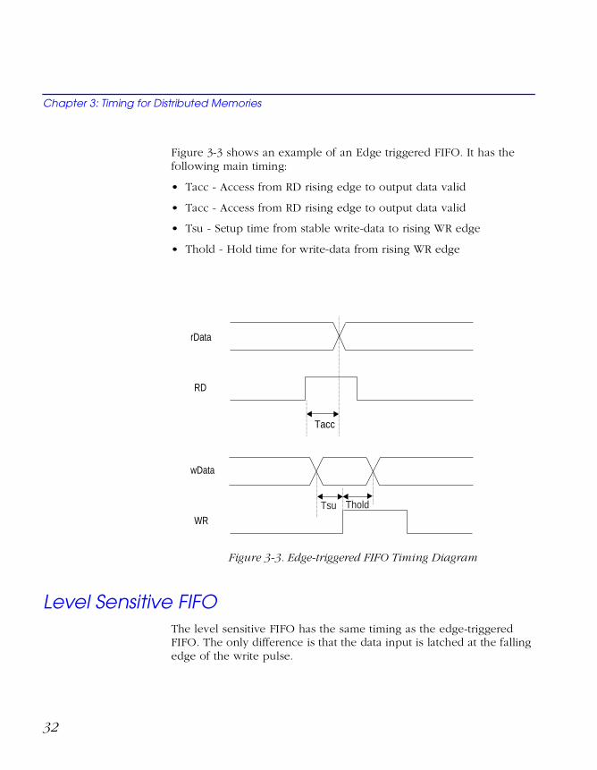
Figure 3-3 shows an example of an Edge triggered FIFO. It has the following main timing:
• Tacc - Access from RD rising edge to output data valid
• Tacc - Access from RD rising edge to output data valid
• Tsu - Setup time from stable write-data to rising WR edge
• Thold - Hold time for write-data from rising WR edge
Figure 3-3. Edge-triggered FIFO Timing Diagram
Level Sensitive FIFOThe level sensitive FIFO has the same timing as the edge-triggered FIFO. The only difference is that the data input is latched at the falling edge of the write pulse.
Tacc
rData
RD
wData
WRTsu Thold
32
4Using Multiple Memories in a Design
This chapter describes how to use multiple memories in a design. If a design includes several memories with different sizes and access modes, Actel recommends generating them all in one session of MEMORYmaster. The embedded memories are automatically generated and are accompanied by placement directives. ASICmaster uses these directives to place the memories efficiently.
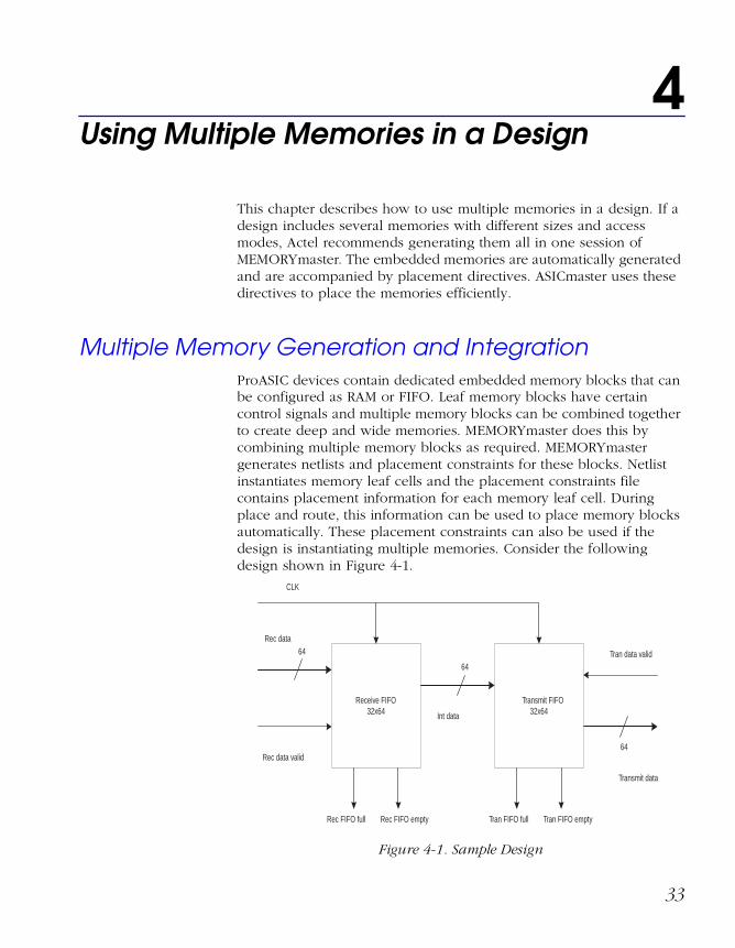
Multiple Memory Generation and IntegrationProASIC devices contain dedicated embedded memory blocks that can be configured as RAM or FIFO. Leaf memory blocks have certain control signals and multiple memory blocks can be combined together to create deep and wide memories. MEMORYmaster does this by combining multiple memory blocks as required. MEMORYmaster generates netlists and placement constraints for these blocks. Netlist instantiates memory leaf cells and the placement constraints file contains placement information for each memory leaf cell. During place and route, this information can be used to place memory blocks automatically. These placement constraints can also be used if the design is instantiating multiple memories. Consider the following design shown in Figure 4-1.
Figure 4-1. Sample Design
Receive FIFO32x64
Transmit FIFO32x64
Rec data64
64
CLK
Rec data valid
Int data
64
Tran data valid
Transmit data
Tran FIFO emptyTran FIFO fullRec FIFO full Rec FIFO empty
33

Chapter 4: Using Multiple Memories in a Design
In this design, there is a receive FIFO and transmit FIFO. Read and Write ports are synchronous. Each FIFO is 32 words deep and 64 bits wide. Also, both FIFOs are identical. Only one FIFO needs to be created with MEMORYmaster, and it must be instantiated twice into the design. The MEMORYmaster window that illustrates how to create this FIFO is shown in Figure 4-2.
Figure 4-2. MEMORYmaster Window Showing a Sample FIFO
Once the FIFO is generated with MEMORYmaster, it must be instantiated into the design. The following is an example of the RTL after instantiation:
module top(tran_data, rec_data, rec_data_valid,tran_data_valid, clk, reset, rec_fifo_full,rec_fifo_empty, tran_fifo_full, tran_fifo_empty);// this is top level module
input rec_data_valid, clk, reset, tran_data_valid;output[63:0] tran_data;output rec_fifo_full, rec_fifo_empty,tran_fifo_full,tran_fifo_empty;input[63:0] rec_data;
34

Multiple Memory Generation and Integration
wire[63:0] data_int;/* Receiver FIFO instantiation */sync_fifo rec_FI(.data_in(rec_data),.data_out(data_int),
.wr(rec_data_valid), .rd(1'b0),
.empty(rec_fifo_empty), .full(rec_fifo_full),
.reset(reset), .clk(clk));/* transmit FIFO instantiation */sync_fifo tran_FI(.data_in(data_int),
.data_out (tran_fifo_full)
.wr(1'b0), .rd(tran_data_valid),
.empty(tran_fifo_empty), .full(tran_fifo_full),
.reset(reset), .clk(clk));/* other RTL of the design and other blocks */
endmodule
module sync_fifo (data_in, data_out, wr, rd, empty, full,reset, clk);input[63:0] data_in;output[63:0] data_out;input wr, rd,clk, reset;output empty, full;/* Instantiation of FIFO generated from MEMORYmaster */fifo32x64 F1(.DO(data_out), .RCLOCK(clk), .WCLOCK(clk),
.DI(data_in), .WRB(wr), .RDB(rd), .RESET(reset),
.FULL(full), .EMPTY(empty), .EQTH(), .GEQTH());
endmodule
35

Chapter 4: Using Multiple Memories in a Design
Simulate andSynthesize
Now the design can be simulated and synthesized. The following is an example of a Verilog-XL simulation command:
verilog test_sim.v top.v fifo32x64.v –v$AMHOME/etc/deskits/verilog/lib/A500K.v
The following is a typical Design Compiler script for synthesis of a design including memory blocks:
read –format verilog fifo32x64set_dont_touch find(design, “fifo32x64”) /* memories must bedont_touch during synthesis */read –format verilog top.vcreate_clock –period 20 clk /* add timing constraints */set_wire_load A500Kset_operating_conditions WORSTcompileset_port_is_pad “*” /* use set_pad_type to to use a particulartype of pad */insert_padswrite –format verilog –hierarchy –output top_str.v /* writeout netlist with hierarchy */quit
MemoryPlacement
The netlist “top_str.v”contains both FIFO instantiations and can be used for post synthesis gate level simulation. After synthesis, you can place and route the design. If there are multiple instances of the same memory, ASICmaster automatically determines that the same constraints file applies to all memories. So, place and route should be run with “top_str.v” as a netlist and “fifo32x64.gcf” as a constraints file. In this example, each FIFO uses 8 memory blocks. ASICmaster attempts to place each FIFO in a line. The resulting placement on an A500K130 device, which has 20 memory slots, is shown in Figure 4-3 on page 37. For information about the Layout Viewer, refer to the ASICmaster User’s Guide.
36

Multiple Memory Generation and Integration
Figure 4-3. Sample Memory Placement
During placement ASICmaster attempts to keep one memory entity in one group. In the example shown in Figure 4-3 on page 37, it placed the “Rec_FI/F1/M0” in the first memory slot on the left side of the lower row, and “rec_FI/F1/M1” in next slot and so on. Only ten slots were available in one row and therefore, the placement of “tran_FI” started from the upper row. If each memory block had used four blocks, both memory blocks would be placed one after another in the lower row.
M7M4M6M7 M2
M5M3
M3M1 M4M2M0M1 M0M5
M6
8 blocks of tran_FI
8 blocks of Rec_FI
37

Chapter 4: Using Multiple Memories in a Design
Manual Placement of Multiple MemoriesA memory placement file must be created to manually place memories. For example, to place the “rec_FI” from the previous example on the left side using both rows and the “tran_FI” on right side in both rows, the following placement file would be used:
set_location (1,81) rec_FI/F1/M0;set_location (1,89) rec_FI/F1/M1;set_location (17,89) rec_FI/F1/M2;set_location (17,81) rec_FI/F1/M3;set_location (33,81) rec_FI/F1/M4;set_location (33,89) rec_FI/F1/M5;set_location (49,89) rec_FI/F1/M6;set_location (49,81) rec_FI/F1/M7;
set_location (145,81) tran_FI/F1/M0;set_location (145,89) tran_FI/F1/M1;set_location (129,89) tran_FI/F1/M2;set_location (129,81) tran_FI/F1/M3;set_location (113,81) tran_FI/F1/M4;set_location (113,89) tran_FI/F1/M5;set_location (97,89) tran_FI/F1/M6;set_location (97,81) tran_FI/F1/M7;
This constraints file should be read into ASICmaster and would result in the placement shown in Figure 4-4 on an A500K130 device.
Figure 4-4. Sample FIFO Placement
M1 M6M5M2 M1M2M5M6
M0 M7M4M3 M0M3M4M7
Tran FIFORec FIFO
38

Manual Placement of Multiple Memories
MEMORYmaster generates constraint files for each memory. All of these files should be read into ASICmaster during place and route. ASICmaster determines the placement for each memory and keeps each memory entity together. For automatic placement of memories, Actel recommends that all constraint files from MEMORYmaster be read into ASICmaster. To change default placement, you can discard constraints from MEMORYmaster and create your own for memory placement.
Glue Logic forWider orDeeperMemories
If very deep or very wide memories are created, MEMORYmaster combines together multiple blocks and uses glue logic to combine them. Two lists quantifying glue logic are shown in Table 4-1 and Table 4-2 on page 40 .
These tables cover extreme cases of depth or width for RAMs and FIFOs for the A500K130 device, which offers 20 memory blocks and 12800 logic tiles.
Table 4-1. RAM
RAM ParityMemory Blocks Used
Logic Tile Used
Comment
Depth 5120 Width 8
Check Even 20 259All 20 blocks used in depth
Depth 256 Width 160
Check Even 20 22All 20 blocks used in width
39

Chapter 4: Using Multiple Memories in a Design
For FIFOs, MEMORYmaster creates placement directives for glue logic. If placement information from MEMORYmaster is used, glue logic placement is more efficient.
Programmable Flags in FIFOsProASIC devices provide programmable flags for FIFOs. The threshold for these flags can be set in MEMORYmaster in the main menu, shown in Figure 1-7 on page 15. It is on the bottom right corner in the FIFO Trigger Level box. You can specify whether the flag is static or dynamic. If dynamic is selected, MEMORYmaster will create a FIFO with a LEVEL bus on the memory interface. You can apply values in the range of 0 to 255 to this bus to change its threshold dynamically.
The overall trigger level is a multiple “d,” which is the number of used basic memory blocks in depth (each 256 words). The increment between each overall trigger level is equal to “d.” For example, a memory that is 512 words deep is built up of two basic memory block in depth (512/256). The highest almost full trigger level should be assigned, which is 510 (512-d = 512-2) The corresponding dynamic trigger LEVEL is 255 (510/n = 510/2).
Table 4-2. FIFO
FIFO ParityMemory Blocks Used
Logic Tile Used
Comment
Depth 5120 Width 8
Check Even 20 592All 20 blocks used in depth
Depth 256 Width 160
Check Even 20 62All 20 blocks used in width
40
Programmable Flags in FIFOs
If the threshold is not changing, you can select the static option and specify the threshold value. In this case, MEMORYmaster will hardwire threshold to the specified value. A detailed timing of these flags can be found in the ProASIC 500k Family Datasheet.
Note: Trigger level is also called threshold. Consequentally, equal threshold (EQTH) and greater equal threshold (GEQTH) are the names of the trigger flags.
41


AProduct Support
Actel backs its products with various support services including Customer Service, a Customer Applications Center, a Web and FTP site, electronic mail, and worldwide sales offices. This appendix contains information about using these services and contacting Actel for service and support.
Actel U.S. Toll-Free LineUse the Actel toll-free line to contact Actel for sales information, technical support, requests for literature about Actel and Actel products, Customer Service, investor information, and using the Action Facts service.
The Actel Toll-Free Line is (888) 99-ACTEL.
Customer ServiceContact Customer Service for non-technical product support, such as product pricing, product upgrades, update information, order status, and authorization.
From Northeast and North Central U.S.A., call (408) 522-4480.From Southeast and Southwest U.S.A., call (408) 522-4480.From South Central U.S.A., call (408) 522-4434.From Northwest U.S.A., call (408) 522-4434.From Canada, call (408) 522-4480.From Europe, call (408) 522-4252 or +44 (0) 1256 305600.From Japan, call (408) 522-4743.From the rest of the world, call (408) 522-4743.Fax, from anywhere in the world (408) 522-8044.
43

Appendix A: Product Support
Customer Applications CenterThe Customer Applications Center is staffed by applications engineers who can answer your hardware, software, and design questions.
All calls are answered by our Technical Message Center. The center retrieves information, such as your name, company name, phone number and your question, and then issues a case number. The Center then forwards the information to a queue where the first available application engineer receives the data and returns your call. The phone hours are from 7:30 a.m. to 5 p.m., Pacific Standard Time, Monday through Friday.
The Customer Applications Center number is (800) 262-1060.
European customers can call +44 (0) 1256 305600.
Guru Automated Technical SupportGuru is a Web based automated technical support system accessible through the Actel home page (http://www.actel.com/guru/). Guru provides answers to technical questions about Actel products. Many answers include diagrams, illustrations and links to other resources on the Actel Web site. Guru is available 24 hours a day, seven days a week.
Web SiteActel has a World Wide Web home page where you can browse a variety of technical and non-technical information. Use a Net browser (Netscape recommended) to access Actel’s home page.
The URL is http://www.actel.com. You are welcome to share the resources we have provided on the net.
Be sure to visit the “Actel User Area” on our Web site, which contains information regarding: products, technical services, current manuals, and release notes.
44

FTP Site
FTP SiteActel has an anonymous FTP site located at ftp://ftp.actel.com. You can directly obtain library updates, software patches, design files, and data sheets.
Electronic MailYou can communicate your technical questions to our e-mail address and receive answers back by e-mail, fax, or phone. Also, if you have design problems, you can e-mail your design files to receive assistance. The e-mail account is monitored several times per day.
The technical support e-mail address is [email protected].
45

Appendix A: Product Support
Worldwide Sales Offices
HeadquartersActel Corporation955 East Arques AvenueSunnyvale, California 94086Toll Free: 888.99.ACTEL
Tel: 408.739.1010Fax: 408.739.1540
US SalesOffices
California
Bay AreaTel: 408.328.2200Fax: 408.328.2358
IrvineTel: 949.727.0470Fax: 949.727.0476
San DiegoTel: 619.938.9860Fax: 619.938.9887
Thousand OaksTel: 805.375.5769Fax: 805.375.5749
Colorado
Tel: 303.420.4335Fax: 303.420.4336
Florida
Tel: 407.677.6661Fax: 407.677.1030
Georgia
Tel: 770.831.9090Fax: 770.831.0055
Illinois
Tel: 847.259.1501Fax: 847.259.1572
Maryland
Tel: 410.381.3289Fax: 410.290.3291
Massachusetts
Tel: 978.244.3800Fax: 978.244.3820
Minnesota
Tel: 612.854.8162Fax: 612.854.8120
North Carolina
Tel: 919.870.8996Fax: 919.870.8257
Pennsylvania
Tel: 215.830.1458Fax: 215.706.0680
Texas
Tel: 972.235.8944Fax: 972.235.9659
International SalesOffices
CanadaSuite 203135 Michael Cowpland Dr,Kanata, Ontario K2M 2E9
Tel: 613.591.2074Fax: 613.591.0348
France361 Avenue General de Gaulle92147 Clamart Cedex
Tel: +33 (0)1.40.83.11.00Fax: +33 (0)1.40.94.11.04
GermanyLohweg 2785375 Neufahrn
Tel: +49 (0)8165.9584.0Fax: +49 (0)8165.9584.1
Hong KongSuite 2206, Parkside Pacific Place, 88 Queensway
Tel: +011.852.2877.6226Fax: +011.852.2918.9693
ItalyVia Giovanni da Udine No. 3420156 Milano
Tel: +39 (0)2.3809.3259Fax: +39 (0)2.3809.3260
JapanEXOS Ebisu Building 4F1-24-14 Ebisu Shibuya-kuTokyo 150
Tel: +81 (0)3.3445.7671Fax: +81 (0)3.3445.7668
Korea135-090, 18th Floor, Kyoung Am Building157-27 Samsung-dongKangnam-ku, Seoul
Tel: +82 (0)2.555.7425Fax: +82 (0)2.555.5779
Taiwan4F-3, No. 75, Sec. 1,Hsin-Tai-Wu Road,Hsi-chih, Taipei, 221
Tel: +886 (0)2.698.2525Fax: +886 (0)2.698.2548
United KingdomDaneshill House,Lutyens CloseBasingstoke,Hampshire RG24 8AG
Tel: +44 (0)1256.305600Fax: +44 (0)1256.355420
46

Index
AActel
FTP Site 45Web Based Technical Support 44Web Site 44
CConfiguration tab 6Contacting Actel
Customer Service 43Electronic Mail 45Technical Support 44Toll-Free 43Web Based Technical Support 44
Customer Service 43
DDistributed MEMORYmaster 19
EElectronic Mail 45Embedded Memory Configurations 2Embedded MEMORYmaster 1
FFIFO 20
IIntroduction ix
MMemory Architecture 19Memory Placement 24
NNaming Conventions 2
PProduct Support 43–46
Customer Applications Center 44Customer Service 43Electronic Mail 45FTP Site 45Technical Support 44Toll-Free Line 43Web Site 44
RRAM Locations 13Resource Usage 7
TTechnical Support 44The Distributed FIFO 21The Register File 19Toll-Free Line 43
WWeb Based Technical Support 44
47