Embed Size (px)
DESCRIPTION
MIT Radiation Laboratory Series, Pulse Generators - Volume 5, 1947
Citation preview

CHAPTER 1
INTRODUCTION
BY G. N. GLASOE
Microwave radar has required the development of pulse generatorsthat are capable of producing a succession of pulses of very short time dura-tions. The pulse generators of a radar system fall into two principalcategories, namely, those that are associated with the transmitter andthose that are used in the indicator and ranging circuits. The principaldistinguishing feature of pulse generators of these two types is the outputpower level. The radar transmitter requires the generation of high-powerand high-voltage pulses whereas the indicator and ranging circuitsrequire pulses of negligible power and relatively low voltage. The pur-pose of this book is to record information that pertains to the basic prin-ciples underlying the design of power pulse generators. Although mostof these principles have been developed primarily in the field of microwaveradar, they are equally adaptable to a very large number of applicationsnot associated with radar. The discussion is general, and reference tospecific microwave-radar applications is made only when they serve asexamples of attainable results. Specific design information is given forsome of the practicable circuits that have been built and have proved tobe satisfactory.
The most commonly used source of the high-frequency energy that isnecessary for microwave radar has been the magnetron oscillator. Theproblem of power-pulse-generator design has, therefore, been greatlyinfluenced by the characteristics of these magnetron oscillators. Byvirtue of this application many of the basic principles of pulse-generatordesign are better understood.
The power pulse generators used in the transmitters of radar systemshave been variously referred to as “modulators,” ‘‘ pulsers,” and (‘key-ers.” Since the function of these generators is to apply a pulse of voltageto an oscillator and thereby produce pulses of high-frequency energy tobe radiated by the antenna, the term ‘‘ pulser “ is a descriptive abbrevia-tion for pulse generator. Throughout this book, therefore, the term“ pulser” will be used in preference to the terms ‘( modulat or” and“keyer.”
1.1. Parameters Fundamental to the Design of Pulse Generators.—There are certain parameters of a pulser that are common to all types
m

2 ZNTRODUCTIOX [SEC.1.1
and that affect the design. The most important of these parametersare pulse duration, pulse power, average power, pulse recurrence fre-quency, duty ratio, and impedance level. Before proceeding to thedetailed discussion of pulser design, therefore, it is well to introduce theparameters by defining some terms and indicating the ranges which havebeen common in the microwave-radar field.
In its broadest aspects, the term “pulse duration” is the time duringwhich a voltage or current maintains a value different from zero or someother initial and final value. The term “ pulse shape” is used to referto the form obtained when the pulse amplitude is plotted as a function oftime. When referring to such a plot, it is convenient to discuss the detailsof a particular pulse shape in terms of the “leading edge,” the “top,”and the “trailing edge” of the pulse. If a pulse of voltage or current istruly rectangular in shape, that is, has a negligible time of rise and falland is of constant amplitude for the intervening time interval, the pulseduration is simply the time elapsed between the deviation from and thereturn to the initial value. The term “negligible time” is, of course,relative and no strict boundaries can be attached. For most practicalpurposes, however, if the rise and fall times for a pulse are about a tenthor less of the pulse duration, the pulse is considered substantially rec-tangular. A current pulse of this type is required for a magnetron oscil-lator by virtue of the dependence of the output frequency on the current,which is called the “pushing factor. ” For pulses which are definitelynot rectangular, the effective or equivalent pulse duration is either thetime measured at some fraction of the maximum pulse amplitude that issignificant to the particular application, or the time corresponding to arectangular equivalent of the pulse in question. The interpretation ofpulse duration is discussed in Appendix B, and when particular casescome up in the text they are considered in more detail.
The pulsers that have been designed for microwave-radar applica-tions have pulse durations covering the range of 0.03 to 5 ~sec. Thedesign of a pulser for short pulse durations with substantially rectangularpulse shape requires the use of high-frequency circuit techniques sincefrequencies as high as 60 to 100 hlc/sec contribute to the pulse shape andthe effects of stray capacitances and inductances become serious.
In the microwave-radar field the voltage required across the magnet-ron ranges from as 10]v as 1 kv to as big-h as 60 kv. If a voltage pulse isapplied to some type of ciissipative load, a magnetron for example, therewill be a corresponding pulse of current which depends on the nature ofthis load. The pulse current through the magnetron ranges from a fewamperes to several hundred amperes. The combined considerations ofshort pulse duration and rectangularity therefore require that carefulattention be given to the behavior of the pulser circuit and its components
SEC.1.1] FUNDAMENTAL DESIGN PARAMETERS 3
under conditions of high rates of change of voltage and current. Thrrate of change of voltage may be as high as several hundred kilovoltsper microsecond, and the current may build up at the rate of hundreds tothousands of amperes per microsecond.
The product of the pulse voltage and the pulse current is the pulsepower. When the voltage and current pulses are rectangular, the cor-responding pulse power is unambiguous. When the pulses are irregularlyshaped, however, the meaning of the term “pulse power” is not so clearbecause somewhat arbitrary methods are often used to average the prod-uct of voltage and current during the pulse. The peak power of a pulseis the maximum value of the product of the voltage and current. Thus,for rectangular pulses the peak power and the pulse power are the same,but for irregularly shaped pulses the peak power is greater than the pulsepower.
In this connection’ there are two general types of load that are dis-cussed most frequently, namely, the linear load, such as a pure resist ante,and the nonlinear load, such as the magnetron. The magnetron loadcan be approximately represented as a biased diode with a dynamicresistance that is low and a static resistance that is about ten times higher.Static resistance is the ratio of the voltage across the load to the current,through the load, whereas the dynamic resistance is the ratio of a smallchange in voltage to the corresponding change in current. When thedynamic resistance of the load is small, the magnitude of the pulse cur-rent varies greatly with only small variations of the pulse voltage, and forloads such as a magnetron, for example, the behavior of the pulser with alinear load is not necessarily a good criterion.
Since the pulse-power output of pulsers for microwave-radar applica-tion has ranged from as low as 100 watts to as high as 20 Mw, the averagepower output as well is important to the design. The average powercorresponding to a particular pulse power depends on the ratio of theaggregate pulse duration in a given interval to the total time, and this inturn depends on the pulse recurrence frequency, PRF, which is the num-ber of pulses per second (pps). If the pulse duration is 7 and the timebetween the beginning of one pulse and the beginning of the next pulseis T,, then
()P., = ; PD.,- = ,( PRF)Pp . . . .1’
A similar equation can be written in terms of the current if the pulsevoltage is essentially constant during the time corresponding to the cur-rent pulse, thus

4 INTRODUCTION [SEC.1.1
Since the average current and the PRF are relatively easy to measure,this relation may be used to define a pulse current if the top of the pulseis irregular but the rise and fall times are negligibly small. It may alsobe used to define an equivalent pulse duration for a pulse shape that istrapezoidal and perhaps rounded at the top, but l\here some significancecan be attached to a pulse-current measurement.
The ratio T/T,—or the product 7(1’RF)—is commonly called thepulser “ duty, “ ‘f duty cycle, ” or preferably “ duty ratio, ” and is expressedas a fraction or a percentage. Thus l-psec pulses repeated at a rate of1000 pps correspond to a duty ratio of 0.001 or 0.1 per cent. Pulsershave been constructed ~vith a duty ratio as high as 0.1, but for most radarapplications a value of 0.001 or lolver is most common. As ~vith anypower device, the over-all efficiency of a pulser is an important considera-tion in its design. This is particularly true ]Vhen the average po~ver out-put is high, that is, a combination of high pulse power and high dutyratio. This point is stressed in the discussion and is frequently a decid-ing factor in choosing one type of pulser in preference to another.
The pulse recurrence frequency affects the design of a pulser in waysother than from the standpoint of the po~rer considerations. The pulsercircuit may be considered to have a quiescent state that is disturbedduring the pulse interval and to \rhich it must return before the initiationof the next succeeding pulse. If the PRF is very high, the problem ofreturning the circuit to this quiescent state becomes of importance.Such things as time constants and deionization times may impose alimit on how small the interpulse interval can be \vithout unduly com-plicating the design. This limit becomes especially important \rheneverit is necessary to produce a series of closely spaced pulses to form a codesuch as is used in radar beacons.
The choice of the internal impedance of the pulse generator dependson the load impedance, the pulse-pol’:er level, and practical considera-tions of circuit elements. Impedance-matching betlreen generator andload is of prime importance in some cases, especially with regard to theproper utilization of the available energy and the production of a particu-lar pulse shape. Impedance-matching is not always convenient with theload connected directly to the pulser output; hoirever, matching canreadily be attained by the use of a pulse transformer. By this means it ispossible to obtain impedance transformations between pulser and loadas high as 150/1, that is, a transformer with a turns ratio of about 12/1.The magnetrons ~~-hichha~,e been used in micro~va~,e radar have staticimpedances ranging from about 400 ohms to ahout 2000 ohms; in general,the higher the power of the magnetron, the lower its input impedance.
The impedance-transformation characteristic of the pulse transformeralso provides a means of physically separating the pulser and the load.

Srsc.1.2] THE BASIC CIRCUIT OF A PULSE GENERATOR 5
Thus the power may be transmitted from the pulser to the load through alow-impedance coaxial cable, provided that pulse transformers are usedto match impedances. For most efficient power transfer such impedance-matching is necessary between pulser and cable and between cable andload. In this way it has been possible to transmit high-power pulses ofshort duration over as much as 200 ft of cable without a serious loss inthe over-all eficiency or a deterioration of the pulse shape.
The pulse transformer has another function that is important to pulserdesign, namely, it provides a means for reversing the polarity of a pulse.This feature of the pulse transformer together with the impedance-transformation property considerably extends the range of usefulness forpulsers of any type.
1.2. The Basic Circuit of a Pulse Generator.—The pulse generatorsdiscussed in this book depend on the storage of electrical energy eitherin an electrostatic field or in a magnetic field, and the subsequent dis-charge of a fraction or all of this stored energy into the load. The twobasic categories into which the largest number of pulser designs logicallyfall are (1) those in which only a small fraction of the stored electricalenergy is discharged into the load during a pulse, and (2) those in whichall of the stored energy is discharged during each pulse. These two basiccategories of pulsers are generally referred to as (1) “hard-tube pulsers”and (2) “line-t ype pulsers. ”
To accomplish this discharge, it is necessary to provide a suitableswitch that can be closed for a length of time corresponding to the pulseduration and maintained open during the time 1 trequired to build up the stored energy again be-
!__J
Energy-fore the next succeeding pulse. In its simplest storage L
device Switchform, therefore, the discharging circuit of apulser can be represented schematically as shownin Fig. 1.1. The characteristics required for the
Load
switch will be different depending on whether ornot all the stored energy is discharged into the FIG.1.1.—Brwicdischmg-load during a single pulse. Some pulse-shaping ing circuitof a puker.
will be necessary in the discharging circuit when all the energy is to bedissipated.
Since the charging of the energy-storage component of the pulsertakes place in the relatively long interpulse interval, the discussion ofpulsers may logically be divided into the consideration of the dischargingcircuit on the one hand, and the charging circuit on the other. Powersupplies for ,these pulsers are, in general, of conventional design andtherefore usually need not be discussed, but wherever this designhas bearing on the over-all pulser behavior, special mention is madeof the fact.

6 INTRODUCTION [SEC.1.3
1.3. Hard-tube Pulsers.-In general, the energy-storage device fortheee pulsers is simply a condenser that is charged to some voltage V,thus making available an amount of electrical energy +CV2. The term“hard-tube” refers to the nature of the switch, which is most commonlya high-vacuum tube containing a control grid. The closing and openingof this switch is therefore accomplished by applying properly controlledvoltages to the grid. Since only a small fraction of the energy stored inthe condenser is discharged during the pulse, the voltage across theswitch immediately after the pulse and during the charging interval isnearly the same as it is at the beginning of the pulse. It is thereforenecessary that the grid of the vacuum-tube switch have complete controlof the conduction through the tube. This required characteristic of theswitch tube rules out the possibility of using known gaseous-dischargedevices for this type of pulser.
It is generally desired that these pulsers produce a succession of pulses,and therefore some provision must be made to replenish the charge onthe storage condenser. This is accomplished by means of a power supplywhich is connected to the condenser during the interpulse interval. The
Isolatingelement
Powersupply
Charging Discharging
p!k “rc”” -4
T[
Storagecondenser
Load=1-
Switch
I 1 JFIG.I.Z.—Chargingand dischargingcircuit
for a hard-tubepulser.
combination of the dischargingand charging circuits of the pulsermay be represented schematicallyas shown in Fig. 1.2. In order toavoid short-circuiting the powersupply during the pulse interval,some form of isolating elementmust be provided in series withthe power supply. This elementmay be a high resistance or aninductance, the particular choicedepending on the requirements ofover-all pulser design. The pri-mary consideration is to keep the~ower-sumdv current as small as
possible during the pulse interval. However, th~ ~m-pedance of this isolat-ing element should not be so high that the voltage on the condenser at theend of the interpulse interval differs appreciably from the power-supplyvolt age.
Because of the high pulse-power output, pulsers for microwave radarrequire switch tubes that are capable of passing high currents for theshort time corresponding to the pulse duration with a relatively smalldifference in potential across the tube. Oxide-cathode and thoriated-tungsten-filament tubes can be made to pass currents of many amperesfor the pulse durations necessary in the microwave-radar applications

SEC.1.3] HA RD-TUkE PULSERS 7
with a reasonable operating life expectancy. The cathode efficiency,that is, amperes of plate current per watt of heating power, is consider-ably less for the thoriated-tungsten filament than for the oxide cathode.For switch tubes with oxide cathodes it has been common to obtainabout 0.3 to 0.5 amp/watt of heating power, although as much as 1amp/watt has been obtained, whereas for thoriated-tungsten filamentsthis amount is generally less than 0.1 amp/watt. The tungsten-filamenttube, however, is less subject to sparking at high voltages and currentsand, within Radiation Laboratory experience, these tubes have notexhibited cathode fatigue, that is, a falling-off of cathode emission duringlong pulses. This cathode fatigue is sometimes a limitation on the long-est pulse for which an oxide-cathode switch tube should be used.
In order to obtain a high plate current in these switch tubes, theremust be a fairly high positive voltage on the control grid and thereforeconsiderable grid current. In the case of a tetrode, there is a high screen-grid current as well The duty ratio permitted in a given pulser is oftenlimited by the amount of average power which the particular tube candissipate.
The output circuit of a hard-tube pulser does not usually contain anyprimary pulse-shaping components, although its design, in combinationwith the load, has a marked effect on the ultimate shape of the pulse.In a pulser of this type, the pulse is formed in the driver circuit, the out-put of which is applied to the control grid of the switch tube. From thestandpoint of over-all pulser efficiency, it is desirable that the switchtube be nonconducting during the interpulse interval. The control gridmust therefore be at a voltage sufficiently negative to keep the tube cutoff during this time, and consequently the output voltage from the drivermust be sufficient to overcome this grid bias and carry the grid positive.For most designs of hard-tube pulsers, this requirement means that thedriver output power must be a few per cent of the actual pulser outputpower.
The resistance of available vacuum tubes used as switches in hard-tube pulsers ranges from about 100 to 600 ohms. If the pulser is con-sidered as a generator with an internal resistance equal to that of theswitch tube, the highest discharge efficiency is obtained when the effectiveload resistance is high. Matching the load resistance to the internalresistance of the pulser results in an efficiency of 50 per cent in the outputcircuit and the switch tube must dissipate as much power as the load.Because of these considerations, the hard-tube pulser is generally designedwith a power-supply voltage slightly greater than the required pulsevoltage. This design practice has not been followed when the outputvoltage required is higher than the power-supply voltage that is easilyobtainable. The power-supply voltage may be limited by available

8 I,YTRODUCTION [SEC.1.4
components, size requirements, and other special considerations. Apulse transformer may then be used between the pulser and the load toobtain the desired pulse voltage at the load.
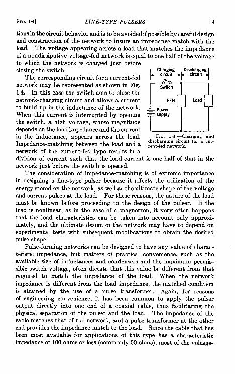
1.4. Line-type Pulsers.—Pulse generators in this category are referredto as ‘‘ line-type” pulsers because the energy-storage device is essentiallya lumped-constant transmission line. Since this component of the line-type pulser serves not only as the source of electrical energy during thepulse but also as the pulse-shaping element, it has become commonlyknolvn as a “ pulse-forming net!vork,” PFX. There are essentially twoclasses, of pulse-forming netlvorks, namely, those in w-hich the energy forthe pulse is stored in an electrostatic field in the amount +CVZ, and thosein n-hich this energy is in a magnetic field in the amount +512. The firstclass is referred to as “ voltage-fed networks” and the second as “current-fed networks. ” The voltage-fed network has been used extensively inthe microivave-radar applications in preference to the current-fed net-\vork because of the lack of satisfactory s!vitch tubes for the latter type.
The pulse-forming net!vork in a line-type pulser consists of induc-tances and condensers ~rbich may be put together in any one of a numberof possible configurations. The configuration chosen for the particularpurpose at hand depends on the ease with which the network can befabricated, as \vell as on the specific pulser characteristic desired. TheI’alues of the inductance and capacitance elements in such a network canbe calculated to give an arbitrary pulse shape when the configuration,pulse duration, impedance, and load characteristics are specified. Thetheoretical basis for these calculations and the detailed discussion of the
o role of the various network parameters are givenin Part II of this book.
The discharging circuit of a line-type pulserPFN using a voltage-fed network may be represented
Switch schematically as shown in Fig. 1“3. If energyhas been stored in the network by charging the
Load capacitance elements, closing the switch willallow the discharge of this energy into the load.When the load impedance is equal to the charac-
FIG. 1.:l.—lli,rtl~rgi]lg teristic impedance of the network, assuming thecucuit for a voltage-fed switch to have negligible resistance, all of theIlet\Y,,lk.
energy stored in the network is transferred tothe load, leaving the condensers in the network completely discharged.‘l’he time required for this energy transfer determines the pulse durationand depends on the values of the capacitances and inductances of the net-\rork. If the load impedance is not equal to the network impedance, someenergy will be left on the rwtnwrk at the end cf the time corresponding tothe pulse duration for the matched load. This situation leads to complica-
SEC. 14] LINE-TYPE PULSERS 9
tions in the circuit behavior and is to be avoided if possible by careful designand construction of the network to insure an impedance match with theload. The voltage appearing across a load that matches the impedanceof a nondissipative voltage-fed network is equal to one half of the voltag(to which the network is charged just beforeclosing the switch.
The corresponding circuit for a current-fednetwork may be represented as shown in Fig.1.4. In this case the switch acts to close thenetwork-charging circuit and allows a currentto build up in the inductance of the network.When this current is interrupted by openingthe switch, a high voltage, whose magnitudedepends on the load impedance and the currentin the inductance, appears across the load.Impedance-matching between the load and anetwork of the current-fed type results in a
t
Charging
“rc”” +F;W
III
r
Switch
PFN Losd
~ Power= supply
FIG. 1.4.—Ch8rginganddischargingcircuit for a CUr-rent-fednetwork.
division of current such that ~he load current is one half of that in thenetwork just before the switch is opened.
The consideration of impedance-matching is of extreme importancein designing a line-type pulser because it affects the utilization of theenergy stored on the network, as well as the ultimate shape of the voltageand current pulses at the load. For these reasons, the nature of the loadmust be known before proceeding to the design of the pulser. If theload is nonlinear, as in the case of a magnetron, it very often happensthat the load characteristics can be taken into account only approxi-mately, and the ultimate design of the network may have to depend onexperimental tests with subsequent modifications to obtain the desiredpulse shape.
Pulse-forming networks can be designed to have any value of charac-teristic impedance, but matters of practical convenience, such as theavailable size of inductances and condensers and the maximum permis-sible switch voltage, often dictate that this value be different from thatrequired to match the impedance of the load. When the networkimpedance is different from the load impedance, the matched conditionis attained by the use of a pulse transformer. Again, for reasonsof engineering convenience, it has been common to apply the pulseroutput directly into one end of a coaxial cable, thus facilitating thephysical separation of the pulser and the load. The impedance of thecable matches that of the network, and a pulse tra~sformer at the otherend provides the impedance match to the load. Since the cable that hasbeen most available for applications of this type has a characteristicimpedance of 100 ohms or less (commonly 50 ohms), most of the voltage-

10 INTRODUCTION [SEC. 1.4
fed lin~type pulsers for microwave radar have been designed for the50-ohm level, thereby making the use of a pulse transformer a necessitywith magnetron load. The pulse transformer therefore becomes anessential part of the discharging circuit in a low-impedance pulser usedwith high-impedance load, and as such its characteristics have an effecton the pulse shape and the over-all behavior of the discharging circuit.It is desirable and often necessary that the design of the pulse transformerand the design of the pulse-forming network be coordinated in order toobtain the most satisfactory pulser operation.
Since the impedance-transformation ratio for a transformer is equalto the square of the voltage-transformation ratio, the use of a low-impedance pulser with a load of higher impedance requires the use of apulse transformer that gives a voltage stepup between pulser output andload input. Thus, when a line-type pulser with a 50-ohm voltage-fednetwork is used to pulse an 80&ohm load, for example, the voltagestepup ratio is about 4/1, and the current in the discharging circuit ofthe pulser becomes about four times the load current. Accordingly, theswitch in the discharging circuit of a line-type pulser is required to passvery high pulse currents for high pulse power into the load. Since theswitch is in series with the pulser output, its effective resistance must besmall compared with the characteristic impedance of the pulse-formingnetwork if high efficiency is desired.
When a pulser uses a voltage-fed network, the voltage across theswitch falls to zero at the end of the pulse because the stored energy iscompletely discharged. This consideration, in conjunction with thehigh current-carrying capacity and low resistance required of the switch,suggests the use of a form of gaseous-discharge device, which must remainnonconducting during the interpulse interval if it is desired to apply asuccession of pulses to the load. If it is also required that the interpulseintervals be of controlled duration, the switch must have a furthercharacteristic which allows a positive control of the time at which con-duction is initiated. These switch requirements can be met by rotaryspark gaps, which depend on overvolting by a decrease in the gap length,or by fixed spark gaps, in which the discharge is initiated by an auxiliaryelectrode. A grid-controlled gaseous-discharge tube such as the thyra-tron is particularly well suited to this application since it is possible tostart the discharge in a tube of this type at any desired time, within avery small fraction of a microsecond, by the application of Pi oper voltageto the grid. Several grid-controlled hydrogen-filled thyratrons of dif-ferent voltage and current ratings that cover the range of pulse-poweroutput from a few kilowatts to almost two megawatts have been devel-oped for this application. These hydrogen thyratrons have proved tobe very practical switches for line-type pulsers because they fulfill ade-

SEC.1.4] LINE-TYPE PULSERS 11
quately all the switch requirements mentioned above and have a stabilityagainst ambient temperature variations that is considerably better thanthat of the mercury thyratron. Hydrogen thyratrons that have asatisfactory operating life and yet can hold off 16 kv with the grid atcathode potential and carry pulse currents of several hundred amperesfor a pulse duration of 2 psec and a recurrence frequency of 300 pps havebeen developed and manufactured.
The grid-controlled high-vacuum tube is not well suited to serve asthe switch in a low-impedance line-type pulser using a voltage-fed net-work because of its rather low cathode efficiency and relatively highresistance during the conduction period. An oxide-cathode high-vacuumtube that requires 60 watts of cathode-heater power, for example, cancarry a pulse current of about 15 amp for a pulse duration of a few micro-seconds, and under these conditions, this tube presents a resistance ofperhaps 100 ohms to the circuit. A hydrogen thyratron, on the otherhand, with equivalent cathode-heater power can carry a pulse current ofabout 300 amp, presenting an effective resistance to the circuit of aboutone ohm.
As stated previously, a line-type pulser using a curren~fed networkrequires a switch capable of carrying a current at least twice thatdesired in the pulser load. The further requirement that this switchmust be capable of interrupting this current. and withstanding high volt-age during the pulse eliminates the gaseous-discharge type and points tothe grid-controlled high-vacuum tube. The low current-carrying capac-ity of existing tubes has, therefore, been the principal deciding factor inchoosing the voltage-fed network for line-type pulsers rather than thecurrent-fed network.
Several different methods are usedto charge a voltage-fed network in aline-type pulser. Since the generalaspects of these methods are not ap-preciably affected by the dischargingcircuit, the requirements imposed onpulser design by the charging circuitcan be considered separately. If thetime allowed for the charging of thenetwork is sufficiently long comparedwith the pulse duration, the chargingcycle is simply that corresponding tothe accumulation of charge on a con-
Isolatingelement
Powersupplya’PFN Switch
= Load=
FIO.1.5.—Chargingand dischargingcir-cuit for a voltage-fednetwork.
denser. Figure 1.5 indic~tes schematically the relation between the charg-ing and discharging circuits of a pulser with voltage-fed network. Forexample, the network may be recharged from a d-c power supply through
12 INTRODUCTION [SEC.1.4
a high resistance, in which case the equilibrium voltage on the networkcan be nearly equal to the power-supply voltage. The requirement on theseries-resistance isolating element in this charging circuit is simply thatit must be large enough to allow only negligible current to be taken fromthe power supply during the pulse and the deionizing time for the switch,but not so large that the RC time constant becomes comparable to theinterpulse interval. To get the highest network voltage from a givenpower-supply voltage with this arrangement, the length of the interpulseinterval should be several times greater than the RC time constant in thecharging circuit. This method of charging the network is inherentlyinefficient-its maximum possible efficiency is only 50 per cent.
Since the efficiency of the network-charging circuit with a resistanceas the isolating element is very low, the use of a nondissipative element,such as an inductance, suggests itself. When a capacitance is chargedthrough an inductance from a constant potential source, the voltageacross the capacitance is in the form of a damped oscillation the firstmaximum of which is approximately equal to twice the supply voltage ifthe initial voltage across the capacitance and the current through theinductance are zero. This maximum occurs at a. time equal to z ~after the voltage source is connected to the inductance-capacitancecombination. The inductance to be used with a given network is, there-fore, calculated by setting the interpulse interval equal to T ~, whereC is the network capacitance. This type of network charging is called“resonant charging.” If the pulse recurrence frequency is less thatl/ir ~, some current will still be flowing in the inductance at thebeginning of each charging period and, under equilibrium conditions, thisinitial current will be the same for all charging cycles. The network willagain be charged to approximately twice the power-supply voltage. This
. type of network charging is called “linear charging. ”With careful design of the inductance, the efficiency of the charging
circuit is as high as 90 to 95 per cent, and the power-supply voltage needsto be only slightly greater than one half of the desired network voltage,resulting in a great advantage over resistance charging. A factor of 1.9to 1.95 between network and supply voltage can be obtained if thecharging inductance is designed so that the quality factor Q of the charg-ing circuit is high.
Resonant charging can also be done from an a-c source providedthat the pulse recurrence frequency, PRF, is not greater than twice thea-c frequency. If the pulse recurrence frequency and the a-c frequencyare equal, the network voltage attains a value r times the peak a-c volt-age. This voltage stepup becomes greater as the ratio of a-c frequencyto pulse recurrence frequency increases. The voltage gain soon becomesexpensive, however, and it is not practical to go beyond an a-c frequencygreater than twice the PRF.
SEC. 1.5] COMPARISON 13
1.5, A Comparison of Hard-tube and Line-type Pulsers.—Althoughit is not possible to give a set of fixed rules to be followed in determiningthe type of pulser best suited to a particular application, it is possible togive a few general comparisons of the two types which may aid in choos.ing between them. The comparisons made here concern such things as:power output and efficiency, pulse shape, impedance-matching, shortinterpulse intervals, high-voltage versus low-voltage power supply, theease with which pulse duration and pulse recurrence frequency can bechanged, time jitter, over-all circuit complexity, size and weight of thepulsers, and regulation of the pulser output against variations in inputvoltage. This list does not include all the possible points for compari-son, but only those that are of primary importance in choosing betweenthe two pulser types.
The over-all efficiency of the line-type pulser is generally somewhathigher than that of the hard-tube pulser, particularly when the pulse-power output is high. This is due in part to the fact that the hard-tubepulser requires a larger overhead of cathode-heating power. Further-more, a high-vacuum-tube switch dissipates a greater portion of theavailable pulser power by virtue of its higher effective resistance thandoes a gaseous-discharge switch. The power required for the driver ofthe hard-tube pulser is not negligible and, since this component is notnecessary in a line-type pulser, the over-all efficiency of the latter isthereby enhanced.
The pulse shape obtained from a hard-tube pulser can usually bemade more nearly, rectangular than that from a line-type pulser. Thisis particularly true when the network of the pulser has low impedance,and a pulse transformer must be used between the pulser and a nonlinearload such as a magnetron. In this case, small high-frequency oscilla-tions are superimposed on the voltage pulse at the load. These oscil-lations make the top of the pulse irregular in amplitude. The amplitudeof the corresponding oscillations on the top of the current pulse dependson the dynamic resistance of the load and, if this is small, these oscilla-tions become an appreciable fraction of the average pulse amplitude.The hard-tube pulser is, therefore, generally preferred to the line-type forapplications in which a rectangular pulse shape is important.
Impedance-matching between pulser and load has already beenmentioned as an important consideration in the design of line-type pul-SSrs. Usually, an impedance mismatch of ~ 20 to 30 per cent can betolerated as far as the effect on pulse shape and power transfer to the loadk concerned, but a greater mismatch causes the over-all pulser operationto become unsatisfactory. The load impedance of the hard-tube pulser,however, can be changed over a wide range without seriously affectingthe operation. The principal limitation in the latter case is that, if theload impedance is too low, the required current through the switch tube
14 I,YTROL)l ‘C TIO.I’ [SEC. 1.5
is l:irge :in(l the power dissipated in the switch becomes a larger fractiont)f the t{Jt:d po\rcr, thus lo!rering the efficiency. In applications of theIinu-typr pulser it is possible to effect an impedance match for any loadby the proper choice of pldse tr:msfurmcr, but this procedure is sorneu-hatinconvenient if, for example, it is desired to vary the po~ver input to anonlinear load bctjveen }vidc limits.
S\vitchcs of the gaseous-discharge type, ~vhich are commonly used inthe line-type pulser, place a stringent limitation on the minimum spacingbCt\YCCIlpulses. After the pulse, the net\rork must not charge up to anyappreciable voltage until the deionization is complete, otherwise theslvitch ]~ill remain in the conducting state and the po!ver supply \vill beshort-cirmlitcd. For this reason, the interpulsc interval must be severaltimes :1s long M the slritch deionization time \vhcn the gaseous-dischargetype is (MY1. ‘l’he high-vacuum-tube s\vitch in the hard-tube pulser doesnot, prment any similar limitations on the intcrpulsc interval, but in thiscase the problcm bccomcs one of designing the circuit ~vith small RC and1./1/ time constants. It has been possible, for example, to constructhar(l-tube pulsers \vith 0,2-~sec pulses spacccl 0.8 ~sec bet~reen leadingedges,
It has been stated in the preceding discussion of hard-tube pulsersthat a high-voltage po\vcr supply is necessary for highest efficiency.‘I’his rcquircrncnt is sometimes a very serious limitation on the design ofsuch pulscrs for high-pulse-polvcr output. The low-irnpcdance line-typepulser using resonant charging of the network, on the other hand, can bedesigned with a much lolrer pow-er-supply voltage for a pulse-poweroutput comparable to that of a hard-tube pulser. For example, a hard-tubc pulscr \vith a pulse-po~vcr output of 3 MW has been built with a35-kv po~rer sllpply, ~vhcrcas for a line-type pulser with d-c resonantcharging of the net\vork, the same po\\-eroutput is obtained with onlyabout 14 kv from the pofvcr supply if a standard 50-ohm net!vork is used.,~ line-type pulscr using a-c resonant charging, on the other hand, requiresan a-c po\~m source giving a peak voltage of about 8 kv in order to providea pulse-po\rcr output of 3 31w. It should bc stated, ho~vever, that inboth of the line-type pulscrs mentioned here the pulse-forming networksarc charged to about 25 kv, but this voltage does not present such seriousdesign problems from the engineering standpoint as the design of a powersupply of equivalent voltage. It Jvould have been advantageous tohave a poi~-cr-supp]y voltage greater than 35 kv for this 3-MJv hard-tubepulsrr, I)llt a higher voltage \vas impractical because the pulscr designNW limited by the available components, in particular by the s\vitchtul)e.
[t is somctirncs desirable to have a pulscr capable of producing pulsesof scvcrd different durations, the particular one to bc used being selected

r
SEC.1.5] COMPA RIA’ON 15
by a simple switching operation. The pulse duration is determined inthe driver of the hard-tube pulser, where this type of pulse selection iseasily made since the switching can be done in a lo~v-voltage part of thecircuit. In the line-type pulscr, holvcvcr, the pulse duration is deter-minedby the netlvork and in order to change the pulse duration a differentnetwork must be connected into the circuit. This can be accomplishedby a switching operation, but because of the higher voltage involved it isnot so simple as in the hard-tube pulser. A further complication mayarisein the line-type pulser since a change of network affects the character-istics of the charging circuit, ancl practical considerateions of induct antecharging therefore limit the ranges of pulse duration and pulse recur-rence frequency that can be covered. The ease with which the pulseduration may be changed in a hard-tube pulser provides a flexibility thatis difficult to obtain with a line-type pulser.
In many pulser applications it is important to have the interpulseintervals precisely determined. In hard-tube pulsers and some line-typepulsers,constant interpulse intervals are obtained by using a trigger pulseto initiate the operation of the pulser. These trigger pulses can be gener-ated in a lowpo~rer circuit independent of the pulser, and it is a simplematter to design such a circuit so that the trigger pulses occur at pre-cisely known time intervals. l~hen the successive output pulses fromthe pulser start with varying time delay after the start of the triggerpulse, there is said to be time jitter in the output pulses. If the triggerpulses are used to initiate the operation of other apparatus, which isauxiliary to the pulser, this time jitter results in unsatisfactory over-alloperation ot’ the equipment. Hard-tube pulsers can be easily designedto make this time jitter negligible, that is, = 0.02 gsec or less. The timejitter is also small in line-type pulsers that make use of a hydrogen thyra-tron as the slvitch. lVith line-type pulsers using the triggered sparkgaps (series gaps), however, the time jitter is considerably greater, about0.1 to 3 Kscc depending on the gap design. Recent development of atriggered spark gap having a cathode consisting of spongy iron saturatedwith mercury has made it possible to obtain time jitter as small as 0.02psecwith the series-gap switch. tVhen a rotary spark gap is used as theswitch in a line-type puker, the interpulse intervals are determined bythe rotational speed and the number of sparking electrodes. In thiscase time jitter refers to the irregularity of the interpulse intervals andmay amount to as much as 20 to 80 ysec.
Because the circuit for the hard-tube pulser is somewhat more com-plex and requires a larger number of separate components than that ofthe line-type pulser, both the problem of servicing and the diagnosisof faulty behavior of the hard-tube pulser are more difficult. Because ofthe combination of fewer separate components and higher efficiency, a

16 INTRODUCTION [SEC.I 5
Iinc-type pukwr can generally be designed for smaller size and weight thana hard-tube pulser \vith equivalent pulse- and average-po\~er output andwith comparable safety factors in the individual components.
TABLE1 1.—COMPARISONOFTHETwo PULSERTYPES
Characteristics
JMiciency. . . . . . . . . .
Pulseshape. . . . . . . . .
Impedarl{:c-rllatching
Interpulseinterval..
Voltagesupply. . . . .
Changeof pulseclura.tion
Time jitter.
Circuitcomplexity..
IMccts of change ilvoltage
llard-tube pulser
Lower; more overhead powerrequiredfor the driver,cath-ode-heating,and for dissipa.tion in the switchtube
Betterrectangularpulses
}Vide rangeof mismatchper-missible
May be very short; as for coding beacons (i.e., < 1 pscc)
High-voltage supply usuallynecessary
Easy; switchingin low-voltagtcircuit
Somewhat easier to obtainnegligible time jitter (i.e.,< 0.02 psec) than with aline-typepulser
~reatcr, leading to greaterdifficultyin servicing
For design having maximumcfficicncy, (AP/P) output =6(3 V/J’) input. By sacrificingefficiencyin thedesign,(ti’/~) output = 0.5(AV/Vinput can be obtained
Line-type pulser
tfigh, particularly when thepulse-po,veroutput is high
Poorerrectangularpulse, par-ticularlythroughpulsetrans-former
Smaller range of mismatchpermissible ( +20 to 3070).Pulsetransformerwill matchany load, but power input tononlinear load cannot bevaried over a wide range
Must be several times thedeionization time of dis-chargetube (i.e., > 100@cc)
Low-voltage supply, particu-larly with inductance charg-ing
Requireshigh-voltage switch-ing to new network
lligh-pOwer line-type pulserswith rotary-gap switch haveaninherentlylargetimejitter;with care in design and theuse of a hydrogen thyratronor enclosedgaps of mercury-sponge type, a time jitter of0.02 ~ec is obtainable
Less, permitting smaller sizeand weight
Betterthana hard-tubepulserdesigned for maximum effi-ciency since (A~/~) output= 2(AV/V) input for a line-type pulser, independent ofthe design
The effect on the power output of a pulser resulting from a change inthe input voltage is sometimes of considerable importance to the particu-lar application. For a line-type pulser, the percentage change in outputpower is about two times the percentage change in input line voltage, and
1
SEC.1.5]
little can be done to change
COlfPA RISON 17
this ratio appreciably. In the case of the..hard-tube pulser, hoirevw, this ratio m~y be controlled by the properchoice of the s!vitcb tube and its operating conditions. The percentagechange in output polver from a hard-tube pulser may be varied over therange of 0.5 to 6 times the percentage change in input line voltage. Thisadvantage with the hard-tube pulser is gained only at the expense oflower efficiency, hoircver, and the ratio is large when the dischargingcircuit is designed for maximum efficiency.
These comparisons between hard-tube and line-type pulsers aresummarized in Table 1’1.
It should be evident from these general remarks concerning the rela-tive merits of hard-tube and line-type pulsers that a perfunctory analysisof the requirements for a particular application cannot lead to an intel-ligent choice of the pulser type to be used. A detailed analysis requires athorough understanding of the characteristics of pulsersin general, andof the two types in particular. It is the purpose of the following chapters,therefore, to present the available information on hard-tube and line-type pulsers in considerable detail in order that it may be of the great-est possible aid in the design of high-power pulse generators for anyapplication.


PART I
THE HARD-TUBE PULSER


CHAPTER 2
THE OUTPUT CIRCUIT OF A HARD-TUBE PULSER
BY G. X. GI,.+SOE
2.1. The Basic Output Circuit. —Asstated in Chap. l, pulse-generatordrsign and operation are discussed here from the standpoint of the basiccircuit shoiyn in I~ig. 1.1, the essential elements of }Vhich are the reservoirforclcctrical crwrgy, the sin-itch, and the load. These components con-stitute the o[ltput circuit of the pulser, andtheiriuherent characteristics,togcthm \viththe circuit behavior, almost exclusively determine the pulseshape and amplitude. The power output from a pulser is usuallyrrqniredto be a succession of pulses occurringat more orless regular timeintervals with a specified time duration for each pulse. The completepulsercircuit must therefore contain, in addition to the output circuit, amums of controlling the duration of the pulse and of replenishing thedectrica] rncrgy in the reservoir during the interpulse intervals. Sincethe plIlsc shape and amplitude are usually the most important character-isticsof the pulscr output, it is logical to begin the discussion with a con-sideration of the output circuit.
‘1’hchard-tube pnlser derives its name from the fact that the switch is alligh-vticn~lmtulw, the conduction through ~rhich can be controlled bythoappli~ation of the proper voltage to a grid. In its simplest form such:1sjritch is a trioflc, l)llt, as is sllo\rn latcrl a tetrode or pentode can oftenpcrfnrm the s\vitching fllnction more satisfactorily. The choice of thetllhc to bc usrd as the slritch in a pulser designed for high pulse-powerontput drpcn(ls on the cap~bi]it y of the tubc to pass high peak currentsand to stand off high voltagrs. The voltage drop across the switch tubemust also be consi(lcrcd in connection with over-all pulser efficiencywrdallo\ralllc power dissipation in the tube, particularly if the duty ratioforthr pnlscr is high. The cliscussion of the design of hard-tube pulsers istherefore influenced to a considerable extent by the characteristics ofthe high-vacuum tubes that have been available.
Condm,wr as the Energy Rrsm’oir.-The reservoir for electrical energyin a t,ard-tUbe pulser may be either a condenser or an inductance. Theh:ml-tllbr pulsers for micro!va~’e-radar applications have most commonlyhrcn of thr condenser type. The two possibilities may be representedschematically as shown in Fig. 2.1, where the load is indicated as a pureresistance. In Fig. 2. la s]vitch (1) is introduced only for convenience
21

p
22 THE OUTPUT CIRCUIT OF A HARD-TUBE PULSER [SEC.21
in the present discussion and is replaced by a high-impedance element inthe more cletailed discussion in the follo~ving sections.
Assume that the sivitch (1) in Fig. 2. la is closed long enough to allow ,the condenser to become charged to the po~ver-supply voltage. Anamount of energy ~CJl~ is then available to be discharged into the load
‘EEf’‘a”(a) (b)
I’,,., ?.l. -– lhic hard-tubepulaercircuits. (a) TI,c CCI,ICICIMETtype. (h) The i,ductmcetype.
l)y ,Jp,,ning s~ritch (1) and closing s\vitch (2). During this condenser dis-t,l):trgc, the voltage across the load decreases \rith time according to the]{,l:ttion
~1 = Ebbe– (RI+~PJC- – VP,
ivherc t is measured from the instant the switch is closed, and Vp = Zprp isthe voltage drop in the s\ritch. If the s\vitch is closed for a time smallcl)rnp:wcd Irith the t imc constant (R+ rP)C~, only a small part of thettkal energy stored in the condenser is removed, and the voltage acrossthc load and the current through the slvitch arc very nearly constant.‘1’he load is therefore subjected to a voltage pulse of duration correspond-ing to t}m length of time the s\vitch is kept closed. The capacitance thatis nec(wary to keep the pulse voltage betlveen the limits VI and VJ — AVI
(,:111(,asily be calculated if the pulse current and the pulse duration aresl)ccili(, (l. If the puke duration T is assumed to be small compared Witht,lw fW time constant of the discharging circuit, the change in voltage oftllc ooudenser during the pulse may be written
AV1 = # T.w
If s\~itch (1) is closed again for the time between pulses, after openings\rit rlI (2), the energy in the condenser is replenished from the pof~erSllpply. .1 repetition of this switching procedure produces a successionof identical pulses. The important point of this discussion is that thesiritch tube, represented by s~vitch (2), carries current only during thepulse interval. Hence the average po~ver dissipated in the switch tube isequal to Vplp T/T., }vhere V= is the tube drop, 1, is the plate current, 7 is

SEC.2.1] THE BASIC OUTPUT CIRCUIT 23
the pulse duration, and T, = 1/j, is the recurrence interval. The powerdissipated in the switch tube is augmented slightly by replacing switch(1) by a high-impedance element, but for the present considerations thisincrease may be neglected. Figure 2.2 shows a sketch of the conden-ser voltage as a function of time when switch (1) is replaced by a highresistance.
FIG.22.-Idealized sketchof the timevariationof the voltageon the storagecondenserin a hard-tubepulser.
Inductance as the Energy Reservoir.—Consider next the pulser repre-sented in Fig. 2. lb, in which an inductance serves as the electrical-energyreservoir. When the switch is closed, a current builds up in the induct-anceaccording to the relation
whererP, the effective resistance of the switch, is considered to be smallcompared with R~, and the resistance of the inductance is assumed to benegligibly small. If the switch is opened at a time t1,the initial currentin the load resistance is iL(~l) and decreases with time according to therelation
–3’il(t’) = iL(tl)e ‘w
wheret is measured from the instant of opening the switch. If tl >> L~/Tp,the initial voltage across the load is EMRI/Tp. A pulse is produced bykeeping the switch open for the time interval desired for the pulse dura-tion. If this time is small compared with L~/Rt, the current in the induct-ance, and hence that in the load, decreases only slightly during the pulse,and a large fraction of the energy initially stored h the inductance isstill there at the instant the switch is closed. As a result, the current inthe switch at the start of the interpulse interval is almost as large as itwas at the start of the pulse. If a succession of pulses is obtained byrepeating the switching procedure, the average current through theswitch tube is nearly equal to the pulse current.
Comparison of a Condenser and an Inductanc~ as the Energy Reser-
voir.—The pulse current through the switch tube for a given pulse powerinto a load is the same whether the electrical energy is stored in an induct-ance or in a capacitance. Thus, the voltage drop across a given switch

24 THE OUTPUT CIRCUIT OF A HARD-TUBE PULSER [SEC.2.1Itube is comparable in the two cases. The average power dissipated inthe switch tube, however, is much higher when an inductance is usedbecause the tube is conducting during the interpulse interval, whereas,when a capacitance is used, it is conducting only during the pulse interval.The idealized sketch shown in Fig. 2.3 indicates the current in the induct-ance as a function of time.
- —------------ - .---—---- .
IIII1 1II -.~. 1, --~ --!-’r—— Tv-r-
FIG.2.3.—Idealizedsketchof the timevariationof currentin the storageinductanceof e.hard-tubepulser.
Although the power-supply voltage required for a pulser with aninductance for energy storage is considerably less than the desired pulsevoltage across the load, the switch tube must be capable of withstandingapproximately the same voltage as when a capacitance is used. In apulser of the type shown in Fig. 2. la, the maximum voltage across theswitch tube is equal to the power-supply voltage, which must be greaterthan the load pulse voltage by an amount equal to the voltage drop inthe tube. The maximum voltage across the switch tube in the circuitof Fig. 2“lb is equal to the magnitude of the pulse voltage plus the power-supply voltage. Pulsers of the two types that are designed to give thesame output voltage and current for a particular load therefore requireapproximately the same characteristics for the switch tube.
If the effective resistance of the switch tube is reduced, the averagepower dissipation in the inductance pulser becomes a less serious matter.A tube of the gaseous-discharge type is capable of conducting a highcurrent with a very small voltage drop across the tube, and hence intro-duces a low effective resistance into the circuit. With conventional tubesof this type, however, once the gaseous discharge is initiated it cannot beextinguished by application of voltage to a grid. For this reason, theknown gaseous-discharge tubes are not practicable switches for the induct-ance pulser.
There is a method by which the energy dissipated in the switch tubecan be reduced to a reasonable value in spite of the relatively high effec-tive resistance of high-vacuum tubes. The method is to allow all theenergy stored in the inductance to be discharged into the load before theswitch is closed again. As a result, the pulse current drops to zero andthe pulse shape, instead of being rectangular, has the form
–3’il(t’) = i’(tl)e ‘- .

SEC.2.1] THE BASIC OUTPUT CIRCUIT 23
The average power dissipation in the switch tube is kept small by closingthe switch for only a short time interval before the start of the pulse.The current in the inductance as a __function of time is shown in Fig. 2.4.The undesirable nonrectangularpuke can be transformed into a rec-tangular pulse by making the in-ductance a part of a current-fed
g
pulse-forming network. This pos- Switchtube Switchtubenonconducting conducting
sibility is discussed in detail in Chap. FIG.2.4.—Inductmcecurrentasa func-6, where it is shown that with such tion of time whenall the energystoredin
an arrangement the pulse currentthe inductanceis dischargedinto the load.
in the load is only one half of the current built up in the inductance.The average power dissipation in the switch tube is therefore reduced atthe expense of a higher pulse-current requirement on the tube.
Because of the preceding considerations and the characteristics ofconventional high-vacuum tubes, the condenser was chosen as the elec-trical-energy reservoir for a hard-tube pulser. A detailed discussion ofthe pulse shape obtainable with such a pulser must involve the particularcharacteristics of the load and of the switch tube. There is invariablysome distributed capacitance across the load which must be taken intoaccount when considering the shape of the leading and trailing edges ofthe pulse. If, for example, the load is a biased diode, a conducting pathmust be provided in parallel with the load in order to allow the storagecondenser to be recharged.
In the following sections the possible arrangements for the pulseroutput circuit axe discussed, with emphasis on the effect of the various
circuit parameters on the shape ofII
T the output pulse and on the effi-Cw ciency of the discharging circuit.
1———
RITHE DISCHARGING OF THE
STORAGE CONDENSER
Vg In Chap. 1 and in the preced-=+ ing section, the use of a reservoir
for electrical energy in a pulse gen-!
Fm 2.&-Hard-tube pulserwitha triodemerator has been emphasized and
theswitchtube. reasons have been given for choos-ing a condenser to serve as such a
reservoir in a hard-tube pulser. A pulser of this type is actually a Class Camplifier whose coupling condenser is considered to be the energy reservoir,as becomes evident when the circuit of Fig. 1.2 is redrawn with a three-element vacuum tube in the switch position, as shown in Fig. 2.5. By

26 THE OUTPUT CIRCUIT OF A HARD-TUBE PULSER [SEC.2.2
comparing the circuit of Fig. 2.5 with that of Fig. 1“2, it is seen that thedischarging circuit consists of the condenser C~, the load RI, and the tube2’. The charging circuit consists of the primary electrical-energy sourceEbb, the isolating element R., the condenser CW, and the load RL Aswith the Class C amplifier, in order to operate this circuit as a pulser thegrid of the vacuum tube must be biased beyond cutoff so that the tube isnormally nonconducting. The application of a voltage V, of amplitudesufficient to overcome the grid bias causes the tube to conduct and avoltage to appear across the load RL There are two major differences,however, between the operation of such a circuit as a pulser and as aconventional Class C amplifier that make it desirable to deviate from theusual method of amplifier-circuit analysis in the discussion of pulseroperation:
1. The ratio of conducting to nonconducting periods for the vacuumtube is considerably smaller in pulser operation than in amplifieroperation. Thus, the pulser discussion is usually concerned with aratio of the order of magnitude of 1/1000, whereas a conventionalClass C amplifier involves a ratio slightly less than 1/2.
2. In pulser operation the shape of the voltage at the load is of funda-mental importance.
The effects of the various circuit parameters on the pulse shape canbest be discussed by considering the discharging circuit from the stand-point of transient behavior. In the following discussion of pulse shape,a linear load is represented by a pure resistance and a nonlinear load by abiased diode. When the biased diode is used, it is necessary to intro-duce a conducting path in parallel with the load in order to provide arecharging path for the storage condenser during the interpulse interval.The effect of this shunt element on the pulse shape is considered for thecases where it is a pure resistance or a combination of resistance andinductance.
2.2. The Output Circuit with a Resistance Load.—For the presentdiscussion of the pulser discharging circuit, the switch tube is consideredto function as an ideal switch, that is, as one requiring negligible time toopen and close, in series with a constant resistance r=. Actually, theparticular tube characteristics and the shape of the voltage pulse appliedto the grid by the driver modify these considerations somewhat, as dis-cussed in Chap. 3. The simplest form for the discharging circuit isshown in Fig. 2.6. In this circuit the condenser C, has been introducedto represent the shunt capacitance, which is the sum of the capacitanceof the load, the capacitance of the switch tube, and the stray capacitanceof the circuit wiring.
In order to discuss the effect of the circuit parameters on the pulse
SEC.2.2] OUTPUT WITH RESISTANCE LOAD 27
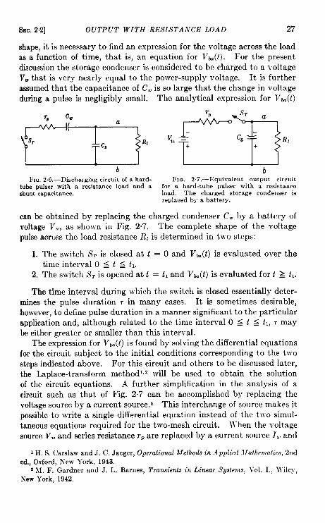
shape, it is necessary to find an expression for the voltage across the loadas a function of time, that is, an equation for V~(f). For the presentdiscussion the storage condenser is considered to be charged to a voltageVWthat is very nearly equal to the power-supply voltage. It is furtherassumed that the capacitance of C. is so large that the change in voltageduring a pulse is negligibly small. The analytical expression for Vk(t)
lc5EIlR‘“m”b b
FIG,26.-Discharging circuitof a hard- FIG. 2.7.—Equivalentoutput circuittubepulserwith a resistanceload and a for a hard-tubepulser with a resistanceehuntcapacitance. load. The charged storage condenseris
replacedby a battery.
can be obtained by replacing the charged condenser Cw by a battery ofvoltage VW, as shown in Fig. 2.7, The complete shape of the voltagepulse across the load resistance R1 is determined in two steps:
1. The switch S, is closed at t = O and Vh(f) is evaluated over thetime interval O S t S tl.
2. The switch ST is opened at t = tl and V&(t) is evaluated for t > tl.
The time interval during which the switch is closed essentially deter-mines the pulse duration T in many cases. It is sometimes desirable,however, to define pulse duration in a manner significant to the particularapplication and, although related to the time interval O s t s tl, 7 maybe either greater or smaller than this interval.
The expression for Vk(t) is found by solving the differential equationsfor the circuit subject to the initial conditions corresponding to the t~~osteps indicated above. For this circuit and others to be discussed later,the Laplace-transf orm method 12 will be used to obtain the solutionof the circuit equations. A further simplification in the analysis of acircuit such as that of Fig. 2.7 can be accomplished by replacing thevoltage source by a current source. 2 This interchange of source makes itpossible to write a single differential equation instead of the t]vo simul-taneous equations required for the two-mesh circuit. IYhen the voltagesource VWand series resistance TPare replaced by a current source Iw and
1H. S. C!arslaw andJ. C. Jaeger,Operational M ethod.s in Applied Mathemat its, 2ndcd., Oxford,N-ewl-ork, 1943.
t hl. F. Gardnerand J. L. Barnes, Transients in Linear Systems, Vol. 1., N-iley,NewYork, 1942.

z
28 THE OUTPUT CIRCUIT OF A HARD-TUBE PULSER [SEC.2.2 ~
shunt conductance gP such that
1.= ~ = v~p,
the circuit shown in Fig. 28 is equivalent to the circuit of Fig. 2“7. Using
+mglb
FIG.2,S.—Equivalentcircuitfor calcu-lating the leading edge and top of thepulsefor a hard-tubepulserwith a resist-ance load, Im = gpV~, gp = I/TP and01 = l/Rt.
Kirchhoff’s current law, the differ-ential equation for this circuit whenthe switch ST is closed is
(9P + 9t)vk + c’s ‘+ = z.. (1)
The Laplace transform of a func-tion V(t) is written V(p), and isdefined by the equation
/v(p) = - V(t)e-@ GY. (2)
o
The Laplace transform for the circuit of Fig. 2.8 is then
(9P + 9Jvbu(P) + cJPvba(P) – Vta(o)l = :1 (3)
in which Vti(0) is the initial voltage on the condenser C, at the beginningof the time interval under consideration. The desired function Vba(t)
is found by solving Eq. (3) for Vk(p) and evaluating the inverse Laplacetransform, thus
Vk(t) = S-qvh(p)].
Let VI(~) OStSt, be the value of V&(t) during the first step in the processof finding the pulse shape for the circuit of Fig. 2.6. Since the condenserC, is assumed to be completely discharged at the instant of closing theswitch, Vk(0) = O. The Laplace transform for Vi(t) is obtained fromEq. (3) by putting Vb(0) = O.
1.
5 (4)VI(P) = c,~ + (g, + 91)-
If the right-hand member of this equation is broken into partial fractions,there is obtained
V,(P) = $ + B
()
g. + glp-t ~
8
(5)

SEC.22] O1:TP1”T U-ITII RESISTANCE LOALI
in which A and B are evaluated by standard methods,
29
giving
A=~=~R,9P + 91
and
B=–~=– $ R,9P + 91
where R, is the effecti~,e resistance of Tpand RI in parallel. The inverseI,aplace transform of V,(p) can then be \vritten
(7)
Equation (6) gives the shape of the leading edge of the voltage pulseacross the load resistance R1. If the sw-itch is closed for a time tl >> R, C,,
the voltage at the top of the pulse is
J/‘8) --ics9, $
The second step in determining the pulse shape ~involves calculating V&(~)~~t,with the switch ST
F]c. 2.9,—Equivalentcircuitforcalculatingthe
open and the condenser G’, charged to the poten- trailingedgeof thepulse
tial difference V](t,) given by Eq. (6). The equiv-for a hard-tubepulse]with a resistanceload.
dent circuit for this step is showm in Fig. 2.9. TheI,aplacr-transform equation for this case is obtained from Eq. (3) bysetting IW = O, gP = O, and Vk(0) = V,(tl) and letting Vb(t)~2~, = V*(t).
Thus
V,(t,)v,(p) = —
P+$’
(9)
from which
V2(Q~~~,= V1(~l)e–02(’–tJ (lo)where
1az = RIC.”
[f ~1>> R, C,, Eq. (8) may be used, and Eq. (10) becomes
(11)

30 TIIE 0[.”TPCT CIRCUIT OF A HARD-TUBE PULSER [SEC.2.2
It is evident from Eqs. (6) and (10) that the stray capacitance acrossthe out put of :Lpulwr-that is, across the load—has an important effecton the times of rise and fall of the pulse voltage. The most efficienthurd-t (llw p~dser is one in ]~hich the load resistance is considerably largerthan the effective resistance of the s]t-itch tube, and hence the timeconstant
U~der such conditions the time for the trailing edge of the pulse to returnto zero, or the initial ~aluc, is greater than that required for the pulsevo(tage to build up to its maximum Yalue. In order to produce as nearlyrectangular a puke as possible ~i-ith a given resistance load, C, must bekept small and r,, should be small.
The effect of the connection to the power supply indicated in Fig. 2.5has been ncglertcd in drawing the equivalent circuits for the pulser out-pllt circuit. Since the isolating element in series ~vith the po~ver supplyusually has an impedance that is high compared \vith r~,,its effect on theleading edge of the pulse is small. For the calculations for the voltageacross the load after the switch is opened, the isolating element is inparallel \rith the 10M1and the shunt capacitance. Thcr~fore, unless theload resistance is also small compared ~rith that of the isolating element,the circuit clement gi in Fig. 29 must be considered as the sum of theconductanees of the load and the isolating element.
From a practical standpoint, it is necessary to have some part of theoutput circuit at ground potential. The cathode of the s\ritch tube isgrounded, since the contribution to C, introduced by the s]ritch tube isbest minimized in this way, and the voltage pulse at the load is thereforenegative. In wxler to obtain a positive pulse at the load, the cathodeof the sivitch tube must be insulated to ~vithstand a high voltage, andconsequently the capacitance of the filament-heating transformer alsocontributes to C,. The presence of C. results in an increase in the averagepower taken from the power supply for a given duty ratio and pulsepower into the load, as is shown in Sec. 2.7.
The effect of the capacitance C, and the conductance gl on the voltagepulse across a resistance load is illustrated in the photographs of oscil-lmcope traces shown in Fig. 2.10. These pictures were obtained with ahard-tube pulscr in ~rhich the capacitance of the storage condenser was0,05 pf, the isolating element R. was 10,000 ohms, r= ]vas approximately150 ohms, and the pulse voltage at the load was 10 kv. oscilloscopetraces of the voltage pulse arc shown for values of C, equal to 50, 80,and 140 ~~f and for Rl equal to 1000, 5000, and 10,000 ohms. Also shownin Fig. 2.10 are the plots of the pulse voltage as a function of time calcu-

SEC.2.2] OUTPUT WITH RESISTANCE LOAD 31
(a) RL = 1000 ohms. (b) R! = 5000 ohms (c) R~ = 10,000 ohms.Capacitancein parallel with the load = 50 ypf.
(d) Rt = 1000 ohms. (e) RI = 5000ohms. (-f) Rt = 10,000 ohms.Capacitance in parallel with the load = 140 ppf.
(o) RL= 1000 ohms. (h) RI = 5000ohms. (i) R! = 10,000ohms.Capacitancein parallelwiththe load = 80 p~f.
(j) Rt = 1000 ohms. (k) R = 5000 ohms. (1) R1 = 10,000 ohms,Pulseshapes calculated from equivalent circuit (m) for shunt capacitance = 80 ~Kf.
ZIlST
FIG.2.10.—Oscilloscopetracesand calculatedshapes
{
~for 10-kv voltage pulses obtained with a bard-tubepulaerfor variousvaluesof load resistanceand shunt 150 10k l?, Cs ‘1capacitance.Sweep speed: 10 div. = 1gsec;verticalscale:10div. = 10 kv.
~b~
(m) Equivalent circuit for cal-culations.

.
32 THE OUTPUT CIRCUIT OF A HARD-TUBE PULSER [SEC.2.3
lated from Eqs. (6) and (10) for the three values of RL with C. = 80 ~pf.Since the 10,000-ohm isolating element is taken into account in thesecalculations, the value of g~ in Fig. 2.9 is the sum (1/R[) + (l/R.).The calculated leading edge of the pulse differs slightly from the experi-mental value in that the observed time of rise is greater than the calcula-tions indicate. This difference occurs because the switch tube does not
II
v— &
(a)
II
__— —— ,,v— ~
(b)~lti. 2.1 I.—Current Voltage characteristic of
a magnetron.
behave as the ideal switch usedfor calculations, principally be-cause of the shape of the driveroutput pulse. The difference is sosmall, however, that the calculatedvalues give a reasonably good pic-ture of the pulse shape to be ex-pected from the pulser.
2.3. The Output Circuit witha Biased-diode Load.—In micro-wave-radar applications, the hard-tube pulser has most commonlybeen used with a magnetron load.The current-voltage characteristicof a magnetron for a particularmagnetic field is shown in Fig.2.11. As indicated in thesesketches, the current through amagnetron is very small until thevoltage has reached the value V,.For most practical purposes the1-V curve can be assumed to havethe form indicated by the dottedline in Fig. 2.1 la, that is, a sharpknee at the voltage V. and zerocurrent below this voltage. Insome cases, however, the behaviorof a magnetron is approximatedbetter by the 1-V characteristic
indicated by the dotted lines of Fig. 2.1 lb. This approximation involvesthe assumption that the magnetron presents a high dynamic resistance tothe circuit for voltages below a critical value V. and a 10}Ydynamic resist-ance above this voltage. Whether the I-V characteristic sketched in Fig.2.1 la or b is to be used in any given case depends on the particular typeof magnetron and the values of the circuit parameters.
For the I-V characteristic of Fig, 2.1 la, the behavior of a magnetronas the load on a pulser is equivalent to that of an ideal diode, that is,

SEC.23] OUTPUT WITH BIASED-DIODE LOAD 33
one that has a linear 1-V characteristic, in series with a battery of voltageV, whose polarity is in opposition to that of the pulse voltage. Forcircuit analysis, it is possible to represent such a load as a biased resistancein series with a switch that is assumed ~P ~to be closed only during the time when a
the magnitude of the pulse voltage is
r:~{
.91
greater than V,.The biased-diode load is used to Z88 5
indicate the effect of nonlinear andunidirectional characteristics of the -?’
load on the output of a hard-tube b
pulser. The output circuit in this case FIG. 2. 12.—Discharging circuit of a
is shown in Fig. 2.12. In this circuithard-tube pulser with a biased-diodeload and a rechargingpath for the
n is the dyn~mic resistance of the storagecondenser.
load, V. is the bias voltage, and St is a switch that is closed only whenVk z V,. The shunt path indicated as Z, must be provided with a
s, s, load of this type in order to allow the chargea
[~>
on the storage condenser to be replenishedafter the pulse.
rp r R.rl
AS Resistame for the Recharging Path .—The
~ Vw = v* simplest form for 2. is a resistance, and thecorresponding equivalent circuit is shown in
b Fig. 2.13. The calculation of the completeFIO.2.13.—Equivalentout-
put circuit for a hard-tube pulse shape for this circuit involves four steps:miserwitha biased-diodeload 1. The switch S, is closed at t = O, St isand a resistance for the re-charging path. The charged
open and Vk(t) is evaluated up to time t= tl,
storage condenser is replaced by such that Vk(tJ = V,.a battery. 2. The switch ST is closed, St is closed att = LI,and Vk(t) is evaluated over the time interval tl s t s tz, where tzis the time at which ST is opened.
3. The switch S. is open, St is closed, and Vb.(t) is evaluated overthe time interval t, s t s t,, where f, is the time at which Vk(t,) = V..
Vk=o
FIG. 2.14.—Sketch of pulse shape indicating the four steps necessary in the calculationsfor a hard-tube pulser with a biased-diode load.
4. Both switches arc open and Vk(t) is evaluated for time t z ts.The procedure is represented in the diagram of Fig. 2.14.

34 THE OUTPUT CIRCUIT OF A HARD-TUBE PULSER [SEC.23
The circuit equivalent to that of Fig. 2.13 with current sources inplace of voltage sources is shown in Fig. 215. In this case Iw = gpV.
FIG. 2.16.—Equivalent circuit for calculating the pulse shape for a hard-tube pulser with abiased-diode load and a resistance for the recharging path.
and 1, = g~V,, where g= = l/rP, g~ = l/rl and g. = l/R,. Using Kirch-hoff’s current law, the equation for this circuit with both switches closedis
(gp+g~+g~)vb.+ C.s% = ~W+~S. (12)
The pulse shape is obtained by solving this equation for Vk(t) using theinitial conditions imposed by the four
m
steps indicated above.c~ g~
Step 1. The equivalent circuit forthis case is shown in Fig. 2.16. Equa-
b tion (12) reduces toFIG. 2.16.—Equivalentcircuit
for Step 1 in the calculation of thepulse shape for a hard-tube pulser (9P + 9Jvba + C*W = 1. (13)with a biased-diodeload.
and the Laplace-transform equation then becomes
(9, + 9S)V1(P) + CJPV1(P) – VI(O)] = ;J (14)
where Vi(p) is the Laplace-transform for Vba(f,) in the time intervalO ~ ~ ~ ~1,fl being the time at which Vba = V,. Since it is assumed that
C, is initially uncharged, V,(0) = O. Solving Eq. (14) for Vi(p),
1.—
V,(P) = ~,p + [, + 98)” (15)
If the right-hand member of Eq. (15) is broken into partial fractions.there is obtained
‘ r(p+&)]”’16Vi(P) = (g, ; g,) ; –

SEC.2.3] OUTPUT WITH BIASED-DIODE LOAD 35
The inverse Laplace transform of this equation is
v,(t) = —%: g, “ - ‘-””)’
(17)
where
al = 9P + 9s.c,
If Eq. (17) is expressed in terms of the parameters of the circuit of Fig.2.13, and the fact that the voltage function is to be evaluated over aspecific time interval is taken into account,
——VI(40SW, = ~ I?I(l – e R,c, t
‘ )’ (18)
where
R,= ~s
Equation (18) gives the voltage at the pulser output as a function oftime up to the time at which the magnitude of the voltage is equal tothat of the load bias voltage V,. At the time t = t1, Vl(tl) = V., theswitch S1is assumed to close, and the starting point for Step 2 is reached.
Step 2. The equivalent circuit during the time interval tl s t s ~~is that of Fig. 2“15 with both switches closed, and the Laplace transformof Eq. (12) is
(9P + 9. + 9JV2(P) + CS[PV2(P) – J“2(~1)l= ~) (19)
where Vz(t) is the value of Vti in the time interval tz — tl, -and ?’~((1) = 1“,is the initial voltage on C, at the start of this inter~’:d. The time (1
is that at which switch ST is to be opened. Solving Eq. (19) for 179(P),there is obtained
where G is written for gP + g, + g~. Equation (20)the form
(20)
may be written in
= (9PVW+ 91VS) 1 _ 1 \ l’, .G ()P
(21)
p+:, P+;

36 THE OUTPUT CIRCUIT OF A HARD-TUBE PULSER [SEC. 23
I’he inverse Laplace transform of Eq. (21) for the time interval underconsideration is
Let R, be the equivalent resistance for rp, R., and rI, in parallel such that
1 A+;+;=G.E= r-p ,
(23)
Then Eq. (22) becomes
~,’’’=~=(2+:)R2°-e-&(t-f’)]+vae’2Equation (24) gives the pulse shape after the voltage has reached thevalue V, and up to the time when switch ST is opened. After some timeL < tz such that
(ta – t,) >> R,C,,
the pulse voltage is very nearly constant, since the exponential termsbecome negligibly small, and Eq. (24) reduces to
‘2(’s)‘($+:)R, (25)
This relation, therefore, gives the voltage at the top of the pulse. Theleading edge and top of the current pulse in the load arc obtained fromEqs. (24) and (25) by calculating the current from the relation
(26)
From this equation it is evident that the current builds up from zero toits maximum value in the time required for the pulse voltage to build up
--#---I’[G. 217.-Equiva-
lent rirruit for Step 3in the calculation of thepuke shape for a bard-tube IJulscr with a biascd-diode load.
from the value V, to I’?(ta), and that this time isless than that required for the voltage to hllild IIpfrom zero to V, if V, is nearly equal to T’,,, l’hctime constant for the current lmil(lllp is R, C..
\J’hen the slritch ST is opened at f = f:, the volt-age across the pulwr output starts to fall, find theshape of the pulse for the next timr interval isfound by the procedure outlined in Step 3.
Step 3. The next calc(llat ion for the ~’oltageVk covers the time t~kcn for the ~wltagr to fallfrom the valIIe T-2(1?)to 1’, again, The c(llli~alcnt
circuit is determined by keeping switch ST open and .S1closed as in[iicate(lin Fig. 2.17. The initial condition for this circuit is that the charge on

SEC.23] OUTPUT WITH BIASED-DIODE LOAD 37
C, must correspond to the voltage V,(t,). Let the value of Vk(t) duringthe calculation be VS(t) and k be the time such that Vi(ts) = V,. TheLaplace-transform equation for this circuit is then
(9, + 9JV3(P) + CJP173(P) – Vz(tz)l = ;“
Solving for V3(p),
Vz(t,)p + g+v,(p) =
4P+9*)
(27)
(28)
In a manner similar to that used in Step 2, the inverse Laplace trans-form of Eq. (28) gives
v3(t)t,9st, = *-~(l–h) _c7.+91
[1–e 1 + V2(t2)e-@l-f*) (29)
Ifg, +gi=+l
v3(t)t,sts1, =-A(t– t,)
$ R? [1 – e ‘“C* ] + v2(@e-&@-”) (30)
At some time k > tz the voltage Va(t) falls to the value V,, at which timethe switch St is assumed to open, The final step in the pulse-shapecalculation is then reached.
Step 4. For this calculation both switches are open, and the initialcharge on C, corresponds to the voltage Vs(ts) = V,. The equivalentcircuit is now reduced to the simple parallel combina- ation of c, and R, as shown in Fig. 2.18.
The voltage Vm = V4(t)tZt, can bemediately,
V4(t)12t, = V,e–&(H, )
written im-
n
c. R,
(31) bF I ~ 2.1S,—
Equivalent circuitThe complete calculation of pulse shape for a cir- for ste~ 4 in the
cuit such as shown in Fig. 2.12 consists of the four calculation of the
steps carried out as above. The composite picture ~~~-~~~~ ~~~ee~of the pulse is obtained by plotting the four voltage with a biaseddiode
functions Vl(t)oStSt,, VZ(t)t,Stst,, V3(t)1,stSt,, andload.
V4(t)t,S, as calculated from Eqs. (18), (24), (30), and (31) respectively,and is of the form shown in Fig. 2“14.
The photographs of oscilloscope traces reproduced in Fig. 2.19a andb show the voltage and current pulses with a magnetron load. Thesetraces were obtained with a hard-tube pulser in which C. = 0.05 pf,Z?, = 10,000 ohms, C, = 115 ~~f, r, = 150 ohms, and the isolatirig ele-
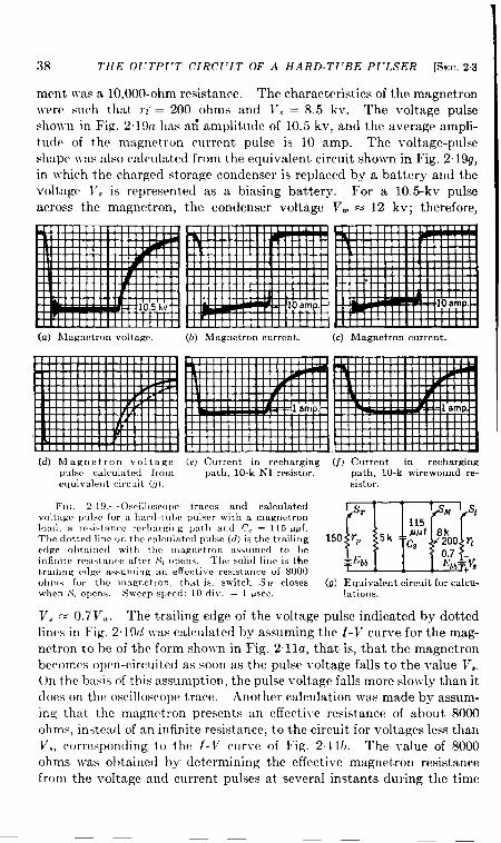
38 IIIE Ol:TP1’T SIRC(’l T
mrnt NYLSa 10,000-ohm resistance.
OF A HA RELT(’BE P1’LSER [f%c. 23
The characteristics of the magnetronwere such that rl = 200 ohms ancf 1’, = 8.5 kv. The voltage pulsesho\vn in Fig. 2 19a has a; amplitude of 10.5 kv, and the average ampli-t udc of the magnetron current pulse is 10 amp. The voltage-pulseshape tvas also calculated from the equivalent circuit shown in Fig. 2. 19g,in which the chnrged storage condenser is replaced by a battery and thevoltage V. is represented as a biasing battery. For a 10.5-kv pulseacross the magnetron, the condenser voltage Vw = 12 kv; therefore,
(a) Llagn.tron voltage. (b) Magnetron current. (c) Magnetron current.
(d) M aR n c t ron volt a g. (e) Current in recharging (-f) Current in rechargingpulse calculated from path, 10-k NI resistor, path, 10-k wirewound re-cquivalent circuit (o1. sister.
FIG. 219. - -Oscilloscope traces and calculatedL.nltxgc pulse for a halcl-tuhr pul.er with a magnetronload, R rwi.tanre recharging path and C’, = 115 ppf.The clotted line on thr calculated pulse (d) is the trailingc’dgc ohtailled with the luw!nctron assumed to beinfinite rcsl~tanrc :iftrr ,St ripen?, The solid line is thetrall]ng V(IXCassun, ing an effcrtive rehihtance of 8000ohms for the )nagnctron, that is, switch ,S.tf closeswhen ,?! opens. Sweep s]]ecd: 10 di~.. = 1 psec.
(u) Equivalentcircuitforcalcu-lations.
V, = 0.7V,.. The trailing edge of the voltage pulse indicated by dottedlines in Fig. 2. l%! was calculated by assuming the I-V curve for the mag-netron to be of the form sho~vn in Fig. 2.1 la, that is, that the magnetronbecomes open-circuited as soon as the pulse voltage falls to the ~’alue V,.(hl the basis of this assumption, the pulse voltage falls more slo}vly than itdoes on the oscilloscope trace. Another calculation was made by assum-ing that the magnetron presents an effective resistance of about 8000ohms, instead of an infinite resistance, to the circuit for voltages less thanV,, corresponding to the 1-V curve of Fig. 21 lb. The value of 8000ohms was obtained by determining the effective magnetron resistancefrom the voltage and current pulses at several instants during the time

SEC.23] OC’TPC’T ll”ITH BIASED-DIODE LOAD 39
the pulse voltage is dropping. The resistance in parallel with C, duringthe fourth step in the calculations for the pulse voltage \vas thereforethat of the 10jOOO-ohm charging path, the 10,000-ohm isolating clement,and the 8000-ohm magnetron resistance in parallel. The pulse shapecalculated under these conditions, sho\rn as a solid line in Fig. 2, 19d,agrees very WCIIwith the oscilloscope trace of 1?g. 2. 19a.
In Fig. 2.19 the traces (e) and (j) were obtained for the current flow-ing in the recharging path during the pulse, .~ noninductive resistorwas used for the trace (e) and an ordinary ~vire-wound resistor for trace(j). The magnetron current pulses corresponding to these t~vo conditionsare shown in Fig, 2. 19b and c where no essential difference is observable.
It is evident from Eqs. (18) and (24) that the effect of R, on the lead-ing edge of the voltage pulse is small, provided that the sn~itch-tuberesistance and the dynamic resistance of the load are small. After theswitch tube and the load have become nonconducting, however, thevalue of R, has a marked effect on the trailing edge of the pulse. Ifthe load is a nonlinear resistance, that is, if there is no bias voltage orswitch S~in the equivalent circuit, the trailing edge of the pulse is deter-mined by the parallel resistance of R. and rl, and as T1increases thiseffective resistance also increases. It is advantageous, therefore, forR, to be as small as possible in order to have the pulse voltage drop quicklyat the end of the pulse. Since R, is in parallel ~vith the load, some pukepower is lost in it, thus increasing the necessary po~ver input to the pulserfor a given load power. From the standpoint of pulser efficiency, it isdesirable to ha~’e as large a value for R, as possible. In choosing a valuefor f?,, a compromise must be made between the need for high efficiencyand that for a steep trailing edge.
Znduc/ante for the Rwharging Path .—The power loss in the shuntelement Z., ~rhich is necessary to provide a recharging path for the storage
I:IG. 221),-Discharging rircuit of a l;IG. 221. -Equi\,alent output circujthard-tube p“lser with a biased-diode load for a hard-tube pulser with a biased-diodennd an inductive path for recharging the load and an inductive path for rechargingstorage condenser. the storage condenser. The charged stor-
age condenser is replaced by a battery.
condenser, can be reduced by using an inductance in place of a resistanceas just discussed. The output circuit of the pulser using an inductancefor Z, is shown in Fig. 2.20 for a biased-diode load. AS before, the charged

40 THE OUTPUT CIRCUIT OF A HARD-TUBE PULSER [SEC.2.3
condenser Cw may be replaced by a battery, and the circuit becomes thatshown in Fig. 2.21. The equivalent circuit for calculating the pulsevoltage as a function of time is again set up by replacing the batteries bycurrent sources, and the circuit of Fig. 2.22, in which the conductanceg, of Fig. 215 is replaced by the series L,R, combination, is obtained.
bFIG. 222.-Equivalent circuit for calculating the pulse shape for a hard-tube pulser with a
biase~diode load and an inductance for the recharging path.
In order to be able to write the Laplace-transform equation for thiscircuit, it is first necessary to find an expression for the Laplace transformof the current in the inductance in terms of V~. Considering this branchfirst,
Vb = L, :1* + R,i,, (32)
for which the Laplace-transform equation is
Vcu.(P) = Ls[Pis(P) – L(O)] + R,i,(P). (33)Solving for G(P),
V~(P) + LA(O).‘i,(p) =
Lap + Rs(34)
The complete Laplace-transform equation for the circuit of Fig. 2.22with both switches closed is, therefore,
(9P + 92) ~ba(P) + c*[Pvk(P) – ~ba(o)l + ‘$y~(”)
= ~, (35)
where Vk (0) and i,(0) are the initial voltage on C, and the initial currentin L, respectively. Solving Eq. (35) for V&(p),
[
i, (o) 1 (Iw + l.)R.V.(o)p’ + v.(o) ; + ~+ – ~ p + ~ L
vba(P) =s S*.
{[ 1(9P + 91)’ ~ + 1 + (g, + gJR.p P’+ :+ ~,
CL. }(36)
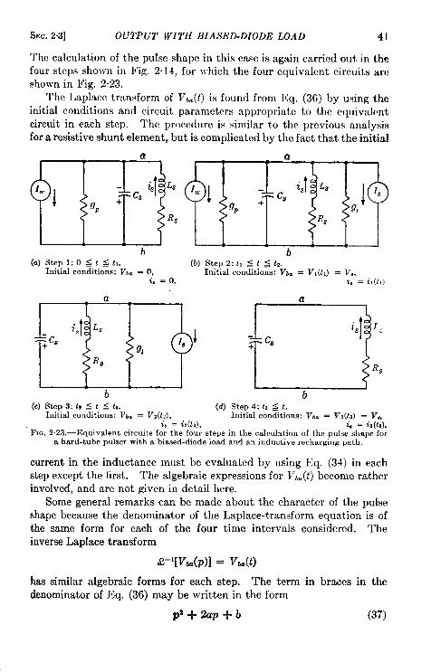
SEC. 2.3] OUTPUT WITI1 BIASED-DIODE WAD 41
The calculation of the pulse shape in this case is again carried out, in thefour steps shown in Fig. 2.14, for ~rhich the four equivalent circuits areshown in Fig. 2.23.
The I,aplace transform of V~a(t) is found from Eq. (36) by using theinitial conditions and circuit paramctws appropriate to the equivakmtcircuit in each step. The procedllre is similar to the previous analysisfor a resistive shunt element, but is complicated by the fact that the initial
a
m bi - ‘; ‘h :
a
l,,I
t4 Ls lx!
~ isf L, ,+ Cs
is
9r 9P + s 9,R$ R8
h b(a) step 1:0 s tst,. (b) Step 2: t, S t ~ t,.
Initial conditions: Vba = O, Initialconditions:Vb. = V, (t,) = }’,,i, = o.
Step 4: tj s t.Initial conditions: Vb. = V.a(h) = V,.
(c) Step 3: i, s t S h. (d)Initialconditions:~b~= V2(t?),
z, = i*(t2). .,, -t, = is(h).FIG.2.23.—Equivalent circuits for the four steps in the calculation of the pulse shape for
a hard-tube pulser with a biased-diode load and an inductive recharging path.
current in the inductance must be evaluated by using Eq. (34) in eachstep except the first. The algebraic expressions for V*.(L) become ratherinvolved, and are not given in detail here.
Some general remarks can be made about the character of the pulseshape because the denominator of the Laplace-transform equation is ofthe same form for each of the four time intervals considered. Theinverse Laplace transform
J3-’[vti(p)] = Vk(t)
has similar algebraic forms for each step. The term in braces in thedenominator of Eq. (36) may be written in the form
p~+2aP+b (37)

42 THE OUTPUT CIRCUIT OF A HARD-TUBE PULSER [SEC.2.3
where
[ 12(2= :+(’”:”) ,. *
and
(38)
(39)
This term may be put in a form more convenient for finding $-l[vb(P) ]by completing the square, thus
p2+2ap+b=(p+a)2+u2
where~Z=b—aQ.
The right-hand member of the Laplace-transformbroken up into partial fractions with the result
B,(P + a) + BZK.@=++ (P+ U)2+U2’
(40)
(41)
equation can be
(42)
where the terms A, Bl, and B, are evaluated by standard methods. Theform of the inverse Laplace transform now depends on the following threeconditions that can be placed on U2:
1. If b > a’, W2 > 0.2. If b = az, # = (),
)
(43)3. If b < az, cd < 0.
Condition 1. U2 >0. The inverse Laplace transform for Eq. (42)is
V~(t) = A + Ble-a’ cos d + ~ e–”’ sin cot. (44)
Condition 2. u’ = O. The inverse Laplace transform for Eq. (42)is
V&(t) = A + B,e-ot + Bale-a’. (45)
Condition 3. W2<0. Let U2 = – IC2, then the inverse Laplacetransform for Eq. (42) is
Vk(t) = A + B,e- cosh kt + ~ e-’ sinh id. (46)
The Eqs. (44), (45), and (46) are of particular interest in connectionwith the calculation of the trailing edge of the pulse, that is, in Step 4of Fig. 2.14. In this case the expressions for U*and kz are
1 R’—J .‘2 = C,L, 4L:
(47)

●
SEC.2.3] OUTPUT WITH BIASE~DIODE IJJAD 43
and
The trailing edge of
and is aperiodic if
the pulse is part of a damped oscillation if
(48)
449)
(50)
If condition (49) exists, the voltage across the pulser output oscil-lates at a frequency determined by Eq. (47) after the switch tube and theload become nonconducting. The voltage therefore passes through zeroand reverses its polarity. This reverse voltage appearing at the pukroutput is commonly referred to as the “backswing voltage.” The periodof the oscillation becomes smaller as R, is decreased, and the traiLing edgeof the pulse becomes steeper as the ratio R./L. is decreased relative to2/dCaL,. The damping of the oscillation depends on the exponentialterms in Eq. (44) and, since the exponent is R,/2L,, a lower value forR,/L, causes a decrease in damping and hence a higher value for the back-swing voltage. A high backswing voltage is very undesirable because itadds to the power-supply voltage at the plate of the switch tube, andincreases the danger of flash-over and sparking within the tube.
The magnitude of the current that builds up in the inductance alsohas an effect on the rate at which the voltage drops at the end of the pulse,aa is evident if the coefficients A, B1, and B: are evaluated for the equiva-lent circuit of Step 4. From Eqs. (42) and (36) these values become
A=O,
B, = V,(t,) = V,,
and
B,=~-a~.* # I (51)
When Bs is negative, that is,
i3(t3) > V,R,——C. 2L, ‘
it is seen from Eq. (44) that, as is(ts) increases, the value of V4(t) decreasesmore rapidly for given values of the other parameters. The value ofiJtJ increases with time up to a limiting value determined by the mag-nitude of R,. As long as the current in the inductance continues toincrease with time, therefore, the trailing edge of the pulse is steeper for

.
44 TIfE OUTPUT CIRCIJIT OF A IIARD-T1,’RII PCI.,YER [SEC.23
the longer puke durations than for the shorter ones. ‘~hc oscilloscopetraces shown in Fig. 2.25 illustrate this lmhavior.
The oscillating voltage at the cncf of the pulw is undesirable not onlybecause it produces backswing vf)ltugc, but also Imcausc it bmomcs ofthesame polarity asthcfor\v:ir[l p\llsevoltagc{ )nthcr(,il lrns\wing, T}iispost-pulse voltage may be large enough to cause apprecia})le current toflow in the load, andthcrcforc isaseconrla rypulsc. JV}lenthcdampirrgintroduced by the resistance of the inductance is small, it is necessary toincrease the damping by connecting a cliodc across the pulser output insuch a way that it is conducting only ~vhcn there is backsiving voltage.The equivalent circuit ~vith a shunt dioclc is sho,rn in Fig. 2.24. The
La
R,
bFIG.224.-Equivalent circuit fur calculating the pulse >hapc for a hard.tube pul~er
with a biased-diode load, an inductive recharging path, and a shunt diode to reduce tl, c“ backswing voltage.”
diode is represented by the conductance g~and switch & that is assumedto close only when the voltage Vk is opposite in sign to the normal pulsevoltage. If gd is large, the backswing voltage is negligibly small, and nopost-pulse voltage appears with the same polarity as the pulse voltage.
The oscillating voltage after the pulse can also be avoided by makingR,/L, > 2/-. For this purpose, an inductance with high resistance,that is, an inductive resistor, must be used and, under such conditions,the voltage corresponding to the trailing edge of the pulse becomesaperiodic, as shown by Eq. (46). The time of fall for the voltage dccrcasesfor smaller values of the ratio R,/L,, and the transition bet~vcen theaperiodic and oscillating condition occurs when this ratio equals 2/m.From a practical standpoint, such an inductive resistor is usually designedto have a ratio of R,/L, slightly less than the minimum for the aperiodiccondition. For this condkion, the voltage is oscillatory, but the dampingis high and the backswing voltage is correspondingly small. The choicebetween a large value of R,/L, without a shunt diode or a small \,alue ofR,/L, with a shunt diode depends on the importance of having a smalltime of fall for the voltage pulse.
It is difficult to make a detailed analysis of the effect of the circuitparameters on the leading edge of the voltage pulse \vithout actuallycarrying out the calculations for V~.(t) using numerical values for the

SEC. 2.3] OUTPUT WITH BIASED-DIODE LOAD 45
circuit components. A very general statement can be made, however,to the effect that, as the switch-tube resistance or the shunt capacitanceincreases, the time of rise for the voltage pulse also increases. Theeffect of the shunt inductance on the leading edge of the pulse over afairly wide range of values for the ratio R./L. is rather small.
If there is a resistance in parallel with the shunt inductance, the timesof rise and fall of the voltage pulse become shorter: the smaller the resist-ance, the smaller the rise and fall times. Such a resistance is introducedinto the circuit when the connection to a power supply for recharging thestorage condenser, as indicated in Fig. 2.5, is considered. In Sec. 2.4 it isshown that for good pulser design, the resistance R. is large, but its effecton the trailing edge of the pulse is still appreciable.
A set of photographs of oscilloscope traces illustrating the effects ofvarious circuit parameters, together with the pulse shapes calculatedfrom the equivalent circuits discussed above, are shown in Figs. 2.25,2.26,2.27, and 2.28.
The oscillosco~e traces reproduced in Fig. 2.25 were obtained withthe magnetron and pulser used for the pictur~s of Fig. 2.19, replacing theresistance recharging path in the pulser by a lknh inductance and ashunt diode. In each case the magnetron voltage and current pulsesand the current flowing in the 10-mh inductance are shown for pulsedurations of 0.5, 1, and 2 psec. The pulse voltage and pulse current wereadjusted to 10 kv and 10 amp respectively for each pulse duration. Theeffect of the increase in current in the shunt inductance is shown in themore rapid fall of voltage as the pulse duration increases. The calculatedvalues for the voltage pulses (j), (k), and (1) take into account the 10,000-ohm isolating resistance and an assumed equivalent resistance of 8000ohms for the magnetron after the voltage has dropped to the value V..
The oscilloscope traces shown in Fig. 2“26 are for the l-psec pulseduration with a sweep speed about one tenth of that used for the tracesof Fig. 2.25. The traces (a), (d), and (g) are the slow-sweep presentationof the l-psec pulses shown in Fig. 2“25, and indicate the effect of a goodshunt diode, that is, one with high cathode emission. The traces (b),(e), and (h) were obtained with a shunt diode having lower cathodeemission, and a small backswing voltage of about 1 kv is observable onthe voltage pulse. The traces (d), (e), (g), and (h) show that the cur-rents in the lo-mh inductance and in the shunt diode decrease morerapidly when the shunt diode has a higher effective resistance. Whenthe shunt diode is removed from the circuit, a backswing voltage of about6 kv appears after the voltage pulse, and the pulse shapes of Fig. 2“26cand f are obtained. The oscillation resulting from the use of the induct-ance for the recharging path is damped by the 10,000-ohm resistance ofthe isolating element that is in parallel with the discharging circuit for
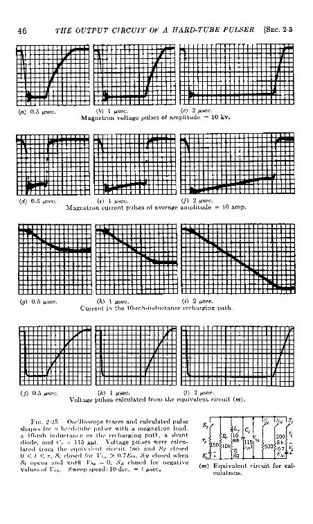
46 THE OUTPUT CIRCUIT OF A HARD-TUBE PULSER [SEC. 23
(a) 0.5 psec. (b) 1 #sCC. (c) 2 psec.Magnctuon voltage pulses of amplitude = 10 kv
(d) 0.5 #sCc. (e) 1 /AsCc, (f) 2 psec.Magnetron current pulses of ax,crage amplitude = 10 amp.
(0) 0.5 WCC.curl
(j) 0,5 WCC.voltage
(h) 1 ~se.. (i) ? psec..ent in the 10-mh-inductance rcrhar~ir]z path.
(k) 1 Ksec. (/) 2 #sec.pulses calculated from the cquiwdent circuit (m).
l:r~. ?25.-Osrilloscopc traces and calculated pulseshnlws for :1 IB:trd-tl]lw plllw-r with a magnetron load,:L 10-mh indurt:tllce m tltr mrharging path, a shunt,Iimlc, :Ll,d (’, = I 15 w(. I“oltage pulses mere cxlru-l:ltwl (,oln tllr rqllix-:llcnt circuit (m) aud ,S7 clrwcclO < t< r.,SI?lOs(-(1f<,r 1’!,,, > 0.7 E1,1,,SM closedwhen,sI Ol,c,is :~u,]u!itil 1-,,. = O, .~~closed for neg:ltiveValuesof 1-,,., Sweepspeed:10 div. = 1 psec.
~[
.sd .5, .$ST L, C,
~ 10 200 ~G mh ~~5vb.
150 lok 8k ./!f 500 0, ~
~b: ;20 h = 4
(m) Equivalent circuit for cal-culations.

SEC. 2.3] OUTPUT WITH BIASED-DIODE LOAD 47
the shunt capacitance. The calculated values for the current in the10-mh inductance are plotted in Fig. 2.26i, assuming the effectiveresistance of the shunt diode to be 500 ohms. It can be seen that thecalculated current in the inductance for the l-psec pulse agrees very wellwith the corresponding trace obtained when the good diode was used.
(u) GoOd >huut diode. (b) Poor shunt diode. (c) No shunt diode.hlagnetron voltage pulses.
(d] Good shunt diode. (e) Poor shunt diode. (J) No shunt diode.Current in the 10-mh-inductance recharging path.
(!21@J~dshuut diode. (h) Poor shunt diode. (i) Calculated currents in theCurrent in tllc shunt diode. recharging path for the
circuit (m) of Fig. 2.25.I;l(:. 226.-0scilloscopc traces a],d calculated ~~~h~rgi~g-p~th~Urrent~for ~ h~rd-t~be
pulscr with a Inaguctroli load and a 10-mh inductance as the recharging path. (a) and (d)arc tile Jow-sweep-speed presentations corresponding to the l-psec pulses of Fig. 2.25.Hurizor,tal scale = 1 pser/di\..
\\-hen an inductive resistor ~vith a resistance of 7500 ohms and aninductance of 3 mh is used for the recharging path in the pulser, the oscil-loscope traces appear as show-n in Fig. 2.27. The small backswing volt-age that appears after the pulse indicates that the value of R./L. for thisinductive resistor is slightly less than the value for critical damping.The magnitude of this backswing voltage is so small, however, that a

(a) 0.5 psec. (b) 1 #sec. (c) 2 psec. (d) Voltage pulses calculated from
Magnetron voltage pulses of amplitude = 10 kv.
(e) 0.5 psec. (j) 1 psec. (Q) 2 psec.
Magnetron current pulses of average amplitude = 10 amp
equivalcut circuit (h).
(h) Equivalent circuit for calcu.lations.
(i) 0.5@e.. (j) 1 psec. (k) 2 LILWC. (J) Currents in the recharging pathCurrent in the 7600-ohn3-mhrechargingpath. calculatedfrom the equivalentcir-
cuit (h).FIC+.2,27.—Oscilloscopetracesandcalculatedpulseshapesfor a hard-tubepulserwitha magnetronload, a rechargingpath consistingof a
7W0-ohmresistance in wriea with a 3-mh inductanc~, and shunt capacitance of 115 ppf. In the calculations the effective resistance of themagnetron was assumed to be 8000 ohm. after .S, oPens. th=t i., SM C1OS..when S, opens. Sweep .peod : 10 div. - 1 ~s.ac.

SEC. 23] 0[’TP(’T li”l TH BIASED-DIODE LOAD 49
shunt diode is unnecessary. From a comparison of the voltage pulsesof Fig. 2.27 with those of Fig. 2.25 it is seen that the voltage for the 0.5-psec pulse drops at alm~[t the same rate in each case. .\t a pulse durationof 2 ~sec, the voltage drops faster \\-iththe 10-mh inductance for the
(0) 1)1*c = 10div. (b) 1P wc = 1 div. (c) Calculatedfor circuit~.Magnetronvoltagepulsesof amplitude= 10 kv.
(d) lU sec = 10 div. (e) 1P sec = 1 div. U) Equivalent circuit for calculations.Magnetron current pulses of average amplitude = 10 amp.
@) 1P sec = 10 div. (h) 1P sec = 1 div. (i) Calculated from circuit (-f).Current in the X)-mh inductanrc rechargi!,g path,
FIG. 228.- Oscilloscope traces and calculated pulse shalms for a }I:ird-tube pulser witha magnet r-on load, a 20-mh inductance as the iholatittg clertlet, t, a X-1X,1, illduvta]lw as therecharging Path, ]Lo ~llu!it diode, :it]d (’. = 115Pfif, ~lJ[t;Lg(> ])UIX! >L!l<l rllr,c!)t ill the
20-mh uxha,g]r,g ],ath calculated frc,m cquivale!,t circuit (J) witl, tl~e r<,,,ditioa,s: ,s~ opensat fz, St opens at t,, S.v, closed fj to t<, all switches open t, to /s, S.11,rlosed (J to /6, all switchesopen 16to 17.
recharging path than with the 3-mh 7500-ohm ind~lctive resistor. Thereason for this behavior is evident from a comparison of the currents inthe recharging paths.
For the oscilloscope traces of Figs, 2.25, 2.26, and 2.27 the isolatingelement was a 10,000-ohm resistance. If an inductance having a low

50 THE OUTPUT CIRCUIT OF A HARD-TUBE PULSER [SEC. 2.3
resistance is used for this isolating element, the damping of the oscillationthat occurs after the switch tube becomes nonconducting is usuallysmall, as shown by the pictures reproduced in Fig. 2.28. These pic-tures were obtained with the magnetron load, an inductance of 20 mhas the recharging path, and an identical inductance as the isolatingelement. Each of these inductances had a resistance of 160 ohms. Thebackswing voltage for this circuit becomes larger than the pulse voltagewhen there is no shunt diode, as can be seen in Fig. 2.28b. Since thedamping in the circuit is small, the voltage swings back to the polarityof the main pulse and causes a small current to flow in the magnetron,as indicated by the trace (e). In calculating the voltage across the loadas a function of time from the equivalent circuit shown in Fig. 2.28f, itis therefore necessary to introduce an effective resistance for the magn~tron during the time when this post-pulse conduction occurs. Thecalculated values plotted in Fig. 2.28c and i were obtained by assumingthe effective resistance of the magnetron to be 8000 ohms, and the magni-tude of the voltage for the trailing edge of the voltage pulse was con-sidered to be less than V, but greater than zero. During the timecorresponding to the backswing voltage, the magnetron is considered tobe open-circuited, and hence to have an infinite resistance. When thepost-pulse conduction occurs, the magnetron is assumed to appearas a lo,000-ohm resistance. The comparison of the plots for the loadvoltage and the current in the recharging path with the correspondingoscilloscope traces indicates good agreement between calculated andexperimental values.
The assumptions made in the foregoing calculations with regard tothe effect of the magnetron on the behavior of the pulser output circuitlead to reasonable agreement with the experimental data. This agree-ment may be considered a justification for the assumption that the shapeof the 1-V curve for a magnetron, shown in Fig. 2“1lb, can be C1OSCIYapproximated by a high dynamic resistance for voltages less than V,,and by a low dynamic resistance for voltages greater than V,. If theload resistance is nonlinear, the functional relationship between n andVk must be taken into account in the calculations, and the analysis ofpulse shape becomes considerably more complicated. Another com-plication arises if it is necessary to consider the variation of switch-tuberesistance with the plate current in the tube.
At the start of this discussion of pulse shape as affected by pulsercircuit parameters, it was assumed that the capacitance of the storagecondenser was very large in order that the voltage across it could beconsidered constant during the pulse. It is stated in Sec. 2.1, however,that the storage-condenser voltage is less at the end than at the beginningof a pulse. This change in voltage depends on the magnitudes of the

SEC.2.3] OUTPUT WITH BIASED-DIODE LOAD 51
puke current, the storage capacitance, and the pulse duration. As isshown in the following section, it is often impractical to have a storagecapacitance that is large enough to keep this voltage change less than afew per cent of the initial condenser voltage. The actual pulse shapeobtained from a hard-tube pulserof this type, therefore, does nothave a flat top, but rather has a –sloping top as indicated in thesketch of Fig. 2.29.
Since with a resistance load gthe pulse current has the same vmaxshape as the pulse voltage, the FIG. 2.29.—Sketch of the voltage pulse
shape showing the effect of the drop inratio AZ/1-, is equal to the ratioAVIV-,. If the load is a biased-
storage-condenser voltage during the pulse.
diode or magnetron with a low dynamic resistance, however, the ratioAI/Iw may be many times as great as the voltage ratio AV/V_. InSec. 24 it is shown that
Al _ AV . V...I vu= Vmax– v.”ma.
The effect of the drop in pulse voltage on the current in a load that has alow dynamic resistance can be seen in the oscilloscope traces shown inFigs. 2.19, 225, and 227. It is also evident that, if AV is large, it ispossible for the pulse voltage to fall below V. before the switch ST isopened. As a result, the load current stops flowing before the end ofthe intended pulse interval.
If the switch-tube resistance increases with time during the conduc-tion interval, the effect is similar to a change in voltage on the storagecondenser. Such behavior of the switch tube is experienced with someoxide-cathode tubes, particularly for long pulses and high currents, andis referredto as cathode fatigue. It is very difficult. to take into accounttheeffect of cathode fatigue on the pulse shape, since it can vary so muchfrom one tube to another of the same type. The magnitude of thecathode fatigue tends to increase as the tube gets older, but it is notuacommon for it to decrease during the first few hours of operation.
THE CHARGING OF THE STORAGE CONDENSER
The energy removed from the storage condenser during the pulseinterval causes the potential difference across this condenser to be less8t the end than at the beginning of the pulse. If the output of the pulseris to be a succession of identical pulses, it is necessary to provide somemeans by which the energy in the condenser can be replenished duringthe interpulse interval. This energy can be supplied by connecting the
[=J’ ,
E. G. & G. LIBRARY ,-” +.,. ,,,.,
LAS VEGAS BRANCH ,;,:’l -~.,

52 THE OUTPUT CIRCUIT OF A HARD-TUBE Pi7LSER [SEC. 2.4
condenser to a primary electrical-energy source such as a battery or powersupply during the interpulse interval. The ideal arrangement would beto make the charging and discharging cycles completely independent byusing a switch as shown in Fig. 2. la. The use of such a switch is imprac-tical for pulses that recur at rates of several hundred to several thousandper second. The pulser must therefore be designed with a conductingpath between the condenser and the power supply that has the leastpossible effect on the discharging of the condenser during the pulseinterval.
One method that is used to isolate the power supply from the con-denser-discharging circuit is shown in Fig. 2.5. In this method a resist-ance element is connected in series with the power supply. If thisresistance is sufficiently high, the current that flows through the switchtube from the power supply is small enough to be neglected. Whenthe switch tube is conducting for a very short time interval—that is, forshort pulse durations—an inductance in series with the power supply canprovide satisfactory isolation. This method has the disadvantage thatthe current from the power supply increases \\-ithtime and, since thiscurrent flows through the switch tube, the tube drop during the pulse isalso a function of time.
Although the reason for introducing the isolating element is to keepthe current flow-ing from the power supply through the switch tube assmall as possible, there are other points to be considered in choosing theparticular element. Since the condenser is connected to the powersupply in order to be recharged, the isolating element must not make thecharging time constant so large that the condenser voltage at the end ofthe interpulse interval differs appreciably from the power-supply voltage.The connection to the power supply during the pulse interval has aneffect on the leading edge and on the top of the pulse. The magnitudeof this effect depends on the relative size of the impedances of the isolat-ing element, the switch tube, and the load. When the switch is non-conducting, this isolating element is effectively in parallel with the pulseroutput circuit and therefore has an effect on the trailing edge of the pulse.These effects on the pulse shape can be taken into account in the analysisof the discharging circuit, as discussed in Sees. 2“2 and 2.3, by introducingthe isolating element as an additional circuit parameter. The ultimatechoice of the element is generally based on a compromise between theseconsiderations.
2.4. The Output Circuit with a High Resistance as the IsolatingElement.—The equivalent circuits for the pulser with a high resistanceas the isolating element are shown in Fig. 2.30a and b. For reasonsalready stated, the resistance R. is assumed to be very large comparedwith r,. The analysis of the circuit behavior during the interpulse

8EC.%4] A HIGH RESISTANCE AS THE ISOLATING ELEMENT 53
interval (that is, when switches ~= and & are open), is similar for thetwo circuits (a) and (b) if Z, is a resistance. If Z, is an inductance, thealgebraic expressions become complicated, and circuit (a) is thereforeused as the basis for the present discussion.
TP c.
m
S* RC RI
z EM
(a) Resistance load.Fm. 2,30.—Hard-tube pulser circuits
with
(b) Biased-diode load,with a resistance as the isolating element in seriesthe power supply.
Assume that the switch AS, is open initially for a long time andtherefore that the condenser C~ is charged to the voltage of the powersupply, If the switch is then closed for a time 7 and open for a timeT, – ~, and this procedure is repeated, a succession of pulses is obtainedwith a recurrence frequency .f, = I/ T,. During the time , the con-denser voltage decreases and during the time T, – T it increases. If thetime 1’, – r is not many times greater than the time constant of thecircuit, the condenser voltage is appreciably less than the power-supplyvoltage at the end of this inter~-al, Equilibrium values for the condenservoltage at the beginning and at the end of the interval 7 will be obtainedif the switching procedure is repeated a sufficiently large number of times.This approach to equilibrium is shown diagrammatically in Fig. 231.
Ebbk 74--~r7 47-L-Tr-~+74——+————————~——b————————i——T———-
—___ —-___—1
FIG, 2.31 .—The x.oltagc on the storage condenser of a hard-tube pulser as a functionof time after the start of a series of regularly spaced puke, when a resistance Isolating ele-ment is used.
It is of interest to obtain the value of Vu ,’EM for any given set ofcircuit parameters. Let l’;, be the value for the condenser voltage atthe start and V; be the voltage at the end of any particular pulse,and let V,, and 1’, be the equilibrium values of these voltages. Duringa charging interval the switch ST is open, and the expression for thecondenser voltage as a function of time is
(52)

54 THE OUTPUT CIRCUIT OF A HARD-TUBE PULSER [SEC. 24
\vhere t is measured from the start of the interpulse interval. Thecondenser voltage at the end of the interval is then
(53)
If it is assumed that R.>> r,, the connection to the power supply maybeneglected ~vhen considering a discharging (pulse) interval. The con-denser voltage during this interval is thus
(54)
where t’ is measured from the start of the discharging interval. Thecondenser voltage at the end of this interval is then
For a continuous succession of pulses the equilibrium values of V; in
f?qs. (53) and (55) must be equal and likewise the values of V;. Solvingthese equations for V;, there is obtained
(56)
which may be writtenVu = EMy. (57)
A similar solution for V: gives
From Eq. (56) it is seen that the value of the ratio Vw/Ew for a givenset of circuit parameters increases as 7 is decreased and T, is increased.Also, for given values of r and T,, the condenser voltage approaches thepower-supply voltage as R. and C. are decreased. By decreasing R,,
however, the current through the switch tube is increased. This increaseis particularly undesirable in high-power pulsers where the load currentand hence the switch-tube current are already large. The effect of vari-ations in T, T, and CWare illustrated in curves of Fig. 2.32. These curveswere calculated from the exact expression for the equilibrium condenservoltage V., taking into account the effect of the power-supply connectionon the discharging circuit. The equation for Vw is
‘.=2$%-(1+%’) (59)
Sm
.241
AH
IGH
RE
SIS
TA
NC
EA
ST
HE
ISO
LA
TIN
GE
LE
ME
NT
55
Wz
7i-A
w,J
WZ
TA

56 THE O(lTP1:T CIRC(”IT OF A I{ AR D- T1:BE P(JI,SER [SEX-.24
and the voltage at the end of the pulse becomes
If R. >> rP,
(60)
(61)
1a = (i-p + R,)cu’ (62)
and # = -f. Thus, for R. = 100rp, the value of V,, calculated from Eq.(59) is about 1 per cent greater than the approximate value calculatedfrom Eq. (56). In designing many pulsers, it is therefore sufficientlyprecise to calculate the equilibrium condenser voltage by neglecting theeffect of the polver-supply connection on the discharging circuit.
If only the charging circuit for the storage condenser is considered,an advantage is apparently gained by having the capacitance as smallas possible. This supposition is contrary, however, to the conclusionreached by considering the discharging circuit. From Eqs. (59) and(60) the difference in the condenser voltage at the beginning and at theend of a pulse is
[ 1V,,l – v, = Vw “7’(1– c;”’)rp + Rt-y
(63)
Equation (63)from Eqs. (57)
may be reduced to the corresponding relation obtainedand (58) if R, >> r,, namely
v,,. – v. = 1’,,[1– c-(’r+~’w (64)
If 7<< (i-, + R~)C’t,, Eq. (64) may be written
v,,, – v, = VWT(r= + R1)C,.
(65)
Again, if V,,. – V. is small, the change in load current during the pulseis small and
V,(.11=—
r= + R’

i%C. 2.4] A HIGH RESISTANCE AS THE ISOLATING ELEMENT 57
\rhichleads to the approximation
This expression may be used to determine the magnitude of the capaci-tance required for a particular load current in order to keep the loadvoltage \vithin certain limits during the pulse. In general, it is desiredthat the load voltage during the pulse be as nearly constant as possible,and therefore C,. must be large.
The same conclusion is reached if a corresponding analysis is madefor a biased-diode load in the circuit of Fig. 2.3(W. If it is assumed thatthe potrer--supply connection may be neglected in [Determining the con-denser voltage during the pulse inter~wl, the difference in condenservoltage at the l)eginning and at the end of the p~llsc is
v,, – t’. = (v,. – V*) [1 – c “’.+’’)r’——
‘ 1. (67)
The relation (66) is obtained from Eq. (67) I),v the same reasoning usedto obtain it from Ill. (64) using the approximation that
is may be seen from a consideration of the change in load currentduring a pulse, it is more important to keep the change in load voltagesmall for a biased-diode load than for a resistance load. >“eglecting thepower-supply connection again, the currents at the beginning and atthe end of a pulse for a resistance load are,
and
For the biased-diode load, the corresponding currents are
and
(1;), =v,,. – v.
TP + TL
l’, – l“”(1;), = —
r,; + f’1 “ I
(68)
(69)
The ratio of the change in mlrrent (Illring tlic lnllsc tu the cllrrrnt at the

58 THE OUTPUT CIRCUIT OF A HARD-TUBE PULSER [%C. 2.4
beginning of the pulse for the resistance load is therefore
(1,)0 – (11), = vu); v,,(11)0 W
(70)
and for the biased-diode load,
(1;)0 – (1;)7 _ VW – v,.(1;), – v. – v. (71)
It is evident from Eqs. (70) and (71)
0.4
0.3
QL(It )0
0.2
0.1—
.o.1~ seco0,01 0.02 0
CapacitanceCwinAfFIG.2.33.—Ratioof the changein load
currentduringa pulseto the load currentat the startof the puke for variousvaluegof pulsedurationand storagecapacitance.This ratio is approximatelyequal to theratio of the changein condenservoltageduringthe pulseto thevoltageat thestartof the pulse. The curves are plotted forR = 1000 ohms, R. = 10,000 ohms, and7P = 100 ohmg.
that, for a given percentage changein load current, the ratio of thevalue of Vu — V, for a biased-diodeload to that for a resistance load is
v. – v.Vw “
The effect of the capacitance ofthe storage condenser on the currentthrough the load during a pulse isillustrated by the curves of Fig.2.33. These curves are plottedfrom the equation
(Zl), – (Z1), = (1 – ~-~,), (72)
(11)0
where a is the value given by Eqs.(61). From Eqs. (64) and (70) asimilar expression is obtained inwhich a = 1/ (TP+ IL) C., namely,
(IJO – Ul)r = [~ _ ~ (r,+k)cw]_—
(11)0=Vw–v,
v.. (73)
Curves of the type shown in Figs.2.32 and 2.33 can be used to deter-mine the best value for the capaci-tance of the storage condenser for
given values of r and T, when R, >> rp. A compromise must be made
between the equilibrium condenser voltage and the amount of voltage dropthat can bet olerated during the pulse for the particular pulser application.
From Eqs. (52) and (54) it is possible to calculate the time requiredfor the condenser voltage to attain a value approaching VW after thebeginning of a succession of pulses. This time can best be expressed in

SEC. 2.4] A HIGH RESISTANCE AS THE ISOLATING ELEMENT 59
terms of the number of pulses such that (V~)m = kVw, with k some valueslightly greater than one. The curves plotted in Fig. 2.34a and b give
the values of n as a function of the capacitance of the storage condenserfor k = 1.01 and 1.001 and for several values of 7 and T,. If the valueVJEM is much less than 1.0, the number of pulses required to approachthe equilibrium value may affect the operation of loads with low dynamic
.
—
—
1
—
—
7//&
o!
—
—
/
40
30
j.:20;
2
0.060.0s0.1 02 0.4CapacitanceC. inti
[d
10
a1 0.02 0.040.060.0s1
C.3pwitmceC. i
[b)
02 0.4
I?m.244.—Numberof pulsesrequiredfor thestorage-condenservoltageto reachkVwasa functionof Cuforvariousvaluesof r andT,, withR. = 10,000 ohms, Rt = 1000 ohms,andrp = 100ohms,(a) k = 1.01, (b) k = 1.001.
impedance such as the magnetron. A large value of n indicates that thecurrent through the load is larger than the current obtained with con-tinuous pulsing for a time that may be long enough to be deleterious tothe magnetron cathode. This high current may also aggravate anytendency for sparking to occur in the load.
In designing a hard-tube pulser with a resistance as the isolatingelement, it is important to know how much average power will be dis-sipated in the resistor. There are two major contributions to this power,that from the current flowing in the resistance during the pulse intervaland that from the current flowing during the interpulse interval. Whenthe switch tube is conducting, the current flowing in the isolating resist-
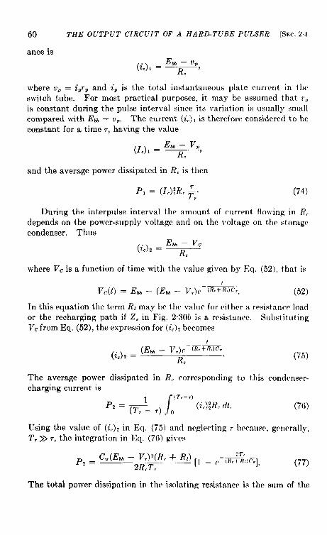
60 THE OUTPUT CIRCUIT OF A HARD-TUBE PULSER [SEC. 24
ante isEM – VP
(i.) , = —R~)
where v= = iprP and iP is the total instantaneous plate current in theswitch tube. For most practical purposes, it may be assumed that t’,is constant during the pulse interval since its variation is usually smallcompared with 11~~– u=. The current (i.), is therefore considered to beconstant for a time ~, having the value
Ew – VP(I.), = ~–,
c
and the average power dissipated in R. is then
During the interpulse interval the amount of current flowing in R,
depends on the power-supply voltage and on the voltage on the storagecondenser. Thus
EM – Vc(i,), = ~
c
where Vc is a function of time with the value given by Eq. (52), that is
In this equation the term R[ may be the ~.alue for either a resistance loador the recharging path if Z, in Fig. 2.30b is a resistance, SubstitutingVc from Eq. (52), the expression for (i.), becomes
(75)
The average power dissipated in R, corresponding to this condenser-charging current is
1
1
(T,–,)
“=( T,-7) “(i.);R, dt. (76)
Using the value of (i,), in Eq. (75) and neglecting r because, generally,T, >> T, the integration in Eq. (76) gives
p, = C,,.(EW – V,)’(R, + R,) [l _ c-&Rml2RcTr
“. (77)
The total power dissipation in the isolating resist~nce is the sum of the

SEC. 25] AA’ I,VDUCTAXCE AS THE ISOLA TI,VG ELEAf EXT 61
values for the pulse interval and that for the interpulse interval givenby Eqs. (74) and (77). Thus
pR = (~td – V,)z T2T,
~+C.(EM – V,)’(R. + R,) —
R. , 2R.Tr[~ _ ~-(Re+RG]. (78)
In many cases the contribution of the first term of Eq. (78) to thepower dissipation in the isolating resistance is several times larger thanthat of the second term. Consequently, the approximate value of P,
may be calculated some~vhat more simply by taking advantage of thefact that the average condenser-charging current is approximately equalto the average load current. The average load current is the value ofthe pulse current multiplied by the duty ratio. Since the condenser-charging current as given by Eq. (75) is an exponential function of time,the rms and average values are nearly equal, provided that the timeinterval is not large compared ]vith the time constant (IL + RJC~. It
ii~i~01 02 0.4 0.6 12 4 6810
t/RC t/RC(a) t < ftC. (b) f > RC’.
Fra.2.35.—Ratioof rmsto tiverageCU{m,lt as a function of !/h’C’ for a current of the form
is seen from the plot of I,J1,. versus 7’,/ (R, + R/) C’” in Fig. 2.35 that,for 2’, = (R. + Ri)C~, the rms current is only 1.04 times the averagecurrent. For the value of rms current determined in this way, theaverage potver corresponding to ltq. (77) is
2.5. The Output Circuit with an Inductance or an Inductive Resistoras the Isolating Element.—Thr equivalent circuits for the pulser withresistance 10W1 and biased-d iocle load are shoirn in Fig. 236a and b.
The analytical expressions for tbe wlllilihriurn condenser voltages at thebeginning and at the end of the puke are ronsi(krahly more complicatedfor these circuits than for those with a pure-resistance isolating element.A fe\v general conclusions can he drawn, hojvever, from a simplifiedanalysis of the circuits of Fig. 2.36.
l\”hrn the recharging circuit alone is considered and the switch Sr is

62 THE OUTPUT CIRCUIT OF A HARD-TUBE PULSER [SEC. 2.5
open, the circuits of Fig. 2.36a and b, in which Z, is a resistance, reduce toa simple series LCR-circuit as represented in Fig. 2.37. The initialconditions imposed on the equation for this circuit are (1) that the con-denser is charged to a potential difference V,, and (2) that a current iO
~~’q,s”~’z;~(a) Reeietance load. (b) Biased-diode load.
FIG. 2.36.—Circuits for hard-tube puhers with an inductive isolating element in serieswith the power eupply.
is flowing in the inductance. The Laplace-transform equation for thecircuit is therefore
I.(P)Lckl.(P) – 1.(0)1 + (R + &)z.(P) + ~ = ‘~ ; “. (79)
.
Let (R, + Rl) = R: and 1.(0) = i~. Then, if Eq. (79) is solved forI,(p),
c RC c.
D
+- Eu – V, + ~..
c
~Ic R, l,(p) = ‘~, 1
P’+~’P+L~w
FIG. 2.37.—Equiva-lent circuit for the con-deneer-chargingcycle in
(P + U)io + ‘~; ‘r – aio
a hard-tubepulserwith I,(p) = —(p + a)’ ~w’
J (80)an inductive isolatingelement.
where a = R~/2L., U2 = b – a2, and b = l/L.Cv.
If b < a2, let a2 – b = k2, and Eq. (80) becomes
(p + a)iO + ‘w; “ – aiOI,(p) =
(p+a)’~k’ “(81)
Equations (80) and (81) give the Laplace transform of the current forthe cases in which it is oscillatory and aperiodic respectively. Thecritically damped condition corresponds to w’ = k2 = O. The inverseLaplace transform of Eq. (80) gives the time function for the current,thus

SEC. 2.5] AN INDUCTANCE AS THE ISOLATING ELEMENT 63
~ (t)= (EM – l’.)e-”’ sin ~t + ~oe_at,
LW ( )cos cd — q sin d . (82)
u
Similarly for Eq. (81),
~ (t) = (Ebb – Vr)e-o’ sinh k. + ~Oe-./c
L.k ( )cosh .kt — ~ sinh kt . (83)
The voltage on the condenser expressed as a function of time is
/v.(t) = v, + & ~’ I.(t) dt, (84)
m
so the integration of Eqs. (82) and (83) gives the expressions for thevoltage on the condenser during the recharging interval. Thus, for theoscillatory case where I/L.C. > R~’/4L~, the condenser voltage is
‘c(’)=‘-b’- ‘)csin@’+coso’)-&sino’l ’85Similarly, Eq. (84) and integration of Eq. (83) give the condenser voltagefor the aperiodic case where l/L.Cm < R~/4L~, namely,
[ ( )-ainhk’]Vc(t) = EM – e-”’ (Ew – V,) ~ sinh kt + cosh kt
(86)
For the critically damped case in which l/LL7. = R~’/4L& the condenservoltage is
[ 1V.(t) = EM – e-”’ (Ew, – V,)(at + 1) – $ t . (87),.
Equations (85) and (86) can be written in a more convenient form bycombining the sine and cosine functions in the one case and the sinh andcosh functions in the other. Thus Eq. (85) becomes
V.(t) = EW – e-’A sin (tit + w), (88)where
A=J[ 1(EM – V,)a ;Ou 2
+ (Ew – V,)’u U,
and
EtJ – V.~ = tan-’ (EA _ V,)a iO “
w C’.uSimilarly, Eq. (86) becomes
Vc(t) = EM – e-OfB sinh (kt + o), (89)

J 1
(Ebb – T“r)a iO ‘ _ (E,, _ ~.,~2B= ——
Ii Cukand
(Ebb – T’,)o = tanh-’ —— y--~.
(Ehh– T ,)a _ ~:ii: u“
.$s the parameters L,, C’,, and R: are varied, thraperiodic to the oscillatory condition occurs \vhen
transition from the1>< = ~R;’C,,; thus,
Minimum values of L,c for aperiodic case in mh
0.1 1.0 10105 100 1000
104
R:
103
102102 103 104 105 lob
,Minimum values of ~ for aperiodic case
,F(G. 238. -Valur. of L. and R’. ?L, necessary to critically damp the condenser-charging
current in the circuit of I;Lg. 2.37,
if 1., is larger than this T-a]ue,the condenser voltage ancf the po!ver-supplycurrent oscillates. Since, for the critical-damping case,
values of
correspond to the oscillatory condition. The curves of Fig. 2.38 givethe maximum values of L. and the minimum values of R: 2L, for aperiodic

SEC, 25] AN I.VDL’CTAiVCE AS THE ISOLA TI.YG ELE.UE.I’1’ 65
charging of the storage condenser for a range of R: and Cwvalues. }Vhenthe oscillatory condition is satisfied, the voltage on the condenser reachesa maximum value that is greater than the power-supply voltage by anamount depending primarily on the initial current in the isolating induct-ance, It is evident from the circuits of Fig. 2.36 that a current in thrinductance is built up during the pulse interval when ST is closed, andthat its magnitude depends on the pulse duration, the po~vcr-supp]yvoltage, and the value of the inductance. If the pulse duration is smalland the switch-tube resistance and the resistance associated ~vith theinductance are small, the current can be calculated approximately from
Ebbio=— T.L.
The approximation is better the smaller the value of iOis, comparedthe maximum possible value when t is very large, namely,
Ebb‘ma== R. + r,’
It is of interest to note that the aperiodic charging of the condenser,as given by Eq. (89), may also cause the due of T’c(/) to become largerthan Ew. If i, iS large (actually, if in/C~k > (Ebb – ~“,)a/k), O knegative, and there is some value oft for l~hich VC(~)= Ebb. For t greater ●
than this value, Vc(t) is greater than Ebb, reaching a maximum valueafter which it decreases and approaches the value Et,, asymptotically.
Although the voltage on the condenser may rise to a value greaterthan the power-supply voltage during the recharging interval, theresultant pulser operation is not necessarily unsatisfactory. If V, isonly slightly less than EW and io is not large, the maximum value of V,(t)may not exceed EM by a dangerously large factor. The primary con-sideration is to determine that the maximum value of Vc(t) does notexceed safe operating voltages for the condenser and the s}vitch tube,and that sufficient damping is present to make the amplitude of oscillationnegligibly small at the end of the intcrpulse interval.
For given values of R: and C. it is reasonable to assume that thequantity EM – V, is independent of the value of L,, provided that thrresistance R, is always small compared with R1. Since, for small valuesof L., the charging is aperiodic with large values for io, the magnitude ofB and o in Eq. (89) may be strongly affected by this initial current inthe inductance. As L, is increased, the critically damped condition isapproached and io decreases, becoming less effective. .i still furtherincrease in L, leads to the oscillatory condition, and a maximum value forthe frequency, an., = l/R~C., which occurs when L. = ~R~’C.
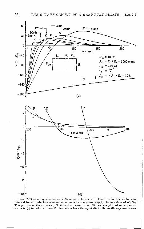
80 -125mh
0 0t in 4 sec
g -40 -I~ i?: = Rt + Rc = 1000 ohmsL“ -80 -
-120 - ~Lc =Oj Rt+Rc=lOk
-160
-200 (a)
\
FIG, 2.39.—Storage-condenser voltage as a funct,on of time during the recharginginterval for an inductive element in series with the power supply; large values of R’. /L..The portion of the curves C, D, E, and F beyond t = 150p sec are plotted on expandedscales in (b) in order to show the transition from the aperiodic to the oscillatory conditions.

SEC. 25] AN INDUCTANCE AS THE ISOLATING ELEMENT 67
To illustrate the effect of the inductance of the isolating element onthe charging of the storage condenser, the six curves shown in Fig.2.39a have been plotted using the values of [Vc(~) – llb~] calculatedfrom Ikqs. (88) and (89) forvarious values of L.. The calculations weremade for R: = 1000 ohms, Ebb = 10 kv, and C~ = 0.05 yf in the circuitof Fig. 2.36a. Since the equations for V.(t) involve the terms (Eb, – V,)and io, it was also necessary to specify a particular pulse duration. Fol”these calculations r = l~sec was chosen, and the assumptions weremade that R. = rP for all values of L., and that the voltage on the storagecondenser was equal to Ebt, at the start of the puke. The values of(EM – V,) and io used in the calculations were therefore obtained fromthe relations.
(E,, – V,) = &i-.W
andEbb
io=—f.L.
For the values of the circuit parameters given above, (EW – V,) = 200volts and io = 10–2/L. amp.
The curves .4 and B are obtained for L, equal to 5 mh and 10 mhrespectively. These values of L. are less than the value for critical damp-ing, so curves A and B are aperiodic. When L, = ~R~Cm = 12.5 mh,the curve C is obtained, which corresponds to the critically dampedcondition. Curves D, E, and F are oscillatory, ~vith L. equal to 16 mh,25 mh, and 50 mh respectively. The value of 25 mh corresponds toL. = ~R~Cw, producing the maximum frequency for the oscillation.Portions of the curves C, D, E, and F are plotted in Fig. 239b with anexpanded ordinate scale in order to show the details of the curves whenL. is larger than the value for critical damping. The curve G in Fig.2.39a shows the effect of a 10,000-ohm noninductive resistance as theisolating element, and is included to emphasize the rapid buildup of thecondenser voltage when an inductance is used.
The curves of Fig. 239 also apply for values of C~ other than 0.05 pfif R{, Ebb, and r are not changed and a scale factor is introduced. Withthe scale factor K cc (Ebb – V,)/R~, the ordinate scale corresponds to[Vc(t) – Et,b]/K and the abscissa scale is Kt. The condition is imposedthat
(Cw), (L.), 1Oxj = m, = R’
where the values of (L.) 1 are those that correspond to the curves of Fig.2.39 for wh~ch K = 1. Thus, if (C~) z = O.Ol~f, the scale factor is 5and (L.)i for curve A, for example, is 1 mh. The curves C and E again

68 THE OUTPUT CIRCUIT OF A HARD-TUBE PULSER [SEC. 2.5
correspond to the critically damped and the maximum-frequency condLtions respectively.
To illustrate the effect of small damping on the charging of the storagecondenser, the curves shown in Fig. 2“40 were calculated from Eq. (88).For the three curves A, B, and C a value of R~/Lc = 10 ohms per mh wasused with C. = 0.05 pf, EM = 10 kv, and ~ = 1 psec. The values ofL. are 5 mh, 10 mh, and 20 mh, respectively, for the curves A, 1?, and C.The effect of adding some resistance in series with Lo is indicated by thecurve A’ for which L. = 5 mh and R: = 500 ohms. These curves are
600 r A..
400 -
200 -
i~k“ o
-200
-600-FIO. 240.-Storage-condenser voltage as a function of time during the recharging
interval for an inductive element in series with the Power supply; small values of R’. /L..For curves .4, B, and C the value of R’t/L. is 10 ohms per mh with ~.= 5 mh, 10 mh, and20 mh respectively. For curve A’, ~. = 5 mh and R’. = 500 ohms. Et.b = 10 kv andCu = 0.05pf for all curves.
indicative of the way in which the storage-condenser voltage varies duringthe interpulse interval if small inductances and small values of RJL. areused both for the isolating element and for the recharging path Z, ofFig. 2.36b.
There are two principal advantages to be gained by the use of aninductance as the isolating element. The possibility of having the con-denser voltage equal to the power-supply voltage at the start of each pulseprovides better utilization of the available power-supply voltage. Also,the power dissipated in the resistance associated with the inductancecan be less than in the case of a high-resistance isolating element. Inany pulser design, these advantages must be weighed against the undesir-able possibility that the recharging of the condenser may be oscillatory,and also against the increase in current through the switch tube withtime during the pulse interval. The latter consideration is perhaps themore serious, since it may cause a larger drop in pulse voltage during the

SEC. 25] AN IN I) I’CTA NCE AS THE ISOLA TI,VG ELE,J[ENT 69
pulse than that which results from the change in the storage-condenservoltage.
The more rapid increase in the storage-condenser voltage during theinterpulse interval, ~vhich is possible with the inductive isolating element,can be used to advantage in pldsers designed for closely spaced pulses,part icularly if the int erpulse intervals are of nonuniform duration, as inthe case of pulse coding.
When an inductive element is used in parallel with the load in orderto bring the trailing edge of the puke down rapidly, as discussed in Sec.23, this inductance becomes part of the recharging circuit as ~vell. Thecurrent floiving in the ind~lctance may be oscillatory and of sufficientmagnit~ldc to exert consi{lerahlc inflllcnce on the initial conditions for therecharging cvcle. It is therefore obvious that a complete analysis of therecharging of the storage condcnscr is too complex to permit as detailedconclusions to be drawn as are possible in the case of the resistive isolatingelement.
POWER TRANSFER TO THE LOAD
One of the important consi(lerations involved in the design of a pulseris the magnitude of the p(llse poit-er to be delivered to the load. Thispulse polrcr is etlual to the product of the voltage ancl current during thepulse. If the pu]aes of \-oitage and current are constant in amplitude for\tle pulse duration, the trrms “pulse po\rer” and “ peak po~ver” have;he same significance. lVhcn the pulsc amplitude is not constant during,he pulse, the peak power refers to the maximum voltage-current product,ml the pulse power is the product Ofan average amplitude for the voltagemd current pu]scs. There are several possible methods by \vhich thisiveraging may be done (see .Ippendix B). For the hard-tube pulser,thevoltageand ~Urr~nt plllsrs !Yner:dly have a top that is relatively flat,md the meaning of “average pulse amplitude” is reasonably clear.For the present discussion the term [‘pulse po~ver” refers to the averagevoltage-current product for pulses that do not deviate very much fromconstant arnplitu(lc.
It may he necessary to have some circuit elements in parallel ~viththo load in order to change pulse shape or to provide a recharging pathfor the storage condenser, as sho\rn in Sees. 2.2 and 2.3. Some po!ver is(Iissipatwl in these sh(mt elements, and this polrer must be taken intoaccollnt in (Iesigning a pulscr for a given poiver output to a load. Byrareful desi~n, ho!vever, it is generally possible to make the poiver losssmall romparwl \vit,h thr load pulse polrer. The present discussion ofpo!ver transfer to the load on a hard-tube pulser is simplified by the:Lss(lmption that any shunt losses may be considered as part of the pulser]v:ld.

70 THE OUTPUT CIRCUIT OF A HA A?D-TUBE PULSER @EC.2+
It is evident from the circuit of Fig. 2“5 that the current through theswitch tube is approximately equal to the current through the load.Also, the pulse voltage across the load is approximately equal to thepower-supply voltage minus the voltage drop in the switch tube. Theseconsiderations are of fundamental importance in the design of a hard-tube pulser when a definite load impedance and pulse-power output arespecified. The connection of the load to the pulser as indicated in thecircuits discussed in Sees. 2“2 and 2“3 is referred to as a” direct-connection. ”
If the pulse power and the load impedance are specified, the requirements for the switch tube and the power supply are almost completelydetermined for the load dhectly connected to the pulser. Thus, if thepulse power is PI and the load impedance is R, the pulse voltage isV1 = -l and the load current is II =. @z/Rz. The switch tubemust therefore be chosen so that the current 11 can flow without makingthe voltage drop in the tube too high. When the magnitude of this volt-age drop is known, the required power-supply voltage is also known.The switch tube must also be capable of withstanding the power-supplyvoltage during the interpulse interval. The switch tubes that havebeen available for microwave-radar applications of hard-tube pulsershave had effective resistances ranging from about 50 ohm: to severalhundred ohms. Most of these tubes have a maximum current-carryingcapacity that is determined by available cathode emission or by electrodepower dissipation. For pulsers with low average power, the cathodeemission determines the maximum current, and for pulsers with highaverage power, the allowable electrode power dissipation usually imposesthe limit on the current. The effective resistance introduced into thepuise circuit by the switch, tube is relatively constant over the usablerange of current, except for special design, such as operation on the flatportion of the pulse characteristic of a tetrode (see Chap. 3).
2.6. Impedance-matching and Pulse-transformer Coupling to theLoad.-A hard-tube pulser may be considered as a generator with aninternal impedance equal to the effective resistance of the switch tube.If the resistance of the load is high compared with the generator internalresistance, the eficiency is also high but the power delivered to the loadis small compared with the maximum power that could be obtained. Itis shown in most textbooks on electricity that the maximum power isdelivered to a load when the load and generator resistances are equal.This condition means, however, that as much power is lost in the gen-erator as is delivered to the load, and the eficiency is only 50 per cent.Shce a maximum of 50 per cent efficiency can not be tolerated in mosthard-tubepulser applications, impedance-matching is seldom used.
Impedance-matching is important in the line-type pulsers to be dis-cuswd in Part II. Since for these pulsers the internal impedance is

SEC. 2.6] IMPEDANCE-MATCHING 71
nondissipative, the above-mentioned difficulty for hard-tube pulsers isnot encountered. It is possible, however, to achieve some gain in hard-tube pulsers designed for low pulse-power output by changing the loadimpedance presented to the pulser. In particular, it is possible to use alower power-supply voltage for a given pulse power into a high-impedanceload if a pulse transformer is used to transform the load impedance toa lower value at the pulser output terminals. The details of pulse-transformer design and construction are given in Part III.
A brief discussion of the considerations involved in the use of a pulsetransformer with a hard-tube pulser serves to indicate when such anarrangement is advantageous and to point out the limitations. Forthis purpose, the hard-tube pulseris represented as a battery in serieswith the switch-tube resistance, asshown in Fig. 2.41. The primary ofthe pulse transformer is connectedto the pulser output terminals, and -m’’DR’the load is connected across the sec- NF N~ondary. The secondary is considered FIG. 2.41.—Equivalent circuit for a
to have rz times as many turns as hard-tube pulser with pulse-transformer
the primary, and the power-transfercoupling to the load.
efficiency, q, of t,he t,rausformer is assumed to be determined only by shunt
losses. This assumption is justified by experience with such trans-
formers in the microwave-radar applications. The following relationsmay then be written:
and
thus
V.9T,
=n
lfIpI,=y.
The power into the load is
(90)
(91)
(92)
(93)
andVp = Vw – IprP, (94)Vs = IsRi, (95)
where the switch-tube current 1= is equal to the primary current 1P andthe load current It is equal to the secondary current I,. Combiningthese relations, the expression for the load power becomes
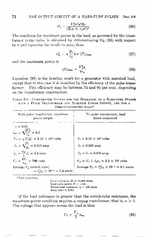
72 THE OL’TPL:T CIRCUIT OF A HARD-TL7BE PULSER [SEC.2.6
V~n2q2Rl
‘z = (Z?lq + rPn2)2”(96)
The condition for maximum polver in the load, as governed by the trans-fornwr turns ratio, is obtained by differentiating Eq. (96) with respectto n an(l equating the result to zero; thus,
and the maximum power is
(P,)max= p.P
(97)
(98)
Equation (98) is the familiar result for a generator with matched load,except that in this case it is modified by the efficiency of the pulse trans-former. ‘I’his efficiency may be between 75 and 95 per cent, dependingon the transformer construction.
TABI.~ 2 1.—~OMFARATIVE VA1.UES FORTHEOPERATIONOFA HARD-TUREPULRERWITHA PULSETR.*SSFORMER.ASDMAXIMUMPOWEROUTPUT,ANDFORA
DIRECT-CONNECTEDLOAD*
\\ltb PLLISCtransformer, nlaximumpo!ucr output
q = 0.85
JR m
71,. = ~ = 9.2
1“/ = ~ = 3.16 X 10³\rolts
<P,
I, =Et
= 0.316 amp
AveragePp (switchtube)= I~rPX 10-3 = 1.2 watts
X-opulsetransformer,loaddirect-connected
VI = 3,16 X 10³volts
II = 0.316 amp
1. = I! = 0.316 amp
VW= Vi + 1.?9 = 3.2 X 10³volts
AverageP= = I~rP X 10-3 = 0.1 watts
* Tmtccmditiom;Load resistance, R, = 10,000 ohms.Load pulse power, Pi = 1kw.Switch-tube resistance, rp = 100 ohms.Duty ratio = 0.001.
If the load resistance is greater than the switch-tube resistance, themaximum-power condition requires a stepup transformer, that is, n > 1.The voltage that appears across the load is then
(99)

SEC.2.6] IMPEDANCE-MATCHING 73
and the switch-tube current is
(loo)
The significance of these considerations is best brought out by com-paring the values of the pulser parameters for the case of the direct-connected load on the one hand and that of the transformer-coupled loadwith maximum power output on the other hand. The results are givenin Tables 2”1 and 2.2 for two values of load resist ante and pulse power.
TABLE2.2.—COMPARATIVEVALUESFORTHEOPERATIONOFA HARD-TUREPULSERWITHA PULSETRANSFORMERANDMAXIMUMPOWEROUTWJT,ANDWITHA
DIRECT-CONNECTEDLOAD*1
With pulse transformer,maximum~
No pulse transformer,loadpower output direct-connected
I
~ = 0.85
<R mn.= F= 2.9
V1 = ml = 10’ ~olts I v,= 104volts
I11= 10 amp
1, = ‘~ I, = 34 amp I1,=II=10 amp
v _~=7x10, vo,t~.-nm I v. = V[ + Ipr, = 11 x 103volts
Average”~p(switchtube) = 120watts AverageP, (switch tube) = 10 watts
* Teat conditions:Load resistance, R, = 1000ohms.Load pulse power, Pi = 100kw.Switch-tube resistance, r, = 100 ohms.Duty ratio = 0.001.
Examination of these tables indicates that, with the 10,000-ohm loadand l-kw pulse power, the gain in using the pulse transformer is large asfar as power-supply voltage is concerned. The switch-tube current ismore than ten times the load current, but is still within the operatingrange of available tubes. The power dissipation of 1.2 watts in theswitch tube is also not prohibitive. The question to be decided in thiscase is whether or not the reduction in power-supply voltage, from about3 kv to 700 volts, is important enough to warrant the use of a switchtube that can pass a current of 3.4 amp with the additional power loss ofapproximately one watt.
For the 1000-ohm load and 100-kw pulse power, the increase in switch-tube current from 10 amp to 34 amp produced by using the pulse trans-former and maximum power design is generally more serious than the

74 THE OUTPUT CIRCUIT OF’ A HARD-TUBE PULSER [SEC.2.6
factor of 10 increase in the previous case. A relatively small tubelcan be used to provide the 0.3 or 3.4 amp, whereas the increase in platevoltage from 700 volts to 3 kv may both increase the size of the tube andimpose greater problems in its fabrication. The increase in tube cur-rent from 10 amp to 34 amp, however, may necessitate the use of two orthree tubes in parallel or the use of a larger cathode, which is generally aserious moblem in tube manufacture. For tubes that have been avail-able fo~ the microwave-radar applications, the gain introduced by thereduction of plate voltage from 11 kv to 7 kv does not offset the difficultiesintroduced by the increase in plate current. The increase of more than100 watts in power dissipation in the switch tube also imposes a moreserious problem than the l-watt increase for the 10,00@ ohm load.
These examples show that the use of a pulse transformer to reduce thenecessary power-supply voltage is not a priori always advantageous topulser design. However, the pulse transformer is not used only to givethe maximum power output. There are situations in which a smallreduction in the necessary power-supply voltage may be warranted atthe expense of slightly higher switch-tube current. Under these condi-tions, it is necessary to use Eq. (96) for power output in terms of thecircuit parameters in order to determine the design best suited to theavailable components.
The above design considerations lead to the minimum values ofswitch-tube current and power-supply voltage for a given load impedanceand pulse power. To these values must be added any contributionsresulting from the connection between the charging circuit and the dis-charging circuit as discussed in Sees. 2-I and 25. These contributionscan usually be kept small, but in some cases, such as a design for closelyspaced pulses, it may be necessary to allow for increases of as much as25 to 50 per cent above the minimum values.
ti#R+iizE(a) (b)
Fm. 2.42.—Two possible arrangements for the use of a pulse transformer with a hard-tubepulser.
A pulse transformer maybe used with a hard-tube pulser in either oftwo ways. The two possibilities, with a triode as the switch tube, areshown schematically in Fig. 2.42. In Fig. 2.42a the primary of the pulse
1R. B. Woodbury, “ Pulse Characteristicsof Common Receiver Type Tubes,’;RL Report No. 704, Apr. 30, 1945. Seealso tube data given in Chap. 3.

SEC.26] IMPEDANCE-MA TCHING 75
transformer takes the place of the load in the circuits of Sec. 2.2. Inthe circuit of Fig. 2.42b the storage condenser is eliminated and the pulse-transformer primary is in series with the power supply and the switchtube. It has been mentioned previously that, from a practical stand-point, some part of the circuit must beat ground potential, and reasonswere given for connecting the switch-tube cathode, rather than the plate,to ground. Thus, if point g is connected to ground in Fig. 2.42a, oneend of the pulse-transformer primary is grounded, and the winding mustbe insulated only for the maximum pulse voltage. If the cathode of theswitch tube is connected to ground in the circuit of Fig. 2.42b, the primaryof the transformer must be insulated for the d-c power-supply voltage.This voltage is greater than the pulse voltage by the amount of thevoltage drop in the switch tube, which may amount to 10 to 20 per centof the power-supply voltage. The problem of providing adequate insula-tion for d-c voltages in such a transformer is somewhat more serious thanfor an equivalent pulse voltage. This difficulty causes a transformerdesigned for the circuit in Fig. 2“42b to be somewhat inferior to a trans-former suitable for the circuit of Fig. 2“42a as regards the effect on pulseshape. There is a greater deviation from a rectangular pulse shape atthe load because of the less satisfactory ratio of leakage inductance todistributed capacitance in the transformer. The transformer forcircuit in Fig. 2.42b may also have a somewhat lower power-transferefficiency.
There is a further argument in favor of the use of a storage condenserwith pulse-transformer coupling to the load. If the load is a magnetronor some other device that may exhibit sudden changes in impedancebecause of sparking or voltage breakdown, a high-voltage surge occurs atthe plate of the switch tube. This transient voltage may be sufficientto cause the switch tube to spark internally, thus vitiating the control ofthe grid over the tube conduction. When the grid loses control, the timeduring which the switch tube is conducting may exceed the desired pulseduration by a large factor. In the circuit of Fig. 2.42b this behaviorcauses more energy to be discharged into the load than that correspondingto the normal pulse, with the result that the sparking condition is aggra-vated. In the circuit of Fig. 242a, the same sequence of events is not asse -ious, since the available energy in the storage condenser is considerablyless than that in the filter condensers of a power supply. Because of theinherent characteristics of a pulse transformer, it is actually possible touse a smaller capacitance for the storage condenser in the circuit of Fig.2.42a than that necessary for a direct-connected load in order to obtain agiven flatness for the top of the pulse.
If a pulser is designed to use a pulse transformer and no storage con-denser, the versatility of the unit is decreased. A pulser of the type

76 THE OUTPUT CIRCUIT OF A HARD-TUBE PULSER [SEC.27
shown in Fig. 2.42a can be used equally well with a direct-connected loadwithin the limits of its design. With a load substituted for the pulsetransformer in the circuit of Fig. 2.42b, the load or the switch tube mustbe operated at high d-c potential with respect to ground.
2.7. The Effect of Stray Capacit ante on the Pulser Power Output.—When the duty ratio is high, the average-power considerations may out-weigh the pulse-power requirements in governing the choice of com-ponents for the pulser. As has already been mentioned, the switch-tubedissipation can impose a limit on the maximum allowable pulse current.The choice of the capacitance for the storage condenser is also affected bya high-duty-ratio requirement, but in different. ways depending onwhether the high duty ratio is due to a long pulse duration, or to a highrecurrence frequency. Thus, if the pulse duration is long and the inter-pulse interval is also long, the storage condenser must have a highcapacitance in order to keep the pulse current as constant as possibleduring the pulse. When the recurrence frequency is high, ho~vever, theinterpulse interval is small, and the condenser capacitance must be assmall as possible to best utilize the power-supply voltage, and it mayalso be necessary to have a higher current from the power supply duringthe pulse interval.
The stray capacitance in parallel with the pulser load becomes anImportant consideration when the recurrence frequency is high and thepulse voltage is large. This capacitance becomes charged during thetime required for the pulse voltage to build up, and its discharge startswhen the switch tube becomes nonconducting. The energy stored inthis capacitance, therefore, does not contribute to the pulse power inthe load except during the time corresponding to the trailing edge of thepulse. The average-power loss that corresponds to the charging of thiscapacitance is simply the energy stored per pulse multiplied by thenumber of pulses per second, that is,
PRF X lC,g~,
In the example used for the values of Table 2“2, a stray capacitance of100 ppf introduces a loss of about 5 watts if the 0.001 duty ratio corre-sponds to a PRF of 1000 pps. At a PRF of 10,000 pps, ho~vever, thispower loss is 50 watts, which is one half of the average power delivered tothe load.
The current required to charge the stray capacitance also has aninfluence on the pulse power for which the pulser is to be designed. Ifit is desired to have a high rate of rise for the voltage pulse, the current-carrying capabilities of the switch tube must satisfy the relation
dVlIC = Cs ~.

SEC. 2.8] OUTPUT POWER REGULATION 77
If the value 100 p~f is again taken as an example, this current is 10 ampfor dVJdt = 100 kv/~sec, which corresponds to a time of rise of O.lpsecfor a 10-kv pulse. In the example used for the values of Table 2.1, aswitch tube capable of carrying 0.5 amp is adequate for the direct-con-nected load, but the maximum dVJdt is then 5 kv/psec, correspondingto a time of rise of 0.6 ysec for a 3-kv pulse. Thus, the peak-currentlimitation for a particular switch tube may be high enough to satisfythe load pulse-power requirement and still limit the maximum rate ofrise of the pulse voltage.
2.8. Output Power Regulation.-The change in output power from ahard-tube pulser, which is caused by a change in the power-supply volt-age, may be expressed in terms of the switch-tube and load characteristics.This relation is of practical importance in pulser applications because itgives an indication of the stability of the power output as a function ofthe voltage input to the pulser. If the change in the power output isAPl, the ratio APJPl, expressed in terms of the ratio AELJEw for thepower-supply voltage and the circuit parameters, gives the regulation ofthe output power. Thus, for a given set of conditions, the regulation isdetermined by the relation
(101)
If k is large, the regulation is poor, that is, the percentage change in out-put power is large compared with the percentage change in power-supplyvoltage. Conversely, if k is small, the regulation is good.
The value of k in Eq. (101) depends on the pulser parameters and onthe load characteristics. In order to find an expression for k, let it beassumed that a biased-diode load is used, and that the voltage on thestorage condenser differs very little from the power-supply voltage. Thepower into the load is
Pl = VIIl (102)and
Vt – v.II = —J
T1(103)
where V, is the bias voltage and rz is the dynamic resistance of the load.The voltage across the load is
VI = Eti – IlrP, (104)
where the effects of elements in parallei with the load and of the recharg-ing circuit are neglected in considering the switch-tube current. Com-bining Eqs. (102), (103), and (104), the expression for the power becomes
P1 = (105)

78 THE OUTPUT CIRCUIT OF A HARD-TUBE PULSER [SEC. 29
Differentiating Eq. (105) with respect to Ebb and forming the ratioAPJPl, there is obtained
If the load dynamic resistance is equal to the switch-tube resistanceand the bias voltage in the load is 0.8 times the power-supply voltage,Eq. (106) gives
APL AEbb ~ 2 g%.PC = Ebb 1.8 X 0.2 = 5“6 Ebb
(107)
Thus, for these conditions, the percentage change in the output power isabout six times as large as the percentage change in the power-supplyvoltage, Since the values chosen for this example are typical for themedium-power magnetrons used in microwave radar, this result isimportant in pulser applications with magnetron loads.
If the bias voltage is zero, that is, V. = O, Eq. (106) becomes
(108)
The power regulation for a pure-resistance load is therefore considerablybetter than that for a magnetron or biased-diode load.
In the discussion of Chap. 3, it is shown that advantage maybe takenof the characteristics of tetrodes as switch tubes in order to improve thepower regulation for a hard-tube pulser. As in any power-generatingdevice, however, improved regulation is obtained at the expense ofadditional power loss.
2.9. Effects of Pulse-transformer Coupling to the Load. —There arethree principal advantages to be gained by coupling the output of ahard-tube pulser to a load by means of a pulse transformer. One ofthese has already been indicated in the discussion of Sec. 2.6, namely,that a transformation of the load impedance can be accomplished with apulse transformer, that is, the impedance presented to the output of thepulser can be made either higher or lower than the load impedance. Again in voltage, current, or power at the load can be obtained in thismanner for given pulser and load characteristics. Another advantage is
obtained by the use of two pulse transformers, a stepdown transformer atthe pulser output terminals and a stepup transformer at the load, with alow-impedance cable between them. This arrangement facilitates thephysical separation of the load and the pulser, which is a desirable engi-neering convenience in many cases. The third advantage of transformer

SEC.2.9] EFFECT OF A PULSE TRANSFORMER 79
coupling is that it provides a means of reversing the polarity of the pulseat the load. The use of two pulse transformers with different turnsratios for the stepup and stepdown transformers makes it possible toobtain all three of the advantages simultaneously.
In microwave applications, pulse transformers are used with hard-tube pulsers primarily because of the advantages to be gained by thephysical separation of the load and the pulser. Serious difficulties arisein transmitting high pulse power and the correspondingly high pulsevoltage more than a few feet from the pulser to the load. The use ofstepdown and stepup pulse transformers makes it possible to transmit thepulse power at relatively low voltage over flexible coaxial cable for dis-tances as great as several hundred feet. Associated with this addedconvenience, however, there is some power loss, some pulse-shape dis-tortion, and sometimes increased backswing voltage. In any given case,therefore, it is necessary to weigh these disadvantages against theadvantages. The purpose of this section is to indicate the extent towhich the disadvantages may affect the design of the hard-tube pulser.
The theory of pulse transformers and the considerations involved intheir design and construction are given in detail in Part III. There it isshown that the equivalent circuit for a pair of pulse transformers may be
Output termmals of ahard.tube pulser
(LL)l Cable (LI, )2
4 &m-) jivL,, R, L, [.r
!= .1
s,LC 1>, R, [.,,
tVp u v,
J =:,, ‘, ‘_ =; ,, =,.
c~ cc cc r,/,c, = v,
TI
Stepdown Stepuptransformer transformer
FIG. 243.-Equivalent circuit for a stepdown anda stepuppulse-transformercombinationfor a hard-tube pulser and a biased-diode load,
represented as in Fig. 243. The elements L., L., and Cc are associatedwith the low-voltage winding of the transformer, which is referred to as theprimary, L. being the effective shunt inductance and C’c the distributedcapacitance of this winding. The so-called “charging inductance,”Lc, is introduced to account for the nonuniform current distribution alongthe coil corresponding to the flow of charge into Cc. The element L~ isthe leakage inductance, R, represents the effective shunt loss in the trans-former, and L. and C. have the same significance for the high-voltage
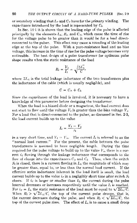
80 THE OUTPUT CIRCUIT OF A HARD-TUBE PULSER [SEC.2.9
or secondary winding that Lc and Cc have for the primary winding. Thecapacitance introduced by the load is represented by Ct.
In Sec. 14.1 it is shown that the leading edge of the pulse is affectedprincipally by the elements L~, R,, and c., which cause the time of risefor the voltage pulse to be greater than it would be for a load direct-connected to the pulser. This effect may cause a rounding of the leadingedge at the top of the pulse. \Vith a pure-resistance load and no biasvoltage, this increase in the time of rise for the pulse voltage becomes verynoticeable. The best design of a pulse transformer for optimum pulseshape results when the static resistance of the load
~,=~,=
d:
zLL
11 c’
where XL= is the total leakage inductance of the two transformers plusthe inductance of the cable (which is usually negligible), and
C= CD+C1.
Since the capacitance of the load is invol~’ed, it is necessary to have aknowledge of this parameter before designing the transformer.
lYhen the load is a biased diode or a magnetron, the load current doesnot start to flolv until the voltage V~ is greater than the bias voltage V,.
For a load that is direct-connected to the pulser, as discussed in Sec. 2.3,the load current builds up to the value
in a very short time, and J’~ = V.. The current Zt is referred to as the“ normal load current. ” For the present, the cable between the pulsetransformers is assumed to have negligible length. During the timerequired for the pulse voltage to build up to the value V,, there is a cur-rent z’Cflowing through the leakage inductance that corresponds to theflow of charge into the capacitances C,, and Ct. Thus, when the switchSt is closed, there is a current flowing in LL the magnitude of which maybe greater than, equal to, or less than the normal load current. If theeffective series inductance inherent in the load itself is small, the loadcurrent builds up to the value ic in a negligibly short time after switch Stcloses. If ic is larger or smaller than 11, the current during the pulseinterval decreases or increases respectively until the value Z1is reached.For z’C= 1,, the static resistance of the load must be equal to V-.\\’hen R, > v’-, the top of the current pulse droops, that is,the current decreases during the pulse, and when R1 < v’”C, thetop of the current pulse rises. The effect of L. is to cause a small droop

SEC. 2.9] EFFECT OF A PULSE TRANSFORilfER 81
in the current pulse even for the optimum value of ~~. A seriesof oscilloscope traces that illustrates the foregoing statements is remw-.-duced in Figs. 2.44 and
(a) Fti > 1100 ohms
(d) RI > 1100 ohms,
(o) RL> 1100 ohms.
2.45.
(b) R, = 1100 ohms,Magnetron current pulses.
(e) Ri = 1100 ohms,Magnetronvoltage pulses,
(c) Rt < 1100 ohms.
(f) RI < 1100 ohms,
(h) R~ = 1100 ohm,. (z) R( < 1100 Ohll]SVoltage pulses at the input terminals of the stepdown transformer.
FIG. 244.-Oscilloscope traces for 2-Psec pulses of magnetron current, magnetronvoltage, and pulser output voltage for a hard-tube pulser with pulse transformers and 6 ftof 50-ohm pulse cable. The 232AW stepdown and the 232BW stepup transformers, forwhich v/ ZL~/C = 1100 ohms, were used for these traces.
The effect produced by the effective shunt inductance and trans-former losses may be seen by comparing the pictures of Figs. 2.44 and 2.45

82 THE OUTPUT CIRCUIT OF A HARD-TUBE PULSER [SEC. 2.9
for the cases where RI = V 2L./C. It is to be observed that the currentpulse droop is greater for the 135A W-14 lBW transformer combination
(a) R, > S80ohms, (b) r = Sso011111s. (c) Rt <880 ohms.Maguetrou current pulses.
(d) R~ > 880ohms, (e) R, = 8S0 ohms. (-f) RI <880 ohms.Magnetronvoltagepulses.
(LJ)IZ[ >880 ohms. (h) R, = 880 ohms. (i) R/ <880 ohms.Voltage pulses at the input terminals of the stepdown transformer.
~lG. ~45.-@Cdl06C0pe traces for j?.psec pulses of magnetron Current, magnetronvoltage, and pulser output voltage for a hard-tube pulser with pulse transformers and6 ft of 50-ohm pulse cable. The 135.\W stepdown and the 141B\V stepup transformers,for which #XLL/C = 880 ohms, were used fcr these traces.
than for the 232 AW-232BW combination. The latter pair of trans-formers have higher efficiency as determined by calorimetric measure-ments of power loss.

SEC. 2.9] EFFECT OF A PULSE TRANSFORMER 83
When the current in the leakage inductance is greater or less thanthe normal load current, the rate at which the pulse current decreases or
(a) I& >1250 ohms. (b) Rt = 1250 ohms.Magnetron current pulses.
(c) RI <1250 ohms.
(d) RI > 1250 ohms. (e) R, == 1250 ohms. (J) R, <1250 ohms.%fagnetron voltage pulses.
(u) R >1250 ohms. (h) R! = 1250 ohms. (0 R[ <1250 ohms.Voltage pulses at the input terminals of the stepdown transformer.
FIG. 2.46.—Oscilloscope traces for 2-psec pulses of magnetron current, magnetronvoltage, and pulser output voltage for a hard-tubs pulssr with the 232AW and the 232BWpulse transformers and 175 ft of 50-ohtir pulse cable. The 50-ohm cable impedance istransformed to 1250 ohms at the output of the pulser and the input to the magnetronbecause the turns ratio for each transformer is 1 to 5. The transit time for the trans-formers and cable is 0.42Wec.
increases during the pulse depends on the time constant ~LL/ (~~ + @,where r= is the internal resistance of the pulser. For the 232 AW-232BWtransformer combination and the magnetron used to obtain the oscil-loscope traces of Fig. 2.44, this time constant is about 0.3 Psec, whereas

84 THE OUTPUT CIRCUIT OF A HARD-TUBE PULSER [SEC. 2.9
for the 135AW-141BW combination it is about 0.18 psec. This dif-ference is observable in the pictures of Figs. 2.44 and 2.45.
Reelection Effects Caused by Impedance Mismalch with Long Cable.—
Another effect is observed when the cable is so long that the time requiredfor the pulse to travel from one transformer to the other is an appreciablefraction of the pulse duration. Discrete steps appear on the top of thecurrent pulse as a result of an impedance mismatch between the loadand the cable. Some photographs of oscilloscope traces showing thisphenomenon are reproduced in Figs. 2“46 and 2“47 for the 232AW-232BW
(a) RI >1250 ohms.Magnetron current pulses.
(c) R, > 1250 ohms (d) R, = 1250 ohms.Magnetron voltage “pulses.
FIG. 2.47.—Oscilloscope traces for 2-psec pulses of magnetron current and voltage for ahard-tube pulser using the 232AW and 232BW pulse transformers with 100 ft of 50-ohmpulse cable. The transit time for transformers and cable is 0.25Wec.
transformer combination and 175 ft and 100 ft of 50-ohm coaxial cable.These transformers have a turns ratio of 5/1 for the secondary and pri-mary coils. Thus the 50-ohm impedance of the cable is transformedinto an impedance of 1250 ohms at the high-voltage windings of thetransformers.
The combination of pulse-transformer and cable may be consideredas a transmission iine of characteristic impedance 20 = 1250 ohms.If the impedance of the load is different from 1250 ohms, a voltagereflection occurs whose magnitude and sign depends on the reflectioncoefficient
21 – 20‘= 21+2.”

SEC. 2.9] EFFECT OF A PULSE TRANSFORMER 85
Let VP be the pulse voltage at the pulser output and let 6 be the timerequired for the pulse to travel in one direction through the transformersand the cable. 1 If VI denotes the pulse voltage traveling from thepulser to the load, the magnitude of VI at the pulser is VP. Becausethere is some attenuation of the pulse voltage in traversing the trans-formers and cable, the voltage appearing at the load end is kVi=, wherek <1. When Z1 > Zti, the reflection coefficient at the load is positive,and the reflected voltage is
()z, – ZoV: = kVP -o . (109)
This voltage therefore adds ta the incident voltage at the load, producingan actual load voltage
‘V’)l ‘kvp+v’=kv41+(%w(110)
The load pulse voltage can be larger than the output voltage of the pulser,M in the first series of pulse pictures of Fig. 2.46.
The reflected voltage travels back toward the puleer, where it is againreflected. At the pulser the reflection coefficient
z, – z,‘= ZP+ZO’
where ZP is the internal impedance of the pulser. For a hard-tubepulser Z, is merely the switch-tube resistance r,. Since, in general,Zp is considerably less than 1250 ohms, the reflection coefficient is nega-tive, and the polarity of the reflected voltage is opposite to that of themain-pulse voltage. At a time 26 after the start of the pulse at the pulseroutput, the voltage at the input terminals of the stepdown pulse trans-former is
v: = Vp + kv; + V2, (111)where
‘,=kv’(%a (112)
The pulse voltage traveling away from the pulser toward the load is nowV, + Vz, which is less than VP because V2 is of opposite polarity to V,.
At the time 36 this new pulse voltage appears at the load, where a reflec-tion again occurs such that
()ZI – ZoV:= k(V, + V,) -o ~ (113)
1The velocityof propagationin the cablesusedwithpulsersfor microwaveapplica-tions is about 450 ft/p sec. The observedtime delay in the picturesof Fig. 246 is0.42 paec,indicatingthat the two transformersintroducea delay of about 0.03 psec inaddition to that of the cable.

86 THE OUTPUT CIRCUIT OF A HARD-TUBE PULSER [SEC. 2.9
and the load is subjected to a voltage
[ (=)1 ““)(v,),= k(v,+ v,) + Vj= lc(v,+ v*) 1+
Since (V, + V,) < V,, the pulse voltage at the load changes suddenlyat time 3ti from the value given by Eq. (110) to that given by Eq. (114),producing the first step that appears in the pictures of Fig. 2.46.
If the pulse duration is several times longer than 26, a succession of
Fx~. 2.48. =Skitch of volt-age and current pulses indicat-ing the stepsresultingfrom animpedance mismatch betweentheloadandthecablewhentwopulsetransformersare used witha hard-tube pulser. The loadimpedance is greater than thecable impedance referred to thehigh-voltage windings of thetransformers.
these steps occur as indicated in the sketchof Fig. 2.48. The successive steps becomeprogressively smaller, as evidenced by thefact that (Iz)3 and (11), in Fig. 2.47 are al-most equal. These pictures were obtainedwith the same transformers and magnetron,but with 100 ft of cable instead of the 175ft used for the pulses shown in Fig. 2.46.
When the impedance of the load is lessthan that of the cable, the steps are in theopposite direction, as can be seen in the thirdseries of pictures in Fig. 2.46. As a result ofthe change in load impedance during the timethe pulse voltage is built up, reflections ofshort time duration occur. The effect ofthese reflections is evident from the secondseries of pictures in Figs. 2.46 and 2.47, inw,hlch the load and cable impedances are ap-proximately equal. Small irregularities occurat the times corresponding to the steps in theother two series of pictures.
As an example of the foregoing discussion,the experimental and calculated values corresponding to the first series ofpictures in Fig. 2.46 are given. The voltage at the pulser output is
V, = 8.55 kvand that at the load is
(V,), = 9.36 kv9“, mce
(I,), = 4.82 amp,
(z,) , =9.36 X 10³
4.82= 1940 ohms.
The reflection coefficient at the load is therefore
zl – Zo 1940 – 1250 = 0,216— .ZI + Zo 194o + 1250 ‘

SEC.29] EFFECT OF A PCLSE TRANSFORMER 87
and the value of k may be determined with the aid of Eq. (110), that is,
k=9.36 x 10’
8.55 X 103 X 1.22= 0.9
The reflected voltage traveling toward the pulser is then
l’; = 0.9 X 855 X 103 X 0.216= 1.65 kv.
The reflected voltage, V2, at the pulser is
V, = 0.9 X 1.65 X 103(–0.82) = –1.20 kv,
where the reflection coefficient (K = —0.82) is obtained by assumingthe switch-tube resistance to be 125 ohms. The pulse voltage travelingtoward the load after time 26 is therefore
V, + V, = (8.55 – 1.20) kv = 7.35 kv.
When this voltage reaches the load at time 38, the reflected voltage isdetermined by a new load impedance, since the pulse voltage is less thanthe original value of 9.36 kv. In this case the new reflection coefficient is0.346, and
(V,), = 0.9 X 7.35 X 103 X 1.35 kv = 8.90 kv.
The dynamic resistance of the magnetron used for the pictures of Fig.2.46 was determined experimentally to be 250 ohms, and the startingvoltage V, was 8.10 kv; thus
“)2‘f’90i:”’0)=~2ampThis calculated value for the magnetron current after the first step agreesreasonably well with the value of 3.4 amp measured experimentally.
The above numerical example is given to justify the previous argu-ment explaining the presence of the steps in the load current and voltagepulses when a long cable is used between the transformers. It is possibleto derive relationships from which the load current and voltage may becalculated for the successive steps. To do this, it is necessary to knowthe load pulse voltage and current before the first reflection is effective,the dynamic resistance and bias voltage for the load, the cable impedancereferred to the secondary of the transformers, and the pulser internalresistance. If the attenuation factor k is known from auxiliary experi-ments, the initial pulse voltage and current at the load need not beknown, and the pulse voltage at the pulser output terminals can be usedas the starting point for the calculations.

88 TIIE O1:TPUT CIRC[’IT OF., .,=-m. , -, ..>.,--- -,”-.
(a) 0.5-psec voltage pulse,
(h) I-w3c voltage pulse.
(c) ?-pw Volt:wc Wd.c.1’1(; 2.4!).— Obrilluscopc trzrcs of vo]tagc
l)ldsci .lbowill~ u.rill:ttio]ls auljc]illlposed onthe gctlcr:d Ixwksu-]]lg volt:wc tl]at is cllarac-telistlr of tllc 1L5Cof pulw tr:lllbfol lIBcrhwith aIm,d-tutm pulser. Pulse amplitude = 11 kv.
a II AI<I1-1( LS121>( Lhfitc [SEC. 2!)
In the pulse pictures of Figs.2.44 and 2.45, the steps resultingfrom reflections are not resolvedsince the transit time for the trans-formers and the 6-ft cable is onlyabout O.O4psec as compared with0.42 psec for the 175-ft cable and0.25 psec for the 100-ft cable.The effect of the reflections is pres-ent, howe~~er, even for the shortcable, and is superimposed on thecurrent pulse droop or rise result-ing from a value of R1 differentfrom v“=. In order thatneither of the two effects occur,the pulse transformers must bedesignecf so that the normal loadimpedance matches the cable im-pedance, and at the same time isequal to { zL~C.
In the pulse pictures of Figs.244, 2.45, 2.46, and 2.47 there aresmall oscillations superimposed onthe top of the current and voltagepulses. These oscillations are dueto the shock excitation of the cir-cuit containing the elements L/,a n d C,. Their amplitude isgreater w-ith some transformersthan with others, as can be seenby comparing the pictures in Fig.244 with those of Fig. 245.
Backswing Voltage.—It Was in-dicated in Sec. 2.3 that the volt-age at the pulser output terminalsreverses its polarity at the end ofthe pulse when there is an induct-ance in parallel with the load.This backs~ving voltage is inherentin p u 1se rs using pulse trans-formers. In this case it is due tothe current built up in the shuntinductance L, during the pulse.
SEC.2.9] EFFECT OF A PULSE TRAN,SFOR.~f ER 89
It is sho\vn in Sec. 14.1 that the amplitude and duration of the backslving\-oltage depends on L., R,, C, and i~., the current flofving in L. at theinstant the switch-tube becomes nonconducting. For any given pulsetransformer the maximum amplitude of the backs\ving voltage increasesas the pulse duration is increased.
IVhen it is necessary to use a pulse transformer for a range of pulsedurations, a compromise must be made bet!veen a high backswing voltagefor the longest pulse and a slow rate of fall for the shortest pulse. Theslow rate of fall is not serious if the backs\\-ingvoltage is aperiodic. Ho\v-e~’er, there are high-frequency oscillations superimposed on the generalbackswing voltage because of the current flowing in the leakage induct-ance at the end of the pulse, and the presence of the capacitances CDand Cl. For short-pulse operation these oscillations may be large enoughto cause the load voltage to swing over to normal pulse polarity againand cause some load current to flow. In microwave-radar applicationsthis occurrence may cause some post-pulse energy to be radiated, leadingto confusion with the echoes from nearby objects. The form andamplitude of the oscillations is indicated in the oscilloscope traces repro-duced in Fig. 2.49. When the load is unidirectional, these oscillationsare damped only by the transformer losses represented by the shuntresistance R,.
A high backswing voltage is to be avoided in the operation of a hard-tube pulser, as is stated in Sec. 2.3. Since the voltage appearing acrossthe switch tube is the sum of the power-supply and the backswingvoltages, a high backswing voltage may seriously aggravate any tendencyfor the switch tube to spark. However, a shunt diode may be used tcpre~’ent the backswing voltage from becoming effective.

CHAPTER 3
VACUUM TUBES AS SWITCHES
BY G. N. GLMSOE
3.1. Required Characteristics.—The switch used in a pulser with acondenser as the electrical-energy reservoir is a high-vacuum tube ratherthan a gaseous-discharge tube when only a small part of the storedenergy is discharged during a pulse, hence, the name “hard-tube pulser. ”The reasons for this choice of switch are mentioned briefly in Chaps. 1and 2. The purpose of this section is to elaborate upon them, and todiscuss the characteristics required of the switch tube for satisfactorypulser operation. The following sections of this chapter consider theinherent characteristics of available high-vacuum tubes with particularreference to switch-tube operation.
As is evident from the discussion of the pulser output circuit in Chap.2, there are four major considerations that determine the properties atube must have in order to function satisfactorily as the switch:
1. Current. During the pulse interval the switch must conduct acurrent that, under the most favorable conditions, is slightlylarger than the pulse current at the output terminals of the pulser.
2. Effective resistance. The switch is in series with the pulser loadduring the pulse interval. For maximum efficiency, therefore, theeffective resistance of the switch must be as small as possible, thatis, the potential difference across the switch tube, called the “tubedrop, ” must be small during the conduction period.
3. Voltage. During the interpulse interval the switch must be ableto withstand the power-supply voltage, which is slightly larger thanthe pulse voltage at the pulser output terminals. (If backswingvoltage is present, it must be added to the power-supply voltagefor this consideration.) The current through the switch duringthis interval must be negligibly small.
4. Transition from the conducting to the nonconducting state. Itmust be possible to change the switch from the conducting to thenonconducting state, and vice versa, in a negligibly short time.This transition must be possible while the power-supply voltage isapplied to the switch terminals.
90

SEC. 3.1] REQUIREI) CIIA RA (; Y’);I<I,Y TlC,5’ 91
The characteristics of a gasc{)lls-{list,tlarge tulw sllch as thr thyrat r{,nsatisfy the current and tube-drop requirements better than th~)sc ~JIcon-ventional high-vacuum tu}~es. The thyratron can }Ie kept nfmcfmtlllct-ing if the grid is near cathode potential, or somewhat negative w’itb r(,h[)()(,t
to the cathode, before the plate voltage is applied. Oncc the g:~s isionized, however, and the tube is conducting, the noncorr(lucting statecannot be attained again without first removing the plate voltage for atime long enough to allow complete deionization of the gas. It is thisfeature of available thyratrons that prevents their use as s~vitchm inpulsers of this type. A similar objection can be raised against the useof triggered spark gaps.
In contrast to the thyratron, it is possible to control the conductionthrough a high-vacuum tube merely by changing the voltage of the con-trol grid with respect to the cathode. The voltage on the grid of a high-vacuum tube has a large effect on the tube drop and the plate current,but in order to make the best use of the available electron emission fromthe cathode it is necessary to apply a high positive voltage to the gri(l,hereafter referred to as the “positive grid drive. ” This positive griddrive causes a grid current to flow, and requires power to be delivered tothe grid during the pulse interval.
For a given cathode material, size, and temperature the positive griddrive that is necessary to obtain a particular plate current depends onthe number and disposition of electrodes in a high-vacuum tube. Theplate current in a triode is given by’
‘.= ’(EQ+Y
where Eg, is the grid voltage, VP is the plate voltage, P is the amplificationfactor, and k is a constant sometimes referred to as the per~’eance. ‘I’hisrelation indicates that the influence of the plate voltage on the plate cur-rent is increased by decreasing A. A low value of p, however, is incon-sistent with the need for a low cutoff bias. In a tetrode the spacecurrent (the sum of the plate and screen-grid currents) is influencedvery little by the plate voltage, and is given by
where Eo, is the control-grid voltage, E,, is the screen-grid voltage,
()dE,,p~g . —
dE,, 1, ,O”,ta~~
I F. E. Terman,Radio Engineers’ Handbook, McGraw-Hill,NewYork, 1943,Sec.4,par. 6.

92 VACUUM TUBES AS SWITCHES [SEC. 3.1
is an amplification factor analogous to that of a triode, and k’ is a constantdepending on the electrode geometry. As indicated by this relation thetetrode is preferable to the triode because a reasonable cutoff bias canbe obtained with a low value of p.., and the required positive grid drive istherefore less because of the effect of the screen-grid voltage on the platecurrent. The choice of the particular tube to serve as the switch in agiven pulser design requires some compromise between the necessarypositive grid drive, the grid power, the cathode-heating power, theeffec~ive tube resistance, the ability to withstand high voltage, and thephysical size of the tube.
In order to maintain the nonconducting condition in the high-vacuumtube, it is necessary to apply a sufficiently large negative bias voltageto the grid. The transition from the nonconducting to the conductingstate is then accomplished by removing or neutralizing this bias voltageand supplying enough voltage to carry the grid positive. The timerequired for this transition depends on the rapidity with which the gridvoltage can be changed, which in turn depends on the associated circuitand the grid capacitance. Since the total change in grid voltage duringthe pulse, called the “grid swing, ” is the sum of the bias voltage and thepositive grid drive, it is desirable that the required bias voltage be assmall as possible. For this reason, a switch tube having a sharp cutoff isgenerally used in order to have a negligible amount of current flowingthrough the tube during the interpulse interval.
For example, in a pulser designed to deliver 100-kw pulses to a loadat 0.001 duty ratio, suppose that the plate voltage on the switch-tubeduring the nonconducting interval is 11.5 kv. If the unbiased currentthrough the tube is 1 ma, the average power dissipated in the tube is11.5 watts. The switch-tube current during the pulse is about 10 amp,and for available high-vacuum tubes the tube drop is about 1.5 kv.Thus, the average power dissipated in the tube during the pulses is 15watts. Although the l-ma plate current during the interpulse intervalis only one-ten-thousandth of the pulse current, the corresponding tubedissipation is almost equal to that resulting from the pulse current. Ifthe tube does not have a sharp cutofi, it may therefore be necessary touse a very high bias voltage in order to keep the tube dissipation smallduring the interpulse interval. This high bias voltage increases therequired grid swing and input power and makes the grid-driving circuitmore complicated.
The desirability of using a switch tube that is nonconducting duringthe interpulse interval arises from the consideration of average power.For a conduction period corresponding on]y to the pulse interval,it is possible to use a smaller tube for a given output pulse powerand duty ratio. For this reason, it has been possible to use available
SEC. 3.1] REQUIRED CHARACTERISTICS 93
high-vacuum tubes as switches for pulsers having a high pulse-poweroutput.
Some Switch-tube Characteristics Affecting Pulser Design and Circuit
Behavior.—For microwave-radar applications, it has been necessary todesign hard-tube pulsers within the limits imposed by commerciallyavailable high-vacuum tubes. These tubes have generally been designedfor c-w oscillator or amplifier service, and not for pulse applications, andtheir voltage and current ratings are accordingly based on satisfactoryoperation in conventional oscillator and amplifier circuits. The upperlimits for these ratings are usually determined by the allowable power dis-sipation for the tube eleme’nts. It is not surprising, therefore, thatexperience with these tubes has proved that they may be used as pulserswitch tubes with plate voltages and pulse currents many times greaterthan the maximum values given in the normal tube ratings. A separateset of specifications has been developed for some tubes that gives theallowable values of plate voltage and plate current that are applicableto pulse operation.
The maximum allowable pIate voltage for pulse operation generallydepends on the tendency for sparking to occur between the tube elements.The ability of a tube to withstand a high plate voltage with the gridbiased beyond cutoff depends on the tube construction and the natureof the tube elements, particularly the cathode. One of the first tubesused successfully in a high-power pulser for microwave radar was theEimac 304TH. This tube has a rating of 3 kv for oscillator use (that is,6 kv peak), but it has been used as a switch tube with as much as 15 to20 kv applied to the plate during the interpulse interval.
The cathode of the 304TH is a thoriated-tungsten filament thatrequires 125 watts of heater power, and the plate and grid are such thatthey can be very thoroughly outgassed during the evacuating process.The pulser design is limited, however, by the pulse current that can beobtained with this tube for a reasonable positive grid drive. The tubewas successfully used with a pulse plate current of about 6 amp, butthe necessarily high bias voltage makes the required grid swing about1300 volts.
Another tube that has been widely used as an oscillator and amplifierand has proved to be a useful switch tube is the RCA 829 beam tetrode.This tube has a maximum plate-voltage rating of about 750 volts and ad-c plate-current rating of about 200 ma. The tube has an indirectlyheated oxide-coated cathode that requires 14 watts of heater power.In pulser circuits it has been possible to use this tube satisfactorily witha plate voltage as high as 2 kv and a pulse plate current of severalamperes. The plate-voltage rating for this tube is limited because ofinternal sparking at relatively high plate voltages. This sparking is con-
94 VACUUM TUBES AS SWITCHES [SEC.3.1
sidered to be caused by foreign matter introduced into the tube by themica sheets used tospace andsupport the plates. By removing the micaand using ceramic spacers for the plates, it was possible to place a ratingof 5 kv on the tube. It was then found, however, that the ceramicstend to limit the operation of the tube in a high-frequency oscillator, andtherefore two tube types were designated. The tube suitable for normalhigh-frequency oscillators and amplifiers was called the 829B, and thatfor pulser applications was designated the 3E29. The 829B can be usedup to a plate voltage of about 2 kv and a pulse plate current of about2 amp, whereas the 3E29 is rated at a plate voltage of 5 kv and a pulseplate current of 8 amp. The 829B and 3E29 tubes are almost identicalin construction, and the difference in ratings corresponds to limitationsof the tests to which the tubes are subjected by the manufacturer.
Experience with commercial tubes has shown that those having athoriated- or a pure-tungsten filament can be operated at a plate voltageconsiderably higher than that at which tubes having oxide cathodes canbe operated. A partial explanation lies in the fact that it is difficult tooutgas a tube with an oxide cathode to the extent possible with one havinga tungsten filament. Also, the oxide-cathode tube is apt to have smallparticles of the oxide material on various parts of the tube elements, andthese increase the tendency for a spark to occur. Tungsten-filamenttubes have been used with plate voltages in excess of 35 kv, but about20 kv have been the limit with available oxide-cathode tubes. The715B is an oxide-cathode tube, with aligned grids, which was developedin the Bell Telephone Laboratories primarily for pulser applications andwas manufactured by the Western Electric Company and by the Ray-theon Company. This tube has a plate-voltage rating of 15 kv and apulse-plate-current rating of 15 amp. The 5D21 tube is identical inconstruction to the 715B, but has a plate-voltage rating of 20 kv. Thisincrease in the maximum safe plate voltage was made possible by a morecareful processing of the tube, and by tube selection in the final testing ofcompleted tubes. It is not meant to imply here that 20 kv is a practicalupper limit for tubes with oxide cathodes; improvement in the tubemanufacture will undoubtedly raise the allowable plate voltage for non-sparking operation in pulser applications.
The nature of the sparking in tubes with an oxide cathode is such thatit is difficult to correlate cause and effect. Some tubes spark violentlywhen subjected to a steady high plate voltage with the grid biased beyondcut off. When these tubes are used as the switch in a pulser and madealternately conducting and nonconducting, however, the plate voltagemay sometimes be increased without sparking to as much as 25 per centabove the limit for a steady-state operation. The explanation is some-what difficult to determine because the interpulse interval may be 99.9

96 J’ACUU.lf TUBES AS S1l’ITCHES [SEC. 31
experience Ivith the tulms, and correspond to reasonable values of positivegrid drive, tulje drop, and operational life. To obtain satisfactorysivitch-tube operation \vith a high plate voltage it is necessary to accept
I I I I I I I I 1 I I I I21 Ml0
—
the disad~antage inherent in the high cathode-heating potver required fortungsten filaments.
.k has been mentioned, it is usually necessary to drive the grid of a
SEC.31] REQUIRED CHARACTERISTICS 97
tube positive in order to obtain the recluired plate current. The gridcurrent associated ~rith tube operation of this type causes a certainamount of po}ver dissipation in the grid. During the outgassing processin tube manllfacture, some of the material that is always vaporized fromthe cathode may settle down on the grid ~vires. Since this vaporizedmaterial contains thorium from the thoriated filaments and barium fromthe oxide cathodes, it lo~vers the work function of the grid-wire material.Thus, when the grid becomes heated, there is a greater tendency for theemission of primary electrons from the grid. The emission of secondaryelectrons may also be enhanced. Electron emission, whether primaryor secondary, is very undesirable for proper tube operation, and canvitiate the control of plate current by the externally applied grid voltage.T-arious methods have been used to minimize this contamination of thegrid. Gold plating and platinum plating of the grid wires have bothbeen fairly successful in this connection. The practical difficulty, inmany instances, is the evaporation of the plated material during theprocessing of the tube, which may progress to such an extent that theoperational life of the tube is materially shortened. Since it is almostimpossible to detect this evaporation in a tube by tests in themanufacturing plant, the best safeguard seems to be the rigid con-trol of the processing schedule, correlated with life tests on completedtubes.
Oxide cathode tubes have exhibited a behavior that was neverobserved at the Radiation Laboratory with thoriated-tungsten-filamenttubes, namely, cathode fatigue. As a result of cathode fatigue, sometubes show a marked decrease in plate current during a pulse. Thisdecrease may be as much as 40 to 50 per cent during a 2-psec pulse. Thephenomenon seems to be correlated with inherent cathode activity, butthe wide spread of values obtained with tubes of a given type indicatesthat the reason for this fatigue is probably complex. Some tubes thatexhibit cathode fatigue to a marked extent when they are first put intooperation tend to improve with age for a short time and then becomeworse, other tubes show a progressive deterioration from the very begin-ning of operation, and still others may never exhibit the fatigue duringmany hundreds of hours of operation. Cathode fatigue is probablyrelated in a complex way to the method of processing and inherentcharacteristics of the cathode material, and to the manner in which thematerial is activated in the completed tube.
In most microwave-radar applications of hard-tube pulsers, the abilityto withstand a high plate voltage and to conduct a high pulse currenthave been the major considerations in the choice of the switch tubebecause the duty ratio is of the order of magnitude of 0.001, and average-power considerations are therefore not important. When the duty ratio

98 VACUUM TUBES AS SWITCHES [SEC. 3.2
becomes high, however, the average power dissipated in the switch tubemay govern the choice of the tube to be used. It may then be advisableto use two or more tubes in parallel, rather than a single larger tube.Pulsers with as many as six tubes in parallel have given completelysatisfactory operation. The most serious difficulty encountered in suchan arrangement is usually the difference in the plate current for tubes ofthe same type corresponding to a given positive grid drive and tube drop.If the tubes are very different in this respect, the total plate current isnonuniformly distributed between the tubes. A fairly large factor ofsafety must be allowed in the power dissipation and the pulse currentrequired of each tube when assuming equal current distribution.
3.2. The Characteristic Curves for Triodes and Tetrodes and TheirImportance to the Function of a Pulser Switch Tube.—As with anyapplication of vacuum tubes, the functional relationships between thevarious tube parameters such as plate current, plate voltage, grid voltage(or voltages), and grid current (or currents) are important in the properchoice of the operating conditions for a switch tube. In general, theserelationships are difficult to express analytically, for a wide range of values,and graphical representations given by the so-called “characteristiccurves” are used instead. These curves are plotted for correspondingvalues, obtained experimentally, of any two of the tube parameters,holding all others constant. A third parameter may be introduced byplotting a family of curves, each one of which corresponds to a particularvalue for this third parameter. (Each curve of such a family is actuallythe boundary of the intersection of a plane with the surface generated byplotting the corresponding values of the three quantities along the axesof a rectangular-coordinate system. 1,
For conventional oscillator and amplifier applications, the staticcharacteristics for a tube are usually adequate. The data for such curvesare obtained by applying d-c vol~ages to the plate and to the grid orgrids, and measm-ing the d-c plate and grid currents. For the operationof a pulser switch tube during the pulse interval, however, the range ofvalues for the plate current and the control-grid voltage given in thestatic characteristics is generally too small. The limiting values of thesequantities are usually imposed by the average power dissipation allowablein the tube elements. In order to extend the range of values, it is neces-sary to apply a pulse voltage to the control grid and to measure the pulseplate and grid currents ~~-ithd-c voltage applied to the plate, and, in thecase of a tetrode, to the screen grid as well. The curves plotted fromdata obtained in this way are referred to as the “pulse characteristics. ”In the following discussion the pulse characteristics are those obtained
1E, L Chaffee,Theoryof Themionic Vacuum Tubes, 1st ed., McGraw-Hill, NewYork, 1933.

SEC. 3.2] CHARACTERISTIC CURVES OF SWITCH TCBES 99
with l-psec voltage pulses applied to the control grid at a recurrencefrequency of 1000 pps.
Plate-current+ rid-voltage Characteristics. —During the interpulscinterval the switch tube is nonconducting; therefore, the ttibe charact eris-tic of interest is the curve showing the plate current as a function of rmgativegrid voltage. As mentioned in the preceding section, the plate voltageduring this interval can exceed the normal tube rating in many cases.It is necessary, in such cases, to extend these curves in order to includethe higher plate voltages required for pulser operation. Since the inter-pulse interval may be very long compared with the pulse duration, thedata for such curves must be obtained in the manner used for the staticcharacteristics of the tube. The shape of these cur~-es in the region ofsmall plate current is particularly important to pulser design. .$spointed out previously, a plate current as small as 1 u can cause anappreciable amount of power dissipation inthe switch tube for a high-power pulser.A plate current of this magnitude can oftenbe the result of leakage current in the tube.This leakage current may be due to a bentgrid wire or to a “grid structure that is im-properly placed so that it fails to screen asmall portion of the cathode from the plate.When this condition exists, there is a smallresidual plate current that is relativelyunaffected by an increase in negative gridvoltage. This effect is indicated by thetwo curves sketched in Fig. 3.2, in which
. ...-/
F‘O,L2
‘u~
::
-’”” LNegative grid voltage
llG, 32-Plate-curren-grid-voltage rharacterlstic of ahigh-vacuum tube showing theeffect of leakage currcut resultingfrom improper grid strurture.
the solid line represents the normal tube characteristic and the dottedline shows the behavior when leakage current is present.
The negative grid voltage necessary to make the plate current equalto some arbitrarily chosen small value is callecl the cutoff bias voltage,or simply the cutoff bias. The particular value of plate current chosenfor cutoff depends on the application, and often on the shape, of tbecharacteristic. For switch-tube applications, a good choice is the maxi-“mum plate current that is allowable during the interpulse inter~’al.There are three aspects of the tube cutoff that should be considered inconnection with pulser design. First, it is desirable to have as small acutoff bias as possible because the required negative grid ~oltage mustbe added to the positive grid drive in order to determine the necessarYgrid swing. The second aspect is the range of cutoff bias voltage fordifferent tubes of a given type. Tf this range is large, provision must bemade for a bias voltage considerably higher than that needed for anaverage tube in order to insure a small plate current for all tubes. This

100 VACULrM TUBES AS SH”ITCHE,5’ [SEC.32
increase is a serious matter \~henthe necessary minimum bias voltage isalready large. The third aspect is the variation of cutoff bias \vith platevoltage and, in the case of a tetrodc, \rith screen-gri{l voltage as wellThe pulser must hc designed to provide a bias voltage large enough to bedfect,i}-e for the highest plate and screen-gritl voltages that may heencountered in the operation of the pulscr, particldarll- \\-hcnthe pul.ser isdesigned to have diffcreut output po\\-ersfor various applications. Inthe operation of a harfl-tube pulser, the olltpllt po\\-ercan mmt readilybe varied I)y ch:luging the po\\”er-sllpply Ioltagc,
Becalm of the effect of the scrceu ~ri(l, the clltoff hiss for a tetrode isllsuall~ less tluin that nt,c(,ss:lrv for a tri<](lc h:ilillg comp:lral)le (atl]()([(
102x
102x 10u—Gal ,-;’’””’ma_all,—- 5D21° ~G%y> o 1;,,, = 1.200 vz 6 8 10 12- 14 16
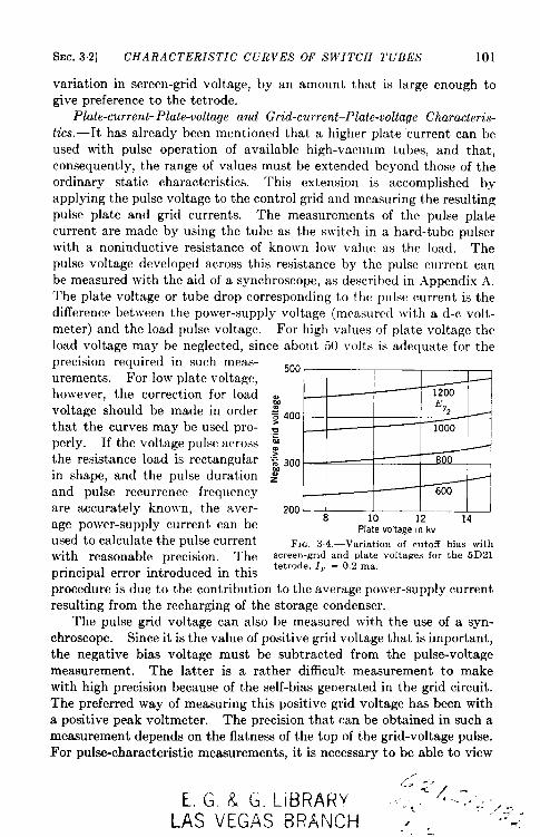
SEC. 32] CHARACTERISTIC CURVES OF SWITCIf TUBES 101
variation in screen-grid voltage, by an amount that is large enough togive preference to the tetrode.
Plate-current–Plate-voltage and Grid-current–Plate-voltage Characteris-
tics.—rt has already been mentioned that a higher plate current can beused with pulse operation of available high-vacuum tubes, and that,consequently, the range of values must be extended beyond those of theordinary static characteristics. This extension is accomplished byapplying the pulse voltage to the control grid and measuring the resultingpulse plate and grid currents. The measurements of the pulse platecurrent are made by using the tube as the sivitch in a hard-tube pulserwith a noninductive resistance of known low value as the load. Thepulse voltage developed across this resistance by the pulse clu-rent canbe measured with the aid of a synchroscope, as descrilml in .{ppendix .~.The plate voltage or tube drop corresponding to the pulse current is thedifference between the power-supply voltage (measured ~vith a d-c volt-meter) and the load pulse voltage. For high values of plate voltage theload voltage may be neglected, since about 50 volts is adequate for theprecision required in such meas-urements. For low plate voltage,however, the correction for loadvoltage should be made in orderthat the curves may be used pro-perly. If the voltage pulse acrossthe resistance load is rectangularin shape, and the pulse durationand pulse recurrence frequencyare accurately knowm, the aver-age power-supply current can beused to calculate the pulse currentwith reasonable precision. Theprincipal error introduced in this
500
1200&
~E
f 400 92 +—
‘0 1000 I&?“%300 —- — 800~z /
— --%i--?
Plate voltage in kv
FIG. 3.4.—Variation of cutoff bias withscreen-grid and plate voltages for the 5D21tetrode, 1P = 0.2 ma,
procedure is due to the contribution to the average power-supply currentresulting from the recharging of the storage condenser.
The pulse grid voltage can also be measured with the use of a syn-chroscope. Since it is the value of positive grid voltage that is important,the negative bias voltage must be subtracted from the pulse-voltagemeasurement. The latter is a rather difficult measurement to makewith high precision because of the self-bias generated in the grid circuit.The preferred way of measuring this positive grid voltage has been witha positive peak voltmeter. The precision that can be obtained in such ameasurement depends on the flatness of the top of the grid-voltage pulse.For pulse-characteristic measurements, it is necewary to be able to view
d“’*(. -L G, & (-i.LIBRARY -.<- --, :,/:.; -,
LAS VEGAS i3F?ANCH -~, > ‘--;

102 VACUUM TUBES AS SWITCHES [SEC.3.2
the grid pulse on a synchroscope in order to make the top of the pulse asflat as possible. If a spike is present on the top of the pulse, the peak-voltmeter reading may correspond to the spike maximum, thus giving anerroneous reading of the positive grid voltage. The pulse grid current isdifficult to measure, and has usually been obtained from the average gridcurrent and the measured duty ratio. Although this procedure is lack-ing in precision, it has been adequate for pulser applications in micro-wave-radar systems.
In order to obtain the data necessary for the pulse characteristics ofsmall tubes of the receiver type, a circuit was devised which made itpossible to read pulse voltages and currents directly on ordinary d-cmeters. i This circuit uses pulse voltmeters to measure pulse voltages,and the pulse currents are obtained by measuring the pulse ~roltages acrossprecision noninductive resistors connected in series with the grids andthe plate of the tube under test. A block diagram of this circuit is shownin Fig. 3.5, and a schematic diagram in Fig, 3.6.
Pulse in
!Variable Tube vfpb~
bias * undersupply test voltage
R9 RP supply1, I
1 1 T f
rPeak Peak Peek
Peak 19 detector detector detector—
detector—
meter and and andeg meter 1P meter eP meter
FIG, 35.-Block diagram of a circuit used to determine the pulse characteristics of a tubaof the receiver type.
The pulse characteristics for several tubes are shown in Figs. 3.7-3.11.From curves such as these, the effective resistance of the tube and thegrid-driving power can easily be determined for the pulse current cor-responding to the pulser output power. One of the first hard-tubepulsers to be used extensively in a microwave-radar system used twoEimac 304TH tubes in parallel as the switch. A pulse-power outputof about 150 kw with a pulse voltage of 12 to 13 kv was required for this
1R. B. Woodbury, “ Pulse Characteriaticaof Common Receiver Type Tubea,”RL Report No. 704, Apr. 30, 1945.

SE
C.32]
CH
AR
AC
TE
RIS
TIC
!C
UR
VE
SO
FS
WIT
CH
TU
BE
S
II

104 V.4CC”L-JIT1’BES AS SJI’ITCHES [SEC.3.2
pulser. The 304TH \~asfound to \rithstand the high plate voltage dur-ing the intcrpldsc interval. The curves of Fig. 3.7 indicate the reasonthat t]VOt~lbes in pamllel \vereneeded to carry the pulse current. From
E%+
— 1200W1000v800V
L
1 2 3 4Platevoltagein kv
(a) 5D21 (\YE) and 715B (if-E and l{ay -theon), EC = +200 volts
30
EE
m I%
c“= +200 v: 20k.:.-
! 10
;~a +200 v
o0 1 2 3 4
Platevoltagein kv
(b) .51)’21 (\\-E) anti 71,5B (\\”E and nay -theoll), E<,. = 1?00 .-oIts
g 20mc
m
Eg,.-E +:> 10 E91=2wv
+400v
+V;&
I 1P +100vv
91:()go 1 2“3 4: Platevoltagem kv
(c) 304TH (Ei,nac),F~~. 3 7.—Pulse-characteristic curves
for the 5D21 and 715B tetrodes and the304TH triode.
these curves it is seen that a posi-tive grid drive in excess of 400 voltsis required to obtain a pulse platecurrent of 12 amp, and that, underthese conditions, it is necessary tooperate the tube ~vith a tube dropof 4 to 5 kv. For t!ro tubes inparallel, however, the required pulseplate current can be obtained witha positive grid drive of about 200volts and a tube drop of about 2kv. The low grid-driving polrernecessary to operate the 304TH asthe pulser switch tube ~vasan addi-tional reason for its selection. Oneof the most undesirable features isthe high cathode-heating powerrequired, 125 watts for each of thetwo tubes.
After the 715B tube was devel-oped by the Bell Telephone Labora-tories, it was possible to constructa hard-tube pulser for 150-kw poweroutput with a higher over-all effi-ciency and more satisfactory pulseroperation. The curves for this tubeare shown in Fig. 3.7, where it canbe seen that a pulse current of 15amp can be obtained with a tubedrop of about 1.5 kv and a positivegrid drive of 200 volts. In thiscase also, the grid-driving power issmall because a grid current of lessthan 1 amp is necessary. Sincethe cathode-heating power for the715B is 56 watts, a saving of
about 200 watts is effected when this tube is used in preference totlro 304TH tubes. Also, slightly less power is dissipated in thei 15B tube than in two 304TH tubes because of the lower tube drop.The power dissipation resulting from the screen-grid current is not suf-

SEC. 32] CHARACTERISTIC CURVES OF SWITCH TUBES 105
ficient to offset the decrease in plate dissipation. The screen-grid volt-age, required because the 715B is a tetrode, can generally be obtainedfrom the power supply for the driver circuit, and the pulser design is notfurther complicated.
In addition to the positive grid drive and the tube drop necessary inorder to obtain a given value of plate current, the shape and dispositionof the characteristic curves as a function of grid voltage are also important
Platevoltagein volts
(a) E,, = +200 ,mlts
e Eg,..5~.lo /~ov~lJ5 \,/
%~:
00 400 800 1200 1600
Plate voltagein volts(b) E,, = S00 volts
FIG. 3S.-Pulae-characteristic curvesfor the two sections of the S29 beam tetrode(RCA, NU, Kenrad, Raytheon).
I
400 800 1200 1600Plate voltage in volts
(a) E,, = + 200 Volts
400 800 1200 1600Plate voltage in volts
(b) E,, = Soo voltsFIG. 39,-Pulse-characteristic ~“rve,q for
the 3D21 beam tetrode (Hytron).
to pulser operation. The effect of variation in grid voltage on the outputpulse of the pulser may be illustrated by dra~ving the load line on theplate-current–plate-voltage diagram. In Fig. 3.12 a family of character-istic curves is drawn for a tetrode such as the 715B for constant screen-grid voltage. Two load lines are drawn on this diagram. Line (1)corresponds to a low-resistance load in series with a bias voltage, such asthe dynamic resistance of a magnetron or biased diode, line (2) corre-sponds to a high-resistance load of the same magnitude as the staticresistance of the biased diode for the operating point Op. From thisdiagram it is evident that a change in grid voltage corresponding to the

106 VACUUM TUBES AS SWITCHES [SEC. 3.2
curves A, B, and C has a negligible effect on the operating point for theswitch tube. The only change in the operating point is due to the slightshift of the curves toward lower plate voltage as the grid voltage is low-ered. This effect is observable in the tetrode characteristics shown inF&. 3.7, 3.8, and 3.9, and is caused by the smaller grid currents thatcorrespond to the lower values of positive grid drive. The load voltage
; soc.-Ee 20
kiiiizl
Eg,=+1500N5“ ~g,=+looo~~ 1PM10~ 192 Eg,=+1500v; J9,o??0 12345
Platevoltagein kv
(a) 6J121 (Raytheon), ,??02= 2kv.
:30c.-; Z.
m
Eg,=+1500v
k2 Eg,=+ 1000 v“: 10 1P
v 19,. .EO=+1501)V;0so 12345a Plate voltage in kv -
3Em
E9, = +150V.E:2 /~
:.=
%’1~~
200 100 200 300 400
Plate voltage in volts(a) 6SN7 (both sections).
120-
E Eg, = +2kvm.s 4z 80 /: IP~ E9, = +1 kv~ \
~Eol = +2 kvb
~ 40Ig1<\
;~ Eg, = +1 kv
‘o1 2 3 4 5
Platevoltagein kv(b) 6C21 (Eimac, Westinghouse, GE, (b) 527 (Eimac).
Machlett). FIG. 3.11 ,—Pulse-characteristic curves forFIG. 3. 10,—Pulse-characteristic curves for the 6SN7 and 527 triodes.
the 6D21 tetrode and the 6C21 triode.
and the load current therefore remain very nearly constant even thoughthe grid voltage may change within this range during the pulse. There-fore, if adequate positive grid drive is provided to keep the operatingpoint for the tube somewhat below the knee of the characteristic curve,irregularities in the top of the grid voltage pulse are not observed on thepulser output pulse. This consideration is of considerable importance tothe design of the driver circuit.
If the initial operating point corresponds to the curve C of Fig. 3.12and the grid voltage changes over the range C to E, a different situationobtains. In this case both the load voltage and the load current are

SEC. 3.2] CHARACTERISTIC CURVES OF SWITCH TUBES 107
affected. For the low-resistance load the change in voltage is AV, andthe change in current AI,. Similarly, for the high-resistance load thecorresponding changes are AVt and A12. Because of the slight upwardslope of the characteristic curves abcve the knee, the change in current isgreater for the low-resistance load and the change in voltage is less.When the pulser switch tube is operated in this manner, irregularities inthe grid-voltage pulse are transferred to the load pulse.
When the characteristic curve of the switch tube does not have aknee as shown in Fig. 312, the shape of the grid-voltage pulse must becontrolled more carefully in order to obtain a flat-topped pulse at the
A
B
c
AVI -i +- 1~Av2-1
v’ —
FIG,3,12.—Family of plate-current-plate-voltage curves with load lines correspondingto a low and a high resistance showing the effect of a change in grid voltage on the operatingpoint of a pulser switch tube; A, B, C, D, and E are curves for different values of Eg, withE,, = constant.
load. As an example, see the curves for the 304TH tube in Fig. 3.7.There are triodes that exhibit a knee in the characteristic, as shown bythe curves for the 6C21 and the 527 in Figs. 3.10 and 311. If thesecurves are compared with those for the tetrodes in Figs. 37, 3.8, and3.9, however, it is seen that the curves for different grid voltages areseparated by a greater amount below the knee. The change in theoperating point that results from a change in grid voltage is not as greatas that resulting from operation above the knee of the characteristiccurve. For a 6D21 tetrode this knee occurs at such a low current thatthe tube is usually operated well above the knee. Because of the greaterslope of the upper portion of the curves for this tube, the variation ingrid voltage does not have as great an effect as it does for comparableoperation of the 6C21 triode.
A comparison of the curves for the 6C21 and the 6D21 in Fig. 3“10
108 VACUUM TUBES AS SWITCHES [SEC. 33
with the curves for the 5D21 and 715B in Fig. 3.11 indicates that thelatter tubes are better from the standpoint of plate current and grid-driving power. The only reason for using a 6C21 or a 6D21 as a pulserswitch tube is the fact that they can stand a higher plate voltage thancan the 5D21 or 715B. This comparison illustrates the increased dif-ficulty involved in designing a hard-tube pulser for a power-supplyvoltage in excess of 20 kv with existing high-vacuum tubes. liThen pulsepower of the oricr of magnitude of several megawatts is wanted, how-ever, this disadvantage must be accepted until better tubes are available.A 1-.Mw hard-tube pulser using three of the 6C21 tubes in parallel asthe switch has been built and used extensively. This pulser has a pulseoutput of 25 kv at 40 amp. The 6D21 was used in a pulser designed tohave an output of 3 Mw, 30 kv at 100 amp. In this case five tubes wereused in parallel. The highest power hard-tube pulser built at the Radia-tion Laboratory used six 527 tubes as the switch. This pulser had anoutput of about 25 kv at 400 amp, and a grid-driving power of about, 700kw.
An effect similar to that resulting from variation in grid voltage isobserved if the screen-grid voltage of a tetrode is allowed to change. Theeffect is illustrated by the family of curves for the tetrodes in Figs. 3.7,3.8, and 3.9 in which the control-grid voltage is constant and the screen-grid voltage is varied. For satisfactory operation of a tet rode as theswitch tube, therefore, the voltage of the screen grid must not be allowedto change during the pulse. Because of the flow of pulse current to thescreen grid and the plate-to-screen capacitance, it is necessary to providea large bypass condenser between the screen grid and the cathode. Formost effective operation, this condenser must be connected as close tothe tube clement as possible.
The curves for the 829 beam tetrode shown in Fig. 3.8 illustrateanother consideration in the operation of a tetrode as the switch tube.For a given pulse plate current and tube drop it is advantageous to usethe highest possible screen-grid voltage and the lowest possible positivegrid drive. The curves of Fig. 3.8 indicate that the control-grid currentdecreases as the screen-grid voltage is increased for a gi~’en positive grid-drive voltage. Since the screen-grid current increases with the screen-grid voltage, some compromise must usually be made between the twogrid voltages for most efficient tube operation.
The shape of the characteristic curves has another effect on pulseroperation. If the grid \-oltages are held constant, there is still the pos-sibility of changing the operating conditions by varying the power-supplyvoltage. This effect is discussed in detail in the follotving section.
3.3. The Effect of Switch-tube and Load Characteristics on the PulserRegulation.-The characteristics of the switch tube in a hard-tube pulser

SEC. 3.3] EFFECT OF Sli-I TCH AA’D LOA.!) ON REGULATION 109
may be utilized to a certain extent to minimize the change in load cur-rent resulting from :1 change in the power-supply voltage. This po\ver-supply voltage may vary because of changes in either the input voltageto the pulser or thc a~’erage current from the po\ver supply. The changein a~~eragrcurrent may be brollght about by variations in the duty ratiothat occur as a result of changes in either the pulse duration or the pulserecurrence frcq~lenry. The discussion of this section sho~vs the \vay in\vhich this regulation depends on the characteristics of the load and thes\vitch tllt~e.
Those features of a hard-tube pulser that are essential in this discus-sion arc showm sc]mmat ically in Fig. 3.13. In this circuit ~= and rPrepresent the s\ritch tube, Ebb is the po\ver supply, R. is the isolating
Cw
I
r~z
t
p%
1P
IPoK
‘r———— _______----1_—- ;
II
//JSil
o ~, v vp-1VpP2
~-lG. 313-Equiv:dcnt r]rruit of a hard-tube pulser with a biased-diode load.
I:IG. 3.14.—Currcnt-voltage characteristicof a high-vacuum switch tube.
resistor, CWis the storage condenser, Z, is the condenser-recharging paththat is necessary \vhen the load is unidirectional, and r-l, S1, and V,represent the load, The considerations are restricted to the voltages andcurrents that correspond to the top of a pulse when the pulsing is con-tinuous, and to pulse durations that are considered small compared withthe interpulse interval.
The plate-current-plate-voltage characteristic of the svitch tube maybe represented as sho~vn in Fig. 3.14. For the purposes of the presentdiscussion, the lP-VP curve is very nearly a straight line above somecurrent value Z~,, and for the greater part of the curve belo\v some cur-rent lP,. The knee of such a curve, already referred to in the precedingsect ion, is the region bet \vecn 1,, and In,. TN-Otube resistances may bedefined, one for the operation of the switch tube below the knee, and theother for the operation above the knee, Thus
and
1
– (-)
d v,,‘“=tanb= dI,, 1,<1,,
(1)
(2)

110 VACUUM TUBES AS SWITCHES [SEC. 3.3
For a tetrode, two families of characteristic curves may be drawn,one for Eg, constant and the other for EO, constant. It is evident fromthe tetrode curves shown in Figs. 37, 3“8, and 3.9 that the values ofr-~for various values of the grid voltages are essentially the same. Thevalue of r~, however, does change somewhat with variations in either ofthe grid voltages. The change is small, and is neglected in this discus-
(a) E,, constant, (b) Eo, constant.FIG. 3.15.—Idealized current-voltage characteristics of a tetrode.
sion. Theidealized curves foratetrode aresketched in Fig. 3.15. Thecurves of Fig. 3.15a may also be considered applicable to a triode. Thevalue of rPis more dependent on Eu, in a triode than it is in a tetrode, butthe characteristic curves shown in Figs. 3.10 and 3.11 indicate that r; ispractically independent of E,,.
The most general load that can be considered is one having a non-linear current-voltage characteristic as sketched in Fig. 3.16. The
magnetron or biased-diode load dis-
t
/ cussed in Chap. 2 is a special case ofthe nonlinear load in which the current
1~ I below V. is considered negligibly smalland the 1-V curve above V, is linear.
0/ Compare Fig. 3.16 with Fig. 2.11. In
// discussing the effect of the load charac-
// teristics on the pulser regulation, it isnot necessary to restrict the argument
v’to this special case since only the
II ~ values of V1 and Z1 at the top of theFIG. 3.16.—Current-voltagecharacter-
isticof a nonlinearload. pulse are being considered. It is as-sumed, however, that the range of
voltage and current values is so small that the Z-1’ curve may be con-sidered linear at the operating point.
The static resistance of the load is given by
RZ=J; =&fi
and the dynamic resistance is
(3)
SEC. 3.3] EFFECT OF SWITCH AND LOAD ON REGULATION 111
(4)
For a small range of values about a particular operating point, the follow-ing relationships hold approximately:
VI = v. + Tlrt (5)and
VI – v,11 = y. (6)
By using the above relations for the switch-tube and load char-acteristics, and referring to the pulser circuit of Fig. 3“13, it is pos-sible to derive the relationships that express the load operating voltageand current in terms of these characteristics and the circuit parameters.In particular, there are two operating conditions for the switch tube tobe considered, namely, (1) operation above the knee of its characteristiccurve corresponding to the point marked A in Fig. 3“15 (type A opem-tion), and (2) operation below the knee corresponding to the point Bindicated in Fig. 3.15 (type B operation).
Operation of the Switch Tube above the Knee of the l,-VP Curve.—Asstated previously, the power-supply voltage Ew varies principally becauseof changes in line voltage and duty ratio. Variation of the line-voltageinput to the pulser causes a change in all the voltages in the pulser, andtherefore changes the voltages applied to the grids as well as the platevoltage of the switch tube. As indicated in Fig. 3.15 changes in the gridvoltages cause the value of the intercept 1~, indicated in Fig. 3.14, tochange. Therefore, in considering the effect of line-voltage changes onthe operating conditions for the load, the variation in Z~ must also betaken into account. The change in operating values for the load andswitch tube that results from the simultaneous variation of Ew andIL may be written as follows:
(7)
(8)
(9)
Referring to Fig. 3.14 and the definition of r; given by Eq. (2) theplate current for the switch tube is given by
(lo)

112 VACUUM TUBES AS SWITCHES [SEC.3.3
Considering the pulser circuit of Fig. 3.13, the plate current is
1, =11+1.+1,. (11)
As discussed in Chap. 2, the voltage across the condenser, VW,is neververy different from EM if the capacitance is sufficiently large. For steadypulsing the condenser voltage is slightly less than the power-supplyvoltage, but for the purpose of this discussion it is reasonable to neglect
this difference and to assume that Vw = EW The voltage across theload with switches ST and St closed is, therefore,
The currents Z, and I. in Eq. (11) can be expressed in terms of Vl, thus,
(13)
where Z, is the effective impedance of the condenser-recharging path.Also
I= E&–vP =;,c
R. c(14)
Thus from Eqs. (6), (10), (11), (12), (13), and (14), the expression for theload current becomes
From Eqs. (6) and (15),
(16)
From Eqs. (12) and (16),
It is seen from Eqs. (7) and (15) that the variation of load current canbe made zero if
The characteristic curves for tetrodes shown in Figk 3“7, 3“8, and 3“9and sketched in Fig. 315 indicate that it is possible to satisfy this rela-

6EC. 3.3] EFFECT OF SWITCH AND LOAD ON REGULATION 113
tion. For a particular tetrode and for moderate changes in grid voltages,the following relations are approximately true:
dI~ = (kldEO,) E,,comt, (19)and
dI; = (k,dll,,)~,,cn~,. (20)
If the characteristic curves for the switch tube are known and the valuesof kl and kz therefore determined, it is possible to devise a control circuitthat changes the grid voltages, as EM varies, in such a way as to satisfyEq. (18). Since the voltage outputs of the grid and plate power suppliesmay depend on the input line voltage to approximately the same degreesuch a control circuit should not be very complicated if the duty ratioremains constant. When the duty ratio changes, however, the averagecurrents also change, and the added factor of inherent regulation in thesepower supplies has to be considered, which complicates the design of thecontrol circuit considerably.
For a low-power pulser using a tetrode switch tube, grid voltages ofonly a few hundred volts are generally required. Power supplies thatare electronically regulated against variations in input voltage and outputcurrent can easily be built for these voltages. It is not economical,however, to construct a high-voltage power supply with similar regula-tion. The changes in load and switch-tube operating values thatare due to variations in the high-voltage power supply only may beobtained from Eqs. (15), (16), and (17) by differentiating withrespect to EM. Since the denominator of each of these expressions is thesame, let
i)=rl+ r;+*+*.c *
Then
(21)
aI1 1Z=D’ (22)
a vl _ nd& – ~’ (23)
and+-. ‘
av.~:+ L-+Ql
R, Z,
dEti = D(24)
D–rl——D“
(25)
The Eqs. (15), (16), and (17) do not explicitly involve time. Ifthe condenser-recharging path 2, is an inductive resistor, however, the

114 VACUUM TUBES AS SWITCHES [SEC. 3.3
time measured from the start of the pulse is included because, for thiscase,
z.= “R,1 _ ~-tit
where R, is the resistance and L. is the inductance of the element. Threecases are of interest in this connection:
1. When the recharging path is a wire-wound resistor whose induct-ance is not negligible. In general, L,/R, <<t where & = , (thepulse duration), so Z. = R,.
2. When the recharging path is an inductance coil of low ohmicR.t
resistance such that L,/R .>> t where t- = r. Expanding e-~and using only the first two terms, Z, z L,/t.
3. When the recharging path is a combination of inductance andresistance for which L./R, = T. If, for a particular value of r,L,/R, = T, then Z, = R#3.63.
When the recharging path is an inductance having low resistanceCondition 2 obtains, and the load current decreases during the pulse, as isevident from Eq. (15) in which the term r~,fZ, increases with time. Forlong pulses, that is, with a duration of 2 psec or more, this effect maybecome prominent. This decrease in load current during the pulseoccurs in addition to the change in load current given by Eq. (22).Other effects already discussed, such as the drop in voltage across thestorage conaenser and the possible change in cathode emission in theswitch tube, can also cause the load current to change during a pulse.
Operation oj the Switch Tube below the Knee of the lP-VP Curve.—Theswitch tube is now operated at point (B) indicated in Fig. 3.15. IfFig. 314 is again referred to, it is evident that the relationships derivedabove also apply to this case, when rP is substituted for r; and Iw is sub-stituted for Z~. The value of 1,0 may be expressed in terms of V@, thus
With these changes, the Eqs. (15), (16), and (17) become
(26)
(27)
(28)

SEC. 3.3] EFFECT OF SWITCH AND LOAD ON REQULA TION 115
and
In general, Vw is so small compared with EM that it may be neglected.When the switch tube is operated below the knee of the lP-VP charac-
teristic curve, it is evident that changes in line-voltage input to the pulseraffect the operating values for the load only because of the resultingchange in the power-supply voltage, since all the terms in Eqs. (27),(28), and (29) except EM are independent of the pulser input voltage.The pulser regulation is therefore obtained simply by differentiating theseequations with respect to EN without considering the variation of gridvoltages. The resulting expressions are identical with Eqs. (22) to (25)when rP is replaced by r;.
Examples of the Two Types of Switch-tube OperaLion.—The order ofmagnitude of the effect of variations in the high-voltage power supplyon the operating values for the load and switch tube is illustrated by thefollowing typical values for two pulser-load combinations. As anexample of a medium-power combination, the operation of a pulser isconsidered with a 715B switch tube and a 725A magnetron as the load.The 2J41 magnetron operated with a pulser using a 3D21 switch tube is anexample of a low-power combination. Data are given for the two typesof switch-tube operation in each case. The term “type A operation”refers to operation of the switch tube above the knee of the l~-VP curve,and the term “type B operation” refers to operation below the knee ofthe curve.
For type A operation of the715B tube, the applied screen-grid voltageis about 1000 volts, and the positive grid drive must be about 100 voltsin order to obtain a current of 10 amp through the 725A magnetron.With a magnetic field Gf about 5000 gauss the voltage across this magne-tron is approximately 11 kv for a 10-amp current pulse. In order toobtain the same operating conditions for the magnetron with type Boperation of the 715B, the screen-grid and control-grid voltages must beraised to about 1200 volts and 150 to 200 volts res~ctivelv.
The normal operating voltage and current for a 2J41 magnetron areabout 2.5 kv and 1 amp. The 3D21 switch tube in a pulser operatingwith this magnetron requires about 300 volts on the screen grid and a25-volt positive grid drive for type A operation. For type B operationof the 3D21, these grid voltages must be increased to about 400 voltsand 50 volts respectively.
Values of pulser and switch-tube parameters considered typical for

116 VACUUM TUBES AS SWITCHES [SEC.8.8
the above-stated operating conditions are given in Table 3“2. Thevalues of the quantities dIJdE~, dVJdEt,t,, and dVP/dEti that havebeen calculated from these data and from Eqs. (22), (23), and (25) arealso tabulated. It is to be noted that the quantities r~ri/R~ and r~rl/Z,may be neglected for all practical purposes, since their sum is only oneor two per cent of the sum (TP+ n). A negligible error would thereforehave been introduced for these examples if the switch-tube current had
TARLE 3.2-VALUES CALCULATED FRO?dEQS. (22), (23), AND(25) FORTYPICALOFERATINGCONDITIONSFORTwo PULSER-LOADCOIABINATIONS
715Bswitch tube, 725Amagnetron, 3D21 switch tube, 2J41 magnetron
type A operation type B operation type A operation type B operation
10,000 ohms
(1) 10 mh
10,000 ohms 15,000 ohms 15,000 ohms
(1) 10 mh 15,000 ohms +5 mh
15,000ohms +5mh
15,000 ohms +5 mh
15,000 ohms +
5 mh
z.(2) (7500 ohms +
3 mh)
(2) (7500 ohms -t3 mh)
2500 ohms . . . . . . 30730 ohms
100 ohms. . .
125 ohms 125 ohms 200 ohms
,. ...,, ... ,.. .
75 ohms
20G ohmsrl
31 ohmsI
............ 47 ohms . . . . . . . . . . . . .
for t = 10-s sec(1) 31 ohms(2) 46 ohms
for t = 10-6 sec44 ohms
r&z,
. . . . . . . . . . . . . . .
TPT1
R.1.250hms 1 ohm
—for t = 10-6 sec
,, . . . . . . . . . . (1) 1.25 ohms . . . . . . . . . . . .(2) 1.5 ohms
for t = 10-6 sec1 ohm
3.7 x 10-’ ~ 4.4 x 10-’* 2.6 X 10-’ ~ 3.6 X 10⁻³ ~
0.047 0.55
0.95 0.45
0.052 0.72
0.280.95

SEC.33] EFFECT OF ,S1l’ITCff .4.VD LO.4D ON REGCL.-l TIO.V 117
been assumwl to ~Je equal to the load current. It is rdso evident that,for the type A opertition of the sjvitch tube, the value of r-lmay also beneglecte(l in the ckmominat or of the expressions (22), (23), and (25) with-out causing serious error in the calculated pulscr regulation.
These examples indicate that the change of load current that is dueto the variation of the high-voltage supply is decreased by a factor ofabout 10 if the sivitch tube is operated above rather than beloiv the kneeof the lP-V,, characteristic. It must be remembered, ho\vever, that inorclcr to realize this gain, the screen-grid voltage and the positive griddrive must not be allouwl to change. .1s pointed out in the previoussection, \rhen the load line crosses the slritch-tube characteristic above theknee, the shape of the control-grid volttige pulse is transferred to the loadpulse. In order to take a(lvantage of the bettrr regulation against po\ver-supply variations, and thus to realize an outpllt-pulse amplitude thatis constant throughout the p(lkc t!llration, the control-grid pulse musthave a flat top. The partic~llar applictition to which a pulser is to beadapted generally determines the type of siritch-tube operation that isdesirable.
Some pulser applicat i(ms reqllire that the opcrat ing conditions forthe 10:u1must not clamgc even t llo~lgll thr duty ratio may vary over widelimits. For such a p~llser, eitlwr the high-voltage power supply mustI)e regulat [’d for a Iargc lariat ion in the average current delivered, orthe reg(llation must IN ol)tained by type .i operation of the s\ritch tube,in Irhich case the voltage ucross The slritch tube changes by almost thesarnc zrnmmt as the po\rer-supply yoltage. It is therefore necessaryto adjust tllc pulscr VOlt:lgCS so th:lt the lolvest value of EM to be expectedin the operation does not, ca(ise the tube drop, V=) to fall below the valueV=, indicated in l~ig. 3.14.
For a pulser designed to operate at constant duty ratio, the variationin polver-supply \-oltzge produced by the change in a}rerage current isless important than that caused by changes in the line voltage. It mustbe decided, therefore, \vhether or not the improved regulation providedby type A operation of the stvitch tube compensates for the difficultyof regulating the grid-voltage polvcr supplies. If the effect of line-volt-age variation is not serious, there are some advantages to be gained byoperating the switch tube belo\v the knre of the lP-VP curve. Besidesthe smaller effect of change in grid voltage mentioned in the previoussection, there is also the a(l]antagc that a lo\rer poirer-supp]y voltage isrequired, as can be seen from the relative positions of points .4 and B inFig. 3.15.
N’hen the load has a dynamic resistance that is 10JVcompared \vith itsstatic resistance, the variation of load current is generally of more interestthan the variation of load voltage. (In the operation of a magnetron the

118 VACUUM TUBES AS SWITCHES [SEC. 3.3
oscillation frequency is a function of the magnetron current. The changeof frequency, f, caused by current change is referred to as the “pushingfigure” of the magnetron, and is generally expressed as the value ofd~/6’Z., where 1- is the magnetron current.) For a magnetron load, theratio dZJIl is often more significant than the value of dI1. From the equa-tions developed in the preceding discussions it is possible to expressthe ratio dZt/Zl in terms of the ratio dEw/E~. Thus Eq. (22) gives
(22)
Dividing by the value of 11 given by Eq. (27) for type B operation,
For type B operation of the 715B switch tube, a 725A magnetron operat-ing at 11 kv and 10 amp, and the data given in Table 3.2,
v. = 9750 voltsand
Ebb = 12 kv.
With these data, Eq. (30) gives
This value is the same as that obtained in Sec. 2“8 by the use of Eq.(2. 106) assuming that n = r.. Thus, the variation in load current leadsto very nearly the same regulation factor as the variation in load powerwhen the dynamic resistance of the load is small.
If the high-voltage power supply has very good regulation, the per-centage change in the input line voltage and in the power-supply voltageis almost the same. The percentage change in load current is thereforeabout six times the percentage change in input line voltage for an averagemagnetron load. For a pure-resistance load, 1’. = O, and the percentagechange in load current is equal to the percentage change in input linevolt age.

CHAPTER 4
DRIVER CIRCUITS
BY G. N. GLASOE
In the preceding discussion of the hard-tube pulser circuit, it isassumed that there is an available means of making the switch tube con-ducting for a controlled length of time that corresponds to the desiredpulse duration. The control of the pulse duration can be accomplishedby the application of the proper voltage to the grid of a high-vacuum tube.The circuit that performs this function is called the “driver,” and is anessential part of a hard-tube pulser.
In the discussion of switch-tube characteristics in Chap. 3 it is pointedout that, in order to obtain the necessary plate current, the grid of theswitch tube must be at a positive potential relative to the cathode duringthe pulse. Since this grid must be maintained at a high negative voltageduring the interpulse intervals, the output voltage of the driver mustequal the sum of the bias and positive grid-drive voltages. This requiredvoltage out put is called the “grid swing, ” and may vary from about ahundred volts to several kilovolts depending on the switch-tube charac-teristics. The pulse-power output of the driver is, therefore, the product
of this grid swing and the grid current in the switch tube. For very highpower pulsers, for example, the one using six 527 tubes in parallel men-tioned in Sec. 3“2, the driver output power may amount to as much asten per cent of the pulser output power. In general, however, it is morenearly of the order of magnitude of one per cent of the pulser outputpower.
The pulse duration is entirely determined by the characteristics ofthe driver circuit for a hard-tube pulser. The circuit should, therefore,be designed so that all the pulses, in a long succession, are identical, andtheir duration can be determined accurately. For such a succession ofpulses, it is generally desired that the interpulse intervals, as well as thepulses, be of controlled duration. The control of the interpulse intervalsis usually accomplished by constructing the driver circuit in such a waythat it does not produce an output pulse until it has received the properimpulse at its input terminals. These impulses are called trigger pulses,and are produced by some form of auxiliary timing circuit that has anegligible power output. In order to keep the pulser design as versatileas possible, this trigger generator is ordinarily not a part of the pulser,
119

120 DRIVER CIRCUITS [SEC.4-1
and is commonly used for other functions in addition to starting the actionof the driver. One of the principal advantages of the hard-tube pulserover the line-type pulser is that the pulse duration is determined in arelatively low power circuit. For this reason, the driver circuit canbe designed so that the pulse duration and the interpulse interval maybe changed readily over a wide range of values without necessitating anymajor changes in the circuit. A given design of a hard-tube pulser maytherefore be adapted to a large variety of applications with little dif-ficulty; therefore, a pulser of this type is particularly suitable for researchand development work where the specific values of pulse duration,interpulse interval, and output power desired are not definitely known.
There is an inevitable time delay between the start of a trigger impulseand the start of the pulse at the pulser load. When this time delay variesin a random manner from pulse to pulse, there is said to be (‘time jitter”in the output pulses. This time jitter causes unsatisfactory operationwhen the functioning of auxiliary circuits depends on both the triggerimpulses and the pulser output pulses.
4.1. The Bootstrap Driver.-Many circuits that are available forgenerating voltage pulses are incapable of delivering enough power todrive the grid of a pulser switch tube. The obvious procedure is there-
TInput-pulse
I, ,++
+
---
I “;i~ ,“plJ,pu,,e> output> pulse
.1X—
h+---
n,,+”,!} 4+---
Input pulse
I I(a) (b) (c)
FIG. 4.1.—(a) Plate coupling; requires “ on” tube for a positive output pulse. (b)Cathode follower; requmes “‘ off’ tube for positive output pulse, voltage gain less than one.(c) “ Bootstrap” cathode follower; requires ‘‘ off” tube for positive output pulse, voltagegain greater than one
fore to design an amplifier with a power gain sufficient to deliver therequisite power. Several stages of amplification may be necessary, andthe problem of maintaining good pulse shape becomes rather serious.The sc+called “bootstrap driver” was devised to generate a pulse at alow-power level, and to amplify it with a minimum number of tubes andcircuit elements Although with the development of satisfactory pulse

SEC. 4.1] THE BOOTSTRAP DRIVER 121
transformers this circuit has become obsolete, it is discussed here becauseit was one of the first uses of the pulse-forming network as a means ofdetermining pulse duration.
Since the driver output pulse must be positive, the coupling to theplate of an amplifier tube, as indicated in Fig. 4.1, requires that the tubebe conducting during the mterpulse interval and nonconducting duringthe pulse interval. When it is considered that the output pulse mustsupply a current of the order of magnitude of several amperes to the gridof the switch tube, it IS obvious that such plate coupling is very wastefulof power. The cathode follower provides a means of getting a positiveoutput pulse with a normally “off” tube, as is indicated in Fig. 4.Ib.The disad~ antage of this arrangement is that the ratio of the voltageoutput to the voltage input is less than one. The arrangement of Fig.4. lc, however, provides both a voltage and a power gain greater thanone. However, the circuit generating the input pulse must be able torise or fall in potential as the potential of the cathode rises or falls as aresult of the flow of current in the cathode resistor.
ofr
FIG. 4.2.—Circu]t for a bootstrap driver.
The complete circuit of a bootstrap driver is shown in Fig. 4.2 Thepulse is generated in the part of the circuit that is enclosed in the dottedlines. This pulse generator is merely a low-power line-type pulser inwhich the pulse-forming network, PFN, determines the pulse duration(see Part II for the detailed discussion of line-type pulsers). The gase-ous-discharge tube Tz is the switch tube, and the resistance RZ, in parallelwith the input resistance of the amplifier tube T2, is the pulser load.

122 DRIVER CIRCUITS [SEC. 4.1
In the quiescent state of this driver circuit, the reference potential forall voltages is determined by the grid-bias voltage required for the switchtube in the pulser output circuit. In Fig. 4“2 this voltage is indicatedas (E.,).. Thus, the plate voltages for the two tubes are (E~)z and(J?i’b)S,and the grid voltages are (E.,)z and (E~,)s for tubes Tz and T,
respectively. The grid voltages are adjusted to be sufficiently negativeto keep the two tubes nonconducting. When tube T2 is nonconducting,the PFN is charged to a potential difference equal to (~b)2.
The operation of this circuit is initiated by applying a positive triggervoltage to the grid of Tz through the capacitance Cl and the diode T1.
When this grid is raised in potential relative to the cathode, the gas in thetube becomes conducting, and the PFN is connected directly across theresistance Rz. The point A is thus raised in potential relative to point B
by an amount depending on the characteristic impedance of the PFNand on the effective resistance between A and B. In general, an attemptis made to match these impedances so that one half of the network volt-age appears across Rz. By virtue of the coupling capacitance C’s, thegrid of Ts is raised in potential along with point A. The resistance Ramust be large enough to decouple the grid from the bias-voltage supplyduring the pulse. If the potential difference across R2 is greater than thebias voltage (Ec,)s, the grid of Ta becomes positive with respect to thecathode (point B in Fig. 4“2). Tube T3 is thus made conducting, and acurrent flows in the cathode resistance Rs. This current causes the pointB to rise in potential and, if the current is large enough, the grid of thepulser switch tube becomes sufficiently positive with respect to ground tomake the plate current sufficient to obtain the required pulser outputcurrent. It is to be observed that, as the point B starts to rise in potentialbecause of conduction in tube T,, all the parts of the pulse-generatingcircuit must also rise in potential. The circuit is referred to as a boot-strap driver, since it is raised in potential by its” bootstraps, ” so to speak.
The duration of the pulse from this circuit is determined by the timerequired for a voltage wave to travel down the PFN and return. Whenthis time has elapsed, the network is completely dischargecj (if the PFNimpedance is matched by the resistance between A and B), and
Ppotential difference across R, falls suddenly. This drop in potentialcuts off the current in both T3 and its cathode resistor, thus removing thegrid drive from the pulser switch tube.
The bootstrap action of this circuit has important consequences thatmust be taken into account in the design. When point B rises in poten-tial, it causes the cathode of the gaseous-discharge tube to rise with it;therefore, the life of this tube is seriously affected if the grid can notalso rise in potential. In order to permit the potential of the grid toincrease, the capacitance Cz, shown in Fig. 4“2, is added. The capaci-

SEC.4.1] THE BOOTSTRAP DRIVER 123
tance C, and diode T, are introduced todecouple effectively the grid ofTz from the trigger-pulse-generating circuit during this action. Thenetwork of resistances R 1 provides decoupling between the trigger inputand the bias supply, and allows the circuit to return to its quiescentstate during the interpulse interval. The resistance Rs provides decou-pling between the pulse-generating circuit and the power supply during thepulse. The value of this resistance should be as large as is possiblewithout seriously reducing the voltage on the PFN at the end of theinterpulse interval.
Another consequence of the bootstrap action is that the stray capaci-tance of the circuit to ground (wiring, components, filament transformers,etc.) must be kept as small as possible. As the circuit rises in potential,this stray capacitance must be charged, and, unless it is small, the pulseshape is seriously distorted. At the end of the pulse the charge on thisstray capacitance must leak off, and, as indicated in Chap. 2, if the RC
time constant for the discharge is large, the trailing edge of the pulse fallsslowly. In order to make the voltage drop more rapidly at the end ofthe pulse, the inductance L is introduced in parallel with the cathoderesistance R3.
This circuit was used successfully to drive the grids of two 304THtubes in parallel as the pulser switch tube. A bias voltage of about– 1000 volts and a positive grid drive of +300 to +400 volts were neces-sary. Thus, the voltage developed across the cathode resistance R3
had to be about 1300 to 1400 volts. This voltage was obtained with(E,), equal to 1550 volts when an 829 beam tetrode was used as the tubeTa. The gaseous-discharge tube T2 was either an 884 or a 2050, theperformance of the latter being somewhat more satisfactory. The volt-age (E.,) Zfor either of these tubes was critical: if it were too large or toosmall, the tube would tend to remain conducting. The value of (E.,) Zusually had to be adjusted for the particular tube being used. For thisapplication, the circuit was designed to give three different pulse dura-tions, ~, 1, and 2 psec. By the use of a selecting switch, any one of threedifferent networks could be connected into the circuit. For the highrecurrence frequency (2000 pps) used with the shortest pulse, the PFN
“did not become charged to the full value of (Eb)z if R6 were very large.On the other hand, reducing Rb made it more difficult to prevent tube T2
from becoming continuously conducting. With careful adjustment ofthe circuit voltages and the values of the circuit elements, however, itwas possible to obtain satisfactory operation at 4000 pps. The particulargaseous-discharge tube to be used had to be selected carefully, since thelong deionization time for some tubes did not allow the charge on thePFN to accumulate fast enough to produce the full network voltagebefore the initiation of the next pulse. The values finally used were

124 DRIVER CIRCUITS [SEC.4.2
(E,), = 500 to 600 volts and Rb = 0.6 megohm. The characteristicimpedance of the PFN was about 1500 ohms, and Rz ranged from 1500to 2500 ohms. The other values of the circuit components were asfollows: Cl = 0.005 ~f, Cz = C~ = Ci = 0.01 pf, R, = 100,000 ohms,R8 = 1000 ohms, R, = 25,000 ohms, R6 = 30,000 ohms, L = 2.5 mh.
4.2. The Blocking Oscillator or Regenerative Driver.—With thedevelopment of transformers capable of passing pulses of short duration,it became possible to design a driver circuit using a single tube. A cir-cuit of this type was used extensively in pulsers with medium-poweroutput (150 to 250 kw) for airborne microwave-radar systems, andbecame known as the blocking-oscillator driver. This name was givento the circuit because of a similarity between it and the blocking oscil-lators used to produce pulses in television applications. The drivercircuit is not an oscillator in the same sense as the circuit used in tele-vision, and may more properly be referred to as a “regenerative pulsegenerator. ” This term is not exclusively distinctive, however, sincethere is a large class of circuits, such as the multivibrator for example,which could go by the same name. The particular type of circuit dis-cussed here is called a “regenerative driver” in an attempt to avoidconfusion with the circuit used in television.
There are two essential differences between the regenerative driverand the conventional blocking oscillator:
1. The regenerative driver can be kept in its quiescent state for anindefinite length of time, and starts its operating cycle only whenthe proper impulse is applied to the input terminals.
2. The output pulse is almost constant in amplitude throughout thepulse duration, as a result of the circuit and tube characteristics.
There is still a third difference that is not always essential, namely,that the pulse duration from a regenerative driver is usually determinedby a line-simulating network, whereas that from most blocking oscil-lators is determined by a parallel LC-combination.
A regenerative driver circuit arrangement which incorporates aniron-core pulse transformer together with a line-simulating network inthe grid circuit of a vacuum tube is shown schematically in Fig. 4.3.As discussed later, the range over which the pulse duration may bevaried, by changing the network parameters, depends on the pulse trans-former characteristics. Because of the line-simulating network, thecircuit has sometimes been referred to as a “line-controlled blockingoscillator. ” The triggering pulse for this circuit is introduced directlyonto the grid; this arrangement is called “parallel triggering” in contrastto the method of series triggering shown in the circuit of Fig. 4.4. Thelatter circuit has been widely used in pulsers for microwave-radar systems,

SEC. 4.2] THE REGENERATIVE DRIVER 125
and the regenerative feature is therefore discussed from the standpoint ofFig. 4.4 rather than the earlier arrangement of Fig. 4.3. The series-trig-gering arrangement proved to be somewhat more stable and less critical inregard to the values of circuit parameters than the parallel-triggeringcircuit.
~—--
n
126 DRIVER CIRCUITS [SEC.4.2
ally used for the trigger generator in order to ensure a relatively low effec-tive resistance. The voltage appearing across the PFN starts a voltagewave traveling toward the open end, where it is reflected and returnstoward the transformer end. When this cycle is completed the PFN isfully charged, and the potential of the grid of T, starts to fall abruptly.The plate current in the tube then begins to fall, reducing the voltageacross winding (1). This process results in a reduction in the voltageacross winding (3) that makes the grid still more negative, and causes aregenerative shutoff of the plate current. The voltage across the gridwinding then disappears, and the PFN discharges through the resistancesR, hnd Rz, driving the grid below cutoff. The bias voltage (EJ1,
keeps the tube nonconducting until the next trigger pulse starts anothercycle.
The above description of the action of a regenerative driver is veryqualitative. The analysis of the effect of transformer and tube character-istics on this circuit is extremely difficult. An approximate analysis hasbeen made with a simplified circuit for the effects introduced by the pulse-transformer parameters. This analysis is given in Sec. 14.2.
In the action of the regenerative-driver circuit a voltage is inducedacross the winding (2). This winding is connected between the biassupply and the grid of the pulser switch tube. In order for this circuit tofunction as the driver for the switch tube, the voltage appearing acrossthis transformer winding must be equal to the required grid swing. Theload introduced by the grid circuit of the switch tube has a stronginfluence on the flatness of the top of the voltage pulse appearing at thegrid. If the load on winding (2) is small, the voltage pulse generally hasoscillations of appreciable magnitude superimposed on its top. Since
FIQ. 4.5.—Voltage pulse at the grid of a715B tube obtained from a regenerativedriver using an 829 tube. Sweep speed:10 div. per psec; p61se amplitude: 1000 volts.
switch tubes of a given type varyconsiderably in their grid-voltage–grid-current characteristics, it issometimes necessary to introduceresistors across one or more of thetransformer windings to damp outthe oscillations. These oscilla-tions are the result of the inherentleakage inductance and distributedcapacitance of the transformer,and they may therefore be mini-mized to some extent by carefultransformer design. The oscillo-scope trace reproduced in Fig. 4.5
indicates the character of the pulse obtain~d at the grid of a 715B s~tchtube from a regenerative driver using an 829 beam tetrode.

SEC. 4.2] THE REGENERATIVE DRIVER 127
Both the maximum and the minimum pulse durations obtainablewith a given regenerative driver are dependent on the pulse-transformercharacteristics. The maximum is determined by the magnetizing cur-rent and core saturation. “When the magnetization of the transformercore approaches saturation, the magnetizing current increases veryrapidly, increasing the tube drop and thereby reducing the voltage acrosawinding (1), and hence across winding (3). This decrease in voltagecauses the regenerative shutoff to start before the PFN is fully charged.The pulse may be terminated by this same process, even if the transformercore does not become saturated, if the magnetizing current becomes toogreat. The minimum obtainable pulse duration is determined by theinherent inductance and capacitance of the circuit (including the trans-former), exclusive of the pulse-forming network. For intermediatevalues of pulse duration, the duration of the output pulse correspondsreasonably well with the calculated value based on the inductance andcapacitance of the network. Thus, if LN is the total inductance and CN
is the total capacitance of the network, the time required for a voltagewave to travel from one end to the other is dLNCN and the pulse duration~=zm.
It has been possible to design regenerative drivers in which the pulseduration may be varied over a wide range merely by changing the con-stants of the PFN. With an 829 tube and a GE 68G627 pulse trans-former, satisfactory operation can be obtained in this manner over therange 0.5 psec to 5 psec. The relatively low voltages involved in the
circuit make it possible to change from one puke duration to another bymeans of small remote-controlled relays. It is thus feasible to adapt asingle design to a number of different applications.
The range of pulse duration may be extended beyond 5 psec merelyby connecting the corresponding windings of two pulse transformers inseries. In this way the circuit has been made to operate satisfactorily at10 psec. A second transformer can also be introduced with the aid ofsmall relays, which thus provides a range from 0.5 ysec to 10 psec with nomajor change in the circuit.
The lower limit of the range in pulse duration that can be obtainedwith a given 68G627 pulse transformer is considerably less than 0.5psec. Below this value, however, the inevitable small variations intransformer parameters from one unit to another begin to have a greatereffect. With any given unit, it is possible to construct a pulse-formingnet work that produces a O.25-IEiecoutput pulse from the driver. Althoughthe same PFN in another circuit with a different transformer may producea pulse duration as much as 50 per cent greater, the 0.25-~sec pulse dura-tion can generally be obtained by adjusting the constants of the PFN.It is, therefore, possible to have the range 0.25 psec to 10 psec available

128 DRIVER CIRCUITS [SEC. 42
from such a driver if the PFN’s for the shortest pulses are properlyadjusted for each individual case.
When the desired range of pulse durations does not extend higherthan about 1 psec, a smaller pulse transformer than the 68G627 can beused. The Utah 0A18 transformer has been found satisfactory for theshorter pulses. Using this pulse transformer, it has been possible to usepulse durations as short as 0.1 psec with no serious difficulty. Whenvery short pulse durations are desired, the shape of the trigger pulsebecomes important for reasons that are discussed below.
(a) Six-section pulse-forming network withZ~ = 1000 ohms.
(b) Two-section pulse forming network withZ,V = 1000 ohms.
FIG.46.-Oscilloscope traces of the pulse shapes occurring at various points in aregenerative-driver circuit with a GE 68G627 pulse transformer and an 829 tube. Theletters correspond to the labelling on the circuit diagram of Fig. 44. Sweep speed = 10div. per psec.
It has been found experimentally that, with some transformers andtubes, it is possible to maintain a reasonably good pulse shape for pulsedurations as long as 2 psec and as short as 0.1 psec by reducing the net-work to a single inductance and a single condenser. The pulse shape isnot as good as that obtained from a multisection line, but, with a switchtube such as the 715B, the pulser output pulse can be made considerablymore rectangular -than the grid-driving pulse. (Compare Fig. 4.5 withFigs. 2.25, 226, 2.27, and 2.28. ) The possibility of simplifying the net-work in this way has made it possible to adjust the pulse duration as

SEC. 4.2] THE REGENERATIVE DRIVER 129
much as +20 per cent by varying the inductance of the single coil. This.inductance may be varied either by means of a slug of magnetic material,which may be moved in or out of the inductance coil, or by moving apiece of copper toward or away from the end of the coil. Oscilloscopetraces of the voltage pulses appearing at various points in the circuit ofFig. 4.4 are reproduced in Fig. 4.6a and b. These two pictures indicatethat the output pulse from the driver is the same whether a two-sectionor a six-section pulse-forming network is used to determine the pulseduration.
The characteristic impedance Z. = #LN/C~ of the PFN used in aregenerative driver circuit has an effect on the circuit behavior. Ithas been found experimentally that there is a range of values of Z. thatallows satisfactory operation. The extent of this range, however, varieswith the particular combination of tube and pulse transformer. Withan 829 tube and a GE 68G627 transformer the mean value of ZN for thisrange is about 1000 ohms, and the operation does not become seriouslyaffected until ZM is reduced to about 500 ohms or increased to about 1500ohms. At the high impedance values the pulse duration may be tooshort, and there is sometimes a tendency for several short pulses to occurin the tine corresponding to the normal pulse duration. At the lowimpedance values the pulse duration tends to become longer than itshould be, and is finally limited by the transformer characteristicsThess effects are illustrated in the oscilloscope traces reproduced in Fig4.7a, b, and c.
As the desired pulse duration becomes shorter, the total capacitanceof the PF.N becomes smaller, and the magnitude of the trigger pulse thatappears at the grid of the tube for a given input trigger pulse also becomessmaller. If the trigger-pulse amplitude at the grid becomes sufficientlysmall, the regenerative action may not start. Thus, for a low-capacitanceline or a slow-rising trigger pulse, there can be an uncertainty in the timeat which the regeneration starts. This effect is indicated by the sketchesof Fig. 4.8 for a given network capacitance and for both a fast- and aslow-rising trigger pulse. Time jitter, that is, the uncertain y in thestarting time for the grid pulse shown in Fig. 4.8b, is observed when asuccession of pulses is desired. The effect shown in Fig. 4.8b is also
obtained when the capacitance of the PFN is very small, even though thetrigger-pulse voltage may rise fast enough for satisfactory operation withlonger pulse durations. When this situation exists, it can generally becorrected by introducing a trigger amplifier and sharpener between thetrigger generator and the driver input.
The time delay between the start of the trigger pulse and the startof the driver output pulse also depends on the rate of rise of the voltagepulse appearing at the grid of the driver tube. For a given tube and

130D
RIV
ER
CIR
CU
ITS
[SE
C.4.2
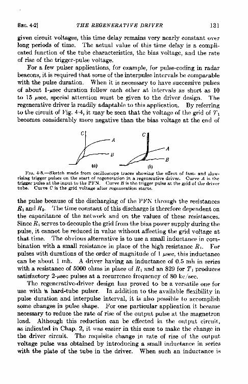
SEC. 4.2] THE REGENERATIVE DRIVER 131
given circuit voltages, this time delay remains very nearly constant overlong periods of time. The actual value of this time delay is a compli-cated function of the tube characteristics, the bias voltage, and the rateof rise of the trigger-pulse voltage.
For a few pulser applications, for example, for pulse-coding in radarbeacons, it is required that some of the interpulse intervals be comparablewith the pulse duration. When it is necessary to have successive pulsesof about l-psec duration follow each other at intervals as short as 10to 15 psec, special attention must be given to the driver design. Theregenerative driver is readily adaptable to this application. By referringto the circuit of Fig. 4“4, it may be seen that the voltage of the grid of Z’1becomes considerably more negative than the bias voltage at the end of
FIG. 4.8.—Sketch made from oscilloscope traces showing the effect of fast- and slow-rishg trigger pulses on the start of regeneration in a regenerative driver. Curve A is thetrigger pulse at the input to the PFN. Curve B is the trigger pulse at the grid of the drivertube. Curve C is the grid voltage after regeneration starts.
the pulse because of the discharging of the PFN through the resistancesRI and RZ. The time constant of this discharge is therefore dependent onthe capacitance of the network and on the values of these resistances.Since R, serves to decouple the grid from the bias power supply during thepulse, it cannot be reduced in value without affecting the grid voltage atthat time. The obvious alternative is to use a small inductance in com-bination with a small resistance in place of the high resistance R,. Forpulses with durations of the order of magnitude of 1 psec, this inductancecan be about 1 mh. A driver having an inductance of 0.5 mh in serieswith a resistance of 5000 ohms in place of R 1 and an 829 for T1 producessatisfactory 2-~sec pulses at a recurrence frequency of 80 kc/see.
The regenerative-driver design has proved to be a versatile one foruse with ‘a hard-tube pulser. In addition to the available flexibility inpulse duration and interpulse interval, it is also possible to accomplishsome changes in pulse shape. For one particular application it becamenecessary to reduce the rate of rise of the output pulse at the magnetronload. Although this reduction can be effected in the output circuit,as indicated in Chap. 2, it was easier in this case to make the change inthe driver circuit. The requisite change in rate of rise of the outputvoltage pulse was obtained by introducing a small inductance in serieswith the plate of the tube in the driver. When such an inductance is

132 DRIVER CIRCUITS [SEC.4.3
used alone, large oscillations are superimposed on the pulse. They maybe damped out, however, by inserting a resistance in parallel with theinductance.
A regenerative driver using a single 829 tetrode provides a power out-put and grid swing that are sufficient to drive the grids of two 715B or5D21 tubes in parallel. This power output is 2 to 3 kw with a grid swingof about 1000 volts. The power output of the pulser is about 250 to300 kw.
4.3. The Multivibrator and Pulse-forming-network Drivers.-Multi-vibrators are used extensively to generate pulses at low-power levels.Several arrangements of the multivibrator circuit are discussed in Vol.19 of the Radiation Laboratory Series. For microwave-radar systems,the so-called “biased multivibrator” has been adapted for use as thepulse generator in the driver of a hard-tube pulser. This circuit is suit-able for driver application because it has a single stable state. It istherefore possible to obtain an output pulse from a biased multivibratoronly when the proper triggering impulse is applied to one of the tubes, andthe length of the interpulse intervals can be determined by a timing cir-cuit that is independent of the pulser.
A driver circuit utilizing a biased-multivibrator as the pulse generatorhas been devised for a 1-Mw hard-tube pulser (described in detail inSec. 5.2). The switch in this pulser consists of three 6C21 triodes inparallel. It is evident from the discussion of switch tubes in Chap. 3that the driver for such a pulser must deliver a pulse power of about15 kw to the three 6C21 grids. The grid-voltage swing required for1-Mw power output from the pulser is about 2.5 to 3 kv. Since it isimpracticable to try to obtain this much power at the output of themultivibrator, it is necessary to use amplification.
The shape and duration of the output pulse from a multivibratordepends on the load and on the values of the circuit elements and tubevoltages. In practice, some variation must usually be expected in theseparameters, and it is therefore necessary to allow sufficient latitude in thecircuit design to accommodate a reasonable range of values. The mostserious aspect of this characteristic of the multivibrator in the driverapplication is the possible variation of pulse duration. In this driverthe difficulty was avoided by introducing an auxiliary means for determin-ing the pulse duration, which consisted of a delay line connected betweenthe output of the driver and the input of the amplifier following themulti vibrat or.
The block diagram of this driver circuit, shown in Fig. 4.9, indicatesthe way in which the pulse duration is determined. The multivibratorpulse generator is constructed so that the pulse fed into the amplifier atB is of longer duration than the pulse desired at the output of the driver.

SEC. 4.3] MULTI VIBRATOR ANDPFN DRIVERS 133
When the leading edge of the pulse reaches A, a voltage wave starts totravel from A to B through the delay line. This voltage wave reaches B
after a time determined by the constants of the delay line. If the pulsefed into the amplifier at B is positive and the pulse voltage at A is nega-tive, it is possible to neutralize the positive voltage at the amplifier input,and thereby to terminate the pulse appearing at A. The pulse durationat the driver output is thus fixed by the time it takes a voltage wave totravel the length of the delay line, independent of the multivibratorcmtput. This arrangement has been expressively called the “tail-biting”circuit.
In order to insure that only one pulse appears at the driver outputfor each trigger pulse, the output pulse of the multivibrator must not
Inputtriggerpulaa Biaaad Buffer output
multivibrator
wFIG.4.9.—Block diagram of the driver for a hard-tube pulser ueing a multivibrator pulse
generator.
last longer than twice the transit time for the delay line. For pulse dura-tions of about a microsecond, this latitude for the multivibrator output isample. When the desired pulse duration is very short, however, morecare must be exercised in the design of the circuit. The buffer amplifieris introduced to minimize the effect of loading on the output pulse shapeand pulse duration obtained from the multivibrat or. If the amplifier iscarefully designed, the shape of the pulse at the driver output can beconsiderably better than that fed into the amplifier, and the dependenceof driver output on multivibrator output is further reduced.
A simplified schematic diagram for this driver circuit is shown inFig. 4“10. The biased multivibrator, which consists of the two halves of a6SN7, delivers a negative pulse to the grid of the normally “on” bufferamplifier tube, a 6L6. A positive pulse is then obtained at the grid ofthe first 3E’Z9 amplifier. The negative pulse that appears at the plate ofthis 3E29 is inverted by means of a pulse transformer, and the resultingpositive pulse is applied to the grids of two 3E29 tubes in parallel. Thenegative pulse obtained at the plates of these tubes is also inverted by apulse transformer in order to give a positive pulse at the grids of the6C21 tubes. A part of the negative pulse at A is impressed across theend of the delay line by means of the voltage dhider consisting of RI
and R,. After traversing the delay line, thk negative pulse appears at B

134 DRIVER CIRCUITS [SEC. 4.3
with amplitude sufficient to neutralize the positive pulse output from the6L6. This negative pulse lasts for a time corresponding to the pulseduration at point A and, if this time plus the delay time is greater thanthe duration of the pulse from the multivibrator, the bias voltage main-tains the 3E29 nonconducting when the pulse is over.
The pulse duration from this driver may be varied by changing thelength of the delay line between points A and B. The switch S,, indi-cated in Fig. 4.10, is provided to facilitate this change. The switch S,
cTo gridof pulsarswitchtube
FIG.
Dela~ line4. 10.—Simplified schematic diagram of the driver for a hard-tube pulser using a
multlvibrator pulse generator and a delay line to determine pulse duration.
is mechanically coupled with sl in order to change the pulse duration atthe multivibrator output at the same time that the length of the delayline is changed. The constants in the multivibrator circuit are chosenso that the pulse delivered to the amplifier is about 25 to 40 per centlonger than the pulse duration desired from the driver.
The operation of this driver requires two of the tubes, the 6L6 andone half of the 6SN7, to be conducting during the interpulse interval.When the pulser is being operated at a low duty ratio, where the inter-pulse interval is about 1000 times as long as the pulse interval, it is desir-able to have the power dissipated by these normally “ on” tubes as smallas possible. The multivibrator power output should be kept small forthis reason also, and the necessary output power from the driver must beprovided by pulse amplification.
Another driver circuit making use of a biased multivibrator has beendevised for the 200-kw hard-tube pulser of a microwave-radar system

SEC.4.3] MULTI VIBRA TOR AND PFN DRIVERS 135
used in aircraft. The switch in this pulser consists of two 5D21 tetrodesin parallel. In this driver, the multivibrator serves a somewhat differentpurpose than it does in the circuit just discussed. The pulse shape andpulse duration are determined in this driver by a current-fed net-work(see Part II for the detailed discussion of pulse-forming networks).The function of the multivibrator is to start and stop the current in thisnetwork. This circuit should, therefore, more properly be referred to as
a ‘‘ PUISe-fOrming-network fiver H rather than a ‘‘ multivibrator driver. ”The operation of this driver circuit is best discussed with reference to
the circuit diagram shown in Fig. 4.11. The two tubes, 6AG7 and 3E29,
%
‘.BCAInput
——
trigger
+
pulse
K1
?.
*
c.
&~—
Y’I-&) ’E”“PI’
Fm.4.11 .—Driver for a hard-tube puhwr using a biased multivibrator with one stable etateand a current-fed network for pulse-shaping.
and associated circuit elements constitute a cathode-coupled biasedmultivibrator. The values of the circuit elements and voltages are suchthat the 6AG7 is normally conducting and the 3E29 is nonconducting.A negative trigger pulse applied to the &d of the 6AG7 makes this tubenonconducting, and the plate rises in potential. As a result, the grid ofthe 3E29 is raised in potential by virtue of the coupling capacitanceC,, and plate current starts to flow. The current flowing in the cathoderesistance of the 3E29 then raises the potential of the cathode of the6AG7 through the niedium of the coupling capacitance C,, keeping thistube in the nonconducting state. The 3E29 remains conducting untilthe potential of the 6AG7 cathode falls sufficiently to allow this tube tobecome conducting again. The time required for the cycle to be com-pleted is determined by the time constant of the capacitance (72and thecathode resistance.
A current-fed network is connected in series with the plate of the3E29. In its simplest form, such a network is a short-circuited line-simulating network, as indicated in Fig. 4.12a. The configuration
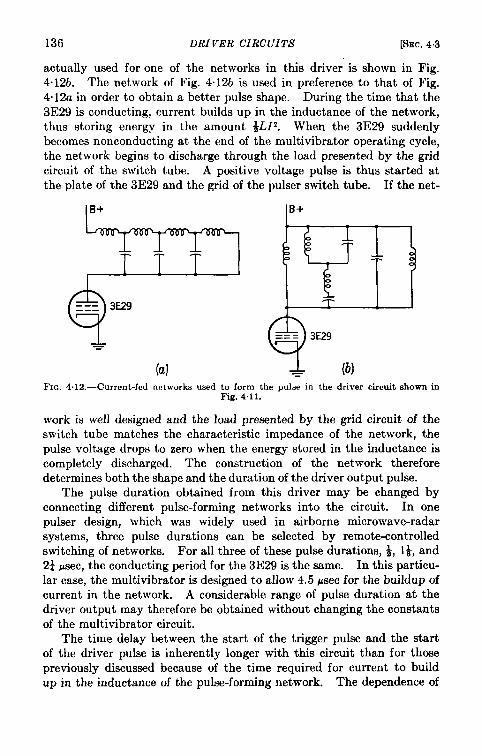
136 DRIVER CIRCUITS [SEC. 43
actually used for one of the networks in this driver is shown in Fig.4.12b. The network of Fig. 4. 12b is used in preference to that of Fig.4.12a in order to obtain a better pulse shape. During the time that the3E29 is conducting, current builds up in the inductance of the network,thus storing energy in the amount 4L12. When the 3E29 suddenlybecomes nonconducting at the end of the multivibrator operating cycle,the network begins to discharge through the load presented by the gridcircuit of the switch tube. A positive voltage pulse is thus started atthe plate of the 3E29 and the grid of the pulser switch tube. If the net-
IB+
FKG,(d & (b)
4.12.—Current-fed networks used to form the pulse in the driver circuit shown inFig. 4.11.
work is well designed and the load presented by the grid circuit of theswitch tube matches the characteristic impedance of the network, thepulse voltage drops to zero when the energy stored in the inductance iscompletely discharged. The construction of the network thereforedetermines both the shape and the duration of the chiver output pulse.
The pulse duration obtained from this driver may be changed byconnecting different pulse-forming networks into the circuit. In onepulser design, which was widely used in airborne microwave-radarsystems, three pulse durations can be selected by remote-controlledswitching of networks. For all three of these pulse durations, ~, l+, and2$ ~sec, the conducting period for the 3E29 is the same. In this particu-lar case, the multivibrator is designed to allow 4.5 psec for the buildup ofcurrent in the network. A considerable range of pulse duration at thedriver output may therefore be obtained without changing the constantsof the multivibrator circuit.
The time delay between the start of the trigger pulse and the startof the driver pulse is inherently longer with this circuit than for thosepreviously discussed because of the time required for current to buildup in the inductance of the pulse-forming network. The dependence of

SEC.43] MULTI VIBRATOR AND PFN DRIVERS 13’?
the pulse duration of the multivibrator output on the circuit voltagesaffects this time delay. If, for any reason, the voltages applied to thetubes of the multivibrator are subject to random variations, the changein time delay appears as time jitter in the output pulse.
Because of the effect just mentioned,. a later version of this driverincorporated a modification of the multivibrator circuit such that the6AG7 tube is returned to the conducting state by the positive pulseobtained by connecting a short-circuited delay line in parallel with thetrigger input as shown in Fig. 4.13. Foc this modification, indicated
I ,+r T
‘B’
PFN
c,
74—-—-:D21
inputtriggerrmlse
p+““”’ Y I YE29i I. . .. .mf~ r
Delay hne
ZA=150 ohms e -
28= 4.5psec
FIG.4.13.—Driver for a hard-tube pulser using a biased multivibrator with one stable stateand one quasi-stable state. The pulse-shaping is obtained with a current-fed network.
in Fig. 4.13, the coupling capacitance between the cathodes of the twotubes is removed, and a direct connection is made in its place. The twotubes have, therefore, a common cathode resistor. The behavior of thiscircuit when a negative trigger pulse is applied to the grid of the 6AG7 isthe same as that for the circuit of Fig. 4.11. The 3E29 is changed fromthe conducting to the nonconducting state by the positive pulse at the6AG7 grid, and, because it is again desired to have 3E29 conducting for4.5 psec, the delay line is constructed so that it has a two-way transittime of 4.5 psec. This circuit, as well as the earlier version, has a singlestable state, but, because of the long time constants in the grid circuits,the state in which the 3E29 is conducting can be considered quasi-stableas far as the circuit operation is concerned. The principal advantages ofthis arrangement over the previous one are a smaller dependence ofcircuit behavior on the 3E29 characteristics, and the possibilityy of bettercontrol over the length of the PFN-charging period.

138 DRIVER CIRCUITS [SEC. d-~
For reasons already mentioned, it is desirable to have the normally“on” tube of the multivibrator dissipate as little power as possible. Itis also desirable to keep the conducting period for the 3E29 short in orderto maintain a high over-all efficiency.
A pulse-forming-network driver can also be designed with a voltage-fed network. In this case the driver is a line-type pulser of the typedescribed in detail in Part II of this volume. Although the pulse genera-tor used in the bootstrap driver, discussed in Sec. 4“1, is such a line-typepulser, the output power is too small for the driver function, and it isnecessary to provide amplification. The subsequent development ofpulse-forming networks and satisfactory gaseous-discharge tubes capableof handling high pulse power has eliminated the necessity of amplification.With the 3C45, 4C35, and 5C22 hydrogen thyratrons it is now possibleto design line-type pulsers having a range of pulse-power output from afew kilowatts to several megawatts.
The schematic circuit for one possible arrangement of a pulse-forming-network driver using a voltage-fed network is shown in Fig. 4“14. The
Chatia$g —-J
Powersupply
puke
&
Fm. 4.14.—PuL?-e-forming-network driver for a hard-tube ptdser.
PFN is charged during the interpulse interval from the d-c power supplythrough an inductance and a diode in series. The output pulse isinitiated by the application of a positive trigger pulse to the grid of thegaseous-discharge switch tube. When the tube is conducting, the PFNdischarges into the load, which consists of the cathode resistor and thegrid circuit of the high-vacuum switch tube of the pulser output circuit.The pulse shape and the pulse duration are determined by the character-istics of the PFN and its discharging circuit. The reader is referred toPart II for further details concerning the operation of line-type pulsers.
When the pulser application requires only one pulse duration andrecurrence frequency, it is unnecessary to have a diode in the chargingCircuit of the network. With the diode, however, it is possible to changerecurrence frequency over a considerable range, and the pulse durationmay be changed by connecting different networks into the circuit.

SEC. 4.3] MULTI VIBRA TOR AND PFN DRIVERS 139
By using a pulse transformer, it is possible to connect the cathode ofthe gaseous-discharge tube to ground, as shown in Fig. 4.15, and thus toeliminate the need for a filament transformer with high-voltage insulation.
PFN
supply—
Inputswitchtube
.FIG.4.15.—Pulse-forming-networkdriverwith pulse.trrmsforrnercouplingto the grid of
thehigh-vacuumswitchtub.
A possible disadvantage is that the introduction of the pulse transformermay result in a somewhat poorer pulse shape at the grid of the high-vacuum switch tube.

CHAPTER 5
PARTICULAR APPLICATIONS
BY G. h’. GLASOE
5.1. The Model 3 Pulser—A Light-weight, Medium-power Pulserfor Airborne Radar Systems.—The original specifications for this pulser,based on the requirements for a light-weight airborne search radar, ASV,and an aircraft-interception radar, AI, were formulated in the winter of1941. By the summer of 1945 this pulser had been incorporated intosix different radar systems and their various modifications. The pulserwas manufactured in very large numbers by the Stromberg-CarlsonCompany and the Philco Corporation. A revised model of the pulser,Mark II, in which improvements were made in engineering and manu-facturing details, was manufactured during the last year of the war. Afew circuit modifications were also incorporated as a result of the experi-ence gained in the operation of the original version, Mark I. The revisedpulser was designed to meet the requirement that it be physically andelectrically interchangeable with the original unit. The stringent require-ments placed on the size and weight of this pulser resulted in some depar-tures from accepted engineering practices. Improvements in techniquesand in the design and manufacture of components, however, warrantedsuch departures, and extensive laboratory tests proved their feasibility.Because of the small size of this pulser compared with others that hadpreviously been constructed for an equivalent power output, the unit wasfacetiously referred to as the “vest-pocket pulser.”
The Model 3 pulser was designed to meet the following specifications:Output pulse power: 144 kw (12 kv at 12 amp).Duty ratio: 0.001 maximum.Pulse duration: 0.5, 1.0 and 2.0 psec. (Remote control of pulse
selection. )Size: must fit into a cubical space 16 in. on a side.Weight: preferably no greater than 60 lbs.Ambient-temperature range: – 40 to +50”C. (External fan to be
provided with ambient temperature above +30°C.)Altitude: must operate satisfactorily at 30,000 ft.Input voltages: 115 volts at 400 to 2000 cycles/see and 24v d-c.
(The a-c frequency range was changed to 800 to 1600 cycles/seewhen the revised pulser was being designed.)
140

SEC. 5.1] LIGHT- WEIGHT, MEDIUM-POWER P 1’LSER 141
The design of a pulser to meet these specifications was undertakenbefore satisfactory pulse transformers and line-type pulsers were devel-oped. The design, of necessity, included the high-voltage power supplyassociated with a hard-tube-pulser design. The coml)ined size, weight,and altitude specifications therefore required that the pulser be housedin an airtight container in order to maintain atmospheric pressure aroundthe high-voltage parts of the circuit, regardless of the reduced externalpressure at high altitude. The need for an airtight housing complicatedthe problem of heat dissipation. Because the lack of ventilation and thehigh external temperature caused the components to operate at hightcrnpcraturcs, it was imperative that the over-all efficiency be as high aspossible. The size and weight specifications imposed the necessity ofusing small components, resulting in small factors of safety. The com-pleted pulscr Imit was mounted on a square base 15 in. by 15 in. by 44 in.The airtight housing was a cylinder having a diameter of 15 in. and a{lomc-shaped end of dimensions such that the over-all height was 11$ in.The combined heights of the base and housing were 16 in. A spaceunder the base was provided for mounting a magnetron, TR tube, pre-amplifier, and miscellaneous parts associated with the r-f components.The original unit manufactured by Stromberg-Carlson weighed 64 lb,and the l’hilco unit weighed 60 lb. The revised pulser, which wasmanufactured by Stromberg-Carlson, weighed 53 lb. Photographsof the Stromberg-Carlson pulser are reproduced in Figs. 5.1 and52, and the schematic diagrams for these two units are shown inFigs. 5.4 and 5.5.
The control circuit and connections to the primary power source areomitted for the sake of clarity.
The Output Circuit.—The original plans for the Model 3 pulser calledfor its operation with the 2.J21 and 2,J22 magnetrons. THe 725A magne-tron, \vhich was developed later, replaced the 2J21 as soon as it becameavailable. From a knowledge of the operating characteristics of thesemagnetron oscillators, it was decided that the output voltage pulseobtained from the pulser could be allowed to drop as much as 2 per centduring a l-psec pulse without seriously affecting the frequency of themagnetron output. The minimum capacitance of the storage condenserto be used in the pulser was, therefore, determined from the relationAVz = 11At/C., as indicated in Chap. 2. For a pulse voltage of 12 kvand a pulse current of 12 amp, the capacitance of the storage condenser is
c. =12 x 1 x 10–6
‘2 X 1o-’ x 12 x 100 = 0.05 X 10⁻⁶ farad.
Operation at a pulse duration of 2-~sec was considered satisfactory, event bough it resulted in a 4 per cent drop in pulse voltage at the magnetron

142P
AR
TIC
UL
AR
AP
PL
ICA
TIO
NS
[SE
C.5.1
—,.
.....
.-—

SE
C.
143
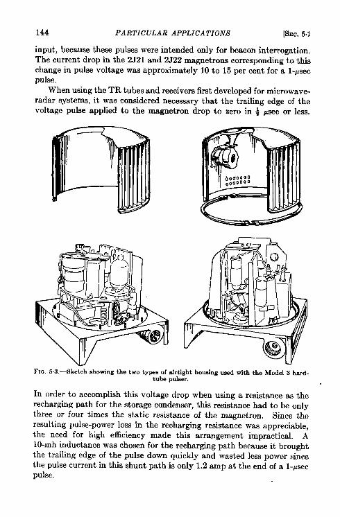
144 PARTICULAR APPLICATIONS [SEC.5.1
input, because these pulses were intended only for beacon interrogation.The current drop in the 2J21 and 2J22 magnetrons corresponding to thischange in pulse voltage was approximately 10 to 15 per cent for a l-psecpulse.
When using the TR tubes and receivers first developed for rnicrowave-radar systems, it was considered necessary that the trailing edge of thevoltage pulse applied to the magnetron drop to zero in ~ psec or less.
——
FIG.5.3.—Sketch showing the two types of airtight housingusedwiththe Model3 hard.tube pufser.
In order to accomplish this voltage drop when using a resistance as therecharging path for the storage condenser, this resistance had to be onlythree or four times the static resistance of the magnetron. Since theresulting pulse-power loss in the recharging resistance was appreciable,the need for high efficiency made this arrangement impractical. A
lo-mh inductance was chosen for the recharging path because it brought
the trailing edge of the pulse down quickly and wasted less power since
the pulse current in this shunt path is only 1.2 amp at the end of a l-~sec
pulse.

SEC.5.1] LIGHT- WEIGHT, MEDIUM-POWER PULSER 145
In the original design the isolating element in series with the high-voltage power supply was a 5-mh inductance. Oscillations in the voltageof the storage condenser occurred during the charging interval, as indi-cated in the curves of Figs. 2“39 and 2.40. The amplitude of these oscil-lations was sufficient to induce voltages in other parts of the circuit,
-Low-capacitancewinding
‘“” ‘ mi=mcReT:::L
@
0.25 Power-SUPPIY0.15 0.15 =) current
20072
723:;4
3&4
mFm. 5.4.—Schematicdiagramof theoriginalModel3 hard-tubepuleer.
Pulse-selecting
“’?*F:5k:1
13c+
7!J
&
-Ilo,bl,,, ,3, ,.ol<,;;\mJto
-f8WWto
0.3 0.3 ,2 +1300 ,272 —
3;4 3:24 3;4_
m
!: r-=J=-~~~~~$~e0.3 ---- -Y-
r
!SiJ
Magnetron3B2 filament
2mh-Low-capacitance
. winding
Fm. 6$.-Scheme.tic dlagrarn of the revised Model 3 hard-tube pulser,
causing false signals to appear on the indicator of the radar system. Itwas therefore necessary to introduce a 500-ohm resistor in series with the5-mh charging inductance in order to eliminate these oscillations. Theresult of the addition is shown in Fig. 2.40. Since it proved difficult tofind a satisfactory 500-ohm resistor that was not too bulky, the 5-mhinductance was soon replaced by a 10,000-ohm resistor. The shape ofthe trailing edges obtained with the lo-mh recharging path and the

146 PARTICULAR APPLICATIONS [sm. 5.1
10,000-ohm isolating resistor for the three pulse durations is shown inthe oscilloscope traces reproduced in Fig. 2“25. The traces reproducedin Fig. 2“19 indicate the corresponding behavior when the 10-mh induct-ance was replaced by a 10,000-ohm resistor.
As the development of radar systems and components progressed, itbecame evident that the importance of having a steep trailing edge onthe voltage pulse had been overemphasized. Therefore, in the design ofthe revised version of the pulser less attention was given to this detail.Perfectly satisfactory operation of the radar system could be obtainedwith a voltage pulse that dropped to zero in as much as 1.5 ysec.
The use of an inductance m the recharging path causes a positivebackswing voltage to appear at the end of the pulse. This positive volt-age is added to the power-supply voltage at the plate of the switch tubeand may result in sparking, particularly when the power-supply voltageis near the safe upper limit for the tube. It is therefore necessary tointroduce a shunt diode, as indicated in Chap. 2. When an inductiveresistor is used as the recharging path, and the magnetron is connecteddirectly to the output of the pulser, the shunt diode is unnecessary.(This was one of the modifications incorporated into the revised design asa result of the relaxed requirement on the time for the voltage to fall tozero.) The photographs of Fig. 2.27 show the voltage pulses obtainedwith an inductive resistor in parallel with the magnetron load.
It is generally desirable to have some available means of monitoringthe current through the magnetron. In a hard-tube pulser, the averagemagnetron current is equal to the average current corresponding to therecharging of the storage condenser. This current may be measuredsimply by connecting an ammeter in series with the recharging path asindicated in the Figs. 5.4 and 5.5. This meter must be bypassed by acapacitance sufficiently large to prevent the meter from being damagedby the pulse current that flows while the switch tube is conducting. Theprecautions necessary for such average-current measurements are dis-cussed in detail in Appendix A. A resistor is usually connected in parallelwith the meter in order to provide a conducting path when the meter isdisconnected. This resistance must be large enough so that it introducesa negligible error in the ammeter reading, but not so large that it appreci-ably increases the condenser-charging time constant. (In the Model 3pulser this resistance was about 200 ohms.) When a shunt diode isused in the pulser, the average-current meter must be connected in sucha way that it measures the sum of the currents in the diode and therecharging path.
When the design of the Model 3 pulser was begun, no really satis-factory switch tube was available. The 304TH, which had been used inprevious designs, required so much cathode-heating power that it could
SEC.5.1] LIGHT- WEIGHT, MEDIUM-POWER PULSER 147
not be considered for a small airtight unit. The development of the715B provided a tube that was capable of withstanding the high voltageand had sufficient cathode emission for the required plate current.Since this tube has an oxide cathode, much skepticism was expressedconcerning its suitability for an application where a plate voltage of asmuch as 15 kv and a pulse-plate current of almost 15 amp were needed.Extensive life tests, however, showed that factory tests could be devisedthat would eliminate the relatively few tubes that could not meet thepulser requirements.
The 715B tube is a tetrode and, as indicated in Chap. 3, its pulsecharacteristics make it very suitable as a pulser switch tube. The biasvoltage that is necessary to keep the tube nonconducting during theinterpulse interval is about —500 volts, although occasional tubes requireas much as —750 volts. The Model 3 pulser was designed with a biasvoltage of at least —650 volts in order to insure a negligible plate currentduring the interpulse interval for the majority of 715B tubes. The biasvoltage and the screen-grid voltage of +1250 volts are both obtainedfrom the power supply in the driver circuit. Since a high resistance isconnected in series with the screen grid as a protection against excessivescreen grid current, it is necessary to bypass the screen grid to the cathodewith a reasonably large capacitance. This capacitance was 0.06 pf inthe original model, but was increased to 0.3 ~f in the revised pulser.The increase in size of the bypass capacitance improved the pulse shapefor marginal tubes, since it decreased the drop in screen voltage duringthe pulse.
With a screen-grid voltage of 1250 volts and a positive grid drive of200 to 250 volts, a pulse current of 12 amp can be obtained in the magne-tron for a tube drop of about 1.5 kv in the 715B. The plate current atthe start of the pulse consists of the load current and the current thl oughthe 10,000-ohm isolating resistor. At the end of the pulse, the currentthat has been built up in the 10-mh shunt inductance is an additionalcontribution to the plate current. As stated previously, this additionalplate current is about 1.2 amp for a l-psec pulse. Thus, the plate cur-rent should increase from 12 amp to 13.2 amp during the pulse if themagnetron current remains constant. The drop in the voltage on thestorage condenser, however, causes the load current to decrease by anamount which may actually be more than the increase in current occurringin the 10-mh inductance, and as a result the net plate current may be lessat the end than at the beginning of the pulse.
A plot of the components of the cathode current in a 715B switchtube used in one of these pulsers is shown in Fig. 5.6. The pulse currentin the magnetron load, the current in the 10-mh inductance, the screen-grid current, and the total cathode current were measured by means of a

148 PARTICULAR APPLICATIONS [SEC. 5.1
synchroscope and calibrated noninductive resistors. The block labeled“l., + ZIO~Am, + errors” was not measured, but its magnitude agreeswell with the expected value. With a power-supply voltage of 12 kvand a magnetron-pulse voltage of 10.5 kv, the current in the isolatingresistor is about 1 amp, which leaves a value of about 0.5 to 0.9 amp forthe control-grid current. This value agrees with the pulse characteristicsfor the 715B shown in Fig. 3.7. The drop in voltage on the 0.05-pf
‘m1s[16;1
+lZkv
16
14
* 12
ig lo 2.3a
Eg
8 is cath&Jek* currant3 pul*~ 6~
9.3a4
2
001 2
Timeinfi sec
atrs 1.9a
mh/ 2.2a
‘fl Envelope
FIG. 5.6.—Components of 715B cathode+current pulse with magnetron load.
storage condenser for a 2-psec pulseshould be about 480 volts. Theobserved drop in magnetron cur-rent was 3 amp, corresponding toa dynamic resistance of 160 ohms,a value that is also in agreementwith the known characteristics ofthe 725A magnetron used for thesemeasurements. From this plot itmay be seen that the total cathodecurrent actually decreases slightlyduring the pulse. The slight de-crease in the screen-grid currentis due to a drop in screen-grid volt-age during the pulse caused by abypass condenser of insufficientcapacitance (0.06 pf).
Because of the high frequencyof the primary power source, 400 to2400 cycles/see for the airborneradar systems, it was possible toconsider using a voltage-doublerrectifier for the high-voltage sup-ply. The size of the power trans-former and the voltage on the filter
condensers for this design were less than those for an equivalent half-waveor full-wave rectifier. The over-all specifications for the systems using the
“Model 3 pulser called for reasonably good regulation of thevoltagefrom thealternators. Therefore, because the inherent voltage regulation of thevoltage-doubler power supply was poor, it was necessary to specify thatthe same duty ratio be used for each of the three pulse durations. Thehigh-voltage power supply in this pulser consisted of two O.15-pf 8-kvcondensers in a single can, and two RKR72 rectifier tubes. (Later the3B24 became available and replaced the RKR72.) The high voltagecould be changed by means of an 8-ohm variable resistor connected inseries with the primary of the high-voltage transformer. In order to

SEC. 5.1] LIGHT-WEIGHT, MEDIUM-POWER P ULSER 149
cover a wider range of voltage without using a larger resistance, there werethree taps on the transformer primary. The regulation of the powersupply was considerably poorer with the resistance in the circuit. Thecurves of Fig. 5.7 indicate the regu-lation obtained with and withoutthe 8-ohm resistance.
The average current taken fromthe high-voltage power supply dur-ing the operation of a pulser servesas a convenient means of monitor-ing the circuit behavior. A power-supply current that is higher thanthe value corresponding to the av-erage current in the magnetron in-dicates the breakdown of insulationsomewhere in the high-voltage partof the circuit. In this way, it isoften possible to detect the start ofbreakdown of the insulation in thefilter and storage condensers. The
5Power supply voltage in kv
FIG. 5.7.—Regulation obtained withthe voltage-doubler power supply used in alight-weight medium-power airborne pulser.Curve A is for S ohms in series and B is forno resistance in series with the primary ofthe power transformer.
average current is measured in the ground connection to the power supplyin the same manner used to measure the magnetron average current. Inthis pulser, the average power-supply current was about 5 ma higher thanthe average magnetron current, in the range 8 ma to 12 ma, when a 0.001duty ratio was used.
One of the major circuit modifications made in the design of therevised Model 3 pulser was a change in the high-voltage power supply.At the beginning of the description of the pulser output circuit, it isstated that a 2 per cent drop in pulse voltage was considered allowablefor a l-~sec pulse. One of the factors involved in this consideration wasthe physical size of the storage condenser. If it had been possible to usea capacitance larger than 0.05 ~f in the available space, a drop in voltagesmaller than 2 per cent would have been desirable. A smaller drop involtage during the pulse was obtained by combining the condensers of thevoltagedoubler rectifier with the storage condenser, as shown in Fig. 5.5.The same condensers serve both purposes, and the effective storagecapacitance was therefore 0.15 pf. Thus, the drop in voltage is one thirdof that obtained with the 0.05-pf condenser of the original design.
The power-supply arrangement of the revised pulser had one dis-advantage, namely, that the effective filtering action was not as goodas that obtained with the original arrangement. This disadvantage wasalleviated, however, by the fact that the minimum frequency of the pri-mary power supply had been raised from 400 cps to 800 cps by the time

150 PARTICULAR APPLICATIONS [SEC. 5.1
this revision was considered. With the 800 cps a-c supply, a smallamount (two or three per cent) of amplitude jitter was observable on themagnetron current pulse. This small amplitude jitter was not found tohave any observable effect on the magnetron operation.
The Driver Circuit.—The regenerative driver designed for this pulserused an 829 tube and a GE 68G627 pulse transformer. The circuit forthis driver is discussed in Sec. 4.2 and is shown in detail in Figs. 5.4 and5.5. The power supply for the driver consisted of two half-wave recti-fiers, one for the positive and one for the negative voltages required. Thesame positive voltage was used for the 829 plate and the 715B screen grid.The 829 screen grid and bias voltages were obtained from taps on thebleeder resistance connected across the two parts of the power supply.In the revised design, the filter condensers in the driver power supplywere made considerably smaller than those in the original, again becauseof the higher frequency of the a-c input.
The pulse-forming networks used in the early driver units consistedof several inductance and capacitance sections. As stated in Sec. 4.2,the impedance of these networks is not critical, so it was possible to usestandard sizes of condensers and then adjust the inductances to producethe desired pulse duration. The general procedure in designing such anetwork is to make an approximate calculation of the values of LN andC’. from the two relationships r = 2- and ZN = d~i withz. = 1000 ohms. The actual value of L. is then determined empiricallyusing the nearest standard condenser size. Once the constants for thenetworks are found, it is somewhat of a problem to control the productionmethods so as to have pulse durations that lie within a + 10 per centtolerance about the nominal value. This problem arises from the factthat the actual pulse duration depends on many factors, such as thenetwork itself, the pulse transformer, the stray inductances and capaci-tances in the driver circuit, the tube characteristics (to some extent),and also the load presented to the driver by the grid circuit of the switchtube. The final procedure adopted by the pulser manufacturers was totest each completed network for proper pulse duration, rather than todepend on inductance and capacitance measurements.
Experience with the regenerativedriver circuit indicated that asatisfactory pulse shape could be obtained with pulse-forming networksthat were reduced to single inductances and condensers, at least for apulse-duration of 1 ~sec or less. Accordingly, the networks used in therevised design were built in this manner, as shown in Fig. 5.5. It thust,ecame feasible to make the single inductance variable, and thereby tohave an available means for varying the pulse duration. In the unitsman ufact ured by the Stromberg-Carlson Company the inductance wasvaried by means of a copper slug that could be moved toward or away

SEC. 5.1] LIGHT- WEIGHT, MEDIUM-POWER PULSER 151
from the end of the coil. This copper slug provided an adjustment ofabout f 10 per cent in the pulse duration. In units manufactured bythe PhIlco Corporation, the variation was obtained by means of a ferro-magnetic slug that could be moved along the axis of the coil. A variationof about +20 per cent was made available by this arrangement. Thevariable inductance proved to be a great convenience because it allowedthe pulse duration to be adjusted after the completion of the whole driverunit.
Protective Measures. —Because of the strict limitation on the size ofthe Model 3 pulser, it was decided that a minimum of time-delay andoverload-protection devices would be incorporated. Consequently, thecontrol circuit was made as simple as possible. Two relays were pro-vided to be actuated by the available 24 v d-c. The first controlled thea-c input to all except the high-voltage transformer. By energizing thesecond relay, the high-voltage power supply was turned on. The onlycontrol over the delay time required after turning on the filaments andbefore turning on the high voltage was a sign warning the operator towait three minutes. Instead of a relay for overload protection, two fuseswere provided, a 10-amp fuse in the main a-c line to the pulser, and a5-amp fuse in series with the high-voltage power transformer.
In the original unit, a bleeder resistance was provided across thehigh-voltage power supply. When the input circuit to the power trans-former was opened, this bleeder reduced the voltage on the filter condenserrapidly enough to give reasonable protection against electric shock.The bleeder resistance could not be used with the revised pulser, however,and it was therefore necessary to provide a shorting device. This devicewas a mechanically operated shorting bar that short-circuited the powersupply when the airtight housing was removed.
Heat Dissipation. -Since the unit was required to be airtight, it wasnecessary to circulate the air within the housing in order to obtain asmuch heat transfer as possible to the walls. This circulation was accom-plished by means of a small blower with a 24-v d-c motor. The outside ofthe housing was corrugated to increase the surface area exposed to theexternal air. The power input to the original pulser was about 45o wattsfor an output of 144 watts. Thus, about 300 watts were dissipated withinthe airtight container. The temperature rise within the unit under theseconditions was about 55”C. With an external fan blowing air againstthe outside of the housing at the rate of 60 fts/min, this temperature risewas reduced to about 40”C. The heat dissipation in the revised pulserwas reduced slightly from the above figure and, with improved heattransfer to the walls of the housing, the internal temperature rise wasabout 40°C without an external fan. In the revised design, better heattransfer to the outside air was obtained by the use of a double-walled

152 PARTICULAR APPLICATIONS [SEC. 5.2
housing. The internal blower forced the heated air to pass between thewalls of the inner and outer housing wall, as shown in the sketch in Fig.5.3. Because of the high temperature at which the components of thispulser must operate, special attention was given to the choice of thecondensers. The Sprague Vitamin Q condensers proved satisfactory upto 105°C, and were therefore used in both the original and revisedModel 3 pulsers.
6.2. The Model 9 Pulser—A 1-Mw *d-tube Pulser.-The needfor a high-power pulser to be used in the testing of magnetrons becameurgent early in 1941. The research and development that was startedat this time led to the design of a hard-tube pulser that could deliver apulse power of 1 Mw (25 kv at 40 amp) to a magnetron. The originaldesign of this unit was called the Model 4 pulser, but after some modifica-tions were introduced, particularly in the driver circuit, the pulser becameknown as the Model 9. In addition to its use in determining the per-formance characteristics of magnetrons, this pulser was used in someground-based radar systems. One of these systems in particular waswidely used as a mobile radar unit in both defensive and offensive opera-tions during the war. The Model 9 pulser was used in this radar applica-tion because its operational characteristics satisfied the requirements forprecision ranging and automatic following. The operational use of thisradar system demanded that a very high degree of reliabilityy be main- ‘1tained over long periods of time under conditions of almost continuousoperation. Because of the somewhat unsatisfactory life of the availableswitch tubes and magnetrons with the full 1-Mw pulse power, the pulserwas operated at a pulse-power output of about 800 kw.
The Model 9 pulser was designed to meet the following specifications:Output pulse power: 1000 kw (25 kv at 40 amp).Maximum duty ratio: 0.002.Pulse duration: 0.25 to 2.0 psec (remote control of pulse selection).Size and weight: As small as possible compatible with good engineering
design.Input voltage: 115 volts, 60 cycles/see, single phase (the units for the
mobile radar system were built for three-phase supply).
The specified voltage and current output for this hard-tube pulserrequired that the high-voltage power supply be designed for about 30kv and 100 ma. Because of this high voltage and average current, itwas impractical to design the pulser and the power supply as a singleunit. Consequently, the pulser was built in one cabinet and the powersupply in another, necessarily making the total weight larger than itwould be for a single unit. The completed pulser occupies a cabinet26 by 34 by 55 in. and weighs about 800 lb. The power-supply cabinet is

SEC.5.2] A 1-MW HARD-TUBE PULSER 153
approximately the same size but weighs about 1200 lb. The photographsreproduced in Fig. 5.8 indicate the disposition of the components in thepulser cabinet. The schematic diagram for the hlodel 9 pulser withcontrol circuits omitted is shown in Fig. 5.9.
The Output Circuit.—For the measurements necessary in determiningthe performance characteristics of a magnetron, it is desirable to have theshape of the output pulse from the pulser as rectangular as possible.It was therefore decided that the top of the voltage pulse should be flat tobetter than the 2 per cent figure allowed in the Model 3 pulser design.The choice of the actual energy-storage capacitance to be used wasinfluenced by the available high-voltage condensers. Since a value of0.125 pf was chosen, the drop in pulse voltage for a l-psec pulse is about1.3 per cent at the full output power from the pulser (25 kv at 40 amp).This value of the storage capacitance was considered sufficient for themajority of the applications, and for many of these, the drop in voltagewas not greater than 1 per cent because the actual pulse current usedwas less than the maximum value of 40 amp.
As in the case of the Model 3 pulser, the trailing edge of the voltagepulse was required to drop to zero in less than 0.5 psec. With a magne-tron load, the rate of fall of the pulse voltage depends on the amount, ofenergy stored in stray capacitance during the pulse, and on the nature ofthe recharging path for the storage condenser. The stray capacitanceand voltage were larger for the Model 9 pulser than for lower-powerpulsers, and consequently, if a resistance were to be used as the recharg-ing path, its value would have to be so small that a large amount of pulsepower would be wasted. It was therefore decided to use a 5-mh induct-ance in place of the resistance, this value being adequate even for the0.5- and 0.25-psec pulses.
The isolating element in series with the high-voltage power supply isa 10,000-ohm resistance. Thus, a pulse current of about 2.5 amp flowsthrough this resistance at maximum pulse voltage output from the pulser.The power lost during the pulse interval in this resistance at the maximumduty ratio of 0.002 is, therefore,
P = l~R.,(PRF) = (2.5)’ X 104 X 0.002 = 125 watts.
If the maximum duty ratio of 0.002 corresponds to operation at a pulseduration of 1 psec and a PRF of 2000 pps, the interpulse interval is5 X 10–4 sec. If it is assumed that the 10,000-ohm resistor constitutesthe entire recharging path for the storage condenser, the power dissipatedduring the interpulse interval may be calculated as outlined in Sec. 2.4.Thus, in this case, the time constant is
RC = 104 X 0.125 X 10-0 = 1.25 X 10⁻³ sec.

154 PARTICULAR APPLICATIONS [SEC.5.2
and the interpulse interval is equal to 0.4RC. The rms charging cur-rent is then 1.006 times the average current. For operation at fullpulse power and 0.002 duty ratio, the average recharging current is80 ma, so (1,)- = 80.5 ma, and the power lost in the charging resistor is(0.08)’ X 104 = 64 watts. The isolating resistance must therefore becapable of dissipating about 200 watts. Because of the high voltage
FIG. 5.8.—Photographs of
across this resistance, the pulser was designed with four 2500-ohm unitsin series.
In order to eliminate the backswing voltage inherent in the use ofthe inductance recharging path, it was necessary to incorporate a shuntdiode into the pulser design. This diode had to be capable of passing apulse current of several amperes, and of withstanding an inverse voltageof 25 kv. The choice of tube for this function was somewhat limited, andit proved to be more economical of space and cathode power to use two8020 diodes in parallel, rather than a single large tube. It was necessary

SEC.52] A 1-MW HARD-TUBE PULSER 155
to use more than one 8020 tube because the plate dissipation was greaterthan that allowed for a single tube.
The average magnetron current is measured by a meter connected inseries with the recharging path for the storage condenser. In the Model9 pulser, a current-sensitive relay is connected in series with this meter.The contacts of this relay are connected in series with the primary winding
the Mo del 9 1-Mw pulser.
of the transformer used to heat the magnetron cathode. By adjusting aresistance in parallel with the coil of this relay, it is possible to have themagnet ron-cat bode heater current shut off when the average magnetroncurrent reaches a certain minimum value. This feature was added to thispulser because the back-bombardment heating of the magnetron cathodebecame large enough at high average power to keep the cathode hotwithout any current in the heater. This automatic reduction of thecathode-heating power minimized the danger of overheating the cathode,and the consequent shortening of the life of the magnetron.

4700 2—----- ------ --.---—. ‘4.6 k+_. -_-_ -___ -__ --—-- ------ --- —-—---- ----------- ------- -----. ,
10k /{ h“ +450
]8k I 1 n i f4 I- +750v I.
i.- ;
iI!II1IIII
:1$
. , 1 1 1 1 c1.0+ t
8k
4.0 ~
E
5U4
m110v60Cps
-- -——
12h4.05
4.9I
y
0.25
“LwdLu!d~~i I
@ -kiiiiii--—---——-—-- rControlcircuitsaranotshown ‘- ~
—
FIG. 5.9.—Schematic diagram for the Model 9 1.Mw hard-tube pulser. Control circuits are not shown, N

t?iEG.5.2] A 1-MW H.lRD-TUBE PULISER 157
A survey of available tubes that could be used as the switch in theModel 9 pulser indicated that the Eimac 1000 UHF triode, later calledthe 6C21, was the best choice. The pulse characteristics for this tube,shown in Fig. 3“10, indicate that three tubes in parallel are required toobtain a pulse current of 40 amp in the pulser load. It proved to bemore economical of cathode-heating polver and grid-drive power to useseveral of these tubes in parallel, instead of a single large tube that couldwithstand the plate voltage of 30 kv and carry the required pulse current.Although the 1000 UHF was rated for a considerably lower plate voltage,laboratory tests proved that the tube could be operated at 30 kv underthe conditions of pulse operation.
The pulse currents in the 10,000-ohm isolating resistance and in the5-nlh recharging inductance must be added to the load pulse currentwhen determining the total plate current for the switch tubes. For a40-amp load current in the Model 9 pulser, the total plate current is45 to 50 amp. The curves of Fig. 3.10 i~dicate that this plate current canbe obtained with three 6C21 tubes in parallel if the positive grid drive is1000 to 1500 volts and the tube drop is 4 to 5 kv. Under these conditionsthe pulse-grid current becomes about 1.5 to 2.5 amp for each tube. Inorder to keep the 6C21 tube from conducting during the interpulse inter-val, the grid must be biased at least 1200 volts negative when the platevoltage is 30 kv. The pulser was designed with a grid bias of 1500volts to insure a negligible plate current during the interpulse interval forany tube. The grid-driving power necessary for the switch-tube opera-tion in this pulser is therefore about 20 kw. Thk value is not unreason-ably large for a 1-Mw pulser.
The Driver Circuit .—The driver circuit used for the Model 9 pulserhas been described in Sec. 43. A block diagram and a simplified sche-matic of this driver are shown in Figs. 4“9 and 4“10. The 3E29 tube waschosen for the final pulse amplifier in this driver because the grid swingof 2.5 to 3 kv required for the 6C21 tubes could not be obtained from an829 tube. As stated in Chap. 3, the 829 tube has a plate-voltage ratingfor pulse operation of 2 kv, whereas the 3E29 was designed for a platevoltage of 5 kv. Although the grid current of 5 to 8 amp in the three6C21 tubes could be obtained with a single 3E29 tube, the driver wasdesigned with two of these tubes in parallel in order to provide a greaterfactor of safety. A plate voltage of 4 kv and a screen-grid voltage of720 volts was used for these final amplifier tubes in the driver.
Since the voltage output available from the 6L6 buffer amplifierfollowing the multivibrator was not sufficient, an intermediate amplifiertube was necessary. An 829 could serve this purpose, but in order toreduce the number of tube types, another 3E29 was used instead, whichoperated with the plate voltage and the screen-grid voltage obtainedfrom a 750-volt polver supply.

158 PARTICULAR APPLICATIONS [SEC.5.2
As stated in Sec. 4.3, the pulse duration obtained from this driver ischanged by varying the length of the delay line in the feedback (tail-biting) circuit. This variation is accomplished by means of a series oftaps onthedelay line which can deselected by a switch. This switchismechanically linked with another switch that changes the constants inthe multivibrator in order to keep the pulse duration for the multivibratorabout 25 to 40 per cent larger than that desired at the output of the driver.
The driver for the Model 9 pulser was constructed in a unit physicallyseparable from the rest of the pulser. This arrangement provides aneasy means of servicing the driver and making any desired modifications.All the d-c voltages necessary for the driver circuit, with the exception ofthe 4-kv supply for the 3E29 plates, are obtained from power suppliescontained in the driver unit.
Modifications to Obtain Continuously Variable Pulse Duration over the
Range 0.5 psec to 5 psec.—A slight modification of the driver circuit madeit possible to vary the pulse duration continuously over the range 0.5to 5 psec. This variation was accomplished by removing the delay lineentirely and introducing a variable resistance in place of the switch andthe series of fixed resistances in the grid circuit of the normally “on”half of the 6SN7 multivibrator tube. Since the pulse duration is approxi-mately an exponential function of this grid resistance, a tapered potentio-meter was designed to allow the pulse duration to vary with the position
of the adjustment control in a rea-I.P
To sonably linear manner. The mod-~r~ ified multivibrator is shown in Fig.
5.10. The circuit elements indi-cated in heavy lines are those thatwere changed from the originalarrangement shown in Fig. 5.9 inorder to obtain satisfactory opera-tion over the 0.5-to 5.o-psec range
-15v +200V in pulse duration. The only otherFIC.5.10.—Modifiedmultivibratorcircuit
for driverin Model 9 pulser to provide pulse change in the driver circuit nec-durations continuously variable over the essary for this purpose was therange 0.5 to 5 ~sec. addition of an inductive resistorwit h a resistance of 1000 ohms and an inductance of 160 ph across thesecondary of the pulse transformer following the first 3E29 tube. Thiselement was necessary to make the driver output pulse fall more rapidly;it was not needed in the original circuit, because the feedback pulsethrough the delay line provided a sufficiently fast rate of fall for the driverplilse.
13csi&s these changes in the driver circuit, two other modificationswere reads in the Model 9 pulser for the extension to 5-Ysec operation.

SEC. 5.2] A 1-MW HARD-TUBE PULS’ER 15?)
The O.125-pf storage capacitance was replaced by a 0.3-~f capacitance.With the larger capacitance, the drop in voltage during a 5-psec pulseis about two per cent at the full power output of 25 kv and 40 amp. Theother change in the output circuit consisted of replacing the 5-mh induct-
35k +600V
!M%4-5ojL#f
250jL/,lf100#h
“!:=r-ov
0.5 70 k..-
3.2n.w
“7rfi0w-240v
I
IIII
5k 4.5 kv
I *
1.0
10 10
3E2950
F1~.5.11.—Regenerative driver for 0.1- to 0.5-pse,c operation of the Model 9 pulser.
ante in the storage-condenser recharging path by a 2.5-mh inductance and4000-ohm resistance in series. With this inductance-resistance combina-tion, the trailing edge of the voltage pulse is brought down quickly, andthe pulse current in these elements is considerably less than that in the5-mh inductance for long-pulse operation.

160 PARTICULAR APPLICATIONS [SEC. 5.3
Mods’’ation to Obtain Pul.ser Operation over the Range 0.1 psec h 0.5psec.—A regenerative-driver circuit similar to that described in Sec. 4.2was also designed to be used with the Model 9 pulser for pulse durationsfrom 0.1 to 0.5 ~sec. The schematic circuit is shown in Fig. 5.11. Thisdriver was constructed to be physically and electrically interchangeablewith the variable-pulse-duration driver, thus providing a pulser thatcan be operated over the range in pulse duration from 0.1 to 5 psec. Forthe operation, from 0.25 to 0.5 psec, the 400@ohm resistance in the stor-age-condenser recharging path is short-circuited in order to make thevoltage pulse fall quickly, and for O.l-~sec operation only 1 mh of the2.5-mh inductance is used. When a long tail on the voltage pulse is notobjectionable, the output circuit of the pulser can be used in the samemanner as for the longer pulse operation.
Protective Measures. —Because of the high voltage necessary for this1-Mw hard-tube pulser, great care is taken to protect the operator fromaccidental shock. Interlocks are provided on all doors, and all the powersupplies have bleeder resistances to dkcharge the filter condensers. Anautomatic shorting bar is actuated so as to discharge the storage con-denser when the cabinet doors are opened. Overload relays and fusesare incorporated to protect components against abnormal increases involtage and current in critical parts of the circuit.
Since several kilowatts of power are dissipated inside the pulsercabinet, it is necessary to provide protection against overheating of com-ponents. A large blower is therefore installed to draw air through afilter from outside the cabinet and circulate it inside the cabinet.
6.3. A High-power Short-pulse Hard-tube Pulser.—This pulser wasdesigned and constructed for the purpose of determining the behavior ofmagnetrons and the operation of radar systems under conditions of highpulse power and very short pulse duration. For these tests it wasspecified that the pulser be capable of delivering pulse power of 1 Mw ormore to a magnetron at various pulse durations in the range from 0.03psec to 0.15 psec. The pulse shape was to be as rectangular as possiblein order that a reasonable evaluation could be made of the magnetronand radar-system performance in terms of the pulse duration. It wasfurther rqquired that the pulse-power input to the magnetron be adjust-able from small to large values without any appreciable change in thepulse shape or the pulse duration. The combination of these require-ments dictated that the pulser be of the hard-tube type.
The schematic diagram for the pulser circuit designed to meet theabove requirements is shown in Fig. 5.12. Photographs of the unitconstructed for the laboratory tests are reproduced in Fig. 5.13.
!f’he Output Circuit. -Because of the limitation imposed by availablecomponents, particularly the switch tube, the pulser was designed for a

SEC. 5.3] A HIGH-POWER SHORT-PULSE HARD-TUBE PULSER 161
maximum voltage-pulse amplitude of about 30 kv, and a pulse currentof about 35 amp. Since it was desired that the short pulses be nearlyrectangular, the output circuit had to be designed for a very high rate ofrise of voltage. The inductance and the shunt capacitance in the pulsercircuit therefore had to be kept as small as possible. In order to minimizethe inductance introduced by the circuit connections, the componentswere mounted as close together as their physical size would permit,allowing for the spacing necessary to prevent high-voltage flash-over.The importance of keeping the stray capacitance small is evident when
+500v
“’’”*91+tiv 30-35 kv
10 k
50 h 10 10
0.004 ~ 110
1
Cable
3“’F=tl!?i’?T51.RIW
--”” .
0.002--—
500 100k “
30k
Pulse -150V / 20length duration /4.5 n. 0.025.8ft. 0,03
10.2K 0.0521.7ft 0.1 ?
2k85 mh
t—
100.004J
OW1* +
FPS. 6. 12.—Schematic diagram of the circuit for a high-power short-pulse hard-tube pulser.
the charging current, c. G?vt/dt, for this capacitance is considered. For
example, if the capacitance across the output terminals of the ~pulser is
20 ppf and the voltage pulse at the load is to rise to 30 kv in 0.01 ~sec,
the condenser-charging current is 60 amp. Since this current must flow
through the switch tube, the maximum plate current needed to obtain a
large value of dv/dt may be considerably greater than that needed to
deliver the required pulse power to the load. The magnetron may have a
capacitance of 10 to 15 ppf, between cathode and anode, so it is obvious
that the additional capacitance introduced by the pulser circuit must be
small.
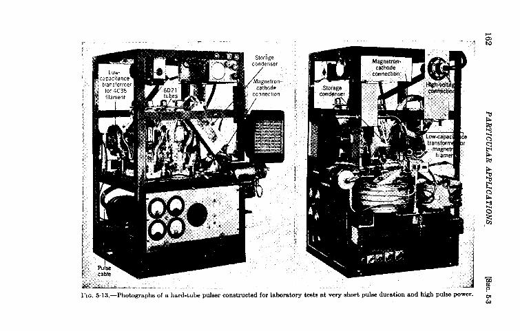
162r ~P
AR
TIC
UL
AR
AP
PL
ICA
TIO
NS-
[SE
C
..-—
T.
.,.+,~”,
:.5.3
wEl

SEC. 5.3] A HIGH-POWER SHORT-PULSE HARD-TUBE PULSER 163
The storage capacitance used for this pulser consisted of two 0.05-pf15-kv condensem connected in series. The effective capacitance of 0.025pf was ample for the short pulse durations, since the drop in voltage isonly 140 volts for a O.l-psec 35-amp pulse. These condensers werearranged so as to keep the connections short and the stray capacitanceto ground low, as may be observed in the photographs of Fig. 5.13.
One of the most serious problems encountered in the design of thispulser was the choice of a satisfactory switch tube. The requirements ofhigh pulse voltage and high pulse current could not be met by a singletube of any available type. It was necessary to choose the 6D21 tetrodefrom the standpoint of the high plate voltage needed, and to use four ofthese tubes in parallel in order to obtain the plate current required forthe maximum pulse-power operation. The curves of Fig. 3.10 indicatethat four 6D21 tubes are capable of a total plate current of 70 to 80 amp,which is sufficient to allow the voltage pulse to rise at the rate of 3000kv/psec for a stray capacitance of about 20 pgf.
In order to minimize the inductance in the pulse circuit, the plateterminals of the four 6D21 tubes were interconnected by means of athick brass plate. This brass plate served also as the mechanical supportfor one end of the storage condenser in order to provide a short connectionand to keep the capacitance to ground small. The other terminal ofthe storage condenser was attached to the magnetron-cathode terminalas can be seen in Fig. 5.13. The inductance of the ground connection tothe cathodes of the four 6D21 tubes was also kept small by mounting thesockets on a heavy brass plate that served as the common ground ter-minal for the pulser circuit.
The low value of stray capacitance across the pulser output aided thequick return of the pulse voltage to zero at the end of the pulse. Inorder to make the voltage fall to zero in a few hundredths of a micro-second, however, it was still necessary to use a relatively low resistancefor the storage-condenser recharging path. A value of 2000 ohms wasused, although this value was only about twice the normal load resistance.The use of an inductance for the recharging path was not considered,because it would then be necessary to add a shunt diode to eliminate thebackswing voltage, and the addition of such a diode to the circuit wouldof necessity increase the stray capacitance. It was considered moreimportant to keep this capacitance small than to decrease the pulse powerlost in the shunt path by the use of an inductance.
The Driver Circuit. —Because of the relatively large pulse powerrequired to drive the grid of four 6D21 tubes, it was decided to use apulse-forming network driver of the type discussed in Sec. 4“3. Thisdriver was a line-type pulser using inductance charging of the pulse-forming network. A hold-off diode was used in the network-charging

164 PARTICULAR APPLICATIONS [SEC.53
circuit in order to provide some flexibility in the range of pulse recurrencefrequencies that could be used. The circuit was so arranged that thescreen-grid voltage for the 6D21 tubes was obtained from the powersupply used to charge the network.
The pulse-forming network in this driver consisted of a short lengthof 50-ohm high-voltage pulse cable. The pulse duration could then beeasily changed by varying the length of the cable. The lengths actuallyused for various pulse durations were obtained experimentally, and areindicated in the diagram of Fig. 5.12. The approximate length to beused for a particular pulse duration can be calculated since it is knownthat the velocity of propagation for a voltage wave in this cable is about45o ft/~sec and that the wave must traverse the length of cable twiceduring the pulse. The coil of cable used for the pulse-forming networkmay be seen in the photograph of Fig. 5.13.
In order to obtain a fast rate of rise for the pulse applied to the gridsof the 6D21 tubes, it was necessary to keep the connection between thedriver and the grid terminals as short as possible. The 4C35 switch tubeof the driver was therefore mounted upside down beneath the plate sup-porting the four tubes. Since the cathode of the 4C35 must rise and fallin potential along with the 6D21 grids, a low-capacitance transformer wasused to supply the cathode-heating power.
Operation. —This pulser was operated at pulse durations as short as0.02 usec and at a pulse power of 950 kw with a magnetron load. Themagnetron pulse current was not observed in the usual way (see AppendixA), in which a resistor is introduced between the magnetron anode andground, because for these short pulses the added capacitance and induct-ance introduced b.v such a resistor was sufficient to cause distortion ofthe pulse shape. “The pulse current was determined from the measuredaverage magnetron current, the pulse recurrence frequency, and thepulse duration. The pulse duration was measured for the r-f envelopepulse, and the oscilloscope sweep speed calibrated by measuring thefrequency difference between the first minima on either side of the centerfrequency of the r-f spectrum. This calibration was done with a O.l-psecpulse whose frequency difference of 20Mc/sec could be measured withreasonable precision.
Photographs of the oscilloscope traces for some voltage and r-f pulsesobtained with this pulser are reproduced in Fig. 5“14. The time delaybetween the start of the voltage pulse and the start of the r-f pulse ischaracteristic of magnetrons, and its magnitude depends on a largenumber of factors (cf. Chap. 9 of Vol. 6). The relatively slow rate ofrise for the r-f envelope pulse is due in part to the detector and the oscillo-scope circuit used to obtain the trace. The fraction of the observed timerequired for the r-f pulse to build up that was due to the circuit and the

SEC. 5.4] APPLICATION OF PULSE-SHAPING NETWORKS 165
fraction that was inherent in the magnetron output were not determinedin these cases. Other experiments’ have indicated that the time for thisbuildup may be about 0.01 psec.
One of the interesting results obtained with this pulser is the factthat a magnetron can operate satisfactorily with considerably higherpulse-power input as the pulseduration is decreased. With a725A magnetron, for example, theoperation ~vas satisfactory, thatis, there was no sparking, \vith apulse-power input of 900 kw at a
pulse duration of 0.03 ~sec. Ther-f power output under these con-ditions was 195 kw. In contrast,the magnetron could not be oper-ated above 15 kv and 15 ampwithout sparking ~vhen the pulseduration ~vas about 2 psec.
5.4. The Application of Pulse-khaping Networks to the Hard-tube P u 1s e r .—Throughout thepreceding discussions of the designof hard-tube pulsers, the effect ofthe value of the storage-condensercapacitance on the change in pulsevoltage and pulse current during a
Voltage pulse r-f pulse(a)
Voltage pulse(b)
Fro. 5 14.—Photographs of oscilloscopetraces for voltaee and r-f nulses obtainedwith a high-po-wer short-~ulse bard-tubepulser. (a) 0,1 gsec pulses, (b) 0.03 psec pulses.
pulse is emphasized. It is shown in Chap. 2 that, if the time constant forthe discharging circuit of the storage condenser is large compared with thepulse duration, the drop in pulse voltage during the pulse is given approxi-mate] y by the relation AVI = llr/CW. If the pulse voltage changes, thepulse current also changes, but, as indicated in Chap. 2, the above relationis a sufficiently good approximation when AV1 is only a small percentageof the pulse voltage.
When the load on a hard-tube pulser is a pure resistance,
A1 A~.I v.,:m.,
where Z~.1 and V~., are the maximum load current and voltage at thebeginning of the pulse. With a magnetron or biased-diode load thedynamic resistance is generally only a small fraction of the static resist-ance, and AI/In.. > AV/ V~=, the inequality becoming larger as the
1F. F. Rieke and R. C. Fletcher, “Mode Selection in Ifagnetrons, ” RL ReportNo. W9 Sept. 28, 1945.

166 PARTICULAR APPLICATIONS [SEC.5.4
dynamic resistance becomes smaller, In some cases the magnitude ofthe current change may be so large that the operation of the magnetronoscillator is unsatisfactory. For given values of Z1and T the magnitudeof AV can be decreased by increasing C., but the resulting increase incondenser size becomes a serious problem when the size and weight ofthe completed pulser are important. The purpose of the present discus-sion is to point out a method for reducing the change in load currentduring the pulse without increasing the storage capacitance. Themethod consists of adding a network in series with the discharging circuitof the storage condenser. The network may be simply a resistance andan inductance in parallel, or it may be a more complex combination ofresistance, inductance, and capacitance.
In order to indicate the effect of such a network on the load currentduring the pulse, an example in which the network consists of an induct-ance, L, and a resistance, R, in parallel is discussed in detail. The fol-lowing discussion deals only with the load current associated with thetop of the pulse, so the output circuit of the pulser may be simplified byneglecting the stray capacitance and inductance inherent in any design.The circuit is further simplified by considering an ideal switch with its
~ effective resistance combined in the load re+- Ri
a
T
sistance. The analysis is made for the circuitc. = shown in Fig. 5.15 with a pure-resistanceL iz
load. The initial voltage on the storageST R; condenser is Vw, and the current in L is
Ii assumed to be zero before the switch & isclosed in order to start the pulse. The re-
F1o. 5.15.—Simplifiedout-Put circuit of a hard-tube
sistance R; includes any resistance in series
pulser with an LR-network to with the pulse circuit exclusive of that intro-
minimize the change in load duced by the network. Thus R{ representscurrent during the pulse.
the effective resistance (RJ + TP) for a resist-ance load Rl and a switch tube of resistance Tp. Using Kirchoff’s laws,the Laplace-transform equations for this circuit are
~@) = ~wRi,(p) + R;~z(P) + ~ p Y (1)
Ri,(P) + LPi2(P) = 0, (2)and
ii(p) + iz(p) = 12(p). (3)
An equation for Ii(p) is obtained by combining Eqs. (l), (2), and (3),with the result
v.(R + R;) ()
p+:I,(p) =
RR;Cw -1-L R“(4)
‘2 + (R + Rj)LCw p + (R + R;)LCw

SEC. 5.4] APPLICATION OF PULSE-SHAPING NET WORZiS
LetRR;Cw + L
% = (R + R;)LC.
andR
b = (R + R;)LC.”
Then Eq. (4) may be written
v. () R
~,(p) = (R + R;) p + ~
(p+a)’+u’ ‘
where Oz = b — a2.
The inverse Laplace transformation of Eq. (7) gives
If b < az, let kz = –uz = az – b. Then
~it) = (R ~R;) [ 1e-”’ cosh kt + ‘R ~kLa) sinh kt .
If b = az,
167
(5)
(6)
(7)
(8)
(9)
(lo)
(11)
These three equations give the load current as a function of time for anycombination of the circuit parameters. Since in most pulser designs thetime interval involved is very small, the point of interest is whether ornot a condition can be found for the circuit parameters such that I(t)is aslowly varying function near t = O. This condition can be determinedby differentiating Eqs. (9), (10), and (11) with respect to time and equat-ing the derivative to zero. Thus from Eq. (9)
dIl
— = (R FR;) ‘-a’dt [-U sin d + ‘R ~La) cos d - a Cosd
a(R – La) sin tit—Lu 1
(12)
Equating this derivative to zero for t = O gives the condition
R = 2La. (13)
With the value of a from Eq. (5), Eq. (13) becomes
L = R2Cw. (14)

168 PARTICULAR APPLICATIONS [SEC. 5.4
The identical condition is obtained by carrying out the same procedurewith Eqs. (10) and (11). If the relation of Eq. (14) is used, Eqs. (9),(10), and (11) become
t——11(0 = (R yR{)
(
1e ZRcW cos d + —
2RC.W )sin d , (15)
——11(0 = (R “fiR{)
(e Zic- cosh kt + &k
)sinh kt , (16)
wand
‘t(t) = (R ~R;)+(”a” (17)
Thus, when the condition of Eq. (14) is satisfied by the components of theLR-network, the plot of load current as a function of time has a zero slopeatt=O. The equation for the load current without the LR-network inthe pulser output circuit is
v. e-&.11(0 = ~ (18)
Since the plot. of current versus time from this equation has a slope notequal to zero at t = O, the decrease in load current obtained from Eqs.(15), (16), and (17) should be less for small values of tthan that fromEq. (18).
A numerical example shows more specifically the effect of the LR-net-work on the change of load current during the pulse. Assume thefollowing values for the circuit parameters for Fig. 5.15:
Vm = 12.5 kv.R! = 1000 ohms.Cw = 0.05 pf.R = 50 ohms.L = R2Cw = 125 ph.r = 1 psec.
If L = RZC~ is substituted in Eqs. (5) and (6), Eq. (8) becomes
3R – R;
‘2 = b – a’ = 4R2C:(R + R;)”
In the present example, 3R < R;, so
k2=a2–b= R; – 3R
4R2C~(R •1-R;)’
and the current is given by Eq. (16). The change
(19)
(20)
in current during

SEC.5.4] APPLICATION OF PULSE-SHAPING NETWORKS 169
1 psec is theref ore
AI1 = 12”~O&108 [1 – e-o’ (cosh 0.18 -1-1.1 sinh 0.18)]
= 11.9 X 0.005 = 0.06 amp.
Without the LR-network, the change in load current obtained from Eq.(18) is
All = 12”~o~010’[1 – e-o”’]
= 12.5 X 0.02 = 0.25 amp.
Using the approximate calculation
voltage is
AVl = ~5 = 250 volts,
andAIl = ~~ = 0.25 amp.
AV1 = $ T, the change in pulsew
V.t+- R
6-”/.,’-” p,
I {<Thus the droop in the current pulse is de-creased by a ~actor of four wh& the LR-
network is inserted. ~“If the load is a biased diode or a magnetron, Fm. 6.16.-SimpliSedout-
the output circuit of the pulser appears as ~~tm~tic~~h‘~ ~ia~d~ifi~shown in Fig. 5.16. The analysis for this load and an ZX-netw.rk tocircuit is identical to that for the circuit minimizethe changein load
current during the pulse.of Fig. 5.15, T{ replacing R; and Vw – V,
appearing in place of Vw. The resistance T; represents the sum of thedynamic resistance of the biased diode and the effective switch-tuberesistance, that is,, (T1+ T,). As another numerical example indicatingthe effect of the LR-network, consider the following values for the circuitparameters:
Vw = 12.5 kv.V, = 10 kv.Cw = 0.05 pf.l’; = 200 ohms.
R = 50 ohms.L = R2Cu = 125 ph.T = 1 psec.
Since r; > 3R, Eq. (16) again applies, and the change in load currentduring 1 psec is
AIl = ~ [1 – e-o’ (cosh 0.089 + 2.2 sinh 0.089)]= 10 X 0.015 = 0.15 amp.

170 PARTICULAR APPLICATIONS [SEC. 5.4
Without the LR-network, the change in current according to Eq. (18) is
AIz = ~ (1 – e-o.’) = 12.5 X 0.095 = 1.19 amp.
Using the approximate calculations for AV,
12.5— = 250 volts
‘V1 = 0.05and
AIl = $= = 1.25 amp,
which agrees reasonably well with the value of 1.19 amp calculated bythe exact relation of Eq. (18).
‘;:q%%s~qpsCircuitA CircuitB ‘
0.9%??
0.8 \ \4
0.7@
1,t?)‘%~
0.6+
0.5Circuit
B
0.4-\’
0.30 2 4 6810
t infi secalter clwing ST
FXQ. 5.17.—Change in load current as a function of time with and without an LR-networkin series, with the output circuit of 8 hard-tube pulser.
In order to keep the load current constant within 0.15 amp by increas-ing the capacitance of the storage condenser, this capacitance has to beabout 0.4 pf. It is therefore evident that a significant advantage resultsfrom the use of the LR-network in series with the discharging circuit ofthe storage condenser. If the allowable drop in the load current is largerthan the values obtained in the above examples, the use of an LR-net-work makes it possible to have a smaller capacitance for the storagecondenser.

SEC.5.4] APPLICATION OF PULSE-SHAPINf7 NETWORKS 171
The general effect of the addition of the network on the load current isindicated by the curves of Fig. 5.17. One set of curves is given for a900-ohm resistance load, and another set for a biased-diode load with a100-ohm dynamic resistance, the switch-tube resistance being 100 ohmsfor each set. These curves show that a marked improvement in the slopeof the top of the current pulse can be obtained even for relatively longpulse durations. The curves also indicate that the use of an LR-networkis more important in the operation of the pulser with a low-resistanceload.
The examples given above indicate that there is also a disadvantageassociated with the use of the LR-network. The presence of the resist-ance R in series with the load results in a lower pulse current for a givencondenser voltage V.. For the resistance load, the maximum value ofthe pulse current is 12.5 amp without the network and 11.9 amp with thenetwork. For the biased-diode load, the corresponding current valuesare 12.5 amp and 10 amp. Thus, the pulse power delivered to the biased-diode load having a dynamic resistance of 100 ohms is 110 kw with theLR-network, and 141 kw without it. In order to obtain the same pulsepower in the load in both cases, it is necessary to increase the condenservoltage from 12.5 kv to 13.1 kv when the network is used. The actualpower loss in the resistance of the LR-network is small (about 5 kw in theexample given here), but the requirement of a higher condenser voltage issometimes an inconvenience. In the design of a hard-tube pulser, it istherefore necessary to weigh the reduction in pulse power or the increasein condenser voltage against the drop in load current during the pulse oran increase in the capacitance of the storage condenser.
FIG. 5.lS.—Output circuit of a hard-tube pulse. with a network of passive elements tomaintain approximately constant load current during the pulse.
Another method by which the pulse current can be kept approximatelyconstant for pulse durations of about a microsecond is indicated in thediagram of I’ig. 5.18. This arrangement was first suggested to membersof the pulser group at the Radiation Laboratory by Mr. A. A. Varela ofthe Naval Research Laboratory, Anacostia, D.C.

172 PARTICULAR APPLICATIONS [SEC.5.4
This arrangement has an advantage over the LR-net.work in that thenetwork consists of passive elements. There is, however, a loss in pulsevoltage, which makes it necessary to charge the condenser Cw to a highervoltage than is required without the network for a given pulse voltage atthe load. Another possible disadvantage of this arrangement is the needfor three circuit elements, including a condenser with a relatively highvoltage rating.

PART II
THE LINE-TYPE PULSER,The general characteristics of line-type pulsers are given in Sec. 1.4,
and a comparison of some features of the two principal types of pulsersare made in Sec. 1.5. The next six chapters of this volume present adetailed discussion of the line-type pulser. Before going into the analysisof the components and circuit behavior, it is well to summarize the generalphilosophy from which the line-type pulser has been developed.
Fundamentally, the pulser consists of a reservoir of electrical energythat is allowed to discharge completely into a load at predeterminedtimes to form the pulses, and that is connected to a source in such a waythat the same amount of energy is stored in it during each interpulseinterval. Obviously, there are many types of energy reservoirs that areunsatisfactory because the rate of discharge of their energy into the loaddoes not produce the desired pulse shape. Chapter 6, dealing with pulse-forming networks, sets forth the analysis by which combinations ofinductances and capacitances are determined to approximate a specificoutput pulse shape, and gives the results obtained by various methods ofanalysis for the pulse shapes most commonly used in pulsers for micro-wave radar. The pulse-f orming networks have been derived by con-sidering circuits that do not include losses, or stray capacitances andinductances, and for which the load resistance is equal to the networkimpedance. The effects on the output from the pulser of nonlinear loads,of impedance mismatch between load and network, of losses and of straycapacitances in the circuit are considered in Chap. 7.
Chapter 8 gives a discussion of the types of switches most commonlyused with line-type pulsers, and of the auxiliary circuits that they require.The different methods of restoring the energy to the pulse-forming net-work between pulses are considered in detail in Chap. 9, and the over-allperformance of the pulser as it is affected by the various components andby variations in load impedance is discussed in Chap. 10. Finally, Chap.11 gives a few examples of pulsers in use at present, and also indicatesthe possibilities of some variations in the usual pulser circuit.
It is worth noting again that the fundamental circuits of line-typepulsers are always very simple. There can be many variations, depend-ing on the required polarity of the output pulse and the power supplyavailable. Possibly their greatest advantage, next to their inherent
173

174 THE LINE -T YPE PULSER [SEC. 6.1
simplicity, stems from the fact that only sufficient energy for one pulse isstored at any one time; by comparison, the energy stored in the reservoirof the hard-tube pulser is nearly always twenty to fifty times that requiredby the load for a single pulse. The possibility of damage to the load orto the pulser is thus naturally greater with a hard-tube than with a line-type pulser.
The circuit simplicity results in less flexibility than can be obtainedfrom hard-tube pulsers. The latter type can usually be altered withlittle effort to satisfy new requirements of pulse duration and recurrencefrequency. In the present state of development, a line-type pulserrequires a new pulse-forming network if the pulse duration is to bechanged and, in the case of a-c charging of the network, it is also inflexibleas to recurrence frequency.

IL!ulq>
CHAPTER 6 cl?k-
THE PULSE-FORMING NETWORKr]
0BY H. J. WHITE, P. R. GILLE~”E, AND J. V. LEBACQZ1 (:)
The pulse-forming network serves the dual purpose of storing exac~ ““$&the amount of energy required for a single pulse and of discharging t
energy into the load in the form of a pulse of specified shape. ~herequired energy may be stored either in capacitances or in induct
Networks in which thF&T”~in combinations of these circuit elements.. .
is stored in an electrostatic field are referred to as voltage-fed net~~’ ~networks in which the energy is stored in a magnetic field are refer~tew *as current-fed networks. Networks of the voltage-fed type are -:?
dalmost universally in practice because only with this type can the ‘“~j~gaseous-discharge switches, such as spark gaps and thyratrons, be
@
K---
The current-fed networks have certain important advantages, but #
far no suitable switch is available that permits high-power oper “ .U
Therefore, the discussion of networks is confined largely to the consl“~H
tion of the voltage-fed type.6.1. The Formation and Shaping of Pulses. Determination of
Pulse-forming Networks for Generating Pulses of Arbitrary Shape.—A general mathematical procedure exists for the determination of pulse-forming networks to generate pulses of arbi- Puls&~l#gtrary shape, and the outlines of the theory aregiven for the case of voltage-fed networks.
-
Pul=shapingIf it is assumed that all the energy is stored in nelwork
C//one condenser, the pulse-generating circuit ZNtakes the fotm of Fig. 6.1. The required cur-
}Witch RI
rent pulse i(t) flowing in the circuit may bearbitrary in shape but practical considerations ~
6.1.—Basic circuit! limit it to finite single-valued functions hav- ~0,~e~eratil,~~d=~ .f ~rbi-
ing a finite number of discontinuities and a trary shape (voltagefed
finite number of maxima and minima. In ‘etWork)”analyzing this problem the Laplace-transform method is used. Thetransform for the current may be found from the definition of the Laplacetransform, and is
/
.i(p) = ~ i(t)e–p~ dL (1)
1Section6.5 by P. R. Gillette,Sec. 6.6 by J. V. Lebacqz, the remzinderof Chap. 6by H. J. White.
17s

176 THE PULSE-FORMING NETWORK [SEC.61
The Laplace-transform equation for the circuit of Fig. 6“1 is
( ) v.R1+ZN++P i(P) =&p=~J (2)
where R; is the load resistance, ZN is the network impedance, CN is thenetwork storage capacitance, and QN is the initial charge on the network.The amplitude of i(p) is determined by V., the initial voltage on CN. Forthe present, VN may be considered as a known constant, and Eq. (2)may be solved explicitly for the unknown impedance of the network,giving
VNzN=-
1–R1–fi.
pz(p)(3)
As a simple illustration, suppose that the current pulse is specified asbeing rectangular with amplitude 12and duration r, and that the load is apure resistance of value R1. Then i(p) is found from Eq.(1) to be
i(p) = ; (1 – ~–q .
Substituting in Eq. (3), there is obtained
ZN =pvx
pZl(l – e-~) –or rearranging,
R, – &,
If the numerator and denominator are multiplied by e~iz,
Choosing VN = 2Z&1, there is obtained
Z. + &p= Rl coth ~ (4)
The right-hand member of Eq. (4) is recognized as the impedancefunction for an open-circuited lossless transmission line of characteristic

SEC.6.1] THE FORMA TION AND SHAPING OF PULSES 177
impedance 20 = RI, and transmission time 6 = 7/2. Hence, in thiscase, either the pulse-shaping circuit plus the capacitance CN must be anelectrical equivalent for the transmission line, or the transmission lineitself may be considered as one form of the network that generates therequired rectangular pulse.
Unfortunately, in all but the simplest cases it proves very difficultto recognize an actual physical network from the form of ZN given byEq. (3), and there is no straightforward method for changing the expres-sion into a form which is so recognizable. The difficulty is increased bythe fact that ZN generally contains dissipative as well as reactiv e elements.Hence, actual designs are usually based on more specialized and indirectapproaches to the problem, the most important of which are discussedbelow.
Pulses Generated by a Lossless Tran.wnis-
w“on Line.—Since the microwave oscillatorsfor which most pulsers have been designedrequire the application of an essentially rec-tangular pulse, the lossless open-ended trans-mission line considered in the foregoing examplemay be taken as a starting point in the discus-sion. The nature of the transient produced by
ho 1 !
FIG. 6.2.—Schematic cir.cuit diagram for producing anideal rectangular pulse froma transmission line.
the discharge of such a transmission line into a resistance bad (see Fig.6.2), may be studied in more detail by further application of the Laplacetransform or operational method of analysis.
The a-c impedance, Z, of the transmission line, is given by elementarytransmission line theory as
Z = 20 coth ju&.
The Laplace-transform impedance is foundwhere p is the transform parameter. Then
Z(p) = Z, coth pa,
by substituting p for ju,
(5)
where 6 is the one-way transmission time of the line, and 20 is its charact-eristic impedance. The current transform is then
v,~b)= P(RL + 20 coth P~)
Vo 1 – e–2d‘p(Zo+RJ)”l+~
20 + R1@P6
= V3(1 – e-’~)
[ ()
zo– R12e-4ti _.. . , (6)Z, – R1 e-,ti ~ —p(zo + 2?1) l–ZO+R1 ZO + R1 1

178 THE P ULS’E-FORMING NET WORK [SEC. 6.1
where VO is the initial voltage on the transmission line. The inverse
transform gives the current as
v, ( Zo – RI [u(~ – 26) – U(t – 4~)1‘(t) = Z. + R1 1–u@-2@-zo+R2
()+ W’[u(t–4a)–
IU(t–66)] –... , (7)
wheret7(At) = 1 for At >0.?7(At) = O for At<O
At = (t – n~), n = 2,4,6, . . . .
If Rl = 20, that is, if the line is matched to the load, the current con-sists of a single rectangular pulse of amplitude 11 = VO/2Z0 and duration~ = 28. Current and voltage pulses for Rl = 20, Rl = 2Z0, and R; = ~ZO
are shown in Fig. 6.3.
~LO 10 26
L
L---! ---
!-------
0 26 46 66 86
(a) RI =Zo (b) Rl = 2Z0
I---
0;
~----
-F-6 46 bii ‘---”86
L---J
FIG. 6.3.—Current and voltage pulees for a losslees transmission line discharging intoa resistance load. The solid and broken lines represent the voltage and current pufsas,respectively.
The effect of mismatching the load is to introduce a series of steps into
the transient discharge. These steps are all of the same sign when
Rz >20, and alternate in sign when RI <2.. An elementary explanationof the steps can be made in terms of reflections caused at the terminals ofthe line by mismatching the load resistance. These reflections traversethe line to the open end in time 6, are completely reflected there, andtravel back to the load end in a total time 26, where they appear as posi-

SEC. 6.2] NETWORKS DERIVED FROM TRANSMISSION LINE 179
tive or negative steps depending upon the mismatch ratio. The reflec-tions continue in this way, with constantly diminishing amplitude,until all the energy initially stored in the line is dissipated in the loadresistor. Both the design and operation of line-type pulsers are affectedby these reflections.
A transmission line having a one-way transmission time of 8 generatesa pulse of duration 26; assuming a pulse of l-psec duration and a signalvelocity on the line of 500 ft/psec (a representative value), a line of length1 = 500 X 1/2 = 250 ft is required. It is obvious that a high-voltageline or cable of this length would be impractical because of its large sizeand weight, and hence, that a substitute in the form of a line-simulatingnetwork is necessary for any practical equipment. Pulse-forming net-works have other advantages in that the pulse shape may be altered byvarying the values of the network parameters and the number of elements.
6.2. Networks Derived from a Transmission Line.-The develop-ment of pulse-forming networks that simulate a transmission line is amathematical problem in network synthesis. As may be anticipated, nonetwork having a finite number of elements can exactly simulate a trans-mission line which in reality has distributed rather than lumped param-eters. As the number of elements for a given network type is increased,the degree of simulation will improve. It may happen, however, thatthe network pulse is a good approximation to the rectangular pulse duringonly a portion of the pulse interval. For example, the network pulse mayexhibit overshoots and excessive oscillations, especially near the beginningand end of the pulse. These possibilities must be kept in mind, and theproperties of networks derived by formal mathematical methods must beinvestigated with care to determine how closely the networks approxi-mate transmission lines.
Network Dem”ved by Rayleigh’s Principle. —From the mathematicalpoint of view, physical problems involving distributed parameters giverise to partial differential equations, whereas lumped-parameter problemsgive rise only to ordinary differential equations. Inasmuch as thepartial differential equation for a physical problem may usually be derivedby taking the limit of a set of ordinary differential equations as the num-ber of equations in the set approaches infinity, 1 it is clear that a finitenumber can at best give only an approximate answer to the distributed-parameter problem, but that the degree of approximation improves asthe number of equations, and therefore the number of physical elements,is increased. This line of reasoning also appears plausible on purelyphysical grounds.
1Usually referredto as Rayleigh’s principle. See, for example, A. C,. Webster,Partial Differential Equatiom of Mathematical Physics, 2nd cd., Stechert,New York,1933,pp. 93-97.

180 THE PULSE-FORMING NETWORK [SEC.6.2
Application of Rayleigh’s principle to the transmission line yields thetwo-termirml line-simulating network shown in Fig. 6.4.
The properties of the line-simulating network of Fig. 6.4 may con-veniently be investigated by find-
Linesimulatmgnetwork ing its impedance function. Forpresent purposes the operator func-
m~RLj impedancefunctioTheStion is used rather than the a-c
alternative forms are equivalent,~ ~ but the operator form is particu-
larly useful in calculating the tran-.- sient response.
FIG.6.4.—Two-terminalline-simulatingnet- The impedance function mayworkderivedby Rayleigh’aPrinciple.
be found by writing down the setof n transform equations for the network and noting that these are differ-ence equations, each equation except the first and last being of the form
-W+(’’+ar’’’-w=o (8)
where r is the rth mesh. The general solution of this difference equationis
i,(p) = Ae’” + Be–’e (9)
where cosh o = 1 + (LC/2)p2, and A and B are arbitrary constants tobe determined by substitution in the first and last mesh equations. Con-sider first the case for which the resistance RI, in series with the batteryv~, is put equal to zero. The circuit is then composed of purely reactiveelements, and the currents that flow upon closing the switch persist—that is, the currents continue indefinitely and represent a steady-staterather than a transient condition. Transients can arise only if dissipativeelements are present. Solving for the arbitrary constants A and B andreducing to hyperbolic functions, the following expression is obtained forthe current transform i,(p):
sinh nOii(p) = CVN
sinh (n + 1)0 – sinh nO”
The corresponding input-impedance transform for the network is then
Z(p,n) = a = ~[ 1
1 sinh(n+l)o_l.sinh (no)
(lo)
It maybe of interest to find the limiting form of Z(p,n) as n approachesinfinity in such a way that the total inducts.nce and capacitance of thenetwork remain constant.

81JC.6.2] NETWORKS DERIVED FROM TRANSMISSION LINE 181
n4 m
But
Cosho=
sinh O =
no =
which f@eS
[
1 sinh (n + 1)0 _ ~h ‘@’n) = n:m. Gp sinh (ntl) 1
~ [cosh O + coth no si.nh O – 1]= J5n CP
LC LNCN ,l+~P’=l+7j--#-P!
mdc05h*e-l=—
n pm
( –p)]=&.~L.CNcoth 2n sinh-l ~ coth p GN
= ZH coth pa, (11)
whioh is the exact form for the impedance function for a transmissionline given in Eq: (5). Thus, the network impedsnce function reduces inthe limit to the transmission-line impedance function, in accord withRayleigh’s principle.
The pulse shape generated by the line-simulating network of Fig. 6“4on matched resistance load, Rl = - = ~C, may be found bycalculating the charging-current pulse when the voltage VN is applied tothe circuit of Fig. 6.4. If the voltage transform is divided by the sum ofthe load resistance and the network impedance [Eq. (10)],
VN—
“(’)‘++i[sin~i$:,’)e-11w.=
[ 1
;PVTc+ sinh (n + 1)0 _ ~
sinh m?
but from the value of o in Eq. (9)
——p-~sinh:,
ii(p) = Cvh. sinh ntl
( )
) (12)
sinh (n + 1)0 + 2 sinh ~ – 1 sinh” nt?

182 THE PULSE-FORMING NETWORK [SEC. 62
Equation (12) is valid for any number of sections n. The simplestcase occurs when n. = 1, that is, when the network is reduced to a singlemesh. In this case
sinh oii(p) = Cv,v
( )sinh 26 + 2 sinh ~ — 1 sinh o
Cv.v.
2cosh0+2sinh~–1
w.
‘2+ Lcp’+mcp–l
v. 1—— —.L
J
P’+*CP+*
which is recognized as the current transform for a one-mesh RLC-circuitwith R = ~L/C.
By the method used in deriving Eq. (11), the limit of i,(p) as napproaches infinity in such a way that the total distributed capacitanceC. and the total distributed inductance L. remain fixed is shown to be
lim i,(p) = ‘JM (1 – e-’-p),n+ =a
J2 Gp
(13)
This is the Laplace transform for a rectangular current pulse of amplitude
v.
2 4LN/CN
and of duration 2 m, and is the result to be expected according toRayleigh’s principle.
In order to check the theory, both calculated and experimental pulseshapes were obtained for a five-section uniform-line network on matchedresistance load, that is, when R1 = ZN. The calculated pulse shape wasfound by using Eq. (12) with n = 5. In carrying out the solution, it isnecessary to convert from the hyperbolic to the algebraic form corre-sponding to Eq. (12). Since the denominator is of the 10th degree ( = 2n),the roots are tedious to find. The resulting pulse shape is plotted inFig. 6.5a, using dimensionless ratios for the coordinates. The corre-sponding experimental pulse shape, shown in Fig. 6.5b, was obtained byusing an experimental network for which the actual values of all theparameters were within 1 per cent of the theoretical values. The cor-respondence between the calculated and experimental pulse shapes is

Bxc. 6.2] NET WORKS DERIVED FROM TRANSMISSION LINE 183
very close, the only significant difference being in the initial overshootfor which the calculated value is about twice the observed value. Thisdifference occurs probably because the hydrogen-thyratron switch usedin the experimental pulse-generator circuit does not close instantaneously,and also because there are, in any physical system, unavoidable lossesand distributed capacitances and inductances.
A
(a) Calculated puke. (b) Observed puke.
Fm. 6.5.—Pulse shapes produced by a fiva-eaction uniform-line network on matchadresistance load.
(a) RI = ZN. (b) RI = 2ZN.FIG. 6.6.—Voltsge Pukw shapas obtained with the network of Fig. 6.5 as aean with a slow
aweep apaad.
The oscillograms in Fig. 6.6 were taken with the same network;Fig. 6“6a is identical with Fig. 6“5b except that a slower sweep speed wasused in order to show the complete pulse tail. The effect of mismatchwith Rl = ZZN is shown in Fig. 6.6b, in which the series of steps as shownin Fig. 6.3b is evident, although not very well defined. It may be con-cluded that the five-section uniform-line network is a poor equivalent fora transmission line. A larger number of sections would give better line-simulation, but this approach is not a very promising one.
Relation to Steady-state Theory.—The network of Fig. 6.4 comprises alow-pass filter for alternating sine-wave currents. The correspondencebetween its transient d-c pulse properties and steady-state sine-waveproperties is of considerable interest. For steady-state sine-wave cur-rents, the solution of the network is of the same form as Eq. (9), that is,

184 THE PULSE-FORMING NETWORK [SEC. 6.2
for the rth meshi,(t) = A e’” + Be–’o, (14)
where Ois now defined by the expression
cosh e = 1- L+. (15)
Equation (14) shows that i,(t) will be attenuated only if Ohas a nega-tive real component, that is, if
e=. +jp and a<O
Then, as cosh 0 can be expressed in the form
cosh e = cosh a cos iil – j sinh a sin b,
it is clear that, for a = O,cosh a = 1, sinh a = Oand cos d = 1 – LCQ2/2.Inasmuch as cos P must satisfy the inequality Ices PI S 1, there results
LCW2l-~sl,
or
(16)
Thus all frequencies, O S f S l/r ~, are passed without attenua-tion, whereas all higher frequencies are increasingly attenuated.
The Fourier series for a succession of identical and uniformly spacedrectangular pulses contains discrete frequencies extending throughoutthe band to infinity. Most of the pulse energy is accounted for, how-ever, in the frequency band between zero and several times 1/?. A veryconservative estimate for the significant upper frequency limit might betaken as 10/,. Thus, it is reasonable to set the cutoff point for the low-pass filter that will transmit such rectangular pulses without appreciabledistortion as
10f.=& =7,
or
(17)
The quantity m represents the delay time per section of the low-pass filter; therefore, an n-section filter structure, when used as a pulse-generating network, should produce a pulse of duration
r=2n~. (18)
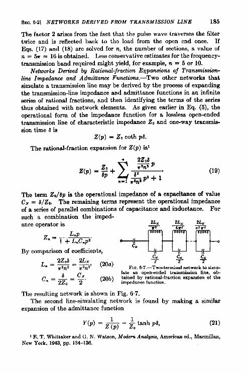
SEC. 6.2] NETWORKS DERIVED FROM TRANSMISSION LINE 185
The factor 2 arises from the fact that the pulse wave traverses the filtertwice and is reflected back to the load from the open end once. IfEqs. (17) and (18) are solved for n, the number of sections, a value ofq~=~= 16 is obtained. Less conservative estimates for the frequency-transmisaion band required might yield, for example, n = 5 or 10.
Networks Derived by Rational-fraction E4paw”ona of Transmission-
liw Impedance and Admittance Functions.-Two other networks thatsimulate a transmission line may be derived by the process of expandingthe transmission-line impedance and admittance functions in an infiniteseries of rational fractions, and then identifying the terms of the seriesthus obtained with network elements. As given earlier in Eq. (5), theoperational form of the impedance function for a lossless open-endedtransmission line of characteristic impedance ZO and one-way transmis-sion time 6 is
Z(p) = Z, coth pb.
The rational-fraction expansion for Z(p) isl
.
z 2208~P
z(p) = * + .
n-, .$$P’+ 1
(19)
The term ZJO is the operational impedance of a capacitance of valueC. = fi/ZO. The remaining terms represent the operational impedanceof a series of parallel combinations of capacitance and inductance. Forsuch a combination the imped-ance operator is 2L~
2. = ‘“p1 + LnCnp2”
By comparison of coefficients, “cM-b
L-= ~ = ~~, (20a)
c,% % -2-
Fm.6.7.—Two-terminal network to aimu-Iate an open-ended transmimion line, ob-
c.=&=g. (~b) ~~~~a~er:~i~~ion expansion of the
The resulting network is shown in Fig. 6“7.The second line-simulating network is found by making a similar
expansion of the admittance function
1Y(P) = ~~ = ~.~ tanh p6, (21)
1E. T. Whittaker and G. N. Watson, Modem A TULZVG,Americancd., Macmillan,NewYork, 1943,pp. 134-136.
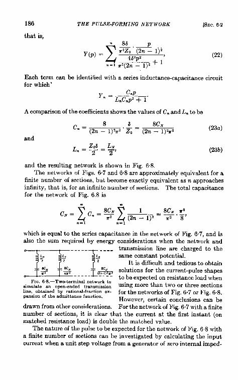
186
that is,
THE PULSE-FORMING NETWORK [SEC.6.2
.
s86 P
Y(p) =T=o” (2n — 1)2
4&p2 + ~’n=l 7f2(2~ — 1)2
(22)
Each term can be identified lvithaseries inductance-capacitance circuitfor which’
Y,, =C.p
M&p’+ 1“
A comparison of the coefficients shows the values of C’. and Ln to be
8 6 8CNc“ = (2n – 1)’7r’ “ z = (2n – l)%F
(23a)
and~ _zoa_g,
. 22(2.%)
and the resulting network is shown in Fig. 6.8.The networks of Figs. 6.7 and 6.8 are approximately equivalent for a
finite number of sections, but become exactly equivalent as n approachesinfinity, that is, for an infinite number of sections. The total capacitancefor the network of Fig. 6.8 is
cN=zc.=%z(2n:l)2 =%o%n-1 n-1
which is equal to the series capacitance in the network of Fig. 6“7, and isalso the sum required by energy considerations when the network and
FIG. 6S.-Two-terminal network to~imulate an open-ended transmissionline, obtained by rational-fraction ex-pansion of tbe admittance function.
drawn from other considerations.number of sections, it is clear that the current at the first instant (onmatched resistance load) is double the matched value.
The nature of the pulse to be expected for the network of Fig. 6.8 witha finite number of sections can be investigated by calculating the inputcurrent when a unit step voltage from a generator of zero internal imped-
transmission line are charged to thesame constant potential.
It is difficult and tedious to obtainsolutions for the current-pulse shapesto be expected on resistance load whenusing more than two or three sectionsfor the networks of Fig. 6.7 or Fig. 6.8.However, certain conclusions can beFor the network of Fig. 6.7 with a finite

!3Ec. 6.2] NETWORKS DERIVED FROM TRANSMISSION LINE 187
ante is applied to the network. This is a particularly simple calculationas each network section acts as an isolated unit, and the total current issimply the sum of the currents for the individual sections. The currentfor the rth section is
and the total current is then
n
I In4 c.i(t) = ; ~
. (2r – 1); t(2r L 1) “n 2
. — .-N
(24)r-1
IEquation (24) with n - m is the Fourier-series expansion for a
rectangular wave of amplitude ~m and period 4 m, that is,the waveform that would be obtained for the original transmission line.
The degree to which the Fourier series, Eq. (24), converges toward a
rectangular wave determines the extent to which the network simulates atransmission line. The convergence of a Fourier series is uniform in anyregion for which the original function is continuous (and has a limitedtotal fluctuation), but is nonuniform in any region containing a point of(1ordinary discontinuityy. In the present instance, the only points atwhich trouble might be expected are the points of discontinuity which
i occur at t = O and at integer multiples of t = 2 #LNCN. Hence, theconvergence of the series should be investigated near these points.Denote the sum of the series (24) by S.(t). Then, it can be shown that,at time t slightly greater than zero,
/lim L%(O+) = ~ “‘~ dO = 0.926.
nh w o
Hence the maximum instantaneous current is given by
i(c)+) =4(0.926)
r= 1.179 (25)
Thus, the current rises initially to a value about 18 per cent above thevalue that would be obtained for an actual transmission line, and at thispoint the network fails in its simulation of the transmission line. Asimilar effect occurs for t = 2- + c, where c approaches zero.An overshoot of the same type occurs when using a finite number of net-work sections. (This overshoot effect of the Fourier series near a pointof ordinary discontinuityy is known as the Gibbs phenomenon.)
It is clear then that the networks of Figs. 6.7 and 6“8 fail to give arectangular wave in that substantial overshoots occur near the beginning

188 THE PULSE-FORMING NETWORK [SEC.6.2
and end of the wave, even though the number of network sections isincreased without limit.
The response of the networks of Figs. 6-7 and 6.8 in a pulse-generatingcircuit is similar, in a general way, to their performance in the rectangularwave-generating circuit just discussed, except that a single pulse is pro-duced instead of a continuing rectangular wave. When using a largenumber of sections of Fig. 6.8 and any number of sections of Fig. 6.7, thissingle pulse exhibits the same overshoat phenomenon near its beginning,and the amplitude of the overshoot is not reduced by increasing thenumber of network sections. The pulse shapes produced on resistanceload by the networks of Figs. 6.7 and 6.8 are only approximately the
same for a finite number of sec-tions, but become identical as n ap-
proaches infinity (for an infinitenumber of sections),
The pulse shape produced bythe network of Fig. 6.7 with a finitenumber of sections haa a high initialspike because the net work has noseries inductance, consisting merelyof a series of anti-resonant .9ectionsand a series condenser, This spikeis illustrated in the experimentalpulse shape of Fig. 6.9 obtained with
a six-section network; the pulse shape is a poor simulation of a rectangu-lar pulse. The high initial current is clearly in evidence, and is followedby a series of damped oscillations. The initial current does not reach twicethe matched value as theoretically expected because of the distributedcapacitance of the load and the initial voltage drop in the hydrogem-thyratron switch used in the experi-mental pulser. In contrast, it maybe noted that the network of Fig.6%, which consists of resonant sec-tions in parallel, does have inductancein series with all the condensers. Theinitial current must therefore be zero,and there is not likely to be a highcurrent spike as long as the numberof sections is not very large. This Fm. 6.10.—Voltagepuke shape for the
premise is corroborated by the shapesix-sectionnetworkof Fig. 6.8.
of the experimental pulse of Fig. 6.10, taken for a six-section network.Figure 6.1 la shows the same pulse photographed with a slower sweep
speed; Fig. 6.1 lb shows the effect of mismatching the load resistance R1.

SEC.6.3] GUILLEMIN’S THEORY—VOLTAGE-FED NETWORK 189
In this case, RI = 2Z~, or twice the characteristic impedance of the net-work. The steps on the pulse tail are well defined, and four of them areclearly visible. A comparison of this pulse with the corresponding idealpulse that would be produced by a lossless transmission line, as shown inFig. 63b, reveals a very close similarity. Therefore, for a line-simulatingnetwork of the admittance type, it may be concluded that the generatedpulse shape on resistance load isgood for a finite, but not very large,number of sections. It has beenshown that a very large number ofsections produces overshoots on thepulse. The six-section network ap-pears to have an insufficient numberof sections to produce the optimumpulse shape, as is indicated in Fig.6.10 by the fact that the initial peakis somewhat lower than the averagetop of the pulse. An increase in thenumber of sections would be expected to bring the first peak up to theaverage top of the pulse and, for a large enough number of sections,above that average. It is, therefore, to be expected that some inter-mediate number of sections produces the optimum pulse shape.
6.3. Guillernin’s Theory and the Voltage-fed Network.-The resultsof the preceding section show that networks designed to simulate alossless transmission line have limitations of a fundamental nature. Inthe generated puke these limitations are evidenced by overshoots nearthe beginning of the pulse and excessive oscillations durhg the main partof the pulse as evidenced by Fig. 6.9. Guillemin correctly diagnosedthese difficulties as being due to the attempt to generate a discontinuouspulse by means of a lumped-parameter network. In other words, theideal rectangular pulse generated by a lossless transmission line has aninfinite rate of rise and fall, and cannot be produced by a lumped-param-eter network.
Guilleminl then argued that, inasmuch as it is impossible to generatesuch an ideal rectangular pulse by means of a lumped-parameter network,the theoretical pulse that is chosen should intentionally have finite riseand fall times. Mathematically, this condition means that the dis-continuityy in the pulse shape is eliminated, and that the Fourier series forthe generated wave has the necessary property of uniform convergencethroughout the whole region. The property of uniform convergenceinsures that overshoots and oscillations in the pulse can be reduced to
I E. A. Guillemin, “ A Historical Account of the Development of a Design Procedure for Pulse-forming Net works,” RI. Report N-o. 43, Ott. 16, 1944.

190 THE PULSE-FORMING NETWORK [SEC. 6.3
any desired degree by using a sufficient number of sections. The intro-duction of an arbitrary pulse shape leads to a new difficulty, however, inthat the impedance function necessary to produce the given pulse shapeis unknown.
The logical way to determine the impedance function would be touse the basic circuit of the line-type pulser and work backward from the
-9Voftage-fed
+-,pulse-forming
networkVN ~
rI J
FIG. 6.12.—Circuit for producing aspecified steady-state alternating-cur-rent wave similar to the desired single-pulse shape.
specified pulse shape to the impedancefunction necessary to produce it. Thisprocedure proves too difficult, how-ever, and instead, the steady-stateproblem for the circuit of Fig. 6.12 issolved. The alternating-current waveshape produced by this circuit is spe-cified to be similar to the pulse shapedesired. It is then assumed that the
net work determined on this basis will, when used in the basic line-typepulser, produce a pulse shape reasonably close to the desired form. Thisassumption has proved surprisingly valid in practice.
There is a wide choice of reasonable pulse shapes possible. Two ofthose originally discussed by Guillemin are shown in Fig. 6.13a and b.
“w-a’w(a) Trapezmdal alternating-current wave. (b) Alternating-current wave with flat top
and parabolic rise and fall.FIG. 6.13,
The rising portion of the wave in Fig. 6. 13b is formed by an inverted
parabola and joins smoothly to the flat top of the wave; the falling
portion is similar but reversed. The equation for the parabolic rise is
i(t)11
—=2; –;2. (26)
The Fourier series for these waves may be found by the ordinarymethod as follows:
Case 1. Trapezoidal wave. As i(t) is an odd function, the seriescontains ordv sine terms. and there is no cons- r~hen
(27)

SEC.6.3] GTJZLLEMIN’S THEORY—VOLTAGE-FED NETWORK 191
where
(!28)
and i(t)is defined by the equations
The indicated integrations for b. yield
b=4 sinwra..—v J where v = 1, 3, 5, 0 . ..m ma
(30)
Case 2. Wave with jlat top and parabolic rise and fall. Again i(t)is an odd function, so that only sine terms occur in the Fourier series.Again,
.
i(t) = 12z
b, sin ~,,-1
where
/b,=: ~~sin~tdt,
and i(t)is defined by
,(t, (2:-:)’ ‘S’sa’)I
—.,‘i LE-%1’‘-a”sts’‘3’)
From these equations, b, is found to be
()2
sin ‘ab,=:> J where v = 1, 3, 5, . . .. (32)
%a
It is of interest to note that the order of convergence of the severalwaveforms considered is
Rectangular wave . . . . . . . . . . . . . . . . . . . . . . . . . . . . ..like~
Trapezoidal wave . . . . . . . . . . . . . . . . . . . . . . . . . . . . ..like~
Wave with flat top and parabolic rise and fall. . . . . . like $

192 THE PULSE-FORMING NET WORK [SEC. 6.3
These results could have been predicted from the general theory of theFourier series. Likelrise, it can be predicted that the Fourier series for awave that has continuous derivatives up to order n, but a discontinuousnth derivative, will converge like l/v”+l.
Determination
Switch
I J
FIG. 6.14, —Cir-cuit generating asinusoidal steady-state current.
of Parameters of the Admittance Network Required to
Generate a Specified Steady-stale Waveform. —Each
term of the Fourier series, Eq. (27), consists of asine wave of amplitude b, and frequency v/2r. Sucha current is produced by the circuit of Fig. 6.14.
JC,. ti, = VS
E “n m’~ = 1,3, 5,.... (33)
The value of L, and C, may be determined by com-parison with the coefficients of the Fourier series, Eq. (27), which gives
L _ Z.VT,“
wrb,(34)
c, = -&Iwhere ZN = VM/ll, and may be called the characteristic impedance of
the network.The resultant network required
to produce the given wave shapeconsists of a number of such reso-nant LC-sections in parallel, asshown in Fig. 6“15. The values ofb,, L., and C, for the several wavesstudied are given in Table 6.1.
TT------F+J2LI-J2TC”
FIQ. 6. 15.—Form of voltage-fed net-work derived by Fourier-series analysis ofa specified-alternating-current waveform.
Networks of the parallel admittance type derived above are ofteninconvenient for practical use. The inductances have appreciable
TARLE 6.1.—VALUES OFb,, L,, ANDG’.I
W7avef0rm I b“Rectangular I 4—
VT
Trapezoidal
:(s=)
Flat top and parabolic rise and 4 sin $vrafall =(=)
FOR NETWORKOFFIG. 6.151
L,I
c“
Zhw I 4_._l4 Ad Z’v
I
4 T sin ma——
‘@%v27r2ZN ma
vra
z v,
‘(%32&‘it*)’

SEC. 6.3] GUILLEMIN’S THEORY—VOLTAGE-FED NETWORK 193
distributed capacitance, which in effect shunts them and therefore tendsto spoil the pulse shape, whereas the condensers have a wide range ofvalues which makes manufacture difficult and expensive. Therefore,it is desirable to devise equivalent networks that have different ranges ofvalues for capacitance and inductance.
Theoretically, it is possible to determine a large number of equivalentnetworks. The methods for carrying out the determinations are allbased on mathematical operations on the impedance function of the net-work. I From the mathematical point of view, the impedance functioncompletely characterizes the network, and all networks that have thesame impedance function are equivalent. The determination of equiva-lent networks is therefore primarily a mathematical problem.
Equivalent Network Derived by Foster’s Reactame Theorem.—Theadmittance function for the network of Fig. 6.15 may be written byinspection, and is
n
Y(p) =2
C.p
L,C.p’ + 1““=1,3,. . .
(35)
The right-hand member of Eq. (35) can be converted into the quotient oftwo polynomials the denominator of which is the product of all thedenominators in the sum. Then, by inverting the quotient thus found,the impedance or reactance function, Z(p), is determined, that is,
n
~ (L”c”p’ + 1)
Z(P)=*= .“=1 ,3,... (36)
2 CYp fi (L,Cyp’ + 1)”,= 1,3,... y=l,3, . . .
7= YMotittid
The numerator is of degree 2n and the denominator of degree 2n – 1;consequently, Z(p) has a pole at infinity as well as at zero. The zeros ofZ(p) are the poles of Y(p), as must be true from circuit theory. Thepoles of Z(p) must be found by carrying out the indicated operations andfinding the roots of the resulting polynomial. As usual, the labor infinding these roots may be heavy.
The function Z(p) may then be expanded in partial fractions about itspoles, and an expression of the following form is obtained:
2n–2
z(p) = $-L’+2 ~,;’: ~ + “l@
“=2,4, . .(37)
1For a detaileddiscussionof equivalentnetworke,see E. A. Guillemin,Communi-cdion Networks,Vol. II, Wiley, New York, 1935,pp. 184-221.

194 THE PULSE-FORMING NETWORK [SEC.6.3
Equation (37) represents the impedance function for the network ofFig. 6.16. By inspection,
-“m-mC2 c, C2.-2
Fm. 6.16.—Form of network equiva-lent to that of Fig. 6.15 derived byFoster’s reactance theorem.
c. = +> L,n=A,n, (38)
and it can be shown that the remain-ing elements are given by
L, = A,, c, = ~. (39)v
The values for C. and L,. are found from Eq. (35) by noting that
.
and that
.
(7. = Jmo ~ Y(p) =z
c,,
“=1,3,. . .
n
1
z= lim pY(p) = *.
L~ ~m v“=1 ,3,...
(40a)
(40b)
Thus, C.vis equal to the sum of the C;s shown in Fig. 6“1.5,and Lt. is equalto the inductance of all the L.’s in parallel.
Equivalent Networks Derived by Cauer ’s Eztension of Foster’s Theorem.
Two additional forms of physically realizable networks may be foundby making continued-fraction ex-pansions of the reactance or admit-tance functions and identifying thecoefficients thus obtained with net-work elements. The continued-fraction expansion represents aladder network, as can easily beseen by forming the impedance
FIG. 6. 17.—Form of network yielding acontinued-fraction impedance function.
function, Eq. (41), for the ladder network of Fig. 6.17 by the methodcommonly used in finding a-c impedances:
2 =2,+1
1y, + 1
Z3 +y4+”
+1”2.-1 + ~
Y.
(41)
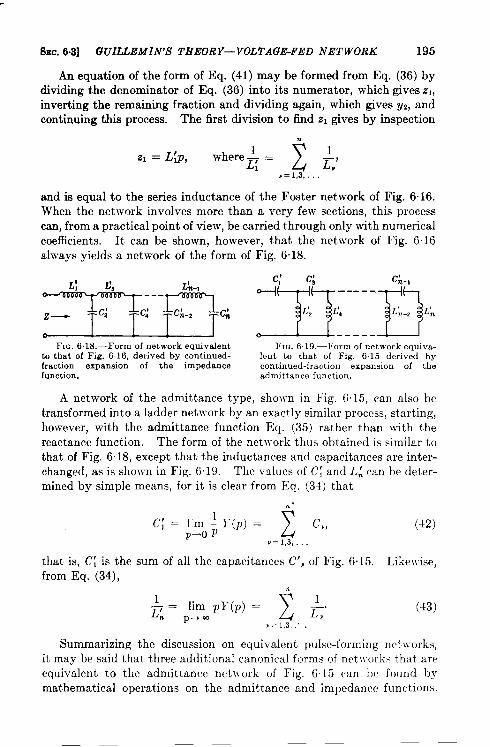
SEC. 6.3] QUILLEMIN’S THEORY—VOLTAGE-FED NET WORK 195
An equation of the form of Eq. (41) may be formed from Eq. (36) bydividing the denominator of Eq. (36) into its numerator, which gives zI,inverting the remaining fraction and dividing again, which gives v2, andcontinuing this process. The first division to find zl gives by inspection
n
where ~ =z
1Z1 = Lb,L; r,’
“=1 ,3,...
and is equal to the series inductance of the Foster network of Fig. 6.16.When the network involves more than a very few sections, this processcan, from a practical point of view, be carried through only with numericalcoefficients. It can be shown, however, that the network of Fig. 616always yields a network of the form of Fig. 6.18.
L: L!,
~o= TLn-’Tc’ %<:~”
.---fiz— c; : =;
FIG,6.18.—Form of network equivalent FIG. 6.19.—Form of network equiva-to that of Fig. 6.16, derived by continued- lent to that of Fig, 615 derived byfraction expansion of the impedance continued-fraction expansionfunction.
of theadmittance function.
A network of the admittance type, shown in Fig. 615, can also betransformed into a ladder network by an exactly similar process, starting,however, with the admittance function Eq. (35) rather than with thereactance function. The form of the network thus obtained is similar tothat of Fig. 6.18, except that the inductances and capacitances are inter-changed, as is shown in Fig. 6.19. The values of C; and L: can be deter-mined by simple means, for it is clear from Eq. (34) that
n“
c: = ho: }“(p) = 2 c,,
.= 1,3,...
(42)
that is, C; is the sum of all the capacitances C’, of Fig. 6.15. Likewise,from Eq. (34),
n1
P. z= lim pY(p) = # (+3)
p-) m ““=1 ,3,,, .
Summarizing the discussion on equivalent pulse-forming networks,it may be said that three additional canonical forms of networks that areequivalent to the admittance network of Fig. 615 can be found bymathematical operations on the admittance and impedance functions.

196 THE PULSE-FORMING NET WORK [SEC. 63
Many more equivalent networks can be found by combining thesemathematical operations in various ways, but most of these additionalnetworks are of only limited interest. The form or forms of networks tobe used in practice are determined by such practical considerations asease of manufacture and specific pulser requirements.
Networks of Equal Capacitance per Section.—The most importantpulse-forming network obtained by combining the canonical network
forms is the type shown in Fig. 6.20,
%:~---$1
which has equal capacitances. Fromthe standpoint of mass productionin manufacture, it is highly desira-
a-----ficble to have all capacitances of equalvalue. This is particularly true for
FIG.6.20.—Pulse-fmmingnetworkhaving high-voltage networks because theequalcapacitances.condensers for these constitute bv
far the most difficult and expensive item to manufacture. The ne~-work of Fig. 6.18 has capacitance values that are not very far from equal,and is therefore chosen as the starting point in deriving the network ofFig. 6.20. The network derived under the condition that the capaci-tances be equal may be expected to have inductances in the shunt legsto compensate for the altered values of the capacitances. If the actualcapacitance in a given shunt leg is increased in transforming from thenet work of Fig. 6.18 to that of Fig. 6.20, the compensating inductancemay be expected to be negative, and vice versa. The detailed procedurefor the derivation of the equal-capacitance network is described below.
The capacitances of Fig. 620 are all known, each being equal toC~/n where C~ is the total energy-storage capacitance, whereas theinductances are all unknown. The admittance and impedance functionsfor the network are the known functions specified by Eqs. (35) and (36).In the unknown network of Fig. 6.20 it is noted that, if an impedanceL ,p is subtracted from the impedance function Z(p) so that
21(P) = -z(p) – LIP, (44)
a zero of Z1(p) appears—that is, the series combination of LIZ and Ccorresponds to a zero of Z1(p) or to a pole of Yl(p) = l/Z,(p). The
Cpadmittance of the series combination of L,2 and C is L,2CP2 + 1“ ‘ence~
the poles of Yl(p) corresponding to the Llz and C resonant section mustbe given by
r
d
1p=+ — = +pl,–L,2C
and Yl(p) can be expressed in the form

SEC. 6.3] GUILLEMIN’S THEORY—VOLTAGE-FED NETWORK 197
Y,(p) = ~ + * + Y,(p), (45)
where Yz(p) is a remainder admittance function regular at + pl.
The constants al and az can be found by algebra, for
al = lim (p –[
p–pi
P+P1P1)Y’(P) = P!+’l+’, z(p) – L,p 11 1.
$ [Z(P) – LPI.-,,= Z’(p,) – Ll”
Likewise,1
a’ = z/(–p,)–L,”
8ince Z’(p) is a function of p’, as may be seen by differentiating Eq. (37),al=as=a. Thus Yl(p) can be expressed as
Y,(p) = @---2:PP; + Y,(p). (46)
The first term of the right-hand member of Eq. (46) must be the admit-tance of LH and C in series, so
1Cp ~“P _ 2ap
L,,cp’ + 1 = 1 p’ – p;”
‘2 + L,*C
(47)
The identity (47) gives the following two equations for determiningthe two unknowns pl and LIZ:
1 Z’(p,) –Ll
“’=%= 2 ‘(48a)
and1
— = –p:,L12C
(48b)
where pf is a root of Z(p) — Llp = O; thus, L1 = Z(pl)/pl. From Eq.(36) it is evident that the roots of Z(p) – L,p = O are all of the formp:, and that there are n such roots. The root p: is found by eliminatingL,, between Eqs. (48a) and (48b), and is given by
1
[
Z(p,)
1–P? z~(p,) – ~ “~=T (49)
Since the value of C is known and only p, is unknown, Eq. (49) deter-mines pl.

198 THE P[’L.’SE-FORMI,VG .VETWORK [SEC.63
Then~ = Z(p,)
1—p, ‘1
L,, = —– cp~
= ; [Z’(p,)–L,].
(50a)
(50b)
It is clear that L 12 is negative for all cases for ~vhich p? is positive, andvice versa. In order to examine further the sign of the root p;, supposethat Z,(p) is expressed as the ratio of two polynomials—which is alwayspossible—that is,
N(P’)21(P) = ~“
The coefficient of the leading term of N(p2) then contains the factor(L; – L,), \rhere L{ is the first inductance in the network of Fig. 618.All the other factors for all the coefficients of the polynomial N(p’) arepositive because they are comprised of combinations of the inductancesand capacitances of the network. By Descartes’ rule of signs, N(p’) = O
can have no positive roots unless the coefficients of its terms have atleast one change of sign \vhen considered as a sequence. This change ofsign can occur only if (I.; — L J < 0, that is, if Ll > L;, in which casethere is a single positive root. Hence, if p; >0, it follows that L, > L;,
for \\-hichcondition LIZ is negative.The nature of the root p; may also be seen by expressing Eq. (49) in
a somewhat different form. For this purpose it is noted that
[1Z’(p) -w=p$ ~.
P P
If the form of Z(p) given by Eq. (37) is used,
2n–2z(p) A,—’y+
z
A,
B,p2 + 1+ AZ.
PP“.=2,’4, . .
and2.–2
[-1
–2.4, _ ~d Z(P) . _PI ~
z
A ,B,P:
P p=,, P; (B.p: + 1)2”“=2,4, . . .
Using this result, Eq. (49) becomes
2.–2
1
z
A ,B,p;–’ A,+ ——c (B”p; + l)”
.= 2,4,..
(51)

SEC. 6.3] GUILLEMIN’S THEOR Y—VOLTAGE-FED
or, as AO = l/CN and l/C = n/CN,2“–2
n—1
z
A,B.P;
7= (Bpp; + l)’”VZ-2,4
NET WORK 199
(52)
The range of variation possible for C maybe found by letting p: varybetween zero and infinity. The limits are
1n
= A. = $N, when p; = O,
271-21
2
A,
c+Ao+ ~+*+*+”””+~)
‘=CNB, Czn-z
The C~s are for the network of Fig. 6.16. Inasmuch as the series induct-ance Lzn of the network of Fig. 6.16 is equal to L{ of Fig. 6.18, it is clearthat the first capacitance C; of the latter network must be given by
Thus C must satisfy the inequalities
u;<+c. 2
orC;< C<CN. (53)
In particular, it is noted that
C; <c=:
is a condition to be satisfied if p? is to be a positive root of iV(p2) = O.
The foregoing procedure serves to determine Llz and Ll, and reducesthe degree of Zl(p) by 2. The whole process may then be repeated onthe remainder function Z’(p) = l/Yz(p), where Y,(p) is deiined by Eq.(46), and L2 and LM are thereby -LIZ LZJ n-l,ndetermined. A new remainder --
function z,(p) = 1/Y*(p) is left, L,-L,2L: L,;L2~---Lm LjiLn.l,,L
and the whole process can be re-peated again and again until allof the roots are exhausted. a----u
Since negative inductance canFm. 6.21.—Equal-capacitance mutual.
inductance network equivalent to that ofbe realized physically by the use of Fig. 6.20.
mutual inductance, the network of Fig. 6.20, in which the inductances
LIZ, &, . . . L(m-l)m are negative, may be realized by a mutual-induct-ance network of the form shown in Fig. 6.21. The latter network, how-

200 TIIE PULSE-FORMING NET WORK [SEC. 63
ever, is a very practical form because all the inductances, including themutual inductances, may be provided by winding coils on a single tubularform, and the condensers may then be tapped in at the proper points.
Design Parameters jor Guillemin Networks.—As has been seen, thereare only a few canonical types of network that simulate rectangularwaves. In contrast, Guillemin’s networks have a pulse-shape parameter(a in the formulas) which is, in effect, the fractional rise and fall time ofthe generated pulse. This parameter may be chosen arbitrarily to haveany value between zero and one-half. The value zero corresponds tothe rectangular pulse and the value one-half corresponds to a triangularpulse. The number of network sections required to simulate the pulseshape corresponding to any given value of a is more or less in inverseproportion to a, that is, a one-section network is satisfactory for a = ~,whereas a very large number of network sections are required to give arectangular pulse shape, corresponding to a small value of a.
In addition to the parameter a, there is another factor in Guilleminnet works which may be varied, namely, the shape of the rising and fallingsections of the pulse. The treatment herein has been limited to pulseshapes having linear and parabolic rising and falling sections. A greatmany more types are possible, but it does not appear profitable to con-sider them here, l’ulse shapes having rapid rates of rise can be satis-factorily generated by networks that simulate trapezoidal pulses havingsmall values of a; pulse shapes having slower rates of rise are satisfac-torily produced by networks that simulate parabolic-rise pulses havingsomewhat larger values of a.
The first Guillemin networks were designed on the basis of a trape-zoidal pulse shape having a rise time of approximately 8 per cent. Bothfive- and seven-section networks were built, but the improvement ofthe seven-section over the five-section network was very slight. NOmore than five sections are therefore necessary to generate a pulse havingan 8 per cent rise-time parameter. Elimination of the fifth section wasfound to have an appreciable, although small, deteriorating effect onthe pulse.
The number of network sections necessary to give good pulse shapecan be estimated with fair accuracy by observing the relative magnitudesof the Fourier-series coefficients for the corresponding steady-statealternating-current wave. In the case of the five-section network justdiscussed, the relative amplitude of the fifth to the first Fourier coefficientis 0.04 and that of the sixth to the first is 0.02. In this case, the elimina-tion of all harmonic components having amplitudes relative to the funda-mental of 2 per cent or less has an inappreciable effect on the pulse shape,whereas the effect of eliminating the 4 per cent harmonic is appreciablealthough still smal!.
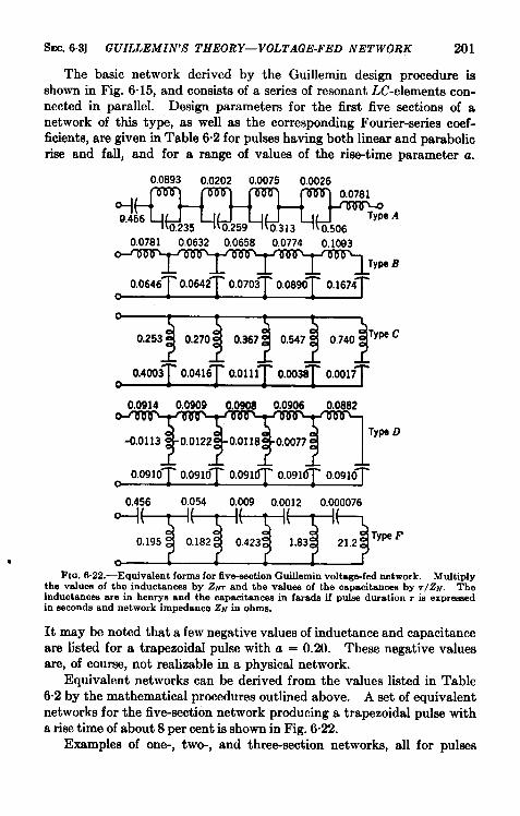
SEC. 6.3] GUILLEMIN’S THEORY—VOLTAGE-FED NETWORK 201
The basic network derived by the Guillemin design procedure isshown in Fig. 6.15, and consists of a series of resonant LC-elements con-nected in parallel. Design parameters for the first five sections of anetwork of this type, as well as the corresponding Fourier-series coef-ficients, are given in Table 6“2 for pulses having both linear and parabolicrise and fall, and for a range of values of the rise-time parameter a.
0.0893 0.0202 0.0075 0.0026
0-l9.466
0.0781 0.0632 0,0658 0.0774 0. loe3
~ TypeB
0.0646 0.0642 0.0703 0,0890 0.16740
0.253j0.270~ 0.36j0.547j 0.740~c
o
A -L -L J- -L
0
0.456 0.054 0.009 0.0012 0.000076
O-I(
0.195
0FIG.6.22.—Equivalent forms for fivwjection Guillemin voltagefed network. Multiply
the values of the inductances by ZNTand the valuesof the capacitance by r/ZN. Theinductancesare in henrysand the capacitancesin faradsif pulseduration* is expressedin secondsandnetworkimpedanceZNin ohms.
It may be noted that a few negative values of inductance and capacitanceare listed for a trapezoidal pulse with a = 0.20. These negative valuesare, of course, not realizable in a physical network.
Equivalent networks can be derived from the values liskd in Table6.2 by the mathematical procedures outlined above. A set of equivalentnetworks for the five-section network producing a trapezoidal pulse witha rise time of about 8 per cent is shown in Fig. 6.22.
Examples of one-, two-, and three-section networks, all for pulses

!5’N1
TABLE 6.2.—VALUESOFINDUCTANCESANDCAPACITANCESFORFIVE-SECTIONPULSE-FORMINGNETWORKOFFIG. 6.15II I I
II Fourier coefficients
waveform . !, I
II b, b,I
bsI
b,
Rectangular o 1.2732 0.42440.2547 0.1s19Trnpezoidd 0.05 1.2679 0. 40s9 0.2293 0.1474Trapezoidal 0.08 1.2601 0.3854 0.1927 0.1015Trapezoidal 0.10 1.2524 0.3643 0.1621 0,0669Trapezoidal 0.20 1.1911 0.2141 0 – 0.0393Parabolic rise 0.05 1.2699 0 4166 0.241S 0.1640Parabolic rise 0.10 1 2627 0.3939 0.2064 0,1194Parabolic rise 0.20 1.2319 0,3127 0.1032 0.0246Parabolic rise 0.25 1.2092 0.2610 0.0564 0.0035:Parabolic rise o 33 1 1609 0 1720 0. 00?330 0.00331Parabolic rwe 0,40 1,1142 0, 10s0 o 0, 00s5Parabolic rise 0,50 1.0319 0,03S2 0. 00S25 0. 0030(
I Inductance I Capacitance
bs L, L, Lb L, L* c, c, c, c, c?, zh
. — - — — — .
0.1415 0,2500 0.2500 0.2500 0.250Q 0.2500 0 4053 0.04503 0.01621 0. 06S27 0,00500:
0.0988 0.2510 0,2595 0.2777 0.357s 0.357s 0.4036 0.0431s 0.01459 0.00670 0.00349 ~0, 04S2 0.2526 0.2753 0.3303 0,447s 0.7340 0.4011 0.04089 0.01227 0.00462 0.00170 >0.0155 0 2542 0.2912 0.3927 0.6796 2.2S75 0. 39s7 O.03S65 0.01032 0.00304
–0.0147 O 2672 0.4455 - –1.1561 – 2.4052 0.3791 0.02272 0 0.00179 -0.1194 0,2507 0.2547 0.2632 0.2773 0.2961 0.4042 0.04420 0,01539 0.007450.0691 0,2521 0.2694 0. 30s4 0. 380s 0,5122 0 4019 0.04179 0.01314 0.005430.0017 0 25S4 0.3393 0.616s 1. S472 20.94 0 3921 0.0331s 0.00657 0,001120.0017 0 2632 0.4065 1.1292 12. SS7 21.37 0 3s49 0.02769 0.00359 0.000160.0064 0,2742 0.616s 6. S493 13,44 5.5556 0,3695 0.01S25 0.00059 0.000150,0015 0 2857 0.9821 m 5.346 23.15 0 3547 0.01146 0 0.000390.0014 0 30s5 2 7747 7 7160 15.15 25.00 0.32S5 0,00406 0.00053 0.00014
I I I I I I Ill
0,00055-0.000520.004220.002440.000060.000060.000230.000050.00005 j
Multiply the inducta”cea by ZW and the capacitance~by r/ZN. The inductances are given in henrys and the capacitance in farads if the p“bje d“raticm sin expreeaed in seconds and the network impedance ia in ohms. a i8 fracticmalri.e time of wave, me Figs 6-13aandb.
.v.
i(t) = fi I b. sin $.
“=1,3, . .
.
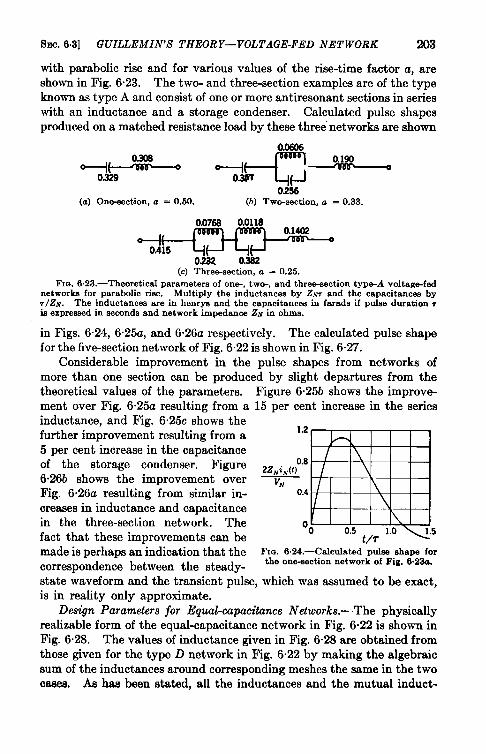
SEC. 6.3] WJILLEMIN’S THEOR Y—VOLTAGE-FED NETWORK 203
with parabolic rise and for various values of the rise-time factor a, areshown in Fig. 6.23. The two- and three-section examples are of the typeknown as type A and consist of one or more antiresonant sections in serieswith an inductance and a storage condenser. Calculated pulse shapesproduced on a matched resistance load by these three networks are shown
ao606
e--&* --I-I0.190
(——J———0256
(a) One-cection, a = 0.S0. (b) Two-section,a = 0.33.
0.0766 0.0118
0.41502a2 0.382
(c) Three-section, a = 0.25.FIG. 6.23.—Theoreticcl parameters of one, twc-, and three-cection type-A voltage-fed
networks for parabolic rise. Multiply the inductances by ZNT and the capacitances byr/ZN. The inductances are in henrys and the capacitances in farads if pulce duration ric exprecced in seconde and network impedance ZN in ohnm
in Figs. 6.24, 6.25a, and 6.26a respectively. The calculated pulse shapefor the five-section network of Fig. 6.22 is shown in Fig. 6.27.
Considerable improvement in the pulse shapes from networks ofmore than one section can be produced by slight departures from thetheoretical values of the parameters. Figure 6“25b shows the improve-ment over Fig. 6.25a resulting from a 15 per cent increase in the seriesinductance, and Fig. 6.25c shows thefurther improvement resulting from a
12
5 per cent increase in the capacitanceof the storage condenser. Figure *Z~i~[~~86026b shows the improvement over VMFig. 6.26a resulting from similar in- 0.4
creases in inductance and capacitancein the three-section network. The ofact that these improvements can be
5
made is perhaps an indication that the Fm. 6.24.—Calculatedpulse shape for
correspondence between the steady- theone-sectionnetworkof Fig. 6.23a.
state waveform and the transient pulse, which was assumed to be exact,is in reality only approximate.
Design Parameters for Equal-capacitance Networks.—The physicallyrealizable form of the equal-capacitance network in Fig. 6.22 is shown inFig. 6.28. The values of inductance given in Fig. 6.28 are obtained fromthose given for the type D network in Fig. 6.22 by making the algebraicsum of the inductances around corresponding meshes the same in the twocases. As has been stated, all the inductances and the mutual induct-

204 THE PULSE-FORMING NETWORK [SEC. 6.3
1.2
w:
o
t/75
(a) Theoretical parameters.
1.2
0.8
2ZNi“ (t)
—0.4f m‘N
oo~.,t/7
v“ 0“4tH—tH—h2ZN i“(t)
‘- -
Otzrtmuo 0.5 1.0 1.5
t/7(c) l,, increased 16 per cent, CN in~rea~ed
5 per cent from theoretical value.
~ P+’Nd RI- ZN
a- ~. Parablic rise.
(b) L4 increased 16 per oent from thea-retioalvslue.
klu. 6.25.—Caloulated pulse shapes for the two-section network of Fig. 6.23b.
1.2 1.2
m
70.8 0.8 7
2ZN ;N(t) 2ZM i~(t)VN 04 v’ 04
0 0.5 0 0.5 1.0 1.5
t/7(a) Theoreticrdparameters. (b) L4increased 21 per cent, (’,, imvwwc[i -t
per cent from theore tic,,] vwl”e.
46
‘“m’=’
a= ~ parabolic riseFlu. &26.-Caiculated pulse shapes for the tilree-sect io,) nrt work of Fig. &WC

SEC. 6.3] GUILLEM IN’S THEORY—VOLTAGE-FED NET WORK 205
antes may be obtained by winding coils on a single tubular form, and byndj ust,ing the spacing between successive coils; however, care must betaken to insure that mutual-inductance effects between alternate coilsare negligible.
The networks derived from the 1
theoretical type D network by re-placing the negative inductances
2zNiN(t)0in series with each condenser by —
VNmutual inductances between ad- 0jacent coils are normally referredto as type E networks. Experi-mental work done in early 1942 5by J. R. Perkins proved the valid- t/7ity of the assumptions made in FIG. 6.27.—Calculatedpulse shape for the
designing networks with induct-five-secticmnetworkof Fig. 6.22.
antes as given in Fig. 6.28. Further simplifications can be made, how-ever, by noting that the values of the inductances of the three centersections and of the mutual inductances from section to section are verynearly equal. It has been found in practice that they can be made equalwithout affecting the pulse shape appreciably.
One way of reducing a type E network to thk latter physical form
A
04801
Fm. 6.28.—Equal-capacitance mutual-inductance network equivalent to the equal-capacitance network in Fig. 622. Theinductancesare in henrys and the capaci-tances in farads if the pulse duration isexpressed in seconds and network impedancein ohms.
consists in winding a continuoussolenoid in such a way that itstotal inductance LN = rZ~/2.The total network capacitance,C~ = r/2Z~, is divided equallybetween the sections, and eachcondenser is connected to a tapon the solenoid. The taps arelocated to obtain equal inductancefor all sections except the ends,which should have 20 to 30 percent more self-inductance, and theratio of length to diameter of thecoil is chosen by a method involv-ing the use of Nagoaka’s functionto give a mutual inductance whichis 15 percent of the self-inductance
of each center section. The relative values of inductance and capacitanceobtained by this method show good agreement with those given in Fig.6.28, and networks of five or more sections built in this manner giveexcellent results. The same pulse shapes can be obtained, however, bythe use of coils judiciously designed and located, as long as the sum of

206 THE PULSE-FORMING NETWORK [SEC. 6.3
their self- and mutual inductances agrees closely with the values ofFig. 6.28.
If networks of less than five sections are to be designed, it is usuallyfound that it is no longer possible to obtain satisfactory pulse shapes byusing the same inductance per section. If the values corresponding to atype D network are knonm, the necessary values of self- and mutualinductances can again be computed, and the coils wound and spaced theright distance to duplicate these values. Or, charts can be obtainedexperimentally to determine the percentage inductance for each sectionand the total mutual inductance required to give a pulse shape that hascertain characteristics of time of rise and ripple. The number of sectionsin the network varies with the time of rise required for the particularapplication: practical experience indicates that it is not always desirableto obtain a very fast rise (see, for instance, discussion on magnetron mode-changing in Chap. 10 of this volume and in Chap. 8 of Vol. 6); and, ingeneral, a shorter time of rise results in a ripple of higher amplitude onthe top of the pulse. Practical considerations involving the size of thecondensers and the inductances, as well as the effect of other pulser com-ponents, make it generally undesirable to use a large number of sectionsfor very short pulses. Experience gained with type E networks showsthat optimum over-all results are usually obtained for the followingnumber of sections: 1 to 3 for pulse durations of less than 0.5 psec, 2 to 5for pulse durations from 0.5 to 2.5 ~sec, and 3 to 8 for pulse durationsfrom 2.5 to 5.0 psec.
To recapitulate, the Guillemin theory provides a means of designingpulse-forming networks that duplicate accurately the pulse shapes nor-mally required on a resistance load. It is then possible to compute theactual pulse shape produced by the theretical network and, by judiciouschanges in some of the parameters, to approximate even more closelythe desired pulse shape.
The theoretical design procedure is likely to be lengthy, especiallyfor networks of more than two sections. In practice, therefore, it wasfound easier to derive experimentally any variations from the Guillemindesign for a given pulse shape and number of sections, rather than towork through the detailed theory for each variation. The experimentalprocedure is necessary in any case to compensate for unavoidable sim-plifications in the theory. Stray capacitances and inductances, the effectof different qualities of dielectrics, the nonlinear and reactive character-istic of the load, and losses in the network cannot be accounted for easilyin any kind of theoretical computation.
For instance, the pulse photographs of Fig. 6.29 show the modifica-tions in pulse shape that can be obtained by altering some of the param-eters of the network of Fig. 6.30. The first photograph shows the

SEC. 6.4] CURRENT-FED NETWORKS 207
(a) Normal. (b) 20 per cent added ca- (c) 20 per cent added cdpacitance between pacita,lce betweenpoints 1 and4. points 3 and 4.
(d) 10percent added induc- (e) 10 per cent added in. (f) 10 per cent added ca-tance at point O. ductance at point 3. pacitance between
points 1 and5.
(p) 10 per cent added ca- (h) 10 per cent added ca- (f) 10 per cent added ca-pacitance between pacitance between pacitance betweenpointe2 and 5. points 3 and 5. points 1 and 5, 2 and 5,
and 3 and 5.FIG. 6.29.—Effect of variations in the values of L and C on the pulse shape obtained
with a type E network. The numbered circuit points correspond to those shown inFig. 6,30.
Iesired pulse shape after the parameters of the network had been adjustedexperimentally. The next four indicate the effect of changing the valueof some of the parameters, and thelast four show the effect of stray ca-
Pulse-formingnetwerk~._. ——_7
pacitance from various points of the ,r I
~oil to ground. The ~hanges in
L1,U 1
ipulse shape obtained for small vari- ‘---ations in parameters indicate theease with which it is possible to meetspecific requirements, but the~ also 10 40 ,show the necessity of holding the 5 ,.
11123
u! .,values of elements to close toler- ~ ,o,y~chrmco:---------antes and of minimizing the straycapacitances. FIG.6.30.—CircuitdiagramforFig.6.29.
6.4. Current-fed Networks. -Current-fed networks are distinguishedfrom voltage-fed networks in that the energy is stored in inductances

208 THE PULSE-FORMING NET WORK [SEC. 6.4
instead of in capacitances. A current-fed network is therefore rechargedby building up a current in an inductance that is an integral part of thenetwork. Upon discharge, a portion of the built-up current appears inthe load in the form of a puke whose shape may be controlled by varyingthe network construction. The whole theory of current-fed networks isentirely analogous to that of voltage-fed networks, except that the cur-rent rather than the voltage plays the primary role.
As in the case of voltage-fed networks, it is instructive to considerfirst those current-fed networks that produce ideal rectangular voltagepulses on resistance load. The voltage across the resistance load for anideal rectangular pulse is defined by the function o(t),
(VI, for O<t
v(t) =
o, for t > T.
The corresponding Laplace transform, v(p), is
<7,
v(p) = ~ (1 – e–~). (54)
In solving this problem, it is simpler to consider the inverse case-that is.
m1/?Current-fed G,nelwork of
s dmittance Y vt~)
FIG. 6.31 .—Schematic circuit forgenerating a rectangular voltage pulseby charging a current-fed network anda load of conductance GJ in parallel.
the case for which the puke is pro-duced by charging the network in par-allel with the load resistance from aconstant-current source. Since thepulse produced by discharging thenetwork is identical with the chargingpulse, the two cases are equivalent asfar as determining the form of thenetwork is concerned.
The charging pulse is generatedby opening the switch S in the circuit
shown in Fig. 6.31. The Laplace-transform equation for the circuitwritten on a current-node basis is
(YN + G,) u(p) = $ (55)
where Y~ is the network admittance, GJis the load conductance, and IN
is the initial current from a constant curfent source. Solving for YN,
INYN=— –Gl=
IN– G1
W(P) VI(1 – e-~)
(56)

Sac. 6.4] CURRENT-FED NETWORKS 209
If the numerator and denominator aremultiplied bye~i2and the termsrearranged to introduce the coth function, there results
‘~=’fcothf+(!!c)l ’57)
The constant IN has been treated as known, but is in fact arbitrary.Choosing
1~ = 2G1V2,
the expression for YN reduces to
Y. = ‘1 coth $. (58)
By substituting Eq. (58) in Eq. (55) and solving for v(p), the unknownquantity, it may be seen that ZN = 2G1V1 is the correct choice for IN.
The expression G1coth pr/2 is recognized as the input admittance of alossless transmission line of characteristic impedance Zo = I/Gl and ofelectrical length r/2 when the far end of the line is short-circuited. Therequired current-fed network must, therefore, be either a transmissionline of this type, or an electrical equivalent of such a line.
The functioning of the short-circuited transmission line in producingthe desired rectangular pulse nMy readily be understood in terms of theelementary theory of wave propagation on such a line. At the instantat which the switch is opened, the current 10 from the constant-currentsource divides equally between the line and the resistance load if theresistances of the two are equal. A rectangular voltage wave of ampli-tude ~lOZOtravels down the line, is totally reflected with reversal of signat the short-circuited end, and travels back to the input end in a totalelapsed time of 28 = r. When the reflected wave reaches the input end,the voltage there drops immediately to zero and remains zero thereafterbecause the line is properly matched by the resistance RI = 20, and thereis no reflection at the input end. However, the line is fully charged withmagnetic energy because a constant current of value 10 is flowing throughit. The voltage pulse generated at the load during the charging periodclearly has an amplitude of 410Rl and duration 26.
If the circuit between the constant-current source and the transmis-sion line is then broken, an exactly similar voltage pulse is generated bythe resulting discharge of the magnetic energy stored on the line. Thetotal energy stored on the line is ~Ld& where LO is the total distributedinductance of the line. This ener~ must be equal to that dissipated inthe load, or

210 THE PULSE-FORMING NETWORK [SEC. 6.4
which reduces to the relation
(59)
The analogy between the transmission ‘line used as a voltage-fed cur-rent-pulse-generating source and as a current-fed voltage-pulse-generat-ing source is very close. The far end of the line is open-circuited whenit is used as a voltage-fed network and short-circuited when it is usedas a current-fed network. In the first case, the line is charged to a volt-age Vo, which produces a current pulse on matched load of amplitudeVO/2RI; in the second case, the I’ne is charged to a current 10, whichproduces a voltage pulse on matched load of amplitude
IO I@.
fml= 2
Current-fed Networks Derived from a Transmission Line.—Current-fednetworks may be derived from the short-circuited transrnission line bymethods exactly analogous to those used in Sec. 6.3 in deriving voltage-fed networks from the open-circuited transmission line. A summary ofthe networks thus derived is included, but the details of the derivationsare omitted as they are considered sufficient y obvious.
Current-fed Network Simulating a Uniform Line Derived by Rayleigh ’s
Principb.-This network, shown in Fig. 6.32, is identical in form to thevoltag~fed network of Fig. 6.15 except that the far end is shorbcircuitedinstead of open-circuited.
21!TI!Im---clFIG. 6.32.—Current-fed pub-forming net- Fm. 6.33.—Current-fad network de-
work of the uniform-line type. rived by rational-fraction expansion of theWmmniAon-line admittance function.
Current-fed Networks Derived by Rational- fradion Expansions of the
Admittame and Impedance Functions of a Short-circuited Transmission-line. -These are analogous to the similar networks derived by rational-fraction expansions of the impedance and admittance functions for theopen-circuited transmission line. The network derived by expanding theadmittance function
Y = Yo coth ~
is shown in Fig. 6.33.

SEC.6.4] CURRENT-FED NETWORKS 211
Similarly, the network derived by the rational-fraction expansion ofthe impedance function
Z = Z, tanh $
is illustrated by Fig. 6.34.Curreti-fcd Networks of the Guillemin Type. —l’he theory of the
Guillemin current-fed network is similar to that of the voltage-fed net-work, except that the roles of the voltage and current are interchanged.Instead of generating a specified steady-state alternating current byapplying a constant-voltage source to the unknown voltage-fed network,
:~-:~ mFto. 6.34.—Current-fed network de- Fm. 6.35.—Circuit for generating a spec-
rived by rational-fraction expansion of the ified alternating-voltage wave similar to thetransmission-line impedance function. desired singbprdw shape.
a specified steady-state alternating voltage is generated by applying aconstant-current source to the unknown current-fed network. Comparethe circuit of Fig. 6.12 with that of Fig. 6.35. The alternating-voltagewave in this case is started by opening the switch rather than by closingit as in the case of the voltage-fed network.
A Fourier-series expansion is made for the specified alternating-voltage wave 6hape and the coefficients of the resulting series are identifiedwith the network of Fig. 6.36.
The voltage across the vth anti-
~ a----o
resonant section is given by
J
L, .v, = Ih.
c ‘ln , , (60)FIG. 6.36.—Form of current-fed net-
A comparison of Eq. (60) with Eq.work derived by Fourier-series analysis ofa specified alternating-voltage waveform.
(33), which is the correspondingexpression for the voltage-fed network, shows that the two are identicalin form with the exception that IN appears in Eq. (60) instead of V~ andthat L, and C, are interchanged. AH of the results derived for the volt-age-fed network may be immediately applied to the current-fed networkby making the changes stated in the previous sentence.
In particular, the values of L, and C, are given by the equations
(61)

212 THE PULSE-FORMING NET WORK
and
(62)
The parameter values given in Tables 6.1 and 6.2 for the voltage-fednetwork of Fig. 6.15 apply direct] y to the current-fed network of Fig.6.36, provided that the L,’s and C,’s are interchanged and the induct-
-J’0.0646 0.0642 0.0703 0 0.164
Type0.0781 0.0632 0.0658 0.0774 0.1G93 B
o0.0416 0.0111 0.00378 0.00169
w , . } 1H) ,. t (uI ,~0.253 0.270 0.367 0.547 0.740 TyCw
1{ l\ II Ii l\0.195 0.~~2 0.423 1.83 {).2
l\ l\ 1(
0.0012 0.000076 TypeF
(TypeD not physicallyrealizable)FIG. 6.37.—Equivalent forms for five-section Guillemin current-fed networke. Multi-
ply the inductances by Zwr and the capacitances by r/Z,V. Inductances are given in henrysand capacitances in farads if the pulse duration r is in seconds and the network im@=”ceZN is in ohms.
(4) One-section, a = 0.50. (b) Two-section, a = 0.33.
(c) Three-section, a = 0.25.FIG. 6.3S.—On&, twe-, and three-section type A current-fed networks. Multiply the
inductances by ZNT and the capacitances by r/Z~. Inductances are given in henrys andcapacitances in farads if the pulse duration r is in seconds and the network impedanceZN is in ohms.

SEC. 6.5] MATERIALS AND CONSTRUCTION 213
antes are written in terms of r/ YN = Zm and the capacitances in termsof Ym = ,/2”. As an example, reference to Table 6.1 row 1 gives thefollowing values for the corresponding current-fed network
Likewise the voltage-fed networks shown in Figs. 6.22 and 6.23 canbe transformed to current-fed networks by following an identical pro-cedure. The current-fed networks thus derived are showm in Figs.6.37 and 6.38. The five-section networks are correspondingly designatedin Figs. 6.22 and 6.37. The type D current-fed network is not realizablein physical form because some of the capacitances are negative. It is
“therefore omitted from Fig. 6.37.6.6. Materials and Constructional Cm”k.—The losses in the coils of
a network can be determined by calorimetric measurement during opera-tion, provided that the coils can be thermally insulated from the con-denser elements. An alternate method is to calculate the frequency
Fm. 6.39.—Condenser-discharge currents in the four-eection type-,?l network fFig. 6.40.
]hown in
distribution of the currents in the various coils, and to determine the Qof the coils at those frequencies either by calculation or by measurement.The Q of a coil may often be calculated approximately with the use ofone of various empirical formulas which are given in handbooks. Itis usually much easier, however, to measure the Q of a sample on an r-fbridge, The frequency distributions may be calculated from Table 6.2.
The calculation of losses in the coils and in the condensers of a typeE network during discharge may be simplified by the usc of a singleeffective frequency instead of the band of frequencies given by Table6.2. The discharge currents in the condensers of a four-section type Enetwork are shown in the oscillogram of Fig. 6.39 as obtained with thecircuit of Fig. 6.40.
IBy P. R. Gillette.

214 THE PULSE-FORMING NETWORK [SEC. 6.5
The following approximate method of calculating this effective fre-quency leads to values of losses that are accurate enough for all practicalpurposes, although the frequency itself may be inaccurate. The actualcurrents shown in Fig. 6.39 may be represented approximately by por-
?ulse!ormmgnetworkR1.~N~–––––––_7
m!---.1.It, i2i3i41
L________. JFIG. 6.40.—Circuit diagram for
lJig. 6.39.
tions of sine waves as shown in Fig. 6.41a.The current in the end condenser is as-sumed to consist of two overlapping wavesof the same form as those for the othercondensers. These waves may be addedto give the coil currents, as indicated in Fig.6.41. The frequency of the sine waves,in terms of the number of sections and thepulse duration, is given approximately by “the expression f = n/2r. The effective
frequency for the rise and fall of current is given to a similar degree ofaccuracy—that is, to within a factor of two-by the same expression.
The discharge currents in the coils may each be broken up into arising, a fla,t, and a falling portion, and the losses calculated separatelyfor each portion. The power dissipated in a coil during the rise and fallmay be calculated on the assumptions(1) that the current is a sine wave ofperiod equal to four times the risetime and of peak amplitude equal tothe pulse amplitude, and (2) that theeffective resistance is the a-c resist-ance corresponding to the frequencyof this sine wave. The power dissi-pated during the flat portion of thepulse may be calculated on the as-sumption that the current is a directcurrent of magnitude equal to thepulse amplitude. The power dissi-pated during the charging period maybe calculated on the assumption thatthe current is a sine wave of frequencyequal to half the mdse recurrence fre-
(a) in the condensers,
Time —
(b) in the coils.Fm. 6.41 .—Simplified represents.
tions of currents in the elements of ,Spubs-forming network.
q;ency. The to~al average power dissipated in the coil is the sum of thevalues of losses computed as above.
In this way the correct wire size, the respective merits of solid,stranded, and litz wire, and coil shapes (single-layer, bank-wound, etc),may be determined. The power loss is usually a far more importantconsideration than is current density in the choice of wire size. Lossesin coil forms may be reduced by the use of materials having low dielectric

SEC. 6.5] MATERIALS AND CONSTRUCTION 215
loss and by the use of hollow rather than solid forms. Increasing the Qof coils by increasing their size may cause difficulties unless care is takento keep the self- and mutual inductances constant.
In addition to the generation of heat, the effect of losses in the coilsis prirnarily to attenuate the high frequencies. A pulse with a smoothertop and a slower rate of rise is thus produced with coils of higher losses.
Condemwrs.-A network that satisfies all electrical requirements canbe constmcted of separate coils and standard mica condensers of suitablecurrent and voltage ratings. A bulky network results, however, becauseof the problem of insulating the separate components, and also becausethe current ratings of standard condensers are based on continuousoperation rather than on duty ratios of about 0.1 per cent. The expe-dient of overrating smaller conventional condensers is,dangerous becausethey are designed with interdependent voltage and current ratings. Ithaa therefore been found necessary to develop new techniques in designand construction. All components are put in one container, with com-mon means of insulation. The condensers are designed to withstand thehigh voltages, but have a smaller current-carrying capacity than isordinarily associated with such voltages.
Losses in the condenser elements can be calculated and measured bymethods analogous to those suggested for coils. The losses may bemeasured calorimetrically, or the effective frequencies may be calculatedby one of the two methods outlined in the discussion of coil losses, and theeffective dissipation factor of the completed condenser either measuredor calculated for those frequencies. The effective dissipation factorincludes the losses in the dielectric, the foil, and the impregnant. Undermost conditions, the effective current through the condenser foils is wellwithin the current-carrying capacity of the thinnest commercial foils.For high duty ratios and short pulse durations, where the skin depth isless than the foil thickness, the foil resistance may become a limitation.
Dielectrics such as mica, oil-impregnated paper (hereafter referred toas “paper”), and a relatively new material known as diaplex have beenused successfully. Diaplex is m organic-inorganic material that wasdeveloped as a substitute for mica, and has been used in a number ofspecial applications for which the requirements are especially stringent.Paper, the material used most commonly in high-voltage condensms,has found by far the widest application in network manufacture. Micaand paper condenser elements are almost always oil-filled; diaplex unitsare usually oil-filled, but it is also possible to use a plastic material as abonding medium.
In general, best results are obtained when the losses in a network areevenly divided between the inductive and capacitive reactance. Ifthis rule is followed, it is generally possible to use paper dielectri$ for the

216 THE PULSE-FORMING NETWORK [SEC. 6.5
condensers. In this case, the temperature-limiting constituent of thecondensers is the paper dielectric, and that of the coils is the enamel orother organic insulation. If mica or diaplex dielectrics are used in thecondensers, and the coils are wound with glass-insulated wire, the phenolicinsulating members, impregnating oil, and solder become the tempera-ture-limiting Constituents. Mica or diaplex is therefore used as thedielectric in high-temperature units, and special high-temperature typesof phenolics, oils, and solders are employed in the construction of thenetworks.
A ‘‘ hot-spot “ temperature, the maximum stable operating tem-perature of the materials, is generally taken as a maximum both forCon&nsers and coils. In paper condensers, the amount (thickness) ofpaper dielectric is determined by the hot-spot temperature, which isusually 125eC. If the thickness of dielectric has been chosen with regardto this temperature, the occurrence of corona in the paper may easilybe avoided by conventional methods. The same consideration appliesto diaplex at low and medium voltages. However, corona will appear atthe higher voltages if a liquid impregnant is used, apparently becausestrong electric fields drive the oil out from between the layers of dielec-tric material.
For mica condensers, the losses increase at a much greater rate thanthe applied voltage, partly because of corona in the voids of the micaitself. Hence, measurements made when the input power is low are notadequate to determine the maximum power that can be applied withoutexceeding the safe temperature for the other components. Mica is uniqueamong dielectrics in that corona of moderate intensity does not producechemical degradation of the dielectric, which would induce further 10SWS.In this respect, paper is by far the womt of the three types of dielectricunder discussion. Dielectric losses may also increase faster than theapplied voltage with materials other than mica. Hence, empirical life-testing of the network is an important part of the design procedure.
Some of the electrical characteristics of mica, diaplex, and oil-impreg-nated paper condensers are listed in Table 6“3.
TABLE 6.3.—ELECTRICAL CHARACTERISTICS
Mica Diaplex Paper
l—l—————— l—Dielectricconstant (25°C, l kc/see) . . . . . . . . . . . . . . . . . . . . . . 6.7 4.8
I3.8
Dissipationfactor (25”C, lkc/see, %) . . . . . . . . . . . . . . . . . . . . 0.15 0.35 0.2
The variation with frequency and temperature of the capacitance anddissipation factor of condensers constructed with the three differenttypes of dielectric is illustrated by the curves in Figs. 6.42 and 643.

SEC. 6.5] MATERIALS AND CONSTRUCTION 217
Whereas the dielectric constant of mica and diaplex is nearly inde-pendent of frequency, that of paper decreases as the frequency is increased,particularly at low temperatures. Therefore, the energy stored in papercondensers of a pulse-forming network cannot be entirely removed inhigh frequency components of the pulse shape. Thus, at low tempera-
tures, short pulses of 0.5 wsec or less have a duration shorter than thatwhich is predicted from low-frequency measurements.
I I I I II I I I II 1.GEcondenser with oil-n—
L=Gilpapr_dieletric__
---- ❑ Bonded16apTexcondenser— ASprague mica condenser
-- ---- -------- ___ =
3 A. 0,.
.E:B.G
%00
500100 C/S& 1 kc/see 10 kc/see 100 kc/aec 1 Mc/!
Frequency
FIG. 6,42.—Variation of capacitance with frequency and temperature.
The dissipation factor of paper becomes very great at high frequencies,indicating that, as the time delay per section is decreased, the propor-tion of losses in a paper network increases rapidly. In a mica or diaplexnetwork this effect is not nearly so pronounced. The increase in dis-sipation with frequency also causes the pulse from a paper network tobe more rounded than that fmrfi a similar mica or diaplex network.The curve showing dissipation factor as a function of temperature leadsto the interesting conclusion, borne out in practice, that the losses in apaper network are a minimum at 75°C.
To summarize, both mica and diaplex may be used to advantage insmall light-weight high-temperature units. Paper, because of its lowermaximum operating temperature, gives, in general, a more bulky net-work. It may be used in the storage condensers of type A networks,but the antiresonant sections usually require higher Q’s than may beachieved with paper. Finally, the rapid decrease in dielectric constantat low temperatures discourages the use of paper in units required tooperate at extremely low temperatures. Since paper is the least expen-sive of the three dielectrics discussed, it is generally chosen for applica-tions in which only a normal range of ambient temperature is encountered.
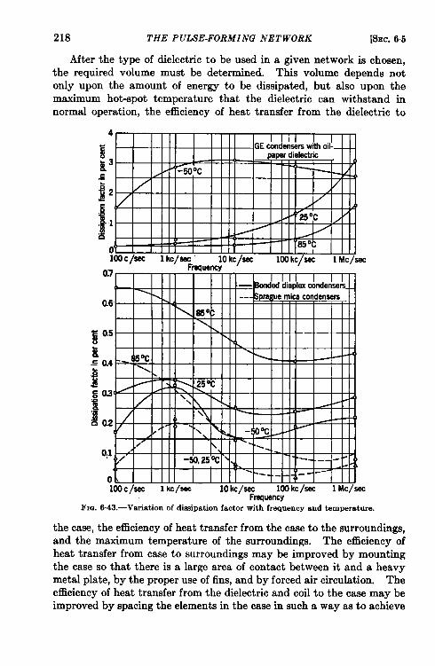
218 THE PULSE-FORMING NETWORK [SEC. 6.5
After the type of dielectric to be used in a given network is chosen,the required volume must be determined. This volume depends notonly upon the amount of energy to be dissipated, but also upon themaximum hot-spot temperature that the dielectric can withstand innormal operation, the efficiency of heat transfer from the dielectric to
liiiiiiiiiii ETf.. -
I III
ho C/s&1
1 kq$ec 10 kc/eec 100 kc/seeFrequency
1 Mc\sec
07
0.6
. \ , , , , , I I , , , I\
\
‘ Frequency “Fm. 6.43.—Variation of dissipation factor with frequency and temperature.
the case, the efficiency of heat transfer from the case to the surroundings,and the maximum temperature of the surroundings. The efficiency ofheat transfer from case to surroundings may be improved by mountingthe case so that there is a large area of contact between it and a heavymetal plate, by the proper use of fins, and by forced air circulation. Theefficiency of heat transfer from the dielectric and coil to the case may beimproved by spacing the elements in the case in such a way as to achieve

SEC. 6.5] MATERIALS AND CONSTRUCTION 219
the freest possible convection of oil, and hence the maximum convectivecooling action. Improvement in any of these factors reduces the requiredvolume of the dielectric.
I?IG. 644.—Typical ty&E networks.
Ezamples.—The four network designs listed in Table 6.4 are typicalexamples of networks used in pulsers for radar systems. The networksare shown in Fig. 6.44, and the pulse shapes produced on the appropriate.-resistance loads are shown in Fig. 6.45. - -
TABLE 6.4.—TYPICAL TYPE E NETWORKS
PeakPufse
Nom- Dimenaionn*charg- dura- PRF,
lmpe- inal No. ofNo. illg
tion, pmdance, pulse 8ec-
vOlt- ohrm power, tiona 1w., ., ht.,age,kv
*ec kw in. in. in.
— . — . — — — — . —
1 3.5 0.84 S40 50 25 32.24 420 3+5 li 3! 2i
. — . — . — — . — —2 8 0.25 1600 50 200 2 2 lot 5i
0.50 Soo 22.60 460 45.20 200 4+4
— — — — — — — — — —3 8 1.0 1000 50 200 5 3i 4* 5*
— — — — — — — — — —4 17 2,0 300 25 2000 2 4* 13* 94
wt.
12 Oz
5 lb9 on
4 lb906
24 lb11 Oa
Appli-Mfg.cation
Airborne GE
— —Airborne Sprague
Ground- Spraguebesed
— —Ground- GEbawd
● Not including insulators.
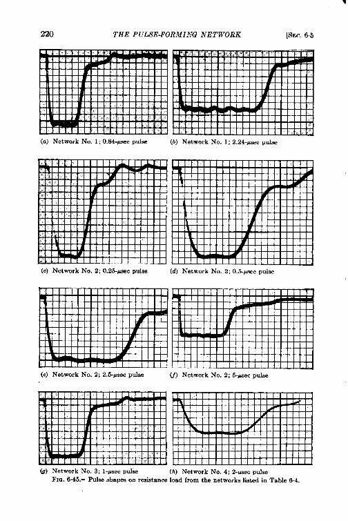
220 THE PULSE-FORMIi’?G NETWORK [SEC. 6.5
(a) Network No. 1; 0.84-@ec pulse (b) Network No. 1; 2.24-psec pulse
(c) Network No. 2; 0.25-@ec pulse
1
I I t 1 i I I I I I,11!
1I
1.I ,
(e) Network No. 2; 2.5-#see pulse
1 I 111[ 11 I n-rl-l I 1~’ I 1 I I i
, I rIi 1 1 I 1 , r I ,H++++tw-h ,.,.,..dtl-ttm1 1 1 1 I I I I I I I 1 I
ttu.L_. ._! Ili I II
(f) Network No. 2; 5-Wee pulse
(p) Network No. 3; l-psec pulse (h) Network No. 4; 2-usec pulseFIG. 6.45.—Pulse shapee on resistance load from the networks hated in Table 6.4.

SEC. 6.6] TEST PROCEDURES 221
The construction of network N’o. 3 maybe considered as typical of thatemployed in the majority of type E networks. It is housed in a terne-plate can \vithmetalized glass bushings. The can is of sufficient resiliencyto take care of differential expansion. The five condenser sections aredesigned to distribute the voltage effectively by four series sections andto minimize the inductance arising from the lead connections. Thegradient is approximately 210 volts per roil. The condenser sections areheld bet\veen bakelite end plates by means of metal bands. The totalcapacitance of the net\vork is adjusted so that it will be within t 5 per centof the rated value after impregnation.
The inductance consists of two close-wound coils wound on a +in.ba’kelite form. The input inductance is wound with 32 turns of N’o. 22enameled wire and is mounted separately from the main coil, whichconsists of 26, 26, 26, and 31 turns of the same size wire. Although theinput inductance must be separated from the other inductances becauseof the choice of can size and shape, it is possible to obtain a satisfactorywave shape on resistance load. The coils are mounted in a bakelite framethat can be attached to the end plates of the condenser bank before theassembly is placed in the can.
6.6. Test Procedures. -The electrical tests to which networks aresubjected include a voltage-breakdo\vn test, an insulation-resistancetest, and a dissipation factor test; tests involving the determination ofpulse dllration, rate of rise, general pulse shape and impedance; and,
finally, determinations of the temperature rise (w-hich is a measure of
efficiency) and life of the unit under normal operating conditions. Only
those tests designed specifically for net!vorks are described in this section.
For temperature-rise and life tests, the network is operated undernormal rated conditions in a pulser of a type similar to that in \vhich it isto be used. Tests are conducted at both the maximum and minimumratings for continuous operating temperatures, as ll-ell as at normal roomtemperature.
The impedance of a network may be measured in se\’eral TraysProbably the most obvious method is to discharge the network into apure-resistance load through a bidirectional switch and to adj~lst theresistance until no reflection is obtained after the pulse, The resistanceof the network is then equal to the load resistance. The main dra\vbackof this method is that it introduces an unknown qllantity, the switchresistance. This difficulty can be avoided to a certain extent by the useof a long cable \vhose impedance has previously bern dctrrmined hy othrrmethods, but the possible difference in its impe{kmce under pulse and r-t’conditions makes this expedient of doubtful value. In addition, thevoltage of the first step is related to the voltage of the main pulse by
1By J, V. Lebacqz.
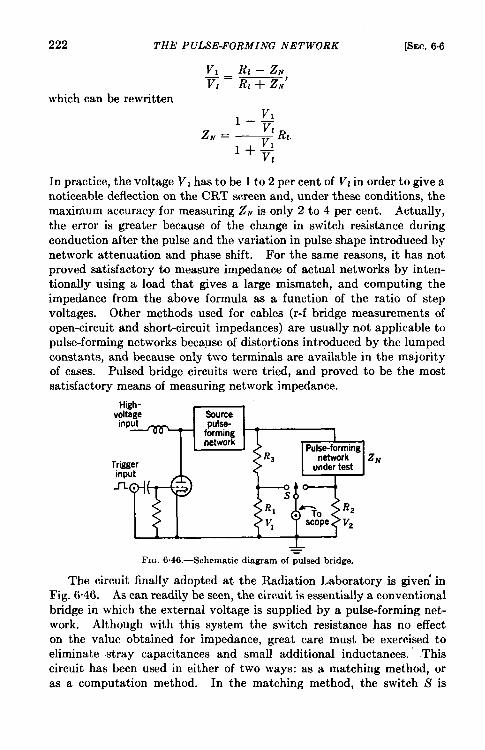
222 THE PULSE-FORMING NETWORK
v, Rl – .ZN-Tl= mN’
[SEC. 6.6
which can be rewrittenv,
l–EZ. =~ R1.
l+T1
In practice, the voltage V, has to be 1 to 2 per cent of VI in order to give anoticeable deflection on the CRT screen and, under these conditions, themaximum accuracy for measuring Z. is only 2 to 4 per cent. Actually,the error is greater because of the change in switch resistance duringconduction after the pulse and the variation in pulse shape introduced bynetwork attenuation and phase shift. For the same reasons, it has notproved satisfactory to measure impedance of actual networks by inten-tionally using a load that gives a large mismatch, and computing theimpedance from the above formula as a function of the ratio of stepvoltages. Other methods used for cables (r-f bridge measurements ofopen-circuit and short-circuit impedances) are usually not applicable topulse-forming networks because of distortions introduced by the lumpedconstants, and because only two terminals are available in the majorityof cases. Pulsed bridge circuits were tried, and proved to be the mostsatisfactory means of measuring network impedance.
High-voltaRe ~
inp~t puls4-formingnetwork 1-
TTi!_rriggerinputJ-L . ---
{R3&’NmsRI
.-ToR2
v, scope V2
+FrQ. 6.46.—Schematic diagram of pulsed bridge.
The circuit finally adopted at the Radiation Laboratory is given’ inFig. 6.46. As can readily be seen, the circuit is essentially a conventionalbridge in which the external voltage is supplied by a pulse-forming net-work. Although with this system the switch resistance has no effecton the value obtained for impedance, great care must be exercised toeliminate stray capacitances and small additional inductances. ” Thiscircuit has been used in either of two ways: as a matching method, oras a computation method. In the matching method, the switch S is

SEC. 6.6] TEST PROCEDURES 223
a commutator and RI is made equal to R2. The resistance lh is thenvaried until the traces of the voltage across RI and Rz appear super-imposed on the CRT screen through the action of the switch S, as indi-cated in Fig. 6.47a. The value of Z~ is then equal to R3.
In the computation method, all the resistora are fixed, and the valueof ZM is easily obtained by measurement of the voltages VI and Vzbecause
The matching method is more convenient for the routine checking ofnetworks. Difficulties are apt to arise, however, because of the induct-ance unavoidably introduced in building a variable resistance capable of
(a) Os.illogram showing balance of ir- e(b) OsciUogram showing effect of non-pedance in puked bridge. Trace A is ob- inductive resistor in pulsed bridge. Tracetained from the network arm of the bridge A is obtained with an inductive resistanceand trace B from the resistance arm. and trace B with a noninductive reeietance.
FIG.6.47.
withstanding the power and voltage requirements. In the setup thathas been used at the Rdation Laboratory, the resistor consists of non-inductive elements connected through three selector switches to enablevariations in steps of 10, 1, and 0.1 ohms. The additional connectionsnecessitated by this system result in the appearance of oscillations onthe top of the pulse, as indicated by Fig. 6“47b. This figure shows thewave shape through the resistance arm of the bridge only; the smoothertrace corresponds to use of a noninductive resistance for Ra, the other cmeto the use of a variable resistance for Rs. The two resistors were equaltowithin 0.1 ohm.
The choice of the best possible pulse-forming network for the sourcestill remains to be discussed. Experience has indicated that the valueobtained for the-impedance of the network under test depends slightly on

224 THE PULSE-FORMING NETWORK [SEC. 6.6
the characteristics of the source. It is necessary to keep the resistancesRI and R2 small in order to produce the desired amount of deflection onthe scope if the measurement is to be made at a power level comparableto that for which the network is designed. Thus, if the two networkshave very nearly the same impedance, the source network is workinginto a load impedance that is considerably smaller than its own imped-ance. It has also been observed that this amount of mismatch has aneffect on the oscillations on the top of the pulse. Figure 6.47a indicatesthat the response of a network and of a resistance to the leading edge ofthe pulse is not the same. In view of this fact, it is probably desirable touse for a source network one that has an impedance approximately equalto that of the load and whose other characteristics correspond, as nearlyas possible, to those of the network under test. In order to meet theseconditions, however, a large number of special source networks arerequired. In practice, either a network of the same series, or one ofapproximatee]y the same pulse duration and impedance as the one undertest, is used.
The values of impedance obtained by pulsed-bridge methods can beduplicated easily with a circuit of the same type. Any discrepancies inthe results that are obtained by the two methods (these discrepancieshave been as high as 5 per cent) are caused chiefly by the inductance ofthe adjustable resistor that is used in the matching method,

THE
CHAPTER 7
DISCHARGING CIRCUIT OF THE LINE-TYPE PULSER
BY J. V. LEBACQZ
7.1. General Properties of the Discharging Circuit.—The basiccharacteristics of the discharging circuit are determined entirely by theelements making up that circuit: the pulse-forming network, the switchtube, and the load. A pulse cable and a pulse transformer are oftenadded between the pulser and the load although they are not essentialto the operation of the equipment. The pulse cable is usually addedonly for convenience in engineering, and for greater flexibility in thephysical location of the pulser and the load. The pulse transformer, onthe other hand, can often be considered a necessary component of thepulser because it reduces the maximum network voltage that is necessary,and thus eases the problems of switching. As a result, the design prob-lems are simplified, and a saving in weight and an increase in reliabilityare generally effected. The introduction of a ~ulse cable and a pulsetransformer also affects the general characteristicsof the discharging circuit.
The general properties of the discharging cir-cuit can conveniently be arrived at by consideringthe simple circuit of Fig. 7.1.
As has been seen in Chap. 6, a charged loss-Iess transmission line produces a rectangular pulseof energy if it is connected through an ideal switchto a pure resistance equal in magnitude to thecharacteristic impedance of the line. In practice,
! 1FI~. 7.1.—Si m pl e
however, the pulse-forming networks do not dupli- schematic diagram of the
cate exactly the pulse shape obtained from a loss-discharging circuit for aline-type pulser.
less transmission line.
The switch in a line-type pulser is not required to open the circuit at
the end of the pulse because the current ceases to flow when all the energystored in the pulse-forming network is dissipated. This importantproperty of the circuit makes it possible to take advantage of the highcurrent-carrying capacity and low voltage drop that are characteristic ofgaseous-discharge switches. The mechanism of the, switch operation hasan important effect on the operation of the circuit, as is discussed later.
225

226 DISCHARGING CIRCUIT OF THE LINE-TYPE PULSER [SEC. 7.1
The loads to which pulsers must supply power are not, in general,pure resistances. For most radar applications, the oscillator tube canbe considered as a biased diode, as is already shown in Chap. 2 (Fig.2.1 1). Random variations in the values of either the bias voltage orthe dynamic resistance may occur from pulse to pulse or during a single
pulse, and their effect on pulser performanceZ. must be considered.
r
Some of the characteristics of the circuits —&~—
RIcan be determined by considering the dis-charge of a lossless transmission line ofimpedance ZOthrough a resistance R1. Con-
Fm. 7.2.—Ideal discharging sider the circuit of Fig. 7.2, in which thecircuit for a line-type pulser.
switch can be closed instantly, and is assumed
to have zero resistance when closed. If the line is charged to a potentialVO,the current in the load after closing the switch is given by
v,i(t) = Z. + R1
[— l–u(t–26)– = [U(t – Za) – U(t – 46)]
()+ =, 2 [U(t – 43) -
1“U(t – 66)] – “ . . , (6.7)
whereU(At) = 1 for At >0,U(At) = O for M <0,
At = (t – m$, n = 2,4,6,...
In general, only the energy transferred to the load during the firsttime interval 26 is of practical value, and in that case,
1Il=VO————
RI + ZO(1)
and
Vt = v, +0 (2)
The pulse power in the load is
v%“ = ’21’= (R, + z,)’ ‘2’
and the energy dissipated in the load is
vi‘[ =‘r = (R, -I- Zci)2 ““
(3)
(4)
where r = 26 is the duration of the pulse at the load. As can immediatelybe seen from the foregoing equations, the pulse power and the energy

SEC. 7.1] PROPERTIES OF THE DISCHARGING CIRCUIT 227
dksipated in the load per pulse area function of the load resistance. Thevalue of load resistance for maximum power transfer can be obtained bydifferentiation of Eq. (3);
and the maximum power transfer is obtained when
Rl = 20. (5)With this condition,
11 = $, (6)
VI = ;, (7)
Pl=~ (8)
and
wl=~T. (9)
The value of load resistance for maximum pulse power given by Eq. (5)could have been anticipated from physical considerations; Eqs. (1) to(4) apply only for the first interval 26. If the load impedance equals theline impedance there are no reflections, and all the energy stored in theline is dissipated in the load during the interval 23. Any mismatchcauses part of the energy to be dissipated in the load after the time 26,and thus results in a decrease in power during the main pulse.
1.0
0.5
00 0.5 1,0 1.5 2.0
R1/ZO
F1m 7.3.—Effect of load mismatch on power transfer.
Fortunately, exact matching of the load to the transmission-lineimpedance is not particularly critical from the standpoint of power trans-fer, as long as the mismatch does not exceed 20 to 30 per cent, as can be

228 DISCHARGING CIRCUIT OF THE LINE-TYPE PULSER [SEC. 7.1
shown by taking the ratio of the power into any load resistance Rt tothe power into a matched load 20. This ratio is
v:
P.r _ (R, + Z,) ’R’ = ~ ~, 1P., – v% 20
()
R, 2(lo)
420 l+ZO
The values obtained for Eq. (10) are plotted in Fig. 7.3, showing the flat-ness of the curve near the maximum. As an example, the values ofRJ20 for which 3 per cent of the energy stored in the transmission line isdissipated after the time 26, equal to the pulse duration ,, are found rLSfollows:
R,
1 – 0.03
1= 0,97 = 4 ‘0
()
~+gl”20
(-)
R,– 1.42,zo, –
(-)R,20 2
= 0.70.
Thus, from power considerations alone, the matching of the load to theline impedance has very little effect on the discharging circuit, since only3 per cent or less of the energy stored in the transmission line is not tlis-
sipated in the load if the load impedance varies from 70 to 142 per centof the transmission-line impedance.
The energy dissipated in the load lmdcr matched conditions is eq(lalto the energy stored in the transmission-line capacitance before the pu]+e,or
which gives the fundamental relation
T = 2COZ0. (11)
The pulser design is affected by the pulse-pmvrr fin(l energy-lwr-p~ilsrmquircmcnts in sevrral \\ays. I;qllation (8) shoits that the ])(lIs( t~lltp~ltis proportional to the square of the Voltage 011the transnlisit)l~ Iinr ornct\vork, and in~’crsely proportional to the line or ncl ii (irk im~mlancc.I~ig~lre74 gi~m the maxin~~lnl p(llsr po\vcr I’zOtll:~t can IN cx~xrtcti froman ideal p(llser for variolls line impedances and voltages.
If nearly matrhwl con(iitions arr to lw rc:llizc(t, it ran he seen that thevoltage necessary to s(lpply a high pl]lsc polver to a l~igl~-il~~~lecl:~nceIOMIbecomes prohibitively high. For example, for a pulse-pm~er require-

SEC. 7.1] PROPERTIES OF THE DISCHARGING CIRCUIT 229
ment of 1 hlw into an 800-ohm load, the theoretical transmission-linevoltage is60kv. Thepractical figure ishigher because thelosses in thedischarging circuit have been neglected. A slightly lower networkvoltage can be used if the line and the load are intentionally mismatched
4,000 I II I //{ /
2,000
600 v A/
+%
400 /
/
FIC-.7.4.—,Maximum pulse power output vs. transmission-line voltage at various imlevels.
>edance
because the power transfer is not seriously affected. In practice, UP toabout 40 per cent mismatch can be tolerated (RJz, = 1.4), and under this
condition, the line impedance is approximately 600 ohms with an 800-ohmload, and the voltage is 50 kv instead of 60 kv.
Handling voltages of this order of magnitude presents serious engineer-ing problems. The most important problem is that of securing a suitableswitch. Gaseous-discharge switches are not readily suited to the very

230 DISCHARGING CIRCUIT OF THE LINE-TYPE PULSER @EC. 7.1
high voltages required in the high-impedance circuit. Neither wouldthese circuits use the high current-carrying capacity of these switches tothe best advantage. On the other hand, vacuum tubes have a high effec-tive resistance, and the losses that occur when these are used as switchesin high-impedance line-type pulsers result in low efficiency.
The small storage capacitance that results from the use of a high-impedance transmission line or network leads to other di%iculties. Thiscapacitance is given by CO = r/2Z0 [Eq. (11)] and, for a given pulseduration, decreases proportionally to the increase in line impedance.Assuming, for example, an 0.8-~sec pulse and an 800-ohm transmissionline,
co = 0.8 X 10-62 X 0.8 X 108
= 500 pgf.
The small transmimion-line or network capacitance may prove a serioushandicap in the design of the charging circuit because a charging diodewith peak inverse voltage greater than 30 kv is required to prevent thesize of the charging inductance from becoming prohibitive. Also, theconstruction of the network itself presents very serious problems becausethe network inductances increase proportionately with the impedance,and the effect of distributed capacitance on wave shape becomes pro-portionately greater as the total active network capacitance is decreased.
In spite of these difficulties, several line-type pulsers were designed inthe early days of the Radiation Laboratory to operate directly into high-impedance loads. However, a much more satisfactory solution to theproblem was achieved by the development of an impedance-matchingpulse transformer. These pulse transformers can be used over the widerange of output power (from 500 watts to 20 Mw) required from puhwraand over a range of pulse duration from less than 0.1 to more than 5 IJsecwithout seriously affecting the shape of the output pulse. The impedanceratio of a puke transformer is essentially equal to the square of the turnsratio. For a 1-Mw pulser supplying an 0.8-psec pulse to an 800-ohmload, and using a 4/1 pulse transformer, the load RIz = 800 ohms that isacross the secondary appears across the primary as
Rg, = %& = 50 ohms.
The maximum line or network voltage is now about 15 kv and its capaci-tance
co _ 0.8 X I&g100
= 8000 ppf.
The disadvantages of a pulaer coupled directly to a high-impedance loadhave now disappeared. Another advantage in the use of pulse trans-formers is the possibility of introducing a physical separation between the

Szc. 7.1] PROPERTIES OF THE DISCHARGING CIRCUIT 231
pulser and its load. In many radar applications, it has been found neces-sary to separate the oscillator from the pulser itself—in some cases,becauw+of the physical motion of the oscillator. Under these conditions,a @jtY cable links the pulser to the load. Theoretically, pulse cablescan be made in almost any impedance range, but. practical considerationslimit their impedance to less than 100 ohms. In the United States, theW-ohm impedance level for pulse cable was standardized, and, for con-venience in matching cable to pulser when necessary, the great majont yof line-type pulsers were designed to use 50-ohm pulse-forming networks.In special applications requiring an exceptionally high-power output,however, networks of 25 and even 12.5 ohms were used. In GreatBritain, on the other hand, the network impedance was centered around80 ohms-again for convenience in cable matching.
Since the loads used in microwave radar usually have input character-istics similar to those of a biased diode, theperformance of the pulser circuit with thisload must be considered in some detail. Themethod of approach, however, can be extendedto pulser circuits with loads of any typeimaginable.
The current-voltage characteristic of a bi-ased-diode load can be represented by Fig. 7.5.For any point along the load characteristic,
~1=~1= V,+ Z1tana=V, +l~~IJ II 11 ‘
where rl is the dynamic resistance of the diode.
u“_———-
.’ I
] // ‘1
I,/’1
/l I1= I
/“ ! 1/’ I I,/ I I
~ v-
FIG. 7.5.—Voltaga-currentcharacteristics of a biased.diode load.
Under these conditions
the general expression (see Eq. (l)) for the current in the load becomes
VoII=—.
v, Vd[R; + Zo
“ ;11[’1 + z,= v, + Il(rl + Zo)’
orv.
l–ITzl=vo–~”=Ko_rl + z,
‘“1+3’Zo
(12a)
so
Rl = rl + V, &&~ (12b)
and~+zov,
v, – v. ( )V~=ILRl=m rI+V, ~, . vo~ ~’r,v”. (13)
l+Z

232 DISCHARGING CIRCUIT OF THE LINE-TYPE PULSER [SEC. 7.1
In this case, the conditions for optimum power transfer between thetransmission line and the load depend on the bias voltage as well as onthe initial voltage on the line. Substituting R1 = Z, in Eq. (12b),
(20– n) (v, – v,) = -V.(?-1 + 20),
which may be simplified toVo
20 = rl v, _ ~v,~
or2V.
v, = —.
q
(14)
(15)
Equation (15) expresses the voltage to which the transmission line mustbe charged in order that the load operate at the only point correspondingto matched conditions, or to maximum power transfer.
Then, for matched conditions,
Vl=vo+zo+and
(17)
(18)
It is seen that the expressions for current, voltage, and pulse power areidentical with Eqs. (6), (7), and (8) obtained for a pure-resistance load.
Fm. 7.6.—Simplified equivalent circuit for FIQ. 7.7.—SimpMied equivalent circuit for aa line-type pulser with a resistance load. linet ype pulser with a bked-chode load.
Expressions identical to those for the current and the voltage in theline-type pulser can be obtained from the consideration of a simple seriescircuit containing a battery of constant voltage V, and internal resistance20, a switch closed for the timer, and a load resistance Rl (see Fig. 7.6).

SEC.7.2] PULSER CHARACTERIS~ {CS
For this circuitv,
l’=Z&Rland
RlVI = Vo z, + ~1”
[See Eqs. (1) and (2).] For a biased-diode load (Fig. 7.7) of dynamicresistance rl,
v, – v,
11= Zo+qand
v,= v.+ r,v+ = qojy.
[See Eqs. (12) and (13).]Since the circuits of Figs. 7.6 and 7“7 give the same results as those
obtained by the transmission-line theory, they can be considered adequateequivalent circuits for a further discussion of the currents and voltagesin line-type pulsers. On the other hand, this circuit is not satisfactoryfor determining energy relations because ZOis not physically a dissipativeelement. The value of ZO is determined from a fundamental considera-tion of the charging of an infinite transmission line, across which a batteryvoltage is suddenly applied, and is then defined as the ratio of voltage tocurrent in the line. If the line is assumed to be lossless, the impedance,ZO = ~~~, has the dimensions of a pure resistance, hut does not dis-sipate energy. It can easil y be seen that the circuits of Figs. 7.6 and 7.7are identical with those of the hard-tube pulser discussed in Chap. 2.The principal difference lies in the ratio of 20 to Rt or T1. For mostpractical applications of line-type pulsers, ZO is very nearly equal to Rj,
v,or to rr ~. _ ~v, J whereas, in general, a hard-tube pulser is operated
with a load whose impedance is high compared with the pulser internalimpedance (effect ivel y the resist ante of the switch tube, which is dis-sipative). This difference is very important in the consideration of pulserregulation, efficiency, and the effect ofother circuit parameters on pulse shape.
7.2. P u 1s e r Characteristics. — Atypical discharging circuit for a line-type pulser can be represented bythe diagram of Fig. 78. The ideal -
FIG. 7%.-Block diagram of the dis-rectangular pulse that was considered charging circuit of a line-type pulser.in the preceding section is usually
unobtainable in practice because of the characteristics of the various com-ponents used in the circuit. Some of the effects on pulser behavior and on

234 DISCHARGING CIRCUIT OF THE LINE-TYPE PUL!7ER ~8M. 7.2
pulse shape introduced by the characteristics of the separate componentsare discussed in this and in the following sections. A brief n%umh ofthe characteristics that affect the behavior of the discharging circuit isgiven here to facilitate reference.
The Pulse-jormi~ Network.-As explained in Chap. 6, the pulse-
T
forming netwo&s used in practice can onlyproduce an approximately rectangular output-pulse on a pure-resistance load. In order tosimplify the mathematical analysis, it is aa-
FIG.7.9.—Electricalequi-sumed in this chapter that the pulse shape
valentof a pulse-formingnet- generated by the network ia either rectangularwork for the study of potsa or trapezoidal. It should be noted, however,slmpea that most practical networks also produceamplitude oscillations during the “flat” portion of the pulse-that is,between the end of the rise and the beginning of the fall. In general,these oscillations are small and are neglected. In addition, actual nebworks always have stray capacitances to ground that must be taken intoaccount when particularly fast rates of rise or fallare desired. i
For simplicity in analysis, the stray capaci- vtances to ground are lumped and connected at thecapacitance input terminal of the network. The
Lpulse-forming network can then be represented as ~ ---,in Fig. 7.9, in which the subscripts O for a Ioselesstransmission line have been replaced by N. ta t-
The Switch.-Three types of switches have been ~ti~~d~~~~~~~~~~used extensively in pulser operations: rotary of time.spark gaps, fixed triggered gaps, and thyratronz.In general, the electrical characteristics of these three types are the sameduring the main pulse or conducting period. Fixed gaps and thyratroneboth show a rapid decreaee in tube drop from time t = O (when the tubebegine to conduct), and the tube drop stays very nearly constant for the
I-Fm.7.11.—Tyw
ical switch drop asfunctionof current.
remainder of the pulse. A typioal curve of tube dropduring a pulse is shown in Fig. 7“10. The time ta re-quired for the voltage to decrease to a steady-statevalue, VP vanes with the particular switch consideredand is usually about 0.3 psec for triggered gaps, and0.1 Peec for thyratrons. For a given tube the steadyvalue of the tube droD is very nearly independent ofthe current, as shown ~y Fig. 7T11. Tie ave;age values
for VP under actual operating conditions are approximately 120 to 150volts per gap for typical fixed spark gaps, and 70 to 110 volts for typicalhydrogen tb yratrons.

Snc. 7.2] PULSER CHARACTERISTICS 235
The data taken with rotary spark gaps points to approximately thesame results as were obtained with fixed gaps or thyratrons. Rotarygaps, like thyratrons, have been used successfully at pulse durations ofthe order of magnitude of 0.1 Ksec, indicating a very fast decrease involtage drop across the gap after the initiation of conduction. .Althoughthe time jitter of the rotary gap does not directly affect the dischargingcircuit, it may affect the final charging voltage of the network. Underunfavorable conditions, the resulting change in power output from pulseto pulse may be several per cent.
The principal difference that is introduced in the behavior of the cir-cuit by the switches occurs immediately after the pulse. Rotary gapsand triggered fixed gaps are essentially bidirectional devices, but thethyratron is unidirectional, and therefore holds off any negative voltageappearing at the plate aa a result of impedance mismatch. This facthas a definite effect on the shaping of the tail of the pulse, causing post-pulse conduction for bidirectional switches and a higher voltage back-swing for the thyratron switch. Different principles of circuit-elementprotection must also be applied because of dif-ferences in the switches. ninaty L/.
The Pulse Transformer. -An equivalentcircuit adequate for the discussion of the effect
n
LD
of pulse transformers is derived in Sec. 12”1, Cf,and is given in Fig. 7“12 for reference. Tomake the analysis easier, however, further Fm. 7.12.—Equivalent circuit
for a pulse transformer.simplifications are usually introduced, andthose circuit elements that have little effect on the particular portion ofthe pulse under consideration are neglected.
For simplicity, it is assumed in the following discussions that anypulse transformer introduced in the circuit having a voltage stepup ratioof n is replaced by a 1/1 transformer, and equivalent circuits for line-typepulsere are all referred to the secondary of the pulse transformer. Underthese conditions, the actual primary voltages are multiplied by n, theactual primary currents are divided by n, and the actual impedances aremultiplied by n2, that is,
Rw = ntRti,
Lw = n2LP~,
CM= -j C&i.
The assumption that the losses in the pulse transformer are negligible issufficiently accurate for discussions of pulse shapes, and is warranted bythe simplifications it introduces in the mathematics. When the losseshave to be taken into account, it can be assumed that the voltage trans-

236 D18CHARQING CIRCUIT OF THE LINE-TYPE PULSER ~8Ec. 7.2
formation is conserved, that is, the ratio of primary to secondary voltageis equal to the ratio of the number of turns in the pulse transformer. Thelosses then appear as shunt losses and aflect the ratio of currents andimpedances as follows:
V- = ?’lVd,
where q~is the efficiency of the pulse transformer.The Load. -As previously stated, the load most widely used in radar
applications of pulse generators has the characteristics of a biased diode.In addition, a certain amount of capacitance is usually present in parallelwith the load, and its effect on the leading and trailing edges of thepulse must be considered. Although the scope of this chapter does notpermit a specific study of all the possible types of pulser loads that canbe used, an important special application of the circuit has been found inthe triggering of series gaps. In this case, the puke shape is relativelyunimportant, and the load is essentially a pure capacitance until thebreakdown of the gaps, at which time the load is short-circuited. Thisparticular case is considered in Chap. 8.
Equivalent Circuit for a Line-type Pulser.-A complete equivalent dis-charging circuit for a line-type pulser, obtained from the above considera-tions,l is shown in Fig. 7.13.
-.Fxc+.7.13.—EquivrJent diechsrting circuit for a line-type pulser.
For the remainder of this section, further simplifications can be madem this circuit. First, the output-power pulse is considered to be rec-tangular, even though it is shown in Sec. 7.4 that a perfectly rectangularpulse is unobtainable in practice. It is therefore necessary to define thepulse duration. In general, the pulse duration of any shape pulse is con-sidered here to be that of a rectangular pulse that has an amplitude equalto the average amplitude (see Appendix B) of the top of the pulse under
1The seriesreaistsnce R= includesthe equivalentswitch resistanceand the serieslossesin the networkand pulsetransformer.
SEC. 7.2] PULSER CHARACTERISTICS 237
consideration, and that delivers the same amount of energy to the loadas does the pulse under consideration. Then the equation
L
T.Vtildt
o~=V1.zl
gives the equivalent pulse duration, where V1 and 11 are the amplitudesof the voltage and current pulse averaged over the top of the pulse, andV1and ii are the instantaneous values of voltage and current.
The general circuit that is of interest in this discussion includes thelosses of the components that make up the circuit. With the abovedefinition of pulse duration, however, it is not necessary to refer to theactual pulse shape in order to determine the power and energy relation-ships; instead, the equivalent rectangular pulse is considered. Theequivalent circuit of Fig. 7.13 can thus be further simplified by the fol-lowing assumptions:
1.
2.
3.
4.
The series inductances are neglected, since no voltage can appearacross them during the “top” of a rectangular load-current pulse.The time constant of Z~ and CD is considered to be so small com-pared with the pulse duration that the charging time of CD, andtherefore C,, itself, can be neglected.The voltage drop across Z~ and the series resistances produced bycurrent flowing through L. is considered to be negligible, since theoutput current pulse is assumed to remain rectangular in sha~e,and- thus L. can ‘also be neglected.
(a) Switch resistance is independ- (b) Switch drop is independent ofent of current. current.
FIG. 7.14.—Equiva1ent circuits for the study of power transfer.
The series losses produced by the switch, network, and pulse trans-
former can, in general, be lumped into one resist ante R,, as indi-cated in Fig. 7.14a. This assumption is equivalent to saying thatthe switch has a constant resistance that is independent of thecurrent. In cases where the switch drop is not very small (lessthan 10 per cent) compared with the network voltage, it is prefer-able to assume that the switch has a constant voltage drop VP,

238 DISCHARGING CIRCUIT OF THE LINE-TYPE PULSER [SEC.7.2
as indicated in Fig. 7“14b. In this case, the value of the seriesresistance is represented by R;.
Pulse Power, Power Transfer, and Load Line.—If the case of a resist-ance load, for which V, = O and rl = Rz, is considered first, the current inRi corresponding to Fig. 7.14a is given by
or
which can be written
‘l=zN(l++)+;(lIntroducing the coefficients
=l+ZN+R,a
R,
andR,
~=l+z
Eq. (19) becomes
11 =VN
Z@ + Rla”
A comparison of this expression with Eq. (l),
v,11=—
Zo + RI’
(19)
(20)
(1)
indicates that the load current is reduced by the losses in the circuit,since VO and ZO are equivalent to VN and ZN respectively (the subscriptzero refers to lossleee transmission lines and the subscript N to actual net-works). For this reason, the coefficients a and @ are referred to as“loss coefficients,” a representing the shunt losses, and f3the series losses.
From Eq. (20), the load voltage is given by
V1= VNRZ
zNB + Ria(21)
and the pulse power byV~Rl
‘1 = (ZN13 + R,a)’”(22)

SEC. 72] PULSER CHARACTERISTICS 239
The relation between Rl and Z. for maximum power transfer into theload for a given network voltage can again be found by differentiatingEq. (22), and equating the result to zero; thus
dPl v; V$R&
~ = (zN@ + Rla)2 – (ZN~ + Rla)’ = 0’
orZM9 + Rla – 2RUZ = O
RL = ZN $ (23)
Equation (23) showB that, when 10WS are taken into account, the maxi-mum power transfer to the load is obtained for a value of load resistancethat is different from the characteristic impedance of the network. Ifonly series losses exist (R. = ~), ~ximum power transfer is obtainedfor a load resistance that is equal to the network impedance plus theresistance corresponding to the series 10SSWJ, that is, Rt = ZN + Rp
If onJy shunt losses exist (IL. = 0), the value of load resistance for maxi-mum power transfer must be equal to the equivalent resistance of thenetwork impedance and shunt-loss resistance in parallel, that is,
Rl =ZNRe
ZN + R.”
In general, the series and parallel losses are of the same order of mag-nitude (a = /3). Therefore, it is usually sufficient to make ZN equal toRl, and the departure from optimum power transfer is not great becauseof the flatness of the power-transfer curve (Fig. 7.3). When the condi-tions for maximum power transfer are realized for a resistance load, theexpressions for load voltage, current, and power are
The load current, voltage, and power are easily obtained by the samemethods from Fig. 7. 14b if VN is replaced by VN — VP) Rp by R;, a by a’and # by b’, giving
11= ‘: -v’,,zNb + Rw
(27)
– VP)RZVJ = (;N;, + Rw, J (28)

240 DISCHARGING CIRCUIT OF THE LINE-TYPE PULSER ~SEC. 7.2
and
P,=( v. – V,)2RZ
(zN@’ + lid)”
The mruimum power that can be delivered by the circuit is
(VN – v,)’-(WCU = ~zNa,fi,
(29)
(30)
The principal reason for a representation of this type in the study ofthe obtainable pulse power is to emphasize the effect of tube drop in thedesign of low-power pulsers. As long as the tube drop is only a few percent of the network voltage either presentation is adequate. However,the rapid increase in losses, arid the corresponding decrease in availablepower as the switch drop increases, are more evident from Eq. (3o) thanfrom Eq. (26). For instance, if Vp is about 10 per cent of VA.,the 10WSin the switch amount to nearly 20 per cent of the load power.
In Fig. 7.4 a series of curves for P,, = ~/(4ZJ are plotted. Thesame curves can, of course, be used to represent Eq. (26) if the coordi-nates are made to represent [ad PJJ and VM instead of P%, and VO, orEq. (3o) if the coordinates are changed to [a’B’(Pi)_] and (VN – V,)
respectively.If the load is considered in the more general terms of a biased diode of
instantaneous static impedance
E, = v. + InI, ‘
the expression for load current [Eq. (20)] becomes
This equation can be rewritten as
Viv – Vsa1’= Z./l + T@’
which is of the same form as Eq. (12).With the value of 11 from Eq. (31), the voltage across the load,
VI = Iml + V,,becomes
V1 = VNrl + V.ZN/3zAf3+ rw ‘
and the pulse power is
p, = Vlrl = (v.r~ + V,ZNB)(VN – V.a)o(ZM9 + m)’
(31)
(32)
(33)
SEC.7.2] PULSER CHARACTERISTICS
Maximizing the power as a function of TJ,it is foundvoltage giving maximum power transfer to the load is
241
that the network
(34)
A comparison of Eqs. (15) and (34) shows that when the losses in the cir-cuit are considered, the voltage on the network for maximum load poweris greater than that obtained when the losses are neglected, by a factorapproximately equal to a. The same expression may be obtained bymaximizing the power as a function of V., or by introducing the expres-sion for static impedance of the biased diode into Eq. (23) and usingEq. (31). It is therefore evident that there is only one operating pointfor a nonlinear load where maximum power is obtained and, accordingly,that there is only one definite value of network voltage that leads tooperation at that point. It is fortunate that the circuit performance isnot greatly affected by slight deviations from the conditions giving maxi-mum power transfer.
To demonstrate this point, Eq. (33) may be rewritten to express thepulse power as
By introducing Eq. (34) into Eq. (33), the pulse power corresponding tomaximum power transfer is found to be
(35)
The power-transfer relation PJ(P& can be expressed as
.’a,(%+w+)(P;’w
(“+5”) ‘“ ‘3’)
When V,/VN equals zero, the special case of a pure-resistance load isobtained. For any value of VJVN greater than l/a, the power outputdrops to zero because the expression gives a negative value for powerunder this condihion. The curves of Figs. 7.15 and 7.16 indicate theeffect of the losses in the circuit on the conditions required for optimumpower transfer when the 10SScoefficients have the values 1.0, 1.1, and 1.2,

242 DISCHARGING CIRCUIT OF THE LINE-TYPE PULSER ~~EC. 7.2
1.0
1.0
0.9\
~ 0.8
s 1.04-
A0.9 I
0.8a=~=l.o
IzEEI?0 0.2 0.4 0.6 0.8 1.0 1.2 1.4 1.6
r,/zNFua. 7. 15.—Power-transfer curves for various values of V./ VN, a and8.
0,:
0.4
0.3
-“ ,
0.2I
a=(f=l.20.1
a=l.2
o0.1 0.2 0.3 0.4 0.5 0.6 0.7 0.8 0.9 1.0
~/zN
Fm. 7.16.—Relation between V,/VN and rijZN for maximum power transfer for variousvalues of 10ss coeficienta.

SEC. 7.2] PULSER CHARACTERISTICS 243
which cover the range ordinarily encountered in line-type pulsers. Thesecurves also show that very lit tle loss in power results from a slight mis-match, as was already determined in Sec. 7”1 (Fig. 7“4) for a resistanceload and a lossless circuit. More important, these curves show thrvt, inorder to achieve maximum power transfer, the dynamic resistance of theload must decrease as the bias voltage is increased. This phenomenoncan best be explained physically by a consideration of the load line of thepulser, a curve that gives the relation between output current and outputvoltage as the load resistance is varied, all other conditions remainingthe same. Referring to the expressions (20) and (21), and eliminatingRl between them, there is obtained
(37)
which is the equation for the pulser load line plotted in Fig. 7.17. Byinspection of this equation, it can be seen that the open-circuit load volt-age is VN/CY, the short-circuit load current is VN/(ZN@), and that the
Fm. 7.17.—Diagram showing the determination of the load voltage and current by theintersection of the load characteristic line with the pulser load line.
function is linear. The load characteristics can be represented on thesame plot; thus a resistance load is represented by a straight line passingthrough the origin, whereas a biased-diode load is represented by astraight line intersecting the V axis in the positive region. The inter-section of the pulser load line with the Ioad characteristic line gives theoperating point. A load characteristic line has been drawn for
()Rl = ; z.,

244 DISCHARGING CIRCUIT OF THE LINE-TYPE PULSER @EC. 7.3
corresponding to optimum power transfer from the pulser to the load.Its intersection with the pulser load line at point A corresponds to avoltage VN/(h) and a current VN/(2ZN19), the only point on the loadline for which optimum power transfer obtains. Conversely, any loadwhose characteristic passes through that point enables the pulser tooperate under the conditions of maximum power transfer.
Such a load could be the biased diode represented in the Fig. 7.17.It is evident from Eq. (36) that, unless negative resistance is considered,the highest value of bias voltage that permits operation at point A isV~/(2a) (see Fig. 7.16). It is also apparent that the higher the biasvoltage on the diode, the steeper the load characteristic must be if itis to pass through point A. This condition corresponds to a smallAV/A1 or dynamic resistance, and explains why the maxima in thecurves of Fig. 7-16 shift toward small values of rz/Z,v when V,/VN isincreased.
7.3. Pulser Regulation and EfEciency.-Pulser regulation refers tothe changes in pulser output voltage, current, and power resulting fromchanges in operating conditions. These changes may take place eitherduring a pulse or from pulse to pulse. The present discussion neglectsthe circuit inductances and stray capacitances, and is valid as long asthe “transient regulation” is not considered. The results thereforeapply to the cases where a change in circuit parameters has taken placebetween two pulses, or, if the change takes place during the pulse itself,the results are valid only after any transient effects have been dampedout.
There are two types of regulation to be considered: (1) that producedby changes in the network voltage, and (2) that produced by changes inthe load characteristic. In either case, transient regulation may appear.The effect on the pulser output of possible oscillations or irregularitieson the top of the input voltage pulse can be analyzed only by methodssimilar to those of Sec. 7.4 used in studying pulse shape. If, on theother hand, the load characteristics suddenly change during a pulse,the transient behavior from one characteristic to the other depends onthe values of the distributed capacitance across the load as well as on theseiies inductance introduced by the pulse transformer.
Neglecting transients, the circuit of Fig. 7.14 can be used for thestudy of regulation, leading to the expressions for load voltage, current,and power obtained in Sec. 7.2, namely,
V1 = vNrt + V,ZNB,zN~ + rl~
VN – V,.
lZ = zNj3 + ?la’
(32)
(31)
SEC. 7.3] PULSER REGULATION AND EFFICIENCY H5
andPI = (~,vr, + ~szN6) (VN – t’ad,
(z,vj3 + r,a)’(33)
The regulation may be obtained from these equations by differentiation.Regulation against Variations in Network Voltage.—The voltage regu-
lation is obtained by differentiation of Eq. (32), which gives
dl’1 rl— = ZJ3 + rla”dV~
Multiplying by dV.v, dividing by VI, multiplying numerator and denom-inator of the right-hand member by V., and replacing the differentialby a finite difference, there results
For operation at maximum power transfer,
v,1 – ;;,
K= 2a (34)
and the expression for voltage regulation becomes
The expressions for current and power regulation are obtained in thesame way, with the following results:
()All 1 AV.~,w= V. VN’
l– F.”
(40)
and
(HAPi 2+*(+’-”) AVN ,4,,PI ““ =
1++(%’-”)-(+)%’=”
For the case of maximum power transfer, these equations may be sim-

246 DISCHARGING CIRCUIT OF THE LINE-TYPE PULSER [%C. 7.3
plified to
and
(-)AR z AVN?’1 ,N= VN”
(42)
(43)
For a resistance load, V, = O, and the expressions for regulation reduceto
(-)AVt _AVNVI VN= VN’
(44)
(-)AIz _ AVN,
11 ,. VN(45)
and
(-)API = ~ AVNPI v“ VN ‘
(46)
whether or not the load resistance is matched to the characteristicimpedance of the network in order to obtain maximum power transfer.
An examination of expressions (38) and (40) shows that, for a biaseddiode, the load voltage always changes less rapidly than the networkvoltage, whereas the load current changes more rapidly. For instance,assuming zN/rl = 10, a = @ = 1, and maximum power transfer, Eq.(39) gives
(-)
AVZ = 2 ‘V~ = () 182 ~,vi VN iim “ vii
and Eq. (42) gives
()
AIL 2 AVN AVNz v“
mm=1“82 m“
The value of V./VN corresponding to the above assumptions is 0.45(Fig. 7“16). It(made smaller)v,/vN = 0.4,
must be noted that the current regulation is improvedif the ratio of V./VN is decreased. For instance, for
It is interesting to note that the output-current regulation against achange of network voltage depends only on the ratio V,/VN. It is alsoworth noting. that, since the network voltage is directly proportional tothe input voltage to the pulser circuit, V,v can be replaced by EM inthe above expressions. This fact is important in pulser design, where

SEC. 7.3] PULSER REGULATION AND EFFICIENCY 247
tolerances on the input voltage are usually known. For alf practicaloperating conditions of magne ron load encountered to date, V,/ Vx isin the neighborhood of 0.4 to 0.45, and hence the percentage change inmagnetron current resulting from pulser regulation alone is approximately1.75 times as great as the percentage change in input voltage.
Regulation against Variations in Load Characteristic. -Two typesofregulation of the pulser output against load variation are discussed here.First, it is assumed that the bias voltage, V,, of a biaseddiode load maychange either from pulse to pulse or ‘during a pulse, but that the dynamicresistance, rl, stays constant (this case corresponds quite closely tomode-changing in magnetrons). The expressions obtained for this case
—a
()AIl = Z,vp + T@ ‘“ AV, = 1 AV,z v, V.–v,a “T ~ VN1” W’.—.
Z.@ + T@ v, aand
()APl——. —
-E V,=(‘iii%”)”%
(47)
(48)
(49)
For operation at the point corresponding to maximum power transfer,the expressions for regulation against load bias voltage become
1rl CY
()
—— -AVI Z.V B AV,.—Tr V.= rl a v. ‘
1+~~
and
It is obvious that the power regulation at the point of matched condi-tion is perfect—that is, a small change in load bias voltage around thatpoint produces no change in power output from the pulser—since the
248 DISCHARGING CIRCUIT OF THE LINE-TYPE PULSER [SEC. 7.3
tangents to the power-transfer curves (Fig. 7“15u) are parallel to theV,/V. axis at the points of maximum power transfer (matched condi-tions). For the same reason, the values of voltage and current regula-tion must be equal, but of opposite sign. For ZN/rl = 10 and a = ~ = 1,
()AVZ 0.9 AV. _ 082 ~,.mv. =fiv. “ ~.
The second case to be considered is that in which the bias voltage,V,, stays constant, but the dynamic resistance varies. Of special interestis the condition V, = O, giving the regulation as a function of load varia-tion for a pure-resistance load as
and
(50)
(51)
(52)
For operation at maximum power transfer,
()AVL 1 AM.——% R, 2R1’
()AIz 1 AR1——,~ R,
=–2R,
and
()APJ~ R,
= o.
It must be noted again that the above expressions apply only to smallvariations in the value of the load resistance. If the load variation isvery large, as in the case of an accidental short circuit at the load, it isbetter to refer to the load line of the pulser under consideration.
A special case of regulation from pulse to pulse, corresponding tothe pulser using a unidirectional switch, is considered later (see Sec. 10”2).As has already tieen pointed out, the network energy is conserved under
SEC. 7.3] PULSER REGULATION AND EFFICIENCY 249
these conditions if RJ/ZN k less than one, and the network voltage afterthe next charging cycle is higher than normal. Since a discussion of thisphenomenon involves the over-all pulser circuit it is beyond the scope ofthis section, which is concerned primarily with the characteristics of thedischarging circuit.
Eficiency.-The over-all efficiency of a line-type pulser can beobtained only by a consideration of the different parts of its circuit.Losses occur in the discharging as well as in the charging circuit. If~d and qc are the efficiencies of the discharging and charging circuitsrespectively, the total efficiency m of the pulser circuit is qP = w X q..This efficiency, however, does not take into consideration all the powerthat has to be supplied to the pulser. For d-c charging, a rectifier circuithaving an efficiency Tbusually has to be introduced. For a-c charging,the frequency of existing power supplies is such that a special motor-alternator or frequency converter is usually needed, which is also con-sidered to have an efficiency ?l*. Finally, there are overhead losses, someof which are associated with the switch and some with the auxiliary cir-cuits and equipment. The hydrogen-thyratron switch requires filamentpower and sometimes a trigger amplifier, the series~gap switch requires atrigger generator, and the rotary-gap switch requires a driving motor(whose power loss may already be included in ~b). The auxiliary cir-cuits and equipment include line-switching relays, control circuits, coolingfans, etc. If the power required for the overhead is designated as PL, theover-all efficiency is given by
m.. . _—.Vbllp‘“ = (P,).. ~ + PL?lb~~
=+PL —(P,)..
(53)
The following discussion is concerned principally with the efficiencyof the discharging circuit, with an occasional reference to the over-allpulser efficiency. The over-all efficiency for a few special applicationsis considered in Chap. 11.
The discharging-circuit efficiency is the ratio of the energy transferredto the load to the energy taken from the pulse-forming network perpulse. This definition of discharging efficiency is considered because,under some conditions of load mismatch, some of the energy may beconserved on the network when a unidirectional switch is used, as isevident from consideration of an idealized circuit (Fig. 7.2). The energydissipated in the load is given by
and the voltage left on the network after the main pulse is

250 DISCHARGING CIRCUIT OF THE LINE-TYPE PULSER @EC. 7.3
If R, > Z~, VM_l is of the same polarity as V., and the network di5charges completely even through a unidirectional switch. If Rl < Z~, anamount of energy ~CNV~_l is left on the network because a unidirectionalswitch does not permit the network voltages of polarity opposite to thatof VN to discharge. Under the latter condition, the amount of energytaken from the network is
w. = ; CN(vfi – vj_J = ; C?+vj[
~ _ (RI – z.)’
(R, + z.)’ 1
As was shown in Sec. 7.1,TN= 2CNZN,
and the energy taken from the network is
‘N = (Rl?%N)2 ‘N’
which is exactly equal to that transferred to the load, provided that71 and r. are equal. This condition is obviously attained in a circuitcontaining only pure-resistance components, such as that of Fig. 7.2.
It maybe concluded from the above considerations that it is desirableto use unidirectional switches and permit the load to be mismatched.Other disadvantages, however, result from changes in load impedance(see Sec. 10”2), and usually make it desirable to drain off most of theenergy left on the network after the pulse. Accordingly, in the remainderof this discussion this energy is considered to be lost, that is, the networkis considered to be completely discharged after each pulse.
In Sec. 7.2 it has been shown that the maximum pulse power in theload is given by
(P,)- = g $. (26)
Then, if rZ is the duration of the power pulse at the load, the maximumenergy per pulse is given by
and the energy stored in the network is
(54)
1 Vj‘N = 3 CNV$ = m. ‘N’
(55)

SEC. 7.3] PULSER REGULATION AND EFFICIENCY 251
where n and TN are the equivalent pulse durations at the load and atthe network. It must be noted that these pulse durations are not neces-sarily equal. Since the pulse power considered above is the average ofany oscillations that may be present at the top of the pulse, the effectof the inductances and capacitances is small and has been neglected.The only factor that may be significant is the voltage drop across 2.8caused by the current flowing through L. and C’D. Actually, the timeconstants are such that the effect of CDcan, in general, be neglected exceptfor the first 0.1 ~sec. In order to avoid introducing the pulse durationinto the expressions for pulse power, and because the pulse shape wasconsidered rectangular, the effect of L. has been neglected until now.
Actually, the effect of the shunt inductance cannot be neglected indiscussions of efficiency. For simplicity, however, an approximateexpression may be used. It is assumed, as before, that the voltage acrossthe load remains constant for the duration of the pulse, instead of droop-ing because of the additional voltage drop across the network impedancethat results from the current flowing through L.. Under these conditions,the current through L. at any time is given by
vl
L. ‘tL. =—,
where tis the time elapsed from the beginning of the pulse, and the energystored in the inductance at the end of a pulse of duration n is
;L.t~ = ~ 79.2L, 1
The assumption of constant voltage VI introduces a value for the lossesin the inductance L. that is in excess of the actual value. On the otherhand, any energy stored in the series inductance, L., of the circuit atthe end of the pulse is neglected because the value of this inductance issmall compared with L.. For this reason, an assumption leading tothe higher value for the losses in the shunt inductance seems to bereasonable.
The losses in the total shunt capacitance across the load C, = C. + Clappear only when the load is a biased diode, and can be written as ~C,V~.
If the inductances and capacitances are neglected, the energy outputunder the conditions for optimum power transfer is
( Wl)mu = gN’@— .
Actually, this energy output is decreased by the losses in L. and C, to
v!T2_Acp.(Wl).ff = * – —2L. 12””(56)

25!2 DISCHARGING CIRCUIT OF THE LINE-TYPE PULSER [SEC. 7.3
For optimum power transfer
vl=~
from Eq. (24),
“*=X1-H)from Eq. (34), and
(Wr)eff = *B[ –(’ -M”,N_3i&,2_gc8zM
a2L.’ a 2
Since ZN = rN/2CN, the discharging circuit efficiency can be expressed as
‘=- 1-%:-%-%37’ ‘57”)(w,).,, 1
‘d = WN afl [
where ~ = C,/C~. In general, ,1 is nearly equal to r~; therefore only avery small error in introduced by rewriting
‘d=+1-%’41-2)1 ‘57[The equation for efficiency for unmatched conditions is not given
because it cannot readily be expressed in terms of the pulser parameters;however, it can usually be determined with sufficient accuracy by multi-plying the efficiency for optimum power transfer by the actual powertransfer.
An examination of Eq. (57b) shows that the efficiency of the discharg-ing circuit decreases when the pulse duration is increased, and when ~(the ratio of distributed to network capacitance) is increased. If thedistributed capacitance is constant, -yvaries inversely with pulse duration;consequently, the third term of the expression causes a decrease in efi-ciency when the pulse duration is decreased. Since the effects of the lasttwo terms of Eq. (57a) are in opposition to each other, the curve showingefficiency as a function of pulse duration for a given set of pulser param-eters may be expected to have a maximum. The expression for theparticular pulse duration that corresponds to maximum efficiency iseasily obtained by the differentiation of Eq. (57b), and is
(58)
Assuming the usual ratio of 0.1 for rl/Z~ and values for L. and C, that arefound in typical pulse transformers and loads, the pulse durations cor-responding to maximum efficiency are found to be about 0.5 to 3 psec.

SEC. 7.3] PULSER REGULATION AND EFFICIENCY 253
Actually, the efficiency for very short pulses decreases much morerapidly than is indicated by Eq. (57) because of the nonlinear character-istic of the switch drop as a function of time. As explained in Chap. 8,a great part of the power loss in the switch occurs during the first 0.3 ~sec,and sometimes during an even shorter time. As a result, the coefficient@should actually be a function of time; however, the values obtained byexpression (57) are sufficiently correct for most practical purposes. Forvery short pulses, the efficiency obtained from Eq. (57) is usually toohigh unless a value of P that holds for these short pulses can be used.
The efficiency can also be expressed as the ratio of the average powertransmitted to the load to the average power supplied by the pulse-form-ing network. Since
(P,).. = w, x j,
and(Piv)a. = w. x f,,
the expression is the same as that obtained above. The efficiency of thecharging circuit is discussed in Chap. 9. For d-c charging, it is given as
.~==l+e2Q
2and, for a-c charging, as
Vc = 1–%
Hence, the over-all circuit efficiency q. can be obtained from therelation ~= = ~. X ?ld.
The pulser power output is usually measured by two methods. Theaverage power input into a magnetron may be represented by
(Pt).v = V2 x (12).7, (59)or by
(P,).. = v, x 12 x 71 x f,. (60)
If Eq. (59) is used, the average magnetron current is measured directlyby an appropriately protected d-c milliammeter (see Appendix A). ForEq. (60), a current-viewing resistor is used to present the current pulse onthe screen of the cathode-ray tube of a synchroscope. The averageamplitude of the top of the pulse z~, as well as the pulse duration 71 (at~lJ, is either measured directly with the synchroscope, or the area
\“’j it dt is integrated graphically from photographs of the oscilloscope.-trace. In general, readings of individual points by the two methods agreeto within a few per cent; most of the difference can be attributed to experi-mental errors and, for a large number of readings, these errors cancel

254 DISCHAkWING CIRCUIT OF THE LINE-TYPE PULSHR ~~EC. 7.3
each other. In some cases, however, a systematic difference in the read-ings is introduced, either by a small amount of post-pulse conduction,or by capacitance currents that may be recorded by the average-currentmeter, but are neglected in interpreting the oscilloscope trace. A Sys-tematic difference greater than two per cent, however, usually indicatessome fundamental difficulty with the calibration of either the sweep speed,the recurrence frequency, or the average-current meter. All three cali-brations are apt to be troublesome, those of the sweep speed and therecurrence frequency because they may vary slightly from time to time,that of the average-current meter because of the change in calibrationproduced by the shunt resistance that is usually introduced for protectionin the metering circuit.
It must be pointed out that, at best, Eqs. (59) and (60) are approxi-mate. They are rigorous only for a biased-diode load having a dynamicimpedance equal to zero because they are obtained by assuming that theload voltage stays constant during the current pulse. In general, theresults obtained from these equations are sufficiently precise as long asthe top of the voltage pulse is flat and the duration of the top of the cur-rent pulse is long compared with the sum of the times of rise and fall ofthe current. Because of these restrictions, the method is not usuallyvery precise for short pulses (less than 0.5 Psec), for which the time offall of the current is often of the same order of magnitude as the durationof the top of the pulse.
Obviously, the average-current meter cannot be used to measureaverage-power output for a resistance load, since the network-chargingcurrent flows through the meter and cancels the reading of the dischargingcircuit. Under these conditions, the average power may be computedfrom oscillographic observation, or measured by a calorimeter.
The power input to the circuit can be measured by the standardprocedure, a d-c voltmeter and an ammeter giving the output from thepower supply when d-c charging is used, and a wattmeter giving the inputto the resonant transformer for a-c charging.
The average network power can be obtained by measuring the peakforward network voltage V~, that is,
(PN).V = iicNv;j’r.
If a unidirectional switch is used without shunt diodes to “bleed OE”the inverse voltage left on the network by load mismatch,
(PN).V = *cN(vj – Vir-,)j,.
The correction can usually be neglected because a value VN_JVN = 0.2,
which corresponds to a mismatch larger than usually tolerated, intro-duces an error in PN of only 4 per cent. In practice, it is difficult to obtain

.
SEC. 7.4] THE DISCHARGING CIRCUIT AND PULSE SHAPE 255
an accuracy greater than 2 per cent in measuring VN, which correspondsto a 4 per cent inaccuracy in the value of (PN).v.
Because of the inherent inaccuracy in the measurement of (PN).., it isgenerally not advisable to give as much weight to the measured valuesfor the efficiencies of the discharging and charging circuits as is given tomeasurements of over-all circuit efficiency.
Values of over-all circuit efficiency for line-type pulsers may rangefrom less than 60 per cent to about 80 per cent depending on the powerlevel, on the type of switch, and on the load.
7.4. The Discharging Circuit and Pulse Shape.-A basic equivalentcircuit that can be used to study the behavior of line-type pulsers duringthe discharge of the pulse-forming network has been obtained in Sec.7.2 (Fig. 7.13) by considering the characteristics of the various componentsof the circuit. This same circuit can also be used for an analysis of theoutput-pulse shape. Some further simplifications are necessary, however,if the equations are to be kept workable. Examination of the circuitindicates that those elements that have a large influence on the shaping ofsome parts of the pulse can readily be neglected in the study of other partsof the pulse without introducing appreciable errors. The number ofmeshes, and hence the degree of the differential equations, is therebyreduced. Thus, the discussion on pulse shape is divided into three partsconcerning the leading edge, the top, and the trailing edge of the pulse.
The Leading Edge of the Pulse.—The time variation of the switch dropduring the ionization period undoubtedly affects the rise of the voltageacross the load. Except in a few special cases, however, the complica-tions introduced in the equations by a nonlinear parameter are not war-ranted by the change in the results. A few examples are treated laterto show the order of magnitude of the effect of variation in switch resist-ance, but for the remainder of the discussion the series losses are repre-sented by a resistance Rp, assumed to be constant, and the seriesresistance ZN + RP is replaced by 21.
The effect of capacitance C.N (of the order of magnitude of 20 ~pf) canbe neglected because the time constant of this capacitance and its seriesresistance 21 (about 1000 ohms) is approximately 0.02 psec. Hence,c,~ is almost entirely charged in about 0.08 psec, and the effect of charg-ing this capacitance can be neglected except when very short rise timesor very short pulses are considered. Since the pulse-transformer shuntinductance, L., is always much larger than the other inductances in thecircuit, the pulse current flowing through it during the first few tenths ofa microsecond is very small, and can be neglected for practical purposes.The load distributed capacitance Cl is, in general, much smaller than thepulse-transformer distributed capacitance CD. The two can be lumpedtogether if the charging inductance L~ is neglected. Actually, neglecting

256 DISCHARGINQ CIRCUIT OF THE LINE-TYPE PULSER [SEC. 7.4
Cl introduces some difference only at the very beginning of the pulse, asexplained later, whereas neglect ing L Dleads to unsatisfactoryy conditions
FIG. 7.1S.— Simplifiedequivalent circuit of a line-type pulser for the analysis ofthe leading edge of the pulse.
at the transition between the rise and the topof the pulse; hence, Cl is neglected here.The pulse-transformer shunt losses, repre-sented by R., are usually so small (that is,R, is so large) that they have little effect onthe voltage buildup across the load. For thisreason they are neglected, and, until the out-put voltage exceeds the bias of the diode load,the circuit of a line-type pulser may be sim-plified as shown in Fig. 718. Assuming thatthe initial current through the inductances
and the initial charge on the condenser are zero, the differential equationfor this circuit is
‘I’he Laplace-transform equation is then
ilf(p)(L. + LD)PZN(P) + ZIZN(P) + ~ = thJ(p).
Solving for i~(p),
C.pv,V(p)(61)‘“(p) = C~(LL + L~)p2 + Z16’DP + 1
and the Laplace-transform equation for u is obtained from the relation
iif(p)Vi(p) = LDp~N(p) + ~~
and is given by(LDcDp’ + l) VN(P)
‘l(P) = CD(L. + ~D)p2 + ZIC.P + 1“(62)
For any specific form of applied voltage v~(t), the Laplace transform vi(P)defines a time function vz(t) that expresses the voltage applied to theload. As long as UJ(L)< V,, the circuit of Fig. 7.18 is applicable. Atime t, can be found at which v~(t) = V,, and the values of current i~(~,)through the inductances and voltage vc(t,) across the condenser at thattime can be determined. The value of vc is obtained by the Laplace-transform equation
At time t= tl,
m.UC(P)= CDP
1
/
t,Vc, = ED ~ iN dt.

SEC. 7.4] THE DISCHARGING CIRCUIT AND PULSE SHAPE 257
This is the initial condition that applies to the study of the top of thepulse, during which time the load is taking power from the pulser.
The Top oj the Pulse.—The simplifications of the equivalent circuitof a line-type pulser applying to this part of the discussion are essential ythe same as those used for the rising portion of the pulse. The capaci-tance C,~ can be neglected, and R. is, in general, so large compared withR1 (static impedance of the load) that it may be omitted also. The pulsetransformer shunt inductance L, should be included in this part of thediscussion. The simplification of the equations, however, makes itadvisable to consider the effect of L, independently. If it is assumed thatthe voltage across L. is very nearly constant ~ ~during the pulse, the current through it is ‘ Lgiven by Q
~L = El ~. ~TmL.‘,.L.~(t
In general, this current does not exceed 10~ c. :T v,
per cent of the load current, so its effect is L 1 I
usually to introduce only a slight additional F1o, 7.19.—Simplifiedequivalentcircuit of a line-
voltage drop across Z,, with a resulting droop type pulser for the analysisin the voltage and current pulses. Since this of the top of the pulse.
droop is neglected in the following discussion, the circuit for analyzing thetop of the pulse reduces to that of Fig. 7.19.
The differential equations are, for t, s t ~ tz,
Z,iN+L. ~+ L.$(i~– i,)+&/
(ZN – i,) (it = U’v(t),
and
L.&-iJ+&/
(i, – iv) d + nil = – V*
with the initial conditionsih’ = iN(tl) = Z~,
andv= = w(tl) = Vc,.
The Laplace-transform equations can be written
(C.p-z, + cDLLp’ + cDLDp’ + l)i.(p) – (c,~.p’ + l)iz(P)
= cD[~t)N(p) – ~., + p~., (L. + L.)],
(CmL~p2 + l)i,v(p) – (CnL.p2 + 1 + nC~p)i,(p) = CD(V, – Vc, +LDpIL,).
By usual methods, the expressions for the current transf orms are found tobe
i,(p) = N+ (63)
258 DISCHARGING CIRCUIT OF THE LINE-TYPE P ULSER [SEC.7.4
and
NL(P)‘iN(P) = ~ (64)
and the voltage transform VIis
V.A + p?lN,(p) _ N(P),u(p) = : + TA(P) = _—
PA A(65)
w.here
A
r, (= p cDLLLDp~ + C.[?-l(L. + L.) + .LDz,]p2
1+(LL + CDTIZI)~+ (z, + ?I) -
‘J(p) – L.C.t).(p)p3 – [C. V,(LL + L.) + L. C. ZIIL, – LLCDVC,]p’CD
+ [.L’~L, + CDZ,(VC, – ~,) + ~N(p)]p – V,,
~’(p) – LDCJU~(p) + ~L~L,]P3—_CD
+ {@D[UN(p) + ZLi(~L + ~.)] – V8CDLD]P2+ [~r,.(p) + ~LZL, – TICDVC,]P – V,,
‘(p) – cDLD[V,LL + TZUN(P)]P3CD
+ [rlC@LVC, – LDZJJ + V,CrADZ,]p’
+ {LL(V. + ?-,1,,) + Tt[uN(p) + cDzlvc,])p + V,Z1.
Again, for any particular time function UN(~),the Laplace transforms forload voltage and load current lead to time functions that can be com-puted. The complexity of the solution is such, however, that little canbe said about the effect of individual parameters. Examples are treatedlater, and more detailed discussions of a few special cases are given. Thiscircuit can be used to obtain a reasonable approximation of the pulseshape until a time h. This time is defined as that for which the staticresistance RL of the load equals the shunt resistance R. of the pulsetransformer.
The Trailing Edge of the Pulse.—The trailing edge is the part of thepulse that is applied to the load following the main pulse of energydelivered by the pulse-forming network. The shape is determinedprincipally by the energy stored in stray capacitances and inductances inthe circuit if it is assumed that maximum power transfer to the load isobtained, as is discussed in Sec. 7,3. .4ccordlngly, it is assumed that
UN(~)= O after t = tz as defined above. At this time, the energy thathas been stored in the shunt inductance of the pulse transformer cannotbe neglected. Since this inductance was not considered in the previouscalculations, it is necessary to estimate the current flowing through it

SEC. 7.4] THE DISCHARGING CIRCUIT AND PULSE SHAPE 259
at the time tz. This current is given with sufficient precision by
At the time corresponding to zero current in the load, the currents inthe transformer leakage and charging inductances (L. and LD) causeenergy to be stored in these elements. This energy can be neglected,however, by comparison with that stored in the shunt inductance.Energy stored in the distributed capacitance C. must, of course, be con-sidered. The discharging circuit may then be reduced to a parallelRJLC~-combination.
At this point, however, the assumption that the pulse-forming net-work may be replaced by a source of internal impedance Z~ no longerholds because, on this assumption and with ti~(t) = O, ZN is in parallelwith the discharging circuit, causing a very fast dissipation of the energystored in that circuit. Since a pulse-forming network is not a dissipativeelement, but rather is capable of storing electrical energy, the aboveassumption is obviously false.
Practical networks are made up of series-parallel combinations ofcapacitances and inductances. In order to reduce the number of loopsto a minimum, it is assumed that the network can be replaced by a simpleseries LC-circuit, with the conditions that
d
L;
m
~~~
z, =r, LM Le Re
CDand
CN~ = 2CNZN,
leading to the equivalent circuit of Fig. 7“20. FIG. 7.20.—Simplified
If the pulse-transformer leakage inductance is equivalentcircuit of a line-type pulser for the analysis
not negligible compared with the network of the trailing edge of the
inductance LN, itcan be added in series withpulse.
LN. The same equivalent circuit is still applicable if LN is replaced by(LN + L.) in the equations.
The initial conditions for this circuit are determined as follows. Thevoltage on CD and the current through L, are obtained from the analysisof the top of the pulse. Since it is assumed that the energy stored in thenetwork has been entirely dissipated in the load before the time tz,thevoltage across the network capacitance CN can be assumed equal to zeroat the time k. However, the voltage across the network is not zero,but is given by V,(h) = VC,, and causes a rate of change of currentthrough the network inductance given by
diN V,—.4 .dt L.

260 DISCHARGING CIRCUIT OF THE LINE-TYPE PULSh’R [SEC, 74
The current through the network is considered to be equal to the currentZ~, that was flowing through the source at the time h, and can be obtainedfrom the analysis of the top of the pulse. This value satisfies Kirch-hoff’s law of currents in the present circuit, but implies a small amount ofenergy left in the network inductance; however, this energy is usually
very small compared with the energy stored in the pulse-transformershunt inductance. The equations for the circuit of Fig. 7.20 can thenbe written
giving the following Laplace-transform equations:
i~(P) _ LNI~2 + LJ1,Z.L~i,V(p)p + L.[iN(p) – i~(p)lp + ~ –
Le[iL(p) – i.(p)]p +iL(p) — it(p) = _LezL2 _ !k.
C.p Pi~(p) – iL(P) + il(P)Re = 2-
cDp
From these, an expression for the Laplace transform of the current il
can be obtained, which, multiplified by R., gives
N{(p)vi(p) = R.ii(p) = R. ~,
where
N{(p) = L.[L~C~C~Vc,p3 + LAL’N(IN2 – 1.z)p2 + CDVC,P – ~Lzl,
and
A’ = LNLeReC,VCDpd •1- L.vL.C,vpz
+ RJL,C~ + L.C. + LNCN)p2 + L.p + R..
For most practical values of the coefficients at least two of the roots ofthe denominator A’ are complex, and result in a damped oscillation ofhigh frequency (I/f is of the order of magnitude of T). This oscillation issuperimposed on a low-frequency damped oscillation that corresponds tothe voltage backswing on ~he network after the pulse. This voltagebackswing can be estimated fairly accurately by obtaining the Laplacetransform i.(p), from which the net work-condenser voltage is obtained as
iN(p)VN(p) = ‘~”

SEC. 7.5] COMPUTED AND ACTUAL PULSE SHAPES 261
This backswing has a polarity opposite to that of the original sourcevoltage, and, if a unidirectional switch is used, is approximately equal tothe inverse voltage left on an actual network.
7.6. Computed and Actual Pulse Shapes.—In order to keep the treat-ment as general as possible, the previous discussion makes no referenceto the time function that can be used, and pertains to a biased-diodeload, which was chosen because of the flexibility that results from vary-ing either its bias or its resistance.
If the load is highly capacitive, it js possible to use the same procedureby replacing the distributed capacitance C. by the load-plus-transformercapacitance. If the load is a pure resistance, V, = O, and the first stepis eliminated. It is conceivable that a pulser may be used to initiate anarc of negative-resistance characteristic; it should then be possible touse a negative value for n to fit the arc voltage-current characteristicover the appropriate range, and again the general solution holds.
The pulsers most widely used by the Radiation Laboratory hadmagnetron loads, and therefore the following examples consider the caseof a magnetron such as the 4J52 operated from a typical pulser. Assum-ing that the characteristics of this magnetron are V. = 13 kv, andrt = 100 ohms, and its operating current is 15 amp, the correspondingstatic load resistance is about 1000 ohms. In discussing examples ofthis type, it is convenient to refer all quantities in the pulser dischargingcircuit, including the pulse-transformer parameters, to the secondary ofthe pulse transformer. The sum of pulse-forming-network impedanceand estimated series losses is thus assumed to be Zl = 1200 ohms,which necessitates a network voltage equal to
v. =v, + (7- JJ(R1+ 21) = (13,000 + 100 X 15)2200 ~ 32 Ow volts
Rl 1000 7
The characteristics of the pulse transformer are: L. = 90 ph,L. = 22 Ah, c. = 60 wf, L, = 50 mh, and R. = 20,000 ohms. Forthe first example, the function UN(Ois assumed to be a trapezoidal pulsewith a time of rise equal to zero, a flat top of 2.5 psec, and a time of fallof 0.25 psec. The second example considers a similar pulse shape with atime of rise equal to 0.25 psec, a flat top of 2.5 Psec, and a time of fall of0.5 @cc.
The time function of the applied voltage for the rising edge of the pulseis
~M(t) = VN,
which gives the Laplace-transform equation
u’+) = ;.
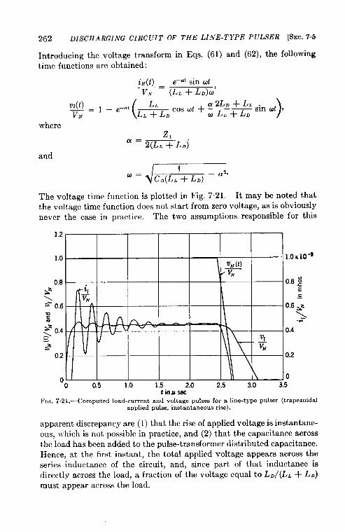
262 DISCHARGING CIRCUIT OF THE LINE-TYPE PULSER [SEC. 7.5
Introducing the voltage transform in Eqs. (61) and (62), the followingtime functions are obtained:
i~(t) _ e–~~sin CJ—_v. (L. + L.)(.O’
m(o _ ~ _ e–at(
L.
)
a 2LD + LL sin ~t ,
3z– L. + L.Cos d + –
OJL~+LD
wherez,
a = 2(LL + L.)
and
dm = C.(L.’+ L.)— az.
The voltage time function is plotted in Fig. 721. It may be noted thatthe voltage time function does not start from zero voltage, as is obviouslynever the case in practice. The two assumptions responsible for this
I\+. I I I I II I I .s
n I HI o“o 0.5 1.0 1.5 2.0 2.5 3.0 3.5
tin flwcFIG. 7.21.—Computed load-current and voltage pulses for a line-type pulser (trapezoidal
applied pulse, instantaneous rise).
apparent discrepancyy are (1) that the rise of applied voltage is instantane-ous, which is not possible in practice, and (2) that the capacitance acrossthe load has been added to the pulse-transformer distributed capacitance.Hence, at the first instant, the total applied voltage appears across theseries inductance of the circuit, and, since part of that inductance isdirectly across the load, a fraction of the voltage equal to LD/(IJL + L.)must appear across the load.

Sl!c. 7.5] COMPUTED AND ACTUAL PULSE SHAPES 263
This analysis is carried on until, by successive approximations, atime tlis found such that
Ut(tl) v.—. —.v, v.
The current through the circuit and the voltage across the condenser CDat that time are then computed. For the particular values of parameterschosen above, tl= 0.087 psec, IL,/VN = 416 X 10–6 mhos, and
Vc,E = 0.383.
The general form of the time function for the top of the pulse is toocomplex to permit a useful analysis of the effect of individual parameters,even with an applied voltage of the simple form assumed here. For theparticular values chosen for the parameters, the load’ voltage is of the form
in which the first term has the value
~zl+nA.= ‘;, +,1 = 0.452,
which is the steady-state value of the voltage arrived at from other con-siderations in Sec. 7.2.
The term Bud’ is an exponential with a very rapid decay, correspond-ing to the increase from starting to operating voltage. Again, for thisexample, B. = – 0.0048, and b = – 14.5 for texpressed in microseconds.The last term corresponds to the oscillations on the top of the pulse,for which C? = –0.416, c = – 2.24 for t expressed in microseconds,WI = 27.35, and O = 1.431. The time function for the current ia of thesame form as that for the voltage; the coefficients are given by
and
and the exponents, frequency, and phase angle are the same.

264 DISCHARGING CIRCUIT OF THE LINE-TYPE PULSER [SEC. 7.5
A plot of the load-voltage time function obtained with the aboveassumptions is given in Fig. 721. The amplitude of oscillations is muchgreater than that observed in practice because of the shock excitation ofthe pulse-transformer circuit. This excitation is introduced partly bythe discontinuous function chosen for the applied voltage, and partlyby the assumption that the switch voltage drops instantaneously to itsoperating value.
When the applied voltage begins to decrease at t = 2.5 psec, its timefunction is given by
()f
UN(t)=~N l—:,
with t’ = O at t= 2.5 ~sec, where t’is expressed in microseconds anda = 0.25 psec. The Laplace transform for the voltage
(:-3)’introduced in Eqs. (63) and (65) leads to a time function containing termsof the same form as those for o.df) = VN, Plus a term that is directlyproportional to the time. For the particular example chosen, the oscil-latory term is negligible, and the expressions for the load voltage andcurrent can be written
and
u(t)— – 0.475 – 0.308t – 0.023e–lA.52tv. –
106 ~ = 687 – 3077t – 230e–1452~ mhos.
The expression for m(t) is used until t = tz,tzhaving been defined as thetime for which
V1= R,.
z
The load static impedance at any instant is given by
Equating this value to R., the load voltage is determined as a function ofload parameters, that is
Vl(t,) = v, #-1’

SEC. 7.5] COMPUTED AND ACTUAL PULSE SHAPES 265
The time hat which this voltage is reached can now be obtained from thetime function for vI. In the present example, it is 2.71 psec. This valueis used in turn to determine the initial currents to be introduced in thecircuit from which the trailing edge of the pulse is computed.
The amplitude of oscillations on the top of the current pulse is deter-mined to a large extent by the energy stored in the charging inductanceof the pulse transformer, and their frequency is determined almostentirely by the distributed capacitance and charging inductance of thepulse transformer.
Since the applied voltage vw(t) is considered equal to zero for t > h,the initial conditions fo? the trailing edge of the pulse can readily befound as follows:
~_VN v~Le (t2 – h) = ~00~~o_3 X 2.62 X 10-’= 24 X 10-’ mhos,
v.,VNL— = 0.408,
and
The values for L. and C. are found to be
~, = 2..5 x 1O–’
2400= 1000 X 10–12farads,
andL. = Z;CN = 1.4 X 10⁻³ henrys.
If these values are introduced in the Laplace-transform equation for thiscircuit (Eq. (65)), the time function for the voltage across R. is found tobe
zu(t)t>t, _— – –0.178e-0022° sin (0, 134t – O.132)v.
–0.386e-0.3g4’ sin (3.52t – 1.49).
As can be seen from Fig. 7.22, the load voltage during the tail of the pulseconsists essentially of two damped sine waves, one of relatively highamplitude, frequency, and damping that corresponds approximately tothe LNCD-circuit, and one of lower amplitude, frequent y, and dampingthat corresponds very nearly to the L.CiwCirCUit.
The voltage buildup on the network capacitance CN is given by theexpression
vN(t)t>t,— = –0.182e-0.022’$ sin (0.134t – 0.121)VN
+0.022e-o.”a sin (3.52i! + 1.434),

266 DISCHARGING CIRCUIT OF THE LINE-TYPE PULSER [SEC. 7.5
and is also plotted en Fig. 7.22. If the switch is unidirectional, the net-work voltage V~ reaches a maximum negative value, at which time thedischarging circuit is disconnected from the network, and only the charg-ing circuit needs to be considered.
0.6
0.4 >
3v’
L2 0.2\>2
go Am~z
lb
---
+ ~ –
-- -- - —-->0.2 v z
0.40 5 10 15 20
tinusec
FIG. 7.22.—Computed voltage pulse on the load and backswing voltage on the load andon the pulse-forming network (trapezoidal applied pulse, instantaneous rise).
1.2 1.2X 10³
1.0
II
1.0%(t)~
<0.8 0.8
*- 8= ~1
[TNt
m 0.6~z I
\
0.6 .~
b~z
~ — — \
$0.4 /
b “B
0.4 “-
VN
0.2
0 /0 0.5 1.0 1.5 2.0 2.5 3.0
t in Asec
FIG.7,23.—Computed load-current and load-voltage pulses for a line-type pulser (trap-.zoidal applied voltage, finite time of rise).
One assumption that is implicit in the above discussion is that thecharging circuit has no effect on the shape or on the trailing edge of thepulse. This assumption is correct only if the charging inductance is
●

SEC. 7.5] COMPUTED AND ACTUAL PULSE SHAPES 267
very large compared with the shunt inductance of the pulse transformer.The effect may become appreciable if the ratio ~~ is less than 10.
Figure 7.23 shows the voltage and current pulse shapes obtained forthe same circuit conditions as those applying to the preceding discussion,but with an applied pulse shape that has a finite time of rise. Thedetailed analysis is not repeated, but it is worthy of note that the ampli-tude of the oscillations on the top of the pulse is reduced by a factor of atleast two by the decrease in the shock excitation in the circuit, as is tobe expected. In actual practice, the amplitude should be reduced evenmore because, as explained later, the switch-resistance characteristicsin a line-type pulser tend to decrease the rate of rise of the pulse on theload even though a unit step function of voltage is applied to the circuit.
0,4~ I I I I I 10 5 10 15 20
tin fisec
FIG. 7.24.—Computed voltage pulse on the load and backswing voltage on the load andon the pul-forrning network (trapezoidal applied voltage, finite time of rice).
The similarity between Fig. 7“24 and Fig. 7“22, showing the load voltageduring and immediately after the pulse, and the voltage on the networkcapacitance, is quite obvious. The principal difference between the twocases is a phase shift of the post-pulse oscillations corresponding approxi-mately to the time of build-up of the front edge of the pulse.
The series of oscillograms shown in Fig. 7.25 have been obtained witha circuit simulating a line-type pulser in order to indicate the effects ofdistributed capacitance and pulse-tranformer inductances on the topof the pulse. It may be noted that the damping of the oscillations isfaster than that predicted by theory as a result of the losses in the simu-lating circuit, which were neglected when making computations. It ishighly probable, however, that the losses in the actual circuit are evenhigher than those obtained by the use of air-core inductances and micricondensers. The frequency of the oscillations on the top of the puke is
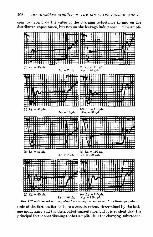
268 DISCHARGING CIRCUIT OF THE LINE-TYPE PULSER [SEC. 7.5
seen to depend on the value of the charging inductance Ld and on thedistributed capacitance, but not on the leakage inductance. The ampli-
(a) LL = 45 ~h. (fJ) LL = 110 ph.Lll = 7 ph. CD= 90 #if.
(c) LL = 45@. (d) L. = llo,uh.LD = 16Mh, CD= 90 PPf.
(e) LL = 45 ph. (j) L. = 11OJLLLD = 7 ph. CD = 150 ~Llf.
(g) LL = 45 ph. (h) ~L = 110 ~h.LD = 16 ph. CD= 150 PPf.
Fm. 7.25.—Observed output pulsee from an equivalent circuit for a line-type pulser.
tude of the first oscillation is, to a certain extent, determined by the leak-age inductance and the distributed capacitance, but it is evident that theprincipal factor contributing to that amplitude is the charging inductance.

SEC.7.5] cOMPUTED AND ACTUAL PULSE SHAPES 269
A comparison of these photographs with those shown in Fig. 7.30indicates that the amplitude of the oscillations obtained in an actualpulser circuit and with a magnetron load is less than that to be expectedfrom theoretical considerations. The circuit constants used for the abovecomputations and photographs are very nearly equal to those obtainingfor Fig. 7.30. The simplifying assumptions, such as the lumping ofcapacitances and inductances to obtain a workable circuit, account forthis difference.
Eflect oj the Switch Resistance. —During the foregoing discussion thes\vitch resistance is assumed constant in order to simplify the equations,although it is a function of time for the start of the pulse. A very simpleexample is treated here to show the effect of the switch resistance on thefront edge of the voltage pulse on a resistance load. Figure 726 repre-
FIG.7.26.—Equivalent discharging circuitfor study of the effect of switch resistance.
~o a t-
FIe-. 7.27.—Assumed switch-resistance char-acteristics.
sents the discharging circuit and Fig. 7“27 gives the assumed switch-resistance characteristics.
Two assumptions are made concerning the variation of switch resist-ance as a function of time (discussed in Chap. 8):
1. That the resistance decreases linearly from a value RPO at thebeginning of the pulse to a value R,a at a time t = a, and is equalto Rp. for the remainder of the pulse.
2. That the decrease in resistance from the same value R=O to thevalue R=a at t = a is parabolic.
This latter method avoids any discontinuity if the vertex of the parabolais at point A and if its axis is parallel to the resistance axis. For a lineardrop in resistance, the switch resistance from the time t = O to the timet = a is expressed as
Rp – RpoTp=Rpo+ ~
()t= Rp. +( Rpo– RJ 1–:1
and the voltage across the load resistance RI is then given by
V,v(t)&
‘~(~) = Z~ + RI + rpfor O<t <a,

270 DISCHARGING CIRCUIT OF THE LINE-TYPE PULSER [SEC. 7-5
orw(t) RlVN(t) =
()ZN+Rl+R.. +( RpO– Rp.) ~_j”
a
Assuming that v~(t) = O for t <0, that u~(t) = V~ for t >0, and thatZ~ = Rl, R,O = 2R,, R,a = 0.05 Rl, and a = 0.25 psec, the time functionof the load voltage may be simplified to
Vi(t) = 1v.. 4 – 7.8t
for O < t < a, where t is expressed in microseconds. For t > a,
?)I(t) R1 _ 1n= Z,v + Ri + R,. = 2.05
for the values chosen.Assuming a parabolic decrease in resistance, the expression for resist-
ance becomes
()TP=(RPO– RW) 1–:2+RW for (O < t < a),
and the load voltage becomes
Vi(t) RI%=
()
2“
ZN+RI+Rpa+(Rpo– RpJ 1–:
Again, for t > a,Vi(t) Rl
T= Z.v + Rl + R..”
With the values of constants assumed for a linearly varying resistance,
05
‘m
the expression for the voltage across the load.-resistance becomes
0.4v~(t ) 1
i“03—.v. 4 – 15.6t + 31.2tz”
~:~02 The effect of a variable switch resistance
0.1 is shown in Fig. 7.28. This effect is seen tobe essentially the same as that obtained from
00 0.1 02 03 0.4 0.5 a time function v.~(t), with a time of rise1mu sec
FIG. 7.2S.—C o m p ut e dlonger than the actual one, and a constant
effect of a variable switch switch resistance R=a. Hence, the method of.~~i~tanoeon the front edge,.,f the voltage pulse for a
approach described earlier in this section canI-si~tanCe]Oad~n~arectang”. be used with reasonable accuracy, if the~w applied pulse. proper assumptions are made concerning thetime of rise of the applied voltage v~(t).

SEC. 7.5] COMPUTED AND ACTUAL PULSE SHAPES 271
Eflect oj Pulse Cable between” Pulser and Load. -If a pulse cable isinserted between the pulser and the pulse transformer, its effect on thepulse shape does not lend itself to easy mathematical treatment for theloads encountered in practice. In general, it can be said that, if the loadis a biased diode, the shapes of the top of the current pulse and the trail-ing edge of the voltage pulse are affected by changes in the length of acable between pulser and load. Oscillograms of 0.2-psec voltage andcurrent pulses obtained with a 4J52-.magnetron load using 6 and 50
(a) 6 ft of cable, fact sweep. (b) 50 ft of cable, fast sweep.
(c) 6 ft of cable, slow sweep. (d) 50 ft of cable, elow sweep.
Fm. 7.29.—OsciUograms showing the effect of cable length on the pulse shapes for0.2-psec current puke.
a
ft of cable are shown in Fig. 7“29. S1OWand fast sweeps were used toshow both the top of the current pulse and the trailing edge of the voltagepulse; sweep calibrations of 5 and 1 Me/see respectively are also shown.Two facts are immediately obvious: (1) in this particular case, the currentamplitude tends to decrease as a function of time if a short cable is used,and to increase if a long cable is used, and (2) high-amplitude oscillationsare present on the trailing edge of the voltage pulse when the long cableis used.
Not enough information is available at present to evaluate exactlythe causes for the changes introduced in the pulse shape by the cable;the problem-involves, in addition to the cable characteristics, the variety

272 DISCHARGING CIRCUIT OF THE LINE-TYPE PULSER [SEC. 7.5
of parameters considered previously in this section. These characteris-tics include impedance, attenuation, and phase shift, which may vary as afunction of frequency. Thus, individual cases lead to entirely differentresults.
Another example is shown in Fig. 7.30, where voltage and currentpulse shapes on a 4J52 magnetron are shown for a 2.4-psec pulse. Inthis case, additional oscillations appear in the current pulse when a longcable is used. After the first 0.7 psec, these oscillations take the shape of
(a) 6 ft of cable, fast sweep. (b) 50 ft of cable, fast sweep.
(c) 6 ft of cable, slow sweep. (d) 50 ft of cable, slow sweep.FIG. 7.30. —Oscillograms showing the effect of cable length on the pulse shapes for a
2.4-psec current pulse.
a distorted damped rectangular wave superimposed on the current pulse.Graphical subtraction of the two current pulses leads to the conclusionthat this distortion is the result of a highly damped sine-wave oscillationsuperimposed on a slightly damped rectangular wave. The half periodof this distorted rectangular wave is slightly longer than the two-waytransit time in the cable; the difference can almost entirely be accountedfor by the time delay in the pulse transformer. The amplitude of oscilla-tions on the trailing edge of the voltage pulse is essentially the same forboth long and short cables; the period, however, is slightly increased bythe addition of ~ long cable.

CHAPTER 8
SWITCHES FOR LINE-TYPE PULSERS
BY J. V. LERACQZ,H. J. WHITE, J. R. DILLINGER, A. S. JERREMS,ANDK. J. GERMESRAUSEN
Some of the requirements for switches that can be used to initiate thedischarge of the pulse-forming network have already been mentioned inChap. 1. Briefly, these requirements may be summarized as follows:
1. The switch should be nonconducting during the charging period.2. The switch should be capable of closing very rapidly at predeter-
mined times.3. The switch resistance should be as small as possible during the
discharge of the network.4. The switch is not required to interrupt the pulse current, since the
current drops to zero or nearly to zero at the end of the pulse.5. The switch should regain its nonconducting state rapidly after
the end of the pulse.
The requirements of low resistance and rapid closing of the switchsuggest that either spark gaps or gaseous-discharge tubes should be usedas switches in line-type pulsers. The problem of closing the switch orinitiating the discharge at predetermined times has beeq a serious onebecause, for some applications, an accuracy of about 0.02 psec is desired.Both thyratrons and triggered spark gaps have been developed to meetthis exacting requirement successfully. Rapid deionization of the gasafter the discharge is essential if high recurrence frequencies are required.Since the nature and pressure of the gas, the electrode geometry, the totalionization produced by the pulse current, and the type of charging cir-cuit used all affect the deionization time, some compromise may haveto be reached between the pulse power and the maximum recurrencefrequency, independent of the safe allowable average power. In sparkgaps electrode erosion occurs, changing the gap geometry and the break-down characteristics. Attention must also be given to the residual gasesproduced by the spark under certain conditions.
Since rotary spark gaps had been used successfully in radio code trans-mitters, they were suggested for use in radar pulsers, and proved verysatisfactory. They presented three main disadvantages, however: (1)
273

274 SWITCHES FOR LINE-TYPE PULSERS
they are not well suited for high recurrence frequencies, (2) they have aninherent uncertainty in the time of firing, which may be as high as 50 ysec,and (3) they cannot readily be adapted to applications requiring air-tight enclosures. As a result, developmental work was started on bothfixed spark gaps and thyratrons. The early investigations covered suchpossibilities as veatrons (vacuum arc devices)a nd ignitrons, 1fixed two- andthree-electrode gaps operating in air with a forced circulation of the airin order to aid deionization, 2 and mechanical switches operating in avacuum. 3 The ‘ %rigatron, ”4 an enclosed three-electrode gap was foundto be satisfactory for lowpower applications in which long life was notrequired. Some work was done on an enclosed three-electrode gap forapplications requiring high power and long life. s Of all these devices,an enclosed fixed gap having two electrodes and operated in series withone or two similar gaps showed the greatest promise of early satisfactorydevelopment, and the effort was therefore concentrated on these so-called“series gaps. ”e
A series-gap switch is preferable to the rotary spark gap for thefollowing reasons: (1) the time fluctuations in the initiation of the dis-charge are smaller (1 to 2 ~sec for one type of series gap, O.O2 ~sec foranother type), (2) it can easily be operated at more than one pulse recur-rence frequency in a given installation, (3) it can be operated at recurrencefrequencies that are higher than those conveniently obtained with arotary gap, and (4) each fixed spark gap is completely enclosed.
Early work on existing mercury thyratrons’ indicated the desirabilityof developing a switch that would eliminate the variation of character-istics as a function of ambient temperature, and that would use a gas I
that would not damage the cathode when passing the high peak currentsrequired. A@ much experimentation, the hydrogen thyratron was ‘developed at the Radiation Laboratory, and proved to be the most satis-
I C. M. Slack, “Report on PulserTube Development,” NDRC 14105, Westing-house Electric Corporation, May 15, 1942.
2L. Tonks (General Electric Company), “Fixed Spark Gaps and Associated Cir-cuits,” Spark Gap ColLogUiU~, RL Report No. 50-1, Sept. 28, 1942.
R. G. Fluharty, “Life Test Report on TriggeredSpark Gaps Developed by L.Tonks at the G. E. Company,” RL InternalReport 51-Apr. 7, 1943.
~J. V. Lebacqz, H. O. Anger,and T. W. Jarmie, ‘‘ MechanicalVacuum Switches,TransmissionLineand RC PulsingCircuits,” NDRC 14-156,U. of Calif., June1, 1943.
f J. D. Craggs, M. E. Haine, and J. M. Meek, “The Development of TriggeredGaps with Particular Reference to Sealed Gaps,” Metropolitan-Vickers ElectricCo., Ltd., Report No. C-31 1, September 1942.
‘ C. M. Slack, and E. G. F. Arnott, “Report on Enclosed Pressure Gaps, ” NDRC14-150, Westinghouse Electric Corporation, Dec. 31, 1942.
6 F. S. Goucher, J. R. Haynes, W. A. Depp, and E. J. Ryder, ‘‘ Spark Gap Switchesfor Radar,” Bell Sysfem Technicul Journal, Oct. 1946.
TA. W. Hull (General Electric Company), “ Mercury Vapor Thyratron, ” il40du-lator CoUoguium, RL Report No. 50-2, June 9, 1943,pp. 11S-120.
i

SWITCHES FOR LINE-TYPE PULSERS 275
factory switch throughout the power range which it covers. With thisswitch, the time fluctuation can easily be kept to 0.02 ysec or less, and theauxiliary circuits required for the trigger puke are very simple comparedwith those necessary to supply a high-voltage trigger pulse to the series-gap switch.
The characteristics, uses, and special requirements of rotary sparkgaps, enclosed fixed spark gaps, and hydrogen thyratrons in pulsercircuits are considered in this chapter.
THE ROTARY SPARK GAP
BY J. V. LEBACQZ AND H. J. WHITE
A very brief discussion of the sparking mechanism at or near atmos-pheric pressure may be helpful in understanding the limitations andadvantages of the different kinds of rotary spark gaps. A spark may bedefined, for the purpose of the present discussion, as the transient,unstable breakdown of a gas between electrodes whereby the gas issuddenly changed from a good insulator to a relatively good conductor.It results from the formation of a highly ionized path between twoelectrodes, and, within the limits of voltages considered here, the finalvoltage-current characteristics of the spark usually depend more on theexternal circuit than on the gap dimensions.
A spark is initiated between two electrodes by raising the voltage to,or above, the static-breakdown voltage. The static-breakdown voltageis the minimum voltage that, if applied to a given gap for a long enoughtime, eventually causes it to break down. The concept of time is intro-duced here because the breakdown is initiated by the ionization of thegas molecules by free electrons accelerated in a strong electric field.Under favorable conditions, the process is cumulative and breakdownresults; however, the time lag, or the time elapsed between the applica-tion of the static-breakdown voltage and the initiation of the discharge,may be as long as several minutes. If a voltage higher thah the static-breakdowh voltage is applied, or if a large number of electrons are madeavailable in the gap, the chances of obtaining conditions favorable toionization increase and the statistical time lag decreases. In general,if the voltage applied to the gap is two to three times the static-breakdownvoltage, and if some initial ionization is provided, the time lag of the gapcan be reduced to 10–9 to 10–7 seconds.
Once the ionization process has been initiated, some time still elapsesbefore the breakdowm takes on the character of a spark, This time isreferred to as the “breakdown time” of the gap and depends on its geom-etry and on the pressure and nature of the gas, as well as on the shape ofthe applied voltage wave. Observations indicate that the breakdown
I
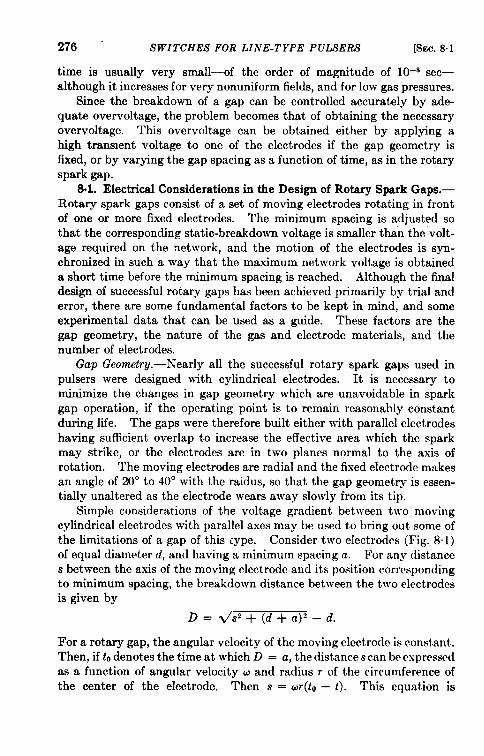
276 SWITCHES FOR LINE-TYPE PULSERS [SEC. 8.1
time is usually very small—of the order of magnitude of 10–6 sec—although it increases for very nonuniform fields, and for low gas pressures.
Since the breakdown of a gap can be controlled accurately by ade-quate overvoltage, the problem becomes that of obtaining the necessaryovervoltage. This overvoltage can be obtained either by applying ahigh transient voltage to one of the electrodes if the gap geometry isfixed, or by varying the gap spacing as a function of time, as in the rotaryspark gap.
8.1. Electrical Considerations in the Design of Rotary Spark Gaps.—Rotary spark gaps consist of a set of moving electrodes rotating in frontof one or more fixed electrodes. The minimum spacing is adjusted sothat the corresponding static-breakdown voltage is smaller than the volt-age required on the network, and the motion of the electrodes is syn-chronized in such a way that the maximum network voltage is obtaineda short time before the minimum spacing is reached. Although the finaldesign of successful rotary gaps has been achieved primarily by trial anderror, there are some fundamental factors to be kept in mind, and someexperimental data that can be used as a guide. These factors are thegap geometry, the nature of the gas and electrode materials, and thenumber of electrodes.
Gap Geometry.—Nearly all the successful rotary spark gaps used inpulsers were designed with cylindrical electrodes. It is necessary tominimize the changes in gap geometry which are unavoidable in sparkgap operation, if the operating point is to remain reasonably constantduring life. The gaps were therefore built either with parallel electrodeshaving sufficient overlap to increase the effective area which the sparkmay strike, or the electrodes are in two planes normal to the axis ofrotation. The moving electrodes are radial and the fixed electrode makesan angle of 20° to 40° with the raidus, so that the gap geometry is essen-tially unaltered as the electrode wears away slowly from its tip.
Simple considerations of the voltage gradient between two movingcylindrical electrodes with parallel axes may be used to bring out some ofthe limitations of a gap of this type. Consider two electrodes (Fig. 81)of equal diameter d, and having a minimum spacing a. For any distances between the axis of the moving electrode and its position correspondingto minimum spacing, the breakdown distance between the two electrodesis given by
D=~s2+(d+a)2–d.
For a rotary gap, the angular velocity of the moving electrode is constant.Then, if todenotes the time at which D = a, the distances can be expressedas a function of angular velocity u and radius r of the circumference ofthe center of the electrode. Then s = CM-(tO– t). This equation is

fi?,c.8.1] ELECTRICAL DESIGN OF ROTARY SPARK GAPS 277
correct only to the same approximation that u(to – t) ==sin u(to – t);forusual rotary-gap practice, theangle over which thespark may takeplace isalways so small that theerror introduced is negligible. Hence,the average voltage gradient between electrodes can be expressed as
~=~= v. v.
D tis’+(d+a)’-(i= Uu’r’(to – t)’ + (d+ a)’ – d’
where V~ is the network voltage. For reasons explained later, resonantcharging is nearly always used for rotary-gap pulsers. In this case, thenetwork voltage is so nearly constant near the discharge point that itmay be assumed constant without introducing appreciable error. Anexact discussion of the sparking phenomena requires a knowledge of themaximum electric field between elec-trodes for every position of the moving
200
electrode. In the following discus-sion it is assumed that the voltagegradient E is uniform between the <electrodes. It is also assumed that a z ~wspark may occur at any time after the ~electric field exceeds 30 kv/cm, and ~occurs instantaneously if the electricfield reaches a value of 70 kv/cm.These assumptions are obviously far ofrom correct, and are not intended togive a quantitative solution to the s m cm
Movingproblem of gap design. If made con- ~ ~ i electrode
Psistently for various conditions, how- * : s + Directionever, they do lead to results that are of motion
in accord with experience, and are a ‘Q
therefore sufficiently accurate to in- ‘d’dicate the expected trends of the phe- ‘
Fixed electrode
nomena. For instance, it is shownlater that the experimental average
FIG. S.1.—Average field betweenrotary-gap electrodes. Curve A is for
gradient before static breakdown for VN = 10 kv. a = o.os Cm CurveB is
a gfven gap varies as a function offor VN = 10 kv, a = 0.10 cm, andcurve C is for V,v = 20 kv, a = 0.10 cm.
spacing, and is higher than 30 kv/cmat the smaller spacings. The introduction of this variation in the mini-mum average gradient in the discussion at this point would result inmany additional complications without altering the conclusions.
For any given vaIues of applied voltage, electrode dimensions andminimum spacing; and velocity of the moving electrode, a time t = tl canbe found at which the voltage gradient reaches 30 kv/cm. Similarly, atime t = tz may be defined as the time at which E = 70 kv/cm. The

278 S WITCHES FOR LINE-TYPE P ULSERS [SEC. 81
spark then occurs between tl and tz. Thus, (b — tJ corresponds tothe maximum time jitter that may be expected because of uncertain y inthe initiation of the gap discharge. As an example, consider the hypothet-ical gap of Fig. 8.1, and assume that the electrodes are 0.25 cm in diameter.The average gradient has been plotted as a function of s for several valuesof V. and a. Then, with the assumptions made above, a spark may takeplace at any point between s = 0.25 and s = 0.5 cm for curve A; betweens = 0.18 ands = 0.43 cm for curve 1?; and betweens = 0.41 ands = 0.85cm for curve C. To express these results as a function of time, someelectrode velocity must be assumed. Taking r = 10 cm and a rotorspeed of 60 revolutions per second, the linear velocity of the movingelectrode is
Or = 27r X 60 X 10 = 3750 cm/sec
Then, the maximum time jitter can be estimated as 0.25/3750 sec or65 ~sec for curves A and B, and about 115 psec for curve C.
These values are larger than those normally found in practice (1)because of the crudeness of the assumptions concerning field distributionand breakdown voltages, (2) because the time lag at minimum breakcfowmvoltage has been considered equal to zero, and (3) because the possibilityof the formation of corona has been neglected. Actually, for the gapgeometry considered, the minimum value of the average static gradient atbreakdown is probably nearer 40 than 30 kv/cm. If this value is chosen,and if the gap is assumed to break down with a time lag smaller than 1psec when the voltage is equal to 150 per cent of the minimum breakdownvoltage, 60 kv/cm in this case, the values obtained for inherent timejitter in the gap are 30 psec for curves A and i? and about 50 ~sec forcurve C. >Tevertheless, the results can be used either to compare thebehavior of gaps having different geometries, that is, where the ratio ofthe minimum spacing to the electrode diameter varies, or to compare theoperation of gaps with similar geometries at different voltages.
The time jitter to be expected is inversely proportional to the relativespeed of the electrodes. Thus, in order to decrease the inherent timejitter caused by the statistical nature of the sparking process, it istheoretically sufficient to increase the steepness of the curve sho}vingthe variation of field with spacings or time within the range of \roltagegradients that is most apt to produce a spark. One method of achievingthe desired result is to increase the speed of the moving electrode. Ajudicious choice of electrode diameter and spacing for a gil-en operatingvoltage is also necessary. For instance, referring to Fig, 81 and theprevious discussion, it is seen that the time jitter of the gap \vith aminimum spacing of 0,10 cm for an applied voltage of 20 kv is almostt!vice its value for an applied voltage of 10 kv,

SEC. 8.1] ELECTRICAL DESIGN OF ROTARY SPARK GAPS 279
If the moving-electrode velocity is held constant, the inherent timejitter of a gap that has an electrode diameter and minimum spacing thatare twice those of the gap considered in the previous example and thatoperates at 20 kv is still much greater than that of the gap operating at10 kv. Since the mechanical design imposes a limit on the maximumelectrode velocity, it is advantageous, in some cases, to use two gaps inseries if the total vo)tage becomes very great. This method has beenused in some rotary gaps designed at the Radiation Laboratory.
If the voltage across a rotary gap is increased gradually, the gapbegins to break down erratically when the field corresponding to theminimum spacing reaches the critical gradient at which the spark mayoccur with a long time lag. If the voltage is further increased, the gapbegins to break down on every pulse, and usually reaches a point of opti-mum operation. If the voltage is increased still further, the length ofthe gap at which the spark jumps increases, as well as the time jitter.
Another very important consideration in gap design is that of deioniza-tion. As pointed out previously, the gap is not required to interrupt themain pulse current. The network, however, starts to recharge immedi-ately after the pulse, and care must be taken that its voltage does notexceed the breakdown voltage of the gap at any time before the end ofthe desired interpulse interval. Since the air in the vicinity of theelectrodes is highly ionized by the passage of the spark current, it is safeto assume that there is very little time lag before breakdown, even forthe minimum voltage gradient. If losses are neglected and the networkis assumed to discharge completely, the voltage across the gap may beexpressed as
UN= ; (1 – Cos cod)
for d-c resonant charging, and the average field is
where D is defined as before. As an example, consider the gap of Fig. 8.1curve A with V~ = 10 kv, and assume that the spark has taken placewhen E = 40 kv/cm. If the pulse recurrence frequency is 600 pps,
1). = 5(1 – COS600 rt),
and the electrode velocity is 3750 cm/sec. Thus, the voltage gradientacross the gap can readily be plotted as in Fig. 8.2 for various positions ofthe moving electrode. For the particular values of parameters chosen,there is no danger of the gap restriking and establishing a short-circuiting.arc across the power supply. If the same gap were used at VM = 20 kv,

280 SWITCHES FOR LINE-TYPE PULSERS [SEC. 8.1
however, the network discharge might take place at s = 0.7 cm. Then,the voltage built up on the network at the time of minimum spacingbetween the electrodes would be about 610 volts, corresponding to anaverage gradient greater than 12 kv/cm. Because of the nonuniformityof the field, which can be caused by rough electrodes resulting from long
8 in cm
-- Direction of motion
FIG. S.2.—Average field betweenelectrodes during the beginning of acharging cycle for d = 0,25 cm, a = 0.05cm, f, = 600 PPS, wr = 3750 cm/see,where d, a and s are shown in Fig. 8.1.
kv/cm if the gap did not break
operation, the gap may be expectedto restrike under these conditions.The average voltage gradient as afunction of pin spacing has beenplotted for this case in Fig. 8.2.
In conclusion, some practical re-sults are given. Experience has shownthat high-power gaps work satisfac-torily with an average gradient be-tween 60 and 70 kv/cm correspondingto minimum spacing (Fig. 8“1), andthat low-power gaps may be builtand operated with minimum spac-ings that would correspond to aver-age gradients of between 200 and 300
down before that point were reached.These figures are only indicative of the range that has been used, andeach case has to be considered separately, depending on the requiredrecurrence frequency, the time jitter, the type of charging circuit, andthe type of load.
Gas and Electrode Material.-According to the most widely acceptedtheories, gap breakdowm takes place exclusively in the gas and is inde-pendent of the material used for electrodes, except inasmuch as it maycontribute to the initial ionization of the gas, either by radioactivity y or byphotoelectricity. Thus, the choice of electrode material is determined byother considerations, such as the necessity of obtaining a long trouble-free operating life. Since high temperatures are developed in high-cur-rent sparks, refractory material should be used for the electrodes, andconsequently tungsten was chosen for the initial tests on rotary sparkgaps. Because of the satisfactory operation of these gaps, tungstenelectrodes were used in nearly all the rotary gaps designed at the Radia-tion Laboratory. The original gaps were designed to operate in air atatmospheric pressure, where a breakdown field of 30 to 50 kv/cm,depending on the spacing, is applied. Tests on sealed rotary gaps, aswell as on fixed spark gaps, indicated that the presence of oxygen wasnecessary to obtain a satisfactory life from the tungsten electrodes. Theexact reason is not known, but it is believed that the formation of alayer of tungsten oxide provides a protective covering for the gap spark-

SEC. 8.1] ELECTRICAL DESIGN OF ROTARY SPARK GAPS 281
ing surfaces that greatly reduces the electrode wear. Ventilated rotarygaps using tungsten electrodes have been used in the great majority ofradar applications, although they cannot be used in airborne radar setsbecause of the change in breakdown voltage with pressure. Sealed rotarygaps have been used in one airborne radar. set, for which the life require-ments are much less severe than for ground-based or shipborne sets.
A number of life tests on rotary gaps have been made both at theRadiation Laboratory and at the Bell Telephone Laboratories. Theresults are all in reasonable agreement, and show that the rate of cathodewear is much larger than that of anode wear. Since the electrode wearappears to be approximately proportional to the total charge passed by thegap, a logical unit for rate of wear is the loss of mass per unit charge. Inpractice, a convenient unit for rate of wear is milligrams per ampere-hour.Experimental data obtained both at the Bell Telephone Laboratoriesand the Radiation Laboratory show that, for pulse currents from 40to 170 amp, the rate of cathode wear in air varies between about 2 and6 mg/amp-hour, 3 or 4 mg/amp-hour being the median value. In nitro-gen or gas mixtures that do not contain oxygen, the rate of wear is 10to 20 times greater. The order of magnitude of the rate of anode wearin air is only ~ that of the cathode.
0.5
0.4
)
0.3
0.2 / ‘
(0.1 /
8() 00
00 0.100 0.200
Electrode diameter in inches Electrode diameter in inches
FIG. S.3.—Diameter of the moving electrode for satisfactory gap operation and life.
Figures 83 and 8.4 show the relationship between pulse power and
average current and the diameters of the moving and fixed electrodes,
obtained from gap designs that have given satisfactory operating life.
ln these gaps, the fixed electrode is the anode and, as there are always
several moving electrodes, the wear is divided between them. The
values indicated b.y the curves can be regarded as the maximum safe
operating power and current for any given electrode diameter, asmined from present experience, that allows a satisfactory gap life.
deter-

282 SWITCHES FOR LINE-TYPE PULSERS [8Ec. 8.1
Number of Electrodes.—The number of fixed and rotary electrodes,Nf and N,, is related to the angular velocity, W,of the rotor (in revolutionsper second) and the required pulse recurrence frequency, j,, by therelation
f,= N,N#. .
This relation applies only if the respective positions of fixed and rotatingelectrodes are such that the minimum spacing between electrodes isnever reached simultaneously by more than one fixed and one rotatingelectrode. If, for instance, there are six rotor and six stator electrodes allspaced 60 mechanical degrees apart, the total number of sparks perrevolution is six, the same number that would be obtained for one, two,or three stator electrodes equally spaced. If, on the other hand, thereare five rotor and three stator electrodes equally spaced, the number ofsparks per revolution is 15, and f, = 15w
0 0.100 0.200 o 0.100 0,200Electrode diameter in inches Electrode diameter in inches
FIG. 8.4.—Diameter of the fixed electrode for satisfactory gap operation and life.
In general, because of the mechanical difficulties involved, only onefixed electrode is used, except for special applications such as the Marxcircuit (see Sec. 11.8) or the half-wave a-c charging circuit (see Sec.11.6). In these cases, it is necessary to obtain two or more sparks simul-taneously, and the number of fixed electrodes must therefore be at leastequal to the total number of discharge paths desired. It should also bepointed out that the formula gives the average recurrence frequencyfor one complete cycle, and does not specify the actual value of the recur-rence period. In general, it is desired to make all the interpulse intervalsequal, so the angle between rotating electrodes is constant and equal to27r/Nr for the usual case of one fixed electrode. The radius of the circleof rotating electrodes is determined by considerations of electrode veloc-ity necessary to minimize the time jitter and to prevent the restriking of

SEC. 8.2] MECHANICAL DESIGN OF ROTARY SPARK GAPS 283
the spark between electrodes during the charging period. It has beenfound that satisfactory operation can generally be maintained if thedistance in inches between consecutive electrodes is greater than onetenth the maximum network voltage expressed in kv. A factor ofbetween one sixth and one eighth is commonly used to provide a desirablefactor of safety,
Finally, the length and overlap of the electrodes should be considered.Although no general rules can be given, a few facts can be used as a guide.The -overlap should be large enough to allow a reasonable sparking areain order to prevent the gap geometry from being changed very rapidlyby the wearing away of the electrodes; on the other hand, it has beenfound that the time jitter increases if the overlap becomes excessive.The total length of the electrodes protruding from the rotor or the statorbushing must be sufficient to produce as little field distortion as practi-cable at the ends of the cylindrical electrodes. The values which havebeen used in the rotary gaps designed at the Radiation Laboratory aregiven in Table 8.1, and can be used as a guide in the design of gaps ofsimilar specifications.
From considerations of electrode wear, the rotating electrodes areusually made the cathode of the gap. With the pulser circuits mostcommonly used, it is therefore sufficient to ground the rotor to completethe pulser dk.charging circuit. Possibly the simplest way of accomplish-ing this grounding is to use a solid metal rotor and let the bearings carrythe current; however, because of the local sparking and electrolysis actionwhich takes place, the life of the bearings is considerably reduced ifcurrent is allowed to pass through them. Consequently, all rotors shouldbe built with an insulating disk between the shaft and the sparkingelectrodes. The pulse current can then be collected either by brushes,which are satisfactory for low voltages and low power, or by a sparkingsegment that is located very near the rotor.
8.2. Considerations of Mechanical Design.-The speed of rotation,the rotor diameter, the minimum electrode spacing, the number of elec-trodes, and their size and shape can be dethmined by considerations ofelectrical design. There still remains to be determined the rotor size,the motor power, the gap housing, and methods of mounting the elec-trodes. Actually, both mechanical and electrical design have to becarried out simultaneously, at least up to a certain point. For example,the rotor speed may have to be determined by the motor speeds avail-able, and the number of electrodes adjusted to obtain the required recur-rence frequency.
Size o.f Rotor.—The rotor disk must run true on the motor shaft, mustbe free from wobble, and must have a thickness sufficient to insure rigidityand to permit machining. Nickel-plated brass is commonly used as

284 SWITCHES FOR LINE-TYPE PULSERS [SEC.8.2
the rotor material, and the thickness varies from ~ to ~ in. The holesfor mounting the tungsten pins used as electrodes are either bored orground and tapered to insure an accurate fit. In order to obtain smoothsatisfactory operation of a rotary gap, it is important to maintain thepositions of the rotary electrodes within the specified maximum toler-ances. A precision index head must be used for this purpose.
The importance of machining tolerances can readily be understoodfrom the following discussion. Let
be the average peripheral spacing between rotary electrodes, and assumethat Nf = 1. If one of the rotary electrodes is displaced by an amountAL along the circumference from the position it should occupy, so thatthe dist ante to adj scent pins is (L + AL) respectively, the correspondinginterpulse intervals are given by
T,– AT, =~(L– AL)
and
T,+ AT, =~(L+ AL),
if the effects of time lag in breakdown discussed in Sec. 8.1 are neglected.It is thus seen that, for a displacement AL in one electrode, the expectedtime jitter produced by mechanical inaccuracy is given by
AT, = ~ T,#
If a tolerance of 1is imposed on the peripheral location of the electrodes,the minimum and maximum spacings between consecutive electrodes mayvary from (L – 2J) to (L + 21) and the maximum time jitter that may beexpected from this cause alone is.
AT, = +T, ;.
Errors in the radial position of the electrodes have a similar effect,as can readily be understood from Fig. 8.1. If, for V~ = 10 kv, theminimum distance a is increased from 0.05 to 0.1 cm (about 0.02 to 0.04in., or a radial displacement of 0.02 in.), and the breakdown of the gap isassumed to take place without time lag for an average field of 40 kv/cm,the distance s at which breakdown takes place is decreased from 0.40to 0.33 cm. Hence, the effect on time jitter is the same as if the spacingbetween consecutive rotary electrodes varied by 0.07 cm. This particu-
SEC. 82] MECHANICAL DESIGN OF ROTARY SPARK GAPS 285
lar case must be considered as an exception, in that the radial tolerancein position leads, in general, to less time jitter than an equal peripheraltolerance, and not to more as indicated by this example.
The tolerances at the sparking point, which is usually near the tipof the electrode and not at the rotor disk, are the values to be controlled.13xpcrience at the Radiation Laboratory indicates that, for most satis-factory operation, these tolerances should not exceed O.OO5in. for periph-eral and 0.003 in. for radial alignment at that point. Assuming thatthe electrodes are 1 in. long and perfectly spaced on the rotor, they haveto be aligned with a deviation of less than 10 min of arc in order to satisfythe tolerance requirements.
The results of tests on a 7-pin rotary gap with an outside diameter of5.5 in. and rotating at 3450 rpm indicate the effect of machining inac-curacy on time jitter. The average peripheral spacing was about 2 in.,and the measured radial tolerance was f 0.002 in. For a maximum meas-ured variation in peripheral spacing of 0.036 in., the maximum theoreticaltime jitter from this cause alone would be 45 psec, and the observed timejitter \ras approximately 50 ~sec. When the variation in peripheralspacing was reduced to 0.010 in., the observed time jitter was reduced toapproximately 25 ~sec; a value of 13 psec would be expected from theerror in spacing alone. The figures for observed time jitter were obtainedunder conditions of network voltage corresponding to a minimum jitter.
Mofor and. Ifousing.—In all practical gaps designed at the RadiationLaboratory, the rotor is mcunted directly on the shaft of the drivingmotor; hence, the speed of the motor is easily determined. As hasbeen mentioned previously, a compromise usually has to be reachedbetiveen the number of electrodes and the speed of rotation. One ofthe factors limiting this speed is the life of the bearings: very fast motorsnormally tend to develop play in the bearings, \vhich adds to the toler-ances of the gap and may render it inoperative in a very short time.
Once the motor speed is determined, its power can be obtained byconsiderations of rotor inertia, ~vhich determines the required startingtorque, and its Ivindage and friction losses, Irhich determine the runningtorque. Because of the required rigidity, the shaft and bearings haveto be chosen as large as is practicable for the motor size required. InTable 8.1 the pertinent motor data for a large number of rotary gaps areIistcci, which can be used as a guide in design. All rotary gaps havebeen enclosed in a metal housing. The main purpose of the housing isto allow for self-ventilation of the gap and to prevent the corrosive vaporsformed by the spark from escaping into the cabinet containing the pulsercomponents. The nitric acid, which can be formed by combination ofthese vapors and water vapor in the air, must not be allowed to condenseon any vital part of the pulser. By enclosing the gap in a housing it is

286 SWITCHES FOR LINE-TYPE PULSE f&S [SEC. 8.2
also possible to reduce noise, to protect against accidental electrodebreakage, and to reduce the windage losses with a corresponding savingin motor size.
Housings have been made of pressed steel, cast iron, or cast aluminum.The cast housings are usually preferred for the higher powers, and areused almost exclusively for gaps in a-c charging pulsers. In this case,the housing is required to perform the additional function of phasing thegap breakdown with the applied-voltage wave shape. This phasing isusually accomplished by rotating with respect to the frame of the motorthe part of the housing that carries the high-voltage fixed electrode. Anynumber of screw and gear arrangements can be used to achieve this pur-pose, and the housing has to be machined in order to permit some rotation,the amount of which depends on the number of rotary electrodes. Insome cases, the phasing adjustment is motor-driven in order to permitremote control.
The self-ventilation of the rotor and pins is usually sufficient to pro-vide an air circulation of 1 or 2 ft3/min, which is adequate for the coolingof the gap and removal of the corrosive vapors. The air inlet and theexhaust port leading to the outside air through pipes are usually equippedwith sound absorbing mufflers or silencers, and also with Davy screens ifexplosive gases or vapors are likely to accumulate in the neighborhoodof the gap.
Types oj Rotary Gaps.—Of all the possible gap configurations, severalhave been used extensively and have proved the most satisfactory. Inall of these gaps, the electrodes were tungsten rods, so the types of gaps areclassified by their geometry.
Figure 8.5a shows a perspective view of the parallel-pin rotary gapwith sparking sector. A gap of this type was used extensively for apulse-polver range of 500 to 3000 kw. The clearance between the rim ofthe rotor disk and the sparking sector is usually from 0.010 to 0.050 in.,corresponding to a static-breakdown voltage between 1 and 5 kv, approxi-mately. Hence, little time delay occurs once the gap bet ween the pinshas broken down, and most of the network voltage appears between thepins until this gap is broken down, since capacitance between them isvery much smaller than that between the rim and ground. An importantadvantage of the parallel-pin gap is that its operation is relatively inde-pendent of the exact amount of electrode overlap, which in turn meansthat close end-play tolerances are not required of the motor driving shaft.
Figure 85b shows a variation of the preceding design called theparallel-pin double gap. In this case, the rotor must be insulated forthe full network voltage, and not just for the breakdown voltage of thesparking sector. The rotary pins extend on either side of the insulatingrotor, and spark to two fixed pins. A gap of this type is especially useful

SEC. 8.2] MECHANICAL DESIGN OF ROTARY SPARK GAPS 287
when using a Marx-circuit pulser (see Sec. 11.8) because, by using asmany pairs of fixed pins as there are stages in the Marx circuit, the needfor more than one rotor is avoided. It is well suited for use in high-voltage circuits.
The radial-pin gap is commonly used for handling high powers. Thefixed pin normally wears away rapidly, but it can be set at an angle as
L[?$\,~sector.—
FIG. 8.5.—Types of rotary gaps. (a) Parallel-pin gap with a sparking sector. (b)Parallel-pin gap, double gap with an insulating rotor. (c) Radial-pin gap with a sparkingsector. (d) Opposing-pin gap with a grounding brush. (e) Gap with holes in insulatingdisk.
indicated in Fig. 8.5c in order to maintain very nearly constant gapgeometry despite the erosion. For powers in excess of 3 Mw, the minim-um gap spacing can be made greater than 0.05 in. As a result, themotor end play need not be kept to unusually small values; however, it isclear that, at small minimum spacings, the shaft end play must be veryaccurately controlled. A gap of this type has been successf~dly used in a

288 SWITCHES FOR LINE-TYPE PULSERS [SEC. 8.2
1O-MW a-c charging pulser in which the gap current exceeds 1000 amp.It was conservatively estimated that the fixed electrode would not needreplacement in less than 1000 hours.
Figure 85d shows the opposing-pin gap, which was used in earlyexperimental sets. Thk gap was unsuitable for long service because ofthe rapid change in geometry with erosion. Except for very low powers,the grounding brush has also been abandoned because of the rapiddeterioration of the brush and slip-ring surface.
Many other types of gaps have been tried, including the “paddlewheel, ” adopted directly from the old radio transmitters. Two others
FIG.S6.-Photograph of a parallel-pinrotary gap.
deserve brief mention. Attempts at improvement of the types of gapsdescribed above were made by introducing one or more corona points,in order to supply a larger initial ionization. In practice, it was foundthat the corona point improved the gap performance only over a verynarrow range of voltages near the lowest operating point of the gap, andwas ineffective or even had an adverse effect at higher voltages. As aresult, the corona points were not used, except in a few gaps designed tooperate below 6 kv.
A gap in which both electrodes are stationary, and where breakdownis obtained by varying the dielectric constant and dielectric strength ofthe gap space, has also been built and operated satisfactorily. Thisvariation was accomplished in one case by the method sketched in Fig.8.5e. which shows a micalex disk rotating between two fixed massiveelectrodes. A series of holes drilled in the micalex causes the gap oharac-

SEC. 8.3] ROTARY-GAP PERFORMANCE 289
teristics to change as the holes pass between the electrodes, in such away that a spark takes place at that time. The life of a gap of this typeis limited by the eventual deterioration of the insulating disk, which iseaten away by the sparks. Since this gap has no particular advantageover those of Fig. 8.5a, b, or c, it has not been used in radar pulsers.Photographs of rotary gaps of the parallel-pin and radial-~in tv~es are. .shown-in ‘Figs. 8.6 and 8.7 respectiv~ly. -
FIG. S7.-Photograph of a radial-pin rotary gap.
8.3. Rotary-gap Performance. -Little experimental data has been
obtained for rotary gaps, and it is accordingly difficult to present a
scientifically satisfying explanation of gap performance. Probably this
dearth of extensive investigation had two causes: (1) the gaps that were
built worked satisfactorily, even though their operation was not com-
pletely understood, and (2) the time jitter inherent in the gaps makes
their study difficult and unrewarding. Nevertheless, the result,s pre-
sented in this section are believed to be, on the whole, representative of
rotary-gap performance.
Gap E&tienc~.-Considering the general characteristics of a spark, the
gap efficiency may be expected to be high, and general experience has
indicated that such is the case. Measurements carried out by the Bell
Telephone Laboratories for one gap corroborate this conclusion. The
test was made by calorimetric methods on a gap operating at 7 kv, 70
amp, and discharging a 50-ohm network into a 50-ohm load; the pulse
duration was 0.75 psec and the recurrence frequency 1600 pps. Under
these conditions, the average power input to the load was about 300

290 SWITCHES FOR LINE-TYPE PULSERS [SEC. 8.3
watts, and the power loss about 12 watts, resulting in a gap efficiency ofapproximately 96 per cent. The gap efficiency may be expected to behigher at larger currents and longer pulse durations. The driving powerof the gap, of course, is not included in the efficiency figure quoted above,and must be considered in order to obtain the over-all pulser efficiency.
Time and Amplitude Fluctuation of the Pulses. -As has been pointedout before, the minimum spacing between electrodes is normally adjustedso that the gap is overvolted by a factor of 2 to 10 at the point of closestapproach. As a result, the spark always takes place before the closest
Dynamic-breakdown
&f i static
breakdown(H.V. negative)
o 0.5 1,0Gap length in cm
FIG. 8.8.—Breakdown characteristics of therotary gap used in a 1-Mw pulser.
approach is realized, and the un-certainty in the time of break-down produces time jitter. Inorder to reduce time jitter to aminimum, as explained in Sec.8.1, it is desirable to have thesteepest part of the average field-spacing characteristic (Fig. 8.1 )occur at those fields at whichbreakdown is most likely to occur,or at about 40 kv/cm. (see Fig.8.8). If sufficient ionization isavailable, usually as a result ofpreceding sparks, the time jitterof the gap can be held to less then10 psec. This figure depends onthe relative velocity of the elec-
trodes, and decreases as the velocity increases; it does not take intoaccount the time jitter produced by mechanical inaccuracies, as dis-cussed in Sec. 8.2.
Amplitude jitter, or fluctuation, of pulses produced by a rotary-gappulser proved, in general, to be of secondary importance as long as a-cor d-c resonant charging was used. The reason is obvious from a con-sideration of the shape of the charging wave near the discharge point.For d-c resonant charging, the network voltage, neglecting losses, isgiven by
VN = EM(1 – COSd),so that, for t= T,,
VN = 2E~
and, for t= T, — AT,,UN = 2Eti COS (urAT,).
If AT, = 0.05 T,,
UN= 2Eti COS~ = 1.975Ew

SEC.8.3] ROTAR Y-GAP PERFORMANCE 291
If AT, = 0.02 T,,
‘N = 2EWCos&‘2E4’-a‘2EW(’‘00005In other words, a time jitter equal to 5 per cent of the recurrence periodresults in an amplitude variation in network voltage of about 1.2 percent. The resultant variation in pulse power is less than 2.5 per cent.For a 2 per cent time jitter, the pulse-power variation is only 0.1 percent. Since the time jitter is nearly always less than 2 per cent of therecurrence period, the pulse-amplitude jitter can usually be neglected.
The performance of the rotary gap for a-c resonant charging is some-what different from that for d-c resonant charging. A complete theo-retical anal ysis of the clifference has not been made. However, a partialanalysis indicates that, with d-c resonant charging, the operation of therotary gap tends to be slightly unstable. If the gap breaks down pre-maturely on one spark, there is a residual current left in the chargingreactor which causes the subsequent voltage wave to rise to a slightlyhigher peak value at a somewhat earlier time. The next succeeding sparkthus tends to occur still earlier. This effect may be cumulative overseveral cycles, and th~ spark thus tends to fluctuate in a statistical wayabout some mean time interval determined by the electrode spacing.
With a-c resonant charging, on the other hand, the rotary-gap opera-tion appears to be stable. In this case, if the gap breaks down pre-maturely, the subsequent voltage wave rises to a slightly higher peak, butat a somewhat later time. Thus the gap voltage at a time T. after apremature spark is not appreciably affected. There is therefore notendency for the gap to break down still earlier, as in the case of d-cresonant charging, but rather there is a tendency to prevent the gap frombreaking down prematurely. Thus slight variations in the breakdowntime are not magnified by the charging circuit, and the operation tendsto be stable with respect to such variations. It should be pointed out,however, that a rotary-spark-gap pulser using a-c charging requires acareful selection of the effective charging inductance and careful adjust-ment of the gap phasing before the best stability can be obtained.
If d-c linear charging is used, the amplitude fluctuation in the net-work voltage is almost directly proportional to the time jitter, and thepercentage variation in pulse power is twice the ratio of the time jitter tothe recurrence period. There is, in addition, some danger of the gaprestriking at the beginning of the charging period because of the rapidincrease in the voltage across the electrodes, which are still approachingeach other. As a result, the rotary spark gap is unsuitable for use withpulsers having d-c linear charging.
Breakdown Voltages and Fields of Rotary Gaps.—The average field at

292 SWITCHES FOR LINE-TYPE P ULSERS [SEC. 83
TABLE 8.1.—DEsIGN DAT.+
D-c
Type of charging D-c resonant charging charg-ing
— .Electricalratings
Voltage range,kv 7-16 5->9 12-22 12-22 5->9 8-13 12-25 12-24— — .
Peak current,amp 160 >90 220 220 >90 130 250 480— . — . . . . —
Normal operating voltage,kv 12 8 =18 =18 8 13 25 20
— — . — — — — —Normal operating current,
amp 120 80 180 180 80 130 250 400— . — — — . . —
Normalaveragecurrent,ma 45 100 130 130 70 70 92 140— — — — — — — —
Pulserecurrencefrequency,pps 410 825 800 800750;375 580 410 350
— — — _ . _ _Pulseduration,paec 0.9 1.5 0.9 0.9 1*; 2+ 0.9 0.9 1.0
— — — — — — — —Pulsepower,kw 600 360 1500 1500 300 700 3000 4000
— — — — . . — _Pms
No. of !ixedpins 1 1 2 2 2;1 1 1 1— —. — — — . —
No. of rotary pins, . . . . . . . . 7 14 10 14 4 10 7 6— — _ . _ —
Dia. of tixedpins, in. 0.100 0.188 0.125 0.150 0.125 0.120,0 1500.150— — — — _ — .
Dia. of rotary pins, in. 0.100 0.125 0.100 0.100 0.125 0.120 0.120 0.120— — — — _ _ _
Dia. of rotary-point circle,in. 4.5 9 10 14 6 7 7.5 9.6
—— — — _ _ _ .Pin length, in. ; fi, ~ 1+ 1* $ 1+ 1++ 1~
— — . . _ — _Minimumspacbg, in 0,015 0.028 0.020 0.020 0.010 0.015 + *
— — — — — _ _Overlap,in. + A + + i + & *
— — — _ _ _ _ _
MotorType ind. ind. d-c d-c ind. ind. ind. ind.
— — — _ . _ _ _
Driving power, H.P. * +T$ Z% 2’5 7?. 4* 5*
— — — — —
Motor speed, rpru 3500 3535 4800 3400 5600 3450 3450 3500
* Driven the main pulse generator as well as the rotary gap. ind. = induction motor

SEC.8.3] ROTARY-GAP PERFORMANCE
FOB FbTABY SPMUCGAPS
Half-
A-c remnantchargingcycle, a-cremnantcharging
1>24 15-27 12–20 7–12 7–12 12–25 8-12 13-25— — . — — — —
240 1170 200 120 120 250 120 250— — . . — — —
20 24 18 11 11 25 12 22— . — — — —
200 1000 180 110 ~10 250 120 220—— — — . — —
130 350 100 80 40 90 45 130— — — — — — .
650 350 630 800 400 400 400 120— — . — — —
1,0 1.0 0.9 0.9 0.9 0.9 0.9 5.0— — — . — — —
2000 10,OOO 1600 600 600 3000 64)0 2300— — — — . — .
1 1 1 1 1 1 1 4— — — — — — —
11 6 11 14 7 7 6 .4— — — — — — —
3-0.0800,120 0.2 0.120 0.080 0.080 0.120 0.100 14.120
— — — — —0,120 0.2 0.120 0.080 0.080 0.120 0.080 0.120
. — — — —
9.6 12* 9.6 5.5 5.5 7. 5 4 9.6— — . — — —
1+$ 1~ lH 1* 1* 1++ 1 1~— — — — . — —
4 i i & & $1+ A— — — . —
i 1 * } +& i *— — — . — —
2-cycle
gaeind. ind. ind. M-G M-G M-G engine Syn.
— — — — . —4“ 12“4 ● 5“ :
— — — — — —3500 3500 3400 3450 3450 3450 ‘4000 1800
wu . Bynchronouamotor M-G w motor-generator
203
A-c Blum-diode ~&barging
M-27. —
mm— —
8.5 26. —
65 1000— —
30 350— —
420 350— —
1.0 1.0\. —200 10,OOO
— —
1 1
7 6— —
0.060 0.2. —
0.060 0.2— —
0.015 i— —
A 1. —
M-G ind.— —
12”— —
36CKI 3500

294 SWITCHES FOR LINE-TYPE PULSERS [SEC.8.3
breakdown of a rotary gap can be measured with good accuracy bymeasuring the spark length with a cathetometer and the voltage with adivider. The static characteristic corresponds to measurements obtainedwhen the gap is stationary, and the dynamic characteristic is the break-down voltage measured while the gap is rotating. Figure 8.8 gives theobserved breakdown voltage and computed average fields for the rotarygap used in a 1-Mw pulser, the electrode diameter of which is 0.120 in.The average field at breakdown is observed to be considerably higher forthe rotating than for the stationary gap, particularly at the longer spac-ings. This fact is presumably due to the presence of corona in the staticcase. When the electrodes are moving relative to one another, the coronadoes’not have time to form in the rapidly diminishing gap spacing beforebreakdown occurs.
Considering a spacing of 0.3 cm, the average voltage gradient beforedynamic breakdown is about 40 kv/cm, and the static average gradient is30 kv/cm. The gradient at the electrodes can be calculated by therelationl
vgmmx=
from which the maximum gradient for dynamic breakdown is found to be52 kv/cm, and that for static breakdown to be about 40 kv/cm. Sincethe electron multiplication varies exponentially with the Townsend coef-ficient a and the distance, and since a increases very rapidly in the highfields corresponding to the dynamic breakdown, the electron currentbuilds up very rapidly once the breakdown has started. The time forthis buildup is estimated at 0.01 ~sec from other data.
In general, the ratio of the maximum to the minimum operating volt-ages for satisfactory operation of rotary gaps is about two. The mini-mum voltage is limited by the failure of the gap to break down con-sistently at the minimum electrode spacing, and the maximum voltageis usually determined by the restriking of the spark as explained in Sec.8.1. Table 8.1 gives the pertinent data referring to most rotary gapsdesigned and built either for service in radar systems or for laboratorytesting of pulser components or magnetrons.
ENCLOSED FIXED SPARK GAPS
BY J. R. DILLINGER
When two or three fixed two-electrode gaps are connected in series,the breakdown of the entire switch can be accomplished rapidly by the
F. W. PeekJr,Dielectric Phenomena in High-voltage Ew”nem”w, 3rdcd., McGraw-Hill, New York, 1929,p. 25.

SEC. 8.3] ROTA R Y-GAP PERFORMANCE 295
successive breakdown of the individual gaps. This breakdown isobtained by applying a very high trigger voltage to one or both junctionpoints. Since enclosed fixed spark gaps of this type have been usedmore frequently in this country than those of any other type, most ofthe following discussion is concerned with them. The tngatron anda three-electrode gap of one other type, in which breakdown isobtained by suddenly distorting the electric field between the main elec-trodes by applying a high voltage to a trigger electrode, are discussedbriefly in Sec. 8.10.
Two series-gap designs have been evolved. One has a cylindrical-rodanode surrounded by a hollow cylindrical cathode,l and the other has aroa anode mounted above a mercury cathode, 2 (the mercury is immobil-ized by a metallic sponge, and the mercury surface is continuouslyrenewed through capillary action.) The basic features of the cylindrical-electrode gap and of the metallic-sponge mercury-cathode gap aregiven in Sec. 8.8 and 8.9 respectively. The cylindrical-electrode gapis the result of early efforts3 to find a switch that would operate atlower voltages and have a smaller time jitter than the rotary gap, andthat, in addition, would be completely enclosed. Later work showedthat a gap of this type could be used over a wide range of operating con-ditions. The metallic-sponge mercury-cathode gap is not limited bycathode erosion and therefore operates satisfactorily at higher powers andlonger pulse durations. The time jitter in gaps of this type has beenreduced to 0.02 psec.
As a result of work done at the Bell Telephone Laboratories, theWestinghouse Electric Corporation, and the Radiation Laboratory,series gaps have been developed that have an operating-voltage rangesuch that the maximum operating voltage is slightly greater than twicethe minimum operating voltage. These gaps operate successfully atvoltages up to 30 kv, pulse currents up to 900 amp, and pulse durationsfrom 0.25 to 5 psec. At the longer pulse durations, the maximumallowable pulse current is smaller. The maximum voltage at which agiven switch operates is smaller for the higher recurrence frequencies,and the time jitter increases as the recurrence frequency is increased.Increased dissipation and electrode wear make the operation of these gaps
1 F. S. Goucher, S. B. Ingram, J. R, Haynes, and W. A. Depp, “ Glass EnclosedTriggered Spark Gaps for Use in High Power Pulse Modulator,” BTL ReportMM-43-1 10-3, Feb. 26, 1943.
F. S. Goucher (Bell Telephone Laboratories), “Development of Enclosed Trig-gered Gaps,” Modulafor Colloqtiiurn, RL Report No. 50-2, June 9, 1943,pp. 1-15.
‘J. R. Haynea, “Some Experimentswith Mercury Cathode Series Spark GapTubee,” BTL Report MM-45-1l&20, Mar. 3, 1945.
ZS. B. Ingram (Bell TelephoneLaboratories), “Application of Fixed Spark GapTubes,” Modula&r Colloquium, RL Report No. 50-2, June 9, 1943,pp. 1&24.

296 SWITCHES FOR LINE-TYPE PULSERS [SEC. 8.4
at recurrence frequencies above 1000 pps impractical for very high poweroutput.
8.4. General Operating Characteristics of Series Gaps.—Two orthree gaps connected in series, as shown in Fig. 8.9, constitute the switchin a line-type pulser. It is therefore necessary to consider the character-istics of a set of two or three gaps in series as well as those of a single gap.
T~.hs=
PFfi
Powersupply G, c R,
.@+ pTrigger G2 ~ R2
L
@s
T-
PFN-
Powersupply Cl ~ RI
T,:e% p
Gz C R2
$-(c)
FIG.89.-Four commonlyused seriee-gap circuits
Static- and Dynamic-breakdown Voltages of a Single Gap.—The static-breakdown voltage of a gap is defined as the voltage at which the gapsparks when the d-c voltage across it is slowly increased. This voltagecan be used as an indication of the general hold-off characteristics of asingle gap, but its value is not very reproducible, particularly after thegaps have been operated for a few hours. However, it is more nearlyreproducible for mercury-cathode gaps than for aluminum-cathode gapsbecause the surface-discharge characteristics are more nearly constantfor a liquid cathode.
The dynamic-breakdown voltage is defined as the voltage at whichthe gap breaks down for given conditions of residual ionization. Immedi-ate y after a pulse of current passes through a single gap, many ions areleft in the gap.. These ions recombine rapidly, but some residual ioniza-

SEC. 8.4] OPERATING CHARACTERISTICS OF SERIES GAPS 297
tion still remains l/f, seconds after the pulse, where f,isthe pulse recur-rence frequency. The dynamic-breakdown voltage therefore varieswith the conditions of residual ionization, and thus with the recurrencefrequency, the pulse duration, and the pulse current.
De$nitions of V~., Vti., and V.~ti.-These three quantities are thecharacteristic breakdown voltages of the switch as contrasted with thoseof a single gap. In the following discussion, it is assumed that a voltageof the form
is applied to point S in the circuits shown in Fig. 8.9, where VN(t) is thevoltage at any time t,and VN is the maximum value of this resonant-charging transient. For charging waves of other forms, the definitionsof the characteristic breakdown voltages are the same, but the actualvalues may be different. For example, VW is slightly Klgher for linearcharging than for resonant charging. It is also assumed in this discus-sion that a trigger pulse of the proper shape, and of amplitude sufficientto render the gaps conducting at intervals of l/f, when v,v(l/.f,) = VN,
is applied to the points P.
If the maximum value, V~, of the d-c resonant-charging transientapplied to a given gap switch is slowly increased, a value is reached atwhich the switch breaks down before the trigger pulse is applied. Thispremature breakdown is called a ‘‘ pre-fire.” When a pre-fire occurs,the trigger loses control, and continuous conduction may set in, makingit impossible to regain control. The maximum value of VN at whichthe rate of pre-firing is still negligible, for a given switch and operatingconditions, is defined as VW. If the voltage-dividing resistors, thetrigger-coupling condensers, and the recurrence frequency are such thatthe voltage is divided equally across the gaps at all times, V~,, has thehighest value that is theoretically possible, and is then called V,. Sinceequal division of voltage is not obtained in practice, the observed value ofV~u is always less than Vs. This observed value is referred to as V~,
and can be determined by observing the charging waves on an oscilloscopeas the voltage is increased to a value just below that which is sufficientto cause pre-firing. The value of Vs can be determined from curvesshowing the variation in the ratio V~/Vs with circuit conditions andrecurrence frequency.
Ideally, for a given switch and operating conditions, V, is equal tothe number of gaps in the switch multiplied by the dynamic-breakdownvoltage of a single gap. Since this voltage fluctuates during the life ofthe gap in a random manner, it is extremely difficult to relate Vs to anybreakdown-voltage measurement for a single gap. This fluctuation is

298 SWITCHES FOR LINE-TYPE PULSERS [SEC. 8.4
very noticeable for aluminum-cathode gaps operated at powers so highthat their anodes become rough. In practice, the dynamic-breakdownvoltage of a single gap is defined as Vs divided by the number of gaps.
As the residual ionization is increased beyond some minimum value, ,Vs decreases. The variation of V, with recurrence frequency and pulseduration is shown in the curves of Fig. 8“10. In order to obtain the data
25~.~ 20 5&sEC \
Ip a—\
‘m 150 500 1000 1500 2000
Recurrence frequency in Pps
FIct. 8.1 O.—VS as a function of recurrence frequency.
for these curves, three WX3226 gaps filled to a total pressure of 110cm of mercury with a mixture of 80 per cent hydrogen and 20 per centargon were operated as the switch in a pulser having a 50-ohm networkand a 50-ohm resistance load. The variations in pulse current corre-sponding to changes in switch voltage, of magnitude represented by thesecurves, have a negligible effect on the value of V~ determined from otherdata taken at different pulse currents with r and j, constant.
If the maximum value, V~, of the resonant-charging voltage is slowlyreduced, a value is found at which the switch fails to fire (misfires) whenthe trigger pulse is applied. The lowest value of V. at which the rateof misfiring is negligible is defined as V~, and can be determined byobserving the charging waves on an oscilloscope as the voltage is reduceduntil the switch is seen to miss. As the residual ionization is increased,Vfidecreases by an amount that is small compared with the decrease in VS.
If the power-supply voltage is increased slowly from zero, the switchvoltage is equal to the power-supply voltage and is divided equally acrossthe gaps. As the power-supply voltage is increased, a value can be foundat which the switch either starts and continues to operate, or periodicallystarts and then stops after firing a few pulses. This power-supply volt-age is defined as V.-.
Typical Sw”tch Operation.—As an introduction to the problem oftriggering, consider briefly the operation of three identical gaps withequal voltage-dividing resistors in the circuit (b) of Fig. 8.9. Assumethat the switch voltage is zero at t = O, and that the voltage VN at theend of each charging cycle is sufficient to break down one gap within afraction of a microsecond after being applied to it. Then, if the ampli-tude of the trigger pulse applied to point P is sufficient to cause the break-down of gaps GZ and Gs the full switch voltage is then applied to Gl,causing G1 to break down, and allowing the network t~ discharge throughthe switch and the load.

SEC. 8.4] OPERA TING CHARACTERISTICS OF SERIES GAPS 299
The process just described occurs repeatedly, and the pulser circuitdelivers a pulse to the load corresponding to each trigger pulse. Assum-ing that the trigger circuit does not drive point P negative after the break-down of Gz and G3, V.,. should be the dynamic-breakdown voltage of asingle gap. Under idealized conditions the ratio of 1’, to Vtim for threegaps in this circuit is 3/1, but, because the breakdown characteristics ofgaseous-discharge devices near their upper and lower limits are statisticalin nature, ratios of 2/1 to 2.5/1 are obtained. This ratio decreases duringthe life of cylindrical-electrode gaps operated under conditions sufficientto cause considerable anode roughening. Time jitter in the operation ofthis switch is caused principally by the uncertainty in the firing of gapG,, which can not be overvolted by the trigger as can G, and GS. Thistime jitter is small for operating voltages near V,g, but increases as VN
approaches Vfi.
The above account of steady-state operation does not explain thestarting of the gap when the pulse-generator voltages are first turned on.When the power supply is first switched on (neglecting any advantagethat may result from a sudden rise in supply voltage), the networkbecomes charged to the no-load power-supply voltage EM, and the volt-age at P becomes ~Eti. Although, under these conditions, gaps Gz andG~ may not be broken down by every trigger pulse, it is assumed thatEt.bis such that they are broken down occasionally. on one of the occa-sions when G2 and Gs are broken down, EM is also assumed to be sufficientto break down Gl, and the circuit goes into steady-state operation.The minimum value of Ebb for which starting takes place has been definedas V.W,,, the value of which is fre-quently greater than the no-loadpower-supply voltage that corre-sponds to operation at Vmi.a. Thelowest satisfactory operating volt-age of such a switch may then belimited by the starting-voltage re-quirements. This difficulty maybe eliminated, however, by the useof a power supply with sufficientlypoor regulation.
The way in which Vtim and V,tmt
depend on the trigger voltage isshown in Fig. 8.11. These datawere obtained b.y operating the
Trigger voltage in kvFIQ. 8.1 I.—Operating range as a function of
trigger voltage.
three WX3226 gaps mentioned above at a recurrence frequency of 800 ppsand a pulse duration of 0.9 psec in circuit (a) of Fig. 8.9. From Fig. 8.11 itcan be seen that Vs is unaffected by the trigger voltage as expected, and

300 SWITCHES FOR LINE-TYPE PULSERS [SEC. 8.4
that both Vti and V.ti increase as the trigger voltage is decreased belowsome minimum value. Inorder todetermine whether satisfactory opera-tion can be obtained over the entire range, it is necessary to consider thevoltages V’, V“, and V’”, where V’ is Vtim divided by the resonant-charging stepup ratio (assumed to be 1.9 in this case), V“ is V’ times theratio of no-load to operating-load power-supply voltage (assumed to be1.25), and V’” is V.~i-t multiplied by 1.9. As long as V“ is greater thanV.ti, the gaps should start with the power supply adjusted for operationat V*. Operation at voltages less than V’” may be objectionablebecause the operation at a switch voltage V’” during the starting of thegaps may produce an undesired overvolting of other components in thech-cuit. If V“ is less than V,titi, the lowest switch voltage at whichoperation is satisfactory from the standpoint of starting is greater thanVti, and equal to V.w, X 1.9/1.25. If V.ti X 1.9 is greater than V~, theswitch pre-fires immediately after starting.
Ra~e Versus Number of Gaps. -Several factors need to be consideredin determining the optimum number, no, of gaps to use in series as theswitch for a given application. The most important consideration isthat of the range of operating voltage, which is defined as
and is expressed in per cent. The value of n. that gives the widest pos-sible operating range is determined from the following considerations.
Under identical operating conditions, let the dynamic-breakdownvoltages of G1 and G2 be vld and (n — 1) VM respectively. Thus, GIis considered to have a unit breakdown voltage, and no is the optimumnumber of gaps identical to Q1 that could be used in series as the switch.The gap G, maybe thought of aa replacing (n – 1) gaps identical to G,.These gaps are assumed to be operated in circuit (d) of Fig. 8“9, withpower-supply and trigger voltages of the same polarity. If these volt-ages are of opposite polarity, the following discussion is still valid ifG, and Gz are interchanged in the circuit (d). It is assumed that anyvoltage applied at point S’ is divided so that the ratio of the voltage acrossGz to that across G1 is exactly equal to (n – 1), and that a suitable triggerpulse of sufficient amplitude is applied to point P.
In order to simplify the discussion, the following assumptions aremade:
1. That the voltage V,2 is n times the dynamic breakdown voltageof G,. The problem of finding no thus becomes one of finding thevalue for n for which Vmim/VS is a minimum.
2. That the breakdown voltage of a single gap is independent of themanner in which the voltage is applied to the gap.

SEC. 8°4] OPERATING CHARACTERISTICS OF SERIES GAP 301
3. That the breakdown characteristics of a single gapare the same,regardless of its polarity.
There are two possible conditions for switch cutoff. Condition Aoccurs when GI fails to fire after the breakdown of Gz because VN is lessthan the dynamic-breakdown voltage of G,. Condition B occurs whenthe value of n is such that the lowering of VN changes the voltages onGI and G, so that the application of the trigger voltage, v,,, to point P
breaks down G, before Gz, whereupon the voltage across Gz falls to VN,which is less than the breakdown voltage of Gz.
When the cutoff occurs according to condition A, Vtimis given by
(1)
from assumption 1.The relationship between Vmimand n under condition B is next derived.
As the trigger voltage, v,, rises toward the value at which breakdownoccurs, the voltages across G1 and Gz are
1Vl=Vt—;Vif (2)
and
( 1 1v2=(n —1)
)~v:+; vN. (3)
For any particular pair of values of n and VW, there is a trigger-voltageamplitude V~ such that
(n – l)v1 = v,, for v~= Vt. (4)
Substituting Eqs. (2) and (3) into Eq. (4),
v+N=_+ v, + * v.,
v, = x~ – 1) VN.n(n – 2)
At v, = V,, the value of VI from Eq. (2) is
v, =2(n – 1) VN
–: VN=+VN.n(n – 2)
Under condition B, Vti for a given n is the value of VN for which VJ
is equal to the dynamic-breakdown voltage of Gl, referred to above aaV,/n. Therefore,
(VA), = (n – 2) ~. (5)

302 SWITCHES FOR LINE-TYPE PIJLSERS @!C. 8.4
Foranyvalueofn, V~i, iSeqUal tOeither(V~i~)AOr (V~i.),, whicheverisgreater. Thus, from Eqs. (1) and (5), V~i./V~ is the greater of the twoexpressions
V~i. 1—. .v. n
andVm,m=l_~
v, n
Figure 8.12 is a graph showing Vrnin/VS as a function of n. The lowestvalue of this ratio occurs when n = 3. The value of V~~ is determined
nl~IG. 8.12.—Ratio of l’~h to VA- as a
function of n.
required can be determined from
by cutoff condition A for n S 3 and bycondition B for n ~ 3. The optimumnumber of gaps is thus no = 3.
Conditions A and B are based onthe assumption that sufficient triggervoltage is applied to point P. If thetrigger voltage is not sufficient tobreak down G,, another condition forcutoff arises. The trigger amplitudethe data of Fig. 8.11 for a given gap
design. In general, it is about t~vice the value of Vti. and is thereforeslightly greater than the normal operating switch voltage, assuming thatthe switch is usually operated at a voltage near the center of the rangebetween V~ti and V,,.
Two- and Three-gap Operation. —When using the cylindrical-alu-minum-cathode gaps, it is generally desirable to place three gaps in seriesin order to obtain the maximum range, particularly at power outputsgreater than 1000 kw. However, two-gap operation has proved satis-factory for some lo\v-power applications. In using two, instead of three,gaps with equal bredkdown voltages, additional requirements mustbe imposed on the shape of the trigger pulse in order to insure satisfactorystarting. In circuit (d) of Fig. 8.9 it can be seen that the voltage at Sfor starting is just equal to the power-supply voltage Ew. After thetrigger causes G2 to fire, the voltage Ebbis applied across G1, which mustbreak down if the gaps are to break down on the first pulse. Thus,EM must be at least as great as the breakdown voltage of one gap. Afterthe first pulse, a voltage of about 1.9 EW is applied to point S, which issufficient to break down both gaps before the trigger is applied, since thepr~ctical ratio of V, to Vtim for two gaps is about 1.6.
Satisfactory starting can be assured by supplying a bidirectionaltrigger pulse to point P as shown in Fig. 8.13. Suppose the voltage atS is positive and equal to the power-supply voltage Ew, which is assumed

SEC. 8.4] OPER.4 TING CHARACTERISTICS OF SERIES GAP 303
to be less than the breakdown voltage GI. Gap G2 is then broken downon the positive part of the trigger in the region.4, causing EM to be appliedto G1. If t of Fig. 8.13 has approximately the correct value, Gz deionizesduring this time and can therefore hold off some voltage in the reversedirection. Point P can then be driven to a negative value by region B
of the trigger pulse. The addition of the negative voltage at P to EW
causes Gl to break down, initiating the pulse. This behavior can add tothe time jitter; for an operating voltage near l’s, the switch is renderedconducting by region A of the trigger; near the middle of the range it isrendered conducting at A on some pulses and at B on others; and justabove Vmin it is rendered conducting only in region B. 1
The choice among the three possible circui~s for three-gap operationshown in Fig. 8.9 depends on several factors. For given values for equalvoltage-dividing resistors, trigger-coupling condensers, and recurrencefrequency, inequalities in the voltage division across the three gaps havethe least effect on the difference between V.,, and V, for circuit (a). Forthree aluminum-cathode gaps, Vminand V,t.,t are the same for (al and (b),but are appreciably lower for (c), and for long-time operation at powersabove 500 kw the change in V.,~ is less in circuit (c) than in the other two.For these reasons, circuit (c) is generally preferred for the operation ofaluminum-cathode gaps. Ho\vever, other considerations such as themounting space, the polarity of the most readily available trigger volt-age, and the voltage ratings of the coupling condensers may influencethe final choice of circuit.
When enclosed fixed spark gaps having mercury cathodes immobilizedby means of an iron sponge are used in place of those having aluminumcathodes, both the optimum number of gaps and the best method ofcoupling the trigger (in three-gap operation) are very different. Thisdifference is caused by the formation of a corona sheath about the anode,which changes the effective electrode geometry and, within limits, raisesthe breakdown voltage when the amplitude of the charging wave isincreased. The need for a bidirectional trigger to start the two tubes istherefore eliminated. Test results show that the range of two of thesegaps in series is satisfactory for all conditions at which they have beentested to date (see Sec. 8.9), and is greater than f 33 per cent at powersup to 10,000 kw for more than 500 hours. Tests also show that, if threegaps are used, circuit (a) of Fig. 8.9 is preferable to (b) or (c) f. om thestandpoint of range alone because the breakdown characteristics of theindividual tubes remain very nearly constant throughout life. Thus,the reduction in V~ for given values of the voltage-dividing resistors,
1For a more complete analysis of gap operation of this type, see J. R. Haynes,“Some Characteristicsof 1B22SparkGap Tubes,” BTL Report MM-43-110-34, Ott.27, 1943.

304 S WITCHES FOR LINE-TYPE PULSERS [SEC. 8.5
trigger-coupling condensers, and recurrence frequency that is occasionedby changing from circuit (a) to (b) or (c) is also constant throughout life.Measurements also show that Vmin and V,h,t are the same, regardless ofwhich of the above three-gap circuits is used, contrary to the observa-tions made with three aluminum-cathode gaps.
8.6. Trigger Generators.l—Amplitude, shape, and energy are thethree major characteristics of the trigger-generator output pulse that
+ A must be specified. The pulse of Fig.
I 8“13 is a tracing of the output of aI typical condenser-discharge trigger
generator. In this discussion, the~g amplitude of the trigger pulse is con-!2
I sidered to be the maximum value of~o ~;,- the first swing of the trigger in re-.-1= gion A. If the operation of two alu-
. 1
minum-cathode gaps is to be consid-B ered, the amplitude of B and time tC4
FIG. S.13.—Bidirectional triggeralso have to be specified.
pulse for satisfactory operation of .9 In operating three aluminum-cath-two-gap switch. ode gaps and two or three mercury-
cathode gaps, which are the arrangements of greatest interest, the shapeof the trigger pulse need not be closely specified. Typical values inFig. 8.13 are t, = 1.5, t, = 9, t~ = 17, and h = 30 ysec. For the opera-tion of t\vo mercury-cathode gaps with time jitter of less than 0.02 ~sec,it is necessary that the rate of rise of that portion of the pulse betweent = O and t = tl be at least 35 kv/ysec; 50 kv/psec is usually taken as adesign figure. Rates of rise as low as 15 kv/psec are satisfactory foroperation of three aluminum-cathode gaps: higher values do not have anappreciable effect on time jitter, because the major source of jitter inthese gaps is in firing the third tube, over which the trigger has no control.
To date, it has not been necessary to specify the impedance of thetrigger generator because the operation of these gaps is not criticallydependent on the amount of energy dissipated in the gaps during thetrigger discharge. The efficiency of the trigger circuit is usually not veryimportant as the total power consumed by it is, in most cases, small.However, the effect of increasing the load on the trigger from that con-sisting of the input capacitance to the gaps in series with the couplingcondensers to that of the coupling condensers alone when the gaps firemust be taken into account. This effect is of greater importance whenthe trigger is coupled to both intermediate points than when it is coupledto either the upper or lower point alone.
Trigger circuits for series gaps are designed to generate a voltage ofI By A. S. Jerrerns.

Slw. $5] TRIGGER GENERA TORS FOR SERIES GAPS 305
amplitude as high as 35 kv to be applied to a load equal to the capacitancefrom point P to ground in any one of the circuits of Fig. 8“9. Sincethis load is about 12 to 15 ppf, and the trigger circuits are sensitive toloading, some consideration must be given to the viewing system used tomeasure this voltage. one procedure is to use a special viewing systemwit h very low input capacitance, and specify the voltage measured as ano-load value. As a result, the load on the trigger is increased consider-ably when the output trigger lead is connected to the gaps, with aresulting decrease in trigger output. Another procedure is to measurethe load from P to ground and to use a viewing system with the sameinput impedance, with the result that the measured voltage is the sameas that applied to point P. This substitution method has been used inmaking all trigger-voltage~measu rements quota? in the present discussion.
The following three types of trigger circuits are discussed here:
1.
2.
3.
The inductive kicker, in which a transient high-voltage oscillationis obtained by rapidly cutting ofi the current in an inductance $, ~shunted by a condenser. r’!The condenser-discharge circuit, a line-tiype pulser whose pulse- ( ‘~forming network is replaced by a condenser. (:The saturable-core-transformer circuit. This trigger circuit is , ,similar to the condenser-discharge circuit, except that the trans- r }
former is saturable, and its secondary is connected in series with ( )one or more gaps. The secondary has a high impedance during ( )the trigger discharge, but offers a low impedance to the main pulse [ jbecause the transformer core is saturated by the pulse current. J
L .a
The Inducl~ve Kicker.—The basic circuit of an inductive kicker ieshown in Fig. 8.14a. The tube is normally cut off, and positive pa - “!
--~ 1 6:’v., -– ~
K-J ;3
(a) Basic circuit. (b) Voltage waveform.
FIG. S.14.—The inductive kicker.
pulses of duration At are applied to it at the desired recurrence frequency.During the interval between tland tz,current builds up in the tube in anearly linear manner. At the end of the interval At, the tube is suddenlycut off, isolating the resonant cirv~it connected to its plate, and leaving a

306 SWITCHES FOR LINE-TYPE P ULSERS [SEC. 8.5
current flowing in L. A transient damped oscillation of the form shownin Fig. 8. 14b develops across the load and stray capacitances representedby C. If the damping and tube drop are neglected, and if it is assumedthat there is an instantaneous cutoff of tube current, the output voltage,u~,is given by
where I is the current in L at tz. In terms of the power-supply voltage,v,
(6)
For example, the output of a circuit with L = 0.5 mh, C = 20 p~f,V = 500 volts, and At = 1 ~sec, according to Eq. (6), is an oscillation ofamplitude
v _ ~(At) _. ~E 5kv
and periodT, = % v’LC’ = 0.6 psec.
‘rhe approximate values of V~ calculated in this manner are invariablyhigh, because of damping and noninstantaneous tube cutoff. The capaci-tance C is made small in order to get maximum output voltage for a
Trigger
._--jY!J!’--,
4(-+FIa. 8.15.—Simplified diagram of a
line-controlled inductive-kicker circuitusing screen-grid feedback with pulsetransformer output.
given peak tube current. The in-ductance L is chosen for a particularcircuit in order to get the desiredrate of rise and amplitude of outputtrigger. One such trigger circuit,with L = 5 mh using a 5D21 as con-trol tube, has been found to be reli-able and give values of V~ up to 16 kvon a 15 ppf load at 1000 pps.
The output of a circuit of theform just described is limited to thepeak transient voltage that the con-trol tube can hold off. This limita-tion can be overcome by making L
the primary of a stepup transformer.A circuit using an 807 tube and a
stepup autotransformer, with turns ratio n = 5,-was used successfullyby the Bell Telephone Laboratories.
A disadvantage of the inductive kicker described above is the needof an additional circuit to supply the long rectangular input pulse.

SEC. 8.5] TRIGGER GENERATORS FOR SERIES GAP.~ 307
A regenerative pulser using feedback from the screen-grid circuit thatonly requires a synchronizing trigger of indifferent shape and smallamplitude has been developed. Because of the limitations on screen-grid current, themaximum available output foragiven tuhe is less thanthat obtained with externally triggered circuits. Figure 815 is a sim-plified diagram of a line-controlled inductive-kicker circuit using a screen-grid feedback with a pulse-transformer output.
FIG. S.16.—Typical condenser-discharge trigger circuit
The Condenser-discharge Trigger Circuit.—The basic circuit of thecondenser-discharge trigger, shown in Fig. 8“16, consists of a switch Sin series with a storage capacitance C, and a pulse transformer of stepupratio n. The storage capacitance C,is charged through a large resist-ance or inductance, and then discharged into the pulse-transformerprimary when S is closed. Theswitch Sisathyratron fired at the desired recurrencefrequency by a signal from an externalsynchronizer.
~--fi--~
The operation of the circuit of Fig. 8.16 canbe analyzed with accuracy sufficient for design ‘-LJ3purposes in terms of the equivalent circuit FIG. 817.-Equivalentof Fig. 8.17. If the transformer is assumed circuit for the condenser-
to be phase-inverting, and if the voltage v, on ‘isCharge ‘rigger circuit.
the storage condenser has an initial value V, and S closes at time t = O,the output voltage is
in which
nV,C,“ = C, + n2C0( )l-cOs*’
()CO= C,+ &
cgand
n2C8Coc=C, + n2Co
for the interval from time t = O to time t, = ri w. The voltage andcurrent waveforms are sketched in Fig. 818. The maximum value ofthe output pulse voltage is
v, =2nV,C,
C. + n’CO’

308 SWITCHES FOR LINE-TYPE PULSERS [Sm. 8.5
and the voltage rises to this value in the time interval
At=tl– O=~~. (7)
For C, > nWo there is a positive charge left on C, at the time tl,which isthen drained off through S. For C, = n2C., v, is zero at time tl. ForC, < n’C. a negative charge is left on C,, which cannot drain off if S isunidirectional. For a load consisting of a gap of capacitance Co in series
L--— c#>L?on2
t--- Cn=Conz
v, Va — C~CConZ
‘\,
‘\ \*\\ ~.
o
tLL#/>The cutoff
i is due to/,--\~ rectifying
J/ \;\ pm:
ot=o t=t,
TXFm. 8.18.—Voltage and current wave-
forms in the condenser-discharge triggercircuit.
with a coupling condenser C., andof distributed capacitance CcI, thesewaveforms are distorted as a resultof the firing of the gap. The effectof gap firing is, to a fair approxi-mation, that of an abrupt change incapacitance Co from the value aboveto C. = (Cd + CJ after the gap fires.
No detailed procedure can be setdown for designing condenser-dis-charge triggers because the best de-sign for a particular case depends onthe specifications for the trigger andon the type of charging used. Forexample, it may be desirable to usethe lowest practical power-supplyvoltage for the trigger, or it maybe necessary to use a power supplyalready set at a particular level, orlimitations in the maximum con-denser voltage may be imposed bytrigger-switch ratings. Resonant,linear, or resistance charging maybe used. In general, there are sev-eral. parameters to be chosen, andit is possible, within the limits im-posed by operating specifications, to
maximize the efficiency. An outline ;f a des;~ ~ora ttiical set of require-menta is given in the following paragrapha.
A’ trigger is required that will take ita current from the principalpulser power supply at a voltage level EM and will dehver output pulses ofmaximum amplitude Vt and frequency j, = I/T, to a total effectivecapacitance load Co. It is assumed that the trigger must use a switchtube that does not hold oil voltages higher than the power-supply volt-age EB, and it is specified that the trigger pulse must rise to its peak valuein a time interval At.

SEC. 8.5] TRIGGER GENERA TORS FOR SERIES GAPS 309
Because of the maximum-voltage requirement on the trigger switch,it is necessary to use resistance charging. The equivalent oircuit istherefore that shown in Fig. 8.19, where S1 is the trigger switch tube andSZ is a hypothetical charging switch.During the interpulse interval, S1 isopen and Sa is closed, and C, is chargedthrough R. and L.. The effect of L.
on this charging process may be neg-lected. When the synchronizing sig-nal closes S1, Sz may be consideredopen, and C, discharges through thecircuit consisting of S1, C,, LL, and
Fx~. S-19.—Equivalent circuit ueedin the design of a condenser-diichargetrigger circuit.
n2Co in series. It is assumed that R, is so large that it may be neglectedduring the discharging period.
Since negative voltage left on C. at the end of a trigger pulse can onlyresult in additional charging loss without any corresponding increase inoutput, it is assumed that C, Z Cmz (see Fig. 8.18), and consequentlythat the voltage on C, at the beginning of each charging cycle is zero.Under this assumption, the charging and discharging equations can bewritten independently and combined to get the maximum-voltage-outputequation
.—
vi =2C,nE& (1 – e f’~~~)
C, + n2C0 ‘(8)
where Vt, EM, and f, are specified, and Co, n, and R. are chosen such thatthis equation is satisfied and maximum efficiency is obtained.
Since the specifications require a particular power-supply voltageEu and power output 0.5j,CoV~, the average power-supply current, 1,is a reciprocal measure of the over-all efficiency of the trigger circuit.
This current can be written in terms of the charging-circuit param-eters, that is,
Combining Eqs. (8) and (9)
~ = (c, + n’c.)jr2n
v,,
(9)
(lo)
in which the variables are C, and n. Differentiation of Eq. (10) withrespect to n reveals that I has a minimum value
(11)

310
at
SWITCHES FOR
n
that is, for equal capacitancesin
LINE-TYPE P ULSERS
J
= c.c’
t,he equivalent circuit.Substituting this value for n in. Eq. (8), a relation between
is obtained in which 1 is minimized with respect to n, namely,
[SEC. 8.5
C, and R,
(12)
Since 1,,.. is proportional to v’C. (see Eq. 11), it is desired to make C,as small as possible. The lowest value of C. that satisfies Eq. (12) is
v,
c.. = ~;co,
which corresponds to R. = O.
The storage capacitance C. must be chosen so that R. does notdis-sipatcappreciable po\\'erduring thetrigger-discharging period. Formostradur recurrent frequencies (up to about 5000 pps) it is sufficient to take
c. = 3C8. = 3;: co. (13)
The charging resistance that should be used with this storage capacitanceis
R, =E&
2.58j,V~Cc
and the pulse-transformer ratio is
v,n = 1“7xFbb”
Referring to Eq. (7), the value of L. that should be used is
An expression for power-supply current is obtained by substituting Eq.(13) into Eq. (11), namely,
V;coj,—1=1“732EM

SEC. 8.5] TRIGGER GENERATORS FOR SERIES GAPS 311
If the output per pulse is taken to be the energy W. delivered to Cowhen it is charged to a level Vt, the efficiency of the trigger circuit isgiven by
Wofr o.5cov:.fr(loo)~zm= – 29 per cent.—
()
Vwoj-, EM1.732 —Em
Consider a particular pulser for which the total effective trigger loadCo is approximately 30 ppf. Suppose that a 500-cycle/sec output triggervoltage rising to an amplitude of 16 kv in 0.5 psec is required, and thatonly a 6-kv power supply is available. From the above equations, thevalues of the parameters are then
C* = 0.0007 pfRt = 35 megohmsn = 5
L. = 20 ph.
The current taken from the power supply is then approximately 1.r ma.The condenser-discharge trigger circuit is simple and flexible, and has
been commonly used for triggering series spark gaps. The pulse of Fig.8.13 is typical of this circuit. Trigger circuits have been developed usingthe 4C35 hydrogen thyratron as switch to give pulses with amplitudesof 35 kv on 15 p~f loads, and rates of rise of voltage from 15 to 200kv/psec. The losses in this circuit are principally in the pulse trans-former, which complicates its designat voltages of about 35 kv and atrecurrence frequencies of about 1200pps.
Trigger Circuit Using a Satu-
rable-core Transformer.—As shown inFig. 8.20, the gap is overvolted bymeans of a trigger transformer whosesecondary is in series with the sparkgap. For most applications, the trig-ger transformer must be able tosurmlv voltages of about 20 to 30
To network
ASpark
Cs gap
FIG. S.20.—Trigger circuit using asaturable-core transformer.
k;, “and it sho~ld have a high impedance during the rise of trigger voltagein order to avoid excessive primary current, but a low impedance duringthe passage of the main pulse. These requirements are met by designingthe transformer so that its core becomes saturated abruptly a short timeafter the gap has been broken down by the trigger voltage. The effectof the saturated inductance on the principal discharging circuit is toround the leading edge of the output pulse. In order to. maintain a

312 SWITCHES FOR LINE-TYPE PULSERS [SEC.8.6
nearly rectangular pulse shape, the saturated inductance must not begreater than 5 ph for a 25-ohm load impedance. A sufficiently highratio of unsaturated to saturated inductance can be obtained by the useof special core materials.
This trigger circuit has not been used extensively, but laboratorytests in which it has been used to trigger a special three-electrode gap,as well as series gaps, are promising. 1
8.6. Division of Voltage across Series Gaps.—In the foregoing discus-sion it has been assumed that the applied network or switch voltage isdivided across the gaps that comprise the switch in the ratio of theirdynamic-breakdown voltages. In general, however, such voltage divi-sion is not obtained when using practical values of voltage-dividingresistors, trigger-coupling condensers, and recurrence frequencies.Results of analyses concerning the division of voltage across series gapsin each of the four commonly used circuits shown in Fig. 8.9 for resonantcharging of the network are given here. 2 It is assumed that a voltage
wav~ of the form UN = ~ (1 – cos rj’~), where O < t < l/j,, is applied
at point S in each of the four circuits of Fig. 8.9. The voltages Vs andV~ have previously been defined as the theoretical and experimentalvalues of v_, respectively. When using gaps with equal breakdownvoltages, it is desirable to divide the applied switch voltage equallyacross the individual gaps in order that V~ may approach Vs.
During the network-charging cycle, the gaps Gl, G.2, and Ga of Fig.8.9 can be represented by the condensers c shunted by theresistorsRI,
R,, and R~. The capacitance, c, includes the stray capacitance acrosseach gap as well as that of the gap itself. In most circuits, c is about10 pyf, 6 of which represent the capacitance of the gaps. Since the inputterminals of the trigger-coupling condensers can be considered groundedduring the network-charging cycle, there is effectively an unbalanced RC
voltage divider in parallel with the switch.The instantaneous values of the voltages vI, w, and us across GI,
G,, and G, are shown in Fig. 8“21 for the circuit (a) of Fig. 8“9 with equalvoltage-dividing resistors. It can be seen that the voltages across G1and Gz are identical, and reach a maximum at a time h smaller than the
1For additional operating characteristics, together with transformer-designinformation,see K. J. Gerrneshausenand H. R. Zeller, “Three Electrode TriggeredGap,” RL Report No. 880, Oct. 11, 1945.
I For a more complete treatment, se well as the study of other cases, see J. R.Dillinger and F. E. Bothwell, “ Division of Voltage Across SeriesSpark Gaps in aLine-Type Modulator,” RL Report No. 682–2,Oct. 31, 1945;H. J. Sullivan,“ Double-triggeringand Voltage Balancing for Series Ga~,” NDRC 14-493, Westinghouse-Electric Corporation, May 22, 1945.

SEC. 8.6] DIVISION OF VOLTAGE ACROSS SERIES GAPS 313
time l/.f~ at which the switch voltage applied at S reaches a maximum.The voltage V3across Gs lags slightly behind VIand V2.
There is a maximum voltage at which satisfactory operation can beobtained with a combination of gaps having equal breakdown voltagesand used with equal voltage-dividingresistors. This value is the switchvoltage at t = 1/f, for which the valuesof VIand V2at t = tl are just less thanthe dynamic-breakdown voltages of GIand Gz. If the switch voltage is in-creased beyond this maximum valueV~, GI and GZ will break down att = tl, causing an overvolting of Gsand thus resulting in a pre-fire. SinceV~ is equal to the sum of v,, v2, andvi at .t = l/~,, each of which is lessthan VI or VZ at t = tl, and sincevl=vz=~Vsandvs<~Vs att=tl,VM must always be less than Vs. The
—
ot— tl I/Jr
FIG.S.21.—Sketchshowinginstan-taneousvoltagesacrossthreeseriesgapshavingequal voltage-dividingresistorsand connected as in Fig. 8.9a.
ratio V~/ VS is a figure of merit for division of voltage across the gapsand for given circuit conditions, since V~ is the value that can be realizedin practice, and Vs is an ideal value obtained by assuming equal voltagedivision.
1.00 1.00
0.95 1
0.90 +-=- . .
D.85I ‘“- I 1 I/u /1
II0.95
<, Ml
0.90
$o.85
‘all
O..E0.70 I I i I i I I I 0.70! v -;\l\ i Ra
O 0.1 0.2 .0.3 0.4 0.5 0.6 0.7 0.8 0 0.1 0.2 0.3 0.4 0.5 0.6 0.7 0.6ff~~ RJ~
FrQ, S.22.—Ratio VM/VS as a function FIG. 8.23.—Ratio VM/VS as a functionof RJ,CS for the series-gap circuit of Fig.8.9a.
of R~.C4 for the series-gap circuit of Fig.S.9b.
Figure 8.22 shows V~/Vs as a function of the product Rj,C3 for theseries-gap circuit (a) of Fig. 8.9. For these curves, RI = R2 = R, whichwas found to be an optimum condition, and the effect of varying the ratioR/Rs is shown. For each value of Rj,C~, there is some optimum value ofRS, defined as RO, that makes V~ a maximum. The voltage v~ across
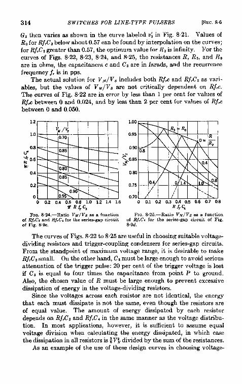
314 SWITCHES FOR LINE-TYPE PULSERS [SEC. 86
G,thenvaries as shown in thecurve labeled vj in Fig. 8.21. Values ofRO for Rf,Ca below about 0.57 can be found by interpolation on the curves;for Rf,CS greater than 0.57, the optimum value for Rs is infinity. For thecurves of Figs. 8.22, 8“23, 8.24, and 8.25, the resistances R, Rs, and RO
are in ohms, the capacitances c and Cs are in farads, and the recurrencefrequency f, is in pps.
The actual solution for V~/Vs includes both Rj# and Rf,Ca as vari-
ables, but the values of V~/ V~ are not critically dependent on Rf~.
The curves of Fig. 8.22 are in error by less than 1 per cent for values ofRj& between O and 0.024, and by less than 2 per cent for values of Rfdbetween O and 0.050.
.33$ffiHXEE&
u,, - ,
4k“ F-L 0.80
Ouii0.90
0 1.2 1.4 1.6\ I N I
O 0.2 0.4 0.6 0.8 M --TR~Ca
1.00
0.95
0.90
$.0.85
0.80
0.75
0.700 0.1 0.2 0.3 0.4 0.5 0.6 0.7 0.8
R~C4
FrQ. 8.24.—Ratio VM/ Vs as a function FIG. 8.25.—Ratio VM/VS as a funciionof RjrC8 and Rf,Ci for the serie~gap circuit of Rf,Ci for the series-gap circuit of Fig.of Fig. .%9c. S.9d.
The curves of Figs. 8“22 to 825 are useful in choosing suitable voltage-dividing resistors and trigger-coupling condensers for series-gap circuits.From the standpoint of maximum voltage range, it is desirable to makeRf,CS small. On the other hand, Ca must be large enough to avoid seriousattenuation of the trigger pulse: 20 per cent of the trigger voltage is lostif C8 is equal to four times the capacitance from point P to ground.Also, the chosen value of R must be large enough to prevent excessivedissipation of energy in the voltage-dividing resistors.
Since the voltages across each resistor are not identical, the energythat each must dissipate is not the same, even though the resistors areof equal value. The amount of energy dissipated by each resistordepends on Rf,Ca and Rf,C~ in the same manner as the voltage distribu-tion. In most applications, however, it is sufficient to assume equalvoltage division when calculating the energy dissipated, in which casethe dissipation in all resistors is %Vj divided by the sum of the resistances.
As an example of the use of these design curves in choosing voltage-

SEC. 8.6] DIVISION OF VOLTAGE ACROSS SERIES GAPS 315
dividing resistors and trigger-coupling condensers, consider the circuit(a) of Fig. 8.9, and let it be required to operate at two recurrence fre-quencies., = 1000 pps and j,, = 600 pps. Assume that the dividingresistors are equal (R1 = R2 = RS = R), which is the arrangement mostcommonly used. If CS is 90 ppf and R is 4 megohms, Rf,,C3 = 0.36and Rf,,Ct = 0.22. From Fig. 8.22 the ratio V~/Vs is 0.905 for 1000 ppsand 0.951 for 600 pps. The loss in trigger voltage across C3 is about 14per cent. For R = 4 megohms and V. = 20 kv and f, = 1000 pps, 5.7watts are dissipated in each resistor Rl and Rz and 1.9 watts in Rs, if theuneven voltage distribution due to the charging current in condenserCs is considered. If the voltage is assumed to be divided equally at alltimes, the total wattage rating of Rl, Rz and RS must equal
3 vi
~ (R, + R, + R,)’
or 4.2 watts each.It can be seen from Fig. 8.22 that, at 1000 pps, VM/Vs can be increased
from 0.905 to 0.981 by making Rs = R, instead of Ra = R. However,at 600 pps, a decrease in V~/Vs from 0.951 to about 0.835 results, whichmay or may not be serious depending on the variation of 1’s with recur-rence frequency. If this variation is assumed to be such that
0.835 (V.9)600 .- = O.981(VS)1OOOpw,
and if it is desired to have the same value for V~ at both frequencies, anover-all gain in V~/ Vs is produced by setting Rs = Ro.
The curves in Fig. 8“24 for circuit (c) of Fig. 8.9 are plotted differentlyin order to show the effects of varying both coupling capacitances, C3and Cd. The variables are R If,C4 and R~f,Cs and lines of equal ratioV~/Vs are plotted for RI = Rz = Rs.
Although these curves serve as a basis for choosing the voltage-dividing resistors and trigger-coupling condensers for any given series-gapcircuit, they cannot be used to determine which circuit to use for givengaps. Experience has shown that the choice of the optimum circuitdepends on the type of gap being used and, in some cases, on the powerlevel at which the gap is to be operated. From the standpoint of making
V~/V~ close to 1 for three-gap operation, the circuit (a) of Fig. 8.9 isthe best, @) the next best, and (c) the worst. However, experience hasshown that, although Vti is not affected by variations in the division ofvoltage across the gaps, within limits, Vti for some gaps is appreciablyaltered, depending on where the trigger is coupled. These analyses haveassumed that the dynamic-breakdown voltages of the gaps are equaland remain so throughout life. The reasons why these assumptions arenot always valid are discussed in later sections.

316 SWZTCHES FOR LINE-TYPE PULSERS [SEC. 8.7
8.7. General Considerations for Gap Design.-The three fundamentalconsiderations in the design of enclosed gaps are (1) the choice of a suit-able gas or mixture of gases, (2) the choice of suitable electrode material,and (3) the determination of a satisfactory electrode geometry. Thereare many other considerations, including structural details, that are notdiscussed here.
Chm”ce of a Suitable Gas.-Deionization characteristics and chemicalactivity are of major importance in the choice of a gas. After conductingthe required pulse, the gas must deionize at a sufficiently high rate inorder that the gap will be able to hold off the network voltage that isapplied following the pulse. In other words, the reignition voltage ofthe gap at any time after the pulse must be greater than the applied net-work or switch voltage at that time. The gas molecules should alsohave no metastable states in which electrons may be trapped during thedischarge, and from which they would subsequently be released, causinga premature breakdown of the gap. During the required life of the tube,no constituent of the gas within the gap should be absorbed by or com-bine with any elements inside the tube in quantities large enough toaffect the operating characteristics seriously.
In discussing the operation of rotary gaps in previous sections of thischapter, it is pointed out that the erosion of the electrodes is severe whenthe gaps are operated in the absence of oxygen. Because of similarexperience with enclosed gaps, a gas mixture of approximately 95 per centargon and 5 per cent oxygen was used to fill the trigatron. The oxygenmaintains an oxide coating on the electrodes in the sparking area that issufficient to limit the electrode erosion encountered during the requiredlife of the tube. However, as the oxygen is thus used up by chemicalcombination, the operating characteristics of the trigatron change. Theneed of a satisfactory switch for pulsers of higher power than those inwhich the trigatron operated satisfactorily resulted in investigational ofenclosed gaps filled with various gas mixtures. The principal character-istic sought for in these investigations was stability of switch perform-ance over an extended period of operation. This work included the studyof gas mixtures such as argon and helium, argon and oxygen, heliumand oxygen, and helium, argon, and oxygen. As a result of other work2there was evolved a hydrogen-argon gas mixture that was found tohave good deionization characteristics and to be stable ~with life. Atfirst hydrogen alone was tried, but it was found that, after a few hoursoperation at low pulse currents, the tube drop during the discharge was
I C. M. Slack and E. G. F. Arnott, “Report on Enclosed Prwsure Gaps,” NDRC14-150,WestinghouseElectric Corporation,Dec. 31, 1942.
2F. S. Goucher,J. R. Haynes,W. A. Depp, and E. J. Ryder, “Spark Gap Switchesfor Radar,” Bell System Technical Journal, October 19415.

SEC. 8.7] GENERAL CONSIDERATIONS FOR GAP DESIGN 317
abnormally high and fluctuated from pulse to pulse, causing undesirableamplitude jitter in the output pulse. It was believed that this behaviordid not exist during the first few hours of operation because of the presenceof impurities in the hydrogen that aided the transfer from a glow to alow-voltage arc discharge. When argon was added to the hydrogen, thetube drop was found to remain low and constant throughout the life ofthe tube. Therefore, mixtures of approximately 80 per cent hydrogenand 20 per cent argon are commonly used. The argon acts as a stableimpurity in that it performs the same function throughout life, as didthe impurities in the tube during the first few hours before they were“cleaned up.” The current at which this high-tube drop appeared couldbe reduced by increasing the percentage of argon, within limits. Thishigh voltage drop did not appear with tubes filled with 20 per cent argonwhen conducting l-psec 100-amp pulses, but it did appear after operatingthese tubes for 25 to 50 hr with l-psec 50-amp pulses. Apparently, theabove percentage of argon was not sufficient to effect the transfer from aglow to arc discharge at a pulse current of 50 amp without the help of theimpurities present during the first few hours. Later work showed thatno argon was needed at pulse currents of about 200 amp and above.
Chtice of Suitable Electrode Materials. —The choice of suitable elec-trode materials proved to be somewhat more difficult than the choice of agas. It was found that all the tested materials eroded rapidly in thehydrogen-argon gas mixture. The rate of erosion of the electrodes inrotary gaps and in the trigatron is kept low by the presence of atough oxide coating on the surface which is constantly replenished.Studies of the erosion of several materials and combinations of materialswhen operated in a hydrogen-argon gas mixture show that the rate oferosion of the cathode depends somewhat on its geometry. Cathodeerosion appears to be directly proportional to pulse current at a given
pulse duration, but is not directly proportional to pulse duration at agiven pulse current. For example, at a constant pulse current, theerosion at pulse durations of 2 psec and 5 ~sec is about 2.7 and 8.3 times,respectively, that obtained at 1 psec.
Since all cathode-erosion studies have not been made with electrodesof the same geometry, or at the same pulse duration, it is not possible topresent the results in concise tabular form. A few statements may bemade, however, to indicate the scope and general results of the work.An ~rly investigation conducted at the Bell Telephone Laboratoriesshowed that the erosion ratea of tungsten, molybdenum, and aluminumby weight were approximately the same, and much less than that of eithergold or carbon. These values agreed with those for sputtering in theabnormal hydrogen glow discharge. A comparison made at the Radia-tion Laboratory of the erosion rates of vacuum-cast beryllium and alu-

318 SWITCHES FOR LINE-TYPE PULSERS [SEC. 8.8
minum under the same conditions showed that of beryllium to be 0.38times that of aluminum by weight and 0.58 times that of aluminum byvolume. The use of beryllium is objectionable because the erodedmetallic vapor condenses into a fluffy material that drifts around insidethe tube and causes occasional premature breakdowns of the gap. Alu-minum was chosen as the cathode material in one major type of seriesspark gap because the material sputtered off the cathode was found tobe deposited on the anode in such a way that the gap spacing stayedapproximately constant under limited operating conditions. Experi-ments have also been made with several sintered materials containingvarious oxides that have low work functions. It was found that cathodesmade by sintering 5 per cent barium oxide, strontium carbonate, orberyllium oxide with a mixture consisting of 95 per cent tungsten and 5per cent nickel or copper for a binder had an erosion rate of about 0.025times that of tungsten or molybdenum alone.1 These materials were notused as the cathode in series gaps because of the development of thesintered iron-sponge mercury cathode, which was superior to them.
Detcrmhtat~on of a S’at~sfactory Geometry .-The wartime demand foroperable tubes made it necessary to design and manufacture them beforean adequate study of the erosion problem could be made, and before amaterial could be found that solved this problem in a hydrogen-argongas mixture. Therefore, it was necessary to determine a disposition anddesign of the electrodes such that cathode erosion would have a minimumefiect on tube characteristics. This approach ,has given rise to twobasic designs for enclosed fixed spark gaps. One design has concentriccylindrical electrodes, the outer one being an aluminum cathode. Byproviding a large cathode area, the change in the electrode spacingproduced by cathode erosion can be minimized. The other design usesa mercury cathode. In order to immobilize the mercury, it is held inthe interstices of a sintered honeycomb structure of iron powder, calledan “iron sponge.” The design is such that within the operable powerrange only mercury is eroded from this cathode.
8.8. The Cylindrical-electrode Aluminum-cathode Gap.—The ratioof the diameter of the outer electrode, or cathode, to that of the innerelectrode, or anode, is made approximately equal to e, the base of naturallogarithms. With this ratio, the highest possible breakdown voltagethat does not cause the formation of corona before breakdown for agiven outside diameter is obtained, and a minimum change occurs inthis breakdown voltage for a slight change in the size or spacing of theelectrodes.
1F. S. Goucher,J. R. Haynw, and E. J. Ryder, “High PowerSerieeGape HavingSiitered Iron Sponge Meroury Cathodes,” NDRC 14-48S,Bell Telephone Labor-tories, Oct. 1, 1945.

SEC. 8.8] ALUMINUM-CA THODE GAP 319
Cathode and Anode Erosion.—If the discharge takes place at randomover the large cathode area provided by this geometry, considerable ero-sion can be tolerated before the gap spacing is changed enough to haveany appreciable effect on the breakdown characteristics of the gap. Infact, cathode erosion is not a problem in a gap of this type, except insofaras it affects the buildup of material on the anode.
These gaps are operated in a vertical position with the cathode open-ing downward in order to allow the material eroded from the cathode thatcondenses before reaching the anode to fall to the bottom of the tube.In spite of this arrangement, it has been found that a considerable fractionof the material eroded from the cathode per pulse is transferred to anddeposited on the anode, which thus becomes coated with aluminum.For this reason the choice of anode material is not critical, and both ironand nickel have been used. The anode is not subjected to positive-ionbombardment during the main pulse; thus, anode erosion can take placeonly if there is reverse current in the circuit. In the usual designs forline-type pulsers, therefore, anode erosion does not impair the operationof a tube of this type. There are two results of the buildup of aluminumon the anode that can render the operation of the gap unsatisfactory. Ifthe amount of material deposited on the anode per pulse is great enoughto affect the voltage gradient at the anode appreciably, subsequent dis-charges take place to particular points on the anode, instead of beingdistributed over the entire surface in the sparking region. This poordistribution of the sparks causes the aluminum coating on the anode tobe rough, instead of smooth. For a gap of a given design, there is aquantity of material Ml deposited on the anode per pulse such that theanode buildup is a smooth coating for all values less than Ml. Thereis also some value Ma, greater than M 1, such that for all values greaterthan Ml such a large fraction of subsequent discharges takes place froma few points on the anode that the material is deposited in the form of“ spikes, ” rendering the gap inoperative in a short time. For values ofanode deposit between Ml and M2, predominant spikes are not formed,but the deposit of aluminum on the anode is so rough that the dynamic-breakdown voltage of the gap, and hence the operating-voltage rangeof the switch, is decreased appreciably.
Even with a smooth anode buildup the operation of these gaps maybecome unsatisfactory before the end of their required lifetime. Ifthe smooth coating is very thick, a piece may break off, particularly fromthe end of the anode, when it is subjected to shock and vibration. Thecrater thus formed on the anode causes erratic operation of the gap. Inshort, for satisfactory operation of a gap of given design, there is anupper limit to the amount of material that can be deposited on the anodeper pulse and to the total amount of material that can be deposited on
320 SWITCHES FOR LZNE-TYPEPULSERS [SEC. 8.8
the anode during the required life of the gap. Despite the fact that anodebuildup is a very serious defect in the cylindrical-electrode aluminum-cathode gap, there are many combinations of operating conditions forwhich a tube of this type is satisfactory.
Some conclusions concerning the effects on cathode erosion and anodebuildup of variations in recurrence frequency, pulse current, pulse dura-tion, gas pressure, and gap spacing are stated here. These conclusionsare based on data taken for gaps having 0.200-in. and 0.330-in. spacings,similar to the WX3226 and WX3240 gaps respectively, and filled with80 per cent hydrogen and 20 per cent argon to total pressures in the rangeof 68 to 175 cm of mercury. The ratio of the cathode radius to the anoderadius was maintained at approximately e for all gaps studied. 1
The amounts of cathode erosion and anode buildup per pulse werefound to be independent of the recurrence frequency in the range 200 to1200 pps.
For a given gap spacing, pulse duration, and gas pressure, the cathodeerosion and anode buildup per pulse were found to be directly propor-tional to pulse current in the range 100 to 400 amp.
For a given gap spacing, pulse current, and gas pressure, the cathodeerosion and anode buildup per pulse increase much more rapidly than thepulse duration in the range O.9 to 5 psec. As a result the maximumallowable pulse current for a given gap design decreases rapidly withincreasing pulse duration.
The ratio of anode buildup to cathode erosion per pulse was found toremain constant for a given gas pressure and gap spacing, even thoughthe pulse current varied from 100 to 400 amp, the pulse duration variedfrom 0.9 to 5 psec, and the recurrence frequency varied from 200 to1200 pps, corresponding to a variation from 25 X 10_’ to 560 X 10-8 mgin the mass of aluminum eroded from the cathode per pulse.
For a given gas pressure, pulse current, and pulse duration, an increasein gap spacing was found to decrease the amount of material eroded fromthe cathode per pulse, and the ratio of anode buildup to cathode erosionper pulse. A tube with large spacing may therefore be operated satis-factorily at higher values of pulse current and longer pulse durationsthan a tube with smaller spacing.
For a given gap spacing, pulse current, and pulse duration, an increasein gas pressure was found to increase the cathode erosion per pulse slightly,and to increase the ratio of anode buildup to cathode erosion per pulseappreciably. The increase in cathode erosion is perhaps due to a decreasein the size of the cathode spot with increasing gas pressure, which increasesits temperature, and thus increases the amount of material evaporatedfrom the cathode per pulse. Because the temperature along the arc
1J. R. Dillingrr, “ C.eneral Chnractrristirs of Aluminum-cathode Type SeriesSpark Gaps,” RL Report No. 682-3, Nov. 21, 1945.

L!!EC. 88] ALUMIN fJM-CA THODE GAP 321
column is high and the gas density is therefore low, and because a highergap- fillir.g pressure causes a region of higher gas density to surround thearc column, it is believed that the higher pressure aids in funnelingaluminum vapor from the cathode across to the anode. The higherpressure thus concentrates the distribution of aluminum vapor from thecathode spot in the direction of the anode.
Particular Designs jor Enclosed Fixed Spark Gaps.—The photographsof Fig. 8.26 are of five different cylindrical-electrode aluminum-cathodegaps. Photographs(a), (b), (c), (d), and(e), in Fig. 827a rex -rayprintsof the 1B29, 1B22, lB31, WX3226, and WX3240 tubes respective~y.
FXQ. 8.26,—Photographs of various aluminum-cathode gaps. (Parts (a) and @) courtesyof the Bell Telephone Laboratories. )
The 1B29, 1B22, and 1B31 were made by the Western Electric Co.whereas the WX3226 and WX3240 were made by the WestinghouseElectric Corporation.
As the required pulse current and pulse duration increased, it becamenecessary to develop gaps with larger spacings in order to limit the amountof material deposited on the anode per pulse. Since the gap dissipationincreases with spacing, it is desirable to keep this spacing to a minimum,compatible with the allowable rate of anode buildup. Therefore, it isundesirable to operate a gap at pulse currents and pulse durations thatare appreciably lower than the design figures.
After the spacing of one of these gaps has been chosen with regard toanode buildup and dissipation, the breakdown voltage can be adjusted tothe desired va!ue by changing the gas pressure. The operation of gapsfilled with 80 per cent hydrogen and 20 per cent argon has been satis-factory over a range of pressures from 50 to 250 cm of mercury. 1
‘ E. G. F. Arnott, “ Developmentof SeriesSparkGaps,” NDRC 14-327,Westing-house Electric C~cgration, Aug. 14.1944.
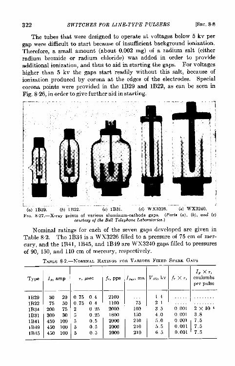
322 SWITCHES FOR LINE-TYPE PULSERS [SEC. 8.8
The tubes that were designed to operate at voltages below 5kv pergap were difficult to start because of insufficient background ionization.Therefore, a small amount (about 0.002 mg) of a radium salt (eitherradium bromide or radium chloride) was added in order to provideadditional ionization, and thus to aid in starting the gaps. For voltageshigher than 5 kv the gaps start readily without this salt, because ofionization produced by corona at the edges of the electrodes. Specialcorona points were provided in the 1B29 and lB22, as can be seen inFig. 8.26, in order to give further aid in starting.
.
L(a) 1B29. (b) 1B22. (c) 1B31. ‘“’(d) WX3226. “--(e) WX3240. -
FIG. S,27.—X-ray prints of various aluminum-cathode gaps. (Parts (a), (b), and (c)courtesv of ths Bell Telephone Laboratories. )
Nominal ratings for each of the seven gaps developed are given inTable 8.2. The lB34isa WX3226filled toa pressure of 75cmof mer-cury, and the 1B41, 1B45, and lB49 are WX3240 gaps filled to pressuresof 90, 150, and 110 cm of mercury, respectively.
TABLE82.-NOMINAL RATINGSFORVARIOUSFIXEDSPARKGAPS
Type
1B291B221B341B311B411B491B45
Iv, amp 7, psec
——
30 20 075 0475 50 0.75 0 4
200 75 2 0.25300 30 5 0 25450 100 5 0.5450 100 5 0.5450 100 5 0.5
fry PPS
2100110020001600200020002000
751601.50210210210
[’S17,kv jr XT,
-
142135 6“60140 0.00150 0 001
5.5 0.001
6.5 0 001
1, X,,
coulombspcr pulse
., ..,,..
2 x 10-43.87.57..575

SEC.8.8] ALUMINUM-CA THODE GAP 323
When more than one value is given, the second value denotes theminimum allowable value of that quantity, whereas a single value or thefirst of twovalues denotes themaximum allowable value. In twistable,1, is the pulse switch current, 7 is the pulse duration, j, is the pulse recur-rence frequency, l=,. is the average pulse switch current, and VsC is thenominal operating voltage per gap, which can be relied on during at least500 hours of operation. If two or three gaps are used in series with reso-nant charging, the nominal operating switch voltage is about 2Vsff and3VSG respectively. The usable range of operating voltage above andbelow V,. depends on the operating conditions. It is sometimes advis-able to have a nominal operating voltage above or below V~a in order tooperate more nearly in the center of the operating-voltage range.
Since lP, r, and j, are interrelated insofar as their effect on the opera-tion of these gaps is concerned, it is necessary ta state limits on the prod-ucts of these quantities taken two at a time. The product T.f, is theduty ratio, 71P is the number of coulombs per pulse. It is evident that,in order to prevent the growth of spikes on the anodes, the pulse currentmust be decreased when the pulse duration is increased. A limit on theproduct j,lp is included in the limit on I ~.., which, together with the dutyratio, limits the gap dissipation and the total amount of material depositedon the anode during life.
Change in Characteristics during Operation.—The dynamic-breakdownvoltage of each gap decreases during life because of changes in thecharacteristics of the electrode surfaces that result from the erosion of thecathode and the buildup of material on the anode. The magnitude ofthis decrease depends on the rates of cathode erosion and anode buildup,which in turn depend on tube parameters and operating conditions, asdiscussed previously. Tests show that, for a large rate of anode buildup,the value of l’~ foura set of gaps decreases during the first 100 hr of opera-tion, and then remains very nearly constant for the remainder of a 500-hrperiod or longer. For a small rate of anode buildup, V~ has beenobserved to remain constant during operating periods more than 500 hrlong. For intermediate rates of anode buildup, V.,, may decrease gradu-ally for more than 500 hr. The values of V~,, and V,ti,, are only slightlyaffected by these changes in electrode-surface conditions.
Figure 8.28 shows the variation of operating voltage range with timefor a set of three 1B41 gaps operated in series ~vith different triggercouplings as the switch in a 25-ohm line-type pulser at a pulse recurrencefrequency of 300 pps and a pulse duration of 2 psec. The operatingswitch voltage was 15.8 kv, making the pulse current approximatelyequal to 300 amp. The HK7-nulgnetron load used for the test wasreplaced by a resistance load for purposes of measuring the voltage range..k trigger voltage of 20 kv, measured on a 15 ppf load, was sufficient to

324 SWITCHES FOR LINE-TYPE PULSERS [SEC.8.8
obtain the maximum range from these gaps. It is seen from Fig. 8.28that both V~. and V,~,, are appreciably lower when the trigger is coupledto both intermediate points than when it is coupled to either the upper orlower point. This test and others show that the value of V.,, for newtubes with two-point triggering is lower than that for one-point triggering.After the electrodes become roughened, however, the difference becomesnegligible, and, because of corona bursts in the gaps after the electrodeshave become roughened, it is impossible to predict which method oftriggering will give the highest V~. The assumption that the gaps behaveas condensers, made in discussing the division of voltage across the gaps
24
20
~= 16.- — Operating vol tagew
>s~
A Triggered as in Fig, 8.9a4 —
o Triggered as in Fig. 8.9b● Triggered as in Fig. 8.9c
00 100 200 300 400 500Time in hours
1:,(;.828--- O1,miit,,)gra,,gc:,,a f{l,l{tion 0[ Ilouw of Oi,ct’;lll<,ll f,,r tllc 11141.
for each method of triggering, does not hold aftcu the electrodes Imvebecome roughened. Since 1’,,,,,,.,m(l 1’.,.,, :Ire lo\ver, :m(l over:1 long periodof time 1’3, is almut tile same \rlictll(,r the trigger is w(Iplc(l to bothpoints or to either the upper or Iotver point, it i’olloI\s tl]:it tlvo-p(]inttriggering generally gives the ]videst range of opemt ion for tIlr(>vgxpsm srrles. l
Gap Dissipation-By connecting tllc vertic:~l plates of a n]()(ii[imisynch roscope directly across the gtwun(kxl g:lp in the pIIlser s\vitcll,
the Yoltage drop across a singk g:lp (iuring the (Iisclmrgr w:w (deter-mined. The oscilloscope traws ]vere ol)scr~-e(i with s(,lf->vl)(hl)lol]olls”operation of the oscilloscope, that is, the sigm~l Yolt:qq :Ll)~)li((i to thr

$hc. S.8] ALUMINUM-CA THODE GAP 325
vertical plates was also used to start the sweep. Because there is aslight time lag between the application of the voltage starting the sweepand the appearance of the trace on the oscilloscope screen, the initialportion of the voltage pulse cannot be observed. The curves in Figs.8.29 and 8.30 were drawn from these traces, and show the voltage drop
m
240 \
mSpecing
$160 \
\ /375 roils
.E 120 > \ ,
F200 roils
=s0$1=40
o 1
+)~O 02 0.4 0.6 0.S 1.0 1.2
Time in A sec
280
240
1
200
160 1g$.E 120m
; 808s
40 Y \
o \
-40 A
Current pulse <
-80 1
0123456Time in A sec
Fx~.8.29.—Voltage drop acroee three FIG. S.30.—Voltage drop across threefixed spark gaps having different electrode fixed spark gaps having different electrodespacings for a pulse duration of 0.9 ~sec. spacings for a pulse duration of 4.5 psec.
across each of three gaps having different electrode spacings for nominalpulse durations of 0.9 and 4.5 ysec, respectively. The gaps with spacingsof 150, 200, and 375 roils were, respectively, the 1B22, WX3226, and a gapsimilar to the WX3240, but with a slightly greater spacing. The cor-responding current pulse is also shown; the rounding of the leading edgeof the current pulse is a result of the high tube drop during the first part,of the pulse.
The tube drop was found to be independent of the gas mixture, thegas pressure, the pulse current, and the recurrence frequency within thelimits of error of these measurements, and within the range over whichthese quantities were varied. The gas mixture was varied from ] 00 percent hydrogen to 100 per cent argon, the pressure from 68 to 150 cm ofmercury, the pulse current from 80 to 240 amp, and the recurrence fre-quency from 200 to 2000 pps. The tube drop is primarily dependent onthe electrode spacing and pulse duration.
The voltage across a gap during the first part of the discharge has

326 SWITCHES FOR LI,VE-TYPE PULSERS [SEC.8%
been studied with the use of a capacitance voltage divider. By multiply-
ing the values of tube drop and pulse current for each increment of timeduring the pulse, a curve can be obtained showing the rate at ~vhichenergy
75,
n
60
~ 45 \c.-=$30 1
15 \
~
00 0.2 0.4 0.6 0.8 1.0Time in ,u sec
FIG. S.31 .—Power dissipated in oneWX3226 gap as a function of time fora single pulse.
is dissipated in a single gap during thepulse. Figure 8.31 shows such a curvefor a WX3226 gap operated in serieswith two other gaps at a pulse dura-tion of 0.9 psec and pulse current of 80amp. Integrating this curve, a valueof 15.4 X 10⁻³ joules is obtained asthe energy dissipated per pulse in oneof these gaps. A measurement of theaverage dissipation by means of a cal-orimeter gave a value of 15.5 X 10⁻³joules per pulse. A comparison ofother values obtained by integratingpower-versus-time curves with thoseobtained calorimetrically also showsgood agreement.
The dissipation per pulse has beenfound to be directly proportional to
pulse current and ta gap spacing. By arbitrarily assuming that anequation for dissipation per pulse involves terms including 7 and +,the follo\ving empirical relation has been developed:
D = (0.703 X 10⁻⁶ + 0.420, – 0.0233 X 10’,’)SIP,
where D is the dissipation per gap in joules per pulse, 7 is the pulse dura-tion in seconds, S is the gap spacing in roils, and 1= is the pulse current inamperes. This equation agrees reasonably well with experimental dataover the range of 0.9- to 5.O-~sec pulse duration, 0.200 to 0.440-in. spac-ing, and 80- to 500-amp pulse current. 1
Time Jitte~.—Attempts to make the cylindrical-electrode aluminum-cathode gap operate synchronously have not been successful. In usingthese gaps 1 to 3 psec of over-all time jitter must be tolerated, dependingon operating conditions and particularly on the value of the operatingvoltage relative to V~ and V~im. About 95 per cent of the pulses show atime jitter that is considerably less than 1 psec, but an appreciable num-ber of random pulses account for the over-all jitter of 1 to 3 psec.
The two gaps in a set of three that are broken down by the trigger
1R. G. Fluharty and J. R. Dillinger, “Dissipation in Series Spark Gaps andVoltage-currentRelationshipsDuringthe Discharge,” RL Report N’o.682-1, June26,1945.

SEC. 8.9] THE IRON-SPONGE MERCURY-CATHODE GAP 327
pulse can be made to fire accurately to within 0.1 psec. The primarysource of jitter in a switch of this type isin the firing of the third tube,which cannot be overvolted by the trigger. After the two triggered tubesare broken down, the full switch voltage is applied to the third tube;thus, the greater the switch voltage, the greater the overvolting of thethird tube. The jitter in this switch, therefore, decreases with increas-ing switch voltage. At a given switch voltage the jitter also variesduring the life of the tube because of changes in electrode-surfaceconditions. 1
8.9. The Iron-sponge Mercury-cathode Gap.—A gap of this type2is an improvement over the cylindrical-electrode aluminum-cathode gapin at least three respects:
1. The range remains constant during life. o2. The time jitter can be maintained at a value of the order of mag-
nitude of one per cent of the pulse duration.3. As wide an operating range can be obtained with two of these gaps
as with three of the cylindrical-electrode aluminum-cathode gaps.
For satisfactory operation, however, the reverse current must be keptvery low.
The anode of this gap is a molybdenum rod with a diameter of approxi-mate y 0.060 in. The cathode is mercury that is immobilized by an ironsponge. This iron sponge contains about 60 per cent void space and ismade by compressing iron powder into a kovar cup and sintering underappropriate conditions. After subsequent heat treatment in a hydrogenatmosphere the sponge of a typical gap holds about 9 cm3 of mercurywhen fully saturated. The mercury that is evaporated from the surfaceof the cathode during operation condenses and runs down the walls backinto the sponge. Because of the surface tension of the mercury, a film ofmercury is maintained over the surface of the iron sponge which preventsthe erosion of the iron. In order to minimize the time jitter, the gaps areusually filled with 100 per cent hydrogen. Radium salts are generallyomitted in order to increase the operating range and to further minimizejitter.
1H. L. Glick, “Triggering of High Power Spark Caps,” WestinghouseResearchReport SR-307, Oct. 18, 1945.
t F. S. Goucher,J. R. Haynes,and E. J. Ryder, “ High PowerSeriesGaps HavingSintered Iron Sponge Mercury Cathodes,” NDRC 14-488, Bell Telephone Labora-tories, Oct. 1, 1945; J. R. Dillinger, “Operation of SinteredIron Sponge-MercuryCathodeType SeriesGapsat 5 MicrosecondCondltioas,” RL Report N-o.682-5, Nov.28, 1945; and J. R. Dillinger,“Line-Type Modulatorand HP] OV MagnetronOperrt-tion at 6 Megawatts,” RL Report No. 682-6, Nov. 30, 1945.

1328 SWITCHES FOR LINE-TYPE PULSERS [SEC. 89
Particular Gap Designs. —Figure 832 shows the two tubes of this typedeveloped to date. The cooling fins, which are in thermal contact withthe cathodes of the tubes, can be seen. The 1B42 is shown in Fig. (8.32a and the Fe-I is shown in Fig. 8.32b. The large opaque spot just
I
L
.- .- -. ------.——.
(
(a)
II
!
(b)FIG. 8.32.—Photographsand X-ray prints of iron-spongemercury-cathodegaps.
(a) The 1B42, (b) the Fe-I. (The photograph for prt (a) courtesy of the Bell TelephoneLaboruforiea.)

SEC. 8.9] THE IRON-SPONGE MERCURY-CATHODE GAP 329
above the kovar cup in the x-ray of the Fe-I tube is due to a globule offree mercury that collected there when the tube was placed in a horizontalposition to take the x-ray. The small spots on the walls of the kovar cupwere caused by drops of mercury adhering to the kovar. The upperportion of the anode is surrounded by grass shields in order to preventmercury from dripping down close enough to the sparking region to affectthe operation of the gap. The 1B42 is mounted by means of a boltextending down from the cathode, and the cooling fin is an integral partof the tube. As shown in the sketch in Fig. 8.32b, the cooling fin of theFe-I tube is not an integral part of the tube, but serves instead as amounting socket. The operation of the Fe-I tube with various electrodespacings and gas pressures has been satisfactory for a variety of condi-tions, the reliable life of the tube being greater than 500 hr.
Some specifications for these tubes are given in Table 8.3. Eachquantity has the same significance as in Table 8“2. In columns contain-ing more than one figure, the first represents the maximum and the secondthe minimum rating. The value of Vsa, the nominal operating voltageper gap, has been obtained from data for the operation of two gaps inseries.
TABLE8.3.—RATINGSI-ORTwo IRON-SPONGEMERCURY-CATHODEGAPS
VSG,TIP, f,IP,
No. I,, amp 7, psec f,, pps 19.., ma ~v Tf, coulombs amp Xper pulse see-l
1B42 3*8O 6.1-0.25 2000 0.250 5.0 0.0012 1,28 X 10-s 40 x 104Fe-I 750-100 5.54.5 1000 0.45Q 7.5 0.0011 1.5 x 10-~ 25 X 104
Operating Characteristics. —T~Vo of these gaps are used in series asthe switch in a line-type pulser because it was found that two gaps give anoperating range greater than *33 per cent, which is ample for mostapplications. In general, one would expect Vti~ to be equal to the break-down voltage of one gap and VS to be twice this value when using twogaps in series, making the range +33 per cent. However, the applica-tion of the charging-voltage wave to these gaps causes a corona sheathto be formed about the anode, which changes the breakdown characteris-tics. The magnitude of this change increases with the amplitude of thecharging-voltage wave. At voltages near Vti~, the corona- sheath has asmall effect, and the breakdown voltage of the gap is approximatelycharacteristic of a point-t~plane discharge, as seen from the x-rays ofFig. 8.32. N’ear Vs, however, the corona sheath is large and shapedlike a distorted sphere about the end of the anode, making the breakdownvoltage per gap more nearly characteristic of that of a sphere-to-planedischarge. Thus, the dynamic-breakdown voltage per gap at voltages

330 SWITCHES FOR LINE-TYPE PULSERS [SEC. 8.9
in the region of Vs k greater than in the region of voltages near Vrnim.
Therefore, the ratio of Vsto Vti~isgreater than2to lfor the operationof two gaps in series. If a small amount of radium salt is inserted inthese gaps, the beneficial effects of this corona sheath are destroyed, andthe ratio of maximum to minimum operating voltage obtained with twogaps becomes less than 2.
For two Fe-I gaps operated at 15.5 kv, 290 amp, 300 PPS, and 2 psec,the voltage range of 10.5 to 22.5 kv is constant for more than 500 hr ofoperation, with V,~,t equal to 5.5 kv. The required trigger voltage is20 kv, and the time jitter is less than 0.02 Psec at voltages above 14 kv,provided that the rate of rise of trigger voltage is 55 kv/ysec or greater.For gaps filled to higher gas pressures, ranges of 13 to 29 kv for two gapshave been maintained during more than 500 hr of operation at 24.5 kv,925 amp, 250 pps, and 2 psec.
Time Jitter.—In operating two gaps in circuit (d) of Fig. S.9, gap Gz isbroken down by the trigger pulse, applying the full switch voltage toGl, which is then broken down. If the delay in firing G, is appreciable,Gz can partially recover and must be reignited after G* breaks down.As a result, there are at least three sources of uncertainty-in the initiationof the discharge, which combine to produce the observed time jitter inthe output pulse.
The uncertainty in the firing of G2 by the trigger pulse can be madesmall compared with 0.02 psec by making the rate of rise of the triggervoltage pulse equal to or greater than 55 kv/psec.
The uncertainty in the firing of G, can be reduced by increasing theswitch voltage, all of which appears across GI after Gz breaks down.The time jitter introduced in reigniting Gz has been detected, but it isnegligibly small.
All three sources of time jitter, but particularly that introduced inthe firing of Gl, can be reduced by improvements in the tube design.The elimination of argon from the gas filling, a reduction in the diameterof the anode, and a decrease in the gap spacing have all been found effec-tive in reducing time jitter. It is possible to eliminate argon from thesetubes because they are intended for operation at pulse currents of 100amp and higher. A reduction in the anode diameter decreases the jitter,but increases the detrimental effects of reverse current in the tubes. Themost effective way of reducing time jitter is to decrease the spacing, andto increase the gas pressure accordingly in order to obtain the desired gapbreakdown voltage. However, the maximum gain that can be obtainedby this method is limited because, for a gap with small spacing, the break-down voltage increases linearly with gas pressure in the region of lowvalues, but for high gas pressures, this voltage is not affected appreciablyby a change in pressure.

SEC. 8.9] THE IRON-SPONQE MERCUlt Y-CATHODE QAP 331
Effects of Rever8e Current.-Reverse current damages iron-spongemercury-cathode tubes by erodhg the electrode that is the anode forthe forward pulse and the cathode for the reverse current pulse. Theresulting increase inspacing during operation causes Vtito increase andVs either toincrease or to decrease. If considerable materialism erodedfrom the anode and deposited on the tube walls, mercury condenses on itand partially covers the walls. This mercury may give rise to disturb-ances along the walls, which can lower 1’s despite the increase in spacing.The increase in spacing also causes the time jitter to increase. Testshave shown that a given value of reverse current has a more detrimentaleffect on gap operation from the point of view of time jitter than fromthat of operating range. In order to specify the reverse current that canbe tolerated in these tubes, limits are imposed on the maximum value oferosion per pulse and on the total erosion permissible for a life of 500 hr.The film of mercury that coats the end of the anode during operation hasbeen found ta limit the erosion rate of the anode to a value much smallerthan would be obtained without this film. It is therefore necessary tolimit the amount of erosion per pulse of reverse current, otherwise themercury film could be broken through during a single pulse of reversecurrent, thereby exposing the molybdenum of the anode and greatlyincreasing the erosion rate. By placing limits on the pulse current andthe pulse duration the erosion per pulse can be limited, If the totalerosion during a period of 500 hr were directly proportional to the num-ber of coulombs per pulse, it could be limited by a specification of themaximum allowable value of the average current. Although this linearrelation does not hold over a wide range of pulse duration, the linearity issufficient for general specifications. The limiting value of the averagereverse current that does not affect time jitters appears to lie between1 and 2 ma.
In addition to the need for limiting the reverse current in these tubesto a very low value because of its effect on range and time jitter, it isnecessary to limit it in the tubes filled with 100 per cent hydrogen inorder to eliminate amplitude jitter. In tubes containing 100 per centhydrogen, the tube drop during the conduction of reverse currents of lowpeak value can be high and can fluctuate from pulse to pulse. A volt-age that is sufficient to affect the next charging voltage can therefore beleft on the network after the pulse. Since the amount of voltage lefton the network fluctuates from pulse to pulse, amplitude jitter can resultin the output pulse.
Dissipation.-As a result of calorimetric measurements made at theBell Telephone Laboratories’ on iron-sponge mercury-cathode gaps
1F. S. Goucher,J. R. Haynes,W. A. Depp, and E. J. Ryder, “Spark Gap Switchesfor Radar,” Bell S@em Technical Jourrud, Oct. 1946.

332 S WITCHES FOR LINE-TYPE PULSER,~ [Sm 8.10
operated over a wide range of pulsing conditions, the following empiricalformula has been established expressing the dissipation D in j(JUICS perpulse per gap in terms of the gap parameters and the pulsing conditions:
D = 5.7 X 10-71=S + (40 + 3.9 X 10⁻²p04S)1,,,,
where 1= is the pulse current in amperes, S is the gap spacing in roils, p
is the gas pressure in inches of mercury, and r is the pulse duration inseconds. This equation has been established from data covering thefollowing ranges of parameters: spacing, 40 to 350 roils; gas pressure, 28 to50 in. of mercury; pulse duration, 1 to 6 psec; pulse current, 45 to 1070amp. The dissipation in watts per gap for any application may beobtained by multiplying the value of D by the recurrence frequency.This equation does not include the energy contributed by the trigger,which can usually be neglected, but which can be measured independentlyand added if necessary.
Dissipation is an important consideration not only from the stand-point of circuit efficiency, but also in determining whether or not forcedcooling is necessary when operating mercury-cathode gaps. Sincemercury vapor has poor deionization characteristics, there is some upperlimit to the partial pressure of mercury, and thus to the operating tem-perature of the gap, above which the poor deionization characteristicsof the mercury override the good characteristics of the hydrogen.
8.10. The Three-electrode Fixed Spark Gap.—In order to build asatisfactory three-electrode gap, it is necessary to have an electrodematerial such that its erosion rate at the desired operating conditions isnegligibly small in the gas to be used. Since a gap of this type has asomewhat more complex electrode configuration than does a two-elec-trode gap, much less electrode erosion can be tolerated.
The Trigatron.-The trigatron’ is a three-electrode tube filled withapproximately 95 per cent argon and 5 per cent oxygen to pressures ofabout 1 to 6 atmospheres, depending on the desired operating voltageand on particular tube design. The British CV85 and the CV 125 werethe two most widely used designs. Typical operating conditions for theCV85 are 8 kv, 1200 pps, and 1 psec in a 70-ohm line-type pulser.Photograph (a) of Fig. 8.33 shows a CV125 and (b) is a print of anx-ray of this tube. The anode and cathode are of molybdenum and thetrigger pin is tungsten. The anode sleeve was found effective in makingthe time jitter less than 0.1 ~sec.
Oxygen is used in a trigatron principally to maintain an oxide coating
1J. D. Craggs, M. E. Haine, and J. M. Meek, “The Developmentof TriggeredSparkGapswith ParticularReferenceto SealedGaps,” Metropolitan-VickersElectricCo., Ltd., Report No. C-331, September1942.

SEC. 810] THE THREE-ELECTRODE FIXED SPARK GAP 333
on the surfaces of the electrodes and thereby to limit the rate of electrodeerosion, since there are effectively two cathodes in the tube when it isoperating. In this tube, the principal discharge does not start betweenthe anode and cathode after the tube is triggered, but takes place fromthe cathode to the trigger pin to the anode. Thus, the trigger pin mustserve as both an anode and cathode, and is therefore doubly subject toerosion. Because of the small size of the trigger pin and the other elec-trodes, this erosion must be minimized. The oxygen is also needed inthese gaps to quench metastable atoms of argon after the discharge.
.-!
I
..—.-.(a) (b)
F]o. S.33.—(a) A photograph and (b) an x-ray print of the CV 125 three-electrode gap.
At a recurrence frequency of 800 pps and a pulse duration of 0.9 psec,and in a line-type pulser with a 50–ohm network and 50–ohm load, anew CV85 trigatron has a range of about 3.5 to 11 kv with a startingvoltage of 1.5 kv. A trigger voltage of 6.5 kv is sufficient. The curvesof Fig. 8,34a show the variation in range with trigger voltage for a newCV 125 operated in this circuit. A comparison of these curves withthose of Fig. 8.11 for three WX3226 gaps filled to a pressure of 110 cm ofmercury and operated under the same conditions shows that the range ofa new CV 125 is equivalent to that of three of these gaps in series.
Figure 8.34b shows variations in range with life for a Cl’ 125 operatedat 12 kv, 800 pps, and 0.9 Psec in a 50-ohm circuit. After 375 hr of

334 SWITCHES FOR LINE-TYPE P ULSERS [SEC. 8.10
operation, this tube was found to fail to deionize at frequent intervals,agreeing with British experience. Failure of this tube is not due toelectrode erosion, for it operates satisfactorily after being pumped andrefilled. The failure may be due to the formation of nitrogen peroxide,which is known from experience with rotary gaps to have poor deioniza-tion characteristics, or it may be due to a reduction in the amount ofoxygen to a value that is insufficient to quench metastable atoms of argonafter the discharge. This reduction is caused bv the combination ofoxygen with the molybdenum and tungsten electrodes during operation. 1
20rTPrF7
I I I I‘5tart
I%11
10 12
20
vma.
~ 15 \ —c
Operating&Z voltage
~ 10
c:
~ v
5 -- fmn
&
vstari
04 100 200 300 4.-Trigger vr-ltageIn k;-
(a)FIG. S34.-Variation in voltage range of a CV125 three-electrode
voltage (new tube), (b) with time.gap (a)
Timemhours(b)
with
)0
trigKer
Further comparison of the CV125 with a set of three WX3226 gapsopcrat ed under the same conditions at a pressure of 110 cm of mercuryS11OJVSthat a 13-kv trigger voltage is required to obtain the lolvest valuesof 1‘,,,,” and J’,,.., for the series gaps, ~vhcreas 8 kv is sufficient for thethree-clcctrodc gap. It is also to be noted that the CY125 requires ahigh trigger voltage primarily for good starting, ~vhereas series gapsre(luirc a high trigger voltage to give a satisfactory operating range as\\-rIl. The time jittm in the CV125 at 12 kv, 800 pps, and 0.9 pscc in a50-ohm circuit remains less than 0.09 psec throughout life, a value thatis much less than that for cylindrical-electrode aluminum-cathode gaps.The Iifc of series gaps under the abo~-e conditions is considera})ly longerthan that of the C}”125, and can exceed 1500”hr. .41s0, the deionizationcharacteristics of the series gaps arc better than those of the trigatrons,
I These ohscrv ations are in accord with reports of work done by thr llrltish atBirmingham ~niversity, See D. T. Itobcrts, “ Dctcrrnination of Oxygen and Xitro-gell Pcroxldc in Samplesof Gas from Trigatrons Taken at Various Stages of Iife,”Birn,inghamUniversity,C. V. D. Report BS/19, 1943.

SEC.8.10] THE THREE-ELECTRODE FIXED SPARK GAP 335
as is evidenced by the greater decrease in V~ with increasing recurrencefrequency for the trigatron than for the series gaps.’
Hydrogen-$lled Three-electrode Gap.—It would be desirable to combinethe advantages of the hydrogen or hydrogen-argon gas filling, which mstable with life, with those of a three-electrode geometry of thetrigatrontype. Unfortunately, the erosion rate of possible electrode materialsin the absence of an oxide coating on the surface is usually high.
An attempt has been made to overcome this difficulty by usingelectrodes made by sintering tungsten and barium oxide together,withnickel as a binder. Statements concerning the erosion rate of thesesintered mixtures have been given in Sec. 8“7. Some three-electrodetubes have been constructed with these materials, but sufficient testshave not yet been made to indicate the stability of their characteristicsduring life.z
THE HYDROGEN THYRATRON
BY K. J. GERMESHAUSEN
As explained in the introductory paragraph of this chapter, work wasstarted early in the history of the development of pulse generators inorder to obtain a satisfactory switch of the thyratron type. The advan-tages of the thyratron are many: the switch is small and light, it can betriggered accurately by applying low-voltage pulses to the grid, it has ahigh efficiency, and it can operate over a wide range of plate voltages.
Experimental work was started simultaneously to improve existingmercury thyratrons and to develop tubes of new types. One disadvan-tage of mercury is its temperature sensitivity; this, however, can beremedied by thermostatic control of the enclosures. There are otherdifficulties specifically related to pulser operation, such as the long deion-izing time and the low voltage drop at which ion velocities destroy theoxide cathode. To eliminate these defects, developmental work wasstarted on a thyratron that would be particularly well suited to pulseroperation. Hydrogen was chosen for the filling because it enables highpulse currents to pass through the tube without causing voltage dropsgreat enough to destroy the cathode. Also, the structure of the tubeswas designed specifically to withstand high voltages. The develop-mental work has been successful in creating and putting into productionthree tubes that provide for a continuous range of pulse power from about10 to 2500 kw; work has also been started on a tube capable of switching
1J. R. Dillinger, “General Characteristicsof Aluminum Cathode Type SsriezGaps,” RL Report No. 682-3, Nov. 21, 1945.
~K. J. Germezhmmenand H. R. Zeller, “Three Electrode Triggered Gap,” RLReport No. S80, Oct. 11, 1945.

336 SWITCHES FOR LINE-TYPE PULSERS [SEC. 8.11
pulse powers ranging from about 5 to 8 Mw, but has not been completedat the time of this writing.
8.11. General Operating Characteristics of the Hydrogen Thyratron.The use of hydrogen in place of mercury vapor or a rare gas as the fillingfor thyratrons, 1 appeared to have some real advantage if an adequatelife could be obtained. Drewell succeeded in making hydrogen tubesfor sweep circuits, but their operating voltage and life were inadequatefor pulser applications. His results, however, were considered encourag-ing enough to warrant further development, and consequently work wasstarted in 1941.
The primary advantage of hydrogen, when used in a thyratron, isthe high fall of cathode potential that can occur without injury to theoxide cathode. The destruction voltage, or voltage corresponding tothe ion velocity at which destruction of an oxide cathode sets in, is about30 volts for mercury ions and has about the same order of magnitude forthe rare gases, including helium. For hydrogen the destruction voltageis about 600 volts, or 20 times as great. This fact is of considerableimportance in the design of a thyratron for operation at high voltagesand high pulse currents.
A second advantage of hydrogen-filled tube is the short deionizationtime that is obtained. In any given circuit this deionization time isabout one tenth that of mercury-, argon-, or zenon-filled thyratrons.The only other gas that provides such a short deionization time is helium,which cannot be used because of the cathode destruction previouslymentioned.
A serious problem connected with the use of hydrogen in thyratrons isgas cleanup, or the disappearance of the gas during operation. Gascleanup is caused mainly by the great chemical activity of hydrogen,which combines readily with many substances including, under certainconditions, the oxide cathode. The grade A nickel usually employed invacuum-tube construction contains reducing agents, such as carbon andsilicon, that combine with the hydrogen and promote cleanup. Inaddition, these nickels may contain other reducing agents, suchas magnesium, which do not combine directly with hydrogen, butwhich can reduce the oxide cathode, releasing free barium. The freebarium thus produced combines very readily with hydrogen andcan cause a rapid disappearance of the gas in the tube. In order toobtain nickel free from these reducing agents, or other harmfulimpurities, it was necessary to develop a very pure grade of electrolyticnickel.
In addition to the use of materials of carefully controlled purity, it isimportant to prevent contamination resulting from improper cleaning or
1P. Drewell,ZeAs.f. Techn. Phy.s., 16, 614, (1936).

SEC. 8.11] OPERATION OF HYDROGEN THYRATRONS 337
handling of the parts. The successful manufacture of hydrogen thyra-trons requires a much more rigid control of the various manufacturingprocesses than is usual in the manufacture of radio tubes. Great caremust be taken to prevent the inclusion of any substance that can reactchemically with the hydrogen. By proper design and processing, andby the use of selected materials, pressure cleanup has largely been elimin-ated and is no longer a serious limitation on tube life.
Since the reducing action of hydrogen on the oxide cathode becomesserious at temperatures of about 900”C, it is necessary to maintain thecathode temperature well below this value. A maximum temperatureof 850°C is permissible, but a somewhat lower value is preferable. Onthe other hand, cathode emission decreases rapidly at temperaturesbelow about 800”C; hence, the operating range of cathode temperatureis narrow. The filament voltage must therefore be kept within closelimits, and variations in cathode tem~erature from tube to tube minim-ized. ‘ Variations in temperatureover the surface of the cathode canbe made much smaller for indi-rectly heated cathodes than forfilament cathodes; hence, it is de-sirable that hydrogen tubes haveindirectly heated cathodes.
Because of gas cleanup, the gaspressure is raised as high as possibleby making the spacing between theanode and grid much smaller thanin the more conventional thyratrondesigns. The purpose of the smallspacing can best be explained byreferring to Fig. 8.35, which is a
Product of pressure in mmand spacing in mm
FIG. 8.35.—Plot of breakdownvoltagein hydrogenFMa functionof the productofspacingandpreesure.
plot of the breakdown voltage in hydrogen versus the product of spacing andpressure, the familiar Paschen curve of breakdown in gases. In thyra-trons the grid-to-anode spacing is such that the operating point is on theleft-hand portion, of the curve, where the breakdown voltage is risingrapidly as the product of spacing and pressure is reduced. Since theproduct of spacing and pressure must be maintained at a value less thanthat corresponding to the desired breakdown voltage, high gas pressurescan be obtained only by reducing the spacing. In typical hydrogenthyratrons, the gas pressure is about 500 microns and the grid-anodespacing is about 0.0625 to 0.090 in. Smaller spacings make the mechani-cal assembly difficult, and may result in field emission from the grid.The perpendicular distance from grid to anode must not exceed thedesired spacing at any point; the grid structure is therefore placed so

338 SWITCHES FOR LINE-TYPE PULSERS [SEC. 8.11
that it completely surround the anode, as shown in Figs. 8.36, 8.37, and8.38. Long-path discharges between the anode-lead wire and the out-side of the grid stmcture are prevented by surrounding the lead by a glasssleeve that fits tightly into a collar attached to the grid structure. FromFig. 8“36 it is apparent that the distance betweenthe upper part of the anode lead inside the glasssleeve and the grid stmcture is considerably greaterthan the shortest spacing from grid to anode.
F
1-::7
Breakdown over this relatively long path is pre-.,.
vented partly by the small spacing between the \ ‘1 !IL<,,I/~&glass sleeve and the anode lead, and partly by the j -J1
fact that the field between the anode lead and
r Anodelead
flhbama
M
0000
caam#a
JWd,r.
} cathode
-“ ------
1“11”1’II
Cathodeshielding
1111IllIIIII1111II,,,
FIG..S.37.—Cu&away
“.~”perspective view of the5C22 hydr~=.u .-=...
l?m. 8.36.—Structure of a hydrogen thyratron. tron.
the grid structure in this region is in such a direction that the accelera-tion of ions or electrons over the long path is prevented.
Hydrogen thyratrons differ from the more common thyratron typesin that they are designed with a positive control-grid characteristic.In order to trigger the tube it is necessary to drive the grid to a positivevoltage sufficient to draw grid current between the grid and the cathode.Two considerations dictated the positive control characteristic. First,

SEC. 8.11] OPERA TION OF HYDROGEN THYRA TRONS’ 339
positive control simplifies the trigger circuit, since, for most applications,no negative bias supply is required. Second, the extensive bafflingbetween the anode and cathode that is associated with positive controlminimizes grid-emission difficulties.
In order to obtain a positive control characteristic, the cathode iscompletely shielded from the anode field in the manner shown in Fig.8.36: The grid itself is a perforated,or mesh, section situated just belowthe anode, and beneath it is a gridbaffle, which is attached to the grid.In such a structure the anode fielddoes not extend beyond the pointmarked A, and there is no opportu-nity for the anode field to act uponelectrons emitted from the cathode,most of which are confined to theregion inside the cathode shield andbaffle structure. In order to triggerthe tube, or to start conduction, it isnecessary to draw current between thegrid and the cathode. This currentproduces electrons and ions in theregion outs id e the cathode-shieldstructure, some of which reach thepoint A. As soon as the electron den-sity at A is high enough, the anodefield is able to produce ionizationin the region above the grid baffles,and breakdown takes place. Duringthe initial stages of the breakdown,the anode current is drawn from thegrid as a glow discharge because theanode field is unable to penetrateinto the grid-cathode space. Thisglow discharge raises the grid to ahigh positive potential, which quicklyionizes the grid-cathode region to anextent sufficient to bring the grid back
FIG. S.3S.—X-ray photograph of ahydrogen thyratron.
almost to the cathode potential.The entire breakdown process described above occurs in 0.02 to 0.07psec, which is thus the ionization time.
Tube Characteristics and Operation.-Photographs of the three hydro-gen thyratrons that have been developed are shown in Fig. 8.39, andtheir basic operating characteristics may be found in Table 8.4.

340SW
ITC
HE
SF
OR
LIN
E-T
YP
EP
UL
SER
S[S
EC
.8.11

SEC.8.11] OPERA TION OF HYDROGEN THYRA TRONS 341
TABLE 8.4. —OPEEATINO CEAEACTERISTICS OF THE 3C45, 4C35, AND 5C22 HYDROGENTHYRATItONS
3C45 4C35 5C22
Maximumforwardanode voltage in kv. . . . . . . . . . . . . . . . . . 3Maximuminverseanode voltage in kv. . . . . . . . . . . . . . . . . . . 3.0hfaximumvalue of inverseanode voltage in kv for 25 ~ec
after pulse. . . . . . . . . . . . . . . . . . . . . . 1.5hlaximumanode pulse currentin amp. . . . . . . . . . . . . . . . . . 35Pulsepower into resistanceloadin kw. . . . . . . . . . . . . . . . . . . 50illaximumaverageanode currentin ma. . . . . . . . . . . . . . . . . . 45Cathode: indirectlyheated, unipotential.. . . . . . . . . . . . . . . .Heaterpower in watts. . . . . . . . . . . . . . . . . . . . . . . . . . . . . . . . . 15Heatervoltage involts (+7.5 %).... . . . . . . . . . . . . . . . . . . . 6.3hfaximumpulse durationinxec. . . . . . . . . . . . . . . . . . . . . . . . 6Grid bias in volts . . . . . . . . . . . . . . . . . . . . . . . . . . . . . . . . . . . . . ohfinimumtriggervoltage in volts.. . . . . . . . . . . . . . . . . . . . . . 150Tube weight in grain s. . . . . . . . . . . . . . . . . . . . . . . . . . . . . . . . 64Tube life atmaximum ratingsin hours. . . . . . . . . . . . . . . . . . 500
88.0
2.590
350100
406.360
150194500
1616,0
5.0325
2500200
656.360
150273500
A simplified diagram of a thyratron pulser is given in Fig. 8“40.Hydrogen thyratrons are designed to work primarily into a load
impedance of 50 ohms and, in the case of the 3C45 and 4C35, maximumpulse power is obtained at this level. The 5C22 supplies its maximumpulse power at 25 ohms; however, the average power is the same as at
Cr:ahwg;g
PUI*
c~r#! network
Trigger
D-cpower
0- —supply
FIIJ. 8.40.—A typical hydrogen-thyratron pulser circuit.
50 ohms. Any desired load impedance maybe used, provided that noneof the maximum tube ratings are exceeded. In general, both pulse andaverage power are less if a load impedance of other than the optimumvalue is used.
The life of the thyratron depends greatly on the operating voltage,current, and recurrence frequency. A typical life of about 500 hr canbe obtained at the maximum voltage and current ratings, with recurrence

342 SWITCHES FOR LINE-TYPE PULSERS [SEC. 8.11
frequencies of 2000 pps for the 3C45 and 4C35 and 1000 pps for the 5C22.The length of life is considerably increased by reducing any of theseparameters, and, in general, the operating level of thyratron pulsersshould be kept somewhat below the maximum tube ratings. A muchlonger tube life can be obtained by operating the tubes well below theseratings; for instance, 4C35’S operated at 4 kv and 45- to 50-amp pulsecurrent usually give 2500 to 3000 hours of satisfactory service. Improve-ments in manufacturing methods are constantly increasing the lifeexpectancy, which may soon beat least 1000 hr at full rating.
Since the thyratron is a unidirectional switch, negative charges areleft on the network if the load impedance is too low. When the loadimpedance varies erratically, as in the case of a sparking-magnetronload, variable negative charges may be left, which seriously affect theforward voltage of the succeeding pulse. In order to remove thesenegative charges and to minimize or prevent their effect on forwardvoltage, it is usually desirable to connect a shunt diode across the thyra-tion. The problem of unidirectional-switch operation is discussed indetail in Chap. 10.
The tube heating time may be reduced by overvolting the heater byas much as 20 per cent, in which case the preheating time for the 5C22is reduced from five to two minutes. It may also be possible to applythe anode voltage and heater power simultaneous y; however, adequatetests and recommendations from the manufacturer are necessary if thepresent ratings and specifications are not followed exactly.
Hydrogen thyratrons may be mounted and operated in any position,but care must be taken lest the life be reduced by gas cleanup or punctureof the bulb. Gas cleanup is accelerated if the bulb temperature islowered by subjecting the tube to forced cooling, or if intense r-f fieldsare present to cause the ionization of the gas. Corona extending to theglass surface causes erratic operation and, eventually, puncture of thebulb.
Series and Parallel Operation of Hydrogen Thyratrons.—It is oftenpossible to satisfy switch requirements for which no single thyratron issuited by the operation of two tubes in series or in parallel. 1 Paralleloperation provides twice the load current, while series operation providestwice the load voltage. There are a number of possible circuits, two ofwhich are shown in Figs. 8.41 and 8.42.
In parallel operati~n, the principal problem that arises is to secureproper division of the current between the two tubes. When the anodesof the two tubes are connected directly, the tube that breaks down firstreduces the anode voltage of the second tube so rapidly that it may not
1Experimentalwork on seriesand paralleloperationhas been earned out at theEvans SignalLaboratory, among other places.
4

SEC. 8.11] OPERA TION OF HYDROGEN THYRA TRONS 343
break down at all. The best way to avoid this difficulty is to use abalanced reactor in the thyratron-anode circuit, a device that has beenused with gas-tube rectifier circuits. The reactor is wound so that thefields of the two halves are in opposition, and with very close couplingbetween the two. When the triggered tube is broken down, the fullanode voltage appears across its half of the reactor, producing an equaland opposite voltage in the other half of the reactor which abruptlyraises the anode voltage of the second tube to twice its previous value.
c
Powersupply
a
--
17?-g’”’‘--cR~
%
JL E.I-l
Trigger BalancedreactorR,
---●
R~
FIQ. S.4 1.—Parallel operation of thyratrons.
PFN
l-r-bPowersupply
ILt-R
R.
TriggerR,
‘n%cc
RRO
FIG. S.42.—Series operation of thyratrons.
The grid-to-anode capacitance of the second tube is such that the grid ispulle~ positive by th~ transient voltage, thus triggering the second tube.Until the currents in the two halves of the reactor are equal, there isconsiderable reactance in each anode circuit; however, when they becomeequal the net reactance is negligible. Any tendency of one tube to drawmore current than the other unbalances the reactor and raises the anodevoltage of the lagging tube until the anode currents are again equal.
A practical circuit for the operation of two thyratrons in series isshown in Fig. 8.42. Equal division of the voltage across the two thyra-trons is obtained by means of the voltage divider comprising the resistorsR. The minimum value of the resistors R is limited by the excessive

344 SWITCHES FOR LINE-TYPE PULSERS [SEC. S12
drain on the power supply and by the effect on the peak network voltage.The maximum value is limited by the effect of the thyratron capacitanceon the proper division of voltage. When the lower tube is triggered,the cathode potential of the upper tube is abruptly lowered to ground,but the potential of the grid of the upper tube tends to stay fixed becauseof the grid-anode capacitance. As a result, a positive voltage is appliedto the grid of the upper tube, which triggers it. By this means bothtubes are rendered conducting.
Special proble~s related to the effect of pulser design on thyratronperformance and, to some extent, to the effect of thyratron characteristicson pulser performance are discussed in the following sections.
8.12. The Anode Circuit. Variatwn of Tube Drop m“th Time.—Themajor tube characteristic affecting the performance of the anode circuit
Timein # asc
FIm 8.43. —TuIM drop, current, andimpedance as a function of time for a 4C35hydrogen thyratron (VN = 8 kv, I, = 90amp, T = 1.1 ysec.
is the variation of tube drop withtime. It may be divided into tworegions: an initial, or ionization pe-riod, when the drop is relativelyhigh, and a conducting period dur-ing the pulse when the tube drop isrelatively low. In Fig. 8.43 isshown the relation between the tubedrop, current, and impedance, as afunction of time. 1 The data forthe curves were obtained from oscil-lographic records of the operation ofa 4C35 in a 50-ohm pulser circuit.The portion of the curves to the leftof 0.05 psec represent conditions inthe tube during the time that thegas is being ionized. This sectionof the curves is called the ionizationperiod. The portion of the curves tothe right of 0.05 psec, occurring afterthe gas is fully ionized, is the con-ductingperiod during which the tubedroD remains relatively constant.
Ionization time and the shape of the voltage-time curve during ioniza-tion are almost entirely independent of the external circuit, that is, theyare a function of tube characteristics only, mainly because of the highanode voltages employed in pulser applications, which insure that anyelectrons present are accelerated sufficiently to ionize the gas. The
1S. J. Krulikoski, “Hydrogen Thyratrons in Pulse Generator Circuits,” _Hqmrt No. 953, Mar. 18, 1946.

SEC. 8.12] THE ANODE CIRCUIT 345
ionization time depends primarily on the probability of the collision ofelectrons with hydrogen molecules, and on the length of the path to beionized. The factors affecting ionization time are, therefore, primarilythe tube dimensions and gas pressure; the quality of the cathode has littleinfluence on this characteristic. The ionization time is approximatelyproportional to the tube dimensions, hence large tubeshave a longer ionization time than small tubes. Theionization time is about 0.03 psec for the 3C45, 0.045~sec for the 4C35, and 0.07 psec for the 5C22 atnominal operating pressures. Gas pressure has a verymarked effect on the ionization time; a high gas pres-sure materially reduces the time required to establishconduction, whereas a low gas pressure increases it.When the gas pressure becomes very low, the ionizationtime may become long enough to affect the pulse shapeconsiderably. Since ionization time is primarily atube characteristic, parameters such as anode current,rate of rise of anode current, and initial plate voltagehave very little effect on the time required to establishconduct ion.
After conduction has been established the tube drop
)
FIQ. S.44.—Var-iation in tube dropduring the pulsewith anode current.
during the pulse is a function of tube current and of th~ qualit y of the oxidecathode. As can be seen from Fig. 8“44, the tube drop during the pulsedoes not vary appreciably with anode current. On the other hand, thequality of the cathode has as much effect on the tube drop as the varia-tions in current. For most pulser applications, the tube drop has anegligible effect on pulser performance.
Tube Dissipation. -Since tube dissipation is one of the factors limit-ing tube performance, the parameters affecting it deserve considerable
Timein P sec
FIG. 8.45.—Plot of tube dissipa-tion vs. time for a single pulse (4C35,VN= S kv, 1P = 90 amp, r = 1.1 ~sec).
attention. ‘In Fig. 8.45, is shown aplot of tube dissipation versus timefor a single pulse of 1. l-psec dura-tion. The data for this curve wereobtained from the volt-ampere char-acteristics of Fig. 8.43, consideringthe dissipation as the product of tubedrop and tube current. The totalintegrated area under the curve is9.8 X 10-3 joules, of which approxi-mately 25 per cent is under the initialspike that occurs during the ioniza-
tion period. The circuit parameters affecting “tube dissipation per pulseare pulse current, pulse duration, anode voltage, and rate of rise of anode

346 SWITCHES FOR LINE-TYPE PULSERS [SEC. 8.12
current. For short pulses, where a large proportion of the tube dissipa-tion occurs in the initial spike, the most important parameters are theanode voltage and the rate of rise of anode current. For long pulses thefactors controlling tube dissipation are the anode current and the pulseduration.
In general, tube dissipation increases with decreasing pulse durationand constant duty ratio, since the average energy dissipated in the initialspike is proportional to pulse recurrence frequency and independent ofpulse duration. This effect is accelerated by the increased rate of rise ofcurrent associated with the shorter pulses. The tube dissipation for i
short pulses can be reduced considerably by limiting the rate of rise ofanode current. For a given pulser circuit, tube dissipation is alsoapproximately proportional to the square of the applied anode voltage.Excessive tube dissipation shortens the life of the tube and can usuallybe detected through excess anode heating, which causes the anode toglow with a red color. If the anode of a tube turns red, either it is beingoperated above the ratings, or the gas pressure is too low.
Forward Anode Voltage.—The forward anode voltage applied to thethyraton is limited by the maximum tube ratings and the method ofapplying it can considerably influence the maximum pulse recurrencefrequency. If the pulses are spaced equally in time, linear charging,resonant charging, and diode charging are all equally satisfactory fromthe standpoint of obtainhg a constant output pulse voltage. There is,
Rascmant Linear however, a significant difference re-charging charging tween the anode-voltage waveforms
[w
for linear charging and that for reso-nant charging, as shown in Fig. 8.46.During the period immediately fol-lowing the pulse the anode voltage is
Reignitionmuch lower for resonant charging than
voltage it is for linear charging. When aFIG. 8.46.—Anod&voltage waveforms positive voltage is applied to the
for linear and resonant charging. thyratron before it has completely
deionized, the tube starts to conduct when the anode voltage reaches thecritical reignition voltage, which ia about 100 to 200 volts, without theapplication of a trigger voltage. As a result, continuous conduction inthe thyratron usually occurs, which causes the pulser to draw an excessivepower-supply current. With resonant charging, the time required toreach this critical reignition voltage is a maximum. Any deviationfrom this condition causes a decreaae in the maximum pulse recurrencefrequency.
Inverse Anode Voltage.-Inverse anode voltage may be divided intotwo types: that which appears immediately after the pulse, usually

SEC.8.12] THE ANODE CIRCUIT 347
because of mismatch, and that which appears during the interpulseinterval, associated with a-c resonant-charging circuits. Since efiect ontube performance is somewhat different in the two cases, they are con-sidered separately. If the load impedance is less than the network imped-ance, the anode potential becomes negative immediately after the pulse.The amount of this inverse voltage depends on the degree of mismatch,and it should not exceed the rating for the tube. When a high inversevoltage is applied to the anode before the ions in the grid-anode spacehave time to recombine, the ions are pulled into the anode with highvelocity, and cause serious sputtering of the anode material. If theinverse voltage is high enough, a low-impedance arc may form betweenthe anode and the grid, resulting in even more serious sputtering of thesesurfaces and, since the low-impedance arc removes the normal inversevoltage, the forward voltage of the next pulse is low. The time requiredfor the grid-anode space to deionize is not known accurately, but it isabout 5 ~sec. Because of the relatively small grid-anode spacing, thistime is much shorter than that required for the grid-cathode space todeionize; hence deionization problems are concerned mainly with condi-tions in the grid-cathode region.
If the load is short-circuited, the thvratron conducts a current twicethe normal pulse current, and the inv~rse voltage on the tube greatlyexceeds its rating. Until a means of eliminating magnetron-sparking isfound, there does not seem to be any remedy for this condition; however,there is no evidence that the thyratron life is seriously shortened by theamount of sparking that is usually tolerable in a radar transmitter.
For a given circuit, the presence of inverse anode voltage increasesthe maximum recurrence frequency that can be obtained, before thethyratron starts to conduct contin-uously.’ As is shown in Fig. 8.47, cthe effect of inverse voltage is to in- ~crease the time that elapses before ;+
zthe anode potential reaches the re- s CIignition voltage. This effect is simi- - ~eignition
lar to that caused by the difference voltage voltagebetween linear and re~onant charging Fla S.47.—Anode-voltagewaveform
as illustrated in Fig. 8.46. Higher re- withand without inverse voltage.
currence frequencies can be obtained with resonant charging and some in-verse voltage on the network. A condition to be avoided is one in whichthe load impedance is higher than the network impedance. With a mis-match of this type, the anode voltage may not fall below the extinctionvoltage of the thyratron, and continuous conduction may result,
1S. J. Krulikoski, “Technical Data and OperatingNotes for the 5C22 HydrogenThyratron)” RL Report No. 828, Nov. 14, 1945.

348 SWITCHES FOR LINE-TYPE PULSERS [SEC. 8.12
The practice of using a shunt diode in thyratron-pulser circuitschanges the effect of inverse voltage on thyratron operation. A typical
anode-voltage waveform, with linear charging which shows the removal ofinverse voltage by a shunt diode, is
g
-w
given in Fig. 8.48. The impedanceg in the diode circuit is usually so great5!+ that the peak inverse voltage is not*:0 ‘--- ‘--- ----< --– -- .Time
greatly changed, and the time required------ -—---
Reignition\
to remove the inverse voltage is longInverse
wltage voltage compared with the deionization time
FIG. 8.4S.—Anode-voltage wava- of the grid-anode space. Hence, sput-
form showing the removal of inverse tering of the anode and grid-anodevoltage by means of a shunt diode.
breakdown are not greatly reduced bythe presence of a diode. However, the diode does remove the inversevoltage quickly enough to nullify its effect on the time for deionization ofthe grid-cathode space, and hence lowers the maximum recurrentfrequency.
A-c resonant-charging circuits apply an inverse anode voltage that iscomparable to the forward voltage. The maximum inverse voltage usu-ally occurs near the middle of the interpulse interval, after the thyratronhas become completely deionized, and hence has no adverse effect onthe tube. Test data indicate that life expectancy is probably as greatwith a-c charging as with d-c charging, except possibly at high recurrencefrequencies.
Rate oj Rise oj Anode Current .—The rate of rise of anode currentinfluences anode dissipation and, under some conditions, may causecathode sparking. Anode dissipation and its relation to rate of rise ofcurrent are discussed in an earlier part of this section. Cathode sparking,although comparatively rare, may occur with very high rates of rise ofanode current, particularly when the cathode temperature is low. Dur-ing the developinent of hydrogen thyratrons, various limits were placedon the maximum rate of rise of anode current, starting as low as 600amp/~sec. This figure was based on British experience with mercurythyratrons; however, tests on hydrogen thyratrons have indicated thatthey are not damaged by a high rate of rise of current, the major limita-tion on this rate being anode dissipation.
In general, the rate of rise of anode current depends both on the net-work design and on the pulser design. For type E networks it bcwnncslower as the number of sections is reduced, and is Iolver for long pulsesthan for short pulses. One very troublesome source of high rates of riseof current is the stray capacitance across the thyratrou. As shmvn inFig. 8.49, this capacitance can originate in the filament transformers forhold-off and shunt diodes, and in the capacitance betlrecn the nt~twork

SEC. 8.13] THE GRID CIRCtlIT 349
anci its container. Excessive cabled wiring inthethyratron circuit mayalso introduce appreciable stray capacitance.
When the thyratron breaks down, these capacitances dischargethrough the tube, the rate of rise of current being limited only by thewiring inductance and thyratron impedance. The current flows in the
.. .-’1-C3
C$ :+ 1 ,I 1 I1 I I1 I
L~
FIG. 8.49.—Typical pulser circuit showing distributed capacitance.
thyratron and not through the load; hence, in checking the thyratronpulse current and the rate of rise of current, it is important to make themeasurements at the tube. For small capacitances, the thyratron cur-rent differs only slightly from the load current, as shown in Fig. 8.50a.Pulser designs have been encountered,howe~,er, where the difference was as greatas that shown in Fig. 8.50b. The high-frequency oscillation in the thyratron cur-rent is apparently due to oscillationsbettveen the distributed capacitance andthe inductance of the circuit wiring. Theeffects of distributed capacitance may bereduced to a minimum by careful designof the components and circuit layout.For type E networks, the effect of thestray capacitance between the networkand the case can be reduced by connect-ing the coil terminal to the thyratron, thusplacing a small inductance in series withthe distributed capacitance of the network.
Loadcurrent
‘~~e(a) Time
,n, ,., Loadcurrent
‘fi(b) Time
FIG. 8.50.—Waveforn>sshow-ing load and thyratmn c“rr~nt(a) for small cf,strlbuted capaci-tances, (b) for large distributedcapacitances.
In some cases it may be nec-essary to add a small inductance of about 5 Ah in series ~rith the thyratronanode lead. Such an inductance may distort the pulse shape slightly,particularly for short pulses, but it will effectively limit the rate of riseof thyratron current.
8.13. The Grid Circuit.—One of the important advantages of hydro-gen thyratrons as compared with other gaseous-discharge sjvitches is

350 SWITCHES FOR LINE-TYPE PULSERS [SEC. 8.13
their excellent triggering properties. They can be triggered precisely,with very small delay and time jitter, by a low-voltage low-power triggerpulse that can reobtained from receiving-tube circuits. Thevariationindelay from tube to tube during life and with changes in operating param-eters is also small. Because of the importance of precise synchroniza-tion, the triggering properties of thyratrons have been carefully studied.It has been found that the major circuit parameters affecting delay andjitter are the amplitude and rate of rise of the trigger pulse, and thethyratron anode voltage. Neither hydrogen pressure nor cathodetemperature have much effect on the time delay or jitter as long as theyare kept within the normal operating range. The variation in triggeringcharacteristics with circuit parameters has been measured for a largenumber of tubes. Most of the data has been obtained with the 4C35,but enough tests have been conducted with the other types to demon-strate that the same general conclusions hold.
As has previously been explained, hydrogen thyratrons differ from themore common thyratron types in that they are designed with a positivegrid-control characteristic. In order to trigger the tube, it is necessary
FIG. 8.51.—Cjrid-to-cathodebreak-down voltage as a function of the rateof rise of grid voltage for a 4C35thyratron.
to drive the grid sufficiently positiveto draw grid current between the gridand cathode. The voltage requiredto start conduction between the gridand cathode and the time that elapsesbefore conduction starts depend onthe rate of rise of the applied gridvoltage, as shown in Fig. 8.51. Whenconduction has been established andthe grid-cathode space is ionized, theanode-grid space breaks down witha very short delay. As a result ofthis breakdown, the grid is momen-tarily raised to a high potential, fall-ing back to a potential equal to thecathode potential plus the normal
grid-cathode drop in a time comparable to the thyratron ionizationtime.
A pair of synchroscope photographs of the thyratron grid voltage areshown in Fig. 8.52. Trace A of Fig. 8.52a is the open circuit triggervoltage and trace B is the grid voltage when grid-cathode breakdownoccurs. The effect on the grid voltage of the glow discharge and subse-quent entire breakdown of the anode-cathode space referred to previously,is shown in Fig. 8.52b. The anode fires within 0.05 psec of the time whenthe grid fires. In addition, the presence of the anode voltage slightly

SEC. 8.13] THE GRID CIRCUIT 351
lowers the grid-cathode breakdown voltage. As the anode voltage isdecreased, its effect on grid-cathode breakdown becomes less, and thedelay between grid-cathode breakdown and anode breakdown increases;these effects combine to increase the time between the application of gridvoltaze and anode breakdown. This time is considered to be the intervalbetw~en the time when the gridvoltage exceeds 6 volts and the timewhen the anode fires.
Since the delay time is importantin the design of precisely synchro-nized equipment, it has been meas-ured over a wide range of conditions.Figure 8.53 shows the effect of rateof rise of trigger voltage on the delaytime with a constant trigger ampli-tude of 150 volts. Curve C is theaverage delay time for a group of 78tubes, while curves A and B repre-sent the longest and shortest delaytimes observed. From these curvesit can be seen that, above about 200to 300 volts psec, the reduction intime delay is small compared withthe increase in the rate of rise of trig-ger voltage. In some applicationsin which a short delay time was de-sired, trigger pulses rising at the rateof 1200 volts/psec have been used.For most applications, however, arate of rise of about 200 volts/psecis adequate. The variation in delaytime with anode voltage is relativelysmall, being about 0.07 ~sec fromfull to ~ maximum anode voltage.Decreasing the anode voltage in-creases the delay time. There is alsosome variation in delay time withlife; in general, this delay decreases
(b) With anode voltage.FIG. S.52,—Photographs of synchroscope
traces of thyratron grid voltage.
as the tube grows older, the maximum variation in delay with life beingabout 0.1 psec. The effect of trigger impedance on the delay time hasbeen studied over a range from a hundred to several thousand ohms. Itwas found that the delay time decreased about 0.1 psec when the imped-ance was changed from 2000 to 200 ohms, and that no decrease occurred

352 SWITCHES FOR LINE-TYPE PULSERS [SEC. 8.13
for impedances less than 200 ohms. The usual trigger circuits have aninternal impedance of 300 to 500 ohms.
Time jitter, or the variation in time delay from pulse to pulse, isinvariably less than 0.05 psec with the trigger voltage shown in Fig. 8.52
1200!4~ 1000*g?mg-~ 600
?&IO
4 200
00 0.20.4 0.6 0.8 1.0 1.2 1.4 1.6
Anode delay time in A sec
FIG, S.53.—Effect of the rate of rise oftrigger voltage on the anode delay time.Curve A is for the shortestdelay, curveBis for the longest delay, and curve C is anaverage based on A and B and statisticaldata. (4C35, VN = 8 kv, trigger ampli-tude = 150 v.)
and a trigger impedance of 500ohms. Until recently, there hasbeen no need for reducing the timejitter below this level, and noequipment for making significantmeasurements of shorter time in-tervals. T h e r e has, therefore,been no extensive investigation oftime jitter, except for a few meas-urements on the 5C22. The re-sults tabulated in Table 8.5 showthe effect that variations in thetrigger parameters have on timejitter in the breakdown of a groupof twenty-five 5C22’S. Trigger A
has the minimum amplitude andrate of rise permitted by tube spec-
ifications. It has been observed that jitter is associated with the a-cfield produced by the cathode heater; ho\vever, it can be reduced belowa measurable value by the use of d-c heater power.
TARLE85.-EFFECT OF VARIATIONSIN TRIGGERPARAMETERSON TIME JITTER
Trigger I A
Amplitude,volts. . . . . . . . . . . . . . . . . 150R.ateOfrise, volts/wee . . . . . . . . . . . . 150Output impedance,ohms.......,,. 620Averagetime jitter for 25 5C22’S,+sec. 0.03
B
195850230
0.003
The trigger generator for hydrogen thyratrons may be any of thevarious low-level pulse generators used in other parts of the radar system.A commonly used source consists of a regenerative pulse generator witha cathode-follower output, as shown in Fig. 8.54. The major require-ments are a suitable output pulse shape and a low internal impedance,preferably not more than 500 ohms. As explained in connection withFig. 852b, the beginning of anode-current flow is associated with a highgrid-voltage spike, \vhich may approach the anode potential. Thisspike is usually of very short duration and has little energy associatedwith it, but it may cause the driving circuit to become unstable, or cause

SEC. 8.13] THE GRID CIRCUIT 353
the electrical breakdown of the low-voltage driver components. Inorder to avoid these difficulties, a low-pass filter circuit is usually con-nected between the thyratron grid and the driver. Such a filter is essen-tial when usinga high-voltage tube like the 5C22, and is desirable withthe 4C35 and 3C45. A typical filter circuit is shown in Fig. 8.54; itsdesign is not critical, andin many cases asimple L-section filter isused.Since thevoltages inthe filter circuit may be very high, both the chokesand the condensers should have a rating of at least 2500 volts.
The impedance to ground in the thyratron grid circuit is important,particularly for high pulse recurrence frequencies. By keeping thisimpedance low, it is possible to minimize the effects of thyratron anode-grid capacitance, and to influence the deionization characteristics.
Westinghouse 145 EWpulse transformer
::!f~+’””
+ H.V.
!
cc, — ---
0.05 .—— —7l\ ma-o
I
20k 30k 1- -
: L
I
‘~ volk 6SN7 6SN7 L——————J ThyretronBlocking $;Ml& Filter
oscillator
FIG, S54.-Typical hydrogen-thyratron trigger generator.
Because of the close grid-anode spacing, hydrogen thyratrons have alarge grid-to-anode capacitance of about 10 to 15 WJf. This capacitancecauses coupling between the grid and anode circuits, which may pull thegrid positive during the anode-charging cycle and cause the tube to breakdown. The effect of this coupling is most serious at high pulse recurrencefrequencies when the rate of rise of anode voltage is high, or underconditions where high-frequency transients may appear at the thyratronanode during the charging cycle. Essentially, the grid-to-groundimpedance consists of the thyratron grid resistor in parallel Ivith theseries combination of the coupling condenser and the cathode-followerresistor. The values for these components given in Fig. 8.54 are suitablefor most applications. In order to obtain a low grid-to-ground imped-ance, the grid resistor may be replaced by an inductance of 2 to 5 mh.The low d-c resistance of this coil and its low reactance at the chargingfrequencies insure negligible coupling between the grid and the anode.
At high pulse recurrence frequencies, the deionization time of thegrid-cathode region may become a limiting parameter. Since deioniza-

354 SWITCHES FOR LINE-TYPE P ULSERS [SEC. 8.13
tion, or the recombination of the ions, takes place largely at the gridsurface, it can be accelerated by applying a negative grid bias to pullthe ions to the grid. One means of applying a bias is shown in Fig.8.55. The time required to remove the ions depends on the degree ofionization, which is a function of the pulse current, on the bias voltage,and on the impedance in series with this voltage. In other words, a
n
charge represented by the ions must be removed
+Cc _ ●---by a current, i,, flowing in the bias circuit. Fig-
i. ure 8.56 shows the grid voltage and current for aLO 5C22 thyratron operating with a peak anode cur-
rent of 160 amp, and a bias voltage of —45 volts.~ Bias
source Two curves are given, one for an inductance La of•t1 mh, and one for an inductance of 5 mh; they
FIG, 8,55, —Thyra - show clearly the effect of series impedance on the
tron grid circuit with rate of removal of ions. Since this rate depends onbias. both the series impedance and the bias voltage, asimilar result can be obtained by increasing the bias voltage and main-taining L, at 5 mh. The rate of removal of ions is such that the induct-ance of L, is more important than its resistance, resistances up to 500ohms having little effect on the deionization time.
g +50
=alwg o
&
,g \
i ._
iiio 5 l’o 15 2(3
Time in # sec
FIG. 8.56.—Thyratron grid voltage and deionization current. The solid and broken linesrepresent Lo = 5 and 1 mh respectively.
In many circuits it is desirable to couple the trigger to the thyratrongrid through a transformer. Such circuits must be used with care, sincethe transformer secondary may present a very high grid impedance,particularly with a cathode-follower driver. After the trigger pulse thetube in the cathode-follower stage is nonconducting, and the transformerprimary is shunted only by its cathode resistor, which may be of con-siderable magnitude. When a transformer is used either the primary orthe secondary must be loaded with a suitable impedance.
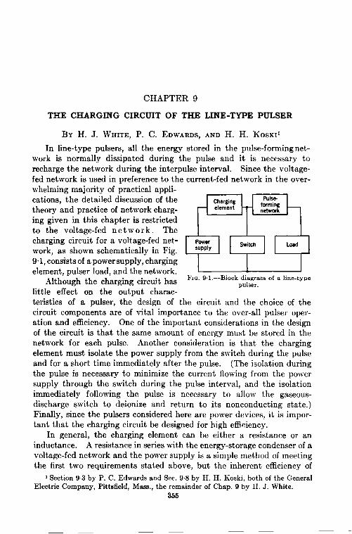
CHAPTER 9
THE CHARGING CIRCUIT OF THE LINE-TYPE PULSER
BY H. J. WHITE, P. C. EDWARDS, AND H. H. KOSKIL
In line-type pulsers, all the energy stored in the pulse-forming net-work is normally dissipated during the pulse and it is necessary torecharge the network during the interpulse interval. Since the voltage-fed network is used in preference to the current-fed network in the over-whelming majority of practical appli-cations, the detailed discussion of thetheory and practice of network charg-ing given in this chapter is restrictedto the voltage-fed network. Thecharging circuit for a voltage-fed net-work, as shown schematically in Fig.9.1, consists of a power supply, chargingelement, pulser load, and the network.
Although the charging circuit haslittle effect on the output charac-
[Powersupply
Switch Load
I
L ‘ IFI~. 9.1.—Biock diagram of a line-type
pulser.
teristics of a pulser, the- design of the circuit and the choice of thecircuit components are of vital importance to the over-all pulser oper-ation and efficiency. One of the important considerations in the designof the circuit is that the same amount of energy must be stored in thenetwork for each pulse. Another consideration is that the chargingelement must isolate the power supply from the switch during the pulseand for a short time immediately after the pulse. (The isolation duringthe pulse is necessary to minimize the current flowing from the powersupply through the switch during the pulse interval, and the isolationimmediately following the pulse is necessary to allow the gaseous-discharge switch to deionize and return to its nonconducting state.)Finally, since the pulsers considered here are power devices, it is impor-tant that the charging circuit be designed for high efficiency.
In general, the charging element can be either a resistance or aninductance. A resistance in series with the energy-storage condenser of avoltage-fed network and the power supply is a simple method of meetingthe first two requirements stated above, but the inherent efficiency of
ISection93 by P. C. Edwardsand Sec. 9.8 by H. H. Koski, both of the GeneralElectricCompany, Pittsfield,Mzm., the remainderof Chap. 9 by H. J. White.
355

356 THE CHARGING CIRCUIT OF THE LINE-TYPE PULSER [SEC. 9.1
such an arrangement is well known to be never greater than 50 per cent.The use of an inductance as the charging element, however, makes itpossible to design the charging circuit for a very high efficiency and toobtain better isolation between the power supply and the switch than ispossible with resistance charging under the same conditions of recurrencefrequency and pulse power. As a result, inductance charging has beenused almost exclusively in pulsers for microwave radar.
The power supply may be either d-c or a-c, depending on the natureof the switch to be used, the pulse power, the recurrence frequency, andthe required flexibility. Since the design of the charging circuit dependson the type of power supply, it is logical to divide the discussion into twoparts: inductance charging from a d-c supply, and inductance chargingfrom an a-c supply.
INDUCTANCE CHARGING FROM A D-C POWER SUPPLY
9.1. General Analysis of D-c Charging.-It is usually possible toanalyze the behavior of the charging circuit by making the followingsimplifying assumptions:
1.
2.
3.
4.
The pulse-forming network is represented by the capacitanceC. appearing between its terminals. The effect of the PFNinductances on the charging voltage wave can be neglected becausethe frequencies involved during the charging cycles are very lowcompared with the natural resonant frequency of the networkmeshes.The pulser switch is assumed to be perfect—that is, its deionizationis assumed to be instantaneous after the discharge of the network-and can be considered as an open circuit.The shunt inductance of a pulse transformer used with a unidirec-tional load has a negligible effect compared with the inductance ofthe charging reactor.The charging reactor is assumed to be linear, that is, its flux isassumed to be proportional to the current. Its inductance musttherefore be constant.
The equivalent charging circuit can then be represented by Fig.9.2 in which the switch S, not present in actual pulsers, is inserted as aschematic means of starting the charging cycle after the discharge ofthe pulse-f orming network. The clifferential equation for this circuit, interms of the instantaneous charge QN on the network, is
(1)
where IL is the resistance of the charging inductor and EU is the power-

SEC, 91] GENERAL ANAL YSIS OF D-C CHARGING 357
supply voltage. If it is assumed that there is an initial current i,(0)in the charging inductance L. and an initial voltage uN(O)across the net-\rork capacitance C~, the initial conditionsimposed on Kq. (1) are: s L,
8
q.(o) = CNUN(0)
I1=Ebb~NL
and
(-)
dq,,(2) l~ro. 9.2.—Equivaleni
dl ,=~= i.(o). charging rircuit for a Iine-tstje
pulser.
With thmc initial conditions, Eq. (1) leads to the following Laplace -transform ctluation:
+i,(0)
— (3)1
P’+;: P+L7N
LetR. 1 1 R:
a = 27,; d = ~v; “ = “; – a’ = L.CN 4L:.
“1’hcn Jhl. (3) becomes
[q..(p) = 6’.vh’bb 1– (p+a)+a
1(p+a)+a
+ q.~r(()) ~ + a)2 + ~Zp (P+a)’+a’
1+ i.(o) (p + a)2 + u’
anfl the corresponding time function can be obtained by inverse trans-formation from tables of Laplace-transforrn pairs. For the oscillatorycmc, which is the only one of interest here, the time function is
‘N(’)‘CNE+-C-”’(cosu’+:sinw’)l+ qh.(o)e-”’
( )
sin dcos d + g sin d + ic(0)e–~( — (4)
(.Ll u
The expression for the network voltage follo!vs immediately.
1+it(0) sin ~t .
C.,w ‘(5)

358 THE CHARGING CIRCUIT OF THE LINE-TYPE PULSER [SEC. 9.1
By differentiating Eq. (4) and simplifying, the expression for currentbecomes
(
E,~ – v~(0) sin di.(t) = e–”t
L. [ 11+ i,(0) cos d – ~ sin at . (6)
u
As stated before, it is necessary that the pulse-forming network becharged to the same potential each time the discharge switch closes if allthe output pulses are to be of the same amplitude. Examination of Eq.(5) indicates that, if this condition is met, and if the charging period isthe same before all pulses and equal to the recurrence period T,, the initialconditions, ON(O)and L(O), must be the same for each cycle. The valueof o.v(0) depends on the load characteristics and is usually constant, exceptin cases of faulty load behavior discussed in Chap. 10. Because of theshort pulse durations that are involved, the current in the inductance atthe beginning of a charging cycle can be considered equal to that at theend of the preceding charging cycle. Then, i.(0) = L(l’’,). From Eq. (6),
[Ebb – ?JN(())Sin uT,
i,(0) = i.(T,) = e–aT’L, u
( )1+ i.(0) cos uT, – ~ sin uT,
Solving,EM – uN(O) sin LIT,
i.(o) = L@ (7)e“” + ~ sin uT, – cos uT,’
and the following general expression for network voltage tiN(t)is obtainedby substituting Eq. (7) into Eq. (5):
k sin cd sin COT,OM(t) = EM + [Ebb – VN(())]C–’”
)r“T’ — cos wT. + ~ sin uT, LCCNW2
The value of network voltage at the time of discharge is given by
LJN(T.)= Ebb + [EM – u,N(0)]e–OT’
k
sin2 uT,
)e“Tr— cos uT. + ~ sin uT, L@,VW2
( )1coswT, + ~ sin uT, . (9)
w
By substituting Eq. (7) in Eq. (6) in the same way a general expressionfor the current that charges the network is obtained, that is,

SEC. 9.1] GENERAL ANAL YSIS OF D-C CHARGING 359
EW – uiv(0) ~_~, e“” sin UL+ sin u(l’, – t).i.(t) =
LN(lo)
co”’ + ~ sin 02’, – cos uT,
If the resistance R, can be neglected, that is, if there are no circuitlosses, a = O, the expressions (8) and (10) for voltage and current maybe simplified to
sin 2t – T,
2 4L.CNv,v(t) = Em + [EM – vjv(0)]
T,
“n 2 ~N
(11)
and
(12)
(Equations (11) and (12) are not valid if T,/2 m; = mr.)The network voltage at the time of discharge given by Eq. (9) reduces to
ZJN(T,) = 2Ebb – UN(O). (13)
In the case of a lossless circuit, the sum of the initial and final networkvoltages is always equal to 2Ew, regardless of the value of the inductancechosen. Practical circuits always have losses, however, but if the “ qual-ity factor, ” Q, of the charging circuit is kept high—10 or more—the ratioof network to power-supply voltage is only slightly less than two, and isnot greatly affected by the actual value of inductance that is used.
As a check on the previous computations, it is easy to arrive at Eq.(13) by very simple physical considerations. Again consider the circuitof Fig. 9.2, and assume R. = O and an initial voltage v~(0) on the net-work. Assume that the energy stored in the induct ante is the same atthe end as at the beginning of the charging cycle, and that a charge q.has been transferred from the battery to the network, resulting in avoltage vN(T,). Then, to satisfy the law of conservation of energy,
qdh = $ {[v,v(T,)]2 – [VN(0)]2) .
But the electric chargeq. = (7N[vN(T,) – v.(O)].
Hence,
qr@ba = ; [o.v(T,) + VN(0)])
oruN(T,) = 2Ebb – UN(O). (13)

360 THE CHARGING CIRCUIT OF THE LINE-TYPE PULSER [SEC.9.1
Equation (7) indicates that the initial current in the inductance L(O)may be either positive, zero, or negative, depending on the relative valuesof both the natural resonant period, (27r/w), of the circuit and the pulserecurrence period. The special case where L(O) = O is called “resonantcharging, ” and corresponds to the first zero of sin ~T, as the argumentincreases, obtained when
uT~ = T. (14)
For resonant charging, the expressions (5) and (6) for voltage and currentmay be simplified to
[~N(t) = EM + e–”~ [U,V(0) — Ebb]Cosd + : Sin d
1(15)
and
giving a network voltage at the time of discharge
VN(~,)= Ebb + [ELJ— ~N(o)]e–aT’.
(16)
(17a)
This equation can be rewritten as a function of the quality factor of thecircuit. Since
Q+, R.
a = 2Z’and aT, = —J
e 2;
the network voltage at the time of discharge is given by
oN(T,) = EM + [Ebb – ~X(0)]e 2;. (171))
It is evident from Eq. (15) that the rate of change of the charging voltageis small in the region of the maximum value. Hence, there are severaladvantages in operating near resonant charging, namely, small variationin output power even if the time jitter in the switch is large, no overvolt-ing when the switch misfires, and a slow buildup of the voltage after thepulse, allowing a maximum length of time for the switch to deionize.The value of inductance corresponding to resonant charging is readilyobtained from Eq. (14), and can be expressed, if the effect of the resist-ance is neglected, by
Since the resonant frequency of the circuit is given by
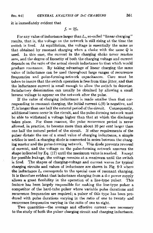
SEC. 9.1] GENERAL ANALYSIS OF D-C CHARGING 361
it is immediately evident that
j, = 2fo.
For any value of inductance larger than L,, so-called “linear charging”results, that is, the voltage on the network is still rising at the time theswitch is fired. At equilibrium, the voltage is essentially the same asthat obtained by resonant charging when a choke with the same Q isused. In this case, the current in the charging choke never reacheszero, and the degree of linearity of both the charging voltage and currentdepends on the ratio of the actual circuit inductance to that which wouldproduce resonance. By taking advantage of linear charging the samevalue of inductance can be used throughout large ranges of recurrencefrequencies and pulse-forming-network capacitances. Care must betaken to insure that the switch operation is free from time jitter, and thatthe inductance current is small enough to allow the switch to deionize.Satisfactory deionization can usually be obtained by allowing a smallinverse voltage to appear on the network after the pulse.
If the value of charging inductance is made smaller than that cor-responding to resonant charging, the initial current i.(0) is negative, andT, is longer than one half the natural period of the circuit. Consequently,additional losses occur in the circuit, and the pulse-forming network mustbe able to withstand a voltage higher than that at which the dischargetakes place. For these reasons, the pulse recurrence period is neverallowed, in practice, to become more than about 10 per cent larger thanone half the natural period of the circuit. If other requirements of thepulser dictate the use of a small value of charging inductance, a simpleartifice is used: a charging diode is connected in series between the charg-ing reactor and the pulse-forming network. This diode prevents reversalof current, and the, voltage on the pulse-forming network assumes theshape indicated by Eq. (17) until the maximum value is reached. Exceptfor possible leakage, the voltage remains at a maximum until the switchis fired. The shapes of charging-voltage and current waves for typicalcharging circuits and values of inductance are shown in Fig. 9.3 wherethe inductance L, corresponds to the special case of resonant charging.It is therefore evident that inductance charging from a d-c power supplyallows a great flexibility in the operation of a line-type pulser. Thisfeature has been largely responsible for making the line-type pulser acompetitor of the hard-tube pulser where variable pulse durations andrecurrence frequencies are required; a pulser of this type has been pro-duced with pulse durations varying in the ratio of one to twenty andrecurrence frequencies varying in the ratio of one to eight.
Two quantities—the average and effective current—are necessaryto the study of both the pulser charging circuit and charging inductance.

362 THE CHARGING CIRCUIT OF THE LINE-TYPE PULSER [SEC. 9.1
They can be obtained by integration over the charging period, using thewell-known relations
/I*V = ; ~=’ i,(t) (-U,
,
and
1:= . L/
T, ~T’ [L(t)]’ Czt.
It is easier, however, to obtain the average current by considering the
2
1
0
0 1 2t/Tr _
4
2
0
-2
0 1’ 2t/Tr —
(a)
2
1
0
EEElo 1 2
t/Tr _
2
1
0
EElao 1 2
4
$11%1
2
0
1 20 1 2t /Ty — t/Tr _
(b) (c)Fx~. 9.3.—Charging~v0ltsge and current wave shapes. UN(0) = O, IL = O, (a) L. = &
(b) Le. = L, (c) L.= 4L. The dottedlinescorrespondto the useof a chargingdiode.
charge on the network, thus
1=, = * = j’,cN[lh.(Tr) – UN(O)]. (18)r
The expression for the effective value of the current is sufficiently accu-rate for most purposes if losses are neglected. The current i,(t) is givenby Eq. (12); therefore,

SEC. 9.1] GENERAL ANALYSIS OF D-C CHARGING 363
I:rm = ;
/
~, [Ew – UN(O)]’ co,, (T, – 2t) ~t
r L T,2 sinz _ 2 4LeCN
O CN 2 dLCCN
= [E,, – VN(0)]’
(
~ + ~L,CN sin T,T, )
— .
2 k sinz —T, m. ’19)
c. 2 4L,CN
The ratio of Z~_ to I-,, obtained from Eqs. (19), (18), and (13)1 isknown as the “form factor,” that is,
~+tiLZN. ~I -— — “n 4L.CN.T,
J ., & T,(20)
2 sin _2 4L.CN
For the special case of resonant charging, where T,/4L.CN = m, theform factor reduces to 7r/2 a = 1.11, the expected value for a sinewave. As the charging inductance increases, the form factor decreasesand approaches unity, as is to be expected since the current approachesa constant value as the value of the inductance approaches infinity.
The efficiency of inductance charging can be readily obtained asthe ratio of the energy supplied to the network during the charging cycleto the energy taken from the power supPlY during the same period. Thus
Substituting I-, from Eq. (18) and simplifying,
~c= ON(T,) + VN(0)
2EN(21)
For the case of resonant charging, VN(T,) is given by Eq. (17b) and Eq.(21) may be simplified to
~,=l+e-~ UN(O)1 — e-a2 ‘Eti2= ‘ -fi(l - %?) ’22)
In many cases, oN(O) is equal to zero, and the charging efficiency is givensimply by
(22a)
It is seen that the efficiency varies from about 92 to 96 per cent values ofQ ranging from 10 to 20, whereas for resistance charging the efficiency isonly 50 per cent.

364 THE CHARGING CIRCUIT OF THE LINE-TYPE PULSER l~EC. 9.2
9.2. Practical D-c Charging Reactors.—The approximate ranges ofvalues of inductance, average-current, peak-voltage, and recurrence-frequency requirements for the majority of d-c charging reactors used inmicrowave-radar applications are as follows:
Inductance 1 to 100 henrysAverage Current 0.01 to 1.0 ampPeak Voltage 1 to 30 kvPulse Recurrence Frequency 200 to 4000 pps
The inductance and current requirements are such that it is nearlyalways advantageous to use iron-core inductors. Because of the highnetwork voltages encountered and the surge voltage that appears betweenturns at the high-voltage end when the switch is closed, very carefulinsulating and processing of the units are required. Oil impregnationwith hermetic sealing is used almost entirely for voltages higher thanabout 5 kv.
Linearity Requirements jor D-c Charging Reactors.—In the theoreticaltreatment of d-c inductance charging, a linear reactor of constant induct-ance is assumed. Linear, or approximately linear, inductors are also themost satisfactory in practice. As anticipated from physical considera-tions, small departures from linearity affect the results only slightly.Large variations in the charging inductance produced by saturation of theiron core are usually not permissible because of the excessive power loss andthe possibility of operating in a region of nonrepeating charging voltage.
In the theoretical discussion of d-c charging it is shown that, whenusing a linear charging choke, repeating transients may occur under all
conditions. The proof is not valid when the
- r
inductance varies with the current or, morespecifically, when the total magnetic flux in thereactor is not proportional to the current. For
ta nonlinear reactor, the differential equation for
% the charging current must be written in the form
~, ‘~ + Rw~ +&N/
& dt = EM, (21)
~~o i~—
where Nc is the number of turns on the reac-
FIQ. 9.4.—F1ux& as a tor and ~. is the total flux, which is assumedfunction of current.G for a to be confined to the core. The total flux @.chargingreactor. is a function of the charging current, +. = @(i.),which may be found by experiment and has the form shown in Fig. 9.4.Equation (21) may then be solved graphically or numerically for L(t). Itshould be noted, however, that this method of solution does not provethat the repeating transients required for stable d-c charging exist.

SEC. ’32] PRACTICAL D-C CHARGING REACTORS 365
At currents sufficiently below saturation, +. = L% and the reactorbecomes approximately linear. As the core becomes saturated, the
d+.incrcrnchta] inductance N.X, becomes very small, and large increases
cin current are necessary to maintain a given voltage across the reactor.AS a result high peak currents occur in thereactorwben d-c chargingsused.
Experimental charging-current and voltage waveforms for a typicalnonlinear reactor are shonmin Fig. 9.5. At Z,mT= 44 ma, the charging-current waveshapes are the same as those to be expected from a linear,choke. At 50 ma, their loops have become quite peaked, indicating the
(a) I,ew = 44 ma; (b) I,av = 50 ma: (c) Ic~v = 52 ma.FIG, 9,5.—D-c charging current and network voltage obtai,led from nonlinear charging
reactor.
onset of saturation. Finally at 52-ma average current, the loops nolonger repeat from cycle to cycle, but rather repeat in alternate cycles,one cycle having a much higher peak current and condenser voltage thanthe other. Thk occurrence indicates a high degree of saturation and,of course, is not permissible in practice. A general explanation follows.
At low average currents there is no flux saturation of the iron core,and the charging waves are those for a linear reactor. As the average ordirect current is raised, a point is reached where the reactor starts tobecome saturated at the current peaks. This saturation lowers theincremental inductance, which in turn increases the peak current. Theeffect tends to be regenerative and somewhat unstable, and causesthe current peaks to increase rapidly in amplitude as the direct current israised. At the same time, the period of the L.C M-circuit decreases, caus-

366 THE CHARGING GIW’UZZ’ OF THE LINE-TYPE PULSER [SEC. 9.2
ing the charging voltage to overshoot and the charging current to becomenegative before the switch is fired. As a result, the reactor inductanceremains high for a longer period on the following cycle, and the current isthereby prevented from reaching the high peak value of the precedingcycle. Since a higher inductance also means a longer charging period,the reagtor current still has a positive value at the instant when the net-work discharges. Saturation is encouraged by this positive value of theinitial current, and the high and low current loops are repeated alternatelyin a perfectly stable manner. The whole phenomenon occurs becausethe reactor has a relatively high average inductance on one cycle and arelatively low average inductance on the following cycle.
‘ The failure to obtain cycle-to-cycle repeating transients is a goodillustration of the statement made earlier that repeating transients mayor may not be obtained in any case, and that the proof of their existenceis limited to linear reactors. Linearity is therefore important in thedesign of charging reactors for pulsers; however, its advantages have tobe iveighed against its cost.
It is possible to make charging reactors with any desired degree oflinearity, but, in general, they are larger and heavier, the stricter thelinearity requirement. Thus, for use in airborne sets, they are usuallymade somewhat nonlinear in order to save weight and size. When weightis not an important factor, the majority of charging reactors for pulsersdesigned at the Radiation Laboratory satisfy the following conditions forlinearity and inductance variations.
1. Lhearit y. The inductance shall not change by more than 5 percent measured at rated full-load and at half the rated full-loaddirect current.
2. Inductance value. The inductance shall be within the tolerancerange of from +6 to —2 per cent of the design value.
Charging reactors for airborne applications are usually specified onthe basis of samples that are tested in an electrical model of the pulserunit. Reactors having varying degrees of nonlinearity are tried until asatisfactory compromise is obtained between linearity and heating onthe one hand and weight and size on the other hand. This method ofdesign is justified on the basis of the large amount of adjustment necessaryfor airborne sets, and of the very large numbers in which these sets usuallyare made.
Inductance Measurements. -Inductance-measuring circuits are de-signed to simulate the current wave shapes for d-c resonant charging,which consist .of a series of half sine-wave loops. Such a current can beobtained exactly by using a line-type pulser of adequate voltage andcurrent capacities, but thk method is very awkward, inconvenient,

SEC. 9.2] PRACTICAL D-C CHARGING REACTORS 367
and expensive. Thevoltage and current wave shapes can be simulatedby the output of afull-wave rectifier consisting of an LR-circuit of theproper ratio. i This method, on the other hand, is rather slow and inac-curate because it involves adjustment of the resistance until the wave
TransformerJZF=15h ~.
R,
11~5M
r
T:;I
1-20 J_=Fm. 9.6.—Circuitfor meaauringtheinductanceof a chargingreactor.
becomes tangent to the zero axis on an oscilloscope. Hence, the simulat-ing circuit shown in Fig. 9.6 has been used in preference to both the pre-vious methods, and its explanation follows.
Superimposed direct and 6fl-cycle alternating currents are passedthrough the reactor L. under test, the alternating current being suppliedby means of a transformer and the direct current by means of a d-c powersupply to which an additional filter section CFLF has been added. Thecapacitance C provides a very low impedance path for alternating cur-rents, and an accurate measurement of the alternating component ofthe current may be obtained by inserting an accurate a-c milliammeter inseries with C.
In operation, the direct current is adjusted to the desired value andthe alternating current is then ad-j usted so as to have a peak valueequal to the direct current. Forthis condition, assuming a per-fectly linear reactor and a purelysinusoidal voltage, the currentwave becomes tangent to the zeroaxis and rises to a peak value equalto twice the direct current, as illus-trated in Fig. 9.7.
21cav
&av
o21r 4U
coat—FIW 9.7.—Current through the chargingreactor in the inductsnca-measuringcircuit.
The magnitude of the alternating current to be used is calculatedfrom the relation
I‘“” = %
(22)
1A. C. Donovan, “The Mezaurementand Design of D-C Rezonant ChargingChokes,” RL Report No. 51-14, NOV.23, 1942.

368 THE CHARGING CIRCUIT OF THE LINE-TYPE PULSER [SEC. 9.2
The value of L, is given by
L. = >,.
(23)
where the applied angular frequency 00 = 377 for 60-cycle voltage. Theuse of 60-cycle voltage is preferred because both the frequency and waveshape supplied by the public utilities usually are accurately controlled,and also because 60-cycle frequency allows the use of relatively low alter-nating voltages to obtain the necessary (and sometimes high) values ofalternating current. The meters used should be accurate to 1 per cnntor better in order to obtain suitable accuracy for the inductance L=.
The ratio of peak to average current for the wave of Fig. 9.7 is 2/1,whereas the ratio obtained in the pulser circuit for a linear reactor andresonant charging is 7r/2 = 1.57. The test circuit therefore imposes ahigher peak current in the reactor than it will carry in actual service.The increase, which is by a factor of 4/m = 1.27 for d-c resonant charging,may be regarded as a safety factor in the measurement. The factor isgreater for linear charging, approaching the value 2 in the limit. Advan-tage may sometimes be taken of the decreased peak current occurring forlinear charging in order to decrease the size of the reactor core.
When L. is nonlinear, the method of measurement outlined abovegives an approximate average value for L. over the current range that isused. This value is satisfactory for checking inductors against thelinearity and inductance conditions given in the preceding section.
The inductance-measuring equipment usually incorporates an oscil-Ioscopic viewing system for directly observing the B-H curve for thereactor under test. In Fig. 96 these added elements consist of theresistor Rl, the resistor and condenser R 1 and Cl, and the oscilloscope.The voltage across Rz at each instant is proportional to the magnetizingforce of the reactor, since
and is applied to the horizontal deflecting plates. The voltage across Cl,which is applied to the vertical deflecting plates, is proportional to theflux density, as is shown by the following calculations. Neglecting thevoltage drop across the react or resistance, the voltage across R lC 1 isgiven by
N,A dB.v&=?!&??=—108 z’
where A is the cross-sectional area of the core. If the values of RI andC, are chosen so that the current in that circuit is determined almost

SEC. 9.2] PRACTICAL D-C CHARGING REACTORS
exclusively by the resistance, the voltage across C 1is given by
369
The degree of linearity of a charging reactor is probably best shownby means of oscillograms. For an ideal perfectly linear reactor havingno losses, the B-H oscillogram consists simply of two straight linesenclosing zero area. The B-H oscillogram for a well-designed iron-core
(a) I.,V = 0.050 (b) Z.mv = 0.100 amp, (c) I~mv= 0.125 amp,amp,
L, = 31.6 JZ. = 2S. 1 henrye. L. = 22.5 henrys.henrys.
IeJIeaV = 0.70
(d) I.mv = 0.150 amp,
L. = 18.8 henrys.
(e) I.,w = 0.050 (j) I=., = 0.100amp, (g) 1.., = 0.125 amp, (h) ICav = 0.150 amp,amp,
L. = 31.1 L. = 28.0 henrys, L. = 25.9 henrys, L. = 22.5 henrys.henrys,
IcJI,..V = 0.40.
(*-) L,v = 0,100 ~) I.mv = 0.125 amp, (k) Iemv = 0.17’5 amp, (2) I.., = 0.200 *mP,amp,
L. = 29.0 L, - 26,5 henrys. L. = 23.9 henrys. L. = 19.2 henrys.henrys.
l<*.e/I.m” = 0.10.
FICJ.98.-B-H oscillograms for a typical d-c charging reactor rated at I.nv = 0.10 amp,B is vertical and H is horizontal.

370 THE CHARGING CIRCUIT OF THE LINE-TYPE PULSER [SEC. 9.2
reactor departs only slightly from the ideal case as it consists of twoslightly bowed lines that form a narrow B-H loop of small area. A goodexample of such a B-H loop for a reactor tested at half-rated direct cur-
(a) I.,V = 0.050 (b) Icav = 0.100 amp, (c) 1.., = 0.150 amp. (d) I%V = 0.200 amp,
amp,L. = 30.3 L. = 29.1 henrys. L, = 22.7 henrys.
henrys.L. = 15.6 henrys.
Ik=/Ie,, = 0.70.
(e) I.bv = 0.050 (f) I..* = 0.100 amp, (p) I.av = 0.150 amp, (h) 1%, = 0.200 amp,amp,
L. = 30.0 L. = 29.9 henrys. L. = 26.5 henrys. L. = 16.2 henrys.henrys.
La-of1.,7 = 0.40.
(a) 1.., = 0.150 (j> 1.., = 0.260 amp, (k) Z.av = 0.250 amp, (t) Z,-, = 0.300 amp,amp,
L. = 27.1 L, = 20.9 henrys. L. = 10.6 henrys. L. = 7.1 henrys.henrys.
IcJI,av = 0.10.
Fm. 9.9.—B-H oacillograme for a typical d-c charging reactor rated at 1%, = 0.19amp, B is vertical and H is horizontal.
rent is shown in Fig. 9.8a. The onset of saturation of the reactor corewhen the direct current is increased to the rated value is shown in Fig.9.8b. Further increases in the current produce core saturation over agreater range of the B-H loop (Fig. 9“& and 9JM.)

SEC. 9.2] PRACTICAL D-C CHARGING REACTORS 371
The saturated portion of the loop has a slope that is characteristic ofthe inductance of the equivalent air-core reactor. For example, in Fig.9.8d the relative slope of the steep to the flat portion of the B-H loopis about 20/1, which indicates that the inductance is increased by afactor of about 20 when the air core is replaced by an iron core of the samesize. The corresponding ratio for the curve of Fig. 9.9d for anotherreactor is about the same.
The oscillograms in Fig. 9.8 are all for the same reactor, but are takenfor different values of the current ratio l,W/lC~Y, the ratios being 0.70 forFig. 9.8d, 0.40 for Fig. 9.8e-h and 0.10 for Fig. 9%-1. The lC~c/lCsVcurrent ratio of 0.70 corresponds to the test condition, the ratio of 0.40 tosine-wave or d-c resonant charging, and the ratio of 0.10 to nearly linearcharging. In the case of linear charging, it should be noted that the B-H
loops for large direct currents (Figs. 9.8k and 1) do not show the two-slopecharacter, but rather are relatively linear. This linearity is a character-istic of the B-H loops that is to be expected when the component ofalternating current is relatively small. 1
The oscillograms of Fig. 9.9 are similar to those of Fig. 9.8, but arefor a reactor of somewhat different design. The latter reactor is definitelynonlinear when operated at its rated current of 0.190 amp. In a pulsercircuit it will therefore give rise to a charging wave of the same generalcharacter as that previously shown in Fig. 9.5. It is therefore unsuitableas a d-c resonant-charging reactor for a current of 0.190 amp, althoughfor currents of 0.100 amp, or possibly 0.125 amp, it would be satisfactory.
40 40,
g
.E .s
Q“ 10 4“ 10 - >
0 00 50 100 150200 0 50 100 150 200 250 30LI
Xc~v in ma 16~v in ma
(a) (b)
Fm. 9.10.—Inductanceas a functionof currentfor iron-cored-c chargingreactors,(a)Linearreactor(seeFig. 9%), (b) nonlinear reactor (see Fig. 9.9).
The B-H oscillograms thus serve as a rapid and rather sensitive visualtest of the linearity of a reactor and of its suitability as a charging choke;however, they should always be supplemented by meter measurements in
1For a discussionof themagneticcharacteristicsof ironnnderthesecircumstances,sss Membersof the Sta5 of the Departmentof ElectricalEngineering,MassachusettsInstituteof Technology, Magnetic Circaifsand Transformers, Wiley, New York, 194.3,pp. 197-202.

372 THE CHARGING CIRCUIT OF THE LINE-TYPE PULSER [SEC. 9.3
order to determine the numerical value of the inductance. Figure 9.10shows the results of such measurements for the same two reactors.
The inductance of d-c charging reactors can also be measured bya power bridge. 1 The voltage supplied to the bridge circuit is obtained bythe addition of a-c and d-c voltages in such a way that the peak alternat-ing current is equal to the direct current. Inductance and quality-factor measurements made with the power bridge can be accurate to
%ction A-AFIG. 9.1 1.—Sketch of
d-e resonant-charging re-actor.
within ~ and 1 per cent respectively.9.3 The Design of D-c Charging Reactors2.
Figures 9.11 and 9.12 show the usual form of thed-c resonant-charging reactor. The essentialelements of a complete reactor are the coil, thecore, the air gap in the core, and the enclosingcase. Accuracy in both design and manufactureis necessary to obtain reactor characteristicsthat are within specified limits.
Core Design.-The degree of linearity of theinductance is determined by the relationship be-tween the characteristics of the core material andthose of the air gap. The following limits, how-ever, have been found to apply generally to coresteels:
1. Maximum flux density in the core = 55kilolines/in2.
2. Ratio of the air-gap spacing to the meanlength of the magnetic path 2 0.6 per cent.
If the current density in the copper and the flux density in the coreare held constant, a larger gap requires a greater number of turns in thecoil and a smaller cross section for the core in order to produce a giveninductance. Thus, as long as the above limits are met, the designer hasthe freedom to reduce the weight of either the copper or the iron. Theratio of copper to iron in the reactor is important from the standpoint oflow cost and high operating efficiency.
Laminations 0.014 in. thick can be operated at frequencies up to 600cycles/see, but for frequencies up to 15 kc/see the thickness should notexceed 0.005 in. For any given operating frequency and steel thicknessthe designer can control the core loss by varying the peak operating fluxdensity. The operating frequency to be used in the design is the resonantfrequency of the charging circuit of the pulser.
Cod Design. -Coils for resonant-charging reactors as well as for a-c
1Standard Handbook jor Electrical Engineers, 7th cd., hIcGraw-Hill, New York,1941,pp. 1s0-1s5.
2By P. C. Edwardsof the GeneralElectric Company, Pittsfield, hlaee.

Sllc. 9.3] THE DESIGN OF D-C CHARGING REACTORS 373
resonant-charging transformers (see Sec. 9.8) must withstand continuedelectrical impulses, as the voltage across the coil reverses in polarityin a few microseconds when the pulser switch closes. This condition isconsiderably more severe than that to which normal reactors and trans-formers are subjected.
The distributed capacitance that occurs between the coil turns andthe winding layers has several effects upon the circuit: it increases thelosses by the dissipation of the stored energy, ~C,V\, at the time theswitch closes; it tends to detune the charging circuit, an effect which issmall except for very short pulses; in the case of d-c charging, it causessome impulse voltage to be applied to the rectifier circuit; and, during
Fxri. 9. 12.—Core-8nd-coti aeeembly of a resonantiharging reactor. (Courte.sv of GeneralElerttic Co.)
the discharge of the pulse-forming network, it produces an uneven voltagedistribution throughout the coil, thus placing an undue stress on certainparts of the coil conductor and layer insulation.
The distribution of impulse voltage can be improved by designing acoil so that the radial build is about i to f the length of the coil windinglaYer. This ratio is a compromise between that needed for good impulse-voltage distribution and that for a low coil capacitance. As the ratio of
the coil dimensions decreases the voltage distribution improves, but thecapacitance becomes greater. It is possible to control the distributionof impulse voltage by means of an electrostatic shield that is applied overthe finish layer of the coil and connected to the output lead, as shown inFig. 9.11. This shield can be either a metallic wire screen or a conductoron the last layer of the coil.
Methods oj Treating, Tanking, and Sealing.—In addition to the mag-netic and electrical design requirements outlined above, the reactors and

374 THE CHARGING CIRCUIT OF THE LINE-TYPE PULSER @~c. 9.3
transformers developed for radar applications have to meet generalspecifications for humidity and temperature, acceleration, insulation,mechanical handling, and life. Accordhgly, the higher-voltage units areusually built in hermetically sealed tanks, and special techniques ofhandling oil expansion, vacuum treatment, insulation, and heating areused.
Varnished units are used whenever conditions of ambient temperatureand humidity are not severe, voltages are not high, and low cost andlight weight are of prime importance; new types of dry insulation recentlydeveloped have shown great promise up to 10 to 15 kv (see Sec. 14.3).
When the reactor is enclosed in a hermetically sealed case, some typeof filling compound or oil is required to aid in the process of cooling thecore and coils, and to provide the necessary insulation between the coiland grounded parts. When used with vacuum-treating technique, oilhas the advantage over the compounds now available in that it is able tofill all voids and remain free from cracks at normal operating tempera-tures. Since the initial corona discharge that is usually the starting pointfor insulation failure is often associated with air pockets and voids in theinsulation (see Sec. 6.5), the flow of oil into the vicinity of the sparkimmediately after the internal flashover helps to prevent recurrence ofsuch a breakdown, and the solid insulation does not become carbonized.
When used with a hermetically sealed case, oil provides a durable,reliable, and long-lasting insulation, even at continuous operating tem-peratures as high as 115”C. Compounds provide an inexpensive, thoughnot so reliable, filling medium for high-voltage units. The decisionwhether to use oil or compound is usually made on the basis of theapplied voltage and reliability desired.
Practical values usually accepted as the maximum allowable voltagegradients for a satisfactory reactor and transformer are listed in Table9.1.
TABLE 9.1.—MAxxMuF.I ALLOWABLE VOLTAGE GRADIENTS
Working streaa,Quantity peak volts/roil
Solid insulationcoil to ground 100Scdidlayer insulation 100No. 1O-Ctransformeroil 75Surfacecreepfrom coil to ground 20Surfacecreep insidecoil 20
Representative charging reactors are shown in Fig. 913, and Table9.2 gives their significant design values.
Heating—The reactor losses produce heat in the core and coil.Excessive coil temperatures not only damage conductors, but also causedeterioration of the usual organic insulating materials.

SEC. 9.3] THE DESIGN OF D-C CHARGING REACTORS 375
Oil expansion and contraction give rise to forces on the sides of thetank, which may result in mechanical damage to the seams. Severalmethods have been used to limit the pressure built up in the tank.
1. The amount of expansion can be reduced by the use of sand to dis-place part of the oil, and the pressure may sometimes be limited toa practical value by combining this method with a flexible tank.
2. An air space at the top of the tank has been used to limit the pres-sure by compression of the air.
FIG. 9.13.—Repressntative d-c charging reactors.
3. Various mechanical expansion chambers have been used which
reduce the pressure to its lowest possible value. The most satis-
factory mechanical device is the metal bellows provided that the
resultant increase in case size can be tolerated. An empirical
equation for calculating the final oil temperature and pressure for
a given design is given in Sec. 9.8.
TABLE 9.2.-SIGNIFICANT DESIGN INFORMATION FOR REACTORS OF FIG. 9.13
No.
ab
c
d
Type ofservice
AirborneGround orship
Ground orship
Ground orship
Weight,lb
5:11~
45
71+
Over-allheight, in.
D-c currentrating,amp
0,0500.100
0.200
0.400
Peakvolt-age rating,
kv
88
17
17
Lrating,henrys
9824
28
19
Z’esting-A preliminary test is conducted prior to sealing the core-and-coil assembly into the case in order to insure that, as far as possible,

376 THE CHARGING CIRCUIT OF THE LINE-TYPE PULSER &C. 9.3
the final sealed unit will meet the inductance specifications, and thus toavoid the necessity of opening the case to adjust the reactor. A finaltest is also made in order to determine whether or not the reactor insula-tion has been damaged, the inductance and d-c resistance have changed,or the power loss or Q factor have varied excessively during the processing.A 1 per cent change in inductance can result from the treating process,which apparently modifies the gap spacing in the core slightly.
The insulation tests consist of an applied-voltage test and an induced-voltage test. In the applied-voltage test, which is used to check themajor insulation of the reactor, a 60-cycle voltage, the rms value of whichis
4?lzab + 1000
W’
is applied for one minute between ground and the two short-circuitedreactor terminals. The induced-voltage test, in which the voltage isapplied between the reactor terminals, checks the insulation between theturns and layers of the coil. In standard practice, the test duration is7200 cycles, and the rms value of the induced voltage is 1.5~0Ew,/@
L_.._-_!–– ._._---JFIG. 9.14.—F&actor core formed of pre-
cut strip steel. (Cotirted~ of GeneralElecfric Co.)
The test is made at frequencies from400 to 800 cycles/see, dependingupon the equipment available.
A comparison of the preliminaryand final values of either the powerloss or the quality factor indicateswhether or not the unit has passedthe induced-voltage test. Thischange is usually not over 5 percent. Turn-to-turn failure in thecoil is readily distinguished by anincrease in power loss or decreasein Q, whereas the measured induct-ance does not change appreciably,esDeciallv when the number of
turns involved in the failure is small co”mpared with the total number ofcoil turns.
Finally, the d-c resistance of the coil is measured in order to makecertain that the coil conductor is continuous and that the coil containsabout the proper number of turns of the specified wire size.
Sample Design.—The followitig sample calculations demonstrate twogeneral design procedures. Figure 9.14 shows the core and Fig. 9.12shows the core-and-coil assembly in the mounting clamps. The specifica-tions applying to this unit are
SEC. 93] THE DESIGN OF D-C CHARGING REACTORS 377
D-c power-supply voltage: 13 kv.Inductance andtolerance: 7.4 henrys, –2to+6per centatfu11-load
current and less than 5 per cent variation from 50 per cent to full-load current.
Average charging current: 0.274 amp. . Ratio of rms current toaverage current = 1.11.
Recurrence frequency: 1170 pps.Core frequency: 585 cycles/see.Peak-charging-wave voltage on pulse-forming network: 25 kv.Allowable minimum quality factor at rated core frequency: 25.Ambient temperature range: 0° to +60”C.Resonant charging.Bidirectional switch (triggered gap).Matched pulse load, that is, UN(O)= O.
Reactor design is usually based on experience. However, in theabsence of suitable previous experience the design process can be startedmathematically.’ If the ratio of air-gap length to magnetic-path lengthis 0.6 per cent or more, and the flux change is large compared with thed-c flux, the energy stored per unit volume of core maybe equated to themagnetizing force and flux density in the core steel, that is,
whereL,. =
I -k .
v=
lm =
A,. =
BF. =
and
(NJ-,) =lm
Note that
that portion of the inductance of the reactor associatedwith the flux in the core steel (the flux that threads thecoil turns but does not flow through the complete lengthof the core is disregarded in the initial design calculation),peak rated amperes flowing in the reactor,core volume in in. 3 = l~A l%,
length of average magnetic path in in.,net cross-sectional area of the steel in in. 2,flux density in core steel in lines/in. 2,
peak ampere-turns/in.
fLF.(I_) 2 is the maximum instantaneous magneticenergy, in watt-seconds, stored in the core. Since about 98 per cent ofthe total number of ampere-turns are required to produce the flux inthe air gap, the energy in the reactor is predominantly associated with this
1C. R. Hama, “ Design of Reactance and TransformersWhich Carry DirectCurrent,” ~. Amer. InAt. Elect. Enws., 46, 128 (1927).
378 THE CHARGING CIRCUIT OF THE LINE-TYPE PULSER [SEC. 9.3
part of the magnetic circuit. For simplicity in the calculation, however,the energy is apportioned to the complete core volume includlng the airgap. For a charging reactor using normal core steels, the value of(N~W)/l~ is approximately 85 when the flux density in the steel is55,000 lines/in.2 and the gap length is 0.6 per cent. This figure isadjusted somewhat to allow for flux-fringing at the air gap. The valueis increased or reduced in inverse proportion to the fringing effect.Using the above figure,
WF.(I*A) 2 = 0023 watt-seconds/in. 3v
of core, includhg the gap.
v
The number of turns canminimum size, the reactorarea of the core window.
Thus, the core volume is
_ ~LF.(Z_)2 in ~—0.023 “
be calculated from Nc y 85 1~/Z.~. Forcoil and insulation should fully utilize the
Experience has shown that about 80-per cent of the total flux thread-ing the coil turns is in the core steel; the remainder is leakage flux.Hence, an approximate value maybe obtained by considering L,. = 0.8LC.
The energy ~L,(l_)z stored in the reactor determines the core sizeand the operating voltage gives an indication of the additional spacerequired for insulation.
Graduated sizes of reactor cores can be designed and tabulated. Thedata required are: core dimensions, net cross-sectional area, weight,volume per unit of stack, length of magnetic path, and the maximumnumber of ampere-turns that can be wound into the window for differentthicknesses of insulation (that is, various voltage levels).
The designer can readily determine core dimensions, coil turns, andinsulation thicknesses by trying two or three cores from the standardlist prepared as above. In the following example, it is assumed that thereactor core and coil sizes have been determined, and that this calculationis the final check on the design. Note that the adjustment in core cross-sectional area and coil turns must be made previously because the amountof leakage flux has been assumed. The actual values must be calculated,and used to determine the inductance.
As a result of the design calculations, the coil is to be constructed of3394 turns. The major portion of the coil conductor is 0.0253 in. DECwire that has a cross section of 0.000503 in. 2 The last layer, shown asthe finish layer in Fig. 9.11, is wound of 6/30 AWG tinned-copper cableinsulated with paper to give an insulation layer thickness of 0.012 in.which adds 0.024 in. to the diameter of the stranded conductor. The

SEC. 9.3] THE DESIGN OF D-C CHARGING REACTORS 379
cable is finished with a 0.007-in. layer of cotton. The resulting dimen-sions for a rectangular coil are:
1; = 2.063 in. w~ = 2.438 in.10 = 5.813 in. w. = 6.188 in.
length of winding layer .L = 2.875 in.
The core, Fig. 9.14, uses 0.014 in. by l+ in. low-loss precut formed steelstrips built up to ~ in. The center leg gross cross-sectional area is thestrip width WZtimes the total buildup hz, or 1.688 in. 2 Assuming a spacefactor of 90 per cent the net steel cross-sectional area, A~., is 1.519 in.z,and the windows for the coil are 4* in. by 2~~ in. The mean length ofthe magnetic circuit 1~ is
1~ = 2(hl + wl) + ~ ri = 15.9 in.
where hl is the height and w, the width of the window, and ~ is thecorner allowance.
If the length of the core gap lais chosen to be 0.114 in.,
1,
K= 0.0072,
and the net area of the air gap, including fringing, is given by
A, = w~h~ + #(h2 + WJIC = 1.89 in.z,
where hz = l~in. and WZ = 13 in.The area of the coil for leakage flux is given by
Al~ = 2WJi + WO1O– A, = 13.5in.Z
3
The ampere-turns in the steel are determined as 20 (rms value) consistingof 1.15 ampere-turns/in. for the steel at 50,000 lines/in. 2, and 1.7 ampere-turns for the core joint. Finally, the design-center voltage across thereactor is obtained from
Va = 2wfoLaIm = 8450 volts,where
*j, = ~ = 585 cycles/see.,
La =
andI -.
/2
design-center inductance, or rated value adjusted to be atthe center of tolerance range = 1.02 X 7.4 = 7.55 henrys,
1.11 X 0.274 = 0.304 amp.

380 THE CHARGING CIRCUIT OF THE LINE-TYPE PULSER [SEC. 9.4
Checks on the design are then obtained by computing the inductanceby either the a-c or the d-c method.
By the a-c method, the voltage across the reactor is obtained from
V. = 4.44@ .N.fO X 10_’ volts,
where +T, the total flux, is the sum of the flux in the core &.. and the leak-age flux f$lk. The total number of ampere-turns (rms value) is
N.J.,= = 3394 X 0.304 = 1032,
of which 20 are in the steel, and 1012 across the gap. Then, the flux inthe gap and steel is given by
4Fe = 4.51$’ 101Z = 76,000 lines,
r$u = 4.51 ~ 1032 = 21,900 lines,w
and1#),= 97,900 lines.
where 4.51 is the permeability of air in lines per square inch per rmsampere-turn per inch from which V. = 8600 volts, which is within themanufacturing tolerance since the design-center voltage is 8450 volts.
By the d-c method, the peak ampere-turns is
NJ,* = ~ 1aS394 = 1460 ampere-turns,
resulting in a total flux of 97,900 lines, which corresponds to an inductance
N.4T 10–8 = 7.7 henrys.L,=rcd
This value again checks closely with the value for the design~enterinductance obtained above.
INDUCTANCE CHARGING FROM AN A-C SOURCE
9.4. General Analysis of A-c Charging.-The energy-storage con-denser of a voltage-fed network may be recharged from an a-c voltagesource whose frequency is integrally related to the recurrence frequencyof the pulse generator. Some intermediate element must be interposedbetween the pulse-forming network and the a-c voltage source; otherwise,it is impossible to discharge the network at a voltage peak and at thesame time retain stable conditions. For example, if the network is con-nected directly to the terminals of an ordinary high-voltage transformerand then discharged at the peak of the transformer voltage, the network

SEC. 9.4] GENERAL ANALYSIS OF A-C CHARGING 381
tends to recharge immediately, and the transformer is short-circuited forthe remainder of the half cycle under consideration.
Perhaps the most obvious means of avoiding this difficulty is to use ahold-off diode between the network and the transformer, and to dischargethe network on the following half cycle, which has a polarity opposite tothat of the charging half cycle. Under these conditions the networkdoes not recharge immediately; consequently, the circuit action is stable,but the utilization factor for the high-voltage transformer and a-c sourceis low (see Sec. 9.9).
The other simple method for recharging the network from an a-csource is to interpose a series inductance between the high-voltagetransformer and the net work. By the proper adjustment of the valueof this inductance, the PFN capacitance, and the voltage phase, thenetwork may he discharged at a voltage peak and stable circuit actionretained. The series inductance also isolates the network from the powersupply for an appreciable time after the pulse, allowing the switch restrik-ing voltage to increase faster than the applied voltage.
The conditior,s for a-c inductance charging are considerably morecomplicated than those for d-c charging, primarily because there are morevariables to consider. These variables include the voltage phase angleat which the network is discharged, and the relation between chargingperiod and impressed frequency. The equations for a-c inductancecharging are therefore more difficult to derive and apply, and a reasonablycomplete study of all the possible variations is lengthy and somewhatcumbersome.
The simplest type of a-c inductance charging (as well as the one mostoften used in practice in this country) is a-c resonant charging, in whichthe charging circuit is tuned to resonance at the impressed a-c frequency.The network voltage reaches a maximum value when the impressedsinusoidal voltage is passing through zero. The pulses therefore occurwhenever the impressed voltage is zero. Although the pulse recurrencefrequency is usually equal to the impressed a-c frequency, it is sometimesdouble the impressed frequency, in which case there is one pulse for eachhalf cycle of the applied-voltage wave. The disadvantage of a-c resonantcharging is that the voltage across the network continues to build up ifthe switch misses one or several pulses. Considerable work on a-ccharging has also been done by the British, who often use nonresonantcharging to alleviate this disadvantage.
A-c inductance charging has the advantage of simplicity, and permitsa net saving in weight and size, particularly since the inductance is usu-ally built into the high-voltage transformer. On the other hand, itgenerally requires a special motor-alternator for each design in order tosupply the proper frequency, with a resultant lack of flexibility. The

382 THE CHARGING CIRCUIT OF THE LINE-TYPE PULSER [SEC. 9.4
disadvantage of requiring a special motor-alternator is offset to a certainextent by the advantage of being able to control the pulser power outputby varying the relatively small field current of the alternator. In con-trast, the power output of a high-voltage d-c rectifier, such as used in d-cinductance charging, must usually be controlled by a large motor-driveninduction regulator or a set of motor-driven variacs, which necessitatesan increase in weight and a more complicated circuit.
A-c charging pulsers having rotary-gap switches are used extensivelywhere relatively high powers and low recurrence frequencies are specified.Rotary spark gaps, however, require self-synchronous triggers and alsointroduce a time jitter of about 25 psec or more. Triggered fixed sparkgaps or thyratrons produce very little time jitter, but, because a more
complicated circuit is needed, they have not
J;:a ‘ngpulsers
been used to any great extent in a-c charg-
The equations for a-c charging require“T the general solution of the series-LRC circuit
I 1 for an applied a-c voltage of arbitra~ fre-FIG,9.15.—Schematic cir. quenc y and phase. The following method of
cuit for a-c inductancecharg-ing.
solution for the circuit of Fig. 9.15 is basedon the use of complex quantities and numbers.
The differential equation for the circuit in terms of the charge q~ onthe network is
(Hereafter, the abbreviation “ Re” meaning “ real part of” is usuallyomitted.) As usual, ~a = Eae~*,so that Eb is the magnitude and q thephase angle of ~a. The bar notation is used in this section to denotecomplex numbers.
By inspection, the particular or steady-state integral of Eq. (51) hasthe form
q](t) = ~NejWof,
where ~~ is determined by substitution in Eq. (51), that is,
The complementary or transient integral is the same as that alreadyfound for the d-c charging circuit, namely,
where ~ is a complex constant of integration and

SEC. 9.4] GENERAL ANALYSIS OF A-C CHARGING
As in the case of d-c charging, only the oscillatory solutionconsidered. The complete solution is then
qN(t) = ql(t) + ~2(t) = @N@”’+ ~ezf.
Assume the initial or boundary conditions at t = O to be
@(t) = ~N(o)i.(t) = i.(o).
Substituting these values in Eq. (52) and the time derivative of
q~(0) = Re(~N + ~) = Q1 + -41i=(o) = Re(jcooijN + @I) =
Solving for A, and AZ,
A, = qN(0) – Q,
AZ = – ~ {z.(O) + UOQZ
Now letA = 1~1 = 1A, + jA,l,
# = phase angle of X =
QN = 1~~1= IQ, + jQ,l,
+ a[qN(0) – Q,]).
tan–l $
R.C,W.Oao = phase angle of circuit = tan-l
1 – L, CNU:”The expression for ~N is then
ON = QNei(vO.
The solution for q~(t) may then be written
qN(t) = Re(~~e~w~’+ ~e~’)= QNcos (0~~ + p – @ + Ae-O’ cos (ut + 4).
Differentiating,
383
need be
(52)
Eq. (52),
(54)
(53)
1 and
angular frequency of circuit,
tan–l x,—a
+1U2 + G?

384 THE CHARGING CIRCUIT OF THE LINE-TYPE PULSER l~EC. 9.4
As in the case of d-c charging, one condition necessary for obtainingrepeating transients is that the magnitude of the current in the inductancemust be the same at the beginning and at the end of the charging period.In addition, the charging period must be an integral multiple of the halfperiod of the applied voltage, that is,
w T, = mr where n = 1, 2, 3, 0 “ ..
For the case of an even number of half cycles,
i.(0) = iJT,).
In the case where n is odd, that is, for an odd number of half cycles ofapplied voltage, the condition becomes
i.(0) = –i.(T,).
The most general condition that must be satisfied in order to obtainrepeating transients is then
where the plus sign applies to n odd, the minus sign to n even. Thisequation is transcendental, and can be solved exactly by appropriatemeans. For the present discussion, however, it is sufficiently accurateto assume that a approaches zero, and to solve the simpler equation,provided that u # uC. The relation
( )Cos nT:+ #+(3 *cos(*+@=o, (57a)
can be written in product form,
– 2 sin( )
~~+*+j3 sin~~.() n even,a .
( ) I
(57b)
2COS ;:+*+@ Cos; ;m=o n odd..
For n even, the following solutions are obtained
2m—— — where m = 0,1, 2,...,n
and
‘=; –)~_ti+fi where m = 0,1, 2,....
W. T’

SEC. 9.4] GENERAL ANALYSIS OF A-C CHARGING
For n odd,
385
@ m—.— where m=l,3, ...,Wa n
w
[ 1–~ m–~(~+~),—— where m=l,3, . . . .
~.
It is evident that W/US= O is a trivial solution. The resonant solu-tion is o/~a = 1, which must be examined because losses were neglectedin deriving Eqs. (57b). The solutions for u/uc can be put in directterms by noting that
when losses are neglected. Making this substitution and simplifying,the following condition equations are obtained. For n even,
q.(o) – Q. COSq‘c(o) + ~ QN sin ~ ‘tan(m”-a=-tan%’‘58”(d w
and for n odd,
The quantities q~(0), i.(0), p and u/us may be considered to be thevariables in Eqs. (58). In practice, three of these quantities must bespecified or determined by special considerations. For example, if i.(0)
and qN(o)are specified to be zero and o/u= is given, the values of the phaseangle q calculated from Eqs. (58) are those necessary to obtain the repeat-ing transients when n is even and odd respectively.
There are a great number of special cases that are of interest. Ingeneral, these may be divided into two groups, depending on whetherresonant or nonresonant charging is used. Resonance is defined by therelation
1 – LcCNW~ = O.
If losses can be neglected, thk relation is equivalent to u = UC;otherwise,the natural resonant frequency is less than the resonant frequency definedby the above relation. For most applications, the difference betweenw and UCis negligible, and it is sufficient y accurate to set u = u., The
.

386 THE CHARGING CIRCUIT OF THE LINE-TYPE PULSER [SEC. 9.5
following two sections treat separately the cases of resonant and non-resonant a-c charging.
9.5. A-c Resonsnt Charging.-As defined in Sec. 9.4 the conditionfor wc resonant charging is
1 – LCCNU:= o
With u = W, Eq. (54) becomes
q.(t) = Q. cos (d + p – O) + A@’ cos (d + 4)
[
i.(0)~=q.(@-Q.shlP-j — – Q. cos P + R (q~(0) – Q. sin q)
% 1
[(_ i.(0)
‘1
—–Q. cos W
# = tan-l*, = tan-’ (q~(~ – Q. sin p) – ~ “
Making these substitutions and reducing, the equation for q~ becomes
[q~(t) = ON(I – f+ sin (%t + @) + fiat q~(o) cos Uat
The condition’ for repeating transients, namely, L(mr) – L(u) = O,must be examined separately for the resonant case. The current can
be obtained from Eq. (55) or by differentiating Eq. (59), and is
i.(t) = ~ (1 – e–”:) cos (ad + q)
(+e-t i.(o) Cos d – (J.qN(())sin d + ~)
sin mat cos 9
[
~:e.t A2LCW. 1
Sk$P– i.(o)– ~.(o) sin @at. [W)
For repeating transients, d = mr, and for n even,
For n odd, that is, for a charging period containing an odd number of halfcycles, the condition for repeating transients is i,(nu) = – io(0). Since

SEC.9.5] A-C RESONANT CHARGING 387
two successive charging periods correspond to an even number of halfcycles, the initial current returns to its original value, and it is apparentthat the above condition is correct, and is equivalent to that for full-cycle charging. For n odd,
nra.—i.(m) = – ~ (1 – e “o) cos p – e ~ i,(0) = –;.(0).
c
Solving for ;,(0) for n odd or even,
(61)
and the expression for gM(t) becomes
q.(t)= ~#&(1 – @ h (d + 9)
{ [
E~ C~E, .+ e-”’ qN(0) cos act +
R.~cosq ——
.a 2 sln w + 2L&a 1)— q,v(0) sin u.t .
L.uaIntroducing the quality factor Q = ~ = A,
c c
q~(~) = QCNE, (1 – e-%) sin (@.~ + V)wof
[ (
C~E~ .+ e-~ gN(0) cos WJ + QCNE~ cos p –
1
)1~ sm q + — q~(0) sin u.t .
2Q(62)
Differentiating, the current is
—d
i.(t) = QCNEW. (1 – e 2Q )cos (d + P)
(+e–~ QCNEW. cos q cos u.J –[(
qN@)CNEW. =, – ~4Q
sin p)
II9N(0)WI sin~at——
4Q2
(= QCW!IW (1 – e=) cos (ad + p)
—UJ+ em
( Cos’cosoa’ - [*(1 -*)-* sin’l sin”@’})
which, to a close approximation, is
(—d
i.(t)= QCNEwa (1 – e *Q) cos (ud + p)
—d
-[+ e ZQ cos p cos w,J – 8, sin uctII (63)

388 THE CHARGING CIRCUIT OF THE LINE-TYPE PULSER [SEC. 95
For some purposes Eq. (62) is more convenient when written in terms ofthe network voltage UN= qN/CN, that is,
* = Q {(1 – e-% sin (d+ q)
[+ .-% &b ( A“w)sin”4)cosu.t+ cosq —~sinq+—
2Q(64)
If the losses can be considered negligible, that is, if R. -0, Eq. (60)becomes
limit i.(t) = ~ (at) cos (coat+ p) + iC(0) cos 4Rc+o c
Ed
[= ~ Cos (WJ + q) + i.(o) Cos (&@ + ~+ 1Cos~ —@.qN(o)sin @@t,
c <a(65)
and
[
?lir&L(mf) = f 1~ Cos q + i.(o),
c
where the plus sign applies to n even, the minus sign to n odd. Obvi-ously, the only solution for the condition for repeating transients is
cosp=O or ~=*;,
and thereforei.(o) = o.
Equations (61), (63), and (64) are the fundamental expressions fora-c resonant charging. Equation (64) gives the voltage stepup ratio atthe discharge point as
uN(nff)—.[
+ Q(l–e~)sinp+—1
qN(o) e-~ ,E, CNEb
(66a)
where the plus sign applies to n even, the minus sign to n odd. For the~ase mr/2Q <<1, the exponential may be expanded to give
Ih.J(?m) ‘nn-()—=~ l–~ sinp+—()
q.@) ~ _ ~~E~ QEb 2Q
(66b)
For the particular case of zero initial charge on the condenser andnegligible losses, the expression becomes
V,v(nm)_ ?27)-
E~— — sin p.
2

SEC. 9.5] A-C RESONANT CHARGING 389
Hence, for n = 2, or one-cycle charging, the maximum network voltageat the time of discharge is mtimes the maximum applied voltage.
The curves of Fig. 9.16 illustrate typical voltage and current waveshapes for Q = 10, and ~ = 90°. The values for average and effectivecurrent, circuit utilization factor, and efficiency are of interest in trans-former design. They can be obtained as follows.
!Ef3kilz!2
E13
t- ~ti \
o\ /\/.-
-2
‘:H”EE!C~EbUa
u t- wt -
(a) n = 2 (full cycle), (b) n = 2 (full cycle),UN(o) = —Eb w(o) = o.
FIG. 9,16.—Voltage and current wave shapes for a-c resonant charging. The brokenline is the impressed voltage,
2
0
-2 BUt—
(c) n = 1 (half cycle).w(o) = o.
Average-current Component.—The average current is zero for anycharging cycle involving an odd number of half cycles; if n is even it iscalculated from Eq. (63), using the definition
/
T,Ia. = ~
T, ~i. dt ,
where T, is the recurrence period and can be considered equal to the charg-ing period, since 7 << T,.
Then
ILc.” =\
~ ~T’ QC.vE,tiaI
(1 – e-~) cos (cO.t+ p)r
0.1——
[ 11-do)- sin~al dt
+ e 2’2Cos9 Cos‘“”t– Qc~&
Noting that T, = nir/u~ and letting z = d,

390 THE CHARGING CIRCUIT OF THE LINE-TYPE PULSER
/{~,mw= QCNEKLI. ‘r, (1 – e-~) cos (z + p)
mr—:
[
qN(0) .——+ e ‘Q co’ v co’ z QC’~E, ‘ln
[SEC. 9.5
xII
dz.
The integral is calculated in a straight-forward manner and evaluated asfollows:
-T!I ( qN(o)~=QC.Etis )‘1 – e ‘Q) ‘in q – QCm% ,% rm
n even. (67a)1++2
If nr/2Q <<1, the expression for 1.., can be closely approximated byexpanding the exponential to three terms and neglecting 1/4Q2. Thus,
Ia.V =c+(l-a)[sin”- &l’ ‘even ‘“b)
Rms or Eflective Current in the Charging Circuit.—The rms current iscalculated from the detiltion, using” the value of i, given by Eq. (63),that is,
!
T,I~=L
T, ~a: (t) dt
1
/ [
——
‘Tr f)‘r (QCNEwJ’ (1 – e % cos (@$+ W)
ud
(
qN(o) .)1
2——
+ e ‘Q co’ p co’ ‘“t – QCNEb “n ‘“t at.
But T, = nm/w~and letting, z = d, the expression becomes
I:m = H(QCNEWJ2 ‘r -zmr
(1 – e ‘Q) cos (x + p)o
( )1
2
+ e-* cos q cos z – &sin z dz.
The calculation of this integral is tedious and is not given here. Theresult, after applying certain very close approximations, is
(QCNEWJ2[ ( )
2
z~= ~ l+~(l– e-~) sinp–w~
( )(+~~(l–e-% ~cosq–sinp
q.(o))1‘inQ–imz “ (68)
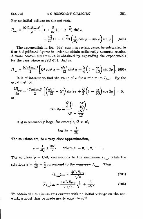
SEC. 95] A-C RESONANT CHARGING 391
For no initial voltage on the network,
(QCAU%4’I:m = ~
[
——l+~(l–e~)sinzp
——
( )1+4~(1–e~) &cosp–sinp sinp. (69a)
The exponential in Eq. (69a) must, in certain cases, be calculated to5 or 6 significant figures in order to obtain sufficiently accurate results.A more convenient formula is obtained by expanding the exponentialfor the case where nu/2Q <<1, that is,
Z;rm =
[ ( 4Q) 1““~)’ Q’ COS2q + ~ sin’ p + ~ 1 – ~ sin 2W . (69b)
It is of interest to find the value of p for a minimum I.,-. By theusual method,
– 2 [t$-Q2)sin2’+xaz:rm, = (CN-%d2ap
or
If Q is reasonably large, for example, Q >10,
The solutions are, to a very close approximation,
1~=43.+y, where m = 0,1, 2,....
The solution p = 1/4Q corresponds to the maximum I,,m, while the
1solutions p = — + ~ correspond to the minimum I,,-.
4Q 2Thus,
(l.rm)m= = Qcs (70a)
(1.-).. = “;C2 J + -&. (70b)
To obtain the minimum rms current with no initial voltage on the net-
1 work, p must thus be made nearly equal to ir/2.

392 THE CHARGING CIRCUIT OF THE LINE-TYPE PULSER [SEC. 9.5
Circuit Utilization Factor (C. U. F.) .—This factor is defined as
C.U.F. = — ( )‘m 1–3 ‘in’’’”
J ()
. (71)
4 Q2cos2p+~sin2q+~ l–~Q sin2@
For p = u/2, corresponding to the most common operating conditionfor a-c resonant charging,
Charging-circuit E~ency.-By definition, the efficiency q, is
(72)PN 1
‘c = p“ + I:~R, = ~ + Z&R.’
where
(C”EwJ’IzrmR. 2 [ Q’cos’’+%sin’’+ ;E)sin2nl&a&a— .
P. CN@&(n~)
2n7r
[ ‘(’ -9in2d4 Q*cos2W+~sin2q+z
.
()‘nff 1 – ~Q ‘in’ p
[ ()4 Qcot2p+n&+~ l–n< cotq4Q.
()
. (7:3)
‘“ 1–3
The maximum efficiency occurs when Z~_R./PN is a minimum.This minimum is obtained, to a very close approximation, when

SEC. 9.6] A-C NONRESONANT CHARGING 393
Thus for maximum efficiency p is very nearly equal to +7/2, in whichcase
4n%# nuI:=R, — ~Q12Q – ,— .
P.
()‘= 1–% 1–;;
and the maximum charging efficiency is given by
(74)
9.6. A-c Nonresonant Charging.-In resonant charging the voltagerise or gain may be considered a result of ordinary resonance multiplica-tion. In nonresonant charging, 1 – L,CNU~ # O, there is also a voltagegain which, if the duration of the transient is limited to one or two cycles,may even exceed that for resonant charging. The voltage gain for non-resonant charging may be considered a result of beats that occur betweenthe steady-state voltage of angular frequency O. and the transient voltageof angular frequency a. The voltage rises to high peak values for afew cycles, and then subsides to the steady-state values as the transientdies out. In resonant charging, on the other hand, the voltage rises tohigher and higher peak values, and the steady-state value is limited inmagnitude only by damping. It is clear, therefore, that damping can-not be important for nonresonant charging, except when resonance isapproached, that is, when u = u“. For transients with durations of oneor two cycles, however, damping may be neglected without makingserious errors, at least when calculating wave shapes,
Neglecting losses, the network charge as gi\-en by Eq. (54) may besimplified to
I=/QN=CNEb2l–a’
u
and
10 = limit tan-’ *“ = 0 ‘or%< 1’R.-o 1–+ l’r for ~ > 1.~. w

394 THE CHARGING CIRCUIT OF THE LINE-TYPE PULSER [SEC. 9.6
Full-cycle Churging.-The condition for repeating transients for full-cycle charging [see Eq. (58a)] gives, for n even,
(ie(0)— )~+~Qxsinqn7r u
cot—”—=2 w.
= tan $g~(0) – QN cos P
when R. = O (that is, a = O). Then
and Eq. (75) becomes
:(wa’-~) ““qN(t) = QN cOs (d + w – 8) + ii sin —
When t = O, the following expression may be obtained for A:
Equation (76) can now be rewritten
_ CNEb
[
Cos (Wat + w) + ‘%&-?)co5p_—
1–$n7r
sin~. —u. 2 1
The current equation obtained by differentiating Eq. (77) is
CNEti.i.(t) = —
1–$
(7; f
(78)

SEC. 9.6] A-C NONRESONANT CHARGING 395
The network voltage is derived from Eq. (77) and may be expressed inratio form vM/Eb, that is,
UP/(t) 1
[
—=— Cos(%t+ w)+ %(+?)C05VE,
1–$ sin ?.?% 2 1
‘N(”)sin:(oat-$). (,g)E~
sinfi.~WI 2
The voltage stepup ratio at the time (ad = rm)when the network dk-charges is
where p is related to i.(0), q.v(0), and u/oa by the relation
ab f ~az — 4ab2 + 1,sinp=—a2+l
in which
T1.Tu
(gN(0) +
a=:tan3GJb=
acrrEb .%)(l -3”
When i.(0) = O and q~(0) = O, the value of p reduces to
(80)
(81)
(82)
and the equation for voltage stepup ratio at the instant of discharge maybe written as a function of w/u~ alone, giving
The values of the stepup ratio and of p are plotted for one-cycle charg-ing (n = 2) as functions of coa/u in Fig. 9.17. The steady-state value ofthe network-voltage stepup ratio, neglecting losses, is also plotted here.When resonance is approached, that is, when w = COO,the steady-statevoltage ratio rises to high values. The transient-voltage gain is greaterthan the steady-state gain for certain values of O@/CO,illustrating thephenomenon of beats.

396 THE CHARGING C’IItCUIT OF THE LINE-TYPE PULSER [fkC. 9.6
The maximum stepup ratio for the transient case is about 3.66, andoccurs at us/u = 0.7 and p = 21°.
6
5 -
4 -
& 3~2 -
.s ~-s:0~W-1
! -2 -g
-3
/
-1s0E
-4 -
-5 ---270
-60 0,5 1.0 1.5 2,0
Us/id
FIG. 9. 17.—Voltage stepup ratio and phase angle as a function of ualu for a-c inductancecharging (circuit losses are neglected).
Curve A is the voltage stepup ratio for n = 2 (one cycle charging).Curve B is the voltage stepup ratio for n = m.Curve C is the phase angle .$.
Again it is of interest to obtain the average and effective values ofthe transformer currents. The d-c current may be obtained by integrat-ing Eq. (78) over the charging period Z’, = nT/u.. Thus,
where uat= z for convenience. Then
-(=)sin(x++f.Straightforward integration gives, for n even,
(84)
The rms current is calculated using the definition

SEC. 9.6] A-C NONRESONANT CHARGING 397
The evaluation of this integral is long and is not carried out here. Theresult, however, is
where
8$kcosqcos~;
+.
1
J (85)1–:
Half-cycle Charging. —Following the same procedure that was usedfor full-cycle charging, the condition for repeating transients when n isodd is
Substitution in Eq. (54) gives
An expression for A may be obtained when t = O,
+ A = qN(o) – Q. COS(q – t))—
nu co
coszr”zEquation (86) can now be rewritten
gN(f)= Q~ COS(f-d + w – f?)
[co,:; ]%(++qN(o) –Q.. COS((o – @
.2
C~E,
[
Cos 9= — Cos (Cd + $6) –( )]
Cos : Wat — u1–: mr u 2
Cos T g
‘~-(”’ --)
u mr
+ q~(o) ‘a “ 2 . (87’)mr u
Cos T E

398 THE CHARGING CIRCTJIT OF THE LINE-TYPE PULSER [SEC.9.6
The equation for current is obtained by differentiating Eq. (87). Thus,
i.(t) 1—. .CMEbWa
(
sin (uat+ q) –1–$ .O:(;:):sin[:c”t-%)l]
a
qN(o) @ ‘in:(”’’’-%)———cNEb U. m 0
CosT z
(88)
The network voltage is derived from Eq. (87) and may be expressed inratio form, that is,
Vz?(t) 1—. —Eb
[( )]
Cos (WJ + p) – co:: ~ cm; w! – ;1–$ Cos 7 F.
(89)
The voltage stepup ratio at the time (d = mr) when the network dis-charges is
vN(nr) 2 Cos p + UN(O)
x=–— “1–$2 ‘b
(90)
where p is related to i.(0), qN(()), and u/us by
For the special case where both the network voltage and charging currentare zero at time t = O, thk relation may be simplified to
–tan@=: tan;:.a
(92)
The direct component of current must, of necessity, be zero if n is oddby reason of symmetry. Therms current is obtained by integrating

SEC. 9.6] A-C NONRESONANT CHARGING 399
The result of evaluating this integral is
where
Figure 9.18 gives representative voltage and current wave shapesfor a-c nonresonant charging; (c) and (b) correspond to zero initial cur-rent and network voltage for half-cycle and full-cycle charging respec-
8
I4
IC—ocNEbtoa
-4
-8“Eo T 2X
8
4
I
o“
-4
-80 T m
8
4
0
-4
-8 Mo r 2r
(a) 0) (c)
(a) Full cycle, n =2; w./w =0.80; q =O”; UN(0) = –Ih.(b) Full cycle, n =2: @,7/o =0.70; p =21 °;u~(0) =0.(c) Half cycle, n = l;u~/w =0.50;@ =OO; UN(0) =0.
FIG. 9.18.—Voltage and current wave shapes for a-c nonresonant charging. Thebroken line is the impressed voltage.

400 THE CHARGING CIRCUZT OF THE I. TNE-TYPE PULSER [SEC.97
tively, and (a) is a special case of full-cycle charging. Figure 9. 18bcorresponds to the case of maximum voltage stepup ratio for full-cyclecharging.
9.7. Practical A-c Charging Transformers.-Jn all practical cases,the charging inductance used for a-c charging pulsers is built as leakageinductance into the transformer supplying the high voltage. A majorcomponent is therefore eliminated, with resultant savings in the weightand size of the pulser. The majority of a-c charging transformers fallwithin the following range of ratings:
Leakage inductance: 1 to 25 henrys.Secondary rms current: 0.05 to 1 amp.Secondary peak voltage: 5 to 30 kv.Kilovolt-amperes: 0.5 to 10 kva.A-c frequent y: 60 to 800 cycles/sec.
The leakage inductance of a transformer increases when the ratio of theMagnetic Magnetic
G
shunt shunt
IIA
“-~-~~-+11+” ~1111 ,,,1
F%nlarycoil
“JExciting core %cond~oil
Magnetic shunt \ Ar gap / Airgap
SectIon A-A Magnetic shunt
FIC. 9.19.—Sketch of an a-c resonant-charging transformer with a magnetioshunt; O. is the exciting flux and +, is thereactance flux. (CourteaU of GenaralElectric Co.)
primary flux cut by the secondaryto the total primary flux decreases.This decrease can be achieved inseveral ways:
1.
2.3.4.
By a physical separation ofthe primary and secondarywindings on the core.By the use of a magnetic shunt.By the use of a leakage core.By a combination of the abovemethods.
High-reactance transformers thathave a magnetic shunt or a leakagecore are commonly used because theleakage flux is more easily controlledby these means. Figure 9.19 shows a
typical magnetic-shunt transformer.‘l’he normal flux path through theexciting core of the transformer isindicated by FFF. The magneticshunts that provide a path for theleakage-reactance flux are locatedbetween the primary coil P and thesecondary coil S. These shunts are
composed of iron laminations of the same quality and thickness as thoseused in the main transformer core. By increasing or decreasing the

SEC.9.7] PRACTICAL A-C CHARGING TRANSFORMERS 401
spacing of the air gaps at the ends of the magnetic shunts, the leakagereactance of the transformer can be adjusted.
The magnetic-shunt transformer is simple in design and construction.There are certain current phase conditions on capacitive loads, however,under which the leakage-reactance flux and, the exciting flux add in sucha way as to increase the flux density in the two outside legs of the trans-former core. This increase may cause magnetic saturation of the ironin the core legs, with a correspondingincrease in core loss and decrease in Separate
agecor
inductance for the large values of sec-ondary current.
Figure 9.20 shows a transformer -4— A
having a separate leakage-reactancecore. The giesign comprises a primarycoil P and the secondary coil Swhich are linked by a normal excitingcore as shown. In addition, a leak- ‘3a~$~rak-age-reactance core containing an air Finishlayer
gap is provided in order to link the fi:ggsecondary winding and to serve asa magnetic path for the leakageflux. The spacing of this air gap con-
Airgap
trols the reactance and its physicalshape determines the reactance-versus-current characteristics of thetransformer. An air gap is also pro- SectionA-A
vialed in the exciting core in order to FIG. 9.20.—Sketch of an a-c re-
prevent its saturation by the direct-sonant-charging transformer with sepa-rate leakage core; & is the exciting flux
current component in the secondary and qh is the reactance flux. (Courteau
winding. OfGeneral Electric Co.)
The separate-leakage-core transformer has an advantage over themagnetic-shunt transformer because it provides a separate path for theleakage flux, and therefore prevents the leakage flux and the normalexciting flux from adding to produce saturation of the steel. A trans-former of this type requires two separate cores, but is comparable tothe magnetic-shunt transformer in simplicity of design and construction.A transformer having a separate leakage core requires approximately10 per cent more space than that having a magnetic shunt, but theadditional space has not limited its applications. Figure 9.21 shows theassembly of cores and coils for a transformer with a separate leakage core.The various parts can be recognized by comparison with Fig. 9.20.
Linearity Requirerrwnts for A-c Charging Transformers.-The switchesused in a-c charging pulsers are nearly always rotary spark gaps, which

402 THE CHARGING CIRCUIT OF THE LINE-TYPE PULSER [SEC. 9.7
have complex operating characteristics. Perhaps the most importantcomplicating factor encountered with rotary-gap pulsers is the increasein spark length with power level. This increase in gap length changesthe a-c voltage phase at which the spark occurs, thereby disturbing thecharging-circuit conditions. The phase of the a-c voltage may also bechanged by the effect of the load current on the alternator magnetic field.
——.-—_ .FIG.9.21.—Core-and-coilassemblyof
a high-reactancetransformer. (CourtesyOJGeneral Electra2 Co. )
As a result, transformers havingconstant leakage inductance for allcurrents in the operating rangeusually do not give the best over-all performance. Since an exactanal ysis is difficult, the final adjust-ment of the inductance characteristicof the charging transformer is alwaysmade by experimental observationon an electrical sample of the pulsercircuit, including the alternator.
The leakage inductances of charg-ing transformers are measured bythe same methods as those used ford-c charging remtors (Sec. 9.2). Thetransformer primary is short-cir-cuited and superimposed a-c and d-ccurrents are passed through the sec-
ondary. In the case of half-cycle a-c charging, the direct cur~ent in thetransformer is zero. When testing full-cycle resonant charging trans-formers, the a-c to d-c current ratio is taken as 2.9, but for nonresonantcharging the ratio is larger. The value of 2.9 is derived as follows. Forfull-cycle charging (n = 2) Eq. (70b) reduces to
(I-).n = “*The corresponding average current from Eq. (67a) is
()I.a, = ‘cNEwa 1 – e?2T 1l+=
Hence,
(94)
(95)

SEC. 9.7] PRACTICAL A-C CHARGING TRAN,$’FORMBRS
The a-c component of the secondary current is given by
Hence the a-e to d-c current ratio is
I C.-c _
-G
47r2 _ ~I– 2.c.”
61–2
403
(96)
Using representative value for the quality factor, that is, Q = 10,the a-c to d-c current ratio is found to be 2.9. For zero circuit loss, thatis, Q = ~, the ratio is reduced to 2.37.
The charging-current wave for the case of a-c resonant charging withzero initial voltage on the condenser and zero current is shown in Fig.9. 16b, where the form of the a-c component of the current is seen to beapproximately sinusoidal. The maximum value for this a-c componentis 1.62C.vEz@a, whereas the peak value of the corresponding sine wave,calculated for Q = 10, is 1.84cNEwa. Since the inductance-measuringmethod closely simulates the current under operating conditions thevalues of leakage-inductance determined by this method may be con-sidered to be significant.
The inductance of the charging circuit includes that of the a-c alter-nator or other a-c voltage source. The effective inductance of the specialalternators used with a-c charging pulsers may be from 10 to 20 per centof the total inductance, and must be subtracted from the calculated valuein order to obtain the net leakage inductance required in the chargingtransformer. The effective alternator inductance is difficult to calculatein any given case and is also difficult to measure, except when it is useddirectly in a pulser circuit.
A transformer to be used with an a-c charging rotary-gap pulserusually gives the best over-all performance if its leakage inductancedecreases slightly with increasing current. The leakage-inductancecharacteristics for two representative transformers are shown in Fig.9.22, that in Fig. 9“22a having a magnetic shunt, and that in Fig. 9.22b aleakage-rezctance core. As is to be expected, the transformer using aleakage-reactance core has the more linear characteristic. The allowableamount of decrease in the inductance characteristic is estimated byexperience, and the final adjustment is always made on an actual testpulser.
B-H Oscillograms for Typical A-c Char~”ng Transformers.-Theleakage-inductance characteristics may be shown by graphs such as those

404 THE CHARGING CIRCUIT OF THE LINE-TYPE PULSER [SEC. 9.7
in Fig. 9.22. The B-H oscillograms, however, are more fundamental,and reveal in detail the effects of transformer-core saturation. Twocomplete sets of B-H oscillograms for the same transformers as those ofFig. 9.22 are shown in Fig. 9.23 and Fig. 9.24.
%REEli0 50 100 150200 250 300 350 0 0.20.40.6 0.8 1.0 1.2
Iew in ma Ie ~= in amp
(a) (b)(u) With a magnetic shunt;rated1.- = zoo III*.(b) With a separate leakage core; rated IC~e = 1.2 amp.
)?m. 9.22.—Leakage inductance vs. secondary a-c current for typical a-c chargjngtransformers.
An ideal a-c charging transformer is one that has zero internal 10W,aa well as a constant stepup ratio and leakage inductance over the rangeof voltage and currents used. The B-H oscillograms for such a trans-former would consist of straight lines enclosing zero areas, instead of theloops enclosing fbite areas that are actually observed. The leakage-inductance B-H oscillograms for well-designed charging transformersalways enclose small areas, indicating that the losses are relatively small.The linearity of the B-H loops depends to a great extent upon the typeof leakage-flux path used in the transformer. Transformers withmagnetic shunts usually show the greatest saturation effects.
The oscillograms in Fig. 9.23 are good examples of this tendency sincethere is a slight amount of saturation even at one-third rated load cur-rent when direct current is present. The curvature of the remainingB-H loops increases, although not markedly, with increasing current.As indicated by theory, the removal of the direct-current componentlessens the degree of saturation. The other oscillograms in the samefigure show the secondary exciting current when the primary is open-circuited. Since the areas of these loops are considerably greater thanthose for the leakage inductance, it is evident that the core losses aregreater. The high degree of saturation induced by both the over-voltageand the direct current is indicated by comparison with normal B-H loopsfor the transformer-exciting current.
The set of B-H oscillograms shown in Fig. 9.24 are for a transformerwith a separate leakage core, and form an interesting comparison. Theleakage-flux oscillograms indicate very slight saturation of the leakage-

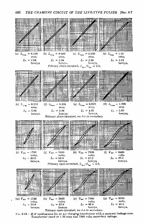
406 THE CHARGING CIRCUIT OF THE LINE-TYPE PULSER [SEC.97
(a) Icr,,u = 0.’230 (b) 1.,,,,, = 0.4(;0 (c) 1.,”1, = 0,690 (d) I.rJu, = 1,06Ulllp, Mllp, ‘iMllp, amp,
LL = 2.94 LL = 2.94 L. = 2.94 LL = 2.83hcmys. hen,>-.. henrys. henrys.
Primary short.circuited, I,q-JI,,v = 2.9.
(e) 1,,,,,, = 0.215 (~) Ic,r,u = 0.4:35 (0) I.,u = 0.870 (h) I.r,rm = 1.000amp, amp, amp, amp
L, = 2.94 ],’ = 2,98 LL = 2,92 L. = 2.89
henrys. hcm’ys. henrys. henrys.Primary short-circuited, no {1-c in secondary
(i) V,,w = 1700 (j) v=. = 3460 (k) v... = 7500 (1) Vs.. = 8600volts, volts, volts, volts
I,’ = 52.0 L. = 54.0 LL = 47.0henrys.
L. = 49.5henrys. henrys. henrys.
Primary open-circuited, I,e-e /I,,V = 2.9.
(m) V.= = 1730 (n) VU. = 3460 (o) V,m = 7500 (p) v= = 8600volts, volts, volts, volts,
I>. = 54.0 L. = 52.0 L. = 48.4 LL = 46.6
henrys. henrys. henrys. henrys.Primary open-circuited, no d-c in secondary.
FWS.9.24,—B-H oscillograms for an a-c charging transformer with a separate leakage core.Transformer rated at 1,20 amp and 7500 volts secondary voltage.

SEC. 9.8] DESIGN OF HIGH-REACTANCE TRANSFORMERS 407
flux core. Likewise, the direct-current component has only a very smalleffect on the measured values of the leakage inductance. The oscillo-grams for the secondary exciting current are also of a somewhat differentcharacter than those for a transformer of the magnetic-shunt type. Thedirect-current component has less effect on the degree of core saturationin the latter case. Unfortunately, however, limitations in the measuringapparatus prevented the overvolting of the secondary, and it was there-fore impossible to obtain a complete set of comparative data for the lattertransformer.
9.8. The Design of High-reactance Transformers. ~Only the designproblems specifically related to high-reactance transformers are discussedhere since those common to both d-c charging reactors and a-c chargingtransformers are treated in Sec. 9.3.
The determination of the effective voltage stepup ratio and the induct-ance of the transformer is made by calculation and by experiment.Theoretically, the total reactance in an a-c resonant-charging circuit ofthe full-wave type should be about 194 per cent, that is,
wucm,47.= 1.94.
The series reactance of the power supply and the high-reactance trans-former are combined to give this reactance. Nonlinearity of the trans-former inductance may be provided by extending the length of a few ofthe laminations on the leakage core, thus providing a short gap of smallcross section in parallel with the main gap.
Pulse-formingVN nehvork
[
supply supply
FIG. 925.- --Diagram of a line-type pulser using a-c charging.
F@re 9.25 shows the general circuit in which a-c resonant-chargingtransformers are used. The pulse transformer shown does not contributein any way to the characteristics of the charging circuit; hence, for most
‘By H. H. Koski of the General Electric Company, Pittsfield, Mass,

408 THE CHARGING CIRCUIT OF THE LINE-TYPE PULSER [SEC. 9.8
purposes, the impedance of the pulse transformer can be considered tobc zero, except during pulsing.
Figure 9.26 shows the equivalent circuit of the diagram given inFig. 9.25. The induced voltage, usually sinusoidal, in the generatorarmature is shown by Vc. This voltage is applied to the resistance andreactance components of the a-c generator, resonant-charging trans-former, and the capacitance CN in the pulser circuit.
R. XCy
I1
Resonant<hargmgtransformer
1,’IG. 9.26.—Equivalent circuit of a line-type pulser using a-c charging.
Typical oscillograms of the voltage output of the transformer in afull-wave charging circuit are shown in Fig. 9.27. The exponential decayin the voltage after the pulse is caused by the time constant of the viewingcircuit that is used in conjunction with a cathode-ray oscilloscope toobserve the charging waveform.
fb) Fast sweem(a) Slow sweep.F[c, 9.27.—Cl~arging voltage wave shapes in an a-c ‘charging line~type pul.xx. (CourtesU
of Gencnd Electric Co. )
Sample Design.—The following sample calculations show the generalprocedure follo~red in the design of a transformer having the followingspecifications:
Input: 115-volt, 635-cycle.Effective turns ratio: 1/49.Inductance: 6.2 henrys + 5 per cent.Current in high-voltage winding: 0.330 amp rms, 0.114 amp d-c,Recurrence frequency: 635 pps.Peak charging voltage: 21.8 kv.

SEC. 9.8] DESIGN OF HIGH-REACTANCE TRANSFORMERS 409
Full-cycle charging circuit.Efficiency: 90 per cent.Ambient temperature range: – 40°C to + 50°C.For shipboard use.Hermetically-sealed unit, dimensions not specified, mounting to be
by means of a clamp over the top edge of the tank.PFN capacitance: 0.0091 pf.Generator impedance: 3.9 ohms.
For this case, tests indicated that an actual turns ratio of 1/44 wasrequired instead of the theoretical value 1/49; in the same way, the neces-sary transformer inductance was found to be 6.2 henrys as against 5henrys indicated by the original computations.
This transformer was designed to have a separate leakage core (Fig.9.20), but the calculations can, in general, be applied to one having amagnetic shunt. Figure 9.21 shows the core and coil of the assembledunit. The design calculation is started by choosing values of maximumflux densities compatible with previous experience. Selecting 27,000and 40,000 lines/in. 2 for the flux in the main and leakage cores respec-tively, and a cross section of 3 in. by ~ in. for the main core, the voltageper turn may be found by the formula
“ =%’x ‘cxA’x10-8’where A, is the net area of steel or the cross section multiplied by thespace factor. Assuming a value of 0.88 for this factor gives
V, = 4.44 X 635 X 27,000 X 3 X f X 10–s volts= 1.76 volts.
Hence, the coils require 65 and 2860 turns respectively.The leakage-reactance core can now be determined. Its flux is
given by
~lk =L. x I.m= x 10’
N’
where Ic= = 1.81 C-, and N = number of high-voltage turns. Then
@Vk=6.2 X 0.33 X 1.8 X 108
2860= 129,000 lines.
Past experience indicates that about 20 per cent of this flux is externalto the leakage core, leaving only 103,000 lines in the core. The cross

410 THE CHARGING CIRCUIT OF THE LINE-TYPE PULSER [SEC.9.8
section of the leakage core at 40,000 lines/in. z equals
103,000— = 2.58 in. z40,000
This value closely approximates that for the main-core cross section.For mechanical reasons, the same section is used for both cores, giving aflux density
~ = 103,000c
2.36= 44,600 lines/in.2
in the leakage core. This value is approximate and must be corrected
later w-hen the ftux external to the core is calculated.
The coils can no~v be designed. In order to stay within the allowable
current density at full load (assumed to be 1300 amp/in. 2,, the secondary
conductor must be 0.0179 in. in diameter, and the primary 0.120 in.
by 0.090 in. The latter cross section corresponds to the equivalent value
of the a-c component of the high-voltage current plus the core-exciting
current. The conductor shape is determined solely by the complete
coil-shape desired and the wire sizes on hand.
‘l’he lo~v-voltage \vire is chosen with paper insulation, making the
ov~r-all insulated size O.131 in. by 0.101 in. TTVO layers are necessary
for the coil and a sheet of 0.015-in. insulation between the layers serves
as mechanical support for the second layer.
In order to reduce the voltage induced in the primary by the discharge
of the pulse-forming network and thus to minimize radio-noise inter-
ference, a grounded electrostatic shield is interposed between the \vind-
ings. This shield consists of a brass screen insulated from the coil by a
sheet of 0.015-in. layer insulation forming one open turn around the
coil. It is bonded to the core clamp and hence to ground. Some insula-
tion must be between the ends of the shield to prevent a short-circuit.
The high-voltage m-ire is constructed with double enamel and cotton
covering, which makes its nominal over-all diameter equal to 0.0246 in.
In order to distribute the voltage stresses more evenly under the impulse
conditions of operation, the last layer is made of more heavily insulated
~vire, as shown in Figs, ~. 19 and 9.20, This w-ire insulation consists of
~-in. black varnished cambric insulation, w-hich needs only a few turns
for a full layer; thus, the number of turns of the 0.0179-in. wire is reduced
accordingly.
The insulation in the transformer consists of the coil cylinders, paper-
layer insulation in the coils, pressboard collars and barriers, wooden
spacers, and oil,Because of the mechanical strength required, the coil cylinders present
no problem in electrical insulation. The layer insulation in the coils,

SEC.9.8] DESIGN OF HIGH-REACTANCE TRANSFORMERS 411
thecreepage distance around the ends of the layers, the collars and bar-riere between the high-voltage coil and the cores, and the insulation ofleads are all determined from the corresponding applied voltages and thelimiting values of stress. Some of these values are calculated directly,but others must be obtained from a scale layout of the transformer.Another reason for using a scale layout is the necessity of measuring thecross-sectional areas of the coils and the area between coils in order tocalculate the air and iron fluxes more accurately.
Lecdcage-reuctance-core Gap.—The preliminary calculation of the fluxin the leakage-reactance core was based on an estimate of the flux inthe air external to the core. The air flux is now calculated from theactual dimensions of the transformer in order to give a more accuratevalue of core flux for use in determining the gap in the leakage-reactancecore.
The flux I#Jlexternal to the core isl
whereAh = cross-sectional area of the high-voltage coil in in. 2,A i = craw-sectional area of the low-voltage coil in in.z,
A ~h–lj = area between the coils in in. 2,h = length of winding on the high-voltage coil in in.,
and
( )3.19 ~ + 5.85 + ~ (2860)(0.330)(1.8)+, =
(0.65)(4.25)= 23,200 lines.
Siice a total flux of 129,000 lines was previously calculated, 105,800 linesare left in the core.
Because of the effect of “fringing,” the calculation of the core gapis a trial-and-error process. The actual length of the gap is used, but itscross-sectional area is increased by an empirical amount that is a functionof the length.
First, the ratio of effective area to length of the leakage-reactance coreis calculated;
A,
~ = (3. 19~:NZ~)
where A ~ = effective gap area, 1~ = gap length, and I$Z= core flux.
1The factor 0.65 in the denominatoris empiricaland dependson the coil configu-ration. Ita value may vary from 0.6 to 1.1.

412 THE CHARGING CIRCUIT OF THE LINE-TYPE PULSER [SEC.98
There results
A 105,800——l*Q – (3.19)(2860)(0.330)(1.8) = 19”5 ‘n”
Assuming a gap length of 0.160 in., the effective area is calculated from
where A. is the actual cross-sectional area of the gap, and pg is theperiphery of the gap.Therefore
A,= 3 x ~ + ‘0”160~(7”75)
= 3.03 in. zChecking,—.
~ _ 303A
1, 0.160 = 19”0 ‘n”
A gap length of 0.155 in. would almost exactly check the value calcu-lated for A./1, but the value 19.0 is within the design limits.
A gap of this length is satisfactory, but a nonlinear inductance givesmore stable operation. The ordinary gap gives an almost linear induct-ance. By experiment, a nonlinear inductance is obtained by makingthe gap with several of the outside laminations extending into the gap.At low currents the short gap between the extended laminations gives ahigh inductance, but at high currents these extended laminations becomesaturated, causing the effective length of the gap to increase. Theinductance at high current is therefore decreased by some value depend-ing on the proportions of the gap. The final design has about a 15 percent drop in inductance from ~ to full current. This gap constructionrequires preliminary tests on the cores in order to adjust the spacing tothe right value.
Losses.—The losses in the transformer are important not only fromthe standpoint of resonant-voltage rise but also from the point of view ofefficiency and heating. The losses, shown in Table 93, consist of Z2R-
and eddy-current losses in the windings, core loss, and stray loss, which isan all-inclusive term covering indeterminate losses in the insulation, theclamps, and the tank.
The ratio of the expected voltage rise to the applied a-c voltage in aresonant-charging circuit is given by the relation (66b) which, in thiscase, reduces to
V. nu
()z l–~”,—.—
Eb 4Q

SEC. 9.8] DESIGN OF HIGH-REACTANCE TRANSFORMERS 413
where
Hence, for full-cycle charging.
~ ~ 2.98E~ “
The leakage-core loss is calculated by assuming that the wave i$ ~unsymmetrical, that is, the first peali has only half the voltage of thdsecond peak. The stray loss depends greatly on the mechanical propor~- .:tions of the transformer and can be estimated only from experience; ineatransformer of this type it is usually about equal to the total coppe~o$..- ~
t)TABLE93.-TRANSFOIWERLOSSES .,
watts full l&‘j
a-c iesOnant-LQss
char’~:;?p” :In primary coil 12Rplus eddy-currentloss . . ., ., . . . .
{
121ZP]uscddy. 17.71:-’””:In secondarycoil Leakage-corcloss. . . . . . . . . . . . . 29.0 :. j
Stray loss. ,,, . . . . . . . . . . . . . . . . . . ~[:.~~ti.j :P.
Total loss incharging circuit, P.. . 90.16~@In exciting core . . . . . . . . . . . . . . . . . . . 24,4
Total transformer loss....,,.,.,,.. 114.56
Heating and Oil E~pansion.—The operating temperature of the wind-ings, core, and oil is determined by computing empirically the tem-perature drop from the wire and core to the tank surface through theinsulation, the oil, and the contact surfaces. In this particular example,the losses correspond to approximately 0.2 watts/in. 2 of tank, giving atemperature rise of 25°C from ambient air to oil. The temperature risein the oil from tank to coil depends on conduction and convection, andmay amount to 15°C in this transformer; the rise from the coil to thewindings amounts to about 10”C for a coil construction of the particulartype used in this case. The temperature rise of the core above oil,resulting from a dissipation of about 0.25 watts in.2, is also about 10°.The temperature rise of both coils and core above the external ambienttemperature is therefore about 500C.
In this” particular transformer, an air space is provided in order tolimit changes in pressure inside the tank, resulting from temperaturevariations that cause the oil to expand or contract. The expected pres-

-114 THE CHARGING CIRCUIT OF THE LINE-TYPE PULSER [SEC.9.9
sure is then calculated from the following empirical formula:
~ = 1470V,5T + 65.4T29,800V. + 0.0147T2’
whereP = absolute pressure in lb/in.2,T = final gas and oil temperature absolute in “C,
Vz, = ratio of air volume to oil volume at 25”C,V, = ratio of air volume to oil volume at T“C.
If a final oil temperature of 80”C is assumed, VX, = 0.0715 and VT
= 0.0276, giving a pressure of 22.7 lb/in.2 if there is no flexing in the tank.In practice, the elasticity of the sides of the tank reduces that pressureappreciably.
9.9. Miscellaneous Charging Circuits. A-c Dwde Charging.—A sim-ple method for a-c charging, mentioned in Sec. 9.4, is to insert a hold-off
Hold.ofl dtiediode between the high-voltage transformerand the network as shown in Fig. 9.28. As
3 ~“-fNeiviuirillustrated by Fig. 9.29, the voltage on the net-
Eb sin’wat ~~ ~:..? work builds up to almost the peak positive
Tmnshmnervalue of the transformer voltage. The hold-
Fto. 9.28,—Schematiccir- off diode prevents the reverse flow of current,cuit diagramfor a-c charging and therefore maintains the charge on the net-using a hold-off diode. work until the switch is fired. The dischargeof the network is timed to take place during the negative half cycle ofthe transformer voltage in order to insure a long deionization time fortlie switch.
The equations for a-c diode charging are developed on the assump-ti,ms (1) that the transformer has zero leakage inductance and (2) that
tCharging Hold-ofr Oischarge
period periodal Y
‘ /[
point
M \ ‘\\
g \ \\
s \ \
\ \ \
\ I I
o0 q /2T \ 31r I’m
\\ ;)~, i -“;
‘x-I’ Transformer%~’voltage \
FIG.9.29.—Voltagerelationsfor a-c diodecharging.
the diode loss’ can be represented by an equivalent resistance. Thedifferential equation and initial conditions for the network charge g~during the charging period are

SEC.9.9] MISCELLANEOUS CHARGING CIRCUITS
q..(o) = o,
(-)
dq~
dt ,=0= o.
The correspondhg Laplace-transform equation is
EbuaRcPqdP) + +Nqdp) = p, + ~:”
Solving for q~(p),
415
(98)
The inverse transform giving q~(t) is
By differentiating, the current may be found to be
The maximum voltage on the condenser occurs either for i.(t) = O,
or for a value of t = tlgiven by setting Eq. (100) equal to zero. Thent,is a solution of
oaf,RCC,.W.sin cot, + cos a.tl – e- ‘Cc””” = O. (101)
By substituting Eq. (100) into Eq. (99), the relatio~
(qN)mx = cNEb SkI (d]
is obtained. For most practical cases of a-c diode charging, RcCNua <<1.
For example, if R.CWOa = 0.04, the exponential term in Eq. (101) isnegligible, and w.tiis given approximately by
–1tan uatl= —
R.CW.or Coatl= ; + R. CW.O..
Using this value of d,, (~N)msxbecomes
(102)
to a very close approximation. When R.CNwa is not small comparedwith unity, the more exact equations must be used. For the remainingcalculations, it is assumed that R, C,WO. <<1, and the average and effec-

416 THE CHARGING
tive currents are found
and
respectively.
CIRCUIT OF 7’HE LINE-TYPE PULSER [SEC. 9.9
to be~ = CNEWa
‘*V 21r
(103)
The transformer utilization factor, T. U. F., or ratio of power output totransformer volt-amperes, is then
u.% “ ; CNE; 1 = 0,32
T.U.F. =Eb C~Ewa = ; ‘—.—
@i 24
and the charging efficiency, q,, is given by
%_ power output = % “ ; ‘NE; 1
“ – power input C~E&o~ ~ =, (104)
~C.E:+7 . 1 + ~ RcCNtia2“2
if the core loss in the transformer is neglected. Both the diode resistanceand the transformer effective resistance must be included in R..
A-c diode charging normally has a high efficiency if a suitable diode isused. The method has the advantage of being simple and requiring noadjustments. On the other hand, it has the disadvantage of having avery low T.U. F. and requiring a high-voltage diode. These disadvan-tages limit its use to.relatively low-power circuits.
A variation of the a-c diode-charging circuit is one in which a resonat-ing inductance is includep. in order to increase the network voltage.Neglecting losses, the maximum voltage on the condenser is increased
g}
by a factor of 7r/2 and the T.U.F. is like-wise increased. This circuit has no advan-
3 ‘Hold.off - ~ewwk tage over the a-c resonant-charging circuit,dwdes ,:~#& however, except in the case where the a-c and
Tm.nsformerJ the recurrence frequencies are subject to con-
siderable variation.F1~,930.-Two-diode chwg- The a-c diode-charging method may be ex-
ing circuit. tended to full-wave charging by using twodiodes in a manner similar to the ordinary voltage-doubler rectifier cir-cuit. The two-diode charging circuit is shown in Fig. 9.30.

CHAPTER 10
PERFORMANCE OF LINE-TYPE PULSERS
BY J. V. LEBACQZ
In the preceding chapters the behavior and performance of t(Ievarious components of the pulser and of the discharging and chargingcircuits are considered separately. In most of the discussions it is alsoassumed that the pulser load stays constant, both from pulse to pulseand during one pulse. In practice, however, the load is not always thesame from pulse to pulse, and there are special conditions that requi~e aconsideration of the entire pulser circuit. Faults can occur in some ofthe components or in the load, and it is necessary to devise protectivemeasures in order to limit the resulting damage to the other components.Some magnetrons exhibit spurious characteristics, such as mode-changingor sparking, which can be alleviated by careful pulser design,
The purpose of this chapter is to indicate some of the principles to befollowed in the design of the pulser as a whole in order to obtain the mostsatisfactory operation that is compatible with the load cliaracteristics.
10.1. Effects of Changes in Load Impedance.—The purpose of thissection is to discuss the effect on the pulser circuit of sudd(,n variations inload impedance, either from pulse to pulse, or during one pulse. Smallvariations in load impedance usually have little effect on the operation ofthe circuit. This fact can easily be understood by the l;onsiderations ofpower transfer, discussed in Sec. 7.2, which show tha L little change inoutput power is introduced by a slight mismatch betwven the impedancesof the load and the pulse-forming network. This statement, however,must be qualified when the entire pulser circuit, including the chargingcircuit, is considered. It can then be shown that the effect may not benegligible if a unidirectional switch is used.
Of more direct concern are the effects of large variations in loadimpedance which are usually produced by faulty operation of the load,such as an open circuit or a short circuit. Either one of these conditionsmay occur for an indefinite length of time, for only one or a few pulses insuccession, or—as, for instance, with some sparking magnetrons-theymay be expected to repeat at irregular but frequent intervals. Thegeneral measures taken to protect the circuit agail ,st such load behaviorare considered in this section, and a more completfi :Ir)ulysis of the opera-tion of the pulser with a sparking magnetron is give t ‘f~i${ec. 10.3.
417

418 PERFORMANCE OF LINE-TYPE PULSERS [SEC.101
E$ect of Load on Pulser Operation. -In Sec. 7“1 it is shown that thecurrent and voltage supplied by an ideal pulser discharging a pulse-form-ing network of impedance ZN into a resistance Rl are given by
andR, VN
Vi=— .R1 + Z.
The voltage left on the network at the end of the pulse is given by
‘1– ‘NVN.VN-1 = El + ZN
(1)
(2)
(3)
If R1 > Z., VN-1 has the same polarity as Viv, and the voltage left onthe network discharges through the load, giving reflected pulses ofamplitude
‘zn=EI:zN~*NbN>
where Vz. is the voltage of the nth reflected pulse following the principalpulse. Obviously, if the load is a biased diode, the reflected pulses inthe load appear only as long as the voltage left on the network VN_. isgreater than the bias voltage Vs, and the value of Rl changes with eachsuccessive step. If V, > VN_., the discharge takes place entirely throughshunt paths in the pulse transformer.
If Rl < Z,v, three cases must be considered. If the load is a resistanceand the switch is perfectly bidirectional, voltage left on the network dis-charges through the load in the same fashion as when Rl > Ziv, andreflected pulse voltages appear across the load, the successive voltagesbeing of opposite polarity. If the switch is unidirectional the voltagegiven in Eq. (3) is left on the network, since its discharge requires a cur-rent of polarity opposite to that of the main pulse flowing through theswitch. This voltage affects the amplitude of the network voltage atthe end of the following charging cycle in the manner described below.
If the switch is imperfectly bidirectional—that is, normally passescurrent in either direction but may hold off some voltage of either polaritybecause deionization sets in—this voltage affects the following chargingcycles and, since it is random in nature, may also cause random varia-tions in the peak network voltage.
The following discussion applies to the relatively simple but veryimportant case of a pulser using d-c resonant charging and a unidirectionalswitch. A constant load resistance R, is assumed, instead of a biased

SEC.10.1] EFFECTS OF CHANGES IN LOAD IMPEDANCE 419
diode load. The voltage at the end of the nth charging period is given by
R.T,——v.. = EW + (Ew – v~..,)e ‘Lo n=l,2.
where V,m = V~n_, is the voltage left on the network byas derived from Eq. (3) and shownin Fig. 10.1. VNand
tT,=j=~T,
r ~hm
~.2Thus z>
. , (917a)
the mismatch
VN.4
r I 1 1 1——vNm = EW + (EM – V’,..,)e 2Q, T VN.~
U Time -
where fi. ,Q=~=~~”
c c (a)
This equation can be rewrittenv
.——
w
v ‘N3 “VN. = EM(1 + e ZQ) – VJn_,e–~ ! v ‘z
N&r—— s
or, letting ~ = e ZQand considering ~the charging cycle following the first Tr Time-pulse, VJ1 v= VN.,
VN, = EM(1 + ~) – TV,,. (4) J2= VN2., ~, = VN4.1,3 = VN3.1
If the value of VJ, = V~_, is intro-V
duced from Eq. (3), and (b)
R, – ZNFIO. 10. 1..—Network voltages if the
load resistance is smaller than the net-‘ = m.’ work impedance. (a) Bidirectional
VJ, = KV,V= K&,(l + ~). switch; successive reflections. (b) Effect
Thusof inverse voltage on successive chargingcycles with a unidirectional switch and
VN, = I%(I + 7)(1 – TK).d-c resonant charging.
At the end of the second pulse, the voltage left on the network is given by
V,, = KVN,,
and at the end of the third charging cycle the network reaches the voltage
V., = EM(I + T) – 7KVN, = EM(1 + T)(I – ~K + ~’K2).
Similarly,V,, = KVN8
andV., = EM(1 + -Y)(1 – ~K + ~2K2 – @K3). (5)

420 PERFORMANCE OF LINE-TYPE PULSERS [SEC. 101
when it is assumed that R1 < Z,V, K is always negative, and Eq. (5) canbe renritten
VN, = J%(I + T)(1 + 71x]+ 7’]K12+ 731K13).
After the nth pulse, the network recharges to a voltage
VW.+,) = J%(1 + 7)(1 + 71K]+ 72)K]2+ “ “ “ + 7“IK]”),
which can be rewritten
1 + T 1 – ~n+llKln+l).VN[,,+,,= EM ~ (
When n approaches infinity, the equilibrium network voltage is given by
(6)
This equation brings out the fact that, for unidirectional s~~itches, thenetwork voltage can easily be more than twice the supply voltage. If,for instance, it is assumed that 7 = 0.91 and K = – 0.1, correspondingto a normal charging circuit and a 20 per cent mismatch between the loadand the network (which is perfectly admissible from power-transferconsiderations),
Such charging stepup ratios are common in line-type pulsers usingunidirectional switches when no measures are taken to discharge theinverse voltage left on the network. In general, it is not necessary toprovide a discharging path except when misbehavior of the load isexpected.
The effect of a mismatch such that RI < 2., on the over-all operationof the pulser using a unidirectional switch may be considered briefly l)ydetermining the voltage and current input to the pulser circuit requiredfor a given pulw output.
If a unidirectional switch is used, the peak forward network voltageis given by Eq. (6).Since
Eq. (6) can be rewritten2 l+K~
Ebb= vl— —l+~l+K”
The power-supply current, given by Eq. (919), is
(7)

Fttr.10.1] EFFECTS OF CHA NGIM IN LOAD IMPEDANCE
and the avernge power supplied to the pulser is
4~: (1 + 7K)(1 – K)pi = EMIt,V = j,c. ~y
(1 + K)’ “
421
(8)
For n pulaer using a Iidirectiomd switch to supply the same power to thesilme load
v. = EL(1 + -y)or
2vl
‘~ = (1 + 7)(1 + .x)
I:-y = f,CNVN = frcN +KI
and4V;
H = frcN (1 + 7)(1 + K)’” (9)
The ratio of Eqs (8) and (9), which is the ratio of the power inputs tothe pulser required to obtain the same output into the same load, is
p = (1 + ~K)(l— K). (lo)
Since the unidirectional switch conserves energy on the network aftereach pulse, the ratio P might be expected to be always less than unity.As can be seen by examination of Eq. (10), however, p can be greaterthan one because of the decrease in charging efficiency when inversevoltage is present on the network. If y = 1 (100 per cent charging .efficiency),
P=l– K2 <1.
For any other value of 7 between O and 1, the expression (10) can berewritten
p=l—~K2—K(l—T).
Since K is ahvays negative for Rl < Z., the second term is negatiye, butthe third term of the expression is positive. Accordingly, p is smallerthan unity only when
~K2 > K(1 – ~),
or
The considerations outlined above are based on the assumption of anideally simplified circuit consisting of a network, a switch, and a resistance

422 PERFORMANCE OF LINE-TYPE PULSERS [SEC. 10.1
load. If a biased-diode load is considered, the analytical expressionsbecome more complicated because of the change in operating point withchange in network-barging voltage, which C@USWthe coefficient K ~
decrease slightly after each pulse. Some equilibrium network voltage iseventually reached, however, because the quality factor of the charging
m
FfNreactor is not independent of the applied volt-age, resulting in a decrease in ~ with ankcr~ b (VN – EM).
Le If a pulse transformer and a bhsed-diodeload are considered, network inverse voltage.appears even though the operating point of theload matches the network impedance, as can
Fm. 10.2.—Equivalent be seen by considering Fig. 10”2 in which all dia-diaoharcins circuit used to turbing elements except the shunt inductancentudyinversenetworkvoltage. of the pulse transformer have been neglected.
At the end of the rectangular pulse of amplitude VI and duration r)
the current flowing in this inductance can be expreaaed by i~ = ~a T,
and the energy stored in it by
At the end of the pulse, this energy charges the storage condenser of thepulse-forming network to a voltage V, such that
For matched conditions,
.
and’
(-)v, 2 1 +- —.
VN = 4 L.(7N
However,.r . 2G7NZN = 2 ~L~,
and hence, to a firat approximation,
v, IILN—.—VN z.’
(11)

SEC, 10.2] SHORT CIRCUITS IN THE LOAD 423
where the sign is determined by the direction of current flow. Assuming7 = 2.5 ~SW, Z~ = 1200 ohms, and L. = 45 mh,
L. = ‘~’ = 1.5 X 10⁻³ henrys,
and
The values obtained from Eq. (11) are usually greater than thoseobtained experimentally because losses in the circuit and in the dis-tributed capacitances normally absorb or dissipate part of the energy thathas been assumed to be returned to the network capacitance. Thesevalues are sufficiently accurate, however, for use in the preliminary designof a pulser.
1002. Short Circuits in the Load.—Two cases must be consideredwhen studying the operation of a pulser when the load is short-circuited:
1. That for a unidirectional switch.2. That for a bidirectional switch.
The fundamental concepts of operation discussed earlier in Sec. 10.1are now amplified.
Circuit Using a Unidirectional Switch. -It has been shown that theequilibrium output voltage is given by Eq. (7), that is,
Rl – z.where ~ = e‘% is de~rmined by & charging circuit,, and K = —
R1 + z.
is a measure of the mismatch present.In the following discussion, however, the output voltage has to be
considered in a slightly different way because, obviously, if R1 = O,
V1 = O. If the entire series resistance (including switch resistance andseries losses) in the discharging circuit is considered instead of only theload resistance,
~,= RI+& -Z N=%-ZNRl+RP+ZN R, -1- z.
for Rl = O
and
The term V{ is still referred to as “output voltage, ” even though it is notpossible to measure any such voltage across short-circuited output

424 PERFORMANCE OF LINE-TYPE PULSERS [SEC.102
terminals. The voltage on the pulse-forming network just before theswitch is made conducting is given by
V,V = EM(1 + ~)[1 – ~K’+ (~K’)’– o - - + (y(’)”]
or, if equilibrium is reached,
(12)
It is of interest to plot the network voltage for successive pulses for atypical case in which a short circuit is suddenly applied to the output.
~ 5.0
EN2.5
0012345678910 n
Number of pulses aftershort-circuiting the load
FIO. 10.3.—Increase in network voltagewith a short circuit in the load when themvitch is unidirectional.
If it is assumed that -y = 0.9 andRp/ZN = 0.10, or K’= –0.82, Fig.10.3 gives the ratio of the networkvoltage to the power-supply volt-age, for the first ten consecutivepulses after application of the shortcircuit, as well as the equilibriumvoltage that would be reached bythe network after a large num-ber, n, of successive pulses ona short-circuited load. After onlv
two consecutive operations of the pulser with the short-circuite~load, the network voltage is more than twice its normal value undermatched conditions, and after four such consecutive pulses, it isvery nearly three times its normal value. These conclusions may varyslightly depending on the values of -y and K’,but the order of magnitudestays the same, indicating how quickly voltages dangerous to the circuitcomponents can be reached if preventive measures are not taken.
The average pulser current taken from the power supply, given byEq. (9.19), is
l~v = j,C.V(VN – V,) = j,CNVN(l – K’).
Hence, for any given conditions of load mismatch, the power-supplyaverage current increases proportionally with the peak forward networkvoltage. In practice, the power-supply output voltage, EM, must there-fore decrease, since no d-c rectifier can be built with perfect regulation,and the final network voltage is lower than the value indicated in Fig.10.3. A complete analysis is outside the scope of this book, but theinterrelation of all the components in a pulser—from the power supplyto the load—is important enough to be mentioned here.
Bidirectional Switches.-When bidirectional switches are used, allthe energy stored in the pulse-forming network is dissipated in theresistance RP by a series of pulses of amplitudes

SEC. 10.2] SHORT CIRCUITS IN THE LOAD 425
v{. = +’ (KJ).VN, n = 0,1,2, 3,..”
1:. = ~ (K’)”V.,
and
~,n = ~~jl – K’2)K’2”.
For practical values of K’ (of the order of magnitude of –0.8 or less),most of the energy in the pulse-forming network is generally dksipated inless than ten consecutive reflections, the voltage left on the network afterfifteen to twenty reflections is only a few per cent of khe maximum for-ward voltage, and the switch usually begins to deionize at this time.Since the total time interval required by ten to twenty reflections is, formost radar pulsers, only one or two per cent of the charging period, thecurrent in the charging reactor at the end of this interval has not yetreached a value which can prevent switch deionization, and the chargingcycle proceeds normally with almost zero initial charge on the networkcapacitance. Hence, both the peak forward network voltage and theaverage power-supply current have the same value for short-circuitedas for normal load operation. All the energy supplied by the powersupply, however, is now dissipated in the components of the pulser dis-charging circuit, instead of in a load. The heating that results from theadditional losses in the components has caused the failure of enough pulsetransformers and networks to necessitate the introduction of protectivedevices.
In conclusion, it can be said that the damage to pulser componentsresulting from a short-circuited load is caused primarily by overvoltagefor unidirectional switches, and by overheating for bidirectional switches.
The way in which the circuit components are protected against shortcircuits in the load must depend on the type of switch. The final choiceof protective device in any practical pulser is determined partly by theparticular application for which it is designed. For instance, airbornesystems usually carry less protection than ground or ship pulsers in orderto keep the size and weight to a minimum. The frequency with whichfaults in the load can be expected is also an important factor to consider.Some magnetrons used in radar applications may have normally highsparking rates, perhaps as high as one per few hundred pulses. Theprotective device then becomes a circuit element, especially if the pulseruses a unidirectional switch, and if the tendency of the load to spark isenhanced by an increase in network power, as is usually the case. Thetwo methods of protection described below apply specifically to thiscase. General protection by relays is discussed later.

426 PERFORMANCE OF LINE-TYPE PULSERS [SEC. 10.2
The Shunt Diode.-The overvoltage on the pulse-forming network atthe end of the charging cycle immediately following a short circuit inthe load can be eliminated in several ways. One method would be toinsert a resistance El = ZN in series with the load at the very instant atwhich the load is short-circuited, thus preventing the appearance ofinverse voltage on the network. Although no practical solution hasbeen reached by this method, it is theoretically possible to achieve theproposed result by connecting a saturating reactor or a nonlinear resist-ance in series with the load. Another way in which the network-charg-ing voltage may be kept constant is to remove the inverse voltage sorapidly that its effect on the following charging cycle is negligible. If a
.% resistance Rl = Z,v were connectedin parallel with the network at theend of a short-circuited pulse, theinverse voltage, V~, would be re-
~ Ebbmoved in a time r, and the charg-
1:R~ ing cycle would proceed as if no-...
PT short circuit had occurred.This procedure is closely approx-
imated by the shunt-diode circuit ofFIG.10.4.—PulserwithP.shuntdiodeacross Fig. 10.4. In practice, however, it
thenetwork. has not been possible to obtain diodeshaving internal resistances as low as the impedan~e of the pulse-formingnetwork. It is hoped that some day a gaseous-discharge diode that maybe used to great advantage in this position will be available. Mostdiodes available at Present have an internal resistance of about ten ormore times the network impedance, and additional series resistanceoften has to be inserted in order to obtain satisfactory life for the diode.Accordingly, the time constant for the discharge of the network capaci-tance through the shunt diode becomes an appreciable fraction of tbecharging period. The effectiveness of the diode is therefore impaired,since an appreciable current may already be flowing in the charging reac-tor at the time when the network voltage reaches zero.
The addition of a series inductance L. in series with the shunt diodeoffers advantages that can best be understood by simple physical con-siderations. If a small inductance is used in series with a diode of zeroresistance, the inverse network voltage reverses rapidly because ofthe resonant action of the shunt circuit. Since the losses are neglected,the network is now charged to a voltage – K’~N that is of the same polar-ity as Eu, but is greater than Eti for values of K’assumed previously
( == –0.8). Under these conditions, the network voltage at the end ofthe first charging cycle following a short circuit in the load is given byEw(l + -Y)(1 + ~.’),and is smaller than Em if –d > 1/(1 + -y). It is

.
SEC. 10.2] SHORT CIRCUITS IN THE LOAD 427
therefore possible to reduce the output voltage for the pulse immediatelyfollowing a short circuit to a value much smaller than normal.
Since a pulser circuit that does not incorporate a shunt diode pr[xlucesan output voltage for the pulse immediately following a short eireui twhich is much greater than normal, there must be a com}ji nation ofvalues of elements—including charg-ing reactor, pulse-forming-networkcapacitance, and shunt circuit—forwhich the network voltage is main-tained at its normal value after ashort circuit in the load.
The circuit behavior can best beanalyzed by considering Fig. 10”5,in which the network is replacedby its capacitance CN, and the totalresistance in the diode circuit is Rs.
The effect of post-pulse inverse volt-age on the network, produced by therelease of energy stored in the induct-
Shunt dicde
+E~b-
FIG. 10.5.—Equivalent circuit for theanalysis of the effectiveness of the shuntdiode.
antes in parallel with the load, is neglected in the following analysis. Theequations for the circuit are
di, 1“a+ R’ic+c /
(ic + i.) dt = E~,
L8~+R8i~+ 1dt \
~ (i. + i.) dt = O.
If resonant charging is assumed,
(i=),-, = o,
(is),-, = o,
(h)t-, = ~,.
Solving by the Laplace-transform method,
Uh’(p) =
is(p) =
[( EU
)
EtiP Ls~
v, :+–L’– L’ +R’TJ
LJ.J’ND(P)
(
Eu 1p’+~p+~L~~
– v, )L.D(p) ‘
— R. – Rs 1‘J
EM 1P* + ~s p + Ew – VJ L47N,
i.(P) = (Ew – VJ)LcUP)

428 PERFORMANCE OF LINE-TYPE PULSERS [SEC. 10.2
where
[( )
R&. + LcRs ~2 + L. + ~&;C~~8cN _
1R.+% .D(p)= p p’ +
Lc.Ls p + L&sCN
The time functions v~(t), i.(t), and is(t), corresponding to the trans-forms above, assume different forms depending on the nature of the rootsof D(p) = O. Let these roots be
pl = o,
pz = –a,
p,=–b+c,
andp,=–b–c,
where a and b are real positive numbers and c may be real, zero, orimaginary. If c is real (aperiodic case), the time functions are of theform
F(t) = A + BP: + (?#~c)~ + &-(b-.)tc
If c is zero (critically damped case),
F(t) = A + Be+’ + ((? + D)d.
If c is imaginary (oscillatory case),
F(t) = A + Be-t + @(C cos ut + D sin at),
where A, B, C, and D are constants that depend on the initial conditionsand the values of the circuit elements, and may be evaluated from thetransforms given above.
The time h at which the current i.g(t) reaches aero can be found, ineach particular case, by a series of trial values. After that time, thecircuit reduces to a single mesh containing R., L., and CN in mries, i.(h)and vN(tl)being the initial values of current in the inductance andvoltage on the condenser, respectively. The expression for the networkvoltage is then
uN(t)= Edl •1-e-’l(A sin ud + B cos ud)],
where t is measured from the instant tland
‘ecN$%-2(’-%)1’[
“-[l-%?l”

SEC. 10.2] SHORT CIRCUITS IN THE LOAD 429
The term (R./2L.)2 has been considered negligible compared with l/LtCN.The time at which the network voltage reaches its maximum may beobtained by differentiation,
and the maximum value of network voltage can thus be ascertained.The expressions obtained are obviously too complex to allow general
conclusions to be drawn as to the optimum values of Rs and Ls for anyqiven value of UN(t~)which are desired. In order to keep the peak net-work forward voltage after a short circuit the same as that obtainedafter a normal pulse, the necessary condition is
The values of Rs and Ls enter into this expression only inasmuch as theydetermine the initial conditions ie(t,) and UN(t~). A typical example istreated more completely in the following section, when magnetron spark-ing is considered.
Nonlinear Circuits. —Although nonlinear elements have not beenused to date to prevent the buildup of inverse voltage on the net-work, they have been used to control the network-charging voltageeven though inverse voltage is present. One proposed system uses avacuum tube (tnode or tetrode) connected from network to ground.The grid bias is controlled by feedback from the pulser operation in such away that the tube is cut off for a normal pulse current, but is made con-ducting during the charging period immediately following a short cir-cuit. The charge is thus permitted to leak off the network. Anothersuggestion was to increase the charging-circuit losses after a short circuitin the load by inserting a tetrode Thyritewith a normally low resistance inseries with the charging reactor, andwith the grid biased by feedback Les
from the short-circuit current toreduce the charging stepup ratioduring the following charging cycle.
The use of t~yrite was alsosuggested, and computations andtests proved the method satisfac-tory when the tendency of the load FIG.. 10.6.—Puhrer using thyrite for net-
to become short-circuited was not work-voltage control.
greatly affected by a power increase of 20 to 30 per cent. Since the
thynte current characteristic is of the form ~ = kvn, it is connected in thecircuit as shown in Fig. 10.6 in order to obtain the highest possible vol~

430 PERFORMANCE OF LINE-TYPE PULSERS [SEC. 10.2
age increase across it after short circuit. During normal operation, thevoltage across the thyrite never exceeds EM,, but after a short circuit,
*
IJIG. 10.7.—Equivalentchnrgi ng circuit of a Imlserusing thyritc for nctwork-Vol tagc Control.
in the charging reactor,
with the values considered in previous exam-ples, it reaches a value
E6~ – V~, = EM[l – K’(1 + T)] = 2.56Ew,.
Thyrite can be obtained for which the expo-nent n is 6 or more, in which case the initialcurrent flowing through the thyrite after ashort circuit is about 250 times the maximumcurrent under normal conditions. Detailedcomputations were carried out as explainedbelow, using the equivalent charging circuitgiven in Fig. 10.7. Assuming negligible losses
and replacing the network by its capacitanceC~, the equations for the circuit can be written
& = V,,+ UN,
V.=’4=3
These equations can be combined into the following differential equation
d,h~ + Kh(n-]) # + h = O,
where
h=%’and
t= J==” ●
~L.CN
The presence of h“–] in the equation necessitates a point-by-point inte-gration, which was used to solve a specific problem. Resonant chargingwas assumed, with EM = 7 kv, L. = 20 henrys, c. = 3 X 10⁻⁸ farads,T, and the charging period = 2500 psec. For the thyrite characteristic,values of k and n were chosen so that they had little effect during normaloperation, but a large effect when there was an inverse voltage on CN.

SEC. 10.3] OPEN CIRCUITS AND PROTECTIVE MEASURES 431
These values were k = 1.1 X 10⁻²⁶ and n = 6. For the initial conditionscorresponding to a spark after normal operation, the current through theinductance is il — i2 = O, and VJ, = —1.5VN = —0.75(2Ew). The
curve of VN against t for this caseis shown in Fig. 10.8. The value Mof V~ at the end of the period is
\2.0
2.28E~, or approximately 15 per /cent higher than the value for nor- 1.5 /
mal operation. If a second sparkfollows on the next pulse, the ini- I.Otial conditions are /
/il — iz = 0.05 amp, ~ OS
determined from the previous cal- 0 /culations, and
-05 /
VJ = –0,75(2.28EM) = – 1.71V~.-1.0
Although VJ initially has a largerinverse voltage for this case, the -1.5
0slope of the curve is also greater,
5wlcc015mm 2500Time in A eec
and the entire curve of VN/Eti FIG. 10.8.—Chargingwave of a pulseragainst t follows very closely that using thyrite for network-voltagecontrol
aftera shortcircuitin the load.of Fig. 1008. The value of V. at
the end of the period is the same as that obtained in the previous compu-tation, indicating that there is no further buildup of network voltage ifthe short circuit in the load lasts for a large number of consecutive pulses.
These results were checked experimentally with a pulser having verynearly the same characteristics as were used in the computation, and theagreement was remarkably good. Obviously, the advantage of thyriteappears mostly in systems where the charging period is long.
10.3. Open Circuits and Protective Measures.-The discussion of theeffect of an open circuit can be divided into several examples, dependingon the connections from the output of the pulser to the load, and on theexact location of the fault. Assume first that a pulse transformer isused, and that an ,open circuit takes place either in the secondary windingor between the transformer and the load. The primary winding consti-tutes a discharging path of very high impedance for the pulse-formingnetwork, and, since R, >> ZN, most of the network voltage appears acrossthe open terminals. If no breakdown occurs in the pulse transformer orin the output connection of the network because of this overvoltage(which is usually about twice the normal operating voltage), the networkdischarges slowly through the pulse-transformer shunt path as shown inFig. 10-9. Since the inductance L. is, in general, many times greater
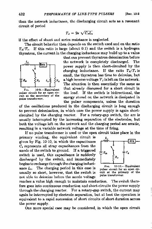
432 PERFORMANCE OF LINE-TYPE PULSERS [SEC.10.3
than the network inductance, the discharging circuit acts as a resonantcircuit of period
Td=%rme
if the effect of shunt and series resistance is neglected.The circuit behavior then depends on the switch used and on the ratio
Td/T,. If this ratio is large (about O.1) and the switch is a hydrogenthyratron, the current in the charging inductance may buildup to a value
that can prevent thyratron deionization beforeLc
m
~~Nthe network is completely discharged. Thepower supply is then short-circuited by thecharging inductance. If the ratio Td/T, issmall, the thyratron has time to deionize, but
~ EM Rp Le Re a high inverse voltage V~ is left on the network.The situation is then essentially the same as
FIG. 10.9.—Equivalent that already discussed for a short circuit inPulserCirctitfOran OmnCir- the load. If the switch is bidirectional, thecuit at the secondary of thepulse transformer. energy stored on the network is dissipated in
the pulser components, unless the durationof the oscillations produced in the discharging circuit is long enoughto prevent deionization, in which case the power supply is again shoficircuited by the charging reactor. For a rotary-gap switch, the arc isusually interrupted by the increasing separation of the electrodes, butboth the voltage left on the network and the charging period are erratic,resulting in a variable network voltage at the time of firing.
If no pulse transformer is used or the open circuit takes place in theprimary winding, the equivalent circuit is ~tgiven by Fig. 10.10, in which the capacitanceC, represents all stray capacitances from the
m
h
anode of the switch to ground. If a triggered ~ ~tiswitch is used, this capacitance is suddenly
8
discharged by the switch, and immediatelyRP
begins to recharge through the charging induc~ante L.. The charging period in this case is ~d~r”~irc~t”~~~~o$nd~~~usually so short, however, that the switch is cuit at the primary of the
not able to deionize before the anode voltage pulsetran8f0rmer.
reaches a value high enough to maintain conduction. The switch there-fore goes into continuous conduction and short-circuits the power supplythrough the charging reactor. For a rotary-gap switch, the current mayagain be interrupted by electrode separation, but at best the operation isequivalent to a rapid succession of short circuits of short duration acrossthe power supply.
One more special case may be considered, in which the open circuit

SEC. 10.3] OPEN CIRCUITS AND PROTECTIVE MEASURES 433
takes place at the primary of the pulse transformer and a long cable con-nects the pulser to the pulse transformer. The equivalent circuit is thengiven by Fig. 10.11, where the cable is considered as a pulse-formingnetwork. The discharging circuit then consists of two pulse-formingnetworks of the same impedance but different pulse durations, connectedin series, which are short-circuited by the switch when it operates. Theresult is then again comparable to that obtained with a short-circuitedload.
Protection of Circuit Elements by Relays.-In line-type pulsers o wer-current, undercurrent, and reverse current relays are used for the pro-tection of circuit elements against load variations, as well as against thepossible failure of some of the elements themselves.
It has been shown that an open circuit inthe load often causes the switch tube to con- Lc
m
PFN
duct continuously. The protective deviceshould therefore be an overload relay in the
.
power-supply circuit. For d-c charging, the s EM Cable
usual practice has been to connect a relay in RV
the ground return of the power supply, thecontacts opening the connections to the pri- FXG. 10.11.—Equivalentmary of the transformer. Undercurrent relays ~~~~t~~~~~~o~~0~~~’~~-in the load are also used for this rmr~ose.
In order to devise effective protection against short circuits in theload it is necessary to consider the type of switch and the nature of thecircuit being used. If the switch is unidirectional and auxiliary circuitsare not included to prevent the buildup of network voltage after a shortcircuit, the average power-supply current increases with the networkvoltage and an overload relay in the grounded side of the power supplywill readily disconnect the primary power input. If bidirectional switchesare used, or if a shurit diode or similar system is used to maintain the net-worK voitage very nearly constant, the average pulser input current isalmost unchanged by the short circuit in the load. On the other hand,the ratio of peak load currents for short-circuit and normal operationusually does not exceed two, and the increase in average load current islarge only if the short circuit in the load is unidirectional. Althoughan overload relay in the load does not operate under certain conditions,it was widely used as long as no better system was available. Protectivedevices whose operation depends on reverse current have proved themost satisfactory.
The first of ~hese devices was designed specifically for use in pulsersemploying shunt diodes. As has been explained above, the shunt diodedoes not normally conduct any current, but, when a short circuit occurs, itcarries the average pulser current. Some device for averaging the diode

434 PERFORMANCE OF LINE-TYPE PULSERS [SEC. 10.3
current must, of course, be used; it can be either a thermal relay, or acapacitance connected in parallel with a magnetic relay. The time con-stants of the available magnetic relays and condensers cannot usuallybe made long enough to delay the operation of the relay for more thanten consecutive short-circuited pulses. Since such rapid action is notnecessary for protection of the components, thermal relays are generallypreferred. Relays are chosen that will operate either after one or twoseconds during which short circuits occur at every pulse, or when therate of sparking in the magnetron exceeds a predetermined limit for alonger time. This limit is determined by the ratings of the shunt diodeand other circuit components. Experience with pulsers used in micro-wave-radar applications indicates that the thermal relay should operatewhen the load is short-circuited on 15 to 25 per cent of the pulses duringa 15- to 30-sec interval. It must be noted that the thermal relay operates
B+ as a function of the effective, not the average,
d
value of the current, and that the ratio of theseR values varies with the design of the shunt-‘2 diode circuit. It must also be pointed out
.—T, that the relay in this position becomes less
Transformer
1
effective if the cathode emission of the shuntdiode decreases.
The second type of reverse-current protec-tion was designed specifically for a spark-gap
.FIG. ~o.lz~~chemati~ pulser, but is applicable to all pulsers using
diagramof a protectivecircuit bidirectional switches. It should not be usedusingreversecurrent. in place of the method desa-ibed above becauseits operation depends on a large peak reverse current, which is not obtainedwith tbe shunt diodes available at present.
The principle of operation is as follows (See Fig. 10.12). The polar-ity of the main pulse current flowing through the primary of the pulsetransformer T is such that, for normal pulses, the cathode of T1 is drivenpositive #ith each pulse. Hence, the grid of Tz is maintained at groundpotential, and a certain current normally flows through R. A pulse ofopposite polarity, however, drives the cathode of T1 and the grid of Tznegative, reduc~g the current through R. The resistance R can easily
be replaced by a relay, and the circuit constants made such that the relayis de-energized when reverse current flows through the transformer forone or several pulses.
The transformer T actually used in one radar system consists of asmall steel ring fitted at the cable connector in such a way that the pulsecurrent passes through the axis of the ring. One turn of wire is loopedaround the ring, and the voltage generated is sufficient to operate theprotective device. Simplifications were introduced in the circuit of

SEC.10.4] NORMAL OPERATION OF THE MAGNETRON 435
Fig. 10.12by eliminating theplate-voltage supply ;tube T*thenacts asagrid-controlled rectifier, and the load consists of the relay bypassed by acondenser. An auxiliary contact introduces an additional voltage onthe grid, which keeps the relay de-energized until a reset button is pushed.This system of protection has proved very satisfactory.
PULSER PERFORMANCE WITH A MAGNETRON LOAD
10.4. Normal Operation of the Magnetron.-This section discussesqualitatively the operation of a pulser with actual magnetron loads, andattempts to point out the difference between operation with a magnetronand with a perfect biased diode. Particular attention is paid to some ofthe characteristics of the magnetrcn which may, under some conditions,
make it an unstable device, and to some of the corrective methods whichhave been used to improve the performance of the over-all transmitter.
The magnetron input characteristics can best be analyzed from astudy of the voltage-current characteristic curves. Some oscillograms ofsuch characteristics are given in Fig. 10.13, the time sequence of thecurves being given by OABCO. Any portion of the curve correspondingto negative voltages is due to post-pulse backswing and need not beconsidered here.
The part of the curve OA corresponds to the buildup of the voltage.In general, only capacitance current is drawn by the magnetron duringthis time, although leakage current may be present in some cases. Thetime necessary for the voltage buildup is usually between 0.05 and 0.2psec, depending on the pulser characteristics. The portion AB corre-sponds to the buildup of current in the magnetron. There is usuallylittle or no increase in voltage corresponding to the current buildup;there may even be a slight decrease. The time necessary for currentbuildup has not yet been measured very accurately, but it is always veryshort and has been estimated to be as low as 5 x 10⁻⁹ sec for some low-voltage X-band magnetrons (2J42). Point B coriesppnds to the so-called

436 PERFORMANCE OF LINE-TYPE PULSERS [SEC. 10.4
“flat” portion of the pulse, where both voltage and current remain con-stant except for small oscillations.
From B to C both current and voltage decay at the end of the pulse,the line BC giving the diode characteristic of the load, which has beenused before. Any slow variations of voltage and current, such as oscilla-tions up to perhaps 10 Me/see, follow very nearly the same curve oncethe magnetron is operating. Corrections may have to be made, however,for the transit time between the plates of the cathode-ray tube or otherviewing-system defects at higher oscillation frequencies. The averageslope of this curve thus gives the dynamic resistance of the magnetron.From C to O, the voltage is gradually decreasing to zero, and againcapacitance current may cause the curve to deviate slightly from theaxis. This deviation is much smaller than that resulting from the volt-
CabtePFN )
PT
1P - ~~ ~ +
Rd
“1 ~. .
FIG. 10. 14.—Line-t ype pulser with a despiking RC-net work.
age buildup, however, because of the much smaller rate of change ofvoltage.
The assumption that the load acts as a biased diode does not holdduring the starting period of the puke after the voltage has reached anamplitude corresponding to C. It can be assumed, however, either thatthe magnetron impedance is intinite until the voltage reaches a value A,
and then drops suddenly (in about 10–s see) to the normal operatingvalue, or that during the buildup of oscillations, that is, from points Oto B, the magnetron is a biased diode of nearly zero internal resistance.
The value of the voltage at A is, unfortunately, not constant, butdepends to some extent on the time required for the voltage to build up{O this value. Hence, no general analysis of the problem can be made.It can be stated, however, that the sudden rush of current through the‘load tends to produce unduly high oscillations by means of the shockexcitation of the LC-circuits in the pulse transformer connecting the pulserto the load.
One satisfactory method of decreasing the resulting mismatch is tointroduce an RC-circuit in parallel with the primary of the transformer,as shown in Fig. 10.14. Its purpose is to minimize the “spike” that oftenappears at the beginning of both voltage and current pulses because of

SEC. 10.4] NORMAL OPERA TION OF THE MAGNETRON 437
the magnetron characteristics discussed above. If a unit function ofvoltage is applied to the despiking network, its instantaneous impedanceas a function of time is given by
zd = R.&l Racd.
The instantaneous impedance that the pulse transformer presents to aunit voltage until the magnetron starts to oscillate is a complicatedfunction of time. A satisfactory approximation can be obtained, how-ever, by reducing the pulse transformer to its leakage inductance anddistributed capacitance, L. and C., respectively. Its instantaneousim~edance can then be expressed as
The effect of the despiking RC-cir-cuit - on the instantaneous outputimpedance of the pulser can best beseen by a graph such as that of Fig.1015. For the sake of uniformity,the instantaneous output imped-ances are referred to the networkimpedance ZN, and the followingassumptions are made,
and
<Z,c,; = &d:.t/R#cd
Fto. 10.15.—Instantaneous output im-pedances of a pulser with a despiking RCnetwork,
The time scale can then be t/RdCd,and the impedance scale z/ZN. Thecurve zr/Z~ is the pulse-transformer instantaneous impedance, andobviously starts at infinity. ‘I’he resulting instantaneous mismatchproduces a reflection of voltage to the pulse-forming network through thecable linking the pulser to the load, and further reflections at the network-cable junction may produce undue oscillations in the load voltage.
The instantaneous impedance to which the pulser is connectedwhen a despiking RC-circuit is used in parallel with the pulse-trans-former primary is given by
1.=Zi
:+;.

438 PERFORMANCE OF LINE-TYPE PULSERS [SEC.105
When the curves zN/Zd and ZN/Z. are plotted and added graphically,Z,V/zi is obtained. The reciprocal of ZA,/zi is then taken, giving theinstantaneous impedance of the load for the constants used. It canreadily be seen that, for the particular example treated, the values ofzi do not vary from Z~ by more than 13 per cent for any time t < 2.75RdCd.In practice, the magnetron usually starts to conduct before the current inthe leakage inductance of the pulse transformer has decreased to 70 percent of its peak value (corresponding to t = 3R,iCd in this scale). Atthat time, the simplified equivalent circuit considered here is no longervalid, and matching of the load to the pulse-forming network is assuredby.the magnetron itself.
This method of eliminating instantaneous mismatch has been usedextensively with very good results. It has the further advantage oftending to decrease the voltage rate of rise at the magnetron before theoscillations start, since the instantaneous voltage applied to the input ofthe pulse transformer is given by
ZiVi= V,V—
Zi + Z,V”
At the first instant, Vi = V,v if no despiking circuit is used, and v, = V,v/2if a despiking circuit containing h% = Z.V is used. The disadvantage ofthe despiking circuit is a power loss in the additional capacitance Cd,which can be estimated by the method described in Sec. 7.3, and theintroduction of two additional elements in the pulser circuit.
10.5. Magnetron Mode -changing. -Some magnetrons, unfortunately,do not always operate in the intended mode of oscillation once the voltageis applied. The reasons are obviously outside the scope of this chapter, 1but, since remedial measures can be introduced in the pulser to preventsome magnetrons from selecting the wrong mode of oscillation, a briefexplanation of some possible mode-changing processes is given here. Acommon type of mode change from pulse to pulse (called mode-skipping)may be most readily understood by a study of the voltage-current charac-teristics of a magnetron exhibiting such behavior. Figure 10.16 showsoscillograms of the voltage-current input to a magnetron that is skippingmodes. First, it may be noted that the operating characteristics of theunwanted mode are such that the voltage is higher and the current lowerthan the values corresponding to the normal mode of operation. Ofparticular interest is the fact that mode selection is determined at thevery beginning of the current pulse. Looking at the voltage rise, it isseen that, at a point corresponding to .4 of Fig. 10.13, the magnetroncurrent tends to increase, but succeeds in reaching the operating point
I See Vol. 6, Chap. 8,

r
I
I
SEC.105] MAGNETRON MODE-CHANGING 439
only occasionally. In other cases, the voltage continues to increase untilthe current starts to build up the oscillations in the unwanted mode.
For the purpose of this section, it is suficient to say that a mode skipcan take place if the voltage applied to the magnetron is allowed to reach aregion in the V-I plot where the unwanted mode may start.
Obviously, if the voltage is neve; allowed to reach the region whereinstability may develop, the problem of mode-skipping does not arise.By increasing the voltage-rise time through the region where the magne-tron starts in the desired mode to a value greater than the magnetron-starting time, the voltage can be kept out of the region of instability.
-
I
z—
(a) First tube. (b) Second tube. (c) Idealizedsketch;time.. . . ..Iouows arrows; ~ r.e menormal operating mode; Bie the unwantedmode.
FIG. 10. 16.—V-I Characteristics of mode-skipping magnetron.
This condition alone is not necessarily sufficient, however, since themagnetron-starting time itself may vary, depending on the voltage rate ofrise itself, and possibly on pulser circuit conditions.
The increase in voltage-rise tim~r decrease in the rate of rise ofthe voltage-can be accomplished, as explained before, by addition of adespiking RC-circuit in parallel with the pulse-transformer primary.It can be achieved, however, more simply and directly by adding eithera capacitance in parallel with the magnetron (increasing CD) or aninductance in series with the pulse-forming network and the pulse trans-former (increasing LD). If the simplified puke-transformer circuit isconsidered, an increase in either of those quantities by the same per-centage should have very nearly the same efiect on the front edge of thevoltage pulse. Experimental results agree with this conclusion, but alsoindicate that the tendency to skip modes is not always afiected in the

440 PERFORMANCE OF LINE-TYPE PULSERS [SEC.10.5
same way by a given decrease in rate of rise of voltage if this decrease is aresult of additional inductance rather than additional capacitance.
For the 2J42 magnetron, for example, a greater decrease in dv/dt isnecessary in order to bring about the same proportional reduction inmode-skipping if an inductance is used. This result can be explained bya consideration of the instantaneous impedance of the pulser output cir-cuit and of the time necessary for current to build up in the magnetron,
(a) L = O.
(b) L = 5jdL
(C) L = 15ph.FIG. 10. 17.—Magnetron voltage and
current Pulses (lower and upper traces r~spectively) showing the effect of seriesinductance between the pulse transformerand the pulse-forming network.
which has been estimated to be aslow as 0.005 ysec for some of thesemagnetrons.
Additional capacitance in par-allel with the magnetron has twoeffects: (1) it increases the maxi-mum value of current in the leakageinductance of the pulse transformer,and (2) it stores added energy inparallel with the load. The com-bined result is that a greater instan-taneous current can be supplied tothe load. Additional inductance inseries with the pulse-transformerleakage inductance, on the otherhand, decreases the maximum in-stantaneous current flowing throughthat inductance. Hence, less cur-rent is available to permit the mag-netron to start in the desired mode,and a very much larger decrease involtage rate of rise is necessary be-fore the tendency to skip modescan be corrected.
In practice, however, a capaci-tance cannot alwavs be chosen that
will correct for mode-skipping in magnetrons. The principal objectionto the use of a capacitance in the circuit is the resulting decrease in pulseduration and efficiency. Series inductance generally tends to lengthenthe pulse duration and to decrease the efficiency by a smaller amount.The amount of inductance used, however, must not be so large that theshape of the current pulse deteriorates appreciably. Figure 10.17 is anexample chosen at random from many photographs showing the mag-netron voltage and current pulses (lower and upper traces respectively)as a function of added inductance. For all these pulse photographs,V, = 5.4 kv and 11 = 4.5 amp, ‘The rate 01 rise of voltage was reduced

SEC. 10.6] MAGNETRON SPARKING 441
from 59kv/~sec (Fig. 10.17a) to46kv/~sec (Fig. 10.17b) bythe additionof a fi-ph inductance in series with the network and pulse transformer,and to 40 kv/~sec (Fig. 10”17c) by a 15-Ph inductance. Actually, amarked improvement in current pulse shape is observed between Figs.10.17a and b but the slope of the current in Fig. 10.17c is detrimentalto the r-f spectrum.
Other types of mode changes may be possible in magnetrons. Insome cases the magnetron may be able to operate in an unwanted modethat starts at a voltage lower than that of the desired mode. A possibleremedy may then be to decrease the time of rise of the voltage throughthe starting region for the unwanted mode to a value lower than the start-ing time for that mode by increasing the number of sections in the pulse-forming network and reducing the leakage inductance and distributedcapacitance of the pulse transformer. Finally, mode-shifting-or achange in operating mode during a puls~may occur. In general, littlecan be done to the pulser to prevent this behavior.
10.6. Magnetron Sparking.-Sparking difficulties have occurred fre-quently in the magnetrons used in radar systems, 1principally because ofthe war-imposed necessity of rating the operating point of the tubes withan insufficient factor of safety. The following discussion summarizesthe present knowledge of the effect of line-type-pulser characteristics onmagnetron sparking, as well as the effect of magnetron sparking on pulseroperation. The experimental study of the causes and effects of sparkinghas been conducted primarily on a statistical basis. Some pictures ofindividual current and voltage pulses during sparking are shown inFig. 10.18. These records were taken on a rapidly moving film in orderto obtain the desired separation between pulses, and the blur in thepictures is caused by the persistence of the fluorescent screen of thecathode-ray tube. Figure 10.18a shows a series of voltage pulses from amedium-power magnetron, Fig. 10.18b shows current pulses on the samemagnetron, and Fig. 10.18c current pulses on a high-power magnetron.The line drawings in Fig. 10.19 show schematically the conditions occur-ring in a few of the oscillograms of Fig. 10.18. The immediate conclu-sions that can be drawn from observation of the individual pulse picturesare:
1. Sparks may take place at any time during the pulse.2. A spark can be initiated in several ways, corresponding in some
cases to a rapid “ncrease in current to almost twice the normalvalue, and in some cases to a reasonably slow breakdown of voltageand increase in pulse current.
1 See Vol. 6, Chap. 12.

442
3.
PERFORMANCE OF LINE-TYPE PULSERS [SEC.10.6
After the spark is initiated, it can have the character of an arc
(as indicated by pictures in which the voltage stays very nearlyzero), or it can show unstable characteristics, possibly caused byoscillations in the external circuit. These characteristics are shownby pictures in which the voltage trace at the zero axis is broken,
indicating temporary high potentials between anode and cathodeafter which the spark again breaks down the cathode-anode space.
magnetron. magnetron. magnetron.FIG. 10. lS.—Oscillograms showing the effect of magnetron sparking on voltage and
current pulse shapee. The first trace in each series is a normal pulse.
There are many causes for the initiation of a spark in the magnetron,as evidenced by oscillograms similar to those shown here. In some cases,the spark is presumably caused by bursts of gas in the magnetron. Avery high percentage of sparks occurs in some tubes during pulses when

SEC.10.6] MAGNETRON SPARKING 443
the magnetron is operating in an unwanted mode at a higher voltage anda lower current than the nprmal values. In other cases, sparking ispresumably associated with cathode fatigue during the pulse;1 manyphotographs of individual voltage traces indicate that the currentdecreases and the voltage rises slowly (in a few tenths of a psec) to avalue that is 10 to 20 per cent greater than normal before the tubebreaks down.
The assumptions made in the study of the effects of sparks on pulseroperation should cover a wide range of possibilities. The variable natureof the sparks—from an almost perfect short circuit to a very nearlynormal pulse-result in values of K (the mismatch coefficient) rangingfrom – 1 to O, if the losses in the circuit areneglected.
For pulsers using bidirectional switches,the protective systems described in Sec. 103 ware satisfactory; for pulsers using unidirec- (a) Voltagepulse.
tional switches, a diode circuit in parallel withthe pulse-forming network has proved to bcparticularly effective. The effectiveness ofthe shunt-diode circuit depends to a certainextent, however, on the value of K. A typi-
Wcal example has been worked out using the (b) Current pulse.general method outlined in Sec. 10.2, and the FIG. 10.19.—Schematicmost significant results are given in Figs. representation of the pulse
10.20, 10.21, and 10.22.2 The circuit con-shapesof Fig. 10.1S.
stant.s are those of a medium-power airborne pulser, rated at 200-kw pulse-power input to a 4J52 magnetron, with pulse durations ranging from 0.25to 5.4 usec. Since sparking was most prevalent for the long pulses, thefollowing values of parameters were used:
Charging inductance L. = 16 henrys,Charging circuit Q =” 15,Network capacitance C.v = 0.0525 pf.
For the study, a range of values were considered for the shunt-diodecircuit. Figure 10.20 shows some typical charging waves for normaloperation and after a spark (K = —0.8) for several values of the shunt-diode circuit parameters Fig. 10.20a shows the first part of the chargingwave on an expanded time scale. Figure 10.21 gives the percentageincrease of network voltage over its normal value as a function of themismatch coefficient for several combinations of series induct ante and
1Volume 6, Chap. 12.
z O. T. Fundingshmdand Anna Wnltcr, “ Annlysisof I.inr hlmiulator Behaviorwith a SparkingMngnct.ronImad.” RI, Report No. 765, .\ug. 10, 1945.

444 PERFORMANCE OF LINE-TYPE PULSERS [SEC.10.6
resistance in the diode circuit. At first glance, the circuits containinginductance seem highly preferable because they maintain the networkvoltage nearer to the normal value, and can be designed to produce areduction in this voltage.
t in Asec
FIG. 10.20.—Computed charging waves for normal sndsparking operation of the Iowi.Circuit constants:L. = 16 henrys, R, = 1200011111s,Q = 15, C’N =0.0525pf. CUrve (I):Normal operation, K = O. Curve (2): Sparking operation, K = –0.8, no shunt diodrcircuit (R.g = m). Curves (3) and (3a): Sparking operation, ~ = –().&, R.s = 2000 ohms.Ls = O. Curves (4) and (40): Sparking operation, K = –0.8, Rs = 700 ohms. L.s = 45mh.
If an RL-circuit is used to obtain negative regulation (that is, adecrease in the network voltage from normal after a spark), the instan-taneous power-supply regulation may be such that the second pulwfollowing the spark is higher than normal, and the advantage of the goodinitial regulation is thus lost. This high pulse occurs bccnuw the current,drain from the power supply is smaller during the charging pmi[d thatproduces a network voltage smaller than norsmd, and thus leaves a higher
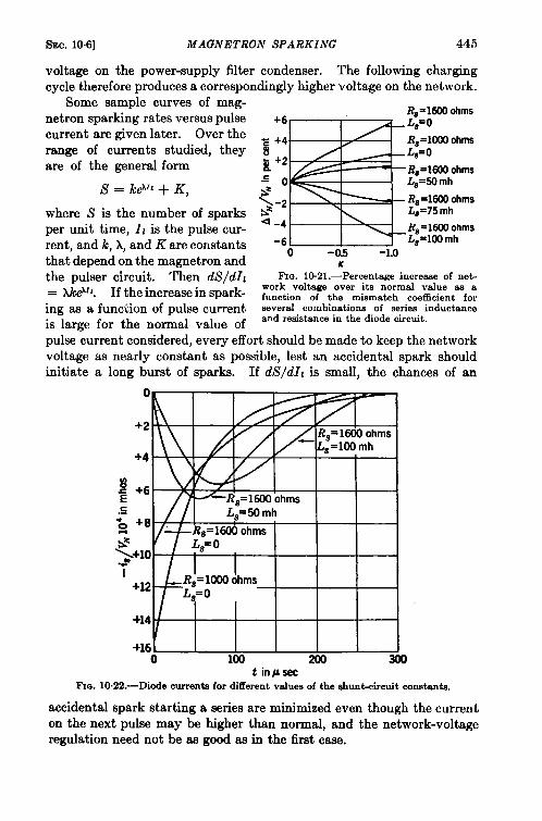
SEC.10.6] MAGNETRON SPARKING 445
voltage on the power-supply filter condenser. The following chargingcycle therefore produces a correspondingly higher voltage on the network.
Some sample curves of mag-Rs=1600ohms
netron sparking rates versus pulse +6
@
La=Ocurrent are given later. Over the = +4 R8=1000ohmsrange of currents studied, they s La=Oare of the general form ~ +2
% R&=1600ohms.E o
8 = ke”’ + K,L~=50 mh
$-2 Rs=1600ohmswhere S is the number of sparks La=75 mh
a.4per unit time, 11 is the pulse cur- R~=1600 ohms
rent, and k, X, and K are constants -6 L~=100mh
that depend on the magnetron ando -0.5 -1.0
Kthe pulser circuit. Then dS/dlt Fm. 10.21.—Percentage increase of ne~
= ~~lz. work voltage over its normal value as aIf the increase in spark- function of the mismatch coefficient for
ing as a func~ion of pulse current severul combinations of series inductance
is large for the normal value ofand resistance in the diode circuit.
pulse current considered, every effort should be made to keep the networkvoltage as nearly constant as possible, lest an accidental spark shouldinitiate a long burst of sparks. If dS/dIl is small, the chances of an
o
+2
+4
8c +6Ec.-
*Z +8
<+10---I
+12
+14
+160 lm 200 300
t in~secFIG. 10.22.—Diode currents for different values of the shuntiircuit constants.
accidental spark starting a series are minimized even though the currenton the next pulse may be higher than normal, and the network-voltageregulation need not be as good as in the first case.

446 PERFORMANCE OF LINE-TYPE PULSERS [SEC. 10.6
Another item to be considered is the peak current in the shunt diode.Figure 10.22 shows the diode currents for the shunt-circuit constantsconsidered and for K = – 0.8. It is seen here that the peak currents indiode circuits using series inductance are much smaller. Finally, someconsideration must be given to the switch-tube deionization. Asexplained in Chap. 8, it may be helpful to maintain some inverse voltageon the plate of a thyratron for some time after the pulse. When such isthe case, the time constant of the shunt-diode circuit must not be so
1~50 60 70 60 90
Currentin ampFIG. 10.23.—Sparking rate vs. cur-
rent for variable pulse durations. Inall cases, do/dl = 200 kv/psec at 60amD.
Currentin ampFIG. 10.24.—Sparking rate vs. current for
different networks of identical pulse durationand variable dv/dt.
Network 1: du/dt = 307 kv/Psec at 70 amp.Network 2: dv[dt = 252 kv/psec at 70 amp.Network 3: duldi = 20S kv /usec at 70 ammNetwork 4: dv)dl = 175 kv~psec at 70 am&
short that the normal inverse voltage is removed before the thyratron iscompletely deionized, lest continuous conduction result.
The effect of the pulser circuit on the magnetron sparking rate in aparticular case was studied experimentally by means of electronic sparkcounters, and by varying the pulser parameters one by one wheneverpossible. The most reliable data have been obtained on high-powerS-band magnetrons,l and the results, insofar as they may affect pulserdesign, are given in Figs. 10.23, 10.24, and 10.25. An exponential curvefits the data obtained for sparking rate as a function of pulse current.It can also be seen that an increase in pulse duration and an increase inrate of rise of voltage both increase the sparking rate. In general, the
I H. L. Rehkopfand R. E. Nysewander,“Sparkingof HK7 Magnetronsaz a Func-tion of Pulse FormingNetwork,” RL InternalReport 51-9/24/45.

SEC. 106] MAGNETRON SPARKING 447
pulse duration and the pulse current are determined by the systemrequirements, and the designer of the pulser for the system has little or nocontrol over these quantities. Changes in voltage rate of rise may beintroduced, however, as long as the pulse shape is not affected to theextent that the r-f spectrum becomes unacceptable. For this particularmagnetron, the sparking rate can be reduced by a factor of 10 if the rateof rise of voltage at the magnetron is decreased from 300 to 200 kv/~sec.
Some magnetrons, however, tend to operate in a high-voltage mode ifthe rate of rise of voltage is low, and, as has been indicated, the change inmode is often accompanied by sparking. The possible result is indicated
.G~ lCQ— / /
I /x /. 70amp /~
/
%3 / ‘
160 amp
g 10 /E /
s /
/ ‘
1.0
160 200 220 240 Xa 280 3ofJRate of rise of voltage in kv/A sec
FIG.10.25.—Sparking rate vs. rateof rise of voltage for several pulse cur-rents at r = 1.89psec.
FIG,10.26.—Sparking rate vs. rate ofrise of voltage (average of six 4J52 magne-trons).
by Fig. 10.26, which shows the average trend of sparking rate for sixmedium-power X-band magnetrons (4J52) as a function of rate of rise ofvoltage at a constant pulse duration and pulse current. It is seen, inthis case, that the value of dv/dt cannot be decreased indiscriminately inorder to minimize sparking.
If the rate of rise of voltage is decreased by connecting a capacitance inparallel with the magnetron, the sparking rate may be increased insteadof decreased, presumably because of cathode phenomena in the magne-tron. For normal operation of a line-type pulser the short-circuit cur-rent does not exceed twice normal value, but, if a capacitance is connectedacross the magnetron terminals, the instantaneous current produced bythe discharge of that capacitance when a spark occurs may be manytimes the normal current. This high current may, in turn, damage thecathode to a point where the probability of a spark occurring on thefollowing pulse is much greater than normal, resulting in a long burst ofsparks.
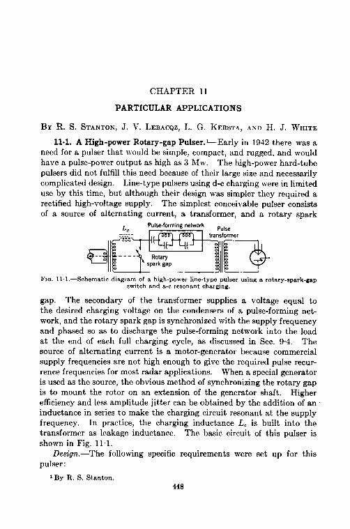
CHAPTER 11
PARTICULAR APPLICATIONS
BY R. S. STANTON, J. V. LEBACQZ,L. G. KERSTA, AND H. J. WHITE
11.1. A High-power Rotary-gap Pulser. I—Early in 1942 there was aneed for a pulser that would be simple, compact, and rugged, and wouldhave a pulse-power output as high as 3 Mw. The high-power hard-tubepulsers did not fulfill this need because of their large size and necessarilycomplicated design. Line-t ype pulsers using d-c charging were in limiteduse by this time, but although their design was simpler they required arectified high-voltage supply. The simplest conceivable pulser consistsof a source of alternating current, a transformer, and a rotary spark
~fq- ,~ ~
FIG. 11. 1.—Schematic diagram of a high-power line-type pulser using a rotary-spark-gapswitch and a-c resonant charging.
gap. The secondary of the transformer supplies a voltage equal tothe desired charging voltage on the condensers of a pulse-forming net-work, and the rotary spark gap is synchronized with the supply frequencyand phased so as to discharge the pulse-forming network into the loadat the end of each full charging cycle, as discussed in Sec. 9.4. Thesource of alternating current is a motor-generator because commercialsupply frequencies are not high enough to give the required pulse recur-rence frequencies for most radar applications. When a special generatoris used as the source, the obvious method of synchronizing the rotary gapis to mount the rotor on an extension of the generator shaft. Higherefficiency and less amplitude jitter can be obtained by the addition of aninductance in series to make the charging circuit resonant at the supplyfrequency. In practice, the charging inductance L. is built into thetransformer as leakage inductance. The basic circuit of this pulser isshown in Fig. 11.1.
Design.-The followingpulser:
IBy R. S. Stanton.
specific requirements
448
were set up for this

SEC.11.1] A HIGH-POWER ROTA R Y-GAP PULSER 449
Pulse power output: 3 Mw.Pulse duration: 0.9 psec.Recurrence frequency: 400 pps.Load impedance: 50 ohms.
Supply voltage: 220 volts, 3 phase, 60 cycles/see.The quantities important to the pulser design are obtained from theserequirements and from the relationships between the various pulser param-eters that are developed in the preceding chapters.
The pulse voltage for a 50-ohm load is
Vl=m=d 3 X 10’ X 50 = 12.3 kv,
where P; is the pulse-power output and Z1 is the load impedance. Whenthe network impedance is equal to 50 ohms, the total capacitance of thenetwork becomes
c. = & = 0.009 pf,
and the network voltage is
‘N=e=2x3:.::xm”265kv
where ~d, the efficiency of the discharging circuit, is assumed to be 85per cent. The average power taken from the network is given by
~N = ?kfr _ 3 x 106x 0.9 x 10-’ x 400—_?ld 0.85
= 1260 watts.
Choosing full-cycle charging (n = 2, P = 900), the secondary voltage ofthe charging transformer, from Eq. (9.66), is
VN
For an assumed value of Q = 12,
Eh =0.707 X 26.5 X 103 = 6,8 kv
r 912(1 – e-~)
and the current in the transformer secondary, obtained from Eq. (9.94),is
1- =nirC~EWa
21/G ‘

450 PARTICULAR APPLICATIONS [SEC.11.1
where Eb is the peak applied voltage. For this example,
I- =lf(o.oo9 x 10–6) @(6.8 x 10³)(27r x 400) ~ 0285 amp,
Wso
Eh X I- = 1940 volt-amp.
The average current is obtained from Eq. (9.95);
The charging inductance is given by
L.=&=a (0.009 x lo~’)(k x 400)’ = 17”4 ‘envs”
Although this value is the total necessary inductance, the source induct-ance, transformed by the square of the transformer turns ratio, must be
FIG. 11 .2.—High-power Iin&type pulser of Fig. 11.1, side view,
considered when designing the transformer because it supplies an appreci-able part of this total. In this high-power pulser, the source inductanceis approximately 0.001 henry, and the equivalent secondary inductanceis about 3.5 henrys. With the usual circuit Q, the value of the resonatinginductance is not critical, and it can vary + 5 per cent without seriouslyaffecting the operation.
Description.-The motor-generator and rotary gap are mounted onvibration-absorbing mounts in a small framework. The contactor box
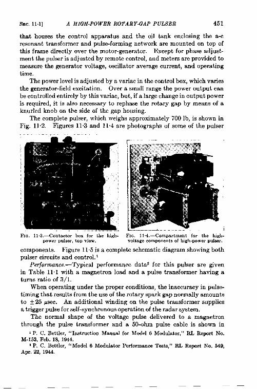
SEC.11.1] A HIGH-POWER ROTARY-GAP PULSER 451
that houses the control apparatus and the oil tank enclosing the a-cresonant transformer and pulse-forming network are mounted on top ofthis frame directly over the motor-generator. Except for phase adjust-ment thepulser isadjusted by remote control, andmeters are provided tomeasure the generator voltage, oscillator average current, and operatingtime.
The power level is adjusted by a variac in the control box, which variesthe generator-field excitation. Over a small range the power output canbe controlled entirely by this variac, but, if a large change in output poweris required, it is also necessary to rephase the rotary gap by means of aknurled knob on the side of the gap housing.
The complete pulser, which weighs approximately 700 lb, is shown inFig. 11.2. Figures 11.3 and 11.4 are photographs of some of the pulser
-—. .. .-.
c: —--- .. .... .. – – .-&-
I
FIG. 11 ,3.—Contactor box for the high- FIG. 11.4.—Compartment for the high.power pulser, top view. voltage components of high-power pulser.
components. Figure 11.5 is a complete schematic diagram showing both
fmlser circuits and control. 1
Performance. —Typical performance data2 for this pulser are givenin Table 11.1 with a magnetron load and a pulse transformer having aturns ratio of 3/1.
When operating under the proper conditions, the inaccuracy in pulse-timing that results from the use of the rotary spark gap normally amountsto t 25 psec. An additional winding on the pulse transformer suppliesa trigger pulse for self-synchronous operation of the radar system.
The normal shape of the voltage pulse delivered to a magnetronthrough the pulse transformer and a 50-ohm pulse cable is shown in
‘ P. C. Bettler, “Instruction Manual for Model 6 Modulator,” RL Report No.M-153, Feb. 18, 1944.
~ P. C. Bettler, “ Model 6 Modulator Performance Teats,” R.L Report No. 549,Apr. 22, 1944.

452P
AR
TIC
UL
AR
AP
PL
ICA
TIO
NS
[SE
C.11.1
1,<I
7-”1!I
III
uIu
:lllllI
iIi;
1-——
— JI
K#l
II
r–––––-.-
1i!
,-++---+In
~--l.l“’”’
1[
IIIIIIII1II!:
IILA-
d%L–--––-.-J
(.--——
——
——
——
d*

SEC. 11.1] A HIGH-POWER ROTA R Y-GA P PULSER 453
‘TABLE11.1.—TYPICAL PEItFORMAXCE DATA FOEA HIGH-POWEIiROTARY-GAPPUL.SER
Testso.
123
sup-Generator Pulse-forming
ply-line klagnetron inputoutput
powernet work
P.9, VG-, P,, VN, f’ N, V1, IL.., V1Z,mv, PI,
watts volts watts kv watts kv ma watts M.—
1225 68 535 15.5 505 25 8 12 3 313 0.991680 85 855 19 4 762 28 9 18.0 .520 1 532090 98 5 1135 21.9 1010 31.8 22.4 712 2 11
I C)vr.r-all pukcr eflicierrcy,,u)spr ~ficirlcY I f magnptrcnrom motor generator to
TmtNo,
VL I,.vx I00,
2LV X 100, pc>rcent\ l~Cr (’cnt P.r
1 59 262 62 313 63 34
Fig. 116. The PIIIW rate of rise is t(m steep for certain magnetrons andcwmv modr-changing. In these cases, plllse shape is usually modifiedby means of “ despiking” compo-nents in the mltput circuit, .4 typi-cal circuit for this purpose consistsuf a 12-mh inductance in series \viththe olltp(lt (at the input to the pulsecable) and a 1600-PPf capacitance inseries \\.ith a ,50-ohm nonindllctive
rrsistancr ct)nnwtcd in parallel \vithtlw primar,v of the p[llse transformer.:1 Imttcr solution lYOUICIbe to sub-stitlltc a net\vork that JYaSdesignedto dclil-cr a p\Ilse to fit the particulartype of magnetron used, but this
w t——FIG. 11.6.–-Voltagpulsese shape from
the high. power pulficr of I’ig. 111, A is90 per rent of the average pulse ampli-tude, B IS the arcragc pulse amphtude.
prt)cftlllrr is (IsIIally impractical in a general-p~lrpose pulser.This higll-lolt:lge rotary-gap pldser has been IIsed extensively for
componvnt dcvt,loprnent, life-testing, and magnetron-seasoning. Forthese uses 110alterations \verenecessary except a modification of the out-p~lt pulse shape in order to adapt it to particular magnetrons. This

454 PARTICULAR APPLICATIONS [SEC, 11.2
pulse generator also served as the system field-test pulser for several ofthe modern ground-based microwave-radar systems.
11.2. A High-power Airborne Pulser. ‘—The pulser described in thksection* was designed to supply a pulse power of 600 kw to a 4J50 magne-tron at a duty ratio of 0.1 per cent. Since the pulser was intended forairborne use, it was imperative to keep the weight and size of the packageas small as was compatible ~vith a reasonable operating life, and it wasalso necessary to provide an airtight housing, which introduced additionalelements to be considered in the design. Accordingly, in addition toelectrical design and performance, the following discussion includes abrief outline of mechanical design ~vith particular reference to the prob-lems of heat dissipation. The completed pulser weighed less than 100 lband had an over-all efficiency (including blower and control circuits)of about 40 pcr cent.
l~lec.rical Design J?equircmenLs.—Thc specific requirements for this
pulser were as follolvs:
Pulse-poivcr autput at full-poJver operation: 600 kw (22 kv at 27 amp).I’ulsc-polver output at reduced power (starting): 400 kw (21 kv at 19
amp).Pulse durations: 0.5 and 2.5 ysec.Rccurrcncc frcqucncics: 2000 and 400 pps.Supply voltages: 115 vat 400 to 2400 cycles/see and 24 v d-c.
The requircrncnts of multiple values of pulse duration, recurrencefrequency, and pulse-power output made it necessary to use the mostfhxible circuit possible. Accordingly, d-c inductance charging with abold-off diode and a hydrogen-thyratron s\vitch was chosen. A pulse-forming-network impmlancc of 50 ohms ]vas adopted.
Voltage on the l’ulsr-,/ovmirlq Network and Switch.—If the dischargingcfficicncy, m, is assumed to be 75 per cent, the peak forward pulse-form-ing-network voltage is given by
“.=f+ =2JWX103=126’VSince this value is \vcll ~vithin the specifications of the 5C22 hydrogentbyratron, this tube was then selected as the s~vitch.
Network Capacitance.-The approximate network capacitance isgiven by
CN . &N.
1By J. V. Lebacqz.zS. Siegel,A. I’. ]{ruper, and H. L. Glick, WestinghouseResearchReportSR-316,
Nov. 1, 1945.
SEC.11.2] A HIGH-POWER
For the O.5-psec pulse,
AIRBORNE PULSER 455
c., = 0.5 x 10-’100
= 5000 lwf,
and for the 2.5-Wsec pulse,
Charging Inductance. -In order to insure the best operation of the5C22 at 2000 pps, nearly resonant charging should be achieved. Then
f, = l/T 4L@~, and
L,=~=1
= 5 henrys,~2r,c’N, 1OX4X5X1O–3
which is the value of charging inductance used in this pulser.Shunt-diode Circuit.—In order to maintain a constant peak forward
voltage on the network after an accidental short circuit in the load, it isnecessary to dissipate the inverse voltage left on the network after such ashort circuit as rapidly as possible by means of a shunt-diode circuit acrossthe network. For maximum effectiveness, the time constant of the net-work capacitance and resistance of the shunt circuit should be as small aspossible compared with the charging period. Since most magnetronsparking takes place with long pulses, the charging period to be consideredis
T. = T =, = 1100 psec.
In general, the diode circuit proves reasonably effective if its timeconstant is about 1 per cent of the charging period. Then
RsC~, = 11 X 10-’,~~ = 11 x 10-~
25 X 1O–9= 45o ohms.
A resistance of this value can be obtained by using two 3B26’s in parallel,each in series with a 500-ohm resistance. The maximum ratings of thetubes are not exceeded because, for the peak inverse voltage of 13 kv(rating = 15 kv), the peak current after a complete short circuit is~ 13000/900 = 7.2 amp, and decreases in 5 ~sec to less than 4.5 amp(rating = 8 amp). For a continuous short circuit only the rating forplate dissipation is exceeded. This excess dissipation can be correctedby the protective relay discussed later.
Power Supply.—The power supply was designed as a standard full-wave rectifier with a choke input filter to minimize the effect of the input-voltage waveform on the pulser output. The d-c voltage required fornormal operation can be arrived at by the use of an estimated charging

456 PARTICULAR APPLICATIONS [SEC.11.2
ratio; 1.85 was chosen. Then
EM=$5=~=6.8kv.
For starting,
The average current from the power supply is approximately
Z..v =P1 600
J%x~dx~.= 6800 X 0.75 X 0.925 = 126 ‘a’
or
I..v = C~VNj, = 5 X 2000 X 12.6 X 10–6 = 126 ma.
A total of eight output voltages was provided, in two groups of four.Each group was given by two taps connected near one end of the primarywinding to allow for the change from low (starting) to high (running)power. For each operating power level, four adjustments were providedover a voltage range of approximately ~ 5 percent in order to accommodatepossible variations in the 4J50 input requirements from tube to tube, aswell as to compensate easily for changes in input-voltage waveform.
No particular difficulties were encountered with the power supply,with the possible exception of the filter inductance. Because of thewaveforms supplied by aircraft generators, the peak voltage across theinductance was, for some conditions, greater than 1.5 times the expectedvalue for a sinusoidal voltage. Both the insulation stresses and the coreloss were therefore increased, and the design required special care.
Hold-off Diode.—The maximum expected peak current through thecharging circuit occurs for the long pulse duration and is given approxi-mately by
I Z., =~X126X% %=400 ma.
Since the 705A diode satisfies both the peak- and average-current require-ments in addition to the voltage requirement for the hold-off diode, it wasused in this position as well as in the rectifier.
Pulse-duration S~”tching.-When the pulse duration is changed, it isnecessary to shut off the high-voltage supply for a short time before,during, and after the switching operation in order to prevent the buildupof excessive voltage on the network and to eliminate sparking at theswitch contacts. In this particular instance, two auxiliary relays (K5and KT) actuate the main connector relays Kj and Ko as well as thehigh-voltage network switch (K,), designed especially on a Rototrolmechanism. (See Fig. 11.7.) The main power supply is cut off before

SEC. 11.2] A HIGH-POWER AIRBORNE PULSER 457
the pulse duration is changed, and the power is restored m soon as thehigh-voltage switch is again in operating position.
Protection. —Protection against short circuits in the load is normallyachieved by the shunt-diode circuit, which prevents dangerous overvolt-ing of any pulser component and keeps the average current very nearlyconstant. For prolonged short circuits, it is desirable either to turn offthe pulser, or at least to change its output from high to low power. Sincethe largest current change resulting from a fault occurs in the shunt-diode circuit, a protective relay is introduced in this circuit. A thermalrelay ( TK1 of Fig. 11“7) was selected for this function because of itslong operating delay. The relay chosen in this particular case operatesin approximately one second in case of a short circuit in the load (seeSec. 10.3), but takes five seconds to return to its normal position. Theresultant decrease in the average plate dissipation in the diode to onesixth of the expected value enables the 3B26 to be operated within ratings.
The pulser components are protected against the effects of an opencircuit in the load, or a short circuit across the power supply caused by afault in the pulser, by means of an overload relay (K, in Fig. 117).This relay is of the “flapper” type, and releases when the high voltage isshut off. When the trouble condition is continuous, tinal protection isassured by overloading the fuses through the resistance RI.
Trigger Ampli$er.-The trigger pulse supplied by the radar system tothe pulser may vary in amplitude from 7 to 150 volts, and in durationfrom 0.5 to 10 psec. Because of the trigger and bias requirements of the5C22 hydrogen thyratron, a special power supply was needed for its gridcircuit. The trigger amplifier is shown in Fig. 11.7. A double triode isused, one half of which serves as an amplifier and limiter, and the otherhalf as the tube in a regenerative pulser. The trigger pulse for the 5C22is obtained from the cathode-follower output from the regenerative pulsertube.
Insulation.-All magnetic components used in this pulser have beendesigned with Fosterite insulation in order to reduce their weight to aminimum and to enable operation at ambient temperatures bigher thanthose that standard equipment would normally withstand. Results sofar have been very satisfactory. It was also desired to use diaplex asnetwork insulation to further reduce the weight. Because of coronadifficulties occurring at the operating-voltage levels, a satisfactory diaplexnetwork was not available, and a network with oil-impregnated paperinsulation was used instead. By careful location of the network in theair flow, it was possible to reduce its temperature rise and thus insuresatisfactory life.
The complete wiring diagrams of the pulser and its control box aregiven in Fig. 11.7.

Y-
i1111
-L.-. —— -u I———— —- ;
i ,Lowpower 1+
Controlbox i
llli~zg
q
F------- ---——— ____[~ Triggeramplifier
—
L -—-— ———— —-— –—---––––—.4-W—– —---J~ -4 ~ TO in~id~bl~er mo~orTooutsideblowermotor input
FIG. 11.7.—Circuit diagram for the high-power airborne pulser. (Court..V of the Westinghouse Research Laborotoriea.) ,.N

SEC.11.2] A HIGH-POWER AIRBORNE PULSER 459
Mechanical Design and Dissipation of Heat.—A preliminary study andestimates of efficiency indicated that the pulser components could prob-ably be contained in a cylinder less than 15 in. in diameter and 17 in.long, but that the total losses would be 600 to 700 watts. Hence, theultimate size of the pulser might be determined by temperature-riseconsiderations and heat transfer through the airtight container. Coolingstudies give heat-transfer coefficients of 6 milliwatts per square inch perdegree centigrade for turbulent (low-velocity) air on either side of thecontainer, and about 16.8 milliwatts for high-velocity air.1
If a value of 95°C is assumed for the maximum air temperature in thecontainer, the maximum temperature rise allowable is 24°C above the
FIQ. 11 .8.—Interior view of the FIGI. 11 .9.—Outside view of the com-corrugated can. (CourtsaU of the
Westinuhome Rsasarch Labordorks.)pleted can showing mounting rings and shockmounts. (Court- oj ths Wsstinghowe Re-wzrch Laboratti.)
value of 71. 1°C specified as the ambient operating temperature. Then,the required cooling area for the best conditions of heat transfer is
Area =700
16.8 X 24= 1750 in.z
In order to obtain a high-velocity air flow along the entire area of theairtight can, a triple-walled can is necessary. A tentative design, basedon the estimated size of the pulser components size and of the axial-flowblower, gave an area of about 1200 in. 2for the center (airtight) can. Byforming the cylinder out of a corrugated sheet rather than a smooth sheet,it was possible to increase the total cooling area to about 1750 in. 2with- .out increasing the outside dimensions of the unit; furthermore, themechanical rigidity was increased. Figures 11.8 and 11.9 show the air-tight corrugated can alone, and mounted with the jackets that assure d
1A. E. Vershbowand E. L. Czapek “Cooling of PressureTight Containers,” RLRsport No. 462, Mar. 14, 1944.

460 PARTICULAR APPLICATIONS [SEC.11.2
high-velocity flow of air along the corrugations, and Fig. 11“1Ogives a com-parison of cooling efficiency between plain and corrugated cans. The tem-perature rise is higher here than expected because the correct blowers were
.U 50c.-
:40
gmg~ 20 / -Em~ 10x
; ‘aE 5CKI 600 700
Total powerdissipatedin wstts
FIQ. 11.10.—Comparison of the heattilpation of a plain-wall can versue that ofa corrugated-wall can. (Courte-w of theWeatinuhouae Re-warch L&wa-tcwies.)
not available for tests, causing adecrease in air velocity from 2500to 1500 ft/min for the outside air.
Chassis.-The pulser compo-nents are mounted on a T-shapedchassis welded to the circular-frontpressure plate; channel-shapedsections serve as reinforcementand runners for sliding on theguides of the inner can. The loca-tion of components on the chassishas been chosen with regard toweight distribution, short connec-tions, and the elimination ofelectrical noise. Most heavy com-ponents are located near the front
plate in order to relieve strains on the chassis, the parts have been groupedby functions, and the “noisy” elements of the pulse-forming circuit havebeen kept in a section by themselves.
●
Fm. 11.11 .—Top view of the chassis. (Court@ of th+?WestiWhouse Research Laboratories.)
Relays, tap switches, and line noise filters for all power leads are con-tained in a relay box on the front of the pressure plate, and the line filtersare mounted on a partition that provides a completely shielded inputcompartment for the control-box connector, , Separate shielded cables

SEC.112] A HIGH-POWER AIRBORNE PULSER 461
are provided for both input and output trigger pulses, and a special pulse-Cable connector is also used. Figures 11.11 and 11.12 show the chassis
l:lU 11.1 2.—Bottom view of the chassis. (Courtesu of the. WeatinghouaeLabomtoritx.)
Re&rch
Frr;. 11. 13.—vjew. of the chassis partially slid into the can. (Courk?_sUof the Wesh’nUkOtiSeResearch I.aboralcwiea.)
laym It, and Fig. 11~13 shows a general view of the pulser with the coverpart] y removed.
Per~ormance.—Some data covering dcctrical performance are givenin Table 11.2, corresponding to several taps on the input transformer for

462
bothare:
1.
2.
PARTICULAR APPLICATIONS [SEC.11.2
short and long pulses. Measurements applying to all cases
Short pulse. Recurrence frequency = 2000 pps. Pulse duration= 0.43 psec, measured at half amplitude of magnetron currentpulse.Long pulse. Recurrence frequency = 400 pps. Pulse duration– 2:4- psec, measured at haif amplitude of- magnetron current—
pulse.
The tabulated magnetron input voltage in Table 11.2 has been obtainedby plotting an average V-Z characteristic from the actual data, and cor-recting the voltage readings to make the points follow a smooth curve.In no case was the correction greater than 2.5 per cent, which is a reason-able error for voltage measurements with a capacitance divider.
TABLE11.2.—PERFOEMANCEDATAFORHIGH-POWERAIRBORNEPULSER
A-c
Trans-inputpower
former ‘ap Ps,
watts
13567
710780950
10001070
Input to pulser Magnetroninput Puker-cir-circuit cuit efficiency
P,& x 100,
E)>,, I,.,, Pi, 11, V1, PI, P1.V, .kv ma watts amp kv kw watts per cent
Short pulse
5.20 86 446 17.0 20.6 350 300 685.56 92 511 20.6 21.2 435 375 736.30 105 660 24,3 21.8 530 455 696.50 108 702 26.6 22.2 590 505 726.78 112 760 27.4 22.3 610 525 69
Long pulseI \ I 1
3
I
825 5.5 100 550 19.2 20.9 400 385 706 1040 6.5 112 728 23.4 21.6 505 485 67
The circuit efficiency is approximately 70 per cent for all operatingconditions; however, the over-all pulser efficiency-from a-c input topulse output—is only about 50 per cent at the higher power levels. Ifthe drain of blower motors and d-c relays are included, the best efficiencyavailable is about 40 per cent. Thus, it is seen that the fixed losses—cathode power, cooling, etc.—account, in general, for more than half thetotal l{Jsses in the pulser.
The pulse input to the magnetron and the r-f spectrum are given in
Fig. 11.14.
Heat runs on the finished pulser at full output indicated a hot-spot
temperature on the can of the network that was 32°C above the external

SEC.11.3] MULTIPLE-NETWORK PULSERS 463
ambient temperature, and a 35°C temperature rise for the core of thecharging reactor. These values are about equal to those expected fromthe design considerations.
11.3. Multiple-network Pulsers.~In the conventional line-typepulser the load is matched to the network impedance in order to obtain
(a) 0.5-psec current pub. (b) 2.5-Msec current pulse.
(c) 0.5-p5ec voltage pulse. (d) 2.5-Awec voltage pulse.
(e) R-f spectrum for the 0.5-@ec pulse.FIG. 11. 14.—Osci1loscope traces of pulses obtained with the high-power airborne pulser
and the 4J50 magnetron. (Court.s# of the Westinghouse Research Laboratories.)
optimum power transfer, resulting in a load voltage equal to one half thenetwork voltage before discharge. The use of pulse transformers, ofcourse, enables the load voltage to be stepped up or down by a factor offive, and possibly ten in some cases. It is possible to obtain load volt-ages equal to or higher than the network voltage without pulse trans-formers by using several networks in the discharging circuit. Circuitswere developed both in England and in this country to accomplish this
i By R. S. Stanton.
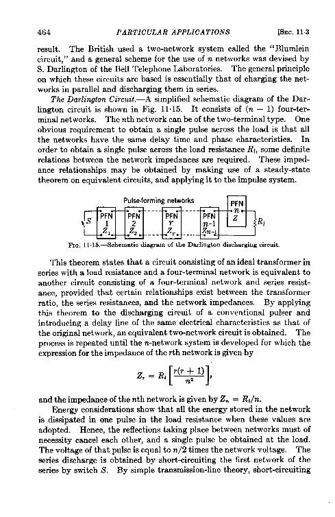
464 PARTICULAR APPLIC’A TIONS [SEC,11.3
result. The British used a two-network system called the “ Blumleincircuit, ” and a general scheme for the use of n networks was devised byS. Darlington of the Bell Telephone Laboratories. The general principleon which these circuits are based is essentially that of charging the net-works in parallel and discharging them in series.
The Darlington Circuit.—A simplified schematic diagram of the Dar-Iington circuit is shown in Fig. 11“15. It consists of (n – 1) four-ter-minal networks. The nth network can be of the two-terminal type. Oneobvious requirement to obtain a single pulse across the load is that allthe networks have the same delay time and phase characteristics. Inorder to obtain a single pulse across the load resistance RI, some definiterelations between the network impedances are required. These imped-ance relationships may be obtained by making use of a steady-statetheorem on equivalent circuits, and applying it to the impulse system.
EMT:E:&RFm. 11. 15.—Schematic diagramof the Darlingtondischargingcircuit.
This theorem states that a circuit consisting of an ideal transformer inseries with a load resistance and a four-terminal network is equivalent toanother circuit consisting of a four-terminal network and series resist-ance, provided that certain relationships exist between the transformerratio, the series resistances, and the network impedances. By applyingthis theorem to the discharging circuit of a conventional pulser andintroducing a delay line of the same electrical characteristics as that ofthe original network, an equivalent two-network circuit is obtained. Theprocess is repeated until the n-network system is developed for which theexpression for the impedance of the rth network is given by
[1T(T+ 1)
Z,=RZ ~)
and the impedance of the nth network is given by Z. = RJn.
Energy considerations show that all the energy stored in the networkis dksipated in one pulse in the load resistance when these values areadopted. Hence, the reflections taking place between networks must ofnecessity cancel each other, and a single pulse be obtained at the load.The voltage of that pulse is equal to n/2 times the network voltage. Theseries discharge is obtained by short-circuiting the first network of theseries by switch S. By simple transmission-line theory, short-circuiting

SEC. 11.3] MULTIPLE-NET WORK pULb9ERS 465
one end of a network is equivalent to reversing the potential of the net-work, thus putting it in series with the second network. The voltage-reversal process is continued until the pulse appears across the load. Itmust be noted that the reversal process results in a fixed time delaybetween the firing of the switch and the appearance of the pulse at theload. The recharging of the network can be accomplished by the samemethods as have been discussed in the case of a conventional line-typepulser.
The Blumle-in Circuit.—If the relations for the network impedanceobtained above are applied to the case where only two networks are used,ZI = R1/2, Zs = R1/2. For two networks, however, the constraining
Network1 Network2
~transformer
w’Magnetron
FrG. 11.16.—Schematic diagram of the Model 16 pulser.
conditions are not as severe as in the general case described above, andmatched conditions are obtained if the sum of the network impedancesis equal to the load impedance, or 21 + Zz = Rz. In this way it ispossible to match a high-impedance load directly to a low-impedancenetwork by the addition of another network.
Some advantages can be derived from using two networks of equalimpedance. For instance, the practical pulser described hereafteruses two networks of equal impedance, which can either be connectedin series as in the Blumlein circuit to obtain a pulse power of 10 Mwfor a pulse duration of 1 psec, or connected in tandem to obtain a pulsepower of 5 Mw for a pulse duration of 2 psec by connecting the switchas indicated in Fig. 11.16. A-c resonant charging was used, and therotary spark gap was mounted on an extension of the generator shaftand provided with phasing control. The networks have impedancesequal to one half the load impedance (magnetron impedance divided by
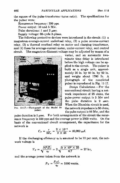
466 PARTICULAR APPLICATIONS [SEC.] ~.3
the square of the pulse-transformer turns ratio). The specifications forthe pulser were:
Recurrence frequency: 350 pps.Power output: 10 and 5 Mw.Pulse durations: 1 and 2 psec.Supply voltage: 60-cycle 3-phase.The following protective devices were introduced in the circuit: (1) a
magnetron-average-current underload relay, (2) a pulse reverse-currentrelay, (3) a thermal overload relay on motor and charging transformer,and (4) fuses for averag-current meter, under-current relay, and controlcircuit. The magnetron-filament voltage may be adjusted by means of a
FIG. 11.17.—Photograph of the Model 16pulser.
variac, and an automatic two-minute time delay is introducedbefore the high voltage can be ap-plied to the circuit. The pulser isbuilt as a single unit, approxi-mately 30 in. by 60 in. by 69 in.and weighs about 1700 lb. Aphotograph of the completedpulser is reproduced in Fig. 11.17.
Design Calculations.-For theconventional circuit having a net-work impedance of 25 ohms, thepulse-power output is 5 Mw andthe pulse duration is 2 usec.When the Blumlein circuit is used,the network impedance is 50 ohms,the mlse outmt is 10 Mw, and the
pulse duration is 1 psec. For both arrange”ments o~the circuit the recur-rence frequency is 350 pps and the average power is 3500 watts. On thebasis of the conventional circuit arrangement, the capacitance for thenetwork is
CI? = & = 22;1:;=40,000,jlf.
If the discharging efficiency Vdis assumed to be 70 per cent, the net-work voltage is
‘N=E=2$x:ix25”27kv,and the average power taken from the network is
P.= ‘~’ = 5100 watts.Td

SEC.11.3] MULTIPLE-NET WORK P7JLSERS 467
The rms voltage across the transformer secondary for n = 2 and Q = 12 is
;E~- = _mr =
0.707 X 27 X 103 = ~9n volts2.76 1
Q(l–e2’J)
and the rms current in the transformer secondary is
InirCNE#.oa
= 1.1 amp.‘.IM= 2fiTherefore,
E,- X I.-, = 6920 X 1.1 = 7.6 kv-amp,
The average current in the transformer secondary is
~ CNE~=z—
() %= 0.44 CNEN. = 0.378 amp.%$. 2
The charging inductance is given by
LC=~C.w:
= 5.15 henrys.
This value is the total inductance, but allowance must be made for thesource inductance transformed by the square of the turns ratio of thecharging transformer. According to experimental tests, a transformer
TABLE11.3.—TYPICALOPERATINGCHARACTEIUSTICSFOBTHEMODEL16 PULSER
ChargingcurrentGeneratorvolts, VQ 1.67, ma. Pulsevoltage, kv Pulsepower, NIw
Blumleincircuit
150155160165170185187195197
2202402602803003203403txl380
13.615.416.418,219.120,221.422.623.6
3.74.75.46.67.28.292
10.211.2
Conventionalcircuit
185 250 8 2.5190 300 9.9 3.9205 340 10.9 4.8215 375 ’12.0 5.7

468 PARTICULAR APPLICATIONS [SEC.114
leakage inductance of 3.6 henrys is necessary in order to obtain a totalcircuit inductance of 5.15 henrys.
Typical operating characteristics with resistance load for the Blumleinand conventional circuits are given in Table 11.3.
11.4. The Anger Circuit. -In the conventional line-type pulser in usein this country, the pulse-forming network is charged slowly to a potentialV., and then is suddenly discharged through a load whose impedance isvery nearly equal to the characteristic impedance of the pulse-formingnetwork.
The Anger circuit was developed in this country by H. O. Anger,in 1942.2 The British have used the same circuit in some of theirpulse generators. In this circuit
RI A
1
FI~. 11. 18.—The Anger circuit with ahold-off thyratron.
the network is charged to a po-tential VN through a load of im-pedance very nearly equal to thecharacteristic impedance of the net-work, and the pulse appears acrossthe load during the charging of thenet work.
The Anger circuit also differsfrom that of the d-c charging line-type pulser in that it is necessaryeither to discharge the network orto reverse the polarity of the net-work voltage during the interpulseinterval. The net work can be dis-charged by connecting a suitable
resistance across its terminals, corresponding to conventional resistancecharging. The polarity of the network voltage can be reversed by con-necting an inductance across its terminals, and the same possibilities ofresonant, hold-off diode, or linear operation exist as in the conventionalinductance-charging circuit.
The fundamental circuit as originally designed is given in Fig. 11.18.Assume that thyratron !l’hl has been made conducting, so that point IIis at potential – EM. If some time later, thyratron Th2 is made conduct-ing, (Thl nonconducting), it closes a resonant circuit formed by thecapacitance of the pulse-forming network and the inductance L,. Since
the current cannot reverse in the circuit because of the lll~i(iirect.it~l~:~lproperty of the thyratron, a charge is left on the network that is nradyequal in magnitude, but opposite in polarity, to that left on it after thepulse.
1By J. V. Lebacqz.zJ. V. Lebacqz, H. O. Anger,and T. W. Jarmie, “ hlcrhanical VawaIII Swit(IIPS,
TransmissionLineand RC PulsingCircuits,” NDRC 14-156,U. of Calif., Jun(>1, 1943,

SEC. 11.4] THE ANGER CIRCUIT 469
Before thyratron Th, is made conducting a second time, a potentialalmost equal to 2Ew appears across it. At the time of firing, the equiva-lent circuit is that shown in Fig. 11.19. The current flowing through thecircuit when the switch is closed is given by Rl _
v. + EW
n
PFN+
I1=RP+RJ+ Z.’ s,:C,
and the voltage appearing across the load is rp
VZ = I&t =VN + Eu Rl
Rp+Rl+ZN “FIG. 11.19.—Equivalentcir-cuit at the startof the pulse.
Assuming matched conditions (ZN = Rz) and neglecting losses (R, = 0),
After the pulse, the pulse-forming network again has a voltage EM
across it, and the schematic diagram of the potential-reversing circuit isgiven by Fig. 11.20. The pulse-forming network can be represented by
its capacitance C., if the resonant period of
TJ
R, ~P +c~- L. and CN is large compared with the pulseduration.
Then, one half cycle after switch i% is closed,
s~V. = EMe–~,
F1@. ll.20. —Sche-matic diagram of the where Q = wLJRt, and R, is the resistance of thepotential-reversingcir-cuit. potential-reversing inductance and switch Sz in
series.The load voltage for the following pulses can then be written, for
matched conditions and no losses in the switch S1,
vt=Ewl+e-fi2“
For a value of Q of approximately 15,
. 1e–% ~ e–o.l = —1.105
= 0.9,
andVZ ‘= 0.95Ew
In general, VI can be written

470 PARTICULAR APPLICATIONS [SEC.11.4
The peak current taken from the power-supply filter condenser is
——
I, =Ebb(l + e ~Q)
R. + R, + Z.’
and the average current is
The average power output is given by
.
the average power input is.
~~(1 + e 2Q)Pi.v = Et.b . I.,V = R ~ Rl ● ~ rf,,
P
and the pulser-circuit efficiency is given by
—— (1 + e-~Q)
RP+R[+ZNR,.
It can be seen from these relations that the performance of this circuit isessentially the same as that of the conventional line-type pulser.
A modification of this circuit was introduced a little later in order to
R, A
m
= Lc B
= Th,%
---
.
iFm. 11.21.—The revised Anger
circuit.
eliminate the necessity of the thyratron Thz
The value of the inductance L. was increaseduntil the natural period of oscillation of theL.C~-combination was exactly twice the pulserecurrence period. Under these conditionsthe network potential-reversing process oc-cupies the full interval between pulses, cor-responding to normal resonant charging ofthe standard pulser circuit. A circuit diagramis given in Fig. 11.21.
Further investigation also- showed th~t the value of the inductancecould be made larger than that corresponding to resonance. In thiscase, the current in L. never drops to zero, and the potential across thepulse-forming network reverses in a more linear fashion, corresponding tolinear d-c charging of the normal line-type pulser circuit.
Since the Anger circuit gives essentially the same performance as thecircuit discussed in Chap. 9, the reasons for using it mllst depend onpractical considerations. Probably the principal disadvantage is that therectifier-output filter capacitance must be able to withstand the additional

SEC. 11.5] THE NONLINEAR-INDUCTANCE CIRCUIT 471
heat produced by the pulse current flowing through it, and must also belarge enough to prevent an appreciable drop in the pulse voltage. From apractical standpoint, a capacitance ten times the pulse-forming-networkcapacitance should prove ample. In general, it is found that this valueis also required to keep the rectifier ripple within reasonable limits.
The principal advantage of the circuit is apparent in applicationsrequiring high voltages in crowded places. It may be noted that, inthe Anger circuit, the maximum instantaneous voltage to ground at anypoint in the circuit does not exceed the d-c supply voltage, whereas, inthe usual line-type circuit, it is twice the d-c supply voltage.
Little difference in the transformers may be expected, the rectifierfilaments are at ground potential instead of Ew, but the thyratron cathodeis at —EM instead of ground potential, requiring, of course, the additionof an insulated trigger transformer for the thyratron grid.
11.6. The Nonlinear-inductance Circuit.1-This section is concernedwith pulse generators in which nonlinear inductances are used as theswitching elements. These pulsers can produce a high voltage acrossthe load from a low-voltage power supply without the use of a pulsetransformer. By suddenly reducing the current in a linear inductanceto zero, the energy stored in the associated magnetic field is transferredto a capacitance. The resultant high voltage across the condenser causesa large current to build up in a nonlinear inductance, which soon reachescurrent saturation. Upon saturation, the inductance of the nonlinearcoil immediately diminishes to a very small value and, together with thecapacitance, acts as a high-impedance pulse-forming network and deliversthe pulse to the load.
The coil has a toroidal winding on a spirally wound molybdenumpermalloy tape core. The tape has a thickness of about 1 mil and aninitial permeability of at least 10,000. The switching impedance ratioand the time of saturation of the coil are controlled by the proper propor-tioning of both the weight of the core material and the diameter andnumber of turns on the coil. For a typical coil the inductance changesfrom approximately 1.5 h to 100 ph at a pulse recurrence frequency of3600 pps, and the time jitter can be held to less than 0.05 psec.
The nonlinear-inductance pulser operates in the following manner.The tube 2’, (shown in Fig. 11.22), which is normally cut off, is madeconducting by means of a rectangular-wave grid excitation (E~ in Fig.11.23). Plate current from a high-voltage source flows through thelinear inductance L 1, and the tube is allowed to conduct for a timesufficient to permit this plate current to build up to a point nearingcurrent saturation (~L, in Fig. 11.23). This duration is made equal toapproximately 25 per cent of the interval between pulses. At the time
By L. G. Keretaof the Bell TelephoneLaboratoriee.

472 PARTICULAR APPLICATIONS [SEC.115
when the current is built up to the greatest usable amplitude for theexcitation applied, the tube is suddenly cut oil. Peak current amplitudesbetween 0.5 and 3.5 amp are obtained in L,, depending on the outputrequirements. A 5D21 tetrode is very satisfactory as tube T, for apulser output of about 200 kw. During the time the tube conducts, thenonlinear inductance L2 operates in the linear region where its induct-ance is about 1 to 1.5 henrys. At the cutoff instant the energy in theinductance L1 begins to transfer to the capacitance Cl, and current ofthe opposite sign begins to build up in the nonlinear inductance. Thisinductance is designed so that thetime required for the core to saturateis equal to the time for the condenserto become fully charged. At thkinstant the condenser suddenly dis-charges and energizes the magnetron(Z~L in Fig. 11.23). The pulse ap-plied to the magnetron from thepulse-shaping elements has a trape-zoidal shape (EMAGin Fig. 11“23);
.FIG. 1122.-Basic circuit for a
nonlinear-inductance pulser. (courte8~of the Bell Telephone Laboratories. )
I
10# sac+
A
I(ti~;i:J~g c1
charges)
=5-
0.3ESCFt~.11.23.—Typical wave shapes in a
nonlinear-inductance pulser. (Courtesy ofthe BeU Z’elepbne Laboratories. )
the voltage pulse has a base about 1 psec long and a flat top of about0.3 ~sec duration. For the operating conditions shown in Fig. 11.23, thethreshold voltage for the magnetron is about 11 kv. Therefore, it isapparent that both the current pulse and r-f pulse have a base timeduration equal to the duration of the voltage pulse at the thresholdvalue (EMAGand lM.G in Fig. 11“23). The resultant r-f pulse has abase about 0.5 psec long and a top 0.3 ~sec long.
It may be noted, from Fig. 1124, that the nonlinear inductance isoperated with a d-c bias, For circuit simplicity an external bias sourceis shown here, and circuit arrangements that require no external biassource are described later. With the application of bias, the cycle of

SEC.11.5] THE NONLINEAR-INDUCTANCE CIRCU1 T 473
operation is started with the nonlinear inductance in saturation, asshown on the B-H characteristic of Fig. 11’25 at point 1~. When thetube T1 starts to conduct, current flows through the tube from twosources: (1) the linear inductance L1, and (2) Cz and the nonlinearinductance ‘Lz. Current flows fromthe full voltage of the high-voltagepower supply (1200 volts) duringthe cutoff period. This current isin a direction opposite to the biascurrent and causes the nonlinearinductance to move its operatingpoint to the linear range as shownby the arrow indicating a rising B.
The bias current is adjusted tolimit the ma~mum B to a valuejust below the saturation pointshown on the positive side of thecharacteristic.
source (2) “because Cz has assumed
L, L,
.FIQ.11.24.—Nonlinear-inductancepulser
with externalbias. (Courkxu.f the BellTefephone Laboratories.)
The pulse-shaping circuit (Fig. 11.26) was evolved from the attemptto use an equivalent of the Guillemin circuit, a pulse-shaping circuitthat can be represented by sections of series-tuned circuits in parallel.The variation attempted here was an equivalent circuit that used thenonlinear inductance and capacitance in series for the first section, andintroduced shunt-tuned circuits in series with the above combination.
This
IB+
o
Fxa. 11 .25. —Hysteresisloop of a nonlinear inductance.(Courtesy of the Bell TehephoneLaboratories.)
L5 G ~
E
G c,, 4 c,
.FIG.11 .26.—Pulse-forming
network for 8 nonlinear-in-ductance pulser. (Courte.V oftlu Bell Telephone Labora-tories.)
much to be desired because ofattempt to square the pulse leftparasitic effects introduced by component proximities. In its final form,which was determined experimentally, the first element in the networkconsisted of a nonlinear inductance and its shunt capacitance in serieswith C,. The inductance Ls was adjusted to tune to a higher harmonicof the pulse recurrence frequency with the tube capacitance Cr, and LO

474 PARTICULAR APPLICATIONS [SEC.11.5
was adjusted similarly to tune with the capacitance of the diode andmagnetron. The resultant circuit is effectively a three-terminal networkin which Cl, CT, and CN=are charged to the full circuit voltage. Uponsaturation of Lz, the condenser CNLdischarges through Lz and definesthe slope of the pulse voltage up to the threshold value of the mag-net ron. The voltage from threshold is maintained by the energy inC,, and declines at a rate that depends on the product of the higherorder elements in the network. The final pulse shape resulted from acompromise between the desire for a rectangular pulse and that forsimplicity in the network.
Dependent on the application, three basic transmitter circuits havebeen used. The first, see Fig. 11.22, is described with the operation of
FIQ.-L.
11.27.—Diagram showing a method to supply the bias for the nonlinearfrom an RC-circuit. (Cowtesvof the Bell Telephone Labordories.)
inductance
the basic circuit, anduses anexternal source of bias supply. The othertwo circuits use no external power for the supply of bias, and, as a con-sequence, they have been more widely used in practical applications.The first of these, shown in Fig. 11.27, iscalled thedynamic-bias circuit.It employs the combination R,CZ to provide the bias. The values areso chosen that the charge which accumulates on CZ during the cutofftime and is dissipated during the period of tube conduction does notsaturate the nonlinear inductance. Also, Cj must beso large comparedwith Cl that appreciable energy is not lost during the discharging period.Likewise, RI must be large enough to limit the tube current through thenonlinear inductance to a value that is less than the saturation value.During the discharge, the value of CZR1 must be such that the currentin the nonlinear inductance builds up to the saturation value in a timeequal to the charging time of Cl. It is found possible to meet theserequirements with relatively noncritical values of C and R. The secondinternal-bias circuit shown in Fig. 11.28 is called the multifilar-biascircuit. The hiasin~ circuit is very similar to that shown in Fig. 11.22,

SEC.11.5] THE NONLINEAR-INDUCTANCE CIRCUIT 475
the difference being that the average plate current of the tube T1 suppliesthe bias for the nordinear inductance. Since the plate current is pre-determined by the operating conditions, the proper biasing point isobtained by adjusting the number of turns on the nonlinear inductanceuntil the proper number of ampere-turns of bias is obtained. Sincethis number of turns is greater than the optimum number for the dis-charge, the additional turns are ob-tained by winding them in multi fllarfaehion with the windinE value that *“h
Ix!uf-.
is optimum for the discharging cir- ~\
cuit. As a result, the nonlinear in-ductance has between two and four L2 , Lfilar windings, depending on thepower-output requirement. Sincethe proper bias polarity is opposite c, + HV
in direction to the normal datecur- =rent flow, the current must be sup-
FIG. 11.2S.—Diagram showing theelimination of external bias by multiiilar
plied through a linear inductance in windings in the inductances. (Cowtav
order to allow current reversal in theof theBsll TslePhime Labordor&)
nonlinear inductance. The linear inductance is aiso proportioned bymultifdar means in order to allow a division of inductance between theelements of the nordinear inductance. An auxiliary consideration is: thatthe voltage across the nonlinear and choke coils be kept at a fimum;this is also accomplished by the multifilar windings.
Fm. 11.29.—Photo~aphs of nonlinear:inductance coils. (Courte8U of the Bell TelephoneLabOratoriw.)
A photograph of the nonlinear inductance used in the circuit of Fig.11“27 is reproduced in Fig. 11“29a, and three stages in the constructionof a multiflar-winding coil for the circuit of Fig. 1~.28 are shown in~g. 11.29b. The core for the coil shown in Fig. 11.29a weighs about 400grams, and the finished unit weighs about 1.5 lb for a pulser having apulse-power output of about 200 kw. Photographs of the assembly

476 PARTICULAR APPLICATIONS [SEC. 116
of the pulser components for the circuit of Fig. 11”27 are reproduced inFig. l130a and b. The completed assembly is enclosed by an oiltightbox, and contains all of the components shown in the diagram with theexception of the tubes and the resistor R 1.
In pulse generators using a nonlinear inductance as the switchingelement, it is possible to obtain small time jitter, and to operate con-tinuously at high pulse recurrence frequencies (greater than 4000 pps)if necessary. The pulser operates also at pulse durations longer thanthose mentioned above, but for durations greater than 1 ~sec the effi-ciency becomes poor compared with that of conventional line-type andhard-tube pulsers.
(b)
FIG.11.30.—Photographs of the component assembly for the nonlinear-inductance pulscrcu’cuit of Fig. 11.27. (C’ourtesv of the Bell Telephone Laboratories.)
11.6. Special-purpose Output Circuits.’ Halj-wave Single-phase
Charging.—The a-c resonant pulsers described previously in this chapterhave full-wave, or single-cycle, charging circuits. In these circuits asimple switch that is synchronized with the supply frequency and madeconducting in proper phase relation with the charging voltage serves todeliver a unidirectional pulse to the load, and the pulse recurrencefrequency is, in general, equal to the supply frequency.
For half-wave charging, discussed in Chap. 9, the pulse recurrencefrequency is twice the supply frequency, but the charge on the net~rork isof opposite polarity on alternate pulses. Accordingly, a conventionaldkcharging circuit would lead to output pulses of alternating polarity.Two special switching arrangements have been used in order to obtain aseries of unidirectional pulses across the load by rectifying action.
The first of these is shown in Fig. 11.31, in which the rotary gap G
1By R. S. Stanton.

SEC. 116] SPECIAL-PURPOSE OUTPUT CIRCUITS 477
is of a special design that provides the rectifying element in the circuitas follows. When the network voltage assumes a maximum value withterminal a positive and b negative, the switch assumes the positionshown in the figure; a is therefore connected to ground, and a negativevoltage appears at the terminal c of the load. One half cycle later, thepolarity on the network is reversed, the switch connects b to ground anda to the load at c, and again a negative pulse appears across the load.
One pulser based on the circuit described above was required to deliverSpsec pulses to a load impedance of 450 ohms at a maximum pulse powerof 1.8 Mw. The pulse recurrence frequency was 120 pps, and the a-csupply was a 115-volt 60-cycle single-phase line. The rotary-gapswitch was driven by an 1800-rpm synchronous motor with electricalmeans for automatically selecting the phase required to deliver a negative
~----- ----------------- ~\\\‘\
$3
FIG. 11.31 .—Pulser using a-c resonant half-wave charging.
pulse. A special transformer was designed to provide the correctinductance for resonant charging.
Design Calculations.—The requirements for the pulser are:Pulse power P,: 1.8 Mw.Pulse duration r: 5 psec.Pulse voltage Vl: 28.5 kv.Load impedance Z1: 450 ohms.Average power: 1080 watts.Pulse recurrence frequency j, = 120 pps.
Assuming a pulse-forming-network impedance of 50 ohms to matchthe pulse-cable impedance, the following values are obtained:
Pulse-forming-network capacitance C. = 0.05 ~f.
J 3Pulse-transformer stepup ratio ~ = 1.
NDischarging efficiency m = 70 per cent (assumed). Using the above
values, the network voltage is given by

478 PA RTICL-I,A R APPLICA l’IONS [SEC.116
:md the power to be taken from the network is
P.v = 1% = --1.8 X 106 X 5 X 10-6 X 120 ~ ~580JYatt\
i7.,
11<1
‘1’he transformer-secondary voltage is
with n = 1 (half-cycle charging) and Q = 12,
0,707 X 23 X 103 ~ ~1 ~vI?,,z,n”= -- – ~.47 ,
anfl the transformer-secondary cllwwlt is
Imrc’., ),,,@,, _7r X5 X10-S Xll XIOJX @(2r)60
‘,1!,. ‘ 246 – 2 X 2,45= 0.19 amp.
Tljerefore,E,rmq X I.,,m == 2100 volt-amp.
The charging inductance is
1‘c = C% = (5 X 10⁻⁸)(27 X 60)’ = 138 ‘enrys’
This value was used in dmigning the a-c resonant transformer becausethe source inductance could be ncglcctcd.
2’//{; Thvrairon Bridge.—A thyratrun bridge can be used instead of therotary gap to obtain p\Ilscs of identical polarity, as indicated in Fig. 11.32.
When terminal a of the pulse-forming network has reached its maxi-mum positive charge, a trigger pulse is supplied to Vl”la causing it toconduct. Its plate is thus brought very nearly to ground potential,and a negative impulse is applied to the cathode of V!l’lb through thecapacit:mce of the pulse-forming network. Because of interelectrodecapacitance, the grid does not become negative as rapidly as does thecathocie. Thus, VTlb is also made conducting, and the dischargingcircnlit is completed through Rl, V!flb, the pulse-forming network,and VZ’la. At the peak of the next charging cycle (the sllcceedinghalf-cycle of supply voltage), VT2a and VT2b are made to conductin a similar manner. Th~ls, the thyratron bridge serves the same pur-pose as the rectifying rotary gap s~ritch.
Assuming perfect voltage division across the bridge, the networkvoltage may be twice the voltage rating for a single tube and, since each

SEC.11.6] SPECIAL-PURPOSE OUTPUT CIRCUITS 479
pair of tubes conducts at only half of the output pulse recurrence fre-quency, the duty ratio may be twice that for a single tube. The pulsecurrent is limited to the current rating of a single tube, so the maximumaverage power output may be four times that for a single thyratronswitch.
A special trigger-pulse generator is required for use with the thyratron-bridge circuit, It must supply alternate trigger pulses to Vl”la andVT2a spaced exactly 180° in the supply cycle, and phased with respectto the charging voltage so that each tube is caused to conduct when thenetwork voltage reaches a maximum.
An experimental pulser was constructed and tested at the RadiationLaboratory using 4C35 thyratrons and a 400-cycle a-c supply. The
.,,
&F1~.11.32.—Schematic diagram of the thryratron-bridge circuit.
pulse recurrence frequency was therefore 800 pps. The 4C35 thyratronshave maximum pulse ratings of 8 kv and 90 amp, but, since the two tubesare in series, the maximum allowable network voltage is 16 kv. Assum-ing matched load, the value of Z~ that causes the pulse current to fallwithin the maximum rating is
The network and load impedances were chosen as 100 ohms each, theload being a noninductive resistance. For a pulse duration of 0.9 psec,the pulse-forming network had a measured capacitance of 4550 p~j.
The charging-transformer characteristics were as follows:Transformer-secondary voltage,
..
E~- = z= 7.7 kv.
——Q(I – e ~)
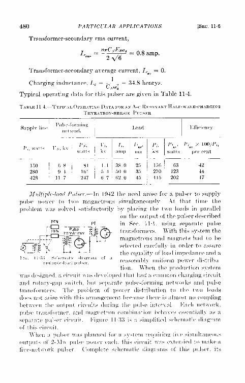
480 PA RI’IC1”LAIZ APPLICATIONS [SEC. 116
Transformer-secondary rms current,
In~C.yEW.- — = 0.8 amp.‘rm,
= 26
Transformer-secondary average current, l,~v = 0.
~harging in(lllctance, L. = ~ !7 = 34.8 henrys..
Typical opemting tl:~ta for this p’;Ilser are given in ‘~ahlc 11.4.
TABI.E 114.-rI’YI,IC.\I. OI,I;R.\TI>G1).\r.\ roR AX .{-c RE<ox.%x~ ll. +ll--\V.*Vfi:-{H \RG1XG‘[ ’IIYR.+~R(lX-BR1 l)(:E l>ll.sER
1’,, \Yatt,1’,, I,> Ilav. ~ Plnv, I’lav x 100/1’,,
1“.y,li\ ,:;;:;5 P,,k, al]lp I 111:1 : k\v IV:ltts pcr rrnt
l.-
1,50 ~ 68 I 84 4.1 3S 0251 136’ 63 42
280 91 l(il i 5.4 ,-)0 o 35 270 123 44
428 117 247 (i.7 (i2 o ~ 45 415 2(Y2 47
.lfl~lt~pl~-lend F’((1.scr,—In 1{)42 the ncml arose for z pnlscr to NIPPIJJpIIlsr polier to t\\t) In:lgnetr(ms sinllllt:i]lcollsly. .\t th:lt time theprol)lcm J\-:wSOIJC(Is:itist’tict,orily hy p]acing the tlro loa(ls in parallel
on tl]e o\Itpllt, of the plllscr descrilxdPFN in S(T. 11.1, [Ising sep:lrate plllse
- t~:$$:., iPFN tr:lnsformrrs. lVith this systrm the
.. . . . . -- m:lg]~etrx)ns nn(l nmgnets l!:l(i to he
~1~[~ ~pBd selecte(i c:~refllllv in or(lcr to assl[re
tile (’(l(l:llity of 10:1(1inlp(’(l:lnw :ln(l a1I,;. I1:+1 ~,,]l,,lll:ltll,<11:1~1’:1111of :1
,),,111,,)l(,.lO,,(1 ,,,,1.,,,. re:uwnal)ly Ilnifornl p(Ilv(’r (list til)ll-tioll. \\”tl(,n t}le I)ro(lll(,tio]l” sjst(,ni
IV:ls (Iesigne(l. a cir(,llit 11”:1s(Ielelt)l)e(l tll:lt ll:L(l :1 (ItIIIIIIlt)n (,ll:ll,~illg (it(,~lit
an(l rot:ily-~:lp s!t il (’11, I)llt sep:lrwte Illlls(’-follllitlg Ilet lt otks :Lll(l ]) IIlsc
tmnsformers. ‘[’he prol)l(’m of poiJ (’r (Iihtril)lltion to i 11(’ t Ii”() 10:1(1s
(10(,s not :11’lse Ivlttl tills :Lll:lllg(’111(’tlt l)e(,:l IIv tll(~t,(>is :Illllost II() (,olll)ling
I)etit-((ll tile olltl)llt (ir((lits (Illring tile I)LIlse illt(r]:ll. I?:L(II n(lllork.
plllw tr’,ln>fol”m(’r. :In(l nl:ignettoll ct)llll)i]l:lt ion lNJll:l\o~ (,sw,llti:llly :1s :L
s(,p:lt:tt[, lJIIIX(Jr (ir(,llit. I;igllte I 1 t;:] is o .sinll)li{itxl s(ll(,nulti( (li:l~mnl
of tliis cil[(lit.
IYII(II ;1 I)llls(,l’ 1!:1s l)l:lllllml for :L ,~y>t(nl ,e(l,li,il]g fif-( sil,]l,lt:,,,(ol,sI this (ir(,llit \\:ls ext(’11(1(1(1to In:lk(’ :L(Illt[)llts of 2-n\\ plllw polv(, r (’:L(, 1
fi\’C-Il(, t\\ ’ol’k pUk,I’ (’omplcte schcrn~tic (li:i~r:lms 01 this I)IIlsrr. its

Fmm
??
12
N
---F
To remote-controlpanel indicator
IJ\y
=9
‘;.
QL=0F(3
I 1 1 1 I 1- I 1- I 1 I II III r
.-
!I’(
—
Jr
Motor~~ Rotarysparkgap
FIG.11.34.—Completeschematicdiagramof themultiple-loadpulseranditscontrolcircuit.
1A
,. ... .,,.

482 PARTICULAR APPLICATIONS [SEC.11.6
control circuits, and its remote-control panel are shown in Figs. 11.34and 11.35.
One of the principal problems associated with this pulser was thedesign of arotary spark gap that could handle the high current (1070amp) without excessive electrode wear. A switch that would operate for
[-~ .+IId “
+
I
3 -*Input
Recycle~ S8Safety
-. ==_ = --I 2
Bus~
gay-q\sl
BusIIP ~1---
RIw Time meter
Thermal
~
s
--,, A===:
--------- ----..—- —- —-- —---- ---------Terminalboard1 Terminalboard2 Terminalboard3
FIG.11.35.—ComPleteschematicdiagramof theremote-controlpanelfor themultiple-loadpulser.
at least 1000 hours without the replacement of electrodes was finallydeveloped.
Electrical Design.-The specific requirements for this pulser were asfollows :
Pulse power, PI: five outputs of 2 Mw each.Pulse duration, ~: 1 ysec..4verage power, P1,V: 3500 watts (total).

SEC. 116] SPECIAL-PURPOSE OUTPUT CIRCUITS 483
Pulse recurrence frequency, j,: 350 pps.Load impedance, Z1: 450 ohms.Pulse-forming-net work impedance, Z.: 50 ohms.Total network capacitance, C~: 0.05 X 10–’ farads.Pulse-transformer stepup ratio: ~~ = 3/1.
If the discharging efficiency, Vd,is assumed to be 70 per cent, the networkvoltage ia
and the average power taken from each network is
pH _ ‘~fr – 2 x 10’ xo~-’ X 350 = 1000 watts.~d
The rma voltage across the transformer secondary for n = 2 and Q = 12 is
E~m =%= 0.707 X 24 X 103 ~ ~ z kv
Q(l – e ~)2.76 9
and the rms current in the transformer secondary is
InrC~Ewa
%m “ Z@. 1.28(0.05 X 10⁻⁶)(6.2 X 10³) ~~ (27r X 350) = 1.2 amp.
Therefore,E~m x I,- = 6.2 X 103 X 1.2 = 7.6 kv-amp.
The average current in the transformer secondary is
I~ C.EW.
C.* 2 ()%= 0.44 CNEWO
= 0.44(0.05 X 10⁻⁶)(6.2 X 10³) ~~ (2T X 350) = 0.42 amp.
The charging inductance is
1““G:’ (0.05 x 10-;(% x 350)’ = 4“14 ‘envs ‘tOtal)”
(Only 2.85 henrys of this total value were designed with the a-c resonanttransformer; the remainder was provided by the equivalent inductanceof the source. )
Typical performance data for this multiple-load pulser are given inTable 11.5, and photographs of the equipment are reproduced in Figures11.36 and 11.37.

484 PARTICULAR APPLICATIONS [SEC. 11 cl
-- .-—-----.——.. .- . .-. =
(a) (b)FIG. 11,36.—(a) Nlotor-generator and rotary-gap switch for the multiple-]oad pulser.
(b) Rotary spark gap.
TABLE 115.-TYPICAL PERFORMANCED.*T.\FOR.4 MULTIPLE-LOADPULSER
Generator output ~Pulse-forming networks’ Efficiency
Test I—
No.f,) PPS ~Q :P\-
10, amp P,, kw ~N, kv~ x 100,
ZPN, kw tvolts
per cent
1 356 158 23.1 3.27 18 8 3.11 952 355 179 27 4 4,27 22.0 4.22 983 354 198 28.0 5.10 23,1 4.61 91
Testso.
123
}Iagnetron No. 1 I Magnetron No. 2 I Nagnetmn S0. 3
J7,, ] 1, , Pa”,
kv ma: watts
28 0 14.1 395
z
IPl, VI, Iiav, ‘ P,av, I P,, v,, Il.”,~Plav!kfw kv ma watts lfw kv ma watts
1,15 28.0 13 5 378 , 1.08 27.4 14.7 4031.50 29.0 16.9 490 1,41 28 2 18.5 5221,73 30.0 18.8 564 1.63 29.2 20,81 607
P,,Mw
1.151 49
1,73
IMagnetron N’o. 4
I}Iagnetron 3’0.5
! IEfficiency irr
per cent
TestNo.
v,, I{.v) PI.”! P,, v,, \Il.. ~% P,, ~pav, $x +xkv ma watts Mw kv ma watts 31W kw - ~’m ‘
— . — — —. . . . .
1 \27.9 13.5 377 1.09~27 4! 14.6 400
-228”9~ 117”2 1“4!Y8”5 i 53: i;; ‘~ : i ‘i3 29.8 19.3; 576 , 1.6729.21 20.71 605

SEC. 11.7] MULTIPLE-PULSE LINE-TYPE PULSERS 485
1107. Multiple-pulse Line-type Pulsers.l—The problem of obtaininga rapid succession of pulses from a line-type pulser is complicated by thefact that ail gaseous-discharge tubes known to date have a deionizationtime that is too long to enable the network to become recharged if thepulse interval is to be less than approximate y 100 psec. Hence, in orderto obtain multiple pulses from a line-type pulser, it is necessary to useartifices.
The following three methods have been tried, one of which is used inpractice: (1) a m(dtiple-switch multiple-network circuit, (2) a multiple-#witch single-network circuit, and (3) a single-switch multiple-network
FIG. 11,37.—Cabinet for tbe multiple-load pulser. (a) Side view. (b) Rear view.
circuit. The three methods are discussed separately, and their possibleuses and respective advantages are compared.
llultiple-w”tch Multiple-network Circuit.—The schematic diagramgiven in Fig. 11.38 applies where a double-pulse output is required.As can be seen, this circuit is simply a combination of two identicalline-type pulsers connected to the same load. When thyratron 7%1 isfired, the network PFNI discharges through the load resistance Rt, givingthe first pulse of the series. When Z’hz is fired, the second pulse isproduced in the load by the discharge of PFN,. More circuits cansimilarly be fired in succession to produce so-called “codes” of three ormore pulses. Additional stray capacitance, which may affect the pulseshape, occurs across the load when all the pulse-forming networks areconnected to the load, or to the primary of the pulse transformer. Also,
1By J. V. Lcbacqz.

486 PARTICULAR APPLICATIONS [SEC.11.7
the plates of all the thyratrons are coupled together through the pulse-forming networks. Hence, all output pulse voltages appear, essentially,at the plates of the untriggered tubes. As long as the pulse voltage is
B+I
*
FIG, 11.38.—Circuit diagram for a multipleswitch multiple-network circuit.
negative, no trouble can result.If, however, post-pulse oscillationsappear because of the nature of theload or the pulse transformer, diffi-culties may arise either from exceed-ing the peak forward voltage of thethyratrons that have not yet beenfired, or from the incomplete deioni-zation of the thyratrons that havealready been fired.
The spacing between successivepulses of the same code can beobtained in many ways. A practi-cal method is to use a delay circuit
that is energized when one thyratron is fired and produces the triggerfor the successive pulse. A low-power coded pulser was built on thism-inciple, whose schematic diagram is shown in Fig. 11“39. A brief. . .summary of the design considerations follows.
1.
I ‘i I
RbPFNj
T
1 , , !+
FIG. 11.39.—Basic circuit diagram for a pulser producing a three-pulse code.
When thyratron Z’hl is fired, the first pulse of the code is sent to theload, and, at the same time, the grid of the first half of T, is driven wellbeyond cutoff. When the grid potential again rises to allow the tube to

SEC.11.7] MULTIPLE-PULSE LINE-TYPE PULSERS 487
conduct, the sudden increase in plate current causes a positive trigger toappear on the grid of the second half of Ti, starting the regenerativepulser action and applying a trigger to the grid of Thz. The operation isthen repeated to trigger Th~. The spacing between pulses can easily becontrolled by adjusting the cathode bias of the triodes T~ and Ts.
Resistance charging of the pulse-forming network was chosen becausethis particular pulser was required to operate at random recurrencefrequencies from O to 2000 pps. Resistance charging presents somespecial design problems that are discussed here.
When the thyratron is fired, and until it is completely deionised,the charging element short-circuits the power supply. Hence, a currentEM/R. flows through the tube after the pulse-forming network is dis-charged. If this current becomes too large, the thyratron does notdeionize properly. Even before it stops completely, the deionizationbecomes erratic and may occasionally take as long as 500 gsec, resultingin improper charging for the next cycle.
In order to prevent large variations in pulse power when the recurrencefrequency is changed, it is necessary that the pulse-forming network becharged nearly to the power-supply voltage at the time of triggering whenthe highest recurrence frequency is used.
If T, is the recurrence period, and Tk is the deionizing time corre-sponding to the chosen value of R., the network voltage at the time offiring is given by
Tr – Tb
l’~ = EM(1 – e- RECN),
where CN is the network capacitance. Thus,
T, -T&–a=Eu–VMe
EW ‘
and
c. = T, – Tk
EU “
“In EM – VN
If a variation of X per cent in the network voltage is allowed, VN is
within (1 — X/100) of EM, and the pulse output power does not vary bymore than 2X per cent; the maximum network capacitance is then given by

488 PARTICULAR APPLIC!A TIuNS [SEC. 11.7
Under these conditions, the maximum energy per pulse in the load is
As has previously been shown, R. depends on the maximum currentthat the switch tube can pass and still deionize satisfactorily. If 1,is the value of this current, R, = E&/l~, and
#
Thus, from a design standpoint, the maximum energy per pulse that.can be obtained is proportional to the supply voltage and to the minimumcharging time ( T,~i~ — TJ of the pulse-forming network.
Double-switch Single-network C’ircuit.-’The schematic diagram of thiscircuit is given in Fig. 11“40. Assume that the pulse transformer is an
R,ideal transformer of turns ratio 1/1/1 andthat RI = Z. (matched conditions). Assume
2 also that the filter condenser is charged to a
= potential EM and that the pulse-forming net-+ 4 work is completely discharged. If losses are
. neglected, the pulse-forming network becomescharged to a potential VN = Ew when thethyratron T//, is triggered. Because of the
.C, ~‘m, properties of pulse-forming networks, a pulse2
of voltage E~/2 appears across 1/[ during thecharging of the network. During the pulseboth the plate and the cathode of thyratron
l:l~. 1141)-Circuit di:l- Tl,, are driven negative to – E,,, the plate bygr:~m for a duut>lc-switcl~ the addition of the voltage at point 4 and th~tsingle-uct work pulser.
induced in the transformer winding 5+. Atthe end of the pulse, however, a voltage equal to EN suddenly appearsfrom anode to cathode of Tht, and, to keep this tube from firing, it isnecessary to prevent the grid from becoming more than a few volts posi-tive with respect to the cathode. The use of negative grid bias and theaddition of capacitance between grid and cathode easily accomplishesthis result.
Until thyratron Th2 is triggered both the filter condenser and thenetwork are charged to a voltage Em. When Th2 is triggered, the pulseforming network discharges through winding 5–6 of the pulse transformer,and a puke of amplitude E6~/2 again appears across R,.
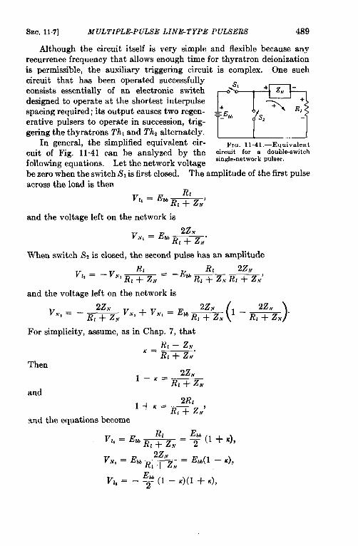
SEC.11.7] MULTIPLE-PULSE LINE-TYPE PULSERS 489
Although the circuit itself is very simple and flexible because anyrecurrence frequency that allows enough time for thyratron deionizationis permissible, the auxiliary triggering circuit is complex. One suchcircuit that has been operated successfullyconsists essentially of an electronic switchdesigned to operate at the shortest interpulsespacing required; its output causes two regen-erative pulsers to operate in succession, trig-gering the thyratrons Thl and Thz alternately.
In general, the simplified equivalent cir-cuit of Fig. 11.41 can be analyzed by thefollowing equations. Let the network voltage
FIG. 11.41.—Equivalentcircuit for a double-switchsingle-network pulser.
be zero when the switch S, is first closed. The amplitude of the first pulse
acrosa the load is then
Vl, = EM ~, ~ ~MJ
and the voltage left on the network is
2ZNVN, = EM ~~-
When switch S2 is closed, the second pulse has an amplitude
RI R, 2ZN‘1’ = ‘v”’ Rt + z.
= –Eu —Rl + z. Rt + zN’
and the voltage left on the network is
v., = – Rly”zN ( 2ZN
)
2.ZN _ .V~, +V~, =Ew R1+z~ l– R, + ZN
For simplicity, assume, as in Chap. 7, that
Rl – z..
‘= R[+Z.Then
l–K=22”
R, + ZNand
2R1l+K=—
R1 + Z.’and the equations become
= EM(1 – K),VN, = EM &2~’~
V,, = – ~ (1 – K)(I + K),

490 PA RTICLrLAR APPLICATIONS [SEC.11.7
and1’.v, = &K(l – K).
The third voltage pulse is
I+ K=_ EbbVI, = (EM – v..,) ~ ~[ I – K(l – K)](I + K),
and the voltage left on the network after the third pulse is
V,, = (Ew – V,”,)(1 – K) + VN,,or
V.y, = E,, (1 – E)(1 + K’).
The fourth pulse is given by
1+.V2, = – v.V3 ~ = – %(1 – K)(l + K)(l + K’),
and the voltage left on the network after the fourth pulse is
v,, = – v’,, ~12&+ V,v, = -%aK(l – K)(1 + K’).
In general, for any pulse,VN(*”.,, (1 + K)Vl(,n) = – ~
Vi,,”+,) = ‘w ‘2 VM(’”)(1 + K),
V,v,,m, = KVN,, m_,,,
andv, ,,m+,,= (1 – .)m% + KVN{,n,.
These values can now be rewritten in the form of series as follows:
Vl(,”) = – z“(1+K)(l – K)(1 + K’ + K’ + . “ “ + K2n-2).
Emv,,,. +,, = ~ (1 + K)[l – K(1 – K)(1 + K2+ K4+ “ “ “ + K’”-z)].
V.,,., = E,,K(l– K)(1+ K’+ K’+ . . . + K“’-z).VN[?”+,)= ~M(l – K)(I+ K2+ K4+ . . . + K’”-’).
Since K is smaller than one, the series are all convergent and the equationscan be rewritten
Vkzm)= – *(l+ K)~=–*(l– K’”),
VII,.+,)=~(l+K)( )1 – K;--+:; = :! (1 + K2”+1),
1 – pVM(,.) = E.K p
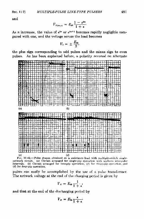
SEC.117] MULTIPLE-PULSE LINE-TYPE PULSERS 491
and
VN(,.+,)1 – K2m
= EW ~.
As n increases, the value of K2” or K’*+l becomes rapidly negligible com-pared with one, and the voltage across the load becomes
~1 = * EM,2
the plus sign corresponding to odd pulses and the minus sign to evenpulses. As has been explained before, a polarity reversal on alternate
(c) (d)FIG.11.42.—Pulseshapesobtainedon a resistimcc lend with lllllltil,l{.-s\vit c.l1 singh.-
network circuit. (a) Circuit arranged for single-pip opcvatiou with ,L,,if,>r,,, i,,te, ,,UIWintervals. (b) Circuit arranged for two-pip opcr:,tion, (c) [or thrm.-,,il, (,l,,r:,t i,,,,. :,,!,1(d) for four-pip operation.
pulses can easily be accomplished by the ust~ of N p(ilw tr:~nsftnmwr.The net work voltage at the end of the ch:trging period is given I)y
V, = EM &-K,
and that at the end of the discharging period by

492 PARTICULAR APPLICATIONS [SEC. 117
The applications of this circuit are not limited to obtaining codedpulses from line-type pulsers. Although it is equally well suited for theconstant recurrence frequencies that are common in radar systems, itsadvantages become particularly impressive when the pulser is requiredto trigger at random intervals. As was pointed out before, the principaldisadvantages are due to the complicated auxiliary circuits required fortriggering the two tubes alternately, and to the precautions necessary toprevent the tubes from going into continuous conduction. It is belie~-ed,however, that where irregularly spaced high-power pulses are required
Lethese disadvantages are outJveighedby the great flexibility of operationand the high efficiency. Oscillogrmnsof pulse shapes obtained by this
Ebb
IImethod are shown in Fig. 11.42. Fig-ure 1142a was taken for a singlepulse in order to show the slight [iif-
& ference in pulse shape that results, inFlu. 11.43. —Circuit diagram for single- practice, from the charging or dis-
switch n]tdtiple-network pulser.charging of the network.
Single-switch Multiple-network Circuit.—The following circuit hasbeen tried and found very successful in obtaining t~~overy closely spacedpulses from a line-type pulser. The principle of operation is identicalwith that of a regular line-type pulser, but an open-ended delay line isconnected in parallel with the load, as indicated in Fig. 11“43. Assumethat 6*, the delay time of PFNZ, is greater than 6,, the delay time of PFX,.When the thyratron is fired, a pulse appears across the load and the delayline. This pulse travels down the line and is reflected at the open end.After a time equal to 262, the reflected pulse appears at the load and givesa second signal.
Simple considerations indicate the conditions under which the twwpulses have the same amplitude. The voltage amplitude of the tirstpulse is given by
R,Z>,,
Vl, = VN,R, + Z.,, ,
Z,,,, +RIZN,
RI + Z>,,and that of the second pulse is
wherea = e~l,
a is the attenuation factor, and 1 is the length of the delay line. The two

SEC. 11.7; Ai~’LTIPLE-PULSE LINE-TYPE PULSERS 493
pulses ‘&at appear across the load have equal amplitude when
~+ R1–z.\7, _lR1+ZN, –7
orZ,., = Rl(2a – 1).
To obtain matched conditions for the discharge of the, pulse-formingnetwork, PFN1, the additional condition
z., =RIZN, = Rt 2a – 1
Rl + zN, a
must be satisfied.Some limitations of the system become obvious immediately. If
2a approaches 1, the values of ZN, and Z~, ammoach zero. The total-.attenuation of the line PFNZ in-creases rapidly with the length ofthe line, or the time delay betweenpulses; hence, a limit on maximumpulse separation is soon reached.Figure 11.44 shows the similaritybetween the two successive pulsesobtained by this method for adelay time of approximately 3psec.
If, however, the time delay in
. .
FIG.11.44. —Oscillogram showing r-f en-velope of pulses obtained wi h the circuit ofFig. 11.43.
PFN2 is made less than ~lalf that in
PFN,, the wave reflected from the end of the delay line appears at theload before the main pulse is ended. If the delay line is open-circuited,the polarity of the reflected voltage is the same as that of the pulsealready appearing across the load, and an increase in pulse amplituderesults. If the delay line is short-circuited, the reflected voltage is ofopposite polarity, and produces a decrease in the amplitude of the mainpulse.
General Comparison.—The multiple-switch multiple-network circuitis the most flexible one that produces multiple pulses; there are almostno limitations on the spacings that can be obtained. The main dis-advantage is the large number of components that are necessary becausea complete pulser circuit is required for each pulse. The double-switchsingle-network circuit is almost as flexible as the multiple-switch multiple-net work circuit, except that the minimum spacing bet ween successivepulses is limited by the deionization time of the particular switch. Thistime can be decreased somewhat by operating the thyratrons at voltagesand currents below the rated values. The main disadvantage of thiscircuit is the complex electronic switching circuit that is necessary topulse the two switches alternately, and the necessity of ha~~inga power

494 PARTICULAR APPLICATIONS [SEC. 11.8
supply voltage that is equal to the network voltage (instead of half this
voltage, as is usually the case for d-c inductance charging). The high-insulation trigger transformers may also cause some difficulty, but someof these disadvantages are outweighed by the absence of any chargingcircuit.
The single-switch multiple-network circuit is the least flexible of thethree. It has been described here because it represents a very simplemethod of obtaining two closely spaced pulses, or pulses of irregular stepshape.
11.8. Multiple-switch Circuit for Voltage Multiplication. ‘—For high-power line-type pulsers having high-impedance networks, the voltageson the networks tend to become high, and may reach values of 50 kv ormore. Such high voltages usually lead to engineering difficulties, andsome form of impulse-voltage multiplication is therefore desirable. The.Marx multidier circuit mav easily be adapted to thk use. The basic
““-=—I~lG. 11.45.—Three stage Marx circuit
adapted to the line-type pulser for multipli-cation of pulse voltage.
circu-it uses the Type A pulse-forming network and is shownin Fig. 11.45 for three-stagemultiplication.
The condensers C comprisethe storage capacitance of theType A network. Since thesecondensers are in series, each onemust have a capacitance of nC.V,
where n is the number of stages and CN is the required capacitancefor the network storage condenser. The voltage multiplication isobtained by charging the condensers in parallel and discharging themin series. In the ideal case, the voltage stepup ratio for an n-stagecircuit is n. In practice, however, about 10 per cent of the voltage isusually lost because of currents flowing through the inductances L.
The pulse discharge is initiated by firing the spark gaps G, which may,of course, be replaced by any other suitable switch. The isolatingchokes L serve to prevent the condensers from being short-circuitedthrough the gaps during the pulse.
It is clear that the isolating chokes L must have inductance that issufficient to prevent an undue portion of the pulse current from beinglost through them. An estimate of the required inductance may bemade by calculating the circulating currents that flow during the dis-charge period. Some loss may also occur because of circulating currentsif the gaps do not fire simultaneously. Under most conditions, however,the time lag in the firing of the gaps is less than the pulse duration T,and the approximate calculation remains valid. Triggered switches
1By H. J. White.

SEC. 11.8] CIRCUIT FOR VOLTAGE MULTIPLICATION 495
such asthyratrons or fixed spark gaps usually have very small time lags.For the purpose of an approximate calculation, it is sufficiently accurateto consider the current flowing through one inductance and one con-denser C in series, thecondenser being initially charged to a voltage ~N.
The current is then
J<sin tiLc = VN
L~m.
The period of the LC-circuit must be large compared with the pulsedurationr, and, onthe basis of this assumption,
J
Ct VNtiLC = VN ~.=y=x.
The maximum value that i LCcould have during the pulse if the condenserwere not otherwise discharged is
(iL.)u,u = $m,
and the pulse current in the load is given by
nvN1’==N”
Eliminating VN between these two equations,found to be
the expression for L is
2.2?N,L= — =.
[J
n iiLc)m.x11
As an example of the order of magnitude of L, let
ZN = 1000 ohms, ~ = 10–g see, (i..)= = ~oln=3, —
11Then
h = 2 x 1000 x 10–63 x 0.01
= 67 mh.
Experimental data on the effect of the isolating-choke inductance onthe current efficiency are given in Fig. 11.46 for a two-stage circuit.Current efficiency is defined as the ratio of n times the average load cur-rent to the input average current, where n is the number of stages, or2(11.,/1,=.). If there were no circulating currents in the isolating chokes,the current efficiency, by Kirchhoff’s law, would be 100 per cent.
Unequal storage-condenser capacitances C also cause circulating cur-rents, which produce losses in the gaps and the condensers as well as in

496 PARTICULAR APPLICATIONS [SEC.11.8
the chokes. The isolating chokes usually have an iron core, and, forhigh-power circuits, they can be mounted conveniently in the tank ofthe pulse-forming network.
A variation of the circuit of Fig. 11“45 that is particularly applicableto the two-stage Marx circuit is shown in Fig. 1147. Here the highest
100
I ~----
FIQ.
SC
20
(I’LLPulse-shaping G
/’ elements1--1
‘ SGwce b LHighhage
k JJ R,
~1 ~z
. .
I
00 20 40 60 80 100Isolatinginductancein mh
11 .46. —Effect of isolating inductance in the Marx circuit on the current
voltage to ground at any instant is equal to the load pulse voltage, andthe problem of insulation is therefore simpler than that imposed bythe original circuit. The rotary spark gap can easily be adapted for useas the switch in a Marx circuit by mounting the rotating electrodes on an
*: ,,source
1 dL
~Pulse.ehaping
elements —
FIG.
1 ,
11.47.—Variation of the Marx circuit to reduce voltagee to ground,
insulating rotor and using one set of fixed electrodes for each gap required.An n-stage Marx circuit would have n sets of fixed electrodes. The gapscome simultaneously into firing position, and very smooth operation isobtained when the switch is well built.

PART III
PULSE TRANSFORMERS


CHAPTER 12
THEORY OF PULSE TRANSFORMERS
BY W. H. BOSTICK
12.1 General Tranaforrner Theory. -Of the devices that have beendeveloped for the transformation of energy and power the electromagnetictransformer, which changes the ratio of voltage and current while main-taining their product constant, has proved one of the most useful. Elec-tromagnetic transformers in general and pulse transformers in particularhave been used—
1.
2.3.4.
5.
It
To transferor control energy by raising a voltage above a thresholdor barrier level.To invert the sign of voltage.To effect “d-c isolation” between source and load.To deliver the correct amount of power to a load of a given resist-ance by changing the voltage to the proper value.To effect maximum transfer of energy (or power) from source toload by a transformation of energy to the proper impedance level.
is ~ossible to conceive of a perfect electromagnetic transformer(see pag~ 504 of Sec. 12”1) which ‘would operate su~cessfully over anyrange of frequency, impedance, and power levels. For various reasons,which are discussed later, such a perfect transformer cannot be built.Any transformer that can be built has certain limitations in its range ofoperation and should be designed to give optimum performance underthe conditions of operation for which it is intended.
Many different types of transformers have been developed to performthe many functions and to cover the various ranges of operation of elec-tromagnetic transformers. For example, there are filament and “power”transformers, which operate steadily on a sinusoidal input at the variousstandard power frequencies and voltages. There are audio transformers,which are designed to operate over the audible range of frequencies, someat high-power levels and others at low-power levels. There are r-ftransformers, which, when used in the circuits for which they are intended,pass only a narrow frequency band of r-f energy.
The development of pulsed radar created a need for a relatively newtype of transformer—a transformer that transforms the energy in a pulse
499

500 ELEMENTARY THEORY OF PULSE TRANSFORMERS [SEC.12.1
having a more or less rectangular shape and a duration of the order ofmagnitude of 1 psea.
In general, such pulse transformers are used to perform any or all ofthe functions listed at the beginning of this chapter. One individualpulse transformer is often used over a fairly wide range of pulse durations,voltages, and impedances.
Pulse transformers are also used extensively (usually at low power)in one type of puls~generating circuit, the regenerative pulse generatoror blocking oscillator, in which energy is introduced from the plate tothe grid circuit so that the polarity of the voltage is inverted and regenera-tion occurs. Transformers designed for regenerative pulse generatorsfrequently have extra windings that can be used to transfer power toother circuits.
Pulse transformers are effectively used as interstage coupling andinverting devices in pulse and video amplifiers. These transformersusually operate at medium or low power. 1
Perhaps the most important use of pulse transformers, however, hasbeen the transformation of the energy in a pulse from a pulse generatorto the impedance level of an r-f oscillator, which is frequently a magne-tron. The pulsepower level at which these output transformers operateis usually between 10 kw and 10 Mw, and it is these transformers withwhich Part III of this book is twimarih concerned.
Discussions of the propert& of puiaetransformed, the problems oftheir design, and the use of materials in their design are found in Chaps.12, 13, 14, and 15.
Since one of the most important functional uses of a transformer isthe matching of the impedances of the source and the load, it is well toreview the facts relating to the maximum power transfer from source toload.
Mm-mum Power Transjer in the Steady State. -l#en a system isbeing energized steadily at a given frequency, the power absorbed by theload is I&@I, where
f{
1“ie dtpm=~
Rlt ‘
i and e are respectively the current in and the voltage across the load, andRI is the load resistance. Maximum power transfer from source to loadobtains when the value of K&l is a maximum.
If the load impedance is fked, it may easily be shown that the maxi-mum power transfer for the steady state occurs when—
I For a diecuaeionof low-powerpulsetransformerssee F. N. Moody, “A Treatiaeon the Design of puke Tranaformerafor Handling Small Powe~” TRE TechnicalMonograph5A.

SEC.12.1] GENERAL TRANSFORMER THEORY 501
1. The reactive components of the source and load impedances areequal in magnitude and opposite in sign.
2. The resistive component of the source impedance is kept to aminimum.
If the source impedance is fixed, maximum power transfer for thesteady state occurs when-
1. The reactive components of the source and load impedances areequal in magnitude and opposite in sign.
2. The resistive component of the load impedance is equal to that ofthe source impedance.
The condition that the reactance of load and source should be equalin magnitude and opposite in sign is merely the condition for which, onthe average or at the respective peak values, the energy stored in thesource reactance is equal to the energy stored in the load reactance.
This fact is easily recognized when a simple system such as that whoseequivalent circuit is shown in Fig. 12”1 is considered.or inductive energy stored in thk system is 4LJ~k,
and the peak potential or capacitive energy is~Z~,/(dCJ. These two energies are equal whenLa = l/(u2CJ, which is the condition for whichthe reactance of source and load are equal andopposite, and therefore, as previously mentioned,a condition for maximum power transfer fromsource to load.
By a process of reasoning formally analogousto that used in thermodynamics, this source-loadsystem may be considered to possess two degreesof freedom. One degree of freedom may be con-sidered to result from the kinetic energy, theother degree from the potential energy, as in
The peak” kinetic”
LG I
I IuIRc I
q L
II i?,I
~=eosindl
So”rc- i Load
FIG. 12.1.—Simplesource-loadsystem thatmay hs used to demon-stratethethermodynam-icalrelationshipinvolvedin the problem of themaximum tranafer ofpowerinthesteadystats.
a solid made up of one--dimensional linear oscillators. 1 The ‘‘ equilib-rium thermodynamical state, ” or the lowest energy state of this system,may then be considered to occur when there is, on the average, equi-partition of energy between these two degrees of freedom. Z Thus, byway of this thermodynamical analogue, it may be stated that both thelowest energy state and the maximum transfer of energy are achieved, asfar as the reactance are concerned, when the designer of the circuitmakes the proper choice of Cl if LG is fixed, or of La if Cl is fixed, orof transformation ratio if a transformer is available (see p. 504).
1The theoremof the equipartitionof energyis usuallyappIiedto a systemcontain-ing many particlesor oscillators. In the formal analogueheresuggeatsd,however,itis being applied to only one oscillator.
2Sse G. Jooz, Theoretical Physics, Stecbert, New York, 1934,p. 560.

502 ELEMEN TAR Y THEORY OF PULSE TRANSFORMERS [SEC. 12.1
As alrwdy indicated, the resistances of the system should be chosento give a maximum transfer of energy from the source from which theenergy is available to the load in which it is dissipated. 1
Although this process of reasoning by thermodynamical analoguemay seem irrelevant and trivial, it proves useful in designing a pulsetransformer that stores a minimum of energy in itself and transfersmaximum pulse energy to the load. This process of reasoning may alsoprove useful in the design of transformers of other types inasmuch as itsconclusions predict the general shape, size, maximum flux density, andnumber of turns resulting from good present-day audio-, video-, andpulse-transformer design practice.
It is difficult to state the general conditions for maximum ener~transfer in an arbitrary time for load and source systems containingarbitrary arrangements of mass, stiffness, and resistance (or inductance,capacitance, and resistance). This difficulty exists because it is impos-sible to characterize accurately the behavior of such a set of circuit ele-ments under transient conditions by a concept as simple as that ofimpedance.
A simple problem in determining the conditions for maximum trans-fer of energy under transient conditions in a frictionless, gravitation-Iess system is, for example, a man of mass ~G who is capable of exertingan impulse j7 and wishes to impart maximum kinetic energy to a load ofmass M1 by means of a transformer of adjustable force ratio n. It isassumed that the man must move his own mass in imparting motion tothe load mass, and also that he has at his disposal no elements havingcompliance. It can easily be shown that the velocity attained by theload is
fnr‘1 = Man2 + M,’
and that the kinetic energy of the load is
It is desired to maximize the kinetic energy imparted to the load withrespect to n. Thus,
The roots of this equation are
1Such a choice of resistancemay be considered,from the point of view of thethermodynamicalanalogue,to effect a maximumrate of degradationof energy fromsourceto load.

SEC. 12.1]
and
GENERAL TRANSFORMER
n=O,
THEORY 503
rMln=F;
the latter of which gives a maximum for the kinetic energy and hasphysical significance. Thus, maximum transfer of energy in this exampleoccurs when the masses of the source and the load, referred to the sameside of the transformer, are equal, and when the kinetic energies of sourcemass and load mass are equal. If the thermodynamical analogue isagain invoked, the kinetic energies of source and load may be con-sidered to be proportional to the “temperatures” of the source and theload. For maximum transfer of energy these temperatures are equal andtherefore constant throughout the system. Constancy of temperaturethroughout an isolated system is, however, one of the properties of thestate of lowest energy. 1
The choice of source and load resistance for the maximum transfer ofenergy to a resistive load under transient conditions is similar to thatunder steady-state conditions.
From the foregoing examples employing a formal analogy with ther-modynamics the general conclusion may be drawn that devices whichtransfer maximum energy from source to load, under either transient orsteady-state conditions, are so designed that the elements of the systemin which energy is stored are in a state of thermodynamic cal equilibriumor lowest energy.
The general conclusion concerning the state of lowest energy and theexamples on which the conclusion is based are used in Sec. 13”2 as aplausibilityy argument to justify the assertion that a pulse transformershould be designed in such a way that the electromagnetic-energy den-sities of core and coil are approximately equal.
The General Equivalent Circuit for a Transformer. —Electromagneticpower is equal to the product of voltage and current (or more preciselyE X H), but the form or impedance level of the electromagnetic power ischaracterized by the ratio of voltage and current.
In considering the basic relationships involved in the transformationof electromagnetic power, it is often useful to introduce the concept ofthe perfect transformer. A transformation of power wherein no energyis stored or lost in the transformer is considered to be brought about by aperfect transformer. A perfect transformer is represented schematically
1In this particularcaeethereis only one degreeof freedomsincethereis no energybeing stored as potential energy, and therefore considerationsof equipartition ofenergybetweentwo degreesof freedomhave no significance.

504 ELEMENTARY THEORY OF PULSE TRANSFORMERS [SEC. 12.1
in Fig. 12”2, where el and il may be any functions of time. In such aperfect transformer, energy and power are transferred immediatelyfrom input to output, that is,
elil =ez =
and
i2 =
A perfect transformer reproduces
Inputor outputorprimary secondary
mPerfacl Trans-
former, voltagestepuprati =n
FIG. 12.2.—A sourc~load system employinga perfect transformer.
e&nel,
il—.n
at the output any voltage and cur-rent at the input, except for afactor n or l/n.
It is often convenient to refercircuit elements that are con-nected to the primary to the im-pedance level of the secondary,and vice versa. For example,calculations may be simplified byremoving Rz from the secondaryside of the circuit in Fig. 12.2 andplacing in the primary a resistanceR; of such value that the energy
and power relationships of the complete circuit are unaltered. Thus,
~~R; = zIRz,
or
Furthermore,
or
Also
or
L; = :2 L2.
If the system is energized at a constant frequency, for a source and aload of impedances Z1 and ZZ respectively,
z; = :2.

SEC. 12.1] GENERAL TRANSFORMER THEORY 505
If R{ k defined as R, referred to the secondary,
L; = n2Ll,
andZ! = n2Z1.
In describing the properties of an actual electromagnetic transformerit is customary to employ the lumped quantities L1, Lz, and M, whichare, respectively, the self inductances of coils 1 and 2, and the mutual
BLIR2EK1’;[a) (b)
FIG.12.3.—(a) Circuit illustrating the transfer and transformation of power from sourceto load by means of the mutual inductance M and the circuit elements LI and JZ2. (b)Theequivalent of the circuit shown in (a).
inductance shown in Fig. 12”3. Klrchhoff’s voltage-law equations forthe two loops of the circuit shown in Fig. 12.3 are
di, dis“x-” Tt=el
-“$+(L2:+R)2=0If i; = niz,
and
These last two expressions are the Kirchhoff voltage-law equations forthe circuit sliown in Fig. 12.3b, where Ml = M/n, L~ = LJn2, andR; = R,/n%. The mutual inductance M referred to the secondary of thetransformer is
MZ = n2M, = nM.
If suitable additions to and subtractions from the last two equationsare performed, there results
(LI – MJ ~ + Ml ~ (i, – i!J = e,,

506 ELEMENTARY THEORY OF PULSE TRANSFORMERS [SEC. 12.1
and
[ 1(H!f,):+l?: i;+iw,:(i;-il)=o,
which are Kirchhoff’s voltage-law equations for the two loops of theequivalent circuit shown in Fig. 12.4a. Equations identical in form canbe written in which all elements are referred to the secondary; the
L,-M, L; -M,
mL’,-M2 (a) L, -M,
m
(b)FIIA 12.4.—Circuitsequiva-lentto thoseshowninFig.12.3.
equivalent circuit derived therefrom is givenin llg. 12.4b.
If L1 and Lz are wound close together onthe same core (as they are in nearly all pulsetransformers),
where n is the turns ratio of the two coils.Then, in the circuit of Fig. 12.4a,
The inductance 2(LI – M,), customarilytermed “the leakage inductance, ” is a series
inductance in the equivalent circuit through which the load current in R;
must flow.It is customary to define the constant k that is called the “ coupling
coefficient” by the following equation:
Thus for most pulse transformers the shunt inductance referred tothe primary is M; = kL,, and referred to the secondary is Mz = lcL2;
the leakage inductance referred to the primary is
2(L, – M,) = 2L,(1 – k),
and referred to the secondary is
2(L, – M,) = 2Lz(l – k).
If 2(LI – Ml) = O (that is, the leakage inductance is zero), or, whatis the same thing, if k = 1, a condition known as “perfect coupling”obtains. Under such circumstances there can be no magnetic energystored anywhere in or about the transformer by the load current in eitherthe primary or the secondary. Hence any magnetic flux associated withthe primary load current must be negated completely by flux associatedwith the secondary load current. Literature on transformers usually

SEC.12.1] GENERAL TRANSFORMER THEORY 507
defines thecondition whereinto = lasthat inwbich allthe fluxassociatedwith the current in the primary links the secondary, and vice versa.
Transformers always have a certain amount of distributed capacitancebetween primary and secondary; to a first approximation the equivalentcircuit for a transformer with distributed capacitance is shown in Fig.12.5a, where C is some suitably chosen fraction of the total capacitancebetween the primary and the secondary. The equivalent circuit shownin Fig. 12.5b, in which all elements are referred to the primary winding,is an approximation to that shown in Fig. 12.5a. It can be shown by anapplication of Eqs. (6) and (7) of Sec. 12.2 that the capacitance C;, which
f-f!,,~~~~.-+,. .-+-.‘(a) ‘-(b)
FIG. 12.5.—(a) Equivalent circuit representing the effect of distributed capacitancealong the transformer winding. (b) Circuit approximately equivalent to that shown in(a).
accounts for the energy stored in C when the voltage stepup ratio n isdifferent from 1, is given by
C; = (n – 1)2C = ‘n ~ 1)’ CO,
where Co is the d-c capacitance between primary and secondary, when thetransformer has a single-layer primary winding and a single-layer second-ary winding whose adjacent ends are connected. When the oppositeends of the two windings are connected,
C4=(n– l),fj = (~’– ~~+ 1) co,
The capacitance C{, which accounts for the current that can flow directlyfrom the source to the load without traversing the leakage inductanceand for the capacitive energy stored when a voltage is developed acrossthe leakage inductance, is given approximately by C! = C. From theforegoing expressions for C; and C: it is evident that when O < n < 1,C: is large and C: is relatively unimportant, but that when n >>.1 orn <<0, C; becomes large and C; is relatively unimportant.
Usually the core and case of the pulse transformer are grounded, as

508 ELEMENTARY THEORY OF PULSE TRANSFORMERS [SEC. 12.1
indicated in Figs. 12”5 and 12”6, and one terminal of the primary and oneof the secondary are grounded. Consequently, there is usually somestray capacitance of the secondary winding to ground, and this capaci-tance may be lumped into Cl, which will now be called CL (or c. whenreferred to the high-voltage winding which is usually the secondary).There is also stray capacitance of the primary winding to ground, and
this capacitance may be represented by Ccc; (see Fig. 12.6).
Rw, Furthermore, even when C: is charged byapplication of voltage to the secondary (or Cc
Lc by application of voltage to the primary), the
G==& >.C; charging current has associated with it a mag-netic field, and the energy in this field may be.-.-,.
~G. 12.6.—Approximate taken into account by the insertion of theequivalent circuit for most inductances L; and Lc, through which thenonperfect electromagnetictramformers. charging currents must flow, in the circuit of
Fig. 12.6. (See Sec. 12.2.)The effect of the winding resistance can be taken into account by
the insertion of resistances Rwl and Rw, in the circuit of Fig. 12.6.Finally, the effect of the dissipation of energy in the core of the
transformer may be taken into account approximately by the insertionof R..
The lumped-parameter circuit of Fig. 12.6 is then, to a good approxi-mation, the equivalent circuit for most nonperfect electrical transformers.
Equivalent Circuit of a Pulse Transformer. —From the phenome-nological point of view, the generator el shown in Fig. 12.3 can be consid-ered to be a pulse generator having internal resistance RG and producing avoltage pulse e(t) that remains different from zero for a time that is shortcompared with the time between pulses. The usual problem is to designa pulse transformer that will transform the energy in this pulse to theproper impedance level with a minimum amount of energy absorbed orstored in the pulse transformer, and therefore with a maximum amountof pulse energy transferred to the load and a minimum distortion of thepulse shape. It is evident from the circuit of Fig. 12.6 that, in order toaccomplish this purpose, the designer should strive to make the shuntinductances and resistances high, the shunt capacitances low, and theseries resistances and inductances low.
From a more general point of view, a pulse is a spatial concentrationof electromagnetic energy that is in the process of being propagated, themode of propagation being determined by the disposition of conductorsin the vicinity of the pulse. The pulse-transformer designer attempts to
design a device that will change the ratio of ~ in this concentration of

SEC.12.1] GENERAL TRANSFORMER THEORY 509
electromagnetic energy with a minimum increase in the entropy of thesystem (excludin gresistanceload). Such adevice must beso constructedthat, at the end of thepulse, it isinastate ofenergy lower than that ofany other device that could possibly be built.
A method whereby an optimum set of values for the circuit elementsof Fig. 12.6 can be chosen to effect amaximum transferor energy, and amethod whereby a transformer can be designed so that these values areachieved, are given in Chap. 13. Methods of calculating and measuringthe values of these circuit elements for a given transformer are described@ Sec. 12.2..
Pulse transformers are used, however, in many special circuits andapplications where the pulse shape, and not the maximum transfer ofenergy, is the primary consideration. Often, for example, certain limitsare piaced upon the rate of rise, the percentage of droop throughout thepulse, and the shape and magnitude of the backswing voltage. Fre-quently, especially at low-power levels, pulse transformers (for example,trigger transformers) and differentiation transformers’ are purposefullydesigned to distort the pulse shape extensively in a particular manner.If it is desired to shape a pulse with .a transformer, it is necessary toinvestigate the effect on pulse shape of the various parameters in theequivalent circuit of a pulse transformer, a discussion of which is givenin Chap. 14.
The circuit of Fig. 12.6 has too many elements to be of practical value,and therefore it is well to try to eliminate or combine some of theseelements. For a pulse transformer designed to deliver 1l-kv pulses of0.5- to 2.O-psec duration to a load of 1250-ohm impedance, and for whichn = 5, the following values (all referred to the secondary) achieved inpractice are typical:
R:, + Rw, = 0.5 ohm,
which is negligible compared with Rt and R;.
L2 = 25 X 10–s henrys.L. = 2(LZ – MJ = 50 X 10-0 henrys.
Then
k = ~ = g = 1 – *, = 1 – O“:yxxl;!:a,L,LZ
ork = 1 – 0.001 = 0.999,
andM = kL, = L,.
AlsoCD = 40 ppf,C3 = 0.10 /.lpf,
1Moody, 0p. m“l.
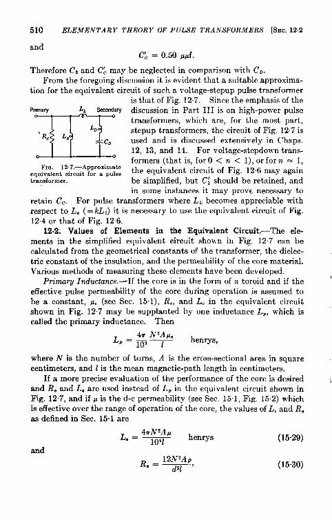
510 ELEMENTARY THEORY OF PULSE TRANSFORMERS [SEC. 12.2
andc; = 0.50 #pf.
Therefore CS and C; may be neglected in comparison with C..From the foregoing discussion it is evident that a suitable approxima-
tion for the equivalent circuit of such a voltage-stepup pulse transformeris that of Fig. 12.7. Since the emphasis of the
Pnmav L~ %condafy discussion in Part III is on high-power pulse
m
transformers, which are, for the most part,L~ stepup transformers, the circuit of Fig. 12.7 is
‘ Re LeCD used and is discussed extensively in Chaps.
12, 13, and 14. For voltage-stepdown trans-formers (that is, for O < n < 1), or for n = 1,
F1cJ. 12.7.—Approximateequivalentcircuitfor a Pulse the equivalent circuit of Fig. 12.6 may againtransformer. be simplified, but C: should be retained, and
in some instances it may prove necessary toretain C,. For pulse transformers where L’ becomes appreciable withrespect to L, ( = kLJ it is necessary to use the equivalent circuit of Fig.12.4 or that of Fig. 126.
12.2. Values of Elements in the Equivalent Circuit.—The ele-ments in the simplified equivalent circuit shown in Fig. 12.7 can becalculated from the geometrical constants of the transformer, the dielec-tric constant of the insulation, and the permeability of the core material.Various methods of measuring these elements have been developed.
Primary Inductance. -If the core is in the form of a toroid and if theeffective pulse permeability of the core during operation is assumed tobe a constant, p, (see Sec. 15.1), R., and L. in the equivalent circuitshown in Fig. 12’7 may be supplanted by one inductance LP, which iscalled the primary inductance. Then
~ = &r N=ApeP 109 1 henrys,
where IV is the number of turns, A is the cross-sectional area in squarecentimeters, and 1 is the mean magnetic-path length in centimeters.
If a more precise evaluation of the performance of the core is desiredand R, and L. are used instead of LP in the equivalent circuit shown inFig. 12.7, and if p is the d-c permeability (see Sec. 15.1, Fig. 15.2) whichis effective over the range of operation of the core, the values of L, and R.
as defined in Sec. 15.1 are
and
~ = 41rN2Ap* ~091 henrys (15.29)
~ = 12N’Ape dll ‘ (15.30)

SEC. 12.2] EQUIVALENT CIRCUIT 511
where p is the resistivity of the core material in ohm-centimeters, and dis the thickness of the lamination in centimeters.
A still more precise equivalent circuit for the core is a ladder networkof LR-rungs, infinite in number, but this circuit is too complex to be ofany practical use and, therefore, either the L, and R. parallel elements orthe L, element in the equivalent circuit is used to represent the core.
Measurement of Lg, or of L. and R., is performed by applying thevoltage pulse from a pulse generator to the primary or secondary ter-minals of the transformer (with the other terminals open-circuited) insuch a way as to simulate the actual operating conditions of the trans-former with regard to voltage, pulse duration, and reverse current, andby measuring the exciting current i~ on a synchroscope as shown in Fig.12.8.
In general, the shape of the trace maybe approximated by the sum ofa rectangle and a triangle, if the initial oscillations are neglected, and the
[a)FIG.12. S,—Method of measurement of primary inductance.
effective shunt resistance R. and inductance L. may be determined asshown in Fig. 12.8. However, if R. > 10L,/T, i.,, for practical purposes,
is negligible in comparison with iL, at t = T. The effect of L. and R. may
then be approximated by the primary inductance L,, determined asshown in Fig. 12”8b.
If the transformer is rated to operate with a reverse current betweenpulses, the circuit shown in Fig. 1208c must be used in the measurement ofL, (or L. and R.), and the pulse generator should be of approximately thesame design as the one with which the transformer is to be used.
Leakage Inductance. -Formulas for the calculation of leakage induct-ance for coils of almost all shapes and types may be obtained from manydifferent sources. This discussion of leakage inductance is confined towindings of the type commonly used in power-output pulse transformers.
Most pulse transformers for regenerative pulse generators and inter-state work have very simple singl~layer, noninterconnected windings,and the calculation of the leakage inductance is very simple. However,many of the pulse transformers that have been evolved have been usedto pulse the cathode of an oscillator tube. To accomplish this purposeseveral different types of winding arrangement have been used.

512 ELEMENTARY THEORY OF PULSE TRANSFORMERS [SEC.12.2
In order to simplify the measurement of oscillator current, the second-ary windings of output transformers are isolated from the primary wind-ings with respect to direct current. Furthermore, in order to supply theoscillator filament current through the pulse transformer from a low-voltage-insulated filament transformer, two secondary windings that areisolated from each other with respect to direct current are provided. Thetwo secondaries are identical and are usually separated from each otherby a minimum amount of insulation; thus they are closely coupled as faras pulses are concerned. A portion of each secondary winding equal tothe primary in number of turns may be placed near the primary windingin a similar fashion; the resultant close coupling makes such a transformerthe equivalent of an autotransformer for pulse conditions.
The simplest type of winding consists of a one-layer primary (low-voltage) winding and a one-layer secondary (high-voltage) winding. Asecond type consists of a one-layer primary and a secondary broken intotwo equal layers, both outside the primary. (Or, the secondary may bebroken into three or more layers.) A third general type consists of aprimary interleaved between two equal layers of a secondary. Two two-layer coils can be put on the two legs of a transformer, and (1) the pri-maries and secondaries both connected in parallel, (2) the primaries andsecondaries both connected in series, or (3) the primaries connected inparallel and the secondaries in series. Two-leg variations on the secondand third general type can also be constructed. Each of the above wind-ing arrangements can be constructed as an isolation (or “ iso”) or an“auto” version (that is, iso or auto for pulse operation).
The calculation of leakage inductance as a lumped parameter followsthe process of reasoning wherein a given amount of load current Z isassumed to be flowing in the coils and the total magnetic energy resultingfrom this load current is computed and equated to $LLZZ. In computingthe leakage inductance of a transformer on this basis the first example tobe considered is a transformer with a one-layer primary and a one-layersecondary of equal length. Since the primary and secondary ampere-tums are approximately equal in magnitude, and since the currents flowin opposite directions around the core, the field between the two windinglayers is very nearly equal to that within a solenoid having the samenumber of ampere-turns. Since the length of the coil is usually large incomparison with the distance between layers, the solenoid may be con-sidered infinite in length, and practically all of the energy in its magneticfield may be considered to be inside the solenoid. Such a solenoidproduces the interlayer field distribution shown in Fig. 12.9b, sincep = 1 both in and between the winding layers.
Actually, the current density is not uniform across the layer thickness.Two extreme conditions of current distribution in the wire that might be

SEC.12.2] EQUIVALENT CIRCUIT 513
used for purposes of computation are (1) the condition where the currentis concentrated in two very thin layers, one at the outside of the insidewinding layer, and the other at the inside of the outside winding layer,and (2) the condition where the current isconcentrated in a very thin layer at the centerof each winding layer. The first extremegives a factor of O in the last term of Eq. 12.1,and the second a factor of ~, instead of thefactor of ~ obtained in the following dkcussionin which a uniform distribution is assumed.Since the conditions usually encountered inpulse transformers lie between these two ex-tremes, and since the layer thickness is usuallymuch smaller than the dktance between layers,the assumption of uniform distribution doesnot produce much error.
The magnitude of H in oersteds (and there
(b)Fm. 12.9.—Distributions
of the magnetic field betweenthe primary and ~econdarywinding layers for 8 simplewinding.
fore of 23 in gauss) is given by the following expressions:4rN~P ZP 4mN,I. z,
In the primary: HI = ~— = — —s
oersteds, where xv isap aP
measured from the side of the primary next to the core; a= is the thicknessof the primary layer in cm; iVP is the number of turns on the primary,N, on the secondary; I, k the primary current in abamperes, I, is thesecondary current; s is the winding length in cm.
kN,I,Between layers: Hz = ~.
4rN.I.In the secondary: Ha = ~
()1 – ~ J where z, is measured from
the inside of the secondary.The energy in a magnetic field in air (p = 1) is given by
W = # ergs/cma,
where His in oersteds. Therefore, the energy stored in the leakage fieldis given by
(/
w_ll& a’
“’ZP--H’A+[H”Z)
=ZU+’Y[U3’’,’A+ [(1-:Y”ItiN:I:u.
J3 ()A+.?:,
where cu is the average circumference of the layers in centimeters, A is

514 ELEMENTARY THEORY OF PULSE TRANSFORMERS [SEC.12.2
the distance between layers in centimeters, and 2a is the sum of thethicknesses of the layers. Since the energy stored in an inductance is
given by W = ~LI’, the following equa-tion may be solved for the leakage induct-ance, referred to the secondary:
~1, ; LJ: =%rN:I:u
2 ()A+:.
a8z
# L From this equation,
47rN;LuL==T
()A+% abhenrys. (1)
The second example to be considered(b)
Fm. 12. 10.—Distribution of theis a transformer with a one-layer primary
magnetic field for a coil with a and a secondary composed of two equalsingle-layerprimaryand a double- layers, as shown in Fig. 1210. The fluxlayersecondarywinding. distribution is shown in Fig. 12.10b, andthe magnitude of H is given by the following expressions:
4uN~p Z, 4rN.1, z,Inpnmary: HI = ~— = ——.
aP J3 aP
4uN,I,In first interlayer space: Hz = ~.
41rN81,In first secondary layer: Hs = ~
()2–5.
aa.,-4rN,I.
In second interlayer space: H4 = ~.
4UN,I,In second secondary layer: Hs = ~
()l+’.
In these expressions z,, z.,, z,, are measured from the inside of the
primary, and of the first secondary and second secondary layers,respective y.
The energy in the field is given by
(2)

SEC.122] EQUIVALENT CIRCUIT 515
The third example to be considered is a transformer with a single-layer primary interleaved between two equal layers of a secondary, asshown in Fig. 12.11. From the flux-density distribution across the coil(indicated in Fig. 12.llb) it may be seenthat the transformer can be divided intotwo equal parts by a line drawn throughthe center of the primary and each parttreated as a simple two-layer transformer.The total energy stored is the sum of theenergies in the two parts, and the leakageinductance is given by
( A, a.,+ ati+z+iz )1
abhenrys. (3)
+ Is
NPIP
(b)
Fm. 12.11.—Distribution of themagnetic fieId for a primarywinding interleaved between twosecondary-windings.
If a simple two-layer transformer is comected as an autotransformer,the number of turns in the outer layer is N, (n – 1)/n, where n is thestepup ratio, and the number of ampereturns is N,I. (n – 1)/n. Thecurrent in the inner layer is lP(n — 1)/n, and the number of ampere.turns is NplP(n – 1)/n, which is equal to NJ.(n – 1)/n. Therefore,the field between the windhgs is reduced from that in the iso type bythe factor (n – 1)/n, and the energy by the factor [(n – I)/n]*. Thus.
‘.=4*R+2(A+3 (4)
The expressions for the leakage inductance of the auto versions of morecomplicated types of winding arrangement are the expressions for the isoversions multiplied by this factor [(n — 1)/n]z.
These equations have been applied to the specific types of windingsdiagramed in Figs. 12.12 and 12.13, and the values of the leakage induct-ance recorded in Table 12.1.
Measurement of leakage inductance can be performed by either apulse method or a steady-stage method. The circuit that is shown inFig. 12.14a and by which the increase of current through a st:mdaniadjustable calibrated inductance L. is compared and adjusted to coincidewith the increase of current through LL produces a s.ynchroscope traceof the type shown in ~lg. 12. 14b. The value of L L is then determined by
the setting of the standard inductance.
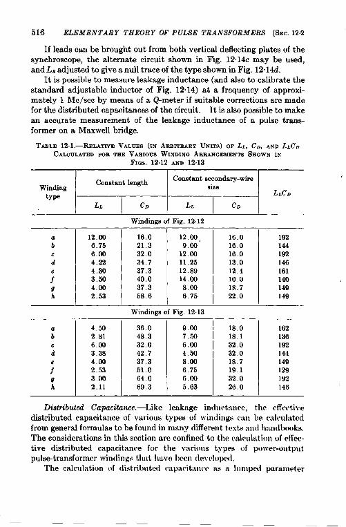
516 ELEMENTARY THEORY OF PULSE TRANSFORMERS [SEC. 12.2
If leads can be brought out from both vertical deflecting plates of the
synchroscope, the alternate circuit shown in Fig. 12”14c may be used,and La adjusted to give a null trace of the type shown in Fig. 12. 14d.
It is possible to measure leakage inductance (and also to calibrate thestandard adjustable inductor of Fig. 12.14) at a frequency of approxi-mately 1 Me/see by means of a Q-meter if suitable corrections are madefor the distributed capacitances of the circuit. It is also possible to makean accurate measurement of the leakage inductance of a pulse trans-former on a Maxwell bridge.
TABLE 12.1 .—RELATmE VALUES (IN ARBITRARY UNITS) OF L~, CD, AND L~CD
CALCULATEDFORTEEVARIOUSWINDINGARRANGEMENTSSHOWN IN
FIGS. 12.12 AND12.131 I 1
Constantlength Constantsecondary-wireWinding size
type L~CD
LLI
cD LLI
cll
ab
c
d
;
9h
12.006.756.004.224.303.504.002.53
Windingsof Fig. 12.12
16,0 12.00, 16.0 19221.3 9.00 16.0 14432.0 12.00 16.0 19234.7 11.25 13.0 14637.3 12.89 12.4 16140.0 14.00 10.0 14037.3 8.00 18.7 14958.6 6.75 22,0 149
Windingsof Fig. 12.13
a 4.50 36.0 9.00 18,0 162b 2.31 48.3 7.50 18.1 136c 6.00 32.0 6.00 32.0 192d 3.38 42.7 4.50 32.0 144
4.00 37.3 8.00 18.7 149
; 2.53 51,0 6.75 19.1 1299 3.00 64.0 6.00 32.0 192h 2.11 69.3 5.63 26.0 146
Distributed Capucdance.-Like leakage inductance, the effectivedistributed capacitance of various types of windings can be c:dculatedfrom general formulas to be found in many different texts and handbooks.The considerations in thk section are confined to the calcuh~tion of etTec-tive distributed capacitance for the various types of power-outputpulse-transformer windings tlmt have been developed.
The cahmlation of distributed capacitance as a lumped parameter
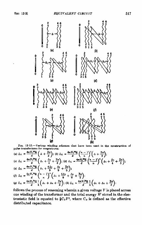
SEC. 12.2] EQUIVALENT CIRCUIT
2 460
1{/
A
01 35(a) d ~
20
IIN
Al
oi 3s
(c)2
[!
460
A
135 (e)
2 460
IIN
A, AZ
o35 I
(9)
2 40
N
A
o315
2(b) ~ c
o
0315
(d2 46
0
Io
315W
2 460
10
315
(MFm. 12. 12.—Various winding schemes that have been used in the
pulse transforrnera for magnetron:
‘a)” “4+%(’ +:)’ ‘b)” -4+U(%)’(A+%)’
517
c.onntruatiouof
follows the process of reasoning wherein a given voltage 1’ is placed acrossone winding of the transformer and the total energy W stored in the elec-trostatic field is equated to ~C~Vz, where CD is defined aa the effectivedistributed capacitance.

518 ELEMENTARY THEORY OF PULSE TRANSFORMERS [SEC. 12.2
2 46 2 46
(a)315
Two legsconnectedinseries (b)
!’1::IA!IM:;M “35 1
(d315
Two legsconnectedmparallel(d)
35 0;0
(e)Primaries inparallel,
secondaries m series Ul
6 2 44 2 6
b) (h]
Fm. 12. 13.—Various winding schemes tpulse transformers for magnetrons:
that have been used in the construction of
(a) ~L = 4~~a*’u 1— -.C4 ( )
A~+AB+~ ;(fJ)L~=4+W+(”%2(XA +%)’
4TN,~~ 1
((C) LL=rz A~+A~+~
)—Z(y) (.A+$);;(d)L~=4TN.2111 n–l 2
(e) ~L = 4~~#11 1s i—(
A.+ AB+~ ;(f)LL =4~w~(~)’(XA +~);)
~, LL = 4zN,*ll 1e ( )’
(h) LL =4’$373? +%)”
The capacitance of a parallel plate capacitor, each of whose electrodesis an equipotential surface, is given by the relation
Co= 0.0885 ‘“l “~o-’z farads, (5)

SEC. 12.2] EQUIVALENT CIRCUIT 519
v (5OO-1OOOv)
-ir
*
Commutator
L~ HvI
Lv
To CRT
i-R
v (5OO-1OOOV) z (a)
*LsralLv(c) (d)
FIG. 12. 14.—Method of measurement of leakage inductance. (Note: Ls should be wound sothat it has a low distributed self-capacitance and a low stray capacitance to ground.)
which can be found in most handbooks of electrical engineering, and theenergy stored in a capacitance is given by
w = +COV2 joules.
A pulse transformer with two adjacent winding layers of circumferenceu and length s may be considered as a con-denser composed of two plates of area w cm’ ‘B’
v.%
and separation A cm. Because of the pulsevoltages developed across the windings, the
Tl jvxlplates of this condenser can no longer be t. ‘“ J------------
considered as equipotential surfaces, and the I ‘---------- Tvoltage distribution along the windings mustbe taken into consideration in the computation l-t-’-iiof the effective distributed capacitance. The
vAI vA2
energy stored in a section of width LUand FIG. 12.15.—Voltage at
height dx (see Fig. 12.15) k given byvarious points on a two-layercoil.
( )dW = ~ 0.0885 ~ dx (6V.)2 . I&’z joules,
where c is the dielectric constant of the material between the plates.
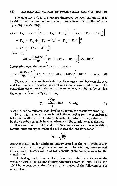
520 ELEMENTARY THEORY OF PULSE TRANSFORMERS [SEC.122
The quantity 6V. is the voltage difference between the platea at aheight z from the lower end of the coil. For a linear distribution of volbage along the windings,
[ 1[~v.= v., – v., = vA, + (V,, – v.) ; – V~, + (v., – V.) ~ 1
[ 1= v., – VA, + (V,, – v,> – (VA, – VA,) ;
= 6VA + (6VB – 6~A) ;-
Therefore,
~W = 0.0885#u2A [ 1
6VA + (6VB – 6V.J : z dz . 10_l*.
Integration over the range from O tos yields
~ = 0.0885#u Q
2A [ 1~ (bv.)’+ ~~.. 6V. + (6VB)2 “ 10-’2 joules. (6)
This equation is used in calculating the energy stored between the coreand the first layer, between the first and second layer, and so on. The
equivalent capacitance, referred to the secondary, is obtained by solving
2the equation W = ~CDWJ, that is,
(7)
where Vz is the pulse voltage developed across the secondary winding.By a rough calculation made with the equation for the capacitance
between parallel wires of infinite length, the intertum capacitance canbe shown to be negligible in comparison with the interlayer capacitance.
It is shown in Sec. 13”1 that, if L.C. equals a constant, one conditionfor minimum energy stored in the coil is that the load impedance
Another condition for minimum energy stored in the coil, obviously, isthat the value of LACD be a minimum. The winding arrangementthat gives the lowest values of LLCD should therefore be chosen for thetransformer.
The leakage inductance and effective distributed capacitance of thevarious types of pulsetransformer windings shown in Figs. 12.12 and12.13 have been calculated for n = 4, with each of the following sets ofassumptions:

SEC.12.2] EQUIVALENT CIRCUIT 521
1. The thickness of each insulating pad is proportional to the maxi-mum voltage applied across it, and the coil length is the same forall types, but the wire size is variable.
2. The thickness of each insulating pad is proportional to the maxi-mum voltage applied across it, and the secondary wire size is thesame for all types, but the coil length is variable.
Values of LL and CD (in arbitrary units) calculated with each of the abovesets of assumptions and values of the product LK7D are given in Table12.1. Since the product LLCD is independent of the length of the wind-ing for a given type, it is the same for both sets of assumptions. Thethickness of the winding layers is assumed to be small in comparison withthe thickness of the insulation between layers, and is therefore neglectedin these calculations.
The results given in Table 12.1 show that all of the auto types havelower values of the product LLCD than do any of the iso types, althoughthe value for the highest auto type is identical with that for the lowestiso type. The lowest and highest values for the auto types differ byonly about 15 per cent. [Note: If the thickness of insulation betweeninner winding and core is doubled, the iso types are improved somewhatin comparison with the auto types; also type (h), Fig. 12.12, is improvedrelative to the other auto types, whereas type (f) becomes relatively poor.Types (j) and (b), Fig. 12.13, still appear to be the best.]
The insertion of an electrostatic shield between the primary and thesecondary results in an appreciable increase in LLCD, and is thereforerecommended only where it is absolutely necessary that the directcapacitive coupling between primary and secondary be eliminated.
The preferred method of measuring the effective distributed capaci-tance of pulse-transformer coils depends upon the type of winding. Fortransformers with simple one-layer windings, the value of the distributedcapacitance may be obtained by measuring the capacitance betweenwindings at 60 or 1000 cycles/see and applying a factor that dependsupon the distribution of voltage on the windings during the pulse. I
The self-capacitance of an individual duo-lateral winding can beobtained by measurement, by standard methods, at frequencies approxi-mately equal to the highest important frequencies contained in the pulse.For transformers that employ special interleaving or interconnecting tominimize the product of leakage inductance and distributed capacitance,the circuit of Fig. 12.16 may be used to compare the capacitance currentin the lower-voltage winding with the capacitance current in the adjust-able equivalent circuit. The inductor L: and the resistor R: are inserted
1See Sec. 14.2 for a discussionof the calculation of thii factor for regenerativepulsegenerator.

522 ELEMENTARY THEORY OF PULSE TRANSFORMERS [SEC. 12.2
to simulate the magnetizing current in the transformer and are adjustedfirst to give a trace which coincides with that of the transformer afterthe capacitance currents have subsided (that is, toward the latter partof the pulse). The values of Lj and CL are then adjusted to give acapacitance-current spike which coincides with that of the transformerat the beginning of the pulse. The value of CD may then be read fromthe setting of CL, and the value of L. from the setting of L;. This valueof LL is referred to the lower-voltage winding; the previously describedmethod of measuring L. gives greater precision since in that method themeasured value is referred to the higher-voltage winding and is thereforenumerically larger.
G V(5CO.1OWV)
m
L’~Hv LV
Commu-
11 ~to’z R; ~:e
CRTR
currentthrough Le/ and R. alonevt—-..‘1 ‘ ‘- --2-‘“\ Current inthe
equivalentcircutiCurrentinthe afteradjustmenttransformer \ Current in the
equivalent circuit&fore adjustment
ja) (b)‘FIG. 12. 16.—Method of measurement of distributed capacitance. (Note: L~’ should be
wound so that its effective distributed capacitance is low.)
The effective distributed capacitance of a pulse-transformer windingcan also be measured by means of an r-f bridge. 1
Characteristic Impedance of a Pulse Transformer.—It is shown in
Sec. 131 that _ may be thought of as a characteristic impedanceof a winding for a transformer that may be represented by the equivalentcircuit of Fig. 12.7. For a simple coil with a one-layer primary and aone-layer secondary winding of equal length, and with negligible winding-layer thickness,
(8)
and0.0885cu~f, ~ ~o_12
CD = jlco = ~ farads, (9)
where Co is calculated by the use of Eq. (5), and f, is a fraction dependingupon the voltage distribution between the primary and the secondary.
1For example,see P. R. Gillette, “ PulseTransformerCommittee,ProposedBasicSpecificationsfor PulseTransformers,” RL Report No. SS1,Nov. 8, 1945.

SEC. 12.2] JWJ.!JIVA LEN7’ CIRC(JIT 523
Then the characteristic impedance is
J ‘--~= 377N.A
“ = CD ohms.J3 V@
(lo)
The concept of characteristic impedance is, however, more meaningfulwhen applied to circuits with distributed rather than lumped parameters.A simple example of a circuit having distributed inductance and capaci-tance and a characteristic impedance ZO is one composed of two longparallel strips of conducting material, 1 meter wide and 1 meter apart,which are part of two conducting sheets infinite in extent. 1 If thepermeability and dielectric constant of the material betwe~n the sheetsare respectively pl and c1in mks units, it can be shown that, for a planeelectromagnetic wave propagated between the two strips,
‘o=s=&=8&=$377 ‘hms
where PO and COare, respectively, the permeability and the dielectricconstant of free space in mks units, and 377 ohms is the characteristicimpedance of free space.
If the spacing between the strips is reduced to A meters and the widthof the strips becomes & meters, and P = 1,
z, = L 377 ohms,s de
and & and A may be measured in cm or meters.If these parallel strips are now wrapped into two concentric cylinders
whose circumferences are large compared with the distance A between thecylinders, and whose length iss, the characteristic impedance for a planeelectromagnetic wave traveling circumferentially in the space betweenthe two cylindem i.s still equal to (A/A3 WC) 377 ohms.
If the outer and inner cylinders are now slit helically so that theybecome coils of N, and N. turns respectively, and the electromagneticwave is ushered in at one end of the coil and out at the other end, theinductance per unit length of circumference is greater by a factor of N:(for the secondary) than it is for the unslit cylinders. The capacitanceper unit length of circumference is different by a factor of fl, dependingupon the particular type of voltage distribution that is set up betweenthe primary and secondary. Therefore, the characteristic impedance ofthe secondary winding may be expressed by
z’ = = 377 ohms.J3&l
I J. C. Slater,MicmwaceTransmission, McGraw-Hill, New York, 1942,p. 98.

524 ELEMENTARY THEORY OF PUL,TE TRANSFORMERS l%c. 12,2
The characteristic impedance between the two plus (or the two minus)terminals of primary and secondary of a transformer with a simple wind-
1$’~!:Wh!ding
No.2 ~ Smallviewingrew.tance
Fm. 12. 17.—Circuit for measuring thecharact.eriatio impedance of a pulee-trans-former coil with eingle-layer primary andsingfe-layer se~ndary of equal length, andwith n = 1.
ing, such as that of the above ex-ample, whose stepup ratio is unitycan be measured by the techniquessimilar to those used in the imped-ance measurements of pulse-form-ing networks (see Sec. 6.6). Ifpulses are applied between thesingle-layer primary and the single-layer secondary of a 1/1 trans-former, as indicated in Fig. 12.17,the voltage waveforms at points
A, B, and C are as shown in Fig. 12.18, where 6 is the time takenfor an impulse to travel along the wires from one end of the coil to the
‘Wc(a) R,= co
f--l..yI
F
Bc
28 A
‘v(c) R, =2,
FIG. 12.18.—Drawingsof synchroscopetracesobtainedat pointsA, B, andC in the circuitof Fig. 12.17 for three different values of R!.
other. When the value of Rl k so adjusted that the trace of Fig. 12.18c isobtained, the value of Rl is equal to the value of the characteristic

SEC. 12.2] EQUIVALENT CIRCUIT 525
impedance Z.. For a transformer of this type the values of 2, obtainedby this method of measurement and by the method of calculation pre-viously described agree within a few per cent.
The small oscillations appearing at the very beginning of the pulseon traces B and C, Fig. 12.18, are the result of turn-to-turn transmissionof the impulse. The impulse thus transmitted travels from one end of thecoil to the other much more rapidly than the impulse which must travelalong the wires.
If a 1/I transformer is wound symmetrically on two legs of the core,small oscillations appear in the middle of the steps. These oscillations. .are the result of small reflections that occurwhere the two coils are connected. Pulsetransformer111and1/3
PulserFor windings of a more complicated
nature the characteristic impedance of partof the winding may be different from that of
@j pganother part of the winding. Also, if n > 1, =%the measurement of impedance becomes =Small 40 = Small
vieMng vitwingmuch more difficult to perform. Figure reswancs resistsnm
12.20 shows some drawings of synchroscope Fm. 12.19.—Circuitused forpulsing two transformers, one
traces obtained at various points in the ~it~ ~ = ~, the other withcircuit of Fig. 12”19, in which a transformer n = 3, to obtain the traces
with n = 1 and a transformer with n = 3, ‘hewn ‘n ‘is” 12”20”
const rutted to have the same Z~ (1200 ohms) for the secondary (high-voltage) winding, were pulsed in turn with various loads attached.
It can be seen from these traces that the general character of thetransmission delay of the transformer with n = 1 is retained by the trans-former with n = 3, but that the tops of the steps of the latter are slantinginstead of horizontal and that oscillations whose period is either i 6 or*6 often appear on these slanting tops. A simplified explanation isthat the sloping tops of the steps are the result of charging an effectivedistributed capacitance through the characteristic impedance Z. of thetransformer winding.
It is interesting to note the nature of the approximation wherein theeffect of distributed inductance per unit length of the wire is replaced bya lumped-parameter leakage inductance in the equivalent circuit. ForR, = O and for R. almost equal to O, the slope of the average of trace D
shown in Fig. 12.20d is Va/~Z~, where 6is the time necessary for an electr~magnetic impulse to travel along the secondary winding from one end ofthe coil to the other. If S is the total length of the wire, and if L and Care respectively the inductance and capacitance per unit length of thewinding,
6= SGC,
(z, = ;,

526 ELEMENTARY THEORY OF PULSE TRANSFORMERS [SEC.12.2
and the slope of the average of trace D (Fig. 12”2W) is VQ/LS = Va/LL
where LL = LS. This slope VG/LL k simply the rate at which currentincreases when it is limited by the lumped-parameter l~akage inductance.
For multilayer-winding and duolaterally wound transformers theconcept of characteristic impedance from the point of view of distributedparameters becomes more and more strained. The characteristic imped-
-IiE=+ 28-’ :“,, ,-. + cmo ‘“- 1/3&.’ 1.-,~)---..- ,’.’ -e-----,. -----
B
‘6
1/1‘B
(a) RI= m
F
K,,
+ 26A
;;o . . .... ,-,-, t- 173
c1’
,----.
D
(c) RI =0, high powar-supply voltage
(f)) RI= 1200 ohms (d) RI =0, low iower-supplyvoltage
FIG. 12.20.—Drawings of oscilloscope traces obtained at the various points of the circuitshown in Fig. 12.19 for transformers with n = 1 and n = 3, (a) with RI = m, (b) withRi = 1200 ohms, which, for the secondaries of both transformers, is equal to the value of
NA— 377ohms,and(c) and (d) with RI = 0.ZT calculated from Z~ = ~ ~~
antes can then be best thought of as equal to ~LL/CD, where LL ancl
CD are lumped parameters.Churp”ng Inductance. -When a pulse transformer is operated into a
load of low dynamic impedance (for example, a magnetron), oscillationswhose period is usually considerably less than % _ often appearon the top of the current pulse. These oscillations may be considered tobe the result of the transmission and reflection in the coil of disturbancesthat are probably initiated at the end of the secondary to which theoscillator is attached. The impedance of the secondary winding to the

SEC. 12.2] EQUIVALENT CIRCUIT 527
transmission of such disturbances is
N.A— 377 ohms..13~,
The time taken for the disturbance to travel along a length of secondarywire of N: turns to the first discontinuity in the impedance is
where ‘U is the mean length of turns of the secondary winding in centi-meters, c is the velocity of light in centimeters per second, and N; is thenumber of turns on the secondary winding between the high-voltage endand the first sharp discontinuity in impedance (~, of course, is equal tounity for the space between the coils). The time transpired before thisdisturbance is reflected back to the source is 28, and when, upon succes-sive reflections that set up shock-excited sbnding waves, the fluctuationsof voltage and current at the source take on the approximate sem-blance of a sine wave, the period T of the fundamental of these oscillationsis either 26 or 46, depending upon the nature of the discontinuity inimpedance. The effect is somewhat analogous to the two differentfundamental periods of oscillation that are set up in closed and openorgan pipes.
Figures 12.18 and 12.20a show examples of such sine-wave oscilla-tions occurring in the operation of the circuits of Figs. 12.17 and 12”19respectively.
Figures 2.44 and 2.45 show such sin~wave oscillations appearing onthe current pulse in a magnetron. The fundamental period of theseoscillations is usually
T =28= ‘N:w 4,c
and the periods of various harmonics are integral divisions of this period.The periods thus calculated agree with the periods of oscillation observedif there are no interfering effects resulting from capacitance across theprimary winding. For each discontinuity in impedance along the coilthere is observed among the oscillations sine-wave components of afundamental period corresponding to each of the resulting reflections.
In the equivalent circuit for a pulse transformer and a biased-diodeor magnetron load (Fig. 12”7) the effect of these reflections can, to a crudeapproximation, be taken into account by inserting in series with CD aninductance L. such that
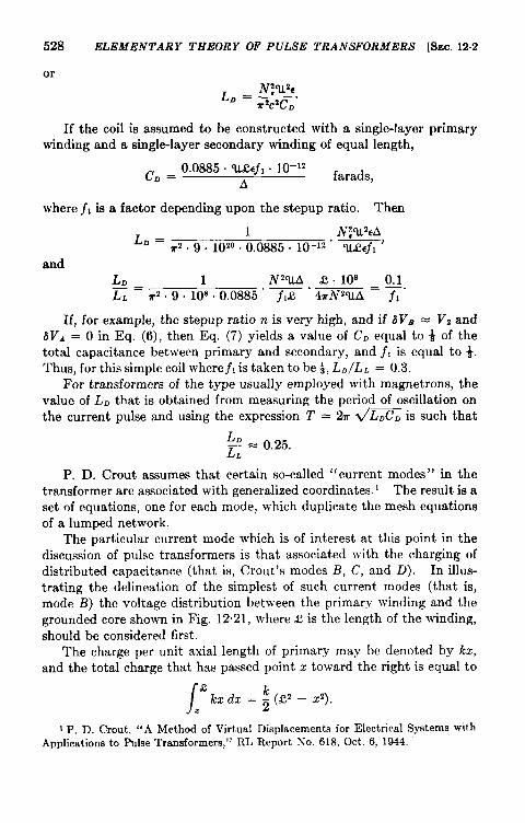
528 ELEMENTARY THEORY OF PULSE TRANSFORMERS [SEC.12.2
or
L. =e.
7r2c2CD
If the coil is assumed to be constructed with a single-layer primarywinding and a single-layer secondary winding of equal length,
c. =0.0885. ‘u&j, . 10–12
farads,A
where jl is a factor depending upon the stepup ratio. Then
L. =1 . N:u2eA,
mz09.1020.0.0885. 10_lz ‘u&j,
andL. 1 N“uA s .10’ 0.1G= T’.9 .10’ .0.0885 “ ~ “ -A = ~-
If, for example, the stepup ratio n is very high, and if ~VB = Vz and6V~ = O in Eq. (6), then Eq. (7) yields a value of CD equal to i of thetotal capacitance between primary and secondary, and j, is equal to i.Thus, for this simple coil where j, is taken to be %,L~/LL = 0.3.
For transformers of the type usually employed with magnetrons, thevalue of L~ that is obtained from measuring the period of oscillation onthe current pulse and using the expression T = % V’JCJDC.issuch that
P. D. Crout assumes that certain so-called “current modes” in thetransformer are associated with generalized coordinates. 1 The result is aset of equations, one for each mode, which duplicate the mesh equationsof a lumped network.
The particular current mode which is of interest at this point in thediscussion of pulse transformers is that associated with the charging ofdistributed capacitance (that is, Crout’s modes 1?, C, and D). In illus-trating the delineation of the simplest of such current modes (that is,mode l?) the voltage distribution between the primary winding and thegrounded core shown in Fig. 1221, where s is the length of the winding,should be considered first.
The charge per unit axial length of primary may be denoted by h,and the total charge that has passed point z toward the right is equal to
I P, D. Crout, “A Method of Virtual Displacementsfor Electrical SystemswithApplicationsto PulseTransformers,” RL Report No. 618, Oct. 6, 1944.

Ezc. 12.2] EQUIVALENT CIRCUIT 529
In order that the mode may produce no net mmf on the core, it is requiredthat there flow in the opposite direction in the primary winding a currentwhich is constant along the primary and whose mmf cancels that of thecurrent flowing toward the right. Since the number of turns per unitlength is constant along the primary, thedesired average current flowing towardthe left is k&2/3.
Then, if the primary current outsidethe wi.rdhg is denoted by @B/eit (seeFig. 12.21 b), k = q., and the primarycurrent in the winding (positive for flowto the left) is
dq,
2% ‘s’ -“)%—.—dt
The displacement current from primary tocore per unit length of winding is 3z/z2dq~/dt.
As q, is varied it is evident that thisso-called “mode B” has the followingproperties:
1. No mmf acts upon the core.2. The primary winding behaves as
an autotransformer to charge theprimary-to-core distributed capac-itance with a linear voltagedistribution.
.-
3? —————I———— ——
~d A
B
0
0 %-- 1-44,
dl (c)
FIG. 12.21.—(a) Voltage dis.tr-ibution between primary andcore for a pulse tranaf ormer.
(b) Displacement current flow-ing bet ween primary and core.
(c) Plots of displacement andnet primary currents. Curve A isthe displacement current from pri-mary to core per unit length ofwinding, Curve f3 is the net primarycurrent.
The displacement current per unit length of winding and the netprimary current are plotted in Fig. 12 .21c. It is evident that at allpoints except one along the length of the coil the net primary current isdifferent from zero (although the net mmf on the core is zero). Theenergy stored in the magnetic field associated with this primary currentmay be represented to a first approximation by an inductance in serieswith the effective distributed capacitance in the equivalent circuit(whence L. in Fig. 12.6).
By the same process of delineation of current modes it may be shownthat, to a first approximation, an equivalent inductance L. may be placedin series with the effective distributed capacitance CD existing betweenthe primary and the secondary (see Fig. 12.6).
Thus, where there is a voltage distribution that increases along the

530 ELEMENTARY THEORY OF PULSE TRANSFORMERS [SEC. 12.2
length of the coil between primary and core, or between secondary andprimary, there are capacitance currents that flow in such a way thatmagnetic fields (“squirted” flux) are created outside the coil as well aainside. These fields, obtained with a combination of a transformer withn = 3 and the circuit of Fig. 12”19-a combination that is pulsed at atime t = O for a duration>> &-and observed in the axial direction of thecoil with a magnetic probe and a synchroscope, are shown for variouspositions along the coil in Fig. 12 “22a. It is obvious from the tracesthat both fundamentals and harmonics exist in the time variation of themagnetic fields associated with charging currents. A plot Of ValUeS Ofthese fields for the first and second harmonics has been constructed inFig. 12.22b, and a rough schematic pattern of these fields about the coil
FM harmonic
*
!@’&“k --(a)
firstharmonic
i= --r.—-—.—.f.engthof coil
(c)Fm. 12.22.—(a) Drawings of synchroscope traces showing the intensity of the magnetic
field in the axial direction obtcined with a magnetic proba at various points clong the coil.(b) Plot of the distribution clong the coil of the paak magnetic fielde of the first and
eecond harmonica that occur in the time variation of tbe aquirtcd flux.(c) Rough schematic plot of the field patterne for the first and second harmonics.
for the first and second harmonics has been drawn in Fig. 12022c. Thecharging inductance LD (or several LD’s, one for each harmonic) may beintroduced into the equivalent circuit to take into account the energythat is stored in these magnetic fields when charging currents flow inthe transformer coil.
There is no contradiction between the concepts of transmission-reflection and squirted flux, as they are merely different aspects of thesame phenomenon, a phenomenon which is similar to the oscillationsthat occur in an organ pipe or along a vibrating string. In all of thesephenomena the reflection of traveling waves sets up sinusoidal displacements in the form of standing waves. The difference between the twoconcepts is that, with a transformer coil in which the voltage distribu-tion is such that the voltage difference increases along the coil, thesquirted-flux theory predicts external magnetic fields of the type shownin Fig. 12.22, whereas the pure reflection theory does not.

SEC.12.2] EQUIVALENT CIRCUIT 531
Summary .—’l’his chapter has given a brief treatment of generaltransformer theory, has indicated a workable equivalent circuit for apulse transformer, has shown how the elements in this equivalent circuitmay be calculated and measured, and has introduced and briefly discussedthe concepts of characteristic impedance and modes of oscillation of apuls-transformer winding.

CHAPTER 13
PULSE-TRANSFORMER DESIGN
BY W. H. BOSTICK
In this chapter, Sec. 13.1 discusses the relationship between theelements in the equivalent circuit and the rated load impedance, ratedpulse duration, and efficiency of a pulse transformer. Section 13.2presents methods of achieving a design that meets the requirements ofspecified load impedance, specified pulse duration, and maximum effi-ciency. Section 133 provides design data for a number of successful
..” ..l
FIG. 13, 1.—Equivalent circuit usedin the consideration of the optimumrelationships among Rt, CD, LL, Le. andR. for e. specified load impedanie andpulse duration.
section form the most rationaltransformers giving maximum transfer of pulse energy to the load.
In developing these relationships, it is helpful to consider the systemof Fig. 13.1 where
V@ is a source voltage,Ro is the source impedance,L. is the effective shunt inductance,R. is the effective shunt resistance,RJ is the load impedance (a resistance),
Cc, which represents the capacitance between the low-voltage wind-ing of a transformer and the core (which is grounded), is gener-ally neglected, and
LLC~ equals a constant (a relationship that is true for a constant meancoil perimeter and a constant number of turns for pulse trans-
pulse transformers covering a waerange of pulse durations and imped-ance levels.
13.1. General Pulse-transformerDesign Considerations.—Many suc-cessful pulse transformers have beendesigned without consideration orcognizance of certain relationshipsbetween the elements in the equivalentcircuit and the transformer ratingand efficiency. It is the author’sbelief, however, that these relation-ships which are dkcussed in this
general basis for the design of pulse
formers).632
SEC. 13.1] PULSE-TRANSFORMER DESIGN CONSIDERATION 533
It is desirable to transfer a maximum of energy to Rl in a giveninterval of time during which switch (1) is closed (that is, the pulse dura-tion 1, which in average design practice is usually considerably greater
than 2U 4LLCD), and hence to transfer a minimum of energy to R., L.
(or LP, see Sec. 12.2), L., and CD. In a treatment of this problem it ishelpful to introduce the quantity a;
Energy flowing into the core during the pulsea = Energy transmitted to the load during the pulse”
Then
where the core is represented by an equivalent circuit consisting of L.
and R. in parallel, and i~ is the magnetizing current that builds up in Le
and R..
If, as is often true, the laminations are very thin, or if the pulseduration is long compared with the time constant of the lamination (seeSec. 15. 1), the core may be approximately represented in the equivalentcircuit by LP, instead of by L. and R,.
Thenv, ,
a = z=,”
It is also useful to define the quantity ~;
Energy stored in leakage inductance anddistributed capacitance during the pulse
P= Energy transmitted to the load during the pulseThen
For a variable winding length and a variable spacing between theprimary and the secondary, L.CD = constant [see Eqs. (12.4), (12.6),and (12 .7)]. A maximum amount of pulse energy is transferred to theload (as far as the coil is concerned) if a minimum amount of ener~ isstored in the coil. Therefore, @ is minimized under the condition thatLLCD = constant.Thus,
d~ 1
(
constant~ = 2V1Zrr 1 – L: “R’)(*)=”
or
(1)

534 PULSE-TRANSFORMER DESIGN [SEC. 13.1
and
:LL(*l)2=tc-’(#%JThis condition for maximum energy transfer might be obtained by wayof a thermodynamical analogy by reasoning that the system would bein its equilibrium state if there were an equipartition of energy betweenthe two degrees of freedom, that is, that
The quantity ~~~, which has the dimensions of impedance, maybe thought of as the transient or characteristic impedance of the LA7.-
network. When the impedance of this network is equal to the loadimpedance, maximum energy transfer to the load is effected.
The resultant value of @ for minimum ener~ stored in the coi~is
For transformers in which the voltage stepup ratio n >2 or n < – 1(that is, transformers for which the equivalent circuit of Fig. 13.1 applies),and which are operated on a resistance load, observation and calculation(see Fig. 1412) of pulse shapes show that pulse shape is approximatelyoptimum when the sum a + 19is a minimum. 1
For stepup transformers operated on a magnetron load, both calori-metric measurement of efficiency and observation of the, shape of thecurrent and voltage pulses show that the efficiency (for fkxl RQ and RJ is
maximum and, in general, the pulse shape and performance are optimumwhen a + @ is a minimum. The value of the pulse duration , at whichthe transformer with a given L., R, (or L=), and CD gives a minimum ofa + @ can be determined as follows:
:(a+tJ)=$[&&+&ii+=’]=o,
If -o=’. lCD2L. -T= ‘
or
7., = dm. (2)
I The criteriafor optimum pulseshape constitutea very controversialsubject. Agood pulse shape k the result of a skillful compromiseamong high rate of rise, lowovershoot, small amount of droop, high rate of fall, and low backswingvoltage. Itie the author’s belief that the most suitable compromise among these quantities isobtained by makinga + p a minimum.

SEC.13.1] PULSE-TRANSFORMER DESIGN CONSIDERATION 535
The quantity a + /3 for T~,,is defined as (a + 13)W,,and
@+ ’)@=E+M”If the effect of R. is neglected,
r2LL(a + f%, = ~
P(3)
-T., = %mz,and if
T = T.Dtff= l?.
Then, at any r such that r/rW, = ~,
a+d=(a+l%lt ();++”Thus, if fi= 2 or ~,
Q’ + 9 = Ha + mow,if f=30r*,
a+~=; (a+l?)o.t,andifj=40r~,
~ + @ = %(@ + P)OD1.
It is obvious that, if the transformer is to be operated over a range ofpulse durations from ,~i. to 7~-,, .~p, should be chosen to be equal to
c.It is of some interest to relate (a + 19)~..to the coupling coefficient k.
From Fig. 12.4 it is apparent that 2(L, – Ml) = L., or
Since
If the transformer is a noninverting transformer with a stepup ration = 1, then CD = O, and no electrostatic, only magnetic energy is storedin the coil. Minimum energy stored as ~L.1~ in the coil is then achieved,
and the relationship RI = ~~ is most nearly approximated whenL. is a minimum.

536 PULSE-TRANSFORMER DESIGN [SEC. 132
The capacitance Cc of the low-voltage winding to core is, of course,always present, and energy is stored in CC. However, Cc does not bearthe close relationship to LL that C’. does, and CC may be kept smallmerely by using adequate winding-t~ore insulation. In properlydesigned pulse transformers, Cc is always negligible compared with C.when n >2 or < – 1. Therefore, the value of Cc is of little significancein design considerations, except for the fact that it is usually kept negligi-bly small.
In addition to C. there is the input capacitance Cl of the load, which isusually smaller than CD. For a system using one transformer, the energystored as ~C~V~ + ~LLI~ for a constant product L~CD is a minimum whenRI = ~~., but the pulse shape is usually optimum (for a voltage-stepup transformer) when R1 = ~ LL/(C. + Cl) (see Sec. 14.1). In a
system using stepdown and stepup transformers separated by a cablewhose transit time is less than V’L~CD, 1 the energy stored as ~C.V~ +24L.I; for a constant product L.CD is a minimum when Rl = ~-i,
but the pulse shape is optimum when Rl = <>L./(C. – Cl) (see Sec.
14.1), where CD is the effective primary-to-secondary capacitance of thestepup transformer. Therefore, a compromise must be struck betweenmaximum efficiency of the transformer or transformers and optimumpulse shape. Because the assumption that ~. should be equal toRI generally gives good results and leads to simpler relationships, thisassumption is employed in the design methods discussed in Sec. 13.2.
In summary, it is evident that, in order to design a good pulse trans-former (that is, one which effects maximum transfer of pulse energy) fora given r and RI, the following conditions should be fulfilled:
(4)
13.2. Design Methods.-In the early history of pulse transformers itwae customary to use the following design procedure: the magnetizingcurrent 1~ at the end of the pulse was permitted to be equal to 0.1 ofthe load current Il. Then, from the relationships (see Sec. 15.1)
ti=~,
~ = 4TNIm101 ‘
I When the transittime of the cable ie appreciablygreaterthan -, the con-~siderationeare the same ae thoeefor a line-typepulser.

SEC.13.2] DESIGN METHODS 537
andAD = I.@,
the core volume was computed to be
Al = k . 107~CVTIm = & . 10 GP.VrIl
(AB)2 (AB) 2where
AB ia the increment in gauss (at the end of the pulse) of the averageflux density of the core above the remanent value of B,
H is the magnetic field in oersteds created by In,A ia the cross-sectional area of the core in square centimeters,
1 is the mean magnetic-path length of the core in centimeters,A is the effective permeability of the core,V is the pulse voltage, andN is the number of turns on the winding to which is applied the pulse
voltage V.A guess was made as to a suitable value of ~, the core volume Al
was computed, and a core having this product, for which the factors A
and 1 were suitably estimated, was then chosen. The value of N wascomputed, and a simple winding scheme selected. The insulation thick-ness A was chosen so that it would be sufficient to withstand the voltagepuncture stress, and sufficient coil margins were left to withstand thevoltage creep stress.
Formerly, an operational requirement frequently placed on a pulsetransformer was the specification of t-, the maximum allowable timetaken for the pulse to rise to 0.9 of the full amplitude of the output of thepulse transformer on a resistance load Rt. For the transformer and load,the resultant time of rise t,,usually computed without a consideration ofthe effective distributed capacitance, was obtained from the expression
or
–Q0.9= l–e LL,
~=_qlnol=Q1nloRl “ Rl “
If the computed t,exceeded the specified t_, L. had to be reduced bYreducing N or A, thereby increasing AB, or by reducing A. If the com-puted t,was leas than t-, the design was considered satisfactory.
In more careful designs where the distributed capacitance was takeninto account, the time of rise was calculated on the basis of Eqs. (14.1)and (14.2), and an effort was made to choose a design which had a value ofu (see Sec. 14.1) of about 0.5. Except for this occasional effort, whichsatisfies the criterion of Eq. (4), early design procedure involved no con-scious attempt to satisfy the criteria of Eqs. (4), (5), and (6). To take

538 PULSE-TRANSFORMER DESIGN [SEC.13.2
full cognizance of these criteria constitutes a more rational and directapproach to the problem of pulse-transformer design. This directapproach, or an approximation thereto, should be used whenever theconditions of design call for maximum transfer of pulse energy.
It is possible, for a given type of winding, to express a and j3 as func-tions of the number of turns, maximum allowable creep stress, the voltageon the high-voltage winding, the wire diameter, etc., and to minimize(a + ~).., under the constraining conditions of Eqs. (4), (5), and (6).This method is straightforward and leads to the optimum design. Thealgebraic equation resulting from this procedure is, however, of such highdegree that its numerical solution for each new transformer design isprohibitively laborious. An alternative, but nevertheless equivalent,procedure is to approach the optimum design by a series of approximatingdesigns. It is possible to use the criteria of Eqs. (4) and (5) as constraintson the design, and then to make an estimate as to the optimum fluxdensity, the number of turns, or the core volume. Although the resultanttransformer satisfies Eqs. (4) and (5), but not necessarily Eq. (6), itsdesign may be sufficiently good for the intended purpose. If, however,the best possible performance is desired in thk transformer, it is necessaryto make several estimates of flux density, number of turns, or core volume,and either to calculate or measure (a + @m~ for these designs. Whenthe design possibilities have been thoroughly explored and the design hasbeen found which satisfies, by measurement as well as calculation, thecriteria of Eq. (6) as well as those of Eqs. (4) and (5), and which operatessatisfactorily in the intended circuit, the design may be considered to be
There are, of course, complicating factors such as the saturationcharacteristics of the core, the range of pulse durations that must bepassed, and the magnitude of the backswing voltage that can be tolerated.A compromise must often be struck between these circumstances andadherence to the criteria of Eqs. (4), (5), and (6). Also, except underunusual circumstances, an approximate core size must be used because,for economic reasons, cores are manufactured in a set of standard sizes,finite in number.
This process of design wherein it is attempted to satisfy the criteriaof Eqs. (4), (5), and (6) has been carried out at the Radiation Laboratoryfor a number of power-output pulse transformers for magnetrons. Someof these designs for various power ranges and pulse durations are recordedin Sec. 13.3. These designs are useful in the design of new transformersbecause they provide a good starting point in the initial estimates of thenumber of turns, flux density, or core size to be used.
Given also in Sec. 13.3 are the designs of several interatage andregenerative-pulse-generator low-power pulse transformers in which the

SEC.13.2] DESIGN METHODS 539
criteria of Eqs. (4) and (5) were approximately satisfied, but in which nopatiicular explorato~ effotiwas made tosatisfy thecrikrionof Eq. (6).
With the use of Eqs. (4), (5), and (6), analytical expressions, w-hichare algebraically simple, are now developed to show the general depend-ence of optimum flux density, optimum number of turns, and optimumcore volume on the effective permeability of the core, the dielectric con-stant of the insulation, the winding arrangement, wire size, output volt-age, load impedance, and pulse duration. These relationships proveespecially useful in providing a means of extra-polating from a successful design to a new design Core
of the same winding type, but perhaps different
@
Coil
voltage, impedance, pulse duration, wire size, adielectric constant of insulation, and effective per- b c
meabilit y of core.It is helpful at the outset to express the second d
law of thermodynamics in the following way: theequilibrium or most probable state of an uniso-lated system is usually achieved when the energy F1~. 13.2.—Idealizedof that system has become a minimum. In a core and coil used in
the therm odynamicalcorollary of the second law of thermodynamics considerations of the en-
(see Sec. 12.1), the law of equipartition, it may be ~rfl~orfle~ e d i n t h e
stated that the energy of the system tends to be
distributed equally to each degree of freedom that ente~ quadratically
into the expression of the energy of the entire system.In the pulse transformer (shown in Fig. 13.2), the total volume of
the coil is assumed to be equal to the space between the primary andsecondary windings, and the total volume of the transformer in whichenergy is stored is assumed to be equal to the sum of the volumes of thecore and coil. If this transformer is to be used to transform and transfera pulse of electromagnetic energy, it is obviously desirable to have aminimum of energy in the transformer at the end of the pulse, that is, toleave the transformer in a minimum-energy state. If the energies storedin the core and coil are considered, by way of a thermodynamical ana-logue, to constitute two degrees of freedom for the transformer, theequilibrium or minimum energy state of the transformer is that whereina = j3 (which, as has been proved in Sec. 13.1 also, gives a minimum fora + j3 when r = rm). Furthermore, according to the second law ofthermodynamics, the equilibrium (and hence the rninimum-energy) stateof the transformer is (among other things) that in which the “ elect ro-magnetic temperature “ 1 is constant throughout the transformer, and
I Here electromagnetictemperaturemay be thought of M analogousto ordinarytemperaturewhich, in a gazfor example,k proportionalto the averagekinetic-energydensity.

540 PULSE-TRANSFORMER DESIGN [SEC.13.2
hence that in which the energy densities of core and coil are equal. Thislatter condition effects a minimum of (a + fJ)~D,,and, coupled with thecondition that a = B, lays down the additional condition that the volumesof the core and coil should be equal. 1
If the core and coil are of rectangular cross section a X b and c X drespectively (Fig. 13.2), and if each completely fills up the rectangularhole in the other, as each should if the transformer volume is to be keptto a minimum,
Core volume = ab(2d + % + 4a) = 4a’b + 2abd + 2abc,
andCoil volume = cd(2b + 2a + 4c) = 4c’d + 2cdb + %da.
Since the core volume should equal the coil volume,
4a’b + 2abd + 2abc = 4c2d + 2cdb + %da. (7)
Equation (7) can hold for any arbitrarily chosen a and b only if a = cand b = d. Therefore the mean perimeter of coil should be equal to themean magnetic-path length of core.
Because in practice there are complicating factors such as the lengthof the coil margin, the necessary spacing between the high-voltage wind-ing and the core, the volume taken up by the copper, and complicatedwindings,itis desirable to change the equalities of energy density,
volume, and perimeter of the core and coil to approximations and, insome cases, to proportionalities.
Of the criteria of Eqs. (4), (5), and (6) for optimum pulse-transformerdesign the last is then achieved by designing a transformer such that
The energy density of core = the energy density of coil, (8)and
The mean perimeter ‘U of coil = the mean magnetic-path length1 of core. (9)
IThe foregoingprocedurebearssomeformalresemblanceto generalpracticein thedesign of power transformers. In power transformersoperating at a constant fre-quency,the energystoredin thecoil andcoreis, for themoatpart,not lostbut returnedto the circuit. It is thesumof the averagepowerdissipatedin the ironof the coreandthe copper of the coif that is of primary importance. It might be said by way ofthermodynamical analogne that a power transformerwill remain in its lowest orequilibriumenergystateif the rateof dissipationof energyperunit volume is approxi-mately constant throughout its whole volume. Minimum total power will then bedissipated in the transformer when the transformer volume is a minimum (consistent,of course, with the saturation properties of the core and maximum temperaturecharacteristics of the insulation). The transformer volume will be a minimum whenthe perimeters and volumes of core and coil are approximately equal. The resultantpower transformer will thus have total iron losses and copper loeses that are approxi-mately equal.

\
SEC. 13.2] DESIGN METHODS 541
Theaverage energy density of the coil (that is, of thespace between theprimary and the secondary) is
91&’;TA2+# ‘rgs/cm3’where
t is the dielectric constant of the insulation,V is the pulse potential of the high-voltage winding in volts,A is the spacing between the primary and secondary in cm,f, is a constant depending upon the voltage distribution between
the windings that results from a given winding configuration andstepup ratio,
H = 4TN1/10~ oersteds,N = the number of turns on the high-voltage winding,I = the load current in that winding in amperes,s = the length of the windings in cm (the primary and secondary
windings are equal in length).Because of Eq. (12.10) and relationship (4)
(lo)
where fz is a factor relating LL to the winding arrangement, and also
tf 1V2 H,
9.104. 8=AZ = ~“
If the average energy density in the coil is now made proportional tothe energy density in the core at the end of the pulse,
ff 1V2 = &(A~)2
(–)
& VTIO’ 29.104. 4UAZ —8rp. = 81rI.L. NA ‘
(11)
where f3 is a factor of proportionality. If the average energy densitiesof core and coil are made equal, fs = 1. The actual value of ft used inpractice is usually 1 * 0.5.
Relationships (5) and (11) yield
‘uAJ3 = ~ A,?.f3
(12)
Also,
& = fiNdz, (13)
where d2 is the wire diameter of the high-voltage winding, and fl k aconstant of proportionality, depending upon the winding configurationand stepup ratio. For a winding with a single-layer secondary, for

0
542 P 1’LSE-TRA NSFORMER DESIGN [SEC.132
example, j, = 1. Equations (12) and (13) then yield
AA=—
j,j,iVd,’(14)
where, because of Eq. (9), u and 1 are assumed to be proportional andtheir factor of proportionality, which is close to unity, has been absorbedin j~fd. Equation (11) becomes
Ejlvz ()9.104. AZ (j,jtNdz)2 = ~~ ~ 2]or
9. 1020T2
‘~”’ = 2p,cj, jq( j,dz) 2’
= k.v#
(Mj1j3) “( j,dz)~~”Equations (10) and (14) yield
R1 =377NA O, 377A ~
4&jaftNd*f~Nd, = ~~ f3N(f4d2)2’or
Then
or
or
(15)
(16)
(17)
On the basis of Eqs. (15) and (16), the volume of the transformer corecan be calculated under the condition that A = 2a2 (see Fig. 13.2).The volume of the transformer is dependent upon b/a, and, to minimizethe volume with respect to b/a, a value of b/a = 2 is suitable. Hence thevalue of
A=ab=2a2 (18)is chosen.
If the cross section of the coil is assumed to be approximately equalto that of the core, 1will be approximately equal to 1OC-Z.

SEC. 13.2]
Then,
core volume = 20a3 =
DESIGN METHODS 543
(19)
Equations (15), (17), (19), and (20) are valuable in that they express thegeneral dependence of N..t, (A~).~t, (a + I%, and core volume on thequantities P. and c, the properties of the materials a desi=~er has at hisdkposal, and on RI, ~, V, and dz, the requirements which must be metin the design. When a transformer of a certain winding type has provedsuccessful (that iS, ~wD = Rl, r.~t = -D = T, and (a + B).tis low) these equations are of further value in that they can be used toextrapolate (or scale) from this design to designs of the same windingtype but for different values of RI, V, and r. This procedure of extra-polation essentially determines the constants kN, k~, L.1, and k{a+R)O~,
on the basis of previous design experience. It is also possible to computethe values of these constants. These computed values are, however,less satisfactory because they do not take into consideration the marginlength, the insulation between the primary and the core, etc.
It is to be noted that in Eq. (20) dz appears explicitly. If (a + @)O.,should be expressed with dz given implicitly in terms of V and RI, as itoccasionally can be, the R# term is altered in the equation.
It is interesting to note that the manner of dependence of (A~)~, onV and R1 corresponds roughly with existing practice in the design of audiotransformers: for example, when the power handled is low the transformeris designed to operate at low flux densities; when the power is high, thetransformer is designed to operate at high flux densities.
It may prove instructive to illustrate an attempt at meeting thecriteria of Eqs. (4), (5), and (6) with a design of a regenerative-pulse-generator transformer and a power-output pulse transformer for amagnetron.
Design of a Regenerative-pulse-generator or Blocking-oscillator Trans-
@ner.-It is assumed that the regenerative-pulse-generator transformerthat is used as an example operates in a circuit with an effective series

.
544 PULSE-TRANSFORMER DESIGN [SEC. 132
impedance in the grid loop of about 500 ohms and a tube whose rPis about500 ohms. It is also assumed for simplicity that this transformer hasonly two windings and that practically no power is delivered to anexternal circuit during the pulse. The characteristic impedance 2, ofthe grid winding of the transformer is chosen to be approximately 500ohms. The pulse duration is specified to be 1.0 psec, the stepup ratio isn = —1, and the voltage to be applied to the plate winding of the trans-former is not more than 500 volts.
In this example the core selected is a 0.002-in., type C Hipersil corewhose P. for this type of application, as experience has shown, is about400. The dielectric constant c, for the insulation chosen is 3.5.
The effective distributed capacitance of this transformer, which, it ishoped, will have a simple single-layer primary winding and a single-layer secondary winding, is equal to the total capacitance between pri-mary and secondary, that is,
c. =0.0885#us . 10–12
farads,A
(125)
and jl = 1 [see Eq. 12.9], where M is the mean perimeter of the coil,c is the dielectric constant of the insulation, ands is the winding length.The leakage inductance
4. N’AllL~=m henrys, (12.8)
and hence jZ = 1 [see Eq. (13.10)]. Also,
~ = 41rN’Ap.P henrys.
10’1(158)
By satisfying the criterion of Eq. (4), that is, v’LL/C~ = R,, therelationship
A=R,s4
377N(21)
is obtained. Equation (5), that M, 7.~, = =. = T, gives therelationship
&rN’AP, 0.0885#us .10-’2 = 87riV’AP. 0.0885cqL .10-’2. 377N+.-10’1 “ A 1091 “ R, &
87r. 0.0885.10-21. 377~. ~ N3 Au—— ._Rl 1
(22)

SEC. 13.2] DESIGN METHODS 545
If a core is designed with complete latitude in the choice of dimensions,the dimensions should be chosen approximately in accord with theprinciples set forth in Eqs. (5), (8), (9), and (18). The type C Hipersilcores are manufactured in a set of more or less “quantized” sizes thathave been wisely chosen and that are approximately in accord with theprinciples set forth in Eqs. (5), (8), (9), and (18). From the relationshipsgiven by Eqs. (15), (17), and (19), a knowledge of the approximate wiresize required, and from past experience with transformers operating underthe specified conditions, it is evident that two suitable candidate sizesof the Hipersil cores available are:
Core No. 1: window ~ in. by ~ in., strip width ~ in., build ~ in.;A = 0.2 cmz, 1 = 5.4 cm, Al = 1.1 cma.
Core No. 2: window 1 in. by +S in., strip width $ in., build ~ in.;A = 0.6 cm’, 1 = 9.4 cm, Al = 5.6 cm3.
For any transformer whose core dimensions are thus established, A’u/l
may be expressed in terms of a (see Fig. 13.2). For example, for coreNo. 2, which is a well-proportioned core (except that 1 is slightly largeand b/a is a little too low), 1 = 15.7a, A = 1.67u2, v = 9a, and
Au 9 s 1.67aa = o ~5a2—.1 15.7 “ ‘
Then for Core No. 2, Eq. (22) yields
~aaz = Rl .102072 500.1020.10-12
0.95. 84P. ~ = 0.95.84 “ 400@= 0.83 x 10-’.
Since, for core No. 2, a = 0.6 cm
orN = 132.
In SUCI1transformers the average power dissipated in the winding,even if the wire diameter is very small, is usually negligibly small as faras permissible temperature rise is concerned. The wire size is conse-quently chosen on the basis of ease of winding and window size of the core,and on keeping the winding resistance negligible in comparison with theload resistance.
If size No. 38 heavy Formex wire (diameter = 0.0048 in. = 0.0122cm) is used,
z = 1.65 cm.

546 PULSE-TRANSFORMER DESIGN [SEC.13.2
Then
~=R&& 500.1.65 “ 1.87— .377N 377 “ 132
= 0.031 cm = 0.012 in.,
and~~ = 0.0885 .3.5 “ 5.4-1.65 “ l&i2
0.031= 89 X 10–12farads,
~~ _ k . 1322.0.031.5.410, .1.65 = 22.2 X 10⁻⁶ henrys,
and~ =k. 1322.0.6.400
P – 5.6 X 10–a henrys.10’ .9.4 –
The quality of the design may then be assayed by computing
for this transformer as follows:
(“+’)-=E=-= ‘7’4’10-4= 0.0282 = 0.03.
This value of (a + p).~, corresponds to an efficiency of approximately97 per cent, which is creditably high for a pulse transformer. Thedesigner should, however, not take all the credit for himself; this low valueof (a + i%t is possible because of the low value of impedance (see Eq.(2o)) for which the transformer is designed, and also because the current-carrying requirements on the wire are such as to permit the choice of asmalldlameter wire.
Perhaps the value of (a + 6)~t for this transformer could, if neces-sary, be reduced by choosing a better proportioned core, that is, one witha lower value of 1. For example, the transformer may be constructedon two loops of core No. 1, for which a = 0.32, 1 = 16.9a, A = 3.92a2,w= 15.5a.Then
A’u 3.92a2 “ 15.5 = s 58a~—.1 16.9 “ ‘
and500.1020 “ 10–12 = 0.222 x 1P
“a’ = 3.58.84.400-1.87 9
andN, = 0.222 x 10⁶
0.102= 2.18 X 10⁶,
andN = 130.

SEC. 13.2] DESIGN METHODS 547
This transformer is then constructed on two loops (side by side) ofcore No. 1 by putting two single-layer windings each of 65 turns and ofNo. 38HF wire on each leg of the core. The total winding length is then
C= 0.8.2=1.6 cm.Then
~ = 500.1.6.1.87377.130
= 0.0305 cm = 0.012 in.
Thus, this transformer on two loops of core No. 1 has practically thesame values of N, S, ‘u, A/1, and A, and therefore has very nearly the samevalues of CD, LL, Lp, and (a + ~)~t as the transformer on core No. 2.The transformer constructed on two loops of core No. 1 has a lower meanmagnetic-path length, but is less favorably proportioned with regardto a low value of ‘U than the transformer on core No. 2. The two coresare therefore equally suitable. If only one loop of core No. 1 wereemployed, it would prove necessary to increase the number of turns andhence to use very iine wire, which is difficult to handle and whose resist-ance may become an appreciable fraction of 500 ohms. In fact, the wind-ing resistance of each of these two transformers wound with No. 38 isabout 16 ohms, which is three per cent of 500 ohms and therefore dis-sipates 3 per cent of the output power, thereby cutting the over-allefficiency of the transformer from 97 per cent to 94 per cent. Thisefficiency may be improved 1 to 2 per cent by the use of core No. 2 whichpermits a longer winding length and hence an increase in wire size. Ifthe impedance of the load were higher, it would be possible to use wirewith a smaller diameter.
Dem”gn of a Power-output Pulse Transformer for a Mugnetron.—1t isassumed that the power-output pulse transformer that is used as anexample is one which is intended for use on small lightweight airborneequipment and which~ust meet the following requirements:
Voltage out/voltage in: 12.5 kv/2.5kv; n = 5,Impedance out/impedance in: 1250/50,Pulse durations: 0.5, 1.0, and 2.0 Psec,Pulse recurrence frequencies: 2000, 1000, and 500 pps,Filament current supplied to the magnetron: 1.0 amp.
The lower limit to the wire sizes in this transformer is fixed not bythe value of the load impedance (as it is in the previous example) but bythe permissible temperature rise of the windings, which is the result of the“effective currents” in the primary and secondary windings. Theeffective current is the effective sum (as far as energy dissipation inthe wire is concerned) of the filament current and the pulse current,with skin effect and proximity effect taken into consideration. In theprimary winding there is, of course, no filament current. In order to

548 P ~JL,~E-TRA NSIWRMElt I)ESIGN IsE{:. 132
keep the operating temperature (Jf the winding at a safe value, it is, ingeneral, desirable to limit the effective current density to a value of about5000 amp/in.Z The current density for a filament current of 1.0 amp inseveral wire sizes is given as follows: No. 24, 3170 amp/in .2; No. 2.5, 4000amp/in.2; No. 26, 5000 amp/in.2
It should be remembered that this pulse transforrner is required toperform satisfactorily at a pulse duration of 0.5 ~sec as well as at 1.0 and2.o psec. To achieve a favorable value of a + b over this range of pulsedurations and to keep the transformer small and light, the wire diametermust be kept to a minimum. Since this transformer is to be insulatedwith oil and hence oil-cooled, it is possible to use No. 25 or even NTO.26wire for the secondary, even though the filament current densities thereinapproach 5000 amp/in.2
A rough calculation should be made to ascertain how much effectivepulse current, in addition to the filament current, will dissipate power inthe secondary winding. The load current in the secondary is about 10amp, and since there are two wires of No. 26 in parallel to carry this cur-rent, the pulse current per wire is 5 amp. The duty ratio is 0.001. Theskin depth for a 0.5-psec pulse may be computed to be
A, = ~5 .10-’ cm = 0.007 cm = 0.0028 in.
(see Sec. 15.3). Since the bare-copper diameter of No. 26 wire is 0.0159in., the skin-effect factor is approximately
d 0.0159 ~ ~ ~—.4A, 4.0.0028 “ “
The proximity factor is 2 c 1.4 = 2.8 (see Sec. 15.3). The effective pulsepower dissipated in the windhg is then
.
0.001 “ IL-R “ 1.5 “ 2.8 = 0.0042&_R,
where R is the resistance of the winding and 1~.1* is the pulse current.The total effective current Z.lf may then be calculated by the equation
I&R = I~R + 0.00421~mR,
or
Id, = <1.0’ + 0.0042.25 = <1.0 + 0.10= 1.05 = 1 amp.
It is therefore obvious that practically all of the power dissipated inthe secondary winding is the result of filament current and that the effec-tive current density in this winding for both pulse and filament current isabout 5000 amp/sq. in. for No. 26 wire.

SEC. 132] DESIGN METHODS 549
With winding arrangement (f) in Fig. 12.13 it is often adv antageous touse the same wire size in the primary as in the secondary. If No. 26wire (one wire on each leg of the core) is also used in the primary, the
effective current therein is Z~f~= 25. ~0.0042 = 1.6 amp if the proxim-ity factor of 2.8 is used in the calculations. This value of 1.,1 means aneffective current density in the primary wire of about 8000 amp/in. 2 Theactual value of I.(r will be somewhat less than 1.6 amp because the proxim-ity factor for the primary is actually less than 2.8. The effective currentdensity in the primary will, at any rate, be greater than 5000 amp/in.2However, because the weight, space, and pulss-performance require-ments placed upon the transformer are rigorous, it is justifiable to useNo. 26 wire on the primary, notwithstanding the high effective currentdensity.
For this type of transformer (as has been shown in Sec. 12.2) the wind-ing arrangement (J) in Fig. 12”13 (the Lord-type winding) has the lowestL~CD-product and therefore represents a transformer whose coil storesless pulse energy than the coil of any other type of winding that could bechosen. Therefore winding arrangement (j) is the most suitable one forthis transformer. Now, from the equation for L. for winding @, thetotal leakage inductance for the coils on both legs is
( )(4mN:’ul n–l’LL=7~—
)A1+Az+~,
n(23)
where n = 5, and Za/3 is, for the purposes of simplification, to beneglected.
The total distributed capacitance between primary and secondary forthe coils on both legs, according to Eq. (12.5) and (126), is
2ZW
[
0.0885dL s (aV,)’ + 6V, o 6V, + (~V,)2cn=~= v: ?j A, 1
+ (aV,)’ + 13v, av, + (aV,)’
1 (_0.0885cuo~ 12+1.2+22—
Az 25 3 A,
It is desirable to keep the characteristic impedances of the first andsecond legs of the transformer approximately equal. The characteristic
impedance 21 of leg No. 1 is proportional to ~fi~. The characteristic
impedance 22 of leg No. 2 is proportional to ~~. If 21 = 22,

550 PULSE-TRANSFORMER DESIGN [SEC. 13.2
Also, in order to make the voltage stress on the insulation pads 1 and2 the same, A1/Az should equal 2. If
~,= A,+&—“m,2
Then Eqs. (23) and (24) become, respectively,
where
j, = ()n—12J
n
and
CD =0.0885C’U.Q 1
25.3 ~ ( )7.; +37”;
= 0.0885dM ~ .153
3.25 Arm T
= 2. 0.0885dLs .1.53 _ 2. 0.0885duS
2.3 Am” A fl,mv‘where
j, = ~3 = 0.255.
Also, it should be remembered that
~ = 4TN:Apehenrys,P 1091
L= =4UN8%A..
f, henrys,1092s
2. 0.0S85C’UA3c. = ~v j, x 10-” farads,
and~1 = 377N,Aw~* ohms.
2.s~Then
A =2”R1s@1 ~m.7
377N. a, ‘and

SEC. 13.2] DESIGN METHODS 55L
or
Then
where 74P,is given in psec.A core which may be tried is a 0.002 in. Hipersil core: window, l+ in.
by ~ in.; strip width, 1 in.; build, & in. For this core
a = 1.1 cm,A = 2.82 cmz = 2.31a2,
1 = 13.2 cm = 12a,and
‘u= 11.2 cm = 10.%.Then
WA 10.2a . 2.31a2—.1 12a
= 1.96az = 2.38 cm2.
I&o, p. for this core material in this type of application is about 600,~ = 3.5, and as h~ been seen, fi = 0.505, and W = $.
Then1.19 x 10’.1250
‘: = 2.38.1.87 “ 0.505 “ 0.8-600 = 1“38 x 100or
N, = 111.
This transformer, with N, = 110 turns, the appropriate Al and Az,and approximately adequate creep distances, can be wound according towinding scheme (-f), Fig. 12”13, with No. 25 heavy Formex wire on thesecondary.
It is customary to try a new pulse-transformer design in the circuitfor which it is intended before the design is considered satisfactory. Itis intended that this particular transformer be used with both hard-tubeand line-type pulsers. Therefore a pair of such transformers is con-structed and operated in tandem with a hard-tube pulse generator andmagnetron. Unfortunately, it is found that the backswing voltage onthe pulser switch tube ie excessive on the 2-psec pulse operation. (Adiscussion of backswing voltage is given in Sec. 14.1.) From Eq. (14.13)it can be shown that the backswing voltage can be reduced by increasingL=. A compromise transformer is therefore designed on this same core

552 PULSE-TRANSFORMER DESIGN [SEC.13.2
with N, = 125 with No. 26 wire on the secondary in an attempt to satisfythis backswing requirement. Thus, some sacrifice is made in the accu-
racy with which Eq. (5) (that is, r~t = =,) is satisfied. Equation.—(4) (that is, 4L./C~ = RI) maybe mtisfied by choosing L. according tothe equation
~ =R1.2J3V~1 1250.2 c2.38.1.8700.505 = 0149 cm.“
377N, <Z = 3770125 c0.8
= 0.058 in.,where
s = 50 “ 0.0178 in. = 0.9 in. = 2.38 cm.
The transformer is then constmcted with Al = 3 ~. and AZ = fA...Its C. and L. are measured, and the nominal pad thicknasw A, and AZ
further adjusted to make ~L.[CD = Rl, with the thought in mind thatthe insulation must be fitted into the window and that the puncturestress of the insulation must be kept at a safe value.
The parameters of the new transformer are measured and the follow-ing values (referred to the secondary) are obtained: LL = 54 X 10–8henry, C. = 50 x 10_12 farad, and L, = W X 10_3 hen~. From thesevalues it can be calculated that
Jz== $D–– 1040 ohms,
7.’ = 4WD = 1.5 psec,(a + ~)m~ = 0.067,
and that the efficiency at 1.5 psec is
q = 100[1 – (a + B)mt] = 93.3 per cent.
This value of Z= = 1040 ohms, though not exactly equal to the loadimpedance RZ (1250 ohms), is considered to be satisfactorily near to thisvalue. Furthermore, optimum pulse shape on a magnetron load isobtained with a hard-tube pulser when
&%l’R’*and with a Iim+type pulser when
J
L.— = ‘1,CD + c1
where Cl( = 15 ~Pfl is the load capacitance (see Sec. 14.1). For a Pair of

SEC. 13.2] DESIGN METHODS 553
these transformers used with a hard-tube pulser,
J
2LL— = 1270 ObS.CD + c1
For one of these transformers used with a line-type pulser,
&% = 910 ohms.
Since the most important use for this transformer is in a radar systememploying a hard-tube pulser, the value of ZT for the transformer isconsidered to be satisfactory from the point of view of pulse shape az wellas from that of maximum energy transfer. The value of rm, = 1.5 psec,
though greater than ~~ psec .2 psec, is considered to be satisfactory;it is impossible to have T~P,= 1 psec because of the maximum allowablebackswing voltage. The value of the efficiency is considered to be suf-ficiently high to make unnecessary the trial of any other core sizes in thedesign.
The measured values of L., CD, and L, are usually more accurate thanthe calculated values because it is very di5cult to control the coil dimen-sions with great accuracy and to have exact knowledge of the effectivepermeability of the core under the particular conditions of operation.
The resultant design is that of transformer 232BW2 given in Tables13.1 and 13.2. Two such transformers are built, operated in tandem on amagnetron, and are found to hold the backswing voltage on the pulse-generator switch tube to an acceptably low value. Transformer 232AW2,somewhat similar, but a simon-pure autotransformer, is then desigmxlto be used in the stepdown position.
Calorimetric measurements are then performed on transformer232BW2 (as a c~ed unit) under operating conditions, and its calorimetricefficiency (exclusive of power dissipatd by the filament current) is foundto be 93 per cent at 1 psec. This value of efficiency agrees within 1 percent with (a + @)m,calculated from the measured values of LP and L..
It is not clear. however. that all the dMiculties have been overcome.The oreep stress of the high-voltage end of the secondary to ground isabout 100 volts/mif, and therefore it is doubtful that the transformer willstand the voltage of 12 kv for any length of time. With No. 26 wire theeffective current density in the primary winding is very high. If thereis any doubt that oil and paper insulation will withstand the Klgh ambienttemperatures encountered by these transformers (which are asaumed tobe used, for example, on equipment for carrier-based aircraft in thePacific), a life test under operating conditions should be performed withthe stepup transformer in a simulated ambient temperature of 85”C.

554 PULSE-TRANSFORMER DESIGN [SEC. 13.2
Successful operation after 2000 hours of thk life testis sufficient to justifythe recommendation that this transformer be used in the equipment.
A photograph of the core-and-coil assembly of transformer 232BW2is shown in Fig. 13.3, together with the core-and-coil assembly of a 600-kwpulse transformer (transformer 41OAW2 in Tables 13”1 and 13”2).
Departures from customary Design Practice.—It is desirable, in general,to try to meet criteria of Eqs. (4), (5), and (6) in the design of a pulsetransformer. Often, however, it may prove advantageous to departfrom the practice of using single-layer primary and single-layer secondarywindings of the same length. For example, if the pulse duration is long,and if the effective impedance of the load is very high (as it is in a trans-
FIG.13
.. ....> ,, . .= “’’ -7,”.,” .,
.>..4 .
“’w.,.’ ‘.,
,:,=~., ,. ‘,W, ,,, “,~’,,~~ j.U. ,. .
;* ;. :.., z,. ”‘:-
1,.+”
, -’e ., .
**;
““l,..,.,.+ .,..1.,t~
[i (u),4 (b] -
i. .! ’”” ‘ 2“”’.6
“----Core-and-coil assemblies of oil-tilled pulse transformers (a) 120
0.5 to 2.0 #sec. (b) 600 kw (410AW72) 0.5 to 2.0 psec.kw (23 2BW2) ,
former used in the triggering of series gaps), the high-voltage winding maybe composed of several layers. The consequent increase in L. is accep-table since it is desirable to make
and
where RLand T.., are both large.Where pulse transformers must operate into loads of very high
resistance and/or low capacitance it is frequently desirable to use aduolaterally wound coil. This duolaterally wound coil facilitates wind-ing with small wire sizes and has, in general, low effective distributedcapacitance. The higher leakage inductance associated with duolaterally

SEC. 13.3] TYPICAL PULSE-TRANSFORMER DESIGNS 555
wound coils can be tolerated because of the high load resistance for whichthese transformers are designed. There are many possible arrange-ments of duolateral “pies” and layers, and the designer should choosethe arrangement which, for his purpose, stores a minimum amount ofenergy in the transformer coil. Such duolaterally wound transformersare suitable for use at both low- and high-voltage levels. Duolaterallywound transformers for operation at high-voltage levels are particularlysuitable for use as trigger transformers.
According to customary design practice, pulse transformers that areto operate at very high voltagesrequire a core of very large 1sincethe margins of the coil must bemade long enough to withstandthe high creep stress. If the loadimpedance for such a transformeris high (as it usually is), this diffi-culty can be obviated by a designof the type shown in Fig. 13.4.This particular transformer designemploys a toroidal core, Tefloninsulation (to reduce CD and with-stand the voltage stress) impreg-nated with oil, and primary andsecondary windings of unequallength. This transformer is capa-ble of supplying current to thefilament whose cathode it pulses.The insulation and wire for thistransformer must, of course, bewound on the core with a bobbin.Pulse transformers with a winding
Largeeffectivecreepdistance- Sifilar,hif”..–—..-.
insulationFIG. 13.4,—Diagrammatic cross section
showing a way of placing windings on atoroidal core for a transformer to be operatedat very high voltages and into a high loadimpedance. This transformer has a bimarsecondary winding and the core is 8110wedto ‘‘ float” electrically.
of this type have operated successfully at an output voltage of 100 kv on aload impedance of about 20,000 ohms, at 0.5 psec pulses, with a stepupratio n = 5.5.
When special requirements such as the maximum amount of over-shoot, droop, or backswing are placed upon the pulse-transformer design,it is necessary to consider the effect of the various individual elements inthe equivalent circuit on pulse shape, a discussion of which is given inSec. 14.1. Even when satisfying such special requirements, it frequentlyproves effective to make the preliminary or trial design on the basis ofthe criteria of Eqs. (4), (5), and (6).
13.3. Typical Pulse-transformer Designs.—A number of successfulpulse-transformer designs were developed by the Radiation Laboratory
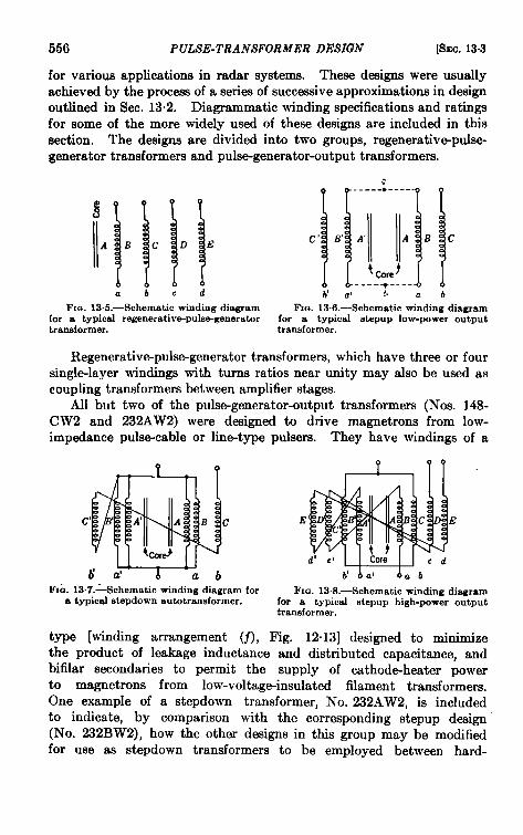
556 PULSE-TRANSFORMER DESIGN [SEC. 13.3
for various applications in radar systems. These designs were usuallyachieved by the process of a series of successive approximations in designoutlined in Sec. 13.2. Diagrammatic winding specifications and ratingsfor some of the more widely used of these designs are included in thissection. The designs are divided into two groups, regenerativ~pulse-generator transformers and pul-generator-output transformers.
“1’1’1”1’ ‘1’[ ‘:lB/ca bcd h’ aI !,ab
FIO. 13.5.—Schematic winding diagram Fm. 13.6.—Schematic winding diagramfor a typical regenerative-pulse-generator for a typical stepup low-power outputtransformer. transformer.
Regenerative-pulse-generator transformers, which have three or four
single-layer windings with turns ratios near unity may also be used as
coupling transformers between amplifier stages.All but two of the pulsegenerator-output transformers (Nos.
CW2 and 232AW2) were designed to drive magnetrons fromimpedance pulse-cable or line-type pulsers. They have windings
c c E E
148-low-of a
FI& 13.7.%chematic winding diagram for FIG. 13.8.—Schematic winding diagram8 typical stepdown autotransformer. for a typical E&pup high-power output
transformer.
type [winding arrangement (f), Fig. 12. 13] designed to minimize
the product of leakage inductance and distributed capacitance, and
bifilar secondaries to permit the supply of cathode-heater power
to magnetrons from low-voltag~insulated filament transformers.
One example of a stepdown transformer, No. ~2AW2, is included
to indicate, by comparison with the corresponding stepup d~ign
(No. 232BW2), how the other designs in this group may be modified
for use as stepdown transformers to be employed between hard-

SEC. 13.3] TYPICAL PULSE-TRANSFORMER DESIGNS 557
tube pulsers and low-impedance cable. All of these transformers, except
No. 148 CW2 and 148 DW2, have values of n between 3 and 5.The values of pulse duration and load impedance given in Table 13.1
for these transformers are, in general, those determined from the values ofshunt inductance, leakage inductance, and distributed capacitance by
. .
FIQ. 13.9.—Some examples of low-power regenerativ~puls~generatir pulse transformers.
the method outlined in Sec. .13.1. The voltages given are determinedfrom insulation thicknesses and from a stress factor of 25o volts per milfor oil-impregnated units, or 100 volts per mil for small dry-type units.
In Figs. 13.5 to 13.8 a single coiled line represents a single windinglayer, which is, in general, to be centered on the coil form. In general
FIO. 13.10.—Three pulse transformers designed for operation at 120 kv, 0.5, 1.0, and2.0 paec. (a) Core-and-coil assembly of an oil-filled pulse transformer (232-BW2) on a0.002-in. Hipersil core. (b) G. E. pulse transformer with Permaill insulation on a O.OWA.Monemax core. (c) Westinghouse pulse transformer with Fosterite insulation on a0.002-in. Hipemil core.
all windings on one leg of the core are wound in the same direction. Inthese figures, however, the windings on one leg are wound in the oppositedirection from the windings on the other leg. Connections between wind.ing layers are indicated by straight lines The wire size and the number

Design
pulse volt-age, kv
pulse dura-tion,Nec
Maximumduty ratic
Load imped.ante,ohms
Noninducedvoltages,volts
32 AW
1/1/1
).3-1.5
0.002
250
1
TARLE 13.1.—OPERATING DATA FOR TYPICAL PULSE TRANSFORMERS
145 CW2
.5/0.5/0. !
1-5
0.002
w
0.5
:24 AW2
/1/1/0.:
D.1-O.5
0.002
1000
1
~48 CW2
i/o.2(a)”2/O.4(b)
2/O.4(c)
), 6-3(a) j0.25-2.5(b)
o.5-2.5(c)
0.002
1600(a)1000(b)2000(C)
. . . . . . .
32 AW:
2.5/2. !
).5-2.5
0.001
50step-down
. . . . . .
2.5/2. !
).5–2.5
0.001
1250
. . . . . .
?32FW2
16,5/3.3
25–1.25
0.001
1250
. . . . . . .
35DW
28/7
1-2
0.0006
400
. . . . . .
111IW2
36/12
1.5-2.5
0.0006
450
. . . . . .
55 BW
15/3 .3
1-5
0.001
1000
. . . . .
77 BW
54/24
1
D.0005
250
. . . . . .
—.10 AW2
22/5.5
).5-2.5
0.001
800
. . . . . . .
● (a), (b), and (c) refer to the voltage rationobtained with the various ways of connecting the transformer.t (a), (b), and (c) refer ti the vari.un pufss dorations that can he obtained at ratad vokase with the variO~ cOnn@tiOmw~ch Sive fie ~ VOl@geratiO @), (b).
sod (c).

SEC.13.3] TYPICAL PULSE-TRANSFORMER DESIGNS 559
of turns are given in Table 13.2. The total thicknesses of the insulatingpads between the winding layers and between the inner winding and thecore are given in roils. Pads between windings that are 15 roils thick orgreater are usually wound with 5-roil unsized Kraft paper; those of lessthickness are wound with 2-roil Kraft paper. A part of the thickness ofthe pads between inner windings and cores may consist of a fiber coilform; this form should fit closely around the core in order to make themean perimeter of the coil a minimum. Vacuum (less than 1 mm ofmercury) impregnation with a good grade of transformer oil is recom-mended for all units rated at greater than 6 kv. Any of the varnishes of
FIG. 13.1 I.—Threepulsetransformersdesignedfor operationat dMerentpowerlevels.(a) 120 kw (232BW2) with weUfor magnetron(Westinghouse). (b) 2 Mw (GE) (.)10 Mw (377 BW2) with form-fitting weU for magnetron (GE).
the solventlem type, which harden without leaving voids, may be usedfor the dry-type units (which are rated at less than 6 kv). Good solvent-type varnishes may also be used for units rated at less than 2 kv. Startd-ard sizes of Westinghouse 0.002-ii. oriented Hipersil cores are specifiedthroughout, except in some cases where two standard loops maybe placedside by side to make up the specified strip width.
Figure 13.9 shows several examples of low-power regenerative-pulsegenerator transformers that have been developed; Fig. 13-10 shows three120-kw pulse transformers; and Fig. 13.11 shows three pulse transformersof pulse powers of 120 kw, 2 Mw, and Id Mw. Two of these latter trans-formers have wells into which the magnetron may be plugged. The wellof the 10-Mw transformer is form-fitting and is greased with Dow-Corning Compound to exclude air when the magnetron is plugged in.Figure 13.12 shows pulse transformers employing permalloy cores and

560 PULSE-TRANSFORMER DESIGN [SEC.13.3
(a)
(b)
Fm. 13.12.—Three pulse transformers constructed with continuously wound permalloycores (Western Electric Company). (a) Rectangular core of l-roil 4-79 molybdenumpermalloy and pulse transformer in which it is used. Pulse power: 100 kw. (b) 3-lb.rectangular core of 2-mif 46 permalloy and ~-lb. core of l-roil 4-79 molybdenum permalloywith the pulse transformers in which they me used.

TABLE13.2.—DEEIQNSPECIFrCATIONSFOR TYPICAL PUME TRANSFORMERS
=7== ==I==Design 132 AW2 145 CW2
~ore window, in.: 1X*8tn , in.
— ~
B~d, in. A L
224 AW2 148 CW2
1X*
L
232 FW2 285 DW2 311 1W2
351+
1*
Fig. 13.8Cg;
21-#233 in //
410 Aw2
}Xi#
-iqr —lip+
h *imii — Figti;38
o. :2! 0.02025-#26
] I
2Ć in // 2 in //
0.050 050-+26
247H
i
Fig. 13.8
0!0!526-L9222 in //
*FigH~3%
0.02514-f232 in //
-Fig. 13.80,$$
16-1213 in //
Assembly wire Fig. 13.5 Fig. 13.5
A, in. 0.015 0.020a { 32-#2o 125-{36
B, in. ~ — 0.005b { 32-#30 125-#36
Fig. 13.5
0.02035-#22
0.0103&jti2
:,%2’62&33
0,02011O-N5
0.01016-#213 in //
0.01021-#233 in //
0.005JI
o34-#23
o 0.01026-*222in //
0.07539-#19
TGii- — 0.1s06%+27
1
10-+238 in //Tt
c — o6&t27
c, in. 0.010 0.005c { 32-#30 12c%#26
D,in. — niGi-d
0.015
{
0.01035-#32
0,0101O-*21
0.020
. . . . . . . .
0.050 0.040W +26
— =Ga--. . . . . . . 50-+26
0.1002S-{23
0.0052S-#23
0.08024-+212 in //
0.01024-.#2l2 in 11
O.ow21-+233in //
0.01021-#233 in //
o 01039-#19
0.050E, in. ,. . . . . .A’, ina’ F T
0,020 I 0.050 0.050 0.070 0.090. . . .0.02022-t355 in //
0.0201lo-t25
0.020. . . . . . . .
0.025 0.0202S{26 25+262in //
] }
2 in //
0.030 050-126
0.02514?232in //
0.050l&f213 in //
0.01016-#213 in //
O.ow21-#233 in //
0.01021-#233 in //
0.030 0.20034-#23
}
16-#235 in //f
c — o34-!23
0.04526-#222 in //
0.01026-+222in //
.. .. . . . .-
0B’, in.b’ [........ . . . . . . . .
c, in.1? F -
.. . .. . . .
—-i7G-0,040. . . . . . . . 50-+26
0.05023-+22
0.0052s-+23
0.01024-{212 in //
0.010
%+Y/
0.04521-#233 in //
0.01021-#233 in //
0.025 O.lw60-*27
I
10-#238 in //tt
= — o6Ck+27
0.04039-#19
0.01039-L?19
. .. . . . .
— 7GF. . . . . . . . 50-+26
D’, in.# l{........ I....... .. .. .. . . . .. .. .. .
— —, ~. .. . . . .. . . . . .‘ /3
Ih h PrilUW,2 in .wmmdsry,
t 3 cottin 00r& sQu.din diameter to
.. . . . . . I 0.040 ~ 0.030 0.054) 0.050 0.040 I 0.120 0.040... ...,.Cordm
. .. . . . .Parallel.
F undmple formsx.%F eavy formex.
MO means 32 tum of No. 30 wire.
m wire.,wound in pamlkd with the wirs ta effemtnpace-winding.

562 PULSE-TRANSFORMER DESIGN [SEC. 13.3
constructed with diaphragms to accommodate the thermal expansion ofthe oil.
In these figures are exhibited some of the final results of the designer’seffort.
Swmrzu~.-Chapter 13 has established relationships between theelements in the equivalent circuit of the pulse transformer and theoptimum load impedance, pulse duration, and efficiency. General designmethods for achieving these relationships in building the pulse tran~former have been advanced, and two examples of the application of thesemethods are given. The design data on a number of successful pulsetransformers are given, and methods for employing these data and thegeneral design methods used in deeigning new transformers are outlined.

CHAPTER 14
‘i.
EFFECT OF PULSE-TRANSFORMER PAM.METERSON CIRCUIT BEHAVIOR
BY W. H. BOSTICK
14.1. The Effect of Pulse-transformer Parameters on Pulse Shapeson Resistance and Biased-diode or Magnetron Loads.—This sectiontreats in turn, the effect of the pulse transformer upon the rise, the top,and the tail of rectangular pulses applied to the primary when resistanceand biased-diode loads are comected to the secondary. In this treat-
FIG. 14.1.—Equiv”alentcircuit of a pulse generator,a P~se transformer, and aresistance load.
L,,
a mT
~EIll
RC c R, e,
-=+- K
FIG. 14.2.—Equivalent cir-cuit for the computation of theris of the pulse on a resistanceload.
ment the simple equivalent circuit of Fig. 14-1 k, for the most part,employed, and the rectangular pulses are considered to be generated bythe closing and opening of the switch shown in the circuit.
The Rise of the Pulse on a Resistance Load.-The rise of the pulse on aresistance load RI is considered for a transformer in which the effect ofR. is assumed to be negligible compa -d with that of Rl, and where thetime of rise is so short that the effect of L. is also negligible. The initialenergies in LL, L., and C are assumed to be zero. The mesh currentsmay be chosen as shown in Fig. 14”2, The Laplace transforms of themesh equations may be written as follows:
( )~ L(p) –*Ci2(P) = ~P2+g P+LLcv.
( 1)”— *c L(P) + P + ~c ~2(P) = 0,
56a

564 PULSE-TRANSFORMER PARAMETERS [SEC. 14.1
whence
e(p) = R&(p) = ~+c[( ‘“ ‘)i’+w=l
P2+~LP+LLc
‘“p[p2+(g+*jp+*(1+g)];=mor
1Rriz(P) = #C ~(pz + 2ap + b)”
Then
‘(’)‘#%J1-e-’fsin’k’+co’hk’)l’ “)where
andl#=a2–h.
when
b > af,
k = ju,
&= b-a2,
and
a(’)‘*l[l-e-’(:sin@’+ cOs@’)lo ‘2)To show how the rise of the pulse is affected by variation in the values ofthe elements in the equivalent circuit of Fig. 14.2,
<bis plotted in Fig. 14.3 against T = ~ t for different values of the param-
eter u, where tCRJL + L.
u - a = 2 <RILLC(R. + i?,)
If R. ia so small that RO << Rl and CR. << LL/Rl, as it is in a hard-tubepulse generator, and if OC is made equal to RI, as has hitherto beenfound advisable, c = 0.5. If Ra = Rl, as itdoes in a line-type pul~

SEC.14.1] EFFECT ON PULSE SHAPES 565
generator, and if ~ is made equal to Rz, u = I/w = 0.71. Fromthe curves of Fig. 14.3 it may be seen that these two values of u givereasonably good compromises between maximum rate of rise and mini-mum overshoot.
Rise of the Pulse on a Magnetron or a Biased-diode Load.-The rise ofthe puke on a magnetron or biaseddiode load is considered for a trans-former in which the effect of R. is negligible compared with that of Ra,
and where the time of rise is so short that the efiect of L. is also negligible.
20
M
1.6
1.4
— 12Cqrr
=
0.6
0.4
02
: 1.0! I I Il#j x 71I )/
+-. 0.8H-1
0.2 0.3 0.4 05 0.6 0.7 0.8 0.9 MT= ~. *
F’”’’”’-”’”f%(l(l +%) “T ‘~’
Both a magnetron and a biased-grid load exhibit the general load charac-teristics of a biased diode, which is represented in the equivalent circuitof Fig. 14.4 by a battery, series resistance, and switch that closes when thevoltage acroes the load is equal to or greater than the battery voltage.
If mvitoh 1 closes at t = O and switch 2 is open,
and e!(t) can be obtained from Fig. 14.3 by choosing a curve correspondingto a value of u obtained by letting Rl = ~ and RQ = O for the hard-tube
pulse generator, or Iik = -C for the line-type puke generator.

566 PULSE-TRANSFORMER PARAMETERS [SEC. 14°1
Although the energy stored in L. (see Fig. 12.7) has some effect uponthe shape of the current and voltage pulses in the load, it is neglected thusf:lr in this computation for two reasons. First, the introduction of L~
in the equivalent circuit represents only approximately the actual condi-tions existing in a transformer; and second, it is desirable to keep the setof assumptions for the design of a transformer simple, and thus to includeonly the most important circuit elements. For these reasons also, L.
is neglected in the treatment of pulse-transformer design in Sees. 13.1and 13.2, and later in this section the effect of L~ on pulse shape is treatedas a second-order effect.
It is desired, to a first order of approximation, to design the trans-former so that the current flowing in LL and into C at the time tl when
FIG.14.4.—Ci rcuitfor the computation ofthe rise of a pulse on abiased-diode load.
switch 2 closes is equal to the current that theload will eventually pass when there are effectivelyonly the two batteries and two resistances in series.There will then be no high “spike,” or excessiverounding-off of the front edge of the current pulsein the load.
The first type of pulser operation that is dis-cussed is that of a biased-diode load and pulsetransformer with a hard-tube pulse generator,where usually i lR~ << Vo, izRO << V~, and izrl << V.
(see Fig. 14.4). The pulse generator is usuallydesigned so that VQ = V. = the desired voltage on the load. Since Ro
is small, Eq. (3) may be written
v. .ii(t)= —
& r~t.L. ‘ln LX
c
It may be seen from Fig. 14”3 that, for the curve u = O (that is, forRQ=O, Rl = m),
1+.= ‘%
at the moment when
“d
T.‘ln Ec t = ‘ln J_
L+c tl = 1.
At this moment
and if -C is chosen to be equal to Rl, the static impedance of the
SEC. 14.1] EFFECT ON PULSE SHAPES 567
load at the point at which the tube is to be operated, il has the propervalue at the time t, when switch 2 closes. Immediately after the timetl there is a very brief interval of time during which a small additionalrise in el requires some of the current which is flowing in Lt. to flow into C.Forthe remainder of thepulse, however, el remainsat a practically con-stant value, and all the current flowing in LL flows through the load rl.
The value of i, as a function of t, reckoned from the time of the closingof the switch 2, is
(ii(t) = io– V@;:)e-(%p),+ ~G-: ~,,(,,,
where iOis the initial current in LL at the closing of switch 2. If
io is too large, and there is exhibited on the front edge of the current pulsea spike that decays to the equilibrium value of the current with a timeconstant approximately equal to L./ (RG + rz).
If -C > RI, io is too small, and the current pulse has an initialvalue that is too low. The equilibrium value of the current pulse isapproached with the same time constant approximately equal to
L.
(RG + r,)”
There are, of course, oscillations on the current pulse. These oscil-lations, to a first order of approximation, may be said to be caused bythe shock excitation of the L~C~-branch of the equivalent circuit of Fig.12.7. They are, in most cases, of a period shorter than the time con-stant LL/(RG + n) and are superimposed upon the general trends thatoccur with this time constant.
The observed rise of current pulses on a magnetron and calculationsaccording to the foregoing assumptions are in good agreement (see, forexample, Figs. 2.44 and 2.45).
The second operation to be discussed is that of a biased-diode loadand pulse transformer with a line-type pulse generator, where usuallyv. = 2v,, RG = R1 (after the closing of switch 2), and Ra >> rl (when allvalues are referred to the same impedance level). Prior to the closingof switch 2 in Fig. 144 it is assumed that RI is infinite. Then, if
~ = 0.50 and

568 PULSE-TRANSFORMER PARAMETERS [SEC, 14.1
Eq. (3) then becomes
v. r— e-~ sin 0.866 ~+ t.~l(t)= o.8&3&
and
In Fig. 14.3, for the curve corresponding to u = 0.5,
()1 v*;.=5 = T.
at T = 0.207.
ThenRot
e–z = ~–0.207.r = e-0.660 = OJZ.
Also,
sin 0.866c
~ t= sin 0.866. 2X .0.207 = sin 65° = 0.903,LLC
Thus. _ V. 0.52.0.903 v. v. v.
21 – K. 0.866 ‘“”hrm=--” R. i- Ri
Thus, in a linetype pulser, if ~C = Ri, the current flowing in LL’
at the time when switch 2 closes is equal, to a reasonable approximation,to the equilibrium current (that is, the current that flows when Vu,
V,, Ro, and rl are connected in a series circuit). If -C # R,, the
m
Tsame exponential approach to the equilibrium@@ value of the load current occurs, but in this case
Ro the time constant LL/(RQ + n) is much shorter.LP R, e,
1
The Top of the Pulse on a Resistance Load.
-= VG The beginning of the top of the pulse on a resist-+ ante load is influenced by LL and C, as may be
seen from Fig. 14.3. There is also a droop in theFw. 14.5.—Equivalent
circuit for computingthe pulse when RG >0, because of the fact that cur-
droop on the top of the rent builds up in L,. Since the effects of L. andPulseon a resistanceload. C. usuallyare relatively unimportant as far asthis droop is concerned, the equivalent circuit of Fig. 14”5 maybe used inthe computation of this droop. The initial current in Lp is assumed to bezero, and tis reckoned from the beginning of the top of the pulse. Then
1 RoR,v~, -–.—
‘i(t) = R= + &e & Ru+RJ*.

SEC. 14.11 EFFECT ON PULSE SHAPES
When, as in most line-type pulse generators, R. = RI,
569
The TOD of the Pulse on a Magnetron Or a Biased-diode Load.—The
beginning ~f the top of the pulse on a magnetronor biased-diode load has oscillations which, asalready shown, may be considered to be caused bythe shock excitation of the LDCD-circuit in Fig.12,6, and may also have a spike or an upward slope
depending upon the value of -C relative toR1. When R. >0, there is a general droop onthe pulse, and this droop may be calculatedapproximately from a consideration of the equivwlent circuit of Fig. 14.6, whence
FIG, 14.6.—Equiva-lent circuit for cOmput-ing the droop of thecurrent pulse on a biased-diode load.
[(v. – v.iz(t)=
R. + T1 )+ : ~-+”~~ _ ~
?-I1and
el = V, + iZrt.
(When el becomes equal to or less than V,, the L-branch of the circuit
I IIti t~t~
FIG. 14.7.—Typical pulse and backswingproduced by a pulse transformer.
voltage oscillations produce current
must, of course, be considered tobe open-circuited and the aboveexpression for iZ does not holdthereafter.)
Thus the top of the currentpulse iz on a biased-diode loadsuffers much more droop than thetop of the corresponding voltagepulse, or than the top of the pulseon a resistance load. For thesame reason any voltage oscilla-tions caused by the transformerproduce much larger fluctuationsin the current pulse because these
flow through the relatively smallresistance TZ instead of through the higher resistance R1. Calculationsand measurements of the droop of the pulse on resistance and magnetronloads agree withh-z the experimental error.
Gerwral Backsun”ng on the Tail of the Pulse. —Figure 14.7 shows a pulsewith the characteristic backswing produced by the pulse transformer.

r
570 PULSE-TRANSFORMER PARAMETERS [SEC. 141
Since the flux density must return to the same remanent point B, beforethe beginning of each pulse [see Fig. 152 and Eq. (15.10)],
/
h
\
–NA ‘-dB = –NA -area (1) = eLdt=—
0 108 B,,T ‘Bwx - ‘r)’
and
/
t4area (2) =
/
–NA “ ~B = –NA_—‘t ‘t – 10s ~_
~ (B, – ~w),t,
area (2) = – area (1). The interval of time tA– h is chosen to be solarge that, for all practical purposes, e~has become equal to zero. Thus,when a pulse transformer is used, there is always a general voltage back-swing whose area is equal to that of the pulse itself, but whose shape isdetermined by the values of R., C, L., and R, if a resistance load is stillconnected, and by the charge on C and the current in L= at tz. When Rl
becomes infinite, at a time very shortly after h,
m
Tthere are oscillations of a higher frequency super-imposed upon the general backswing because of
L@C; R ec energy stored in LL.
1
The shape of the general backswing may becalculated by assuming that the constant-voltage
Fm. 14.S.—Equiva- generator V~ is disconnected from the circuit atlent for the computation the time tz (see Fig. 147). The equivalent circuitof the pulse tail. is then that of Fig. 14.8 where, to a goodapproximation, the initial current in L, is Vih/L. and the initial voltageon C is V1.
Then, if t = O at the time tz,
( #c+acc(t) = VZ e-~ cosh let– e ~
)sinh Id
for the nonoscillatory condition, and
( +C+acc(t) = VZe_’~ cos d — ‘ ~
)sin d
for the oscillatory condition, where
I
andk = –ja.

SEC. 14-1] EFFECT ON PULSE SHAPES 571
When a pulse transformer is used on a resistance load, R = Rl, andthe pulse tail is usuafly “well dampd” (see Fig. 14”9). When a pulsetransformer is used on a biased-diode or magnetron load, the load isdisconnected very shortly after tzand R is essentially equal to R, (if noartificial diode or resistance damping is used in the circuit). A typicalbackswing (without the superim-posed oscillations) for this latter caseis also shown in Fig. 14.9.
When a pulse transformer is usedwith a lin+type pulse generator, theeffective value of C in Fig. 14”8 isequal to the sum of the distributedcapacitance of the pulse transformerand the capacitance of the load.When a hard-tube pulse generator isemployed with stepdown and stepuptransformers. the effective values of
*’t]~
FIG. 14.9.—Typical backswings withresistance and bksed-diode loads.
R and L are respectively eaual toRJ2 and L.;2, and the effective value of C is equal ~o the ~um”of theeffective distributed capacitance of the two transformers, the load, andthe pulse generator. Calculations and measurements of the generalshape of the tail of the pulse obtained with hard-tube and lin~type pulsersemploying pulse transformers and either resistance or magnetron loadsagree within the experimental error.
LL LL
— f~~ L
‘ha
~Re >= CG+CD C,+ CD== Re 2
\
Tc-Re,
&:=
1FIG. 14. 10.—Equivalent circuit for the FIG. 14.11 .—Circuit
computation of oscillations appearing on the approximately equiva-pulse tail with a hard-tube pulse generator lent to the circuit ofand a biased-diode load. Fig. 14.10.
Oscillations on the Pulse Tail.—The tail of the voltage pulse from atransformer on a resistance load usually exhibits no oscillations super-imposed on the general backswing (that is, the energy stored in LL hasvery little influence on the voltage-pulse tail).
However, on a biased-diode or magnetron load, oscillations usuallyappear which are superimposed on the general voltage backswing. Inthe analysis of these oscillations the example of the hard-tube pulsegenerator with two pulse transformers, the effective equivalent circuit

572 PULSE-TRANSFORMER PARAMETERS [SEC. 14.1
of which is shown in Fig. 14.10, is considered first. The load current 11flowing in L. at the end of the pulse is suddenly interrupted by the open-ing of switch 2, and the pulsegenerator voltage source has been dis-comected. To a good approximation, the circuit of Fig. 14.10 may bereplaced by that of Fig. 14.11, where
L = 2L.,
1 1 1V=c. +c. ‘cD+ Cl’
R = 2R..
The initial current in L is 11, and, for the purpose of calculating the oscil-lations occurring on the backswing, the effective initialzero. The voltage c1is then given by
charge on C is
If, as is usually the case,
()12&>> —
2RC ‘
then
These high-frequency oscillations are superimposed upon the generalbackswing to produce a pulse tail such as is shown in Fig. 1412a. If a
fu
/I
(a) With a hard-tube pulse generator. (b) With a line-type pulse generator.FIG.14. 12.—Typical voltage-pulse tails on a magnetron load.
cable is used between the stepdown-stepup pulse transformers, the period
of oscillation 27r-C is increased by twice the transit time of the cable.There is good agreement between the calculated and the observed
pulse tails obtained with a hard-tube pulser, pulse transformers, andmagnetron load.

SEc. 14.1] EFFECT ON PULSE SHAPES 573
In a line-type pulse generator with a magnetron load there is a mis-match in impedance at the magnetron when the pulse voltage drops atthe end of the pulse. As a result, a small portion of the energy is left inthe circllit in the form of a negati ve voltage spike that is propagated downthe pulse-forming network, reflected at the open end, and propagatedback to the pulse transformer, where it appears as a negative spike on
n ~(a) R,; = O, r = ~out,ZT = R,
y = o, 0,05,0.1, 0.2, 0.3@) R~ = R,, r = Top,, Z~ = Rt
y = o, 0.05, 0.1, 0.2, 0.3
(c) R,; = O, ZT = RI, T = o.1T = :, 1, ‘2T.pt
(e) m =0,7 =T.,,, -y =0,1.Z~ = ~, 1, 2RL
(d) Rc; = R{, ZT = R/, Y = 0.1T = +, 1, 270Dt
(-f) Ro = R[, 7 = rope, 7 = 0.1ZT = ;, 1, 2RI.
I~Iu, 14.13. –Pul,c Sh:LpCS on a rcsistsmce load co>ultitcd for various values of the
dLr, T
~,L1’Ul,,.t,l’S. (a + B)oP, = ~; ~ = ~j CD, ~z~~= r .Ro.
ro~t ‘ Rt
the tail of the voltage pulse. Such a series of spikes, drawn from a syn-
chroscope trace obtained with a line-type pulse generator having a rotaryspark gap as the s~~itch, is sho!vn in Fig. 14. 12b.
The General Pulse Shape on a Resistance Load. —With the assumptionof a resistance load hai’ing no appreciable capacitance, the effect on pulseshape of varying the values of the parameters

574 PULSE-TRANSFORMER PARA METERS [SEC,14.1
(a + L% = 7,
and Ro/Rl is calculated on the basis of the equivalent circuit of Fig. 13”1,and is shown in Fig. 14.13. For increasing values of y, as shown in Fig.14. 13a and b, the approximations used in formulating the simplifiedequivalent circuit of Fig. 13.1 become greater, and hence the error in thecalculated pulse shapes becomes greater.
Current Transformms.-A pulse transformer is sometimes used withits primary in series with a load in such a way that the load current passesthrough the transformer primary. A transformer of this type has been
Outputpulsetransformer
“qJF ‘:K–
FrQ.
Currenttransformer(a) (b)
14. 14.—(cz) A typical circuit using a current transformer. (b) Circuit equivalent to (a).
termed a ‘‘ current transformer” although the transformer actuallytransforms power, as do all transformers. Such transformers are oftenused in the generation of trigger pulses of about 100 volts, and a typicalcircuit is shown in Fig. 14.14a.
The equivalent circuit for the current transformer and the associatedcircuit is given in Fig. 14. 14b, where the stepup pulse transformer withmagnetron load is replaced by a resistance Rt = 50 ohms. All quantitiesare referred to the primary of the current transformer.
If L, is sufficiently large to be neglected in comparison with R/nz,
and if the effects of LL and C’Dmay be neglected, the voltage V dividesbetween Rt and R/n’ in such a way that the voltage across the primaryof the current transformer is
The voltage across the secondary of the current transformer is thenVR/Rm. It is thus seen that, for a given value of R, the voltage across

SEC. 14.2] EFFECT ON REGENER.4TIVE PULSERS 575
the secondary of the current transformer increases if n is decreased, pro-vided that the current in L= remains small compared with that in R/nz.
Obviously, it is desirable to have only a small fraction of V acrossthe primary of the current transformer, and it is therefore desirable tochoose values of R and n such that the proper output voltage is obtained,parasitic oscillations (from L. and CD) are sufficiently damped, and asufficiently small voltage is applied at the primary.
Current transformers of this type may be used to view the currentpulse in a magnetron or other load. Under these circumstances the“ primary winding” may be the lead (or leads) carrying the load current,and in most instances this lead need only be passed through thecore window to produce sufficient output voltage at the secondaryterminals.
14.2. The Effect of Pulse-transformer Parameters on the Behaviorof Regenerative Pulse Generators.—The general criteria of Eqs. (13.4),(13.5), and (13.6) hold for regenermtive-pulse-g en e r a t o r (blocking-oscillator) transformers as they dofor most pulse transformers. Thus,for a regenerative-pulse-generatortransformer the optimum pulseduration is equal to ~~~, andthe excellence of the transformer is
judged by the value of (a + 13)~P,.For a regenerative pulse generatorthat supplies no appreciable powerto an external circuit, the second-ary-winding impedance v’~~should be chosen approximatelyequal to the effective impedance ofTO(the grid-to-cathode resistance)
‘ATobiassupplyEm if triggeristo k usedexclusively.or to
groundif“selfbias” is ~obe used(eitherwithor withouttrigger)
F1~.14. 15.—Circuit of a typical regenera-tive pulse generator.
and C in-series, or of T@and the impedance of the line in series if a lumped-parameter line is used instead of C’ (see Fig. 14.15).
There are several variations on the general scheme of regenerativepulse generators or blocking oscillators. These circuits, however, areall essentially the same in their mode of operation, and a general physicaldescription of their operating mechanism is given in Sec. 4.2. As anexample of a regenerative pulse generator, the circuit shown in Fig.14.15 is used to show the effect of pulse-transformer parameters on circuitbehavior. The voltage stepup ratio of the pulse transformer in thisexample is chosen, for purposes of simplification, to be n = —1, that is,the windings of the transformer, although wound in the same direction,are connected so that the pulse to the grid is inverted. It may prove

576 PULSE-TRANSFORMER PARAMETERS [SEC. 142
advantageous in practice to select different values of n for different tubeand load characteristics.
There are various stray capacitances in this circuit and the pulsetransformer has a certain amount of leakage inductance; in order to avoidthe difficulties involved in the analysis of such a complicated circuit, it isprofitable to start first with the most simplified of equivalent circuits andthen to proceed to the more complicated circuits that take into considera-tion more of the actual circuit elements. The analysis of the pulse-mak-ing operation is treated by considering first the leading edge or rise ofthe pulse, second the top of the pulse, and third the tail of the pulse.
In order that linear analysis may be employed, the plate resistance rfland amplification factor M of the tube are considered constant for theperiod of time under immediate consideration.
FIG. 14. 16.—Simplified equiva- FIe-.14.17.—Ckcuitof Fig.lentcircuitfor a regenerative pulse 14.16 further simplified bygenerator in which the effects of setting ea’ = leg — Z..C, COP,r=,L= (and ,Z.L)are neglected.
The Rise of the Pulse.—For purposes of simplification, it is assumed inthe beginning that the effect of the trigger circuit is negligible, that r, = (),that the effect of the leakage inductance is negligible in comparison withthat of R, that C = O (see Fig. 14.15), and that the plate-to-grid capaci-tance Co, of the tube is negligible. The equivalent circuit is then that ofFig. 1416, where C’~ and LL are, respectively, the effective distributedcapacitance and leakage inductance of the transformer. It is assumedthat the bias voltage
E,= Em+e,
where ~ is a positive voltage which can be vanishlngly small, but which,nevertheless, can instigate the process of regeneration. It is readilyshown that this circuit can be simplified to that of Fig. 14.17, wheree; = leg – Eal.
Kirchhoff’s voltage-law equation for the circuit yields the followingdifferential equation, where the initial voltage on c. is equal to zero:

SEC. 142] EFFECT ON REGENERATIVE PULSERS
The Laplam transform of this equation is
577
(z+++’’=’~(’’+t=%‘since
and therefore
Then
The change in plate voltage on the tube is givenrP has been assumed to be equal to zero. Then
u—l—
t?b =~e(efiRt — 1)
p–l “
by eb = —pe~, since
(4)
If p is greater than one, the exponent is positive and ~generationtakes place in such a way that Ieblincreases until lebl= Ebb. Throughoutthis section it is assumed that when the generator output voltage (whkhin this example is – eb) is equal to Ew, the amplification factor p of thetube is less than one, and that regeneration therefore stops. If it isassumed that, during the rise of the pulse until the generator outputequals Ebb, the average value of P is given by p[E~l = Ew, p must beassumed to become suddenly less than 1 at the moment when e; becomesequal to or greater’ than lE~l. The voltage e, pawws through zero andgrid-to-cathode current begins to flow at this moment. Although theequivalent circuit must be modified at this instant to account for thegrid-t~cathode current, this modification can be made with relative easebecause the generator output attains its peak value Ebb at this momentand remains constant as long as e~ > 0. For purposes of simplifyingthe analysis the assumption that y = lEbb/Eml is, therefore, uced through-out this treatment of the regenerative pulse generator. This simplifica-tion is desirable because the aim of this treatment is to show analytically,rather than numerically, how the elements in the equivalent circuit of apulse transformer affect the puke shape produced by a regenerative pulsegenerator.
Perhaps a more appropriate assumption with regard to the averagevalue of p during the rise of the pulse is to let
/41&ol+ ~) = EM,

578 PULSE-TRANSFORMER PARAMETERS [SEC. 14.2
where e: is a positive grid voltage at which P begins to change abruptlyfrom a value greater than one to a value much less than one (see Fig.14.26). In computing the rise of the pulse under this assumption it isnecessary to make the circuit modification (with appropriate boundaryconditions) at the moment e~ passes through zero whale the generatoroutput is stii rising. It is assumed that the generator output continuesto rise until eu = efl, at which time p is assumed to become <<1, and thegenerator voltage is assumed to remain constant at EM as long as e, z e;.A linear solution of the rise of the pulse under these circumstances couldalmost never be given in an analytical form, and therefore is of littlegeneral value to the puke-transformer designer.
If, in the simple example under consideration, it is now assumed thatthe leakage inductance L. is finite, LL may be inserted in series betweenthe generator and CDin Fig. 14.17. The Laplam transform of Kirchhoff’svolt age-law equation for this circuit then becomes
(LLP + c~p)
pi(p) + :,L+ Ri(P)=m p
whenoe
ei(p) =
[ (–)11 l–/.I ‘LL P’+~Lp+~L C.
ej (p) =
[LL13DP P + & – [w-k]”) “
[‘+*+[H -=1%1The change in “plate voltage on the tube is again given by eb = – pe~,since rPhas been assumed to be equal to zero. The solution is of the form
f?b(p) =(P+ a)7P + 7)P’
(5)
whose inversk Laplace transform is
where
(6)
a“ = L.%D’
a=%- [(war)

EFFECT ON REGENERATIVE PULSERS
‘=&+ [(&Y-sl” “
“=%-[(+)%%1)””,that is, if p > 1, the first exponential term contains a positive exponen-
SEC. 14.2]
and
579
If
tial, and regeneration occurs.The solution (6) may be put in the following form:
- ‘-wsinh[(a%w
/.lc_ ,_:[(&Y-%l%’osh [(*)-21’”1‘p–l
1[(a%]% “If p is large enough and R small enough to make
/.L-l
–()
R’
LLCD >>Z’
a = —~, and Eq. (6) becomes
‘b(’)‘+ -Coshw’l
(7)
(8)
The output lebl of the generator in Fig. 14.17 continues to increaseaccording to the expression given in Eq. (7) [or that in Eq. (8), if the
Rflall . .FIG.14 lS.—Equivalent circuit for a regenerative pulse generator where the effect of
R and COPmay be neglected. (a) Initial voltage on C’equalto ECO+ c. (b) Initial voltageon C equal to e.
approximation is valid] until Iebl = EM, at which time p is assumed tobecome suddenly much less than one and the voltage Ie,l levels off, therebyforming the top of the pulse.
580 PULSE-TRANSFORMER PARAMETERS [SEC. 14.2
The next example to be considered is one where C # O and R is solarge that its effect is negligible compared with that of C, and where theeffect of rP is taken into account. The equivalent circuit is then that ofFig. 14.18a, which can be replaced by that of Fig. 14. 18b for which
Then
A(p) =
‘4P’+:PA+%)I.
[LLCDP P + ~~- [W-:(:+%’)]”} “
(p+*+ [(&+( :+al”lThis equation and its inverse Laplace transform are of the same form,
respectively, as Eqs. (5) and (6), where now
-- [(2)%:+%31’”a=z.and
‘=~+[(a)-+(++%’)l””
The condition for the existence of regeneration is that
:+ +0,or
In the present example ‘b = – pe~ + ir~,whenw
‘b(p) = – y’j (p) + ‘Pi(p)ao
= p(p + a)(p + 7)+ (P+ a%+7)’where
rpeal = ~L’

SEC. 14.2] EFFECT ON REGENERATIVE PULSERS 581
and the inverse Laplace transform of the second tirm is
The complete solution for this example is then
There are two special cases of this general solution that are of interest:
Case 1. Where the time constant a is determined primarily by T=
and Co (that is, LL is negligibly small as far as its effect on i is concerned).For this case the Laplace transform of Kirchhoff’s voltage-law equation is
[(~+a;+”h=%+;whence
and.
4(P) = T2~D‘[’+i+wcc [, -,-M+%)],
ej(t) = CD + L’(1 – p)
and
Case 2. Where the time constant a is determined primarily by ~.and CD (that is, rP is negligibly small as far as its effect upon i is con-cerned). In this case a = – ~ and Eq. (9) may be simplified to give
(=c L(p -“:-cl){’-’”’h[-l!l(:+%)l’”}+ ?-p(fJ/,cD)fi
LL [m-:) --J{ ‘inh[-+(:+%w))(11)

582 PULSE-TRANSFORMER PARAMETERS [SEC. 14.2
If C>> CD and ir, << Ipejl, Eq. (11) can be further simplified tobecome Eq. (8).
From the expression for ebin Eq. (8) it is possible to make a calculationof the time of rise of the pulse when this time of rise is governed only bythe transformer characteristics. Effects that am due to 7P, C, and thegnd-to-plate capacitance COP, of course, actually increase this time of rise.
If it is assumed that c is 1 volt at t = O and if the interval of time,h > ~ >0 elapsing until eb is – 1 volt is computid,
-, =+ -cosh(fi)’tl],
()
%cosh ~
L~C~t, = 2,
or
and if(–)P
H
L.C.t, = 1.32,
(–)
>5
L$D
is known, tl may be computed. If tz > t > 0 is the interval of time.
untd f?b= -10 volts,
() $5cosh ~
LLCDtz = 11,
or
If t~ > t >0 is the interval of time until e, = –3OO volts,
()5$
cosh —L.PCD
ts = 301
and
(–)%LL~Dta = 7.2.
A reasonable definition for the time of rise of a pulse from rtregenera-tive pulse generator would be t3 – tz = At; then

SEC. 14.2] EFFECT ON REGENERATIVE PULSERS 583
For a numerical example, when L. = 20 X 10–6 henry, CD = 20 X 10–’2farad, and p = 20,
At =4.1
( )
)5 = 0.018 @3C.20
20.20 x 10⁻¹⁸
A simple example is now considered where the effect of a trigger circuitof source voltage V~ and internal resistanw r; (see Fig. 14.15) are takeninto account, where the effects of C~~,R,and rn are neglected, and where C isfinite. The equivalent circuit for this ‘~nti,example is given in Fig. 14.19 where the
L~
cinitial charges on C and CD are assumed -to be equal to zero. This assumption is *
G e;equivalent to the hypothesis that the + LLinitial voltage on C is actually Em when 1 =the generator o u t p u t is equal to FIG. 14. 19.—Equivalent circuit
~(eo — Zlm) and the voltage across CD is for a regenerative pulse generator
q,. It is assumed that the couplingwheretheeffectof thetriggercircuitis takeninto accountand wherethe
capacitance between the trigger circuit effectsof Cop,R andrz areneglected.
and the rest of the circuit is so large that its effect is negligible. TheLaplace transforms of the two mesh equations are then
[“++(++%-+’,(” -*’2(”‘0}and
()– +C ~1(’) + #c + P i2(p) = ;.
Then
or
‘l(P)‘ [“++($-%?;[’++1 -A ’12)
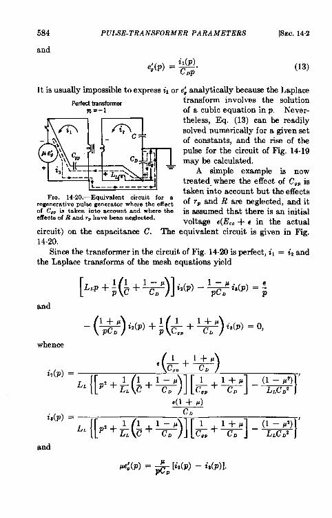
584
and
PULSE-TRANSFORMER PARAMETERS [SEC. 14.2
ii(p)ej(p) = ~. (13)
It is usually impossible to express ~1 ore; analytically because the Laplace
Perfecttransformern=-1
+
L—__* _____
FIG. 14.20.—Equivalent circuit for aregenerative pulse generator where the effectof COP is taken into account and where theeffects of R and rp have hem neglected.
transform involves the solutionof a cubic equation in p. Never-theless, Eq. (13) can be readilysolved numerically for a given setof constants, and the rise of thepulse for the circuit of Fig. 14.19may be calculated.
A simple example is nowtreated- where the effect of C.P istaken into account but the effectsof TPand R are neglected, and it
is asaumed that there is an initialvoltage ~(E,o + c in the actual
circuit) on the capacitance C. The equivalent ‘circuit is given in Fig.14.20.
Since the transformer in the circuit of Fig. 14.20 is perfect, il = iz andthe Laplace transforms of the mesh equations yield
[L’P+;(*+%)I’’(P) -*’’(P) ‘:and
-(*)i2(p)+i(&+*) i$’”) ‘“J
whence
(~+~i2(p) =
)
“h’+w+$)lk+%l - ‘La’6(1 + /L)
L(p) =
‘d[p’+w+w)!i++%l - ‘LJ)}’and
d(p) = *D [G(P) – MP)I.

6EC. 14.2] EFFECT ON REGENERATIVE PULSERS 585
The condition for regeneration is that
+($+=)-=”c.+$h+d<”If the value of C is so large that its effect maybe neglected,
~@DcD+c,p(l+#) .
P4(P) =
( p–l
)L.(.7. P2– L~[.D+Cop(l+ #)] p
Then
pej(t)‘-fi(’-cosh{ ‘1 1“)~L[CD : Cm(l + P)]
or
(( p–l
))
Speg(t) =~ coah
p–l LLIC~+Cgp(l+ p)] ‘–1 “
It is thus obvious that the effect of .,, on the rise of the pulse is to increasethe effective capacitance of the pulse transformer by the additive quan-tity CnP(l + p).
It is possible by the foregoing procedures to calculate the rise of thepulse both when a trigger is used and when the effects of .,,, r,, and C!are taken into account, except that the solutions for ebinvolve solutionsof algebraic equations of degree of three or higher, and therefore eachsolution must be a numerical one. Nevertheless, the task may beaccomplished in a straightforward manner.
The effective distributed capacitance CD between the plate windingand the grid winding is equal to the total capacitance between the twosingle-layer windings for a transformer of voltage-stepup ratio n = —1.This fact is illustrated in Fig. 14.21 for two cases, one where C is verylarge, and one where C is very small. The voltage distributions alongthe winding twfore and during the pulse show that the amount of electro-static energy stored when a voltage pulse ebis applied across one windingis the same as that stored when a constant voltage e. is applied betweenthe windings.
When a transformer has a stepup ratio n # – 1, it is possible tocalculate c. by the application of the principles set forth in *c. 12.2.
If there is a third winding on the transformer, the effective distributedcapacitance, leakage inductance, and load of this winding must be takeninto account in the analysis of circuit behavior.
The regenerative pulse generator frequently employs a lumped-constant line, or network, instead of the capacitance C. For thesecircumstances, the rise of the pulse may be computed by substituting for

586 PULSE-TRANSFORMER PARAMETERS [SEC. 14,2
C in the equivalent circuit a resistance equal to the characteristic imped-ance of the line.
If there are to be only two windings on the transformer and no appre-ciable amount of power is to be delivered to an external circuit, it isdesirable in the design of a regenerative pulse generator to choose the
~Jpp’y [’g o_O
----- -------- __ -—----
~Ir5:epul:
4
Platerwinding
Plate
L Gridwinding
During the pulse
Grid Grid
T -4-eb eb
-J-L -$-eb
eb
L L
I-Platewinding
L mtewinding
Voltagedistributionresultingonlyfrom Vsepuke
(a) (b)
FXQ.14.21.—Voltage distributions along the windings of a transformer used in a re-generative puke generator with n = -1. (Q) When C is l~ge. (b) When C is sm~l.
impedance of the line, which in most cases may be considered as the load,approximately equal to rP, the impedance of the source. The value of nfor the grid winding should be chosen on the basis of the tube character-istics. If a third winding is to be used, the value of n for this windingshould be chosen on the basis of the tube characteristics and the load forthis winding.

SEC. 14.2] EFFECT ON REGENERATIVE PULSERS 587
The Top ojthe Pulse.—The interval of time during which the pulseis more or less flat is usuaUy called the “top” of the pulse. The behaviorof the circuit during this interval is now described. When the output ofthe generator pe~is equal to Ebb, e~ 20, P is assumed to become less thanone, and the output of the generator is assumed to remain equal to EN
until the grid volt age e~,which is now positive, falla to zero-or lower. Theequivalent circuit is then that of Fig. 14.22 in which Tuis the grid-to-cathode resistance. The switch remains closed when the voltage e,across CD is greater than zero. The effect of the trigger circuit in thisinstance is neglected.
It is possible to give a straightforward solution for eo with initialcurrents in LL and LP and an initialvoltage on C calculated from the riseof the puke. For the purpose ofsimplification, however, it is assumedthat the initial voltage across C, whichwas E,. at the beginning of the rise ofthe pulse, has not changed appreciablyduring this rise, and that no appreci-able current has built up in LP, theshunt inductance of the transformer,during the rise of the pulse. Further-more, the effect of LL is neglected.
FIG. 14.22.—Equivalent circuit forthe operation of a regeneratil-e pulsegenerator during the top of the pulse.Initial voltage on C = –Eco if C >> CD.
This sirnDlified examde mav bebroken down into two extreme cases that are e~en more sim~lified. ‘
Case 1. Where C is so large that the pulse is terminated by theeffect of L, alone. If the current in r, is neglected,
_*e~ = —Ed -LP.
Since there is no appreciable voltage developed across C other than itsinitial voltage EC.,
—e~ = eb — ECO.
It is assumed that the energy stored in CD has little effect upon the dura-tion of the pulse. When e, = O (and hence (’b = E,o), ~ becomes > 1,
regeneration in the “off” direction takes place, and the pulw is tmmli-nated. This maximum pulse duration,- that the circuit having a pulsetransformer can produce is then given by
IE.I = E@-
or
“1 ~–~”lnp.‘m- = ~ n [E.ol – r,

588 PULSE-TRANSFORMER PARAMETER8 [SEC. 14.2
Because of the simplifying assumptions that have been made, the valueof r= thus calculated is somewhat greater than the maximum pulseduration that can actually be achieved.
Case 2. Where L, is large, and C is so small that the pulse durationis determined primarily by the value of C, yet large enough to keep itsinitial voltage at the beginning of the top of the Pulse equal to E...
Under these circumstances, if the effect of c. may be neglected during thetime when e, >0 and the switch is closed (Fig. 14.22),
-—~, = (Ew – lE..l)rae ““;’”)C
Tp + ru
The value of e, thus eventually comes very close to zero, and a smallamount of current buildup in LD is sufficient to make e~go completely tozero, at which time the pulse is terminated. An approximate value forthe pulse duration limited by the value of C is
r- = (rP + rfl)C.
An example in which C = O and in which any grid current that isdrawn must flow through R is ~presented in Fig. 14.23 where, at the
i
1 \R
~~Em
LPE
CD=:
FIG. 14.23.—Equivalent circuit for theoperation of a regenerative pulse generatorduring the top and tail of the pulse wherec-o.
beginning of the top of the pulse,the battery is substituted for thegenerator in the circuit. Thevalue of R is usually much largerthan r~ and eu never gets very farabove zero. In fact e, usually be-comes less than zero immediatelyafter the peak of the rise of thepulse, and the generator is againswitched into the circuit. In thisparticular example the pulse has
no “flat” top, and the pulse “tail” starts as soon as the rise is finished.The shape of the pulse tail is then determined by the time constants RC.
and/or ~CD, by P, and by the initial energies in LP and Co. Thisexample is not treated in detail since it is not of so much practical intermtas others.
The Tail of tlw Pulse.—The pulse tail is now calculated for the casewhere C is finite and where the circuit is considered to have arrived at thecondition where again e. = O. When eOfalls to s O, p again beeonwsgreater than one and the circuit regenerates “ off,” much as it mgcnerated“on.” The order of magnitude of the regeneration time is, .asW* shownfor a simple case, = ~~, which is short compared with the time~.. Therefore, it is assumed that the circuit has regenerated “ off,”

SEC. 14.2] EFFECT ON REGENERATIVE PULSERS 589
that the generator is therefore disconnected from the circuit, and thate, = I!l.o at the time t = O. The equivalent circuit is then that of Fig.14.24 where R. represents the effect of losses in the core and any dampingresistance that may be connected.
The behavior of the circuit may then be considered in two parts. Thefirst part involves the change in ebfrom the moment that e~ = E... Thevariation of ebdepends upon the values of LP, Re, and CD,and upon the cur-rent in LP and the charge on CD (both of which can be determined for agiven circuit condition) at themoment when e~ = E,o. The
WR
equations for the variation of eb LP eb ‘e T:11: CD ~,e’are identical in form with thosegiven in Sec. 14.1 for the tail of
+
d
---
the voltage pulse on a magnetron. R
The second part of the circuit ‘~E” c ec
behavior involves the discharge of -1
~=E&,;S
G’ through R until the voltage ~across C is equal to E. (which, for FIG. 14.24.-Equivalent circuit for theall the cases thus far considered, operationof a regenerativepuke generator
is equal to E..). The initialduring the tail of the polee.
charge on C depends, of course, on the operation up to the time whene, = E,.. If the voltage across C at this time is denoted by V. (VC is
usually —0.5 to —0.8E~), the voltage~ec is given byt
ec = E.o — (Vc — EJe-Fc,
ande~ = eb + ec. (14)
Comparison oj Theory and Ezpm”ment.-The foregoing theory, whichassumes P to be equal to Eti/Ee~ and to be constant, and which neglectsvarious circuit elements in the approximate solutions outlined, gives byno means a complete and highly accurate description of the operation of a
regenerative pulse generator. A complete and accurate solution of theproblem can be achieved only by laborious graphical methods that failto give the average investigator the comprehensive view provided byanalytical solutions. It is the author’s belief that this foregoing theory,rough and brief as it is, is of definite value in being able to show in ananalytical manner the dependence of the circuit behavior on the variouselements.
Figure 14.25 shows typical pulse shapes obtained from a regenerativepulse generator with two different values of C.1 The general shape of the
1H. M. Zeidler, “ Analyeie of the Blocking Gcillator,!) Mester’s Thesie, E. E.Dept., M. I. T,, 1943.

590 PULSE-TRANSFORMER PARAMETERS
500
I
500
400
Al
400
g gs g
.= 300\
G~m
Vs 200 -I
o 10 0.40 0.80 1.20
[SEC. 14.2
PEk
Time in~ sec ‘T”irnein x aec(a) (b)
FIO. 14.25.—Typical pulse shapes obtained from a regenerative pulse generator employ-ing a 6SN7 triode, a 132AW2 pulse transformer (see Table 13. z), for which R = z5,000ohms, and EW = 300 volts. (a) C = 235ppf. (b) C = 2700 ppf.
2Ml
180
160
140
120
g 100s,E 80
Q- 60
40
20
0
-20
-400 50 100 150 200 250 300 350 400 450 500
FiatevoltageinvoltsFIG. 14.26.—Operating curves for the two pulses shown in Fig, 14.25 with time intervals
indicated in psec.

SEC. 14.3] EFFECT ON FREQUENCY RESPONSE 591
rise of each pulse agrees with that given by the theory in Eqs. (8) and(11). The effect of the value of Conthepulse duration is illustrated.The shape of the pulse tail agrees approximately with that given by thetheory in Eq. (14). [email protected] 14.26 shows the operating curves ortrajec-tories (with time intervals indicated in microseconds) forthe two opera-tions of the circuit. The inverse slope at any point on a curve of constantplate current 1P is equal to the value of p of the tube at this particularpoint. It may be observed that theseoperating lines bear out, in a rough way, L,=~
the predictions of the foregoing theory:during the rise of the pulse the circuit
m
R~=&
moves rapidly through the region wherec
P is approximately constant and greater e,LP~p ~c ~-- e2
than one until it enters the region where ec= 1‘Glp abruptly decreases to a value much VO smutless than one. In thk region (givingrise to the top of the pulse) the circuit Fm. 14.27.—Equivalentcircuitlingers until the grid voltage drops to- generator, transformer, and load for
ward zero and kto a region where pthe computation of the frequencyresponse.
again becomes greater than one. Thecircuit then regenerates off, pawing rapidly through the region where g isapproximately constant and greater than one. It is obvious from Fig.14.25 that, from the point of view of accuracy in calculation, p should beassumed to equal E~/(e~ + li!l~l) when e~ < e;, rather than to equalEw/lEJ when e, <0. As has already been stated, however, this formerassumption complicates the problem to the extent that the solutions losetheir analytical character and hence much of their usefulness.
IrlmFIG. 14.28.-EquivaIent voltage and current sources.
14.3. The Effect of Pulse-transformer Parameters on FrequencyResponse.-The equivalent circuit of Fig. 14.27 maybe used to representa generator, a stepup or reversing transformer, and a load, where thecapacitance to ground of the transformer-primary winding may beneglected.
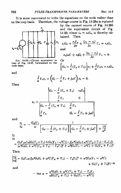
592 PULSE-TRANSFORMER PARA METERS [SEC. 14.3
It is more convenient to write the equations on the node rather thanon the loop basis. Therefore, the voltage source in Fig. 14.28a is replaced
by the current source of Fig. 14.28brL
m
and the equivalent circuit of Fig.14.29, where i. = cd%, is thereby obtained. Then
elrp + (el ~ ‘2) r. = edl~,Gcel rP C e2 ‘1 elG@ + ~Jw
i~= eaG~ and
(e2 – el) rL s ~.e~”uC + e2Gl +jw
FIG. 14.29.—Circuit equivalent to orthat of Fig. 14.27, formulated on thenode basis.
[ 1jwP+rLJ el+uG.–; lrLe2 = ed%j
and
Then( )~rLel+ GI–~rL+jtOC e2=o.
G. – ~ (r, + r’L) ec&
~ rL o(Al
e2 = P
f%–~(rp+rd ~rL
~ rL Gz–#’L+jucu
andez G.jrL 1—= ——
[ 1[
JeQ U
1f%–~(rp+rL) G1–~rL+j@ +2ez—e.
_ G.rm(kIIGi(rP+r.) +G.(rL–de)] ‘j[tO%&+@2C(rp+rL) – rpr.])– [@@@l+ UzC(r# + rL) – rpr.]’+ U’[aG(r.– @’C) + G1(rp+ rL)]’”
Then
ez— = (%r.to{ [dt%@ + LO’c(rp + rL) – rpr.]’ + @2[G.(rL – @’C)e.
+ GJI’P + rL]2}-%and
uW%l + uzc(r~ + rL) — ‘prL.– ‘an q = u[al(rp+ rL) + (%(rL – U2C)]

SEC. 14.3] EFFECT ON FREQUENCY RESPONSE 593
If all quantities are referred to the impedance level of 1/GI = 1 ohm,and if GO = Gl, then
ez– = r.(J)([U2 + fJ2c(r@ + r.) – r~r.]z + f.02[ZrL+ r, – 6)2C]2]-%,eO
Usually
& <<&L or rp << rL.P
Hence
e2– s rL@([U2 + @2CrL – rPrL]2 + @’[–@*c + zr.]2)-Heff
and
–tanp=(J2+ @*Cr. — rpr.
~(2rL — dc) “
If C is assumed to be approximately equal to C., the distributedcapacitance of the transformer, the characteristic impedance of thewinding may be chosen equal to the load resistance, that is,
‘AE=Jz=k=’Oh (13.4)
Also, since
and
or
T.t = @L-E, (13.5)
r
2LL(C2+I%.,=7= ~ (13.6)
P
C.= LL=~,
rL = :T)
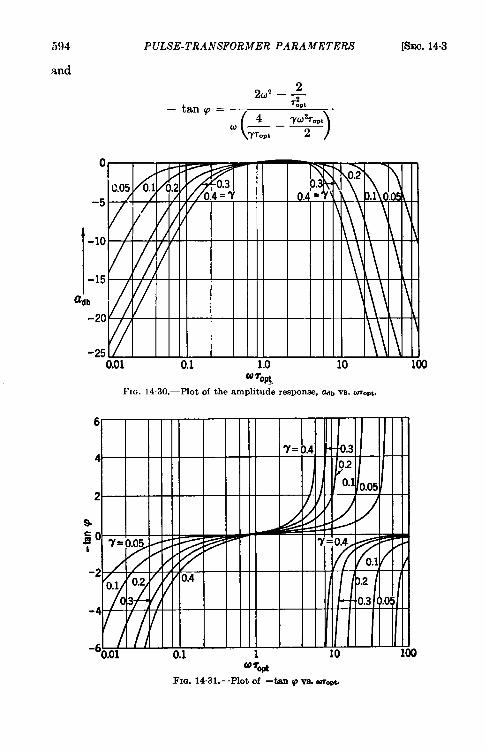
594
and
PULSE-TRANSFORMER PARAMETERS [SEC. 14.3
2(N – ~–tanp= T%
(
4
)
[email protected] —— —
-fToDb 2
0
-5
I-lo
-15
adb
-20
-250.01 0.l 1.0 10 100
~ TOpttFIG. 14.30.—Plot of the amplitude response, m~ VS. moP~.
@7*
FIG. 14.31.—Plot of -tan P va. w-

SEC. 14.3] EFFECT ON FREQUENCY RESPONSE 595
The response of the transformer may be expressed as follows:
II&=2010g102Q.e.
In Flga. 14.30, 14.31, and 14.32 are plotted respectively % vs. ti~,— tan ~ vs. Ww,, and – p vs. W=, for several values of (a i- &.t = Y.
cormFIG. 14.32.—Plot of -? vs. urmt.
Transformer,wdtagestepupratio= n
TRa
CkcMXcope 4plates
FIG. 14.33.—Circuit for oscilloscopepresentation of the frequency-responsecharacteristics of a transformer.
4+/Y i?
b ,’(
//
/
/FIG. 14.34.—Appearance of
oscilloscope trace with the circuitof Fig. 14.33.
It is to be remembered that the equivalent circuit from which thesecurves are calculated is valid only when LL is very small compared withL,, and hence when y is small. As ~ becomes larger, the error involved inusing thk equivalent circuit becomes greater. Hence, these curves. .-. ---
Fm. ‘14.31.—Plotof -tao q vs. --

596 PULSE-TRANSFORMER PARAMETERS [SEC. 14°3
tion. It has also been $ssumed that L, is constant over the frequencyraw shown. This assumption is valid only if the laminations are thinenough and their resistivity and P so high [see Eqs. (15.30) and (15.31)1thst the impedance of R, is high compared with that of Le over the fre-quency range considered.
It is possible to use oscilloscope presentation for the measurement of!eJed and tan Q by using the circuit shown in Fig. 14.33, where the
(d) 500kclcec, 9 = –26.6”. (e) 750WSCO. @ = -26.5°. W 1 molm. @ - –26°.
(u) 3 mc/ccc, O = –21”. (h) 5 mcleec, O = – 14°.FIQ. 14.35.—Photographs of oscilloscope presentation of the frequency-responec character-
istics of a puke transformer with n = -1 and RI = Ro = looo ohme.
actual generator has an impedance that is small compared with RO = RI.The oscilloscope traces are of the general form shown in Fig. 14,34,
where
Ide2 tan e. —,Q n
and
@b = 20 loglo +!2

SEC. 14.3] EFFECT ON FREQUENCY RESPONSE 597
In the measurement of frequency response it is often convenient touse two identical transformers, one a stepdown, the other a stepup, inorder to make n for the pair equal to one. The slope tan Ofor the com-bination may then be obtained and compared with the slope tan 0’obtained when no transformer is used in the circuit. Then le,/eal for the
(a) 1 kc/ccc, B = 5“, (b) 10 kc/see, 0 = 21°, (C) 20 kc/see, O = 23.5°.
~>1~1~~(d) 500 kc/see, O = 27”. (e) 750kc/eec, O = 26.5, (fl I mc/ccc, @ = 26”.
(Q) 2 mc/ccc, o = 11.7”. (h) 3 mc/eec, O = -11.1”.
(a] 4 me/see, O = –6”. (j) 5 me/see, @ = -3.5°.
FIG. 14.36.—Photographs of oscilloscope presentation of the frequency-respcmec character-istics of two pulse transformers (n = ~ and n = 5) with resultant n = 1.
transformer pair is equal to tan O/tan 0’. This method is recommendedbecause it eliminates errors arising from lack of orthogonality of the scopeplates.
In Fig. 14.35 are show? photographs of scope traces obtained atvarious frequencies in the measurement of the frequency response of atransformer that is operated with n = – 1 and RI = 1000 ohms.

598 PULSE-TRANSFORMER PARAMETERS [SEC. 143
F@re 14.36 shows similar photographs for a combination of trans-formers (232AW2 and 232BW2, see Tables 13.1 and 13.2) stepdownn = ~ – stepup n. = 5 operating into a load R1 = 1000 ohms.
Figure 14.37 shows the oscilloscope traces obtained when the trans-former or transformers are omitted from the circuit.
It is thus possible to relate, both theoretically and experimentally, thepulse and frequency-response characteristics of a transformer.
(a) 1 kc/eec
rl‘+(d) 500 kc)ecc
~~,
,:b) 10 kc/see (C) 20 kc/see
(e) 750 kc/see (f) 1 me/see
(0) ~ me/ccc ot) 5 me/see~lc. 14.37.—Photographs of oscilloscope presentation of the trace without the transformer
in the circuit, O = 28° for all frequencies, RI = Ra = 1000 ohms.
This chapter has treated the effect of pulse-transformer parameterson the pulse shape generated by power pulse generatom when resistanceand magnetron (or biased-diode) loads are used. The effect of the pulse-transformer parameters on the behavior of a regenerative-pulse-~ neratorcircuit has been outlined. The effect of the parameters of stepup andinverting transformers on the frequency response with a resistance loadhas also been discussed.
CHAPTER 15
MATERIALS AND THEIR USES
BY W. H. BOSTICK
CORE MATERIAL
16.1. D-c Properties and Test Results.—It
IN DESIGN
has been pointed out inSees. 12.2 and 13.1 that the primary or shunt inductan~ L, of a pulsetransformer must be large compared with the leakage inductance LL if thetransformer is to have a high efficiency. To achieve a low value ofL./LP it is necessary to make a wise choice of core material and type ofcore in designing the transformer. It is therefore of importance toinvestigate the factors that influence LP (or Le and R.).
Required Geometrical and Electrical Properties of the Core.—In general,the core should be made in the form of a closed path with a mean mag-netic-path length as small as the coil that it encloses permits. In orderthat eddy currents may be reduced, the core must be fabricated from thinlaminations or strips, and the core material should have as high a resis-tivity as is consistent with the retention of good magnetic and workingproperties of the steel. The rolling of the magnetic material into thick-nesses in the range of 0.001 to 0.005 in., and the fabrication of this mate-rial into the core, must not seriously reduce p., alter the shape of theB-H loop in the vicinity of BU,, or increase the value of H. (see Fig. 15.2)of the material. Furthermore, it must be possible in one way or anotherto assemble the coils on the core or vice versa. The interlaminar resist-ance must be sufficiently high to keep the eilect of interlaminar eddycurrents negligibly small, and the thickness of the interlaminar insulatinglayer should be small enough to permit a high space factor (ratio of activevolume to total volume) for the completed core.
D-c Properties of the CoTe Material.-The pulse properties of a coredepend to a great extent upon the d-c or low-frequency properties of thecore and the core material. The d-c magnetic properties of a core thatare relevant to pulse-transformer use will now be discussed.
Usually voltage pulses of only one polarity are applied to the trans-former, and under these conditions the core material is operated only inthe region to the right or left of the H-atis. If the pulse-transformercore is initially unmagnetized, and rectangular pulses of constant voltageand one polarity are applied, the resultant incremental B-H loops of
599

600 MATERIALS AND THEIR USES IN DESIGN [SEC. 15.1
constant flux swingl AB will, during a brief transient period, bring thecore material to the state where the loop from the remanent point to theB-H curve has a change in flux density equal to AB. The location of
FIO. 15. 1.—St.38dy-st8te d-e incrementalB-H loops showing the remanent values ofB for various valuee of Al?.
coil and the cross-~ ctional area of
the remanent point depends uponthe particular value of AB and onthe shape of the B-H curve (seeFig. 15. 1). If AB is large, theremanent flux density at the begin-ning of each pulse (after the tran-sient period is over) is very nearlyequal to B,, the remanent fluxdensity of the core when the ma-terial is driven to saturation.z
It is often desirable to have alarge AB during the pulse in orderto” keep the number of turns on the
the core reasonably small [see Eq.(10)]. With a material of large remanent induction B, (see Fig. 15.2a)the AB over which the core may be operated during the pulse withoutsaturation is small.
TjB; 0,AB” /
(a) (b)FIG. 15.2.—D-c hystereeie looP of s core with (a) a continuous magnetio cfmuit (no butt
joint), (b) a gap in the magnetic tircuit.
From the d-c or low-frequency hysteresis loops of two sample cores,one without butt joints shown in Fig. 15.2a and the other with butt joints,
1In the discussionof the d-c propcrtieeof the core material, AB and B are ussdineteadof ~ and ~, which are used in the discussionof the pulse propertiesof thecore to denotevalues of flux density averagedthroughoutthe laminationthickness.
2In the computationof the optimum gap lengthin the core and of the valuesof pwhena revemecurrentis employed,it is assumedin thissection,for purposesof simpli-fication, that A~ ie so large that the resultantremanencealways ~rreaponds to theB-H loop of the core materialdriven to saturation.

SEC. 15.1] D-C PROPERTIES AND TEST RESULTS 601
(that is, gaps in the magnetic circuit) shown in Fig. 15.2b, itis obviousthat B, may be reduced (and the available AB thereby increased) by—
1. The insertion of a gap (a butt joint) in the core (see Fig. 15.2b).2. A reverse magnetic field H, (see Fig. 15.2a) produced by a current
that flows through the primary in the reverse direction betweenpulses and leaves the core with a remanence B = l?: (and H = O)
at the beginning of each pulse.3. A reverse magnetic field H, produced by a constant reverse current
(in either the primary winding or a special winding in the trans-former) that leaves the core material at B = l?:’ and H = – H, atthe beginning of each puke (see Fig. 15.2a).
To achieve a value of B, that is well below the B-axis (and hence ahigh available AB) by Methods 2 and 3 without requiring an inordinately
= lg
T
FIQ.15.3.—Idealized d-c hysteresis loop of a pulse-transformer core.
large amount of current to achieve the requisite H,, and to achieve a highaverage d-c incremental permeability pi, it is obviously desirable to ha~ea very low He. To achieve a low B, by Method 1 without introducingan extremely large gap (which markedly reduces p.~ and W) it is alsodesirable to have a low H, [see Eq. (4)]. The available AB is alsodependent upon BM,, the saturation induction of the core material; thus,other things being equal, it is desirable to have a core material with ashigh a value of B.., as possible in order to obtain a large variation in fluxdensity.
The average incremental d-c permeability pi over the range AB is, inmost cases, a major factor in determining the pulse permeabilityy. It istherefore desirable to have ~ a maximum.

602 MATERIALS AND THEIR USES IN DESIGN [SEC. 15.1
Optimum Gap Length of the Core.—Most low-power pulse transformersoperate with relatively small values of AB (less than 1000 gauss), and inmany of these transformers no special precautions need be taken toreduce B, (see Fig. 15.1). With high-power pulse transformers, however,it is often advisable to use a large Al?. In many high-power applicationsa gap, rather than reverse current, proves to be the more practical methodof reducing B,
It is possible to calculate approximately the gap length necessary toproduce maximum w over the range AB if the hysteresis loops of Fig.15.2a and b are assumed to become, through a process of idealization, theloops of Fig. 15.3.
It is sometimes desirable to increase the induction during the pulsealmost to saturation in order to achieve the maximum Al?. Therefore, itis assumed that the valve of AB that is effective during the pulse is
AB = B.., – B,a,
where B,g as defined in Fig. 15.3 is the remanence of a core containing agap.
The magnetomotive force H1 may be equated to the flux multipliedby the sum of the reluctances of the core material and the gap. Thus,
‘Z=BA(+O+9=B(:+’J”Then
lH—s. .B
~+;,% PO
or
where 1is the mean magnetic-path length of the core and is assumed to beessential y equal to the total magnetic-path length of iron and gap, 10is the gap length, and A is the cross-sectional area of the core. FromFig. 15.3 it is evident that
B, = p.H,,
B,. = p.vH.,
and
Since a gap is usually chosen in practice so that B,a << B-,, the followingapproximation can be written for thk last equation:

SEC. 15.1] WC PROPERTIES AND TEST RESULTS 603
(2)
It is desired to maximiae p with respect to 1./1, that is, dpiO/d(lo/l)
should be equated to zero. Since
and dp.O/d(lg/l) vanishes only for ye = O, and p. is always greater thanzero in practice, the value of gap length for maximum w, may be obtainedfrom the relation
or4H.
I+ P.; –B= p. = o.
From this relationship, the optimum ratio l./l for a core that is to bedriven almost to B-, is
()1j 4H, 1——— .1 out= B-, p.
(3)
The value of w, for this optimum length of gap is given by
If, for a given material with no gap in theB; = jB~,, where ~ is some fraction less than 1,
(4)
core, the remanence
()10
7 ()=:(4f–l) =&t 4–;.
opt
In most core materials used in pulse transformers, j = 0.75. Then
()1~ 21 .,, = g“
Thus, the optimum gap length for a Mo permalloy core (H. = 0.04oersteds, Bout = 8500 gauss) is about one-third the optimum gap lengthfor a Hipersil core (H, = 0.25 oersteds, B=, = 17,500 gauss’), and the
1Complete ferric saturation occurs at B = 20,250 gaoss. For purposesof con-structingan idealizedd-c B-H loop, however, B-t = 17,500 gauesis a moresuitablevaluefor Hipersil.

604 MATERIALS AND THEIR USES IN DESIGN [SEC. 15.1
value of h for the optimum gap length is about three times as great forthe Mo permalloy core as for the Hipmsil core.
A typical 0.002-in. Hipersil core with 1 = 5 in. is manufactured with abutt joint containing a total gap length of about 0.001 in. Thus
~ _ 0.001 in.1l– 5 in.
= 2 x 10⁻⁴,
The value of p. for this material is about 10,000, for which
()1~ 2.—.1
2 x 10–’.opt PO
Thus, the gap used is approximately of optimum length if the core is to bedriven almost to B-,.
The value of ~i~ calculated from Eq. (4) in terms of P. for l./l =(1./1)09, is
“U= *If j = 0.75, Pi. = Po/f3.
The quantity p~~ (see Fig. 15.3) is related to p. by the followingequation:
pm, = <;Hc=(.::’.)’O’+’OHence, when
When j = 0.75,
Pig = o.3pmx.
()It is to be remembered that the foregoing values of ~ and ~i~areout
calculated for a core that is driven to B-,. If it is desired to drive theflux density to some value B- that is less than B~,, but still much greaterthan B,,, Eq. (2) becomes
and Eq. (3) becomes

SEC. 15.1] D-C PROPERTIES AND TEST RESULTS 605
Effect of Reverse Magnetic Field.-For some applications in which highvalues of AB are required, it is not only practical but advantageous to usea reverse current (usually with anungapped core stmcture). Thefollowing analysis of the effect ofrevense current holds for cores,whether they have a gap or not,as long as their d-c hysteresisloops are approximately repre-sentable by the idealized loop ofFig. 15.4.
The quantity By is defined ssthe induction that results fromthe application of a d-c reversefield H,. It is assumed, for sim-plicity, that the remanent induc-tion By resulting from theapplication of a peak reverse field
,a
B%.
B;= B:
H—
L/lFto. 15.4.—Ideahzed d-c hysteresis loop
depicting the operation of a core with eithera d-c H,, or a peak reverse H, between pulses.
H, between pulses (which drops to aero just before the beginning of thepulse) is equal to By. Thus
B? = B; = (H. – H,)p..
The value of ~i that results from
AB = B. – B~,
where H, is applied as a peak reverse field between pulses and fails to zeroat the beginning of the pulses, is
B* – By = Bm – (H, – H,)po.~:’ =
H.+% Hc+~
It is possible, if desired, to express pj’ in terms of pm since
B~u= “ .
H.+%
ThenBw,flm
‘“ = B=, – H,P-’and
(5)

606 MATERIALS AND THEIR USES IN DESIGN [SEC. 15.1
R------6 3-----
----. 4----
(a)
(d)
(9)
@
-----
-.—---
01
El----
6 %-----
-----% *----
(b) (c)
@@(@$)---- ----(e) if)
❑✍✍✍✍✍✍✍✍(h)
D--::--_JL--(m)
H----l_——_
—— __
-— __
(k)
DI--------
H-----—-.---_—--
(?1)
~[
--—----
------
(1)
Fm. 15.5.—Diagrams showing various types of pulse transformer cores.(a) Continuously-wound strip core.(b) One butt joint sawed in a continuously wound strip core.(c) Two butt joints sawed in a continuously wound strip core.(d) Two butt joints sawed in a continuously wound strip core. Coils are wound in ordinary
fashion with half core ae a mandrel.(e) Laced-joint core. Core is continuously wound from strip, annealed, every third leal

SEC. 15.1] D-C PROPERTIES AND TEST RESULTS 607
If H,is obtained from a constant d-c current in one winding of thetransformer, the resultant incremental permeabilityp~” over
AB=B. —B~
is,,, _ En – (H. – H,)p..pi —
H,+Hef~
(6)
It is also possible to express ~{” in terms of p= if Eq. (5) is substituted inEq. (6).
- Fo; materials such as the permalloys, where a reverse current maybeadvantageously used, po is usually very high and a suitable value for thereverse field H,, in order to obtain a high p: or ~~” is H, < H, < 2HC.
Values of H, greater than 2HC are, of counse, advantageous if they can beobtained. From the idealized loop of Fig. 15.4 it may be seen that, if
H, =H.+~,
the highest possible value of ~~’ is obtained. This highest value of ~~”equals g-,, which is approximately equal to p./(l + fl.
Geometrical Core Shapes and Types of Construction That Have Been
Evolved.—A number of methods of constructing cores have been evolvedby various British and American manufacturers. These arrangements ofcore material are described and numbered in Fig. 15.5. With cores thatcontain no gap (that is, cores of either lap-joint or continuous-strip con-struction) it is necessary to have a reverse magnetic field H, if AB is to befairly high. Under these conditions, it is desirable that the magneticmaterial have a low HC in order that the H, available between pulses orfrom a d-c winding may reduce the remanence to a low or negative value.If the core is an unbreakable closed magnetic circuit, it is necessary towind the coils by hand with a bobbin, or on a machine with a circularshuttle.
cut as it is disassembled. The pieces sre then reassembled into the Cu coils. This corehcs 8 poor space factor.
(f) Long strips are laced into completed coils. This method is tedious for thin laminationsand large transformers.
(u) COre is cOntinuOusly wOund ~th extra window length, annealed, and cut at one end.The core is inserted into Cu coils and the ends of the magnetic strip are interleavedto form a lap joint.
(h) Alternate-stacked lap joint.(~) Same ae (h) except that the laminations are all cimilarly stacked to give a butt joint.f.j) U-U punchings, lap joint.(k) U-I or L-L punchingewithlap joint.(1) U-I punchingswithbutt joints.(m) E-E stacked,butt joints.(n) FourI’s stscked,lap joint.

608 MATERIALS AND THEIR USES IN DESIGN [SEC. 15.1
Iron-dust cores for pulse transformers have, in general, proved inferiorto laminated cores because of their large inherent effective gap, and hencetheir low effectiw. permeability.
The magnetic materials manufactured in the United States and theUnited Kingdom, together with the types of pulse-transformer cores inwhich the materials have been used, are listed in Tables 15.1 and 15.2.
TABLE15.1.—COREMATERIALSMANUFACTUREDANDUSEDIN TEEU.S.A.
Material
787. Ni, 3 %Mo, 19% Fe,Permalloy0.0012 in.
45% Ni, 557.Fe, Permal-10Y0.002 in.
457. Ni, 557.Fe, Pernml-10Y0.C02 in,
4590 Ni, 557.Fe, Perrnal-10Y0,002 in.
45% Ni,3%Si52% Fe, Silicon Nicaloi0.002 in. and0.004 i“.
459. Ni, 3 %Mo, 52% FeM .“inmx0,M)2 in,0.003 in, and0.004 in.
3% Si, 97?4Fe, Si Steel0.003 in.
3 % Si, 9790Fe, Hipernil.002 in.
Oriented0.002 in.0.001 in.
k.e ofcore
.)
.), (b)(c) , (d)
O), (b)(c) , (d
e). (f),(a), ex.peri-rnenta
e), (J’)sand (0
e), (1-)U);tYFe cin ex.peri-mentaquantity 0“1!), (1),(Jtype(c) anc(e) irexperi.menta
wan.e)
Type of inter-laminsr imulation
SiO, dust depositedby cataphoresin procm
SiO, dust depcmitedby cataphoreain; ormica dust
Mica dust
Oxide
Chrome ❑ilitate, cOl-loidal silica
Oxide
Oxide and powder(MgO)
Carlite coating (ironphmphate)
Materialmanuf sc-
turer
FIe!stemElectricco.
Weater”Electricco.
Carpenter
AlleghenyLudlum
AlleghenyL“dlum
AlleghenyL“dl. m
AmericanRollingMill Co.
CoreIlm”uf ac-
turer
Ve.stsrnElectricco.
WesternElectricco.
$fsgneticMetals
co.
MagneticMetakco.
>eneralElectricco
>neralElectricco.
2eneralElectricco.
Westing-
houseElectricCorpora.tion
Principal“~ern of
coma
Veder”Electric Co
westernElectric Co
WesternElectric, Co
RadiationLaboratory
GeneralElectric Co
GeneralElectric Co
GenernlElectric Co
Westing-
house Elec.tric Cor-poration,GeneralElectricCo., Ray.theon,Utah, andothers
Pufse-pOwerrmge in which:ores are gen-erall y used
IO-1OO kw
100kw-1 Mw
100kw-1 Mw
[00 kw-1 Mw
).1 kw-1 Mw
).1 kw-1 MW
10kw–O.5Mw
1 kw-3 Mw25 kw-10 MW).1 kw-1 Mw3.lkw-10kw

SEC. 15.1] D-C PROPERTIES AND TEST RESULTS 609
TABLE 15.2.—CORE MATERIALS MANUFACTURED AND USED IN GREAT BRITAIN
Material
Radiometal0.CQ4in.
Rmdiometal0.004 in.
Radiometal0.004 in.
Radiometal0.002 in.
Radmmet al0,002 in.
Radiometal0.005 in
Rhometal0.004 in.
Rhometal0.0Q4 in.
Rhornetal0.004 in.
Rhornetal0.004 in,
Rhornetal0.003 in.
Rho metal0.002 in.
4% Si, 96%Fe, 0.007in. O.014in
Stalloy 0014in.
Type ofcore
(h)
(h)
(n)
(e)
(.)
,.,
(h)
(n)
(n)
(n) or (e)
(u) (n); (c)experimental only
(a)
(n)(n)
(n)
Type of inter-Iaminar insulation
Oxide; sometimes lSC.quer m weU
Paper interleaved
Oxide
Lmq”er
Varnish
Oxide
., .,,...
Oxide
Lacquer
Materialmanufacturer
Magnetic andElectric Al-loys
Magnetic a“dElectric Al-loy*
TelegraphConstructionand Mainte-
nance Co.,Ltd.
Magnetic sndElectric Al-loys
Magnetic andElectric Al-loy,
core
rmnuf rwtme
Magnetic amElectric Al10YE
bfagnetic a“,Electric Alloy~
tie,gnetic a“,Electric Al10y8
ilagnetic amElectric AlIoy.
Principal wraof cores
The General Elec-tric Co. Ltd.(GEC) BritishThompmn Huato”
Co. Ltd. (BTH)BTH
Metro politan-Vick-cm Electric Co.,M. (METV)
BTE
BTH
GEC
GEO
E. C. Cole Ltd.
GEC
METV
METV
BTH
METVMETV
hlETV
Equation (1320) shows that, in order to make the value of (a + ~)~.,low (that is, to make the efficiency high), the effective pulse permeabilityP. should be made a maximum. As is shown later, p, depends upon thepulse duration, the thickness of the laminations, and the values of theresistivity and the permeability ~; of the material. Other things beingequal, it is of advantage in the design of a transformer to select the corematerial and type of core that provide the highest value of ~i. There is,however, a dependence of (A~).p, on load impedance, power level, wiresize, and ~e (see Eq. (13.17)]; also, the value of pi for a given core dependsmarkedly on Al?.

610 MATERIALS AND THEIR USES IN DESIGN [SEC. 15.1
A workable procedure in the choice of core material and core for apulse transformer is to estimate a reasonable value for ~,, and from thisestimate to determine the approximate value of (Al?)o, by the use ofEq. (13.17), past experience, and extrapolation from previous successfuldesigns. The core material and structure giving the highest pi for thisAB are then selected,
For regenerative-pulse-generator and interstage transformers oper-ating at pulse powers of the order of magnitude of 0.5 kw, (A~)~~t is ofthe order of magnitude of 1000 gauss. For pulse transformers operatingat pulse powers of the order of magnitude of 0.001 kw, (A~)w, is much lessthan 1000 gauss. For the transformers that operate at very low values
Fm. 15.6.—An assortment of widely used 0.002-in. Hipereil pulee-transformer cores.
of A~, it is advantageous to use cores without any gaps and with thesteepest incremental B-H loops (see Figs. 15.1 and 15.2), which are foundin materials of low H, and high ~o (that is, the permalloys).
For transformers that operate at high power levels (A@m, is of theorder of magnitude of 8000 gauss. If sufficient reverse current is avail-able, the highest value of ~i can usually be attained by using a permalloycore with no gap. If these cores are continuously wound from ribbon, thewinding of the coils for the transformer must be performed with a shuttle.This departure from the simple normal practice of coil winding and thefact that the core window cannot be used so economically if shuttle wind-ing is required may in some cases induce the designer to choose a corewith a gap.
The designer is obliged to choose a structure that contains a gap ifinsufficient reverse current is available. The advantage that the mate-rials with very low He and very high p. (that is, the permalloys) have overoriented silicon steel in ungapped structures is largely lost in gapped
-.-.,, ~..~ ~~‘~==uq. ~~-wx#.JJ,mau7 CIIGviaiw IX pi 10r a given “core aepehas ‘markedly on AB,
f4$(

SEC. 15.1] D-C PROPERTIES AND TEST RESULTS 611
with both types of materials with the various gapped structures illustratedin Fig. 15.5. From the point of view of the ezse of constmction of the
FIG.15.7.—Vmious uncut Ni steel pulm-transformer cores. (a), (b), and (c) O.001-in.Mo permalloy cores. (d) and (e) 0.002-in. 45-permalloy cores.
transformer, of a high available AB, a reasonably high value of ~i, a highspace factor, the availability of light gauge materials in large quantities,and the uniformity in the com-pleted product, the type C core(Fig. 15.5) ut ili zing 0.002-in.Hipersil has been an extremelyuseful pulse-transformer core. Anassortment of widely used sizes of0.002-in. Hipersil cores is shownin Fig. 15.6. Various O.001-in.Mo Permalloy and 0.002-in. 45-Permalloy uncut cores are shownin Fig. 15.7. Several 0.004-in.silicon Nicaloi punchings and one0.003-in. M on i m a x punchingwidely used in pulse transformersare shown in Fig. 15.8.
Standard Tests on Core Mate-
m“als and Cores.—l’here has beenan effort on the part of the agen-cies interested in pulse trans-formers and on the Dart of
FIG. 15$.-Various nickel steel punrh-ings. Light-colored punchmgs are of 0.004-in. silicon Nic8bi, the dark punching of0.003-in. Monimax.
industries manufacturing them to formulate a set of standard testson pulse-transformer cores and core materials to facilitate the con~-parison of the various cores. This set of standard tests for pulse-t rans-former cores is set forth in the Radiation Laboratory Report h’o. 722.’
1W. H. Bostick, “Pulse Transformer Committw Stmd:mf Test hlethods forPulseTransformerCores,” RI, Report No. 722, Nlny,5,1945.

612 MATERIALS AND THEIR USES IN DESIGN [SEC. 15.1
The measuring techniques given in that report are described in Sec. 15.2.Results of Tests on Various Core Materials. -In Table 15”3 are listed
the results of a series of systematic measurements made in 1944 on severalwidely used materials for pulse-transformer cores manufactured in theU. S.l These results show that Hipersil excels at the high values of A~,tmd that the Ni steels are better at the lower values. The pulse per-formance of Mo Permalloy when a reverse magnetic field is used isespecially notable.
Fm. 15.9. —LOei ofCurveCurveCurveCurve
// / ,//, /
i 4,000- i ‘//I
//x
‘WYktH—H,Opnmrl5 10 15 20 25 30
H inwstedsthe tips of pulseB-H loops taken on but&joint coree, titb 1A is for Monimax 0.003-in., } in. by + in. leg section.B is for silicon Nicaloi 0.003 in., } in. by } in. leg section.C is for silicon Nicsloi 0.004 in., + in. by ~ in. leg wction.D is for Hipersil 0.002 in., } in. by i in. leg eection.
-~sec pulses.
In Fig. 15”9 are shown the loci of the tips of B-H loops obtained withl-~sec pulses for several cores constructed of punched laminations withbutt joints and for a type C Hipersil core. Again it may be seen thatHipereil excels at the Klgh flux densities whereas some of the nickel steelsappear slightly better at lower flux densities.
Actual photographs of pulse B-H loops are shown in Fig 15.10.The d-c and pulsed B-H loops shown in Fig. 15.11 are representative
of the performance of British pulse-transformer cores, which were made,for the most part, of nickel steel. The construction of “synthesized”pulsed B-H loops shown in Fig. 15”11 will be described in Sec. 15-I.
I Although more accurate measurementshave subsequently been made, themessurementalisted in Table 15.3 provide a reliable basis for a comparison of tbevariouscore materiafs.

SEC. 15.2] PULSE MAGNETIZATION
(a)
I
r-—- J
> --_—(a)
—
L“r .-
—..-—. ..—J(b)
!.-1
lJ..—..ji-
(c)
rL.(f)
613
Flo. 15. 10,—F’hotogrsphs of oscilloscope traces Of pulse B-H Ioops at various pulsedurations. ~ is vertical and H is horizontal.
Core MakerialN
turns
200100
2=100
%10050
Aiiw = ~H ‘ax
540370200
l:g
340260440350
Space factor6O.OO1-i”. coren. . . . . . . . . . . . . . . . . . . . . . ...0.850.002 -i”. am10,003in . . . . . . .,, . . . . . ...0.95
2i-iIa. wind.no core8A = 2.stl cm:l=17cln
15.2. Pulse Magnetization. Electromagn.dk Treatment oj the Mag-
netization oj the Core.—The theoretical expression for the inductance andmagnetic field of a coil of given length and diameter involves Nagaoka’sconstant, which depends upon the ratio of length to diameter of the coil.However, if the coil is wound in the form of a toroid, its inductance is

TABLE 15.3.—D-c AND PULSE DATA ON SEVEItAL WIDELY USED CORE MATERIAIA MANUFAIXURED IN THE U.S.A.
Material . . . . . . . . . . . . . . . . . . . . . . . . . . . . . . . GE Si Nicaloi (B9W)
Ckmstitution. . . . . . . . . . . . . . . . . . . . . . . . . . . 42.6570 N0.40?4 Ml0.34% Al3v. sl
Thickness of lamination,in... . . . . . . . . . . . 0.0025Specificgravity. . . . . . . . . . . . . . . . . . . . . . . . . 7.9Reeistivityin microhm-cm.. . . . . . . . . . . . . . 85
D-c magnetizationdata. . . . . . . . . . . . . . . . . . Uncut corlp-.. . . . . . . . . . . . . . . . . . . . . . . . . . . . . . . . 7650H in oersteds at
B=lOOO gauss . . . . . . . . . . . . . . . . . . . . 0.18B = 5000 . . . . . . . . . . . . . . . . . . . . . . . . . . 1.02B=lO,OOO. . . . . . . . . . . . . . . . . . . . . . . . . . . . . . . . .B = 12,500 . . . . . . . . . . . . . . . . . . . . . . . . . . . . . . . . .
Bingauss at H = 25 . . . . . . . . . . . . . . . . . 9800At B=5000gause . . . . . . . . . . . . . . . . . . . .
H.inoersteds . . . . . . . . . . . . . . . . . . . . . . 0.195B,ingauae . . . . . . . . . . . . . . . . . . . . . . . . 2750
Imss in ergs/cmS/cycle (60 cycles) . . . . . . 265At B=lO,OOOgause . . . . . . . . . . . . . . . . . .
H,iningauss oereteds . . . . . . . . . . . . . . . . . . . . . .B,ingauw . . . . . . . . . . . . . . . . . . . . . . . . . . . . . . . . . . .
Loss inergs/cm’/cycle . . . . . . . . . . . . . . . . . . . . . . . . . . .
42.4Y. NI3.33% Mr0.75% Al
0.0047.985
Uncut core37,000
0.050.133.71
. . . . . . .,11,950
0.059430089
0.087250390
GE Monimax
47% Ni3% Mo
0.00258.4573
Uncut core21,900
0.090.243.1713,813,400
0.113580120
0.135500475
cut core *
2680”
0,41’1.92”9.0”22.4”12,900
0.13530140
0,20950520
WE MOPermalloy
79% Ni4% Mo
0.00128.746
!Jncutcore79,650
0.030.065
. . . . . ,.,. . . . . .
“8880
0,045397040
. . . . . . . .,. .,... ,.,. . . . . . . . .
Westinghouse orientedHipereil
3.2(
0,00257,650-55
Uncut core12,200
0.200.460,851.4517,400
0.2733360280
0.388080820
6 Si
Cut core6180
0.330.831.712,8516,500
0.2572100420
0.4547001450
—.— “. -— . .._

Material. . . . . . . . . . . . . . . . . . . . . . . . . . . . . . GE SiNicaloi(B9W)
Pulse magnetization datar = l~ec
For H, = OH in oereteds at A? = 5000 gause. . . . 7.1
at AB = 1500. . . . . . . . . . 22.5at A~=lO,oOo . . . . . . . . . . . . . . . . . .
For H, = 0.5 oerstcdsH in oereteds at A~ = 5000 gauee. . . . 4.5
at A~ =. 7500 . . . . . . . . . . 6.9at A~=lO,oOO . . . . . . . . 9.7at A~ = 12,500 . . . . . . . . 13.0at AB = 15,000 . . . . . . . . . . . . . . . . . .
For H, = H.H in oersteds at A~ = 5000 gauee. . . . 5.25
at A~ =- 10,000 . . . . . . . . . . . . . . . . . .I.oss in ergs/cm’/p~lee
ntAB = 5000 . . . . . . . . . . . . 108Oat A~=l O,ooo.. . . . . . . . . . . . . . . . . . .
45.0. . . . . . . . . .. . . . . . . . . .
4.37.511.315.6
. . . . . . . . . .
8.1. . . . . . . . . .
2164). . . . . . . . . .
GE Monima%
5.911.633.3
2.64.15.87.69.8
3.27.2
6852115
7.2*11.6”16.25”
7.1”10,8”14.8*19.1*
6.65*15.4*
985 *3840’
WE Mo WeatinghouaeorientedPermalloy Hipereil
. . . . . . . . 30.0 7.0
. . . . . . . . . . . . . . . . . . 10.2
. . . . . . . . . . . . . . . . . 14.3
1.0 4.8 5.21.75 6.5 7.52.7 8.5 9.93.7 10.1 12.5
1.1 5.25 5.75. . . . . . . . . . 8.4 10.1
Teats were performed on strip-wound ring mmples # in. by 4 in. in arms 8eotion, and with m incide diameter of 2 in. All results are reported on the bti ofnet mm area. Meamrementa were made under the direction of W. Merrill of the General Electrio Company, Pitta6eld, MM, 1944.
* Beoauoeof faulty outting,thegapin tti oore was mnsiderablylargerthanoptimum.

616 MATERIALS AND THEIR USES IN DESIGN [SEC. 15.2
and the magnetic field inside the coil is
~ = 4xN~101
oersteds, (7)
where 1 is the mean magnetic-path length of the toroid in centimeters, A
is the cross-sectional area of the toroid in square centimeters, and i is the
n WY It-1# I%thesizaPUG I I
00246810121416 18H inOersteds
FIG. 15.11.—Experimental and synthesi~ pulse B-H Ionps for British Rhornetal,No 8 punchings, oxidised and sprayed withlacquer; nominal thickness 0.004 in.: core inthe form of two E’s with 0.001 in. butt jointgap in each leg. M -7500 gauss, r = 1.0m.
current in amperes. If a toroidacore of effective permeability p.is inserted in this toroid, theinductance becomes
4mN2Ap,L=— 1091 ‘ (8)
and, since no free magnetic polesare formed, the magnetic field H
inside the coil is unchanged.If a coil is wound on the to-
roidal core so that only a fractionof 1is covered, and if P. >> 1, mostof the magnetic flux is still con-strained to remain in the core.The field H is still approximatelyconstant in magnitude and parallelto the center line of the toroidthroughout the whole of the core.
aa it is when the coil completely encloses the core. Hence, Eqs. (7) and(8) are good approximations for the inductance and magnetic field of sucha core and coil.
Under pulse conditions the effective permeability p. of the magneticmaterial is, because of eddy currents, different from p, the intrinsicpermeability of the material itself. It is, therefore, of importance tostudy the relationship between p. and p.
Relationship of V to B; Faraday’s Law.—At any point within the coil,or within the toroidal core if there is a core, the following equations (inmka units) of Maxwell are applicable:
vxE+~=O,
or
H vxE. dS+H
;.dS=O,
A A
where A is the area of the coil. By Stokes’s theorem, the emf per turn, inmks units, is

SEC. 15.2] PULSE MA(7NETIZA TION 617
(9)
where C is the perimeter of A and where the average flux density over thearea A is
B=: H B “ dS.
A
If B is exprewed in gauss and A in square centimeters, and if the coil hasN turns, the total voltage impressed across the coil may be written, inCgs units, as
NA dBv ——
= – 10s dtvolts.
Since V is constant throughout the pulse for the idealized pulse,
/
B
B= d~ =\-K ;Vd’=-%
gauss; (lo)o
that is, 1? increases linearly with respect to time throughout the pulse ifV remains constant regardleea of thequality of the core material or whetherthere is any core at all. The value of ~at the time t = r is denoted by the symbol
$
7;AD.
Development of the Diffm”on Equatiorw. tf’ 0):
It is now assumed that a toroidal core J%--
occupies most of the coil area, and that p. xl
is sufficiently high to constrain practically =all of the magnetic flux in the core. Thenthe area A is, for all practical purposes,equal to the net area of the core. It is alsoassumed that the magnetic field inmressed FIm 16.12.—Ide limtion of a Iami.
nation in a pulse-transformer core.at the surface of the core does not vary
along 1 and is everywhere parallel to the center line of the core. Theproblem is to find the magnetic field (see Fig. 15.12)
‘4’)=H(+)which, when applied to the surface of the core material, gives an averageinduction throughout the core of
D– Iosvt
‘--m- gaufw.

618 MATERIALS AND THEIR USES IN DESIGN [SEC. 15.2
It is apparent at the outset that the core material must be in the formof thin insulated laminations if eddy currents are to be held to a reason-ably low value. Figure 15.12 shows such a lamination in which the widthof the lamination in the x direction is practically infinite compared withthe thickness d. The z direction is assumed to be along the center lineof the core, and any current that flows in the coil produces a magneticfield in the z direction only. It is assumed that this magnetic fieldH,(y,t) does not vary with the coordinates x or z.
The following Maxwell’s equations in the mks system of units maybeemployed:
vxE+#=O,
In any known core material m is large and c1/co = 1, where C1and co arerespectively the dielectric constants, in mks units, of the material and offree space. Conduction currents are therefore so much more importantthan displacement currents that it is possible to neglect the term dD/dt.The symbol M is used to denote the permeability of the material in mksunits. Also, it is assumed that the permeability p (p, in mks units) of thecore material is constant over the range of induction through which thecore is to be operated. Then
andVXH=U,E,
where
Since
and
then
H.= HV=O.
H. j
vxH.~ ~ a aH= aHz_=i__j —,ax ay az ay ax
aHz _ ~
-i%–– ‘
aH,i — = iulE.,
ay

SEC. 15.2]
ancl
Then
PULSE MAGNETIZATION 619
EV=E. =O.
and since
The two equations
and
aHz~=
UIE=
aEz aHz
?Y—=plm 1
(11)
upon differentiation and subtraction yield the following diffusion equa-tions:
a2Hz aHz~ = “v’-x’
andd2E= _ aE.ayz ‘1”1 z“ I
(12)
Solution of the Diffu-sz”on Equations.-The solution’ of llq. (12) may bewritten as the sum of Ha(y,t), a‘’ steady-state” term or particular integral,and Ht&!,t), a transient term or complementary function (H= and Hb arein the z direction, but the subscripts z have been dropped for brevity ofnotation). The average value of Ha(y,t) across the lamination is assumedequal to (A~/r)t, where AH is the mean impressed field in the core at theend of the pulse of duration r.
1This treatmentfollows that given in the followingreferences:L. W. Redfearn, “The Effective Permeabilityand Eddy CurrentLose for Mag-
neticMaterialunderLinearMagnetization,” Metropolitan-VickersElectricCo., Ltd.,Report No. C.287, Feb., 1942.
C. R. Dunham, C. C. Hall, K. A. MacFadyen, “Calculation of Eddy Currents inPulse Transformer Cores,” The General Electric Co., Ltd., Report No. S350, May 8,1944.
For other trmtmenta that reach the same solution, see L. A. MacColl, Bell Tele-phone Laboratories, Inc., and T. D. Holstein, “Skin Effect in Pulse-TransformerCores,” Wmtingbouee Research Laboratories, Report No. SR-170, Feb. 22, 1943.

620 MATERIALS AND THEIR USES IN D-ESIQN [SEC. 15.2
Equation (9) when integrated
FIG. 15. 13.—Path of integration forobtaining the stead y-state distribution ofE. and H,.
over the area S (instead of A), asshown in Fig. 15.13, yields for thesteady state
2WEZ =II
aB~.dS=2wyd$,
ssince
Ha~ dn
at ‘Z
when the eddy currents have attaineda fixed pattern, that is, when thesteady state has been attained.
and the steady-state magnetic field associated with this E% can be obtainedby integrating Eq. (10) directly since the steady state E. no longerinvolves t. Thus, the steady-state magnetic field associated with E. is
Ha =\
di?
‘Ha = “ x 1y dy = constantly + constant~,
and the complete steady-state term or particular integral may be written
(13)
1 2
where Term 1 takes care of the constant rate of increase in Ha averagedthroughout the lamination, and Term 2 takes care of the spatial distribu-tion of magnetic field resulting from the steady-state pattern of eddycurrents.
A substitution of Eq. (13) in Eq. (12) yields
A2 = ‘+.
Also,
and hence

SEC. 15.2] PULSE MAt7NETIZA TION 621
Then
(14)
It is apparent that the transient term or complementary function Hbhaa its maximum at y = O and decays exponentially with time. A solu-tion that meets these conditions is
Hb = e-p’ cos qy.
Substitution in Eq. (12) yields
p = $.,.
Furthermore, the transient term must make no net contribution to themean value of the magnetic field across the lamination because it haaalready been assumed that the average value of H. over the laminationincreases linearly with time. Then
/
d/2
e–@ cos w dy = O,0
and hence2n~q.—,
d
where n is any positive integer. Thus
~ = 4n%#
~luldz’
and the nth transient term may be written
The full transient term may then be written
.
and the total solution may be written
.pIIJ, AR
[ z
4n%*t 2nxy
1Hz(y,t) = ‘: + ~ y’ – $ + - ““”d’ COS~ .ane (15)
n-l
For the determination of an, the condition that H.(y,O) = O for all valuesof y is applied. Hence.
I

622 MATERIALS AND THEIR USES IN DESIGN [SEC. 15.2
*
~z–g+
za. ccl, 2? = o,
n-l
and
a“=-:/:,(’2-9’0s=’”Integration by parts yields
d, d’(–l)*-an=— —co’~~.——
n%rz n%rz
Hence, the complete solution is
Ant + p,a, AfiH=(v,t) = y —
27 [
‘2–g
d2
z
“ (_l). e-~i ~o’=’———
U2 n’ d 1webers/meter2. (16)
n-l
For the value of
‘zG’) = ‘@)
the symbol H is used. Then
H=?+ - ‘lu~j~n[l -$ ’j-j.--] webers/meter2, (17)
n-l
or, in cgs units,
3P [1 -::+’-=1 ‘mteds ‘18”)H _ AR1 ~ 10–9T@2 AR
7n-l
where p is the resistivity of the magnetic material. The field H may beexpressed as
H= An[;+:[l-$&%]}m=l
webers/meter’ or oersteds, (18b)or
‘= A4+4:)Iwebers/meter2 or oersteds, (19)

SEC. 15.2] PULSE MAGNETIZATION 623
where, in mks units, 10
~ = pmd2 seconds 8 /12
or, in cgs units, 6h~w
~ = lo–’T@ rseconds, 4 /
and
@(:)= ?;-:2:e-~]. : ~48{l,,o,,
/ /
n=l
The variation of @( Z’/t) with (!?’/t) FIG.15.14.—plotof .2.$ vs. $.is plotted in Fig. 15”14.
The average flux density B throughout the lamination is
lCMJ
6.04.0
,Q 2.0
; Lo0.8
::
0.2
0.12 4 6810-92 4 6810%2
pf/~d2Fm. 15.15.—Relative distribution of
flux density in a lamination for a rectangu-lar voltage pulse applied at a time t= 0.where ~ increases linearly with time, andp = reaistivity of tbe lamination inohm-em, d = the thickness of laminationin inches, t = time in seconds, v = dis-tance from the midplane of the laminationin inches, and p = average d-c incre-mental permeability over AB.
The relationships expressed byEq. (16) are exhibited graphically inFig. 15.151 where B/~ is plottedagainst pt/pd2 for various distancesfrom the midplane of the lamination.The effective permeability
A graphical representation of p. isalso given in Fig. 15”20.
The function H.(y,t) in Eq. (15)may be written as the sum of A~t/rthe value of the magnetic field ifeddy currents were not present, plusan additional field needed to negatethe effect of the eddy-current mag-netic field, H.(y,t),where
I A. G. Ganz, ‘(Applications of Thin Permalloy Tape in Wide Band Telephone andPulse Transformers,” Trans. Amer. In8t. Efed. Ewrs., 66, 177 (1946).
I

624 MATERIALS AND THEIR USES IN DESIGN [SEC. 15.2
Then from Eq. (19) for ~ = d/2 and y = –d/2,
(22)
where
Plots of the steady-state values (that is, when t>> 2’) of H,(y,t) andE=(v) are given in Fig. 15”16.
Under the assumption that the core is made of perfect magneticmaterial, there are no free poles that tend to demagnetize the core. Atthe end of the pulse, when t = r, the voltage V that waa applied to the
AfiT P,u,@A~(a) H,, where H. = ~ = —
12T (’9(b) E., where E= ;
M--
~,Aiid.—%
volts (mksj
lwe%ti AE oeruteda.lWnpA~d
weberB/meterz =3t?l
= — volts (Cga).27
FIG. 15. 16.-Steady-etate field distributions in the lamination.
coil is removed, the eddy-current magnetic field decays, and the coreeventually arrives at the state where
A~H.(y,t) = AZ? = ~.
The decay of the eddy-current field may readily be calculated if it isassumed, aa a boundary condition, that at t = r the eddy-current field
that ia, that the transient term in Eq. (15) is equal to zero. The diffusionEq. (12) may now be solved for HJY, t – r) with the same substitutionsthat were made to obtain the transient term in Eq. (16). Then, in mksunits,

SEC. 15.2] PULSE MAGNETIZATION 625
2H.&, t -T)= ““~;fd’ “ ~ e-~cos? webers/meter2,
n=l
‘f6’t-’)=Hze(-~’t-’)=He(”-”
‘AW-WM’-”71n=l
= A~(t – ,)7 [ +-a’-%’--)] n-l
[– (–)1CAR ~_t–rm T
T t–Twebers/meter2 or oersteds.
7Then
()H. ;lt– T = Al? + H,(t – ,)
[ ( )1=AHl+; –~d -
t–r. (25)
A typical theoretical plot of H vs. tfrom Eqs. (19) and (25) is givenin Fig. 15.17. Actually, however, thefield H returns to a value much lower
I
E
Tan-]AE I-=Tthan AR because of hysteresis effects, 7
gaps in the core, and reverse fields H _–d R ‘e
between pulses. . iIt is to be remembered that, during -–-––– ~ AH
the pulse, His the magnetic field required Oat the surface of the laminations when o t—
the average induction ~ increases linearlyFIQ.15.17.—Typimltheoreticalplot
of H VS. t.
with respect to time, that is, if a con-stant voltage V is suddenly applied across the coil. This magnetic fieldcan be produced only by a magnetizing current i~ in the coil. Thus,during the pulse
10H1‘m = Zim’”
If the core has a gap, free poles are formed which reduce the effectivemagnetic field at the surface of the laminations, and hence reduce in thecore material itself the resultant ~ produced by a given i~.

626 MATERIALS AND THEIR USES IN DESIGN [SEC. 15.3
After the pulse when ~ (and hence H, also) decreases to some rema-nent value, the magnetic field in the core remains constant and greaterthan zero although the impressed magnetic field produced by i~ decreasesto zero. Thus the values of ~, AB, ~, AR, and H defined herein are theincremental values above remanence, the remanent point being taken asthe origin of the pulse B-H loop.
15.3. Energy LOSS and Equivalent Circuits. General considerations
of Energy Absorption and Storage in the Core.—The electric field E=(y,t)
associated with Hz(y,t) may be obtained from Eqs. (11) and (15), and, inmks units, is given by the expression
‘“~[’’-w=sinanavolts. (26)
n=l
At the surface of the lamination
Now,iEz x kH. = jEzH,
is the Poynting vector, which represents the power per
across any boundary plane y = constant. The value
the surface of the lamination is denoted by
unit area flowingof this vector at
‘E@)H4Jflowing into theand represents the instantaneous power per unit area
lamination. The energy per unit area that flows into a lamination duringthe pulse is, by Poynting’s theorem,
)dy dt joules. (27)—–
2 3a, b, and c
Term 1 in the right-hand member of Eq. (27) represents the energydissipated by eddy currents during the pulse. Term 2 is, for all practicalpurposes, equal to zero since displacement currents in the core ‘material

SEC. 15.3] ENERGY LOSS AND EQUIVALENT CIRCUITS 627
are negligible. Term 3 represents the energy stored in the magnetic fieldwithin the laminations during the pulse. Term 3a, the portion ofTerm 3 that represents the additional energy stored in the electromagneticfield associated with eddy currents, is dissipated in the form of eddycurrents after the pulse during the establishment of an equal distributionof B throughout the lamination; that is, Term 3a is equal to
d
/ [/
.
15dE~(y,t)ul dy dt joules.r ——
2
In the case of the idealized core whose B-H loop is depicted in Fig. 15.18the remainder of Term 3 (that is, 3b and 3c) equals pl (An) 2/2 joules, aquantity which is defined as W~, themagnetic energy remaining in thecore after the pulse. Whenthe pulses are repeated, however, themagnetic field and flux density inthe core must be returned to the tstarting point of the first pulse on the ~d-c or low-frequency hysteresis loopat the beginning of the next pulse.This return is accomplished bymeans of the fringing magnetic fieldresulting from the magnetic polesexposed at the faces of the gap, or bymeans of a reverse magnetic field ob- H—
tained from a reverse current in a — IdealizedpulseB-H IGOPcoil. Thus, part of this remainder --- Actual pulseB-H loop
3b and 3C (defined as 3b) is returned FIG. 15. 18.—Idealized and actual pulse
to the circuit, part is dissipated in theB-H 100PS.
core in the form of hysteresis (microscopic eddy-current) 10SS,and possiblya portion is dissipated in the core in the form of macroscopic eddy currents(these latter two energies comprise 3c). However, the energy 3b returnedto the circuit may subsequently be returned wholly or in part to the coreand dissipated there in the form of eddy currents or hysteresis loss. It isgenerally impossible to determine in advance how much of the energy 3b
will eventually be dissipated in the circuit and how much will be dissipatedin the core.
Calculation of Energy Dissipation in the Core.-If it is assumed (as ithas been in the preceding sections) that the d-c incremental permeabilityover AD is a constant, and that there are no hysteresis losses, it is possibleto represent the behavior of such a core by the idealized pulse loop ofFig. 15.18. Area e represents the energy W. dissipated in the core in the

628 MATERIALS AND THEIR USES IN DESIGN [SEC. 15.3
form of eddy currents, that is, Terms 1 and 3a in Eq. (27). Area m.represents Wm, the energy returned to the circuit, that is, term 3b in Eq.(27). Term 3C in this idealized case equals zero. The sum of areas mand e represents the total energy delivered to the core during the pulse[that is, the term on the left-hand member of Eq. (27)]. The energyW. represented by the area e in Fig. 15.18 is given in mks units by
We= ~AEHe~~JtJdB jotdes,metera.
If the substitutions t = TB/AB and An = A~/P are performed inEq. (23),
or
Since
‘=r%(l-sF’’3”J“=1
‘[ -j’>(e-*_W.=A:; AB+F
?I=l
‘=w[’’%%e-wl’ n=l
‘6’$3’ -:(] -$xe-%)] ‘ou’es’me’er’n=lor, in cgs units,
‘“=$%[’-wm$e-%)l‘rgs’m=l
This equation may be written
we = G@’ T ()–*$.47rl.Llo7T
(28)
The loss function *(,/T) has been plotted in Fig. 15.19.The relationships expressed by Eqs. (21)’ and (28) are exhibited
1A. G. Ganz, “Applications of Thin Permalloy Tape in Wide Band Telephone andPulse Transformers,” Tram. Arrur. Inst. Elect. ErIgr.9., 66, 177 (1946).

SEC. 153] ENERGY LQSS AND EQUIVALENT CIRCUITS 629
graphically also in Fig. 15.20 where, if the voltage is zero immediatelyafter the pulse, the loss resulting from eddy currents [that is, Terms 1and 3a of Eq. (27), or area W, of Fig. 15.18] during and after the pulse, isgiven by
10Loss = 4.29 V2d4P.
10’N2A ‘PzG 9
watt secondslin. 3/pulse 8
where i’,G is plotted in Fig. 15.20,d = thickness of lamination in *($)6
5inches,p = resist ivity in ohm-centi- 4
meters, 3~ = average d-c incremental per-
2meability over AB,N = number of turns on core, 1
A = cross-sectional area of core in osquare inches, O 0.2 0.4 0.6 0.8 1.0 1.2 1.4
~, = effective permeability,t = time in seconds, and
V = emf of the pulse in volts.Also, in mks units,
w. =/
“’~dB=o PI
‘/TFIG. 15.19.—Plot of the loss function
()*;.
(A@22p,
joules/meter3
pl/&d ‘
or, in cgs units,
W. = (L@’87rp107
ergs/cm8. (29)
If a fraction f of Wm is returned to and dis-sipated in the core, the total energy dissipatedin the core per pulse is
–[z+%)ljOules’meter3Wtid= (@2 f
PIFm. 15.20.—Plot of* and or
uthe eddy-current loss during
ye;m:fty ,:::y &h’&~, W.d =or the energy W, represented WJ+wl ‘rgs’cm3by area e in Fig. 15.18].
Actually, however, p is not constant during the pulse because of thefinite coercive force and the saturation of the magnetic material. Hence,the initial rising portion of the experimental B-H loop differs somewhat

630 MATERIALS AND THEIR USES IN DESIGN [SEC. 15.3
from that of the theoretical loop, as shown in Fig. 15.18. Furthermore,because of the finite distributed capacitance of the pulse source and thecoil on the core, the voltage pulse never ceases completely at t = r. Theenergy in this distributed capacitance flows into the core and therebyproduces the dome-shaped top on the pulse loop. A portion of thisenergy, at least, is dissipated in the core in the form of hysteresis andeddy-current losses. Lastly, there are hysteresis losses and perhaps someeddy-current losses during the demagnetization [that is, term 3C in Eq.(27)], and hence the energy that actually remains to be returned to thecircuit is less than Wm.
An Approximate Calculation of Energy Dissipated in the G“ore.-Asimple approximate calculation of ?V~ + TV. is possible because for cases
Actualcurrent
%:~le’.:e’ *
(a)(;)--
Fm. 15.21 .—(a) Approximate equivalent circuit and (b) magnetizing current for .9 core.
where t>> T during the greater part of the pulse, and thus O < T/t < 2,
@(T/t) = T/t (see Fig. 15.14). Then
‘=’+(’+:)=%(1+:)’or
108VH=—
( )
mMd210–gt+— gauss.
pNA 3p
ThenVt v~m=—+—,L, R.
whereL = 4wN’A
* henrys,1091
andR = 12N2Ap
e d,l ohms.
(30)
(31)
The core can thus be represented by the approximate equivalentcircuit of Fig. 15”21a, for which the magnetizing current L is plotted inFig. 15021b.

SEC. 15.3] ENERGY LOSS AND EQUIVALENT CIRCUITS 631
If it is assumed that a fraction j of W~ and, of course, all of We areeventually dissipated in the core,
W= fwm+we=fg v% jv’lo’w+ ~ = ~TN2Ap + =1
@xi%+ii) ‘ou’es “’N”or
w= Al(A~)2j + Afii2(A~)2,87r107p 12’10%
Then
W/cm 3/pulse =(
(A~) ‘ 4P + 12;~og7)
ergs/cm3.
It should be remembered that these expressions for W are valid onlyif O < T/t < 2 for the greater part of the pulse, that is, if 7>> T.
FIG.15.22.—Accurateequivalentcircuitfor thecore,wherep is constant.
An Accurate Equivalent Circuit for the Core.—If p is assumed to beconstant throughout the pulse (that is, if the pure hysteresis loss is zeroand no saturation of the material occurs), the following expression, incgs units, for i~ may be obtained from Eq. (19):
or, with the substitution of Eq. (10), i~ may be given by
This expression for i~ suggests the equivalent circuit of Fig. 15.22, wherea voltage V suddenly applied at the input terminals produces a current i;given by

632 MATERIALS AND THEIR USES IN DESIGN [SEC. 15.3
_ ~,t
[
– R~ R,
:+ V+l–+ 1 ‘—1 e- L:
i: =‘~a– RZ ‘Fa– T+””
R.,e– r.
1++–7) n~co.. .When i“ = i:, the circuit of Fig. 15.22 represents the core, if
4rAPN2Lo=— henrys,
10%?
;=~+~+~+””” +;==4zAN2p
mhos,.
1 10’T1 6 1 1.5 x 10⁹T..— — —.R, 4rANzP r2 12
mhos,TSANZP
1 1.5 x 10’T1 1z=
mhos,X3AN2P “ i
1 1.5 x 1O$’T1 1—. ._R,
mhos,TaAN2P 9
1 1.5 x 10⁹T1 1—. ._R.
mhos,r8AN2P nz
andR. _ n%’
G~ T sec-~,
or
L.= ~ = ,~~~~1 = % henrys.
The actual value of the instantaneous d-c incremental permeability(that is, dB/dH) of the material over the range AB is never constant.The most accurate treatment of the magnetization of the core in theregion below saturation assumes that there is a constant instantaneousd-c incremental permeability over AB, and that the value of this per-meability is A (see Fig. 15.2). The macroscopic eddy currents that flowmay be accounted for by the foregoing electromagnetic treatment withthe insertion of b in the d~usion equations. The finite width of the d-cincremental loop may then be taken into account by the assumption ofmicroscopic eddy currents, and additional LR-branches should be addedin the equivalent circuit for the core in order to account for the effect ofthese microscopic eddy currents.’ The effect of the reluctance of a gapin the magnetic circuit can be taken into account by adding to the fieldH, which is necessary to magnetize a material whose permeability is PO
1H. L. Rehkopf, ‘{Equivalent Circuit of a Puke TrznzformerCore,” RL ReportNo. 666, Mzr. 1945.

SEC. 154] PULSE MAGNETIZATION 633
and the width of whose d-c B-H loop is 2HC, a field Ho [ = (lg/l)~], whichis necessary to magnetize the gap.
The effect of the finite width of the d-c B-H loop and also a smallamount of saturation can be approximated by inserting in the solutionof the diffusion equations the average incremental permeability pi of thematerial itself over the range AB (see Fig. 15.2) and then adding Ha tothe resulting solution H.
A further approximation that is valid if the gap is small is to insert theaverage d-c incremental permeability pig of the core (including gap) overthe range AB in the solution of the diffusion equations and to assume thatthe resultant H is the entire magnetic field necessary to magnetize thecore.
16.4. Additional Aspects of Pulse Magnetization. Treatment of the
Magnetization of the Core When p = p. = a and Saturation Occurs.—If
kf;.qt”;a~:
+
I1!=; B,at
& sat/J=l.lo- m
H-?--
(a) (b)FIG. 15.23.—(a) Idealized B-H 100P for a material of P = P. = @ and H. = O. (b)
Instantaneous distribution of flux density within the lamination for nonlinear magnetizationwhere p = P. = m and H. = O.
p or PI is not assumed to be constant, an electromagnetic treatment isalmost out of the question-except when the material is assumed to haveinfinite permeability but a finite value of B~t. Under these conditions,’the lamination is divided at any instant during the pulse into outer surfacesections that are saturated and an inner central section that is devoid offlux (see Fig. 1523).
If the steep wavefront of flux density moves inward at a rate da/dt,
the eddy current that flows in a lamination of length 1 cm, width 1 cm,and thickness d is
~AB *“ dt a
i. =108 “ z
amperes,
I A. G. Ganz, “ Applications of Thin Permalloy Tape in Wide Band Telephone andPulse Transformers,” Trans. A ,1. E. E., 66,177 (1946).
I

634 MATERIALS AND THEIR USES IN DESIGN [SEC. 15.4
where AB,,, is the change in B from starting point to B~,, (AB~, = B-t ifthe lamination is unmagnetized at the beginning), and p is the resistivit yof the lamination in ohm-cm.
Since the value of x has been assumed to be infinite, the magneticfield at the surface is only that required to maintain i., that is,
~=gri10 e
oersteds.
The change in average flux density at any moment is
~ = 2aAB.,d;
whenceB 2aAB.a, 10 lo8p logp
P.=—=—”—”H dh da = da’‘B8”’a z 2=d z
For a transformer winding
~ _ NA dB = 2AB.t da NA— .— .106 dt 108 dt d
Then10 ABJVA
P.=; P Vd,
The time ,0 required to saturate the entire lamination is equal tod da
/3 a“Then pe expressed in terms of ro is
The maximum pulse duration that is capable of being passed by thetransformer is equal to TO.
Since P has been assumed to be infinite, no magnetic energy is storedin the core during the pulse. The energy dissipated per cubic centimeterper pulse by the eddy current during the pulse is given by
1 (A@’energy loss/cm3/pulse = — . —
8m p<ergs/ems/pulse.
The foregoing treatment is applicable to the magnetization of variouspermalloys under conditions of very high d~/dt.
Theoretical Construction of Pulse Hysteresis Loops. —Under theassumption that the permeability used in the diffusion equation is con-stant and is equal to pi (or Pig), the average d-c incremental permeabilityyover AB, it is possible to construct the ascending portion of pulse B-H
loops from Eqs. (10) and (19), as has been done in Fig. 15.18.

SEC. 15.4] PULSE MAGNETIZATION 635
It is possible, however, to construct pulse loops in such a way thattheir shape is more sensitive to the d-c properties of the core materiais.If the eddy-current field He is calculated with the use of pi in the difhsionequation, and if this H, is added to the magnetic field obtained from a d-chysteresis loop over Al?, there results a theoretical pulse loop that takesinto account the ~oercive force and the saturation of the core material (forexample, see Fig. 15.1 1).
The top of the loop and the beginning of the descending portion maybe roughly constructed by assuming that H decreases very rapidlyalthough B remains relatively stationary at the end of the pulse [see Eq.(25) and Fig. 15. 17]. (Actually, B increases somewhat because thevoltage pulse never drops to zero immediately at the end of the pulse.This increase in B, as has already been stated, produces the dome on topof the pulse hysteresis loop. ) For the constructed loop the value of H
may thus be assumed to decrease rapidly along a line of roughly constantB until the magnetic field for this value of B on the descending portionof the d-c hysteresis loop is attained. Then B and H may be assumed todecrease along the path of the descending portion of the d-c hysteresisloop of the core. The rate of decrease along this path depends, of course,upon the constants of the circuit in which the pulse-transformer core isbeing measured.
A synthesized pulse B-H loop for a typical British core material hasbeen constructed according to the foregoing procedure and is displayedin Fig. 15.11, together with the observed pulse B-H loop. In several suchcomparisons British observers report good agreement between theoreticaland experimental pulse B-H loops. 1
Experiments at the Radiation Laboratory, however, show the experi-mental values of p. to be substantially lower than the theoretical valueswhen An is large compared with H., which is the condition under whichthe precision of the experiment for detecting variations in the intrinsicvalues of p is the greatest. However, in experiments at very high ~,aluesof dB/dt where any variations in the intrinsic vahles of p that are due to alag in the process of magnetization would be the greatest,, H. is com-
parable in size to AH, and the precision for detecting variations in ~ islower. These latter experiments nevertheless show bet ter agreementbetween experimental and theoretical values of p,, despite the fact that,in these experiments, the values of magnetic fields at the surfaces of thelaminations were so high that surface saturation could conceivably havereduced the effective value of p for a portion of the core material.
1 C. R, Dunham and C, C. Hnll, “ Air C,nps in Pulse Tr:msform{.r (lwes, ” TheGeneral Electric Co., Ltd., Report No. 8401, Feb. 11, 1944; C. R. ~anhatn, C, C. Hall,and K. A. MacFadyen, “ Pulse Magnetization.’> The General Electric Co., I,td.Report No, 8298, Sept. 24, 1943.

636 MATERIALS AND THEIR USES IN DESIGN [SEC. 15.4
S. Siegel and H.L. Glick of the Westinghouse Research Laboratoriesreport experiments in which cores were operated at values of B such thatthe permeability at the surfaces of the laminations were not reduced byany saturation effects. Their observed values of ye are also somewhatbelow the theoretical values.
Interlaminar eddy currents could, of course, account for the above
%
discrepancies, except that in all of the fore-going cases the interlaminar resistance was
~;+ ‘iq ; ~+ adequate. Inadequate knowledge of thejt:llll lamination thickness or space factor might1,* ,41,1,11 1111I I {El +~b
possibly be responsible for some of the
-%11: ~~~jY=-discrepancies.
11+, The discrepancies could also be explained,Ilt 4141
till by assuming that there is an intrinsic lag in theI+IL, ~_.~ ●J=d_ magnetization process. In view of the con-
tradictory results of the British and AmericanFm. 16.24.—Plotof the elec- observers, h owe v e r, it cannot be stated
trk fieldE withinthe core. ,.definitely that there is, m the process of
magnetization, an intrinsic lag that produces an appreciable reduction inthe observed P. under the pulse conditions of these experiments.
Interlaminar Resistance. -It would be unduly complex to calculatethe interlaminar currents that flow during the buildup time of the intra-laminar and interlaminar currents inasmuch as it is desired only to set a
‘# &~(a) (b)
FIG. 15.25 .-Ste8dy-8tate distribution throughout the core of (a) II.(x,O, where H.’ =l@PmWlAii
()w 10-%A17w“O,ti
()
oersteds,and (b)E“ (z), where E“37 ;
S=2,
lower limit to the value that the interlaminar resistance may have. Thedistribution of Ha(v,t) vs. y is given by Eq. (14) and is plotted in Fig.15. 16a for a time such that the transient term has become zero. Thesteady-state distribution of the electric field E. vs. y may be obtainedfrom Eq. (26) and is plotted in Fig. 15”16b.
If the core is made up of a stack of laminations w cm wide (see Fig.
SEC. 154] PULSE 3fAGNETIZATION 637
15.24), whose interlaminar resistance between two laminations for anarea of I cn12 is r,, the stack of laminations may be treated electromag-
netically m is the single lamination. The magnetic and electric fieldscannot penetrate the core very far by traveling in the y direction becauseof the shielding effect of the outside laminations. The fields can pene-
trate from the r direction, however, because of the fairly high resistivityr,, and hence the flOWof interlaminar currents is analogous in pattern tothe flow of eddy currents within the laminations. The magnetic andelectric fields corresponding to the steady state are then distributedwithin the core as shown in Fig. 15.25. The eddy-current field resultingfrom interlaminar currents is now given by
where r,,/d, the “volume resistivit y” of the core for interlaminar currents,takes the place of p in the expression for H. in Fig. 15.16. Then
If the resistance wP/d from side to side of a lamination 1 cm long and w cmwide is denoted by Rp and the interlaminar resistance TJw between twolaminations w for one cm of their length is denoted by R,,
H; R,—.— .H. R.
In a typical Hipersil core
~ = ~p = 2.54 X 50 X 10–6 = z x ~o_, ohmsP d 0.0025 X 2.54
13xperience has shown that in any well-insulated core
Then
H;= ~,<
zR, = 0.1.
R22 X10”’s— 10-1 = 0.2 ohms.
If, for example, 1 = 10 cm and the number of laminations in the stack is250, the resistance across the stack should then be greater than
250 X 0.2 = s ohms
10

638 MATERIALS AND THEIR USES IN DESIGN [SEC. 154
If it is assumed that within the core every point that lies on the y axis(see Fig. 15”24) remains at zero electrical potential, and that r, is so highthat no interlaminar eddy currents flow, the potential difference betweentwo laminations at any point z, according to Fig. 1516, is
()d 10-’~A~xdV(Z) = 2zE. ~ = volts.
T
The maximum potential difference v(w/2) occurs between two adjacentlaminations at x = w/2 and x = – w/2, and
() H-8pA~wd
G=2T”
For a typical pulse-transformer core,
PAR— = 5 X 10’ gauss/see,
Td = 0.0025 X 2.54 = 0.00635 cm,w = 1 X 2.54 = 2.54 cm,
and
()‘;= 10-s X 5 X 109 X 6.35 X 10-3 X 2.53 = 0.8 volt.
The interlaminar insulation must therefore be capable in this case ofwithstanding the small voltage stress of 0.8 volt.
The interlaminar insulation on thin-gauge Hipersil is a complexphosphate coating applied during the final annealing operation. Theresulting “ Carlite” coating is very thin (= 10-5 in.) and has excellentinsulating properties. On some core materials (which are usually in theform of punched laminations) the insulation is an oxide of iron formed by ‘admitting a small amount of air to the steel at the end of the annealingprocess. This oxide coating, if applied skillfully, is exceedingly thin andis adequate for pulse transformers. The General Electric Companysometimes uses a chrome-silicate solution, which is baked onto thelaminations by the anneal. The Western Electric Company, on theother hand, uses catephoresis, a process of depositing silicic acid particleson the strip steel by drawing the strip through a mixture of acetone andsilicic acid immediately prior to winding the strip into a core and anneal-ing it. Mica dust (which turns mainly into a complex of silicates uponbeing annealed) is sometimes used as a suspension in acetone and depositedon the strip, which is drawn through the liquid.
Various lacquers and varnishes have been tried on laminations, buthave proved inferior because of the reduction of space factor in the result-ing core.
SEC. 15.5] TECHNIQUES FOR MEASURING CORE PERFORMANCE 639
16.5. Techniques for Measuring Core Performance. -As has alreadybeen shown, the value of ~. depends upon pulse duration, laminationthickness, and resistivity, and upon pi, as it is defined by Figs. 15.2 and15.3. For a given material the value of p. is affected by AD, the amountof gap in the core, and the value of the reverse magnetic field betweenpulses. Since pe depends upon so many parameters, it is necessary thatmanufacturers and users of pulse-transformer cores and core materialsagree upon a set of standard methods for measuring and describing theproperties of cores and core materials. 1
It is not within the scope of this book to specify these standard testmethods. There are, however, certain experimental techniques involved,which will now be described.
Testsample i2
Rz
f 1e*
R,2 C27= v,
L— —%~—-—. - ————— ——.——_ –1
I Hcrlml);l Verticalamplifier /
III
IL—— ——— —_. —__ —____ JFIG. 15,26.—Circuit for viewing 60-cycle B-H loops on an oscilloscope.
Presentation of 60-cycle Hysteresis Loops on an Oscilloscope.-The
circuit of Fig.used for theoscilloscope.Since
15.26, where el = a Em cos at and w = % .60, may bepurpose of presenting 60-cycle hysteresis loops on an
N,A dB
‘2 = 10s a’
B==N,A /
ez dt.
If RZ and Cz are large, iz = e2/R2. Hence
/- –
iz dt ez dt
Cz = RZCZ = ‘2’
1W. H. Bostick, “ Pulse Transformer Committee Standard Test Methods forPulse Transformer Cores,” RL Report No, 722, May 5, 1945.

640
and
MATERIALS AND THEIR USES IN DESIGN [SEC. 15.5
Then
and
J
~ = 108RZC’W2
N,A
~ = 41rN1im 4rNlvl.—101 IOIR,
gauss,
oersteds,
where VZand VI are the deflecting voltage measured on a CRT screen,N, and N, are the numbers of turns on the coils, A is the cross-sectionalarea of the core in square centimeters, and 1 is the mean magnetic-pathlength in centimeters. The symbols RN, and RN, denote the resistanceof the coils.
The resistance R2 must be large enough not to load the circuit andhence not to increase i~R~ appreciably. The voltage e, must be large incomparison with the voltage vz in order that iz be limited primarily by Rz.Since it is inexpedient to use a large number of turns, it is necessary touse amplifiers to drive the vertical and horizontal plates of the oscilloscopetube. It is difficult, for example, to put a large number of turns on acontinuously wound strip core. If the amplifiers built into the oscillo-scope are not adequate, additional stages may be added externally. Caremust be taken that no amplitude or phase distortion is introduced by theamplifiers.
If the resistances R,v, and R, are so small that the drop i-(Rl + RN,)
is negligible in comparison with el, the integrating R2Cz-circuit may beconnected across the input circuit and the second winding may be omitted.
Appropriate circuit constants for use with a ring test sample having aninterior diameter of 2+ in. and a cross section of + in. by i in. may beestimated in the following manner:
First, the values N1 = Nz = 100 turns No. 20 (which have resistancesR. = 0.2 ohms), and AB = 10,000 gauss are arbitrarily chosen.Next, a value of
ez = ABNZAU X 10–8 = 6 volts,
and a value of vz = 0.001 ez are chosen. Then
RZCZ = e,/(v2w) = 3 sec.
Any Values of & and (7Z that satisfy this relation may be chosen, pro-vided that (1) R2 is large enough not to load the circuit appreciably, (2) Rzis also large in comparison with the resistance of the winding, and yet smallin comparison with the leakage resistance of the winding insulation, and

SEC. 15.5] TECHNIQUES FOR MEASURING CORE PERFORMANCE 641
(3) C, is large in comparison with the stray capacitance to ground of R,
and the oscilloscope input circuit. The following values are satisfactory:
Rz = 1.5 megohms,c, = 2 I.lf,
ez– — = 5 x 10-a volts.
‘~ – RICZU
The values of R, may be chosen arbitrarily—for example, the value ofR, = 0.3 ohms is selected.Then
el = ez + (Rl + R,v,)iH/(().4r~z) ~ 7 VOltS,
for H = 10 oersteds, and
V, = RllH/(().4rN1) = 0.5 VOlt,
for H = 10 oersteds. The voltage sensitivities should be such as to givedeflections of about l-in:
Vertical sensitivity = 5 X 10–a volt/in. (amplification = 10,000/1).Horizontal sensitivity = 0.5 volt/in. (amplification = 100/1).If 500 turns of No. 20 wire are used for N,, and if el is correspondingly
increased, an error of less than 2 per cent is introduced by connecting theintegrating circuit across the input circuit and omitting the second winding.
F1~.15.27.—Circuit for obtaining pulse B-H 100PS with a hard-tube pulaer.
The ring sample may conveniently be wound in the following manner.Each quadrant is wound with a single layer consisting of 25 turns ofNo. 20 wire, two in parallel. For the 60-cycle tests the windings of thefour quadrants are connected in series to give two parallel 100-turnwindings. For the pulse test the two windings in each quadrant may beconnected in parallel; then the paralleled windings of two oppositequadrants may be connected in series to give a 50-turn winding forapplication of the pulse voltage, and the windings of the other two quad-rants similarly connected for the d-c current that produces H, (see Figs.15.27 and 15,28).

642 MATERIALS AND THEIR USES IN DESIGN [SEC. 15.5
Pulse Hysteresis Loops. —Pulse hysteresis loops may be taken con-venient y with either a hard-tube pulser (Fig. 15”27) or a line-type pulser(Fig. 15.28). In some instances a vacuum diode is used in preference toa gas-filled tube in order to prevent ,distortion of the beginning of thepulse.
(1)PFN
L
Ho or H,thyratmn ~
-
v d<
.
FrQ.15.2 S.—Circuit for obtaining pulse B-H loops with a line-type pulser.
With the circuits of Figs. 15.27 and 15.28, both the magnetizing cur-rent i~ and the magnetizing field H at the surface of the laminations areproportional to the voltage VI during the pulse as long as VI is smallcompared with V, that is,
H = 41rI?im 4TNvI— .— .101 10IR1
where 1 is the mean magnetic-path length, and N is the number of turnson the test coil. If VI is applied to the
H=$%=$l—
vertical deflecting plates of a synchr~( scope and the sweep to the horizontal
108R,C,V,plates, a curve of the general form indi-cated in Fig. 15.29 results.
-r 4’.- .-~a If RZ and Cz are both large enough tomake VAvery small compared with V, the
FIG. 15.29.—Traces of e, im, and flux density averaged throughout thei vs. t. lamination may be expressed as follows:
/
t
\
t108 e dt 108 i2Rz dt
B = N; = &* = 108:AC’V’.
If w is applied to the vertical deflecting plates of a synchroscope, Bmay be presented as shown in Fig. 15.29.
It is possible to present a pulse loop, as shown in Fig. 1530, by apply-ing VIto the horizontal plates and VZto the vertical plates of an oscilloscope.
The dome-shaped top that often appears on pulse loops corresponds

SEC. 15.5] TECHNIQUES FOR MEASURING CORE PERFORMANCE 643
to the area under ~ ‘for the interval t, ~ t ~ tz (see Fig. 15.29) duringwhich e drops to zero. The integral
/
t,e dt
t,
depends upon the characteristics of the pulse-forming network in a lirM-type pulser, upon the rate of cutoff of the switch tube in a hard-tubepulser, upon the stray capacitance toground of pulser and test coil, andupon i~ at the time t,. This integralalso depends upon the magnitude anddistribution of flux density within thelaminations at the time t,,upon theeddy currents in the laminations, andupon any external shunt resistancesacross the coil. If the value of theshunt resistance RI (Fig. 15.27) is re-duced, the voltage decreases morerapidly, the value of the integral is
+1A
~Capacitance currents
for a pulse looptaken on a completed
transformer
t,
H——FIG. 15.30.—The appearance of varioue
pulse B-H loope.
reduced, and the dome may be removed. If the value of the integralis very large, the discontinuity in the pulse loop is not marked,and the oscilloscope trace has the appearance of loop 2, Fig. 15”30.Nevertheless, it is almost always possible to distinguish the point corre-sponding to tlon a pulse loop.
Some pulse transformers o~erate with little or no reverse marznetic
,; //4 ,B+ J H—IJ*2
Hr,4 ,
$ -r ‘
Hr =1.5HC, obtainedfrom/.’, / a d-c current.e==~- Hr =1.5HC,obtainadfrom
a peak reverse current be.tween pulses.
FIG. 15.31 .—Pulse B-H loope super-imposed on a d-c loop to show the diEerence
between obtaining H, from a peak reversecurrent between pulses and from a d-ccurrent.
field impressed on the core be~weenpulses. If this operating conditionis to be simulated in core testing,H, must be made equal to zero.Hence, the circuit of Fig. 15.27should be operated with switch (1)opened and switch (2) closed inorder to permit the storage con-denser to recharge through Rl between pulses. If the circuit of Fig.15.28 is used, switch (1) should beopened and switch (2) should beclosed to permit the recharging ofthe pulse-forming network. Theresistance R{ is inserted to effect amatching of the pulse-forming neb
work during the pulse. A pulse B-H loop taken with H, = O is shownsuperimposed on the d-c loop of the core in Fig. 15.31.

644 MATERIALS AND THEIR USES IN DESIGN [SEC. 15.5
Some pulse transformers that are operated in the stepdown positionwith a hard-tube pulser experience a small reverse field between pulses.The desired value of peak reverse field maybe obtained for tests on coresby closing switch (1) and opening switch (2) in the circuit of Fig. 15.27,adjusting the number of turns on the coil, the storage capacitance C.,and the charging resistance R.. Since this process for obtaining H, is
somewhat tedious, it is sometimes advisable to employ an H, produced bya d-c current, usually flGi<ing through a separate winding, when testingthe core.
The substitution of an H, derived from a d-c current is only anapproximation to the actual conditions experienced by the core in a pulserwhere the reverse field comes to a maximum between pulses and drops tozero at the beginning of the next puke. These two methods of obtaininga reverse field produce a different operating point on the d-c loop (seeFig. 15.31). A value of H, obtained from a d-c current should be a goodapproximation if H. is small compared with the peak value of H at theend of the pulse (less than 10 per cent), and if All. (see Fig. 15”31) issmall compared with AB (less than 10 per cent).
If AB is large enough to take the material into the region of saturation,however, the difference in the peak values of H for the two methods ofobtaining H, may be considerable.
On the oscilloscope presentation of the pulse loop the swing AB, isusually visible even though the integrating circuit, because of its shorttime constant, may not register accurately the magnitude of All,.
The core of a pulse transformer operated in a line-type pulser usuallyhas an appreciable reverse field impressed on it, and in the core test thedesired value of H, can be obtained by using the circuit of Fig. 15.28 withswitch (1) closed and switch (2) open, and by adjusting L and the numberof turns on the sample core. If this adjustment is inconvenient, H, mayagain be derived from a d-c current through another winding.
Obviously, a butt-joint core should be employed in pulse generatorswhere the obtainable peak reverse field between pulses is very small orequal to zero. The gap in the average butt-joint core of oriented siliconsteel is such that a reverse field which is approximately 0.5H. of thematerial used for butt-joint cores is produced. Hence, in order that theremanence resulting from H be approximately equal to the remanencefor a butt-joint core in pulse tests on uncut samples of these materials, itis recommended that a value of H, = 0.5H. be used. However, thevalues of H for the resulting pulse loop on the uncut core are less thanthose for a butt-joint core by the field H necessary to magnetize the gap.
For applications of pulse transformers where the reverse field isappreciable, materials that have comparatively low H, and no gaps in thecore may advantageously be used. A transformer of these materials is

SEC. 15.5] TECHNIQUES FOR MEASURING CORE PERFORMANCE 645
generally designed to have a peak reverse field equal to or greater than1.5H, bet ween pulses in the pulser generator, and hence it is recom-mended that a value of H, = 1.5H. be used in the tests on these materialsm the uncut-ring form.
For transformers that are normally operated in a pulser with a d-ccurrent to reverse the field, H. used in the measurement of the coreshould, of course, be derived from a d-c current.
In order to depict correctly the rising portion of the pulse loop it isdesirable to reduce the effect of distributed-capacitance currents on the oscilloscope trace.In core tests such currents can be minimizedby a suitable spacing between the test coil andcore, a suggested minimum value being ~ in.In measurements performed on completedtransformers the circuit of Fig. 15.32 maybeused to negate the effect of these currents.The capacitance CD is approximately equalto the total distributed capacitance of thetransformer referred to the primary, and LL
is approximately equal to the total leakageinductance referred to the primary. Somedeviation from the nominal values of these
Pulse transformer
Ps
m
L,. II R,+C
D &t &22
c, V*
—
l--% ---lFIG. 15.32.—Circuit for
canceling capacitance currentswhen pulse B-H loops of com-pleted transformers are ob-served. The integrating cir-cuit may be attached toeither the primary or thesecondary.
circuit elements may be necessary for best results.Numerous precautions must be taken with various elements of the
measuring circuit of Fig. 15.27 in order to be certain that spurious resultsare not obtained. These precautions include the selection of a non-inductive resistor R, and a resistor Rz that is accurately constant withvoltage. It is necessary that Rz, cable, and oscilloscope have very littlecapacitance to ground.
The pulser power required to test a given core at various values of A~and ~ may be determined approximately by the following method. Thevalue of the constant voltage pulse is given by
V = 10–sNAA~/,.
The value of the magnetizing current is given by
~ = lAH lA~0.4rN = 0.4rNP,”
Therefore the peak power drawn by the core at the end of the pulse is
~1 = Al(A@2. 10-7-47r/l,T
watts,
where.4 is the cross-sectional area of the core in square centimeters, and 1is the magnetic-path length in centimeters. The values of AB and AH

646 MATERIALS AND THEIR USES IN DESIGN [SEC. 15.5
in these relations are those for the time tl (Fig. 15.29), and p. is definedas the value of A~/AH at the time h.
This formula for peak power does not include the power dissipated inR1 (Fig. 15.27) or R; (Fig. 15.28). The value of R1 should be such that(1) the voltage does not change more than about 5 per cent from thebeginning to the end of the pulse (during which time the magnetizingcurrent is gradually increasing), and (2) the tail of the voltage pulse showsa fairly rapid fall and no long-period oscillations. A resistor of propervalue may dissipate as much as half of the available pulse power of thepulser. Similar considerations apply in an even greater degree to Rj.
The resistor R: should be chosen to dissipate about 90 per cent of the ratedpulse-power output of the line-type pulser, and the peak power suppliedto the core must not exceed 20 per cent of this value.
The recurrence frec~uency at which a hard-tube pulser is operatedshould not exceed the value specified for the pulse duration at which it isbeing operated, and may be lower if convenient. The recurrence fre-quency at which a line-type pulser is operated should be the valuespecified for the particular pulse duration at which the pulser is beingoperated; deviation from this value may result in disruption of the net-work charging cycle.
As an example, it is required to estimate the pulser power and theappropriate circuit constants for testing a ring sample of 0.003-in. siliconsteel with an internal diameter of 2* in. and a cross section of ~ in. by + in.at 10 kv and 0.5 ~sec with a hard-tube pulser. The permeability of sucha sample may be about 100 under these conditions. 1 The peak power tobe supplied to the core is
~ = Al(A~)’ .10-7 = 1.6. 24.10’ .10-7 _ 620 kw47rp,T 47r. 100.0.5.10-6 “- “
If another 400 kw is allowed for the dissipation in Rl, it is discoveredthat the pulse generator must deliver a peak power of 1 Mw. Hard-tubepulsers of this power rating usually deliver 40 amp at 25 kv. From thesevalues the circuit constants may be calculated. Thus if the load resist-ance is assumed to be 1500 ohms, and V is 25 kv,
~ = VT .10’ ~ ,5 turns,
.4. AR
1For typical values of the effective permeability of silicon steel cores, see H. L.Rehkopf, W. H. Bostick, and P. R. Gillette, ‘‘ Pulse Transformer Core Material Meas-urements, ” RL Report NTO,470, Dcc. 10, 1943. The effective permeabilities of othermaterials may differ greatly from those for silicon steel; for example, continuous coresof l-roil tape of some of the nickel-iron alloys with H, > 0 may have much highervalues.

SEC. 155] TECHNIQUES FOR MEASURING CORE PERFORMANCE 647
Since a value of about 100 to 150 volts, or about 0.005V, is desired for 02in order to give a reasonable deflection,
R*C* = 200, = 10–4 sec.
Any values of Rz and C, that satisfy this relation maybe chosen, providedthat Rz is large in comparison with the resistance of the winding insulation(and yet small in comparison with the leakage resistance of the winding),and that Cz is large in comparison with the capacitance to ground of Rzand the oscilloscope input circuit. The values RZ = 10,000 ohms andC%= 0.01 pf are satisfactory. A value of 100 to 150 volts is also desiredfor VI; therefore
R,=~=gv1P
= 6 ohms.
‘::&p,g’’i,bt.Core to
Mwginal core’
(a) (b) (c)Fm. 15.33.—Comparison method for production testing of cores under pulse conditions
with the use of a commutator. (a) Circuit. (b) Oscilloscope presentation of B-H loopsof marginal core and core to be tested. (c) Synchroscope presentation of& vs. t curves.
As a second example, it is required to estimate the pulser power andthe appropriate circuit constants for testing the same sample under thesame conditions with a line-type pulser. In order that the droop on thepulse not be excessive, the power of the pulse generator should be at leastfive times the peak power required by the core, or 3 Mw. A line-typepulse generator of this power rating and designed to operate at animpedance level of 50 ohms is rated at 12.2 kv. By a procedure similarto the foregoing, the following values are obtained:
R; = 55 ohms,V = 12.2 kv,N = 35 turns,
RzCz = 100r = 5 X 10–s SSC,Rz = 10,000 ohms,C* = 0.005 pf,
andR, = 3 ohms.
Lower-power equipment for testing is suitable for longer pulses (thatis, in general, lower values of d~/dt), and for cores with smaller air gaps

648 MATERIALS AND THEIR USES IN DESIGN [SEC. 15.6
(or no gaps), a reverse magnetic field, thinner material, and higher d-cpermeability. Lower-power equipment can also be used under the aboveconditions with samples smaller than the one specified.
Production testing of cores can be performed conveniently by present-ing simultaneously on an oscilloscope the pulse B-H loops or magnetizingcurrents of a core having the minimum acceptable p, and a core to betested (see Fig. 15-33). For such comparison tests in a production line,the diaies and the circuit for reverse current may usually be omitted.
COIL MATERIAL
16.6. Insulation. Types oj Insulatwn and Their Churacteristics.—
There are several insulation requirements for pulse transformer coils,namely:
1.
2.3.
4.
5.
6.7.
8.
The dielectric constant must be low in order to keep the value ofCD small.The electric breakdown strength of the material itself must be high.The material must be capable of operating successfully over a tem-perature range of – 40”C to 100”C or higher.The interracial dielectric strength of margins, or the “creep break-down strength, ” must be high.The material must have low water absorption if it is used without ahermetically sealed case since such absorption decreases the break-down strength.The “power factor” of the material must be low.The insulation must be capable of being handled with sufficientease to permit production of the transformers in large quantities.Where voltages greater than 2 kv are encountered there must beno air pockets or voids in which corona can occur.
The Dry Type oj Insulation—For voltages in the range where coronais not likely to occur, that is, less than 2000 volts, many types of dryinsulation (for example, paper sheet, formvar, cellulose acetate, impreg-nation with various varnishes) have been successfully used withoutspecial precautions for eliminating voids from the insulation. Foroperation at voltages at which corona occurs, the elimination of all voidsis necessary if the transformer is to have long life.
Various solvent-bearing varnishes have been used as impregnantsunder vacuum in an effort to remove all voids in the insulation. In theUnited States, at least, these efforts have met with little success because(1) in the curing process the volatile solvent never escapes completely bydiffusion, but boils to a certain extent and hence forms voids, and (2) thesolvent that does escape by diffusion often does so after the varnish hasbecome too rigid to collapse into the voids that are created. The British

SEC. 15.6] INSULATION 649
nevertheless report successful operation of trigger pulse transformers at20 kv with gkyptal varnish insulation.’
The difficulties in eliminating voids have been overcome to a greatextent by General Electric Permafil and Westinghouse Fosterite, both ofwhich are completely polymerizing varnishes that are used withoutsolvents. These impregnants have the additional desirable properties forpulse-transformer insulation given in Table 15”4.
TABLE15.4.—PROPEET1ESOFSOLVENTLESSVARNISH,DRY-TYPEINSULATIONS
Property
Electric strengh (high;
Power factor (low).
Moisture absorption(low)
Adheaiveneae. . . . . . . . .
Coheaivenem. . . . . . . . .
Westinghouse Fosterite
Resin
550 vOlti/milat 22°C
400 volts/roilat 108”C
0.002 at 100cps
0.27. Wt in-crease in 24hours 0.4 %wt increasein 48 hours
good
good
Resin pluspaper pad
300 volts/roil
0.01to 0.02 at100 Cpe
0.11% Wt in-creaae in 24hours 0.41 y.wt increasein 48 hours
GE Permafd
Resin
0.02 to 0.03 at1 Me/see fora sample ~inthick
0.1-0.2% byweight waterabsorption h24 hours, saturatlon at-tained.
good
good
Resin pluspaper pad
I@ vOlt.9/mil(for a totalpulse voltageof 50 kvapplied at125°C)
The usual method of applying Fosterite is to dip one end of thecoil (which may have insulation pads of Kraft paper, fiberglass, etc.,depending upon the temperature requirements) into a viscous mixturebf the resin plus inorganic filler (for example, SiOz or mica dust). Thecoil is then baked at about 130”C until the viscous mixture has hardenedinto a solid bottom (known as a cap)—a procedure which effectively
i L. W. Redfearn,” Development of Pulse Transformers,” Metropolitan-VickersElectric Co., Ltd., Report No. C.334, September 1942.

650 MATERIALS AND THEIR USES IN DESIGN [SEC. 15.6
transforms the coil into a concentric cup. This cuplike coil is thenplaced bottom down in a vacuum tank, the tank is evacuated to a pres-sure of about 1 cm of mercury, and the pure resin (no filler) is admittedto the tank under vacuum to such a height that the resin overflows thebrim and fills the cup. The cup is then removed from the vacuum, carebeing taken to keep it upright, and placed in an oven and cured at about1300C for several hours. The coil is then given a vacuum impregnationof the mixture of resin and filler and given a final baking at 130°C to150”C for several hours.
The usual procedure for applying Permafil is to construct the coilin the form of a cup by cementing a bottom on the coil, to give the cuponly one impregnation, and to cure for several hours with a startingtemperature of 65°C and a finishing temperature of 125°C.
Transformers thus constructed of both these materials have passedsuccessfully the immersion cycle specified in ARL-102A and successfullyresisted humidity and corrosion without being hermetical y sealed in ametal case.
Although Fosterite and Permafil are not fungicidal, they will not sup-port fungus organisms. A fungicide coating such as Tuf-on 76F, con-taining penta-chlor-phenol, may be used when necessary.
Fosterite and Permafil and similar solventless varnishes are to beregarded as superimpregnants definitely superior to existing varnishes.They should find wide application on airborne equipment and testequipment. Fosterite and Permafil nevertheless absorb moisture and,for shipboard applications where prolonged exposure to high humiditywithout frequent opportunity for dehydration is probable, it is recom-mended that the transformers be hermetically sealed in metal cans.
Fosterite and Permafil have been successfully used on pulse trans-formers that operate at voltages up to 12 kv. It may be possible in thefuture to extend the safe operation of these or kindred materials tohigher voltages.
For Fosterite and Permafil suitable limits on puncture stress andcreep stress (here creep stress refers to a surface with air on one sideand pad impregnated with resin on the other) are 200 volts/roil and10 volts/roil, respectively.
A recently developed insulating material that is proving very usefulin pulse transformers is Dupont Teflon, a polyfluoride material sold intape form. Teflon has a dielectric constant of only 2 and a dielectricstrength of about 2000 volts/roil. It can be used successfully with eitheroil or varnish impregnation and will withstand temperatures up to 250°C.Teflon tape is so “slippery” that it must be either bound or sewn intoplace on the transformer. Its use, therefore, has been confined to the

SEC. 156] INSULATION 651
relatively few applications where its electrical properties are particularlyadvantageous.
Oiltimpregnatid Paper Insulation.—The most suitable transformerinsulation from the point of view of high dielectric strength, ease ofconstruction, and long life at temperatures usually encountered, is driedcellulose fiber (usually Kraft paper) that is vacuum impregnated withrefined dehydrated mineral oil in which there are practically no olefinicunsaturated hydrocarbons and only a small percentage of aromaticunsaturated hydrocarbons. The process of vacuum impregnation withoil eliminates all voids in the insulation. Refined dehydrated mineral oilitself has a high dielectric strength. Mineral oil has the added virtue thatit can transf er heat rapidl y by convection. Hence, for pulse transformersthat operate at voltages of 5 kv and over, the use of oil and Kraft paperinsulation has been standard practice in the United States since the first
pulse transformers were made. 1In the design of pulse transformers the stress limits usually observed
with vacuum-impregnated Kraft paper are as follows: puncture, 250 to
500 volts/roil; creep, 25 volts/roil.A metal bellows or a corrugated diaphragm is usually used to accom-
modate the thermal expansions and contractions of the liquid in oil-filledtransformers. Photographs of transformers with metal bellows areshown in Figs. 15.35, 1536, 15”37, and 15”38 and 13.11; those with metaldiaphragm are shown in Fig. 13.12.
Mechanism of Breakdown in Oil-impregnated Insulation.-Not muchis understood in detail about the electrical breakdown of liquids and solids,but it is fairly certain that both puncture and creep breakdown occuras the result of the presence of some free electrons that move in theelectric field, dissipate energy in the dielectric, and thereby raise otherelectrons to energy levels where they in turn become free electrons thatalso move in the electric field, dissipate more heat, and so on catastrophi-cally. At the boundary of two substances, for example, mineral oil andmineral-oil-impregnated Kraft paper, there may be a layer of chargeresulting from contact potential. Also, if the configuration of electricfields is such that there is a component of the electric-displacementvector normal to this surface, there is a surface charge density equal to thesurface divergence of the electric-displacement vector. Furthermore,there is probably a discontinuity in moisture content and acidity, andin the mobility of ions at the surface, all of which may lead to surface
1Early in the history of pulse transformers the British used wax insulation aawell as oil for voltages up to approximately 10 kv. This wax insulation gave somedifficulty, and a change was made to oil. However, the difficulties with the waxinsulation are reported to have been solved.

652 MATERIALS AND THEIR USES IN DESIGN [SEC. 15.6
charges. It is very likely that the existence of these surface charges hasa tendency to extend the total voltage applied across an interwinding padalong the surface of the margins until this total voltage is applied across arelatively small surficial distance across which breakdown occurs.
It has been demonstrated in tests made at the General Electric Com-pany, Pittsfield, Mass . that, under both pulse and d-c conditions, thepuncture breakdown strength of paper plus oil is somewhat greater if thepaper plus oil contains some moisture in solution than if both constituentshave been very thoroughly dehydrated. This effect is probably due to amore equal distribution of electrical stress throughout the insulatingmaterial-a distribution that is brought about by the few conductingions released by the small amount of water. The presence of moisturein oil and paper, of course, increases the power factor at low frequencies.
Turn-to-turn insulation is never a serious problem since the turn-to-
k
_j ‘--E’UE ~J
6,
II
A ET
FIG. 16.34.—Vectors showing therelationship of thedisplacement cur-rent to the lees
turn voltage on pulse transformers is almost alwaysless than 1000 volts and usually less than 300 volts.Heavy formex or cotton-covered wire is adequate towithstand these voltages. In rare cases where theturn-to-turn voltage stress becomes very high the coilmay be space-wound.
The winding arrangement, thickness of pads, andlength of creep on the margins must be so chosen thatthe transformer withstands the voltage and conformsto the general requirements of design set forth inSees. 13”1 and 13”2.
Dielectric Constant and Power Factor. -When anelectric field E is applied to a substance, a displace-ment current J results. This displacement current
may be treated phenomenologically by the introduction of a dielectricconstant e where
J _ ‘(;;) – , aE~ +,E~.
If E = E@’”’,aE
m= juE,
and
where c’ = c = the dielectric constant of the material and

SEC. 15.6] INSULATION 653
The loss tangent as shown in Fig. 15.34 is defined by
loss current ~lrtan~~
charging current = ~“el’E;
-z _ energy dissipated. —CIE: energy stored “
2
It may be seen from Fig. 15.34 that, for small values of ~, tan ~ = cos 0,the power factor of the material.
To account for the magnitudes of d and tan 6 for a given material andfor their variation with frequency, it is necessary to resort to an atomisticvie~v.of the processes of polarization. Such a discussion is beyond thescope of this volume. 1
The fraction of the pulse power lost in the dielectric of the pulsetransformer is very small, and errors in its computation are not serious.Therefore, a suitable average or”upper limit to the loss tangent may bechosen for the range of dominant frequencies given by the Fourier analysisof the pulse. For example, for a l-psec pulse one might choose the valueof the loss factor of the dielectric at 500 kc/see in calculating the loss inthe dielectric of the transformer. If the relationship,
Loss tangent =energy dissipated
energy stored
is used, it may be stated that the average power loss in the dielectric of apulse transformer for ideal rectangular voltage pulses is
~CDV2f, x loss factor.
Actually, there are oscillations on the tail of the voltage pulse with amagnetron load. These oscillations bring about further dissipation ofenergy in the dielectric.
Measurements on Insulating Matn”als.-The measurements of punc-ture and creep breakdown of insulating materials can, of course, beperformed under pulse conditions as well as under 60-cycle or constant-voltage conditions. The measurements of dielectric constant and lossfactor may be performed at various frequencies with well-known standardbridge-circuit techniques. Effective dielectric constant and loss factorcould conceivably be measured under pulse conditions, but techniquesfor such measurements have not yet been developed.
1A. von Hippel and R. Breckenridge, “ Interaction Between ElectromagneticFields and Dielectric Materials,” NDRC 14-122,M.I.T., January 1943.

554 MATERIALS AND THEIR USES IN DESIGN [SEC. 15.6
FIQL 15.35.—A high-power magnetron plugged into the gasketed melamac wl-psec pulse transformer.
Bushings and Connectors.-Considerable attention must
tell of a 1O-MW
be paid to
the proper choice of bushings andconnectors in the casing of a pulsetransformer. An example of atransformer having a gasketedmelamacplastic socket into which amagnetron can be plugged is shownin Figs. 13.llc and 15.35, and onehaving a p o r c e 1a i n solder-sealsocket is shown in Fig. 13.1 la.This latter figure also illustrates theuse of a connector socket employ-ing porcelain insulation and solder-seal technique for a 50-ohm pulsecable. An airborne 250-kw 0.5- to5.O-psec pulse transformer havinga magnetron-filament transformerthat is attached to the high-volt-age end of the secondary and en-closed in the high-voltage porcelainsolder-seal bushing is shown inFig. 15.36. Further use of porce-

SEC. 15.7] WIRE 655
lain solder-seal bushings is illustrated in the 35-kv trigger transformershown in Fig. 15.37, and the use of cast-glass bushings on a 1.5-Mw2.0-Psec transformer ‘is illustratedin Fig. 15.38.
16.7. Wire.-Pul se t rans-formers are wound with copperwire through which (in the idealcase) rectangular current pulses ofshort duration flow. It is therefore desirable to investigate thedissipation - of energy in copperunder these conditions.
Electromagnetic Treatment of a
Rectangular Current Pulse in Cop-
per.— The simplest calculation ofpulse-energy loss in a conductorinvolves the current distributionin a solid semi-infinite in extentwith the volume y < 0 occupiedby free space and the volumey >0 occupied by the solid medium, for example, copper. Incopper the displacement currentsare negligible compared with theconduction currents. 1 If the cur-rent density j = ij, is in the zdirection only, the diffusion equa-
FIG. 15.37.—Porcelain solder-seal bushings ona 35-kv trigger transformer.
tions of (12) may be used, that is,
a2Jj!z aE=ay2
— = -z’and
A rectangular pulse of current of value 10boundary conditions
(29)
may be represented by the
1. H,(O, t < O) = 0,
2. H,(O, O<t<r)=Ho=Io.
3. H.(O, ~ < t) = O.
1Thic treatment follows very closely that given in the following reference: L. W.Redfearn, “Skin Effects in Conductors with Single Rectangular Pulses of Current,”Metropolitan-Vickera Electric Co., Ltd., Report No. C.530, May 1945.

656 MATERIALS AND THEIR USES IN DESIGN [SEC. 15.7
The solution of the latter diffusion equation during the interval O < t< Tmay be made up of the sum of a steady-state solution H,a and a transientsolution H*,. The general transient solution’ of this equation may bewritten
“=W-”.”(’+2A)’-’”9where
*(y, o<t<7)=Hci,*(y=o, t<o)=o,@(g=o, T<t)=o.
FIG. 15.3S.—Illustration of the w of caat-glass bushings on a 1.5-Mw 2. O-5ec pulsetransformer. The seal is accomplished by the adhesion of molten borosificate glass tonickel iron.
and I.L1and al are, respectively, the permeability and conductivity inmks units. The limits of integration may now be restricted so that, forthe interval of time O < t < r,the complete solution of Hz may be written
“=H”(’-+r*e-’’d’)0<’<’ ’30)The complete solution of Eq. (29) for the time interval r < t< co,withthe boundary condition that H, = O at y = O, is given by
1R. Frankund R. v. Miees, Die Differential- und Infegralgfeichu~en der Mechanik
und Phym”k, Vol. 2, F. Vieweg, Braunscbweig, 1935, p. 534; W. E. Byerly, Fourier’sStia and Spherical, C@drical, and Ellipsoidal Harrnonim, Ginn, Boston, 1893,pp. 84-85.

r
SEC. 15.71 WIRE 657
The rate of dissipation of power per unit area of surface is
since j= = aH./dy. Integration by parts yields
P/
= –;[Hzjz]:+: o“Hg$d~.
Since1 ajz aH.——.
u~ ay—PI ~
and
or
H,is Oaty=m,
p = ~ [Hzj.10 – fll/
*H, ~ dy,
o
~=.+j=]o-w/zat o
“ H; dy.
The energy loss associated with one pulse is
The latter term is the difference in electromagnetic energy before andafter the pulse and is equal to zero. Furthermore, since
H.(O, O < t < r) = HO,md
H.(O, T<t<m)=O,
The ditTerentiation of Eq. (30) yields
[1aH,
w ..0 = -HONE= -’+Hence,
The average rate of dissipation of power during the pulse is

658 MATERIALS AND THEIR USES IN DESIGN [SEC. 15.7
Hence, the effective depth of penetration of the pulse is
Since M = 47r x 10–7 henrys/meter, and for copper m = 10s/1.87ohms–l meter–l 2
‘p=NTDzF=i+’”4675x’0-8“2.16
= ~ @ X 10-4 meters = @ X 10-4 meters
= @ X 10-2 cm,
where # is the pulse duration in psec.The effective skin depth & for a sine wave of angular frequency u = %j is
r~= L.
plulu
If the effective skin depth for a pulse is compared with that of a sinewave whose period is 27, f = l/2r, w = 7r/r, and
Thus, the ratio of the loss associated with a pulse current to the lossassociated with a sine wave of the same effective value [f = l/(2T)] ise~ual to
A&i 2&—= — = 0.91.AP r
(32)
The losses associated with pdse current are lower than those asso-ciated with the sinusoidal current because of the predominance of lowerfrequencies in the former. With the rounding-off of the corners on thepulse, the lower frequencies predominate to an even greater extent, andany loss calculations based on the substitution of a sinusoid (f = 1/%-)for a pulse yield an upper limit to the actual loss, even if the correctionfactor of 0.91 is used.
Consideration of the Prozimity Eflect.-The energy dissipated incopper wire when the wire is in the form of a transformer coil with single-layer-primary and single- or double-layer-secondary windings mayreadily be calculated from a flux plot, if it is assumed that the pulseduration is so short that there is practically no penetration of the copperby the magnetic field. The surface of the copper itself then coincideswith a line of magnetic flux. The essential portion of such a flux plot fora typical pulse-transformer winding is given in Fig. 15”39. Some diffi-culties arise in constructing a flux plot in a region containing substances

SEC. 15.7] WIRE 659
of dilTerent dielectric constant. Nevertheless this flux plot is accurateenough for the purpose of computing the power loss in a winding. Fromthis plot it can be calculated that the energy dissipated when the wire isin the form of a coil with the linear winding space factor as shown in Fig.15.39 and when the magnetic field corresponding to the pulse load currentexists on both the inside and outside surface of the winding is 1.34 timesthe energy dissipated when the wire is isolated. When the magneticfield corresponding to the load pulse current exists on only the insideor the outside of the winding, this “proximity factor” is 2 X 1.36 = 2.7.
\
—.—.-.—.—.
E
oil’Impregnated
paper H
+$~ O’il \
Fm. 15.39.—Flux plot abowing lines of E and H for a typical puke-transformer winding.No. 26 quadruple formex wire, dia = 0.0219 in., bare Cu dia = 0.0179 in. Spacing betweenwindings A - 0.040 in.
(
Formex 3.5 (O to 10r cycles/see.)Dielectric mmatants: Od impregnated paper 3.5 (O to 107 cycles/see.)
Ofl 2.4 (O to 107 cycle8/sec.)
A consideration of the skin effect and the proximity factor enables oneto calculate the energy dissipated in single-layer or double-layer windingsd@g the pulse by the following formula:
w,d,
= ‘F x l;R’ x 4(dA – A’)=PFx I;Rr. ~ joules,
where PF is the proximity factor, I. is the pulse current, R is the d-cresistance of the winding, d is the diameter of the bare copper wire, and Ais the skin depth (in the same units as d). The effective pulse current isthen given by
r
f,w,&~= ~
It ia obviously desirable to select a wire size such that d/A is held to arwonably small value (that is, less than 5). Interleaving the primarybetween two secondaries takes the factor of 2 out of the proximity factorfor the primary winding. There may be more important winding con-siderations, however, which make it undesirable to interleave the primary.
The configuration of electric and magnetic fields for multilayer andduolateral windings is very difEcult to reconstruct, and, in these morecomplicated winding structures, the 10ssss, which are usually considerablyhigher than those given by a proximity factor of 1.34, can beat be ascer-tained by meamring the Q’s of the cmila at the appropriate frequencies.

660
In many
MATERIALS AND THEIR USES IN DESIGN [SEC. 15.7
caaea the pulse-transformer secondary. carries the filamentcurrent as well as the pulse current, and the effective sum of these twocurrents, in general, should be kept so low that the effective currentdensity in the wire does not exceed 5000 amp/in.2 This limiting value ofcurrent density may be varied somewhat, however, depending upon thesise of the transformer, the amount of copper in the coil, and the type ofcooling used. The effective sum of pulse and filament currents may becalculated from the following expression:
1.,,. mum = <13,. Dub + 1:’,. fiimalt
Stored Energy Dissipated in the Wimiings.-A fraction of the energystored in LP, LL, and CD is, of course, dissipated in the winding after thepulse. It is impractical to attempt to develop any general relationsgoverning this fraction of energy. However, calculations on one typical120-kw 0.5-to 2.ipsec transformer designed at the Radiation Laboratoryshow that, in the operation of a transformer on a magnetron load, thefollowing conditions obtain:
1.
2.
3.
6.
5.
The energy absorbed in the winding during the pulse is about 1 percent of the input energy per pulse.About 10 per cent of the energy stored in the leakage inductanceduring the pulse is dissipated in the winding after the pulse. Thisamount of dissipated energy is about 0.3 per cent of the outputenergy.About 0.1 per cent of the energy stored in shunt inductance anddistributed capacitance is dissipated in the winding after the pulse.This amount of dissipated energy is about 0.01 per cent of theinput energy.The total energy dissipation in the core is about 10 per cent of theinput energy. Some of this energy is dissipated during the pulse,and the remainder is made up of energy stored in shunt inductance,distributed capacitance, and leakage inductance.The loss in the dielectric may be about 0.1 per cent of the inputenergy.
Measurements on Power Loss in Pulse-trawformer Windings. -It is
pmible to make calorimetric measurements on the power dissipated inthe winding under pulse conditions by aending current pulses through a
pulse-transformer coil (without the core) that is immersed in an oil-fillcx-fcalorimeter. The calculated and calorimetrically measured values of thepower dissipated in a pulse-transformer winding under pulse conditionsare in sufficiently close agreement to justify the use of the foregoingcalculations in the choice of wire sizes in the design of pulse transformersemploying single-layer or doubl-layer windmga.

APPENDIX A
MEASURING TECHNIQUES
BY O. T. FUNDINGSLAND
The purpose of the following discussion is to present a summary oftechniques developed specifically for measurements on power-pulse-generator circuits. The material is presented from a pragmatic engineer-ing approach and is not intended as a rigorous and exhaustive treatmentof fundamental principles. Althcmgh the techniques described here arecapable of wide application in physics as well as in engineering, the rangeof measurements considered and most of the illustrations included arebased chiefly on problems encountered in radar-transmitter development.Little attempt has been made either to refine these techniques beyond theimmediate requirements, or to investigate the possibilities of other thanthe simple and direct methods that have proved capable of yieldingsufficient information and have afforded adequate precision for goodengineering practice.
In general, the peak and average values of voltages or currents can bemeasured either with the aid of appropriate circuits and meters of themoving-coil and moving-vane types, or by the use of a cathode-rayoscilloscope. The oscilloscopic methods are more suitable for measuringtime intervals, instantaneous amplitudes, and instantaneous rates ofchange of voltage or current, for observing the qualitative nature ofwaveforms, and for obtaining permanent photographic records. Thewaveforms most commonly encountered in power-pulse generatorsinclude:
1.
2.
Repeating pulses having time durations from leas than 0.1 psec tomore than 5 Psec, and with recurrence frequencies from less than100 pps to more than 10,000 pps. The pulses encountered inpractice are not truly rectangular:1 they may have abrupt irreg-ularities and other anomalous variations which comprise significantfrequencies up to 50 or 100 Me/see, Pulse rise times as short as0.01 psec have been observed.Sawtooth and repeating sinusoidal voltage waves with periods—ranging from less than 100 ~sec to more than 10,000 ~sec. Suchwaveforms are encountered in the charging circuits of line-typepulse generators.
~See Chaps. 2 and 7 for photographsof samplewaveforms.661

662 MEASURING TECHNIQUES [SEC. A-l
3. Sine waves from 60cycles/secto 100 Mc/sec.4. Sporadic transients, bothsynchronous andnonsynchronous, having
durations as short as O.01 psec.
The pulse voltages in radar-transmitter applications range from lessthan 1 kv to more than 100 kv, and the pulse currents vary from 1 ma to1000 amp. The required time resolutions range from 10–2 sec to 10-s sec.In some cases a time resolution of the order of magnitude of 10-0 sec isdesirable for precise measurements of pulse duration or time jitter, orfor checking the relations between the applied voltage and the buildup ofcurrent in a pulser load such as an oscillator.
In addition to time and amplitude measurements on voltage and cur-rent waves, it is often desirable to measure r-f pulse-voltage envelopes ofmicrowaves generated by a magnetron or some other type of oscillatorload, and also to observe the output r-f spectrum of a pulsed oscillator.Details regarding r-f envelope and spectrum measurements’ are beyondthe scope of this appendix and are described elsewhere in the RadiationLaboratory Series.’ However, since the behavior of the oscillator andthe nature of its r-f output during pulse modulation constitute an impor-tant criterion of pulser performance in such a transmitting system, bothr-f envelope viewers and spectrum analyzers are often necessary in con-nection with the design of pulse-generators, and hence are describedbriefly in Sec. A*6.
OSCILLOSCOPIC METHODS
Al. Signal Presentstion. Oscilloscopes and Sgnchroscopes.-Themost common and widely applicable type of indication on the screen of acathode-ray tube is a plot of the desired electrical signal against a lineartime base. With an electrostatic tube this plot is obtained by applyinga sawtooth voltage to one pair of deflection plates and the signal to the
1‘tModel p-4E Synchroscope and R. F. Envelope Indicator,” preparedby Group55, RL Report No. M-124, June 18, 1943.
P. A. Cole, J. B. H. Kuper, and K. R. More, “Lighthouse R. F. Envelope In&.cater,” RL Report No. 542, Apr. 7, 1944.
Instruction Manual, “Spectrum Analyzer (Type 103) for pulsed Ozcillatore at3,000 Me/see, “RL Report Np. M-115, Nov. 18, 1942.
R. T. Young, Jr., “Fourier Analysis of Pulses with Frequency Shifts During thePulze,” RL Report No. 52%5,Jan. 30, 1943.
R. T. Young, Jr., “Frequency and Spectrum Characteristics of Standard Mag-netron and the Effect of Change of Shape of Current Pulze, ” RL Report No. 52-6,Mar. 12, 1943.
G. N. Glzaoe, “Pulse Shapes and RF Spectra for C!ombinationz of Stromberg-Carlzon Mark I and Mark II Modulators with 2J22, 2J21, and 725A Magnetrons,”RL Report No. 518, Mar. 17, 1944.
s Volume 23, Chap. 7.

SEC.A.1] SIGNAL PRESENTATION 663
other pair of plates. If thesignal isarectangular pulse of about I-psecduration it is desirable to have a sweep speed of about 1 in./psec in orderto present the pulse on the cathode-ray-tube screen in a manner satis-factory for pulse-shape analysis. For shorter and longer pulses the sweepspeed should be correspondingly faster or slower. The measurementsof the pulses common to microwave-radar applications require the use ofsweep speeds ranging from a tenth of an inch or less to several inches permicrosecond. The high sweep speeds used in the observation of pulsecharacteristics have necessitated the use of cathode-ray tubes withelectrostatic deflection in preference to tubes of the magnetic-deflectiontype.
Ordinary oscilloscopes may be used to observe short pulses if certainmodifications are made and the proper precautions are observed. Inparticular, the stray capacitance and inductance associated with longconnecting leads must be minimized, and the problem of shielding becomesimportant. When pulses that have a rise time of 0.1 psec or less are to beobserved, it is desirable to apply the signal directly to the deflectionplates without any intermediate amplifier, in order to minimize distortionof the pulse shape as presented on the screen of the cathode-ray tube.Also, because of the high sweep speeds required, the intensification of theelectron beam must be greater than is customary with ordinary oscillo-scopes. In order to prevent the burning of the material of the cathode-ray-tube screen, the intensification should be applied for a time not muchlonger than that required for the beam to sweep across the face of thetube. One of the most important features of an oscilloscope that issatisfactory for the observation of recurrent pulses is that the sweepshould be started at some definite time before the signal is applied to thedeflection plates. For pulsers that require an input triggering impulse,this feature can easily be obtained by initiating the trigger pulse andthe sawtooth voltage from the same source. When the interpulse intervalis constant, it is necessary only to have an oscillator of the proper fre-quency arranged so zs to initiate a sawtooth wave short] y before itinitiates the trigger pulse for the pulser. This type of oscilloscope opera-tion is referred to as “synchronous.” When the interpulse interval isdetermined by the construction of the pulser, such as with a rotary-gapswitch, it is necessary to start the oscilloscope sweep by means of the signalto be observed. This latter arrangement is called “self-synchronous”operation and, because of the inherent delay in the start of the sweep, thefirst part of the signal does not appear as a deflection of the moving electronbeam. The way in which this difficulty may be partially overcome bythe use of a delay line in series with the connection to the signal platesof the cathode-ray tube is pointed out later in this discussion. Whenthere is appreciable time jitter in the pulses under observation, as in the

664 MEASURING TECHNIQUES [SEC. Al
operation of apulser withcertains eries-gaps witches, the self-synchronousoperation is employed in order to obtain a superposition of the successivepulses on the cathode-ray-tube (CRT) screen.
An oscilloscope constructed to provide the features mentioned abovehas been called a synchroscope.1 It differs from conventional oscillo-scopes principally in that it is particularly designed for the observationof short pulses, and hence utilizes fast sweeps that are synchronous withthe signal to be observed. Several adjustments are incorporated forconvenience, such as a means of varying the phase of the sweep and thesignal, the amplitude and recurrence frequency of the output triggerpulses, and the electron-beam intensity.
Most conventional cathode-ray tubes used in synchroscopes haveappreciable astigmatism and some nonuniformity in the deflectionsensitivity over the face of the tube. When the focus is good, however,it is usually possible to measure the amplitude of 50- to 100-volt signals(1- to 2-in. deflection on a 5-in. tube) with a precision of ~ 1 per cent by
.._&
applying a compensating d-c potential to
2the cathode-ray-tube plates to give null
Ci1. ‘~’c~~%~=~ indication. This calibrating potential is.
‘z.- O.calibratingusually applied between ground and thepotentionretefsame plate to which the signal voltage is
0.150V
g ‘“applied. The centering potential for the
~ meter~ cathode-ray tube is applied to the opposite
FXG. A. 1.—Equivalent input circuitfor a typical synchroscope.
plate, which is maintained at r-f ground
with a bypass capacitance C~ as shownin Fig. A“ 1. The input-coupling capacitance Ci, usually = 0.01 ~f,provides mutual d-c isolation between the deflection plates and the sourceof signal voltage. The l-megohm resistance to ground prevents theaccumulation of charge on the plates of the cathode-ray tube, and CSrepresents the undesirable stray capacitance, including that of the deflec-tion plates.
A high-speed oscilloscope that has linear sweeps up to 100 in./psec andsingle-trace writing speeds up to 300 in./psec has been designed and builtat the Radiation Laboratory.z With this instrument, it is possible tomeasure, within + 10 per cent, time clifferences of 10–9 sec on a giventransient, and to photograph nonrepeating individual transients of shortduration. These accomplishments are due in part to an improved high-voltage sealed-off cathode-ray tube (K101 7), designed and built by theDuMont Laboratories, which has the following characteristics:
I A more complete discussion of the various types of synchroscopes is given inChap. 7 of Vol. 22 of the Radiation Laboratory Series.
1 Chapter 7, Vol. 22.

6Ec. Al] SIGNAL PRESENTATION 665
1. Electron transit time between deflecting plates = 3 X 10-’0 sec.2. Deflection sensitivity = 180 volts/in.3. Blue-sulphide screen (1’11) that has low persistence and high
photographic efficiency.4. Sufficient trace intensity on the screen to record photographically
a single-trace writing speed up to 300 in. /usec.5. Negligible coupling between the deflecting plate systems at 1000
Me/see.
The high sweep speeds and excellent intensity control are obtained fromspecial circuits using techniques derived from experience with radarpulsers.
This oscilloscope makes it possible to study the pulse-to-pulse varia-tions caused by abnormal or anomalous load behavior such as magnetronsparking and mode-changing, and it is even possible to view directly ther-f envelopes of 3000-Mc/sec waves during the buildup of oscillations in anoscillator. Photographs of pulse traces obtained with this oscilloscopeare reproduced in Fig. 10.18.
Sweep Calibrators.--One of the earliest methods of calibrating a linearsweep triggered at different recurrence frequencies was to shock-excite afixed LC-circuit, which was coupled directly to the CRT plates, by meansof the synchroscope trigger voltage. The early portion of the resultingsine wave (frequencies of 100 kc/see to 1 Me/see) was distorted by thetrigger voltage and, since the oscillations damped out quickly, it wasdifficult to obtain precise calibrations by this method. A calibratorwhose output frequency depends upon high-Q LC-circuits has beendevised that will produce several cycles with nearly constant s mplitude.This circuit can be excited with a synchroscope trigger, and is d. signed togenerate pulses of about 30 volts amplitude at recurrence frequencies of200 kc/see, 1 Me/see, or 5 Me/see. A calibrator of this type’ should bechecked occasionally against a crystal-controlled type J oscilloscope.
Another type of fast-sweep calibrator generates 30-volt range marksof 0.02-~sec duration at the base and with rise and fall times of about0.003 psec each that repeat at O.1-psec intervals. This calibrating unitalso supplies a trigger voltage, synchronized with the range marks, whichinitiates the synchroscope sweep. Si~ce this device is not designed foruse with an external trigger, it cannot be synchronized and phased rela-tive to another signal appearing simultaneously on the screen of thecathode-ray tube. However, these range marks can be superimposedwith another signal on the screen by the method shown in Fig. A.2Lalthough some caution is necessary to avoid interference. For example,
if the sweep is triggered too soon by the calibrator, after or before it is
i Chap. 16, Vol. 21.

666 MEASURING TECHNIQUES [SEC. A .1
triggered by the internal circuit of the synchroscope, the sweep circuitmay not have time to recover from the first excitation, and the calibrationmay be unreliable. The scheme ia generally successful because the dutyratio of the pip generator is low and its recurrence frequency is usuallyincommensurate with that of the synchroscope trigger.
Voltage Diw”ders and Cument*”ew”ng Rem”stors.-For the observationor measurement of the pulse output from a pulser it ia necessary to pro-vide a means by which a voltage or current pulse may be applied as asignal to the deflecting plates of a cathode-ray tube. With a 5-in. tubea 1- to 1.5-in. deflection of the electron beam from the center of thecircular screen can usually be used without serious distortion resultingfrom astigmatism. The maximum signal voltage applied to the deflect-
PUIY2 Mew trensient signelgenedm
I
, +e&flo:~yd
, -TJy:Q&l
I------.---_=-_?
10Me/w ~pipcalibrator
Fm. A. Z.—Scheme for simultaneously presenting range marks and another signal on asynchroacope.
ing plates should therefore be about 50 to 100 volts for pulse observation.Since the pulse voltages of interest in connection with pulser measurements are generally many times greater than 100 volts, it is necessary tointroduce some type of voltage divider between the pulser and thecathode-ray tube. A number of possible combinations of resistances andcapacitances may be used as voltage dividers. Several of these arediscussed in detail in Sec. A+! with particular reference to their applica-bility to specific problems and to their inherent limitations.
The oscilloscopic presentation of a current pulse is obtained by intro-ducing a resistor in series with the circuit and applying the voltagedeveloped across this resistance by the pulse current to the deflectionplates of the cathode-ray tube. Since such a resistor is usually intro-duced for the specific purpose of obtaining the amplitude-time trace ofthe pulse currerit on the screen of a cathode-ray tube for visual or photo-graphic observation, it is commonly referred to as a “current-viewing”resistor. The value of the resistance used for this purpose depends

SEC. A.2] PULSE MEASUREMENTS 667
on the maximum current-pulse amplitude and, for most pulser measure-ments, is generally less than 20 ohms. The problems associated with theuse of current-viewing resistors are also discussed in Sec. A.2.
In order to obtain an oscilloscopic presentation of a voltage or acurrent pulse that is a true picture of the amplitude-time variation, thestray inductances and capacitances introduced by the connecting leadsshould be negligibly small. The ideal arrangement, therefore, would beto connect the deflecting plates directIy to the voltage divider or to thecurrent-viewing resistor with leads of negligible length. In practicalcases, however, this is generally not possible, and it is necessary to intro-duce a cable between the signal source and the deflecting plates of thecathode-ray tube. The problems associated with the use of such a cableare discussed in Sec. A.2.
A voltage divider or current-viewing resistor must meet certaingeneral requirements in order to be satisfactory for the observation andmeasurement of pulser characteristics. These requirements may bestated as follows:
1. The input impedance of a voltage divider must be so high and theresistance of a current-viewing resistor must be so low that noappreciable disturbance is introduced in the circuit on whichmeasurements are being made.
2. The circuit must have a uniform transient response over a wideband of frequencies, that is, it must not cause appreciable distortionof the waveforms under investigation.
3. The output impedance mqst be low compared with the inputimpedance of the cathode-ray-tube deflecting plates, and should beequal to or less than the cable surge impedance for all applicationswhere impedance-matching is important.
4. The electrical characteristics of the voltage divider or current-viewing resistor must not vary with voltage, temperature, and timebeyond the limits of the accuracy desired in the measurements.
5. The divider or resistor should, preferably, be capable of precise’calibration with standard laboratory methods and apparatus.
Although no practical unit has yet been designed that fulfills all of theserequirements and is adaptable for a wide range of measurements, severaltypes have been designed to meet satisfactorily the needs of specificapplications.
A-2. Pulse Measurements. The Parallel RCdivider.-High-imped-ante voltage dividers designed for parallel connection to a pulser aregenerally comprised of noninductive resistors and high-quality con-densers. When the connecting leads are kept short and the ground

668 MEASURING TECHNIQUES [SEC. .?.]
connections are made directly to the chassis of the pulser, the inductancecan be neglected for practical analyses. A voltage divider consisting of a
JiiL-As
1f?, lC,
To cabla
–v and CRT—R, ~ V,
2
FIG. A.3.—Parallel RC-divider circuit for pulse-volt-age measurements with asynchroscope.
pair of parallel RC-combinations is showndiagrammatically in Fig. A-3.
An analysis of the response of this circuitto an applied step-voltage V indicates theeffects of the parameters on the signal voltagethat is applied to the deflecting plates of thecathoderay tube. The differential equationfor the voltage UZafter the switch S is closed
can be set up by Kirchhoff’s laws, and the general solution is foundto be
V2 (Ra + C,
)
tR, —~– R,,C,,,
T= R1+RZ ‘–—c, + C* R, + R,
whereR,Rz
R,, = R, ~ R,
andc,, = c, + C2.
If RICI = R1C2,
R, ._ c,
R, •1-R, c1 + C2and
Vz R, c1
7= R1+R2=C1+C2’
giving a perfect voltage divider whose ratio is the same at all frequencies,that is, for all values of t. If RICI < R,CZ,
and v~ builds up exponentially with a time constant = R1lC1l (see Fig.A.4a). If RIC1 > RzC1,
R2 c,
R, + RZ ‘C1+C2
and VZdecreasea exponentially (see Fig. A“4b). Resistance dividers andcapacitance dividers are special cases of this general RC-divider.
The Resistana Divider.-Two noninductive resistors connected inseries form a voltage divider that is simple and convenient for pulse-voltage observations. If care is exercised in the construction of such adivider, the stray capacitance can be kept small and the time constantsfor the response curves shown in Fig. A-4 will be small. The ratio of

SEC. .4.2] PULSE MEASUREMENTS 669
voltage division for a resistance divider can be determined with highprecision by ordinary Wheatstone-bridge measurements. Wire-woundresistors with a resistance of about 1000 ohms that are capable of with-standing 10,000-volt pulses of l-psec duration at recurrence frequenciesof 1000 pps are commercially available. These resistors have L/R
time constants of less than O.003 psec and negligible distributed capaci-tance, that is, they have reactance that is small and essentially propor-tional to frequency up to more than 10 Me/see. Since wire-woundresistors of less than 100 ohms with time con-stants equal to or less than 0.003 ~sec aredifficult to obtain commercially, it is betterto use a coaxial carbon-on-ceramic resistor(see the discussion on current-viewing resistorsat the end of Sec. A.2) in the low-voltage sec-tion. For a voltage division of about 100 to1, a 1000-ohm resistance is commonly usedin series with a 10-ohm resistance. Suchdividers generally do not have the high inputimpedance desirable for circuit measurementsand hence are retained only as standardsagainst which capacitance dividers, whichhave a wider application, can be calibratedby direct comparison under pulse conditions.
ITfime—
(a)c,
c, +C2
‘F
---- ---
R2v2/v
_-._-HI+RZ
~(b) —
FIO, A.4.—RC4ivider re-sponse curves, (a) R,C, <R, C,, (b) R, C’, > R,C,.
This calibration is accomplished by substituting the standard resist-ance divider for tbe load in a pulse-generator circuit and connectingthe capacitance divider of unknown ratio in parallel with it. Usingnull indication, the signal amplitudes of the two dividers can becompared with a probable error of less than t 1 per cent. For bestresults, the ratio of the resistance divider should be adjusted to givenearly the same signal amplitude as the capacitance divider to be cali-brated. Also, it is advisable to use a pulser that delivers a pulse with aflat top in order to minimize errors caused by the limited frequencyresponse of the viewing system and by the observer. When consideredwith the cable and the oscilloscope input circuit, a resistance divider isreally a parallel RC-divider for which Cl is considered negligible; tbus, aresistance divider does not give a true picture of the leading portion offast-rising or short pulses if the CRT input capacitance is appreciable.
Transmism”on Cable and Zmpedance-mafching. -Usually, the physicalarrangement of an experimental setup makes it very inconvenient, if notimpossible, to employ a voltage divider or a current-viewing resistor thatis built into a synchroscope with negligibly short connecting leads to theCRT plates. In practice, therefore, a short length of shielded coaxialtransmission cable is commonly used. A typical sample of such a cable

670 MEASURING TECHNIQUES [SEC. A.1
has a characteristic impedance of 70 to 100 ohms, a capacitance of 12 to14 p~f per foot] and a velocity of electromagnetic-\\’ave propagation of700 to 800 ft/Psec. I,o\r-impedance cables are preferred in order tominimize the effect of the input capacitance of the CRT deflecting plates.
To avoid undesirable reflections that tend to confuse the true signalappearing on the CRT screen, the cable impedance must be matchedinto the viewing system either at the CRT or at the divider. Thismatching imposes certain restrictions on the design of a divider, and themethod used depends upon the particular type. In principle, however,the matching problem can be demonstrated by considering a simplevoltage divider consisting of t~vo pure resistances R1 and Rz connected inseries, ~vhere the value R2 is less than the cable surge impedance ZO, andR1 >> Rz. To simplify the discussion, further idealizing assumptions aremade as folloJrs:
1.
2.
3.
4.
5.
The voltage wave impressed upon the divider is a perfectlyrectangular pulse.The synchroscope input impedance is infinite. In particular, thedistributed capacitance, including that of the CRT plates, isnegligible.The characteristic or surge impedance of the cable is a pure resist-ance, constant throughout the range of significant frequencies inthe pulse. In other words, the cable is distortionless.I.osses in the cable are negligible.The ratio of the divider is so high that the impedance of the high-voltage section can be considered infinite compared with theimpedance of the lo\v-voltage section. The pulse-generator circuitis thus undisturbed by the effects of mismatch between the dividerand the cable; hence, the low-voltage section and the cable are fedby a constant-current source during the pulse
Figures A.5 and A% show two methods of obtaining a satisfactorymatched condition.
If there is exact shunt termination at the synchroscope, that is, ifR, = Z,, no reflection occurs and the signal on the cathode-ray tube is atall times a true reproduction of the pulse voltage. However, the effectiveratio of the divider is increased because the resistance of the low-voltagesection is now the parallel value of R~ and ZO, or of R* and Ro.
With series matching by R~ = ZO – Rz as shown in Fig. A.6, thewave initiated at the cable input is
ZOR,I
‘C= R2+R. +ZO’
where Z is the total current flowing through Rl during the pulse.

SEC. A.2] PULSE MEASUREMENTS 671
Thewave vctraverses thecable toward thecathode-ray tube, whereit is reflected without change in polarity from an essentially open circuit.When the reflected wave returns to the divider, it sees a matched load,R~ + R2 = 20, and no further reflection occurs. The cable is now fully
n‘ % ...
Vn
FQ
To CRT
-.. RO ~=
1‘2‘5
F1~. A.5.—Ideal high-ratioresistance divider and cablematched with a shunt resistorlh = Z, at the CRT immt. u. =. .
“R*RO
R,Rz + R,R, + RoR,v.
n
i 1 I4
FI@. A.6.—Idealhigh-ratiore-sistancedividerandcablematchedwitha seriesresistorR~ = ZO — RZ
R, ~atthe dvider, o. = — .
R, + R2
charged and the total current I flows through R2. While the cable isbecoming charged, the current flow is divided and the voltage V2acrossRs is
v, = I(Rm + ZO)R2 .
R2+R. +ZO
After the cable becomes fully charged, the voltage across Rz is v; = RzI.
During the entire pulse, the voltage at thecathode-ray tube, although delayed by the 1one-way transit time, has the constant value ~
g21R*Z0
v, = 2VC=R,+ R.+ ZO= V;;
n
--------- ..-.Time—
or exact matching, R~ + Rz = ZO. (a) R,< ZO, R~ =0, RO = CO.
Either of these methods for matching thecable impedance is satisfactory for any length Iof cable. It should be noted that, for low ~divider ratios where the value of RI is not large ~compared with Rz, the matching problem n
fime—becomes more complicated and the values of (~) R, > ZO,R. = 0, RO = w.
RI, the internal ~mpedance of the pulse- FIG.A.7.—Voltagepulses
generator circuit, and the load impedancewith cable improperlymatched; cable transit time
must also be considered in order to determine short compared with the pulse
the correct value of R~. In most applications ‘Uration”RI z 10R2, and these considerations are of secondary importance.
When the cable is improperly matched and the transit time of thecable is short compared with the pulse duration, the pulse signal viewedon the CRT screen may appear as the waveforms sketched in Fig. A*7,

672 MEASURING TECHNIQUES [SEC. A.2
depending upon therelative values of ZO, Rt, andthe matching resistor.If the cable is long, successive reflections occur after the pulse.
As a numerical example, consider a length of cable that has a two-waytransit time of 0.01 psec and a surge impedance of 100 ohms. LetRt = 50 ohms and assume a constant current of 1 amp flowing throughR 1. Omit both matching resistors. At the initial instant,
100. 50”1“=50+ 100
= 33.3 volts.
This wave traverses the cable toward the cathode-ray tube and 0.005~sec later arrives at the deflecting plates, where it is reflected withoutchange in polarity. Hence, the initial value of v, is 66.6 volts. Whenthe reflected wave returns to the divider, it sees a mismatched receiverand a second wave,
~;= R2– ZO=
R, + Z,; (33.3) = – 11.1 volts,
is reflected into the cable. When the v; wave arrives at the cathode-raytube, 0.01 psec after the arrival of the initial wavefront, another reflectionoccurs, and the deflecting voltage drops to
v: = 66.6 — 22.2 = 44.4 volts.
After another interval of 0.01 ~sec, a wave v;, reflected from the divider,arrives at the CRT; v; = +3.7 volts and
IIv, = 2(33.3 – 11.1 + 3.7) = 51.8 volts.
After one more reflection, the voltage at the cathode-ray tube is so nearto the steady-state value of 50 volts that no more reflections are dis-tinguishable. Since these reflections recur at intervals of 0.01 ws.ec,theyappear as high-frequency fuzz on the leading portion of the pulse unless avery fast sweep is used on the synchroscope. On a O.l-~sec pulse viewedwith a fast sweep, they appear more nearly like the idealized waveformsketched in Fig. A.7. In practice, the pulses often rise so slowly thatwhen the mismatch is not great most of the reflections are dissipatedduring the rise. If R2 is much smaller or if the cable is longer, however,the time required to dissipate these reflections may be an appreciablefraction of the pulse duration, and it is difficult to measure the trueamplitude of the pulse. In this example, if a series matching resistorR~ = 50 ohms is used, the deflecting voltage during the entire pulse is50 volts, but when a shunt matching resistor RO = 100 ohms is used, thedeflecting voltage at all times is
50 .100.1‘“= 50+100
= 33.3 volts.

SEC. A.2] PULSE MEASUREMENTS 673
When it is necessary to use a value of R, larger than Zo, it is not possibleto match the cable by ordinary means because the use of a shunt match-ing resistor RO reduces the voltage at the CRT, and thus nullifies theadvantage gained by increasing R2.
Cap~”tame Divicfm.-The most widely used pulse-voltage dividerconsists of a pair of condensers in series, the one of smaller capacitance Clhaving a high voltage rating, and being preferably of the vacuum typefor the best quality and the leastcorona trouble. The photograph inFig. A.8 shows the type of shieldedconstruction used at the RadiationLaboratory with an Eimac VC12-32vacuum condenser, rated at 32 kv,r-f v 01 t a g e. Such a capacitancedivider can usually be made to satisfythe requirement for high input im-pedance, where the pulse-generatorload is of the order of magnitude of1000 ohms or less, by using a high-voltage capacitance of the order ofmagnitude of 15 ppf or less. Since acapacitance divider is inherently apure reactance, however, it tends toform a resonant circuit with the in-ductance of the connecting leads, andmay introduce undesirable high-freauency oscillations on the leadingpo~ion ~f the voltage pulse. Thes~ oscillations place a serious limitationon the measurement of extremely short pulses (of durations less than0.1 psec) and on the observation of the starting behavior of an oscillatorload such as a magnetron.
With a capacitance divider, shunt termination of the cable cannot beused because it has the effect of producing an unbalanced RC-divider,differentiating the pulse and giving a signal similar to that sketched inFig. A.9. For the same reason, a capacitance divider can be used onlywith an unterminated cable whose transit time is very short comparedwith the pulse duration. If the cable is just a little too long, the differ-entiating effect may not be so pronounced, but the droop during the pulsemay cause appreciable error in measurements of pulse amplitude, asshown in Fig. A“1O.
While the cable is becoming charged, the loading effect on C, is thesame as if a resistor ZOwere connected directly across Cz, and the voltageU*falls with a time constant equal to ZO(Cl + Cz). For a 100-ohm cable

674 MEASURING TECHNIQUES [SEC. A.2
and typical values of Cl = 12 p~f and Cz = 1200 ppf, this time constantis about 0.12 psec. With a 12-ft length of cable having a two-waytransit time of the order of magnitude of O.O3psec, U*falls to about 0.7 ofits initial value while the cable is becoming charged. Furthermore, withmismatch at both ends of the cable, an open circuit at the cathode-raytube, and pure reactance at the divider, a series of undesirable reflectionsappear on the pulse.
Fm. A.9.—Differentiated rectangular FIG. A 10.—Drooping pulse recndtingpulse as seen on the CRT screen of a syn- from the use of a cable with a transit timechroscope when a capacitance divider is used comparable to the pulse duration.with a cable terminated in Ro = ZO.
It is also evident that a divider containing reactance cannot bematched perfectly to a cable for all frequencies. Some form of com-pensating circuit might be used, but for most practical purposes fairlygood results have been obtained with capacitance dividers by inserting aresistor, R~ = ZO, in series with the cable input, as shown in Fig. A. 11.This resistor serves a three-fold purpose. It introduces a voltage dropin the initial wave entering the cable, so that VC= v2/2. Hence, when v.
is reflected from the open-circuited end of
n. the cable and returns to the divider, the
D
FVn ; :- To CRT cable is charged to a potential nearly equal
C* “ y, to the voltage on Cz at that instant.Secondly, the current flowing out of Cz tocharge the cable is reduced by a factor oftwo, and this reduction correspondingly
FIG.A.11.—Capacitancedividerapproximately matched to a cable
lessens the droop in vZ. Finally, the re-by a series resistor R~ = ZO; sister R~ effectively matches the cable
c1“=CI+C2+CC+C8°
impedance for the initial wavefrontreflection from the cathode-ray tube.
This statement is approximately true only because the reactanceof C% is negligible compared with ZO for the higher frequencies in theFourier spectrum of the pulse, that is, for those frequencies whose periodsare comparable to the transit time of short lengths of cable. For adivider ratio of 100/1 or higher, the value of Cz is about 1000 ~pf, corre-sponding to a reactance of less than 1.5 ohms at 100 Me/see. For lowerfrequencies where the reactance is higher the mismatch is greater, butR~ helps to dissipate the reflections quickly. For frequencies of a fewmegacycles per second, which contribute significantly to the main portion

SEC.A.2] PULSE MEASUREMENTS 675
of the pulse, the effect of R~ in the circuit is negligible, and the shortlengths of cable must be considered essentially as a lumped capacitance,which is included with the CRT input capacitance C, as part of C’z incalibrating the divider. A capacitance divider should therefore becalibrated with the particular cable and cathode-ray tube with which it isto be used for measurements.
When very long pulses are observed with a low-ratio divider, the valueof the low-voltage capacitance required may be so small that the chargeleaking off during the pulse through the l-megohm resistor to ground inthe synchroscope causes an apparent droop in the voltage pulse thatappears on the CRT screen. The magnitude of this droop can beestimated by again considering the relation between the pulse durationand the time constant of an equivalent unbalanced RC-divider. In thiscase, Rl = w and Rt = 1 megohm. If C’, = 12 kpf and C, = 240 ~pf,the time constant is 24o ~sec for a divider ratio of 20/1. For a 10-Asecpulse duration, this time constant would cause a droop of the order ofmagnitude of 5 per cent. In some cases, this droop can be minimized byincreasing the resistance in the synchroscope to 10 megohms, but thisincrease is not always feasible. Also, if both the low-voltage and thehigh-voltage capacitance are increased, the condition for negligiblecircuit loading may not be met adequately.
To avoid the last-mentioned limitation of capacitance dividers formeasurements on long pulses and other low fr~quency waveforms where the bleeding-off time
PR,
1
constant is not sufficiently great to prevent distor- s c,tion, the “balanced” parallel RC-divider may be
F
= V ~, ~ ToacaaJJeused. It is demonstrated at the beginning of this
q
2 synchro.
section that, when RIC1 = R2C2, this divider c, scope
theoretically has a uniform frequency response over —
an infinite band. In practice, the distributed ~C~i~de~.~i~fi~capacitance of a high-voltage wirewound resistor pulse-voltagemea8ure-is appreciable but difficult to evaluate, and, in order mentswith a synchro-
.to obtain a satisfactory balance, it is often nece~ary ‘cope”to use lower values of resistance, or higher values of capacitance, thanthe circuit-loading requirement permits.
Sera”esRC-divider.-Figure A.12 shows a fourth type of RC-divider forpulse-voltage measurements that has the same limitations as a purecapacitance divider for long pulse durations and with respect to theimpedance-matching of the cable. For short pulse durations and for thestudy of the leading edge, however, this series RC-divider has a con-siderable advantage over the capacitance divider because it is not a purereactance and therefore does not introduce oscillations into the loadcircuit of the pulse generator. An analysis of the circuit shows that the
.
676 MEASURING TECHNIQUES [SEC. A .2
condition under which the divider ratio is independent of frequency isagain RIC1 = R1C2.
Current-pulse-viewing Resistors. —Pulse currents in magnetron oscil-lators and in pulse-generator switch tubes that range from less than tenamperes to several hundred amperes have been observed to rise to fullvalue in less than 0.01 psec. Precise measurements of such rapidly rising
high currents are especially difficult to accomplish. The first require-
i,
~j~46S1012;. - .- A AAJ.A—J..Jk= J
FIG. A. 13.—Coaxial current-tiewing resistor.
ment is that the viewing resistor itself must have negligible inductance.Even a carbon resistor 1 in. long has enough self-inductance to producean L dI/dt voltage comparable to its IR drop, and thus, in some applica-tions, causes a spurious spike to appear on the pulse. Early experimentsat the Radiation Laboratory indicated that a considerable improvement
*
in the quality of the response couldT~e~~e be obtained with a coaxial re5i5tor,
conductor which was simply a coaxial cW-
der filled with lampblack and clay.However, these hastily made units
~ ‘~~~ ‘ -were unstable with changes in tem-perature and voltage. The prob-
~ lem was presented to engineers of——FIG. A.14.—Schematic diagram showing the Bell Telephone Laboratories,
the directions of current flow in BTL coaxial who then designed a unit consistingnoninductive resistors. of a pair of ceramic cylinders,carbon coated on the inside surface, and mounted in a convenientmetallic assembly with corrugated spring contacts and cable connectorson either end.
Another mounting for these carbon-on-ceramic cylinders is providedby a telephone plug on one end and a cable connector on the other (seeFig. A 13). When so mounted, these resistors are found to have aninductance of less than 0.01 ph, and usually show a change of resistancewith temperature and voltage of less than 2 per cent when the average-power rating of 15 watts is not exceeded and when the maximum puke

Snc. A.2] PULSE MEASUREMENTS 677
voltage is less than 150 volts. The two cylindrical elements in a singleunit have nearly equal resistance valuea. The pulse current entersthrough the phone plug and divides equafly; one half flows along the innersurface of the first cylinder toward the midpoint of the metal housing, andthe other half flows in the center conductor toward the remote end ofthe unit and returns along the inner surface of the second cylindertoward the midpoint of the metal housing. The ground return is madethrough the outer metal cylinder from the midpoint of its length to thephone-jack, which is mounted directly on the chassis of the pulse gener-ator. Thus the two cylinders are effectively connected in parallel, andthe current flow is such that a high degree of flux cancellation is accom-plished (see Fig. A. 14). These units are available in resistance valuesfrom less” than 0.5 ohm to more than 100 ohms. The series of pulsecurrent photographs in Fig. A. 15 shows the relative qualities of severaltypes of noninductive resistors for oscilloscopic presentation of currentpulses. When ordinary resistors were used, the connecting leads weremade as short as possible in order to minimize the inductance. FigureA. 15a through f show a 0.5-psec pulse generated by a hard-tube pulser ona resistance load. The voltage pulse viewed with a capacitance divideris included for comparison. For this relatively slow-rising currentpulse the small (+in.) ordinary carbon-ceramic resistor appears almostas noninductive as the BTL coaxial unit. The’ three noninductivewirewound samples were selected at random from three difTerent manu-facturers and are not necessarily the best obtainable. The pulse photo-graphs in Fig. A“ 15h through 1 show the same resistors used to view amagnetron current pulse that rises and falls more rapidly. The dMerencein quality between the BTL coaxial unit and the ordinary carbon-ceramicresistor becomes apparent in this comparison.
The problem of cable-matching with a current-viewing resistor isessentially the same as with a resistance divider. When the internalimpedance of the pulser is low and the value of resistance used for viewingthe current is comparable to the dynamic impedance of the load, the bestresults can be obtained only with shunt termination of the cable at thesynchroscope. If series matching is used in this CIMW,the sudden increaaein the voltage across the viewing resistor that occurs when the initialwavefront returns from the open end of the cable at the synchroscope mayeffect an appreciable change in load current. A detailed analysis of thiscase cannot be based on the assumption that Rl >> R2, but must includean equivalent circuit for the load and the pulser.
V-I Plots.-For some applications it is convenient to disconnect thed-c centering potential and the time-base sweep circuit of the synchro-scope, and to present another signal on the second pair of CRT plates.In this way a systematic plot of the resultant signal on the screen is

678 MEASURING TECHNIQUES [SEC. A .2
(a) I{esistance load voltage (b) BTL coaxial resistor. (c) +-in. carbonen-cerammWise. (Capacitance di- resistor.
vider). Resistance load current pulses.
(d) Wirewoundresistor No.1. (e)\Yirew-o”nd res,stor No.2. (j) \Virewouud resistor No.3.Resistarrceload current plllsw.
(p) Magnetron voltage pulse, (h) BTL coaxial resistor. (i) l-in. carbon-on-ceramioresistor.
Magnetron current pulssa.
(j) Wirewound resistor No. 1. (k) Wirewound resistor No. 2.Magnetron current pulses.
(1) Wirewound resistor No. 3
FIO. A. 15.—C!omparisor, of inductive effects in various current-viewing resistor,%

SEC. A.2] PULSE MEASUREMENTS
obtained. This type of indication is useful for
679
obtaining the pulsevoltage-current characteristics of nonlinear-impedance devices such assurge-limiting diodes, pulse-generator switch tubes, and magnetrons.Figure A.16 shows schematically the relative point-by-point correlationof an idealized voltage-current plot of a pulsed magnetron with thecorresponding voltage and current pulses as they would appear on alinear time base. The current flowing between the times toand t2 is dueto charging the capacitance associated with the magnetron input circuitduring the rise of voltage, the current maximum at t, corresponding to
-1-==_to”mt,t,E‘m
Fm. A.16.—Schenmticdiagramshowingthecorrelationof anidealizedvoltwm-currentplotof a pulsedmagnetrontith the correspondingvoltageand currentPalses.
the maximum value of dv/dt. The magnetron conduction current risesbetween tzand taduring the buildup of the oscillations, and remainsnearly constant from tsto t4whilethe m=wetrm oscillatessteadily-The current between h and tbcorresponds to the initial part of the voltagefall that occurs while the oscillations in the magnetron are dying out.With a line-type pulser, the initial rate of fall of voltage (h – i%)is slow,and the voltage-current relations are the same as those that would beobtained from a steady-state point-by-point plot of the voltage andcurrent. However, with a hard-tube pulser that has low internalimpedance, the initial rate of fall of voltage may be high enough toproduce an appreciable capacitive current of opposite sign, and the slopeof the V-I piot during the fall, corresponding to the time interval from
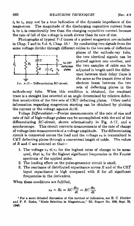
680 MEASURING TECHNIQUES [SEC. A.2
t, to t~,may not be a true indication of the dynamic impedance of themagnetron. The magnitude of the discharging capacitive current fromtsto t~ is considerably less than the charging capacitive current becausethe rate of fall of the voltage is much slower than its rate of rise.
Photographs of typical V-1 traces of a pulsed magnetron are includedin Chap. 7 and in Vol. 6, Chap. 16.1 By conducting two signals from thesame voltage divider through ditlerent cables to the two sets of deflection
‘Q=-—-.—-fc %
To CRTdeflection
R :+: c7s V~ plates
*FIG. A. 17.—Differentiating IK’-circuit.
plates of the cathode-ray tube,the two identical signals can beplotted against one another, andthe two samples of cable can beadjusted in length until the differ-ence between their delay times isthe same as the transit time of theelectron beam between the twosets of deflecting plates in the
cathode-ray tube. When this condition is obtained, the resultanttrace is a straight line oriented at an angle determined by relative deflec-tion sensitivities of the two sets of CRT deflecting plates. Other usefulinformation regarding magnetron starting can be obtained by plottingthe current or the voltage against dv/dt.
Voltage Diflerentiator. -Precise measurements of the rate of rise andrate of fall of high-voltage pulses can be accomplished with the aid of thedifferentiating RC-circuit, shown schematically in Fig. A. 17, and asynchroscope. This circuit converts measurements of the rate of changeof voltage into measurements of a voltage amplitude. The differentiatingcircuit is connected across the load and the voltage VRis transmitted toCRT deflecting plates through a convenient length of cable. The valuesof R and C’ are selected so that—
1. The voltage v, <<v c for the highest rates of change to be meas-ured, that is, for the highest significant frequencies in the Fourierspectrum of the applied pulse.
2. The loading effect on the pulse-generator circuit is small.3. The reactance of distributed capacitance across R and of the CRT
input capacitance is high compared with R for all significantfrequencies in the derivative.
When these conditions are fulfilled,
dv, ~ ~c q
“=Ri=Rcx dt
1For a more detailed discussionof this method of indication, eee R. C. Fletcherand F. F. Rieke, “Mode Selection in Magnetrons,” RL Report No. 809, Sept. 28,1945.

SEC. A*2] PULSE MEASUREMENTS 681
(a), (b). Voltage Pulwa and corresponding time derivative superimposed on the screenof a cathode-ray tube by the use of a mechanical commutator.
(c) Voltage pulse. (d) ‘lXme derivative of (c) obccrved withchort leads and matched cable.
(.) Time derivative of (c) observed with (f) Time derivative of (c) observed withshort leads and mismatched cable. long leads and mismatched cable.
Fm. A.18.—Voltagepulses and time derivatives.
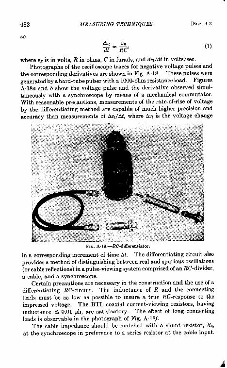
682 MEASURING TECHNIQUES [SEC. A.2
so@l=vndt EC’
(1)
where uuis in volts, Rin ohms, C in farads, anddu/dt involts/sec.Photographs of the oscilloscope traces for negative voltage pulses and
thecorresponding derivatives areshown in Fig. A”18. These pulses weregenerated byahard-tube pulserwith al~-ohm resistance load. FiguresA.18a and b show the voltage pulse and the derivative observed simul-taneously with a synchroscope by means of a mechanical commutator.With reasonable precautions, measurements of the rate-of-rise of voltageby the differentiating method are capable of much higher precision andaccuracy than measurements of Avz/At, where AVIis the voltage change
FIG. A.19.—RC-differentiator.
in a corresponding increment of time At. The differentiating circuit also
provides a method of distinguishing between real and spurious oscillations
(or cable reflections) in a pulse-viewing system comprised of an RC-divider,
a cable, and a synchroscope.
Certain precautions are necessary in the construction and the use of adifferentiating Rc-circuit. The inductance of R and the connectingIsads must be as low as possible to insure a true RC-response to theimpressed voltage. The BTL coaxial current-viewing resistors, havinginductance S 0.01 ph, are satisfactory. The effect of long connectingleads is observable in the photograph of Fig. A 18f.
The cable impedance should be matched with a shunt, resistor, Ro,at the synchroscope in preference to a series resistor at the cable input.

SEC. A.2] PULSE MEASUREMENTS
In this case R [Eq. (l)] should be replaced by R’ =
683
~O. If the cable
impedance is matched with a series resistor R~ at the cable input, anappreciable distortion that results from the time constant R~C, for thecharging of the synchroscope input capacitance may be introduced.Figures A. l& and f show the effect of improper cable-matching.
To eliminate high-frequency pickup by the low-voltage section, ashielded type of construction shouldbe used. A differentiator using anEimac VC12-32 vacuum condenserand a BTL coaxial noninductiveresistor is shown in Fig. A“ 19. Forqualitative observations in whichsome inaccuracy can be tolerated forthe sake of convenience, several ordi-nary carbon resistors ranging invalue from 25 ohms to 100 ohms maybe incorporated with a convenientswitching arrangement as in themodel made by Sylvania.
The input capacitance C, of thesynchroscope is effectively lumpedacross R, and must be below thelimits specified in the followinganalysis (see Fig. A. 17). This cwpacitance tends to bypass the higherfrequencies of the derivative v,, andtherefore C, should be made as smallas possible. The effect of c, on V.is indicated by an examination of theresponse to the leading portion of a
—
~hrT1 It,t
i,,
I,1
I~:
1 ,1
I,,,8
I ,!
r - tr- !#
---- Actual derivative— Vn(responee of differentiating
circuit, Fig. A 17) C =15 ~#f,R =50 ohms, Cs ’75 @Pf
FIO. A.20.—Hypotheticsd voltage pulseeand corresponding time derivatives.
(a) Trapezoidal voltage wave front.(b) Trapezoidal voltage wave front with a
spike.(c) Time derivative of (a).(d) Time derivative of (b).
trapezoidal voltage pulse applied to R1. It is assumed that the voltageimpressed on the clifferentiating circuit is of the form
where t, is the time of rise of the voltage pulse.For the time interval O s t s t,,
‘“=%[1-’-&’l(2)

684 MEASURING TECHNIQUES
where Cll = C + C., and for t2 t,
[SEC. A.2
‘,=?[l-e-k]’-=”Figure A%) shows a graph of the applied trapezoidal voltage wave
0.0500.045 , I I I I I I
-0.0200.015
0.010
0.005
I0102030 4O5OW7OZO9O1OQ
Cl, in WI
FIG. A.21 .—Graph for estimat-ing the maximum permissible valueof Cl] for k equal to one per cent.
front, its actual time derivative, and theresponse VR of a differentiating circuitwith typical parameters. Also plottedare a trapezoidal wave front with a spike,its corresponding derivative, and oR.
These hypothetical pulses and deriva-tives are plotted to demonstrate the typeof distortion that is caused by C. shuntingR. The time constant RC,l should beheld to a minimum for the best response ofthe differentiating circuit to suddenchanges in the impressed voltage.
From Eq. (2) a simple quantitativeexpression can be derived for determiningthe maximum permissible value of C1l forany desired fidelity of response to a linearly
rising voltage. For example, in order for UR/(RC) to be within 1 per centof dvJdt,
This relation requires that
t~ RCI, in 100and
t2 4.6RCH.
Figure A.21 is a graph of tversus C,, for various values of R. This
graph shows the time that is required after closing the switch for VR toapproach within one per cent of the true derivative, for any combinationof R and C1l. If greater tolerance in the accuracy of V.ispermitted, forexample, K per cent, the values of t are given by the product of
[’-Wand the corresponding values of tfor K = 1 per cent in Fig. A“21.
The photographs of Fig. A“22 show O.l-psec voltage pulses and thederivatives obtained with a resistance load and a magnetron load on ahard-tube pulser. The response of the differentiator to the spikes andto the small oscillations on the voltage pulses is observable in thesephotographs.

SEC. .4.2] PULSE MEASCREM ENTS 685
From the photographs of Fig. A. 18a and b, where the differentiatorresponse and the traces of the applied voltage pulse are superimposed,it might be inferred that the output voltage from the differentiator risesmore rnpidly than does the input voltage. This illusion appears becausen voltage divider was used to obtain the voltage-pulse trace; in this casethe divider ratio was about 150/1. Actually, the rate of change of the
(a) Voltage puke on resistance load.
(c) Time derivative of (a)
(b) Voltage pulse on magnetron load.
(d) Time derivative of (b).FIG. AZZ. -Oscilloscope traces of short pulses and their time derivatives. Sweep speed: 10
div = 0.2 ~sec.
voltage, vE, is less than that of the applied voltage, * is evident from the
differentiation of Eq. (2). Since C, is never zero, the value of dv,/dtis less than VJt, by the factor C/(C’ + C’.).
The calibration of an RC-differentiator may be accomplished by oneof the following three methods:
1. By the direct measurement of R and C. For many applicationsthe value of C is about 15 ppf or less. Accurate measurements ofsuch small capacitances are possible with a high-precision bridge,for example, the General Radio Twin-T, but elaborate precautions

686
2.
3.
.VEASUR1.VG 1’ECH.VIQIJES [SEC. A.2
must be observed and corrections must be made for lead inductanceand stray capacitance to ground resulting from the large physicalsize of the high-voltage condenser.Fly the measurement of AVLand At on a linearly rising portion of apulse, using an accurately calibrated high-speed sweep. Thevalues of Avl, At, and the corresponding UEmay be substitutedinto Eq. (l), to give
RC = ~.
Some modifications may be necessary in the pulse-generator circuitin order to obtain a linearly rising pulse that is suitable for calibra-tion purposes.By the removal of the resistor R and the substitution of a capac-itance C=. The unit can then be calibrated as. a capacitancedivider against a standard resistance divider under pulse con-ditions. The divider ratio thus determined is equal to
C+cz+c. +c.c
where C= can be chosen large so that C, and C,, the CRT inputcapacitance and cable capacitance respectively, constitute lessthan 10 per cent of the numerator. Then C. can be removed andmeasured easily on a bridge, and the values of C, and Cc eithermeasured or estimated. The value of C can then be calculatedwith a probable error no greater than the algebraic sum of theerrors in measurement of the divider ratio and of C. + C, + C,.This method of calibration is the most reliable.
Figure A.18b shows a linearly rising pulse on which an excellentcalibration check was obtained. The capacitance C of the differentiatorwas measured on a General Radio 821-A Twin-T precision bridge, withnecessary corrections for leads, capacitance to ground, etc. The averageof several readings was 13.3 t 0.2 WLf. A Wheatstone-bridge measure-ment of R’ gave 19.97 ohms as the parallel value of R and I?o. The verti-cal-deflection sensitivity on the CRT screen was 5.50 i- 0.05 volts per smalldivision. The voltage pulse was obtained from a capacitance divider witha ratio of 163/1, determined by comparison with a standard noninductive-resistance divider under pulse conditions. The estimated maximum errorof this calibration was i- 1 per cent. The CRT sweep calibration indi-cated by a 10-M c/see sine wave (tryst al-controlled oscillator) was
0.0208 ~ 0.004 Asec

SEC. A*3] PRACTICAL. CONSIDERATIONS 687
per small division. To determine Au/At, an enlarged photograph waamade of the oscilloscope trace, and a straightedge was laid along the linearportion of the leading edge of the voltage pulse. The slope of this linein divisions (the average of several readings) was 3.6. Hence,
* = 3,6
[
5.5 X 163At 0.0208 X 10⁻⁶ 1 = 155kv/psec.
Themaximum amplitudeo fuRwaso bservedt obe7.4&vkions. Bysubstituting into Eq. (1) there is obtained
dul 7.4 x 5.5x= 20 x 13.3 x 10–12
= 153kv/Psec.
A*3. Practical Considerations in Making Pulse Measurements.Puke Shape.-The number of pulse shapes actually encountered inpractical circuit work is legion and the irregularities in the shape of thepulses to be measured complicate the interpretation and specification ofmeasurements of both amplitude and Time—duration. A good oscilloscopic viewing
The ~F
system provides flexibility for instan-taneous or average amplitude measure-ments and qualitative information Zregarding the shape of a pulse.relatively slow rise and fall and the FIQ.A.23.—Sketchofanirregularly
shapedcurrentpulse.rounded corners of most pulses observedin practice are reproduced ~aithfully with pulse-viewing systems in whichthe design features of an ideal viewing system may only partially befulfilled. The problem of verifying the relation
1., = Tf,Il,
expressing conservation of charge, may be taken as an example of theimportance of pulse shape in the interpretation of the quantities involved.In this relation 1., is the average d-c current read by a meter in serieswith a rectifying load, 11 is the pulse current amplitude, r is the pulseduration, and j, is the number of pulses per second. In a circuit wherethe current pulse is of an irregular shape similar to that sketched in Fig.A% the fundamental question is how to measure, and 11 in order mosttruly to represent an equivalent rectangular pulse. In this particularcase such an equivalent pulse is any rectangular pulse whose area is equalto that of the irregularly shaped pulse. Although this definition of theequivalent pulse permits several values of lj and r, a commonly acceptedprocedure is to measure the amplitude of the average height of the pulse,corresponding to an imaginary line drawn through the top, and to takethe mdse duration at one half of this amplitude. This procedure satisfiea

688 hf EASURING TECHNIQUES [SEC. A.3
the law of conservation of charge, but when the peak instantaneous orpulse power, the total energy per pulse, and the r-f spectrum must allbe considered in determining an equivalent rectangular pulse, the problembecomes much more complicated (see Appendix B).
The irregularities in pulse shapes that are encountered make it appar-ent that the usefulness of metering circuits for determining pulse voltageor pulse current is limited to special applications where the shape isknown and the nature of the metering-circuit response to the particularpulse shape being measured is known. Measurements by meteringcircuits that are sensitive to pulse shape can properly be interpreted onlywith the aid of auxiliary oscilloscopic measurements, as discussed inSec. A3.
Shiekiing.-The importance of the shielding of all components of aviewing system cannot be overemphasized. Voltage dividers should beconstructed with the high-voltage section shielded from the low-voltagesection wherever feasible. In a capacitance divider or a differentiatoremploying an Eimac vacuum condenser, it is preferable to connect theouter sleeve rather than the inner cylinder of the condenser to the high-voltage terminal, in order that the corona path from this terminal willbe direct to ground and the inner cylinder will be shielded at low potentiaf.Often the r-f radiation produced by a sudden surge of current in onepart of a pulser circuit, such as when a magnetron starts to conduct,causes pickup on the deflecting plates of the cathode-ray tube, whichmay appear as high-frequency fuzz on the signal trace. It is sometimesvery difficult to distinguish between spurious oscillations or reflectionsin the viewing system, r-f pickup from a source of interference, and oscil-lations that really are present in the circuit being measured. In a syn-chroscope it is extremely important to shield the sweep circuit and allconnections to one set of deflecting plates from the other set of deflectingplates; otherwise, coupling between the circuits can cause “ crosstalk’!to appear on the signal. This crosstalk may appear as a steady backwardmotion of the sweep during the rise of the pulse, or it may appear as ato-and-fro oscillation of the sweep as the pulse rises or falls. Sometimes,even with the best shielding, it is necessary to add resistance suppressorsdirectly at the deflecting plates. The distributed capacitance is usuallyadequate for filtering if 1000-ohm noninductive resistors are inserted inseries with the plates.
Amplifiers.-In high-level work it is nearly always possible to obtainsufficient voltage amplitude for presentation of the signal directly ona CRT screen, and amplifiers are unnecessary. This is fortunate,because it is much easier to design and construct dividers with wide-band-transfer characteristics than to construct video amplifiers withadequate bandwidth.

SEC. A.3] PRACTICAL CONSIDERATIONS 689
Cable Properties and Delay Lines.—It is sometimes desirable to insertafixeddelay time inthesignal presentation, for example, when the CRTsweep is initiated or triggered by the same pulse that is to be viewed as asignal, that is, when self-synchronous operation is required. Whenusing a nonsynchronous pulser switch, such as a rotary spark gap, thesignal cannot be synchronized on the cathode-ray tube except by thismethod. Unless the signal can be delayed by a few tenths of a micro-second after the sweep is triggered and the intensifier pulse initiated,however, the leading edge of the pulse is lost to view. The photographsin Fig.appear
A.24a and b show a typical pulse on a resistance load as it wouldin ordinary synchronous operatiop with two different lengths of
(a) Synchronous operation, (c) Self-synchronous3 ft cable.
OWra-tion, 3 ft cable.
(b) Synchronous operation, (d) Self-synchronous oper~170 ft cable. tion, 170 ft cable.
l%+. A.24.—Photographs of voltage pulses showing the delay in the start of the sweepin self-synchronous operation, and the effect of a long 100-ohm cable on the observed pulseshape.
cable. The traces shown in Fig. A,24c and d are for self-synchronousoperation. It maybe observed that the cable attenuation is not constantwith frequency and that there is some distortion of the pulse. Thisdistortion is particularly noticeable in the rounding of the leading topcorner of the pulse and the slowing down of the rate of rise. There is alsoa slight decrease in the amplitude of the main part of the pulse that canbe corrected by measuring the attenuation factor for a particular sampleof cable, which is determined by the pulse amplitude at a point near thecenter of the top of the pulse. Usually, the attenuation factor for aO.l-psec pulse, when compared with the corresponding factor for longerpulses, shows greater losses for the shorter pulses. Lumped-parameterdelay networks that produce less rounding of the leading edge of a givenpulse, and that show less attenuation than a length of cable giving acorresponding delay time, have been designed and built, but the lumped
690 MEASURING TECHNIQUES [SEC. A .4
parameter networks usually introduce ripples and other irregularitiesbecause of the mismatch between sections. Unless the condensers areall carefully selected, the coils wound to very close tolerances, and thenetwork constructed with a relatively large number of sections, it. isusually preferable to have the greater, but smoother, distortion andattenuation produced by a cable, since there are fewer irregularities.
A.4. Voltage and Current Measurements inthe Charging Circuit ofaLine-type Pulser. Forward Charging Voltage.—In general, two types ofmeasurements are made on the charging-voltage waves in a line-typepulse-generator circuit. With a relatively slow CRT sweep and a high-impedance balanced parallel RC-divider, one or more complete cycles ofthe charging voltage may be observed for waveform and amplitudemeasurements. With an expanded sweep the voltage across the switchimmediately after the pulse discharge is observed to determine the magni-tude of post-pulse invense voltage across the switch or the pulse-formingnetwork, and the nature of its removal from the network during the earlyportion of the recharging period. These latter data are especially sig-nificant in the study of the circuit behavior of a line-type pulser usingd-c resonant charging and a unidirectional switch when the load imped-ance changes during a pulse or from pulse to pulse.
In measurements of charging voltage or inverse voltage, the timeresolution required is nearly always large compared with the transit timeof the short cables used with the dividers. The impedance-matchingproblem, therefore, becomes one of producing a balanced RC-dividerwhen the cable is treated as a lumped capacitance in the circuit. Con-sider, for example, a d-c resonant-charging circuit in which the maximumforward voltage on the puls~forming network is 8 kv and the averaged-c charging current is about 40 ma. These values correspond to a pulserecurrence frequency of 500 pps with a l-~sec 50-ohm network. To keepthe average current through the divider less than 1 per cent of thecharging current, its total d-c impedance must be at least 10 megohms.For a maximum signal of 80 volts at the CRT deflecting plates, the dividerratio should be about 100/1; therefore, the resistance of the low-voltagesection of the divider must be about 100,000 ohms. Let R2 = 105 ohmsand assume that Cc + C. = 75 ~~f. The time constant R2C, (Fig.A.3) is then equal to 7.5 psec. In order to form a balanced parallelRC-divider, the distributed capacitance across the high-voltage resistor,RI = 10 megohms, must be about 0.75 ppf. Since it is difficult to evalu-ate the distributed capacitance, it is better, in practice, to add a lumpedcapacitance of about 12 to 25 ppf, such as a high-voltage vacuum con-denser, in parallel with RI and then to increase Cz correspondingly.
During the charging period the loading effect on the pulser circuitproduced by this added capacitance (the sum of Cl and C9 in series) is

8EC. A.4] MEASUREMENTS IN THE CHARGING CIRCUIT 691
usually negligible, but during the pulse this capacitance dischargesthrough the pulser switch and, if Cl is comparable to the storage capac-itance of the pulse-forming network, the pulse current through theswitch at the beginning of the pulse is appreciably increased.
By using a string of carbon resistors in the “stove-pipe” shieldedarrangement shown in Fig. A“25, it is possible, without adding anyadditional capacitance and by using less thanthree feet of cable, to keep the effective timeconstant RIICII less than 5 psec. In this way anoscilloscopic presentation of the d-c resonant-charging voltage wave that is satisfactory for theobservation of the character of the general wave-form and for the measurement of the maximumforward-voltage amplitude is obtained, but thevoltage across the switch for a period of about 25psec after the pulse is not accurately reproduced.
Immediate P os t-p u ls e Voltage.—To makeprecise measurements of the post-pulse voltageacross the pulser switch (or pulse-forming nehwork) on an expanded time base, the followingtwo devices are used: a diode in series with aresistance divider, and an unbalanced RC-divider.For measurements of inverse post-pulse voltageonly, a diode is connected in series with a resist-ance divider as shown in Fig. A.26. The diodeprevents the current from flowing through theshunt path during the major portion of thecharging interval while forward voltage existsacross the pulser switch. The total resistancecan therefore be much less than is required fora balanced RC-divider with no diode. However,the resistance must be high enough to preventexcessive post-pulse inverse currents from flow-ing through the pulse-transformer primarywinding. Such inverse currents may influenceflux reset in the pulse-transformer core or cause
..JJ
FIG. A.25.—Resistance di-vider.
the inverse voltage on the pulse-forming network to discharge toorapidly. In a thyratron pulser employing a WI-ohm pulse-formingnetwork and a pulse transformer with a butt-joint core, a totalresistance of 2Q000 ohms or higher is usually satisfactory. Inversevoltage in a typical thyratron-pulser circuit may vary from a few hundredvolts during normal operation to nearly the same magnitude as the peakforward voltage during abnormal load conditions, such as magnetron

692 MEASURING TECHNIQUES
sparking. Hence, the desired divider ratios may
[SEC. A.5
vary from aboutiO/1 to-lOO/l or more. As an example, assume a divider ratio of 11/1.With R, = 20,000 ohms (including effective diode resistance), Rz shouldbe about 2000 ohms. If the total capacitance of the cable and CRT inputis 75 wf, the effective time constant, neglecting distributed capacitanceCl across RI, is
R,CS == 0.15 psec.
This value is tolerable for most measurements of post-pulse voltage.For precise measurements of post-pulse voltage of either polarity, anunbalanced RC-divider circuit, shown in Fig. A .27, is used with a syn-chroscope. These measurements, however, are only reliable for a fewmicroseconds after the pulse. The time constant R7.(CI + C’z) is made
m
‘&’ ‘3=. —FIG. A.26.—Resistance di- FI~. A.27.—Unbal-
vider used with diode for anced RC-divider formeasurements of post-pulse measurements of pOst-inverse voltage across the pulse voltages of eitherpulser switch. polarity across the pulser
switch.
long compared with the post-pulse interval of immediate interest, butshort compared with the entire interpulse charging interval. Hence,the waveform of the forward charging voltage is distorted considerably,and, at the instant before the switch breaks down, the voltage appearingacross Rz (and at the cathode-ray tube) is zero. The divider respondsas a capacitance divider that is reliable for a time short compared withthe time constant R*(C, + CJ. The reference potential for determiningwhether the post-pulse voltage is positive or negative is not the actualzero voltage on the CRT deflecting plates, but rather it is the flat por-tion of the signal occurring during the pulse. This voltage is not a truezero reference because it is in error by the 100- to 200-volt drop thatexists across the pulser switch during the pulse when it is in steady-stateconduction.
METERING TECHNIQUES
A*6. Pulse Voltmeters.-Several types of pulse-voltmeter circuitshave been designed in various laboratories both in this country andabroad. Included among the puls~voltage indicators that have been

SEC. A.5] PULSE VOLTMETERS 693
.
reportedl are balanced bridge circuits or feedback triode amplifiers usedin conjunction with high-voltage-input diodes or with resistance orcapacitance dividers, and at least one circuit based on an inverted-vacuum-tube principle. The discussion here, however, is confined to arelatively simple pulse-voltmeter circuit
=
that has proved reliable and widely adapti k’able in pulse-generator work at the Radi-ation Laboratory and elsewhere, and thatcan be calibrated directly on d-c voltage.The type of pulse voltmeter described here -is adaptable for measurements of approxi- Fx~.A.28.—Basicpulse-voltmeter
mately rectangular high-voltage pulsescircuit.
having amplitudes ranging up to 30 kv, durations greater than 0.1 psec,and recurrence frequencies greater than about 100 pps.
The basic circuit of the pulse voltmeter used at the Radiation Labora-tory is shown in Fig. A.28. The voltage of peak amplitude V1 to bemeasured is impressed between point P and ground. When the voltageat P is greater than the voltage VC at P’, the capacitance C charges upthrotigh the diode and V= rises. However, C discharges continuouslythrough R2, so Vc falls during the interval when the voltage atP is less than V.. With uniform regularly repeating pulses, Vc
approaches an equilibrium state in which the rise produced by the charg-ing through the diode is equal to the fall caused by the dischargingthrough Rz. When the parameters are suitably chosen, the averagepotential V. of C can be made very close to V~, with the result that V1 isgiven approximately by the product of Rz and the current indicated bythe microammeter.
The following analysis of the circuit leads to an expression for theintrinsic error of the pulse-voltmeter indication in terms of the circuitparameters and the duty ratio of the voltage pulses to be measured.With the aid of this error equation, meters can be designed to give theleast error for a particular operating condition. For example, when the
1The following references are typical but not all-inclusive:R. O. hlc Intosh and J. W. Coltman, “Negative Peak Volt meter,” Westinghouse
Rre.rarch Laboratories, Research Report No. SR-108, Nov. 12, 1941.“A Standard Voltmeter for Positive and Negative Pulses” U.S. Signal Corp
Technical Memorandum No. SPSGS-TRB-3, Mar. 23, 1944.E. C. S. Megaw, “ Recording Pulse Peak Voltmeter for Magnetron Flashing
Studies,” Genrml Electric Co., Ltd., Report No. S492, June 4, 1944.L. IJ. Hibbard, “ Pulse Peak Kilovoltmeter, ” R.P. 213, Commonwealth of Aus-
tralia, Council for Scientific and Industrial Research, Division of Radiophysics,Nov. 28, 1944.
R. Rudin, “Development in Peak Voltmeters and Ammeters for Use with PulsedMagnetrons,” BTL Report M M-44- 140-6S, Sept. 23, 1944.

694 MEASURING TECHNIQUES [SEC. A.;
duty ratio is 0.0002 or higher, parameters can be chosen such thatthe intrinsic error of the meter indication is less than two per cent.Practical design and operation problems are discussed, and a technique forviewing pulse-voltmeter operation is described.
The term “intrinsic error” is used throughout this discussion to meanthe inherently negative error resulting from the impossibility of chargingthe condenser completely to the voltage of the applied pulses. Thiserror is thus inherent in the circuit design, and is thus distinguished
1~1~. A.2’3—Equiva-hmt circuit for the Pulsevoltmeter of Fig. A.2S.
adequate means for
from practical errors produced by the change ofcomponents and the like. For example, errors of2 to 10 per cent have been observed that weredue to changes in the high resistance caused byheating from the nearby filament of the diode,and/or to inverse leakage current through thediode during theinterval between pulses. Apulsevoltmeter of this type, like most metering circuits,is sensitive to waveform, and measurements ofirregularly shaped pulses can be interpreted prop-erly only if the pulse voltmeter isusedinconjunc-tion with auxiliary filtering circuits and with
viewing both the applied voltage pulses and thepulse-voltmeter operation.
Analysis oj Intrinsic Error.-An analysis of the pulse-voltmeter cir-cuit can be made from the equivalent circuit shown in Fig. A29. Inthis circuit the diode is represented as a perfect rectifier in series with aresistance
RI =?,P
where VP is the tube drop corresponding to the plate current lP. Thecapacitance Cd, introduced to representthe diode capacitance, is first assumed L74 l-r-l l-r-lnegligible, and its effect on the pulse-voltmeter response is treated separately.It is further assumed that the voltagewaveform impressed on the pulse volt-meter consists of regularly spaced rectang- ‘m
ular pulses as shown in Fig. A.30, with FIG. A.30.—Idealized rectangular
T,>> ,. Also, the effect of the dischargevoltage waveform.
of the capacitance C through Rz is neglected in writing the equation forV. during the pulse.
The waveform of the current through the diode during the pulse isclosely approximated by a portion of an exponential charging curve as
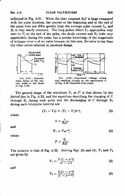
fhc. A-5] PULSE VOLTMETERS 695
indicated in Fig. A“31. When the time constant RIC is large comparedwith the pulse duration, the current at the beginning and at the end ofthe pulse does not differ greatly from the average pulse current 12, andR, is very nearly constant. For long pulses where Vc approaches verynear to VJ at the end of the pulse, the diode current and RI both varyappreciably during the pulse, but a precise knowledge of the magnitudeof intrinsic error is of no value because, in this case, the error is less thanthe other errors inherent in practical design.
Actualdiode
b
“ /currentwave
____ -- ~ Equivalent=, pulse = 1P,- 12
Ii
‘r
t-
Fr~. A.31 .—Approxi-mate shape of the cur-rent pulse in the diodeof Fig. A.28.
The general shape of
FIG. A.32.—Impreaeed voltage Pulseeand resulting voltage on the capacitance Cof Fig. A.29 (dietorted time scaIe).
the waveform V, at P’ is that shown bv thedotted line in Fig. A32, and the equations describing the chargin~ of Cthrough RI during each pulse and the discharging of C through Rzduring each interpulse interval are
(vi – v,) = (Vl – V,)tr”,
where
A = i%’and
VI = vze-~,
where
T=%.R,C
(3)
(4)
The notation is that of Fig. A-32. Solving Eqs. (3) and (4), VI and V,
are given by
VI = VJ1 – e-’)(5)eT _ e–A
and
v,= 1(’ ;_:::]. (6)

696
These equations may
and
MEASURING TECHNIQUES
be written
sinh $VI = V~e–~
s.h T + A’2
sinh ~V9 = V~e+~
sinh T + A“2
[SEC. A.5
(7)
(8)
Thus, if T is small (R.2C>> 2’,), both V, and VZ are nearly equal to V!,and the average value of VC is very close to HV1 + Vz).
The fractional intrinsic error, c,, in the meter reading is then givento a good approximation by
[ 1C.=+l(V1–LR2)=; VI–; (V2+V1) . (9)
If Eqs. (7) and (8) are substituted into this expression, the followingequation for e, in terms of the circuit parameters and the duty ratio isobtained:
sinh ~ cosh ~e,=l—
s.h (T + A;’
2
(lo)
which may be simplified to
When plotted as a function of C, C8varies in the manner indicated inFig. A.33. The minimum value of ~, is
‘“O=“m‘“=(’+$)-l‘(l+a-l” “2)c+ m
Evidently, best results at any given duty ratio can be obtained with themaximum values of C and of R2/R1. It is usually possible to choose R2greater than R, T,/r. Examination of the expression for c. reveals thatc, is then less than or approximately equal to 1.1 c.Oif C is greater thanT/Rl. Therefore, a simpler expression can be used for practical design

SEC. A.5] PULSE VOLTMETERS 697
and correction calculations, namely,
‘4‘(1+*)-’‘%) (13)
where
c>~ and TR~>> T,RI.
The difference between the value given by the right-hand member ofEq. (13) and the value given by Eq. (11) is less than or approximatelyequal to 0.1 (c. — c:).
It has been assumed in the above analysis that the capacitance ofthe diode has a negligible effect on pulse-voltmeter operation, which isequivalent to assuming that Cd/C is smallcompared with the fractional error in the
j:. \
meter reading. In some cases this is not true.
l--
Ass result of capacitance-divider action be- ‘.l%tween C and Cd, there are sudden approxi- ~ :&-
mately equal and opposite changes in VC at I c—the beginning and at the end of the period of -+,diode conduction. The true waveform of VC FIG. A.33.—The intrinsicis therefore not that shown by the dotted line error, c,, in the meter reading
as a function of the capaci-ln Fig. A .32, but that shown by the solid line. tance C.The magnitude of the voltage change pr~
duced by the capacitance-divider effect is CdV1/c, and for low duty ratiosthe fractional error in the voltmeter reading is increased to
(14)
where
c%and R2T >> T,RI.
If the voltage wave impressed on the pulse voltmeter has a backswingthat is appreciable in magnitude and duration, the error contribution ofthe capacitance-divider effect is increased slightly.
The procedure for evaluating c for a particular pulse-voltmeter read-ing, Va, is shown by the following calculation of the error in a typicalpulse voltmeter using a GL-8020 diode. If V. = 104 volts, R, = 500megohms, C,i = 6 y~f (including estimated circuit capacitance),T, = 2 X 10⁻³ see, ~ = 0.5 X 10⁻⁸ see, and C = 1000 ~Wf, the pulsecurrent through the diode is
1P =VOT,— = 0.080 amp.R,T

698 MEASURING TECHNIQUES
Thediode resistance Rl corresponding to this currentdiode-date characteristic (Fig. A”34) to be21200hms
[SEC. A.5
is found from theSince the condi- 1
tions i7> T/R, and Rm~>~,R, are satisfied, e is given by Eq. (14). \
(2) (lo-’) (2120) + 6(10-’2)‘= (5)(10’) (0.5) (10-’)
———— = 0.023 = 2.3 percent.10-9
The calculated and measured errors in typical pulse-voltmeter meas-urements are plotted in Fig. A“35 for various operating conditions. The ~
measured error was obtained by subtracting the pulse-voltmeter read-ings from those obtained with a synchro-scope and a capacitance divider. Thecapacitance divider was calibrated (withan estimated maximum error of +1 percent) against a standard resistance divider.The pulse-voltmeter was calibrated by ad-c voltage measured with a precision O-to
Plate voltagein volts
FIO-. A.34.—Plate-current—plate-voltage characteristic of type GL-8020diode.
1.O-ma meter and a standard 25-megohm
W-7 h
BGL 8020
cR2= 508 M
~ O-25rna
!:oc
Calcilletd.--/ error
------
10002OOO3OOO4OOORecurrencefrequencyin ppa
L~6\\ (a)
i;-
1000mmmRecurrencefrequencyin ppa
(b)FIG. A.35.—Puls+voltmeter er-
ror curves, (a) pulse duration:0.11 psec, C = 0.00115 pf, (b)pulse duration: 0.19 psec, C =0.05 pf.
multiplier. The high-voltage
source was connected to the point P’ of the pulse voltmeter in order toavoid any errors caused by the power-supply ripple and the rectifyingaction of the diode.
Design and Operation.—Praqtical design considerations dictate thatR2 be made as large as possible, consistent with the current meters avail-able. For measuring voltages up to 12,500 volts, it is convenient touse a O- to 25-pa meter with R2 = 500 megohms. For pulses from 0.1~sec to 2.0 psecs and duty ratios as low as 0.0002, the intrinsic error isless than 2 per cent for all values of C greater than 1000 ppf, providedthat the values of RI and cd for the diode are comparable to those forthe GL-8020. To extend the range up to 25,000 volts, a O- to 50-pameter may be used, or Rz may be made equal to 1000 megohms.
1

SEC. A-5] PULSE VOLTMETERS 699
Because of its high inverse-voltage rating (40 kv), the GL-8020 diodeis preferred to other diodes that may have a lower tube drop. TheWE-719A gave excellent results below 8 kv, but larger errors occurred at10 kv or higher because of inverse leakage currents. This tube also has alarger value of cd than the GL-8020.
PUseful qualitative information concerning
%$
P’
pulse-voltmeter operation can be obtained from c,a simple scheme for viewing the incremental
R2
voltage on C during the pulse. The single ~~~ c, R, wcapacitance C is replaced by two capacitancesin series, Cl and C2 (see Fig. A.36), the latter .
being shunted by a resistance RS of such valueFIG. A.36.—Pulse-volt-
meter with circuit for view-that the time constant RSCZis short compared ing the VOlta@ On thewith 2’,, but very long compared with r.
capacitanceC.
The synchroscope is connected across C2, and the voltage divider thuscreated presents a signal voltage
+ (v. – v,),‘“= C1+C2
which is a reasonably accurate representation of the incremental voltagewaveform on Cl when the diode is conducting. During the rise and fallof the applied voltage pulse, when the diode is not conducting, the signalis influenced by the capacitance cd of the diode which, together with Cland Cz, acts as another voltage divider. In practice, the applied pulse isusually more nearly trapezoidal than rectangular in form, and typicalsignals appear as shown in the photographs in Fig. A“37. The curvatureof the signal is a qualitative indication of the degree to which V2approachesVz during the pulse, and the amplitude is an indication of the loss ofvoltage on Cl during the interval between pulses. The incrementalvoltage signal becomes nearly flat on top if Vz approaches very near toVj.
For example, in Fig. A.37 trace a is the 0.25-psec pulse (measured atthe top) that was impressed on the pulse voltmeter. Traces b, c, and dindicate the effect of successively increasing recurrence frequencies,showing correspondingly decreasing errors. Traces b, f, and j show acomparison of the incremental voltages for a recurrence frequency of500 pps with pulse durations increasing from 0.25 to 1.0 psec. As thepulse duration increases, the signal becomes successively flatter, whichshows a decreasing error in the meter indication.
An undesirable spike or, in some cases, high-frequency oscillationsmay be present on the leading edge of the voltage pulse that is to bemeasured. Such transients tend to cause the pulse-voltmeter readingto be too high, unless some form of filtering is employed. A simple

700 MEASURING TECHNIQUES [SEC. A .5
remedy is to insert anextra resistance inseries with the lead between thediode and the source of pulse voltage. The RC-filter comprised of this“ despiking” resistor and the total capacitance to ground (capacitanceC, of the high-voltage-lead and the diode-plate connector added to theseries value of cd, cl, and C2) is very effective. However, great care
(a) 0.25 psec voltage (b) 525 ppe. (c) 1000 pps. (d) 2000pps.pulse. Incrementalcondenservoltage.
(a) 1 psec voltage pulse. O) 525 ppt% (k) 1000 pps.Incremental c0nden8er voltage.
FIG. A.37.—Negative voltage pulses impressed on a pulse voltmeter and the correspond-ing incremental voltages at various pulse durations and recurrence frequencies. Theincremental voltage is shown by the trace between points (A) and (B).
must be taken to insert only the minimum additional resistance requiredfor filtering, because any increase in R, raises the intrinsic error of thepulse voltmeter. It is helpful to employ the previously mentioned view-ing scheme to insure that RI is not increased too much by the addition ofthe series despiking resistor. To ascertain whether or not the filteredpulse is “clean,” a capacitance divider may be connected across the pulsevoltmeter, as indicated in Fig. A.38, and the signal viewed on the screen

SEC. A .6] THE AVERAGE-CURRENT METER 701
of acathode-ray tube. Figure A.39shows arepresentative pulse beforeand after filtering.
It must be noted that this divider actually becomes a part of thefilter and, if it is removed after serving its viewing purpose, it should be
FIG. A.3S.—Complete schematic dA-gram of diode pulse-voltmeter circuit,including despiking flter.
replaced by an equivalent capaci-tance. In some cases, it may provemore expedient to add a small amountof capacitance to ground in order toincrease the filtering rather than to
l-mFIG. A.39.—Representa-
tive pulse before and afterfltering.
add more resistance. This practice also requires caution against loadingthe circuit whose voltage is being measured. When the diode is reversedfor reading negative pulses, the capacitance of the filament transformerbecomes a part of the filter.
A.6. The Average-current Meter.—Theobvious simple expedient for measuring aver-age current in a pulse circuit is to connect aconventional current meter of suitable rangein parallel with a large capacitance. Themagnitude of the capacitance required isdetermined by the internal impedance of thepulse generator, the pulse duration, the volt-age-current characteristic of the load throughwhich the pulse current flows, and certainphysical properties of the meter. To guardagainst disturbance of the pulse-generatorcircuit by an average-current-metering circuitthat is connected in series with a nonlinearload, either the static or the dynamic imped-ance of the load (whichever is smaller) must beconsidered. In practice, it is sometimes ad-visable to insert additional resistance and/orinductance in series with the meter as a furtherprotection against surges of current that mayinjure it. A resistor is usually connected inground the load in case of meter burnout.
~—FIG. A.40.—Schematic dia-
gram of pulse-discharging cir-cuit including the equivalentcircuit for a magnetron and an
average-current meter.
shunt with the meter to
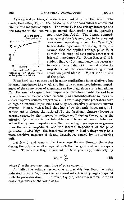
702 MEASURING TECHNIQUES [SEC. A .6
As atypical problem, consider thecircuit shown in Fig. A40. Thediode, the battery V,, and the resistor r-lform the conventional equivalentcircuit fora magnetron input. Thevalue V,isthe voltage intercept ofaline tangent to the load voltage-current characteristic at the operating
point (see Fig. A.41). Thedynarnic imped-
: -:*
L
ante rl = AVZ/AZl is assumed to be constantover a small operating range. Let R1 = Vt/11
be the static impedance of the magnetron, and
Is ‘“ : assume that the applied voltage pulse V1 of,’ I duration r is supplied by a pulse generator of% I
g I internal impedance Ra. From Fig. A.41 it isgevident that rl < Rl, and hence it is necessary
“o Current— I to determine a value of C that will make the
FIG. A,41.—Magnetron impedance of the current-metering circuitvoltage-currentcharacteristic small compared with ri + Rc for the durationunderpulseconditions. of the pulse.
Most hard-tube pulsers used in radar applications have relatively lowinternal impedances (h% = rl), and line-type pulsers have internal imped-ances of the same order of magnitude as the magnetron static impedanceRI. For small changes in load impedance, therefore, hard-tube and line-type pulsers can be considered essentially as constant-voltage sources andconstant-power sources, respectively. Few, if any, pulse generators haveso high an internal impedance that they are effectively constant-currentsources. Hence, with a load that has a low dynamic impedance, it isconvenient to choose the ratio AI[/1~, the fractional change (droop) incurrent caused by the increase in voltage on C during the pulse, as thecriterion for the maximum tolerable disturbance of circuit behavior.When the dynamic impedance of the load is high, perhaps even greaterthan the static impedance, and the internal impedance of the pulsegenerator is also high, the fractional change in load voltage may be amore sensitive measure of circuit disturbance caused by the meteringunit.
Let L = O, and assume that the charge flowing through the meterduring the pulse is small compared with the charge stored in the capac-itance. Then the voltage increment on C is given approximately by
(15)
where Z1is the average magnitude of pulse current.Actually, the voltage rise on C is appreciably less than the value
indicated in ?3{4.(1.5), unless the time constant r~C is very large comparedwith the pulse duration T. However, Eq. (15) leads to a safe value for all
cases, regardless of the value of r~.

SEC.A.6] THE AVERAGE-CURRENT METER 703
If a constant pulser voltage V1 is assumed, the decrease in load cur-rent caused by the voltage increment AuCis
and, combining Eqs. (15) and (16),
If the metering circuit is permitted to cause a
(16)
(17)
1 per cent change (droop)in the current, the minimum value of C’ is given by
c 1007=—rl + RGJ
(18)
As an example, let 7 = 10-6 see, n = 100 ohms, and RQ = 150 ohms.Then C’ must be at least 0.4 pf in order to insure that the ratio AIJIl isless than 0.01. The value of R, is not critical, but should be very largecompared with r~, unless the meter and shunt are calibrated togetheron direct current.
Although a value of C determined by Eq. (16) satisfies the criterion forthe disturbance of the circuit behavior, it is also necessary to considerwhether a capacitance of this value is sufficient to protect the meteradequately. The peak surge current through the meter during normaloperation of pulser and load is
1. = It (1 – e-fit), (19)
whereas the average value of direct current indicated by the meter is
1.. = IITj,, (20)
where f, is the pulse recurrence frequency. The ratio sIJI.. is a measureof the overload imposed on the meter, where s is the fraction of the full-scale deflection indicated by the meter when it reads 1.,, and is given by
-L
s=p(l-e’”~ (21).. ?f r
For example, if r~ = 10 ohms, C = 0.4 ~f, r = 1.0 psec, j, = 1000 pps,and the meter indicates a half-scale deflection, the calculated value of S’ isabout 110. Although manufacturers’ ratings generally do not includespecifications of this surge ratio, experience has shown that it is advisableto keep the ratio considerably lower than 100. The magnitude of Smay be lowered either by choosing a capacitance that is several timeslarger than the minimum value given by Eq. (18), or by adding a resist-ance in series with the meter to increase the effective value of r~. Several

704 MEASURING TECHNIQUES [S~cA6
current meters in common use with scales up to 15 ma, 25 ma, or 50 magave measured values of r~ ranging from 25 ohms to 2 ohms. The“thermal inertia” of the winding and the mechanical inertia of the move-ment of most conventional millimeters are appreciable, and surge ratiosup to about 50 seem to be reasonably safe at short pulse durations of theorder of magnitude of a microsecond or less. However, for long pulses ordelicate meters, a surge ratio of 50 may be too high.
The quality of paper or electrolytic condensers used for high capac-itances may be somewhat questionable. Consequently, to insure goodhigh-frequency response to pulses with steep wavefronts, a second smallcapacitance of high quality, usually mica or silver ceramic, is sometimesconnected in parallel with the larger condenser.
The use of an inductance in series with the meter should not be neces-sary during normal operation of a pulse generator with a stable load.In certain cases, however, instability of the load, for example, magnetronsparking, may result in abnormally large unpredictable surges of current.With a hard-tube pulser, the current during a magnetron spark is limitedonly by the emission of the pulser switch tube; occasional] y the switchtube sparks also, allowing the current to become many times the normalvalue. In such cases an inductance is inserted in the metering circuit asshown in Fig. A.40 to provide added protection for the meter. To beeffective, the time constant L/r_ should be large compared with the pulseduration. The values of r~ and R, also should be chosen properly inorder to prevent post-pulse oscillations in the meter circuit. To satisfythese conditions it may not be possible to make R, >> r~. Hence, theentire unit should be calibrated on direct current.
A magnetron or an equivalent rectifying load does not conductappreciably in either direction when the voltage across it is less than athreshold value V, (see Fig. A.41). Therefore, since the voltage VCon Cis always small compared with V,, the metering circuit may be isolatedfor an analysis to determine the conditions which must be fulfilled toprevent post-pulse oscillations.
The part of the circuit comprising C, r~, L, and R, of Fig. A.40 maybe analyzed in the same manner as that used for the circuit of Fig. 2.22.In the latter case the Laplace-transform equation for the voltage acrossthe shunt condenser was shown to be given by Eq. (236) and from thisequation the condition for oscillation is determined. In the present caseit is of interest to determine the value of R, associated with the meter inFig. A.40 which will make the circuit critically damped. This value ofR, must satisfy Condition 2 of Eq. (2.43), namely,
b=az (243)
where a and b are given by Eqs. (2.38) and (2.39) and in the notation of

SEC. A.6] THE AVERAGE-CURRENT METER 705
Fig. A40thesebecome,1
~=;+cc’ (22)
and
~+~”b=LC R&C
(23)
From Eqs. (22), (23), and Condition (2”43)there is obtained,
(24)
There are now two cases of interest depending on the value of r~ relativeto 2 4L/C.
Case l... rm<2~C
Under this condition oscillations in the loop containing C, r~, and L
are possible for R, = @, a familiar circumstance. Equation (24) givesone positive value and one negative value for R.. The negative valuehas no significance in this problem for obvious reasons, and the positivevalue determines the only condition for critical damping. Any value ofR, less than this positive value will insure overdamping in this case.
When this condition is satisfied the circuit is aperiodic with R. = ~.
However, Eq. (24) reveals the interesting fact that R. has two positivevalues when r~ > 2 GC, and hence that the circuit is criticallydamped for two values of R,. Oscillation is possible for any R, betweenthe two critical values. When the time constants L/r~ = R.C, thecircuit oscillates with its minimum period T = % ~.
In designing a meter protective circuit where the values of C, r~, and L
have been chosen in accordance with Case 2, it is advisable to make R,
larger than the greater value determined by Eq. (24). In fact, R. canbe chosen large enough to obviate the necessity of calibrating the circuitas a whole.
To illustrate the above considerations two numerical examples aregiven:
1. Let L = 1 mh, C = 2 pf, and r- = 15 ohms. Substituting thesevalues into Eq. (24), the values of R. are found to be,
R, = 500/(15 t 10 ~~)= 13.4 or –67.8 ohms.
Thk example comes under Case 1 and the circuit is aperiodic for anyvalue of R, less than 13.4 ohms. The negative value is disregarded.

706 MEASURING TECHNIQUES
2. Using the same values of L and C, let r~ =
Thisthan
two values of R, are
R, = 500/(25 + 10@= 10.6 or 189 ohms.
example is representative of Case 2. Any
[SEC. A*7
25 ohms. Then the
value of R, greater189 ohms or less than 10.6 ohms will insure adequate damping,
but the practical matter of calibration suggests a preferred value ofR,>> 25 ohms. Note that L/r~ = 40 psec, which indicates that themeter-current surge ratio is now reduced to less than 3 per cent of theratio that exists when L is negligible in the circuit.
The principles outlined in this section have been written for a metercircuit connected directly in series with a pulse-generator load that actsaa a rectifier. In some applications, it may be more convenient to con-nect the metering unit in some other position, for example, in series with apulse transformer. When this is done, there is one further precautionthat should be observed. There must be a proper rectifying element inseries with the meter to eliminate the errors caused by interpulse currentsthat recharge either the stray capacitance or the pulse-generator storagecondenser, and that have a net flow in the direction opposite to the pulsecurrent. Another alternative is to connect the average-current meterinto the pulse-generator circuit in such a way that only the charging cur-rent is measured. When the meter is thus isolated from the pulse cur-rent, the problem of meter protection is simplified, but the meter readingmay not be a reliable indication of the actual load current because ofshunt losses produced by the stray capacitance in the pulse-generatordischarging circuit.
A.7. Auxiliary Measuring Techniques.-R-f Envelope Viewer and
Spectrum Analyzer.—There are two methods that are most commonlyused for examining the r-f pulse-voltage envelope. One method is toconnect an r-f probe through a voltage divider to a square-law detector,and to feed the rectified voltage through a suitable video ampli6er to theplates of the cathode-ray tube in a synchroscope.
The other method is to feed a relatively large portion of the r-f powerinto a lighthouse cavity detectorl and to present the output rectifiedvoltage directly on the plates of the cathode-ray tube of a synchroscope.This method is superior for precision laboratory measurements becauseno video amplifier is required, and because the response can be madereasonably good for frequencies up to about 50 Me/see as the bandwidthis determined chiefly by the resonant Q of the cavity and the distributedcapacitance.
1P. A. Cole, J. B. H. Kuper, and K. R. More, “Lighthouse R.P. Envelope Indi-cator,” RL Report No. 542, Apr. 7, 1944.

SEC. A .V AUXILIARY MEASURING TECHNIQUES 707
The type of spectrum analyzer developed at the Radiation Laboratoryconsists essentially of a narrow-band receiver with a square-law detector,an audio-frequency sawtooth-voltage source that frequency modulatesthe local oscillator and supplies the CRT sweep, and an oscilloscope.The local oscillator is of the cavity reflector type (usually a Klystron, aMcNally tube, or a Shepherd tube) and has an approximately linearfrequency response as a function of reflector voltage. The r-f power issupplied from a directional coupler or probe in the waveguide output ofa magnetron (or other oscillator) through a suitable voltage divider. Asthe local-oscillator frequency varies, the CRT spot moves across thescreen, and the power received during successive pulses causes the spot totrace a line-amplitude spectrum. Actually, this spectrum is very nearlythe absolute value of the power spectrum. For pulses of duration shorterthan 2 psec, an r-f bandwidth of 10 kc/see in the receiver of the spectrumanalyzer is satisfactory. To obtain the best results with .$psec pulses, aconsiderably narrower band is required.’
A spectmm analyzer is used to determine whether or not pulses thatdroop, or are otherwise irregular in shape, cause serious frequency modula-tion of a pulsed oscillator. It is also used to measure the effective pulseduration, since the r-f bandwidth measured between pairs of minima onthe spectrum is inversely proportional to the pulse duration of the cur-rent and the r-f envelope (see Appendix B). This application is especiallyimportant when very short pulse durations of less than 0.1 psec are used,where it is difficult to produce good pulse shapes and to obtain reliablemeasurements of pulse duration with a linear time base, but where thewidth of the significant part of the r-f spectrum is greater than 10 Me/see.
Impulse Counting. —When abnormal load behavior, such as magnetronsparking, causes random pulse currents of abnormally high amplitude in apulse-generator circuit, it is sometimes desirable to count the recurrencesof all pulses having amplitudes exceeding a predetermined value. Conv-entional scaling circuits with minor circuit modifications and special
I For a detailed description of such a spectrum analyzer and operating instructions,see the instruction manual, “Spectrum Analyzer (Type 103) for Pulsed Oscillators at3,000 Me/see,” RL Report No. M-115, Nov. 18, 1942.
Criteria for evaluating pufze spectra for magnetrons are discussed in the followingreporta:
R. T. Young, Jr., “Fourier Analysis of pokes with Frequency Shifts During thePrdee,” RL Report No. 52-5, Jan. 30, 1943.
R. T. Young, Jr., “Frequency and Spectrum Characteristics of Standard Mngne.trons and the Effect of Change of Shape of Current Pulse,” RL Report No. 526, Mar.12, 1943.
G. N. Glaaoe, “Pulse Shapes and RF Spectra for Combinations of Stronlbrr&Cadson Mark I and Mark II Modulators with 2J22, 2J21, and 725A Magnet rons,’’RJ,Report No. 518, Mar. 17, 1944.

708 MEASURING TECHNIQUES [SEC. A7
shielding have been adapted for recording pulses of durations up to 5 psecat recurrence frequencies of less than 1000 pps.
---
}l&k ;$ ‘I ~ 5R2.
0.005 , “l\2M “160k-
1 !-(
2.2k_!!zl 1 ‘
6AL5
*“ & =N?
150
470 k15 Jq4f~f --- ---
FIG. A.42.—Schematic diagram of a spark counter showing the input and the first stage
FIG. A.43.—Records of average magnetron current ehowing sparking as a function of time.
For counting magnetron sparks, it was found advisable to provide abias threshold adjustment on the input stage. A “pulse-stretching”circuit was introduced at the output of the first diode to insure uniformsensitivity of the counter for pulse durations from about 0.1 psec to 5 psec.It was also necessary to insert a pulse-amplitude limiter at the input of the

SEC. A 7] AUXILIARY iilllASl ‘RING TECHNIQUES 709
first scaling stage in order to prevent the second stage from being trippeddirectly by pulses of high amplitude at the first stage. The input cir-cuits and one stage of a typical scaling circuit are shown in Fig. A“42.The output of the last stage is usually connected to an electromechanicalcounter.
For indicating bursts of sparking recorded over longer periods of timea recording millimeter is useful. Two sample records are shown onFig. A.43. On the upper strip the tape was run at high speed, and theapproximate numbers of individual sparks per indicated burst are printednear the current peaks on the record. The tape was moving from rightto left and the current amplitude increased downward. On the lowerrecord, the tape was running much more slowly, as indicated, and therate of sparking became excessive as the magnetron approached the endof life. The bursts of sparking usually cause increases in current (down-ward), but there is evidence of magnetron mode-changing with occasionaldecreases in current (upward peaks), especially during the last hour oflife. The n-,arlis along the lower border of the tape were produced byconnecting a second recording pen to the output of the electromechanicalcounter on a scale-of-16 pulse counter to indicate every 1600 sparks ofthe magnetron.

APPENDIX B
PULSE DURATION AND AMPLITUDE
BY W. H. BOSTICK AND J. V. LEBACQZ
IAmong 11,e most important parameters in the rating of pulse genera-
tors are pulst: amplitude and pulse duration. In Chap. 1 it is stated thata pulse is the departure of some electrical quantity—voltage, current orpower-from zero or from some equilibrium value. In general, the pulseis repeated at regular intervals, and for all practical considerations, thepulse duration is very short compared with the interpulse interval.There are a few exceptions, such as the “coded” pulses, in which a seriesof short pul~es have a short time interval between them, but the code isrepeated at relatively long time intervals.
Pulseduration
1
Pulseduration
h IYW L
r 7Pulse
amplitude
(a) (b)
(a) Ideal step-function (b) Actuai pulse and equ; v-pulse. alent ideal pulse; departure
areas are shaded.F~o. B.1.—Pulse shapes.
The concepts of pulse duration and pulse amplitude are very straight-forward in the case of an ideal step-function pulse (Fig. B. la); there canbe no ambiguity in the definition of either, since the variable changesinstantaneously from zero to a constant value that is the pulse amplitudeand, after a time ~ (the pulse duration) returns instantaneously to a valueof zero. In practice, unfortunately, an ideal step-function pulse cannotbe realized, and the value of pulse duration becomes indeterminate with-out an adequate definition. Since most pulsers have been designed toproduce a pulse that approximates as ciosely as possible a step-function orrectangular pulse shape, it is only natural that, in the consideration ofpractical pulses, most of the definitions of pulse duration and pulseamplitude are in terms of an equivalent rectangular pulse.
There have been many attempts at definitions, and the problem iscomplicated by the fact that pulser loads can be either pure resistances oroscillators whose characteristics approximate those of a biased diode.
7!9

SEC. El] EQUIVALENT RECTANGULAR PULSE 711
For instance, the pulse duration on a magnetron load has been variouslydefined as the duration of the voltage pulse at 90 per cent of the averagemaximum voltage amplitude, or as the duration of the current pulse at50 per cent of the average maximum current amplitude. These defini-tions may be satisfactory in some cases, but the “average maximum cur-rent amplitude” of a current pulse that is in the general form of a half sinewave, for example, is meaningless.
The purpose of this appendix is to discuss several methods for deter-mining average pulse amplitude and pulse duration that are based onequivalence of some quantities of the actual pulse and those of an assumedrectangular pulse. From the point of view of pulser output alone, themost important quantities are charge and energy; hence, an equivalentrectangular pulse constructed on the basis of equal charg~or averagecurrent—and equal energy per pulse can be used to define the pulseamplitude and duration.
In radar applications, however, one criterion of satisfactory operationof the transmitter is general] y the width of the r-f spectrum. Since, fora rectangular pulse, there is a definite relationship between the pulseduration and the spectmm width at one-half power, the duration of arectangular pulse equivalent to any actual pulse shape can be determinedby r-f spectrum considerations. The second section of this appendixconsiders the possibility of the use of spectmm equivalence in determiningpulse duration.
The equivalent rectangular pulses determined for a given pulse shapeby different types of equivalence are not the same; the more nearly theactual pulse shape approximates a rectangular pulse, the more nearlyequal are the values of pulse duration and amplitude obtained by thediflerent methods of equivalence. If the dilTerence in the results obtainedby the diRerent methods is appreciable, the choice of the definition isdetermined by considering the particular purpose for which the definitionis being used.
B.1. Equivalent Rectangular Pulse by Conservation of Charge andEnergy.-The general case of a load that can be represented by a biaseddiode is represented in Fig. B*2. If a current i(t) flows in the load, theinstantaneous power absorbed by the load is given by
PI(O= w, + ?lil(t)]il(t). (1)
If only one pulse is assumed to be applied to this load, the equivalentrectangular pulse of current 11, power Pz, and duration r, is defined by anequation, for the conservation of energy,
\
.Prr = pi(t) dt
-.(2)

712 PULSE DURATION AND AMPLITUDE [SEC. B.1
and an equation for conservation of charge,
!.
Ilr = i(t)dt, (3)—.
and by the load relation in Eq. (1), which is assumed to be valid for any
(a) Equivalent circuit. (b) Voltage-current characteristics.FIG. B.2.—Biased-diode load for pulser.
value of current. The equivalent pulse voltage is then
PZ
‘z = Tt”
If the instantaneous power can be written
p,(t)= Plf(t)
and is zero at any time except when O < t < ra, Eq. (2) becomes
(4)
Of course, Pl and 11 are not yet known, but they can be obtained bysolving Eqs. (1), (2), and (3). Also, as it is asaumed that Eq. (1) isvalid for any value of current,
or
,,=.g,J~
Similarly,
ii(t) = – : +J( )
; ‘ + +f(t).
If these values are introduced in Eq. (3),

SEC.B.1] EQUIVALENT RECTANGULAR PULSE 713
Equations (6) and (4) each separately determine the pulse duration 7 as afunction of the assumed equivalent pulse power PI; hence, after theintegrations have been performed, values for r and Pl can be obtainedalgebraically by solving Eqs. (4) and (6) simultaneously. For a pure-resistance load V. = O, and Eq. (5) becomes
(7)
The above method of uniquely determining r and Pl breaks down ifthe load resistance n becomes zero, for then Eqs. (2) and (3) are identical,and any pulse duration can satisfy the conditions of equivalence of energyand charge. This lack of uniqueness when n = O is a disadvantage ofthe foregoing method because most magnetrons have a small value of n,and the resulting power pulse is not very different from the current pulse.AS a result, great care must be taken to obtain satisfactory accuracy inthe determination of r.
Three examples of the use of the above method are now given: thepulse duration and amplitude of a triangular and of a sinusoidal powerpulse are given first, and a practical application to the determination ofequivalent rectangular pulses of actual magnetron load pulse shapesfollows.
Triangular Power Pulse on a Pure-rm”stance Load.-The instantaneouspower during the first half of the pulse of Fig. B.3 is given by
=“”;;MO = ~a
hence,
j(t) = g t.
If j(t) is introduced in Eq. (4),
If the two expressions for pulse duration are equated,

1714
or
and
PULSE DURATION AND AMPLITUDE [SEC. B.1
J_Pm 2 Pm
2Pl = 5 7;’
Pl = &Pm
T = +..
Sinusoidal Power Pulse on a Pure-resistance Load.-The expression forinstantaneous power for the pulse of Fig. B*4 is
Hence
pi(t) = Pm sin ~.
FIG. B.3.—Triangular powerpulse.
FIG. B.4.—Sine-wave powerpulse.
The relations between the duration and amplitude of the equivalentrectangular pulse on a resistance load can again be obtained from Eqs.(4) and (7)
/
s.@ dt= Pm 2,.,
‘=iF&::t= ‘~%%”
By equating these expressions for pulse duration, the relationship
PmPl=— (~.~g’)z = 0-7p-
is obtained. Then2 10.T= (1.194 )z–rc = —7~.u 11
Pulses on Jfagnetron and Re&istance Loads.-The above method per-mits the determination of the equivalent rectangular pulse for any pulseproduced by an actual pulse-forming network. As typical examples,consider the voltage and current pulse shape, and the power pulse shape

SEC. El] EQUIVALENT RECTANGULAR PULSE 715
(a)
(b)
(c)
[&
(e)l%. B.S.—Voltage, current, and com-
puted power pukes in an HK7 magnetron,(a) with a l-ccction pulw+forming network,(b) with a%wctionp uls~formingn etwork,(c) with a 3-ccction puls-forming net-work, (d) with a 4-cection pub-formingnetwork, (e) with a 6eection puke-formingnetwork.
(a)
(b)
(c)
(d)
(e)
Fm. B.6.-Current and computedpower pufces on rcsiatancc load, (a) with al-ccction pulce-forming network, (b) witha Z-cection pulse-forming network, (c)with a 3-cection puke-forming network,(d), with a 4-eection puke-forming network,and (e) with a &action p~forxningnetwork.

716 PULSE DURATION AND AMPLITUDE [SEC. B.2
obtained by calculation of the product of instantaneous observed pulsevoltage and instantaneous observed pulse current shown in Fig. B.5 forone-, two-, three-, four-, and five-section networks operating into amagnetron load. The values of r, 11 and PI have been calculated foreach case as follows, the only assumption being that the current is asingle-valued function of voltage. First, the integrations indicated inEqs. (2) and (3) are performed graphically. Then the ratio
is calculated. The value of 11 corresponding to this value of VI may beobtained by finding a point on the voltage pulse at which the instantane-ous voltage is equal to this value, and determining the value of instantane-ous current at that instant from the corresponding current pulse. Withthe values of V1 and Zl known, the values of T and P1 may be calculatedreadily. The equivalent rectangles thus determined are indicated inthe Fig. B.5. All equivalent rectangles are so placed on the diagramsthat a vertical line bisecting the rectangles will also bisect the area ofthe actual pulse shape.
Similar calculations have been carried through for the pulses producedon a pure-resistance load by the same networks. Instantaneous currentand power pulse shapes, the latter obtained by squaring the instantaneouscurrent, and the resulting equivalent rectangles, are shown in Fig. B6.
B-2. Equivalent Rectangdar Pulse by Minimum Departure Areas.—The method of minimum departure area is an attempt to predetermine an
~b~
Fm. B.7.—D+termination of min-imum departureareas for a triangu-lar puke.
equivalent rectangular pulse that has the same energyas the actual pulse and produces a spectrum distribu-tion equal to that of the actual pulse over the mostsignificant part of the spectmm, that is, down to atleast the half-power point.
For simple pulse shapes, it can be shown that thespectrum distribution satisfies the above requirementif the rectangular pulse chosen is that for which thesum of the “departure areas” (see Fig. B. 1b) is a min-imum. The assumption is then made that, for anypulse shape obtained in practice, the rectangular pulse
giving equality of energy and leading to the minimum total departure areaalso gives a frequency spectrum equal to that of the actual pulse over themost significant portion of the spectrum.
If one half of a symmetrical triangular power pulse (Fig. B.7) ofmaximum amplitude a and duration 2b at the base, and the equivalentrectangular pulse of amplitude h and duration 2C are considered, thecondition of equal energy provides the relation

SEC, B.2] EQUIVALENT RECTANGULAR PULSE 717
ab— = Ch.2
The sum of the departure areas is given by
[A=; ~(a–h)’+~(b– c)’+ 1
(UC– ab + bh)’ .
ab(9)
If the value c = (ah)/(2h) is introduced in Eq. (9) and the terms arerearranged,
By differentiating with respect to h and equating to zero, the values of hfor which the area is a minimum are obtained. Thus
$= W[4(Y-4(:Y+2:-’1 =’Jand
‘(:) -’(:) +”2(:)-1=”
which can be rewritten
[2(:) -2(2+11[2(:) -11=0and the solutions are
h
i ‘*&’and
h 1+<–1.=a 2’
obviously, only the real positive root is of interest in the discussion, or
h- = 0.707.a
Figure 13.8shows the calculated frequency spectrum for a symmetricaltriangular pulse, and the theoretical spectra for several rectangular pulsesof equal total energy, but of different ratios of amplitude to duration.It can readily he seen that the spectrum for the triangular pulse is super-imposed on that of the rectangular pulse that has an amplitude 0.707times that of the triangle from the maximum down to about 30 per centof maximum power.
Similarly, it can he shown that the rectangular pulse for which thesum of the departure areas from a sinusoidal pulse is a minimum has anamplitude equal to 0.86 of the peak of the sine wave. Referring to Fig.B.9, it is seen that again the equivalent rectangular pulse having an

718 PULSE DURATION AND AMPLITUDE [SEC. B.2
amplitude equal to 0.86 of the sine ~ave and the sinusoidal pulse havespectra that coincide down to about 25 per cent of the maximum.
Since the equivalent rectangles corresponding to a minimum totaldeparture area for the hypothetical pulse shapes just discussed lead to a
FIG. B.S.—Frequency spectrum dwtribution of a triangular pulse and rectangularequal area but varying height.
f (G),
pulses 0:
FIG. B.9.—Frequency spectrum distribution of a sinueaidrd pulse and rectangular pukw ofequal area but varying height.
spectrum distribution that is the same as that of the actual pulse over themost signi6cant part of the spectrum, it seems reasonable to assume thatthe same will be true for any pulse shape encountered in practice becausemost actual pulses are more nearly rectangular or trapezoidal than thosejust considered.

SEC.B.2] EQUIVALENT RECTANGULAR PULSE 719
The rectangular pulse equivalent in ener~ to any power pulse shapeand giving the minimum departure area may be determined graphicallyby succ~sive approximations. First, the area of the rectangle is deter-mined by integration of the actual power pulse (conservation of energy),and several likely equivalent pulses are drawn, u“ntilone is found for which
! I
; ii(t)
II
. .
(c)3-Section network f=O.84
(d)
(e)
7 ; t,(t)1
\.
I
4-Section network f =0.91
v 71 , (t,
i / !---- - ---
5-Section network ~=0.91
FIG. B. 10.—Current pulsee in an HK7 magnetron, the average. current drawn throughthe oscillations, and the equivalent rectangular pulse from the method of minimum de-parture arees (a) with a l-section pulse-forming network, (b) with a 2-section pulse-formingnetwork, (c) with a *section pul-forming network, (d) with a 4-section pufs~forming net-work, (e) with a 5-section pulse-forming network.
the sum of the departure areas is a minimum. The ~rocess is tedious,but has been carri~d through for the five actual pulses ~lready considered;and the resulting rectangular pulses are given in Fig. B. 10. It mustbe noted that the computations were based on current rather than onpower pulse shapes, that is, on the assumption of conservation of charge,rather than conservation of energy. This procedure is convenientbecause the current is easily measurable, and it can be justified on thebasis that, for a magnetron, the variation of voltage is very small during

720 PULSE DURATION AND AMPLITUDE [SEC. B.3
the time of current flow; hence, the pulses of instantaneous current andpower are very nearly proportional.
The ratio of the difference between the area of the pulse and theminimum sum of the departure areas to the area of the pulse may bedefined as the form factor of the pulse. For a rectangular pulse, its valueis, of course, one. For the triangular pulse discussed previously, it is0.656. The value of the form factor can thus be used to indicate howclosely a given pulse approximates a true rectangular pulse.
B.3. A Comparison of the Methods.-Appendix B has thus presentedtwo fundamental methods of defining pulse duration and pulse amplitude.In the first method, the definition is based on the principle of conserva-tion of energy and charge. Although unassailable from a theoreticalstandpoint, this method may not always give the best practical results.Two of its disadvantages have already been mentioned: the possibilityof inaccuracy resulting from the near proportionality of the time func-tions for current and power on a magnetron load, and the fact that thepulse so determined does not lead to an r-f spectrum that is a goodapproximation of that of the actual pulse. In the rating of magnetron,the maximum pulse current of the oscillator is usually specified, and theabove method of determining pulse amplitude and duration usuallyyields a rectangular current-pulse amplitude that is smaller than theinstantaneous current of the actual pulse for a large fraction of the pulseduration. If the three-section network of Fig. B..% is considered, forinstance, it is seen that the equivalent rectangular current-pulse ampli-tude obtained is at least 10 per cent smaller than the actual current forabout 60 per cent of the pulse duration. Since the maximum operatingpoint of magnetrons is generally a function of both pulse current and pulseduration, there remains the question of whether or not the equivalentrectangular pulse is a sufficiently good approximation of the actual cur-rent pulse to be used in conjunction with the specification of the maximumoperation point.
The method of the minimum departure areas, on the other hand, doesnot suffer from any of these drawbacks. For a magnetron load, it canbe used with the assumption of either conservation of charge or conserva-tion of energy, the two being very nearly equivalent for all practical pur-poses. The principal disadvantage is the time consumed in determiningthe pulse duration of any arbitrary pulse. The minimum departurearea method should, nevertheless, be considered the most reliable andmost accurate method of determining pulse duration. It may prove~xpedient, however, to use short-cut methods in many practical deter-minations of pulse duration and pulse amplitude. One such short-cutmethod has been used with good results that agree reasonably well withthose obtained by the method of minimum departure areas. In this
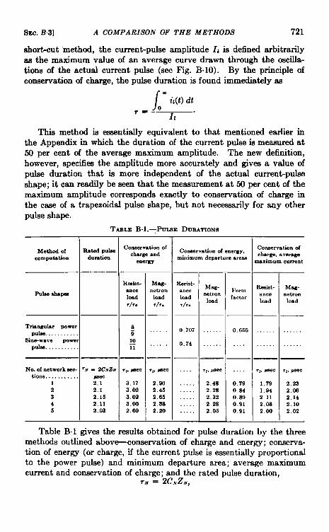
SEC. B.3] A COMPARISON OF THE METHODS 721
shorkut method, the current-pulse amplitude IL is defined arbitrarilyas the maximum value of an average curve drawn through the oscilla-tions of the actual current pulse (see Fig. B. 10). By the principle ofconservation of charge, the pulse duration is found immediately as
/
.i(t) dt
o7-=II “
This method is eaaentially equivalent to that mentioned earlier inthe Appendix in which the duration of the current pulse is meaaured at50 per cent of the average maximum amplitude. The new definition,however, specifies the amplitude more accurately and gives a value ofpulse duration that is more independent of the actual current-pulseshape; it can readily be seen that the measurement at 50 per cent of themaximum amplitude corresponds exactly to conservation of charge inthe case of a trapezoidal pulse shape, but not necessarily for any otherpulse shape.
TABLZ B.1.—PuIAE DUFtATIONS
Method cdcomputation
Triangular powerpulse . . . . . . . . .
Sine-wBve powepub . . . . . . . . . .
No. .afnetwork nec-tionn. .,,......
12345
Rmtuf W&Qduration
Tn - [email protected]
2.12.152.112.03
Conservation ofcharmmd
energy
Resist-anceload,/,.
Mag-netronload,/,.
—l——8
5 ‘“’”10ii ... ...
r,, Pbec
3.173.023.023.002.60
r,, *ec
2.902.452.652.3S2,20
Conservation of energy,minimum departure ai-em
Resist-ance1OW-I,/..
0.707
0.74
. . . . .
. . . . .
. . . . .
.
. . . .
I
Mw-Form
netronload
factor
I 0.656I
— —
‘-’cl ““2,4S2.282.322.282.05
0.790.s40.390.910.91
I
Conservation ofcharge, avere4e
maximum current
Resi8t-mceload
r,, Bsec
1 791.942.112.082cm
Mag-netronload
——
. .
r,, psec
2.23
2.06
2.142.102,02
Table B. 1 gives the results obtained for pulse duration by the threemethods outlined abov~onservation of charge and energy; conserva-tion of ener~ (or charge, if the current pulse is essentially proportionalto the power pulse) and minimum departure area; average maximumcurrent and conservation of charge; and the rated pulse duration,
TN = 2CNZN,
722 PULSE DURATION AND AMPLITUDE [SEC. B.3
of the pulse-forming networks. It maybe noted that, on magnetron load,the pulse durations determined by the last two methods do not diiTer bymore than 10 per cent, and that the pulse durations obtained by theshort-cut method are the nearest to the rated valuea of the networks.One great advantage of the short-cut method is its simplicity comparedwith either of the other two. Although it leads to values of pulse dura-tion that are slightly small, it does, on the other hand, give values forpulse currents that are too large in the same proportion. Since a smallincreaae in current may be more detrimental to the oscillator than asimilar increase in pulse duration, it is probably better, from a practicalstandpoint, to rate the pulser output on the basis of the third definition:less damage is likely to result to the magnetron from exceeding ratedcurrent, and, except for very nonrectangular pulses, the short-cut methodprovides a satisfactory definition of pulse amplitude and duration.

List of SymbolsIn the table that follows are listed the more important and extensively used sym-
bols appearing in this book. Many symbols used in particular developments havenot been included in the list when their usc is restricted ta relatively few pages ofthe text.
ENGLISHLETTER SYMBOE
Symbol Description De6ned or First Used
Aa
BAgBeB%B,B,,B-,
cc(!Dcdcmc,cNc.c,c.c.c●Nc.coc,
d
EbE*EcEcnE,,E,,
e:
%
PageCross-aectional area of PT core..... . . . . . . . . . . . . . . . . . . . . . . . . . . . . . . 510Thicbe~of layer of~whdmg . . . . . . . . . . . . . . . . . . . . . . . . . . . . . . . . . . 513
Average maguetic induction . . . . . . . . . . . . . . . . . . . . . . . . ... . . . . . . . . . . . . . 617Increment ofaverage flux density above remanent value of B. ..,,..... 537Flux density in charging reactor.. . . . . . . . . . . . . . . . . . . . . . . . . . . . . . . . . . 36sSome value of flux density lew than B~t . . . . . . . . . . . . . . . . . . . . . . . . . . . . 604Remanent flux density . . . . . . . . . . . . . . . . . . . . . . . . . . . . . . . . . . . . . . . . . . . 600Remanent tluxdensity in PT core with gap . . . . . . . . . . . . . . . . . . . . . . . . . 602Saturation flux density . . . . . . . . . . . . . . . . . . . . . . . . . . . . . . . . . . . . . . . . . . . . 600
Distributed capacitance of PT primary winding . . . . . . . . . . . . . . . . . . . 79,5o3Same as Cc for PT secondary winding . . . . . . . . . . . . . . . . . . . . . . . . . . . 79,508Capacitance ofdeapiking network . . . . . . . . . . . . . . . . . . . . . . . . . . . . . . 437Pbt~t~grid capacitance ofa vacuum tube . . . . . . . . . . . . . . . . . . . . . . . . . . 576Shunt capacitance dueto aloud.... . . . . . . . . . . . . . . . . . . . . . . . . . . . . . . . 79Energy storage capacitance ofa PFN. . . 127,176Capacitance between primary and secondary of PT . . . . . . . . . . . . . . . . . . . 507Capacitance ofrthaection ofa PFN. . . . . . . . . . . . . . . . . . . . . . . . . . . . . . . . 187Shunt capacitance, . . . . . . . . . . . . . . . . . . . . . . . . . . . . . . . . . . . . . . . . . . . 26hergystorage capacitance ktrigger generator . . . . . . . . . . . . . . . . .. J... 307Stray capacitance ofa PAN . . . . . . . . . . . . . . . . . . . . . . . . . . . . . . . . . . . . . . . 236Energy storage capacitance . . . . . . . . . . . . . . . . . . . . . . . . . . . . . . . . . . . . . 22Capacitance oflomlw transmiwion line.......................,..,.. 228Capacitance ofaectionuofa PFN (Guillemin theory ) . . . . . . . . . . . . . . . . . 192
Lamination thickness . . . . . . . . . . . . . . . . . . . . . . . . . . . . . 637
A-cpower supply voltage . . . . . . . . . . . 382D-cpower supply volt.age . . . . . . . . . . . . . . . . . . . . . . . . . . . . . .. .. ~....... 22Grid bias voltage . . . . . . . . . . . . . . . . 25Grid cuhffvoltage . . . . . . . . . . . . . . .576Control-grid voltnge (vacuum tulw. !JlScreen-grid voitage (vacuumtulw). . . . . . . . . . 91Applied grid voltage . . . . . . . . . . . . . . . . . .,,....,.....................576le, - E,~l. . . . . . . . . . . . . . . . . . . . . . . . . . . . . . . . . . . 576
723

724 LIST OF SYMBOLS
Symbol Description Defined or First Used
et
E
ff
tjojl
f2j:, f,GJgd
Q[
9P9.
HHeH=H.H,
I.,1,11InI=1P1,I,ZmbI=IS
I.
I.
I,
I.
L
i
iL
i;
A
~P
G
i,
io
iw
PageVoltage across load . . . . . . . . . . . . . . . . . . . . . . . . . . . . . . . . . . . . . . . . . . . ...563Electric field . . . . . . . . . . . . . . . . . . . . . . . . . . . . . . . . . . . . . . . . . . . . . . . . . . . . . 618
@jam . . . . . . . . . . . . . . . . . . . . . . . . . . . . . . . . . . . . . . . . . . . . . . . . . . . . . . ...6037/7mt. . . . . . . . . . . . . . . . . . . . . . . . . . . . . . . . . . . . . . . . . . . 535
Cut-off frequency forlow-pass filter... 184Pnlse recurrence frequency . . . . . . . . . . . . . . . . . . . . . . . . . . . . . . . . . . . . . . . 23Resonant frequency of charging circuit of a line-type puleer. . . . . . . . . 360Factor depending on voltage distribution between primary and secondary
of a PT . . . . . . . . . . . . . . . . . . . . . . ...522Factor relating LL to PT windingarrangement.. . . . . . . . . . . . . . . . . . 541Proportionalityfactore . . . . . . . . . . . . . . . . . . . . . . . . . . . . . . . . . . . . . . . . . . 541badconductance . . . . . . . . . . . . . . . . . . . . . . . . . . . . . . . . . . . . . . . . . . . . . . . . 208Shunt-diodeconductance. . . . . . . . . . . . . . . . . . . . . . . . . . . . . . . . . . . . 44Laad conductance. . . . . . . . . . . . . . . . . . . . . . . . . . . . . . . . . . . . . . . . . . . . . . . 28Switch-tubeconductance. . . . . . . . . . . . . . . . . . . . . . . . . . . . . . . . . . . . . 28Shunt conductance. . . . . . . . . . . . . . . . . . . . . . . . . . . . . . . . . . . . . . . . . . . . . . 34
Magnetizing force in PT . . . . . . . . . . . . . . . . . . . . . . . . . . . . . . . . . . . . . . . . . . 5J.3Coercive force . . . . . . . . . . . . . . . . . . . . . . . . . . . . . . . . . . . . . . . . . . . . . . . . . . . 601Magnetizing force in charging reactor. . 368Eddy-current magnetic field . . . . . . . . . . . . . . . . . . . . . . . . . . . . . . . . . . . . . 623Reverse magnetic field . . . . . . . . . . . . . . . . . . . . . . . . . . . . . . . . . . . . . . . . . . . . 601
Average current . . . . . . . . . . . . . . . . . . . . . . . . . . . . . . . . 3Puleecurrent in charging element . . . . . . . . . . . . . . . . . . . . . . . . . . . . 109Pulse current in load . . . . . . . . . . . . . . . . . . . . . . . . . . . . . . . . . . 22Magnetizing current.,.........,,.. . . . . . . . . . . . . . . . . . . 536Maximum current during apulse. . . . . . . . . . . . . . . . . . . . 51Current in PT primary . . . . . . . . . . . . . . . . . . . . . . . . . . . . . . . . . 71Plate current in switch tube..... . . . . . . . . . . . . . . . . . . . . . 22Current in PT primary . . . . . . . . . . . . 513
.Pulse current . . . . . . . . . . . . . . 3Effective current . . . . . . . . . . . . . . . . . 61Current in PT secondary . . . . . . . . . . . . . . . . . . . . . . . . . . . . . . . . . . . . . 71Current eourcereplacing voltage source V, . . . . . . . . . . . . . . . . . . . . . . . . . . 34Puleecurrent in shunt impedance . . . 109Current in PTeecondary . . . . . . . . . . 513Current source replacing charged storage condenser. ,. ..., . . . . . . 27Instantaneous current in charging element. . . . . . . . . . . . 60Eddy current . . . . . . . . . . . . . . . . . . . . .633Instantaneous current in inductance. . . . . . . . . . 23Instantaneous load curi-ent . . . . . . 23Magnetizing current . . . . . . . . . . . . . . . . . . . . . . . . . . . . . . . . . . . . . . . . . . 625Instantaneous plate current in switch tube . . . . . . . . . . . . . . . . . . . . . . . . . . 60Current inrthsection of PAN...... 180Instantaneous current in shunt path. . 40Initial current . . . . . . . . . . . . . . . . . . . . 62Current inmesh~of PFN(Guillemin theory).. . . . . . . . . . . . . . . . . . . . . . 192

LIST OF SYMBOLS 725
Symbol Description Defined or First Used
J
k
LLcL,II:DI.?I.LI..vIwI.,II:L“L;1..1/“s
Ilf
.NN..V,v1Pv,N,nn
~>*v
PL1’,l’mP,VP,I’RPFNPRFPTP
Q~NqN
PageDisplacem&t current . . . . . . . . . . . . . . . . . . . . . . . . . . . . . . . . . . . . . . . . . ...652
(coupling coefficien t . . . . . . . . . . . . . . . . . . . . . . . . . . . . . . . . . . . . . . . . . . 506
Average peripheral spacing of moving electrodes of rotary spark gap.. 284“Charging inductance” in series with distributed capacitance in PT 79, 508Inductance of isolating element . . . . . . . . . . . . . . . . . . . . . . . . . . . . . . . . . . . 62Charging inductance inline-typepulscr. . . . . . . . . . . . . . . . . . . . . . . . . . . . . 357&uncas Lcforthe other PT winding. . . . . . . . . . . . . . . . . . . . . . . . . . . . 79,508fMectives huntinductancei nP T.. . . . . . . . . . . . . . . . . . . . . . . . . . . . . 79,508Leakage inductance in PT . . . . . . . . . . . . . . . . . . . . . . . . . . . . . . . . . . . . . 79,512Inductance ofa PAN . . . . . . . . . . . . . . . . . . . . . . . . . . . . . . . . . . . . . . . . . . . . 127Primary inductance of PT . . . . . . . . . . . . . . . . . . . . . . . . . . . . . . . . . . . . . . . . 510Inductance ofrthsection of PAN . . . . . . . . . . . . . . . . . . . . . . . . . . . . . . . . . . . 187Value ofinductance forresonant charghg. . . . . . . . . . . . . . . . . . . . . . . . . . . 360Shunt Inductance . . . . . . . . . . . . . . . . . . . . . . . . . . . . . . . . . . . . . . . . . . . . . . . . 39Energy storage inductance . . . . . . . . . . . . . . . . . . . . . . . . . . . . . . . . . . . . . . . 22Total distributed inductance of lossless transmission line . . . . . . . . . . . . . . 209Inductance of section u of PFN (Guiflemintheory) . . . . . . . . . . . . . . . . . . 192Mcanmagnetic path length. . . . . . . . . . . . . . . . . . . . . . . . . . . . . . . . . . . . . . . 510Lengthofgapin PT core. . . . . . . . . . . . . . . . . . . . . . . . . . . . . . . . . . . . . . . . . 602Lengthof PT winding. . . . . . . . . . . . . . . . . . . . . . . . . . . . . . . . . . . . . . . . . . . 513
Mutual inductance. . . . . . . . . . . . . . . . . . . . . . . . . . . . . . . . . . . . . . . . . . . . . . . 505
Numbcrof turnsof PT coil. . . . . . . . . . . . . . . . . . . . . . . . . . . . . . . . . . . . . . . 51ONumherof turnson chargingreactor.. . . . . . . . . . . . . . . . . . . . . . . . . . . . . . 364Numberof fixcdelectrodesofmtary gap. . . . . . . . . . . . . . . . . . . . . . . . . . . . 282iNumberofturns on PT primary. . . . . . . . . . . . . . . . . . . . . . . . . . . . . . . . . . . 513Numherof moving electrodesof rotarygap. . . . . . . . . . . . . . . . . . . . . . . . . 282Numbcrof turnson PT secondary.. . . . . . . . . . . . . . . . . . . . . . . . . . . . . . . . 513Voltage transformationratio of a transformer... . . . . . . . . . . . . . . . . . . . . . 71Numberofmeshes ina PAN. . . . . . . . . . . . . . . . . . . . . . . . . . . . . . . . . . . . . . MO
Avemgepower. . . . . . . . . . . . . . . . . . . . . . . . . . . . . . . . . . . . . . . . . . . . . . . . . . . 3Overheadpower loss inline-type pul=r... . . . . . . . . . . . . . . . . . . . . . . . . . . 249R&cpowerinaloud . . . . . . . . . . . . . . . . . . . . . . . . . . . . . . . . . . . . . . . . . . . . . 70Maximumpowerduringa pulse.... . . . . . . . . . . . . . . . . . . . . . . . . . . . . . . . . 714Powerinput to PFN . . . . . . . . . . . . . . . . . . . . . . . . . . . . . . . . . . . . . . . . . . . . . 392Pulsepowerdissipatedin switch tube. . . . . . . . . . . . . . . . . . . . . . . . . . . . . . . 72Powerdissipatedinkolatingresktance. . . . . . . . . . . . . . . . . . . . . . . . . . . . . 61Pulseformingnetwork. . . . . . . . . . . . . . . . . . . . . . . . . . . . . . . . . . . . . . . . . . . . 8Pulserecurrencefrequency. . . . . . . . . . . . . . . . . . . . . . . . . . . . . . . . . . . . . . . . ‘JPulsetransformer. . . . . . . . . . . . . . . . . . . . . . . . . . . . . . . . . . . . . . . . . . . . . . . .Laplacetransformparameter. . . . . . . . . . . . . . . . . . . . . . . . . . . . . . . . . . . . . . 28
Quality factor of a circuit.. . . . . . . . . . . . . . . . . . . . . . . . . . . . . . . . . . . 12, 360Chargeona PF51. . . . . . . . . . . . . . . . . . . . . . . . . . . . . . . . . . . . . . . . . . . . . . . . 176Instantaneouschmgeona PFN. . . . . . . . . . . . . . . . . . . . . . . . . . . . . . . . . . . . 356

726 LIST OF SYMBOLS
Symbol Description Defined or First Used
R.RdR,ROR.RIR,R,R,RwR@
Torl
rPr,
s,SISuST
T
T
TbT,t,
‘-u
v,.(t)Vc(t)V@v,vJ,VIVI”vMv-
Vmi.
VA.vNmVN-.Vpv,v(p)Vs
PageResistance of isolating element in charging circuit of a pulser. . . . . . 26, 357Resistance ofdespiking network . . . . . . . . . . . . . . . . . . . . . . . . . . . . . . . . . . 437Shunt resistance in PT . . . . . . . . . . . . . . . . . . . . . . . . . . . . . . . . . . . . ...236.508Internal resistance ofvoltageeource. . . . . . . . . . . . . . . . . . . . . . . . . . . . . . . . 501Ieolating resistance in grid circuit of a vacuum tube. . . . . . . . . . . . . . . . . . 25Load resistance . . . . . . . . . . . . . . . . . . . . . . . . . . . . . . . . . . . . . . . . . . . . . . . . . . 22Switch resistance plus series losses in PFN and PT . . . . . . . . . . . . . . . . . . . 236Resistance inparallel with pulaer output . . . . . . . . . . . . . . . . . . . . . . . . . . . . 33T,/w . . . . . . . . . . . . . . . . . . . . . . . . . . . . . . . . . . . . . . . . . . . . . . . . . . . . . . . . . . . . 637Resistance of PT winding . . . . . . . . . . . . . . . . . . . . . . . . . . . . . . . . . . . . . . . 506wpld . . . . . . . . . . . . . . . . . . . . . . . . . . . . . . . . . . . . . . . . . . . . . . . . . . . . . . . . . . . 637Grid-to-cathode resistance of vacuum tube . . . . . . . . . . . . . . . . . . . . . . . . . . 575Dynamic resistance of a load (magnetron or biased diode).. . . . . . . . . . . . 33Internal resistance of switch tube... . . . . . . . . . . . . . . . . . . . . . . . . . . . . . . . 22Resistance between two laminations of PT core . . . . . . . . . . . . . . . . . . . . . . 637
Hypothetical switch in series with shunt diode. . . . . . . . . . . . . . . . . . . . . . . 44Hypothetical switch inseriea with diode load . . . . . . . . . . . . . . . . . . . . . . . 33Hypothetical switch iuaeri~ with magnetron. . . . . . . . . . . . . . . . . . . . . . . . 46Switch tube . . . . . . . . . . . . . . . . . . . . . . . . . . . . . . . . . . . . . . . . . . . . . . . . . . . . . 27
Symbol fora tube . . . . . . . . . . . . . . . . . . . . . . . . . . . . . . . . . . . . . . . . . . . . . . . . 74p,a,$ lo-%@~ usingmks unite or —
3pusing c~ unita . . . . . . . . . . . . . . . . . . ...623
Deionizing time . . . . . . . . . . . . . . . . . . . . . . . . . . . . . . . . . . . . . . . . . . . . . . . . . 487Pulse recurrence interval (l/f,) . . . . . . . . . . . . . . . . . . . . . . . . . . . . . . . . . . . . 3Riitime ofapulee . . . . . . . . . . . . . . . . . . . . . . . . . . . . . . . . . . . . . . . . . . . . . .537
Average circumference of layer of PTwinding . . . . . . . . . . . . . . . . . . . . . . . 513
Voltage acrosaoutput of hard-tube puhwr. . . . . . . . . . . . . . . . . . . . . . . . . . . 27Time function of voltage across a capacitance. . . . . . . . . . . . . . . . . . . . . . . . 53Source or generator voltage . . . . . . . . . . . . . . . . . . . . . . . . . . . . . . . . . . . . . . . . 532Pulee grid voltage . . . . . . . . . . . . . . . . . . . . . . . . . . . . . . . . . . . . . . . . . . . . . . . . 25PFN voltage at end of a pulse due to impedance mismatch = VN-,. 419Pulse voltage across a loud . . . . . . . . . . . . . . . . . . . . . . . . . . . . . . . . . . . . . . . . 22Voltage ofnthreflected pulse at the load . . . . . . . . . . . . . . . . . . . . . . . . . . . 418Observed value of V_ . . . . . . . . . . . . . . . . . . . . . . . . . . . . . . . . . . . . . . . . . . 297Maximum voltage across a series gap switch for which preflring is negligi-ble . . . . . . . . . . . . . . . . . . . . . . . . . . . . . . . . . . . . . . . . . . . . . . . . . . . . . . . . . . . . . 297Mtilmum voltage across a series gap switch for which misfiriig is negligi-ble . . . . . . . . . . . . . . . . . . . . . . . . . . . . . . . . . . . . . . . . . . . . . . . . . . . . . . . . . . . . . 298Initial voltage ona PAN . . . . . . . . . . . . . . . . . . . . . . . . . . . . . . . . . . . . . . . . . . 176PFNvoltage atendof nthchargkg period . . . . . . . . . . . . . . . . . . . . . . . . . . 419PFNvoltage atendof nth reflection. . . . . . . . . . . . . . . . . . . . . . . . . . . . . . . . 418PT primary voltage . . . . . . . . . . . . . . . . . . . . . . . . . . . . . . . . . . . . . . . . . . . . . . 71Voltage drop across switch tube . . . . . . . . . . . . . . . . . . . . . . . . . . . . . . . . . . . . 22Laplace transform of V(t) . . . . . . . . . . . . . . . . . . . . . . . . . . . . . . . . . . . . . . . . . 28PT secondary voltage . . . . . . . . . . . . . . . . . . . . . . . . . . . . . . . . . . . . . . . . . . . . 71

LIST OF SYMBOLS 727
Symbol Description De6ned or First Used
Vsv,
v-v.v.v:v.VTv;VI%
www.WIw.WNw
YY?f
Z1Z.Vz,z,ZTZ(!
a
a
d
P
Y
Yr,rL
AAP
66
PageTheoretical maximum value of V_. . . . . . . . . . . . . . . . . . . . . . . . . . . . . . . . 297Voltage at which conduction starts in an ideal diode; starting voltage of amagnetron . . . . . . . . . . . . . . . . . . . . . . . . . . . . . . . . . . . . . . . . . . . . . . . . . . . . . . 32Minimum power supply voltage at which 6ring occurs for seriesgaps. . . 298Voltage source equivalent to charged energy storage condenser. 27Equihbrium value of storage condenser voltage, . . . . . . . . . . . . . . . . . . 53Energy storage condenser voltage at the start of a particular pulse.. . . . 53Initial voltage onloedees transmieeion line . . . . . . . . . . . . . . . . . . . . . . . . . . 177Equilibrium value of storage condenser voltage at the end of a pulse, 53Energy storage condenwr voltage at the end of a particular pulse. . . . . . 53Instmtan~us voltage acre= a load . . . . . . . . . . . . . . . . . . . . . . . . . . . . . . . . 237Instantaneous-voltage drop across switch tube. . . . . . . . . .‘. . . . . . . . . . . 60
Energy in magnetic field . . . . . . . . . . . . . . . . ... . . . . . . . . . . . . . . . . . . . . . . . . 513Energy ina charged capacitance. . . . . . . . . . . . . . . . . . . . . . . . . . . . . . . . . . . 519Energy dissipated in PT core due to eddy currents . . . . . . . . . . . . . 627Energy dissipated in a loud . . . . . . . . . . . . . . . . . . . . . . . . . . . . . . . . . . . . . . . 226Energy returned tothecircuitfrom PT core . . . . . . . . . . . . . . . . . . . . . . . . . 628WergystoA in PFN . . . . . . . . . . . . . . . . . . . . . . . . . . . . . . . . . . . . . . . . . . . . 25oWidth of core lamination . . . . . . . . . . . . . . . . . . . . . . . . . . . . . . . . . . . . . . . . . . 637
Admittance = l/Z . . . . . . . . . . . . . . . . . . . . . . . . . . . . . . . . . . . . . . . . . . . . . . . 185Admittance ofa PFN . . . . . . . . . . . . . . . . . . . . . . . . . . . . . . . . . . . . . . . . . . . . 208
Load impedance . . . . . . . . . . . . . . . . . . . . . . . . . . . . . . . . . . . . . . . . . . . . . . . . . 84Impedance ofa PAN . . . . . . . . . . . . . . . . . . . . . . . . . . . . . . . . . . . . . . . . . 129,176Internal impedance ofapulser . . . . . . . . . . . . . . . . . . . . . . . . . . . . . . . . . . . . . 85Impedance inparallel with pulser load. . . . . . . . . . . . . . . . . . . . . . . . . . . . . . 33Characteristic impedance of PT winding. . . . . . . . . . . . . . . . . . . . . . . . . . . . 523Characteristic impedance of a transmission line. . . . . . . . . . . . . . . . . . 84
GREEK LETTER SYMBOIS
Sbntl~coe5cient =l+z~ . . . . . . . . . . . . . . . . . . . . . . . . . . . . . . 238.
PT parameter . . . . . . . . . . . . . . . . . . . . . . . . . . . . . . . . . . . . . . . . . . . . . . . . 533
Series lose coefficient =l+z% . . . . . . . . . . . . . . . . . . . . . . . . . . . . . . . . . ...238
PT parameter . . . . . . . . . . . . . . . . . . . . . . . . . . . . . . . . . . . . . . . . . . . . . . . . 533
Ratio of total load distributed capacitance to PFN capacitance . . . 252.
~-%, . . . . . . . . . . . . . . . . . . . . . . . . . . . . . . . . . . . . . . . . . . . . . . . . . . . . . . . . . 419
I/L= . . . . . . . . . . . . . . . . . . . . . . . . . . . . . . . . . . . . . . . . . . . . . . . . . . . . . . . . . . . . 591loll . . . . . . . . . . . . . . . . . . . . . . . . . . . . . . . . . . . . . . . . . . . . . . . . . . . . . . . . . ...591
Distance between layers of PT winding. . . . . . . . . . . . . . . . . . . . . . . . . . . . . 513Skhdepth . . . . . . . . . . . . . . . . . . . . . . . . . . . . . . . . . . . . . . . . . . . . . . . . . . . . . . 548
One way transmission time for loseless tmnsmission line. . . . . . . . . . 177, 524Loeetangent =tani$ . . . . . . . . . . . . . . . . . . . . . . . . . . . . . . . . . . . . . . . . . . . . 653

728 LIST OF SYMBOLS
Symbol Description Defined or Fmt UcedPage
Dielectric constant . . . . . . . . . . . . . . . . . . . . . . . . . . . . . . . . . . . . . . . . . . . . . . . 519Small positive voltage . . . . . . . . . . . . . . . . . . . . . . . . . . . . . . . . . . . . . . . . . . . 576Dielectric constant of free space . . . . . . . . . . . . . . . . . . . . . . . . . . . . . . . . . . . . 618Dielectric constant of core material in mks units . . . . . . . . . . . . . . . . . . . . 618
Efficiency of a PT..., . . . . . . . . . . . . . . . . . . . . . . . . . . . . . . . . . . . . . . . . . . . . 71Efficiency of power supply . . . . . . . . . . . . . . . . . . . . . . . . . . . . . . . . . . . . . 249Efficiency ofcharging circuit . . . . . . . . . . . . . . . . . . . . . . . . . . . . . . . . . . 249Efficiency ofdiwharging circuit . . . . . . . . . . . . . . . . . . . . . . . . . . . . . . . . . . . . 249Efficiency ofpulser circuit, . . . . . . . . . . . . . . . . . . . . . . . . . . . . . . . . . . . . . . . .249Efficiency of a PT . . . . . . . . . . . . . . . . . . . . . . . . . . . . . . . . . . . . . . . . . . . . ...236berallefficiency ofapuleer . . . . . . . . . . . . . . . . . . . . . . . . . . . . . . . . . . . . . . . 249
Reflection coefficient . . . . . . . . . . . . . . . . . . . . . . . . . . . . . . . . . . . . . . . . . . 85,419
Amphfication factor . . . . . . . . . . . . . . . . . . . . . . . . . . . . . . . . . . . . . . . . . . . 91,576Permeability . . . . . . . . . . . . . . . . . . . . . . . . . . . . . . . . . . . . . . . . . . . . . . . . . . . . 523Effective puleeperrneability . . . . . . . . . . . . . . . . . . . . . . . . . . . . . . . . . . . . . . 51oD-c incremental permeability . . . . . . . . . . . . . . . . . . . . . . . . . . . . . . . . . . . . . . 601D-c incremental permeability for core with gap. . . . . . . . . . . . . . . . . . . . . 601Maximum permeability . . . . . . . . . . . . . . . . . . . . . . . . . . . . . . . . . . . . . . . . . . . 603Average permeability . . . . . . . . . . . . . . . . . . . . . . . . . . . . . . . . . . . . . . . . . . . . . 601Average permeability for core with gap . . . . . . . . . . . . . . . . . . . . . . . . . 601Permeability inmks units . . . . . . . . . . . . . . . . . . . . . . . . . . . . . . . . . . . . . 618
Reeietivity . . . . . . . . . . . . . . . . . . . . . . . . . . . . . . . . . . . . . . . . . . . . . . . . . . . . . . 511
PT circuit parameter . . . . . . . . . . . . . . . . . . . . . . . . . . . . . . . . . . . . . . . . . 564Conductivity ofcorematerial inmke units. . . . . . . . . . . . . . . . . . . . . . . . . . 618
Pulse duration . . . . . . . . . . . . . . . . . . . . . . . . . . . . . . . . . . . . . . . . . . . . . . . . . . 3Duration of power pulse . . . . . . . . . . . . . . . . . . . . . . . . . . . . . . . . . . . . . . . . . 714Pulwduration at theload, . . . . . . . . . . . . . . . . . . . . . . . . . . . . . . . . . . . . . . . . 250Maximum pulee duration obtainable with a regenerative pulse generator 587Pulse duration produced by a PFN on a matched resistance load . . . 250‘l%nerequire dtosaturat eacorelamination. . . . . . . . . . . . . . . . . . . . . . . . . 634
Circuit parameter . . . . . . . . . . . . . . . . . . . . . . . . . . . . . . . . . . . . . . . . . . . . . . 42Angular frequency ofa-c voltage . . . . . . . . . . . . . . . . . . . . . . . . . . . . . . . . . . . 177~s=w; —a%. . . . . . . . . . . . . . . . . . . . . . .,, ,, . .,, ,,, ,, ... ,, ...,,,,,.,,357Applied a-c angular frequency . . . . . . . . . . . . . . . . . . . . . . . . . . . . . . . . . . . . . 367
1~;=— LCCN. . . . . . . . . . . . . . . . . . . . . . . . . . 357

Index
A
A-c charging dicde, 414-416general analysis of, 380-386nonresonant, 381, 365, 393-400remnant, 381, 365, 386393
average-current component in, 369charging-circuit efficiency in, 392circuit utilization factor in, 392
A-c charging transformers, linearityrequirements for, 401
practical, 400-407A-c impedance, 177Airborne radar systems, light-weight
medium power pulaer for, 140-152Aluminum-cathode gap (see Fixed gap)Amplitude jitter, 290, 331Anger circuit, 466-471Anode buildup, 320Anode circuit, 344-349
of hydrogen thyratrons, 344Anode current, rate of rise of, 348Anode voltage, forward, 346
inverse, 346-348Arnott, E. G. F., 321n., 324n.Autotransformer, 512Average current, 361, 467, 470, 483Average=current component in a-c reso-
nfit charging, ~9Average-current measurements, 146Average-current meter, 701–706Average values of the transformer
rents, 396
B
Backswing voltage, 43, 45, 50, 79, 88,146, 154, 261, 509, 551, 569
Bell Telephone Laboratories, 104, 281,295, 317, 321, 322, 328, 472-476
Bettler, P. C., 451n.B-H 10cIP,d-c, 612
idealized, 633idealized and actual pulse, 627pllke, 612, 643
circuit for, 641B-H oacillograms, for a-c charging trans-
formers, 403, 405, 406for d-c charging reactm, 369, 370
Bias, cutoff, for tetrode, 100for triode, lCMI
negative, 92Bias voltage, cutoff, 99Biased diode, curmmt.-vokage character-
iatic of, 32, 231Biased-diode load, 527Blocking-oscillator driver, 124–132Blocking-oscillator transformer, design
of, 543-547Blumlein circuit, 465-468Bootstrap driver, 120-124, 138Bostick, W. H., 611n.., 639n.Breakdown field of rotary gap, 291Breakdown time of rotary gap, 275Breakdown voltage, dynamic, of single
fixed gap, 296static, of single fixed gap, 296
Bushings for pulse transformers, 654Butt joint in core, 601, 644Byerly, W. E., 656n.
c
Cable, matched, with a series resistor, 671with a shunt resistor, 671
for pulse-forming network, 164Cable impedance matching, 671Cable-matching, 677Cable properties and delay lines, 689Capacitance divider, 673-675
729

730 PULSE GENERA TORS
Carslaw, H. S., 27n.Cathode and anode erosion of fixed gap,
319-321Cathode current, 148Cathode erosion, 317, 320Cathode follower, 121, 125Cathode fatigue, 97Cauer’s extension of Foster’s theorem,
194Chaffee, E. L., 98n.Characteristic current-voltage of a non-
linear load, 110Characteristic curves for triodes and
tetrodes, 98-108Characteristic impedance (see Imped-
ance, characteristic)Characteristics, grid-current–plate-volt-
age, 101–108idealized current-voltage, of a tetrode,
110plate-current-grid-voltage, 99-101plate-current–plate voltage, 101–108
Charging, of storage condenser, 5149(See also A-c charging; D-c charging;
Full-cycle charging; Half-cyclecharging; Inductance charging;Linear charging; Recharging; Res-onant charging
Charging-circuit eficiency in a-c resonantcharging, 392
Charging-circuit 10SZCS,429Charging circuits, of lime-type prdser,
355-416miscellaneous, 414416
Charging cycle, 358Charging diode, 138, 361
(See also Hold-off diode)Charging efficiency, 392, 421Charging element, inductance, 355
resistance, 355Charging inductance, 361, 455, 467,
483of a pulse transformer, 523-530
Charging period, 384Charging reactor, 356
coil design for, 372core design for, 372linearity of, 366sample design for, 376saturation of core, 364, 370
Charging transformer losses, 413
Charging transformers, a-c, (see A-c
charging transformers)Charging voltage, forward, measurement
of, 69W592Circuit (see type of circuit)Circuit complexity, 16Circuit utilization factor in a-c r~n~t
charging, 392Coding, pulse-, 131, 486Coil design for d-c charging reactor, 372Gil material for pulse transformers, 648-
660Cole, P. A., 662n., 706n.Condenser, as energy reservoir, 21–23
discharging of, 25-51storage, charging of, 51-69
effect of inductance of isolating ele-ment on, 67
voltage on, 77Ccmdeneer voltage equilibrium, 53, 55Connectors, for pulse transformers, 654Conservation of charge, definition of
equivalent rectangular pulse, 711-716
Conservation of energy, definition ofequivalent rectangular pulse, 711-716
Core, accurate equivalent circuit for, 631with butt joints, 601, 644without butt joints, 600magnetization of, 633
Core design for d-c charging reactor, 372Core material for pulse transformers,
599-648d-c data for, 614-015d-c properties of, 599-%01pulse data for, 614-615standard teats on, 611thickness of, 599
Core performance, techniques for measur-ing, 639-648
Core maturation, 603n.Core size, 538, 545Coupling c0e5cient, 506Craggs, J. D., 274n.,332Crout, P. D., 528Current, average (see Average current)
effective (see EMective current)Current-fed network (see Network)Current modes in pulse transformer,
528

INDEX 731
Current pulse, 175, 176, 666amplitude for, 69
Current pulse droop, 80,88, 169, 568,702(See aZso pulse droop)
Current pulse rectangular in copper, 655-658
Current-pulse shapes, 186Current-pulse-viewing resistors, 676Current spike (see Spike, current)Current-viewing resistors, 666Current-voltage characteristics of a bi-
ased diode, 32, 231CV85 trigatron, 332CV125 trigatron, 332
D
Darlington circuit, 464D-c charging, 356-380
general analysis of, 356-363D-c charging current from nordinear
charging reactor, 365D-c charging reactors, design of, 372–380
linearity requirements for, 364-366practical, 364-372
D-c charging voltage from nonlinearcharging reactor, 365
D-c hysteresis loop, 605of a core, 600
(See d-so B-H kmp)D-c incremental permeability, 601, 632,
634D-c permeability, 510D-c resonant charging, 360,418Deionisation, 279Deionisation time, 336, 353Delay line, 133, 158Delay lines and cable properties, 689Delay time, 351Despiking circuit, 453Despiking RC-network, 436Diaplex, 215Dielectric, dissipation factor of, 216Dielectric constant and power factor, 652Dielectric strength, 651Dielectrics, 215Diffusion equations, 656
development of, 617-619edution of, 619-626
Dillinger, J. R., 312n., 320n., 324n., 327n.,335n.
Diode, biased (s= Biaaed diode)Discharging of storage condenser, 25-51Discharging circuit, effect of, on pulse
shape, 255-261efficiency of, 449general properties of, 225-233of line-type pulwr, 225-272
Discharging efficiency, 466, 4S3Discharging (pulse) interval, 54Dissipation factor of dielectric, 216Distributed capacitance, 516-522, 537
effective, of pulse-tr~*fOrmer coi~,measurement of, 521
for a transformer, 507Divider (see specific type of divider)Donovan, A C., 367n.Double-switch single-network circuit,
4S8-492Drewell, P., 336n.Driver, 119
blocking+scillatir, 124–132bootstrap, 120-124, 13Smultivibrator, 132–139puIs&forming-network, 132–139regenerative, 124-134, 150
Driver circuits, 119-139, 157, 168Dry type of insulation, 64=51
eolventleac varnish for, 649Dunham, C. R., 619n., 635n.Duolaterally wound coil, 554Dupont, 650Duration (see Pulse duration)Duty, 4Duty cycle, 4Duty ratio, 4Dynamic resistance, 231
of load, 3, 33, 78, 110
E
Eddy current, 620, 624, 636energy dissipated by, 626
Eddy current loss, 629Effective current, 361
in a-c resonant charging circuit, 390in transformer windina 547
Effective current density, in transformerwinding, 548
Effective values of the transformer cur-rents, 396

732 PULSE GENERATORS
Efficiency, 13, 534of hard-type pulser, 16of line-type puleer, 13, 16pulser, 244, 249-255, 462
of line-type pulser, 249over-all, 249of rectifier circuit, 249total, 249
829tetrode, 105, 123, 126,132SS4 tube, 1238020 shunt diode, 154Electrode material, for fixed gap, choice
of, 317for rotary gaps, 280
Electrodes, 6xed, 276moving, 276for rotary gaps, number of, 282
Energy, dissipated, in the core, calcula-tion, 627
approximate, 630by eddy currents, 626in puke-trmefor’mer windings, 660
stored in magnetic field, 627Energy density, average, in coil, 541
in core, 541Energy loss, 62t%633Ehergy reservoir, comparison of a con-
denser and an inductance aa, 23-25(S.. also Condenser; Inductance)
Energy transfer, maximum, 533Equivalent circuit, for pule.c+transformer
core, 626-633(See m!eocomponent for which equiv-
alent circuit is given)Erosion of electrodes of ilxed gap, 319-
321Evans Signal Laboratory, 342ra.
F
Fe-I gap, 3285C22 thyratmn, 138, 341, 4555D21 tetmde, 100, 104, 132,472527 triode, 106Fixed gap, aluminum-cathode, 298
designs of, 321–323cathode rmd anode erosion of, 319-321cylindrical electrode, 295cylindrical-electrode aluminum-cath-
ode, 318-327enclosed, 29&335
Fixed gap, iron-sponge mercury-cathode,327–332
designs of, 328mercury-cathode, 295, 303
(See af.90Series gap)static- and dynamic-breakdown volt,-
ages of a single, 296three-electrode, 332–335
hydrogen-fifled, 335types (see listing under O)
Fixed gap design, general considerationsfor, 31t%318
Fixed gap dissipation, 324–326, 331Fixed spark gap (see Fixed gap)Fletcher, R. C., 680n.Fluharty, R. G., 274n., 326n.Flux density, 538
distribution of, 623incremental, 537
Fluxplot, for typical puke-transformingwinding, 659
Fosterite, 557,649, 650Foster’s reactance theorem, 193Foster’s theorem, Cauer’s extension of,
1944C35 thyratron, 138, 341, 479Fourier-eeries, 187Frank, R., 656n.Frequency response, of pulse transformer,
591-598of transformer, oscilloscope presenta-
tion of, 595Full-cycle charging, 39+397, 449Fundingsland, O. T., 443n.
G
Ganz, A. G., 623n., 628n., 633n.Gap in the core, 601
(See ako Fixed gap; Rotary gap;Series gap)
Gap length of the core, optimum, 602-604Gap restriking, 279Gap spacing, 32oGaps, number of, vs. voltage range, 300-
302Gardner, M. F., 27n.Gas, for tixed gap, choice of, 316
for rotary gaps, 280Gas cleanup, 336Gas pressure, 3X3Gaseous-discharge switch, 10, 14, 175

INDEX 733
GE 68G627 pulse transformer, 129, 150General Electric Company, 355n., 373,
400402,408, 557,559,614415,638,649
Geometry of fixed gap, determination of,318
Germezhausen, K. J., 312n., 335n.Gibbs phenomenon, 187Gillette, P. R., 522n.Glasoe, G. N., 662n., 707n.Glick, H. L., 327n.Coucher, F- S., 274n., 295n., 316n., 318n.,
327n., 331n.Grid, power dissipation in, 97Grid circuit of hydrogen thyratron, 349-
354Grid current, 97Grid drive, positive, 91Grid-driving power, 157Grid swing, 92, 119Guillemin, E. A., 189n., 193n.Guillemin networks, 200-203
current-fed, 211–213type A, 212type B, 212type c, 212type F, 212
voltage-fed, type A, 201type B, 201type C, 201type D, 201type E, 201
Guillemin’s theory, 189-207
H
Half-cycle charging, 397400Half-wave single-phase charging, 476478Hanna, C. R., 377n.Hard-tube pulser, 5, 68, 19-172
application of pulse-shaping networksto, 165-172
comparison of, with line-type pulzer,13-17
high-power short-pulse, 160-165lightweight medium power, 140-152lMw, 152–160output circuit of, 21–89required switch characteristics of, 90-
98two arrangements of uw of pulse
transformer with, 74
Haynes, J. R., 295n., 303n.Heat dissipation, 151, 459Hibbard, L. U., 693n.High-reactance transformers, design of,
407414Hipersil pulse-transformer cores, 610Hold-off diode, 163, 381, 414416, 456
(See ako Charging diode)Hull, A. W., 274n.Hydrogen thyratron, 335-354
anode circuit of, 344control-grid characteristic in, 338grid circuit of, 349-354life of, 341operating characteristics of, 336-344operation of, 339
series and parallel, 842tube characteristics of, 339
Hysteresis loop on an oscilloscope, 639-641
(See also B-H loop)Hysteresis loss, 627
I
ZTVP curve, 111-118Ionization, residual, 297Ionization time, 345Impedance, a-c, 177
characteristic, 176of pulse-forming network, 9, 129
instantanemrs, 437internal, of pulzer, 4mismatch, 417of a network, measurement of, 221
Impedance characteristic, of a cable, 670of a pulse transformer, 522–526
Impedance-matching, 4, 9, 13, 16, 227cable, 671, 677to load, 70-76and transmission cable, 66M73
Impedance mismatch with long cable,reflection effects of, 84-89
Impedance transformation ratio, of trans.former, 10
Inductance, as the energy reservoir, 23Inductance charging, from an a-c source,
380-386(See ako A-c charging)
from d-c power supply, 356-380efficiency of, 363
Inductance measurements, 366-372

1
734 PULSE GENERATORS
Inductive kicker, 305-307Ingram, S. B., 295n.Input capacitance of load, 536Insulating materials, measurements on,
653Insulation for pulse transformers, 648-655Interlaminar insulation, 638Interlaminar resistance, 636-638Intarpulw interval 16,54, 119Iron-sponge mercury-cathode gap (see
Fixed gap)Iecdating element, 6, 12, 52
average power dissipated in, 59effect of inductance of, on charging of
storage condencer, 67high resistance as, 52-61inductance, 61-69, 145inductive resistor as, 61+9principal advantages of inductance ea,
68resistance, 153
J
Jitter, time (we Time jitter)Joos, G., 501n.
K
Keyers, 1Kicker, inductive, 305-307Kraft paper, 551Krulikoeki, S. J., 344n.J 347n.
1
Laplace-transform method, 27, 175Leading edge of puke (see Pulee)Leakage core, 400
separate, 409Leakage inductance, 506, 511-516
calculation of, 512measurement of, 515of traneforme~, 400
Leakag+reactanc=ore gap, 411Lebacqz, J. V., 274n., 468n.Linear charging, 12, 361Linearity requirements for a-c charging
transformers, 401Lin-imulating network, 124, 180
(S= &o Network)
Line-type pulse generator with a magnetron load, 573
Line-type pulaer, 5, 8-12, 173-496characteristics of, 233-244charging circuit of, 355-416
measurement in, 690comparison of, with hard-tube pulser,
13-17discharging circuit of, 225-272efficiency of, 13, 16, 249equivalent circuit, 236-238performance of, 417-447switches for, 234, 273-354
Line-type puleer characteristics, 233-244Lirwvoltage variation, 117Load, coupling to, 70-76
directiconnected, 73duration of pulse at, 226dynamic resistance of, 3, 33, 78, 110energy dissipated in, 226linear, 3nonlinear, 3open circuit in (see Open circuit)puke power in, 226resistance, 177short circuit in (see Short circuit)static resistance of, 3, 110transformer-coupled, 73
Load characteristics, effect of on puleerregulation, 108-118
Lead current, change in, during a pulse,58
reducing the change in, 166Load current variation, 117Load dynamic resistance, 78Load effect on pufaer operation, 418-423Load impedance, effects of change in,
417Load line, 238-244Load voltage, 469Lees, series, 237, 238
shunt, 238
M
Mac(ldl, L. A., 61%.MacFayden, K. A., 63%.McIntosh, R. O., 693n.Magnetic-path length, mean, 509Magnetio shunt, 4CKIMagnetizing current, 522

INDEX 735
Magnetron, current voltage character.ietic of, 32, 702
mod-changing of, 206, 417, 438-441mode-skipping, 439normal operation of, 435438pushing figure of, 118sparking of, 425, 441447, 707
Magnetron current, average, 146, 155,253
Magnetron-input characteristics, 435Magnetron load, 527
puleer performance with, 435447, 707Marx circuit, 494Maxwell’s equations, 618Measurement (see quantity measured)Meaauring techniques, 661–709Mechanicaldesign considerations for ro-
tary gaps, 283-289Megaw, E. C. S., 693n.Metering techniques in pulse meaeur~
ments, 692-709Mica, 215Minimum departure areas, equivalent
rectangular pulse by, 716-720Mode changing of magnetrons, 206, 417,
438441Mode skipping, 438Mode-skipping magnetron, V-I charac-
teristics of, 439Modulators, 1Moody, F. N., 500n.Motor, 285Multipk+switch circuit for voltage mul-
tiplication, 494496Multiple-switch multiple-network cir-
cuit, 485488Multivibrator, biaaed, 132Multivibrat.or driver, 132-139
N
Naval Research Laboratory, Anacostia,D. C., 171
Network, average power supplied by, 253currenGfed, 8, 25, 135, 175, 207–213of equal capacitance per section, 196-
200, 203-207Guillemin, 200-203, 211-213initial charge on, 176inverse voltage on, 427line-simulating, 124, 180
Network, mutual inductance, 199puleeforming, 8, 175,224,225,234,356
cable se, 164characteristic impedance of, 9, 129current-fed, 25voltage on, 454
type A, 201, 212type B, 201, 212type C, 201, 2!2type D, 201, 205type E, 205, 213, 219type F, 201, 212voltage-fed, 8, 175, 189-207
Network attenuation, 222Network capacitance, 454Network-charging circuit, 12Network coils, 213-215
construction of, 221Network condensers, 215-221Network impedance, 176, 181Network impedance function, 181Network phace shift, 222Network storage capacitance, 176Network voltage, 358,368,395, 398,424,
455Networks, derived from a transmission
lime, 179-189Nickel-steel pulse-tranaformer cores, 611Nickel-steel prmchings for pulse trane-
former cores, 611Nonlinear circuits, 42H31Nonlinear-inductance circuit, 471-476
0
Oil-impregnated paper, 215Oil-impregnated paper insulation, 6511B22 gap, 321, 3221B29 gap, 321, 3221B31 gap, 321, 3221B34 gap, 3221B41 gap, 322
operating range for, 3241B42 gap, 3281B45 gap, 3221B49 gap, 3221-Mw hard-tube pulcer, 152-160Open-circuited localeee tranemicsion line,
176Open circuits, 431435
in load, 417

736 PULSE GENERATORS
operating characteristics, of aluminum-cathode gap, 323
of hydrogen thyratron, 336-344of iron-sponge mercury-cathode gap,
329Opposing-pin rotary gap, 287Oecillationson top of the current pulse,
265Oscilloscope, 662-665
high-speed, 664use of in puleer meamrements, 662-692
Oscilloscope presentation frequency re-
sponaeof transformer, 595Output circuit of hard-tube pulser, 21–89,
141, 153, 160basic, 21–25with biaeed-diode load, 3>51with high resistance a. ieolating ele-
ment, 52-61with inductance or inductive reaietor
as isolating element, 61-69with a resistance load, 26-31
Output power regulation, 77Overload relay, 433Overshoots, 179, 187
P
Parabolic faU of pulse, 191Parabolic rice of pulse, 191Parallel-pin rotary gap, 287Peak current, 470Peak power, 69
of pulse, 3Peek, F. W., 294n.Performance, of high-power airborne
pulaer, 461463of high-puwer rotary gap puleer, 451of line-type puleers, 417-447
Perma61, 557, 649, 650Permeability, d-c, 510
d-c incremental, MM, 632, 634effective, of the core, 537
PFN (see pulse-forming network)Philco Corporation, 140Plate-current-grid-voltage characteris-
tics, 99-101Poet-puke voltage, 691Power, average, 466, 483
diwipated in shunt ch!mcmts, 69Power dinnipation, 104
Power factor and dielectric constant,652
Power input, average, 470to puleer, 151
Power Ioes in pulae-tranaformer windings,660
Power output, average, 470of puleers, 3
Power supply, 14, 455average current, 149voltagedoubler, 148
Power-supply voltage, 73, 77Power transfer, 227, 232, 238-244
maximum, 500-503Power transfer to the load, 69-89PrAire, 297PRF, 3, 123Protection, of circuit elements, 433435,
457Protective measures, 151, 164), 431Proximity effect, 547, 658-66opulse, backswing on tail, 569-571
change in load current during, 58current, 3, 320
(S.. c&oCurrent pulse)equivalent rectangular, by eoneerva-
tion of energy, 711-716by minimum departure arena, 716-
720leading edge of, 2, 255-257
(See ako Pulee, rice of)parabolic fall of, 191parabolic rise of, 191peak power of, 3rectangular, 177, 711-720rise of, 2
on a magnetron load, 505-56gon a reaietmce load, 563-565
(See abo pulse, leading edge of)sirmeoidal power, 714einueoidal spectrum distribution, 718tQp of, 2, 257trailiig edge of, 2, 258-261
(See also Pulee tail)triangular power, 713triangular Bpectrum distribution, 718
Pulee amplitude, 710-722average, 69definition of, 710
Puhw cable, 255, 231b~tWO(!I1Pldlll!rund bud, c,ffcwtof, 271

INDEX 737
pub characteristics,98(Seealso Characteristics)
of tubes of receivertype, 102Puls-coding (seeCoding,pulse-)%1s. current,3, 320, 447
changein, 165Pulse droop, 509, 568, 569, 674
(Seeako Currentpulse droop)P&e duration, 2, 15, 119, 123, 136,
226,236,320,447,456, 534,544,710-722
changeof, 16continuously variable, from 0.5 psec
to 5 /.lscc,158definitionof, 710equivalent,251, 710-722maximum, 587, 634rangeof, 127from 0.1-0.5 psec, 160from 0.3 MCCto 0.15 psec, 160
Pulseenergy, 134Pulse-formingnetwork (SeeNetwork)
cable as, 164pulse-forming-networkdriver, 132-139Pulsegenerator,basic circuit of, 5
regenerative,124Pulsegeneratoroutput transformer,500pulse hysteresisloop, 641-648
theoreticalconstructionof, 634-636(Seeako B-H loop)
pulse magnetization, 6W626, 633%38pulse measurements, 667-687P&e plate current, 95Pulse power, 3, 69, 238-244pulse-power output, of the driver, 119
vs. transmission-line voltage, 229pulse recurrence frequency (s* PRF)Pulse shape, 2, 13, 16, 179, 188, 190,
207, 220, 534, 687computed and actual, 261–272e5ect of discharging circuit on, 255-261optimum, 552on a resistance load, 573
(See also Wave shape)Pulse shapes obtained from hard-tube
pulser, calculations of, withbiased-diode load, 33-51
with resistance load, 26-32effect of measuring circuit on, 678effect of pulse transformer and cable
on, 81–84, 88
Pulse shapes obtained from hard-tubepulser, effect of shunt capacitanceand load resistance, 31
examples of, magnetron (biased-diode)load, 38, 46-49
sloping top or droop, 51, 56-58pulse shapes obtained from line-type
pulser, effect of cable on, 271, 272effect of circuit parameters on, 262,266-
268, 440effect of magnetron sparking on, 442
‘=etmn 10~, 271, 272, 715, 719multiple pulses, 491, 493with non-linear inductance switch, 472with various types of PF N, resistance
load, five-section, 183,205,715one section, 203, 715eix-section, 188, 189three-section, 204, 715two-section, 204, 715type E, 207, 220
Pulse shapea obtained from regenerativedriver, 126,128,130
very short pufee duration, 165Pulse shapes obtained from regenerative
pulse generator, 590pulse-shaping circuit, 177, 473Pulse tail, 2, 183, 189, 569
oscillations on, 571–573(Sss afso Pulse, traifing edge of)
pulse top, on magnetron load, 569on resistance load, 568
pulse transformer, 9,225, 235, 497-660advantages of, 78bushings for, 654charging inductance of, 526-530coil material for, 648-660connectors for, 654core materials for, 609current modes in, 528design, 53%562
methods for, 536-555elementary theory of, 499-531equivalent circuit, 508-510
values of elements, 510frequency response of, 591-598GE 68G627, 150with hard-tube pulse generator, 566insulation for, 64&655iron-core, 124with line-type pulec gcnmator, 567

738 PULSE GENERA TORS
Pulse transformer, operating data for, 558power output, 511
design of, M7–554power-transfer efficiency of, 71primary inductance, 510for regenerative pulse generator, 511
design of, 543-547time delay in, 85, 272two arrangements for use with hard-
tube puleer,74typical designspecificationsfor, 561typical designs,555-562for very high resistanceload, 554for very high voltages,555windingschemesfor, 517, 518wire for, 655-460
Pulse transformercores, equivrdentcir-cuit for, 626-633
varioustypes of, 606Pulsetransformercouplingh load, 70-76
effectsof, 78-89Pulse-transformereffect on pulseshapes,
563-575Puke transformermaterirds,59%360Pulsetransformer parameters, e5ect on
circuit behavior, 563-598effect on regenerative pulse generators,
575-591Pulse voltage, 3, 537
change in, 165rate of rise of, 77
Pulse voltmeters, 692–701intrinsic error of, 694-698
Pulsed bridge circuit, 222P&w circuit, direct connection, 70PuIaer-circuit efficiency, 470Rde.er design, switch-tube characteristics
a5ecting, 9-8Pulser efficiency (see Efficiency, prdser)Puk+crload line, 243Pulaer performance, with magnetron
load, 435447Pulser power output, effect of stray
capacitance on, 76Pulaer regulation (see Regulation, pulser)Pulser switch (see Switch, pulser)Pulser, coded, 486
comparison of hard-tube and line-type,13-17
hrwrl-tuhc (me Harrf-tul,r pulsrrs)high-pwcr airborne, 4.54463
Prdeer, high-power rotary-gap, 448454performance of, 451
light-weight, medium power, for air-borne radar eyetems, 140-152
line-type (see Line-type pulsere)Model 9, 152–160multiple-load, 480483multiplenetwork, 463-468multiple-puke line type, 484494thyratron bridge, operating data for, 48ovest-pocket, 140
Pulses, formation of, 175-179shaping of, 175-179
Pushing figure of magnetron, 118
QQof charging circuit, 359
R
Radial-pin rotary gap, 287Rate of rise, 689
of trigger pulse, 350of voltage, 447
Rational-fraction expansions, 185Rayleigh’s principle, 179-183RC-dif7erentiator, calibration of, 685M’ divider, parallel, 667RCdivider, series, 675Recharging current, average, 154Recharging path, inductance for, 3*51,
144resistance for, 33-39, 144, 163
Rectifying rotary gap, 476Recurrence period, 358
frequency, 123Redfearn, L. W., 619n., 649n, 655n.Reflection effects caused by impedance
mismatch with long cable, 84-89Reflections, 178, 670Regenerative dri~er, 124-132, 150Regenerative pulse generator, 575-591
(See aLroPulse transformer)Regulation, 16, 77
puleer, 244-249effect of switch-tube and load char-
acteristics on, 10&l 18transient, 244against variations in load charac-
teristic, 247–249ngainst vmintions in nrlwtwk ~(llt-
agc, 24$247

INDEX 73j
Rehkopf, H. L., 446n., 632rs., 646n.Reignition voltage, 346Relay (see typo of relay)Resistance charging, 487Resistance divider, 668Resonant charging, 12,360,381,386-393,
418Reverse current, 511 .
effects of, 331Reverse magnetic field, 60$607, 644
Rf envelope viewer, 706Rleke, F. F., 165n.Rise ofpufze (.seePulse)Rms current in a-c resonant charging
circuit, 390in the transformer, 483
Roberts, D. T.,334ts. +Rotary-gap efficiency, 289Rotary-gap geometry, 276-280Rotary-gap performance, 28(9-294Rotary gaps, 273, 275-294
breakdown field of, 291breakdown time of, 275electrical considerations in design of,
276-283rnechanica ldesignconsiderations, 283-
289motor and housing, 285with holesirr insulating disk, 287opposing-pin, 287parallel-pin, 287performance of, for d-c resonant charg-
ing, 291for a-c resonant charging, 291
radial-pin, 287rotor, size of, 283types of, 286-289
Rotary spark gap (see Rotary gap)Rudin, R., 693n.
s
Saturation, of reactor core, 364, 370Screen-grid voltage, 108Self-synchronous, 663Series gap, 274
division of voltage across, 312-315generar operating characteristics of,
296-304two and three gap operation, 302–303
(See ako Fixed gap)Seriee spark gap (see series gap)
715 Btetrode, 104, 115, 126, 147715 Btube, 115Shielding, 688Short circuit in the load, 248, 417, 423-
431, 457Shunt capacitance, 26,30, 161,251Shunt diode, 44, 146, 154,348, 426-429,
433, 443, 4558020, 154
Shunt inductance, 251Shunt losses, 69Siegel, S., 454n.Signal presentation, 662-667Single-switch multiple-network circuit,
4926AG7 tube, 1356C21triode, 100, 106, 132, 1576D21tetrode, 100, 106, 1636SN7 triode, 106Skin depth, 659Skin effect, 547Slack, C. N., 274n., 316rs.Slater, J. C., 523n.Spark gap, 175
(See also Fixed gap; Rotary gap;Series gap)
Sparking, of magnetrons, 417, 425, 441–447, 707
Spectrum analyzer, 706Spectrum distribution of pulses, 718Spike, current, 188
current pulse, 436, 567on top of the pulse, 102
Squirted flux, 53oStatic resistance of load, 3, 110Steady-state theory, 183-185Storage condenser (see Condenser, stor.
age)Stray capacitance, 508Stromberg-Carhmn Company, 14o, 141Sullivan, H. J., 312n.Sweep calibrator, 665Sweep speeds, 663Switch, average power dissipated in, 92
bidirectional, 418, 424effective resistance of, 23gaseous-discharge, 10, 14, 175for line-type pulsers, 273-354
requirements for, 273pulser, 5, 356unidirectional, 342, 418

740 PULSE GENERATORS●
Switch unidirectional,circuit using, 423vacuum tube, 6vacuum tubes m, 00-118
resistance of, 7voltage drop in, 22
Switch characteristics required for hard-tube pulsers, 00-98
Switch operation, typical, 298-300Switch resistance, effect of, 269Switch tube, 225
average power dissipated in, 22, 92characteristic curves for triode and
tetrode, 9*108power dissipation in, 73
Switch-tube characteristics, affecting plIl-ser design, 9*98
effect of on prdser regulation, 108-118Switch-tube current, 92Switch-tube operation, above knee of
ZrVp curve, 111–114below knee of Zp-Vp curve, 114-115
Switch-tube resistance, 78Switch tubes, enclosed-gap types, 321,
322, 328, 333hard-tube types, 95, 96bydrogen-thyratron types, 340, 341oxide-coated cathode, 93, 95sparking in, 93, 95thoriated tungsten cathode, 93, 95
Synchronous, 663Synchroscope, 662-665Synchroscope input impedance, 670
T
Tail-biting circuit, 133Teflon, 650Terman, F. E., 91n.Tetrode, 92
characteristic curves for, 98-108, 1103D21, 105, 1153E29, 135, 1575D21, 100, 104, 132, 4726D21, 100, 106, 163715 B, 104, 115, 126, 147829, 105, 123, 126, 132
Thermal relay, 434Three-gap operation, 302
possible circuits for, 303Thyratron bridge, 478-480Thyratrons, 175, 274
hydrogen (ace Hvdrogen thyratrcm)
Thyratrons, 3C45, 138, 3414C35, 138, 341, 4795C22, 138, 341, 455mercury, 335
Thyrite, 429Time jitter, 15, 16, 120, 129, 278, 234,
295, 299, 326, 330, 334, 351, 471Time lag, 275Time of rise, 206
of ripple, 206for the voltage puke, 80, 683
Tonks, L., 274rt.Top of pulse (see Pulse)Trailing edge of pulse (see Pulse)Transformer, distributed capacitance for,
507current, ii74high-reactance (see High-reactance
transformers)impedance-transformation ratio of, 10isolation, 512noninverting, 535pulse (see Pulse tmneformers)for regenerative pulse generator, 500stepdown, 510stepup, 510transmission delay of, 525voltage-transformation ratio of, 10.
Transformer dissipation of energy in core,508
Transformer equivalent circuit, 503-508Transformer theory, general, 499-510Transformer voltage, 483Transmission cable and impedance
matching, 669-673Transmission delay of a transformer, 525Transmtilon line, 177
loeslees, 176, 226short-circuited, 209
Transmieeion-line admittance functions,185
Transmiceion-line capacitance, 228Transmission-line impedance function,
181Transmission-Iine voltage vs. pulse-power
output, 229Transmission time, 177Trapezoidal wave, 190Trigatron, 295, 332
CV85, 332CV125, 332

INDEX 741
Trigger circuit, condenser-discharge, 307-311
using a saturable-core transformer, 311Trigger-coupling condensers, 297, 312,
314Trigger generator, 30&312Trigger pulse, 119
rate of rise of, 350‘Trigger voltage, 302, 330, 334Triggering, parallel, 124
series, 124Triode, 92
characteristic curves for, 98-1086C21, 100, 106, 132, 1576SN7, 106304TH, 100, 104, 123527, 106
Tube dissipation, 345Tube drop, 345
of hydrogen Lhyi atrons, variation withtime, 344
Tubes, of receiver type, pulse character-iatiea of, 102
(See afso specific type of tube)Turns, number of, 53821350tube, 123Two-gap operation, 302Type A Guillemin network, 201, 212Type B Guillemin network, 201, 212Type C Guillemin network, 201, 212Type D Guillemin network, 201, 205Type E network, 205, 213, 219Type F Guillemin network, 201, 212
u
Undercurrent relay, 433U.S. Signal Corps, 693n.
v
vm.,,definition of, 297vm,.,definition of, 297V.-,,, definition of, 297V-Z plots, 675-680Vacuum-tube switch (seeSwitch, vacuum-
tube)Varela, A. A., 171Vershbow, A. E., 459n.Voltage current characteristics of mag-
netron, 32, 702Voltage differentiator, 68W587
Voltage distribution along the windingsof transformer, 519
Voltage dividers, 666for series gaps, 3J2–315
Voltage-dividing resistors, 297, 312, 314Voltage drop across three 6xed spark
gaps, 325Voltage-doubler power supply, 148Voltage-fed network, (see Network)voltage pulse, average amplitude for, 69Voltage pulses, and time derivatives, 681
short, and time derivatives, oaciUo-scope traces of, 685
Voltage range, of CV125, 334vs. number of gaps, 3CKH02
Voltage rate of rise, 447Voltage stepup ratios, 396, 398, 420Voltage cupply, 16
(See also Power supply)Voltage-transformation ratio of trans-
former, 10von Hippel, A., 653n.
wWave shape, charging current, for d-c
charging,362chargingvoltage, for d-c charging,362
in a-c charging,408current,for a-c nonresonantcharging,
399for a-c resonantcharging,389
voltage, for a-e nonresenmt charging,399
for a-c resonantcharging,389(S.. ako pulse shape)
Webster,A. G., 179n.WesternElectricCompany,560, 614, 615Westinghouse Research Laboratories,
45&461, 463, 557, 559, 614, 615, 649Whittaker,E. T., 185n.Winding schemes for pulse transformers,
517, 518Wire for pulse transformers, 65&M0Woodbury, R. B., 74n., 102n.WX3226 gaps, 299, 320-322WX3240 gap, 320-322
Y
Young, R. T., Jr., 662n., 707n.
zZeidler, H. M., 589n.


![Book, The Electric Generators Handbook Synchronous Generators[1]](https://img.dokumen.tips/doc/110x75/552a938b55034689428b46a1/book-the-electric-generators-handbook-synchronous-generators1.jpg)


