Embed Size (px)
Citation preview

Abstract
Current high performance computer systems use complex,large superscalar CPUs that interface to the main memory througha hierarchy of caches and interconnect systems. These CPU-cen-tric designs invest a lot of power and chip area to bridge the wid-ening gap between CPU and main memory speeds. Yet, many largeapplications do not operate well on these systems and are limitedby the memory subsystem performance.
This paper argues for an integrated system approach that usesless-powerful CPUs that are tightly integrated with advancedmemory technologies to build competitive systems with greatlyreduced cost and complexity. Based on a design study using thenext generation 0.25µm, 256Mbit dynamic random-access memory(DRAM) process and on the analysis of existing machines, weshow that processor memory integration can be used to build com-petitive, scalable and cost-effective MP systems.
We present results from execution driven uni- and multi-proces-sor simulations showing that the benefits of lower latency andhigher bandwidth can compensate for the restrictions on the sizeand complexity of the integrated processor. In this system, smalldirect mapped instruction caches with long lines are very effective,as are column buffer data caches augmented with a victim cache.
1 Introduction
Traditionally, the development of processor and memorydevices has proceeded independently. Advances in process tech-nology, circuit design, and processor architecture have led to anear-exponential increase in processor speed and memory capac-ity. However, memory latencies have not improved as dramatically,and access times are increasingly limiting system performance, aphenomenon known as the Memory Wall [1] [2]. This problem iscommonly addressed by adding several levels of cache to thememory system so that small, high speed, static random-access-memory (SRAM) devices feed a superscalar microprocessor at lowlatencies. Combined with latency hiding techniques such asprefetching and proper code scheduling it is possible to run a highperformance processor at reasonable efficiencies, for applicationswith enough locality for the caches.
The approach outlined above is used in high-end systems of allthe mainstream microprocessor architectures. While achievingimpressive performance on applications that fit nicely into theircaches, such as the Spec’92 [3] benchmarks, these platforms havebecome increasingly application sensitive. Large applications suchas CAD programs, databases or scientific applications often fail tomeet CPU-speed based expectations by a wide margin.
The CPU-centric design philosophy has led to very complexsuperscalar processors with deep pipelines. Much of this complex-ity, for example out-of-order execution and register scoreboarding,is devoted to hiding memory system latency. Moreover, high-endmicroprocessors demand a large amount of support logic in termsof caches, controllers and data paths. Not including I/O, a state-of-the-art 10M transistor CPU chip may need a dozen large, hot andexpensive support chips for cache memory, cache controller, datapath, and memory controller to talk to main memory. This addsconsiderable cost, power dissipation, and design complexity. Tofully utilize this heavy-weight processor, a large memory system isrequired.
FIGURE 1 : Compute System Components
The effect of this design is to create a bottleneck, increasing thedistance between the CPU and memory — depicted in Figure 1. Itadds interfaces and chip boundaries, which reduce the availablememory bandwidth due to packaging and connection constraints;only a small fraction of the internal bandwidth of a DRAM deviceis accessible externally.
We shall show that integrating the processor with the memorydevice avoids most of the problems of the CPU-centric designapproach and can offer a number of advantages that effectivelycompensate for the technological limitations of a single chipdesign.
2 Background
The relatively good performance of Sun’s Sparc-Station 5workstation (SS-5), with respect to contemporary high-end mod-els, provides evidence for the benefits of tighter memory-processorintegration.
Targeted at the “low-end” of the architecture spectrum, the SS-5 contains a single-scalar MicroSparc CPU with single-level,small, on-chip caches (16KByte instruction, 8KByte data). Formachine simplicity the memory controller was integrated into theCPU, so the DRAM devices are driven directly by logic on the pro-cessor chip. A separate I/O-bus connects the CPU with peripheraldevices, which can access memory only through the CPU chip.
A comparable “high-end” machine of the same era is the Sparc-Station 10/61 (SS-10/61), containing a super-scalar SuperSparcCPU with two cache levels; separate 20KB instruction and 16KBdata caches at level 1, and a shared 1MByte of cache at level 2.
CPU
$-SRAM
CNTL
DP
DRAM
Missing the Memory Wall:The Case for Processor/Memory Integration
Ashley Saulsbury†, Fong Pong, Andreas Nowatzyk
Sun Microsystems Computer Corporation†Swedish Institute of Computer Science
e-mail: [email protected], [email protected]
Copyright © 1996 Association for Computing MachineryTo appear in the proceedings of the
23rd annual International Symposium on Computer Architecture, June 1996.
Permission to copy without fee all or part of this material is granted providedthat the copies are not made or distributed for direct commercial advantage,the ACM copyright notice and the title of the publication and its date appear,and notice is given that copying is by permission of the ACM. To copy other-wise, or to republish, requires a fee and/or special permission.

Compared to the SS-10/61, the SS-5 has an inferior Spec’92-rating, yet, as shown in Table 1, it out-performs the SS-10/61 on alogic synthesis workload (Synopsys1 [4]) that has a working set ofover 50 Mbytes.
The reason for this discrepancy is the lower main memorylatency of the SS-5, which can compensate for the “slower” CPU.Figure 2 exposes the memory access times for the levels of thecache hierarchy by walking various-sized memory arrays with dif-ferent stride lengths. Codes that frequently miss the SS-10’s largelevel-2 cache will see lower access time on the SS-5.
FIGURE 2 : SS-5 vs. SS-10 Latencies2
The “Memory Wall” is perhaps the first of a number of impend-ing hurdles that, in the not-too-distant future, will impinge uponthe rapid growth in uniprocessor performance. The pressure toseek further performance through multiprocessor and other formsof parallelism will increase, but these solutions must also addressmemory sub-system performance.
Forthcoming integration technologies can address these prob-lems by allowing the fabrication of a large memory, processor,shared memory controller and interconnection controller togetheron the same device. This paper presents and evaluates a proposalfor such a device.
3 Technology Characteristics and Trends
The main objection to processor-memory integration is the factthat memory costs tend to dominate, and hence economy of scalemandates the use of commodity parts that are optimized to yieldthe most Mbytes/wafer. Attempts to add more capabilities toDRAMs, such as video-buffers (VDRAM), integrated caches(CDRAM), graphics support (3D-RAM) and smart, higher perfor-mance interfaces (RamBus, SDRAM) were hurt by the extra cost
1. The most ubiqitous commercial application for chip logic synthesis.
2. The SS-10 has a prefetch unit that hides the memory access time in thecase of small, linear strides.
for the non-memory areas. However with the advent of 256 Mbitand 1 Gbit devices [5] [6], memory chips have become so largethat many computers will have only one memory chip. This putsthe memory device on an equal footing with CPUs, and allowsthem to be viewed as one unit.
In the past, the 7% die-size increase for CDRAMs has resultedin an approximately 10% increase in chip cost. Ignoring the manynon-technical factors that influence cost, a 256 Mbit DRAM chipcould cost $800 given today’s DRAM prices of ~$25/Mbyte.Extrapolating from the CDRAM case; if an extra 10% of die areawere added for a processor, a processor/memory building blockcould cost $1000 — i.e. $200 for the extra processor. In order to becompetitive, such a device needs to exceed the performance of aCPU and its support chips costing a total of $200. We show thatsuch a device can perform competitively with a much more expen-sive system, in addition to being much smaller, demanding muchless power and being much simpler to design complete systemswith.
Older DRAM technologies were not suitable for implementingefficient processors. For example, it was not until the 16Mbit gen-eration that DRAMs used more than one layer of metal. However,the upcoming 0.25 µm DRAM processes, with two or three metallayers, are capable of supporting a simple 200MHz CPU core. Com-pared to a state-of-the-art logic process, DRAMs may use a largermetal pitch and can have higher gate delays. However, Toshiba [7]demonstrated an embedded 4 bank DRAM cell in an ASIC processthat is competitive with conventional 0.5µm ASIC technology. Anolder version of such a process (0.8µm) was used for the implemen-tation of the MicroSparc-I [8] processor which ran at 85MHz.Shrinking this to 0.25µm should reach the target speed.
A significant cost of producing either DRAM or processorchips is the need to test each device, which requires expensivetesters. Either device requires complementary support from thetester; a cpu test requires the tester to provide a memory sub-sys-tem, and a memory is tested with cpu-like accesses. Since an inte-grated processing element is a complete system, it greatly reducesthese tester requirements. All that is required is to download a self-test program [9]. For the system described below, this requires justtwo signal connections in addition to the power supply.
4 The Integrated Design
Given the cost-sensitivity of DRAM devices, the designdescribed below tries to optimize the balance between silicondevoted to memory, processor and I/O. The goal is to add about10% to the size of the DRAM die, leading to a processing elementwith competitive performance and a superior cost-effectiveness.
Currently 10% of a 256 Mbit DRAM is about 30 mm2. This isslightly more than the size of the MIPS R4300i processor [10]shrunk to a 0.25 µm CMOS process. Thus, the CPU will fit ourdesign constraints. In addition, by using a high-speed serial-linkbased communication fabric [11] for off-chip I/O, the number ofpads and interface circuitry is reduced. The die area saved canaccommodate about 60K gates for two coherence and communica-tions engines [12], creating a device with a simple and scalableinterconnect.
It is possible to devote more area to the processing element inorder to improve performance, for example, by using a superscalarpipeline, larger caches or additional processors. However, suchadditional complexity will further impact the device yield and itscost-effectiveness — this reduces practicality; designing competi-tive DRAMs is as capital-intensive as building high-end CPUs.Simpler solutions should enjoy economies of scale from targetingmainstream applications, and should leverage this momentum toprovide commodity parts for high-end, massively parallel systems.
Machine Spec’92 Int Spec’92 Fp Synopsys Run TimeSS-5 64 54.6 32 minutes
SS-10/61 89 103 44 minutesTABLE 1 : SS-5 vs. SS-10 Synopsis Performance
1 10 100 1000 10000
Array size [KBytes]
0
100
200
300
400
500
600
700
800
Acc
ess
late
ncy
[ns]
stride=4stride=16stride=256stride=4stride=16stride=256
65 MHzSuperSparcSS 10/61
85 MHzMicroSparc2SS 5

4.1 The Combined CPU and DRAMFigure 3 shows a block diagram of the proposed integrated pro-
cessor and memory device.
FIGURE 3 : The Design
The chip is dominated by the DRAM section, which is orga-nized into multiple banks to improve speed (shorter wires have lessparasitic capacitance to attenuate and delay the signals from theactual DRAM cell).
Sixteen independent bank controllers are assumed in a 256Mbitdevice. Fujitsu [13] and Rambus [14] currently sell 64Mbit deviceswith 4 banks, Yoo [15] describes a 32 bank device, and Mosys [16]are selling devices with up to 40 banks. Memory access time isassumed to be 30ns or 6 cycles of the 200 MHz clock. This figureis based on data presented in [17]. Each bank is capable of trans-ferring 4K bits from the sense amplifier array to and from 3 col-umn buffers. These three 512-Byte buffers form the processorinstruction and data caches. Two columns per bank are used for a2-way set-associative data cache making a total of 32 512-Bytelines spread across the 16 banks. The fact that an entire cache linecan be transferred in a single DRAM access, combined with muchshorter DRAM access latency, can dramatically improve the cacheperformance, and enable speculative writebacks, removing conten-tion between cache misses and dirty lines. The remaining 16 col-umn buffers make up a direct-mapped instruction cache with 512-Byte lines.
The performance of the 16KByte data cache is enhanced with afully-associative victim cache [18] of sixteen 32-Byte lines with anLRU replacement policy. The victim cache receives a copy of themost recently accessed 32-Byte block of a column buffer whenevera column buffer is reloaded. This data transfer takes place withinthe time it takes to access the DRAM array on a miss, and thus iscompletely hidden in the stall time due to the memory access.Given this transfer time window, it is the bandwidth constraintfrom the main cache which dictates the shorter 32-Byte line size ofthe victim cache. The victim cache also doubles as a staging areafor data that is imported from other nodes.
The nature of large DRAMs requires ECC protection to guardagainst transient bit failures, this incurs a 12% memory-sizeincrease if ECC is computed on 64 bit words — the current indus-try standard. As all reasonable systems require this level of protec-tion, this 12% overhead should not be counted against our design.Given the cost of the ECC circuitry, this function is performed atthe instruction fetch unit and the load/store unit in our design, andnot in each bank. Integration has the advantage that ECC checkingcan proceed in parallel with the processor pipeline (faulting aninstruction before the writeback stage) while conventional CPUarchitectures require that the check be completed before the data ispresented to the processor.
Two independent 64 (+8 for ECC) bit datapaths connect thecolumn buffers with the processor core, one each for data andinstruction access. These busses operate synchronously with the200 Mhz processor clock, and each provides 1.6 GBytes/sec ofmemory access bandwidth.
The processor core uses a standard 5-stage pipeline similar tothe R4300i [10] or the MicroSparc-II [8]. The evaluation presentedin this paper was based on the Sparc instruction set architecture.Although the ISA is orthogonal to the concept of processor inte-gration, it is, however, important to point out that an ordinary, gen-eral-purpose, commodity ISA is assumed. While customizationcould increase performance, economic considerations stronglyargue against developing a new ISA. The R4300i currently con-sumes 1.5W, which will scale down with the smaller feature sizeand reduced supply voltage. Therefore it is reasonable to assumethat the higher clock frequency will not cause a hotter chip.
4.2 System Interconnection and I/OAll I/O transfer and communication with other processing ele-
ments are controlled by two specialized protocol engines. Theseengines execute a downloadable microcode and can provide a mes-sage-passing or cache-coherent shared memory functionality. Bothaccess memory via the data path. The protocol engines have beenimplemented and are described in [19]. The details of their opera-tion is beyond the scope of this paper, but their actual operation ismodeled and forms the basis of the multiprocessor evaluation sec-tion below. Both CC-NUMA [20] and Simple-COMA [21] shared-memory operations are currently supported.
FIGURE 4 : System Overview
All off-chip communication is handled via a scalable serial linkinter-connect system [11], which can operate at 2.5 Gbit/sec in a0.25µm process. Four links provide a peak I/O bandwidth of 1.6Gbytes/sec, which matches the internal memory bandwidth. Nota-bly, all other I/O traffic is handled via the same interconnectmedium. This links the memory of all processing elements into acommon pool of cache-coherent shared memory, as depicted inFigure 4. This means I/O devices can behave like memory andaccess all memory just like the processor. Due to the tight integra-tion between the processor, protocol engines and interconnect sys-tem, and because of the smaller, faster process, remote memorylatencies can be reduced below 200ns (we have used more conser-vative numbers in our performance evaluation).
FIGURE 5 : Directory Structure
MemoryCoherenceController
SerialInter-
connect
512 ByteVictimCache
RegisterFile
Ld/StUnit
IntegerUnit
FPUnit
BranchUnit
Decode
Fetch
16MbitDRAM
Cell
4096b buf
4096b buf
4096b buf
16MbitDRAM
Cell
4096b buf
4096b buf
4096b buf
B1
VC P
B1 B2 Bn
IC VC P
B1 B2 Bn
ICVC P
B2 Bn
IC
Passive, Point-to-Point Interconnect FabricI/O
I/O
32 Bytes32 Bytes
64 8128
79Data ECC
DataECC Dir
Data Dir-State Dir-Pointer
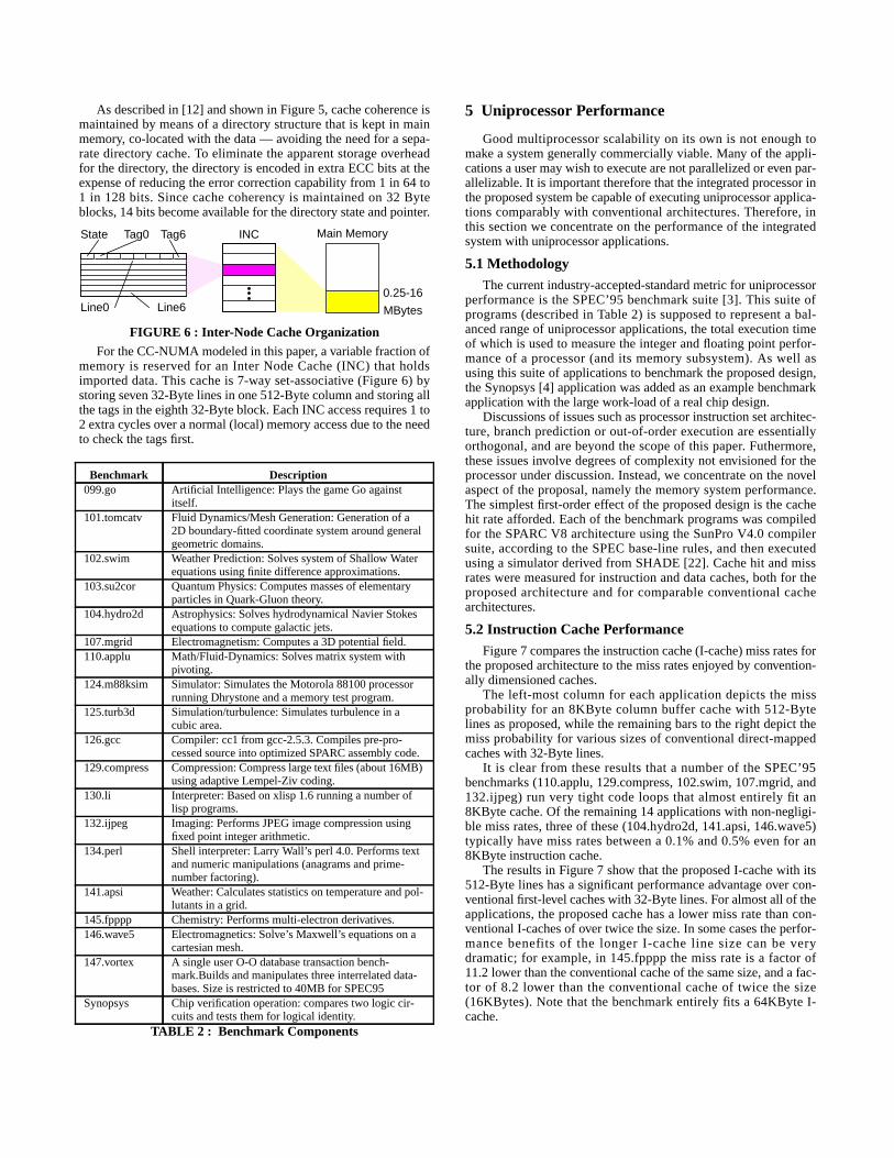
As described in [12] and shown in Figure 5, cache coherence ismaintained by means of a directory structure that is kept in mainmemory, co-located with the data — avoiding the need for a sepa-rate directory cache. To eliminate the apparent storage overheadfor the directory, the directory is encoded in extra ECC bits at theexpense of reducing the error correction capability from 1 in 64 to1 in 128 bits. Since cache coherency is maintained on 32 Byteblocks, 14 bits become available for the directory state and pointer.
FIGURE 6 : Inter-Node Cache Organization
For the CC-NUMA modeled in this paper, a variable fraction ofmemory is reserved for an Inter Node Cache (INC) that holdsimported data. This cache is 7-way set-associative (Figure 6) bystoring seven 32-Byte lines in one 512-Byte column and storing allthe tags in the eighth 32-Byte block. Each INC access requires 1 to2 extra cycles over a normal (local) memory access due to the needto check the tags first.
5 Uniprocessor Performance
Good multiprocessor scalability on its own is not enough tomake a system generally commercially viable. Many of the appli-cations a user may wish to execute are not parallelized or even par-allelizable. It is important therefore that the integrated processor inthe proposed system be capable of executing uniprocessor applica-tions comparably with conventional architectures. Therefore, inthis section we concentrate on the performance of the integratedsystem with uniprocessor applications.
5.1 MethodologyThe current industry-accepted-standard metric for uniprocessor
performance is the SPEC’95 benchmark suite [3]. This suite ofprograms (described in Table 2) is supposed to represent a bal-anced range of uniprocessor applications, the total execution timeof which is used to measure the integer and floating point perfor-mance of a processor (and its memory subsystem). As well asusing this suite of applications to benchmark the proposed design,the Synopsys [4] application was added as an example benchmarkapplication with the large work-load of a real chip design.
Discussions of issues such as processor instruction set architec-ture, branch prediction or out-of-order execution are essentiallyorthogonal, and are beyond the scope of this paper. Futhermore,these issues involve degrees of complexity not envisioned for theprocessor under discussion. Instead, we concentrate on the novelaspect of the proposal, namely the memory system performance.The simplest first-order effect of the proposed design is the cachehit rate afforded. Each of the benchmark programs was compiledfor the SPARC V8 architecture using the SunPro V4.0 compilersuite, according to the SPEC base-line rules, and then executedusing a simulator derived from SHADE [22]. Cache hit and missrates were measured for instruction and data caches, both for theproposed architecture and for comparable conventional cachearchitectures.
5.2 Instruction Cache PerformanceFigure 7 compares the instruction cache (I-cache) miss rates for
the proposed architecture to the miss rates enjoyed by convention-ally dimensioned caches.
The left-most column for each application depicts the missprobability for an 8KByte column buffer cache with 512-Bytelines as proposed, while the remaining bars to the right depict themiss probability for various sizes of conventional direct-mappedcaches with 32-Byte lines.
It is clear from these results that a number of the SPEC’95benchmarks (110.applu, 129.compress, 102.swim, 107.mgrid, and132.ijpeg) run very tight code loops that almost entirely fit an8KByte cache. Of the remaining 14 applications with non-negligi-ble miss rates, three of these (104.hydro2d, 141.apsi, 146.wave5)typically have miss rates between a 0.1% and 0.5% even for an8KByte instruction cache.
The results in Figure 7 show that the proposed I-cache with its512-Byte lines has a significant performance advantage over con-ventional first-level caches with 32-Byte lines. For almost all of theapplications, the proposed cache has a lower miss rate than con-ventional I-caches of over twice the size. In some cases the perfor-mance benefits of the longer I-cache line size can be verydramatic; for example, in 145.fpppp the miss rate is a factor of11.2 lower than the conventional cache of the same size, and a fac-tor of 8.2 lower than the conventional cache of twice the size(16KBytes). Note that the benchmark entirely fits a 64KByte I-cache.
Benchmark Description099.go Artificial Intelligence: Plays the game Go against
itself.101.tomcatv Fluid Dynamics/Mesh Generation: Generation of a
2D boundary-fitted coordinate system around generalgeometric domains.
102.swim Weather Prediction: Solves system of Shallow Waterequations using finite difference approximations.
103.su2cor Quantum Physics: Computes masses of elementaryparticles in Quark-Gluon theory.
104.hydro2d Astrophysics: Solves hydrodynamical Navier Stokesequations to compute galactic jets.
107.mgrid Electromagnetism: Computes a 3D potential field.110.applu Math/Fluid-Dynamics: Solves matrix system with
pivoting.124.m88ksim Simulator: Simulates the Motorola 88100 processor
running Dhrystone and a memory test program.125.turb3d Simulation/turbulence: Simulates turbulence in a
cubic area.126.gcc Compiler: cc1 from gcc-2.5.3. Compiles pre-pro-
cessed source into optimized SPARC assembly code.129.compress Compression: Compress large text files (about 16MB)
using adaptive Lempel-Ziv coding.130.li Interpreter: Based on xlisp 1.6 running a number of
lisp programs.132.ijpeg Imaging: Performs JPEG image compression using
fixed point integer arithmetic.134.perl Shell interpreter: Larry Wall’s perl 4.0. Performs text
and numeric manipulations (anagrams and prime-number factoring).
141.apsi Weather: Calculates statistics on temperature and pol-lutants in a grid.
145.fpppp Chemistry: Performs multi-electron derivatives.146.wave5 Electromagnetics: Solve’s Maxwell’s equations on a
cartesian mesh.147.vortex A single user O-O database transaction bench-
mark.Builds and manipulates three interrelated data-bases. Size is restricted to 40MB for SPEC95
Synopsys Chip verification operation: compares two logic cir-cuits and tests them for logical identity.
TABLE 2 : Benchmark Components
Line0
State Tag0
Line6
INCTag6 Main Memory
0.25-16
MBytes

The reduced miss rate of the proposed I-cache results directlyfrom the prefetching effect of the long cache line size, combinedwith the usually high degree of locality found in instructionstreams.
Conventional processor designs are unable to reap the benefitsof an increased cache line size because the time it takes to fill sucha line introduces second-order contention effects at the memoryinterface. The proposed integrated architecture fills the 512Byteline in a single cycle (after pre-charge and row access) directlyfrom the DRAM array, so these contention effects do not appear.We return to this issue of contention is again in Section 5.5.
Only two of the SPEC benchmarks stand out for their some-what disappointing I-cache performance; 134.perl has a surpris-ingly high miss rate, though still lower than the equivalentconventional cache of the same size, because the code is large andhas poor locality. 126.gcc has similar characteristics, but the I-cache miss rates for this application are within 27% of those of a64KByte conventional I-cache. Perhaps code profiling to reducecache conflicts may improve the miss rates for perl. The onlyapplication to produce a higher miss rate on the proposed architec-ture was 125.turb3d. This appears to be the result of a direct codeconflict between a loop and a function it calls, rather than a generalcapacity or locality problem. The problem is an artifact of thereduced number of cache lines, but can be removed by a code pro-filer noting the subroutine being called by the loop — the respec-tive loop and function code can then be re-laid by the compiler orlinker to avoid the conflict.
5.3 Data Cache PerformanceInstruction caches are important to keep the processor busy,
and the generally good locality of instruction streams means thatthe prefetching effect of the proposed cache works well. However,as the SPEC benchmarks show, even a modest size cache is suffi-cient to cover much of the executing code. Data caches, on the
other hand, need to cope with more complex access patterns inorder to be effective — often there is no substitute for cache capac-ity.
As described in Section 4.1, the proposed architecture hasthirty-two column buffers (each 512-Bytes long attached to each ofthe sixteen DRAM banks) dedicated to serving data accesses fromthe cpu, effectively making a 16KByte 2-way associative datacache (D-cache) with 512-Byte lines. This configuration was simu-lated in much the same way as the I-cache in order to compare itseffectiveness with direct mapped and 2-way associative first-levelcaches having a more conventional 32-Byte line size. Figure 8 pre-sents the miss rates resulting from these simulations. Each verticalbar shows both the load and the store cache miss probabilities —the combined height is the total cache-miss fraction. The bar to theleft for each application is the miss rate for the proposed D-cachestructure. The right-most bar for each application illustrates themiss rates after the addition of a small victim cache — we return tothis in Section 5.4. The remaining bars represent the conventionalcache miss rates.
Figure 8 shows that the application suite has a significantlymore varied D-cache than I-cache behavior. Given the generallyreduced temporal and spatial locality of data references comparedto instructions, this is to be expected. In turn, there is a more pro-nounced difference between the performance of the proposed D-cache structure and conventional cache designs for most of thebenchmarks.
Those applications that have a high degree of locality benefitfrom the prefetching effect of the long lines, but the long lines canalso increase the number of conflict misses. For example,107.mgrid and 104.hydro2d exhibit markedly reduced D-cachemiss rates — over a factor of ten lower for mgrid on the proposedarchitecture compared to a conventional direct-mapped D-cache ofthe same capacity, and still a factor of 5 lower than a 2-way asso-ciative 256KByte conventional cache configuration.
P P P P P P P P P PA A A A A A A A A AB B B B B B B B B BC C C C C C C C C CD D D D D D D D D D0.000
0.005
0.010
0.015
Pro
b. o
f ca
che
mis
s110.applu 129.compress 102.swim 107.mgrid 132.ijpeg 104.hydro2d 146.wave5 141.apsi 125.turb3d 130.li
Key:P - Proposed 8KB cache with 512B linesA - Conventional direct mapped 8KB cache with 32B linesB - 16KB direct mapped cache with 32B linesC - 64KB direct mapped cache with 32B linesD - 256KB direct mapped cache with 32B lines
P P P P P P P P PA A A A A A A A AB B B B B B B B BC C C C C C C C CD D D D D D D D D0.00
0.02
0.04
0.06
0.08
Pro
b. o
f ca
che
mis
s
101.tomcatv 103.su2cor synopsys 124.m88ksim 099.go 134.perl 147.vortex 126.gcc 145.fpppp
FIGURE 7 : Instruction Cache Miss Rates

Key:
Store Misses
Load Misses
P - 16KB, 2way with 512BlnesA - 16KB, d-mapped, 32B linesB - 64KB, d-mapped, 32B linesC - 256KB, d-mapped, 32B linesD - 16KB, 2 way, 32B linesE - 64KB, 2 way, 32B linesF - 256KB, 2 way, 32B linesQ - 16KB, 2 way, 512B lines +
16 entry x 32B victim cache
Unfortunately, the reverse is true of other applications; for103.su2cor, 102.swim and 101.tomcatv the 512-Byte line size ofthe proposed cache increases the number of conflict misses byalmost a factor of five over a conventional cache of the same size.
Early design simulations gave unacceptable miss rates for onlyan 8KB direct-mapped cache with 512-Byte lines — partly due tothe reduced capacity, but mostly due to the conflicts arising fromhaving only 16 cache lines.
Introducing an additional data column buffer to each DRAMcell doubled the capacity of the architecture’s D-cache to16KBytes, and provided two-way associativity, which dramaticallyimproved the performance. While the prefetching benefits of thelarge D-cache lines are desirable, as can been seen from the missrates in Figure 8, the conflict misses caused by the long line sizecan be equally detrimental for other applications. It is desirable,therefore, to reduce the incidences of conflict without reducing the512B line size or increasing the cache capacity.
5.4 Adding a Victim CacheJouppi [18] showed that a small, fully-associative buffer (“victim
cache”) could be used to hold cache lines most recently evicted fromthe data cache. This buffer works to increase the effective associa-tivity of the cache in cases where the cache miss rate is dominatedby conflicts, reducing the number of main memory accesses.
To reduce the dominating effect of cache conflicts seen inSection 5.3 for certain of the benchmark programs, a small asso-ciative victim cache was added, as proposed.
The entire buffer is the same size as a single cache line, thoughit is organized as a 16-way fully associative bank of 32-Byte lines.When a cache line is evicted from a DRAM column buffer, due toa miss, the last accessed 32-Byte sub-block of that line is copiedinto a selected entry in the victim cache before the new cache lineis read. This has no performance penalty, since the CPU is frozenon the miss, and the new cache line cannot be loaded until theaccess of the DRAM array completes. This leaves four free cyclesduring which to copy the 32-Byte sub-block from the old cacheline into the victim cache (64-bits at a time).
P P P P P P PA A A A A A AB B B B B B BC C C C C C CD D D D D D DE E E E E E EF F F F F F FQ Q Q Q Q Q Q0.00
0.01
0.02
0.03
0.04
0.05
0.06
Pro
b. o
f ca
che
mis
s124.m88ksim 132.ijpeg 130.li 107.mgrid 126.gcc 147.vortex 145.fpppp
P P P P P P PA A A A A A AB B B B B B BC C C C C C CD D D D D D DE E E E E E EF F F F F F FQ Q Q Q Q Q Q0.00
0.05
0.10
0.15
0.20
Pro
b. o
f ca
che
mis
s
134.perl 110.applu synopsys 125.turb3d 141.apsi 129.compress 104.hydro2d
P P P P PA A A A AB B B B BC C C C CD D D D DE E E E EF F F F FQ Q Q Q Q0.00
0.05
0.10
0.15
0.20
0.25
0.30
Pro
b. o
f ca
che
mis
s
099.go 146.wave5 103.su2cor 101.tomcatv 102.swim
FIGURE 8 : Data Cache Miss Rates
On each memory access cycle, as the main D-cache issearched, each of the 16 entries in the victim cache are alsochecked to see if it holds the data to be accessed. Unlike a conven-tional victim cache, the contents cannot be reloaded into a line ofthe main D-cache because of the size disparity.
The addition of the victim cache was simulated, and the result-ant miss rates collected and presented in the right-most result barsfor each application in Figure 8. A least-recently-used replacementalgorithm used for the entries in the victim cache.
The victim cache had a dramatic effect on the cache miss rates.In all but one application the combined D-cache and victim cachehas a lower miss rate than the 16KByte direct-mapped data cache.For the applications where the plain D-cache performed poorly(particularly 103.su2cor and 101.tomcatv), the victim cacheabsorbed the conflict misses reducing the miss rate to approxi-mately that of a conventional 2-way 16KByte cache. Moreover, forthree other applications (102.swim, 146.wave5, 130.li) the missrate was reduced between two and five-fold to a level equivalent toa 64KByte conventional cache. For 102.swim and 146.wave5 the2-way associative 16KByte D-cache has a slightly higher miss ratethan the direct-mapped one. It appears that for these applications ahigh degree of associativity is needed when the D-cache is small.The victim cache provides this associativity — absorbing theaccesses with poor spatial locality, and leaving the remainingaccesses to benefit from the prefetching effect of the longer cachelines. Hence, the miss rates are almost as low as for the 64KByteconventional caches.
There are always exceptions: while the victim cache helpsreduce the miss rate by 25%, it does not have the capacity toabsorb the conflicts from the main D-cache whose long lines arenot suited to the poor locality and small data structures used by the099.Go search algorithm.
In summary, the long lines of the column buffer based D-cacheprovide a beneficial prefetching effect for some applications, butalso cause significant cache conflicts for others due to the reducednumber of lines in the cache. A modest victim cache the size of asingle column buffer can absorb nearly all of the poor localitymisses and in some cases allow the prefetching effect to be seen.
5.5 Modeling Memory ContentionAlthough the column buffers comprising the data and instruc-
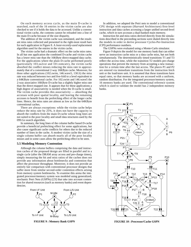
tion caches of the proposed design are filled in parallel and in asingle cycle (after the DRAM array access and pre-charge times),simply measuring the hit and miss ratios of the caches does notprovide any information about bottlenecks and contention thataffect the processor throughput. Moreover, it does not provide anentirely fair comparison with conventional processor designs thatsuffer more from similar second-order contention effects arisingfrom memory system bottlenecks. To examine this arena the inte-grated processor/memory system was modeled using generalized,stochastic Petri Nets (GSPNs) [23] that take into account conten-tion for shared resources (such as memory banks) and event depen-dencies.
FIGURE 9 : Memory Bank GSPN
In addition, we adapted the Petri nets to model a conventionalCPU design with separate (Harvard Architecture) first-levelinstruction and data caches accessing a larger unified second-levelcache, which in turn accesses a dual-banked main memory.
Instruction hit and miss ratios derived directly from the simula-tions described in the preceeding sections were dialed directly intothe models in order to derive processor Cycles-Per-Instruction(CPI) performance numbers.
The GSPNs were evaluated using a Monte-Carlo simulator.Figure 9 depicts the model for one memory bank that can either
serve an instruction cache miss or a data cache miss, but not bothsimultaneously. The deterministically timed transitions T1 and T3reflect the access time, while the transition T2 models pre-chargeoperations that prevent the memory from accepting a new transac-tion for a certain time after the last access. The places P1 and P2are entered via immediate transitions from the instruction fetchunit or the load/store unit. It is assumed that these transitions haveequal rates, so that memory banks are accessed with a uniform,random distribution. For the integrated processor/memory system,16 memory banks are used. The conventional reference systemwhich is used to validate the model has 2 independent memorybanks.
FIGURE 10 : Processor/Cache GSPN
From L/S UnitFrom I-F Unit
T1T2
T3
M-Idle
M-Busy
P1 P2
To L/S UnitTo I-F Unit
P1
P2
P3P4
P5
P6
P7
P8P9
A
A
B
B
P10
P11
P12 P13P14
P15 P16
T4
T5 T6
T7T8
T9
T10 T11
T12
P17 P18
P19
P20
T13
T14T15 T16
T17
T18T19
I-Mem
D-Mem
T20 T21 T22
T1
T2
T3
T23
T24
P21
T25
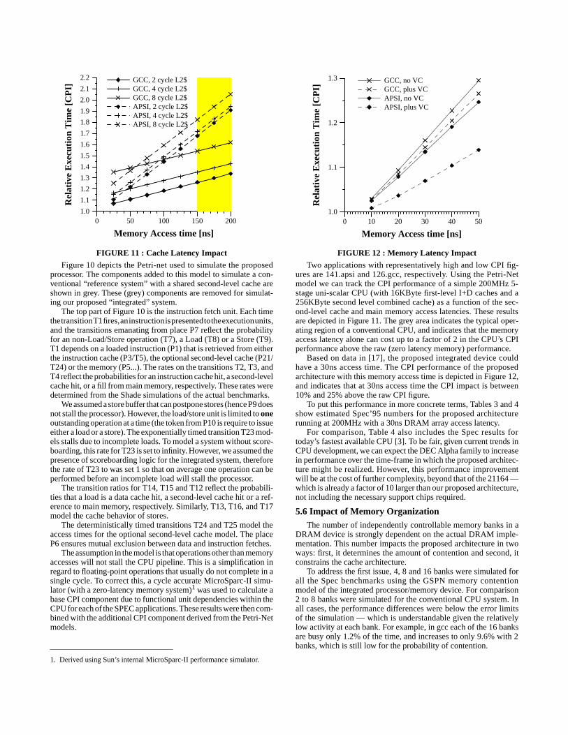
FIGURE 11 : Cache Latency Impact
Figure 10 depicts the Petri-net used to simulate the proposedprocessor. The components added to this model to simulate a con-ventional “reference system” with a shared second-level cache areshown in grey. These (grey) components are removed for simulat-ing our proposed “integrated” system.
The top part of Figure 10 is the instruction fetch unit. Each timethe transition T1 fires, an instruction is presented to the execution units,and the transitions emanating from place P7 reflect the probabilityfor an non-Load/Store operation (T7), a Load (T8) or a Store (T9).T1 depends on a loaded instruction (P1) that is retrieved from eitherthe instruction cache (P3/T5), the optional second-level cache (P21/T24) or the memory (P5...). The rates on the transitions T2, T3, andT4 reflect the probabilities for an instruction cache hit, a second-levelcache hit, or a fill from main memory, respectively. These rates weredetermined from the Shade simulations of the actual benchmarks.
We assumed a store buffer that can postpone stores (hence P9 doesnot stall the processor). However, the load/store unit is limited to oneoutstanding operation at a time (the token from P10 is require to issueeither a load or a store). The exponentially timed transition T23 mod-els stalls due to incomplete loads. To model a system without score-boarding, this rate for T23 is set to infinity. However, we assumed thepresence of scoreboarding logic for the integrated system, thereforethe rate of T23 to was set 1 so that on average one operation can beperformed before an incomplete load will stall the processor.
The transition ratios for T14, T15 and T12 reflect the probabili-ties that a load is a data cache hit, a second-level cache hit or a ref-erence to main memory, respectively. Similarly, T13, T16, and T17model the cache behavior of stores.
The deterministically timed transitions T24 and T25 model theaccess times for the optional second-level cache model. The placeP6 ensures mutual exclusion between data and instruction fetches.
The assumption in the model is that operations other than memoryaccesses will not stall the CPU pipeline. This is a simplification inregard to floating-point operations that usually do not complete in asingle cycle. To correct this, a cycle accurate MicroSparc-II simu-lator (with a zero-latency memory system)1 was used to calculate abase CPI component due to functional unit dependencies within theCPU for each of the SPEC applications. These results were then com-bined with the additional CPI component derived from the Petri-Netmodels.
1. Derived using Sun’s internal MicroSparc-II performance simulator.
FIGURE 12 : Memory Latency Impact
Two applications with representatively high and low CPI fig-ures are 141.apsi and 126.gcc, respectively. Using the Petri-Netmodel we can track the CPI performance of a simple 200MHz 5-stage uni-scalar CPU (with 16KByte first-level I+D caches and a256KByte second level combined cache) as a function of the sec-ond-level cache and main memory access latencies. These resultsare depicted in Figure 11. The grey area indicates the typical oper-ating region of a conventional CPU, and indicates that the memoryaccess latency alone can cost up to a factor of 2 in the CPU’s CPIperformance above the raw (zero latency memory) performance.
Based on data in [17], the proposed integrated device couldhave a 30ns access time. The CPI performance of the proposedarchitecture with this memory access time is depicted in Figure 12,and indicates that at 30ns access time the CPI impact is between10% and 25% above the raw CPI figure.
To put this performance in more concrete terms, Tables 3 and 4show estimated Spec’95 numbers for the proposed architecturerunning at 200MHz with a 30ns DRAM array access latency.
For comparison, Table 4 also includes the Spec results fortoday’s fastest available CPU [3]. To be fair, given current trends inCPU development, we can expect the DEC Alpha family to increasein performance over the time-frame in which the proposed architec-ture might be realized. However, this performance improvementwill be at the cost of further complexity, beyond that of the 21164 —which is already a factor of 10 larger than our proposed architecture,not including the necessary support chips required.
5.6 Impact of Memory OrganizationThe number of independently controllable memory banks in a
DRAM device is strongly dependent on the actual DRAM imple-mentation. This number impacts the proposed architecture in twoways: first, it determines the amount of contention and second, itconstrains the cache architecture.
To address the first issue, 4, 8 and 16 banks were simulated forall the Spec benchmarks using the GSPN memory contentionmodel of the integrated processor/memory device. For comparison2 to 8 banks were simulated for the conventional CPU system. Inall cases, the performance differences were below the error limitsof the simulation — which is understandable given the relativelylow activity at each bank. For example, in gcc each of the 16 banksare busy only 1.2% of the time, and increases to only 9.6% with 2banks, which is still low for the probability of contention.
0 50 100 150 200
Memory Access time [ns]
1.0
1.1
1.2
1.3
1.4
1.5
1.6
1.7
1.8
1.9
2.0
2.1
2.2R
elat
ive
Exe
cuti
on T
ime
[CP
I]GCC, 2 cycle L2$GCC, 4 cycle L2$GCC, 8 cycle L2$APSI, 2 cycle L2$APSI, 4 cycle L2$APSI, 8 cycle L2$
0 10 20 30 40 50
Memory Access time [ns]
1.0
1.1
1.2
1.3
Rel
ativ
e E
xecu
tion
Tim
e [C
PI]
GCC, no VCGCC, plus VCAPSI, no VCAPSI, plus VC

The second and much larger effect is the impact upon practicalcache organization. If the number of banks were to be reduced, eitherthe line size or the associativity of the cache needs to be increased.Mitsubishi [9] opted to use 4 banks and add a small amount ofSRAM to each bank to increase the number of available lines. In thiscase, the cache organization essentially remains unchanged and theoverall performance only decreases slightly due to some increase incontention. However, simulation shows that increasing the line sizewill degrade performance due to higher resultant cache conflicts.
6 Multiprocessor Performance
Thus far, only the uniprocessor performance of the proposed inte-grated system has been considered. The unusual design of the pro-cessor caches was shown, in most cases, to be beneficial, but it is notclear that this should be the case for shared memory multiprocessingwhere the addition of coherence misses affects the caches.
6.1 Simulation Models and MethodologyTo understand the performance potential of the integrated
design, an execution driven simulation, with a timing-accuratearchitecture model, was used to evaluate a simple system based onthe building blocks of Figure 3. These performance figures arethen compared with results obtained from a reference CC-NUMAdesign [20] with 16KByte direct-mapped First-Level Caches(FLCs) and infinitely sized Second-Level Caches (SLCs). The useof infinite SLCs removes the SLC capacity misses, providing anideal upper-bound of the system performance when only the coldand the coherence misses are considered [24]. This enables thedirect study of the integrated cache system compared to a conven-tional FLC in a shared memory system.
To simulate the proposed integrated system, the Inter-NodeCache (INC) size was set at 1MByte per memory/processor node— larger than the working sets of the applications used, and socomparable to the infinite SLCs of the reference CC-NUMA archi-tecture. However, a finite size was chosen because the INCs areconfigured as 7-way set-associative caches; making them infinitelylarge would remove the beneficial effects of set associativity. Thegranularity of coherence (or coherence unit) is always 32-Bytes.For the purposes of these simulations, cache coherence was main-tained by a write-invalidate protocol [24].
The simulation benchmarks are taken from the SPLASH [25]suite, for which brief descriptions and the sizes of the data setsused are given in Table 5.
The architectural simulator is built on top of the CacheMireTest Bench [26], which is an execution-driven simulator of multi-ple SPARC processors. The processors in the CacheMire simulatorissue memory accesses, and the architectural simulator then delaysthe processors according to the latencies shown in Table 6. TheSPLASH application codes are sufficiently small that for both theintegrated and the reference architectures, instruction fetches areassumed to always hit in the instruction caches. Therefore, onlydata references were simulated.
NameCPI
[cpu + memory] Spec-ratio099.go 1.01 + 0.48 6.0124.m88ksim 1.01 + 0.12 4.3126.gcc 1.01 + 0.14 7.6129.compress 1.03 + 0.17 6.4130.li 1.02 + 0.06 6.7132.ijpeg 1.00 + 0.01 5.8134.perl 1.04 + 0.21 6.0147.vortex 1.02 + 0.27 6.4
101.tomcatv 1.15 + 0.50 8.2102.swim 1.56 + 0.97 12.7103.su2cor 1.41 + 0.44 3.2104.hydro2d 1.74 + 0.04 4.2107.mgrid 1.20 + 0.01 3.2110.applu 1.53 + 0.01 3.9125.turb3d 1.16 + 0.05 4.3141.apsi 1.70 + 0.08 5.0145.fpppp 1.34 + 0.08 7.5146.wave5 1.31 + 0.25 7.6
TABLE 3 : Spec’95 Estimates, no Victim Cache
Name Total CPI Spec-ratioAlpha 21164
[DEC 8200 5/300]099.go 1.30 6.9 10.1124.m88ksim 1.10 4.5 7.1126.gcc 1.13 7.8 6.7129.compress 1.16 6.6 6.8130.li 1.07 6.8 6.8132.ijpeg 1.01 5.8 6.9134.perl 1.21 6.2 8.1147.vortex 1.17 7.1 7.4
101.tomcatv 1.23 11.1 14.0102.swim 1.65 19.5 18.3103.su2cor 1.51 3.9 7.2104.hydro2d 1.75 4.2 7.8107.mgrid 1.21 3.2 9.1110.applu 1.54 4.0 6.5125.turb3d 1.20 4.3 10.8141.apsi 1.76 5.1 14.5145.fpppp 1.42 7.5 21.3146.wave5 1.41 8.4 16.8
TABLE 4 : Spec’95 Estimates, with Victim Cache
Benchmark Description Data SetLU LU decomposition 200x200 matrixMP3D 3-D particle-based wind-
tunnel simulator10 K particles, 10 steps
Ocean Ocean basin simulator 128x128 grids, tolerance 10-7
Water N-body water moleculardynamics simulation
288 molecules, 4 time steps
PTHOR Distributed digital timedigital circuit simulator
RISC circuit, 1000 time steps
TABLE 5 : Splash Benchmarks
System Access LatencyProposedCombined
CPU &DRAM
Hit in column buffer 1Hit in victim cache 1Access local memory & INC 6Invalidation round trip delay 80Load remote data 80
ComparativeCC-NUMA
Hit in FLC 1Hit in SLC 6Invalidation round trip delay 80Load remote data 80
TABLE 6 : Memory Latency (processor cycles)

6.2 Performance ResultsThe total execution times with increasing numbers of proces-
sors for the benchmarks LU, MP3D, OCEAN, WATER andPTHOR are depicted in Figures 13 to 17.
The column buffers, which load 512-Bytes at a time, exploit thespatial locality of local memory accesses well due to the long-lineprefetching effect mentioned earlier. As a result, the integrateddesign outperforms the traditional CC-NUMA designs for smallnumbers of processors in all cases — until the working set per cpubecomes too small for the effect to be observed.
Since the coherence units transferred between nodes are always32-Byte blocks, the long-line prefetching effect does not help foraccesses to data held on another node. Therefore the proposedarchitecture has the same number of cold and coherence misses asthe traditional CC-NUMA. In fact, it is important not to use thelong cache lines as coherence units, because the false-sharing costswould outweigh the prefetching benefits for most applications.However, the long cache lines can improve the performance of theintegrated multiprocessor’s remote data caches. The long columnbuffer lines enable access to seven 32-Byte INC blocks each - pro-viding 7 way associativity for cached remote memory reducingconflict misses.
When applications exhibit good locality for local memoryaccesses or have a large number of conflicts on remote dataaccesses, the proposed column buffer design can produce goodresults. WATER is the only benchmark for which the reference
CC-NUMA design shows better results than the integrated archi-tecture unaided by a victim cache. In WATER, the main data struc-ture is a shared vector that maintains all molecules. Sets ofmolecules are allocated to processors statically. In this application,true sharing misses dominate. As each molecule is described by adata structure of approximately 600 Bytes, and is only partiallyaccessed, the limited numbers of column buffers of 512-Bytes suf-fer from the lack of spatial and temporal locality. As shown inFigure 16, when the victim caches are used, the total executiontime is significantly reduced.
A further observation is that the column buffer D-cache itself isnot enough to support scalable computation. As shown inFigures 15 and 16, the reference CC-NUMA performs better thanthe integrated design with only column buffers. Again, this isbecause the addition of coherence traffic from shared memoryoperation further increases the conflict misses caused by the smallnumber of column buffer long lines. As a result, most memoryaccesses miss the D-cache and need 6 cycles to reach the data inthe INC DRAM in the integrated design; while similar accessesmay be served in 1 cycle by the FLC of the reference CC-NUMAdesign. This is not quite a fair comparison due to the small natureof the standard problems’ working sets — with larger, more realis-tic, problems, the FLC of the reference CC-NUMA architecturewould start experiencing more capacity misses, incurring the 6cycle penalty to it's SLC.
Based on preliminary observations, each node in the integrateddesign was augmented just as in the uniprocessor case by the addi-
FIGURE 14 : MP3D FIGURE 15 : OCEAN
FIGURE 16 : WATER FIGURE 17 : PTHOR
FIGURE 13 : LU
1 2 4 8 12 16Number of cpus
0
10
20
30
40
50
Tim
e (m
illio
ns o
f cp
u cy
cles
)
1 2 4 8 12 16Number of cpus
0
5
10
15
20
Tim
e (m
illio
ns o
f cp
u cy
cles
)
1 2 4 8 12 16Number of cpus
0
100
200
300
400
500
Tim
e (m
illio
ns o
f cp
u cy
cles
)1 2 4 8 12 16
Number of cpus
0
200
400
600
Tim
e (m
illio
ns o
f cp
u cy
cles
)
1 2 4 8 12 16Number of cpus
0
50
100
150
200
Tim
e (m
illio
ns o
f cp
u cy
cles
) Key:
CC-NUMA
Without victim cache
With victim cache

tion of a small 16-way by 32-Byte associative victim cache. Com-pared to the 16KByte FLC of the reference CC-NUMA, the 512-Byte capacity of the victim cache is very small, however even thiscan reduce the execution time of the integrated design by up to afactor of 2 (in the case of WATER). With the aid of a victim cache,the integrated design shows the best performance results for thetested applications.
7 Related Work
TransputerIn 1982 Inmos introduced the Transputer family of RISC pro-
cessor chips [27] that were combined with a small amount of localmemory and tightly integrated with a 4 serial link communicationsinterface. The processor was tailored for a message-passing para-digm (specifically, the language Occam), and efficiently supportedhigh speed context switching and message handling. While thischip has some similarities with the idea presented it did not pro-vide a shared memory capability or even virtual memory. More-over, the local memory was simply 1KB of static RAM, so for allpractical applications the chip had to be combined with externalDRAM.
M machineThe M-Machine [28] project plans to integrate 4 super-scalar
CPUs with memory on a single chip. However, the on-chip mem-ory size is small as 4Mbits. In most cases, external I/O and mem-ory chips are needed. Moreover, the M-Machine is a messagepassing design.
ExacubeThe EXECUBE [29] exploited a similar idea of utilizing the
memory bandwidth to the maximum by CPU memory integration.A CPU element, 64KBytes of memory and four communicationlinks form a processing unit. Each chip, based on the dense DRAMtechnology of the day, holds eight such processing units. Unlikeour design, the EXECUBE chip is intended to serve as buildingblock for MPP systems. There is no shared memory capability, orability to use DRAM column buffers for instruction and datacaches. Furthermore, it is primarily intended as a SIMD architec-ture.
SharcThe Analog Devices ADSP-21060 chip [30] has a single DSP
(digital signal processor) CPU integrated with 4Mbits of memory.Like the EXECUBE, MPPs systems can also be built using thischip, but not shared-memory systems.
Mitsubishi, Toshiba & NECMitsubishi have already fabricated a combined 32-bit RISC
core and DRAM device [9]. While this device demonstrates that acommercial DRAM process can be used to fabricate complex logicon the same chip, it contained a conventional cache design sepa-rated from the DRAM arrays, thus failing to exploit the full mem-ory bandwidth potential. Futhermore, the device contains noscalable interconnect capability.
Other DRAM vendors, for example Toshiba and NEC, are inthe process of making available DRAM devices with dedicatedsemi-custom logic areas, so that customers can design their ownintelligent DRAMs.
8 Vision
The integrated processor/memory chip could be regarded as theequivalent to a LegoTM building block. Dwarfed by its modestheat-sink to cool some 1.5W, the processing elements could beadded incrementally to a silicon-less mother board (Figure 20) thatprovides only sockets with power and signal traces to other suchsockets. When needed, more integrated chips can be added to alogically seamless shared memory multiprocessor.
FIGURE 18 : Silicon-Less Motherboard
I/O functions are handled by chips that can translate to standardinterfaces, such as PCI, SCSI, ATM, Fiber-Channel, etc. Amongthe more interesting capabilities of such a system is to build aframebuffer that retrieves its data from the main memory as itrefreshes a screen or LCD panel. This is made feasible by the highmemory bandwidth that is available internally.
Due to the scalable interconnect fabric, the system’s bi-sec-tional bandwidth increases as components are added. This systemis not limited to one mother-board, rather the delay insensitivepoint-to-point connections of the S-Connect systems allow multi-ple boards to communicate via cables (<10m) or fiber-optic con-nections (up to 200m).
9 Conclusions
The trend towards larger DRAM devices exacerbates the pro-cessor/memory bottleneck, requiring costly cache hierarchies toeffectively support high performance microprocessors. A viablealternative is to move the processor closer to the memory, by inte-grating it onto the DRAM chip. Processor/memory integration isadvantageous, even if it requires the use of a simpler processor.
We have shown that a conventional, single-scalar processorwith a small cache, integrated with a 256-Mbit DRAM array canform a self-contained, general purpose processing element withcompetitive performance that can approach that of high-end super-scalar processors with large, multilevel caches. Small (8KByte)direct mapped instruction caches with long lines (512-Bytes) per-form surprisingly well with a zero-fill cost, which is a feature ofthe integration. Victim caches were shown to be very effectivewhen combined with a multi-banked column buffer data cache.Combined with the lower latency inherent in an integrated design,the memory induced degradation of processor performance wasgreatly reduced.
Including scalable Distributed Shared Memory (DSM) withhardware assisted cache coherency results in a versatile buildingblock that can outperform an ideal (i.e. infinite second-level cache)conventional DSM system.
Motherboard
Processor/Memory Chip PCI+ Chip
SBus Chip
Mega I/O
Out-composing
ScalablePP-Interconnect
Base-I/O
Framebuffer

AcknowledgmentsThe authors would like to acknowledge the valuable help, feed-
back and inspiration they received from Gunes Aybay, ClementFang, Howard Davidson, Mark Hill, Sally McKee, William Radke,Eugen Schenfeld, Sanjay Vishin, the engineers of the Sparc Tech-nology Business organization and the reviewers.
References[1] Wulf, Wm.A and McKee, S.A. Hitting the Memory Wall:
Implications of the Obvious. ACM Computer ArchitectureNews. Vol.23, No.1 March 1995.
[2] Wilkes, M.V., The Memory Wall and the CMOS End-Point,ACM Computer Architecture News. Vol. 23, No. 4 September1995.
[3] SPEC Newsletter; URL: http://www.specbench.org/results.html
[4] Synopsys Inc., 700 East Middlefield Rd. Mountain View, Cali-fornia, CA 94043.
[5] Horiguchi, M. et.al., An Experimental 220MHz 1Gb DRAM,IEEE International Solid-State Circuits Conference 1995. SanFrancisco, p.252.
[6] Sugibayashi, T. et.al., A 1Gb DRAM for file Applications,IEEE International Solid-State Circuits Conference 1995. SanFrancisco, p.254.
[7] Miyano, S. et.al., A 1.6GB/s Data-Transfer-Rate 8Mb Embed-ded DRAM, IEEE International Solid-State Circuits Confer-ence 1995. San Francisco, p.300
[8] MicroSparc documentation, internal communication withSparc Technology Business Inc.
[9] Shimizu, et.al. A Multimedia 32b RISC Microprocessor with16Mb DRAM, International Solid-State-Circuits Conference,February 1996, pp216-217.
[10]MIPS R4300i Processor Reference Manual, URL: http://www.mips.com/r4300i/R4300i_B.html
[11]Nowatzyk, A., Browne, M., Kelly, E. and Parkin, M. S-Con-nect: from Network of Workstations to Supercomputer Perfor-mance. Proceedings of the 22nd International Symposium onComputer Architecture, June 1994.
[12]Nowatzyk, A., Aybay, G., Browne, M., Kelly, E., Parkin, M.,Radke, B. and Vishin, S. The S3.mp Scalable Shared MemoryMultiprocessor. Proceedings of the 24th International Confer-ence on Parallel Processing, 1995.
[13]MB81164840 - CMOS 4x2Mx8 Synchronous DRAM, FujitsuMicroelectronics Inc., 3455 N. first St., San Jose CA 95134,
[14]RDRAM Reference Manual, Rambus Inc., 2465 LathamStreet, Mountain View, CA 94040.
[15]Yoo, J.H. et.al., A 32-bank 1Gb DRAM with 1GB/s Bandwidth,IEEE International Solid-State Circuits Conference 1996, SanFrancisco, p.378.
[16]Przybylski, S., MoSys Reveals MDRAM Architecture, Micro-processor Report, Vol 9:17, Dec 25, 1995, MicroDesignResources, Sebastopol, CA95472. ISSN 0899-9341
[17]Koike, H., et.al., A 30ns 64Mb DRAM with Built-in Self-Testand Repair Function,ISSCC 1992, San Francisco, p150
[18]Jouppi, N. Improving Direct-Mapped Cache Performance byAddition of a Small Fully-Associative Cache and PrefetchBuffer, Proceedings of the 17th Annual International Sympo-sium on Computer Architecture, 1990 pages 364-373
[19]Nowatzyk, A., Aybay, G., Browne, M., Kelly, E., Parkin, M.,Radke, B. and Vishin, S.Exploiting Parallelism in CacheCoherency Protocol engines, Europar 1995, Stockholm, Swe-den
[20]Lenoski, D. The Design and Analysis of DASH: A ScalableDirectory-Based Multiprocessor. PhD Dissertation, StanfordUniversity, December 1991.
[21]Saulsbury, A. et.al. An Argument for Simple COMA, 1st IEEESymposium on High Performance Computer Architecture Jan-uary 22-25th 1995, Rayleigh, North Carolina, USA; pages276-285.
[22]Cmelik, B. The SHADE simulator, Sun-Labs TechnicalReport, 1993
[23]Marsan, G.,Conti, A class of generalized stochastic petrinetsfor the performance evaluation of multiprocessor systems,ACM Transactions on Computer Systems, 2(2): 93, May 1984
[24]Dubois, M., Skeppstedt, J., Ricciulli, L., Ramamurthy, K. andStenström, P. The Detection and Elimination of UselessMisses in Multiprocessors. Proceedings of the 20th AnnualInternational Symposium on Computer Architecture, pp. 88-97, May 1993.
[25]Singh, J.P., Weber, W.-D., and Gupta, A. SPLASH: StanfordParallel Applications for Shared-Memory. Computer Archi-tecture News, 20(1):5-44, March 1992.
[26]Brorsson, M., Dahlgren, F., Nilsson, H. and Stenström, P. TheCacheMire Test Bench - A Flexible and Effective Approach forSimulation of Multiprocessors. Proceedings of the 26thAnnual Simulation Symposium, pp. 115-124, 1993.
[27]The Transputer Reference Manual, 1988, INMOS Ltd., Pub.Prentice Hall, ISBN 0-13-929001-X.
[28]Dally, W.J. et. al. M-Machine Microarchitecture, Tech Report,Artificial Intelligence Lab MIT, Cambridge, MA. Jan 1993
[29]Kogge, P.M., EXECUBE - A New Architecture for ScalableMPPs, 1994 International Conference on Parallel Processing.
[30]ADSP-21060 SHARC Super Harvard Architecture Computer,ANALOG DEVICES, Norwood, MA, Oct. 1993.