Embed Size (px)
Citation preview
Document Number: MD00090Revision 3.12April 28, 2011
MIPS Technologies, Inc.955 East Arques Avenue
Sunnyvale, CA 94085-4521
Copyright © 2001-2003,2005,2008-2011 MIPS Technologies Inc. All rights reserved.
MIPSVerified
™
MIPS® Architecture For ProgrammersVolume III: The MIPS32® and
microMIPS32™ Privileged ResourceArchitecture

MIPS® Architecture For Programmers Volume III: The MIPS32® and microMIPS32™ Privileged Resource Architecture, Revi-sion 3.12
Copyright © 2001-2003,2005,2008-2011 MIPS Technologies Inc. All rights reserved.
Template: nB1.03, Built with tags: 2B ARCH MIPS32
Copyright © 2001-2003,2005,2008-2011 MIPS Technologies, Inc. All rights reserved.
Unpublished rights (if any) reserved under the copyright laws of the United States of America and other countries.
This document contains information that is proprietary to MIPS Technologies, Inc. ("MIPS Technologies"). Any copying, reproducing, modifying or use ofthis information (in whole or in part) that is not expressly permitted in writing by MIPS Technologies or an authorized third party is strictly prohibited. At aminimum, this information is protected under unfair competition and copyright laws. Violations thereof may result in criminal penalties and fines.
Any document provided in source format (i.e., in a modifiable form such as in FrameMaker or Microsoft Word format) is subject to use and distributionrestrictions that are independent of and supplemental to any and all confidentiality restrictions. UNDER NO CIRCUMSTANCES MAY A DOCUMENTPROVIDED IN SOURCE FORMAT BE DISTRIBUTED TO A THIRD PARTY IN SOURCE FORMAT WITHOUT THE EXPRESS WRITTENPERMISSION OF MIPS TECHNOLOGIES, INC.
MIPS Technologies reserves the right to change the information contained in this document to improve function, design or otherwise. MIPS Technologies doesnot assume any liability arising out of the application or use of this information, or of any error or omission in such information. Any warranties, whetherexpress, statutory, implied or otherwise, including but not limited to the implied warranties of merchantability or fitness for a particular purpose, are excluded.Except as expressly provided in any written license agreement from MIPS Technologies or an authorized third party, the furnishing of this document does notgive recipient any license to any intellectual property rights, including any patent rights, that cover the information in this document.
The information contained in this document shall not be exported, reexported, transferred, or released, directly or indirectly, in violation of the law of anycountry or international law, regulation, treaty, Executive Order, statute, amendments or supplements thereto. Should a conflict arise regarding the export,reexport, transfer, or release of the information contained in this document, the laws of the United States of America shall be the governing law.
The information contained in this document constitutes one or more of the following: commercial computer software, commercial computer softwaredocumentation or other commercial items. If the user of this information, or any related documentation of any kind, including related technical data or manuals,is an agency, department, or other entity of the United States government ("Government"), the use, duplication, reproduction, release, modification, disclosure,or transfer of this information, or any related documentation of any kind, is restricted in accordance with Federal Acquisition Regulation 12.212 for civilianagencies and Defense Federal Acquisition Regulation Supplement 227.7202 for military agencies. The use of this information by the Government is furtherrestricted in accordance with the terms of the license agreement(s) and/or applicable contract terms and conditions covering this information from MIPSTechnologies or an authorized third party.
MIPS, MIPS I, MIPS II, MIPS III, MIPS IV, MIPS V, MIPS-3D, MIPS16, MIPS16e, MIPS32, MIPS64, MIPS-Based, MIPSsim, MIPSpro, MIPS Technologieslogo, MIPS-VERIFIED, MIPS-VERIFIED logo, 4K, 4Kc, 4Km, 4Kp, 4KE, 4KEc, 4KEm, 4KEp, 4KS, 4KSc, 4KSd, M4K, M14K, 5K, 5Kc, 5Kf, 24K, 24Kc,24Kf, 24KE, 24KEc, 24KEf, 34K, 34Kc, 34Kf, 74K, 74Kc, 74Kf, 1004K, 1004Kc, 1004Kf, R3000, R4000, R5000, ASMACRO, Atlas, "At the core of theuser experience.", BusBridge, Bus Navigator, CLAM, CorExtend, CoreFPGA, CoreLV, EC, FPGA View, FS2, FS2 FIRST SILICON SOLUTIONS logo, FS2NAVIGATOR, HyperDebug, HyperJTAG, JALGO, Logic Navigator, Malta, MDMX, MED, MGB, microMIPS, OCI, PDtrace, the Pipeline, Pro Series, SEAD,SEAD-2, SmartMIPS, SOC-it, System Navigator, and YAMON are trademarks or registered trademarks of MIPS Technologies, Inc. in the United States andother countries.
All other trademarks referred to herein are the property of their respective owners.
MIPS® Architecture For Programmers Volume III: The MIPS32® and microMIPS32™ Privileged Resource Architecture, Revi-sion 3.12 3
Copyright © 2001-2003,2005,2008-2011 MIPS Technologies Inc. All rights reserved.
Contents
Chapter 1: About This Book ................................................................................................................ 111.1: Typographical Conventions ....................................................................................................................... 11
1.1.1: Italic Text.......................................................................................................................................... 111.1.2: Bold Text .......................................................................................................................................... 121.1.3: Courier Text ..................................................................................................................................... 12
1.2: UNPREDICTABLE and UNDEFINED ....................................................................................................... 121.2.1: UNPREDICTABLE........................................................................................................................... 121.2.2: UNDEFINED .................................................................................................................................... 131.2.3: UNSTABLE ...................................................................................................................................... 13
1.3: Special Symbols in Pseudocode Notation................................................................................................. 131.4: For More Information ................................................................................................................................. 16
Chapter 2: The MIPS32 and microMIPS32 Privileged Resource Architecture ................................ 172.1: Introduction................................................................................................................................................ 172.2: The MIPS Coprocessor Model .................................................................................................................. 17
2.2.1: CP0 - The System Coprocessor ...................................................................................................... 172.2.2: CP0 Registers .................................................................................................................................. 17
Chapter 3: MIPS32 and microMIPS32 Operating Modes................................................................... 193.1: Debug Mode ............................................................................................................................................. 193.2: Kernel Mode .............................................................................................................................................. 193.3: Supervisor Mode ....................................................................................................................................... 193.4: User Mode ................................................................................................................................................. 203.5: Other Modes.............................................................................................................................................. 20
3.5.1: 64-bit Floating Point Operations Enable .......................................................................................... 203.5.2: 64-bit FPR Enable............................................................................................................................ 203.5.3: Coprocessor 0 Enable...................................................................................................................... 213.5.4: ISA Mode ......................................................................................................................................... 21
Chapter 4: Virtual Memory ................................................................................................................... 234.1: Differences between Releases of the Architecture.................................................................................... 23
4.1.1: Virtual Memory ................................................................................................................................. 234.1.2: Protection of Virtual Memory Pages................................................................................................. 234.1.3: Context Register .............................................................................................................................. 23
4.2: Terminology............................................................................................................................................... 244.2.1: Address Space................................................................................................................................. 244.2.2: Segment and Segment Size ............................................................................................................ 244.2.3: Physical Address Size (PABITS) ..................................................................................................... 24
4.3: Virtual Address Spaces ............................................................................................................................. 254.4: Compliance................................................................................................................................................ 274.5: Access Control as a Function of Address and Operating Mode................................................................ 284.6: Address Translation and Cacheability & Coherency Attributes for the kseg0 and kseg1 Segments ........ 284.7: Address Translation for the kuseg Segment when StatusERL = 1 ............................................................. 294.8: Special Behavior for the kseg3 Segment when DebugDM = 1................................................................... 294.9: TLB-Based Virtual Address Translation .................................................................................................... 29
4.9.1: Address Space Identifiers (ASID) .................................................................................................... 30
4MIPS® Architecture For Programmers Volume III: The MIPS32® and microMIPS32™ Privileged Resource Architecture, Revi-sion 3.12
Copyright © 2001-2003,2005,2008-2011 MIPS Technologies Inc. All rights reserved.
4.9.2: TLB Organization ............................................................................................................................. 304.9.3: TLB Initialization............................................................................................................................... 314.9.4: Address Translation ......................................................................................................................... 32
Chapter 5: Common Device Memory Map.......................................................................................... 395.1: CDMMBase Register................................................................................................................................. 395.2: CDMM - Access Control and Device Register Blocks ............................................................................... 40
5.2.1: Access Control and Status Registers............................................................................................... 41
Chapter 6: Interrupts and Exceptions................................................................................................. 436.1: Interrupts ................................................................................................................................................... 43
6.1.1: Interrupt Modes ................................................................................................................................ 446.1.2: Generation of Exception Vector Offsets for Vectored Interrupts ...................................................... 53
6.2: Exceptions ................................................................................................................................................. 556.2.1: Exception Priority ............................................................................................................................. 556.2.2: Exception Vector Locations.............................................................................................................. 576.2.3: General Exception Processing......................................................................................................... 596.2.4: EJTAG Debug Exception ................................................................................................................. 616.2.5: Reset Exception ............................................................................................................................... 626.2.6: Soft Reset Exception........................................................................................................................ 636.2.7: Non Maskable Interrupt (NMI) Exception ........................................................................................ 646.2.8: Machine Check Exception................................................................................................................ 656.2.9: Address Error Exception .................................................................................................................. 656.2.10: TLB Refill Exception....................................................................................................................... 666.2.11: Execute-Inhibit Exception............................................................................................................... 676.2.12: Read-Inhibit Exception ................................................................................................................... 676.2.13: TLB Invalid Exception .................................................................................................................... 686.2.14: TLB Modified Exception ................................................................................................................. 696.2.15: Cache Error Exception ................................................................................................................... 696.2.16: Bus Error Exception ....................................................................................................................... 706.2.17: Integer Overflow Exception ............................................................................................................ 706.2.18: Trap Exception ............................................................................................................................... 716.2.19: System Call Exception ................................................................................................................... 716.2.20: Breakpoint Exception ..................................................................................................................... 716.2.21: Reserved Instruction Exception ..................................................................................................... 726.2.22: Coprocessor Unusable Exception.................................................................................................. 726.2.23: Floating Point Exception ................................................................................................................ 736.2.24: Coprocessor 2 Exception ............................................................................................................... 736.2.25: Watch Exception ............................................................................................................................ 746.2.26: Interrupt Exception ......................................................................................................................... 74
Chapter 7: GPR Shadow Registers ..................................................................................................... 777.1: Introduction to Shadow Sets...................................................................................................................... 777.2: Support Instructions................................................................................................................................... 78
Chapter 8: CP0 Hazards ....................................................................................................................... 798.1: Introduction................................................................................................................................................ 798.2: Types of Hazards ...................................................................................................................................... 79
8.2.1: Possible Execution Hazards ............................................................................................................ 798.2.2: Possible Instruction Hazards............................................................................................................ 81
8.3: Hazard Clearing Instructions and Events .................................................................................................. 828.3.1: MIPS32 Instruction Encoding........................................................................................................... 82
MIPS® Architecture For Programmers Volume III: The MIPS32® and microMIPS32™ Privileged Resource Architecture, Revi-sion 3.12 5
Copyright © 2001-2003,2005,2008-2011 MIPS Technologies Inc. All rights reserved.
8.3.2: microMIPS32 Instruction Encoding .................................................................................................. 83
Chapter 9: Coprocessor 0 Registers .................................................................................................. 859.1: Coprocessor 0 Register Summary ............................................................................................................ 859.2: Notation ..................................................................................................................................................... 909.3: Writing CPU Registers............................................................................................................................... 919.4: Index Register (CP0 Register 0, Select 0)................................................................................................. 929.5: Random Register (CP0 Register 1, Select 0)............................................................................................ 939.6: EntryLo0, EntryLo1 (CP0 Registers 2 and 3, Select 0) ............................................................................. 949.7: Context Register (CP0 Register 4, Select 0) ............................................................................................. 999.8: ContextConfig Register (CP0 Register 4, Select 1)................................................................................. 1039.9: UserLocal Register (CP0 Register 4, Select 2) ....................................................................................... 1059.10: PageMask Register (CP0 Register 5, Select 0) .................................................................................... 1069.11: PageGrain Register (CP0 Register 5, Select 1) .................................................................................... 1089.12: Wired Register (CP0 Register 6, Select 0) ............................................................................................ 1119.13: HWREna Register (CP0 Register 7, Select 0) ...................................................................................... 1139.14: BadVAddr Register (CP0 Register 8, Select 0) ..................................................................................... 1159.15: Count Register (CP0 Register 9, Select 0)............................................................................................ 1169.16: Reserved for Implementations (CP0 Register 9, Selects 6 and 7) ........................................................ 1169.17: EntryHi Register (CP0 Register 10, Select 0)........................................................................................ 1179.18: Compare Register (CP0 Register 11, Select 0)..................................................................................... 1199.19: Reserved for Implementations (CP0 Register 11, Selects 6 and 7) ...................................................... 1199.20: Status Register (CP Register 12, Select 0) ........................................................................................... 1209.21: IntCtl Register (CP0 Register 12, Select 1) ........................................................................................... 1279.22: SRSCtl Register (CP0 Register 12, Select 2)........................................................................................ 1309.23: SRSMap Register (CP0 Register 12, Select 3) ..................................................................................... 1339.24: Cause Register (CP0 Register 13, Select 0) ......................................................................................... 1349.25: Exception Program Counter (CP0 Register 14, Select 0) ..................................................................... 140
9.25.1: Special Handling of the EPC Register in Processors That Implement the MIPS16e ASE or themicroMIPS32 Base Architectures ............................................................................................................ 140
9.26: Processor Identification (CP0 Register 15, Select 0) ............................................................................ 1429.27: EBase Register (CP0 Register 15, Select 1)......................................................................................... 1449.28: CDMMBase Register (CP0 Register 15, Select 2) ................................................................................ 1469.29: CMGCRBase Register (CP0 Register 15, Select 3).............................................................................. 1489.30: Configuration Register (CP0 Register 16, Select 0) .............................................................................. 1499.31: Configuration Register 1 (CP0 Register 16, Select 1) ........................................................................... 1529.32: Configuration Register 2 (CP0 Register 16, Select 2) ........................................................................... 1569.33: Configuration Register 3 (CP0 Register 16, Select 3) ........................................................................... 1599.34: Configuration Register 4 (CP0 Register 16, Select 4) ........................................................................... 1659.35: Reserved for Implementations (CP0 Register 16, Selects 6 and 7) ...................................................... 1699.36: Load Linked Address (CP0 Register 17, Select 0) ................................................................................ 1709.37: WatchLo Register (CP0 Register 18) .................................................................................................... 1719.38: WatchHi Register (CP0 Register 19)..................................................................................................... 1739.39: Reserved for Implementations (CP0 Register 22, all Select values)..................................................... 1759.40: Debug Register (CP0 Register 23, Select 0 )........................................................................................ 1769.41: Debug2 Register (CP0 Register 23, Select 6)....................................................................................... 1789.42: DEPC Register (CP0 Register 24) ........................................................................................................ 179
9.42.1: Special Handling of the DEPC Register in Processors That Implement the MIPS16e ASE ormicroMIPS32 Base Architecture .............................................................................................................. 179
9.43: Performance Counter Register (CP0 Register 25) ................................................................................ 1809.44: ErrCtl Register (CP0 Register 26, Select 0) .......................................................................................... 1849.45: CacheErr Register (CP0 Register 27, Select 0) .................................................................................... 1859.46: TagLo Register (CP0 Register 28, Select 0, 2) ..................................................................................... 186
6MIPS® Architecture For Programmers Volume III: The MIPS32® and microMIPS32™ Privileged Resource Architecture, Revi-sion 3.12
Copyright © 2001-2003,2005,2008-2011 MIPS Technologies Inc. All rights reserved.
9.47: DataLo Register (CP0 Register 28, Select 1, 3).................................................................................... 1879.48: TagHi Register (CP0 Register 29, Select 0, 2)...................................................................................... 1889.49: DataHi Register (CP0 Register 29, Select 1, 3) .................................................................................... 1899.50: ErrorEPC (CP0 Register 30, Select 0) .................................................................................................. 190
9.50.1: Special Handling of the ErrorEPC Register in Processors That Implement the MIPS16e ASE ormicroMIPS32 Base Architecture .............................................................................................................. 190
9.51: DESAVE Register (CP0 Register 31).................................................................................................... 1929.52: KScratchn Registers (CP0 Register 31, Selects 2 to 7) ........................................................................ 194
Appendix A: Alternative MMU Organizations .................................................................................. 195A.1: Fixed Mapping MMU ............................................................................................................................... 195
A.1.1: Fixed Address Translation ............................................................................................................. 195A.1.2: Cacheability Attributes ................................................................................................................... 198A.1.3: Changes to the CP0 Register Interface ......................................................................................... 199
A.2: Block Address Translation ...................................................................................................................... 199A.2.1: BAT Organization .......................................................................................................................... 199A.2.2: Address Translation....................................................................................................................... 200A.2.3: Changes to the CP0 Register Interface ........................................................................................ 201
A.3: Dual Variable-Page-Size and Fixed-Page-Size TLBs............................................................................. 202A.3.1: MMU Organization......................................................................................................................... 202A.3.2: Programming Interface .................................................................................................................. 203A.3.3: Changes to the TLB Instructions ................................................................................................... 205A.3.4: Changes to the COP0 Registers ................................................................................................... 206A.3.5: Software Compatibility ................................................................................................................... 208
Appendix B: Revision History ........................................................................................................... 209
MIPS® Architecture For Programmers Volume III: The MIPS32® and microMIPS32™ Privileged Resource Architecture, Revi-sion 3.12 7
Copyright © 2001-2003,2005,2008-2011 MIPS Technologies Inc. All rights reserved.
Figures
Figure 4-1: Virtual Address Space .......................................................................................................................... 25Figure 4-2: References as a Function of Operating Mode...................................................................................... 27Figure 4.3: Contents of a TLB Entry ....................................................................................................................... 30Figure 5.1: Example Organization of the CDMM .................................................................................................... 41Figure 5.2: Access Control and Status Register ..................................................................................................... 41Figure 6-1: Interrupt Generation for Vectored Interrupt Mode................................................................................. 49Figure 6-2: Interrupt Generation for External Interrupt Controller Interrupt Mode................................................... 52Figure 9-1: Index Register Format .......................................................................................................................... 92Figure 9-2: Random Register Format ..................................................................................................................... 93Figure 9-3: EntryLo0, EntryLo1 Register Format in Release 1 of the Architecture ................................................. 94Figure 9-4: EntryLo0, EntryLo1 Register Format in Release 2 of the Architecture ................................................. 95Figure 9-5: EntryLo0, EntryLo1 Register Format in Release 3 of the Architecture ................................................. 96Figure 9-6: Context Register Format when Config3CTXTC=0 and Config3SM=0.................................................. 99Figure 9-7: Context Register Format when Config3CTXTC=1 or Config3SM=1 .................................................. 100Figure 9.8: ContextConfig Register Format ......................................................................................................... 103Figure 9-9: UserLocal Register Format................................................................................................................. 105Figure 9-10: PageMask Register Format ............................................................................................................. 106Figure 9-11: PageGrain Register Format.............................................................................................................. 108Figure 9-12: Wired And Random Entries In The TLB ........................................................................................... 111Figure 9-13: Wired Register Format...................................................................................................................... 111Figure 9-14: HWREna Register Format ................................................................................................................ 113Figure 9-15: BadVAddr Register Format............................................................................................................... 115Figure 9-16: Count Register Format ..................................................................................................................... 116Figure 9-17: EntryHi Register Format ................................................................................................................... 117Figure 9-18: Compare Register Format ................................................................................................................ 119Figure 9-19: Status Register Format..................................................................................................................... 120Figure 9-20: IntCtl Register Format....................................................................................................................... 127Figure 9-21: SRSCtl Register Format ................................................................................................................... 130Figure 9-22: SRSMap Register Format................................................................................................................. 133Figure 9-23: Cause Register Format..................................................................................................................... 134Figure 9-24: EPC Register Format........................................................................................................................ 140Figure 9-25: PRId Register Format ....................................................................................................................... 142Figure 9-26: EBase Register Format .................................................................................................................... 144Figure 9.27: CDMMBase Register ........................................................................................................................ 146Figure 9.28: CMGCRBase Register...................................................................................................................... 148Figure 9-29: Config Register Format..................................................................................................................... 149Figure 9-1: Config1 Register Format..................................................................................................................... 152Figure 9-30: Config2 Register Format................................................................................................................... 156Figure 9-31: Config3 Register Format................................................................................................................... 159Figure 9-32: Config4 Register Format................................................................................................................... 165Figure 9-33: LLAddr Register Format ................................................................................................................... 170Figure 9-34: WatchLo Register Format................................................................................................................. 171Figure 9-35: WatchHi Register Format ................................................................................................................. 173Figure 9-36: Performance Counter Control Register Format ................................................................................ 180Figure 9-37: Performance Counter Counter Register Format............................................................................... 183Figure 9-38: ErrorEPC Register Format................................................................................................................ 190Figure 9-39: KScratchn Register Format .............................................................................................................. 194
8MIPS® Architecture For Programmers Volume III: The MIPS32® and microMIPS32™ Privileged Resource Architecture, Revi-sion 3.12
Copyright © 2001-2003,2005,2008-2011 MIPS Technologies Inc. All rights reserved.
Figure A-1: Memory Mapping when ERL = 0........................................................................................................ 197Figure A-2: Memory Mapping when ERL = 1........................................................................................................ 198Figure A-3: Config Register Additions................................................................................................................... 199Figure A-4: Contents of a BAT Entry .................................................................................................................... 200
MIPS® Architecture For Programmers Volume III: The MIPS32® and microMIPS32™ Privileged Resource Architecture, Revi-sion 3.12 9
Copyright © 2001-2003,2005,2008-2011 MIPS Technologies Inc. All rights reserved.
Tables
Table 1.1: Symbols Used in Instruction Operation Statements............................................................................... 13Table 4.1: Virtual Memory Address Spaces............................................................................................................ 26Table 4.2: Address Space Access as a Function of Operating Mode..................................................................... 28Table 4.3: Address Translation and Cacheability and Coherency Attributes for the kseg0 and kseg1 Segments . 29Table 4.4: Physical Address Generation................................................................................................................. 36Table 5.1: Access Control and Status Register Field Descriptions......................................................................... 41Table 6.1: Interrupt Modes...................................................................................................................................... 44Table 6.2: Request for Interrupt Service in Interrupt Compatibility Mode ............................................................... 45Table 6.3: Relative Interrupt Priority for Vectored Interrupt Mode........................................................................... 48Table 6.4: Exception Vector Offsets for Vectored Interrupts................................................................................... 53Table 6.5: Interrupt State Changes Made Visible by EHB ...................................................................................... 54Table 6.6: Priority of Exceptions ............................................................................................................................. 55Table 6.7: Exception Type Characteristics.............................................................................................................. 57Table 6.8: Exception Vector Base Addresses......................................................................................................... 58Table 6.9: Exception Vector Offsets ....................................................................................................................... 58Table 6.10: Exception Vectors ................................................................................................................................ 59Table 6.11: Value Stored in EPC, ErrorEPC, or DEPC on an Exception................................................................ 60Table 7.1: Instructions Supporting Shadow Sets .................................................................................................... 78Table 8.1: Possible Execution Hazards .................................................................................................................. 79Table 8.2: Possible Instruction Hazards.................................................................................................................. 81Table 8.3: Hazard Clearing Instructions.................................................................................................................. 82Table 9.1: Coprocessor 0 Registers in Numerical Order ........................................................................................ 85Table 9.2: Read/Write Bit Field Notation................................................................................................................. 90Table 9.3: Index Register Field Descriptions .......................................................................................................... 92Table 9.4: Random Register Field Descriptions...................................................................................................... 93Table 9.5: EntryLo0, EntryLo1 Register Field Descriptions in Release 1 of the Architecture ................................ 94Table 9.6: EntryLo0, EntryLo1 Register Field Descriptions in Release 2 of the Architecture ................................ 95Table 9.7: EntryLo Field Widths as a Function of PABITS...................................................................................... 96Table 9.8: EntryLo0, EntryLo1 Register Field Descriptions in Release 3 of the Architecture ................................ 97Table 9.9: Cacheability and Coherency Attributes.................................................................................................. 98Table 9.10: Context Register Field Descriptions when Config3CTXTC=0 and Config3SM=0................................ 99Table 9.11: Context Register Field Descriptions when Config3CTXTC=1 or Config3SM=1................................ 100Table 9.13: Recommended ContextConfig Values............................................................................................... 104Table 9.12: ContextConfig Register Field Descriptions ....................................................................................... 104Table 9.14: UserLocal Register Field Descriptions ............................................................................................... 105Table 9.15: PageMask Register Field Descriptions .............................................................................................. 106Table 9.16: Values for the Mask and MaskX1 Fields of the PageMask Register ................................................. 107Table 9.17: PageGrain Register Field Descriptions.............................................................................................. 108Table 9.18: Wired Register Field Descriptions...................................................................................................... 112Table 9.19: HWREna Register Field Descriptions ................................................................................................ 113Table 9.20: RDHWR Register Numbers ............................................................................................................... 114Table 9.21: BadVAddr Register Field Descriptions............................................................................................... 115Table 9.22: Count Register Field Descriptions...................................................................................................... 116Table 9.23: EntryHi Register Field Descriptions ................................................................................................... 117Table 9.24: Compare Register Field Descriptions ................................................................................................ 119Table 9.25: Status Register Field Descriptions..................................................................................................... 120Table 9.26: IntCtl Register Field Descriptions....................................................................................................... 127
10MIPS® Architecture For Programmers Volume III: The MIPS32® and microMIPS32™ Privileged Resource Architecture, Re-vision 3.12
Copyright © 2001-2003,2005,2008-2011 MIPS Technologies Inc. All rights reserved.
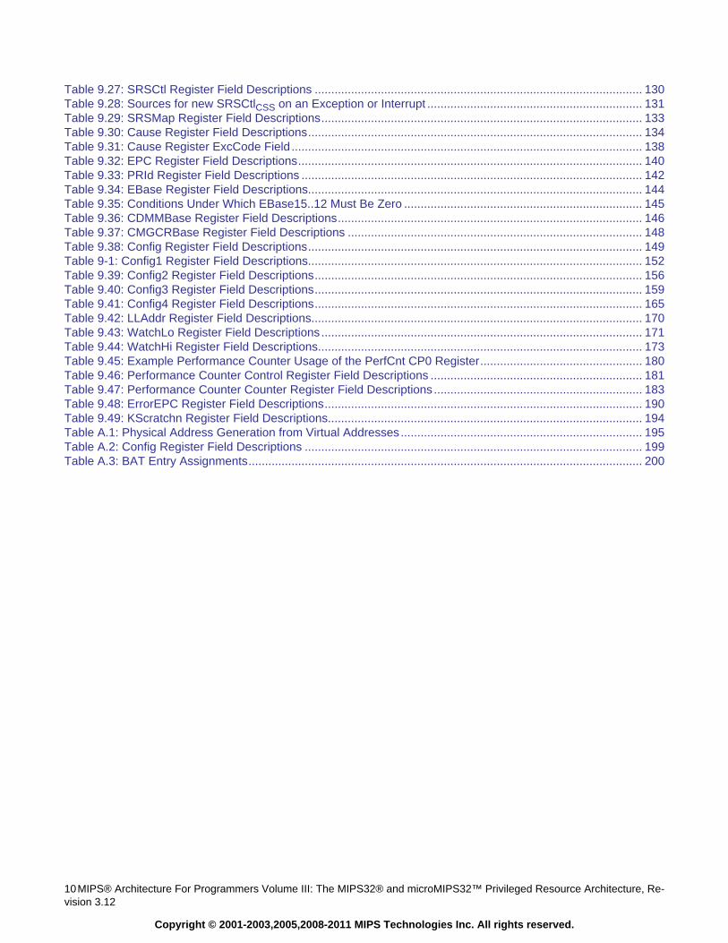
Table 9.27: SRSCtl Register Field Descriptions ................................................................................................... 130Table 9.28: Sources for new SRSCtlCSS on an Exception or Interrupt ................................................................. 131Table 9.29: SRSMap Register Field Descriptions................................................................................................. 133Table 9.30: Cause Register Field Descriptions..................................................................................................... 134Table 9.31: Cause Register ExcCode Field .......................................................................................................... 138Table 9.32: EPC Register Field Descriptions........................................................................................................ 140Table 9.33: PRId Register Field Descriptions ....................................................................................................... 142Table 9.34: EBase Register Field Descriptions..................................................................................................... 144Table 9.35: Conditions Under Which EBase15..12 Must Be Zero ........................................................................ 145Table 9.36: CDMMBase Register Field Descriptions............................................................................................ 146Table 9.37: CMGCRBase Register Field Descriptions ......................................................................................... 148Table 9.38: Config Register Field Descriptions..................................................................................................... 149Table 9-1: Config1 Register Field Descriptions..................................................................................................... 152Table 9.39: Config2 Register Field Descriptions................................................................................................... 156Table 9.40: Config3 Register Field Descriptions................................................................................................... 159Table 9.41: Config4 Register Field Descriptions................................................................................................... 165Table 9.42: LLAddr Register Field Descriptions.................................................................................................... 170Table 9.43: WatchLo Register Field Descriptions................................................................................................. 171Table 9.44: WatchHi Register Field Descriptions.................................................................................................. 173Table 9.45: Example Performance Counter Usage of the PerfCnt CP0 Register................................................. 180Table 9.46: Performance Counter Control Register Field Descriptions ................................................................ 181Table 9.47: Performance Counter Counter Register Field Descriptions ............................................................... 183Table 9.48: ErrorEPC Register Field Descriptions................................................................................................ 190Table 9.49: KScratchn Register Field Descriptions............................................................................................... 194Table A.1: Physical Address Generation from Virtual Addresses......................................................................... 195Table A.2: Config Register Field Descriptions ...................................................................................................... 199Table A.3: BAT Entry Assignments....................................................................................................................... 200
Chapter 1
MIPS® Architecture For Programmers Volume III: The MIPS32® and microMIPS32™ Privileged Resource Architecture, Revi-sion 3.12 11
Copyright © 2001-2003,2005,2008-2011 MIPS Technologies Inc. All rights reserved.
About This Book
The MIPS® Architecture For Programmers Volume III: The MIPS32® and microMIPS32™ Privileged ResourceArchitecture comes as part of a multi-volume set.
• Volume I-A describes conventions used throughout the document set, and provides an introduction to theMIPS32® Architecture
• Volume I-B describes conventions used throughout the document set, and provides an introduction to themicroMIPS32™ Architecture
• Volume II-A provides detailed descriptions of each instruction in the MIPS32® instruction set
• Volume II-B provides detailed descriptions of each instruction in the microMIPS32™ instruction set
• Volume III describes the MIPS32® and microMIPS32™ Privileged Resource Architecture which defines andgoverns the behavior of the privileged resources included in a MIPS® processor implementation
• Volume IV-a describes the MIPS16e™ Application-Specific Extension to the MIPS32® Architecture. Beginningwith Release 3 of the Architecture, microMIPS is the preferred solution for smaller code size.
• Volume IV-b describes the MDMX™ Application-Specific Extension to the MIPS64® Architecture andmicroMIPS64™. It is not applicable to the MIPS32® document set nor the microMIPS32™ document set
• Volume IV-c describes the MIPS-3D® Application-Specific Extension to the MIPS® Architecture
• Volume IV-d describes the SmartMIPS®Application-Specific Extension to the MIPS32® Architecture and themicroMIPS32™ Architecture
• Volume IV-e describes the MIPS® DSP Application-Specific Extension to the MIPS® Architecture
• Volume IV-f describes the MIPS® MT Application-Specific Extension to the MIPS® Architecture
• Volume IV-h describes the MIPS® MCU Application-Specific Extension to the MIPS® Architecture
1.1 Typographical Conventions
This section describes the use of italic, bold and courier fonts in this book.
1.1.1 Italic Text
• is used for emphasis
About This Book
12MIPS® Architecture For Programmers Volume III: The MIPS32® and microMIPS32™ Privileged Resource Architecture, Re-vision 3.12
Copyright © 2001-2003,2005,2008-2011 MIPS Technologies Inc. All rights reserved.
• is used for bits, fields, registers, that are important from a software perspective (for instance, address bits used bysoftware, and programmable fields and registers), and various floating point instruction formats, such as S, D,and PS
• is used for the memory access types, such as cached and uncached
1.1.2 Bold Text
• represents a term that is being defined
• is used for bits and fields that are important from a hardware perspective (for instance, register bits, which arenot programmable but accessible only to hardware)
• is used for ranges of numbers; the range is indicated by an ellipsis. For instance, 5..1 indicates numbers 5 through1
• is used to emphasize UNPREDICTABLE and UNDEFINED behavior, as defined below.
1.1.3 Courier Text
Courier fixed-width font is used for text that is displayed on the screen, and for examples of code and instructionpseudocode.
1.2 UNPREDICTABLE and UNDEFINED
The terms UNPREDICTABLE and UNDEFINED are used throughout this book to describe the behavior of theprocessor in certain cases. UNDEFINED behavior or operations can occur only as the result of executing instructionsin a privileged mode (i.e., in Kernel Mode or Debug Mode, or with the CP0 usable bit set in the Status register).Unprivileged software can never cause UNDEFINED behavior or operations. Conversely, both privileged andunprivileged software can cause UNPREDICTABLE results or operations.
1.2.1 UNPREDICTABLE
UNPREDICTABLE results may vary from processor implementation to implementation, instruction to instruction,or as a function of time on the same implementation or instruction. Software can never depend on results that areUNPREDICTABLE. UNPREDICTABLE operations may cause a result to be generated or not. If a result is gener-ated, it is UNPREDICTABLE. UNPREDICTABLE operations may cause arbitrary exceptions.
UNPREDICTABLE results or operations have several implementation restrictions:
• Implementations of operations generating UNPREDICTABLE results must not depend on any data source(memory or internal state) which is inaccessible in the current processor mode
• UNPREDICTABLE operations must not read, write, or modify the contents of memory or internal state whichis inaccessible in the current processor mode. For example, UNPREDICTABLE operations executed in usermode must not access memory or internal state that is only accessible in Kernel Mode or Debug Mode or inanother process
• UNPREDICTABLE operations must not halt or hang the processor
1.3 Special Symbols in Pseudocode Notation
MIPS® Architecture For Programmers Volume III: The MIPS32® and microMIPS32™ Privileged Resource Architecture, Revi-sion 3.12 13
Copyright © 2001-2003,2005,2008-2011 MIPS Technologies Inc. All rights reserved.
1.2.2 UNDEFINED
UNDEFINED operations or behavior may vary from processor implementation to implementation, instruction toinstruction, or as a function of time on the same implementation or instruction. UNDEFINED operations or behaviormay vary from nothing to creating an environment in which execution can no longer continue. UNDEFINED opera-tions or behavior may cause data loss.
UNDEFINED operations or behavior has one implementation restriction:
• UNDEFINED operations or behavior must not cause the processor to hang (that is, enter a state from whichthere is no exit other than powering down the processor). The assertion of any of the reset signals must restorethe processor to an operational state
1.2.3 UNSTABLE
UNSTABLE results or values may vary as a function of time on the same implementation or instruction. UnlikeUNPREDICTABLE values, software may depend on the fact that a sampling of an UNSTABLE value results in alegal transient value that was correct at some point in time prior to the sampling.
UNSTABLE values have one implementation restriction:
• Implementations of operations generating UNSTABLE results must not depend on any data source (memory orinternal state) which is inaccessible in the current processor mode
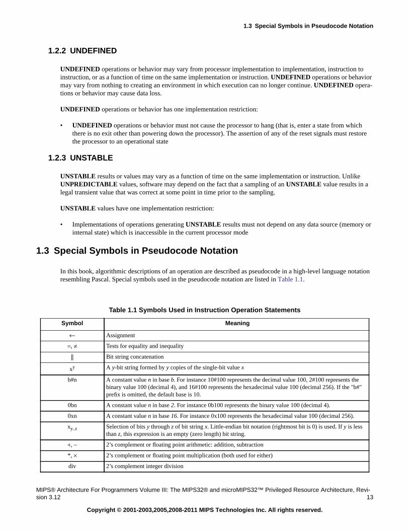
1.3 Special Symbols in Pseudocode Notation
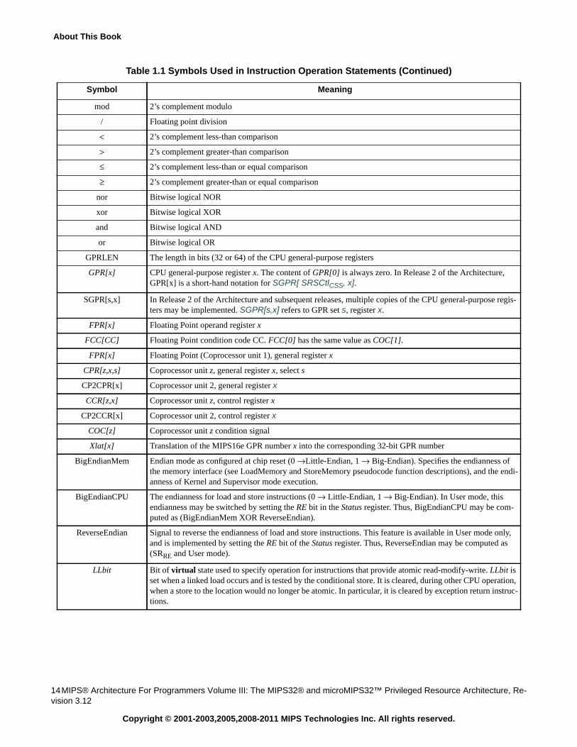
In this book, algorithmic descriptions of an operation are described as pseudocode in a high-level language notationresembling Pascal. Special symbols used in the pseudocode notation are listed in Table 1.1.
Table 1.1 Symbols Used in Instruction Operation Statements
Symbol Meaning
← Assignment
=, ≠ Tests for equality and inequality
|| Bit string concatenation
xy A y-bit string formed by y copies of the single-bit value x
b#n A constant value n in base b. For instance 10#100 represents the decimal value 100, 2#100 represents thebinary value 100 (decimal 4), and 16#100 represents the hexadecimal value 100 (decimal 256). If the "b#"prefix is omitted, the default base is 10.
0bn A constant value n in base 2. For instance 0b100 represents the binary value 100 (decimal 4).
0xn A constant value n in base 16. For instance 0x100 represents the hexadecimal value 100 (decimal 256).
xy..z Selection of bits y through z of bit string x. Little-endian bit notation (rightmost bit is 0) is used. If y is lessthan z, this expression is an empty (zero length) bit string.
+, − 2’s complement or floating point arithmetic: addition, subtraction
*, × 2’s complement or floating point multiplication (both used for either)
div 2’s complement integer division
About This Book
14MIPS® Architecture For Programmers Volume III: The MIPS32® and microMIPS32™ Privileged Resource Architecture, Re-vision 3.12
Copyright © 2001-2003,2005,2008-2011 MIPS Technologies Inc. All rights reserved.
mod 2’s complement modulo
/ Floating point division
< 2’s complement less-than comparison
> 2’s complement greater-than comparison
≤ 2’s complement less-than or equal comparison
≥ 2’s complement greater-than or equal comparison
nor Bitwise logical NOR
xor Bitwise logical XOR
and Bitwise logical AND
or Bitwise logical OR
GPRLEN The length in bits (32 or 64) of the CPU general-purpose registers
GPR[x] CPU general-purpose register x. The content of GPR[0] is always zero. In Release 2 of the Architecture,GPR[x] is a short-hand notation for SGPR[ SRSCtlCSS, x].
SGPR[s,x] In Release 2 of the Architecture and subsequent releases, multiple copies of the CPU general-purpose regis-ters may be implemented. SGPR[s,x] refers to GPR set s, register x.
FPR[x] Floating Point operand register x
FCC[CC] Floating Point condition code CC. FCC[0] has the same value as COC[1].
FPR[x] Floating Point (Coprocessor unit 1), general register x
CPR[z,x,s] Coprocessor unit z, general register x, select s
CP2CPR[x] Coprocessor unit 2, general register x
CCR[z,x] Coprocessor unit z, control register x
CP2CCR[x] Coprocessor unit 2, control register x
COC[z] Coprocessor unit z condition signal
Xlat[x] Translation of the MIPS16e GPR number x into the corresponding 32-bit GPR number
BigEndianMem Endian mode as configured at chip reset (0 →Little-Endian, 1 → Big-Endian). Specifies the endianness ofthe memory interface (see LoadMemory and StoreMemory pseudocode function descriptions), and the endi-anness of Kernel and Supervisor mode execution.
BigEndianCPU The endianness for load and store instructions (0 → Little-Endian, 1 → Big-Endian). In User mode, thisendianness may be switched by setting the RE bit in the Status register. Thus, BigEndianCPU may be com-puted as (BigEndianMem XOR ReverseEndian).
ReverseEndian Signal to reverse the endianness of load and store instructions. This feature is available in User mode only,and is implemented by setting the RE bit of the Status register. Thus, ReverseEndian may be computed as(SRRE and User mode).
LLbit Bit of virtual state used to specify operation for instructions that provide atomic read-modify-write. LLbit isset when a linked load occurs and is tested by the conditional store. It is cleared, during other CPU operation,when a store to the location would no longer be atomic. In particular, it is cleared by exception return instruc-tions.
Table 1.1 Symbols Used in Instruction Operation Statements (Continued)
Symbol Meaning
1.3 Special Symbols in Pseudocode Notation
MIPS® Architecture For Programmers Volume III: The MIPS32® and microMIPS32™ Privileged Resource Architecture, Revi-sion 3.12 15
Copyright © 2001-2003,2005,2008-2011 MIPS Technologies Inc. All rights reserved.
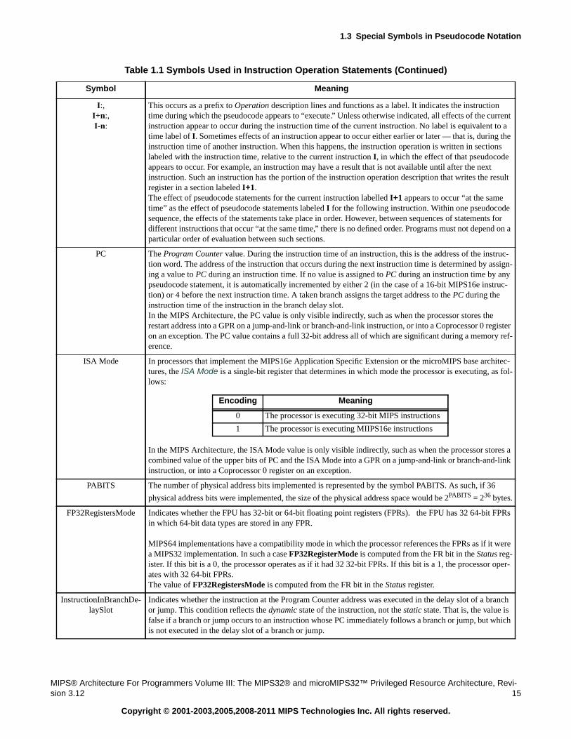
I:,I+n:,I-n:
This occurs as a prefix to Operation description lines and functions as a label. It indicates the instructiontime during which the pseudocode appears to “execute.” Unless otherwise indicated, all effects of the currentinstruction appear to occur during the instruction time of the current instruction. No label is equivalent to atime label of I. Sometimes effects of an instruction appear to occur either earlier or later — that is, during theinstruction time of another instruction. When this happens, the instruction operation is written in sectionslabeled with the instruction time, relative to the current instruction I, in which the effect of that pseudocodeappears to occur. For example, an instruction may have a result that is not available until after the nextinstruction. Such an instruction has the portion of the instruction operation description that writes the resultregister in a section labeled I+1.The effect of pseudocode statements for the current instruction labelled I+1 appears to occur “at the sametime” as the effect of pseudocode statements labeled I for the following instruction. Within one pseudocodesequence, the effects of the statements take place in order. However, between sequences of statements fordifferent instructions that occur “at the same time,” there is no defined order. Programs must not depend on aparticular order of evaluation between such sections.
PC The Program Counter value. During the instruction time of an instruction, this is the address of the instruc-tion word. The address of the instruction that occurs during the next instruction time is determined by assign-ing a value to PC during an instruction time. If no value is assigned to PC during an instruction time by anypseudocode statement, it is automatically incremented by either 2 (in the case of a 16-bit MIPS16e instruc-tion) or 4 before the next instruction time. A taken branch assigns the target address to the PC during theinstruction time of the instruction in the branch delay slot.In the MIPS Architecture, the PC value is only visible indirectly, such as when the processor stores therestart address into a GPR on a jump-and-link or branch-and-link instruction, or into a Coprocessor 0 registeron an exception. The PC value contains a full 32-bit address all of which are significant during a memory ref-erence.
ISA Mode In processors that implement the MIPS16e Application Specific Extension or the microMIPS base architec-tures, the ISA Mode is a single-bit register that determines in which mode the processor is executing, as fol-lows:
In the MIPS Architecture, the ISA Mode value is only visible indirectly, such as when the processor stores acombined value of the upper bits of PC and the ISA Mode into a GPR on a jump-and-link or branch-and-linkinstruction, or into a Coprocessor 0 register on an exception.
PABITS The number of physical address bits implemented is represented by the symbol PABITS. As such, if 36
physical address bits were implemented, the size of the physical address space would be 2PABITS = 236 bytes.
FP32RegistersMode Indicates whether the FPU has 32-bit or 64-bit floating point registers (FPRs). the FPU has 32 64-bit FPRsin which 64-bit data types are stored in any FPR.
MIPS64 implementations have a compatibility mode in which the processor references the FPRs as if it werea MIPS32 implementation. In such a case FP32RegisterMode is computed from the FR bit in the Status reg-ister. If this bit is a 0, the processor operates as if it had 32 32-bit FPRs. If this bit is a 1, the processor oper-ates with 32 64-bit FPRs.The value of FP32RegistersMode is computed from the FR bit in the Status register.
InstructionInBranchDe-laySlot
Indicates whether the instruction at the Program Counter address was executed in the delay slot of a branchor jump. This condition reflects the dynamic state of the instruction, not the static state. That is, the value isfalse if a branch or jump occurs to an instruction whose PC immediately follows a branch or jump, but whichis not executed in the delay slot of a branch or jump.
Table 1.1 Symbols Used in Instruction Operation Statements (Continued)
Symbol Meaning
Encoding Meaning
0 The processor is executing 32-bit MIPS instructions
1 The processor is executing MIIPS16e instructions
About This Book
16MIPS® Architecture For Programmers Volume III: The MIPS32® and microMIPS32™ Privileged Resource Architecture, Re-vision 3.12
Copyright © 2001-2003,2005,2008-2011 MIPS Technologies Inc. All rights reserved.
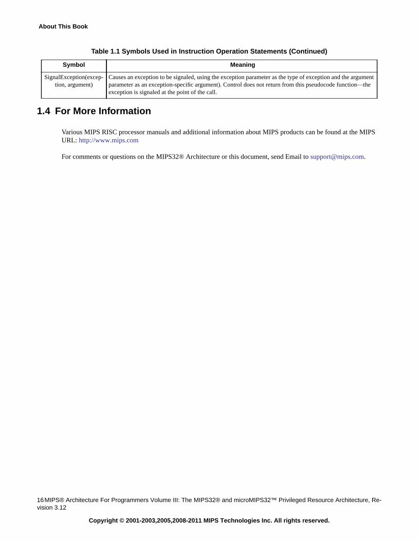
1.4 For More Information
Various MIPS RISC processor manuals and additional information about MIPS products can be found at the MIPSURL: http://www.mips.com
For comments or questions on the MIPS32® Architecture or this document, send Email to [email protected].
SignalException(excep-tion, argument)
Causes an exception to be signaled, using the exception parameter as the type of exception and the argumentparameter as an exception-specific argument). Control does not return from this pseudocode function—theexception is signaled at the point of the call.
Table 1.1 Symbols Used in Instruction Operation Statements (Continued)
Symbol Meaning
Chapter 2
MIPS® Architecture For Programmers Volume III: The MIPS32® and microMIPS32™ Privileged Resource Architecture, Revi-sion 3.12 17
Copyright © 2001-2003,2005,2008-2011 MIPS Technologies Inc. All rights reserved.
The MIPS32 and microMIPS32 Privileged ResourceArchitecture
2.1 Introduction
The MIPS32 and microMIPS32 Privileged Resource Architecture (PRA) is a set of environments and capabilities onwhich the Instruction Set Architectures operate. The effects of some components of the PRA are user-visible, forinstance, the virtual memory layout. Many other components are visible only to the operating system kernel and tosystems programmers. The PRA provides the mechanisms necessary to manage the resources of the CPU: virtualmemory, caches, exceptions and user contexts. This chapter describes these mechanisms.
2.2 The MIPS Coprocessor Model
The MIPS ISA provides for up to 4 coprocessors. A coprocessor extends the functionality of the MIPS ISA, whilesharing the instruction fetch and execution control logic of the CPU. Some coprocessors, such as the system copro-cessor and the floating point unit are standard parts of the ISA, and are specified as such in the architecture docu-ments. Coprocessors are generally optional, with one exception: CP0, the system coprocessor, is required. CP0 is theISA interface to the Privileged Resource Architecture and provides full control of the processor state and modes.
2.2.1 CP0 - The System Coprocessor
CP0 provides an abstraction of the functions necessary to support an operating system: exception handling, memorymanagement, scheduling, and control of critical resources. The interface to CP0 is through various instructionsencoded with the COP0 opcode, including the ability to move data to and from the CP0 registers, and specific func-tions that modify CP0 state. The CP0 registers and the interaction with them make up much of the PrivilegedResource Architecture.
2.2.2 CP0 Registers
The CP0 registers provide the interface between the ISA and the PRA. The CP0 registers are described in Chapter 9.

The MIPS32 and microMIPS32 Privileged Resource Architecture
18MIPS® Architecture For Programmers Volume III: The MIPS32® and microMIPS32™ Privileged Resource Architecture, Re-vision 3.12
Copyright © 2001-2003,2005,2008-2011 MIPS Technologies Inc. All rights reserved.
Chapter 3
MIPS® Architecture For Programmers Volume III: The MIPS32® and microMIPS32™ Privileged Resource Architecture, Revi-sion 3.12 19
Copyright © 2001-2003,2005,2008-2011 MIPS Technologies Inc. All rights reserved.
MIPS32 and microMIPS32 Operating Modes
The MIPS32 and microMIPS32 PRA requires two operating mode: User Mode and Kernel Mode. When operating inUser Mode, the programmer has access to the CPU and FPU registers that are provided by the ISA and to a flat, uni-form virtual memory address space. When operating in Kernel Mode, the system programmer has access to the fullcapabilities of the processor, including the ability to change virtual memory mapping, control the system environ-ment, and context switch between processes.
In addition, the MIPS PRA supports the implementation of two additional modes: Supervisor Mode and EJTAGDebug Mode. Refer to the EJTAG specification for a description of Debug Mode.
In Release 2 of the MIPS32 Architecture, support was added for 64-bit coprocessors (and, in particular, 64-bit float-ing point units) with 32-bit CPUs. As such, certain floating point instructions which were previously enabled by64-bit operations on a MIPS64 processor are now enabled by a new 64-bit floating point operations enabled. Release3 (e.g. MIPSr3) introduced the microMIPS instruction set, so all microMIPS processors may implement a 64-bitfloating point unit.
3.1 Debug Mode
For processors that implement EJTAG, the processor is operating in Debug Mode if the DM bit in the CP0 Debugregister is a one. If the processor is running in Debug Mode, it has full access to all resources that are available to Ker-nel Mode operation.
3.2 Kernel Mode
The processor is operating in Kernel Mode when the DM bit in the Debug register is a zero (if the processor imple-ments Debug Mode), and any of the following three conditions is true:
• The KSU field in the CP0 Status register contains 0b00
• The EXL bit in the Status register is one
• The ERL bit in the Status register is one
The processor enters Kernel Mode at power-up, or as the result of an interrupt, exception, or error. The processorleaves Kernel Mode and enters User Mode or Supervisor Mode when all of the previous three conditions are false,usually as the result of an ERET instruction.
3.3 Supervisor Mode
The processor is operating in Supervisor Mode (if that optional mode is implemented by the processor) when all ofthe following conditions are true:
MIPS32 and microMIPS32 Operating Modes
20MIPS® Architecture For Programmers Volume III: The MIPS32® and microMIPS32™ Privileged Resource Architecture, Re-vision 3.12
Copyright © 2001-2003,2005,2008-2011 MIPS Technologies Inc. All rights reserved.
• The DM bit in the Debug register is a zero (if the processor implements Debug Mode)
• The KSU field in the Status register contains 0b01
• The EXL and ERL bits in the Status register are both zero
3.4 User Mode
The processor is operating in User Mode when all of the following conditions are true:
• The DM bit in the Debug register is a zero (if the processor implements Debug Mode)
• The KSU field in the Status register contains 0b10
• The EXL and ERL bits in the Status register are both zero
3.5 Other Modes
3.5.1 64-bit Floating Point Operations Enable
Instructions that are implemented by a 64-bit floating point unit are legal under any of the following conditions:
• In an implementation of Release 1 of the Architecture, 64-bit floating point operations are never enabled in aMIPS32 processor.
• In an implementation of Release 2 (and subsequent releases) of the Architecture, 64-bit floating point operationsare enabled if the F64 bit in the FIR register is a one. The processor must also implement the floating point datatype. Release 3 (e.g. MIPSr3) introduced the microMIPS instruction set. So on all microMIPS processors, 64-bitfloating point operations are enabled if the F64 bit in the FIR register is a one .
3.5.2 64-bit FPR Enable
Access to 64-bit FPRs is controlled by the FR bit in the Status register. If the FR bit is one, the FPRs are interpreted as32 64-bit registers that may contain any data type. If the FR bit is zero, the FPRs are interpreted as 32 32-bit registers,any of which may contain a 32-bit data type (W, S). In this case, 64-bit data types are contained in even-odd pairs ofregisters.
64-bit FPRs are supported in a MIPS64 processor in Release 1 of the Architecture, or in a 64-bit floating point unit,for both MIPS32 and MIPS64 processors, in Release 2 of the Architecture. 64-bit FPRs are supported for all proces-sors using Architecture releases subsequent to Release 2, including all microMIPS processors.
The operation of the processor is UNPREDICTABLE under the following conditions:
• The FR bit is a zero, 64-bit operations are enabled, and a floating point instruction is executed whose datatype isL or PS.
• The FR bit is a zero and an odd register is referenced by an instruction whose datatype is 64-bits
3.5 Other Modes
MIPS® Architecture For Programmers Volume III: The MIPS32® and microMIPS32™ Privileged Resource Architecture, Revi-sion 3.12 21
Copyright © 2001-2003,2005,2008-2011 MIPS Technologies Inc. All rights reserved.
3.5.3 Coprocessor 0 Enable
Access to Coprocessor 0 registers are enabled under any of the following conditions:
• The processor is running in Kernel Mode or Debug Mode, as defined above
• The CU0 bit in the Status register is one.
3.5.4 ISA Mode
Release 3 of the Architecture (e.g. MIPSr3TM) introduced a second branch of the instruction set family,microMIPS32. Devices can implement both ISA branches (MIPS32 and microMIPS32) or only one branch.
The ISA Mode bit is used to denote which ISA branch to use when decoding instructions. This bit is normally not vis-ible to software. It’s value is saved to any GPR that would be used as a jump target address, such as GPR31 whenwritten by a JAL instruction or the source register for a JR instruction.
For processors that implement the MIPS32 ISA, the ISA Mode bit value of zero selects MIPS32. For processors thatimplement the microMIPS32 ISA, the ISA Mode bit value of one selects microMIPS32. For processors that imple-
ment the MIPS16eTM ASE, the ISA Mode bit value of one selects MIPS16e. A processor is not allowed to implementboth MIPS16e and microMIPS.
Please read Volume II-B: Introduction to the microMIPS32 Instruction Set, Section 5.3, “ISA Mode Switch” for amore in-depth description of ISA mode switching between the ISA branches and the ISA Mode bit.

MIPS32 and microMIPS32 Operating Modes
22MIPS® Architecture For Programmers Volume III: The MIPS32® and microMIPS32™ Privileged Resource Architecture, Re-vision 3.12
Copyright © 2001-2003,2005,2008-2011 MIPS Technologies Inc. All rights reserved.
Chapter 4
MIPS® Architecture For Programmers Volume III: The MIPS32® and microMIPS32™ Privileged Resource Architecture, Revi-sion 3.12 23
Copyright © 2001-2003,2005,2008-2011 MIPS Technologies Inc. All rights reserved.
Virtual Memory
4.1 Differences between Releases of the Architecture
4.1.1 Virtual Memory
In Release 1 of the Architecture, the minimum page size was 4KB, with optional support for pages as large as256MB. In Release 2 of the Architecture (and subsequent releases), optional support for 1KB pages was added foruse in specific embedded applications that require access to pages smaller than 4KB. Such usage is expected to be inconjunction with a default page size of 4KB and is not intended or suggested to replace the default 4KB page size but,rather, to augment it.
Support for 1KB pages involves the following changes:
• Addition of the PageGrain register. This register is also used by the SmartMIPS™ ASE specification, but bitsused by Release 2 of the Architecture and the SmartMIPS ASE specification do not overlap.
• Modification of the EntryHi register to enable writes to, and use of, bits 12..11 (VPN2X).
• Modification of the PageMask register to enable writes to, and use of, bits 12..11 (MaskX).
• Modification of the EntryLo0 and EntryLo1 registers to shift the PFN field to the left by 2 bits, when 1KB pagesupport is enabled, to create space for two lower-order physical address bits.
Support for 1KB pages is denoted by the Config3SP bit and enabled by the PageGrainESP bit.
4.1.2 Protection of Virtual Memory Pages
In Release 3 of the Architecture, e.g. MIPSr3, two optional control bits are added to each TLB entry. These bits, RI(Read Inhibit) and XI (Execute Inhibit), allows more types of protection to be used for virtual pages - includingwrite-only pages, non-executable pages.
This feature originated in the SmartMIPS ASE but has been modified from the original SmartMIPS definition. For theRelease 3 version of this feature, each of the RI and XI bits can be separately implemented. For the Release 3 versionof this feature, new exception codes are used when a TLB access does not obey the RI/XI bits.
4.1.3 Context Register
In Release 3 of the Architecture, e.g. MIPSr3, the Context register is a read/write register containing a address pointerthat can point to an arbitrary power-of-two aligned data structure in memory, such as an entry in the page table entry(PTE) array. In Releases 1 & 2, this pointer was defined to reference a fixed-sized 16-byte structure in memory withina linear array containing an entry for each even/odd virtual page pair. The Release 3 version of the Context registercan be used far more generally.
Virtual Memory
24MIPS® Architecture For Programmers Volume III: The MIPS32® and microMIPS32™ Privileged Resource Architecture, Re-vision 3.12
Copyright © 2001-2003,2005,2008-2011 MIPS Technologies Inc. All rights reserved.
This feature originated in the SmartMIPS ASE. This feature is optional in the Release 3 version of the base architec-ture.
4.2 Terminology
4.2.1 Address Space
An Address Space is the range of all possible addresses that can be generated. There is one 32-bit Address Space inthe MIPS32 Architecture.
4.2.2 Segment and Segment Size
A Segment is a defined subset of an Address Space that has self-consistent reference and access behavior. Segments
are either 229 or 231 bytes in size, depending on the specific Segment.
4.2.3 Physical Address Size (PABITS)
The number of physical address bits implemented is represented by the symbol PABITS. As such, if 36 physical
address bits were implemented, the size of the physical address space would be 2PABITS = 236 bytes. The format of the
EntryLo0 and EntryLo1 registers implicitly limits the physical address size to 236 bytes. Software may determine thevalue of PABITS by writing all ones to the EntryLo0 or EntryLo1 registers and reading the value back. Bits read as“1” from the PFN field allow software to determine the boundary between the PFN and 0 fields to calculate the valueof PABITS.
4.3 Virtual Address Spaces
MIPS® Architecture For Programmers Volume III: The MIPS32® and microMIPS32™ Privileged Resource Architecture, Revi-sion 3.12 25
Copyright © 2001-2003,2005,2008-2011 MIPS Technologies Inc. All rights reserved.
4.3 Virtual Address Spaces
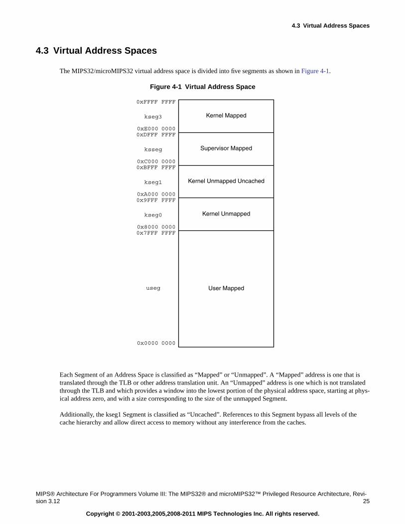
The MIPS32/microMIPS32 virtual address space is divided into five segments as shown in Figure 4-1.
Figure 4-1 Virtual Address Space
Each Segment of an Address Space is classified as “Mapped” or “Unmapped”. A “Mapped” address is one that istranslated through the TLB or other address translation unit. An “Unmapped” address is one which is not translatedthrough the TLB and which provides a window into the lowest portion of the physical address space, starting at phys-ical address zero, and with a size corresponding to the size of the unmapped Segment.
Additionally, the kseg1 Segment is classified as “Uncached”. References to this Segment bypass all levels of thecache hierarchy and allow direct access to memory without any interference from the caches.
0x0000 0000
useg
0x7FFF FFFF
User Mapped
Kernel Unmapped
0x8000 0000
kseg0
0x9FFF FFFF
Kernel Unmapped Uncached
0xA000 0000
kseg1
0xBFFF FFFF
Supervisor Mapped
0xC000 0000
ksseg
0xDFFF FFFF
Kernel Mapped
0xE000 0000
kseg3
0xFFFF FFFF
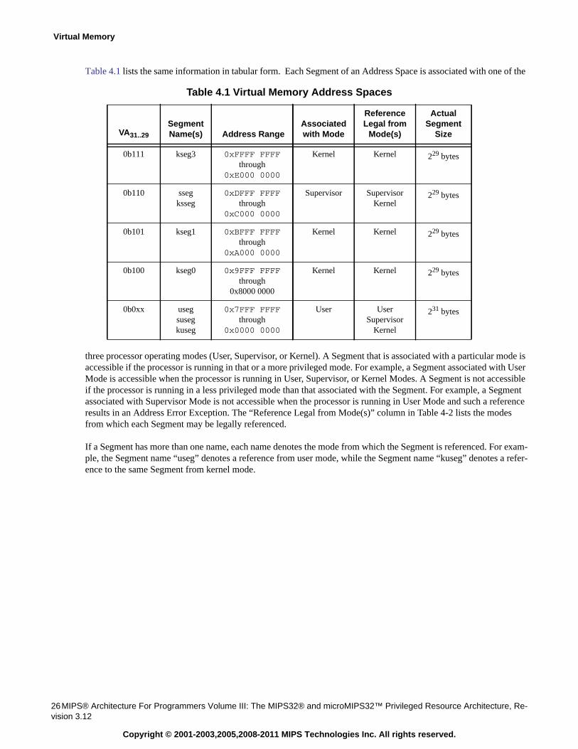
Virtual Memory
26MIPS® Architecture For Programmers Volume III: The MIPS32® and microMIPS32™ Privileged Resource Architecture, Re-vision 3.12
Copyright © 2001-2003,2005,2008-2011 MIPS Technologies Inc. All rights reserved.
Table 4.1 lists the same information in tabular form. Each Segment of an Address Space is associated with one of the
three processor operating modes (User, Supervisor, or Kernel). A Segment that is associated with a particular mode isaccessible if the processor is running in that or a more privileged mode. For example, a Segment associated with UserMode is accessible when the processor is running in User, Supervisor, or Kernel Modes. A Segment is not accessibleif the processor is running in a less privileged mode than that associated with the Segment. For example, a Segmentassociated with Supervisor Mode is not accessible when the processor is running in User Mode and such a referenceresults in an Address Error Exception. The “Reference Legal from Mode(s)” column in Table 4-2 lists the modesfrom which each Segment may be legally referenced.
If a Segment has more than one name, each name denotes the mode from which the Segment is referenced. For exam-ple, the Segment name “useg” denotes a reference from user mode, while the Segment name “kuseg” denotes a refer-ence to the same Segment from kernel mode.
Table 4.1 Virtual Memory Address Spaces
VA31..29
SegmentName(s) Address Range
Associatedwith Mode
ReferenceLegal from
Mode(s)
ActualSegment
Size
0b111 kseg3 0xFFFF FFFFthrough
0xE000 0000
Kernel Kernel 229 bytes
0b110 ssegksseg
0xDFFF FFFFthrough
0xC000 0000
Supervisor SupervisorKernel
229 bytes
0b101 kseg1 0xBFFF FFFFthrough
0xA000 0000
Kernel Kernel 229 bytes
0b100 kseg0 0x9FFF FFFFthrough
0x8000 0000
Kernel Kernel 229 bytes
0b0xx usegsusegkuseg
0x7FFF FFFFthrough
0x0000 0000
User UserSupervisor
Kernel
231 bytes
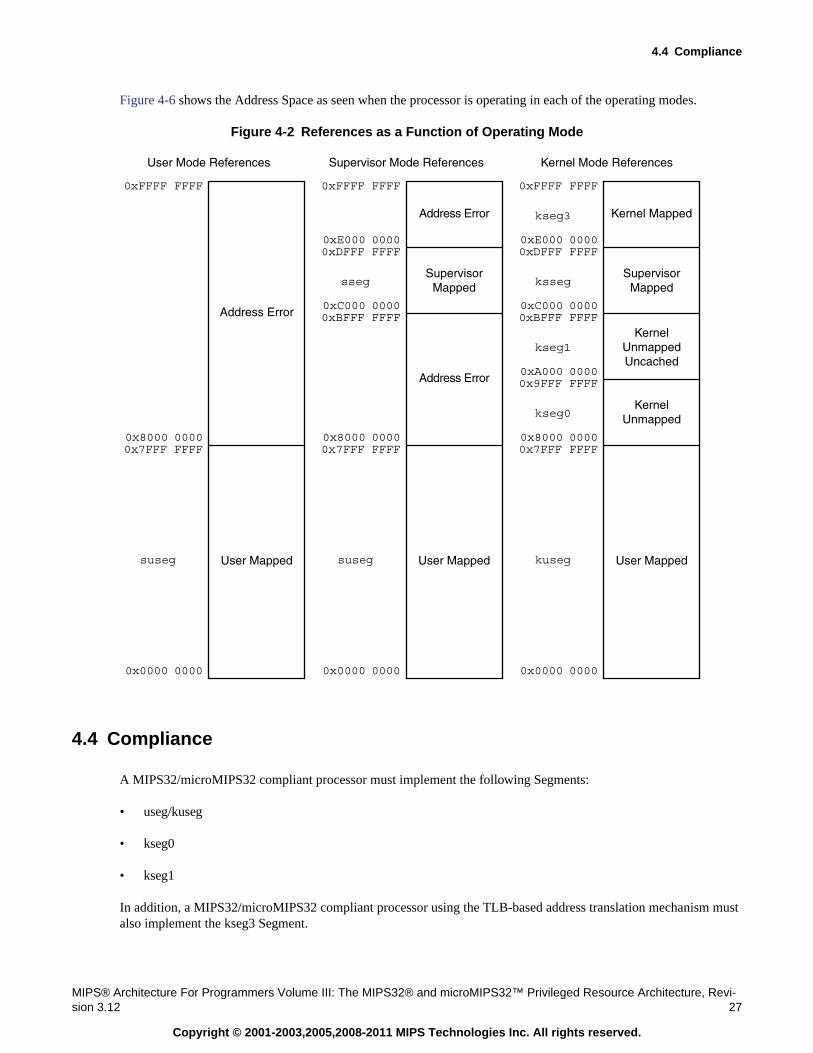
4.4 Compliance
MIPS® Architecture For Programmers Volume III: The MIPS32® and microMIPS32™ Privileged Resource Architecture, Revi-sion 3.12 27
Copyright © 2001-2003,2005,2008-2011 MIPS Technologies Inc. All rights reserved.
Figure 4-6 shows the Address Space as seen when the processor is operating in each of the operating modes.
Figure 4-2 References as a Function of Operating Mode
4.4 Compliance
A MIPS32/microMIPS32 compliant processor must implement the following Segments:
• useg/kuseg
• kseg0
• kseg1
In addition, a MIPS32/microMIPS32 compliant processor using the TLB-based address translation mechanism mustalso implement the kseg3 Segment.
User Mapped
0x0000 0000
kuseg
0x7FFF FFFF
Kernel Unmapped
0x8000 0000
kseg0
0x9FFF FFFF
Kernel Unmapped Uncached
0xA000 0000
kseg1
0xBFFF FFFF
Supervisor Mapped
0xC000 0000
ksseg
0xDFFF FFFF
Kernel Mapped
0xE000 0000
kseg3
0xFFFF FFFF
Kernel Mode References
User Mapped
0x0000 0000
suseg
0x7FFF FFFF
Address Error
0x8000 0000
0xBFFF FFFF
Supervisor Mapped
0xC000 0000
sseg
0xDFFF FFFF
Address Error
0xE000 0000
0xFFFF FFFF
Supervisor Mode References
User Mapped
0x0000 0000
suseg
0x7FFF FFFF
Address Error
0x8000 0000
0xFFFF FFFF
User Mode References
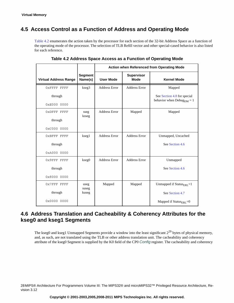
Virtual Memory
28MIPS® Architecture For Programmers Volume III: The MIPS32® and microMIPS32™ Privileged Resource Architecture, Re-vision 3.12
Copyright © 2001-2003,2005,2008-2011 MIPS Technologies Inc. All rights reserved.
4.5 Access Control as a Function of Address and Operating Mode
Table 4.2 enumerates the action taken by the processor for each section of the 32-bit Address Space as a function ofthe operating mode of the processor. The selection of TLB Refill vector and other special-cased behavior is also listedfor each reference.
4.6 Address Translation and Cacheability & Coherency Attributes for thekseg0 and kseg1 Segments
The kseg0 and kseg1 Unmapped Segments provide a window into the least significant 229 bytes of physical memory,and, as such, are not translated using the TLB or other address translation unit. The cacheability and coherencyattribute of the kseg0 Segment is supplied by the K0 field of the CP0 Config register. The cacheability and coherency
Table 4.2 Address Space Access as a Function of Operating Mode
Virtual Address RangeSegmentName(s)
Action when Referenced from Operating Mode
User ModeSupervisor
Mode Kernel Mode
0xFFFF FFFF
through
0xE000 0000
kseg3 Address Error Address Error Mapped
See Section 4.8 for specialbehavior when DebugDM = 1
0xDFFF FFFF
through
0xC000 0000
ssegksseg
Address Error Mapped Mapped
0xBFFF FFFF
through
0xA000 0000
kseg1 Address Error Address Error Unmapped, Uncached
See Section 4.6
0x9FFF FFFF
through
0x8000 0000
kseg0 Address Error Address Error Unmapped
See Section 4.6
0x7FFF FFFF
through
0x0000 0000
usegsusegkuseg
Mapped Mapped Unmapped if StatusERL=1
See Section 4.7
Mapped if StatusERL=0
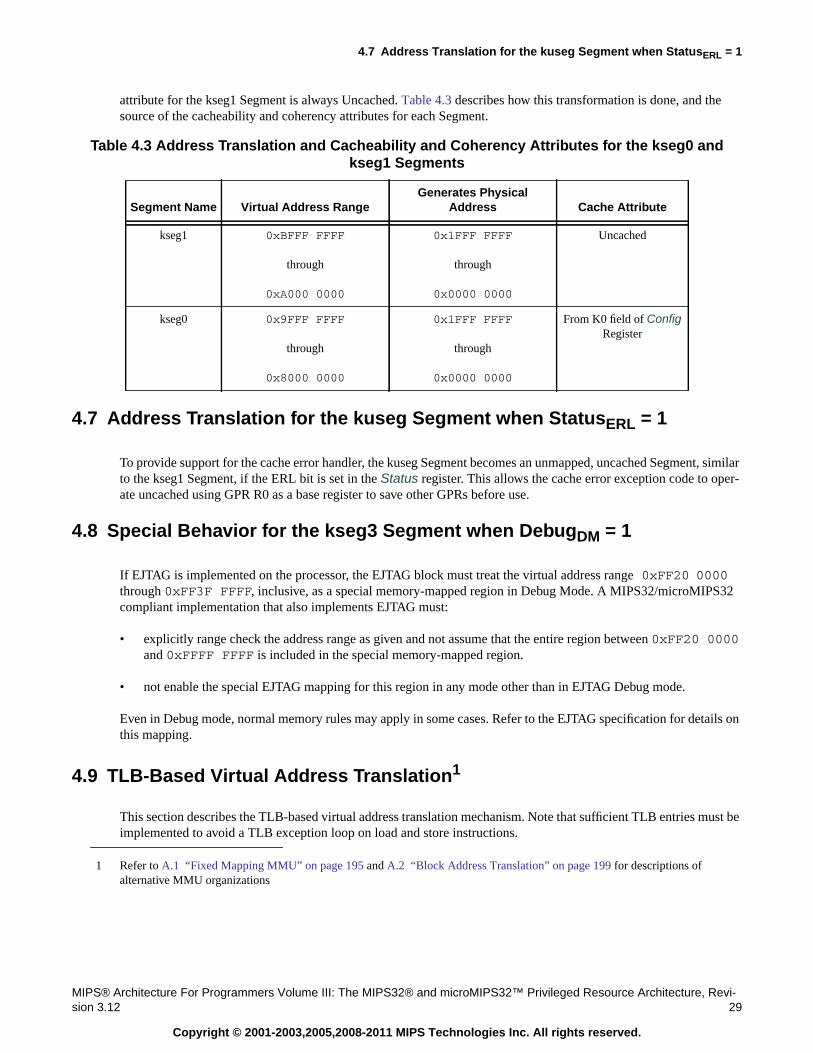
4.7 Address Translation for the kuseg Segment when StatusERL = 1
MIPS® Architecture For Programmers Volume III: The MIPS32® and microMIPS32™ Privileged Resource Architecture, Revi-sion 3.12 29
Copyright © 2001-2003,2005,2008-2011 MIPS Technologies Inc. All rights reserved.
attribute for the kseg1 Segment is always Uncached. Table 4.3 describes how this transformation is done, and thesource of the cacheability and coherency attributes for each Segment.
4.7 Address Translation for the kuseg Segment when StatusERL = 1
To provide support for the cache error handler, the kuseg Segment becomes an unmapped, uncached Segment, similarto the kseg1 Segment, if the ERL bit is set in the Status register. This allows the cache error exception code to oper-ate uncached using GPR R0 as a base register to save other GPRs before use.
4.8 Special Behavior for the kseg3 Segment when DebugDM = 1
If EJTAG is implemented on the processor, the EJTAG block must treat the virtual address range 0xFF20 0000through 0xFF3F FFFF, inclusive, as a special memory-mapped region in Debug Mode. A MIPS32/microMIPS32compliant implementation that also implements EJTAG must:
• explicitly range check the address range as given and not assume that the entire region between 0xFF20 0000and 0xFFFF FFFF is included in the special memory-mapped region.
• not enable the special EJTAG mapping for this region in any mode other than in EJTAG Debug mode.
Even in Debug mode, normal memory rules may apply in some cases. Refer to the EJTAG specification for details onthis mapping.
4.9 TLB-Based Virtual Address Translation1
This section describes the TLB-based virtual address translation mechanism. Note that sufficient TLB entries must beimplemented to avoid a TLB exception loop on load and store instructions.
Table 4.3 Address Translation and Cacheability and Coherency Attributes for the kseg0 andkseg1 Segments
Segment Name Virtual Address RangeGenerates Physical
Address Cache Attribute
kseg1 0xBFFF FFFF
through
0xA000 0000
0x1FFF FFFF
through
0x0000 0000
Uncached
kseg0 0x9FFF FFFF
through
0x8000 0000
0x1FFF FFFF
through
0x0000 0000
From K0 field of ConfigRegister
1 Refer to A.1 “Fixed Mapping MMU” on page 195 and A.2 “Block Address Translation” on page 199 for descriptions ofalternative MMU organizations
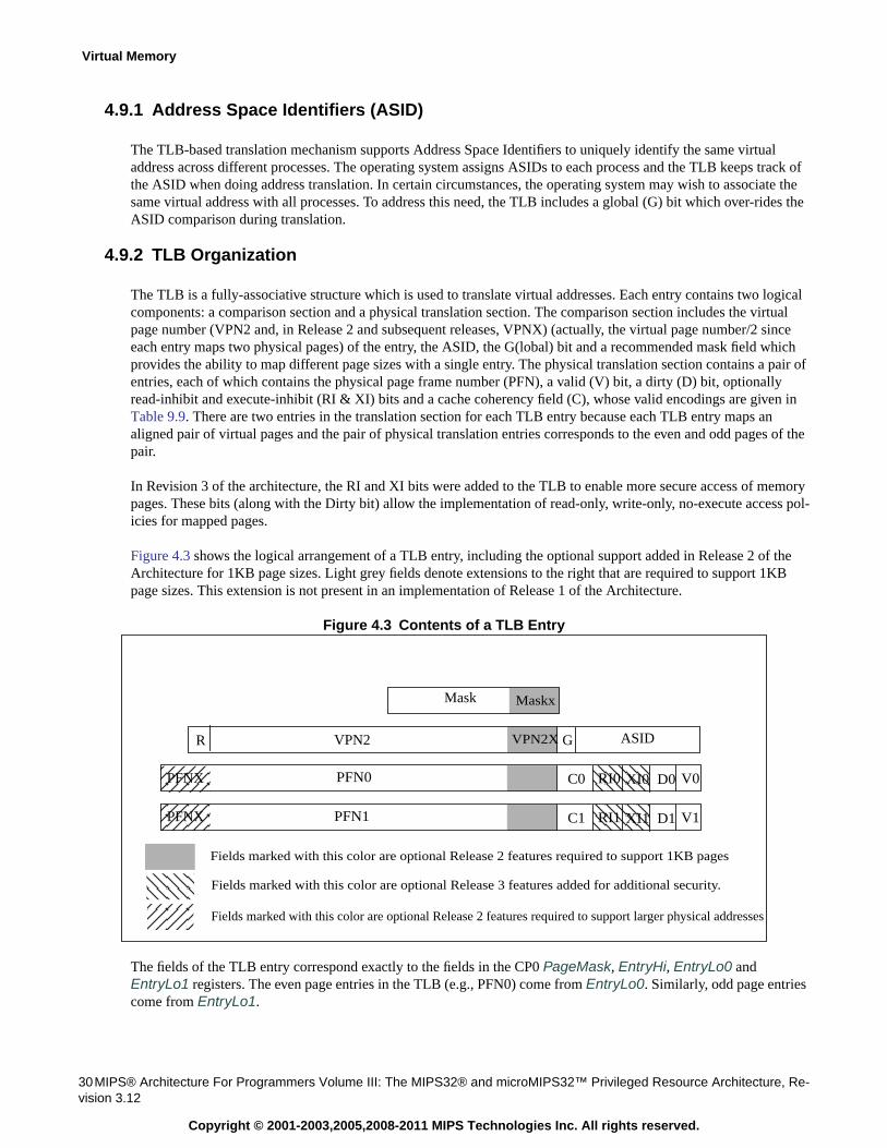
Virtual Memory
30MIPS® Architecture For Programmers Volume III: The MIPS32® and microMIPS32™ Privileged Resource Architecture, Re-vision 3.12
Copyright © 2001-2003,2005,2008-2011 MIPS Technologies Inc. All rights reserved.
4.9.1 Address Space Identifiers (ASID)
The TLB-based translation mechanism supports Address Space Identifiers to uniquely identify the same virtualaddress across different processes. The operating system assigns ASIDs to each process and the TLB keeps track ofthe ASID when doing address translation. In certain circumstances, the operating system may wish to associate thesame virtual address with all processes. To address this need, the TLB includes a global (G) bit which over-rides theASID comparison during translation.
4.9.2 TLB Organization
The TLB is a fully-associative structure which is used to translate virtual addresses. Each entry contains two logicalcomponents: a comparison section and a physical translation section. The comparison section includes the virtualpage number (VPN2 and, in Release 2 and subsequent releases, VPNX) (actually, the virtual page number/2 sinceeach entry maps two physical pages) of the entry, the ASID, the G(lobal) bit and a recommended mask field whichprovides the ability to map different page sizes with a single entry. The physical translation section contains a pair ofentries, each of which contains the physical page frame number (PFN), a valid (V) bit, a dirty (D) bit, optionallyread-inhibit and execute-inhibit (RI & XI) bits and a cache coherency field (C), whose valid encodings are given inTable 9.9. There are two entries in the translation section for each TLB entry because each TLB entry maps analigned pair of virtual pages and the pair of physical translation entries corresponds to the even and odd pages of thepair.
In Revision 3 of the architecture, the RI and XI bits were added to the TLB to enable more secure access of memorypages. These bits (along with the Dirty bit) allow the implementation of read-only, write-only, no-execute access pol-icies for mapped pages.
Figure 4.3 shows the logical arrangement of a TLB entry, including the optional support added in Release 2 of theArchitecture for 1KB page sizes. Light grey fields denote extensions to the right that are required to support 1KBpage sizes. This extension is not present in an implementation of Release 1 of the Architecture.
Figure 4.3 Contents of a TLB Entry
The fields of the TLB entry correspond exactly to the fields in the CP0 PageMask, EntryHi, EntryLo0 andEntryLo1 registers. The even page entries in the TLB (e.g., PFN0) come from EntryLo0. Similarly, odd page entriescome from EntryLo1.
PFNX
G ASIDVPN2
Mask
PFN1 D1 V1RI1 XI1C1
Maskx
VPN2X
PFN0 D0 V0RI0 XI0C0
Fields marked with this color are optional Release 2 features required to support 1KB pages
Fields marked with this color are optional Release 3 features added for additional security.
PFNX
R
Fields marked with this color are optional Release 2 features required to support larger physical addresses
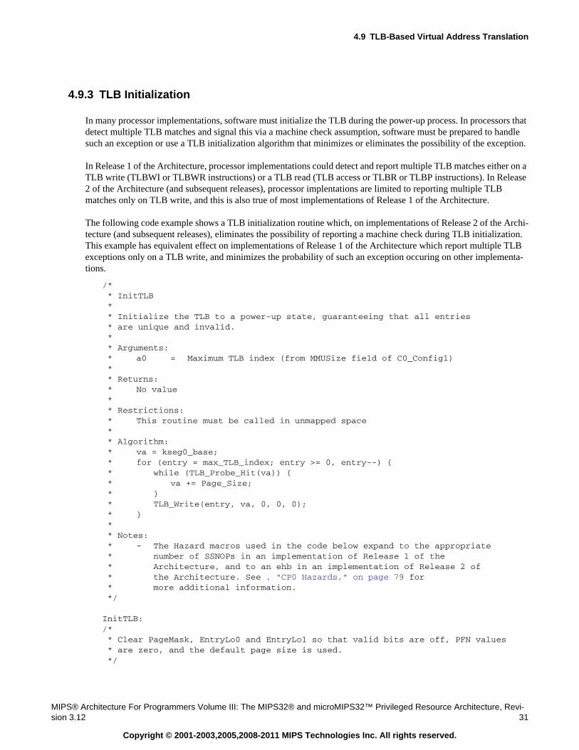
4.9 TLB-Based Virtual Address Translation
MIPS® Architecture For Programmers Volume III: The MIPS32® and microMIPS32™ Privileged Resource Architecture, Revi-sion 3.12 31
Copyright © 2001-2003,2005,2008-2011 MIPS Technologies Inc. All rights reserved.
4.9.3 TLB Initialization
In many processor implementations, software must initialize the TLB during the power-up process. In processors thatdetect multiple TLB matches and signal this via a machine check assumption, software must be prepared to handlesuch an exception or use a TLB initialization algorithm that minimizes or eliminates the possibility of the exception.
In Release 1 of the Architecture, processor implementations could detect and report multiple TLB matches either on aTLB write (TLBWI or TLBWR instructions) or a TLB read (TLB access or TLBR or TLBP instructions). In Release2 of the Architecture (and subsequent releases), processor implentations are limited to reporting multiple TLBmatches only on TLB write, and this is also true of most implementations of Release 1 of the Architecture.
The following code example shows a TLB initialization routine which, on implementations of Release 2 of the Archi-tecture (and subsequent releases), eliminates the possibility of reporting a machine check during TLB initialization.This example has equivalent effect on implementations of Release 1 of the Architecture which report multiple TLBexceptions only on a TLB write, and minimizes the probability of such an exception occuring on other implementa-tions.
/** InitTLB** Initialize the TLB to a power-up state, guaranteeing that all entries* are unique and invalid.** Arguments:* a0 = Maximum TLB index (from MMUSize field of C0_Config1)** Returns:* No value** Restrictions:* This routine must be called in unmapped space** Algorithm:* va = kseg0_base;* for (entry = max_TLB_index; entry >= 0, entry--) {* while (TLB_Probe_Hit(va)) {* va += Page_Size;* }* TLB_Write(entry, va, 0, 0, 0);* }** Notes:* - The Hazard macros used in the code below expand to the appropriate* number of SSNOPs in an implementation of Release 1 of the* Architecture, and to an ehb in an implementation of Release 2 of* the Architecture. See , “CP0 Hazards,” on page 79 for* more additional information.*/
InitTLB:/** Clear PageMask, EntryLo0 and EntryLo1 so that valid bits are off, PFN values* are zero, and the default page size is used.*/
Virtual Memory
32MIPS® Architecture For Programmers Volume III: The MIPS32® and microMIPS32™ Privileged Resource Architecture, Re-vision 3.12
Copyright © 2001-2003,2005,2008-2011 MIPS Technologies Inc. All rights reserved.
mtc0 zero, C0_EntryLo0 /* Clear out PFN and valid bits */mtc0 zero, C0_EntryLo1mtc0 zero, C0_PageMask /* Clear out mask register *
/* Start with the base address of kseg0 for the VA part of the TLB */la t0, A_K0BASE /* A_K0BASE == 0x8000.0000 */
/** Write the VA candidate to EntryHi and probe the TLB to see if if is* already there. If it is, a write to the TLB may cause a machine* check, so just increment the VA candidate by one page and try again.*/
10:mtc0 t0, C0_EntryHi /* Write VA candidate */TLBP_Write_Hazard() /* Clear EntryHi hazard (ssnop/ehb in R1/2) */tlbp /* Probe the TLB to check for a match */TLBP_Read_Hazard() /* Clear Index hazard (ssnop/ehb in R1/2) */mfc0 t1, C0_Index /* Read back flag to check for match */bgez t1, 10b /* Branch if about to duplicate an entry */addiu t0, (1<<S_EntryHiVPN2) /* Add 1 to VPN index in va */
/** A write of the VPN candidate will be unique, so write this entry* into the next index, decrement the index, and continue until the* index goes negative (thereby writing all TLB entries)*/
mtc0 a0, C0_Index /* Use this as next TLB index */TLBW_Write_Hazard() /* Clear Index hazard (ssnop/ehb in R1/2) */tlbwi /* Write the TLB entry */bne a0, zero, 10b /* Branch if more TLB entries to do */addiu a0, -1 /* Decrement the TLB index
/** Clear Index and EntryHi simply to leave the state constant for all* returns*/
mtc0 zero, C0_Indexmtc0 zero, C0_EntryHijr ra /* Return to caller */nop
4.9.4 Address Translation
Release 2 of the Architecture introduced support for 1KB pages. For clarity in the discussion below, the followingterms should be taken in the general sense to include the new Release 2 features:
Term Used Below Release 2 Substitution Comment
VPN2 VPN2 || VPN2X Release 2 (and subsequent releases) implementa-tions that support 1KB pages concatenate theVPN2 and VPN2X fields to form the virtual pagenumber for a 1KB page
Mask Mask || MaskX Release 2 (and subsequent releases) implementa-tions that support 1KB pages concatenate theMask and MaskX fields to form the don’t caremask for 1KB pages
4.9 TLB-Based Virtual Address Translation
MIPS® Architecture For Programmers Volume III: The MIPS32® and microMIPS32™ Privileged Resource Architecture, Revi-sion 3.12 33
Copyright © 2001-2003,2005,2008-2011 MIPS Technologies Inc. All rights reserved.
When an address translation is requested, the virtual page number and the current process ASID are presented to theTLB. All entries are checked simultaneously for a match, which occurs when all of the following conditions are true:
• The current process ASID (as obtained from the EntryHi register) matches the ASID field in the TLB entry, orthe G bit is set in the TLB entry.
• The appropriate bits of the virtual page number match the corresponding bits of the VPN2 field stored within theTLB entry. The “appropriate” number of bits is determined by the Mask fields in each entry by ignoring each bitin the virtual page number and the TLB VPN2 field corresponding to those bits that are set in the Mask fields.This allows each entry of the TLB to support a different page size, as determined by the PageMask register atthe time that the TLB entry was written. If the recommended PageMask register is not implemented, the TLBoperation is as if the PageMask register was written with the encoding for a 4KB page.
If a TLB entry matches the address and ASID presented, the corresponding PFN, C, V, and D bits (and optionally RIand XI bits) are read from the translation section of the TLB entry. Which of the two PFN entries is read is a functionof the virtual address bit immediately to the right of the section masked with the Mask entry.
The valid and dirty bits (and optionally RI and XI bits) determine the final success of the translation. If the valid bit isoff, the entry is not valid and a TLB Invalid exception is raised. If the dirty bit is off and the reference was a store, aTLB Modified exception is raised. If there is an address match with a valid entry and no dirty exception, the PFN andthe cache coherency bits are appended to the offset-within-page bits of the address to form the final physical addresswith attributes. If the RI bit is implemented and is set and the reference was a load, a TLB Invalid (or TLBRI) excep-tion is raised. If the XI bit is implemented and is set and the reference was an instruction fetch, a TLB invalid (orTLBXI) exception is raised.
For clarity, the TLB lookup processes have been separated into two sets of pseudo code:
1. One used by an implementation of Release 1 of the Architecture, or an implementation of Release 2 (and subse-quent releases) of the Architecture which does not include 1KB page support (as denoted by Config3SP). Thisinstance is called the “4KB TLB Lookup”.
2. One used by an implementation of Release 2 (and subsequent releases) of the Architecture which does include1KB page support. This instance is called the “1KB TLB Lookup”.
The 4KB TLB Lookup pseudo code is as follows:
found ← 0for i in 0...TLBEntries-1
if ((TLB[i]VPN2 and not (TLB[i]Mask)) = (va31..13 and not (TLB[i]Mask))) and (TLB[i]G or (TLB[i]ASID = EntryHiASID)) then
# EvenOddBit selects between even and odd halves of the TLB as a function of# the page size in the matching TLB entry. Not all page sizes need# be implemented on all processors, so the case below uses an ‘x’ to# denote don’t-care cases. The actual implementation would select# the even-odd bit in a way that is compatible with the page sizes# actually implemented.case TLB[i]Mask
0b0000 0000 0000 0000: EvenOddBit ← 12 /* 4KB page */0b0000 0000 0000 0011: EvenOddBit ← 14 /* 16KB page */0b0000 0000 0000 11xx: EvenOddBit ← 16 /* 64KB page */0b0000 0000 0011 xxxx: EvenOddBit ← 18 /* 256KB page */0b0000 0000 11xx xxxx: EvenOddBit ← 20 /* 1MB page */0b0000 0011 xxxx xxxx: EvenOddBit ← 22 /* 4MB page */0b0000 11xx xxxx xxxx: EvenOddBit ← 24 /* 16MB page */0b0011 xxxx xxxx xxxx: EvenOddBit ← 26 /* 64MB page */
Virtual Memory
34MIPS® Architecture For Programmers Volume III: The MIPS32® and microMIPS32™ Privileged Resource Architecture, Re-vision 3.12
Copyright © 2001-2003,2005,2008-2011 MIPS Technologies Inc. All rights reserved.
0b11xx xxxx xxxx xxxx: EvenOddBit ← 28 /* 256MB page */otherwise: UNDEFINED
endcaseif vaEvenOddBit = 0 then
pfn ← TLB[i]PFN0v ← TLB[i]V0c ← TLB[i]C0d ← TLB[i]D0if (Config3RXI or Config3SM) then
ri ← TLB[i]RI0xi ← TLB[i]XI0
endifelse
pfn ← TLB[i]PFN1v ← TLB[i]V1c ← TLB[i]C1d ← TLB[i]D1if (Config3RXI or Config3SM) then
ri ← TLB[i]RI1xi ← TLB[i]XI1
endifendifif v = 0 then
SignalException(TLBInvalid, reftype)endifif (Config3RXI or Config3SM) then
if (ri = 1) and (reftype = load) thenif (xi = 0) and (IsPCRelativeLoad(PC))
# PC relative loads are allowed where execute is allowedelse
if (PageGrainIEC = 0)SignalException(TLBInvalid, reftype)
elseSignalException(TLBRI, reftype)
endifendif
endifif (xi = 1) and (reftype = fetch) then
if (PageGrainIEC = 0)SignalException(TLBInvalid, reftype)
elseSignalException(TLBXI, reftype)
endifendif
endifif (d = 0) and (reftype = store) then
SignalException(TLBModified)endif# pfnPABITS-1-12..0 corresponds to paPABITS-1..12pa ← pfnPABITS-1-12..EvenOddBit-12 || vaEvenOddBit-1..0found ← 1break
endifendforif found = 0 then
SignalException(TLBMiss, reftype)endif
4.9 TLB-Based Virtual Address Translation
MIPS® Architecture For Programmers Volume III: The MIPS32® and microMIPS32™ Privileged Resource Architecture, Revi-sion 3.12 35
Copyright © 2001-2003,2005,2008-2011 MIPS Technologies Inc. All rights reserved.
The 1KB TLB Lookup pseudo code is as follows:
found ← 0for i in 0...TLBEntries-1
if ((TLB[i]VPN2 and not (TLB[i]Mask)) = (va31..13 and not (TLB[i]Mask))) and (TLB[i]G or (TLB[i]ASID = EntryHiASID)) then
# EvenOddBit selects between even and odd halves of the TLB as a function of# the page size in the matching TLB entry. Not all pages sizes need# be implemented on all processors, so the case below uses an ‘x’ to# denote don’t-care cases. The actual implementation would select# the even-odd bit in a way that is compatible with the page sizes# actually implemented.case TLB[i]Mask
0b0000 0000 0000 0000 00: EvenOddBit ← 10 /* 1KB page */0b0000 0000 0000 0000 11: EvenOddBit ← 12 /* 4KB page */0b0000 0000 0000 0011 xx: EvenOddBit ← 14 /* 16KB page */0b0000 0000 0000 11xx xx: EvenOddBit ← 16 /* 64KB page */0b0000 0000 0011 xxxx xx: EvenOddBit ← 18 /* 256KB page */0b0000 0000 11xx xxxx xx: EvenOddBit ← 20 /* 1MB page */0b0000 0011 xxxx xxxx xx: EvenOddBit ← 22 /* 4MB page */0b0000 11xx xxxx xxxx xx: EvenOddBit ← 24 /* 16MB page */0b0011 xxxx xxxx xxxx xx: EvenOddBit ← 26 /* 64MB page */0b11xx xxxx xxxx xxxx xx: EvenOddBit ← 28 /* 256MB page */otherwise: UNDEFINED
endcaseif vaEvenOddBit = 0 then
pfn ← TLB[i]PFN0v ← TLB[i]V0c ← TLB[i]C0d ← TLB[i]D0if (Config3RXI or Config3SM) then
ri ← TLB[i]RI0xi ← TLB[i]XI0
endifelse
pfn ← TLB[i]PFN1v ← TLB[i]V1c ← TLB[i]C1d ← TLB[i]D1if (Config3RXI or Config3SM) then
ri ← TLB[i]RI1xi ← TLB[i]XI1
endifendifif v = 0 then
SignalException(TLBInvalid, reftype)endifif (Config3RXI or Config3SM) then
if (ri = 1) and (reftype = load) thenif (xi = 0) and (IsPCRelativeLoad(PC))
# PC relative loads are allowed where execute is allowedelse
if (PageGrainIEC = 0)SignalException(TLBInvalid, reftype)
elseSignalException(TLBRI, reftype)
endifendif
Virtual Memory
36MIPS® Architecture For Programmers Volume III: The MIPS32® and microMIPS32™ Privileged Resource Architecture, Re-vision 3.12
Copyright © 2001-2003,2005,2008-2011 MIPS Technologies Inc. All rights reserved.
endifif (xi = 1) and (reftype = fetch) then
if (PageGrainIEC = 0)SignalException(TLBInvalid, reftype)
elseSignalException(TLBXI, reftype)
endifendif
endifif (d = 0) and (reftype = store) then
SignalException(TLBModified)endif# pfnPABITS-1-10..0 corresponds to paPABITS-1..10pa ← pfnPABITS-1-10..EvenOddBit-10 || vaEvenOddBit-1..0found ← 1break
endifendforif found = 0 then
SignalException(TLBMiss, reftype)endif
Table 4.4 demonstrates how the physical address is generated as a function of the page size of the TLB entry thatmatches the virtual address. The “Even/Odd Select” column of Table 4.4 indicates which virtual address bit is used toselect between the even (EntryLo0) or odd (EntryLo1) entry in the matching TLB entry. The “PA(PABITS-1)..0 Gener-ated From” columns specify how the physical address is generated from the selected PFN and the offset-in-page bitsin the virtual address. In this column, PFN is the physical page number as loaded into the TLB from the EntryLo0 orEntryLo1 registers, and has one of two bit ranges:
PFN Range PA Range Comment
PFN(PABITS-1)-12..0 PAPABITS-1..12 Release 1 implementation, or Release 2 (and sub-sequent releases) implementation without supportfor 1KB pages
PFN(PABITS-1)-10..0 PAPABITS-1..10 Release 2 (and subsequent releases) implementa-tion with support for 1KB pages enabled
Table 4.4 Physical Address Generation
Page SizeEven/Odd
Select
PA(PABITS-1)..0 Generated From:
1KB Page Support Unavailable(Release 1) or
Disabled (Release 2 &subsequent)
Release 2 (and subsequent)with 1KB Page Support Enabled
1K Bytes VA10 Not Applicable PFN(PABITS-1)-10..0 || VA9..0
4K Bytes VA12 PFN(PABITS-1)-12..0 || VA11..0 PFN(PABITS-1)-10..2 || VA11..0
16K Bytes VA14 PFN(PABITS-1)-12..2 || VA13..0 PFN(PABITS-1)-10..4 || VA13..0
64K Bytes VA16 PFN(PABITS-1)-12..4 || VA15..0 PFN(PABITS-1)-10..6 || VA15..0
4.9 TLB-Based Virtual Address Translation
MIPS® Architecture For Programmers Volume III: The MIPS32® and microMIPS32™ Privileged Resource Architecture, Revi-sion 3.12 37
Copyright © 2001-2003,2005,2008-2011 MIPS Technologies Inc. All rights reserved.
256K Bytes VA18 PFN(PABITS-1)-12..6 || VA17..0 PFN(PABITS-1)-10..8 || VA17..0
1M Bytes VA20 PFN(PABITS-1)-12..8 || VA19..0 PFN(PABITS-1)-10..10 || VA19..0
4M Bytes VA22 PFN(PABITS-1)-12..10 || VA21..0 PFN(PABITS-1)-10..12 || VA21..0
16M Bytes VA24 PFN(PABITS-1)-12..12 || VA23..0 PFN(PABITS-1)-10..14 || VA23..0
64MBytes VA26 PFN(PABITS-1)-12..14 || VA25..0 PFN(PABITS-1)-10..16 || VA25..0
256MBytes VA28 PFN(PABITS-1)-12..16 || VA27..0 PFN(PABITS-1)-10..18 || VA27..0
Table 4.4 Physical Address Generation
Page SizeEven/Odd
Select
PA(PABITS-1)..0 Generated From:
1KB Page Support Unavailable(Release 1) or
Disabled (Release 2 &subsequent)
Release 2 (and subsequent)with 1KB Page Support Enabled

Virtual Memory
38MIPS® Architecture For Programmers Volume III: The MIPS32® and microMIPS32™ Privileged Resource Architecture, Re-vision 3.12
Copyright © 2001-2003,2005,2008-2011 MIPS Technologies Inc. All rights reserved.
Chapter 5
MIPS® Architecture For Programmers Volume III: The MIPS32® and microMIPS32™ Privileged Resource Architecture, Revi-sion 3.12 39
Copyright © 2001-2003,2005,2008-2011 MIPS Technologies Inc. All rights reserved.
Common Device Memory Map
MIPS processors may include memory-mapped IO devices that are packaged as part of the CPU. An example is theFast Debug Channel, which is a UART-like communication device that uses the EJTAG probe pins to move data to theexternal world.
The Common Device Memory Map (CDMM) is a region of physical address space that is reserved for mapping IOdevice configuration registers within a MIPS processor. The CDMM helps aggregate various device mappings intoone area, preventing fragmentation of the memory address space. It also enables the use of access control and mem-ory address translation mechanisms for these device registers. The CDMM occupies a maximum of 32KB in thephysical address map.
The CMDMM is an optional feature of the architecture. Software detects if CDMM is implemented by reading theConfig3CDMM register field (bit 3).
Two blocks are defined for the CDMM -
• CDMMBase - A new Coprocessor 0 register that sets the base physical address of the CDMM
• CDMM Access Control and Device Register Block - The 32KB CDMM region is divided into smaller 64-bytealigned blocks called ‘Device Register Blocks’ (DRBs). Each block has access control and status information inaccess control and status registers (ACSRs), followed by IO device registers.
For implementations that have multiple VPEs, the IO devices and their ACSRs are instantiated once per VPE, but theCDMMBase register is shared among the VPEs.
Implementations are not required to maintain cache coherence for the CDMM region. For that reason, the memorymapped registers located within this region must be accessed only using uncached memory transactions. Accessingthese register using a cacheable CCA may result in UNPREDICTABLE behavior.
Each of these blocks are now described in detail.
5.1 CDMMBase Register
The physical base address for the CDMM facility is defined by a coprocessor 0 register called CDMMBase, (CP0register 15, select 2). This address must be aligned to a 32KB boundary.
On a 32-bit core with a TLB-based MMU, this region would most likely be mapped to the lower 512MB of physicalmemory, allowing kernel-mode unmapped, uncached access via kseg1. User-mode access could be allowed through aTLB mapping using an uncached coherency.
On cores that use a FMT MMU, the region would most likely be mapped to the lower 512MB and made accessiblevia kernel mode. Alternatively, if user-mode access is allowed, this region could be mapped to correspond to thekuseg physical address segment.
Common Device Memory Map
40MIPS® Architecture For Programmers Volume III: The MIPS32® and microMIPS32™ Privileged Resource Architecture, Re-vision 3.12
Copyright © 2001-2003,2005,2008-2011 MIPS Technologies Inc. All rights reserved.
On cores that use a BAT MMU, if only kernel mode access is allowed, the region would be mapped to a physicaladdress region reachable through kseg1 or kseg2/3 (using uncached coherency). If user mode access is allowed, theuseg BAT entry must use an uncached coherency.
Please refer to Section 9.28 on page 146 for the description of the CDMMBase register.
5.2 CDMM - Access Control and Device Register Blocks
The CDMM is divided into 64-byte aligned segments named ‘Device Register Blocks’ (DRBs), Each device occupiesat least one DRB. If a device needs additional address space, it can occupy multiple contiguous 64-byte blocks, eg.multiple DRBs which are adjacent in the physical address map. For each device, device type identification and accesscontrol information is located in the DRB allocated for the device with the lowest physical address.
Access control information is specified via ‘Access Control and Status Registers’ (ACSRs) that are found at the startof the DRB allocated for the device with the lowest physical address. The ACSR for a device holds the size of the IOdevice, and hence also act as a pointer to the start of the next device and its’ ACSR. ACSRs are only accessible in ker-nel mode. The ACSR is followed by the data/control registers for the IO device. Figure 5.1 shows the organization ofthe CDMM.
Reading any of the IO device registers in either usermode or supervisor mode when such accesses are not allowed,results in all zeros being returned. Writing any of the IO device registers in either usermode or supervisor mode whensuch accesses are not allowed, results in the write being ignored and the register not being modified. Reading any ofthe ACSR registers while not in kernel mode results in all zeros being returned. Writing any of the ACSR registerswhile not in kernel mode results in the write being ignored and the ACSR not being modified.
Since the ACSR act as a pointer that can only increment, the devices must be allocated in the memory space in a spe-cific manner. The first device must be located at the address pointed by the CDMMBase register and any subsequentdevice is allocated in the next available adjacent DRB.
If the CI bit is set in the CDMMBASE register, the first DRB of the CDMM (at offset 0x0 from the CDMMBase) isreserved for implementation specific use.
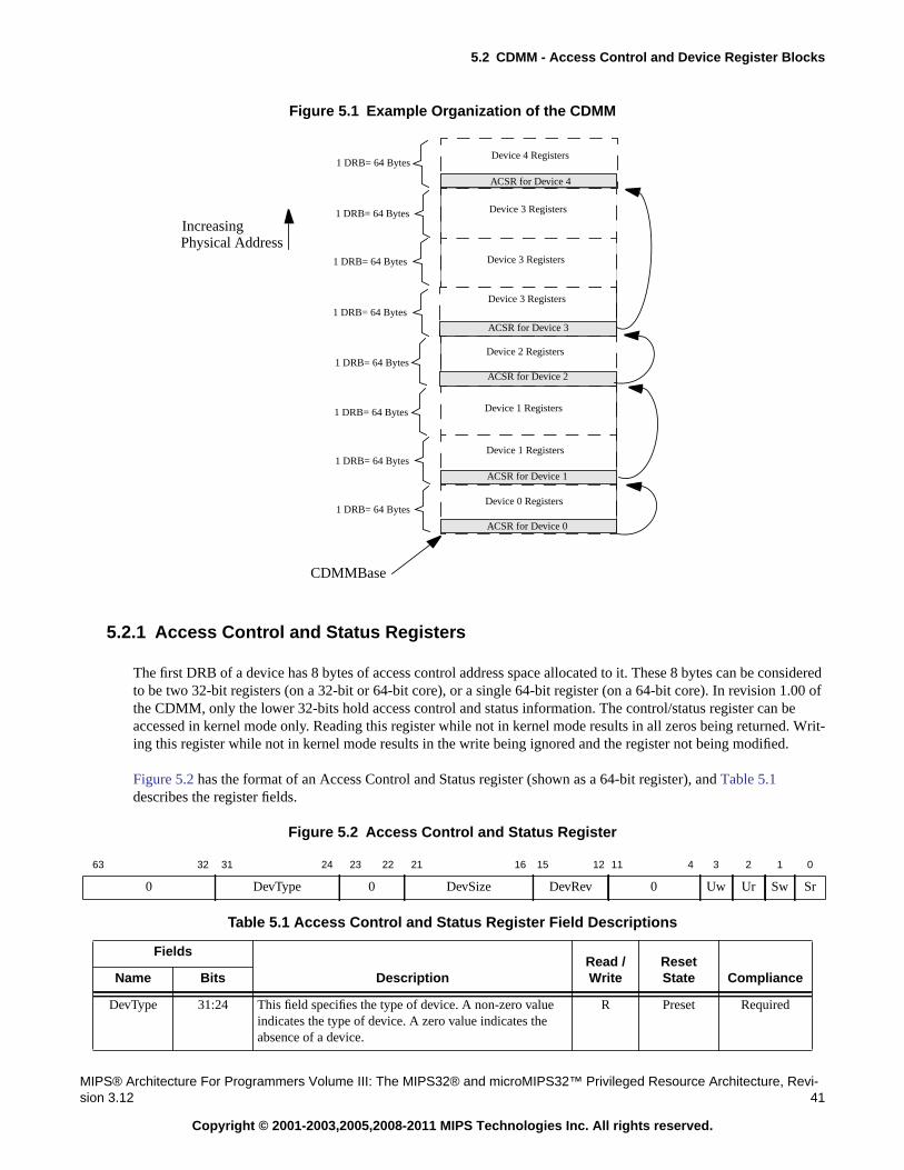
5.2 CDMM - Access Control and Device Register Blocks
MIPS® Architecture For Programmers Volume III: The MIPS32® and microMIPS32™ Privileged Resource Architecture, Revi-sion 3.12 41
Copyright © 2001-2003,2005,2008-2011 MIPS Technologies Inc. All rights reserved.
Figure 5.1 Example Organization of the CDMM
5.2.1 Access Control and Status Registers
The first DRB of a device has 8 bytes of access control address space allocated to it. These 8 bytes can be consideredto be two 32-bit registers (on a 32-bit or 64-bit core), or a single 64-bit register (on a 64-bit core). In revision 1.00 ofthe CDMM, only the lower 32-bits hold access control and status information. The control/status register can beaccessed in kernel mode only. Reading this register while not in kernel mode results in all zeros being returned. Writ-ing this register while not in kernel mode results in the write being ignored and the register not being modified.
Figure 5.2 has the format of an Access Control and Status register (shown as a 64-bit register), and Table 5.1describes the register fields.
Figure 5.2 Access Control and Status Register
63 32 31 24 23 22 21 16 15 12 11 4 3 2 1 0
0 DevType 0 DevSize DevRev 0 Uw Ur Sw Sr
Table 5.1 Access Control and Status Register Field Descriptions
Fields
DescriptionRead /Write
ResetState ComplianceName Bits
DevType 31:24 This field specifies the type of device. A non-zero valueindicates the type of device. A zero value indicates theabsence of a device.
R Preset Required
CDMMBase
IncreasingPhysical Address
ACSR for Device 0
ACSR for Device 1
Device 0 Registers
Device 1 Registers
Device 1 Registers
ACSR for Device 2
Device 2 Registers
ACSR for Device 3
Device 3 Registers
Device 3 Registers
Device 3 Registers
ACSR for Device 4
Device 4 Registers
1 DRB= 64 Bytes
1 DRB= 64 Bytes
1 DRB= 64 Bytes
1 DRB= 64 Bytes
1 DRB= 64 Bytes
1 DRB= 64 Bytes
1 DRB= 64 Bytes
1 DRB= 64 Bytes
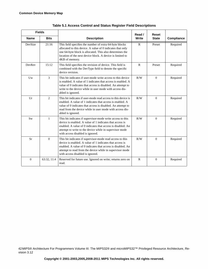
Common Device Memory Map
42MIPS® Architecture For Programmers Volume III: The MIPS32® and microMIPS32™ Privileged Resource Architecture, Re-vision 3.12
Copyright © 2001-2003,2005,2008-2011 MIPS Technologies Inc. All rights reserved.
DevSize 21:16 This field specifies the number of extra 64-byte blocksallocated to this device. A value of 0 indicates that onlyone 64-byte block is allocated. This also determines thelocation of the next device block. A device is limited to4KB of memory.
R Preset Required
DevRev 15:12 This field specifies the revision of device. This field iscombined with the DevType field to denote the specificdevice revision.
R Preset Required
Uw 3 This bit indicates if user-mode write access to this deviceis enabled. A value of 1 indicates that access is enabled. Avalue of 0 indicates that access is disabled. An attempt towrite to the device while in user mode with access dis-abled is ignored.
R/W 0 Required
Ur 2 This bit indicates if user-mode read access to this device isenabled. A value of 1 indicates that access is enabled. Avalue of 0 indicates that access is disabled. An attempt toread from the device while in user mode with access dis-abled is ignored.
R/W 0 Required
Sw 1 This bit indicates if supervisor-mode write access to thisdevice is enabled. A value of 1 indicates that access isenabled. A value of 0 indicates that access is disabled. Anattempt to write to the device while in supervisor modewith access disabled is ignored.
R/W 0 Required
Sr 0 This bit indicates if supervisor-mode read access to thisdevice is enabled. A value of 1 indicates that access isenabled. A value of 0 indicates that access is disabled. Anattempt to read from the device while in supervisor modewith access disabled is ignored.
R/W 0 Required
0 63:32, 11:4 Reserved for future use. Ignored on write; returns zero onread.
R 0 Required
Table 5.1 Access Control and Status Register Field Descriptions
Fields
DescriptionRead /Write
ResetState ComplianceName Bits
Chapter 6
MIPS® Architecture For Programmers Volume III: The MIPS32® and microMIPS32™ Privileged Resource Architecture, Revi-sion 3.12 43
Copyright © 2001-2003,2005,2008-2011 MIPS Technologies Inc. All rights reserved.
Interrupts and Exceptions
Release 2 of the Architecture added the following features related to the processing of Exceptions and Interrupts:
• The addition of the Coprocessor 0 EBase register, which allows the exception vector base address to be modi-fied for exceptions that occur when StatusBEV equals 0. The EBase register is required.
• The extension of the Release 1 interrupt control mechanism to include two optional interrupt modes:
• Vectored Interrupt (VI) mode, in which the various sources of interrupts are prioritized by the processor andeach interrupt is vectored directly to a dedicated handler. When combined with GPR shadow registers, intro-duced in the next chapter, this mode significantly reduces the number of cycles required to process an inter-rupt.
• External Interrupt Controller (EIC) mode, in which the definition of the coprocessor 0 register fields associ-ated with interrupts changes to support an external interrupt controller. This can support many more priori-tized interrupts, while still providing the ability to vector an interrupt directly to a dedicated handler and takeadvantage of the GPR shadow registers.
• The ability to stop the Count register for highly power-sensitive applications in which the Count register is notused, or for reduced power mode. This change is required.
• The addition of the DI and EI instructions which provide the ability to atomically disable or enable interrupts.Both instructions are required.
• The addition of the TI and PCI bits in the Cause register to denote pending timer and performance counter inter-rupts. This change is required.
• The addition of an execution hazard sequence which can be used to clear hazards introduced when softwarewrites to a coprocessor 0 register which affects the interrupt system state.
6.1 Interrupts
Release 1 of the Architecture included support for two software interrupts, six hardware interrupts, and two spe-cial-purpose interrupts: timer and performance counter. The timer and performance counter interrupts were combinedwith hardware interrupt 5 in an implementation-dependent manner. Interrupts were handled either through the generalexception vector (offset 0x180) or the special interrupt vector (0x200), based on the value of CauseIV. Software wasrequired to prioritize interrupts as a function of the CauseIP bits in the interrupt handler prologue.
Release 2 of the Architecture adds an upward-compatible extension to the Release 1 interrupt architecture that sup-ports vectored interrupts. In addition, Release 2 adds a new interrupt mode that supports the use of an external inter-rupt controller by changing the interrupt architecture.
Although a Non-Maskable Interrupt (NMI) includes “interrupt” in its name, it is more correctly described as an NMIexception because it does not affect, nor is it controlled by the processor interrupt system.
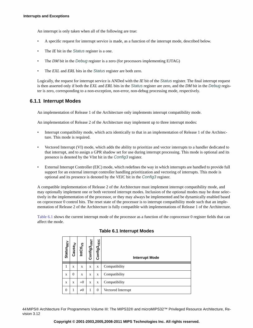
Interrupts and Exceptions
44MIPS® Architecture For Programmers Volume III: The MIPS32® and microMIPS32™ Privileged Resource Architecture, Re-vision 3.12
Copyright © 2001-2003,2005,2008-2011 MIPS Technologies Inc. All rights reserved.
An interrupt is only taken when all of the following are true:
• A specific request for interrupt service is made, as a function of the interrupt mode, described below.
• The IE bit in the Status register is a one.
• The DM bit in the Debug register is a zero (for processors implementing EJTAG)
• The EXL and ERL bits in the Status register are both zero.
Logically, the request for interrupt service is ANDed with the IE bit of the Status register. The final interrupt requestis then asserted only if both the EXL and ERL bits in the Status register are zero, and the DM bit in the Debug regis-ter is zero, corresponding to a non-exception, non-error, non-debug processing mode, respectively.
6.1.1 Interrupt Modes
An implementation of Release 1 of the Architecture only implements interrupt compatibility mode.
An implementation of Release 2 of the Architecture may implement up to three interrupt modes:
• Interrupt compatibility mode, which acts identically to that in an implementation of Release 1 of the Architec-ture. This mode is required.
• Vectored Interrupt (VI) mode, which adds the ability to prioritize and vector interrupts to a handler dedicated tothat interrupt, and to assign a GPR shadow set for use during interrupt processing. This mode is optional and itspresence is denoted by the VInt bit in the Config3 register.
• External Interrupt Controller (EIC) mode, which redefines the way in which interrupts are handled to provide fullsupport for an external interrupt controller handling prioritization and vectoring of interrupts. This mode isoptional and its presence is denoted by the VEIC bit in the Config3 register.
A compatible implementation of Release 2 of the Architecture must implement interrupt compatibility mode, andmay optionally implement one or both vectored interrupt modes. Inclusion of the optional modes may be done selec-tively in the implementation of the processor, or they may always be implemented and be dynamically enabled basedon coprocessor 0 control bits. The reset state of the processor is to interrupt compatibility mode such that an imple-mentation of Release 2 of the Architecture is fully compatible with implementations of Release 1 of the Architecture.
Table 6.1 shows the current interrupt mode of the processor as a function of the coprocessor 0 register fields that canaffect the mode.
Table 6.1 Interrupt Modes
Sta
tus B
EV
Cau
seIV
IntC
tlV
S
Co
nfi
g3 V
INT
Co
nfi
g3 V
EIC
Interrupt Mode
1 x x x x Compatibility
x 0 x x x Compatibility
x x =0 x x Compatibility
0 1 ≠0 1 0 Vectored Interrupt
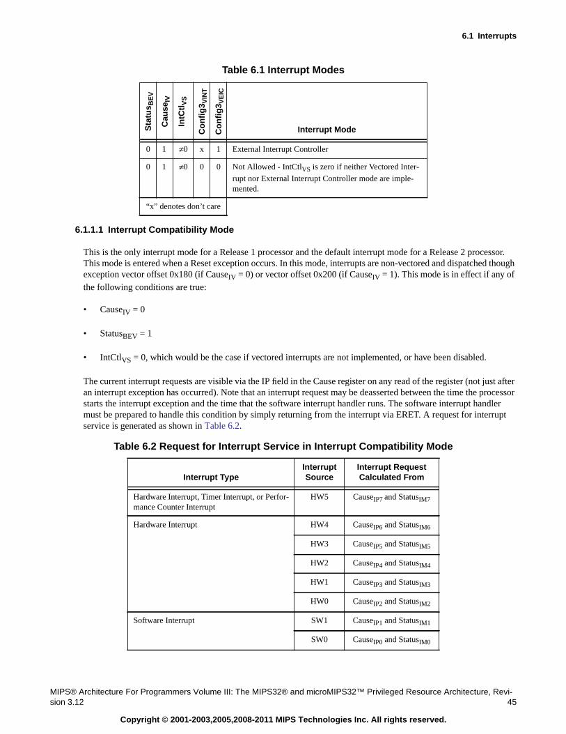
6.1 Interrupts
MIPS® Architecture For Programmers Volume III: The MIPS32® and microMIPS32™ Privileged Resource Architecture, Revi-sion 3.12 45
Copyright © 2001-2003,2005,2008-2011 MIPS Technologies Inc. All rights reserved.
6.1.1.1 Interrupt Compatibility Mode
This is the only interrupt mode for a Release 1 processor and the default interrupt mode for a Release 2 processor.This mode is entered when a Reset exception occurs. In this mode, interrupts are non-vectored and dispatched thoughexception vector offset 0x180 (if CauseIV = 0) or vector offset 0x200 (if CauseIV = 1). This mode is in effect if any ofthe following conditions are true:
• CauseIV = 0
• StatusBEV = 1
• IntCtlVS = 0, which would be the case if vectored interrupts are not implemented, or have been disabled.
The current interrupt requests are visible via the IP field in the Cause register on any read of the register (not just afteran interrupt exception has occurred). Note that an interrupt request may be deasserted between the time the processorstarts the interrupt exception and the time that the software interrupt handler runs. The software interrupt handlermust be prepared to handle this condition by simply returning from the interrupt via ERET. A request for interruptservice is generated as shown in Table 6.2.
0 1 ≠0 x 1 External Interrupt Controller
0 1 ≠0 0 0 Not Allowed - IntCtlVS is zero if neither Vectored Inter-
rupt nor External Interrupt Controller mode are imple-mented.
“x” denotes don’t care
Table 6.2 Request for Interrupt Service in Interrupt Compatibility Mode
Interrupt TypeInterruptSource
Interrupt RequestCalculated From
Hardware Interrupt, Timer Interrupt, or Perfor-mance Counter Interrupt
HW5 CauseIP7 and StatusIM7
Hardware Interrupt HW4 CauseIP6 and StatusIM6
HW3 CauseIP5 and StatusIM5
HW2 CauseIP4 and StatusIM4
HW1 CauseIP3 and StatusIM3
HW0 CauseIP2 and StatusIM2
Software Interrupt SW1 CauseIP1 and StatusIM1
SW0 CauseIP0 and StatusIM0
Table 6.1 Interrupt Modes
Sta
tus B
EV
Cau
seIV
IntC
tlV
S
Co
nfi
g3 V
INT
Co
nfi
g3 V
EIC
Interrupt Mode
Interrupts and Exceptions
46MIPS® Architecture For Programmers Volume III: The MIPS32® and microMIPS32™ Privileged Resource Architecture, Re-vision 3.12
Copyright © 2001-2003,2005,2008-2011 MIPS Technologies Inc. All rights reserved.
A typical software handler for interrupt compatibility mode might look as follows:
/* * Assumptions: * - CauseIV = 1 (if it were zero, the interrupt exception would have to * be isolated from the general exception vector before getting * here) * - GPRs k0 and k1 are available (no shadow register switches invoked in * compatibility mode) * - The software priority is IP7..IP0 (HW5..HW0, SW1..SW0) * * Location: Offset 0x200 from exception base */
IVexception:mfc0 k0, C0_Cause /* Read Cause register for IP bits */mfc0 k1, C0_Status /* and Status register for IM bits */andi k0, k0, M_CauseIM /* Keep only IP bits from Cause */and k0, k0, k1 /* and mask with IM bits */beq k0, zero, Dismiss /* no bits set - spurious interrupt */clz k0, k0 /* Find first bit set, IP7..IP0; k0 = 16..23 */xori k0, k0, 0x17 /* 16..23 => 7..0 */sll k0, k0, VS /* Shift to emulate software IntCtlVS */la k1, VectorBase /* Get base of 8 interrupt vectors */addu k0, k0, k1 /* Compute target from base and offset */jr k0 /* Jump to specific exception routine */nop
/* * Each interrupt processing routine processes a specific interrupt, analogous * to those reached in VI or EIC interrupt mode. Since each processing routine * is dedicated to a particular interrupt line, it has the context to know * which line was asserted. Each processing routine may need to look further * to determine the actual source of the interrupt if multiple interrupt requests * are ORed together on a single IP line. Once that task is performed, the * interrupt may be processed in one of two ways: * * - Completely at interrupt level (e.g., a simply UART interrupt). The * SimpleInterrupt routine below is an example of this type. * - By saving sufficient state and re-enabling other interrupts. In this * case the software model determines which interrupts are disabled during * the processing of this interrupt. Typically, this is either the single * StatusIM bit that corresponds to the interrupt being processed, or some * collection of other StatusIM bits so that “lower” priority interrupts are * also disabled. The NestedInterrupt routine below is an example of this type. */
SimpleInterrupt:/* * Process the device interrupt here and clear the interupt request * at the device. In order to do this, some registers may need to be * saved and restored. The coprocessor 0 state is such that an ERET * will simply return to the interrupted code. */
eret /* Return to interrupted code */
NestedException:/*
6.1 Interrupts
MIPS® Architecture For Programmers Volume III: The MIPS32® and microMIPS32™ Privileged Resource Architecture, Revi-sion 3.12 47
Copyright © 2001-2003,2005,2008-2011 MIPS Technologies Inc. All rights reserved.
* Nested exceptions typically require saving the EPC and Status registers, * any GPRs that may be modified by the nested exception routine, disabling * the appropriate IM bits in Status to prevent an interrupt loop, putting * the processor in kernel mode, and re-enabling interrupts. The sample code * below can not cover all nuances of this processing and is intended only * to demonstrate the concepts. */
/* Save GPRs here, and setup software context */mfc0 k0, C0_EPC /* Get restart address */sw k0, EPCSave /* Save in memory */mfc0 k0, C0_Status /* Get Status value */sw k0, StatusSave /* Save in memory */li k1, ~IMbitsToClear /* Get Im bits to clear for this interrupt */
/* this must include at least the IM bit *//* for the current interrupt, and may include *//* others */
and k0, k0, k1 /* Clear bits in copy of Status */ins k0, zero, S_StatusEXL, (W_StatusKSU+W_StatusERL+W_StatusEXL)
/* Clear KSU, ERL, EXL bits in k0 */mtc0 k0, C0_Status /* Modify mask, switch to kernel mode, */
/* re-enable interrupts */
/* * Process interrupt here, including clearing device interrupt. * In some environments this may be done with a thread running in * kernel or user mode. Such an environment is well beyond the scope of * this example. */
/* * To complete interrupt processing, the saved values must be restored * and the original interrupted code restarted. */
di /* Disable interrupts - may not be required */lw k0, StatusSave /* Get saved Status (including EXL set) */lw k1, EPCSave /* and EPC */mtc0 k0, C0_Status /* Restore the original value */mtc0 k1, C0_EPC /* and EPC *//* Restore GPRs and software state */eret /* Dismiss the interrupt */
6.1.1.2 Vectored Interrupt Mode
Vectored Interrupt mode builds on the interrupt compatibility mode by adding a priority encoder to prioritize pendinginterrupts and to generate a vector with which each interrupt can be directed to a dedicated handler routine. Thismode also allows each interrupt to be mapped to a GPR shadow set for use by the interrupt handler. Vectored Interruptmode is in effect if all of the following conditions are true:
• Config3VInt = 1
• Config3VEIC = 0
• IntCtlVS ≠ 0
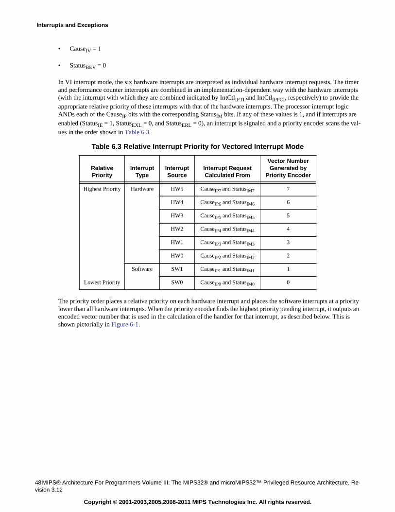
Interrupts and Exceptions
48MIPS® Architecture For Programmers Volume III: The MIPS32® and microMIPS32™ Privileged Resource Architecture, Re-vision 3.12
Copyright © 2001-2003,2005,2008-2011 MIPS Technologies Inc. All rights reserved.
• CauseIV = 1
• StatusBEV = 0
In VI interrupt mode, the six hardware interrupts are interpreted as individual hardware interrupt requests. The timerand performance counter interrupts are combined in an implementation-dependent way with the hardware interrupts(with the interrupt with which they are combined indicated by IntCtlIPTI and IntCtlIPPCI, respectively) to provide theappropriate relative priority of these interrupts with that of the hardware interrupts. The processor interrupt logicANDs each of the CauseIP bits with the corresponding StatusIM bits. If any of these values is 1, and if interrupts areenabled (StatusIE = 1, StatusEXL = 0, and StatusERL = 0), an interrupt is signaled and a priority encoder scans the val-ues in the order shown in Table 6.3.
The priority order places a relative priority on each hardware interrupt and places the software interrupts at a prioritylower than all hardware interrupts. When the priority encoder finds the highest priority pending interrupt, it outputs anencoded vector number that is used in the calculation of the handler for that interrupt, as described below. This isshown pictorially in Figure 6-1.
Table 6.3 Relative Interrupt Priority for Vectored Interrupt Mode
RelativePriority
InterruptType
InterruptSource
Interrupt RequestCalculated From
Vector NumberGenerated by
Priority Encoder
Highest Priority Hardware HW5 CauseIP7 and StatusIM7 7
HW4 CauseIP6 and StatusIM6 6
HW3 CauseIP5 and StatusIM5 5
HW2 CauseIP4 and StatusIM4 4
HW1 CauseIP3 and StatusIM3 3
HW0 CauseIP2 and StatusIM2 2
Software SW1 CauseIP1 and StatusIM1 1
Lowest Priority SW0 CauseIP0 and StatusIM0 0
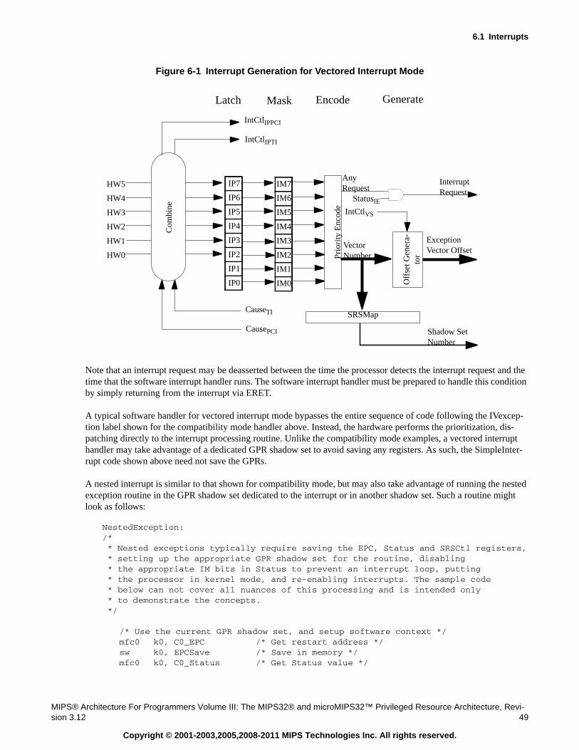
6.1 Interrupts
MIPS® Architecture For Programmers Volume III: The MIPS32® and microMIPS32™ Privileged Resource Architecture, Revi-sion 3.12 49
Copyright © 2001-2003,2005,2008-2011 MIPS Technologies Inc. All rights reserved.
Figure 6-1 Interrupt Generation for Vectored Interrupt Mode
Note that an interrupt request may be deasserted between the time the processor detects the interrupt request and thetime that the software interrupt handler runs. The software interrupt handler must be prepared to handle this conditionby simply returning from the interrupt via ERET.
A typical software handler for vectored interrupt mode bypasses the entire sequence of code following the IVexcep-tion label shown for the compatibility mode handler above. Instead, the hardware performs the prioritization, dis-patching directly to the interrupt processing routine. Unlike the compatibility mode examples, a vectored interrupthandler may take advantage of a dedicated GPR shadow set to avoid saving any registers. As such, the SimpleInter-rupt code shown above need not save the GPRs.
A nested interrupt is similar to that shown for compatibility mode, but may also take advantage of running the nestedexception routine in the GPR shadow set dedicated to the interrupt or in another shadow set. Such a routine mightlook as follows:
NestedException:/* * Nested exceptions typically require saving the EPC, Status and SRSCtl registers, * setting up the appropriate GPR shadow set for the routine, disabling * the appropriate IM bits in Status to prevent an interrupt loop, putting * the processor in kernel mode, and re-enabling interrupts. The sample code * below can not cover all nuances of this processing and is intended only * to demonstrate the concepts. */
/* Use the current GPR shadow set, and setup software context */mfc0 k0, C0_EPC /* Get restart address */sw k0, EPCSave /* Save in memory */mfc0 k0, C0_Status /* Get Status value */
IP7
IP6
IP5
IP4
IP3
IP2
IP1
IP0
IM7
IM6
IM5
IM4
IM3
IM2
IM1
IM0
Prio
rity
Enc
ode
HW5
HW4
HW3
HW2
HW1
HW0
Com
bine
CauseTI
CausePCI
StatusIE
InterruptRequest
VectorNumber
Latch Mask Encode
AnyRequest
Off
set G
ener
a-to
r
IntCtlVS
ExceptionVector Offset
Generate
SRSMap
Shadow SetNumber
IntCtlIPPCI
IntCtlIPTI
Interrupts and Exceptions
50MIPS® Architecture For Programmers Volume III: The MIPS32® and microMIPS32™ Privileged Resource Architecture, Re-vision 3.12
Copyright © 2001-2003,2005,2008-2011 MIPS Technologies Inc. All rights reserved.
sw k0, StatusSave /* Save in memory */mfc0 k0, C0_SRSCtl /* Save SRSCtl if changing shadow sets */sw k0, SRSCtlSaveli k1, ~IMbitsToClear /* Get Im bits to clear for this interrupt */
/* this must include at least the IM bit *//* for the current interrupt, and may include *//* others */
and k0, k0, k1 /* Clear bits in copy of Status *//* If switching shadow sets, write new value to SRSCtlPSS here */ins k0, zero, S_StatusEXL, (W_StatusKSU+W_StatusERL+W_StatusEXL)
/* Clear KSU, ERL, EXL bits in k0 */mtc0 k0, C0_Status /* Modify mask, switch to kernel mode, */
/* re-enable interrupts *//* * If switching shadow sets, clear only KSU above, write target * address to EPC, and do execute an eret to clear EXL, switch * shadow sets, and jump to routine */
/* Process interrupt here, including clearing device interrupt */
/* * To complete interrupt processing, the saved values must be restored * and the original interrupted code restarted. */
di /* Disable interrupts - may not be required */lw k0, StatusSave /* Get saved Status (including EXL set) */lw k1, EPCSave /* and EPC */mtc0 k0, C0_Status /* Restore the original value */lw k0, SRSCtlSave /* Get saved SRSCtl */mtc0 k1, C0_EPC /* and EPC */mtc0 k0, C0_SRSCtl /* Restore shadow sets */ehb /* Clear hazard */eret /* Dismiss the interrupt */
6.1.1.3 External Interrupt Controller Mode
External Interrupt Controller Mode redefines the way that the processor interrupt logic is configured to provide sup-port for an external interrupt controller. The interrupt controller is responsible for prioritizing all interrupts, includinghardware, software, timer, and performance counter interrupts, and directly supplying to the processor the vectornumber (and optionally the priority level) of the highest priority interrupt. EIC interrupt mode is in effect if all of thefollowing conditions are true:
• Config3VEIC = 1
• IntCtlVS ≠ 0
• CauseIV = 1
• StatusBEV = 0
In EIC interrupt mode, the processor sends the state of the software interrupt requests (CauseIP1..IP0), the timer inter-rupt request (CauseTI), and the performance counter interrupt request (CausePCI) to the external interrupt controller,where it prioritizes these interrupts in a system-dependent way with other hardware interrupts. The interrupt control-
6.1 Interrupts
MIPS® Architecture For Programmers Volume III: The MIPS32® and microMIPS32™ Privileged Resource Architecture, Revi-sion 3.12 51
Copyright © 2001-2003,2005,2008-2011 MIPS Technologies Inc. All rights reserved.
ler can be a hard-wired logic block, or it can be configurable based on control and status registers. This allows theinterrupt controller to be more specific or more general as a function of the system environment and needs.
The external interrupt controller prioritizes its interrupt requests and produces the priority level and the vector numberof the highest priority interrupt to be serviced. The priority level, called the Requested Interrupt Priority Level(RIPL), is a 6-bit encoded value in the range 0..63, inclusive. A value of 0 indicates that no interrupt requests arepending. The values 1..63 represent the lowest (1) to highest (63) RIPL for the interrupt to be serviced. The interruptcontroller passes this value on the 6 hardware interrupt lines, which are treated as an encoded value in EIC interruptmode. There are several implementation options available for the vector offset:
1. The first option is to treat the RIPL value as the vector number for the processor.
2. The second option is to send a separate vector number along with the RIPL to the processor.
3. A third option is to send an entire vector offset along with the RIPL to the processor.
StatusIPL (which overlays StatusIM7..IM2) is interpreted as the Interrupt Priority Level (IPL) at which the processor iscurrently operating (with a value of zero indicating that no interrupt is currently being serviced). When the interruptcontroller requests service for an interrupt, the processor compares RIPL with StatusIPL to determine if the requestedinterrupt has higher priority than the current IPL. If RIPL is strictly greater than StatusIPL, and interrupts are enabled(StatusIE = 1, StatusEXL = 0, and StatusERL = 0) an interrupt request is signaled to the pipeline. When the processorstarts the interrupt exception, it loads RIPL into CauseRIPL (which overlays CauseIP7..IP2) and signals the externalinterrupt controller to notify it that the request is being serviced. Because CauseRIPL is only loaded by the processorwhen an interrupt exception is signaled, it is available to software during interrupt processing. The vector number thatthe EIC passes into the core is combined with the IntCtlVS to determine where the interrupt service routines islocated. The vector number is not stored in any software visible register. Some implementations may choose to usethe RIPL as the vector number, but this is not a requirement.
In EIC interrupt mode, the external interrupt controller is also responsible for supplying the GPR shadow set numberto use when servicing the interrupt. As such, the SRSMap register is not used in this mode, and the mapping of thevectored interrupt to a GPR shadow set is done by programming (or designing) the interrupt controller to provide thecorrect GPR shadow set number when an interrupt is requested. When the processor loads an interrupt request intoCauseRIPL, it also loads the GPR shadow set number into SRSCtlEICSS, which is copied to SRSCtlCSS when the inter-rupt is serviced.
The operation of EIC interrupt mode is shown pictorially in Figure 6-2.
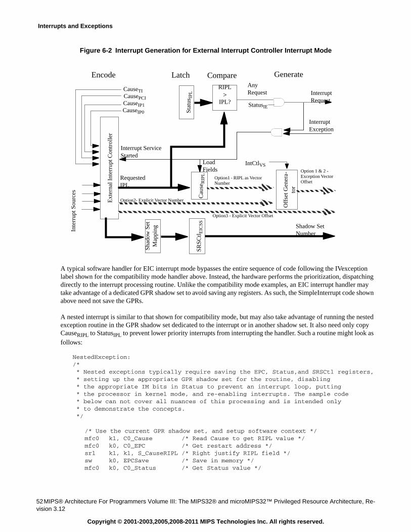
Interrupts and Exceptions
52MIPS® Architecture For Programmers Volume III: The MIPS32® and microMIPS32™ Privileged Resource Architecture, Re-vision 3.12
Copyright © 2001-2003,2005,2008-2011 MIPS Technologies Inc. All rights reserved.
Figure 6-2 Interrupt Generation for External Interrupt Controller Interrupt Mode
A typical software handler for EIC interrupt mode bypasses the entire sequence of code following the IVexceptionlabel shown for the compatibility mode handler above. Instead, the hardware performs the prioritization, dispatchingdirectly to the interrupt processing routine. Unlike the compatibility mode examples, an EIC interrupt handler maytake advantage of a dedicated GPR shadow set to avoid saving any registers. As such, the SimpleInterrupt code shownabove need not save the GPRs.
A nested interrupt is similar to that shown for compatibility mode, but may also take advantage of running the nestedexception routine in the GPR shadow set dedicated to the interrupt or in another shadow set. It also need only copyCauseRIPL to StatusIPL to prevent lower priority interrupts from interrupting the handler. Such a routine might look asfollows:
NestedException:/* * Nested exceptions typically require saving the EPC, Status,and SRSCtl registers, * setting up the appropriate GPR shadow set for the routine, disabling * the appropriate IM bits in Status to prevent an interrupt loop, putting * the processor in kernel mode, and re-enabling interrupts. The sample code * below can not cover all nuances of this processing and is intended only * to demonstrate the concepts. */
/* Use the current GPR shadow set, and setup software context */mfc0 k1, C0_Cause /* Read Cause to get RIPL value */mfc0 k0, C0_EPC /* Get restart address */srl k1, k1, S_CauseRIPL /* Right justify RIPL field */sw k0, EPCSave /* Save in memory */mfc0 k0, C0_Status /* Get Status value */
CauseTICausePCI
StatusIE
InterruptRequest
Option1 - RIPL as VectorNumber
Latch CompareEncodeAnyRequest
Off
set G
ener
a-to
r
IntCtlVSOption 1 & 2 -Exception VectorOffset
Generate
Shadow SetNumber
Ext
erna
l Int
erru
pt C
ontr
olle
r
Inte
rrup
t Sou
rces
Shad
ow S
etM
appi
ng
CauseIP1CauseIP0
RequestedIPL
Cau
seR
IPL
Stat
usIP
L
SRSC
tl EIC
SS
RIPL>
IPL?
LoadFields
InterruptException
Interrupt ServiceStarted
Option2- Explicit Vector Number
Option3 - Explicit Vector Offset
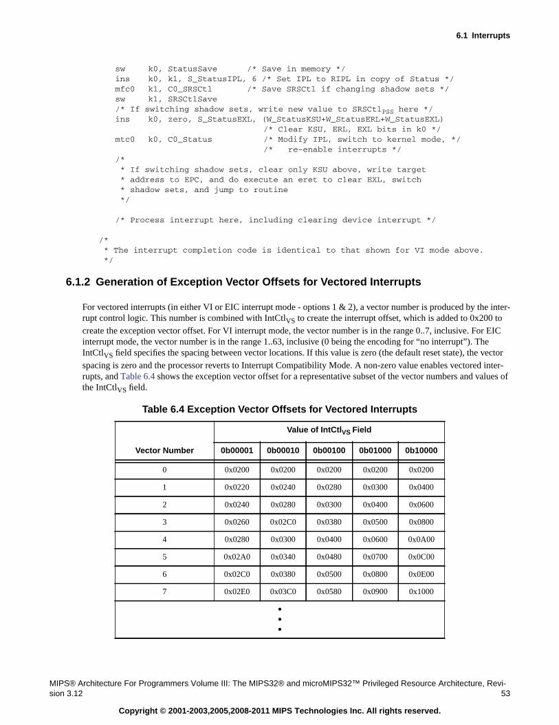
6.1 Interrupts
MIPS® Architecture For Programmers Volume III: The MIPS32® and microMIPS32™ Privileged Resource Architecture, Revi-sion 3.12 53
Copyright © 2001-2003,2005,2008-2011 MIPS Technologies Inc. All rights reserved.
sw k0, StatusSave /* Save in memory */ins k0, k1, S_StatusIPL, 6 /* Set IPL to RIPL in copy of Status */mfc0 k1, C0_SRSCtl /* Save SRSCtl if changing shadow sets */sw k1, SRSCtlSave/* If switching shadow sets, write new value to SRSCtlPSS here */ins k0, zero, S_StatusEXL, (W_StatusKSU+W_StatusERL+W_StatusEXL)
/* Clear KSU, ERL, EXL bits in k0 */mtc0 k0, C0_Status /* Modify IPL, switch to kernel mode, */
/* re-enable interrupts *//* * If switching shadow sets, clear only KSU above, write target * address to EPC, and do execute an eret to clear EXL, switch * shadow sets, and jump to routine */
/* Process interrupt here, including clearing device interrupt */
/* * The interrupt completion code is identical to that shown for VI mode above. */
6.1.2 Generation of Exception Vector Offsets for Vectored Interrupts
For vectored interrupts (in either VI or EIC interrupt mode - options 1 & 2), a vector number is produced by the inter-rupt control logic. This number is combined with IntCtlVS to create the interrupt offset, which is added to 0x200 tocreate the exception vector offset. For VI interrupt mode, the vector number is in the range 0..7, inclusive. For EICinterrupt mode, the vector number is in the range 1..63, inclusive (0 being the encoding for “no interrupt”). TheIntCtlVS field specifies the spacing between vector locations. If this value is zero (the default reset state), the vectorspacing is zero and the processor reverts to Interrupt Compatibility Mode. A non-zero value enables vectored inter-rupts, and Table 6.4 shows the exception vector offset for a representative subset of the vector numbers and values ofthe IntCtlVS field.
Table 6.4 Exception Vector Offsets for Vectored Interrupts
Vector Number
Value of IntCtlVS Field
0b00001 0b00010 0b00100 0b01000 0b10000
0 0x0200 0x0200 0x0200 0x0200 0x0200
1 0x0220 0x0240 0x0280 0x0300 0x0400
2 0x0240 0x0280 0x0300 0x0400 0x0600
3 0x0260 0x02C0 0x0380 0x0500 0x0800
4 0x0280 0x0300 0x0400 0x0600 0x0A00
5 0x02A0 0x0340 0x0480 0x0700 0x0C00
6 0x02C0 0x0380 0x0500 0x0800 0x0E00
7 0x02E0 0x03C0 0x0580 0x0900 0x1000
•••
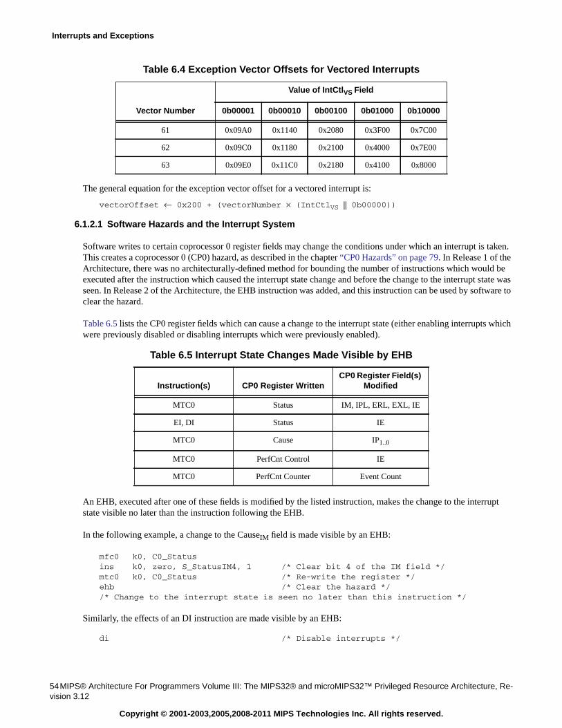
Interrupts and Exceptions
54MIPS® Architecture For Programmers Volume III: The MIPS32® and microMIPS32™ Privileged Resource Architecture, Re-vision 3.12
Copyright © 2001-2003,2005,2008-2011 MIPS Technologies Inc. All rights reserved.
The general equation for the exception vector offset for a vectored interrupt is:
vectorOffset ← 0x200 + (vectorNumber × (IntCtlVS || 0b00000))
6.1.2.1 Software Hazards and the Interrupt System
Software writes to certain coprocessor 0 register fields may change the conditions under which an interrupt is taken.This creates a coprocessor 0 (CP0) hazard, as described in the chapter “CP0 Hazards” on page 79. In Release 1 of theArchitecture, there was no architecturally-defined method for bounding the number of instructions which would beexecuted after the instruction which caused the interrupt state change and before the change to the interrupt state wasseen. In Release 2 of the Architecture, the EHB instruction was added, and this instruction can be used by software toclear the hazard.
Table 6.5 lists the CP0 register fields which can cause a change to the interrupt state (either enabling interrupts whichwere previously disabled or disabling interrupts which were previously enabled).
An EHB, executed after one of these fields is modified by the listed instruction, makes the change to the interruptstate visible no later than the instruction following the EHB.
In the following example, a change to the CauseIM field is made visible by an EHB:
mfc0 k0, C0_Statusins k0, zero, S_StatusIM4, 1 /* Clear bit 4 of the IM field */mtc0 k0, C0_Status /* Re-write the register */ehb /* Clear the hazard *//* Change to the interrupt state is seen no later than this instruction */
Similarly, the effects of an DI instruction are made visible by an EHB:
di /* Disable interrupts */
61 0x09A0 0x1140 0x2080 0x3F00 0x7C00
62 0x09C0 0x1180 0x2100 0x4000 0x7E00
63 0x09E0 0x11C0 0x2180 0x4100 0x8000
Table 6.5 Interrupt State Changes Made Visible by EHB
Instruction(s) CP0 Register WrittenCP0 Register Field(s)
Modified
MTC0 Status IM, IPL, ERL, EXL, IE
EI, DI Status IE
MTC0 Cause IP1..0
MTC0 PerfCnt Control IE
MTC0 PerfCnt Counter Event Count
Table 6.4 Exception Vector Offsets for Vectored Interrupts
Vector Number
Value of IntCtlVS Field
0b00001 0b00010 0b00100 0b01000 0b10000
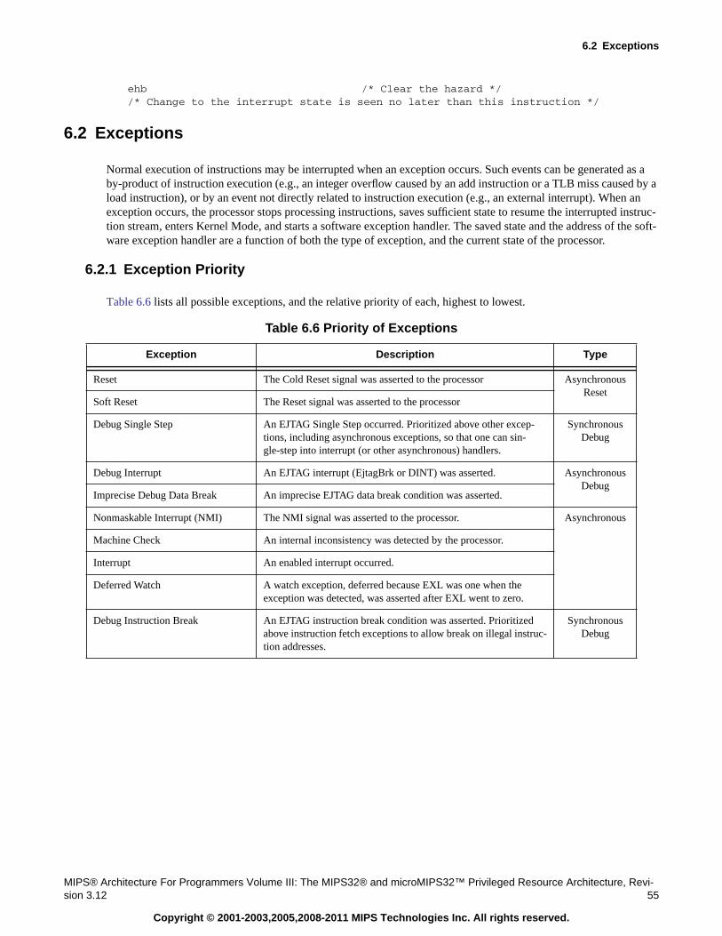
6.2 Exceptions
MIPS® Architecture For Programmers Volume III: The MIPS32® and microMIPS32™ Privileged Resource Architecture, Revi-sion 3.12 55
Copyright © 2001-2003,2005,2008-2011 MIPS Technologies Inc. All rights reserved.
ehb /* Clear the hazard *//* Change to the interrupt state is seen no later than this instruction */
6.2 Exceptions
Normal execution of instructions may be interrupted when an exception occurs. Such events can be generated as aby-product of instruction execution (e.g., an integer overflow caused by an add instruction or a TLB miss caused by aload instruction), or by an event not directly related to instruction execution (e.g., an external interrupt). When anexception occurs, the processor stops processing instructions, saves sufficient state to resume the interrupted instruc-tion stream, enters Kernel Mode, and starts a software exception handler. The saved state and the address of the soft-ware exception handler are a function of both the type of exception, and the current state of the processor.
6.2.1 Exception Priority
Table 6.6 lists all possible exceptions, and the relative priority of each, highest to lowest.
Table 6.6 Priority of Exceptions
Exception Description Type
Reset The Cold Reset signal was asserted to the processor AsynchronousReset
Soft Reset The Reset signal was asserted to the processor
Debug Single Step An EJTAG Single Step occurred. Prioritized above other excep-tions, including asynchronous exceptions, so that one can sin-gle-step into interrupt (or other asynchronous) handlers.
SynchronousDebug
Debug Interrupt An EJTAG interrupt (EjtagBrk or DINT) was asserted. AsynchronousDebug
Imprecise Debug Data Break An imprecise EJTAG data break condition was asserted.
Nonmaskable Interrupt (NMI) The NMI signal was asserted to the processor. Asynchronous
Machine Check An internal inconsistency was detected by the processor.
Interrupt An enabled interrupt occurred.
Deferred Watch A watch exception, deferred because EXL was one when theexception was detected, was asserted after EXL went to zero.
Debug Instruction Break An EJTAG instruction break condition was asserted. Prioritizedabove instruction fetch exceptions to allow break on illegal instruc-tion addresses.
SynchronousDebug
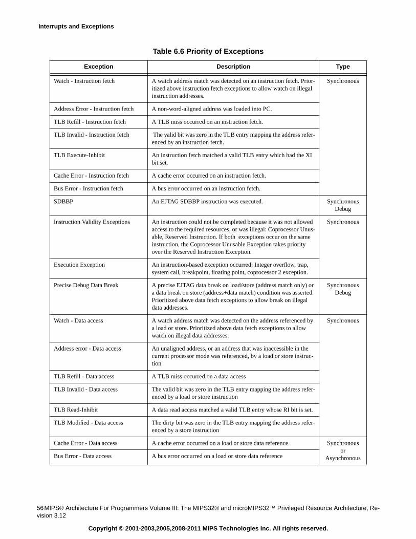
Interrupts and Exceptions
56MIPS® Architecture For Programmers Volume III: The MIPS32® and microMIPS32™ Privileged Resource Architecture, Re-vision 3.12
Copyright © 2001-2003,2005,2008-2011 MIPS Technologies Inc. All rights reserved.
Watch - Instruction fetch A watch address match was detected on an instruction fetch. Prior-itized above instruction fetch exceptions to allow watch on illegalinstruction addresses.
Synchronous
Address Error - Instruction fetch A non-word-aligned address was loaded into PC.
TLB Refill - Instruction fetch A TLB miss occurred on an instruction fetch.
TLB Invalid - Instruction fetch The valid bit was zero in the TLB entry mapping the address refer-enced by an instruction fetch.
TLB Execute-Inhibit An instruction fetch matched a valid TLB entry which had the XIbit set.
Cache Error - Instruction fetch A cache error occurred on an instruction fetch.
Bus Error - Instruction fetch A bus error occurred on an instruction fetch.
SDBBP An EJTAG SDBBP instruction was executed. SynchronousDebug
Instruction Validity Exceptions An instruction could not be completed because it was not allowedaccess to the required resources, or was illegal: Coprocessor Unus-able, Reserved Instruction. If both exceptions occur on the sameinstruction, the Coprocessor Unusable Exception takes priorityover the Reserved Instruction Exception.
Synchronous
Execution Exception An instruction-based exception occurred: Integer overflow, trap,system call, breakpoint, floating point, coprocessor 2 exception.
Precise Debug Data Break A precise EJTAG data break on load/store (address match only) ora data break on store (address+data match) condition was asserted.Prioritized above data fetch exceptions to allow break on illegaldata addresses.
SynchronousDebug
Watch - Data access A watch address match was detected on the address referenced bya load or store. Prioritized above data fetch exceptions to allowwatch on illegal data addresses.
Synchronous
Address error - Data access An unaligned address, or an address that was inaccessible in thecurrent processor mode was referenced, by a load or store instruc-tion
TLB Refill - Data access A TLB miss occurred on a data access
TLB Invalid - Data access The valid bit was zero in the TLB entry mapping the address refer-enced by a load or store instruction
TLB Read-Inhibit A data read access matched a valid TLB entry whose RI bit is set.
TLB Modified - Data access The dirty bit was zero in the TLB entry mapping the address refer-enced by a store instruction
Cache Error - Data access A cache error occurred on a load or store data reference Synchronousor
AsynchronousBus Error - Data access A bus error occurred on a load or store data reference
Table 6.6 Priority of Exceptions
Exception Description Type
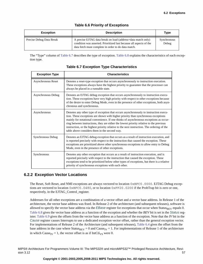
6.2 Exceptions
MIPS® Architecture For Programmers Volume III: The MIPS32® and microMIPS32™ Privileged Resource Architecture, Revi-sion 3.12 57
Copyright © 2001-2003,2005,2008-2011 MIPS Technologies Inc. All rights reserved.
The “Type” column of Table 6.7 describes the type of exception. Table 6.8 explains the characteristics of each excep-tion type.
6.2.2 Exception Vector Locations
The Reset, Soft Reset, and NMI exceptions are always vectored to location 0xBFC0.0000. EJTAG Debug excep-tions are vectored to location 0xBFC0.0480, or to location 0xFF20.0200 if the ProbTrap bit is zero or one,respectively, in the EJTAG_Control_register.
Addresses for all other exceptions are a combination of a vector offset and a vector base address. In Release 1 of thearchitecture, the vector base address was fixed. In Release 2 of the architecture (and subsequent releases), software isallowed to specify the vector base address via the EBase register for exceptions that occur when StatusBEV equals 0.Table 6.8 gives the vector base address as a function of the exception and whether the BEV bit is set in the Status reg-ister. Table 6.9 gives the offsets from the vector base address as a function of the exception. Note that the IV bit in theCause register causes Interrupts to use a dedicated exception vector offset, rather than the general exception vector.For implementations of Release 2 of the Architecture (and subsequent releases), Table 6.4 gives the offset from thebase address in the case where StatusBEV = 0 and CauseIV = 1. For implementations of Release 1 of the architecturein which CauseIV = 1, the vector offset is as if IntCtlVS were 0.
Precise Debug Data Break A precise EJTAG data break on load (address+data match only)condition was asserted. Prioritized last because all aspects of thedata fetch must complete in order to do data match.
SynchronousDebug
Table 6.7 Exception Type Characteristics
Exception Type Characteristics
Asynchronous Reset Denotes a reset-type exception that occurs asynchronously to instruction execution.These exceptions always have the highest priority to guarantee that the processor canalways be placed in a runnable state.
Asynchronous Debug Denotes an EJTAG debug exception that occurs asynchronously to instruction execu-tion. These exceptions have very high priority with respect to other exceptions becauseof the desire to enter Debug Mode, even in the presence of other exceptions, both asyn-chronous and synchronous.
Asynchronous Denotes any other type of exception that occurs asynchronously to instruction execu-tion. These exceptions are shown with higher priority than synchronous exceptionsmainly for notational convenience. If one thinks of asynchronous exceptions as occur-ring between instructions, they are either the lowest priority relative to the previousinstruction, or the highest priority relative to the next instruction. The ordering of thetable above considers them in the second way.
Synchronous Debug Denotes an EJTAG debug exception that occurs as a result of instruction execution, andis reported precisely with respect to the instruction that caused the exception. Theseexceptions are prioritized above other synchronous exceptions to allow entry to DebugMode, even in the presence of other exceptions.
Synchronous Denotes any other exception that occurs as a result of instruction execution, and isreported precisely with respect to the instruction that caused the exception. Theseexceptions tend to be prioritized below other types of exceptions, but there is a relativepriority of synchronous exceptions with each other.
Table 6.6 Priority of Exceptions
Exception Description Type
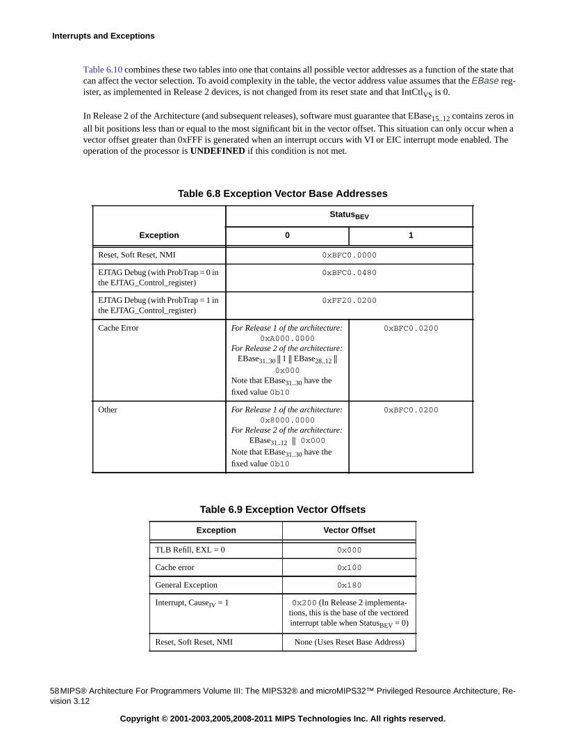
Interrupts and Exceptions
58MIPS® Architecture For Programmers Volume III: The MIPS32® and microMIPS32™ Privileged Resource Architecture, Re-vision 3.12
Copyright © 2001-2003,2005,2008-2011 MIPS Technologies Inc. All rights reserved.
Table 6.10 combines these two tables into one that contains all possible vector addresses as a function of the state thatcan affect the vector selection. To avoid complexity in the table, the vector address value assumes that the EBase reg-ister, as implemented in Release 2 devices, is not changed from its reset state and that IntCtlVS is 0.
In Release 2 of the Architecture (and subsequent releases), software must guarantee that EBase15..12 contains zeros inall bit positions less than or equal to the most significant bit in the vector offset. This situation can only occur when avector offset greater than 0xFFF is generated when an interrupt occurs with VI or EIC interrupt mode enabled. Theoperation of the processor is UNDEFINED if this condition is not met.
Table 6.8 Exception Vector Base Addresses
Exception
StatusBEV
0 1
Reset, Soft Reset, NMI 0xBFC0.0000
EJTAG Debug (with ProbTrap = 0 inthe EJTAG_Control_register)
0xBFC0.0480
EJTAG Debug (with ProbTrap = 1 inthe EJTAG_Control_register)
0xFF20.0200
Cache Error For Release 1 of the architecture:0xA000.0000
For Release 2 of the architecture:EBase31..30 || 1 || EBase28..12 ||
0x000Note that EBase31..30 have the
fixed value 0b10
0xBFC0.0200
Other For Release 1 of the architecture:0x8000.0000
For Release 2 of the architecture:EBase31..12 || 0x000
Note that EBase31..30 have the
fixed value 0b10
0xBFC0.0200
Table 6.9 Exception Vector Offsets
Exception Vector Offset
TLB Refill, EXL = 0 0x000
Cache error 0x100
General Exception 0x180
Interrupt, CauseIV = 1 0x200 (In Release 2 implementa-tions, this is the base of the vectoredinterrupt table when StatusBEV = 0)
Reset, Soft Reset, NMI None (Uses Reset Base Address)
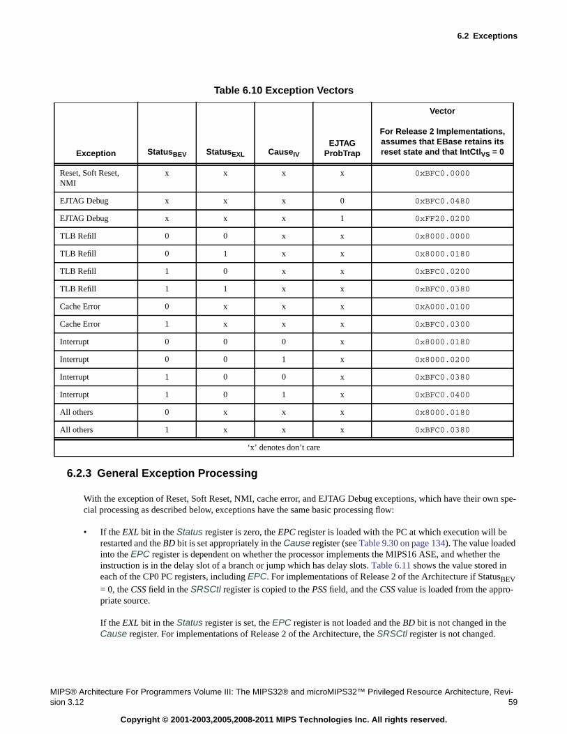
6.2 Exceptions
MIPS® Architecture For Programmers Volume III: The MIPS32® and microMIPS32™ Privileged Resource Architecture, Revi-sion 3.12 59
Copyright © 2001-2003,2005,2008-2011 MIPS Technologies Inc. All rights reserved.
6.2.3 General Exception Processing
With the exception of Reset, Soft Reset, NMI, cache error, and EJTAG Debug exceptions, which have their own spe-cial processing as described below, exceptions have the same basic processing flow:
• If the EXL bit in the Status register is zero, the EPC register is loaded with the PC at which execution will berestarted and the BD bit is set appropriately in the Cause register (see Table 9.30 on page 134). The value loadedinto the EPC register is dependent on whether the processor implements the MIPS16 ASE, and whether theinstruction is in the delay slot of a branch or jump which has delay slots. Table 6.11 shows the value stored ineach of the CP0 PC registers, including EPC. For implementations of Release 2 of the Architecture if StatusBEV
= 0, the CSS field in the SRSCtl register is copied to the PSS field, and the CSS value is loaded from the appro-priate source.
If the EXL bit in the Status register is set, the EPC register is not loaded and the BD bit is not changed in theCause register. For implementations of Release 2 of the Architecture, the SRSCtl register is not changed.
Table 6.10 Exception Vectors
Exception StatusBEV StatusEXL CauseIV
EJTAGProbTrap
Vector
For Release 2 Implementations,assumes that EBase retains itsreset state and that IntCtlVS = 0
Reset, Soft Reset,NMI
x x x x 0xBFC0.0000
EJTAG Debug x x x 0 0xBFC0.0480
EJTAG Debug x x x 1 0xFF20.0200
TLB Refill 0 0 x x 0x8000.0000
TLB Refill 0 1 x x 0x8000.0180
TLB Refill 1 0 x x 0xBFC0.0200
TLB Refill 1 1 x x 0xBFC0.0380
Cache Error 0 x x x 0xA000.0100
Cache Error 1 x x x 0xBFC0.0300
Interrupt 0 0 0 x 0x8000.0180
Interrupt 0 0 1 x 0x8000.0200
Interrupt 1 0 0 x 0xBFC0.0380
Interrupt 1 0 1 x 0xBFC0.0400
All others 0 x x x 0x8000.0180
All others 1 x x x 0xBFC0.0380
‘x’ denotes don’t care
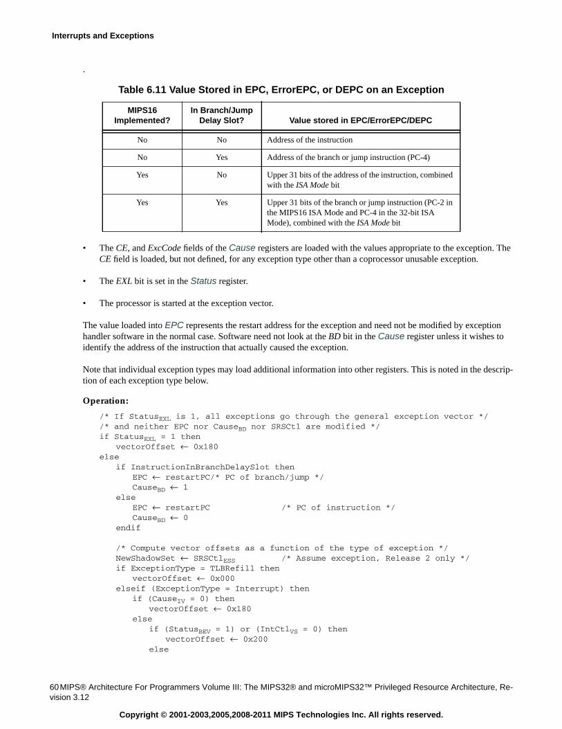
Interrupts and Exceptions
60MIPS® Architecture For Programmers Volume III: The MIPS32® and microMIPS32™ Privileged Resource Architecture, Re-vision 3.12
Copyright © 2001-2003,2005,2008-2011 MIPS Technologies Inc. All rights reserved.
.
• The CE, and ExcCode fields of the Cause registers are loaded with the values appropriate to the exception. TheCE field is loaded, but not defined, for any exception type other than a coprocessor unusable exception.
• The EXL bit is set in the Status register.
• The processor is started at the exception vector.
The value loaded into EPC represents the restart address for the exception and need not be modified by exceptionhandler software in the normal case. Software need not look at the BD bit in the Cause register unless it wishes toidentify the address of the instruction that actually caused the exception.
Note that individual exception types may load additional information into other registers. This is noted in the descrip-tion of each exception type below.
Operation:
/* If StatusEXL is 1, all exceptions go through the general exception vector *//* and neither EPC nor CauseBD nor SRSCtl are modified */if StatusEXL = 1 then
vectorOffset ← 0x180else
if InstructionInBranchDelaySlot thenEPC ← restartPC/* PC of branch/jump */CauseBD ← 1
elseEPC ← restartPC /* PC of instruction */CauseBD ← 0
endif
/* Compute vector offsets as a function of the type of exception */NewShadowSet ← SRSCtlESS /* Assume exception, Release 2 only */if ExceptionType = TLBRefill then
vectorOffset ← 0x000elseif (ExceptionType = Interrupt) then
if (CauseIV = 0) thenvectorOffset ← 0x180
elseif (StatusBEV = 1) or (IntCtlVS = 0) then
vectorOffset ← 0x200else
Table 6.11 Value Stored in EPC, ErrorEPC, or DEPC on an Exception
MIPS16Implemented?
In Branch/JumpDelay Slot? Value stored in EPC/ErrorEPC/DEPC
No No Address of the instruction
No Yes Address of the branch or jump instruction (PC-4)
Yes No Upper 31 bits of the address of the instruction, combinedwith the ISA Mode bit
Yes Yes Upper 31 bits of the branch or jump instruction (PC-2 inthe MIPS16 ISA Mode and PC-4 in the 32-bit ISAMode), combined with the ISA Mode bit
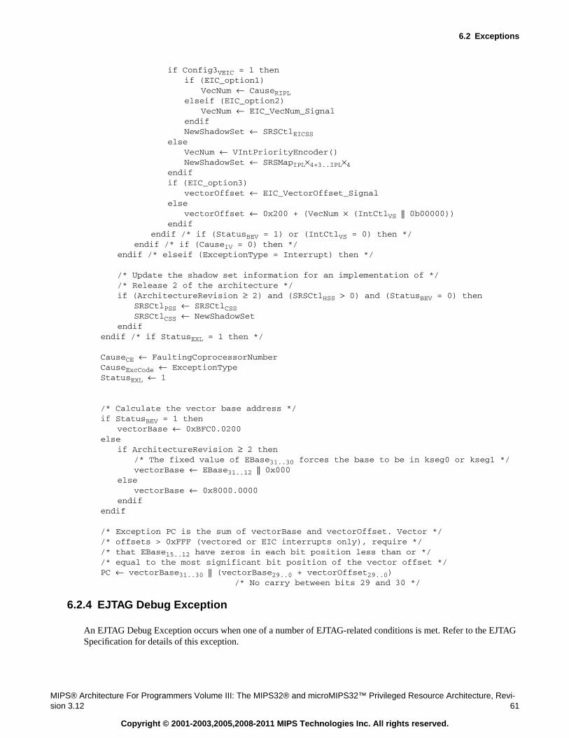
6.2 Exceptions
MIPS® Architecture For Programmers Volume III: The MIPS32® and microMIPS32™ Privileged Resource Architecture, Revi-sion 3.12 61
Copyright © 2001-2003,2005,2008-2011 MIPS Technologies Inc. All rights reserved.
if Config3VEIC = 1 thenif (EIC_option1)
VecNum ← CauseRIPLelseif (EIC_option2)
VecNum ← EIC_VecNum_SignalendifNewShadowSet ← SRSCtlEICSS
elseVecNum ← VIntPriorityEncoder()NewShadowSet ← SRSMapIPL×4+3..IPL×4
endifif (EIC_option3)
vectorOffset ← EIC_VectorOffset_Signalelse
vectorOffset ← 0x200 + (VecNum × (IntCtlVS || 0b00000))endif
endif /* if (StatusBEV = 1) or (IntCtlVS = 0) then */endif /* if (CauseIV = 0) then */
endif /* elseif (ExceptionType = Interrupt) then */
/* Update the shadow set information for an implementation of *//* Release 2 of the architecture */if (ArchitectureRevision ≥ 2) and (SRSCtlHSS > 0) and (StatusBEV = 0) then
SRSCtlPSS ← SRSCtlCSSSRSCtlCSS ← NewShadowSet
endifendif /* if StatusEXL = 1 then */
CauseCE ← FaultingCoprocessorNumberCauseExcCode ← ExceptionTypeStatusEXL ← 1
/* Calculate the vector base address */if StatusBEV = 1 then
vectorBase ← 0xBFC0.0200else
if ArchitectureRevision ≥ 2 then/* The fixed value of EBase31..30 forces the base to be in kseg0 or kseg1 */vectorBase ← EBase31..12 || 0x000
elsevectorBase ← 0x8000.0000
endifendif
/* Exception PC is the sum of vectorBase and vectorOffset. Vector *//* offsets > 0xFFF (vectored or EIC interrupts only), require *//* that EBase15..12 have zeros in each bit position less than or *//* equal to the most significant bit position of the vector offset */PC ← vectorBase31..30 || (vectorBase29..0 + vectorOffset29..0)
/* No carry between bits 29 and 30 */
6.2.4 EJTAG Debug Exception
An EJTAG Debug Exception occurs when one of a number of EJTAG-related conditions is met. Refer to the EJTAGSpecification for details of this exception.
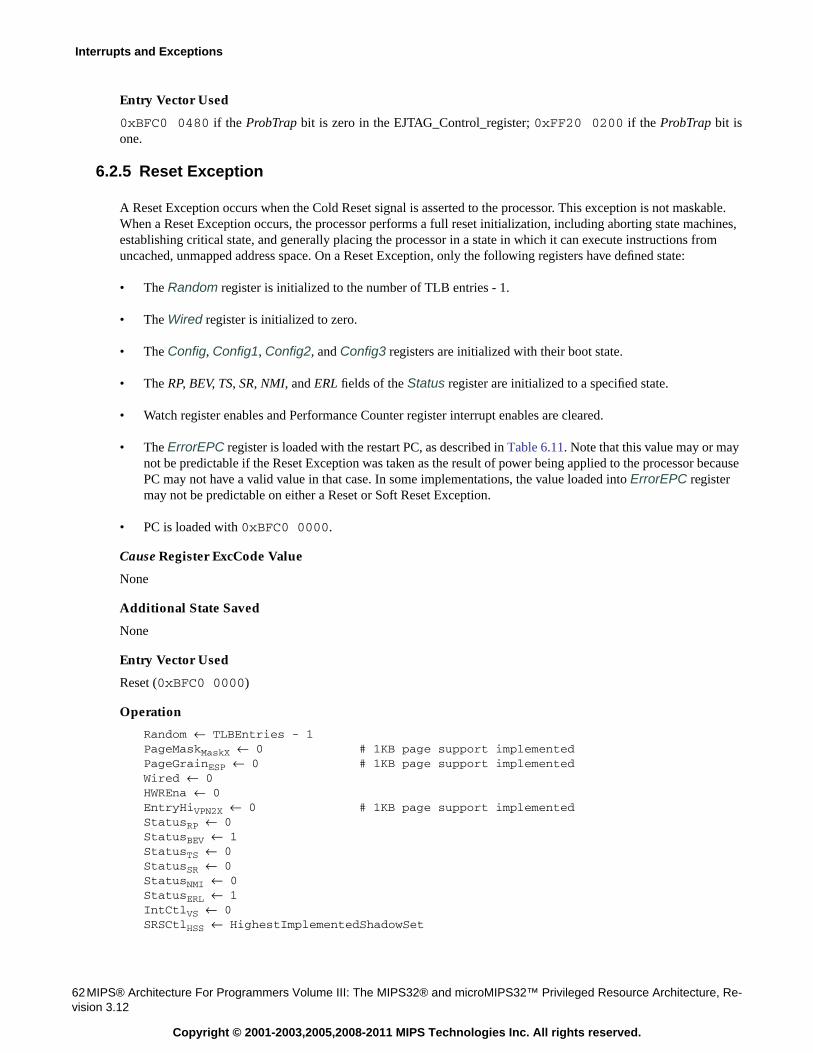
Interrupts and Exceptions
62MIPS® Architecture For Programmers Volume III: The MIPS32® and microMIPS32™ Privileged Resource Architecture, Re-vision 3.12
Copyright © 2001-2003,2005,2008-2011 MIPS Technologies Inc. All rights reserved.
Entry Vector Used
0xBFC0 0480 if the ProbTrap bit is zero in the EJTAG_Control_register; 0xFF20 0200 if the ProbTrap bit isone.
6.2.5 Reset Exception
A Reset Exception occurs when the Cold Reset signal is asserted to the processor. This exception is not maskable.When a Reset Exception occurs, the processor performs a full reset initialization, including aborting state machines,establishing critical state, and generally placing the processor in a state in which it can execute instructions fromuncached, unmapped address space. On a Reset Exception, only the following registers have defined state:
• The Random register is initialized to the number of TLB entries - 1.
• The Wired register is initialized to zero.
• The Config, Config1, Config2, and Config3 registers are initialized with their boot state.
• The RP, BEV, TS, SR, NMI, and ERL fields of the Status register are initialized to a specified state.
• Watch register enables and Performance Counter register interrupt enables are cleared.
• The ErrorEPC register is loaded with the restart PC, as described in Table 6.11. Note that this value may or maynot be predictable if the Reset Exception was taken as the result of power being applied to the processor becausePC may not have a valid value in that case. In some implementations, the value loaded into ErrorEPC registermay not be predictable on either a Reset or Soft Reset Exception.
• PC is loaded with 0xBFC0 0000.
Cause Register ExcCode Value
None
Additional State Saved
None
Entry Vector Used
Reset (0xBFC0 0000)
Operation
Random ← TLBEntries - 1PageMaskMaskX ← 0 # 1KB page support implementedPageGrainESP ← 0 # 1KB page support implementedWired ← 0HWREna ← 0EntryHiVPN2X ← 0 # 1KB page support implementedStatusRP ← 0StatusBEV ← 1StatusTS ← 0StatusSR ← 0StatusNMI ← 0StatusERL ← 1IntCtlVS ← 0SRSCtlHSS ← HighestImplementedShadowSet
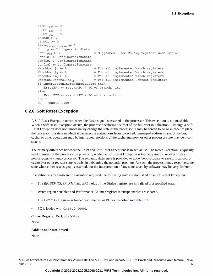
6.2 Exceptions
MIPS® Architecture For Programmers Volume III: The MIPS32® and microMIPS32™ Privileged Resource Architecture, Revi-sion 3.12 63
Copyright © 2001-2003,2005,2008-2011 MIPS Technologies Inc. All rights reserved.
SRSCtlESS ← 0SRSCtlPSS ← 0SRSCtlCSS ← 0SRSMap ← 0CauseDC ← 0EBaseExceptionBase ← 0Config ← ConfigurationStateConfigK0 ← 2 # Suggested - see Config register descriptionConfig1 ← ConfigurationStateConfig2 ← ConfigurationStateConfig3 ← ConfigurationStateWatchLo[n]I ← 0 # For all implemented Watch registersWatchLo[n]R ← 0 # For all implemented Watch registersWatchLo[n]W ← 0 # For all implemented Watch registersPerfCnt.Control[n]IE ← 0 # For all implemented PerfCnt registersif InstructionInBranchDelaySlot then
ErrorEPC ← restartPC # PC of branch/jumpelse
ErrorEPC ← restartPC # PC of instructionendifPC ← 0xBFC0 0000
6.2.6 Soft Reset Exception
A Soft Reset Exception occurs when the Reset signal is asserted to the processor. This exception is not maskable.When a Soft Reset Exception occurs, the processor performs a subset of the full reset initialization. Although a SoftReset Exception does not unnecessarily change the state of the processor, it may be forced to do so in order to placethe processor in a state in which it can execute instructions from uncached, unmapped address space. Since bus,cache, or other operations may be interrupted, portions of the cache, memory, or other processor state may be incon-sistent.
The primary difference between the Reset and Soft Reset Exceptions is in actual use. The Reset Exception is typicallyused to initialize the processor on power-up, while the Soft Reset Exception is typically used to recover from anon-responsive (hung) processor. The semantic difference is provided to allow boot software to save critical copro-cessor 0 or other register state to assist in debugging the potential problem. As such, the processor may reset the samestate when either reset signal is asserted, but the interpretation of any state saved by software may be very different.
In addition to any hardware initialization required, the following state is established on a Soft Reset Exception:
• The RP, BEV, TS, SR, NMI, and ERL fields of the Status register are initialized to a specified state.
• Watch register enables and Performance Counter register interrupt enables are cleared.
• The ErrorEPC register is loaded with the restart PC, as described in Table 6.11.
• PC is loaded with 0xBFC0 0000.
Cause Register ExcCode Value
None
Additional State Saved
None
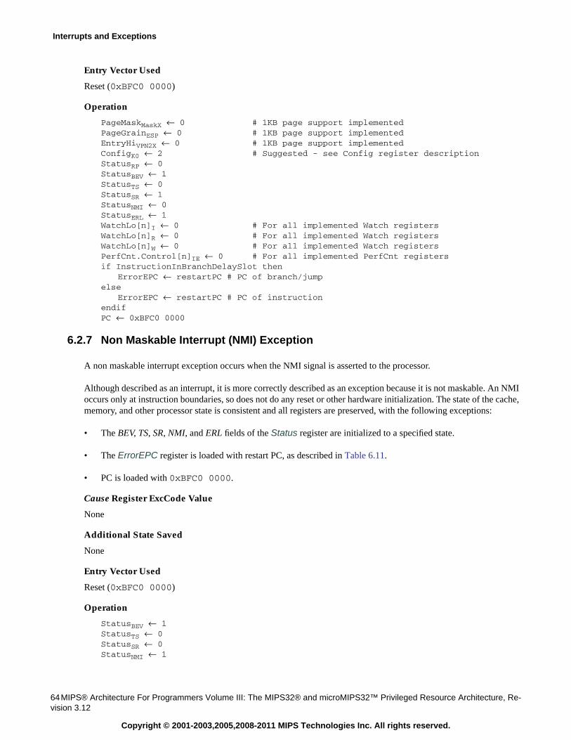
Interrupts and Exceptions
64MIPS® Architecture For Programmers Volume III: The MIPS32® and microMIPS32™ Privileged Resource Architecture, Re-vision 3.12
Copyright © 2001-2003,2005,2008-2011 MIPS Technologies Inc. All rights reserved.
Entry Vector Used
Reset (0xBFC0 0000)
Operation
PageMaskMaskX ← 0 # 1KB page support implementedPageGrainESP ← 0 # 1KB page support implementedEntryHiVPN2X ← 0 # 1KB page support implementedConfigK0 ← 2 # Suggested - see Config register descriptionStatusRP ← 0StatusBEV ← 1StatusTS ← 0StatusSR ← 1StatusNMI ← 0StatusERL ← 1WatchLo[n]I ← 0 # For all implemented Watch registersWatchLo[n]R ← 0 # For all implemented Watch registersWatchLo[n]W ← 0 # For all implemented Watch registersPerfCnt.Control[n]IE ← 0 # For all implemented PerfCnt registersif InstructionInBranchDelaySlot then
ErrorEPC ← restartPC # PC of branch/jumpelse
ErrorEPC ← restartPC # PC of instructionendifPC ← 0xBFC0 0000
6.2.7 Non Maskable Interrupt (NMI) Exception
A non maskable interrupt exception occurs when the NMI signal is asserted to the processor.
Although described as an interrupt, it is more correctly described as an exception because it is not maskable. An NMIoccurs only at instruction boundaries, so does not do any reset or other hardware initialization. The state of the cache,memory, and other processor state is consistent and all registers are preserved, with the following exceptions:
• The BEV, TS, SR, NMI, and ERL fields of the Status register are initialized to a specified state.
• The ErrorEPC register is loaded with restart PC, as described in Table 6.11.
• PC is loaded with 0xBFC0 0000.
Cause Register ExcCode Value
None
Additional State Saved
None
Entry Vector Used
Reset (0xBFC0 0000)
Operation
StatusBEV ← 1StatusTS ← 0StatusSR ← 0StatusNMI ← 1
6.2 Exceptions
MIPS® Architecture For Programmers Volume III: The MIPS32® and microMIPS32™ Privileged Resource Architecture, Revi-sion 3.12 65
Copyright © 2001-2003,2005,2008-2011 MIPS Technologies Inc. All rights reserved.
StatusERL ← 1if InstructionInBranchDelaySlot then
ErrorEPC ← restartPC # PC of branch/jumpelse
ErrorEPC ← restartPC # PC of instructionendifPC ← 0xBFC0 0000
6.2.8 Machine Check Exception
A machine check exception occurs when the processor detects an internal inconsistency.
The following conditions cause a machine check exception:
• Detection of multiple matching entries in the TLB in a TLB-based MMU.
Cause Register ExcCode Value
MCheck (See Table 9.31 on page 138)
Additional State Saved
Depends on the condition that caused the exception. See the descriptions above.
Entry Vector Used
General exception vector (offset 0x180)
6.2.9 Address Error Exception
An address error exception occurs under the following circumstances:
• An instruction is fetched from an address that is not aligned on a word boundary.
• A load or store word instruction is executed in which the address is not aligned on a word boundary.
• A load or store halfword instruction is executed in which the address is not aligned on a halfword boundary.
• A reference is made to a kernel address space from User Mode or Supervisor Mode.
• A reference is made to a supervisor address space from User Mode.
Note that in the case of an instruction fetch that is not aligned on a word boundary, the PC is updated before the con-dition is detected. Therefore, both EPC and BadVAddr point at the unaligned instruction address.
Cause Register ExcCode Value
AdEL: Reference was a load or an instruction fetch
AdES: Reference was a store
See Table 9.31 on page 138.
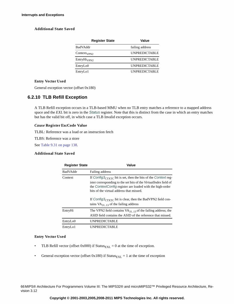
Interrupts and Exceptions
66MIPS® Architecture For Programmers Volume III: The MIPS32® and microMIPS32™ Privileged Resource Architecture, Re-vision 3.12
Copyright © 2001-2003,2005,2008-2011 MIPS Technologies Inc. All rights reserved.
Additional State Saved
Entry Vector Used
General exception vector (offset 0x180)
6.2.10 TLB Refill Exception
A TLB Refill exception occurs in a TLB-based MMU when no TLB entry matches a reference to a mapped addressspace and the EXL bit is zero in the Status register. Note that this is distinct from the case in which an entry matchesbut has the valid bit off, in which case a TLB Invalid exception occurs.
Cause Register ExcCode Value
TLBL: Reference was a load or an instruction fetch
TLBS: Reference was a store
See Table 9.31 on page 138.
Additional State Saved
Entry Vector Used
• TLB Refill vector (offset 0x000) if StatusEXL = 0 at the time of exception.
• General exception vector (offset 0x180) if StatusEXL = 1 at the time of exception
Register State Value
BadVAddr failing address
ContextVPN2 UNPREDICTABLE
EntryHiVPN2 UNPREDICTABLE
EntryLo0 UNPREDICTABLE
EntryLo1 UNPREDICTABLE
Register State Value
BadVAddr Failing address
Context If Config3CTXTC bit is set, then the bits of the Context reg-
ister corresponding to the set bits of the VirtualIndex field ofthe ContextConfig register are loaded with the high-orderbits of the virtual address that missed.
If Config3CTXTC bit is clear, then the BadVPN2 field con-
tains VA31..13 of the failing address
EntryHi The VPN2 field contains VA31..13 of the failing address; the
ASID field contains the ASID of the reference that missed.
EntryLo0 UNPREDICTABLE
EntryLo1 UNPREDICTABLE
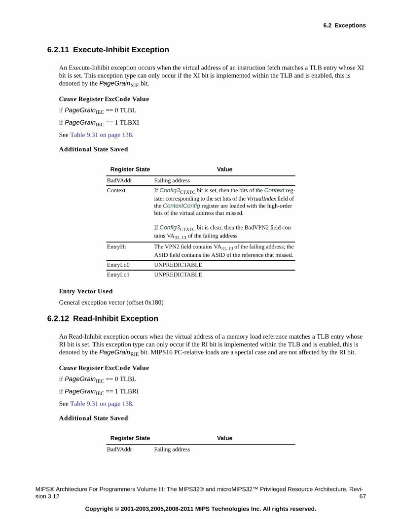
6.2 Exceptions
MIPS® Architecture For Programmers Volume III: The MIPS32® and microMIPS32™ Privileged Resource Architecture, Revi-sion 3.12 67
Copyright © 2001-2003,2005,2008-2011 MIPS Technologies Inc. All rights reserved.
6.2.11 Execute-Inhibit Exception
An Execute-Inhibit exception occurs when the virtual address of an instruction fetch matches a TLB entry whose XIbit is set. This exception type can only occur if the XI bit is implemented within the TLB and is enabled, this isdenoted by the PageGrainXIE bit.
Cause Register ExcCode Value
if PageGrainIEC == 0 TLBL
if PageGrainIEC == 1 TLBXI
See Table 9.31 on page 138.
Additional State Saved
Entry Vector Used
General exception vector (offset 0x180)
6.2.12 Read-Inhibit Exception
An Read-Inhibit exception occurs when the virtual address of a memory load reference matches a TLB entry whoseRI bit is set. This exception type can only occur if the RI bit is implemented within the TLB and is enabled, this isdenoted by the PageGrainRIE bit. MIPS16 PC-relative loads are a special case and are not affected by the RI bit.
Cause Register ExcCode Value
if PageGrainIEC == 0 TLBL
if PageGrainIEC == 1 TLBRI
See Table 9.31 on page 138.
Additional State Saved
Register State Value
BadVAddr Failing address
Context If Config3CTXTC bit is set, then the bits of the Context reg-
ister corresponding to the set bits of the VirtualIndex field ofthe ContextConfig register are loaded with the high-orderbits of the virtual address that missed.
If Config3CTXTC bit is clear, then the BadVPN2 field con-
tains VA31..13 of the failing address
EntryHi The VPN2 field contains VA31..13 of the failing address; the
ASID field contains the ASID of the reference that missed.
EntryLo0 UNPREDICTABLE
EntryLo1 UNPREDICTABLE
Register State Value
BadVAddr Failing address
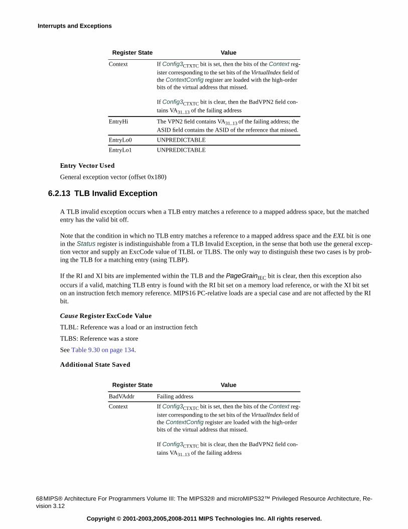
Interrupts and Exceptions
68MIPS® Architecture For Programmers Volume III: The MIPS32® and microMIPS32™ Privileged Resource Architecture, Re-vision 3.12
Copyright © 2001-2003,2005,2008-2011 MIPS Technologies Inc. All rights reserved.
Entry Vector Used
General exception vector (offset 0x180)
6.2.13 TLB Invalid Exception
A TLB invalid exception occurs when a TLB entry matches a reference to a mapped address space, but the matchedentry has the valid bit off.
Note that the condition in which no TLB entry matches a reference to a mapped address space and the EXL bit is onein the Status register is indistinguishable from a TLB Invalid Exception, in the sense that both use the general excep-tion vector and supply an ExcCode value of TLBL or TLBS. The only way to distinguish these two cases is by prob-ing the TLB for a matching entry (using TLBP).
If the RI and XI bits are implemented within the TLB and the PageGrainIEC bit is clear, then this exception alsooccurs if a valid, matching TLB entry is found with the RI bit set on a memory load reference, or with the XI bit seton an instruction fetch memory reference. MIPS16 PC-relative loads are a special case and are not affected by the RIbit.
Cause Register ExcCode Value
TLBL: Reference was a load or an instruction fetch
TLBS: Reference was a store
See Table 9.30 on page 134.
Additional State Saved
Context If Config3CTXTC bit is set, then the bits of the Context reg-
ister corresponding to the set bits of the VirtualIndex field ofthe ContextConfig register are loaded with the high-orderbits of the virtual address that missed.
If Config3CTXTC bit is clear, then the BadVPN2 field con-
tains VA31..13 of the failing address
EntryHi The VPN2 field contains VA31..13 of the failing address; the
ASID field contains the ASID of the reference that missed.
EntryLo0 UNPREDICTABLE
EntryLo1 UNPREDICTABLE
Register State Value
BadVAddr Failing address
Context If Config3CTXTC bit is set, then the bits of the Context reg-
ister corresponding to the set bits of the VirtualIndex field ofthe ContextConfig register are loaded with the high-orderbits of the virtual address that missed.
If Config3CTXTC bit is clear, then the BadVPN2 field con-
tains VA31..13 of the failing address
Register State Value
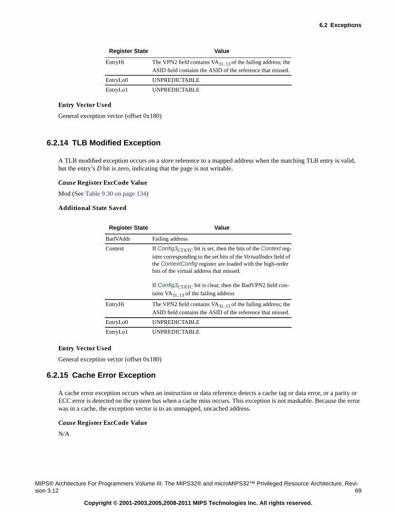
6.2 Exceptions
MIPS® Architecture For Programmers Volume III: The MIPS32® and microMIPS32™ Privileged Resource Architecture, Revi-sion 3.12 69
Copyright © 2001-2003,2005,2008-2011 MIPS Technologies Inc. All rights reserved.
Entry Vector Used
General exception vector (offset 0x180)
6.2.14 TLB Modified Exception
A TLB modified exception occurs on a store reference to a mapped address when the matching TLB entry is valid,but the entry’s D bit is zero, indicating that the page is not writable.
Cause Register ExcCode Value
Mod (See Table 9.30 on page 134)
Additional State Saved
Entry Vector Used
General exception vector (offset 0x180)
6.2.15 Cache Error Exception
A cache error exception occurs when an instruction or data reference detects a cache tag or data error, or a parity orECC error is detected on the system bus when a cache miss occurs. This exception is not maskable. Because the errorwas in a cache, the exception vector is to an unmapped, uncached address.
Cause Register ExcCode Value
N/A
EntryHi The VPN2 field contains VA31..13 of the failing address; the
ASID field contains the ASID of the reference that missed.
EntryLo0 UNPREDICTABLE
EntryLo1 UNPREDICTABLE
Register State Value
BadVAddr Failing address
Context If Config3CTXTC bit is set, then the bits of the Context reg-
ister corresponding to the set bits of the VirtualIndex field ofthe ContextConfig register are loaded with the high-orderbits of the virtual address that missed.
If Config3CTXTC bit is clear, then the BadVPN2 field con-
tains VA31..13 of the failing address
EntryHi The VPN2 field contains VA31..13 of the failing address; the
ASID field contains the ASID of the reference that missed.
EntryLo0 UNPREDICTABLE
EntryLo1 UNPREDICTABLE
Register State Value
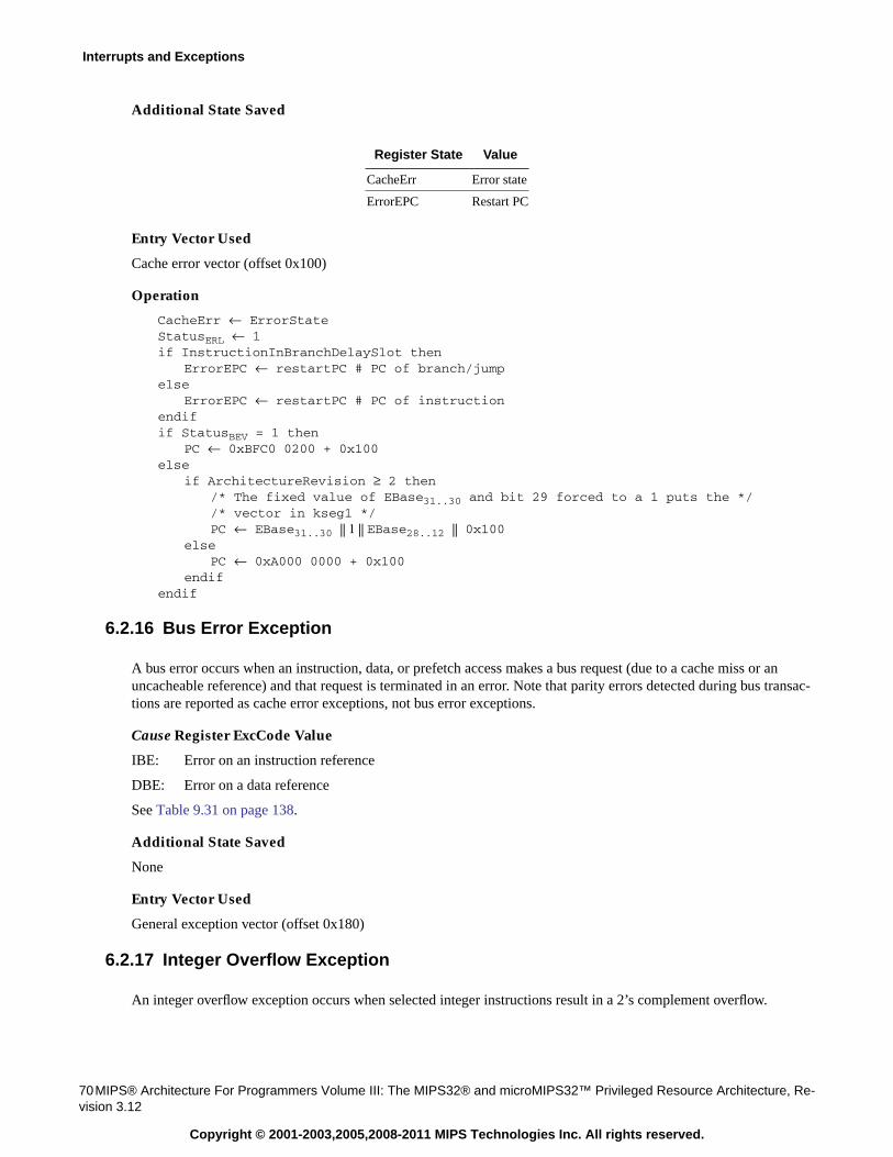
Interrupts and Exceptions
70MIPS® Architecture For Programmers Volume III: The MIPS32® and microMIPS32™ Privileged Resource Architecture, Re-vision 3.12
Copyright © 2001-2003,2005,2008-2011 MIPS Technologies Inc. All rights reserved.
Additional State Saved
Entry Vector Used
Cache error vector (offset 0x100)
Operation
CacheErr ← ErrorStateStatusERL ← 1if InstructionInBranchDelaySlot then
ErrorEPC ← restartPC # PC of branch/jumpelse
ErrorEPC ← restartPC # PC of instructionendifif StatusBEV = 1 then
PC ← 0xBFC0 0200 + 0x100else
if ArchitectureRevision ≥ 2 then/* The fixed value of EBase31..30 and bit 29 forced to a 1 puts the *//* vector in kseg1 */PC ← EBase31..30 || 1 || EBase28..12 || 0x100
elsePC ← 0xA000 0000 + 0x100
endifendif
6.2.16 Bus Error Exception
A bus error occurs when an instruction, data, or prefetch access makes a bus request (due to a cache miss or anuncacheable reference) and that request is terminated in an error. Note that parity errors detected during bus transac-tions are reported as cache error exceptions, not bus error exceptions.
Cause Register ExcCode Value
IBE: Error on an instruction reference
DBE: Error on a data reference
See Table 9.31 on page 138.
Additional State Saved
None
Entry Vector Used
General exception vector (offset 0x180)
6.2.17 Integer Overflow Exception
An integer overflow exception occurs when selected integer instructions result in a 2’s complement overflow.
Register State Value
CacheErr Error state
ErrorEPC Restart PC
6.2 Exceptions
MIPS® Architecture For Programmers Volume III: The MIPS32® and microMIPS32™ Privileged Resource Architecture, Revi-sion 3.12 71
Copyright © 2001-2003,2005,2008-2011 MIPS Technologies Inc. All rights reserved.
Cause Register ExcCode Value
Ov (See Table 9.31 on page 138)
Additional State Saved
None
Entry Vector Used
General exception vector (offset 0x180)
6.2.18 Trap Exception
A trap exception occurs when a trap instruction results in a TRUE value.
Cause Register ExcCode Value
Tr (See Table 9.31 on page 138)
Additional State Saved
None
Entry Vector Used
General exception vector (offset 0x180)
6.2.19 System Call Exception
A system call exception occurs when a SYSCALL instruction is executed.
Cause Register ExcCode Value
Sys (See Table 9.30 on page 134)
Additional State Saved
None
Entry Vector Used
General exception vector (offset 0x180)
6.2.20 Breakpoint Exception
A breakpoint exception occurs when a BREAK instruction is executed.
Cause Register ExcCode Value
Bp (See Table 9.31 on page 138)
Additional State Saved
None
Entry Vector Used
General exception vector (offset 0x180)
Interrupts and Exceptions
72MIPS® Architecture For Programmers Volume III: The MIPS32® and microMIPS32™ Privileged Resource Architecture, Re-vision 3.12
Copyright © 2001-2003,2005,2008-2011 MIPS Technologies Inc. All rights reserved.
6.2.21 Reserved Instruction Exception
A Reserved Instruction Exception occurs if any of the following conditions is true:
• An instruction was executed that specifies an encoding of the opcode field that is flagged with “∗” (reserved),“β” (higher-order ISA), or an unimplemented “ε” (ASE).
• An instruction was executed that specifies a SPECIAL opcode encoding of the function field that is flagged with“∗” (reserved), or “β” (higher-order ISA).
• An instruction was executed that specifies a REGIMM opcode encoding of the rt field that is flagged with “∗”(reserved).
• An instruction was executed that specifies an unimplemented SPECIAL2 opcode encoding of the function fieldthat is flagged with an unimplemented “θ” (partner available), or an unimplemented “σ” (EJTAG).
• An instruction was executed that specifies a COPz opcode encoding of the rs field that is flagged with “∗”(reserved), “β” (higher-order ISA), or an unimplemented “ε” (ASE), assuming that access to the coprocessor isallowed. If access to the coprocessor is not allowed, a Coprocessor Unusable Exception occurs instead. For theCOP1 opcode, some implementations of previous ISAs reported this case as a Floating Point Exception, settingthe Unimplemented Operation bit in the Cause field of the FCSR register.
• An instruction was executed that specifies an unimplemented COP0 opcode encoding of the function field whenrs is CO that is flagged with “∗” (reserved), or an unimplemented “σ” (EJTAG), assuming that access to copro-cessor 0 is allowed. If access to the coprocessor is not allowed, a Coprocessor Unusable Exception occursinstead.
• An instruction was executed that specifies a COP1 opcode encoding of the function field that is flagged with “∗”(reserved), “β” (higher-order ISA), or an unimplemented “ε” (ASE), assuming that access to coprocessor 1 isallowed. If access to the coprocessor is not allowed, a Coprocessor Unusable Exception occurs instead. Someimplementations of previous ISAs reported this case as a Floating Point Exception, setting the UnimplementedOperation bit in the Cause field of the FCSR register.
Cause Register ExcCode Value
RI (See Table 9.31 on page 138)
Additional State Saved
None
Entry Vector Used
General exception vector (offset 0x180)
6.2.22 Coprocessor Unusable Exception
A coprocessor unusable exception occurs if any of the following conditions is true:
• A COP0 or Cache instruction was executed while the processor was running in a mode other than Debug Modeor Kernel Mode, and the CU0 bit in the Status register was a zero
• A COP1, COP1X,LWC1, SWC1, LDC1, SDC1 or MOVCI (Special opcode function field encoding) instructionwas executed and the CU1 bit in the Status register was a zero.
6.2 Exceptions
MIPS® Architecture For Programmers Volume III: The MIPS32® and microMIPS32™ Privileged Resource Architecture, Revi-sion 3.12 73
Copyright © 2001-2003,2005,2008-2011 MIPS Technologies Inc. All rights reserved.
• A COP2, LWC2, SWC2, LDC2, or SDC2 instruction was executed, and the CU2 bit in the Status register was azero. COP2 instructions include MFC2, DMFC2, CFC2, MFHC2, MTC2, DMTC2, CTC2, MTHC2.
NOTE: In Release 2 of the MIPS32 Architecture, the use of COP3 as a user-defined coprocessor has been removed.The use of COP3 is reserved for the future extension of the architecture.
Cause Register ExcCode Value
CpU (See Table 9.30 on page 134)
Additional State Saved
Entry Vector Used
General exception vector (offset 0x180)
6.2.23 Floating Point Exception
A floating point exception is initiated by the floating point coprocessor to signal a floating point exception.
Register ExcCode Value
FPE (See Table 9.30 on page 134)
Additional State Saved
Entry Vector Used
General exception vector (offset 0x180)
6.2.24 Coprocessor 2 Exception
A coprocessor 2 exception is initiated by coprocessor 2 to signal a precise coprocessor 2 exception.
Register ExcCode Value
C2E (See Table 9.30 on page 134)
Additional State Saved
Defined by the coprocessor
Entry Vector Used
General exception vector (offset 0x180)
Register State Value
CauseCE unit number of the coprocessor being referenced
Register State Value
FCSR indicates the cause of the floating point exception
Interrupts and Exceptions
74MIPS® Architecture For Programmers Volume III: The MIPS32® and microMIPS32™ Privileged Resource Architecture, Re-vision 3.12
Copyright © 2001-2003,2005,2008-2011 MIPS Technologies Inc. All rights reserved.
6.2.25 Watch Exception
The watch facility provides a software debugging vehicle by initiating a watch exception when an instruction or datareference matches the address information stored in the WatchHi and WatchLo registers. A watch exception is takenimmediately if the EXL and ERL bits of the Status register are both zero. If either bit is a one at the time that a watchexception would normally be taken, the WP bit in the Cause register is set, and the exception is deferred until boththe EXL and ERL bits in the Status register are zero. Software may use the WP bit in the Cause register to determineif the EPC register points at the instruction that caused the watch exception, or if the exception actually occurredwhile in kernel mode.
If the EXL or ERL bits are one in the Status register and a single instruction generates both a watch exception (whichis deferred by the state of the EXL and ERL bits) and a lower-priority exception, the lower priority exception is taken.
Watch exceptions are never taken if the processor is executing in Debug Mode. Should a watch register match whilethe processor is in Debug Mode, the exception is inhibited and the WP bit is not changed.
It is implementation dependent whether a data watch exception is triggered by a prefetch or cache instruction whoseaddress matches the Watch register address match conditions. A watch triggered by a SC instruction does so even ifthe store would not complete because the LL bit is zero.
Register ExcCode Value
WATCH (See Table 9.30 on page 134)
Additional State Saved
Entry Vector Used
General exception vector (offset 0x180)
6.2.26 Interrupt Exception
The interrupt exception occurs when an enabled request for interrupt service is made. See Section 6.1 on page 43 formore information.
Register ExcCode Value
Int (See Table 9.31 on page 138)
Additional State Saved
Register State Value
CauseWP indicates that the watch exception was deferred until afterboth StatusEXL and StatusERL were zero. This bit directly
causes a watch exception, so software must clear this bit aspart of the exception handler to prevent a watch exceptionloop at the end of the current handler execution.
Register State Value
CauseIP indicates the interrupts that are pending.
6.2 Exceptions
MIPS® Architecture For Programmers Volume III: The MIPS32® and microMIPS32™ Privileged Resource Architecture, Revi-sion 3.12 75
Copyright © 2001-2003,2005,2008-2011 MIPS Technologies Inc. All rights reserved.
Entry Vector Used
General exception vector (offset 0x180) if the IV bit in the Cause register is zero.
Interrupt vector (offset 0x200) if the IV bit in the Cause register is one.

Interrupts and Exceptions
76MIPS® Architecture For Programmers Volume III: The MIPS32® and microMIPS32™ Privileged Resource Architecture, Re-vision 3.12
Copyright © 2001-2003,2005,2008-2011 MIPS Technologies Inc. All rights reserved.
Chapter 7
MIPS® Architecture For Programmers Volume III: The MIPS32® and microMIPS32™ Privileged Resource Architecture, Revi-sion 3.12 77
Copyright © 2001-2003,2005,2008-2011 MIPS Technologies Inc. All rights reserved.
GPR Shadow Registers
The capability in this chapter is targeted at removing the need to save and restore GPRs on entry to high priority inter-rupts or exceptions, and to provide specified processor modes with the same capability. This is done by introducingmultiple copies of the GPRs, called shadow sets, and allowing privileged software to associate a shadow set withentry to Kernel Mode via an interrupt vector or exception. The normal GPRs are logically considered shadow setzero.
The number of GPR shadow sets is implementation dependent and may range from one (the normal GPRs) to anarchitectural maximum of 16. The highest number actually implemented is indicated by the SRSCtlHSS field, and allshadow sets between 0 and SRSCtlHSS, inclusive must be implemented. If this field is zero, only the normal GPRs areimplemented.
7.1 Introduction to Shadow Sets
Shadow sets are new copies of the GPRs that can be substituted for the normal GPRs on entry to Kernel Mode via aninterrupt or exception. Once a shadow set is bound to a Kernel Mode entry condition, reference to GPRs work exactlyas one would expect, but they are redirected to registers that are dedicated to that condition. Privileged software mayneed to reference all GPRs in the register file, even specific shadow registers that are not visible in the current mode.The RDPGPR and WRPGPR instructions are used for this purpose. The CSS field of the SRSCtl register providesthe number of the current shadow register set, and the PSS field of the SRSCtl register provides the number of theprevious shadow register set (that which was current before the last exception or interrupt occurred).
If the processor is operating in VI interrupt mode, binding of a vectored interrupt to a shadow set is done by writing tothe SRSMap register. If the processor is operating in EIC interrupt mode, the binding of the interrupt to a specificshadow set is provided by the external interrupt controller, and is configured in an implementation-dependent way.Binding of an exception or non-vectored interrupt to a shadow set is done by writing to the ESS field of the SRSCtlregister. When an exception or interrupt occurs, the value of SRSCtlCSS is copied to SRSCtlPSS, and SRSCtlCSS is setto the value taken from the appropriate source. On an ERET, the value of SRSCtlPSS is copied back into SRSCtlCSS torestore the shadow set of the mode to which control returns. More precisely, the rules for updating the fields in theSRSCtl register on an interrupt or exception are as follows:
1. No field in the SRSCtl register is updated if any of the following conditions are true. In this case, steps 2 and 3are skipped.
• The exception is one that sets StatusERL: NMI or cache error.
• The exception causes entry into EJTAG Debug Mode
• StatusBEV = 1
• StatusEXL = 1
2. SRSCtlCSS is copied to SRSCtlPSS
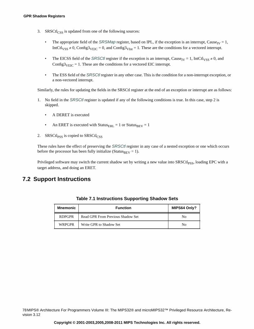
GPR Shadow Registers
78MIPS® Architecture For Programmers Volume III: The MIPS32® and microMIPS32™ Privileged Resource Architecture, Re-vision 3.12
Copyright © 2001-2003,2005,2008-2011 MIPS Technologies Inc. All rights reserved.
3. SRSCtlCSS is updated from one of the following sources:
• The appropriate field of the SRSMap register, based on IPL, if the exception is an interrupt, CauseIV = 1,IntCtlVSS ≠ 0, Config3VEIC = 0, and Config3VInt = 1. These are the conditions for a vectored interrupt.
• The EICSS field of the SRSCtl register if the exception is an interrupt, CauseIV = 1, IntCtlVSS ≠ 0, andConfig3VEIC = 1. These are the conditions for a vectored EIC interrupt.
• The ESS field of the SRSCtl register in any other case. This is the condition for a non-interrupt exception, ora non-vectored interrupt.
Similarly, the rules for updating the fields in the SRSCtl register at the end of an exception or interrupt are as follows:
1. No field in the SRSCtl register is updated if any of the following conditions is true. In this case, step 2 isskipped.
• A DERET is executed
• An ERET is executed with StatusERL = 1 or StatusBEV = 1
2. SRSCtlPSS is copied to SRSCtlCSS
These rules have the effect of preserving the SRSCtl register in any case of a nested exception or one which occursbefore the processor has been fully initialize (StatusBEV = 1).
Privileged software may switch the current shadow set by writing a new value into SRSCtlPSS, loading EPC with atarget address, and doing an ERET.
7.2 Support Instructions
Table 7.1 Instructions Supporting Shadow Sets
Mnemonic Function MIPS64 Only?
RDPGPR Read GPR From Previous Shadow Set No
WRPGPR Write GPR to Shadow Set No
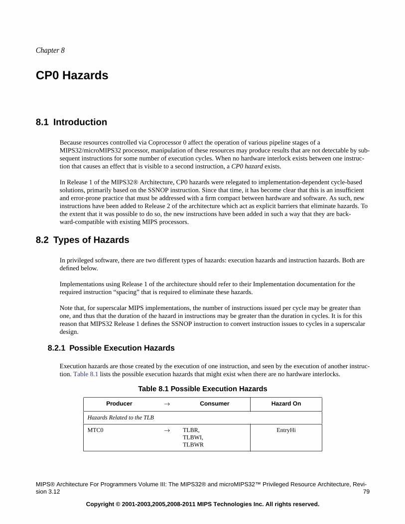
Chapter 8
MIPS® Architecture For Programmers Volume III: The MIPS32® and microMIPS32™ Privileged Resource Architecture, Revi-sion 3.12 79
Copyright © 2001-2003,2005,2008-2011 MIPS Technologies Inc. All rights reserved.
CP0 Hazards
8.1 Introduction
Because resources controlled via Coprocessor 0 affect the operation of various pipeline stages of aMIPS32/microMIPS32 processor, manipulation of these resources may produce results that are not detectable by sub-sequent instructions for some number of execution cycles. When no hardware interlock exists between one instruc-tion that causes an effect that is visible to a second instruction, a CP0 hazard exists.
In Release 1 of the MIPS32® Architecture, CP0 hazards were relegated to implementation-dependent cycle-basedsolutions, primarily based on the SSNOP instruction. Since that time, it has become clear that this is an insufficientand error-prone practice that must be addressed with a firm compact between hardware and software. As such, newinstructions have been added to Release 2 of the architecture which act as explicit barriers that eliminate hazards. Tothe extent that it was possible to do so, the new instructions have been added in such a way that they are back-ward-compatible with existing MIPS processors.
8.2 Types of Hazards
In privileged software, there are two different types of hazards: execution hazards and instruction hazards. Both aredefined below.
Implementations using Release 1 of the architecture should refer to their Implementation documentation for therequired instruction “spacing” that is required to eliminate these hazards.
Note that, for superscalar MIPS implementations, the number of instructions issued per cycle may be greater thanone, and thus that the duration of the hazard in instructions may be greater than the duration in cycles. It is for thisreason that MIPS32 Release 1 defines the SSNOP instruction to convert instruction issues to cycles in a superscalardesign.
8.2.1 Possible Execution Hazards
Execution hazards are those created by the execution of one instruction, and seen by the execution of another instruc-tion. Table 8.1 lists the possible execution hazards that might exist when there are no hardware interlocks.
Table 8.1 Possible Execution Hazards
Producer → Consumer Hazard On
Hazards Related to the TLB
MTC0 → TLBR,TLBWI,TLBWR
EntryHi
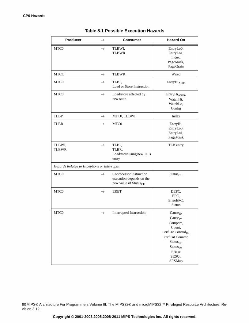
CP0 Hazards
80MIPS® Architecture For Programmers Volume III: The MIPS32® and microMIPS32™ Privileged Resource Architecture, Re-vision 3.12
Copyright © 2001-2003,2005,2008-2011 MIPS Technologies Inc. All rights reserved.
MTC0 → TLBWI,TLBWR
EntryLo0,EntryLo1,
Index,PageMask,PageGrain
MTCO → TLBWR Wired
MTC0 → TLBP,Load or Store Instruction
EntryHiASID
MTC0 → Load/store affected bynew state
EntryHiASID,
WatchHi,WatchLo,
Config
TLBP → MFC0, TLBWI Index
TLBR → MFC0 EntryHi,EntryLo0,EntryLo1,PageMask
TLBWI,TLBWR
→ TLBP,TLBR,Load/store using new TLBentry
TLB entry
Hazards Related to Exceptions or Interrupts
MTC0 → Coprocessor instructionexecution depends on thenew value of StatusCU
StatusCU
MTC0 → ERET DEPC,EPC,
ErrorEPC,Status
MTC0 → Interrupted Instruction CauseIP,
CauseIV
Compare,Count,
PerfCnt ControlIE,
PerfCnt Counter,StatusIE,
StatusIM
EBaseSRSCtl
SRSMap
Table 8.1 Possible Execution Hazards
Producer → Consumer Hazard On
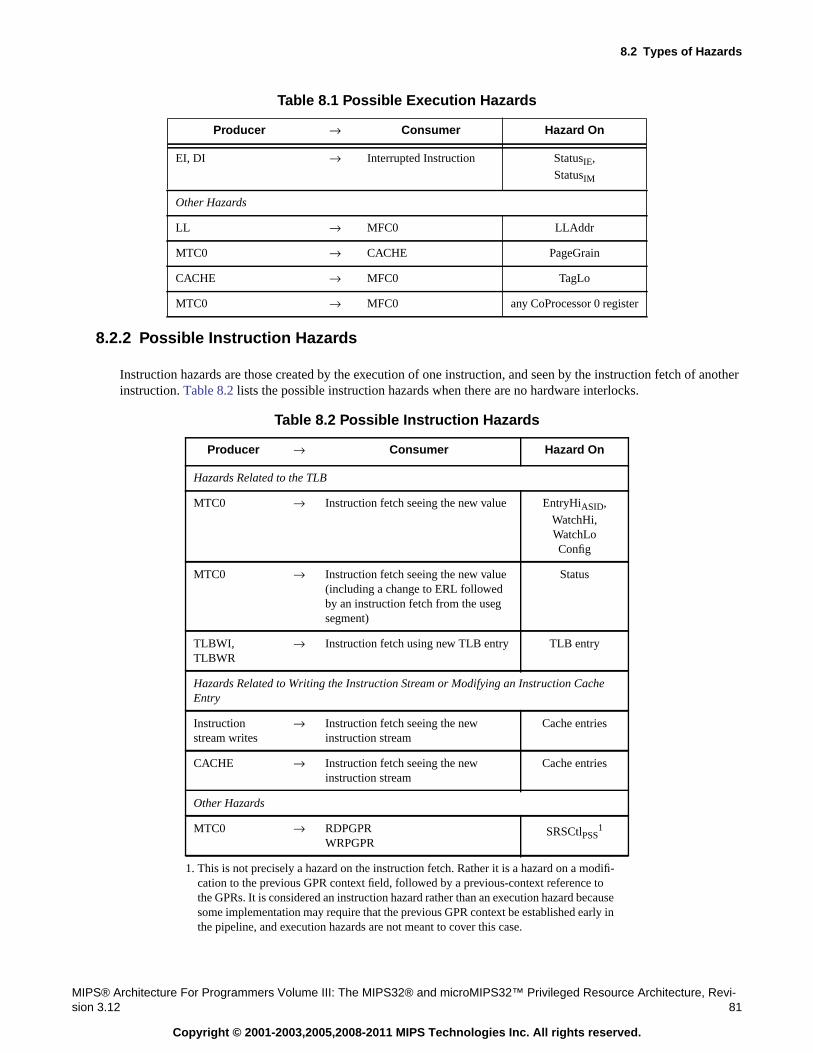
8.2 Types of Hazards
MIPS® Architecture For Programmers Volume III: The MIPS32® and microMIPS32™ Privileged Resource Architecture, Revi-sion 3.12 81
Copyright © 2001-2003,2005,2008-2011 MIPS Technologies Inc. All rights reserved.
8.2.2 Possible Instruction Hazards
Instruction hazards are those created by the execution of one instruction, and seen by the instruction fetch of anotherinstruction. Table 8.2 lists the possible instruction hazards when there are no hardware interlocks.
EI, DI → Interrupted Instruction StatusIE,
StatusIM
Other Hazards
LL → MFC0 LLAddr
MTC0 → CACHE PageGrain
CACHE → MFC0 TagLo
MTC0 → MFC0 any CoProcessor 0 register
Table 8.2 Possible Instruction Hazards
Producer → Consumer Hazard On
Hazards Related to the TLB
MTC0 → Instruction fetch seeing the new value EntryHiASID,
WatchHi,WatchLoConfig
MTC0 → Instruction fetch seeing the new value(including a change to ERL followedby an instruction fetch from the usegsegment)
Status
TLBWI,TLBWR
→ Instruction fetch using new TLB entry TLB entry
Hazards Related to Writing the Instruction Stream or Modifying an Instruction CacheEntry
Instructionstream writes
→ Instruction fetch seeing the newinstruction stream
Cache entries
CACHE → Instruction fetch seeing the newinstruction stream
Cache entries
Other Hazards
MTC0 → RDPGPRWRPGPR
SRSCtlPSS1
1. This is not precisely a hazard on the instruction fetch. Rather it is a hazard on a modifi-cation to the previous GPR context field, followed by a previous-context reference tothe GPRs. It is considered an instruction hazard rather than an execution hazard becausesome implementation may require that the previous GPR context be established early inthe pipeline, and execution hazards are not meant to cover this case.
Table 8.1 Possible Execution Hazards
Producer → Consumer Hazard On
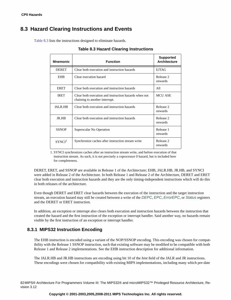
CP0 Hazards
82MIPS® Architecture For Programmers Volume III: The MIPS32® and microMIPS32™ Privileged Resource Architecture, Re-vision 3.12
Copyright © 2001-2003,2005,2008-2011 MIPS Technologies Inc. All rights reserved.
8.3 Hazard Clearing Instructions and Events
Table 8.3 lists the instructions designed to eliminate hazards.
DERET, ERET, and SSNOP are available in Release 1 of the Architecture; EHB, JALR.HB, JR.HB, and SYNCIwere added in Release 2 of the Architecture. In both Release 1 and Release 2 of the Architecture, DERET and ERETclear both execution and instruction hazards and they are the only timing-independent instructions which will do thisin both releases of the architecture.
Even though DERET and ERET clear hazards between the execution of the instruction and the target instructionstream, an execution hazard may still be created between a write of the DEPC, EPC, ErrorEPC, or Status registersand the DERET or ERET instruction.
In addition, an exception or interrupt also clears both execution and instruction hazards between the instruction thatcreated the hazard and the first instruction of the exception or interrupt handler. Said another way, no hazards remainvisible by the first instruction of an exception or interrupt handler.
8.3.1 MIPS32 Instruction Encoding
The EHB instruction is encoded using a variant of the NOP/SSNOP encoding. This encoding was chosen for compat-ibility with the Release 1 SSNOP instruction, such that existing software may be modified to be compatible with bothRelease 1 and Release 2 implementations. See the EHB instruction description for additional information.
The JALR.HB and JR.HB instructions are encoding using bit 10 of the hint field of the JALR and JR instructions.These encodings were chosen for compatibility with existing MIPS implementations, including many which pre-date
Table 8.3 Hazard Clearing Instructions
Mnemonic FunctionSupported
Architecture
DERET Clear both execution and instruction hazards EJTAG
EHB Clear execution hazard Release 2onwards
ERET Clear both execution and instruction hazards All
IRET Clear both execution and instruction hazards when notchaining to another interrupt.
MCU ASE
JALR.HB Clear both execution and instruction hazards Release 2onwards
JR.HB Clear both execution and instruction hazards Release 2onwards
SSNOP Superscalar No Operation Release 1onwards
SYNCI1
1. SYNCI synchronizes caches after an instruction stream write, and before execution of thatinstruction stream. As such, it is not precisely a coprocessor 0 hazard, but is included herefor completeness.
Synchronize caches after instruction stream write Release 2onwards
8.3 Hazard Clearing Instructions and Events
MIPS® Architecture For Programmers Volume III: The MIPS32® and microMIPS32™ Privileged Resource Architecture, Revi-sion 3.12 83
Copyright © 2001-2003,2005,2008-2011 MIPS Technologies Inc. All rights reserved.
the MIPS32 architecture. Because a pipeline flush clears hazards on most early implementations, the JALR.HB orJR.HB instructions can be included in existing software for backward and forward compatibility. See the JALR.HBand JR.HB instructions for additional information.
The SYNCI instruction is encoded using a new encoding of the REGIMM opcode. This encoding was chosenbecause it causes a Reserved Instruction exception on all Release 1 implementations. As such, kernel software run-ning on processors that don’t implement Release 2 can emulate the function using the CACHE instruction.
8.3.2 microMIPS32 Instruction Encoding
The EHB and SSNOP instructions are encoded using a variant of the NOP encoding. See the EHB and SSNOPinstruction description for additional information.

CP0 Hazards
84MIPS® Architecture For Programmers Volume III: The MIPS32® and microMIPS32™ Privileged Resource Architecture, Re-vision 3.12
Copyright © 2001-2003,2005,2008-2011 MIPS Technologies Inc. All rights reserved.
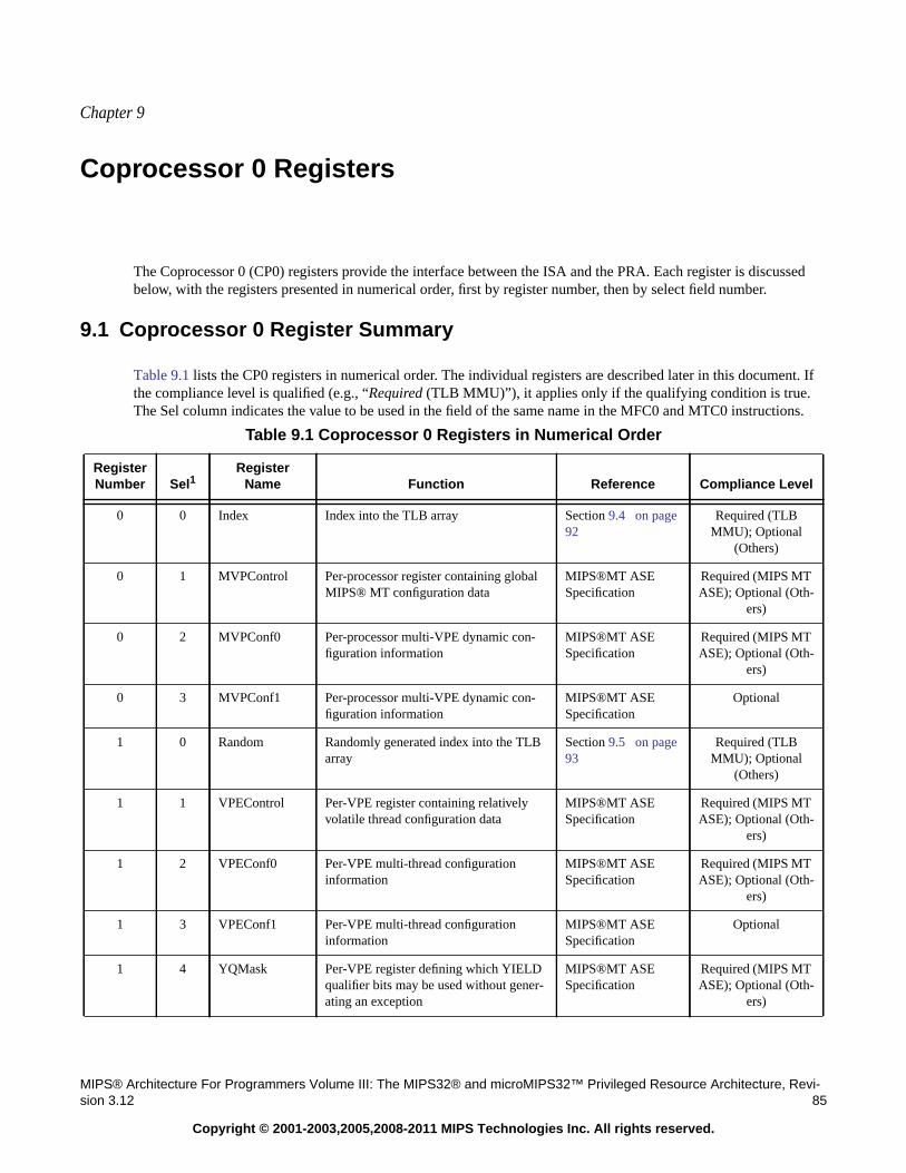
Chapter 9
MIPS® Architecture For Programmers Volume III: The MIPS32® and microMIPS32™ Privileged Resource Architecture, Revi-sion 3.12 85
Copyright © 2001-2003,2005,2008-2011 MIPS Technologies Inc. All rights reserved.
Coprocessor 0 Registers
The Coprocessor 0 (CP0) registers provide the interface between the ISA and the PRA. Each register is discussedbelow, with the registers presented in numerical order, first by register number, then by select field number.
9.1 Coprocessor 0 Register Summary
Table 9.1 lists the CP0 registers in numerical order. The individual registers are described later in this document. Ifthe compliance level is qualified (e.g., “Required (TLB MMU)”), it applies only if the qualifying condition is true.The Sel column indicates the value to be used in the field of the same name in the MFC0 and MTC0 instructions.
Table 9.1 Coprocessor 0 Registers in Numerical Order
RegisterNumber Sel1
RegisterName Function Reference Compliance Level
0 0 Index Index into the TLB array Section 9.4 on page92
Required (TLBMMU); Optional
(Others)
0 1 MVPControl Per-processor register containing globalMIPS® MT configuration data
MIPS®MT ASESpecification
Required (MIPS MTASE); Optional (Oth-
ers)
0 2 MVPConf0 Per-processor multi-VPE dynamic con-figuration information
MIPS®MT ASESpecification
Required (MIPS MTASE); Optional (Oth-
ers)
0 3 MVPConf1 Per-processor multi-VPE dynamic con-figuration information
MIPS®MT ASESpecification
Optional
1 0 Random Randomly generated index into the TLBarray
Section 9.5 on page93
Required (TLBMMU); Optional
(Others)
1 1 VPEControl Per-VPE register containing relativelyvolatile thread configuration data
MIPS®MT ASESpecification
Required (MIPS MTASE); Optional (Oth-
ers)
1 2 VPEConf0 Per-VPE multi-thread configurationinformation
MIPS®MT ASESpecification
Required (MIPS MTASE); Optional (Oth-
ers)
1 3 VPEConf1 Per-VPE multi-thread configurationinformation
MIPS®MT ASESpecification
Optional
1 4 YQMask Per-VPE register defining which YIELDqualifier bits may be used without gener-ating an exception
MIPS®MT ASESpecification
Required (MIPS MTASE); Optional (Oth-
ers)
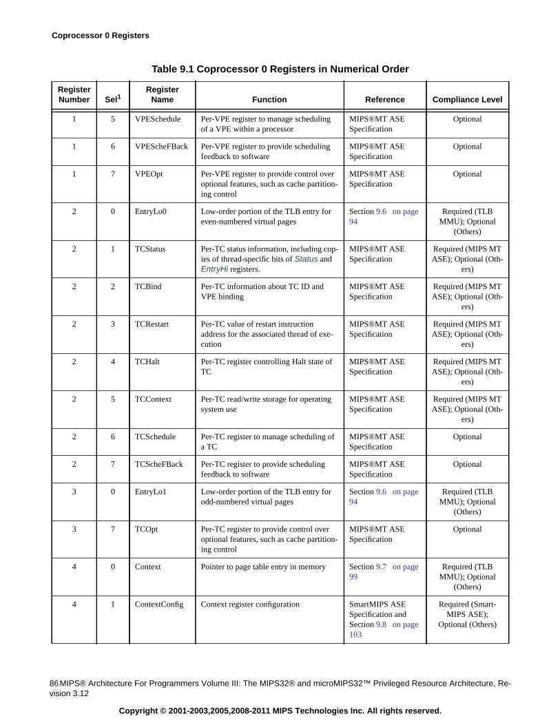
Coprocessor 0 Registers
86MIPS® Architecture For Programmers Volume III: The MIPS32® and microMIPS32™ Privileged Resource Architecture, Re-vision 3.12
Copyright © 2001-2003,2005,2008-2011 MIPS Technologies Inc. All rights reserved.
1 5 VPESchedule Per-VPE register to manage schedulingof a VPE within a processor
MIPS®MT ASESpecification
Optional
1 6 VPEScheFBack Per-VPE register to provide schedulingfeedback to software
MIPS®MT ASESpecification
Optional
1 7 VPEOpt Per-VPE register to provide control overoptional features, such as cache partition-ing control
MIPS®MT ASESpecification
Optional
2 0 EntryLo0 Low-order portion of the TLB entry foreven-numbered virtual pages
Section 9.6 on page94
Required (TLBMMU); Optional
(Others)
2 1 TCStatus Per-TC status information, including cop-ies of thread-specific bits of Status andEntryHi registers.
MIPS®MT ASESpecification
Required (MIPS MTASE); Optional (Oth-
ers)
2 2 TCBind Per-TC information about TC ID andVPE binding
MIPS®MT ASESpecification
Required (MIPS MTASE); Optional (Oth-
ers)
2 3 TCRestart Per-TC value of restart instructionaddress for the associated thread of exe-cution
MIPS®MT ASESpecification
Required (MIPS MTASE); Optional (Oth-
ers)
2 4 TCHalt Per-TC register controlling Halt state ofTC
MIPS®MT ASESpecification
Required (MIPS MTASE); Optional (Oth-
ers)
2 5 TCContext Per-TC read/write storage for operatingsystem use
MIPS®MT ASESpecification
Required (MIPS MTASE); Optional (Oth-
ers)
2 6 TCSchedule Per-TC register to manage scheduling ofa TC
MIPS®MT ASESpecification
Optional
2 7 TCScheFBack Per-TC register to provide schedulingfeedback to software
MIPS®MT ASESpecification
Optional
3 0 EntryLo1 Low-order portion of the TLB entry forodd-numbered virtual pages
Section 9.6 on page94
Required (TLBMMU); Optional
(Others)
3 7 TCOpt Per-TC register to provide control overoptional features, such as cache partition-ing control
MIPS®MT ASESpecification
Optional
4 0 Context Pointer to page table entry in memory Section 9.7 on page99
Required (TLBMMU); Optional
(Others)
4 1 ContextConfig Context register configuration SmartMIPS ASESpecification andSection 9.8 on page103
Required (Smart-MIPS ASE);
Optional (Others)
Table 9.1 Coprocessor 0 Registers in Numerical Order
RegisterNumber Sel1
RegisterName Function Reference Compliance Level
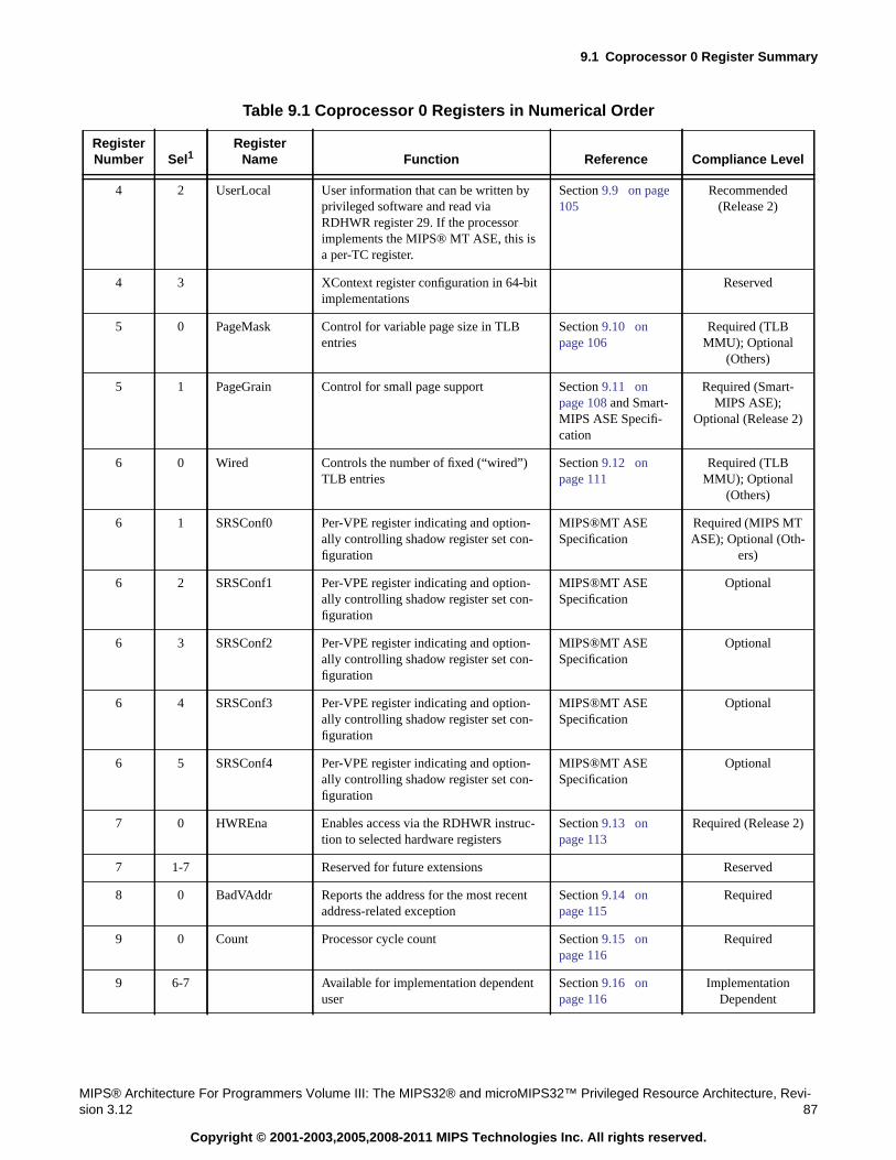
9.1 Coprocessor 0 Register Summary
MIPS® Architecture For Programmers Volume III: The MIPS32® and microMIPS32™ Privileged Resource Architecture, Revi-sion 3.12 87
Copyright © 2001-2003,2005,2008-2011 MIPS Technologies Inc. All rights reserved.
4 2 UserLocal User information that can be written byprivileged software and read viaRDHWR register 29. If the processorimplements the MIPS® MT ASE, this isa per-TC register.
Section 9.9 on page105
Recommended(Release 2)
4 3 XContext register configuration in 64-bitimplementations
Reserved
5 0 PageMask Control for variable page size in TLBentries
Section 9.10 onpage 106
Required (TLBMMU); Optional
(Others)
5 1 PageGrain Control for small page support Section 9.11 onpage 108 and Smart-MIPS ASE Specifi-cation
Required (Smart-MIPS ASE);
Optional (Release 2)
6 0 Wired Controls the number of fixed (“wired”)TLB entries
Section 9.12 onpage 111
Required (TLBMMU); Optional
(Others)
6 1 SRSConf0 Per-VPE register indicating and option-ally controlling shadow register set con-figuration
MIPS®MT ASESpecification
Required (MIPS MTASE); Optional (Oth-
ers)
6 2 SRSConf1 Per-VPE register indicating and option-ally controlling shadow register set con-figuration
MIPS®MT ASESpecification
Optional
6 3 SRSConf2 Per-VPE register indicating and option-ally controlling shadow register set con-figuration
MIPS®MT ASESpecification
Optional
6 4 SRSConf3 Per-VPE register indicating and option-ally controlling shadow register set con-figuration
MIPS®MT ASESpecification
Optional
6 5 SRSConf4 Per-VPE register indicating and option-ally controlling shadow register set con-figuration
MIPS®MT ASESpecification
Optional
7 0 HWREna Enables access via the RDHWR instruc-tion to selected hardware registers
Section 9.13 onpage 113
Required (Release 2)
7 1-7 Reserved for future extensions Reserved
8 0 BadVAddr Reports the address for the most recentaddress-related exception
Section 9.14 onpage 115
Required
9 0 Count Processor cycle count Section 9.15 onpage 116
Required
9 6-7 Available for implementation dependentuser
Section 9.16 onpage 116
ImplementationDependent
Table 9.1 Coprocessor 0 Registers in Numerical Order
RegisterNumber Sel1
RegisterName Function Reference Compliance Level
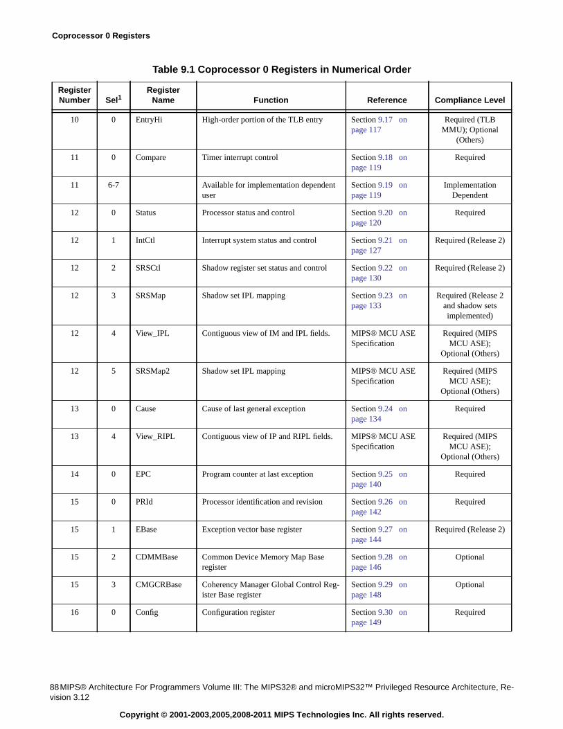
Coprocessor 0 Registers
88MIPS® Architecture For Programmers Volume III: The MIPS32® and microMIPS32™ Privileged Resource Architecture, Re-vision 3.12
Copyright © 2001-2003,2005,2008-2011 MIPS Technologies Inc. All rights reserved.
10 0 EntryHi High-order portion of the TLB entry Section 9.17 onpage 117
Required (TLBMMU); Optional
(Others)
11 0 Compare Timer interrupt control Section 9.18 onpage 119
Required
11 6-7 Available for implementation dependentuser
Section 9.19 onpage 119
ImplementationDependent
12 0 Status Processor status and control Section 9.20 onpage 120
Required
12 1 IntCtl Interrupt system status and control Section 9.21 onpage 127
Required (Release 2)
12 2 SRSCtl Shadow register set status and control Section 9.22 onpage 130
Required (Release 2)
12 3 SRSMap Shadow set IPL mapping Section 9.23 onpage 133
Required (Release 2and shadow setsimplemented)
12 4 View_IPL Contiguous view of IM and IPL fields. MIPS® MCU ASESpecification
Required (MIPSMCU ASE);
Optional (Others)
12 5 SRSMap2 Shadow set IPL mapping MIPS® MCU ASESpecification
Required (MIPSMCU ASE);
Optional (Others)
13 0 Cause Cause of last general exception Section 9.24 onpage 134
Required
13 4 View_RIPL Contiguous view of IP and RIPL fields. MIPS® MCU ASESpecification
Required (MIPSMCU ASE);
Optional (Others)
14 0 EPC Program counter at last exception Section 9.25 onpage 140
Required
15 0 PRId Processor identification and revision Section 9.26 onpage 142
Required
15 1 EBase Exception vector base register Section 9.27 onpage 144
Required (Release 2)
15 2 CDMMBase Common Device Memory Map Baseregister
Section 9.28 onpage 146
Optional
15 3 CMGCRBase Coherency Manager Global Control Reg-ister Base register
Section 9.29 onpage 148
Optional
16 0 Config Configuration register Section 9.30 onpage 149
Required
Table 9.1 Coprocessor 0 Registers in Numerical Order
RegisterNumber Sel1
RegisterName Function Reference Compliance Level
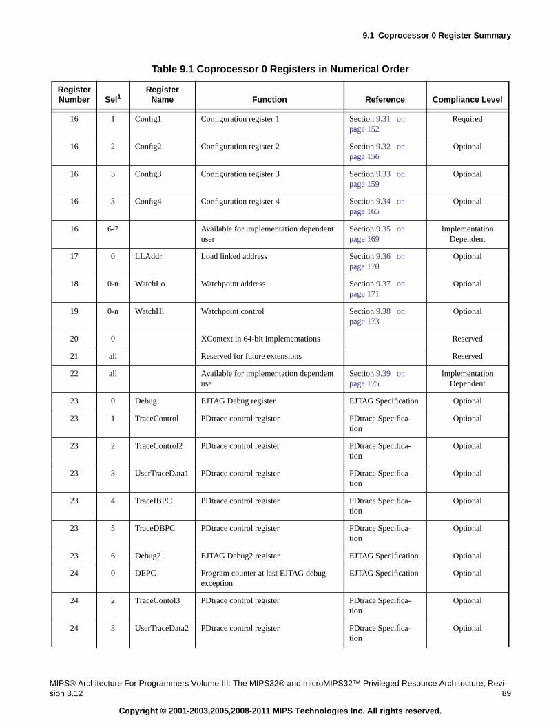
9.1 Coprocessor 0 Register Summary
MIPS® Architecture For Programmers Volume III: The MIPS32® and microMIPS32™ Privileged Resource Architecture, Revi-sion 3.12 89
Copyright © 2001-2003,2005,2008-2011 MIPS Technologies Inc. All rights reserved.
16 1 Config1 Configuration register 1 Section 9.31 onpage 152
Required
16 2 Config2 Configuration register 2 Section 9.32 onpage 156
Optional
16 3 Config3 Configuration register 3 Section 9.33 onpage 159
Optional
16 3 Config4 Configuration register 4 Section 9.34 onpage 165
Optional
16 6-7 Available for implementation dependentuser
Section 9.35 onpage 169
ImplementationDependent
17 0 LLAddr Load linked address Section 9.36 onpage 170
Optional
18 0-n WatchLo Watchpoint address Section 9.37 onpage 171
Optional
19 0-n WatchHi Watchpoint control Section 9.38 onpage 173
Optional
20 0 XContext in 64-bit implementations Reserved
21 all Reserved for future extensions Reserved
22 all Available for implementation dependentuse
Section 9.39 onpage 175
ImplementationDependent
23 0 Debug EJTAG Debug register EJTAG Specification Optional
23 1 TraceControl PDtrace control register PDtrace Specifica-tion
Optional
23 2 TraceControl2 PDtrace control register PDtrace Specifica-tion
Optional
23 3 UserTraceData1 PDtrace control register PDtrace Specifica-tion
Optional
23 4 TraceIBPC PDtrace control register PDtrace Specifica-tion
Optional
23 5 TraceDBPC PDtrace control register PDtrace Specifica-tion
Optional
23 6 Debug2 EJTAG Debug2 register EJTAG Specification Optional
24 0 DEPC Program counter at last EJTAG debugexception
EJTAG Specification Optional
24 2 TraceContol3 PDtrace control register PDtrace Specifica-tion
Optional
24 3 UserTraceData2 PDtrace control register PDtrace Specifica-tion
Optional
Table 9.1 Coprocessor 0 Registers in Numerical Order
RegisterNumber Sel1
RegisterName Function Reference Compliance Level
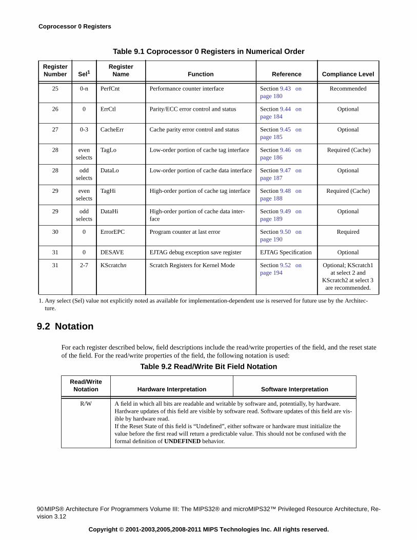
Coprocessor 0 Registers
90MIPS® Architecture For Programmers Volume III: The MIPS32® and microMIPS32™ Privileged Resource Architecture, Re-vision 3.12
Copyright © 2001-2003,2005,2008-2011 MIPS Technologies Inc. All rights reserved.
9.2 Notation
For each register described below, field descriptions include the read/write properties of the field, and the reset stateof the field. For the read/write properties of the field, the following notation is used:
25 0-n PerfCnt Performance counter interface Section 9.43 onpage 180
Recommended
26 0 ErrCtl Parity/ECC error control and status Section 9.44 onpage 184
Optional
27 0-3 CacheErr Cache parity error control and status Section 9.45 onpage 185
Optional
28 evenselects
TagLo Low-order portion of cache tag interface Section 9.46 onpage 186
Required (Cache)
28 oddselects
DataLo Low-order portion of cache data interface Section 9.47 onpage 187
Optional
29 evenselects
TagHi High-order portion of cache tag interface Section 9.48 onpage 188
Required (Cache)
29 oddselects
DataHi High-order portion of cache data inter-face
Section 9.49 onpage 189
Optional
30 0 ErrorEPC Program counter at last error Section 9.50 onpage 190
Required
31 0 DESAVE EJTAG debug exception save register EJTAG Specification Optional
31 2-7 KScratchn Scratch Registers for Kernel Mode Section 9.52 onpage 194
Optional; KScratch1at select 2 and
KScratch2 at select 3are recommended.
1. Any select (Sel) value not explicitly noted as available for implementation-dependent use is reserved for future use by the Architec-ture.
Table 9.2 Read/Write Bit Field Notation
Read/WriteNotation Hardware Interpretation Software Interpretation
R/W A field in which all bits are readable and writable by software and, potentially, by hardware.Hardware updates of this field are visible by software read. Software updates of this field are vis-ible by hardware read.If the Reset State of this field is “Undefined”, either software or hardware must initialize thevalue before the first read will return a predictable value. This should not be confused with theformal definition of UNDEFINED behavior.
Table 9.1 Coprocessor 0 Registers in Numerical Order
RegisterNumber Sel1
RegisterName Function Reference Compliance Level
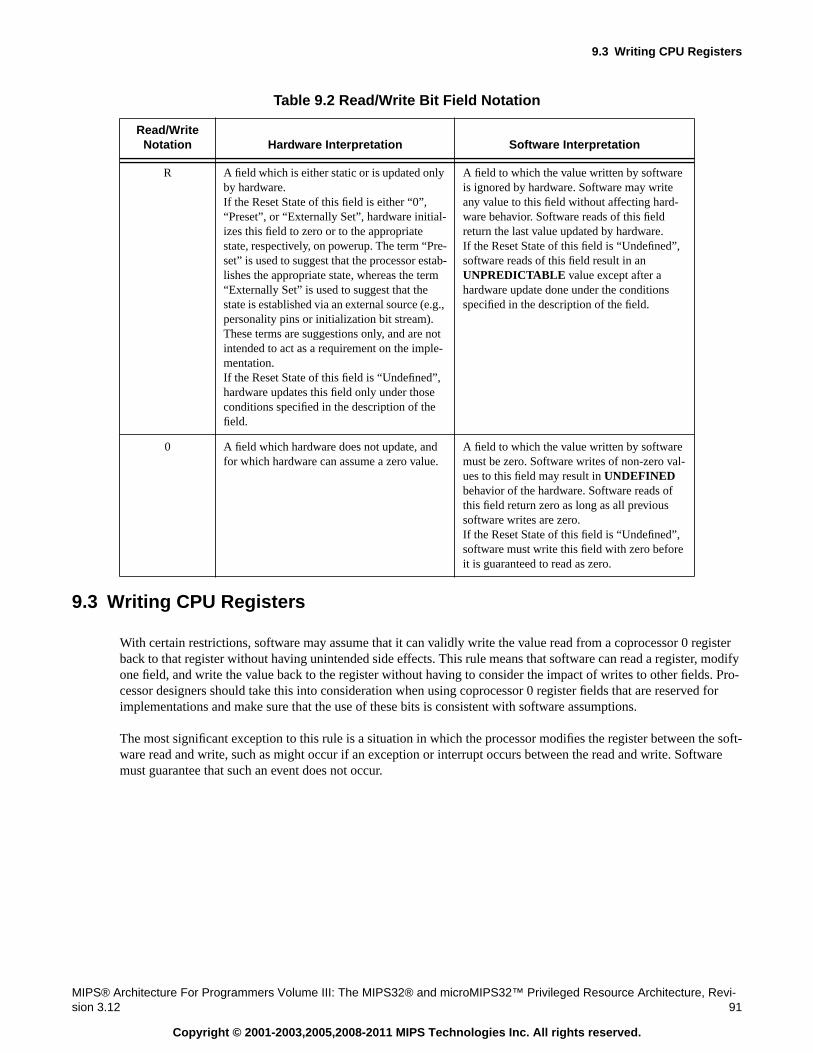
9.3 Writing CPU Registers
MIPS® Architecture For Programmers Volume III: The MIPS32® and microMIPS32™ Privileged Resource Architecture, Revi-sion 3.12 91
Copyright © 2001-2003,2005,2008-2011 MIPS Technologies Inc. All rights reserved.
9.3 Writing CPU Registers
With certain restrictions, software may assume that it can validly write the value read from a coprocessor 0 registerback to that register without having unintended side effects. This rule means that software can read a register, modifyone field, and write the value back to the register without having to consider the impact of writes to other fields. Pro-cessor designers should take this into consideration when using coprocessor 0 register fields that are reserved forimplementations and make sure that the use of these bits is consistent with software assumptions.
The most significant exception to this rule is a situation in which the processor modifies the register between the soft-ware read and write, such as might occur if an exception or interrupt occurs between the read and write. Softwaremust guarantee that such an event does not occur.
R A field which is either static or is updated onlyby hardware.If the Reset State of this field is either “0”,“Preset”, or “Externally Set”, hardware initial-izes this field to zero or to the appropriatestate, respectively, on powerup. The term “Pre-set” is used to suggest that the processor estab-lishes the appropriate state, whereas the term“Externally Set” is used to suggest that thestate is established via an external source (e.g.,personality pins or initialization bit stream).These terms are suggestions only, and are notintended to act as a requirement on the imple-mentation.If the Reset State of this field is “Undefined”,hardware updates this field only under thoseconditions specified in the description of thefield.
A field to which the value written by softwareis ignored by hardware. Software may writeany value to this field without affecting hard-ware behavior. Software reads of this fieldreturn the last value updated by hardware.If the Reset State of this field is “Undefined”,software reads of this field result in anUNPREDICTABLE value except after ahardware update done under the conditionsspecified in the description of the field.
0 A field which hardware does not update, andfor which hardware can assume a zero value.
A field to which the value written by softwaremust be zero. Software writes of non-zero val-ues to this field may result in UNDEFINEDbehavior of the hardware. Software reads ofthis field return zero as long as all previoussoftware writes are zero.If the Reset State of this field is “Undefined”,software must write this field with zero beforeit is guaranteed to read as zero.
Table 9.2 Read/Write Bit Field Notation
Read/WriteNotation Hardware Interpretation Software Interpretation
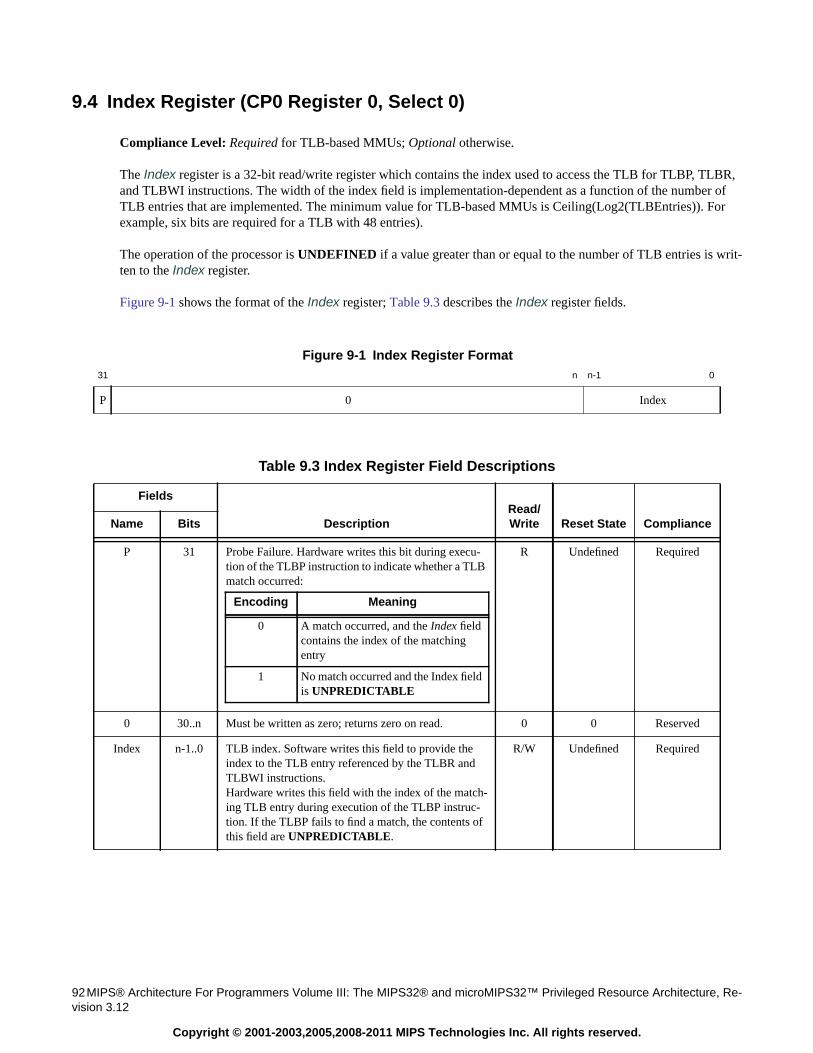
92MIPS® Architecture For Programmers Volume III: The MIPS32® and microMIPS32™ Privileged Resource Architecture, Re-vision 3.12
Copyright © 2001-2003,2005,2008-2011 MIPS Technologies Inc. All rights reserved.
9.4 Index Register (CP0 Register 0, Select 0)
Compliance Level: Required for TLB-based MMUs; Optional otherwise.
The Index register is a 32-bit read/write register which contains the index used to access the TLB for TLBP, TLBR,and TLBWI instructions. The width of the index field is implementation-dependent as a function of the number ofTLB entries that are implemented. The minimum value for TLB-based MMUs is Ceiling(Log2(TLBEntries)). Forexample, six bits are required for a TLB with 48 entries).
The operation of the processor is UNDEFINED if a value greater than or equal to the number of TLB entries is writ-ten to the Index register.
Figure 9-1 shows the format of the Index register; Table 9.3 describes the Index register fields.
Figure 9-1 Index Register Format31 n n-1 0
P 0 Index
Table 9.3 Index Register Field Descriptions
Fields
DescriptionRead/Write Reset State ComplianceName Bits
P 31 Probe Failure. Hardware writes this bit during execu-tion of the TLBP instruction to indicate whether a TLBmatch occurred:
R Undefined Required
0 30..n Must be written as zero; returns zero on read. 0 0 Reserved
Index n-1..0 TLB index. Software writes this field to provide theindex to the TLB entry referenced by the TLBR andTLBWI instructions.Hardware writes this field with the index of the match-ing TLB entry during execution of the TLBP instruc-tion. If the TLBP fails to find a match, the contents ofthis field are UNPREDICTABLE.
R/W Undefined Required
Encoding Meaning
0 A match occurred, and the Index fieldcontains the index of the matchingentry
1 No match occurred and the Index fieldis UNPREDICTABLE
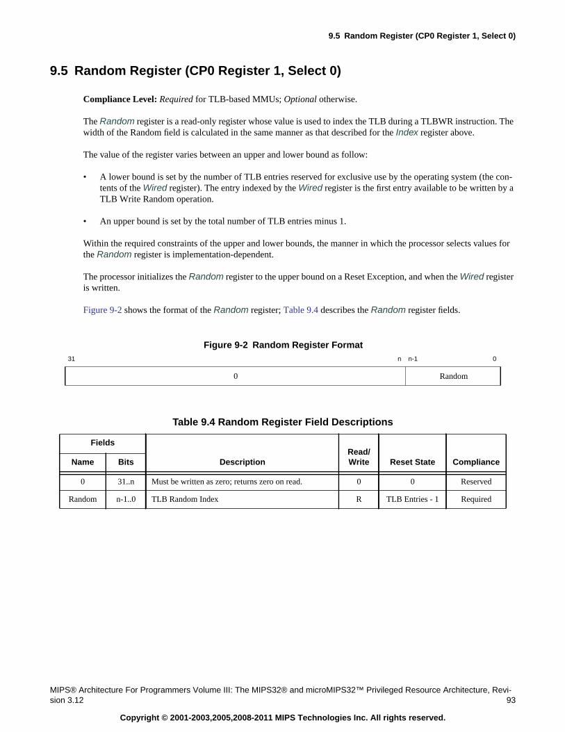
9.5 Random Register (CP0 Register 1, Select 0)
MIPS® Architecture For Programmers Volume III: The MIPS32® and microMIPS32™ Privileged Resource Architecture, Revi-sion 3.12 93
Copyright © 2001-2003,2005,2008-2011 MIPS Technologies Inc. All rights reserved.
9.5 Random Register (CP0 Register 1, Select 0)
Compliance Level: Required for TLB-based MMUs; Optional otherwise.
The Random register is a read-only register whose value is used to index the TLB during a TLBWR instruction. Thewidth of the Random field is calculated in the same manner as that described for the Index register above.
The value of the register varies between an upper and lower bound as follow:
• A lower bound is set by the number of TLB entries reserved for exclusive use by the operating system (the con-tents of the Wired register). The entry indexed by the Wired register is the first entry available to be written by aTLB Write Random operation.
• An upper bound is set by the total number of TLB entries minus 1.
Within the required constraints of the upper and lower bounds, the manner in which the processor selects values forthe Random register is implementation-dependent.
The processor initializes the Random register to the upper bound on a Reset Exception, and when the Wired registeris written.
Figure 9-2 shows the format of the Random register; Table 9.4 describes the Random register fields.
Figure 9-2 Random Register Format31 n n-1 0
0 Random
Table 9.4 Random Register Field Descriptions
Fields
DescriptionRead/Write Reset State ComplianceName Bits
0 31..n Must be written as zero; returns zero on read. 0 0 Reserved
Random n-1..0 TLB Random Index R TLB Entries - 1 Required
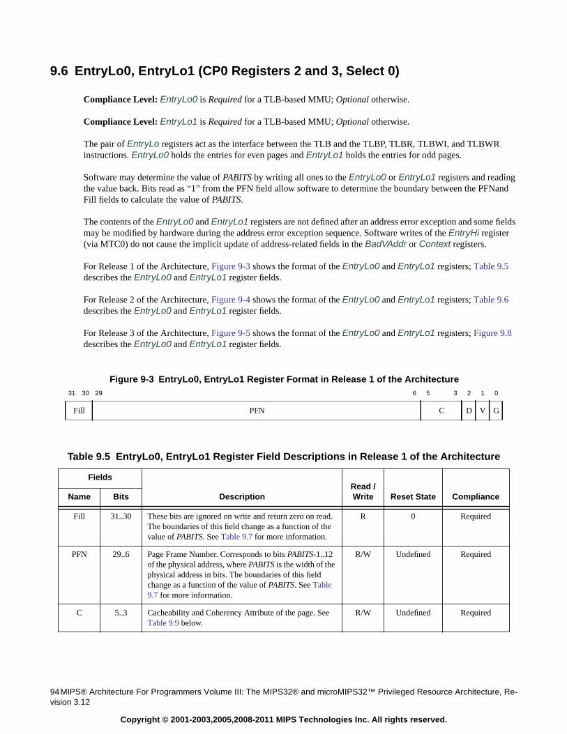
94MIPS® Architecture For Programmers Volume III: The MIPS32® and microMIPS32™ Privileged Resource Architecture, Re-vision 3.12
Copyright © 2001-2003,2005,2008-2011 MIPS Technologies Inc. All rights reserved.
9.6 EntryLo0, EntryLo1 (CP0 Registers 2 and 3, Select 0)
Compliance Level: EntryLo0 is Required for a TLB-based MMU; Optional otherwise.
Compliance Level: EntryLo1 is Required for a TLB-based MMU; Optional otherwise.
The pair of EntryLo registers act as the interface between the TLB and the TLBP, TLBR, TLBWI, and TLBWRinstructions. EntryLo0 holds the entries for even pages and EntryLo1 holds the entries for odd pages.
Software may determine the value of PABITS by writing all ones to the EntryLo0 or EntryLo1 registers and readingthe value back. Bits read as “1” from the PFN field allow software to determine the boundary between the PFNandFill fields to calculate the value of PABITS.
The contents of the EntryLo0 and EntryLo1 registers are not defined after an address error exception and some fieldsmay be modified by hardware during the address error exception sequence. Software writes of the EntryHi register(via MTC0) do not cause the implicit update of address-related fields in the BadVAddr or Context registers.
For Release 1 of the Architecture, Figure 9-3 shows the format of the EntryLo0 and EntryLo1 registers; Table 9.5describes the EntryLo0 and EntryLo1 register fields.
For Release 2 of the Architecture, Figure 9-4 shows the format of the EntryLo0 and EntryLo1 registers; Table 9.6describes the EntryLo0 and EntryLo1 register fields.
For Release 3 of the Architecture, Figure 9-5 shows the format of the EntryLo0 and EntryLo1 registers; Figure 9.8describes the EntryLo0 and EntryLo1 register fields.
Figure 9-3 EntryLo0, EntryLo1 Register Format in Release 1 of the Architecture31 30 29 6 5 3 2 1 0
Fill PFN C D V G
Table 9.5 EntryLo0, EntryLo1 Register Field Descriptions in Release 1 of the Architecture
Fields
DescriptionRead /Write Reset State ComplianceName Bits
Fill 31..30 These bits are ignored on write and return zero on read.The boundaries of this field change as a function of thevalue of PABITS. See Table 9.7 for more information.
R 0 Required
PFN 29..6 Page Frame Number. Corresponds to bits PABITS-1..12of the physical address, where PABITS is the width of thephysical address in bits. The boundaries of this fieldchange as a function of the value of PABITS. See Table9.7 for more information.
R/W Undefined Required
C 5..3 Cacheability and Coherency Attribute of the page. SeeTable 9.9 below.
R/W Undefined Required
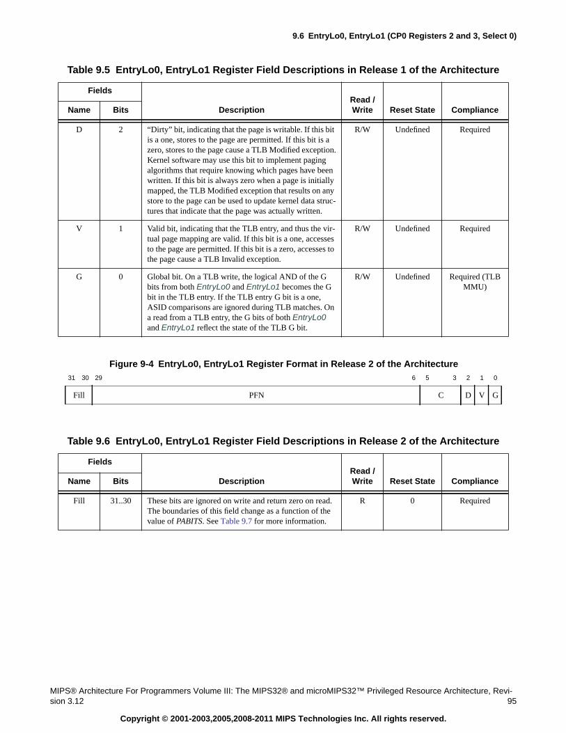
9.6 EntryLo0, EntryLo1 (CP0 Registers 2 and 3, Select 0)
MIPS® Architecture For Programmers Volume III: The MIPS32® and microMIPS32™ Privileged Resource Architecture, Revi-sion 3.12 95
Copyright © 2001-2003,2005,2008-2011 MIPS Technologies Inc. All rights reserved.
D 2 “Dirty” bit, indicating that the page is writable. If this bitis a one, stores to the page are permitted. If this bit is azero, stores to the page cause a TLB Modified exception.Kernel software may use this bit to implement pagingalgorithms that require knowing which pages have beenwritten. If this bit is always zero when a page is initiallymapped, the TLB Modified exception that results on anystore to the page can be used to update kernel data struc-tures that indicate that the page was actually written.
R/W Undefined Required
V 1 Valid bit, indicating that the TLB entry, and thus the vir-tual page mapping are valid. If this bit is a one, accessesto the page are permitted. If this bit is a zero, accesses tothe page cause a TLB Invalid exception.
R/W Undefined Required
G 0 Global bit. On a TLB write, the logical AND of the Gbits from both EntryLo0 and EntryLo1 becomes the Gbit in the TLB entry. If the TLB entry G bit is a one,ASID comparisons are ignored during TLB matches. Ona read from a TLB entry, the G bits of both EntryLo0and EntryLo1 reflect the state of the TLB G bit.
R/W Undefined Required (TLBMMU)
Figure 9-4 EntryLo0, EntryLo1 Register Format in Release 2 of the Architecture31 30 29 6 5 3 2 1 0
Fill PFN C D V G
Table 9.6 EntryLo0, EntryLo1 Register Field Descriptions in Release 2 of the Architecture
Fields
DescriptionRead /Write Reset State ComplianceName Bits
Fill 31..30 These bits are ignored on write and return zero on read.The boundaries of this field change as a function of thevalue of PABITS. See Table 9.7 for more information.
R 0 Required
Table 9.5 EntryLo0, EntryLo1 Register Field Descriptions in Release 1 of the Architecture
Fields
DescriptionRead /Write Reset State ComplianceName Bits
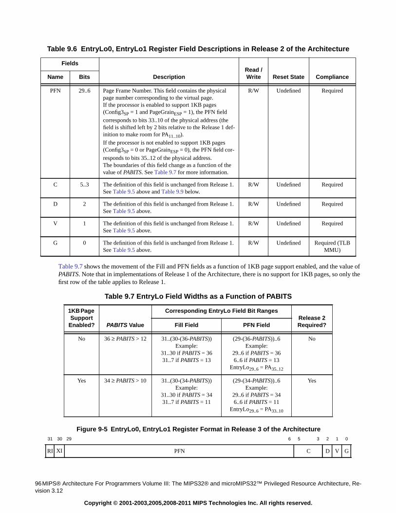
96MIPS® Architecture For Programmers Volume III: The MIPS32® and microMIPS32™ Privileged Resource Architecture, Re-vision 3.12
Copyright © 2001-2003,2005,2008-2011 MIPS Technologies Inc. All rights reserved.
Table 9.7 shows the movement of the Fill and PFN fields as a function of 1KB page support enabled, and the value ofPABITS. Note that in implementations of Release 1 of the Architecture, there is no support for 1KB pages, so only thefirst row of the table applies to Release 1.
PFN 29..6 Page Frame Number. This field contains the physicalpage number corresponding to the virtual page.If the processor is enabled to support 1KB pages(Config3SP = 1 and PageGrainESP = 1), the PFN field
corresponds to bits 33..10 of the physical address (thefield is shifted left by 2 bits relative to the Release 1 def-inition to make room for PA11..10).
If the processor is not enabled to support 1KB pages(Config3SP = 0 or PageGrainESP = 0), the PFN field cor-
responds to bits 35..12 of the physical address.The boundaries of this field change as a function of thevalue of PABITS. See Table 9.7 for more information.
R/W Undefined Required
C 5..3 The definition of this field is unchanged from Release 1.See Table 9.5 above and Table 9.9 below.
R/W Undefined Required
D 2 The definition of this field is unchanged from Release 1.See Table 9.5 above.
R/W Undefined Required
V 1 The definition of this field is unchanged from Release 1.See Table 9.5 above.
R/W Undefined Required
G 0 The definition of this field is unchanged from Release 1.See Table 9.5 above.
R/W Undefined Required (TLBMMU)
Table 9.7 EntryLo Field Widths as a Function of PABITS
1KB PageSupport
Enabled? PABITS Value
Corresponding EntryLo Field Bit RangesRelease 2Required?Fill Field PFN Field
No 36 ≥ PABITS > 12 31..(30-(36-PABITS))Example:
31..30 if PABITS = 3631..7 if PABITS = 13
(29-(36-PABITS))..6Example:
29..6 if PABITS = 366..6 if PABITS = 13
EntryLo29..6 = PA35..12
No
Yes 34 ≥ PABITS > 10 31..(30-(34-PABITS))Example:
31..30 if PABITS = 3431..7 if PABITS = 11
(29-(34-PABITS))..6Example:
29..6 if PABITS = 346..6 if PABITS = 11
EntryLo29..6 = PA33..10
Yes
Figure 9-5 EntryLo0, EntryLo1 Register Format in Release 3 of the Architecture31 30 29 6 5 3 2 1 0
RI XI PFN C D V G
Table 9.6 EntryLo0, EntryLo1 Register Field Descriptions in Release 2 of the Architecture
Fields
DescriptionRead /Write Reset State ComplianceName Bits
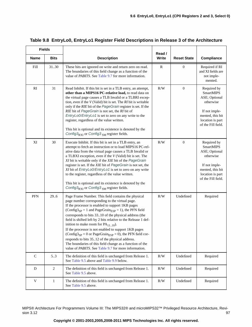
9.6 EntryLo0, EntryLo1 (CP0 Registers 2 and 3, Select 0)
MIPS® Architecture For Programmers Volume III: The MIPS32® and microMIPS32™ Privileged Resource Architecture, Revi-sion 3.12 97
Copyright © 2001-2003,2005,2008-2011 MIPS Technologies Inc. All rights reserved.
Table 9.8 EntryLo0, EntryLo1 Register Field Descriptions in Release 3 of the Architecture
Fields
DescriptionRead /Write Reset State ComplianceName Bits
Fill 31..30 These bits are ignored on write and return zero on read.The boundaries of this field change as a function of thevalue of PABITS. See Table 9.7 for more information.
R 0 Required if RIand XI fields are
not imple-mented.
RI 31 Read Inhibit. If this bit is set in a TLB entry, an attempt,other than a MIPS16 PC-relative load, to read data onthe virtual page causes a TLB Invalid or a TLBRI excep-tion, even if the V (Valid) bit is set. The RI bit is writableonly if the RIE bit of the PageGrain register is set. If theRIE bit of PageGrain is not set, the RI bit ofEntryLo0/EntryLo1 is set to zero on any write to theregister, regardless of the value written.
This bit is optional and its existence is denoted by theConfig3RXI or Config3 SM register fields.
R/W 0 Required bySmartMIPS
ASE; Optionalotherwise
If not imple-mented, this bitlocation is partof the Fill field.
XI 30 Execute Inhibit. If this bit is set in a TLB entry, anattempt to fetch an instruction or to load MIPS16 PC-rel-ative data from the virtual page causes a TLB Invalid ora TLBXI exception, even if the V (Valid) bit is set. TheXI bit is writable only if the XIE bit of the PageGrainregister is set. If the XIE bit of PageGrain is not set, theXI bit of EntryLo0/EntryLo1 is set to zero on any writeto the register, regardless of the value written.
This bit is optional and its existence is denoted by theConfig3RXI or Config3 SM register fields.
R/W 0 Required bySmartMIPS
ASE; Optionalotherwise
If not imple-mented, this bitlocation is partof the Fill field.
PFN 29..6 Page Frame Number. This field contains the physicalpage number corresponding to the virtual page.If the processor is enabled to support 1KB pages(Config3SP = 1 and PageGrainESP = 1), the PFN field
corresponds to bits 33..10 of the physical address (thefield is shifted left by 2 bits relative to the Release 1 def-inition to make room for PA11..10).
If the processor is not enabled to support 1KB pages(Config3SP = 0 or PageGrainESP = 0), the PFN field cor-
responds to bits 35..12 of the physical address.The boundaries of this field change as a function of thevalue of PABITS. See Table 9.7 for more information.
R/W Undefined Required
C 5..3 The definition of this field is unchanged from Release 1.See Table 9.5 above and Table 9.9 below.
R/W Undefined Required
D 2 The definition of this field is unchanged from Release 1.See Table 9.5 above.
R/W Undefined Required
V 1 The definition of this field is unchanged from Release 1.See Table 9.5 above.
R/W Undefined Required
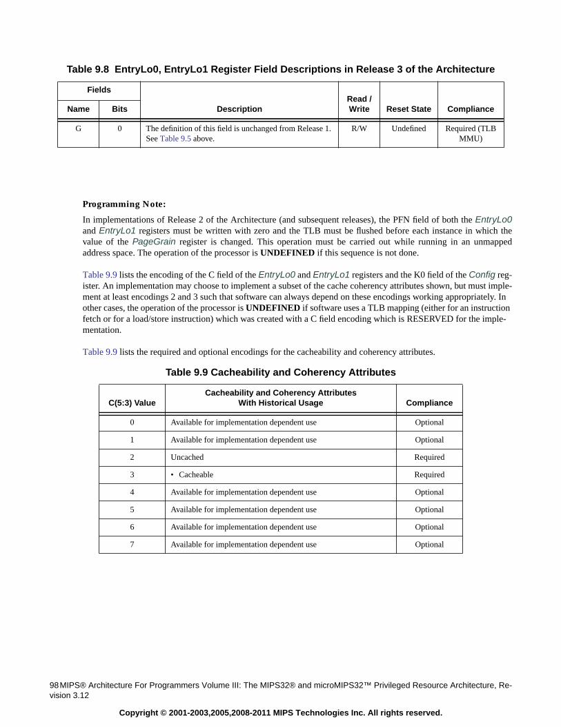
98MIPS® Architecture For Programmers Volume III: The MIPS32® and microMIPS32™ Privileged Resource Architecture, Re-vision 3.12
Copyright © 2001-2003,2005,2008-2011 MIPS Technologies Inc. All rights reserved.
Programming Note:
In implementations of Release 2 of the Architecture (and subsequent releases), the PFN field of both the EntryLo0and EntryLo1 registers must be written with zero and the TLB must be flushed before each instance in which thevalue of the PageGrain register is changed. This operation must be carried out while running in an unmappedaddress space. The operation of the processor is UNDEFINED if this sequence is not done.
Table 9.9 lists the encoding of the C field of the EntryLo0 and EntryLo1 registers and the K0 field of the Config reg-ister. An implementation may choose to implement a subset of the cache coherency attributes shown, but must imple-ment at least encodings 2 and 3 such that software can always depend on these encodings working appropriately. Inother cases, the operation of the processor is UNDEFINED if software uses a TLB mapping (either for an instructionfetch or for a load/store instruction) which was created with a C field encoding which is RESERVED for the imple-mentation.
Table 9.9 lists the required and optional encodings for the cacheability and coherency attributes.
G 0 The definition of this field is unchanged from Release 1.See Table 9.5 above.
R/W Undefined Required (TLBMMU)
Table 9.9 Cacheability and Coherency Attributes
C(5:3) ValueCacheability and Coherency Attributes
With Historical Usage Compliance
0 Available for implementation dependent use Optional
1 Available for implementation dependent use Optional
2 Uncached Required
3 • Cacheable Required
4 Available for implementation dependent use Optional
5 Available for implementation dependent use Optional
6 Available for implementation dependent use Optional
7 Available for implementation dependent use Optional
Table 9.8 EntryLo0, EntryLo1 Register Field Descriptions in Release 3 of the Architecture
Fields
DescriptionRead /Write Reset State ComplianceName Bits
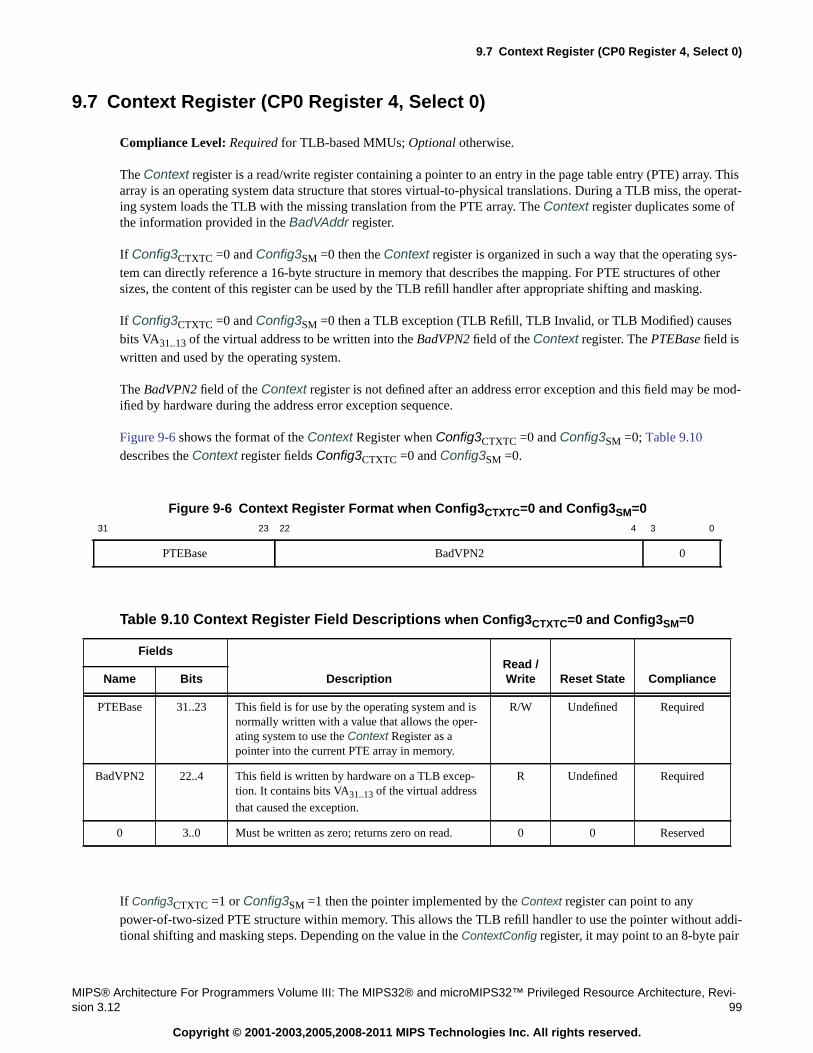
9.7 Context Register (CP0 Register 4, Select 0)
MIPS® Architecture For Programmers Volume III: The MIPS32® and microMIPS32™ Privileged Resource Architecture, Revi-sion 3.12 99
Copyright © 2001-2003,2005,2008-2011 MIPS Technologies Inc. All rights reserved.
9.7 Context Register (CP0 Register 4, Select 0)
Compliance Level: Required for TLB-based MMUs; Optional otherwise.
The Context register is a read/write register containing a pointer to an entry in the page table entry (PTE) array. Thisarray is an operating system data structure that stores virtual-to-physical translations. During a TLB miss, the operat-ing system loads the TLB with the missing translation from the PTE array. The Context register duplicates some ofthe information provided in the BadVAddr register.
If Config3CTXTC =0 and Config3SM =0 then the Context register is organized in such a way that the operating sys-tem can directly reference a 16-byte structure in memory that describes the mapping. For PTE structures of othersizes, the content of this register can be used by the TLB refill handler after appropriate shifting and masking.
If Config3CTXTC =0 and Config3SM =0 then a TLB exception (TLB Refill, TLB Invalid, or TLB Modified) causesbits VA31..13 of the virtual address to be written into the BadVPN2 field of the Context register. The PTEBase field iswritten and used by the operating system.
The BadVPN2 field of the Context register is not defined after an address error exception and this field may be mod-ified by hardware during the address error exception sequence.
Figure 9-6 shows the format of the Context Register when Config3CTXTC =0 and Config3SM =0; Table 9.10describes the Context register fields Config3CTXTC =0 and Config3SM =0.
If Config3CTXTC =1 or Config3SM =1 then the pointer implemented by the Context register can point to anypower-of-two-sized PTE structure within memory. This allows the TLB refill handler to use the pointer without addi-tional shifting and masking steps. Depending on the value in the ContextConfig register, it may point to an 8-byte pair
Figure 9-6 Context Register Format when Config3CTXTC=0 and Config3SM=031 23 22 4 3 0
PTEBase BadVPN2 0
Table 9.10 Context Register Field Descriptions when Config3CTXTC=0 and Config3SM=0
Fields
DescriptionRead /Write Reset State ComplianceName Bits
PTEBase 31..23 This field is for use by the operating system and isnormally written with a value that allows the oper-ating system to use the Context Register as apointer into the current PTE array in memory.
R/W Undefined Required
BadVPN2 22..4 This field is written by hardware on a TLB excep-tion. It contains bits VA31..13 of the virtual address
that caused the exception.
R Undefined Required
0 3..0 Must be written as zero; returns zero on read. 0 0 Reserved
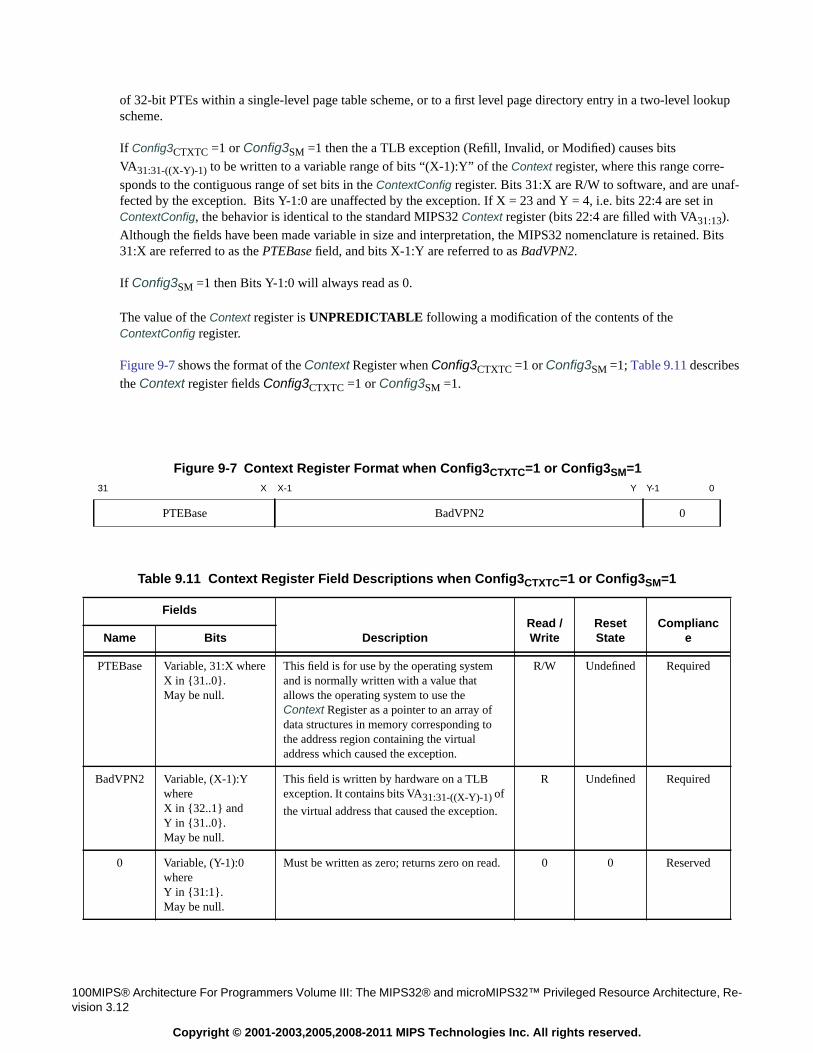
100MIPS® Architecture For Programmers Volume III: The MIPS32® and microMIPS32™ Privileged Resource Architecture, Re-vision 3.12
Copyright © 2001-2003,2005,2008-2011 MIPS Technologies Inc. All rights reserved.
of 32-bit PTEs within a single-level page table scheme, or to a first level page directory entry in a two-level lookupscheme.
If Config3CTXTC =1 or Config3SM =1 then the a TLB exception (Refill, Invalid, or Modified) causes bitsVA31:31-((X-Y)-1) to be written to a variable range of bits “(X-1):Y” of the Context register, where this range corre-sponds to the contiguous range of set bits in the ContextConfig register. Bits 31:X are R/W to software, and are unaf-fected by the exception. Bits Y-1:0 are unaffected by the exception. If X = 23 and Y = 4, i.e. bits 22:4 are set inContextConfig, the behavior is identical to the standard MIPS32 Context register (bits 22:4 are filled with VA31:13).Although the fields have been made variable in size and interpretation, the MIPS32 nomenclature is retained. Bits31:X are referred to as the PTEBase field, and bits X-1:Y are referred to as BadVPN2.
If Config3SM =1 then Bits Y-1:0 will always read as 0.
The value of the Context register is UNPREDICTABLE following a modification of the contents of theContextConfig register.
Figure 9-7 shows the format of the Context Register when Config3CTXTC =1 or Config3SM =1; Table 9.11 describesthe Context register fields Config3CTXTC =1 or Config3SM =1.
Figure 9-7 Context Register Format when Config3CTXTC=1 or Config3SM=131 X X-1 Y Y-1 0
PTEBase BadVPN2 0
Table 9.11 Context Register Field Descriptions when Config3CTXTC=1 or Config3SM=1
Fields
DescriptionRead /Write
ResetState
ComplianceName Bits
PTEBase Variable, 31:X whereX in {31..0}.May be null.
This field is for use by the operating systemand is normally written with a value thatallows the operating system to use theContext Register as a pointer to an array ofdata structures in memory corresponding tothe address region containing the virtualaddress which caused the exception.
R/W Undefined Required
BadVPN2 Variable, (X-1):YwhereX in {32..1} andY in {31..0}.May be null.
This field is written by hardware on a TLBexception. It contains bits VA31:31-((X-Y)-1) of
the virtual address that caused the exception.
R Undefined Required
0 Variable, (Y-1):0whereY in {31:1}.May be null.
Must be written as zero; returns zero on read. 0 0 Reserved
9.7 Context Register (CP0 Register 4, Select 0)
MIPS® Architecture For Programmers Volume III: The MIPS32® and microMIPS32™ Privileged Resource Architecture, Revi-sion 3.12 101
Copyright © 2001-2003,2005,2008-2011 MIPS Technologies Inc. All rights reserved.

102MIPS® Architecture For Programmers Volume III: The MIPS32® and microMIPS32™ Privileged Resource Architecture, Re-vision 3.12
Copyright © 2001-2003,2005,2008-2011 MIPS Technologies Inc. All rights reserved.
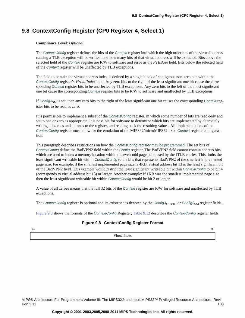
9.8 ContextConfig Register (CP0 Register 4, Select 1)
MIPS® Architecture For Programmers Volume III: The MIPS32® and microMIPS32™ Privileged Resource Architecture, Revi-sion 3.12 103
Copyright © 2001-2003,2005,2008-2011 MIPS Technologies Inc. All rights reserved.
9.8 ContextConfig Register (CP0 Register 4, Select 1)
Compliance Level: Optional.
The ContextConfig register defines the bits of the Context register into which the high order bits of the virtual addresscausing a TLB exception will be written, and how many bits of that virtual address will be extracted. Bits above theselected field of the Context register are R/W to software and serve as the PTEBase field. Bits below the selected fieldof the Context register will be unaffected by TLB exceptions.
The field to contain the virtual address index is defined by a single block of contiguous non-zero bits within theContextConfig register’s VirtualIndex field. Any zero bits to the right of the least significant one bit cause the corre-sponding Context register bits to be unaffected by TLB exceptions. Any zero bits to the left of the most significantone bit cause the corresponding Context register bits to be R/W to software and unaffected by TLB exceptions.
If Config3SM is set, then any zero bits to the right of the least significant one bit causes the corresponding Context reg-ister bits to be read as zero.
It is permissible to implement a subset of the ContextConfig register, in which some number of bits are read-only andset to one or zero as appropriate. It is possible for software to determine which bits are implemented by alternatelywriting all zeroes and all ones to the register, and reading back the resulting values. All implementations of theContextConfig register must allow for the emulation of the MIPS32/microMIPS32 fixed Context register configura-tion.
This paragraph describes restrictions on how the ContextConfig register may be programmed. The set bits ofContextConfig define the BadVPN2 field within the Config register. The BadVPN2 field cannot contain address bitswhich are used to index a memory location within the even-odd page pairs used by the JTLB entries. This limits theleast significant writeable bit within ContextConfig to the bits that represents BadVPN2 of the smallest implementedpage size. For example, if the smallest implemented page size is 4KB, virtual address bit 13 is the least significant bitof the BadVPN2 field. This example would restrict the least significant writeable bit within ContextConfig to be bit 4(corresponds to virtual address bit 13) or larger. Another example: if 1KB was the smallest implemented page sizethen the least significant writeable bit within ContextConfig would be bit 2 or larger.
A value of all zeroes means that the full 32 bits of the Context register are R/W for software and unaffected by TLBexceptions.
The ContextConfig register is optional and its existence is denoted by the Config3CTXTC or Config3SM register fields.
Figure 9.8 shows the formats of the ContextConfig Register; Table 9.12 describes the ContextConfig register fields.
Figure 9.8 ContextConfig Register Format31 0
VirtualIndex
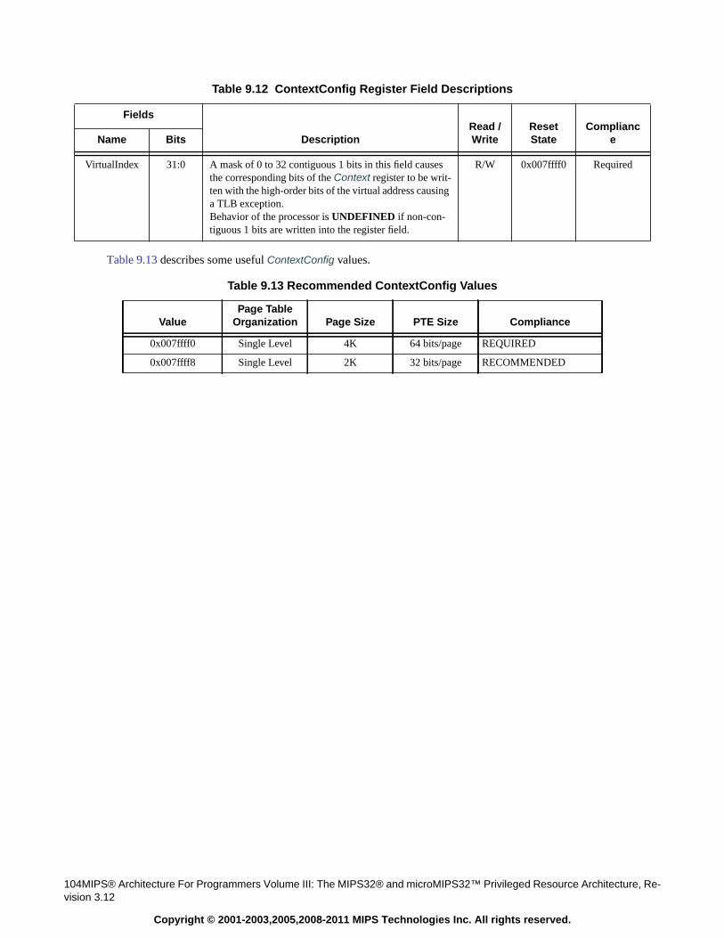
104MIPS® Architecture For Programmers Volume III: The MIPS32® and microMIPS32™ Privileged Resource Architecture, Re-vision 3.12
Copyright © 2001-2003,2005,2008-2011 MIPS Technologies Inc. All rights reserved.
Table 9.13 describes some useful ContextConfig values.
Table 9.12 ContextConfig Register Field Descriptions
Fields
DescriptionRead /Write
ResetState
ComplianceName Bits
VirtualIndex 31:0 A mask of 0 to 32 contiguous 1 bits in this field causesthe corresponding bits of the Context register to be writ-ten with the high-order bits of the virtual address causinga TLB exception.Behavior of the processor is UNDEFINED if non-con-tiguous 1 bits are written into the register field.
R/W 0x007ffff0 Required
Table 9.13 Recommended ContextConfig Values
ValuePage Table
Organization Page Size PTE Size Compliance
0x007ffff0 Single Level 4K 64 bits/page REQUIRED
0x007ffff8 Single Level 2K 32 bits/page RECOMMENDED
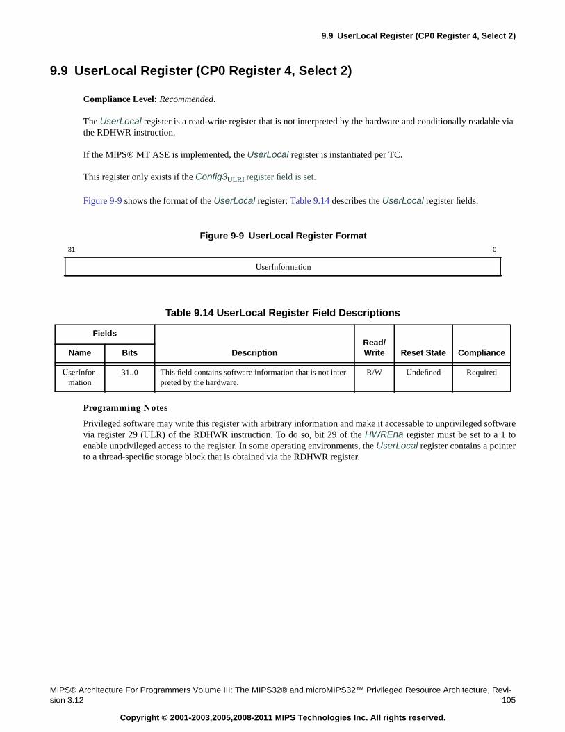
9.9 UserLocal Register (CP0 Register 4, Select 2)
MIPS® Architecture For Programmers Volume III: The MIPS32® and microMIPS32™ Privileged Resource Architecture, Revi-sion 3.12 105
Copyright © 2001-2003,2005,2008-2011 MIPS Technologies Inc. All rights reserved.
9.9 UserLocal Register (CP0 Register 4, Select 2)
Compliance Level: Recommended.
The UserLocal register is a read-write register that is not interpreted by the hardware and conditionally readable viathe RDHWR instruction.
If the MIPS® MT ASE is implemented, the UserLocal register is instantiated per TC.
This register only exists if the Config3ULRI register field is set.
Figure 9-9 shows the format of the UserLocal register; Table 9.14 describes the UserLocal register fields.
Programming Notes
Privileged software may write this register with arbitrary information and make it accessable to unprivileged softwarevia register 29 (ULR) of the RDHWR instruction. To do so, bit 29 of the HWREna register must be set to a 1 toenable unprivileged access to the register. In some operating environments, the UserLocal register contains a pointerto a thread-specific storage block that is obtained via the RDHWR register.
Figure 9-9 UserLocal Register Format31 0
UserInformation
Table 9.14 UserLocal Register Field Descriptions
Fields
DescriptionRead/Write Reset State ComplianceName Bits
UserInfor-mation
31..0 This field contains software information that is not inter-preted by the hardware.
R/W Undefined Required
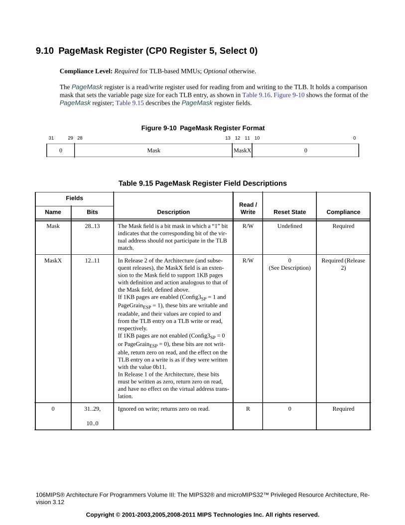
106MIPS® Architecture For Programmers Volume III: The MIPS32® and microMIPS32™ Privileged Resource Architecture, Re-vision 3.12
Copyright © 2001-2003,2005,2008-2011 MIPS Technologies Inc. All rights reserved.
9.10 PageMask Register (CP0 Register 5, Select 0)
Compliance Level: Required for TLB-based MMUs; Optional otherwise.
The PageMask register is a read/write register used for reading from and writing to the TLB. It holds a comparisonmask that sets the variable page size for each TLB entry, as shown in Table 9.16. Figure 9-10 shows the format of thePageMask register; Table 9.15 describes the PageMask register fields.
Figure 9-10 PageMask Register Format31 29 28 13 12 11 10 0
0 Mask MaskX 0
Table 9.15 PageMask Register Field Descriptions
Fields
DescriptionRead /Write Reset State ComplianceName Bits
Mask 28..13 The Mask field is a bit mask in which a “1” bitindicates that the corresponding bit of the vir-tual address should not participate in the TLBmatch.
R/W Undefined Required
MaskX 12..11 In Release 2 of the Architecture (and subse-quent releases), the MaskX field is an exten-sion to the Mask field to support 1KB pageswith definition and action analogous to that ofthe Mask field, defined above.If 1KB pages are enabled (Config3SP = 1 and
PageGrainESP = 1), these bits are writable and
readable, and their values are copied to andfrom the TLB entry on a TLB write or read,respectively.If 1KB pages are not enabled (Config3SP = 0
or PageGrainESP = 0), these bits are not writ-
able, return zero on read, and the effect on theTLB entry on a write is as if they were writtenwith the value 0b11.In Release 1 of the Architecture, these bitsmust be written as zero, return zero on read,and have no effect on the virtual address trans-lation.
R/W 0(See Description)
Required (Release2)
0 31..29,
10..0
Ignored on write; returns zero on read. R 0 Required
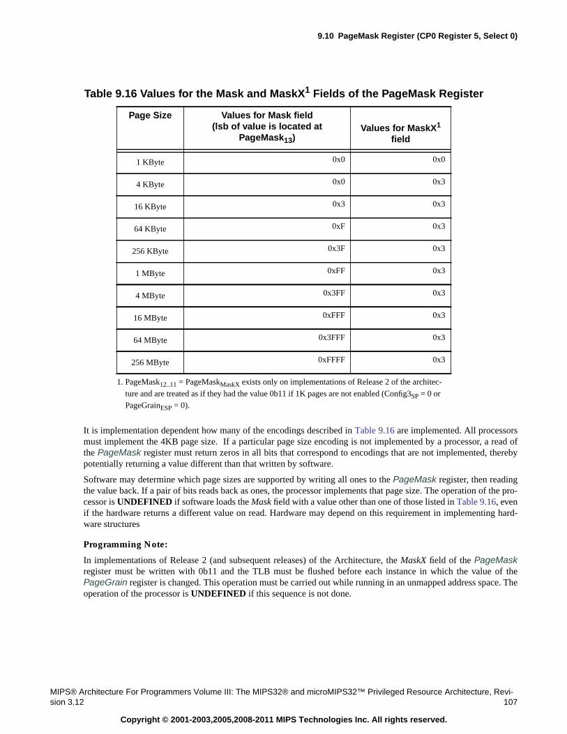
9.10 PageMask Register (CP0 Register 5, Select 0)
MIPS® Architecture For Programmers Volume III: The MIPS32® and microMIPS32™ Privileged Resource Architecture, Revi-sion 3.12 107
Copyright © 2001-2003,2005,2008-2011 MIPS Technologies Inc. All rights reserved.
It is implementation dependent how many of the encodings described in Table 9.16 are implemented. All processorsmust implement the 4KB page size. If a particular page size encoding is not implemented by a processor, a read ofthe PageMask register must return zeros in all bits that correspond to encodings that are not implemented, therebypotentially returning a value different than that written by software.
Software may determine which page sizes are supported by writing all ones to the PageMask register, then readingthe value back. If a pair of bits reads back as ones, the processor implements that page size. The operation of the pro-cessor is UNDEFINED if software loads the Mask field with a value other than one of those listed in Table 9.16, evenif the hardware returns a different value on read. Hardware may depend on this requirement in implementing hard-ware structures
Programming Note:
In implementations of Release 2 (and subsequent releases) of the Architecture, the MaskX field of the PageMaskregister must be written with 0b11 and the TLB must be flushed before each instance in which the value of thePageGrain register is changed. This operation must be carried out while running in an unmapped address space. Theoperation of the processor is UNDEFINED if this sequence is not done.
Table 9.16 Values for the Mask and MaskX1 Fields of the PageMask Register
Page Size Values for Mask field(lsb of value is located at
PageMask13)Values for MaskX1
field
1. PageMask12..11 = PageMaskMaskX exists only on implementations of Release 2 of the architec-
ture and are treated as if they had the value 0b11 if 1K pages are not enabled (Config3SP = 0 or
PageGrainESP = 0).
1 KByte 0x0 0x0
4 KByte 0x0 0x3
16 KByte 0x3 0x3
64 KByte 0xF 0x3
256 KByte 0x3F 0x3
1 MByte 0xFF 0x3
4 MByte 0x3FF 0x3
16 MByte 0xFFF 0x3
64 MByte 0x3FFF 0x3
256 MByte 0xFFFF 0x3
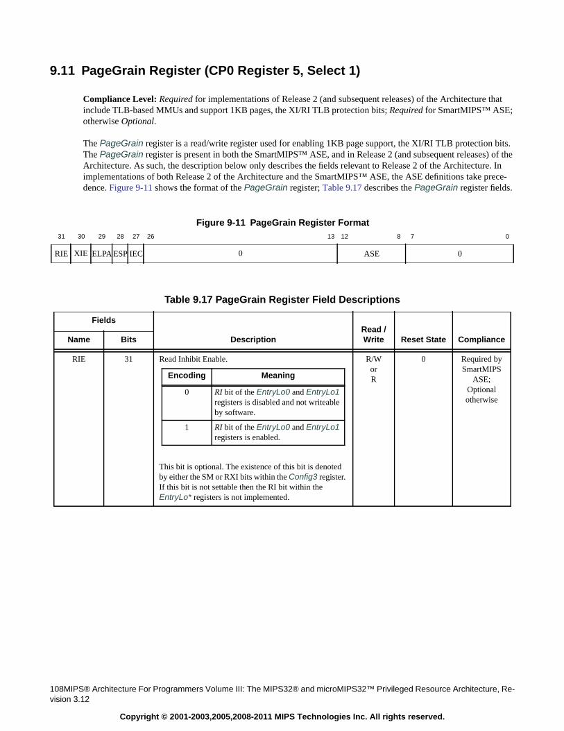
108MIPS® Architecture For Programmers Volume III: The MIPS32® and microMIPS32™ Privileged Resource Architecture, Re-vision 3.12
Copyright © 2001-2003,2005,2008-2011 MIPS Technologies Inc. All rights reserved.
9.11 PageGrain Register (CP0 Register 5, Select 1)
Compliance Level: Required for implementations of Release 2 (and subsequent releases) of the Architecture thatinclude TLB-based MMUs and support 1KB pages, the XI/RI TLB protection bits; Required for SmartMIPS™ ASE;otherwise Optional.
The PageGrain register is a read/write register used for enabling 1KB page support, the XI/RI TLB protection bits.The PageGrain register is present in both the SmartMIPS™ ASE, and in Release 2 (and subsequent releases) of theArchitecture. As such, the description below only describes the fields relevant to Release 2 of the Architecture. Inimplementations of both Release 2 of the Architecture and the SmartMIPS™ ASE, the ASE definitions take prece-dence. Figure 9-11 shows the format of the PageGrain register; Table 9.17 describes the PageGrain register fields.
Figure 9-11 PageGrain Register Format31 30 29 28 27 26 13 12 8 7 0
RIE XIE ELPA ESP IEC 0 ASE 0
Table 9.17 PageGrain Register Field Descriptions
Fields
DescriptionRead /Write Reset State ComplianceName Bits
RIE 31 Read Inhibit Enable.
This bit is optional. The existence of this bit is denotedby either the SM or RXI bits within the Config3 register.If this bit is not settable then the RI bit within theEntryLo* registers is not implemented.
R/WorR
0 Required bySmartMIPS
ASE;Optionalotherwise
Encoding Meaning
0 RI bit of the EntryLo0 and EntryLo1registers is disabled and not writeableby software.
1 RI bit of the EntryLo0 and EntryLo1registers is enabled.
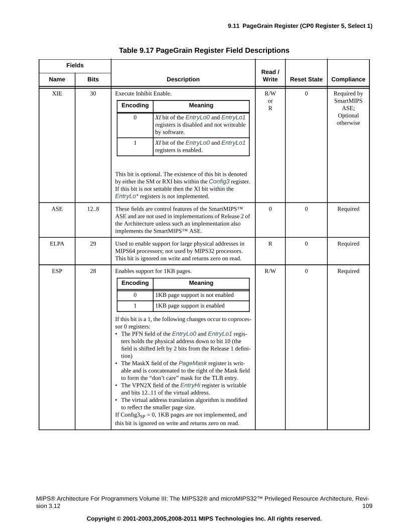
9.11 PageGrain Register (CP0 Register 5, Select 1)
MIPS® Architecture For Programmers Volume III: The MIPS32® and microMIPS32™ Privileged Resource Architecture, Revi-sion 3.12 109
Copyright © 2001-2003,2005,2008-2011 MIPS Technologies Inc. All rights reserved.
XIE 30 Execute Inhibit Enable.
This bit is optional. The existence of this bit is denotedby either the SM or RXI bits within the Config3 register.If this bit is not settable then the XI bit within theEntryLo* registers is not implemented.
R/WorR
0 Required bySmartMIPS
ASE;Optionalotherwise
ASE 12..8 These fields are control features of the SmartMIPS™ASE and are not used in implementations of Release 2 ofthe Architecture unless such an implementation alsoimplements the SmartMIPS™ ASE.
0 0 Required
ELPA 29 Used to enable support for large physical addresses inMIPS64 processors; not used by MIPS32 processors.This bit is ignored on write and returns zero on read.
R 0 Required
ESP 28 Enables support for 1KB pages.
If this bit is a 1, the following changes occur to coproces-sor 0 registers:• The PFN field of the EntryLo0 and EntryLo1 regis-
ters holds the physical address down to bit 10 (thefield is shifted left by 2 bits from the Release 1 defini-tion)
• The MaskX field of the PageMask register is writ-able and is concatenated to the right of the Mask fieldto form the “don’t care” mask for the TLB entry.
• The VPN2X field of the EntryHi register is writableand bits 12..11 of the virtual address.
• The virtual address translation algorithm is modifiedto reflect the smaller page size.
If Config3SP = 0, 1KB pages are not implemented, and
this bit is ignored on write and returns zero on read.
R/W 0 Required
Table 9.17 PageGrain Register Field Descriptions
Fields
DescriptionRead /Write Reset State ComplianceName Bits
Encoding Meaning
0 XI bit of the EntryLo0 and EntryLo1registers is disabled and not writeableby software.
1 XI bit of the EntryLo0 and EntryLo1registers is enabled.
Encoding Meaning
0 1KB page support is not enabled
1 1KB page support is enabled
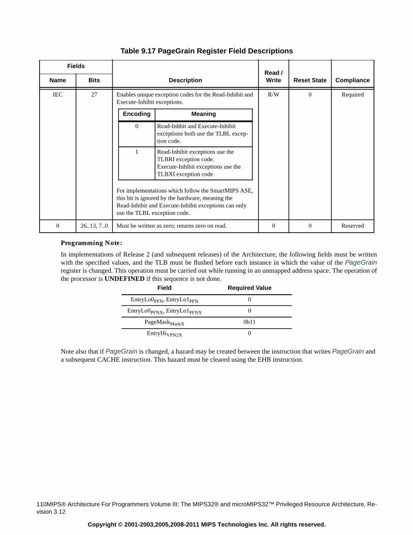
110MIPS® Architecture For Programmers Volume III: The MIPS32® and microMIPS32™ Privileged Resource Architecture, Re-vision 3.12
Copyright © 2001-2003,2005,2008-2011 MIPS Technologies Inc. All rights reserved.
Programming Note:
In implementations of Release 2 (and subsequent releases) of the Architecture, the following fields must be writtenwith the specified values, and the TLB must be flushed before each instance in which the value of the PageGrainregister is changed. This operation must be carried out while running in an unmapped address space. The operation ofthe processor is UNDEFINED if this sequence is not done.
Note also that if PageGrain is changed, a hazard may be created between the instruction that writes PageGrain anda subsequent CACHE instruction. This hazard must be cleared using the EHB instruction.
IEC 27 Enables unique exception codes for the Read-Inhibit andExecute-Inhibit exceptions.
For implementations which follow the SmartMIPS ASE,this bit is ignored by the hardware, meaning theRead-Inhibit and Execute-Inhibit exceptions can onlyuse the TLBL exception code.
R/W 0 Required
0 26..13, 7..0 Must be written as zero; returns zero on read. 0 0 Reserved
Field Required Value
EntryLo0PFN, EntryLo1PFN 0
EntryLo0PFNX, EntryLo1PFNX 0
PageMaskMaskX 0b11
EntryHiVPN2X 0
Table 9.17 PageGrain Register Field Descriptions
Fields
DescriptionRead /Write Reset State ComplianceName Bits
Encoding Meaning
0 Read-Inhbit and Execute-Inhibitexceptions both use the TLBL excep-tion code.
1 Read-Inhibit exceptions use theTLBRI exception code.Execute-Inhibit exceptions use theTLBXI exception code
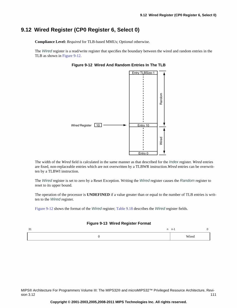
9.12 Wired Register (CP0 Register 6, Select 0)
MIPS® Architecture For Programmers Volume III: The MIPS32® and microMIPS32™ Privileged Resource Architecture, Revi-sion 3.12 111
Copyright © 2001-2003,2005,2008-2011 MIPS Technologies Inc. All rights reserved.
9.12 Wired Register (CP0 Register 6, Select 0)
Compliance Level: Required for TLB-based MMUs; Optional otherwise.
The Wired register is a read/write register that specifies the boundary between the wired and random entries in theTLB as shown in Figure 9-12.
Figure 9-12 Wired And Random Entries In The TLB
The width of the Wired field is calculated in the same manner as that described for the Index register. Wired entriesare fixed, non-replaceable entries which are not overwritten by a TLBWR instruction.Wired entries can be overwrit-ten by a TLBWI instruction.
The Wired register is set to zero by a Reset Exception. Writing the Wired register causes the Random register toreset to its upper bound.
The operation of the processor is UNDEFINED if a value greater than or equal to the number of TLB entries is writ-ten to the Wired register.
Figure 9-12 shows the format of the Wired register; Table 9.18 describes the Wired register fields.
Figure 9-13 Wired Register Format31 n n-1 0
0 Wired
Ran
dom
Wire
d
Entry TLBSize-1
Entry 0
Entry 1010Wired Register
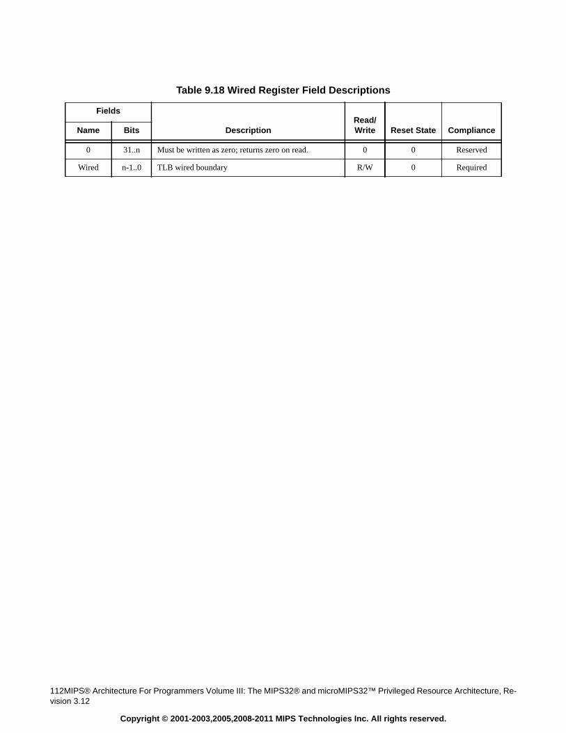
112MIPS® Architecture For Programmers Volume III: The MIPS32® and microMIPS32™ Privileged Resource Architecture, Re-vision 3.12
Copyright © 2001-2003,2005,2008-2011 MIPS Technologies Inc. All rights reserved.
Table 9.18 Wired Register Field Descriptions
Fields
DescriptionRead/Write Reset State ComplianceName Bits
0 31..n Must be written as zero; returns zero on read. 0 0 Reserved
Wired n-1..0 TLB wired boundary R/W 0 Required
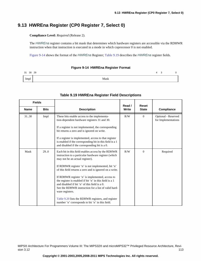
9.13 HWREna Register (CP0 Register 7, Select 0)
MIPS® Architecture For Programmers Volume III: The MIPS32® and microMIPS32™ Privileged Resource Architecture, Revi-sion 3.12 113
Copyright © 2001-2003,2005,2008-2011 MIPS Technologies Inc. All rights reserved.
9.13 HWREna Register (CP0 Register 7, Select 0)
Compliance Level: Required (Release 2).
The HWREna register contains a bit mask that determines which hardware registers are accessible via the RDHWRinstruction when that instruction is executed in a mode in which coprocessor 0 is not enabled.
Figure 9-14 shows the format of the HWREna Register; Table 9.19 describes the HWREna register fields.
Figure 9-14 HWREna Register Format31 30 29 4 3 0
Impl Mask
Table 9.19 HWREna Register Field Descriptions
Fields
DescriptionRead /Write
ResetState ComplianceName Bits
31..30 Impl These bits enable access to the implementa-tion-dependent hardware registers 31 and 30.
If a register is not implemented, the correspondingbit returns a zero and is ignored on write.
If a register is implemented, access to that registeris enabled if the corresponding bit in this field is a 1and disabled if the corresponding bit is a 0.
R/W 0 Optional - Reservedfor Implementations
Mask 29..0 Each bit in this field enables access by the RDHWRinstruction to a particular hardware register (whichmay not be an actual register).
If RDHWR register ‘n’ is not implemented, bit ‘n’of this field returns a zero and is ignored on a write.
If RDHWR register ‘n’ is implemented, access tothe register is enabled if bit ‘n’ in this field is a 1and disabled if bit ‘n’ of this field is a 0.See the RDHWR instruction for a list of valid hard-ware registers.
Table 9.20 lists the RDHWR registers, and registernumber ‘n’ corresponds to bit ‘n’ in this field.
R/W 0 Required
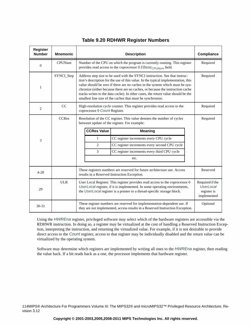
114MIPS® Architecture For Programmers Volume III: The MIPS32® and microMIPS32™ Privileged Resource Architecture, Re-vision 3.12
Copyright © 2001-2003,2005,2008-2011 MIPS Technologies Inc. All rights reserved.
Using the HWREna register, privileged software may select which of the hardware registers are accessible via theRDHWR instruction. In doing so, a register may be virtualized at the cost of handling a Reserved Instruction Excep-tion, interpreting the instruction, and returning the virtualized value. For example, if it is not desirable to providedirect access to the Count register, access to that register may be individually disabled and the return value can bevirtualized by the operating system.
Software may determine which registers are implemented by writing all ones to the HWREna register, then readingthe value back. If a bit reads back as a one, the processor implements that hardware register.
Table 9.20 RDHWR Register Numbers
RegisterNumber Mnemonic Description Compliance
0CPUNum Number of the CPU on which the program is currently running. This register
provides read access to the coprocessor 0 EBaseCPUNum field.Required
1
SYNCI_Step Address step size to be used with the SYNCI instruction. See that instruc-tion’s description for the use of this value. In the typical implementation, thisvalue should be zero if there are no caches in the system which must be syn-chronize (either because there are no caches, or because the instruction cachetracks writes to the data cache). In other cases, the return value should be thesmallest line size of the caches that must be synchronize.
Required
2CC High-resolution cycle counter. This register provides read access to the
coprocessor 0 Count Register.Required
3
CCRes Resolution of the CC register. This value denotes the number of cyclesbetween update of the register. For example:
Required
4-28These registers numbers are reserved for future architecture use. Accessresults in a Reserved Instruction Exception.
Reserved
29
ULR User Local Register. This register provides read access to the coprocessor 0UserLocal register, if it is implemented. In some operating environments,the UserLocal register is a pointer to a thread-specific storage block.
Required if theUserLocalregister is
implemented
30-31These register numbers are reserved for implementation-dependent use. Ifthey are not implemented, access results in a Reserved Instruction Exception.
Optional
CCRes Value Meaning
1 CC register increments every CPU cycle
2 CC register increments every second CPU cycle
3 CC register increments every third CPU cycle
etc.
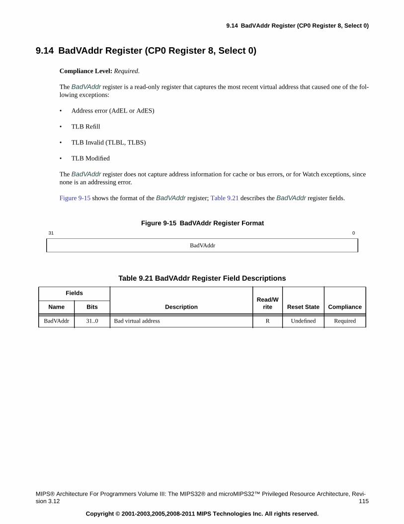
9.14 BadVAddr Register (CP0 Register 8, Select 0)
MIPS® Architecture For Programmers Volume III: The MIPS32® and microMIPS32™ Privileged Resource Architecture, Revi-sion 3.12 115
Copyright © 2001-2003,2005,2008-2011 MIPS Technologies Inc. All rights reserved.
9.14 BadVAddr Register (CP0 Register 8, Select 0)
Compliance Level: Required.
The BadVAddr register is a read-only register that captures the most recent virtual address that caused one of the fol-lowing exceptions:
• Address error (AdEL or AdES)
• TLB Refill
• TLB Invalid (TLBL, TLBS)
• TLB Modified
The BadVAddr register does not capture address information for cache or bus errors, or for Watch exceptions, sincenone is an addressing error.
Figure 9-15 shows the format of the BadVAddr register; Table 9.21 describes the BadVAddr register fields.
Figure 9-15 BadVAddr Register Format31 0
BadVAddr
Table 9.21 BadVAddr Register Field Descriptions
Fields
DescriptionRead/W
rite Reset State ComplianceName Bits
BadVAddr 31..0 Bad virtual address R Undefined Required
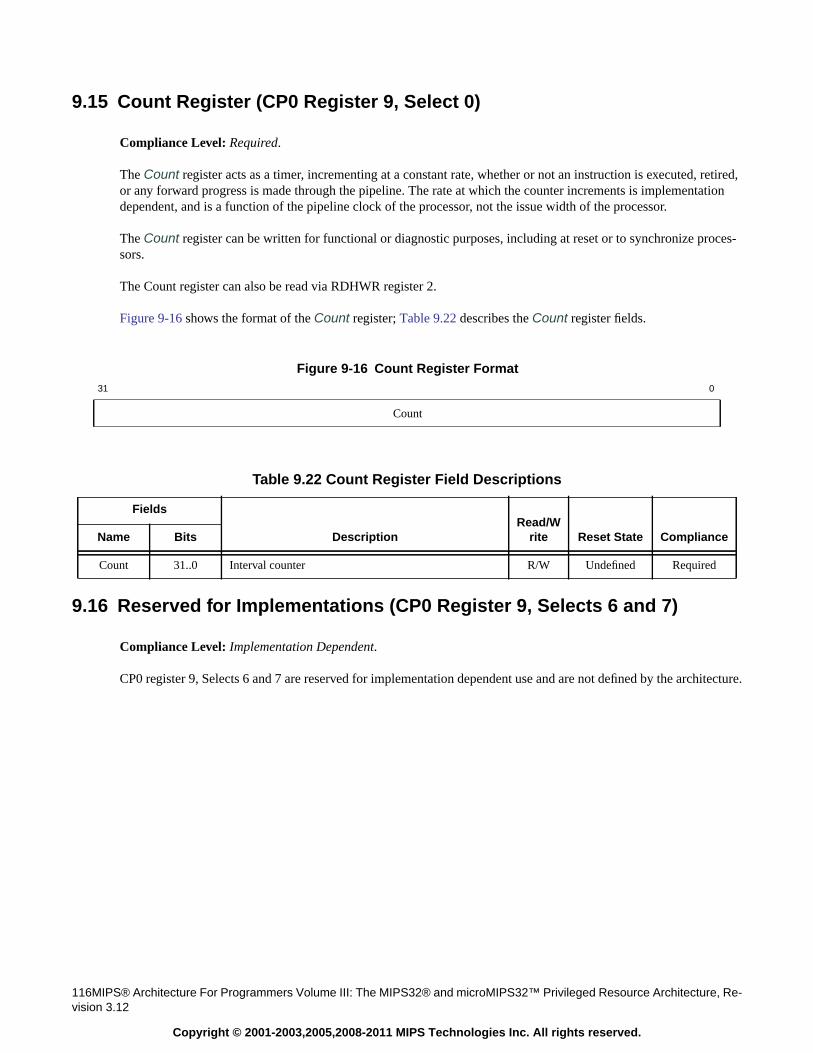
116MIPS® Architecture For Programmers Volume III: The MIPS32® and microMIPS32™ Privileged Resource Architecture, Re-vision 3.12
Copyright © 2001-2003,2005,2008-2011 MIPS Technologies Inc. All rights reserved.
9.15 Count Register (CP0 Register 9, Select 0)
Compliance Level: Required.
The Count register acts as a timer, incrementing at a constant rate, whether or not an instruction is executed, retired,or any forward progress is made through the pipeline. The rate at which the counter increments is implementationdependent, and is a function of the pipeline clock of the processor, not the issue width of the processor.
The Count register can be written for functional or diagnostic purposes, including at reset or to synchronize proces-sors.
The Count register can also be read via RDHWR register 2.
Figure 9-16 shows the format of the Count register; Table 9.22 describes the Count register fields.
9.16 Reserved for Implementations (CP0 Register 9, Selects 6 and 7)
Compliance Level: Implementation Dependent.
CP0 register 9, Selects 6 and 7 are reserved for implementation dependent use and are not defined by the architecture.
Figure 9-16 Count Register Format31 0
Count
Table 9.22 Count Register Field Descriptions
Fields
DescriptionRead/W
rite Reset State ComplianceName Bits
Count 31..0 Interval counter R/W Undefined Required
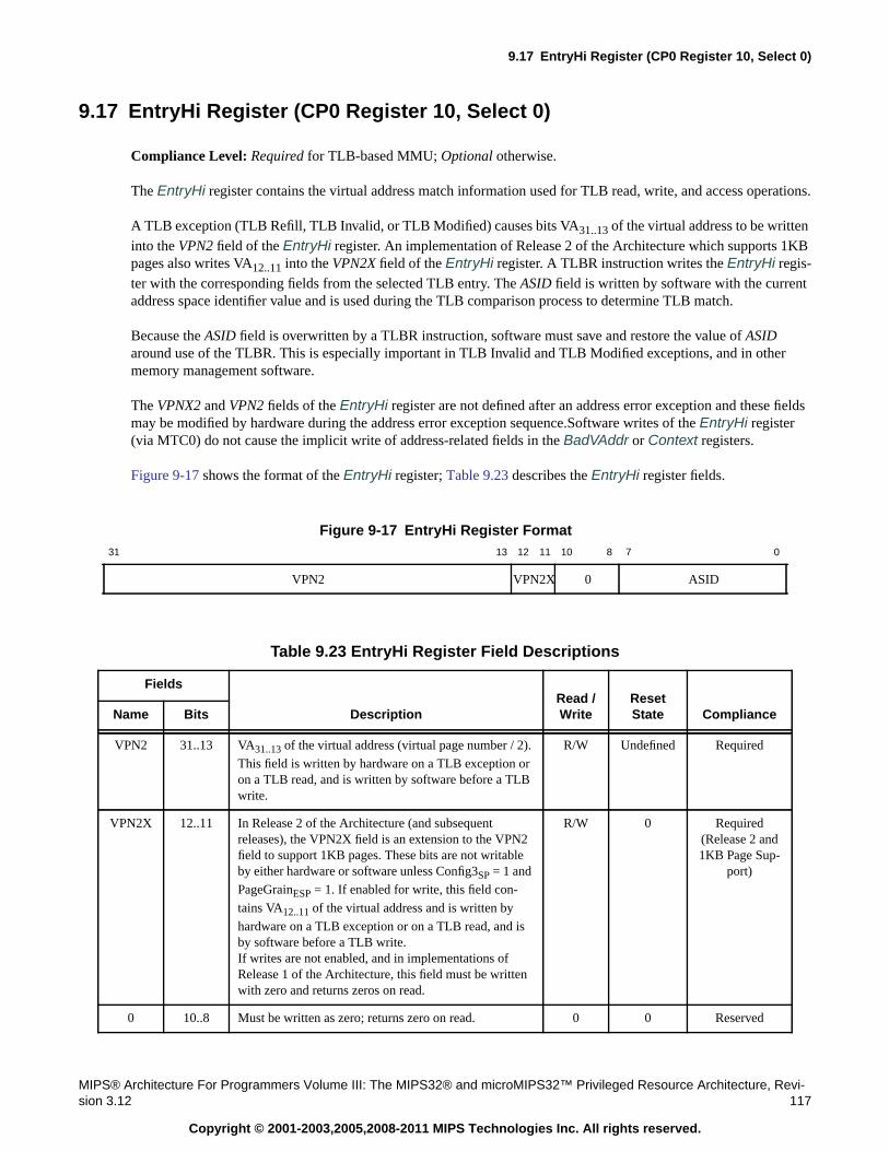
9.17 EntryHi Register (CP0 Register 10, Select 0)
MIPS® Architecture For Programmers Volume III: The MIPS32® and microMIPS32™ Privileged Resource Architecture, Revi-sion 3.12 117
Copyright © 2001-2003,2005,2008-2011 MIPS Technologies Inc. All rights reserved.
9.17 EntryHi Register (CP0 Register 10, Select 0)
Compliance Level: Required for TLB-based MMU; Optional otherwise.
The EntryHi register contains the virtual address match information used for TLB read, write, and access operations.
A TLB exception (TLB Refill, TLB Invalid, or TLB Modified) causes bits VA31..13 of the virtual address to be writteninto the VPN2 field of the EntryHi register. An implementation of Release 2 of the Architecture which supports 1KBpages also writes VA12..11 into the VPN2X field of the EntryHi register. A TLBR instruction writes the EntryHi regis-ter with the corresponding fields from the selected TLB entry. The ASID field is written by software with the currentaddress space identifier value and is used during the TLB comparison process to determine TLB match.
Because the ASID field is overwritten by a TLBR instruction, software must save and restore the value of ASIDaround use of the TLBR. This is especially important in TLB Invalid and TLB Modified exceptions, and in othermemory management software.
The VPNX2 and VPN2 fields of the EntryHi register are not defined after an address error exception and these fieldsmay be modified by hardware during the address error exception sequence.Software writes of the EntryHi register(via MTC0) do not cause the implicit write of address-related fields in the BadVAddr or Context registers.
Figure 9-17 shows the format of the EntryHi register; Table 9.23 describes the EntryHi register fields.
Figure 9-17 EntryHi Register Format31 13 12 11 10 8 7 0
VPN2 VPN2X 0 ASID
Table 9.23 EntryHi Register Field Descriptions
Fields
DescriptionRead /Write
ResetState ComplianceName Bits
VPN2 31..13 VA31..13 of the virtual address (virtual page number / 2).
This field is written by hardware on a TLB exception oron a TLB read, and is written by software before a TLBwrite.
R/W Undefined Required
VPN2X 12..11 In Release 2 of the Architecture (and subsequentreleases), the VPN2X field is an extension to the VPN2field to support 1KB pages. These bits are not writableby either hardware or software unless Config3SP = 1 and
PageGrainESP = 1. If enabled for write, this field con-
tains VA12..11 of the virtual address and is written by
hardware on a TLB exception or on a TLB read, and isby software before a TLB write.If writes are not enabled, and in implementations ofRelease 1 of the Architecture, this field must be writtenwith zero and returns zeros on read.
R/W 0 Required(Release 2 and1KB Page Sup-
port)
0 10..8 Must be written as zero; returns zero on read. 0 0 Reserved
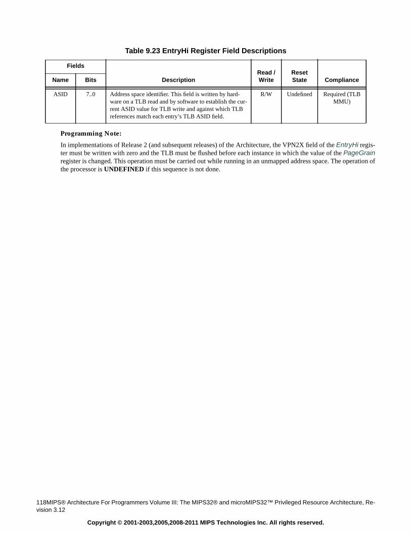
118MIPS® Architecture For Programmers Volume III: The MIPS32® and microMIPS32™ Privileged Resource Architecture, Re-vision 3.12
Copyright © 2001-2003,2005,2008-2011 MIPS Technologies Inc. All rights reserved.
Programming Note:
In implementations of Release 2 (and subsequent releases) of the Architecture, the VPN2X field of the EntryHi regis-ter must be written with zero and the TLB must be flushed before each instance in which the value of the PageGrainregister is changed. This operation must be carried out while running in an unmapped address space. The operation ofthe processor is UNDEFINED if this sequence is not done.
ASID 7..0 Address space identifier. This field is written by hard-ware on a TLB read and by software to establish the cur-rent ASID value for TLB write and against which TLBreferences match each entry’s TLB ASID field.
R/W Undefined Required (TLBMMU)
Table 9.23 EntryHi Register Field Descriptions
Fields
DescriptionRead /Write
ResetState ComplianceName Bits
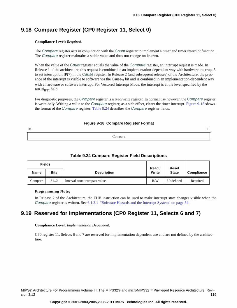
9.18 Compare Register (CP0 Register 11, Select 0)
MIPS® Architecture For Programmers Volume III: The MIPS32® and microMIPS32™ Privileged Resource Architecture, Revi-sion 3.12 119
Copyright © 2001-2003,2005,2008-2011 MIPS Technologies Inc. All rights reserved.
9.18 Compare Register (CP0 Register 11, Select 0)
Compliance Level: Required.
The Compare register acts in conjunction with the Count register to implement a timer and timer interrupt function.The Compare register maintains a stable value and does not change on its own.
When the value of the Count register equals the value of the Compare register, an interrupt request is made. InRelease 1 of the architecture, this request is combined in an implementation-dependent way with hardware interrupt 5to set interrupt bit IP(7) in the Cause register. In Release 2 (and subsequent releases) of the Architecture, the pres-ence of the interrupt is visible to software via the CauseTI bit and is combined in an implementation-dependent waywith a hardware or software interrupt. For Vectored Interrupt Mode, the interrupt is at the level specified by theIntCtlIPTI field.
For diagnostic purposes, the Compare register is a read/write register. In normal use however, the Compare registeris write-only. Writing a value to the Compare register, as a side effect, clears the timer interrupt. Figure 9-18 showsthe format of the Compare register; Table 9.24 describes the Compare register fields.
Programming Note:
In Release 2 of the Architecture, the EHB instruction can be used to make interrupt state changes visible when theCompare register is written. See 6.1.2.1 “Software Hazards and the Interrupt System” on page 54.
9.19 Reserved for Implementations (CP0 Register 11, Selects 6 and 7)
Compliance Level: Implementation Dependent.
CP0 register 11, Selects 6 and 7 are reserved for implementation dependent use and are not defined by the architec-ture.
Figure 9-18 Compare Register Format31 0
Compare
Table 9.24 Compare Register Field Descriptions
Fields
DescriptionRead /Write
ResetState ComplianceName Bits
Compare 31..0 Interval count compare value R/W Undefined Required
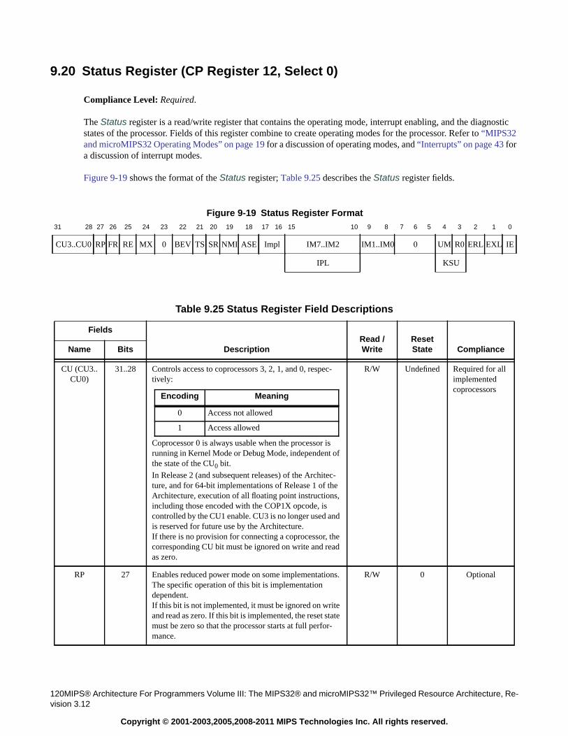
120MIPS® Architecture For Programmers Volume III: The MIPS32® and microMIPS32™ Privileged Resource Architecture, Re-vision 3.12
Copyright © 2001-2003,2005,2008-2011 MIPS Technologies Inc. All rights reserved.
9.20 Status Register (CP Register 12, Select 0)
Compliance Level: Required.
The Status register is a read/write register that contains the operating mode, interrupt enabling, and the diagnosticstates of the processor. Fields of this register combine to create operating modes for the processor. Refer to “MIPS32and microMIPS32 Operating Modes” on page 19 for a discussion of operating modes, and “Interrupts” on page 43 fora discussion of interrupt modes.
Figure 9-19 shows the format of the Status register; Table 9.25 describes the Status register fields.
Figure 9-19 Status Register Format31 28 27 26 25 24 23 22 21 20 19 18 17 16 15 10 9 8 7 6 5 4 3 2 1 0
CU3..CU0 RP FR RE MX 0 BEV TS SR NMI ASE Impl IM7..IM2 IM1..IM0 0 UM R0 ERL EXL IE
IPL KSU
Table 9.25 Status Register Field Descriptions
Fields
DescriptionRead /Write
ResetState ComplianceName Bits
CU (CU3..CU0)
31..28 Controls access to coprocessors 3, 2, 1, and 0, respec-tively:
Coprocessor 0 is always usable when the processor isrunning in Kernel Mode or Debug Mode, independent ofthe state of the CU0 bit.
In Release 2 (and subsequent releases) of the Architec-ture, and for 64-bit implementations of Release 1 of theArchitecture, execution of all floating point instructions,including those encoded with the COP1X opcode, iscontrolled by the CU1 enable. CU3 is no longer used andis reserved for future use by the Architecture.If there is no provision for connecting a coprocessor, thecorresponding CU bit must be ignored on write and readas zero.
R/W Undefined Required for allimplementedcoprocessors
RP 27 Enables reduced power mode on some implementations.The specific operation of this bit is implementationdependent.If this bit is not implemented, it must be ignored on writeand read as zero. If this bit is implemented, the reset statemust be zero so that the processor starts at full perfor-mance.
R/W 0 Optional
Encoding Meaning
0 Access not allowed
1 Access allowed
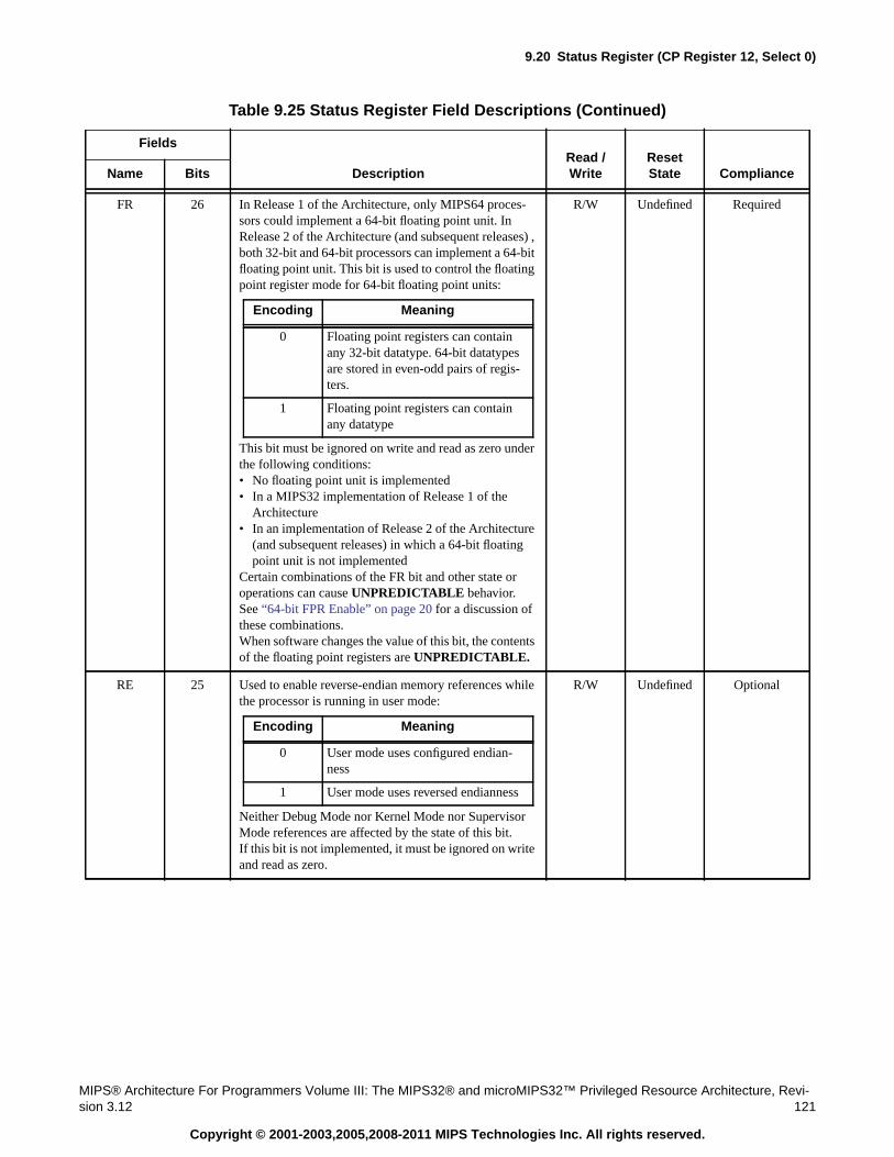
9.20 Status Register (CP Register 12, Select 0)
MIPS® Architecture For Programmers Volume III: The MIPS32® and microMIPS32™ Privileged Resource Architecture, Revi-sion 3.12 121
Copyright © 2001-2003,2005,2008-2011 MIPS Technologies Inc. All rights reserved.
FR 26 In Release 1 of the Architecture, only MIPS64 proces-sors could implement a 64-bit floating point unit. InRelease 2 of the Architecture (and subsequent releases) ,both 32-bit and 64-bit processors can implement a 64-bitfloating point unit. This bit is used to control the floatingpoint register mode for 64-bit floating point units:
This bit must be ignored on write and read as zero underthe following conditions:• No floating point unit is implemented• In a MIPS32 implementation of Release 1 of the
Architecture• In an implementation of Release 2 of the Architecture
(and subsequent releases) in which a 64-bit floatingpoint unit is not implemented
Certain combinations of the FR bit and other state oroperations can cause UNPREDICTABLE behavior.See “64-bit FPR Enable” on page 20 for a discussion ofthese combinations.When software changes the value of this bit, the contentsof the floating point registers are UNPREDICTABLE.
R/W Undefined Required
RE 25 Used to enable reverse-endian memory references whilethe processor is running in user mode:
Neither Debug Mode nor Kernel Mode nor SupervisorMode references are affected by the state of this bit.If this bit is not implemented, it must be ignored on writeand read as zero.
R/W Undefined Optional
Table 9.25 Status Register Field Descriptions (Continued)
Fields
DescriptionRead /Write
ResetState ComplianceName Bits
Encoding Meaning
0 Floating point registers can containany 32-bit datatype. 64-bit datatypesare stored in even-odd pairs of regis-ters.
1 Floating point registers can containany datatype
Encoding Meaning
0 User mode uses configured endian-ness
1 User mode uses reversed endianness
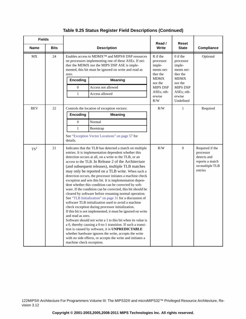
122MIPS® Architecture For Programmers Volume III: The MIPS32® and microMIPS32™ Privileged Resource Architecture, Re-vision 3.12
Copyright © 2001-2003,2005,2008-2011 MIPS Technologies Inc. All rights reserved.
MX 24 Enables access to MDMX™ and MIPS® DSP resourceson processors implementing one of these ASEs. If nei-ther the MDMX nor the MIPS DSP ASE is imple-mented, this bit must be ignored on write and read aszero.
R if theprocessorimple-ments nei-ther theMDMXnor theMIPS DSPASEs; oth-erwiseR/W
0 if theprocessorimple-ments nei-ther theMDMXnor theMIPS DSPASEs; oth-erwiseUndefined
Optional
BEV 22 Controls the location of exception vectors:
See “Exception Vector Locations” on page 57 fordetails.
R/W 1 Required
TS1 21 Indicates that the TLB has detected a match on multipleentries. It is implementation dependent whether thisdetection occurs at all, on a write to the TLB, or anaccess to the TLB. In Release 2 of the Architecture(and subsequent releases), multiple TLB matchesmay only be reported on a TLB write. When such adetection occurs, the processor initiates a machine checkexception and sets this bit. It is implementation depen-dent whether this condition can be corrected by soft-ware. If the condition can be corrected, this bit should becleared by software before resuming normal operation.See “TLB Initialization” on page 31 for a discussion ofsoftware TLB initialization used to avoid a machinecheck exception during processor initialization.If this bit is not implemented, it must be ignored on writeand read as zero.Software should not write a 1 to this bit when its value isa 0, thereby causing a 0-to-1 transition. If such a transi-tion is caused by software, it is UNPREDICTABLEwhether hardware ignores the write, accepts the writewith no side effects, or accepts the write and initiates amachine check exception.
R/W 0 Required if theprocessordetects andreports a matchon multiple TLBentries
Table 9.25 Status Register Field Descriptions (Continued)
Fields
DescriptionRead /Write
ResetState ComplianceName Bits
Encoding Meaning
0 Access not allowed
1 Access allowed
Encoding Meaning
0 Normal
1 Bootstrap
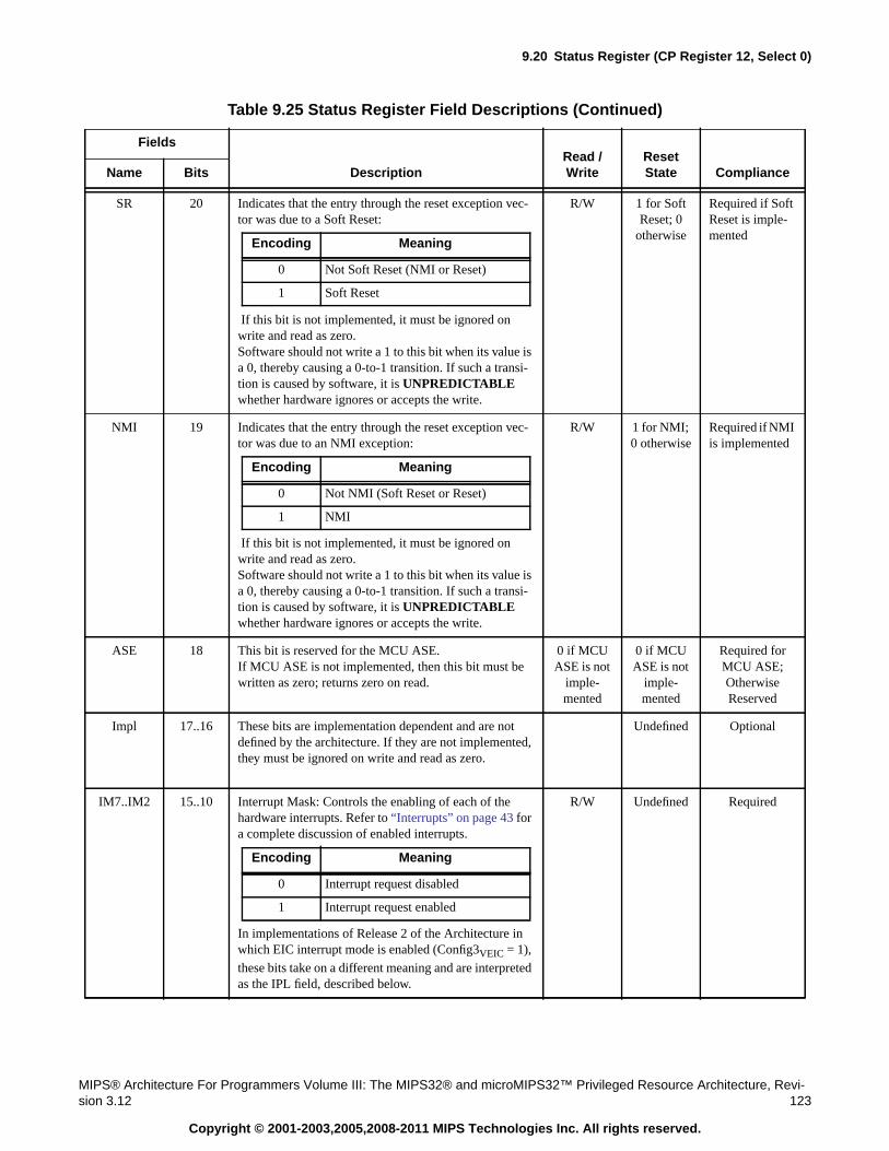
9.20 Status Register (CP Register 12, Select 0)
MIPS® Architecture For Programmers Volume III: The MIPS32® and microMIPS32™ Privileged Resource Architecture, Revi-sion 3.12 123
Copyright © 2001-2003,2005,2008-2011 MIPS Technologies Inc. All rights reserved.
SR 20 Indicates that the entry through the reset exception vec-tor was due to a Soft Reset:
If this bit is not implemented, it must be ignored onwrite and read as zero.Software should not write a 1 to this bit when its value isa 0, thereby causing a 0-to-1 transition. If such a transi-tion is caused by software, it is UNPREDICTABLEwhether hardware ignores or accepts the write.
R/W 1 for SoftReset; 0
otherwise
Required if SoftReset is imple-mented
NMI 19 Indicates that the entry through the reset exception vec-tor was due to an NMI exception:
If this bit is not implemented, it must be ignored onwrite and read as zero.Software should not write a 1 to this bit when its value isa 0, thereby causing a 0-to-1 transition. If such a transi-tion is caused by software, it is UNPREDICTABLEwhether hardware ignores or accepts the write.
R/W 1 for NMI;0 otherwise
Required if NMIis implemented
ASE 18 This bit is reserved for the MCU ASE.If MCU ASE is not implemented, then this bit must bewritten as zero; returns zero on read.
0 if MCUASE is not
imple-mented
0 if MCUASE is not
imple-mented
Required forMCU ASE;OtherwiseReserved
Impl 17..16 These bits are implementation dependent and are notdefined by the architecture. If they are not implemented,they must be ignored on write and read as zero.
Undefined Optional
IM7..IM2 15..10 Interrupt Mask: Controls the enabling of each of thehardware interrupts. Refer to “Interrupts” on page 43 fora complete discussion of enabled interrupts.
In implementations of Release 2 of the Architecture inwhich EIC interrupt mode is enabled (Config3VEIC = 1),
these bits take on a different meaning and are interpretedas the IPL field, described below.
R/W Undefined Required
Table 9.25 Status Register Field Descriptions (Continued)
Fields
DescriptionRead /Write
ResetState ComplianceName Bits
Encoding Meaning
0 Not Soft Reset (NMI or Reset)
1 Soft Reset
Encoding Meaning
0 Not NMI (Soft Reset or Reset)
1 NMI
Encoding Meaning
0 Interrupt request disabled
1 Interrupt request enabled
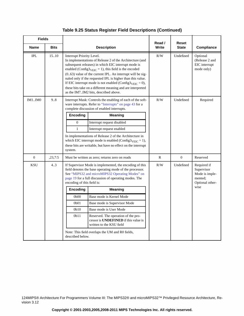
124MIPS® Architecture For Programmers Volume III: The MIPS32® and microMIPS32™ Privileged Resource Architecture, Re-vision 3.12
Copyright © 2001-2003,2005,2008-2011 MIPS Technologies Inc. All rights reserved.
IPL 15..10 Interrupt Priority Level.In implementations of Release 2 of the Architecture (andsubsequent releases) in which EIC interrupt mode isenabled (Config3VEIC = 1), this field is the encoded
(0..63) value of the current IPL. An interrupt will be sig-naled only if the requested IPL is higher than this value.If EIC interrupt mode is not enabled (Config3VEIC = 0),
these bits take on a different meaning and are interpretedas the IM7..IM2 bits, described above.
R/W Undefined Optional(Release 2 andEIC interruptmode only)
IM1..IM0 9..8 Interrupt Mask: Controls the enabling of each of the soft-ware interrupts. Refer to “Interrupts” on page 43 for acomplete discussion of enabled interrupts.
In implementations of Release 2 of the Architecture inwhich EIC interrupt mode is enabled (Config3VEIC = 1),
these bits are writable, but have no effect on the interruptsystem.
R/W Undefined Required
0 ,23,7:5 Must be written as zero; returns zero on reads R 0 Reserved
KSU 4..3 If Supervisor Mode is implemented, the encoding of thisfield denotes the base operating mode of the processor.See “MIPS32 and microMIPS32 Operating Modes” onpage 19 for a full discussion of operating modes. Theencoding of this field is:
Note: This field overlaps the UM and R0 fields,described below.
R/W Undefined Required ifSupervisorMode is imple-mented;Optional other-wise
Table 9.25 Status Register Field Descriptions (Continued)
Fields
DescriptionRead /Write
ResetState ComplianceName Bits
Encoding Meaning
0 Interrupt request disabled
1 Interrupt request enabled
Encoding Meaning
0b00 Base mode is Kernel Mode
0b01 Base mode is Supervisor Mode
0b10 Base mode is User Mode
0b11 Reserved. The operation of the pro-cessor is UNDEFINED if this value iswritten to the KSU field
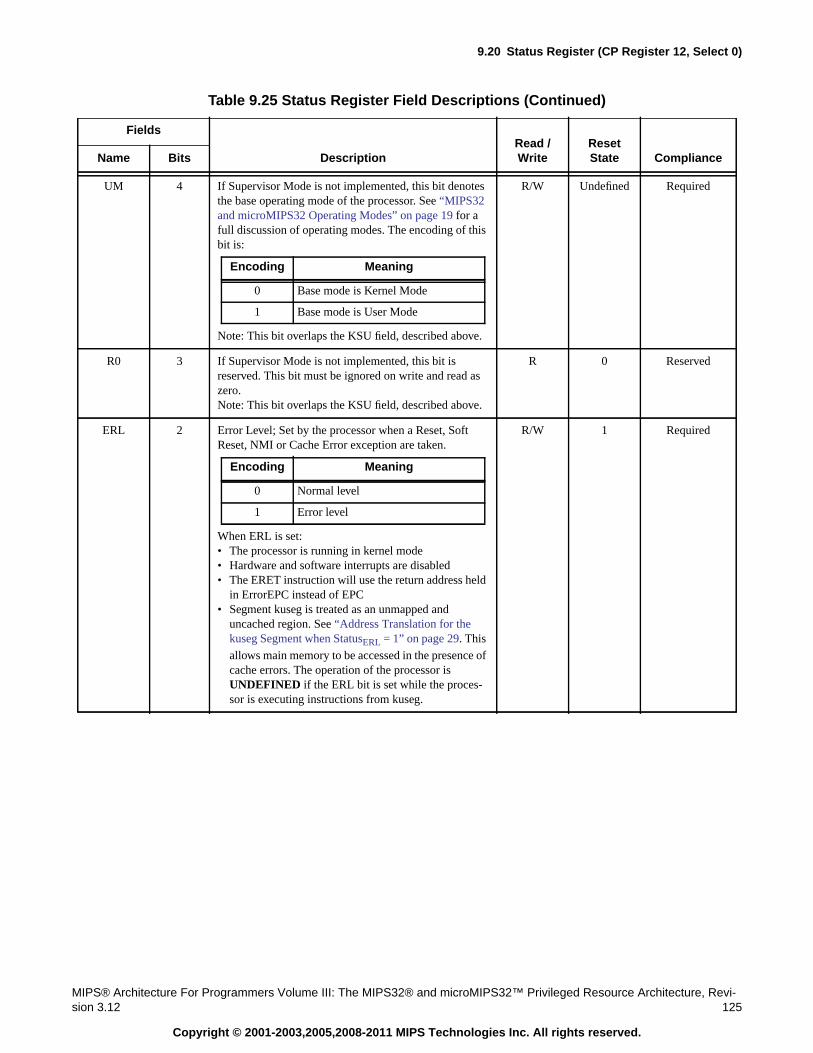
9.20 Status Register (CP Register 12, Select 0)
MIPS® Architecture For Programmers Volume III: The MIPS32® and microMIPS32™ Privileged Resource Architecture, Revi-sion 3.12 125
Copyright © 2001-2003,2005,2008-2011 MIPS Technologies Inc. All rights reserved.
UM 4 If Supervisor Mode is not implemented, this bit denotesthe base operating mode of the processor. See “MIPS32and microMIPS32 Operating Modes” on page 19 for afull discussion of operating modes. The encoding of thisbit is:
Note: This bit overlaps the KSU field, described above.
R/W Undefined Required
R0 3 If Supervisor Mode is not implemented, this bit isreserved. This bit must be ignored on write and read aszero.Note: This bit overlaps the KSU field, described above.
R 0 Reserved
ERL 2 Error Level; Set by the processor when a Reset, SoftReset, NMI or Cache Error exception are taken.
When ERL is set:• The processor is running in kernel mode• Hardware and software interrupts are disabled• The ERET instruction will use the return address held
in ErrorEPC instead of EPC• Segment kuseg is treated as an unmapped and
uncached region. See “Address Translation for thekuseg Segment when StatusERL = 1” on page 29. This
allows main memory to be accessed in the presence ofcache errors. The operation of the processor isUNDEFINED if the ERL bit is set while the proces-sor is executing instructions from kuseg.
R/W 1 Required
Table 9.25 Status Register Field Descriptions (Continued)
Fields
DescriptionRead /Write
ResetState ComplianceName Bits
Encoding Meaning
0 Base mode is Kernel Mode
1 Base mode is User Mode
Encoding Meaning
0 Normal level
1 Error level
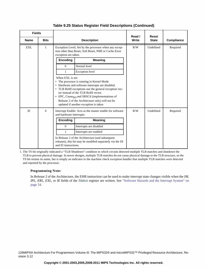
126MIPS® Architecture For Programmers Volume III: The MIPS32® and microMIPS32™ Privileged Resource Architecture, Re-vision 3.12
Copyright © 2001-2003,2005,2008-2011 MIPS Technologies Inc. All rights reserved.
Programming Note:
In Release 2 of the Architecture, the EHB instruction can be used to make interrupt state changes visible when the IM,IPL, ERL, EXL, or IE fields of the Status register are written. See “Software Hazards and the Interrupt System” onpage 54.
EXL 1 Exception Level; Set by the processor when any excep-tion other than Reset, Soft Reset, NMI or Cache Errorexception are taken.
When EXL is set:• The processor is running in Kernel Mode• Hardware and software interrupts are disabled.• TLB Refill exceptions use the general exception vec-
tor instead of the TLB Refill vector.• EPC, CauseBD and SRSCtl (implementations of
Release 2 of the Architecture only) will not beupdated if another exception is taken
R/W Undefined Required
IE 0 Interrupt Enable: Acts as the master enable for softwareand hardware interrupts:
In Release 2 of the Architecture (and subsequentreleases), this bit may be modified separately via the DIand EI instructions.
R/W Undefined Required
1. The TS bit originally indicated a “TLB Shutdown” condition in which circuits detected multiple TLB matches and shutdown theTLB to prevent physical damage. In newer designs, multiple TLB matches do not cause physical damage to the TLB structure, so theTS bit retains its name, but is simply an indicator to the machine check exception handler that multiple TLB matches were detectedand reported by the processor.
Table 9.25 Status Register Field Descriptions (Continued)
Fields
DescriptionRead /Write
ResetState ComplianceName Bits
Encoding Meaning
0 Normal level
1 Exception level
Encoding Meaning
0 Interrupts are disabled
1 Interrupts are enabled
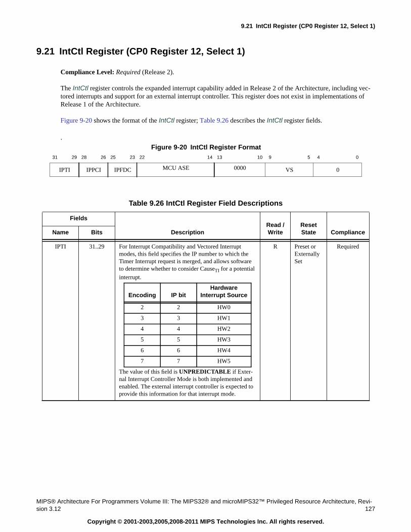
9.21 IntCtl Register (CP0 Register 12, Select 1)
MIPS® Architecture For Programmers Volume III: The MIPS32® and microMIPS32™ Privileged Resource Architecture, Revi-sion 3.12 127
Copyright © 2001-2003,2005,2008-2011 MIPS Technologies Inc. All rights reserved.
9.21 IntCtl Register (CP0 Register 12, Select 1)
Compliance Level: Required (Release 2).
The IntCtl register controls the expanded interrupt capability added in Release 2 of the Architecture, including vec-tored interrupts and support for an external interrupt controller. This register does not exist in implementations ofRelease 1 of the Architecture.
Figure 9-20 shows the format of the IntCtl register; Table 9.26 describes the IntCtl register fields.
.
Figure 9-20 IntCtl Register Format31 29 28 26 25 23 22 14 13 10 9 5 4 0
IPTI IPPCI IPFDC MCU ASE 0000 VS 0
Table 9.26 IntCtl Register Field Descriptions
Fields
DescriptionRead /Write
ResetState ComplianceName Bits
IPTI 31..29 For Interrupt Compatibility and Vectored Interruptmodes, this field specifies the IP number to which theTimer Interrupt request is merged, and allows softwareto determine whether to consider CauseTI for a potential
interrupt.
The value of this field is UNPREDICTABLE if Exter-nal Interrupt Controller Mode is both implemented andenabled. The external interrupt controller is expected toprovide this information for that interrupt mode.
R Preset orExternallySet
Required
Encoding IP bitHardware
Interrupt Source
2 2 HW0
3 3 HW1
4 4 HW2
5 5 HW3
6 6 HW4
7 7 HW5
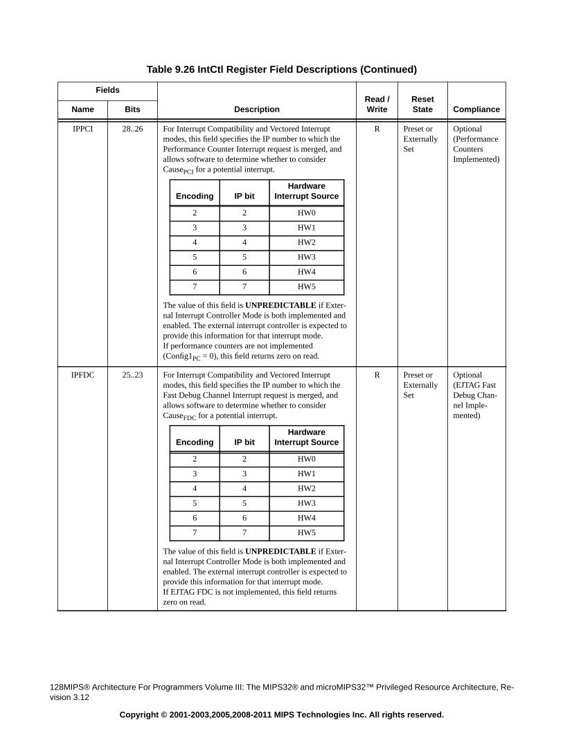
128MIPS® Architecture For Programmers Volume III: The MIPS32® and microMIPS32™ Privileged Resource Architecture, Re-vision 3.12
Copyright © 2001-2003,2005,2008-2011 MIPS Technologies Inc. All rights reserved.
IPPCI 28..26 For Interrupt Compatibility and Vectored Interruptmodes, this field specifies the IP number to which thePerformance Counter Interrupt request is merged, andallows software to determine whether to considerCausePCI for a potential interrupt.
The value of this field is UNPREDICTABLE if Exter-nal Interrupt Controller Mode is both implemented andenabled. The external interrupt controller is expected toprovide this information for that interrupt mode.If performance counters are not implemented(Config1PC = 0), this field returns zero on read.
R Preset orExternallySet
Optional(PerformanceCountersImplemented)
IPFDC 25..23 For Interrupt Compatibility and Vectored Interruptmodes, this field specifies the IP number to which theFast Debug Channel Interrupt request is merged, andallows software to determine whether to considerCauseFDC for a potential interrupt.
The value of this field is UNPREDICTABLE if Exter-nal Interrupt Controller Mode is both implemented andenabled. The external interrupt controller is expected toprovide this information for that interrupt mode.If EJTAG FDC is not implemented, this field returnszero on read.
R Preset orExternallySet
Optional(EJTAG FastDebug Chan-nel Imple-mented)
Table 9.26 IntCtl Register Field Descriptions (Continued)
Fields
DescriptionRead /Write
ResetState ComplianceName Bits
Encoding IP bitHardware
Interrupt Source
2 2 HW0
3 3 HW1
4 4 HW2
5 5 HW3
6 6 HW4
7 7 HW5
Encoding IP bitHardware
Interrupt Source
2 2 HW0
3 3 HW1
4 4 HW2
5 5 HW3
6 6 HW4
7 7 HW5
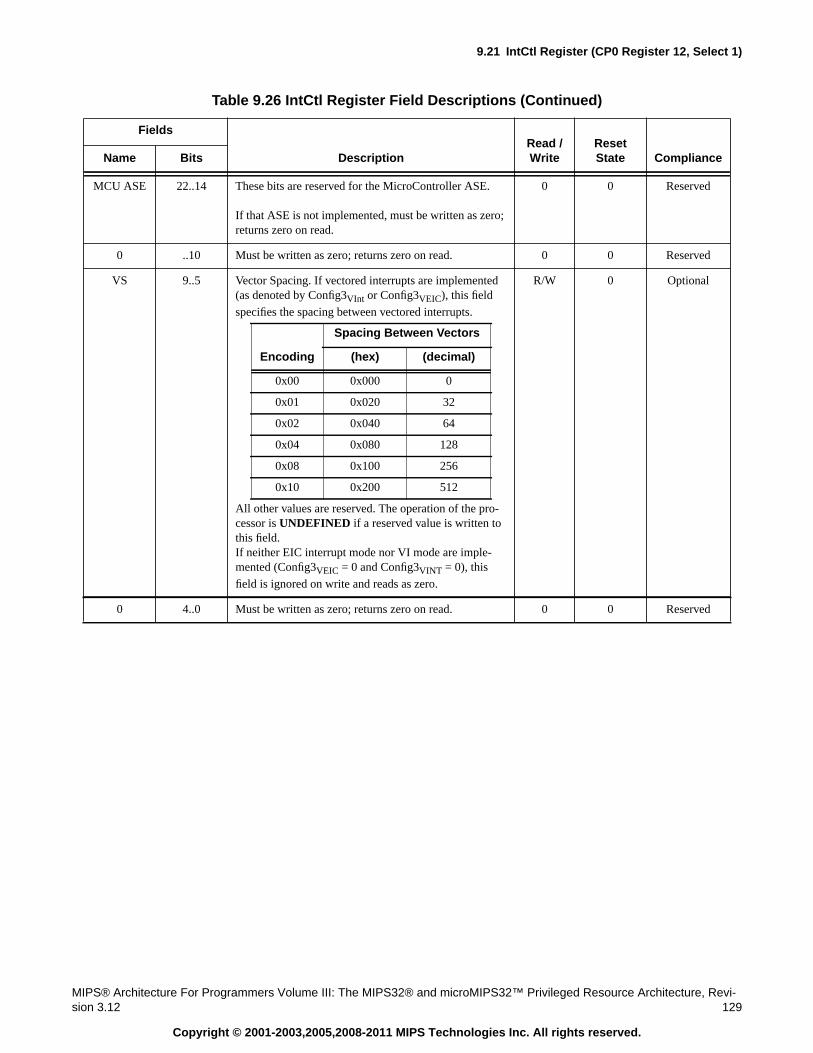
9.21 IntCtl Register (CP0 Register 12, Select 1)
MIPS® Architecture For Programmers Volume III: The MIPS32® and microMIPS32™ Privileged Resource Architecture, Revi-sion 3.12 129
Copyright © 2001-2003,2005,2008-2011 MIPS Technologies Inc. All rights reserved.
MCU ASE 22..14 These bits are reserved for the MicroController ASE.
If that ASE is not implemented, must be written as zero;returns zero on read.
0 0 Reserved
0 ..10 Must be written as zero; returns zero on read. 0 0 Reserved
VS 9..5 Vector Spacing. If vectored interrupts are implemented(as denoted by Config3VInt or Config3VEIC), this field
specifies the spacing between vectored interrupts.
All other values are reserved. The operation of the pro-cessor is UNDEFINED if a reserved value is written tothis field.If neither EIC interrupt mode nor VI mode are imple-mented (Config3VEIC = 0 and Config3VINT = 0), this
field is ignored on write and reads as zero.
R/W 0 Optional
0 4..0 Must be written as zero; returns zero on read. 0 0 Reserved
Table 9.26 IntCtl Register Field Descriptions (Continued)
Fields
DescriptionRead /Write
ResetState ComplianceName Bits
Encoding
Spacing Between Vectors
(hex) (decimal)
0x00 0x000 0
0x01 0x020 32
0x02 0x040 64
0x04 0x080 128
0x08 0x100 256
0x10 0x200 512
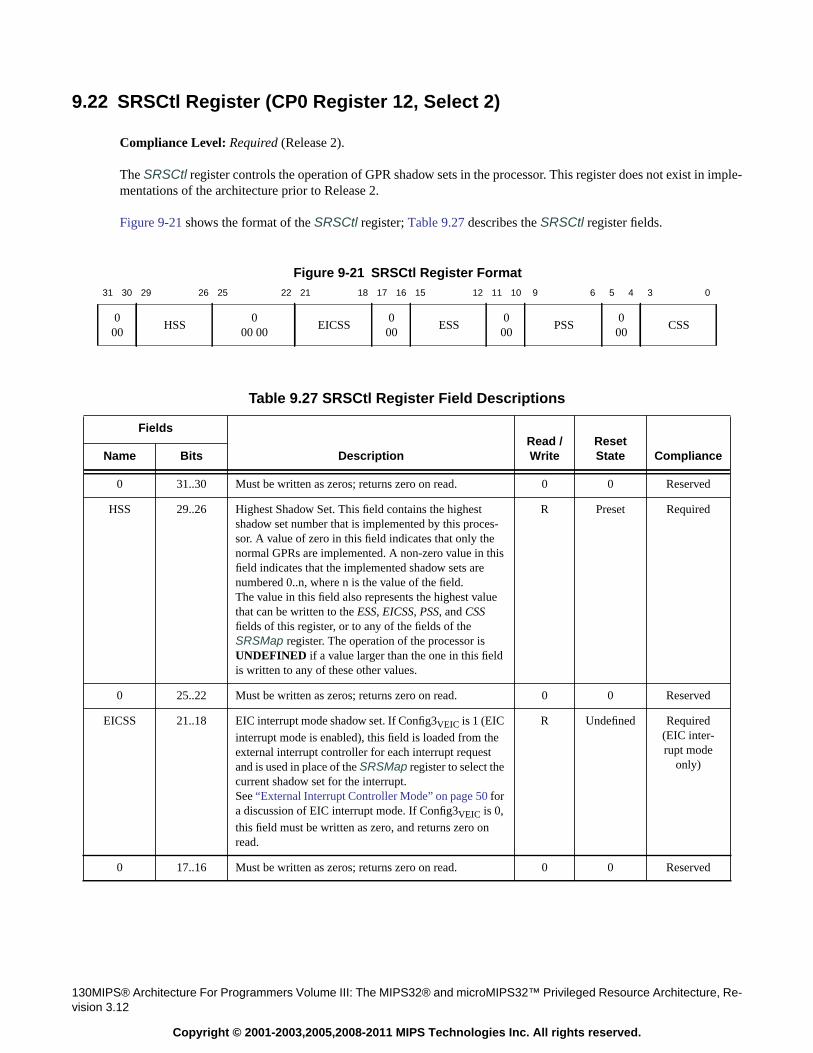
130MIPS® Architecture For Programmers Volume III: The MIPS32® and microMIPS32™ Privileged Resource Architecture, Re-vision 3.12
Copyright © 2001-2003,2005,2008-2011 MIPS Technologies Inc. All rights reserved.
9.22 SRSCtl Register (CP0 Register 12, Select 2)
Compliance Level: Required (Release 2).
The SRSCtl register controls the operation of GPR shadow sets in the processor. This register does not exist in imple-mentations of the architecture prior to Release 2.
Figure 9-21 shows the format of the SRSCtl register; Table 9.27 describes the SRSCtl register fields.
Figure 9-21 SRSCtl Register Format31 30 29 26 25 22 21 18 17 16 15 12 11 10 9 6 5 4 3 0
000
HSS0
00 00EICSS
000
ESS000
PSS000
CSS
Table 9.27 SRSCtl Register Field Descriptions
Fields
DescriptionRead /Write
ResetState ComplianceName Bits
0 31..30 Must be written as zeros; returns zero on read. 0 0 Reserved
HSS 29..26 Highest Shadow Set. This field contains the highestshadow set number that is implemented by this proces-sor. A value of zero in this field indicates that only thenormal GPRs are implemented. A non-zero value in thisfield indicates that the implemented shadow sets arenumbered 0..n, where n is the value of the field.The value in this field also represents the highest valuethat can be written to the ESS, EICSS, PSS, and CSSfields of this register, or to any of the fields of theSRSMap register. The operation of the processor isUNDEFINED if a value larger than the one in this fieldis written to any of these other values.
R Preset Required
0 25..22 Must be written as zeros; returns zero on read. 0 0 Reserved
EICSS 21..18 EIC interrupt mode shadow set. If Config3VEIC is 1 (EIC
interrupt mode is enabled), this field is loaded from theexternal interrupt controller for each interrupt requestand is used in place of the SRSMap register to select thecurrent shadow set for the interrupt.See “External Interrupt Controller Mode” on page 50 fora discussion of EIC interrupt mode. If Config3VEIC is 0,
this field must be written as zero, and returns zero onread.
R Undefined Required(EIC inter-rupt mode
only)
0 17..16 Must be written as zeros; returns zero on read. 0 0 Reserved
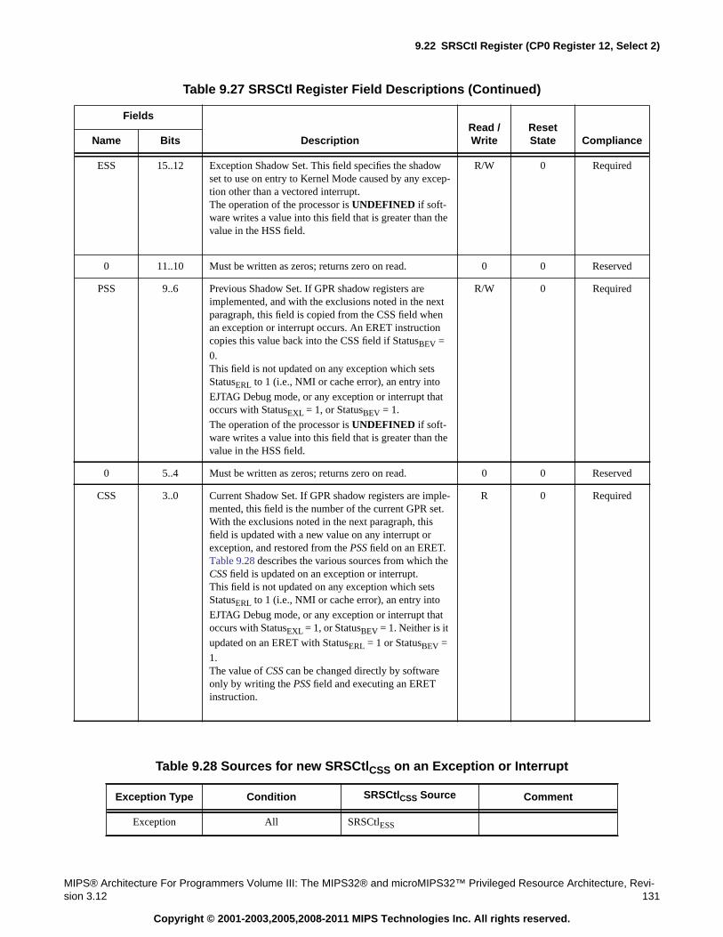
9.22 SRSCtl Register (CP0 Register 12, Select 2)
MIPS® Architecture For Programmers Volume III: The MIPS32® and microMIPS32™ Privileged Resource Architecture, Revi-sion 3.12 131
Copyright © 2001-2003,2005,2008-2011 MIPS Technologies Inc. All rights reserved.
ESS 15..12 Exception Shadow Set. This field specifies the shadowset to use on entry to Kernel Mode caused by any excep-tion other than a vectored interrupt.The operation of the processor is UNDEFINED if soft-ware writes a value into this field that is greater than thevalue in the HSS field.
R/W 0 Required
0 11..10 Must be written as zeros; returns zero on read. 0 0 Reserved
PSS 9..6 Previous Shadow Set. If GPR shadow registers areimplemented, and with the exclusions noted in the nextparagraph, this field is copied from the CSS field whenan exception or interrupt occurs. An ERET instructioncopies this value back into the CSS field if StatusBEV =
0.This field is not updated on any exception which setsStatusERL to 1 (i.e., NMI or cache error), an entry into
EJTAG Debug mode, or any exception or interrupt thatoccurs with StatusEXL = 1, or StatusBEV = 1.
The operation of the processor is UNDEFINED if soft-ware writes a value into this field that is greater than thevalue in the HSS field.
R/W 0 Required
0 5..4 Must be written as zeros; returns zero on read. 0 0 Reserved
CSS 3..0 Current Shadow Set. If GPR shadow registers are imple-mented, this field is the number of the current GPR set.With the exclusions noted in the next paragraph, thisfield is updated with a new value on any interrupt orexception, and restored from the PSS field on an ERET.Table 9.28 describes the various sources from which theCSS field is updated on an exception or interrupt.This field is not updated on any exception which setsStatusERL to 1 (i.e., NMI or cache error), an entry into
EJTAG Debug mode, or any exception or interrupt thatoccurs with StatusEXL = 1, or StatusBEV = 1. Neither is it
updated on an ERET with StatusERL = 1 or StatusBEV =
1.The value of CSS can be changed directly by softwareonly by writing the PSS field and executing an ERETinstruction.
R 0 Required
Table 9.28 Sources for new SRSCtlCSS on an Exception or Interrupt
Exception Type Condition SRSCtlCSS Source Comment
Exception All SRSCtlESS
Table 9.27 SRSCtl Register Field Descriptions (Continued)
Fields
DescriptionRead /Write
ResetState ComplianceName Bits
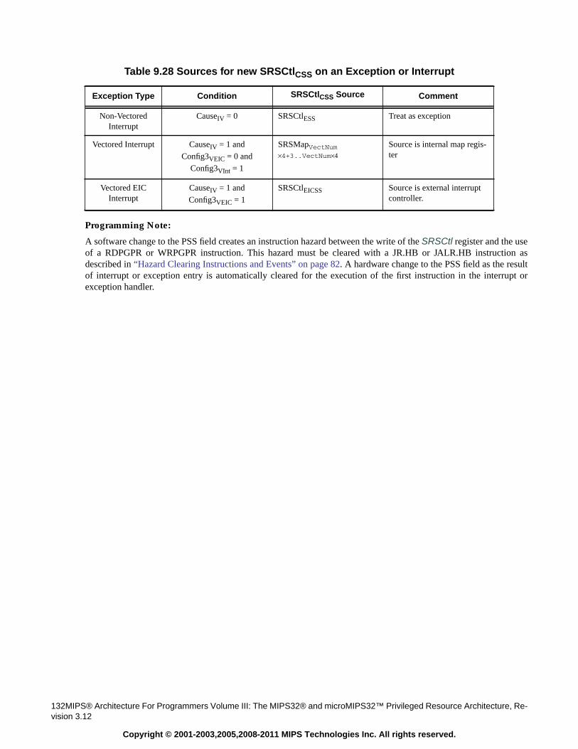
132MIPS® Architecture For Programmers Volume III: The MIPS32® and microMIPS32™ Privileged Resource Architecture, Re-vision 3.12
Copyright © 2001-2003,2005,2008-2011 MIPS Technologies Inc. All rights reserved.
Programming Note:
A software change to the PSS field creates an instruction hazard between the write of the SRSCtl register and the useof a RDPGPR or WRPGPR instruction. This hazard must be cleared with a JR.HB or JALR.HB instruction asdescribed in “Hazard Clearing Instructions and Events” on page 82. A hardware change to the PSS field as the resultof interrupt or exception entry is automatically cleared for the execution of the first instruction in the interrupt orexception handler.
Non-VectoredInterrupt
CauseIV = 0 SRSCtlESS Treat as exception
Vectored Interrupt CauseIV = 1 and
Config3VEIC = 0 and
Config3VInt = 1
SRSMapVectNum×4+3..VectNum×4
Source is internal map regis-ter
Vectored EICInterrupt
CauseIV = 1 and
Config3VEIC = 1
SRSCtlEICSS Source is external interruptcontroller.
Table 9.28 Sources for new SRSCtlCSS on an Exception or Interrupt
Exception Type Condition SRSCtlCSS Source Comment
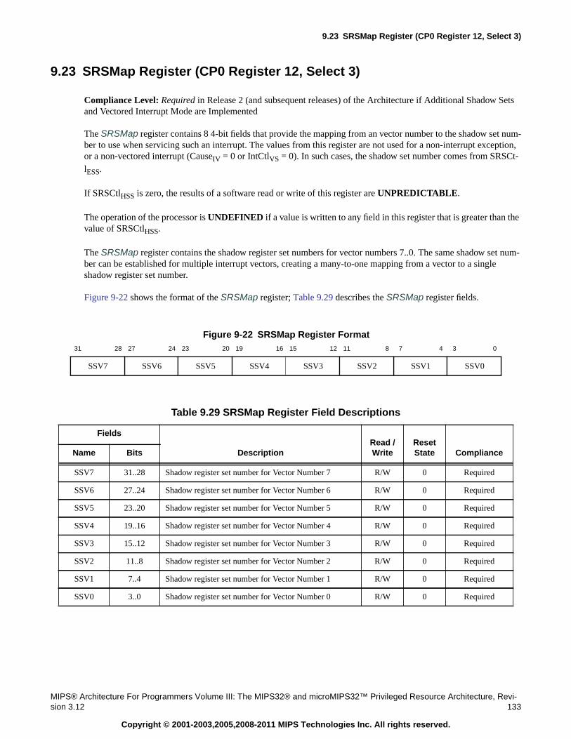
9.23 SRSMap Register (CP0 Register 12, Select 3)
MIPS® Architecture For Programmers Volume III: The MIPS32® and microMIPS32™ Privileged Resource Architecture, Revi-sion 3.12 133
Copyright © 2001-2003,2005,2008-2011 MIPS Technologies Inc. All rights reserved.
9.23 SRSMap Register (CP0 Register 12, Select 3)
Compliance Level: Required in Release 2 (and subsequent releases) of the Architecture if Additional Shadow Setsand Vectored Interrupt Mode are Implemented
The SRSMap register contains 8 4-bit fields that provide the mapping from an vector number to the shadow set num-ber to use when servicing such an interrupt. The values from this register are not used for a non-interrupt exception,or a non-vectored interrupt (CauseIV = 0 or IntCtlVS = 0). In such cases, the shadow set number comes from SRSCt-lESS.
If SRSCtlHSS is zero, the results of a software read or write of this register are UNPREDICTABLE.
The operation of the processor is UNDEFINED if a value is written to any field in this register that is greater than thevalue of SRSCtlHSS.
The SRSMap register contains the shadow register set numbers for vector numbers 7..0. The same shadow set num-ber can be established for multiple interrupt vectors, creating a many-to-one mapping from a vector to a singleshadow register set number.
Figure 9-22 shows the format of the SRSMap register; Table 9.29 describes the SRSMap register fields.
Figure 9-22 SRSMap Register Format31 28 27 24 23 20 19 16 15 12 11 8 7 4 3 0
SSV7 SSV6 SSV5 SSV4 SSV3 SSV2 SSV1 SSV0
Table 9.29 SRSMap Register Field Descriptions
Fields
DescriptionRead /Write
ResetState ComplianceName Bits
SSV7 31..28 Shadow register set number for Vector Number 7 R/W 0 Required
SSV6 27..24 Shadow register set number for Vector Number 6 R/W 0 Required
SSV5 23..20 Shadow register set number for Vector Number 5 R/W 0 Required
SSV4 19..16 Shadow register set number for Vector Number 4 R/W 0 Required
SSV3 15..12 Shadow register set number for Vector Number 3 R/W 0 Required
SSV2 11..8 Shadow register set number for Vector Number 2 R/W 0 Required
SSV1 7..4 Shadow register set number for Vector Number 1 R/W 0 Required
SSV0 3..0 Shadow register set number for Vector Number 0 R/W 0 Required
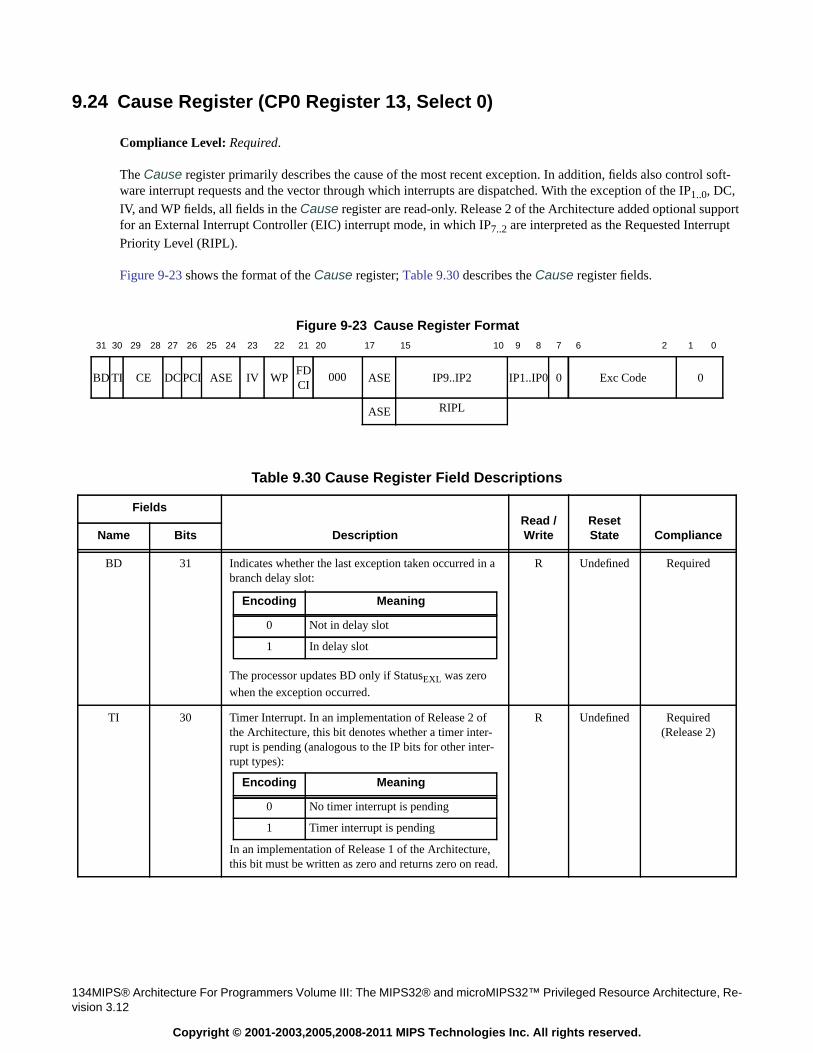
134MIPS® Architecture For Programmers Volume III: The MIPS32® and microMIPS32™ Privileged Resource Architecture, Re-vision 3.12
Copyright © 2001-2003,2005,2008-2011 MIPS Technologies Inc. All rights reserved.
9.24 Cause Register (CP0 Register 13, Select 0)
Compliance Level: Required.
The Cause register primarily describes the cause of the most recent exception. In addition, fields also control soft-ware interrupt requests and the vector through which interrupts are dispatched. With the exception of the IP1..0, DC,IV, and WP fields, all fields in the Cause register are read-only. Release 2 of the Architecture added optional supportfor an External Interrupt Controller (EIC) interrupt mode, in which IP7..2 are interpreted as the Requested InterruptPriority Level (RIPL).
Figure 9-23 shows the format of the Cause register; Table 9.30 describes the Cause register fields.
Figure 9-23 Cause Register Format31 30 29 28 27 26 25 24 23 22 21 20 17 15 10 9 8 7 6 2 1 0
BD TI CE DC PCI ASE IV WPFDCI
000 ASE IP9..IP2 IP1..IP0 0 Exc Code 0
ASE RIPL
Table 9.30 Cause Register Field Descriptions
Fields
DescriptionRead /Write
ResetState ComplianceName Bits
BD 31 Indicates whether the last exception taken occurred in abranch delay slot:
The processor updates BD only if StatusEXL was zero
when the exception occurred.
R Undefined Required
TI 30 Timer Interrupt. In an implementation of Release 2 ofthe Architecture, this bit denotes whether a timer inter-rupt is pending (analogous to the IP bits for other inter-rupt types):
In an implementation of Release 1 of the Architecture,this bit must be written as zero and returns zero on read.
R Undefined Required(Release 2)
Encoding Meaning
0 Not in delay slot
1 In delay slot
Encoding Meaning
0 No timer interrupt is pending
1 Timer interrupt is pending
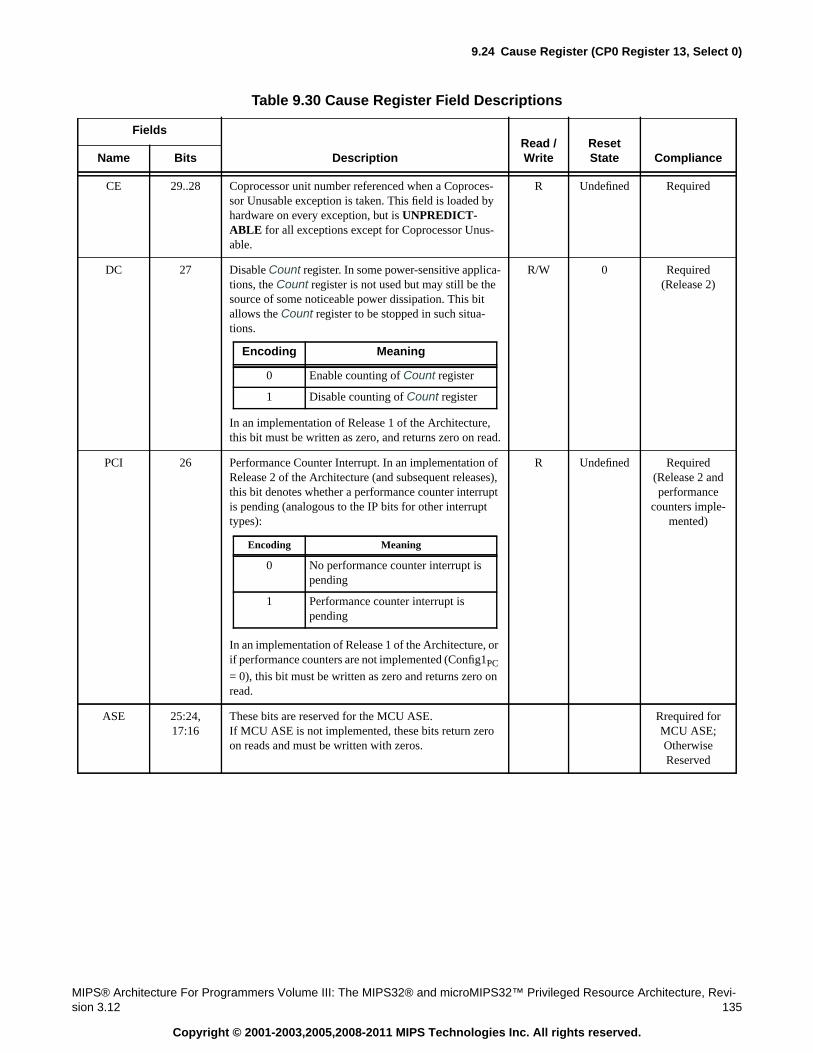
9.24 Cause Register (CP0 Register 13, Select 0)
MIPS® Architecture For Programmers Volume III: The MIPS32® and microMIPS32™ Privileged Resource Architecture, Revi-sion 3.12 135
Copyright © 2001-2003,2005,2008-2011 MIPS Technologies Inc. All rights reserved.
CE 29..28 Coprocessor unit number referenced when a Coproces-sor Unusable exception is taken. This field is loaded byhardware on every exception, but is UNPREDICT-ABLE for all exceptions except for Coprocessor Unus-able.
R Undefined Required
DC 27 Disable Count register. In some power-sensitive applica-tions, the Count register is not used but may still be thesource of some noticeable power dissipation. This bitallows the Count register to be stopped in such situa-tions.
In an implementation of Release 1 of the Architecture,this bit must be written as zero, and returns zero on read.
R/W 0 Required(Release 2)
PCI 26 Performance Counter Interrupt. In an implementation ofRelease 2 of the Architecture (and subsequent releases),this bit denotes whether a performance counter interruptis pending (analogous to the IP bits for other interrupttypes):
In an implementation of Release 1 of the Architecture, orif performance counters are not implemented (Config1PC
= 0), this bit must be written as zero and returns zero onread.
R Undefined Required(Release 2 andperformance
counters imple-mented)
ASE 25:24,17:16
These bits are reserved for the MCU ASE.If MCU ASE is not implemented, these bits return zeroon reads and must be written with zeros.
Rrequired forMCU ASE;OtherwiseReserved
Table 9.30 Cause Register Field Descriptions
Fields
DescriptionRead /Write
ResetState ComplianceName Bits
Encoding Meaning
0 Enable counting of Count register
1 Disable counting of Count register
Encoding Meaning
0 No performance counter interrupt ispending
1 Performance counter interrupt ispending
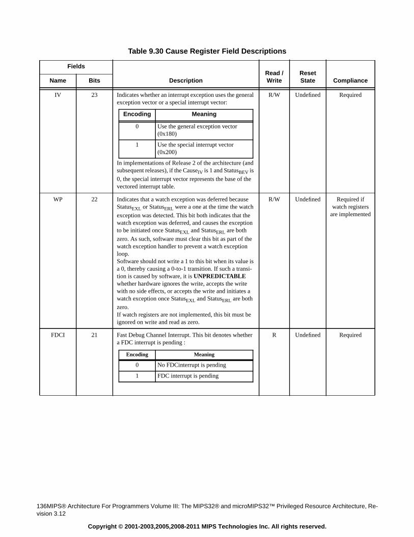
136MIPS® Architecture For Programmers Volume III: The MIPS32® and microMIPS32™ Privileged Resource Architecture, Re-vision 3.12
Copyright © 2001-2003,2005,2008-2011 MIPS Technologies Inc. All rights reserved.
IV 23 Indicates whether an interrupt exception uses the generalexception vector or a special interrupt vector:
In implementations of Release 2 of the architecture (andsubsequent releases), if the CauseIV is 1 and StatusBEV is
0, the special interrupt vector represents the base of thevectored interrupt table.
R/W Undefined Required
WP 22 Indicates that a watch exception was deferred becauseStatusEXL or StatusERL were a one at the time the watch
exception was detected. This bit both indicates that thewatch exception was deferred, and causes the exceptionto be initiated once StatusEXL and StatusERL are both
zero. As such, software must clear this bit as part of thewatch exception handler to prevent a watch exceptionloop.Software should not write a 1 to this bit when its value isa 0, thereby causing a 0-to-1 transition. If such a transi-tion is caused by software, it is UNPREDICTABLEwhether hardware ignores the write, accepts the writewith no side effects, or accepts the write and initiates awatch exception once StatusEXL and StatusERL are both
zero.If watch registers are not implemented, this bit must beignored on write and read as zero.
R/W Undefined Required ifwatch registers
are implemented
FDCI 21 Fast Debug Channel Interrupt. This bit denotes whethera FDC interrupt is pending :
R Undefined Required
Table 9.30 Cause Register Field Descriptions
Fields
DescriptionRead /Write
ResetState ComplianceName Bits
Encoding Meaning
0 Use the general exception vector(0x180)
1 Use the special interrupt vector(0x200)
Encoding Meaning
0 No FDCinterrupt is pending
1 FDC interrupt is pending
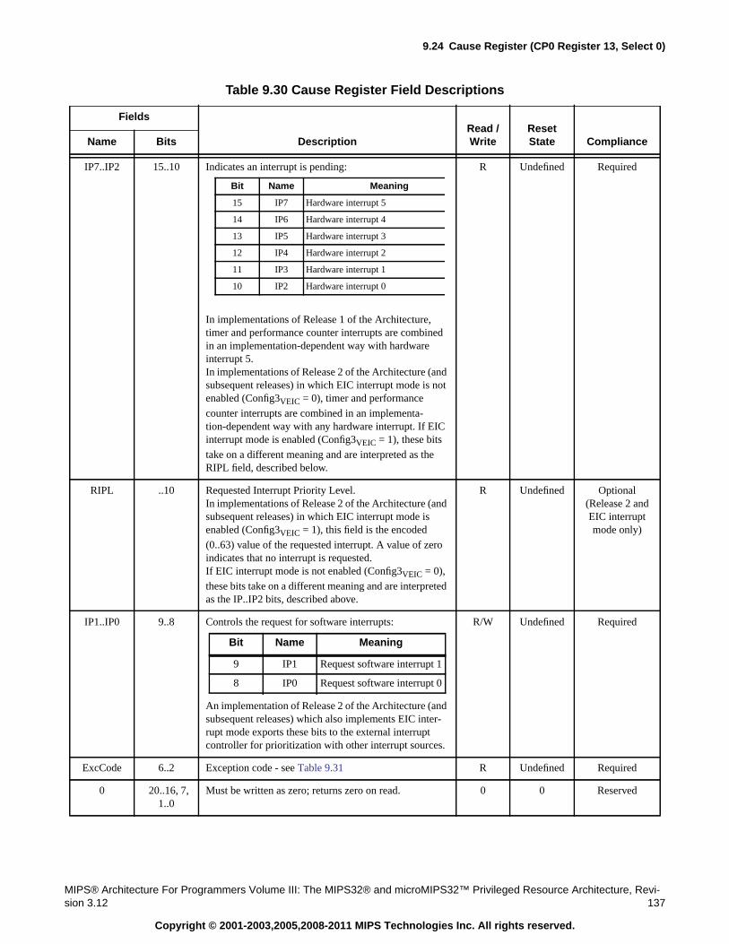
9.24 Cause Register (CP0 Register 13, Select 0)
MIPS® Architecture For Programmers Volume III: The MIPS32® and microMIPS32™ Privileged Resource Architecture, Revi-sion 3.12 137
Copyright © 2001-2003,2005,2008-2011 MIPS Technologies Inc. All rights reserved.
IP7..IP2 15..10 Indicates an interrupt is pending:
In implementations of Release 1 of the Architecture,timer and performance counter interrupts are combinedin an implementation-dependent way with hardwareinterrupt 5.In implementations of Release 2 of the Architecture (andsubsequent releases) in which EIC interrupt mode is notenabled (Config3VEIC = 0), timer and performance
counter interrupts are combined in an implementa-tion-dependent way with any hardware interrupt. If EICinterrupt mode is enabled (Config3VEIC = 1), these bits
take on a different meaning and are interpreted as theRIPL field, described below.
R Undefined Required
RIPL ..10 Requested Interrupt Priority Level.In implementations of Release 2 of the Architecture (andsubsequent releases) in which EIC interrupt mode isenabled (Config3VEIC = 1), this field is the encoded
(0..63) value of the requested interrupt. A value of zeroindicates that no interrupt is requested.If EIC interrupt mode is not enabled (Config3VEIC = 0),
these bits take on a different meaning and are interpretedas the IP..IP2 bits, described above.
R Undefined Optional(Release 2 andEIC interruptmode only)
IP1..IP0 9..8 Controls the request for software interrupts:
An implementation of Release 2 of the Architecture (andsubsequent releases) which also implements EIC inter-rupt mode exports these bits to the external interruptcontroller for prioritization with other interrupt sources.
R/W Undefined Required
ExcCode 6..2 Exception code - see Table 9.31 R Undefined Required
0 20..16, 7,1..0
Must be written as zero; returns zero on read. 0 0 Reserved
Table 9.30 Cause Register Field Descriptions
Fields
DescriptionRead /Write
ResetState ComplianceName Bits
Bit Name Meaning
15 IP7 Hardware interrupt 5
14 IP6 Hardware interrupt 4
13 IP5 Hardware interrupt 3
12 IP4 Hardware interrupt 2
11 IP3 Hardware interrupt 1
10 IP2 Hardware interrupt 0
Bit Name Meaning
9 IP1 Request software interrupt 1
8 IP0 Request software interrupt 0
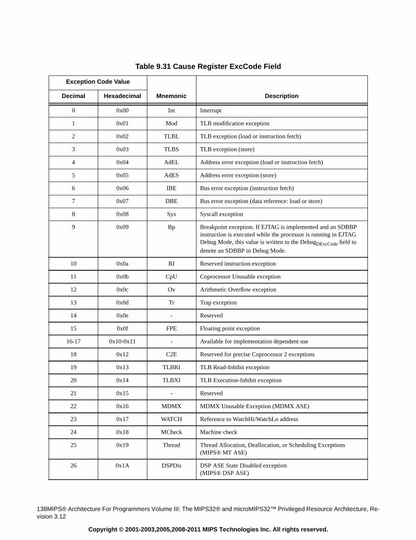
138MIPS® Architecture For Programmers Volume III: The MIPS32® and microMIPS32™ Privileged Resource Architecture, Re-vision 3.12
Copyright © 2001-2003,2005,2008-2011 MIPS Technologies Inc. All rights reserved.
Table 9.31 Cause Register ExcCode Field
Exception Code Value
Mnemonic DescriptionDecimal Hexadecimal
0 0x00 Int Interrupt
1 0x01 Mod TLB modification exception
2 0x02 TLBL TLB exception (load or instruction fetch)
3 0x03 TLBS TLB exception (store)
4 0x04 AdEL Address error exception (load or instruction fetch)
5 0x05 AdES Address error exception (store)
6 0x06 IBE Bus error exception (instruction fetch)
7 0x07 DBE Bus error exception (data reference: load or store)
8 0x08 Sys Syscall exception
9 0x09 Bp Breakpoint exception. If EJTAG is implemented and an SDBBPinstruction is executed while the processor is running in EJTAGDebug Mode, this value is written to the DebugDExcCode field to
denote an SDBBP in Debug Mode.
10 0x0a RI Reserved instruction exception
11 0x0b CpU Coprocessor Unusable exception
12 0x0c Ov Arithmetic Overflow exception
13 0x0d Tr Trap exception
14 0x0e - Reserved
15 0x0f FPE Floating point exception
16-17 0x10-0x11 - Available for implementation dependent use
18 0x12 C2E Reserved for precise Coprocessor 2 exceptions
19 0x13 TLBRI TLB Read-Inhibit exception
20 0x14 TLBXI TLB Execution-Inhibit exception
21 0x15 - Reserved
22 0x16 MDMX MDMX Unusable Exception (MDMX ASE)
23 0x17 WATCH Reference to WatchHi/WatchLo address
24 0x18 MCheck Machine check
25 0x19 Thread Thread Allocation, Deallocation, or Scheduling Exceptions(MIPS® MT ASE)
26 0x1A DSPDis DSP ASE State Disabled exception(MIPS® DSP ASE)
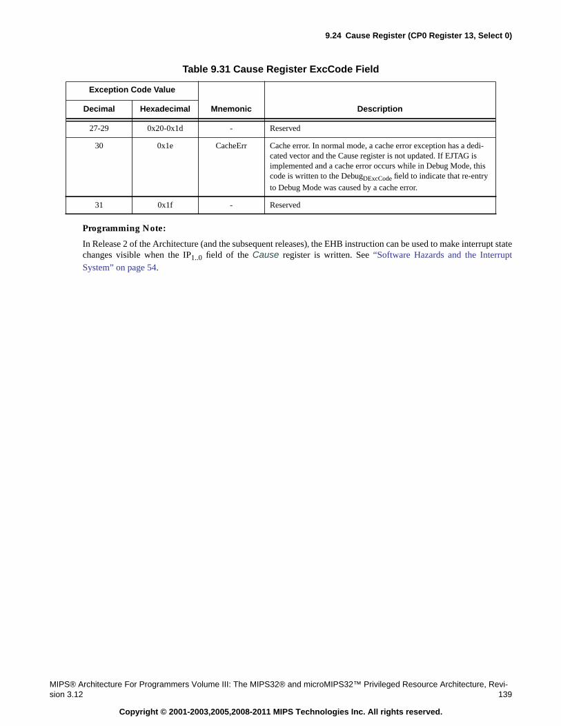
9.24 Cause Register (CP0 Register 13, Select 0)
MIPS® Architecture For Programmers Volume III: The MIPS32® and microMIPS32™ Privileged Resource Architecture, Revi-sion 3.12 139
Copyright © 2001-2003,2005,2008-2011 MIPS Technologies Inc. All rights reserved.
Programming Note:
In Release 2 of the Architecture (and the subsequent releases), the EHB instruction can be used to make interrupt statechanges visible when the IP1..0 field of the Cause register is written. See “Software Hazards and the InterruptSystem” on page 54.
27-29 0x20-0x1d - Reserved
30 0x1e CacheErr Cache error. In normal mode, a cache error exception has a dedi-cated vector and the Cause register is not updated. If EJTAG isimplemented and a cache error occurs while in Debug Mode, thiscode is written to the DebugDExcCode field to indicate that re-entry
to Debug Mode was caused by a cache error.
31 0x1f - Reserved
Table 9.31 Cause Register ExcCode Field
Exception Code Value
Mnemonic DescriptionDecimal Hexadecimal
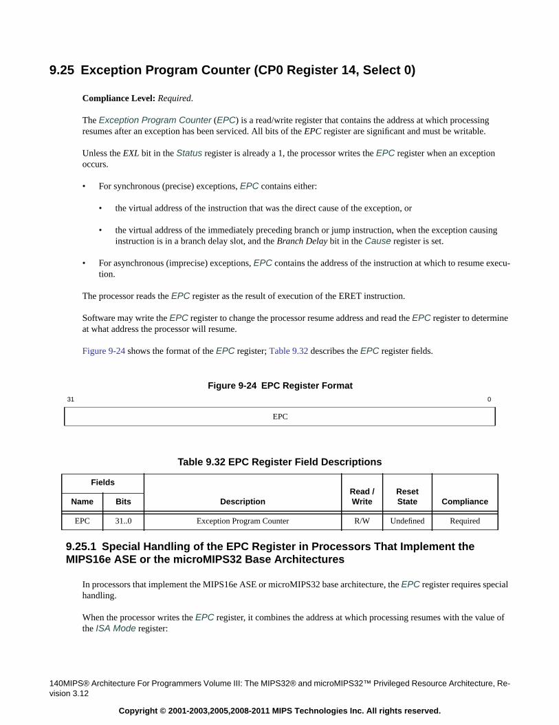
140MIPS® Architecture For Programmers Volume III: The MIPS32® and microMIPS32™ Privileged Resource Architecture, Re-vision 3.12
Copyright © 2001-2003,2005,2008-2011 MIPS Technologies Inc. All rights reserved.
9.25 Exception Program Counter (CP0 Register 14, Select 0)
Compliance Level: Required.
The Exception Program Counter (EPC) is a read/write register that contains the address at which processingresumes after an exception has been serviced. All bits of the EPC register are significant and must be writable.
Unless the EXL bit in the Status register is already a 1, the processor writes the EPC register when an exceptionoccurs.
• For synchronous (precise) exceptions, EPC contains either:
• the virtual address of the instruction that was the direct cause of the exception, or
• the virtual address of the immediately preceding branch or jump instruction, when the exception causinginstruction is in a branch delay slot, and the Branch Delay bit in the Cause register is set.
• For asynchronous (imprecise) exceptions, EPC contains the address of the instruction at which to resume execu-tion.
The processor reads the EPC register as the result of execution of the ERET instruction.
Software may write the EPC register to change the processor resume address and read the EPC register to determineat what address the processor will resume.
Figure 9-24 shows the format of the EPC register; Table 9.32 describes the EPC register fields.
9.25.1 Special Handling of the EPC Register in Processors That Implement theMIPS16e ASE or the microMIPS32 Base Architectures
In processors that implement the MIPS16e ASE or microMIPS32 base architecture, the EPC register requires specialhandling.
When the processor writes the EPC register, it combines the address at which processing resumes with the value ofthe ISA Mode register:
Figure 9-24 EPC Register Format31 0
EPC
Table 9.32 EPC Register Field Descriptions
Fields
DescriptionRead /Write
ResetState ComplianceName Bits
EPC 31..0 Exception Program Counter R/W Undefined Required
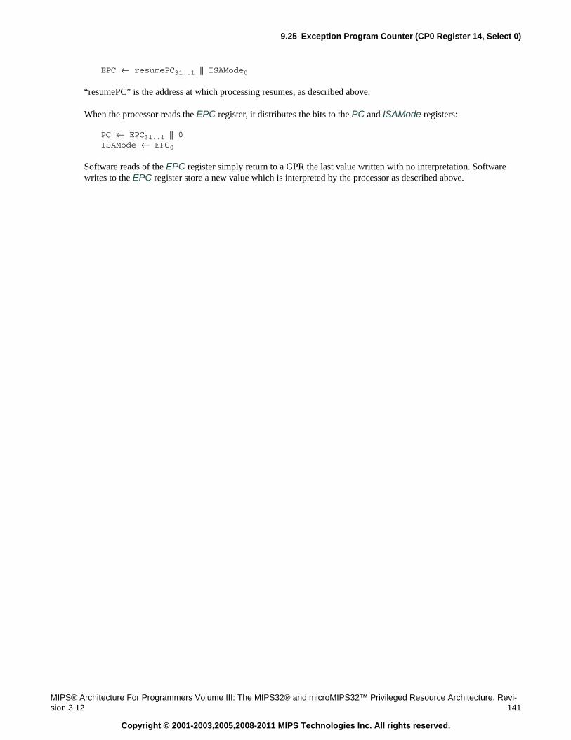
9.25 Exception Program Counter (CP0 Register 14, Select 0)
MIPS® Architecture For Programmers Volume III: The MIPS32® and microMIPS32™ Privileged Resource Architecture, Revi-sion 3.12 141
Copyright © 2001-2003,2005,2008-2011 MIPS Technologies Inc. All rights reserved.
EPC ← resumePC31..1 || ISAMode0
“resumePC” is the address at which processing resumes, as described above.
When the processor reads the EPC register, it distributes the bits to the PC and ISAMode registers:
PC ← EPC31..1 || 0ISAMode ← EPC0
Software reads of the EPC register simply return to a GPR the last value written with no interpretation. Softwarewrites to the EPC register store a new value which is interpreted by the processor as described above.
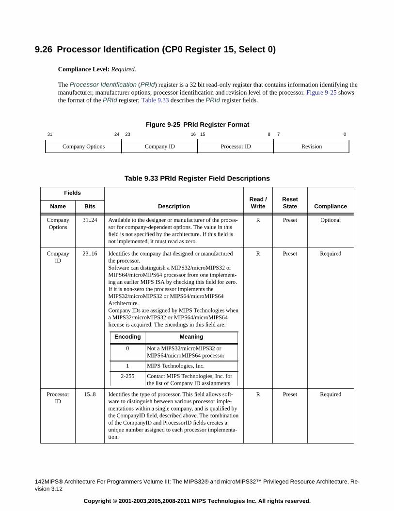
142MIPS® Architecture For Programmers Volume III: The MIPS32® and microMIPS32™ Privileged Resource Architecture, Re-vision 3.12
Copyright © 2001-2003,2005,2008-2011 MIPS Technologies Inc. All rights reserved.
9.26 Processor Identification (CP0 Register 15, Select 0)
Compliance Level: Required.
The Processor Identification (PRId) register is a 32 bit read-only register that contains information identifying themanufacturer, manufacturer options, processor identification and revision level of the processor. Figure 9-25 showsthe format of the PRId register; Table 9.33 describes the PRId register fields.
Figure 9-25 PRId Register Format31 24 23 16 15 8 7 0
Company Options Company ID Processor ID Revision
Table 9.33 PRId Register Field Descriptions
Fields
DescriptionRead /Write
ResetState ComplianceName Bits
CompanyOptions
31..24 Available to the designer or manufacturer of the proces-sor for company-dependent options. The value in thisfield is not specified by the architecture. If this field isnot implemented, it must read as zero.
R Preset Optional
CompanyID
23..16 Identifies the company that designed or manufacturedthe processor.Software can distinguish a MIPS32/microMIPS32 orMIPS64/microMIPS64 processor from one implement-ing an earlier MIPS ISA by checking this field for zero.If it is non-zero the processor implements theMIPS32/microMIPS32 or MIPS64/microMIPS64Architecture.Company IDs are assigned by MIPS Technologies whena MIPS32/microMIPS32 or MIPS64/microMIPS64license is acquired. The encodings in this field are:
R Preset Required
ProcessorID
15..8 Identifies the type of processor. This field allows soft-ware to distinguish between various processor imple-mentations within a single company, and is qualified bythe CompanyID field, described above. The combinationof the CompanyID and ProcessorID fields creates aunique number assigned to each processor implementa-tion.
R Preset Required
Encoding Meaning
0 Not a MIPS32/microMIPS32 orMIPS64/microMIPS64 processor
1 MIPS Technologies, Inc.
2-255 Contact MIPS Technologies, Inc. forthe list of Company ID assignments
9.26 Processor Identification (CP0 Register 15, Select 0)
MIPS® Architecture For Programmers Volume III: The MIPS32® and microMIPS32™ Privileged Resource Architecture, Revi-sion 3.12 143
Copyright © 2001-2003,2005,2008-2011 MIPS Technologies Inc. All rights reserved.
Software should not use the fields of this register to infer configuration information about the processor. Rather, theconfiguration registers should be used to determine the capabilities of the processor. Programmers who identify casesin which the configuration registers are not sufficient, requiring them to revert to check on the PRId register value,should send email to [email protected], reporting the specific case.
Revision 7..0 Specifies the revision number of the processor. This fieldallows software to distinguish between one revision andanother of the same processor type. If this field is notimplemented, it must read as zero.
R Preset Optional
Table 9.33 PRId Register Field Descriptions
Fields
DescriptionRead /Write
ResetState ComplianceName Bits
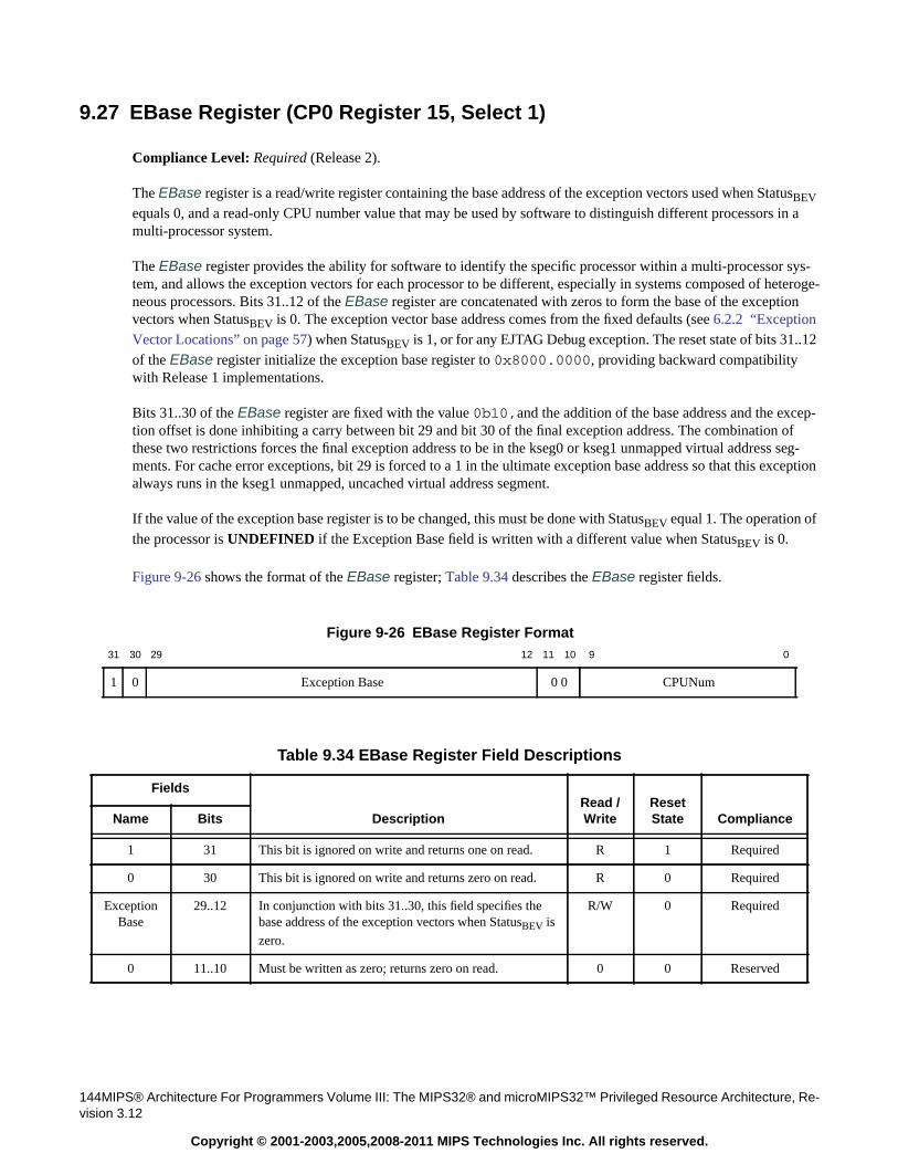
144MIPS® Architecture For Programmers Volume III: The MIPS32® and microMIPS32™ Privileged Resource Architecture, Re-vision 3.12
Copyright © 2001-2003,2005,2008-2011 MIPS Technologies Inc. All rights reserved.
9.27 EBase Register (CP0 Register 15, Select 1)
Compliance Level: Required (Release 2).
The EBase register is a read/write register containing the base address of the exception vectors used when StatusBEV
equals 0, and a read-only CPU number value that may be used by software to distinguish different processors in amulti-processor system.
The EBase register provides the ability for software to identify the specific processor within a multi-processor sys-tem, and allows the exception vectors for each processor to be different, especially in systems composed of heteroge-neous processors. Bits 31..12 of the EBase register are concatenated with zeros to form the base of the exceptionvectors when StatusBEV is 0. The exception vector base address comes from the fixed defaults (see 6.2.2 “ExceptionVector Locations” on page 57) when StatusBEV is 1, or for any EJTAG Debug exception. The reset state of bits 31..12of the EBase register initialize the exception base register to 0x8000.0000, providing backward compatibilitywith Release 1 implementations.
Bits 31..30 of the EBase register are fixed with the value 0b10,and the addition of the base address and the excep-tion offset is done inhibiting a carry between bit 29 and bit 30 of the final exception address. The combination ofthese two restrictions forces the final exception address to be in the kseg0 or kseg1 unmapped virtual address seg-ments. For cache error exceptions, bit 29 is forced to a 1 in the ultimate exception base address so that this exceptionalways runs in the kseg1 unmapped, uncached virtual address segment.
If the value of the exception base register is to be changed, this must be done with StatusBEV equal 1. The operation ofthe processor is UNDEFINED if the Exception Base field is written with a different value when StatusBEV is 0.
Figure 9-26 shows the format of the EBase register; Table 9.34 describes the EBase register fields.
Figure 9-26 EBase Register Format31 30 29 12 11 10 9 0
1 0 Exception Base 0 0 CPUNum
Table 9.34 EBase Register Field Descriptions
Fields
DescriptionRead /Write
ResetState ComplianceName Bits
1 31 This bit is ignored on write and returns one on read. R 1 Required
0 30 This bit is ignored on write and returns zero on read. R 0 Required
ExceptionBase
29..12 In conjunction with bits 31..30, this field specifies thebase address of the exception vectors when StatusBEV is
zero.
R/W 0 Required
0 11..10 Must be written as zero; returns zero on read. 0 0 Reserved
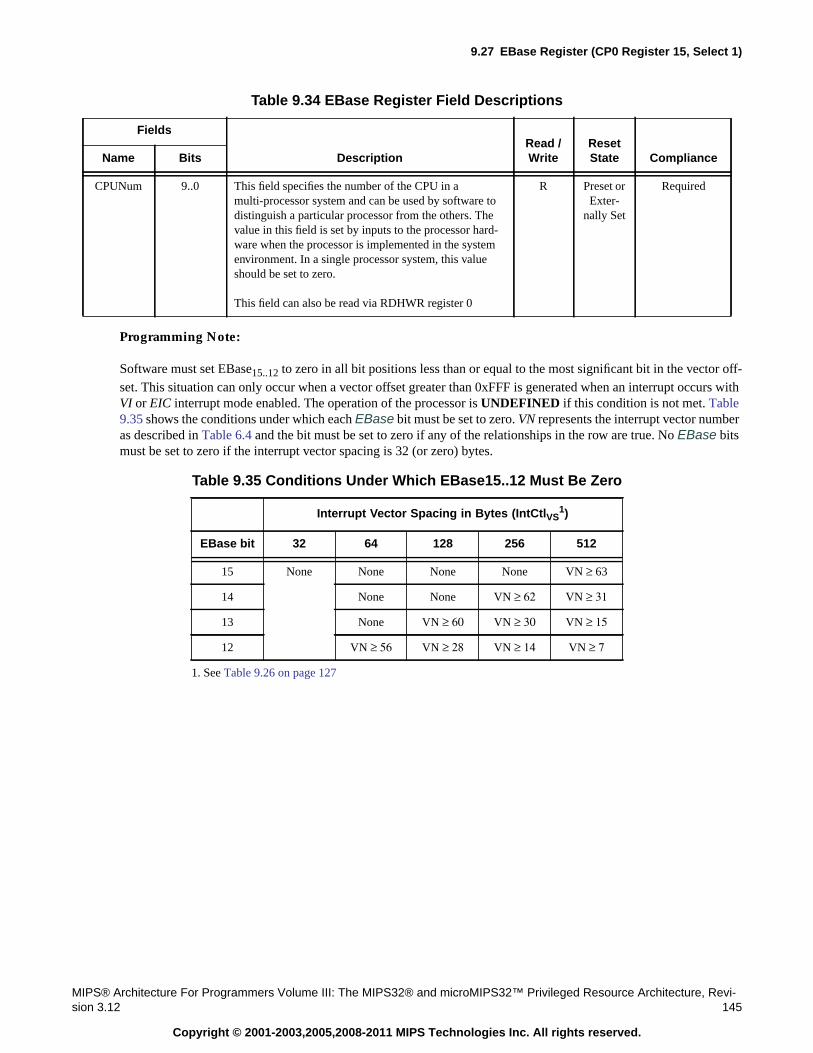
9.27 EBase Register (CP0 Register 15, Select 1)
MIPS® Architecture For Programmers Volume III: The MIPS32® and microMIPS32™ Privileged Resource Architecture, Revi-sion 3.12 145
Copyright © 2001-2003,2005,2008-2011 MIPS Technologies Inc. All rights reserved.
Programming Note:
Software must set EBase15..12 to zero in all bit positions less than or equal to the most significant bit in the vector off-set. This situation can only occur when a vector offset greater than 0xFFF is generated when an interrupt occurs withVI or EIC interrupt mode enabled. The operation of the processor is UNDEFINED if this condition is not met. Table9.35 shows the conditions under which each EBase bit must be set to zero. VN represents the interrupt vector numberas described in Table 6.4 and the bit must be set to zero if any of the relationships in the row are true. No EBase bitsmust be set to zero if the interrupt vector spacing is 32 (or zero) bytes.
CPUNum 9..0 This field specifies the number of the CPU in amulti-processor system and can be used by software todistinguish a particular processor from the others. Thevalue in this field is set by inputs to the processor hard-ware when the processor is implemented in the systemenvironment. In a single processor system, this valueshould be set to zero.
This field can also be read via RDHWR register 0
R Preset orExter-
nally Set
Required
Table 9.35 Conditions Under Which EBase15..12 Must Be Zero
Interrupt Vector Spacing in Bytes (IntCtlVS1)
1. See Table 9.26 on page 127
EBase bit 32 64 128 256 512
15 None None None None VN ≥ 63
14 None None VN ≥ 62 VN ≥ 31
13 None VN ≥ 60 VN ≥ 30 VN ≥ 15
12 VN ≥ 56 VN ≥ 28 VN ≥ 14 VN ≥ 7
Table 9.34 EBase Register Field Descriptions
Fields
DescriptionRead /Write
ResetState ComplianceName Bits
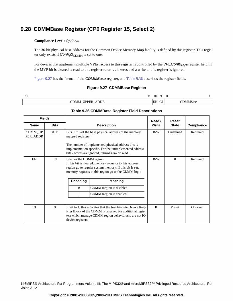
146MIPS® Architecture For Programmers Volume III: The MIPS32® and microMIPS32™ Privileged Resource Architecture, Re-vision 3.12
Copyright © 2001-2003,2005,2008-2011 MIPS Technologies Inc. All rights reserved.
9.28 CDMMBase Register (CP0 Register 15, Select 2)
Compliance Level: Optional.
The 36-bit physical base address for the Common Device Memory Map facility is defined by this register. This regis-ter only exists if Config3CDMM is set to one.
For devices that implement multiple VPEs, access to this register is controlled by the VPEConf0MVP register field. Ifthe MVP bit is cleared, a read to this register returns all zeros and a write to this register is ignored.
Figure 9.27 has the format of the CDMMBase register, and Table 9.36 describes the register fields.
Figure 9.27 CDMMBase Register
31 11 10 9 8 0
CDMM_UPPER_ADDR EN CI CDMMSize
Table 9.36 CDMMBase Register Field Descriptions
Fields
DescriptionRead /Write
ResetState ComplianceName Bits
CDMM_UPPER_ADDR
31:11 Bits 35:15 of the base physical address of the memorymapped registers.
The number of implemented physical address bits isimplementation specific. For the unimplemented addressbits - writes are ignored, returns zero on read.
R/W Undefined Required
EN 10 Enables the CDMM region.If this bit is cleared, memory requests to this addressregion go to regular system memory. If this bit is set,memory requests to this region go to the CDMM logic
R/W 0 Required
CI 9 If set to 1, this indicates that the first 64-byte Device Reg-ister Block of the CDMM is reserved for additional regis-ters which manage CDMM region behavior and are not IOdevice registers.
R Preset Optional
Encoding Meaning
0 CDMM Region is disabled.
1 CDMM Region is enabled.
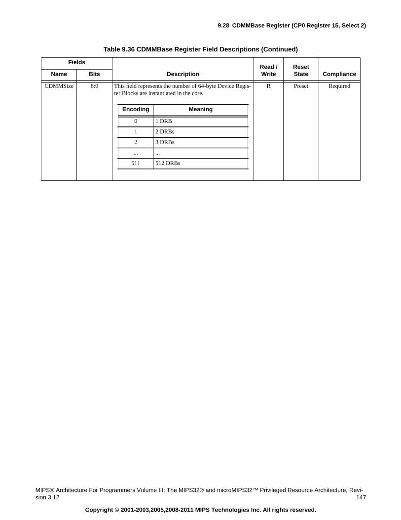
9.28 CDMMBase Register (CP0 Register 15, Select 2)
MIPS® Architecture For Programmers Volume III: The MIPS32® and microMIPS32™ Privileged Resource Architecture, Revi-sion 3.12 147
Copyright © 2001-2003,2005,2008-2011 MIPS Technologies Inc. All rights reserved.
CDMMSize 8:0 This field represents the number of 64-byte Device Regis-ter Blocks are instantiated in the core.
R Preset Required
Table 9.36 CDMMBase Register Field Descriptions (Continued)
Fields
DescriptionRead /Write
ResetState ComplianceName Bits
Encoding Meaning
0 1 DRB
1 2 DRBs
2 3 DRBs
... ...
511 512 DRBs
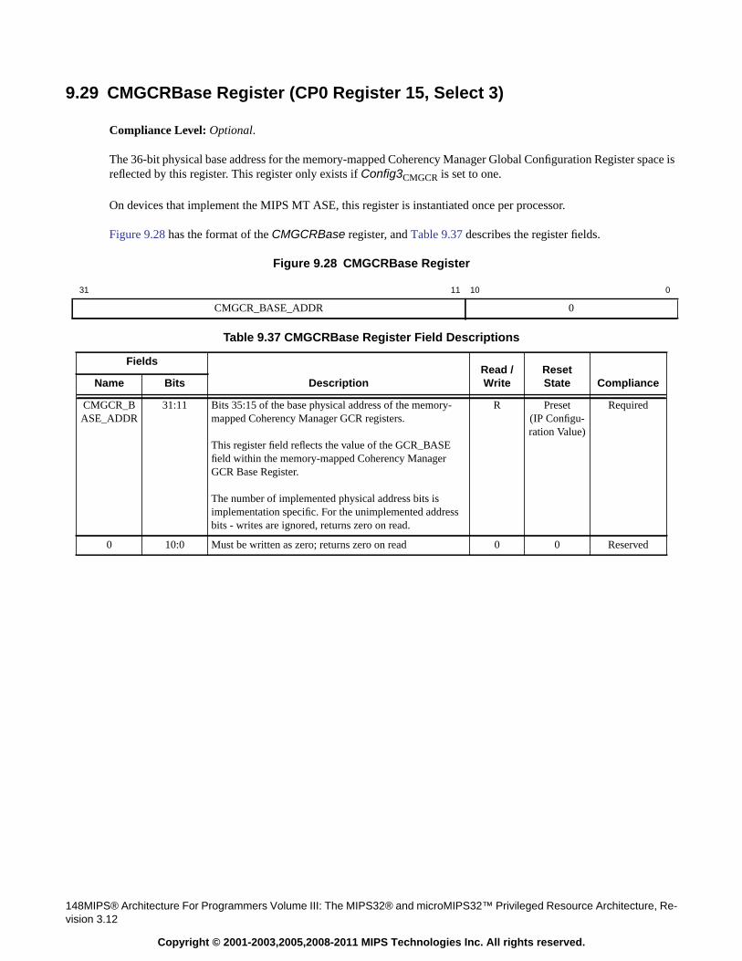
148MIPS® Architecture For Programmers Volume III: The MIPS32® and microMIPS32™ Privileged Resource Architecture, Re-vision 3.12
Copyright © 2001-2003,2005,2008-2011 MIPS Technologies Inc. All rights reserved.
9.29 CMGCRBase Register (CP0 Register 15, Select 3)
Compliance Level: Optional.
The 36-bit physical base address for the memory-mapped Coherency Manager Global Configuration Register space isreflected by this register. This register only exists if Config3CMGCR is set to one.
On devices that implement the MIPS MT ASE, this register is instantiated once per processor.
Figure 9.28 has the format of the CMGCRBase register, and Table 9.37 describes the register fields.
Figure 9.28 CMGCRBase Register
31 11 10 0
CMGCR_BASE_ADDR 0
Table 9.37 CMGCRBase Register Field Descriptions
Fields
DescriptionRead /Write
ResetState ComplianceName Bits
CMGCR_BASE_ADDR
31:11 Bits 35:15 of the base physical address of the memory-mapped Coherency Manager GCR registers.
This register field reflects the value of the GCR_BASEfield within the memory-mapped Coherency ManagerGCR Base Register.
The number of implemented physical address bits isimplementation specific. For the unimplemented addressbits - writes are ignored, returns zero on read.
R Preset(IP Configu-ration Value)
Required
0 10:0 Must be written as zero; returns zero on read 0 0 Reserved
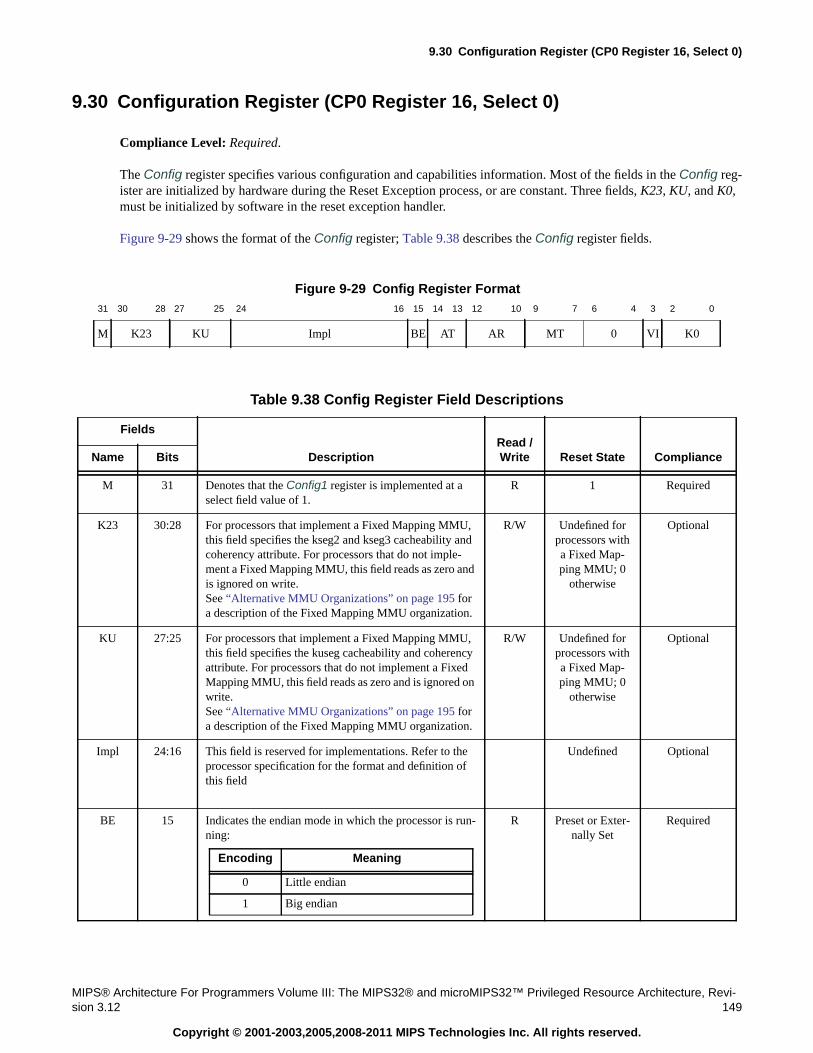
9.30 Configuration Register (CP0 Register 16, Select 0)
MIPS® Architecture For Programmers Volume III: The MIPS32® and microMIPS32™ Privileged Resource Architecture, Revi-sion 3.12 149
Copyright © 2001-2003,2005,2008-2011 MIPS Technologies Inc. All rights reserved.
9.30 Configuration Register (CP0 Register 16, Select 0)
Compliance Level: Required.
The Config register specifies various configuration and capabilities information. Most of the fields in the Config reg-ister are initialized by hardware during the Reset Exception process, or are constant. Three fields, K23, KU, and K0,must be initialized by software in the reset exception handler.
Figure 9-29 shows the format of the Config register; Table 9.38 describes the Config register fields.
Figure 9-29 Config Register Format31 30 28 27 25 24 16 15 14 13 12 10 9 7 6 4 3 2 0
M K23 KU Impl BE AT AR MT 0 VI K0
Table 9.38 Config Register Field Descriptions
Fields
DescriptionRead /Write Reset State ComplianceName Bits
M 31 Denotes that the Config1 register is implemented at aselect field value of 1.
R 1 Required
K23 30:28 For processors that implement a Fixed Mapping MMU,this field specifies the kseg2 and kseg3 cacheability andcoherency attribute. For processors that do not imple-ment a Fixed Mapping MMU, this field reads as zero andis ignored on write.See “Alternative MMU Organizations” on page 195 fora description of the Fixed Mapping MMU organization.
R/W Undefined forprocessors witha Fixed Map-ping MMU; 0
otherwise
Optional
KU 27:25 For processors that implement a Fixed Mapping MMU,this field specifies the kuseg cacheability and coherencyattribute. For processors that do not implement a FixedMapping MMU, this field reads as zero and is ignored onwrite.See “Alternative MMU Organizations” on page 195 fora description of the Fixed Mapping MMU organization.
R/W Undefined forprocessors witha Fixed Map-ping MMU; 0
otherwise
Optional
Impl 24:16 This field is reserved for implementations. Refer to theprocessor specification for the format and definition ofthis field
Undefined Optional
BE 15 Indicates the endian mode in which the processor is run-ning:
R Preset or Exter-nally Set
Required
Encoding Meaning
0 Little endian
1 Big endian
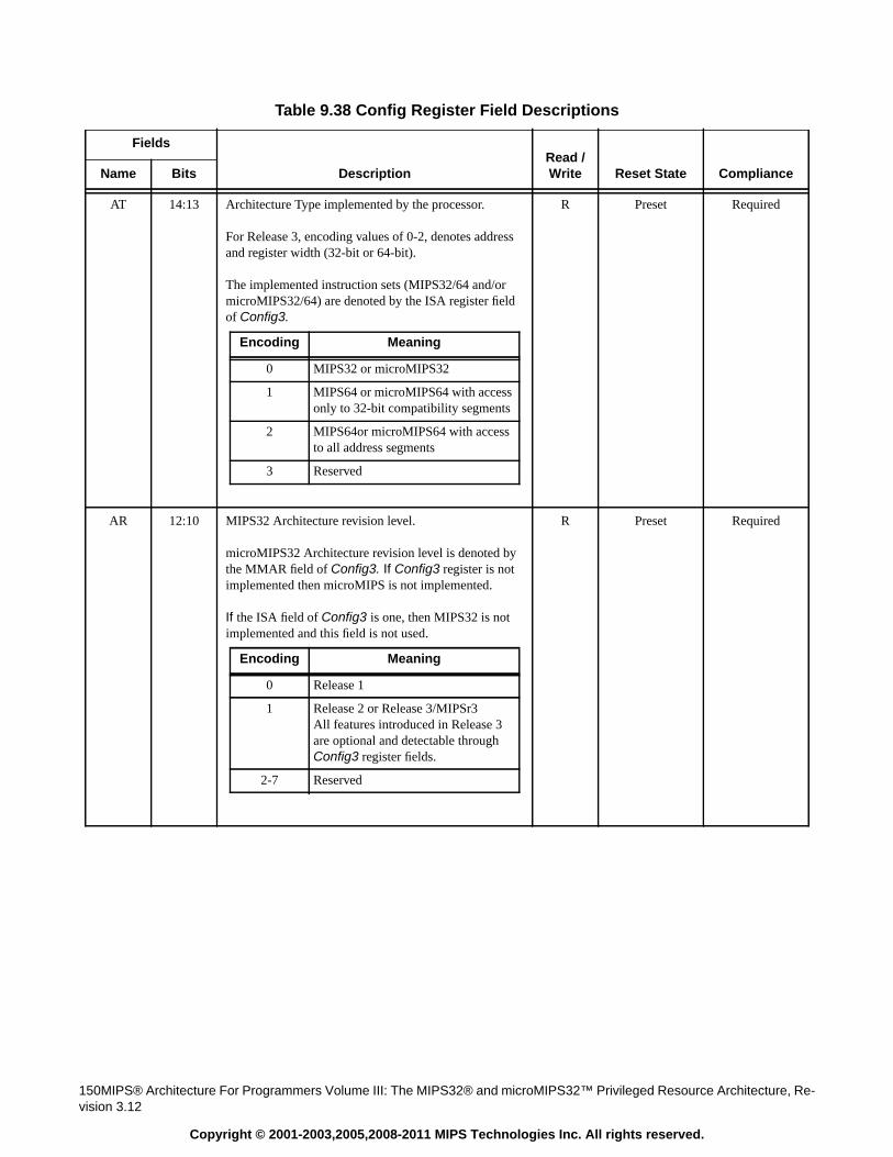
150MIPS® Architecture For Programmers Volume III: The MIPS32® and microMIPS32™ Privileged Resource Architecture, Re-vision 3.12
Copyright © 2001-2003,2005,2008-2011 MIPS Technologies Inc. All rights reserved.
AT 14:13 Architecture Type implemented by the processor.
For Release 3, encoding values of 0-2, denotes addressand register width (32-bit or 64-bit).
The implemented instruction sets (MIPS32/64 and/ormicroMIPS32/64) are denoted by the ISA register fieldof Config3.
R Preset Required
AR 12:10 MIPS32 Architecture revision level.
microMIPS32 Architecture revision level is denoted bythe MMAR field of Config3. If Config3 register is notimplemented then microMIPS is not implemented.
If the ISA field of Config3 is one, then MIPS32 is notimplemented and this field is not used.
R Preset Required
Table 9.38 Config Register Field Descriptions
Fields
DescriptionRead /Write Reset State ComplianceName Bits
Encoding Meaning
0 MIPS32 or microMIPS32
1 MIPS64 or microMIPS64 with accessonly to 32-bit compatibility segments
2 MIPS64or microMIPS64 with accessto all address segments
3 Reserved
Encoding Meaning
0 Release 1
1 Release 2 or Release 3/MIPSr3All features introduced in Release 3are optional and detectable throughConfig3 register fields.
2-7 Reserved
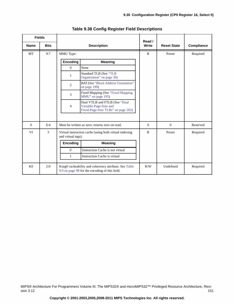
9.30 Configuration Register (CP0 Register 16, Select 0)
MIPS® Architecture For Programmers Volume III: The MIPS32® and microMIPS32™ Privileged Resource Architecture, Revi-sion 3.12 151
Copyright © 2001-2003,2005,2008-2011 MIPS Technologies Inc. All rights reserved.
MT 9:7 MMU Type: R Preset Required
0 6:4 Must be written as zero; returns zero on read. 0 0 Reserved
VI 3 Virtual instruction cache (using both virtual indexingand virtual tags):
R Preset Required
K0 2:0 Kseg0 cacheability and coherency attribute. See Table9.9 on page 98 for the encoding of this field.
R/W Undefined Required
Table 9.38 Config Register Field Descriptions
Fields
DescriptionRead /Write Reset State ComplianceName Bits
Encoding Meaning
0 None
1 Standard TLB (See “TLBOrganization” on page 30)
2 BAT (See “Block Address Translation”on page 199)
3 Fixed Mapping (See “Fixed MappingMMU” on page 195)
4Dual VTLB and FTLB (See “DualVariable-Page-Size andFixed-Page-Size TLBs” on page 202)
Encoding Meaning
0 Instruction Cache is not virtual
1 Instruction Cache is virtual
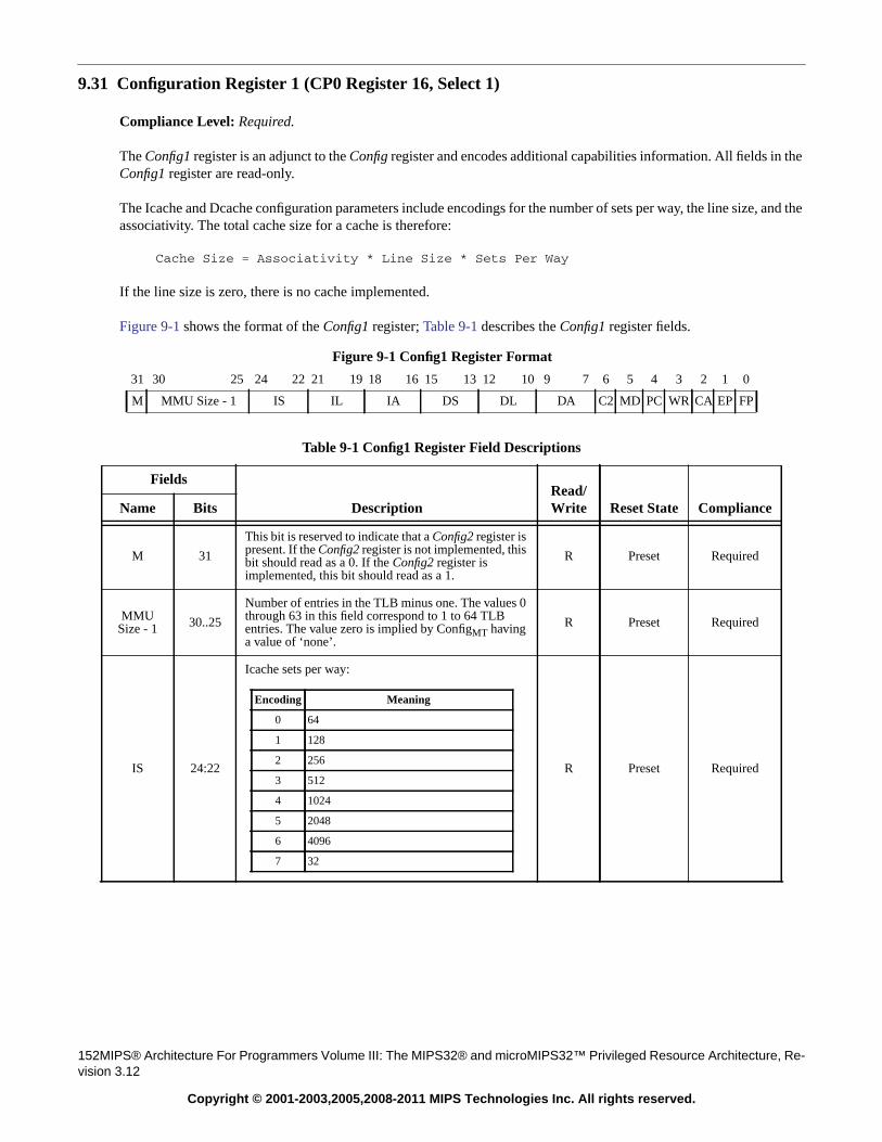
152MIPS® Architecture For Programmers Volume III: The MIPS32® and microMIPS32™ Privileged Resource Architecture, Re-vision 3.12
Copyright © 2001-2003,2005,2008-2011 MIPS Technologies Inc. All rights reserved.
9.31 Configuration Register 1 (CP0 Register 16, Select 1)
Compliance Level: Required.
The Config1 register is an adjunct to the Config register and encodes additional capabilities information. All fields in theConfig1 register are read-only.
The Icache and Dcache configuration parameters include encodings for the number of sets per way, the line size, and theassociativity. The total cache size for a cache is therefore:
Cache Size = Associativity * Line Size * Sets Per Way
If the line size is zero, there is no cache implemented.
Figure 9-1 shows the format of the Config1 register; Table 9-1 describes the Config1 register fields.
Figure 9-1 Config1 Register Format
31 30 25 24 22 21 19 18 16 15 13 12 10 9 7 6 5 4 3 2 1 0
M MMU Size - 1 IS IL IA DS DL DA C2 MD PC WR CA EP FP
Table 9-1 Config1 Register Field Descriptions
Fields
DescriptionRead/Write Reset State ComplianceName Bits
M 31
This bit is reserved to indicate that a Config2 register ispresent. If the Config2 register is not implemented, thisbit should read as a 0. If the Config2 register isimplemented, this bit should read as a 1.
R Preset Required
MMUSize - 1 30..25
Number of entries in the TLB minus one. The values 0through 63 in this field correspond to 1 to 64 TLBentries. The value zero is implied by ConfigMT havinga value of ‘none’.
R Preset Required
IS 24:22
Icache sets per way:
R Preset Required
Encoding Meaning
0 64
1 128
2 256
3 512
4 1024
5 2048
6 4096
7 32
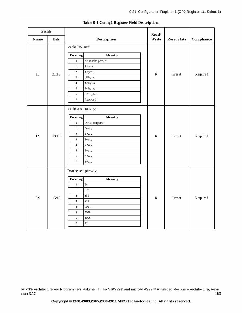
9.31 Configuration Register 1 (CP0 Register 16, Select 1)
MIPS® Architecture For Programmers Volume III: The MIPS32® and microMIPS32™ Privileged Resource Architecture, Revi-sion 3.12 153
Copyright © 2001-2003,2005,2008-2011 MIPS Technologies Inc. All rights reserved.
IL 21:19
Icache line size:
R Preset Required
IA 18:16
Icache associativity:
R Preset Required
DS 15:13
Dcache sets per way:
R Preset Required
Table 9-1 Config1 Register Field Descriptions
Fields
DescriptionRead/Write Reset State ComplianceName Bits
Encoding Meaning
0 No Icache present
1 4 bytes
2 8 bytes
3 16 bytes
4 32 bytes
5 64 bytes
6 128 bytes
7 Reserved
Encoding Meaning
0 Direct mapped
1 2-way
2 3-way
3 4-way
4 5-way
5 6-way
6 7-way
7 8-way
Encoding Meaning
0 64
1 128
2 256
3 512
4 1024
5 2048
6 4096
7 32
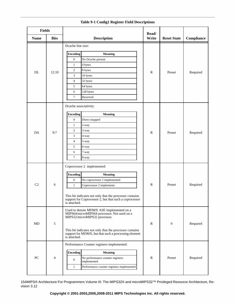
154MIPS® Architecture For Programmers Volume III: The MIPS32® and microMIPS32™ Privileged Resource Architecture, Re-vision 3.12
Copyright © 2001-2003,2005,2008-2011 MIPS Technologies Inc. All rights reserved.
DL 12:10
Dcache line size:
R Preset Required
DA 9:7
Dcache associativity:
R Preset Required
C2 6
Coprocessor 2 implemented:
This bit indicates not only that the processor containssupport for Coprocessor 2, but that such a coprocessoris attached.
R Preset Required
MD 5
Used to denote MDMX ASE implemented on aMIPS64/microMIPS64 processor. Not used on aMIPS32/microMIPS32 processor.
This bit indicates not only that the processor containssupport for MDMX, but that such a processing elementis attached.
R 0 Required
PC 4
Performance Counter registers implemented:
R Preset Required
Table 9-1 Config1 Register Field Descriptions
Fields
DescriptionRead/Write Reset State ComplianceName Bits
Encoding Meaning
0 No Dcache present
1 4 bytes
2 8 bytes
3 16 bytes
4 32 bytes
5 64 bytes
6 128 bytes
7 Reserved
Encoding Meaning
0 Direct mapped
1 2-way
2 3-way
3 4-way
4 5-way
5 6-way
6 7-way
7 8-way
Encoding Meaning
0 No coprocessor 2 implemented
1 Coprocessor 2 implements
Encoding Meaning
0No performance counter registersimplemented
1 Performance counter registers implemented
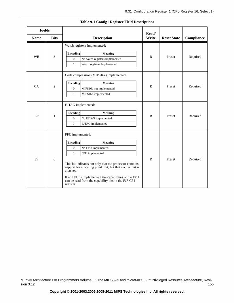
9.31 Configuration Register 1 (CP0 Register 16, Select 1)
MIPS® Architecture For Programmers Volume III: The MIPS32® and microMIPS32™ Privileged Resource Architecture, Revi-sion 3.12 155
Copyright © 2001-2003,2005,2008-2011 MIPS Technologies Inc. All rights reserved.
WR 3
Watch registers implemented:
R Preset Required
CA 2
Code compression (MIPS16e) implemented:
R Preset Required
EP 1
EJTAG implemented:
R Preset Required
FP 0
FPU implemented:
This bit indicates not only that the processor containssupport for a floating point unit, but that such a unit isattached.
If an FPU is implemented, the capabilities of the FPUcan be read from the capability bits in the FIR CP1register.
R Preset Required
Table 9-1 Config1 Register Field Descriptions
Fields
DescriptionRead/Write Reset State ComplianceName Bits
Encoding Meaning
0 No watch registers implemented
1 Watch registers implemented
Encoding Meaning
0 MIPS16e not implemented
1 MIPS16e implemented
Encoding Meaning
0 No EJTAG implemented
1 EJTAG implemented
Encoding Meaning
0 No FPU implemented
1 FPU implemented
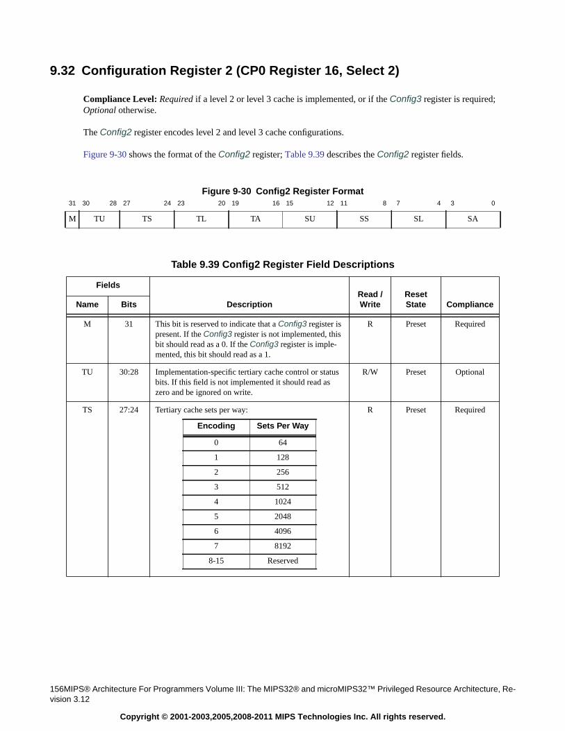
156MIPS® Architecture For Programmers Volume III: The MIPS32® and microMIPS32™ Privileged Resource Architecture, Re-vision 3.12
Copyright © 2001-2003,2005,2008-2011 MIPS Technologies Inc. All rights reserved.
9.32 Configuration Register 2 (CP0 Register 16, Select 2)
Compliance Level: Required if a level 2 or level 3 cache is implemented, or if the Config3 register is required;Optional otherwise.
The Config2 register encodes level 2 and level 3 cache configurations.
Figure 9-30 shows the format of the Config2 register; Table 9.39 describes the Config2 register fields.
Figure 9-30 Config2 Register Format31 30 28 27 24 23 20 19 16 15 12 11 8 7 4 3 0
M TU TS TL TA SU SS SL SA
Table 9.39 Config2 Register Field Descriptions
Fields
DescriptionRead /Write
ResetState ComplianceName Bits
M 31 This bit is reserved to indicate that a Config3 register ispresent. If the Config3 register is not implemented, thisbit should read as a 0. If the Config3 register is imple-mented, this bit should read as a 1.
R Preset Required
TU 30:28 Implementation-specific tertiary cache control or statusbits. If this field is not implemented it should read aszero and be ignored on write.
R/W Preset Optional
TS 27:24 Tertiary cache sets per way: R Preset Required
Encoding Sets Per Way
0 64
1 128
2 256
3 512
4 1024
5 2048
6 4096
7 8192
8-15 Reserved
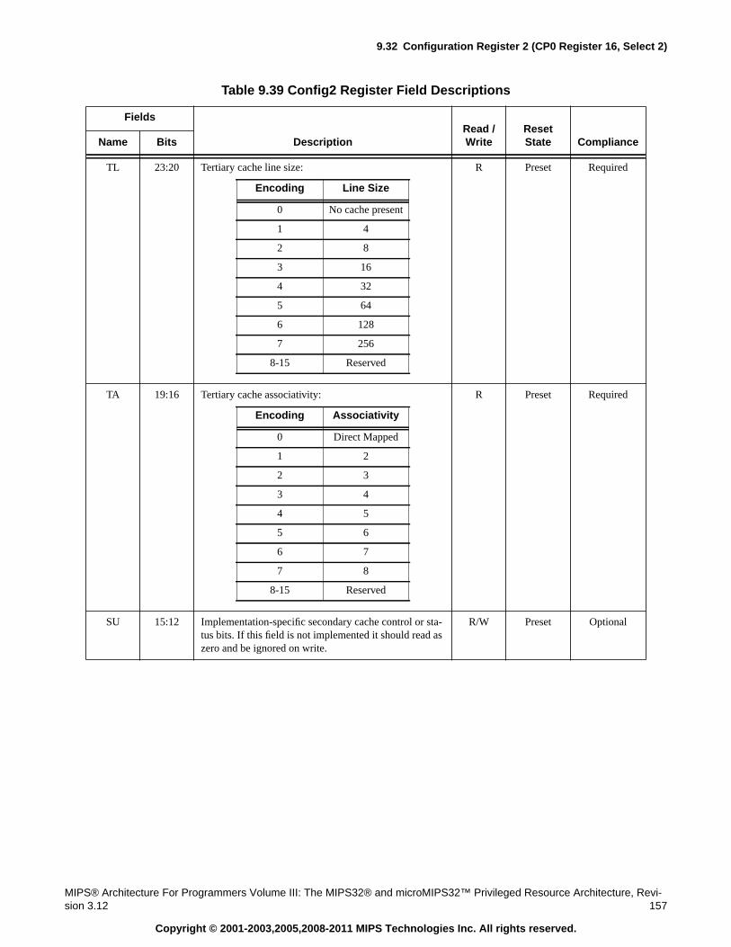
9.32 Configuration Register 2 (CP0 Register 16, Select 2)
MIPS® Architecture For Programmers Volume III: The MIPS32® and microMIPS32™ Privileged Resource Architecture, Revi-sion 3.12 157
Copyright © 2001-2003,2005,2008-2011 MIPS Technologies Inc. All rights reserved.
TL 23:20 Tertiary cache line size: R Preset Required
TA 19:16 Tertiary cache associativity: R Preset Required
SU 15:12 Implementation-specific secondary cache control or sta-tus bits. If this field is not implemented it should read aszero and be ignored on write.
R/W Preset Optional
Table 9.39 Config2 Register Field Descriptions
Fields
DescriptionRead /Write
ResetState ComplianceName Bits
Encoding Line Size
0 No cache present
1 4
2 8
3 16
4 32
5 64
6 128
7 256
8-15 Reserved
Encoding Associativity
0 Direct Mapped
1 2
2 3
3 4
4 5
5 6
6 7
7 8
8-15 Reserved
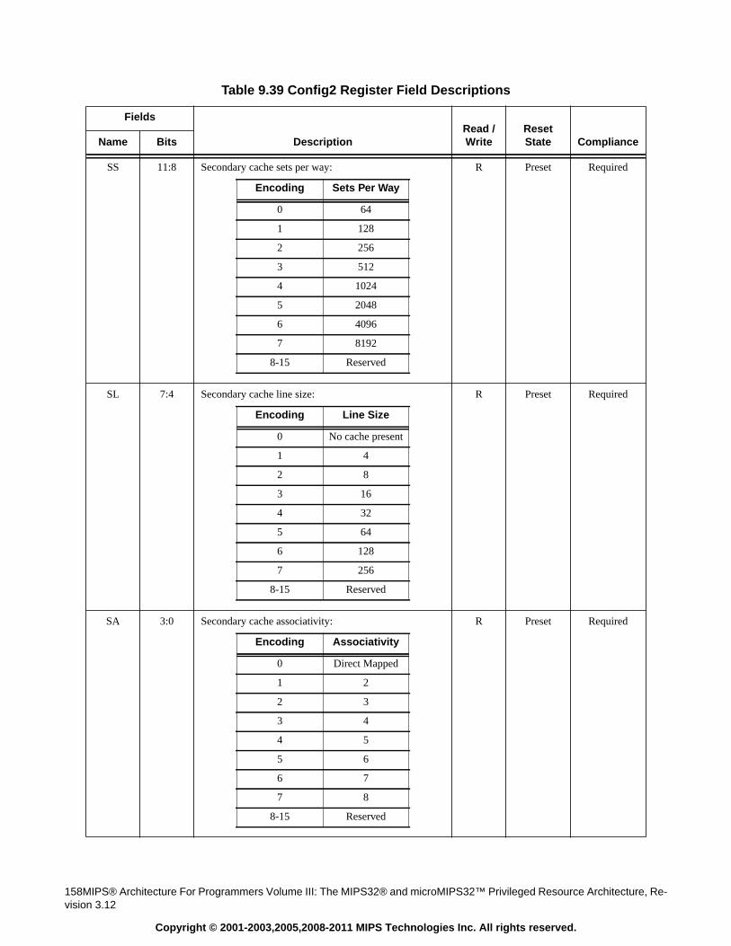
158MIPS® Architecture For Programmers Volume III: The MIPS32® and microMIPS32™ Privileged Resource Architecture, Re-vision 3.12
Copyright © 2001-2003,2005,2008-2011 MIPS Technologies Inc. All rights reserved.
SS 11:8 Secondary cache sets per way: R Preset Required
SL 7:4 Secondary cache line size: R Preset Required
SA 3:0 Secondary cache associativity: R Preset Required
Table 9.39 Config2 Register Field Descriptions
Fields
DescriptionRead /Write
ResetState ComplianceName Bits
Encoding Sets Per Way
0 64
1 128
2 256
3 512
4 1024
5 2048
6 4096
7 8192
8-15 Reserved
Encoding Line Size
0 No cache present
1 4
2 8
3 16
4 32
5 64
6 128
7 256
8-15 Reserved
Encoding Associativity
0 Direct Mapped
1 2
2 3
3 4
4 5
5 6
6 7
7 8
8-15 Reserved
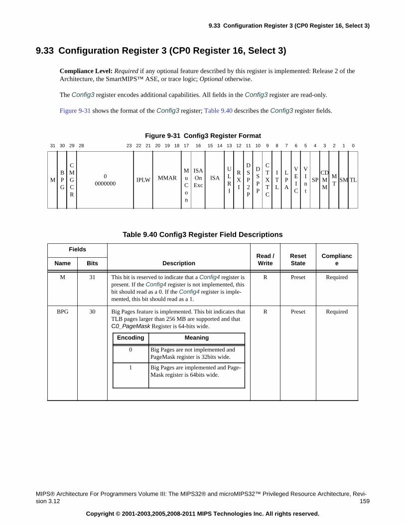
9.33 Configuration Register 3 (CP0 Register 16, Select 3)
MIPS® Architecture For Programmers Volume III: The MIPS32® and microMIPS32™ Privileged Resource Architecture, Revi-sion 3.12 159
Copyright © 2001-2003,2005,2008-2011 MIPS Technologies Inc. All rights reserved.
9.33 Configuration Register 3 (CP0 Register 16, Select 3)
Compliance Level: Required if any optional feature described by this register is implemented: Release 2 of theArchitecture, the SmartMIPS™ ASE, or trace logic; Optional otherwise.
The Config3 register encodes additional capabilities. All fields in the Config3 register are read-only.
Figure 9-31 shows the format of the Config3 register; Table 9.40 describes the Config3 register fields.
Figure 9-31 Config3 Register Format31 30 29 28 23 22 21 20 19 18 17 16 15 14 13 12 11 10 9 8 7 6 5 4 3 2 1 0
MBPG
CMGCR
00000000
IPLW MMARMuCon
ISAOnExc
ISA
ULRI
RXI
DSP2P
DSPP
CTXTC
ITL
LPA
VEIC
VInt
SPCDMM
MT
SM TL
Table 9.40 Config3 Register Field Descriptions
Fields
DescriptionRead /Write
ResetState
ComplianceName Bits
M 31 This bit is reserved to indicate that a Config4 register ispresent. If the Config4 register is not implemented, thisbit should read as a 0. If the Config4 register is imple-mented, this bit should read as a 1.
R Preset Required
BPG 30 Big Pages feature is implemented. This bit indicates thatTLB pages larger than 256 MB are supported and thatC0_PageMask Register is 64-bits wide.
R Preset Required
Encoding Meaning
0 Big Pages are not implemented andPageMask register is 32bits wide.
1 Big Pages are implemented and Page-Mask register is 64bits wide.
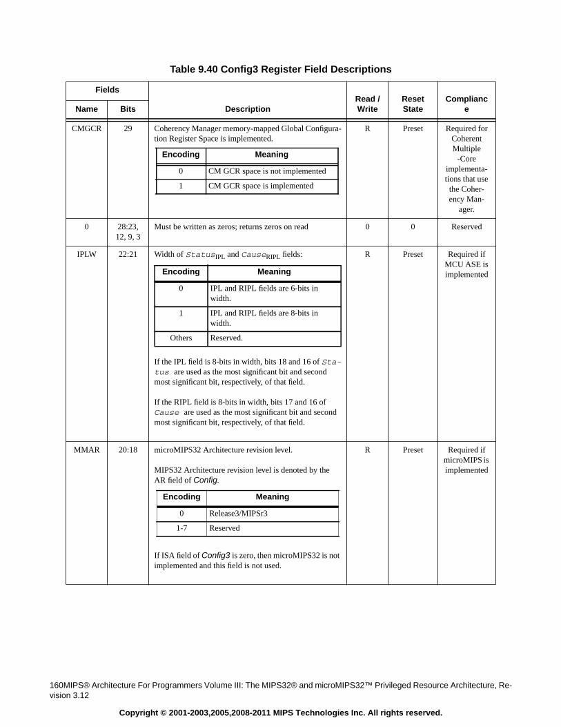
160MIPS® Architecture For Programmers Volume III: The MIPS32® and microMIPS32™ Privileged Resource Architecture, Re-vision 3.12
Copyright © 2001-2003,2005,2008-2011 MIPS Technologies Inc. All rights reserved.
CMGCR 29 Coherency Manager memory-mapped Global Configura-tion Register Space is implemented.
R Preset Required forCoherentMultiple
-Coreimplementa-tions that use
the Coher-ency Man-
ager.
0 28:23,12, 9, 3
Must be written as zeros; returns zeros on read 0 0 Reserved
IPLW 22:21 Width of StatusIPL and CauseRIPL fields:
If the IPL field is 8-bits in width, bits 18 and 16 of Sta-tus are used as the most significant bit and secondmost significant bit, respectively, of that field.
If the RIPL field is 8-bits in width, bits 17 and 16 ofCause are used as the most significant bit and secondmost significant bit, respectively, of that field.
R Preset Required ifMCU ASE isimplemented
MMAR 20:18 microMIPS32 Architecture revision level.
MIPS32 Architecture revision level is denoted by theAR field of Config.
If ISA field of Config3 is zero, then microMIPS32 is notimplemented and this field is not used.
R Preset Required ifmicroMIPS isimplemented
Table 9.40 Config3 Register Field Descriptions
Fields
DescriptionRead /Write
ResetState
ComplianceName Bits
Encoding Meaning
0 CM GCR space is not implemented
1 CM GCR space is implemented
Encoding Meaning
0 IPL and RIPL fields are 6-bits inwidth.
1 IPL and RIPL fields are 8-bits inwidth.
Others Reserved.
Encoding Meaning
0 Release3/MIPSr3
1-7 Reserved
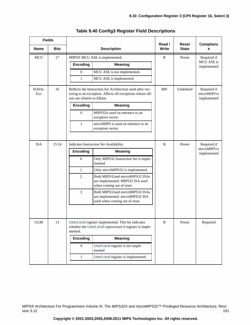
9.33 Configuration Register 3 (CP0 Register 16, Select 3)
MIPS® Architecture For Programmers Volume III: The MIPS32® and microMIPS32™ Privileged Resource Architecture, Revi-sion 3.12 161
Copyright © 2001-2003,2005,2008-2011 MIPS Technologies Inc. All rights reserved.
MCU 17 MIPS® MCU ASE is implemented. R Preset Required ifMCU ASE isimplemented
ISAOn-Exc
16 Reflects the Instruction Set Architecture used after vec-toring to an exception. Affects all exceptions whose off-sets are relative to EBase.
RW Undefined Required ifmicroMIPS isimplemented
ISA 15:14 Indicates Instruction Set Availability. R Preset Required ifmicroMIPS isimplemented
ULRI 13 UserLocal register implemented. This bit indicateswhether the UserLocal coprocessor 0 register is imple-mented.
R Preset Required
Table 9.40 Config3 Register Field Descriptions
Fields
DescriptionRead /Write
ResetState
ComplianceName Bits
Encoding Meaning
0 MCU ASE is not implemented.
1 MCU ASE is implemented
Encoding Meaning
0 MIPS32is used on entrance to anexception vector.
1 microMIPS is used on entrance to anexception vector.
Encoding Meaning
0 Only MIPS32 Instruction Set is imple-mented.
1 Only microMIPS32 is implemented.
2 Both MIPS32and microMIPS32 ISAsare implemented. MIPS32 ISA usedwhen coming out of reset.
3 Both MIPS32and microMIPS32 ISAsare implemented. microMIPS32 ISAused when coming out of reset.
Encoding Meaning
0 UserLocal register is not imple-mented
1 UserLocal register is implemented
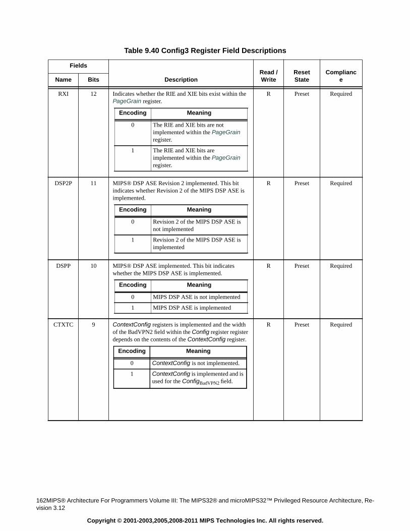
162MIPS® Architecture For Programmers Volume III: The MIPS32® and microMIPS32™ Privileged Resource Architecture, Re-vision 3.12
Copyright © 2001-2003,2005,2008-2011 MIPS Technologies Inc. All rights reserved.
RXI 12 Indicates whether the RIE and XIE bits exist within thePageGrain register.
R Preset Required
DSP2P 11 MIPS® DSP ASE Revision 2 implemented. This bitindicates whether Revision 2 of the MIPS DSP ASE isimplemented.
R Preset Required
DSPP 10 MIPS® DSP ASE implemented. This bit indicateswhether the MIPS DSP ASE is implemented.
R Preset Required
CTXTC 9 ContextConfig registers is implemented and the widthof the BadVPN2 field within the Config register registerdepends on the contents of the ContextConfig register.
R Preset Required
Table 9.40 Config3 Register Field Descriptions
Fields
DescriptionRead /Write
ResetState
ComplianceName Bits
Encoding Meaning
0 The RIE and XIE bits are notimplemented within the PageGrainregister.
1 The RIE and XIE bits areimplemented within the PageGrainregister.
Encoding Meaning
0 Revision 2 of the MIPS DSP ASE isnot implemented
1 Revision 2 of the MIPS DSP ASE isimplemented
Encoding Meaning
0 MIPS DSP ASE is not implemented
1 MIPS DSP ASE is implemented
Encoding Meaning
0 ContextConfig is not implemented.
1 ContextConfig is implemented and isused for the ConfigBadVPN2 field.
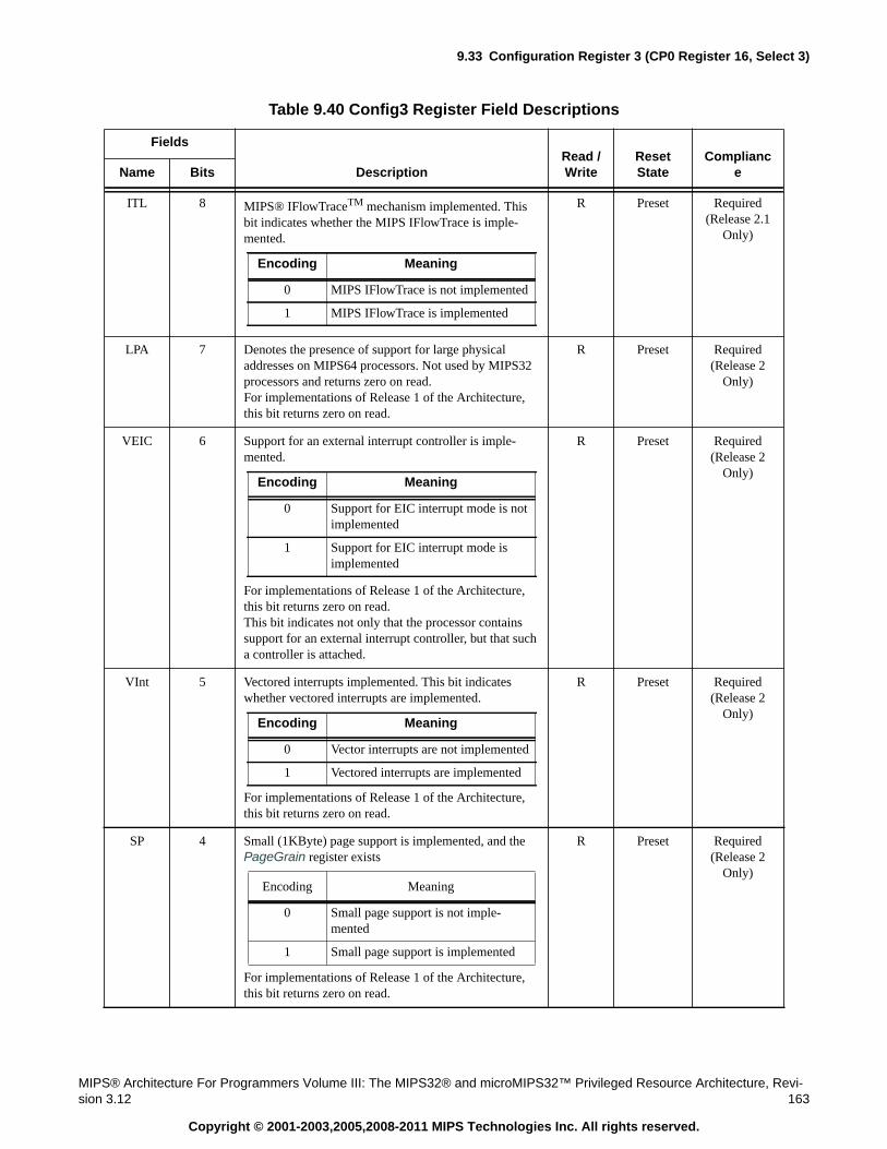
9.33 Configuration Register 3 (CP0 Register 16, Select 3)
MIPS® Architecture For Programmers Volume III: The MIPS32® and microMIPS32™ Privileged Resource Architecture, Revi-sion 3.12 163
Copyright © 2001-2003,2005,2008-2011 MIPS Technologies Inc. All rights reserved.
ITL 8 MIPS® IFlowTraceTM mechanism implemented. Thisbit indicates whether the MIPS IFlowTrace is imple-mented.
R Preset Required(Release 2.1
Only)
LPA 7 Denotes the presence of support for large physicaladdresses on MIPS64 processors. Not used by MIPS32processors and returns zero on read.For implementations of Release 1 of the Architecture,this bit returns zero on read.
R Preset Required(Release 2
Only)
VEIC 6 Support for an external interrupt controller is imple-mented.
For implementations of Release 1 of the Architecture,this bit returns zero on read.This bit indicates not only that the processor containssupport for an external interrupt controller, but that sucha controller is attached.
R Preset Required(Release 2
Only)
VInt 5 Vectored interrupts implemented. This bit indicateswhether vectored interrupts are implemented.
For implementations of Release 1 of the Architecture,this bit returns zero on read.
R Preset Required(Release 2
Only)
SP 4 Small (1KByte) page support is implemented, and thePageGrain register exists
For implementations of Release 1 of the Architecture,this bit returns zero on read.
R Preset Required(Release 2
Only)
Table 9.40 Config3 Register Field Descriptions
Fields
DescriptionRead /Write
ResetState
ComplianceName Bits
Encoding Meaning
0 MIPS IFlowTrace is not implemented
1 MIPS IFlowTrace is implemented
Encoding Meaning
0 Support for EIC interrupt mode is notimplemented
1 Support for EIC interrupt mode isimplemented
Encoding Meaning
0 Vector interrupts are not implemented
1 Vectored interrupts are implemented
Encoding Meaning
0 Small page support is not imple-mented
1 Small page support is implemented
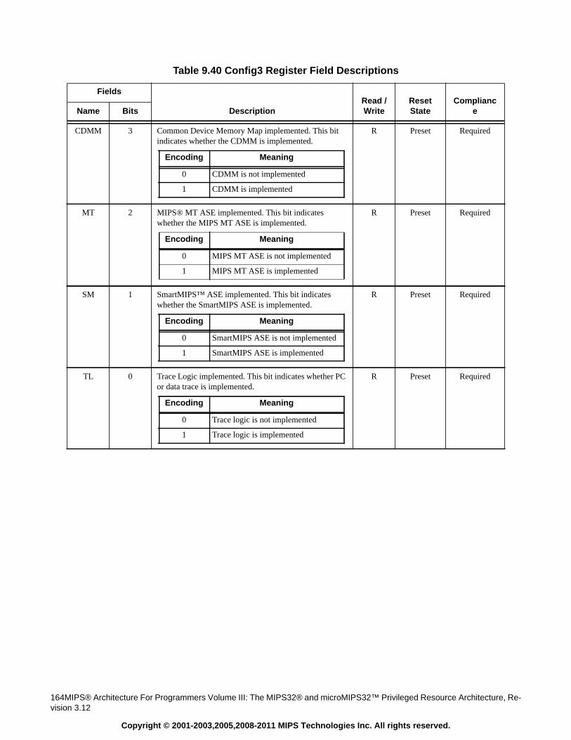
164MIPS® Architecture For Programmers Volume III: The MIPS32® and microMIPS32™ Privileged Resource Architecture, Re-vision 3.12
Copyright © 2001-2003,2005,2008-2011 MIPS Technologies Inc. All rights reserved.
CDMM 3 Common Device Memory Map implemented. This bitindicates whether the CDMM is implemented.
R Preset Required
MT 2 MIPS® MT ASE implemented. This bit indicateswhether the MIPS MT ASE is implemented.
R Preset Required
SM 1 SmartMIPS™ ASE implemented. This bit indicateswhether the SmartMIPS ASE is implemented.
R Preset Required
TL 0 Trace Logic implemented. This bit indicates whether PCor data trace is implemented.
R Preset Required
Table 9.40 Config3 Register Field Descriptions
Fields
DescriptionRead /Write
ResetState
ComplianceName Bits
Encoding Meaning
0 CDMM is not implemented
1 CDMM is implemented
Encoding Meaning
0 MIPS MT ASE is not implemented
1 MIPS MT ASE is implemented
Encoding Meaning
0 SmartMIPS ASE is not implemented
1 SmartMIPS ASE is implemented
Encoding Meaning
0 Trace logic is not implemented
1 Trace logic is implemented
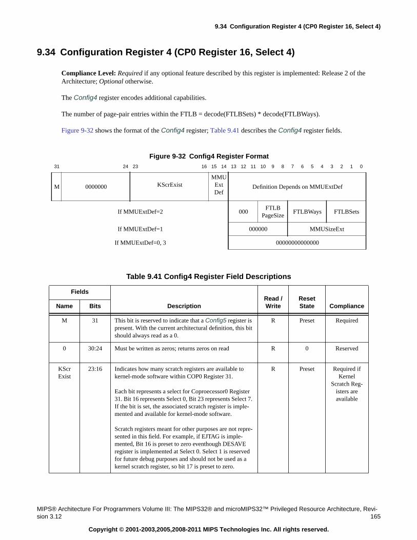
9.34 Configuration Register 4 (CP0 Register 16, Select 4)
MIPS® Architecture For Programmers Volume III: The MIPS32® and microMIPS32™ Privileged Resource Architecture, Revi-sion 3.12 165
Copyright © 2001-2003,2005,2008-2011 MIPS Technologies Inc. All rights reserved.
9.34 Configuration Register 4 (CP0 Register 16, Select 4)
Compliance Level: Required if any optional feature described by this register is implemented: Release 2 of theArchitecture; Optional otherwise.
The Config4 register encodes additional capabilities.
The number of page-pair entries within the FTLB = decode(FTLBSets) * decode(FTLBWays).
Figure 9-32 shows the format of the Config4 register; Table 9.41 describes the Config4 register fields.
Figure 9-32 Config4 Register Format31 24 23 16 15 14 13 12 11 10 9 8 7 6 5 4 3 2 1 0
M 0000000 KScrExistMMU
ExtDef
Definition Depends on MMUExtDef
If MMUExtDef=2 000FTLB
PageSizeFTLBWays FTLBSets
If MMUExtDef=1 000000 MMUSizeExt
If MMUExtDef=0, 3 00000000000000
Table 9.41 Config4 Register Field Descriptions
Fields
DescriptionRead /Write
ResetState ComplianceName Bits
M 31 This bit is reserved to indicate that a Config5 register ispresent. With the current architectural definition, this bitshould always read as a 0.
R Preset Required
0 30:24 Must be written as zeros; returns zeros on read R 0 Reserved
KScrExist
23:16 Indicates how many scratch registers are available tokernel-mode software within COP0 Register 31.
Each bit represents a select for Coproecessor0 Register31. Bit 16 represents Select 0, Bit 23 represents Select 7.If the bit is set, the associated scratch register is imple-mented and available for kernel-mode software.
Scratch registers meant for other purposes are not repre-sented in this field. For example, if EJTAG is imple-mented, Bit 16 is preset to zero eventhough DESAVEregister is implemented at Select 0. Select 1 is reservedfor future debug purposes and should not be used as akernel scratch register, so bit 17 is preset to zero.
R Preset Required ifKernel
Scratch Reg-isters areavailable
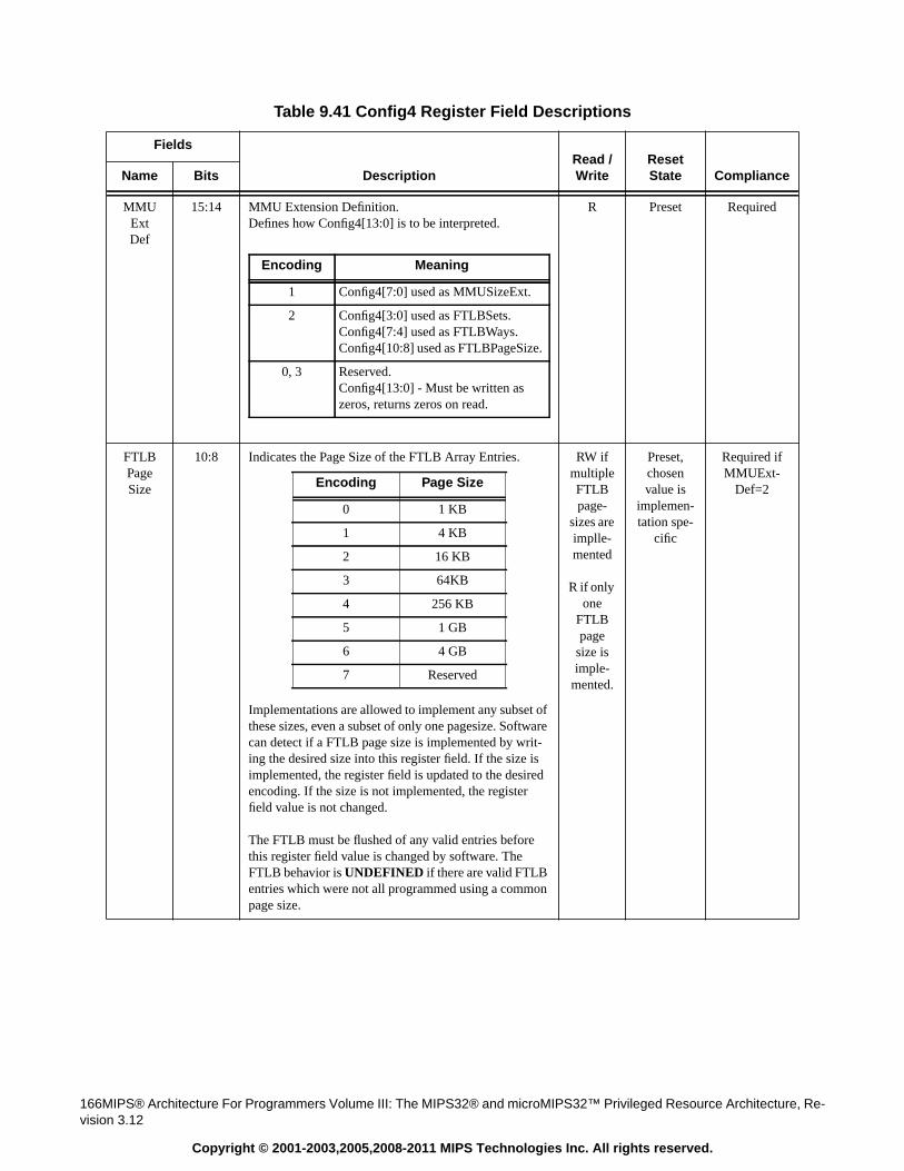
166MIPS® Architecture For Programmers Volume III: The MIPS32® and microMIPS32™ Privileged Resource Architecture, Re-vision 3.12
Copyright © 2001-2003,2005,2008-2011 MIPS Technologies Inc. All rights reserved.
MMUExtDef
15:14 MMU Extension Definition.Defines how Config4[13:0] is to be interpreted.
R Preset Required
FTLBPageSize
10:8 Indicates the Page Size of the FTLB Array Entries.
Implementations are allowed to implement any subset ofthese sizes, even a subset of only one pagesize. Softwarecan detect if a FTLB page size is implemented by writ-ing the desired size into this register field. If the size isimplemented, the register field is updated to the desiredencoding. If the size is not implemented, the registerfield value is not changed.
The FTLB must be flushed of any valid entries beforethis register field value is changed by software. TheFTLB behavior is UNDEFINED if there are valid FTLBentries which were not all programmed using a commonpage size.
RW ifmultipleFTLBpage-
sizes areimplle-mented
R if onlyone
FTLBpage
size isimple-
mented.
Preset,chosenvalue is
implemen-tation spe-
cific
Required ifMMUExt-
Def=2
Table 9.41 Config4 Register Field Descriptions
Fields
DescriptionRead /Write
ResetState ComplianceName Bits
Encoding Meaning
1 Config4[7:0] used as MMUSizeExt.
2 Config4[3:0] used as FTLBSets.Config4[7:4] used as FTLBWays.Config4[10:8] used as FTLBPageSize.
0, 3 Reserved.Config4[13:0] - Must be written aszeros, returns zeros on read.
Encoding Page Size
0 1 KB
1 4 KB
2 16 KB
3 64KB
4 256 KB
5 1 GB
6 4 GB
7 Reserved
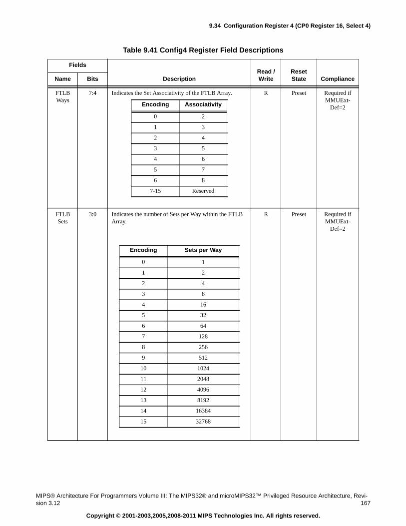
9.34 Configuration Register 4 (CP0 Register 16, Select 4)
MIPS® Architecture For Programmers Volume III: The MIPS32® and microMIPS32™ Privileged Resource Architecture, Revi-sion 3.12 167
Copyright © 2001-2003,2005,2008-2011 MIPS Technologies Inc. All rights reserved.
FTLBWays
7:4 Indicates the Set Associativity of the FTLB Array. R Preset Required ifMMUExt-
Def=2
FTLBSets
3:0 Indicates the number of Sets per Way within the FTLBArray.
R Preset Required ifMMUExt-
Def=2
Table 9.41 Config4 Register Field Descriptions
Fields
DescriptionRead /Write
ResetState ComplianceName Bits
Encoding Associativity
0 2
1 3
2 4
3 5
4 6
5 7
6 8
7-15 Reserved
Encoding Sets per Way
0 1
1 2
2 4
3 8
4 16
5 32
6 64
7 128
8 256
9 512
10 1024
11 2048
12 4096
13 8192
14 16384
15 32768
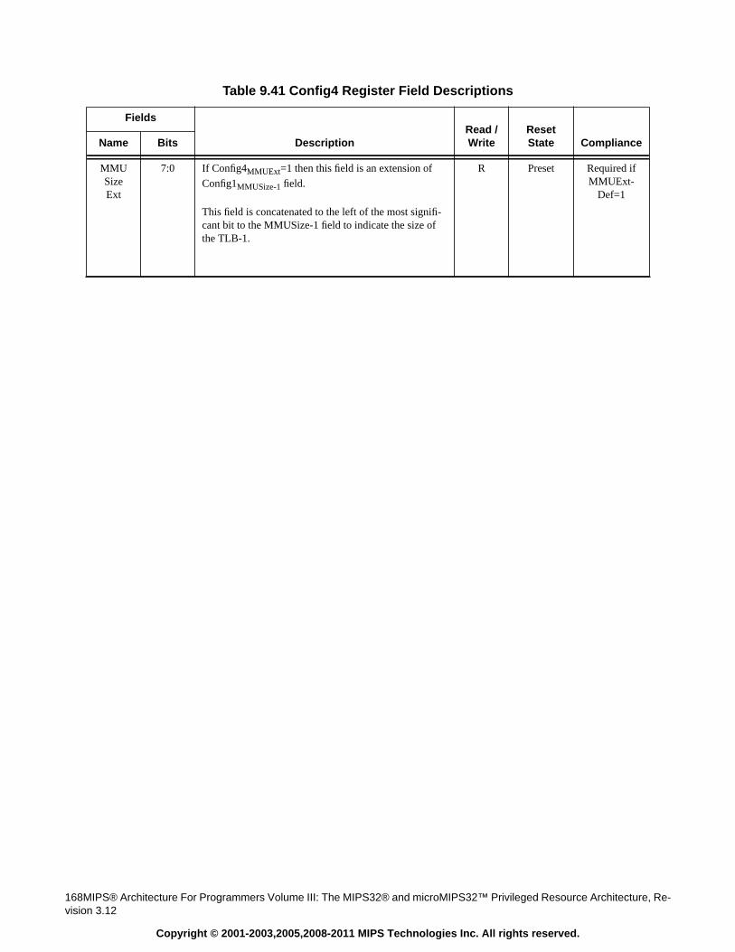
168MIPS® Architecture For Programmers Volume III: The MIPS32® and microMIPS32™ Privileged Resource Architecture, Re-vision 3.12
Copyright © 2001-2003,2005,2008-2011 MIPS Technologies Inc. All rights reserved.
MMUSizeExt
7:0 If Config4MMUExt=1 then this field is an extension of
Config1MMUSize-1 field.
This field is concatenated to the left of the most signifi-cant bit to the MMUSize-1 field to indicate the size ofthe TLB-1.
R Preset Required ifMMUExt-
Def=1
Table 9.41 Config4 Register Field Descriptions
Fields
DescriptionRead /Write
ResetState ComplianceName Bits
9.35 Reserved for Implementations (CP0 Register 16, Selects 6 and 7)
MIPS® Architecture For Programmers Volume III: The MIPS32® and microMIPS32™ Privileged Resource Architecture, Revi-sion 3.12 169
Copyright © 2001-2003,2005,2008-2011 MIPS Technologies Inc. All rights reserved.
9.35 Reserved for Implementations (CP0 Register 16, Selects 6 and 7)
Compliance Level: Implementation Dependent.
CP0 register 16, Selects 6 and 7 are reserved for implementation dependent use and is not defined by the architecture.In order to use CP0 register 16, Selects 6 and 7, it is not necessary to implement CP0 register 16, Selects 2 through 5only to set the M bit in each of these registers. That is, if the Config2 and Config3 registers are not needed for theimplementation, they need not be implemented just to provide the M bits.
The architecture only defines the use of the M bits for presence detection of Selects 1 to 5.
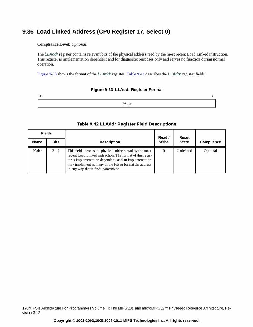
170MIPS® Architecture For Programmers Volume III: The MIPS32® and microMIPS32™ Privileged Resource Architecture, Re-vision 3.12
Copyright © 2001-2003,2005,2008-2011 MIPS Technologies Inc. All rights reserved.
9.36 Load Linked Address (CP0 Register 17, Select 0)
Compliance Level: Optional.
The LLAddr register contains relevant bits of the physical address read by the most recent Load Linked instruction.This register is implementation dependent and for diagnostic purposes only and serves no function during normaloperation.
Figure 9-33 shows the format of the LLAddr register; Table 9.42 describes the LLAddr register fields.
Figure 9-33 LLAddr Register Format31 0
PAddr
Table 9.42 LLAddr Register Field Descriptions
Fields
DescriptionRead /Write
ResetState ComplianceName Bits
PAddr 31..0 This field encodes the physical address read by the mostrecent Load Linked instruction. The format of this regis-ter is implementation dependent, and an implementationmay implement as many of the bits or format the addressin any way that it finds convenient.
R Undefined Optional
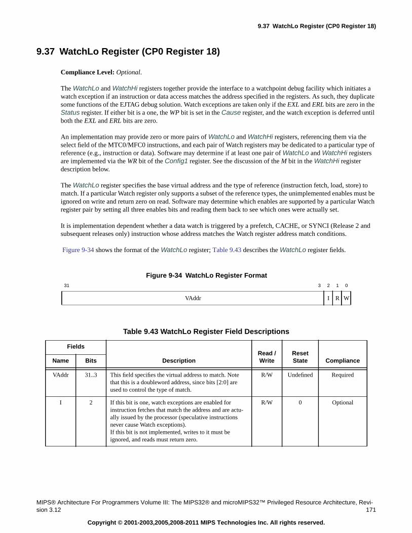
9.37 WatchLo Register (CP0 Register 18)
MIPS® Architecture For Programmers Volume III: The MIPS32® and microMIPS32™ Privileged Resource Architecture, Revi-sion 3.12 171
Copyright © 2001-2003,2005,2008-2011 MIPS Technologies Inc. All rights reserved.
9.37 WatchLo Register (CP0 Register 18)
Compliance Level: Optional.
The WatchLo and WatchHi registers together provide the interface to a watchpoint debug facility which initiates awatch exception if an instruction or data access matches the address specified in the registers. As such, they duplicatesome functions of the EJTAG debug solution. Watch exceptions are taken only if the EXL and ERL bits are zero in theStatus register. If either bit is a one, the WP bit is set in the Cause register, and the watch exception is deferred untilboth the EXL and ERL bits are zero.
An implementation may provide zero or more pairs of WatchLo and WatchHi registers, referencing them via theselect field of the MTC0/MFC0 instructions, and each pair of Watch registers may be dedicated to a particular type ofreference (e.g., instruction or data). Software may determine if at least one pair of WatchLo and WatchHi registersare implemented via the WR bit of the Config1 register. See the discussion of the M bit in the WatchHi registerdescription below.
The WatchLo register specifies the base virtual address and the type of reference (instruction fetch, load, store) tomatch. If a particular Watch register only supports a subset of the reference types, the unimplemented enables must beignored on write and return zero on read. Software may determine which enables are supported by a particular Watchregister pair by setting all three enables bits and reading them back to see which ones were actually set.
It is implementation dependent whether a data watch is triggered by a prefetch, CACHE, or SYNCI (Release 2 andsubsequent releases only) instruction whose address matches the Watch register address match conditions.
Figure 9-34 shows the format of the WatchLo register; Table 9.43 describes the WatchLo register fields.
Figure 9-34 WatchLo Register Format31 3 2 1 0
VAddr I R W
Table 9.43 WatchLo Register Field Descriptions
Fields
DescriptionRead /Write
ResetState ComplianceName Bits
VAddr 31..3 This field specifies the virtual address to match. Notethat this is a doubleword address, since bits [2:0] areused to control the type of match.
R/W Undefined Required
I 2 If this bit is one, watch exceptions are enabled forinstruction fetches that match the address and are actu-ally issued by the processor (speculative instructionsnever cause Watch exceptions).If this bit is not implemented, writes to it must beignored, and reads must return zero.
R/W 0 Optional
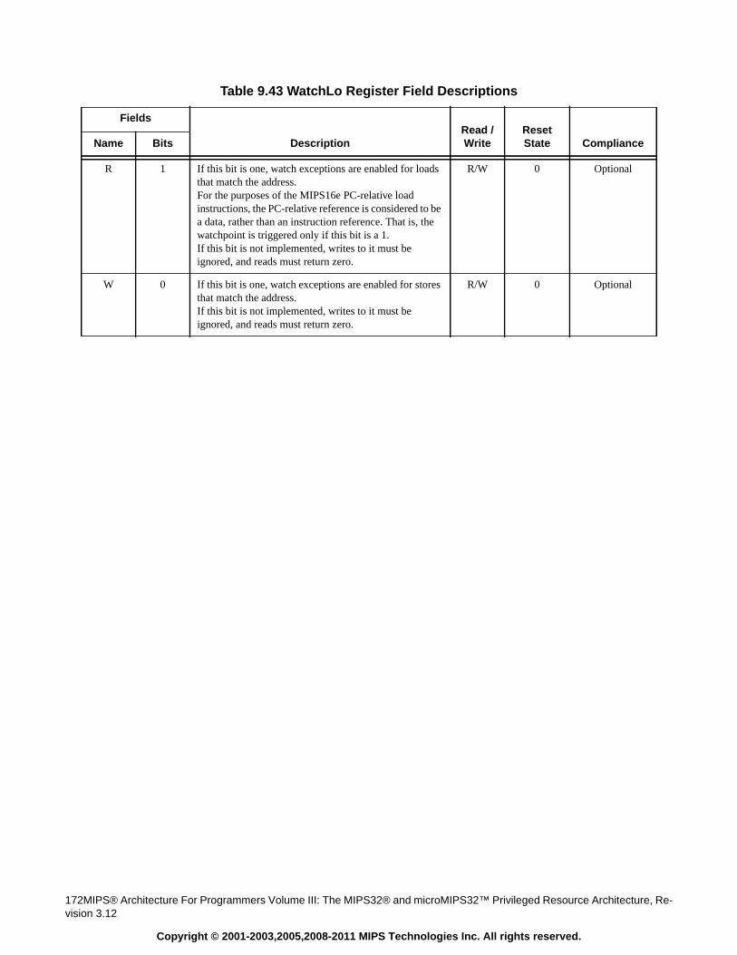
172MIPS® Architecture For Programmers Volume III: The MIPS32® and microMIPS32™ Privileged Resource Architecture, Re-vision 3.12
Copyright © 2001-2003,2005,2008-2011 MIPS Technologies Inc. All rights reserved.
R 1 If this bit is one, watch exceptions are enabled for loadsthat match the address.For the purposes of the MIPS16e PC-relative loadinstructions, the PC-relative reference is considered to bea data, rather than an instruction reference. That is, thewatchpoint is triggered only if this bit is a 1.If this bit is not implemented, writes to it must beignored, and reads must return zero.
R/W 0 Optional
W 0 If this bit is one, watch exceptions are enabled for storesthat match the address.If this bit is not implemented, writes to it must beignored, and reads must return zero.
R/W 0 Optional
Table 9.43 WatchLo Register Field Descriptions
Fields
DescriptionRead /Write
ResetState ComplianceName Bits
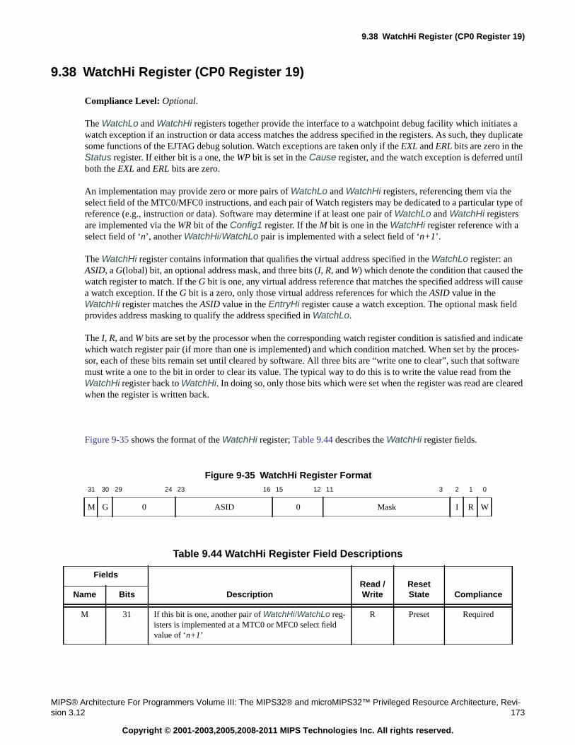
9.38 WatchHi Register (CP0 Register 19)
MIPS® Architecture For Programmers Volume III: The MIPS32® and microMIPS32™ Privileged Resource Architecture, Revi-sion 3.12 173
Copyright © 2001-2003,2005,2008-2011 MIPS Technologies Inc. All rights reserved.
9.38 WatchHi Register (CP0 Register 19)
Compliance Level: Optional.
The WatchLo and WatchHi registers together provide the interface to a watchpoint debug facility which initiates awatch exception if an instruction or data access matches the address specified in the registers. As such, they duplicatesome functions of the EJTAG debug solution. Watch exceptions are taken only if the EXL and ERL bits are zero in theStatus register. If either bit is a one, the WP bit is set in the Cause register, and the watch exception is deferred untilboth the EXL and ERL bits are zero.
An implementation may provide zero or more pairs of WatchLo and WatchHi registers, referencing them via theselect field of the MTC0/MFC0 instructions, and each pair of Watch registers may be dedicated to a particular type ofreference (e.g., instruction or data). Software may determine if at least one pair of WatchLo and WatchHi registersare implemented via the WR bit of the Config1 register. If the M bit is one in the WatchHi register reference with aselect field of ‘n’, another WatchHi/WatchLo pair is implemented with a select field of ‘n+1’.
The WatchHi register contains information that qualifies the virtual address specified in the WatchLo register: anASID, a G(lobal) bit, an optional address mask, and three bits (I, R, and W) which denote the condition that caused thewatch register to match. If the G bit is one, any virtual address reference that matches the specified address will causea watch exception. If the G bit is a zero, only those virtual address references for which the ASID value in theWatchHi register matches the ASID value in the EntryHi register cause a watch exception. The optional mask fieldprovides address masking to qualify the address specified in WatchLo.
The I, R, and W bits are set by the processor when the corresponding watch register condition is satisfied and indicatewhich watch register pair (if more than one is implemented) and which condition matched. When set by the proces-sor, each of these bits remain set until cleared by software. All three bits are “write one to clear”, such that softwaremust write a one to the bit in order to clear its value. The typical way to do this is to write the value read from theWatchHi register back to WatchHi. In doing so, only those bits which were set when the register was read are clearedwhen the register is written back.
Figure 9-35 shows the format of the WatchHi register; Table 9.44 describes the WatchHi register fields.
Figure 9-35 WatchHi Register Format31 30 29 24 23 16 15 12 11 3 2 1 0
M G 0 ASID 0 Mask I R W
Table 9.44 WatchHi Register Field Descriptions
Fields
DescriptionRead /Write
ResetState ComplianceName Bits
M 31 If this bit is one, another pair of WatchHi/WatchLo reg-isters is implemented at a MTC0 or MFC0 select fieldvalue of ‘n+1’
R Preset Required
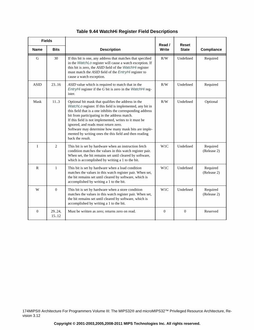
174MIPS® Architecture For Programmers Volume III: The MIPS32® and microMIPS32™ Privileged Resource Architecture, Re-vision 3.12
Copyright © 2001-2003,2005,2008-2011 MIPS Technologies Inc. All rights reserved.
G 30 If this bit is one, any address that matches that specifiedin the WatchLo register will cause a watch exception. Ifthis bit is zero, the ASID field of the WatchHi registermust match the ASID field of the EntryHi register tocause a watch exception.
R/W Undefined Required
ASID 23..16 ASID value which is required to match that in theEntryHi register if the G bit is zero in the WatchHi reg-ister.
R/W Undefined Required
Mask 11..3 Optional bit mask that qualifies the address in theWatchLo register. If this field is implemented, any bit inthis field that is a one inhibits the corresponding addressbit from participating in the address match.If this field is not implemented, writes to it must beignored, and reads must return zero.Software may determine how many mask bits are imple-mented by writing ones the this field and then readingback the result.
R/W Undefined Optional
I 2 This bit is set by hardware when an instruction fetchcondition matches the values in this watch register pair.When set, the bit remains set until cleared by software,which is accomplished by writing a 1 to the bit.
W1C Undefined Required(Release 2)
R 1 This bit is set by hardware when a load conditionmatches the values in this watch register pair. When set,the bit remains set until cleared by software, which isaccomplished by writing a 1 to the bit.
W1C Undefined Required(Release 2)
W 0 This bit is set by hardware when a store conditionmatches the values in this watch register pair. When set,the bit remains set until cleared by software, which isaccomplished by writing a 1 to the bit.
W1C Undefined Required(Release 2)
0 29..24,15..12
Must be written as zero; returns zero on read. 0 0 Reserved
Table 9.44 WatchHi Register Field Descriptions
Fields
DescriptionRead /Write
ResetState ComplianceName Bits
9.39 Reserved for Implementations (CP0 Register 22, all Select values)
MIPS® Architecture For Programmers Volume III: The MIPS32® and microMIPS32™ Privileged Resource Architecture, Revi-sion 3.12 175
Copyright © 2001-2003,2005,2008-2011 MIPS Technologies Inc. All rights reserved.
9.39 Reserved for Implementations (CP0 Register 22, all Select values)
Compliance Level: Implementation Dependent.
CP0 register 22 is reserved for implementation dependent use and is not defined by the architecture.
176MIPS® Architecture For Programmers Volume III: The MIPS32® and microMIPS32™ Privileged Resource Architecture, Re-vision 3.12
Copyright © 2001-2003,2005,2008-2011 MIPS Technologies Inc. All rights reserved.
9.40 Debug Register (CP0 Register 23, Select 0 )
Compliance Level: Optional.
The Debug register is part of the EJTAG specification. Refer to that specification for the format and description ofthis register.

9.40 Debug Register (CP0 Register 23, Select 0 )
MIPS® Architecture For Programmers Volume III: The MIPS32® and microMIPS32™ Privileged Resource Architecture, Revi-sion 3.12 177
Copyright © 2001-2003,2005,2008-2011 MIPS Technologies Inc. All rights reserved.

178MIPS® Architecture For Programmers Volume III: The MIPS32® and microMIPS32™ Privileged Resource Architecture, Re-vision 3.12
Copyright © 2001-2003,2005,2008-2011 MIPS Technologies Inc. All rights reserved.
9.41 Debug2 Register (CP0 Register 23, Select 6)
Compliance Level: Optional.
The Debug2 register is part of the EJTAG specification. Refer to that specification for the format and description ofthis register.
9.42 DEPC Register (CP0 Register 24)
MIPS® Architecture For Programmers Volume III: The MIPS32® and microMIPS32™ Privileged Resource Architecture, Revi-sion 3.12 179
Copyright © 2001-2003,2005,2008-2011 MIPS Technologies Inc. All rights reserved.
9.42 DEPC Register (CP0 Register 24)
Compliance Level: Optional.
The DEPC register is a read-write register that contains the address at which processing resumes after a debug excep-tion has been serviced. It is part of the EJTAG specification and the reader is referred there for the format and descrip-tion of the register. All bits of the DEPC register are significant and must be writable.
When a debug exception occurs, the processor writes the DEPC register with,
• the virtual address of the instruction that was the direct cause of the exception, or
• the virtual address of the immediately preceding branch or jump instruction, when the exception causing instruc-tion is in a branch delay slot, and the Branch Delay bit in the Cause register is set.
The processor reads the DEPC register as the result of execution of the DERET instruction.
Software may write the DEPC register to change the processor resume address and read the DEPC register to deter-mine at what address the processor will resume.
9.42.1 Special Handling of the DEPC Register in Processors That Implement theMIPS16e ASE or microMIPS32 Base Architecture
In processors that implement the MIPS16e ASE or the microMIPS32 base architecture, the DEPC register requiresspecial handling.
When the processor writes the DEPC register, it combines the address at which processing resumes with the value ofthe ISA Mode register:
DEPC ← resumePC31..1 || ISAMode0
“resumePC” is the address at which processing resumes, as described above.
When the processor reads the DEPC register, it distributes the bits to the PC and ISA Mode registers:
PC ← DEPC31..1 || 0ISAMode ← DEPC0
Software reads of the DEPC register simply return to a GPR the last value written with no interpretation. Softwarewrites to the DEPC register store a new value which is interpreted by the processor as described above.
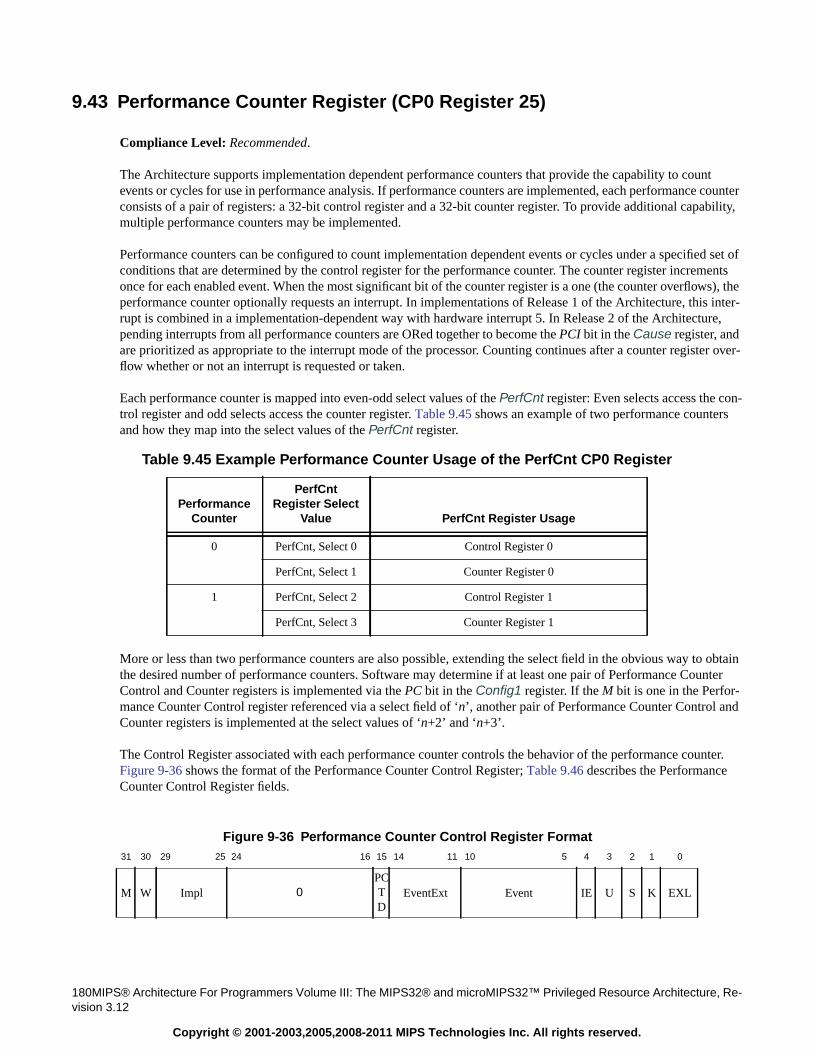
180MIPS® Architecture For Programmers Volume III: The MIPS32® and microMIPS32™ Privileged Resource Architecture, Re-vision 3.12
Copyright © 2001-2003,2005,2008-2011 MIPS Technologies Inc. All rights reserved.
9.43 Performance Counter Register (CP0 Register 25)
Compliance Level: Recommended.
The Architecture supports implementation dependent performance counters that provide the capability to countevents or cycles for use in performance analysis. If performance counters are implemented, each performance counterconsists of a pair of registers: a 32-bit control register and a 32-bit counter register. To provide additional capability,multiple performance counters may be implemented.
Performance counters can be configured to count implementation dependent events or cycles under a specified set ofconditions that are determined by the control register for the performance counter. The counter register incrementsonce for each enabled event. When the most significant bit of the counter register is a one (the counter overflows), theperformance counter optionally requests an interrupt. In implementations of Release 1 of the Architecture, this inter-rupt is combined in a implementation-dependent way with hardware interrupt 5. In Release 2 of the Architecture,pending interrupts from all performance counters are ORed together to become the PCI bit in the Cause register, andare prioritized as appropriate to the interrupt mode of the processor. Counting continues after a counter register over-flow whether or not an interrupt is requested or taken.
Each performance counter is mapped into even-odd select values of the PerfCnt register: Even selects access the con-trol register and odd selects access the counter register. Table 9.45 shows an example of two performance countersand how they map into the select values of the PerfCnt register.
More or less than two performance counters are also possible, extending the select field in the obvious way to obtainthe desired number of performance counters. Software may determine if at least one pair of Performance CounterControl and Counter registers is implemented via the PC bit in the Config1 register. If the M bit is one in the Perfor-mance Counter Control register referenced via a select field of ‘n’, another pair of Performance Counter Control andCounter registers is implemented at the select values of ‘n+2’ and ‘n+3’.
The Control Register associated with each performance counter controls the behavior of the performance counter.Figure 9-36 shows the format of the Performance Counter Control Register; Table 9.46 describes the PerformanceCounter Control Register fields.
Table 9.45 Example Performance Counter Usage of the PerfCnt CP0 Register
PerformanceCounter
PerfCntRegister Select
Value PerfCnt Register Usage
0 PerfCnt, Select 0 Control Register 0
PerfCnt, Select 1 Counter Register 0
1 PerfCnt, Select 2 Control Register 1
PerfCnt, Select 3 Counter Register 1
Figure 9-36 Performance Counter Control Register Format31 30 29 25 24 16 15 14 11 10 5 4 3 2 1 0
M W Impl 0PCTD
EventExt Event IE U S K EXL
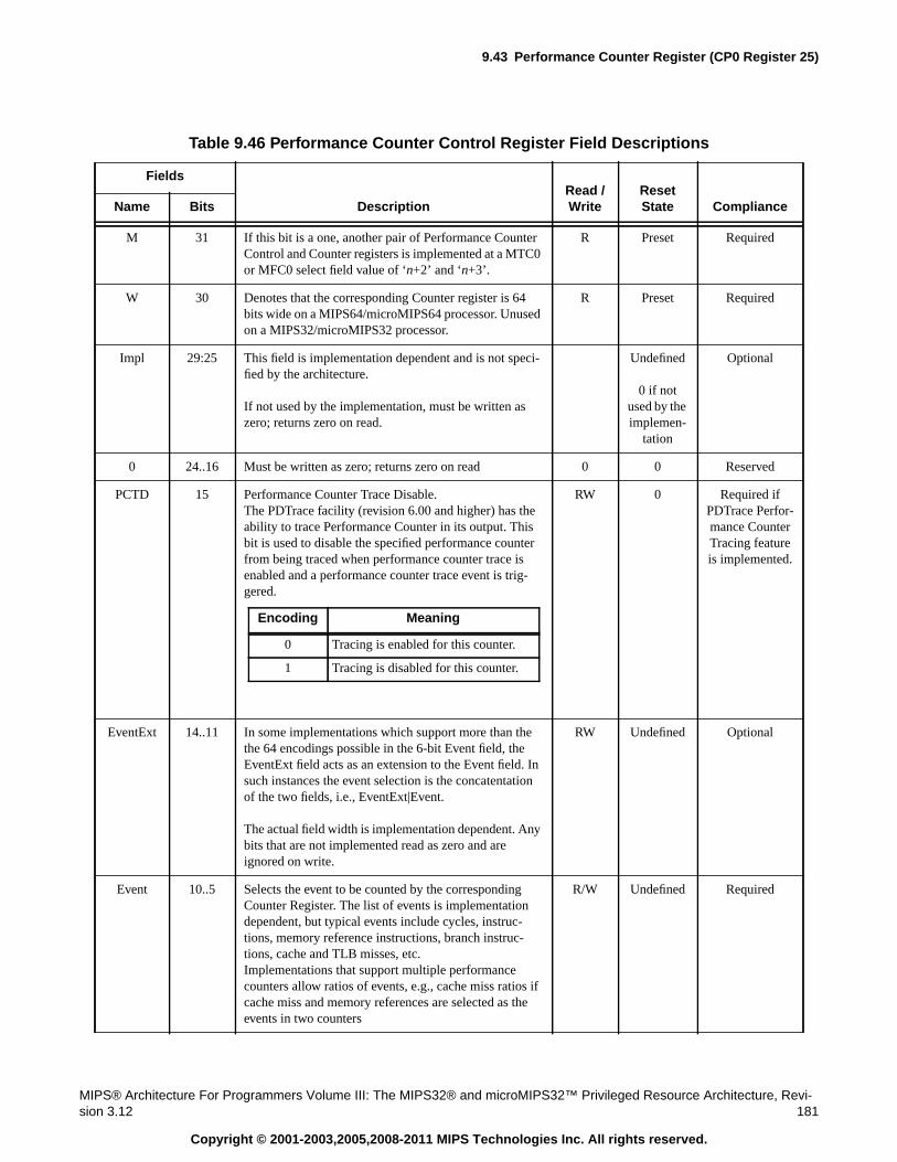
9.43 Performance Counter Register (CP0 Register 25)
MIPS® Architecture For Programmers Volume III: The MIPS32® and microMIPS32™ Privileged Resource Architecture, Revi-sion 3.12 181
Copyright © 2001-2003,2005,2008-2011 MIPS Technologies Inc. All rights reserved.
Table 9.46 Performance Counter Control Register Field Descriptions
Fields
DescriptionRead /Write
ResetState ComplianceName Bits
M 31 If this bit is a one, another pair of Performance CounterControl and Counter registers is implemented at a MTC0or MFC0 select field value of ‘n+2’ and ‘n+3’.
R Preset Required
W 30 Denotes that the corresponding Counter register is 64bits wide on a MIPS64/microMIPS64 processor. Unusedon a MIPS32/microMIPS32 processor.
R Preset Required
Impl 29:25 This field is implementation dependent and is not speci-fied by the architecture.
If not used by the implementation, must be written aszero; returns zero on read.
Undefined
0 if notused by theimplemen-
tation
Optional
0 24..16 Must be written as zero; returns zero on read 0 0 Reserved
PCTD 15 Performance Counter Trace Disable.The PDTrace facility (revision 6.00 and higher) has theability to trace Performance Counter in its output. Thisbit is used to disable the specified performance counterfrom being traced when performance counter trace isenabled and a performance counter trace event is trig-gered.
RW 0 Required ifPDTrace Perfor-mance CounterTracing featureis implemented.
EventExt 14..11 In some implementations which support more than thethe 64 encodings possible in the 6-bit Event field, theEventExt field acts as an extension to the Event field. Insuch instances the event selection is the concatentationof the two fields, i.e., EventExt|Event.
The actual field width is implementation dependent. Anybits that are not implemented read as zero and areignored on write.
RW Undefined Optional
Event 10..5 Selects the event to be counted by the correspondingCounter Register. The list of events is implementationdependent, but typical events include cycles, instruc-tions, memory reference instructions, branch instruc-tions, cache and TLB misses, etc.Implementations that support multiple performancecounters allow ratios of events, e.g., cache miss ratios ifcache miss and memory references are selected as theevents in two counters
R/W Undefined Required
Encoding Meaning
0 Tracing is enabled for this counter.
1 Tracing is disabled for this counter.
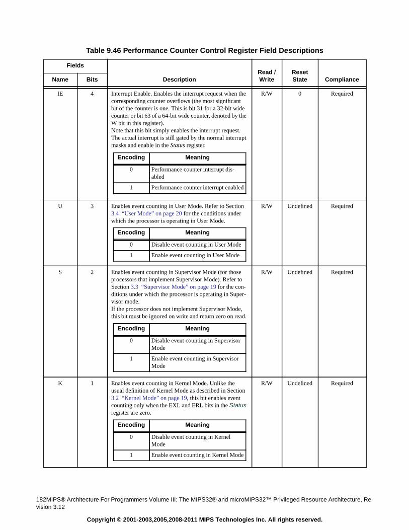
182MIPS® Architecture For Programmers Volume III: The MIPS32® and microMIPS32™ Privileged Resource Architecture, Re-vision 3.12
Copyright © 2001-2003,2005,2008-2011 MIPS Technologies Inc. All rights reserved.
IE 4 Interrupt Enable. Enables the interrupt request when thecorresponding counter overflows (the most significantbit of the counter is one. This is bit 31 for a 32-bit widecounter or bit 63 of a 64-bit wide counter, denoted by theW bit in this register).Note that this bit simply enables the interrupt request.The actual interrupt is still gated by the normal interruptmasks and enable in the Status register.
R/W 0 Required
U 3 Enables event counting in User Mode. Refer to Section3.4 “User Mode” on page 20 for the conditions underwhich the processor is operating in User Mode.
R/W Undefined Required
S 2 Enables event counting in Supervisor Mode (for thoseprocessors that implement Supervisor Mode). Refer toSection 3.3 “Supervisor Mode” on page 19 for the con-ditions under which the processor is operating in Super-visor mode.If the processor does not implement Supervisor Mode,this bit must be ignored on write and return zero on read.
R/W Undefined Required
K 1 Enables event counting in Kernel Mode. Unlike theusual definition of Kernel Mode as described in Section3.2 “Kernel Mode” on page 19, this bit enables eventcounting only when the EXL and ERL bits in the Statusregister are zero.
R/W Undefined Required
Table 9.46 Performance Counter Control Register Field Descriptions
Fields
DescriptionRead /Write
ResetState ComplianceName Bits
Encoding Meaning
0 Performance counter interrupt dis-abled
1 Performance counter interrupt enabled
Encoding Meaning
0 Disable event counting in User Mode
1 Enable event counting in User Mode
Encoding Meaning
0 Disable event counting in SupervisorMode
1 Enable event counting in SupervisorMode
Encoding Meaning
0 Disable event counting in KernelMode
1 Enable event counting in Kernel Mode
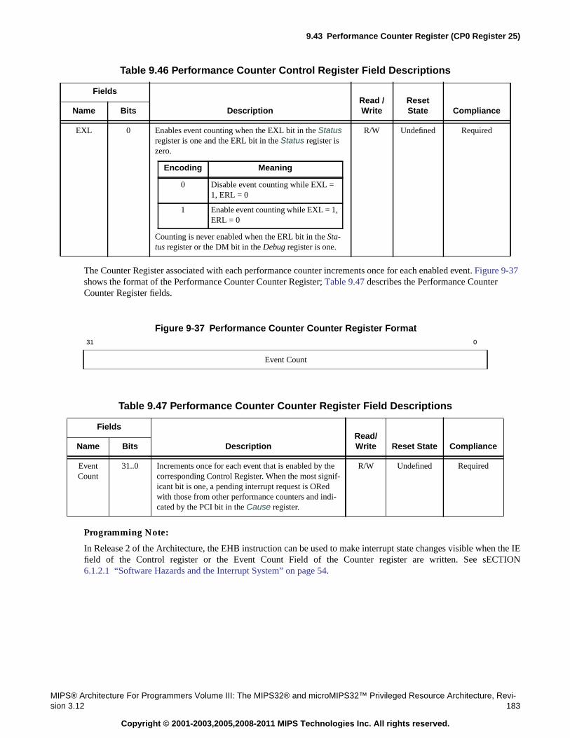
9.43 Performance Counter Register (CP0 Register 25)
MIPS® Architecture For Programmers Volume III: The MIPS32® and microMIPS32™ Privileged Resource Architecture, Revi-sion 3.12 183
Copyright © 2001-2003,2005,2008-2011 MIPS Technologies Inc. All rights reserved.
The Counter Register associated with each performance counter increments once for each enabled event. Figure 9-37shows the format of the Performance Counter Counter Register; Table 9.47 describes the Performance CounterCounter Register fields.
Programming Note:
In Release 2 of the Architecture, the EHB instruction can be used to make interrupt state changes visible when the IEfield of the Control register or the Event Count Field of the Counter register are written. See sECTION6.1.2.1 “Software Hazards and the Interrupt System” on page 54.
EXL 0 Enables event counting when the EXL bit in the Statusregister is one and the ERL bit in the Status register iszero.
Counting is never enabled when the ERL bit in the Sta-tus register or the DM bit in the Debug register is one.
R/W Undefined Required
Figure 9-37 Performance Counter Counter Register Format31 0
Event Count
Table 9.47 Performance Counter Counter Register Field Descriptions
Fields
DescriptionRead/Write Reset State ComplianceName Bits
EventCount
31..0 Increments once for each event that is enabled by thecorresponding Control Register. When the most signif-icant bit is one, a pending interrupt request is ORedwith those from other performance counters and indi-cated by the PCI bit in the Cause register.
R/W Undefined Required
Table 9.46 Performance Counter Control Register Field Descriptions
Fields
DescriptionRead /Write
ResetState ComplianceName Bits
Encoding Meaning
0 Disable event counting while EXL =1, ERL = 0
1 Enable event counting while EXL = 1,ERL = 0
184MIPS® Architecture For Programmers Volume III: The MIPS32® and microMIPS32™ Privileged Resource Architecture, Re-vision 3.12
Copyright © 2001-2003,2005,2008-2011 MIPS Technologies Inc. All rights reserved.
9.44 ErrCtl Register (CP0 Register 26, Select 0)
Compliance Level: Optional.
The ErrCtl register provides an implementation dependent diagnostic interface with the error detection mechanismsimplemented by the processor. This register has been used in previous implementations to read and write parity orECC information to and from the primary or secondary cache data arrays in conjunction with specific encodings ofthe Cache instruction or other implementation-dependent method. The exact format of the ErrCtl register is imple-mentation dependent and not specified by the architecture. Refer to the processor specification for the format of thisregister and a description of the fields.
9.45 CacheErr Register (CP0 Register 27, Select 0)
MIPS® Architecture For Programmers Volume III: The MIPS32® and microMIPS32™ Privileged Resource Architecture, Revi-sion 3.12 185
Copyright © 2001-2003,2005,2008-2011 MIPS Technologies Inc. All rights reserved.
9.45 CacheErr Register (CP0 Register 27, Select 0)
Compliance Level: Optional.
The CacheErr register provides an interface with the cache error detection logic that may be implemented by a pro-cessor.
The exact format of the CacheErr register is implementation dependent and not specified by the architecture. Referto the processor specification for the format of this register and a description of the fields.
186MIPS® Architecture For Programmers Volume III: The MIPS32® and microMIPS32™ Privileged Resource Architecture, Re-vision 3.12
Copyright © 2001-2003,2005,2008-2011 MIPS Technologies Inc. All rights reserved.
9.46 TagLo Register (CP0 Register 28, Select 0, 2)
Compliance Level: Required if a cache is implemented; Optional otherwise.
The TagLo and TagHi registers are read/write registers that act as the interface to the cache tag array. The Index StoreTag and Index Load Tag operations of the CACHE instruction use the TagLo and TagHi registers as the source orsink of tag information, respectively.
The exact format of the TagLo and TagHi registers is implementation dependent. Refer to the processor specificationfor the format of this register and a description of the fields.
However, software must be able to write zeros into the TagLo and TagHi registers and then use the Index Store Tagcache operation to initialize the cache tags to a valid state at powerup.
It is implementation dependent whether there is a single TagLo register that acts as the interface to all caches, or adedicated TagLo register for each cache. If multiple TagLo registers are implemented, they occupy the even selectvalues for this register encoding, with select 0 addressing the instruction cache and select 2 addressing the data cache.Whether individual TagLo registers are implemented or not for each cache, processors must accept a write of zero toselect 0 and select 2 of TagLo as part of the software process of initializing the cache tags at powerup.
9.47 DataLo Register (CP0 Register 28, Select 1, 3)
MIPS® Architecture For Programmers Volume III: The MIPS32® and microMIPS32™ Privileged Resource Architecture, Revi-sion 3.12 187
Copyright © 2001-2003,2005,2008-2011 MIPS Technologies Inc. All rights reserved.
9.47 DataLo Register (CP0 Register 28, Select 1, 3)
Compliance Level: Optional.
The DataLo and DataHi registers are registers that act as the interface to the cache data array and are intended fordiagnostic operation only. The Index Load Tag operation of the CACHE instruction reads the corresponding data val-ues into the DataLo and DataHi registers.
The exact format and operation of the DataLo and DataHi registers is implementation dependent. Refer to the pro-cessor specification for the format of this register and a description of the fields.
It is implementation dependent whether there is a single DataLo register that acts as the interface to all caches, or adedicated DataLo register for each cache. If multiple DataLo registers are implemented, they occupy the odd selectvalues for this register encoding, with select 1 addressing the instruction cache and select 3 addressing the data cache.
188MIPS® Architecture For Programmers Volume III: The MIPS32® and microMIPS32™ Privileged Resource Architecture, Re-vision 3.12
Copyright © 2001-2003,2005,2008-2011 MIPS Technologies Inc. All rights reserved.
9.48 TagHi Register (CP0 Register 29, Select 0, 2)
Compliance Level: Required if a cache is implemented; Optional otherwise.
The TagLo and TagHi registers are read/write registers that act as the interface to the cache tag array. The Index StoreTag and Index Load Tag operations of the CACHE instruction use the TagLo and TagHi registers as the source orsink of tag information, respectively.
The exact format of the TagLo and TagHi registers is implementation dependent. Refer to the processor specificationfor the format of this register and a description of the fields. However, software must be able to write zeros into theTagLo and TagHi registers and the use the Index Store Tag cache operation to initialize the cache tags to a valid stateat powerup.
It is implementation dependent whether there is a single TagHi register that acts as the interface to all caches, or adedicated TagHi register for each cache. If multiple TagHi registers are implemented, they occupy the even select val-ues for this register encoding, with select 0 addressing the instruction cache and select 2 addressing the data cache.Whether individual TagHi registers are implemented or not for each cache, processors must accept a write of zero toselect 0 and select 2 of TagHi as part of the software process of initializing the cache tags at powerup.
9.49 DataHi Register (CP0 Register 29, Select 1, 3)
MIPS® Architecture For Programmers Volume III: The MIPS32® and microMIPS32™ Privileged Resource Architecture, Revi-sion 3.12 189
Copyright © 2001-2003,2005,2008-2011 MIPS Technologies Inc. All rights reserved.
9.49 DataHi Register (CP0 Register 29, Select 1, 3)
Compliance Level: Optional.
The DataLo and DataHi registers are registers that act as the interface to the cache data array and are intended fordiagnostic operation only. The Index Load Tag operation of the CACHE instruction reads the corresponding data val-ues into the DataLo and DataHi registers.
The exact format and operation of the DataLo and DataHi registers is implementation dependent. Refer to the pro-cessor specification for the format of this register and a description of the fields.
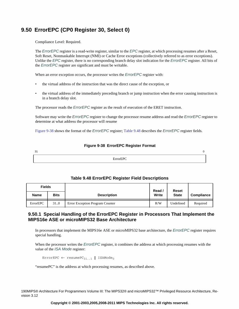
190MIPS® Architecture For Programmers Volume III: The MIPS32® and microMIPS32™ Privileged Resource Architecture, Re-vision 3.12
Copyright © 2001-2003,2005,2008-2011 MIPS Technologies Inc. All rights reserved.
9.50 ErrorEPC (CP0 Register 30, Select 0)
Compliance Level: Required.
The ErrorEPC register is a read-write register, similar to the EPC register, at which processing resumes after a Reset,Soft Reset, Nonmaskable Interrupt (NMI) or Cache Error exceptions (collectively referred to as error exceptions).Unlike the EPC register, there is no corresponding branch delay slot indication for the ErrorEPC register. All bits ofthe ErrorEPC register are significant and must be writable.
When an error exception occurs, the processor writes the ErrorEPC register with:
• the virtual address of the instruction that was the direct cause of the exception, or
• the virtual address of the immediately preceding branch or jump instruction when the error causing instruction isin a branch delay slot.
The processor reads the ErrorEPC register as the result of execution of the ERET instruction.
Software may write the ErrorEPC register to change the processor resume address and read the ErrorEPC register todetermine at what address the processor will resume
Figure 9-38 shows the format of the ErrorEPC register; Table 9.48 describes the ErrorEPC register fields.
9.50.1 Special Handling of the ErrorEPC Register in Processors That Implement theMIPS16e ASE or microMIPS32 Base Architecture
In processors that implement the MIPS16e ASE or microMIPS32 base architecture, the ErrorEPC register requiresspecial handling.
When the processor writes the ErrorEPC register, it combines the address at which processing resumes with thevalue of the ISA Mode register:
ErrorEPC ← resumePC31..1 || ISAMode0
“resumePC” is the address at which processing resumes, as described above.
Figure 9-38 ErrorEPC Register Format31 0
ErrorEPC
Table 9.48 ErrorEPC Register Field Descriptions
Fields
DescriptionRead /Write
ResetState ComplianceName Bits
ErrorEPC 31..0 Error Exception Program Counter R/W Undefined Required
9.50 ErrorEPC (CP0 Register 30, Select 0)
MIPS® Architecture For Programmers Volume III: The MIPS32® and microMIPS32™ Privileged Resource Architecture, Revi-sion 3.12 191
Copyright © 2001-2003,2005,2008-2011 MIPS Technologies Inc. All rights reserved.
When the processor reads the ErrorEPC register, it distributes the bits to the PC and ISAMode registers:
PC ← ErrorEPC31..1 || 0ISAMode ← ErrorEPC0
Software reads of the ErrorEPC register simply return to a GPR the last value written with no interpretation. Soft-ware writes to the ErrorEPC register store a new value which is interpreted by the processor as described above.

192MIPS® Architecture For Programmers Volume III: The MIPS32® and microMIPS32™ Privileged Resource Architecture, Re-vision 3.12
Copyright © 2001-2003,2005,2008-2011 MIPS Technologies Inc. All rights reserved.
9.51 DESAVE Register (CP0 Register 31)
Compliance Level: Optional.
The DESAVE register is part of the EJTAG specification. Refer to that specification for the format and description ofthis register.
The DESAVE register is meant to be used solely while in Debug Mode. If kernel mode software uses this register, itwould conflict with debugging kernel mode software. For that reason, it is strongly recommended that kernel modesoftware not use this register. If the KScratch* registers are implemented, kernel software can use those registers.
9.51 DESAVE Register (CP0 Register 31)
MIPS® Architecture For Programmers Volume III: The MIPS32® and microMIPS32™ Privileged Resource Architecture, Revi-sion 3.12 193
Copyright © 2001-2003,2005,2008-2011 MIPS Technologies Inc. All rights reserved.
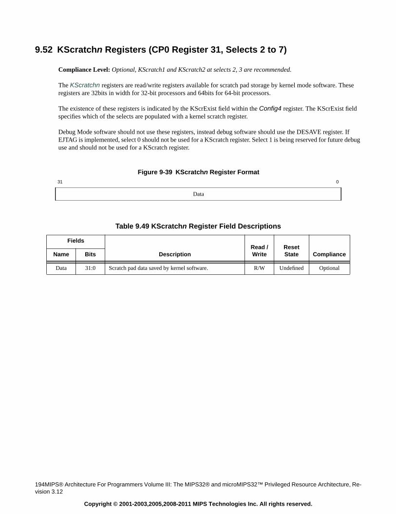
194MIPS® Architecture For Programmers Volume III: The MIPS32® and microMIPS32™ Privileged Resource Architecture, Re-vision 3.12
Copyright © 2001-2003,2005,2008-2011 MIPS Technologies Inc. All rights reserved.
9.52 KScratchn Registers (CP0 Register 31, Selects 2 to 7)
Compliance Level: Optional, KScratch1 and KScratch2 at selects 2, 3 are recommended.
The KScratchn registers are read/write registers available for scratch pad storage by kernel mode software. Theseregisters are 32bits in width for 32-bit processors and 64bits for 64-bit processors.
The existence of these registers is indicated by the KScrExist field within the Config4 register. The KScrExist fieldspecifies which of the selects are populated with a kernel scratch register.
Debug Mode software should not use these registers, instead debug software should use the DESAVE register. IfEJTAG is implemented, select 0 should not be used for a KScratch register. Select 1 is being reserved for future debuguse and should not be used for a KScratch register.
Figure 9-39 KScratchn Register Format31 0
Data
Table 9.49 KScratchn Register Field Descriptions
Fields
DescriptionRead /Write
ResetState ComplianceName Bits
Data 31:0 Scratch pad data saved by kernel software. R/W Undefined Optional
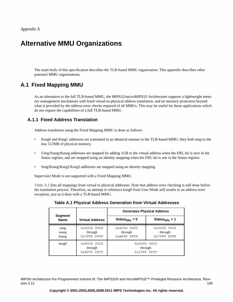
Appendix A
MIPS® Architecture For Programmers Volume III: The MIPS32® and microMIPS32™ Privileged Resource Architecture, Revi-sion 3.12 195
Copyright © 2001-2003,2005,2008-2011 MIPS Technologies Inc. All rights reserved.
Alternative MMU Organizations
The main body of this specification describes the TLB-based MMU organization. This appendix describes otherpotential MMU organizations.
A.1 Fixed Mapping MMU
As an alternative to the full TLB-based MMU, the MIPS32/microMIPS32 Architecture supports a lightweight mem-ory management mechanism with fixed virtual-to-physical address translation, and no memory protection beyondwhat is provided by the address error checks required of all MMUs. This may be useful for those applications whichdo not require the capabilities of a full TLB-based MMU.
A.1.1 Fixed Address Translation
Address translation using the Fixed Mapping MMU is done as follows:
• Kseg0 and Kseg1 addresses are translated in an identical manner to the TLB-based MMU: they both map to thelow 512MB of physical memory.
• Useg/Suseg/Kuseg addresses are mapped by adding 1GB to the virtual address when the ERL bit is zero in theStatus register, and are mapped using an identity mapping when the ERL bit is one in the Status register.
• Sseg/Ksseg/Kseg2/Kseg3 addresses are mapped using an identity mapping.
Supervisor Mode is not supported with a Fixed Mapping MMU.
Table A.1 lists all mappings from virtual to physical addresses. Note that address error checking is still done beforethe translation process. Therefore, an attempt to reference kseg0 from User Mode still results in an address errorexception, just as it does with a TLB-based MMU.
Table A.1 Physical Address Generation from Virtual Addresses
SegmentName Virtual Address
Generates Physical Address
StatusERL = 0 StatusERL = 1
usegsusegkuseg
0x0000 0000through
0x7FFF FFFF
0x4000 0000through
0xBFFF FFFF
0x0000 0000through
0x7FFF FFFF
kseg0 0x8000 0000through
0x9FFF FFFF
0x0000 0000through
0x1FFF FFFF
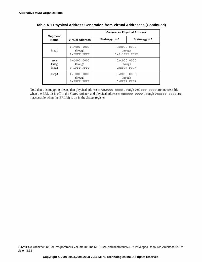
Alternative MMU Organizations
196MIPS® Architecture For Programmers Volume III: The MIPS32® and microMIPS32™ Privileged Resource Architecture, Re-vision 3.12
Copyright © 2001-2003,2005,2008-2011 MIPS Technologies Inc. All rights reserved.
Note that this mapping means that physical addresses 0x2000 0000 through 0x3FFF FFFF are inaccessiblewhen the ERL bit is off in the Status register, and physical addresses 0x8000 0000 through 0xBFFF FFFF areinaccessible when the ERL bit is on in the Status register.
kseg10xA000 0000
through0xBFFF FFFF
0x0000 0000through
0x0x1FFF FFFF
ssegkssegkseg2
0xC000 0000through
0xDFFF FFFF
0xC000 0000through
0xDFFF FFFF
kseg3 0xE000 0000through
0xFFFF FFFF
0xE000 0000through
0xFFFF FFFF
Table A.1 Physical Address Generation from Virtual Addresses (Continued)
SegmentName Virtual Address
Generates Physical Address
StatusERL = 0 StatusERL = 1
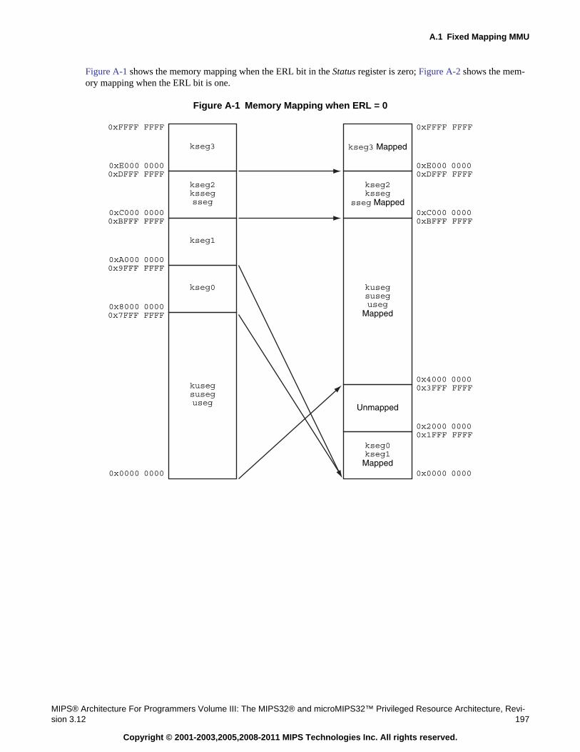
A.1 Fixed Mapping MMU
MIPS® Architecture For Programmers Volume III: The MIPS32® and microMIPS32™ Privileged Resource Architecture, Revi-sion 3.12 197
Copyright © 2001-2003,2005,2008-2011 MIPS Technologies Inc. All rights reserved.
Figure A-1 shows the memory mapping when the ERL bit in the Status register is zero; Figure A-2 shows the mem-ory mapping when the ERL bit is one.
Figure A-1 Memory Mapping when ERL = 0
0x0000 0000
0x7FFF FFFF0x8000 0000
0x9FFF FFFF0xA000 0000
0xBFFF FFFF0xC000 0000
0xDFFF FFFF0xE000 0000
0xFFFF FFFF
kseg0
kseg1
kseg3
kusegsuseguseg
kssegsseg
kseg2
0x0000 0000
0x1FFF FFFF0x2000 0000
0x3FFF FFFF0x4000 0000
0xBFFF FFFF0xC000 0000
0xDFFF FFFF0xE000 0000
0xFFFF FFFF
Unmapped
kseg3 Mapped
kssegsseg Mapped
kseg2
Mapped
kseg0kseg1
kusegsuseguseg
Mapped
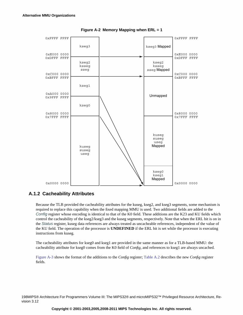
Alternative MMU Organizations
198MIPS® Architecture For Programmers Volume III: The MIPS32® and microMIPS32™ Privileged Resource Architecture, Re-vision 3.12
Copyright © 2001-2003,2005,2008-2011 MIPS Technologies Inc. All rights reserved.
Figure A-2 Memory Mapping when ERL = 1
A.1.2 Cacheability Attributes
Because the TLB provided the cacheability attributes for the kuseg, kseg2, and kseg3 segments, some mechanism isrequired to replace this capability when the fixed mapping MMU is used. Two additional fields are added to theConfig register whose encoding is identical to that of the K0 field. These additions are the K23 and KU fields whichcontrol the cacheability of the kseg2/kseg3 and the kuseg segments, respectively. Note that when the ERL bit is on inthe Status register, kuseg data references are always treated as uncacheable references, independent of the value ofthe KU field. The operation of the processor is UNDEFINED if the ERL bit is set while the processor is executinginstructions from kuseg.
The cacheability attributes for kseg0 and kseg1 are provided in the same manner as for a TLB-based MMU: thecacheability attribute for kseg0 comes from the K0 field of Config, and references to kseg1 are always uncached.
Figure A-3 shows the format of the additions to the Config register; Table A.2 describes the new Config registerfields.
0x0000 0000
0x7FFF FFFF0x8000 0000
0x9FFF FFFF0xA000 0000
0xBFFF FFFF0xC000 0000
0xDFFF FFFF0xE000 0000
0xFFFF FFFF
kseg0
kseg1
kseg3
kusegsuseguseg
kssegsseg
kseg2
0x0000 0000
0x7FFF FFFF0x8000 0000
0xBFFF FFFF0xC000 0000
0xDFFF FFFF0xE000 0000
0xFFFF FFFF
Unmapped
kseg3 Mapped
kssegsseg Mapped
kseg2
Mapped
kseg0kseg1
kusegsuseguseg
Mapped
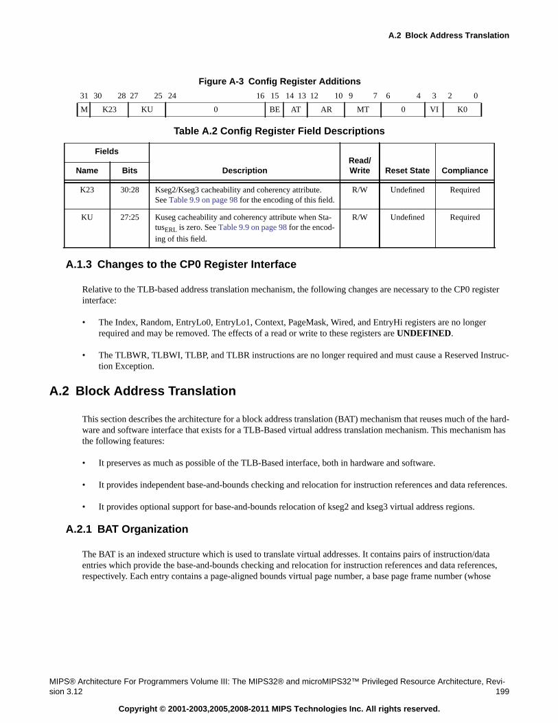
A.2 Block Address Translation
MIPS® Architecture For Programmers Volume III: The MIPS32® and microMIPS32™ Privileged Resource Architecture, Revi-sion 3.12 199
Copyright © 2001-2003,2005,2008-2011 MIPS Technologies Inc. All rights reserved.
A.1.3 Changes to the CP0 Register Interface
Relative to the TLB-based address translation mechanism, the following changes are necessary to the CP0 registerinterface:
• The Index, Random, EntryLo0, EntryLo1, Context, PageMask, Wired, and EntryHi registers are no longerrequired and may be removed. The effects of a read or write to these registers are UNDEFINED.
• The TLBWR, TLBWI, TLBP, and TLBR instructions are no longer required and must cause a Reserved Instruc-tion Exception.
A.2 Block Address Translation
This section describes the architecture for a block address translation (BAT) mechanism that reuses much of the hard-ware and software interface that exists for a TLB-Based virtual address translation mechanism. This mechanism hasthe following features:
• It preserves as much as possible of the TLB-Based interface, both in hardware and software.
• It provides independent base-and-bounds checking and relocation for instruction references and data references.
• It provides optional support for base-and-bounds relocation of kseg2 and kseg3 virtual address regions.
A.2.1 BAT Organization
The BAT is an indexed structure which is used to translate virtual addresses. It contains pairs of instruction/dataentries which provide the base-and-bounds checking and relocation for instruction references and data references,respectively. Each entry contains a page-aligned bounds virtual page number, a base page frame number (whose
Figure A-3 Config Register Additions
31 30 28 27 25 24 16 15 14 13 12 10 9 7 6 4 3 2 0
M K23 KU 0 BE AT AR MT 0 VI K0
Table A.2 Config Register Field Descriptions
Fields
DescriptionRead/Write Reset State ComplianceName Bits
K23 30:28 Kseg2/Kseg3 cacheability and coherency attribute.See Table 9.9 on page 98 for the encoding of this field.
R/W Undefined Required
KU 27:25 Kuseg cacheability and coherency attribute when Sta-tusERL is zero. See Table 9.9 on page 98 for the encod-
ing of this field.
R/W Undefined Required
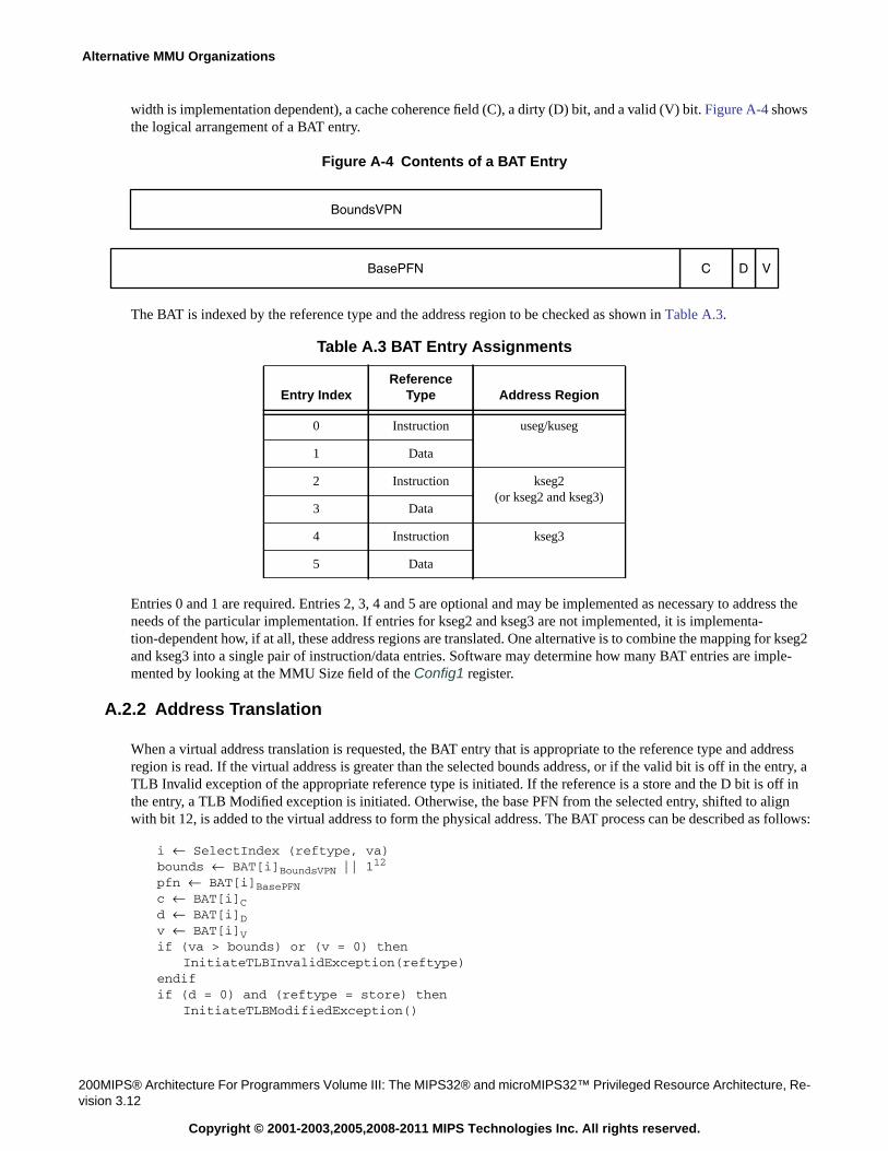
Alternative MMU Organizations
200MIPS® Architecture For Programmers Volume III: The MIPS32® and microMIPS32™ Privileged Resource Architecture, Re-vision 3.12
Copyright © 2001-2003,2005,2008-2011 MIPS Technologies Inc. All rights reserved.
width is implementation dependent), a cache coherence field (C), a dirty (D) bit, and a valid (V) bit. Figure A-4 showsthe logical arrangement of a BAT entry.
Figure A-4 Contents of a BAT Entry
The BAT is indexed by the reference type and the address region to be checked as shown in Table A.3.
Entries 0 and 1 are required. Entries 2, 3, 4 and 5 are optional and may be implemented as necessary to address theneeds of the particular implementation. If entries for kseg2 and kseg3 are not implemented, it is implementa-tion-dependent how, if at all, these address regions are translated. One alternative is to combine the mapping for kseg2and kseg3 into a single pair of instruction/data entries. Software may determine how many BAT entries are imple-mented by looking at the MMU Size field of the Config1 register.
A.2.2 Address Translation
When a virtual address translation is requested, the BAT entry that is appropriate to the reference type and addressregion is read. If the virtual address is greater than the selected bounds address, or if the valid bit is off in the entry, aTLB Invalid exception of the appropriate reference type is initiated. If the reference is a store and the D bit is off inthe entry, a TLB Modified exception is initiated. Otherwise, the base PFN from the selected entry, shifted to alignwith bit 12, is added to the virtual address to form the physical address. The BAT process can be described as follows:
i ← SelectIndex (reftype, va)bounds ← BAT[i]BoundsVPN || 112
pfn ← BAT[i]BasePFNc ← BAT[i]Cd ← BAT[i]Dv ← BAT[i]Vif (va > bounds) or (v = 0) then
InitiateTLBInvalidException(reftype)endifif (d = 0) and (reftype = store) then
InitiateTLBModifiedException()
Table A.3 BAT Entry Assignments
Entry IndexReference
Type Address Region
0 Instruction useg/kuseg
1 Data
2 Instruction kseg2(or kseg2 and kseg3)
3 Data
4 Instruction kseg3
5 Data
VDCBasePFN
BoundsVPN
A.2 Block Address Translation
MIPS® Architecture For Programmers Volume III: The MIPS32® and microMIPS32™ Privileged Resource Architecture, Revi-sion 3.12 201
Copyright © 2001-2003,2005,2008-2011 MIPS Technologies Inc. All rights reserved.
endifpa ← va + (pfn || 012)
Making all addresses out-of-bounds can only be done by clearing the valid bit in the BAT entry. Setting the boundsvalue to zero leaves the first virtual page mapped.
A.2.3 Changes to the CP0 Register Interface
Relative to the TLB-based address translation mechanism, the following changes are necessary to the CP0 registerinterface:
• The Index register is used to index the BAT entry to be read or written by the TLBWI and TLBR instructions.
• The EntryHi register is the interface to the BoundsVPN field in the BAT entry.
• The EntryLo0 register is the interface to the BasePFN and C, D, and V fields of the BAT entry. The register hasthe same format as for a TLB-based MMU.
• The Random, EntryLo1, Context, PageMask, and Wired registers are eliminated. The effects of a read orwrite to these registers is UNDEFINED.
• The TLBP and TLBWR instructions are unnecessary. The TLBWI and TLBR instructions reference the BATentry whose index is contained in the Index register. The effects of executing a TLBP or TLBWR are UNDE-FINED, but processors should signal a Reserved Instruction Exception.
Alternative MMU Organizations
202MIPS® Architecture For Programmers Volume III: The MIPS32® and microMIPS32™ Privileged Resource Architecture, Re-vision 3.12
Copyright © 2001-2003,2005,2008-2011 MIPS Technologies Inc. All rights reserved.
A.3 Dual Variable-Page-Size and Fixed-Page-Size TLBs
Most MIPS CPU cores implement a fully associative Joint TLB. Unfortunately, such fully-associative structures canbe slow, can require a large amount of logic components to implement and can dissipate a lot of power. The numberof entries for a fully associative array that can be practically implemented is not large.
In high performance systems, it is desirable to minimize the frequency of TLB misses. In small and low-cost systems,it is desirable to keep the implementation costs of a TLB to a minimum. This section describes an optional alternativeMMU configuration which decreases the implementation costs of a small TLB as well as allows for a TLB that canmap a very large number of pages to be reasonably implemented.
A.3.1 MMU Organization
This alternative MMU configuration uses two TLB structures.
1. This first TLB is called the Fixed-Page-Size TLB or the FTLB.
• At any one time, all entries within the FTLB use a shared, common page size.
• The FTLB is not fully-associative, but rather set associative.
• The number of ways per set is implementation specific.
• The number of sets is implementation specific.
• The common page size is also implementation specific.
• The common page size is allowed to be software configurable. The choice of the common page size is doneonce for the entire FTLB, not on a per-entry basis. This configuration by software can only be done after afull flush/initialization of the FTLB, before there are any valid entries within the FTLB. Implementations arealso allowed to support only one page size for the FTLB - in that case, the FTLB page size is fixed by hard-ware and not software configurable.
2. The second TLB is called the Variable-Page-Size TLB or the VTLB.
• The choice of page size is done on a per-entry basis. That is, one VTLB entry can use a pagesize that is dif-ferent from the size used by another VTLB entry.
• The VTLB is fully-associative.
• The number of entries is implementation specific.
• The set of allowable page sizes for VTLB entries is implementation specific.
Just as for the JTLB, both the FTLB and VTLB are shared between the instruction stream and the data stream. Foraddress translation, the virtual address is presented to both the FTLB and VTLB in parallel. Entries in both structuresare accessed in parallel to search for the physical address.
The use of two TLB structures has these benefits:
• The implementation costs of building a set-associative TLB with many entries can be much less than that ofimplementing a large fully-associative TLB.
A.3 Dual Variable-Page-Size and Fixed-Page-Size TLBs
MIPS® Architecture For Programmers Volume III: The MIPS32® and microMIPS32™ Privileged Resource Architecture, Revi-sion 3.12 203
Copyright © 2001-2003,2005,2008-2011 MIPS Technologies Inc. All rights reserved.
• The existence of a VTLB retains the capability of using large pages to map large sections of physical memorywithout consuming a large number of entries in the FTLB.
Random replacement of pages in the MMU happens mainly in the FTLB. In most operating systems, on-demand pag-ing only uses one page size so the FTLB is sufficient for this purpose. Some of the address bits of the specified virtualaddress are used to index into the FTLB as appropriate for the chosen FTLB array size. The method of choosingwhich FTLB way to modify is implementation specific.
The VTLB is very similiar to the JTLB. The C0_PageMask register is used to program the page size used for a par-ticular VTLB entry.
The configuration of the FTLB is reflected in the FTLB fields within the new C0_Config4 register. The size of theVTLB is reflected in the C0_Config1MMUSize-1 field. The presense of the dual FTLB and VTLB is denoted by thevalue of 0x4 in C0_ConfigMT register field. These registers are described in “Changes to the COP0 Registers” onpage 206.
Most implementations would choose to build a VTLB with a smaller number of entries and a FTLB with a largernumber of entries. This combination allows for many on-demand fixed-sized pages as well as for a small number oflarge address blocks to be simultaneously mapped by the MMU.
A.3.2 Programming Interface
The software programming interface used for the fully-associative JTLB is maintained as much as possible todecrease the amount of software porting.
Also for that purpose, each entry in the FTLB as well as the VTLB use one tag (VPN2) to map two physical pages(PFN), just as in the JTLB. The entries in either array are accessed through the C0_EntryHi and C0_EntryLo0/1registers.
Entries in either array (FTLB or VTLB) can be accessed with the TLBWI and TLBWR instructions.
The PageMask register is used to set the page size for the VTLB entries. This register is also used to choose whicharray (FTLB or VTLB) to write for the TLBWR instruction.
For the rest of this section, the following parameters are used:
3. FPageSize - the page size used by the FTLB entries
4. FSetSize - Number of entries in one way of the FTLB.
5. FWays - Number of ways within a set of the FTLB.
6. VIndex - Number of entries in the VTLB.
For the C0_Index , the C0_Wired registers, the TLBP, TLBR and TLBWI instructions; the VTLB occupies indices0 to VIndex-1. The FTLB occupies indices VIndex to VIndex + (FSetSize * FWays)-1.
The TLBP instruction produces a value which can be used by the TLBWI instruction without modification by soft-ware. When referring to the FTLB, the value is the concatentation of the selected FTLB way and set, and incrementedby the size of the VTLB. For example, {selected FTLB Way, selected FTLB Set} + VIndex.
Alternative MMU Organizations
204MIPS® Architecture For Programmers Volume III: The MIPS32® and microMIPS32™ Privileged Resource Architecture, Re-vision 3.12
Copyright © 2001-2003,2005,2008-2011 MIPS Technologies Inc. All rights reserved.
If C0_PageMask is set to the page size used by the FTLB, the TLBWR instruction modifies entries within theFTLB.
How the FTLB set-associative array is indexed is implementation specific. In any indexing scheme, the least signifi-cant address bit that can be used for indexing is log2(FPageSize)+1. The number of index bits needed to select thecorrect set within the FTLB array is log2(FSetSize).
Since the FTLB array can be modified through the TLBWI instruction, it is possible for software to choose an inap-propriate FTLB index value for the specified virtual address. In this case, it is implementation specific whether aMachine Check exception is generated for the TLBWI instruction.
The method of choosing which FTLB way to modify is implementation specific.
If C0_PageMask is not set to the pagesize used by the FTLB, the TLBWR instruction modifies entries within theVTLB. The VTLB entry to be written is specified by the log2(VIndex) least significant bits of the C0_Random reg-ister value.
For both the TLBWR and TLBWI instruction, it is implementation specific whether both (FTLB and VTLB) arraysare checked for duplicate or overlapping entries and whether a Machine Check exception is generated for these cases.
A.3.2.1 Example with chosen FTLB and VTLB sizes
As an example, let’s assume an implementation chooses these values:
1. FPageSize - 4KB used by the FTLB entries
2. FSetSize - 128 in one way of the FTLB.
3. FWays - 4 ways within a set of the FTLB. (The FTLB has (128 sets x 4 ways/set) 512 entries, capable of map-ping (512 entries x 2 pages/entry x 4KB/page) 4MB of address space simultaneously.
4. VIndex - 8 entries in the VTLB.
For the C0_Index, the C0_Wired registers, the TLBP, TLBR and TLBWI instructions; the VTLB occupies indices 0to 7. The FTLB occupies indices 8 to 519.
The FTLB entries have a VPN2 field which starts at virtual address bit 12.
The least significant virtual address bit that can be used for FTLB indexing is virtual address 13. To index the FTLBset-associative array, 7 index bits are needed.
In this simple example, the design uses contiguous virtual address bits directly for indexing the FTLB ( it does notcreate a hash for the FTLB indexing). The FTLB set-associative array is indexed using virtual address bits 19:13. TheTLBWR instruction uses these address bits held in C0_EntryHi.
In this simple example, the design uses a cycle counter of 2 bits for way selection within the FTLB.
The Random register field within C0_Random is 3 bits wide to select the entry within the VTLB.
A.3 Dual Variable-Page-Size and Fixed-Page-Size TLBs
MIPS® Architecture For Programmers Volume III: The MIPS32® and microMIPS32™ Privileged Resource Architecture, Revi-sion 3.12 205
Copyright © 2001-2003,2005,2008-2011 MIPS Technologies Inc. All rights reserved.
A.3.3 Changes to the TLB Instructions
TLBP
Both the VTLB and the FTLB are probed in parallel for the specified virtual address.
If the address hits in the VTLB, C0_Index specifies the entry within the VTLB [ a value within 0 to VIndex-1].
If the address hits in the FTLB, C0_Index specifies the entry within the FTLB [ a value within VIndex to VIn-dex+(FSetSize * FWays)-1 ]. Which bits are used to encode the selected FTLB set as opposed to which bits areused to encode the selected FTLB way is implementation specific, but must match what is expected by theTLBWI instruction implementation. C0_PageMask reflects the pagesize used by the FTLB.
TLBR
Either a VTLB entry or a FTLB entry is read depending on the specified index in C0_Index.
Index values of 0 to VIndex-1 access the VTLB. Index values VIndex to VIndex+(FSetSize * FWays)-1 accessthe FTLB.
TLBWI
Either the VTLB or FTLB entry is written depending on the specified index in C0_Index.
Index values of 0 to VIndex-1 access the VTLB. Index values VIndex to VIndex+(FSetSize * FWays)-1 accessthe FTLB.
It is implementation specific if the hardware checks the VPN2 field of C0_EntryHi is appropriate for the speci-fied set within the FTLB. The implementation may generate a machine-check exception if the VPN2 field is notappropriate for the specified set.
It is implementation specific if the hardware checks both arrays (FTLB and VTLB) for valid duplicate or over-lapping entries and if the hardware signals a Machine Check exception for these cases.
TLBWR
Either the VTLB or FTLB entry is written depending on the specified pagesize in C0_PageMask.
If C0_PageMask is set to any pagesize other than that used by the FTLB, the TLBWR instruction modifies aVTLB entry. The VTLB entry is specified by the Random register field within C0_Random.
If C0_PageMask is set to the pagesize used by the FTLB, the TLBWR modifies a FTLB entry. The FTLBset-associative array is indexed in an implementation-specific manner.
The method of selecting which FTLB way to modify is implementation specific.
It is implementation specific if the hardware checks both arrays (FTLB and VTLB) for valid duplicate or over-lapping entries and if the hardware signals a Machine Check exception for these cases.
Alternative MMU Organizations
206MIPS® Architecture For Programmers Volume III: The MIPS32® and microMIPS32™ Privileged Resource Architecture, Re-vision 3.12
Copyright © 2001-2003,2005,2008-2011 MIPS Technologies Inc. All rights reserved.
A.3.4 Changes to the COP0 Registers
C0_Config4 (CP0 Register 16, Select 4)
A new register introduced to reflect the FTLB configuration. Config4MMUExtDef register field must be set to avalue of 2 to reflect that the Dual VTLB and FTLB configuration is implemented. If either Config4 is not imple-mented or the Config4MMUExtDef field is not fixed to 2, the Dual VTLB/FTLB configuration is not implemented.
If Config4MMUExtDef is fixed to a value of 2, the FTLBPageSize, FTLBWays and FTLBSets fields reflect theFTLB configuration. Please refer to “Configuration Register 4 (CP0 Register 16, Select 4)” on page 165 for moredetail on this register.
C0_Config1 (CP0 Register 16, Select 1)
If Config4MMUExtDef is fixed to a value of 2, the MMUSize-1 register field is redefined to reflect only the size ofthe VTLB.
C0_Config (CP0 Register 16, Select 0)
If Config4MT is fixed to a value of 4, the implemented MMU Type is the dual FTLB and VTLB configuration.
C0_Index (CP0 Register 0, Select 0)
If Config4MMUExtDef is fixed to a value of 2, the register is redefined in this way:
The value held in the Index field can refer to either an entry in the FTLB or the VTLB. Index values of 0 toVIndex-1 access the VTLB. Index values VIndex to VIndex+(FSetSize * FWays)-1 access the FTLB. Whichbits in the register field which encode the FTLB set as opposed to which bits encode the FTLB way is imple-mentation specific, but must match what is expected by the TLBWI instruction implementation.
C0_Random (CP0 Register 1, Select 0)
If Config4MMUExtDef is fixed to a value of 2, the register is redefined in this way:
If the value in C0_PageMask is not set to the page-size used by the FTLB, and a TLBWR instruction isexecuted, a VTLB entry is modified. The Random register field is used to select the VTLB entry which ismodified.
If the value in C0_PageMask is set to the page-size used by the FTLB, and a TLBWR instruction is exe-cuted, a FTLB entry is modified. It is implementation specific whether the C0_RANDOM register is used toselect the FTLB entry.
The upper bound of the Random register field value is VIndex.
C0_Wired (CP0 Register 6, Select 0)
If Config4MMUExtDef is fixed to a value of 2, the Wired register field can only hold a value of VIndex-1 or less.That is, only VTLB entries can be wired down.
A.3 Dual Variable-Page-Size and Fixed-Page-Size TLBs
MIPS® Architecture For Programmers Volume III: The MIPS32® and microMIPS32™ Privileged Resource Architecture, Revi-sion 3.12 207
Copyright © 2001-2003,2005,2008-2011 MIPS Technologies Inc. All rights reserved.
C0_PageMask (CP0 Register 5, Select 0)
If Config4MMUExtDef is fixed to a value of 2, the register is redefined in this way:
The Mask and MaskX field values determine whether the VTLB or the FTLB is modified by a TLBWRinstruction.
The Mask and MaskX register fields do not affect the TLB address match operation for FTLB entries. Thepagesize used by the FTLB entries are specified by the Config4FPageSize register field.
The software writeable bits in the Mask and MaskX fields reflect what page sizes are available in the VTLB.These fields do not reflect the page sizes which are available in the FTLB.
Alternative MMU Organizations
208MIPS® Architecture For Programmers Volume III: The MIPS32® and microMIPS32™ Privileged Resource Architecture, Re-vision 3.12
Copyright © 2001-2003,2005,2008-2011 MIPS Technologies Inc. All rights reserved.
A.3.5 Software Compatibility
One of the main software visible changes introducted by this alternative MMU are the values reported in theC0_Index register. Previously, it was just a simple linear index. For this alternative MMU configuration, the valuereflects both a selected way as well as a selected set when a FTLB entry is specified.
Fortunately, this Index value isn’t frequently generated by software nor read by software. Instead, the contents of theC0_Index register is generated by hardware upon a TLBP instruction. Software then just issues the TLBWI instruc-tion once the C0_EnLo* registers have been appropriately modified.
Another software visible change is that the MMUSize-1 field no longer reports the entire MMU size. For TLB initial-ization and TLB flushing, the contents of Config1MMUSize-1, Config4FTLBWays and Config4FTLBSets register fieldsmust all be read to calculate the entire number of TLB entries that must be initialized. TLB initialization and flushingare the only times software needs to generate an Index value to write into the C0_Index register.
Only the VTLB entries may be wired down. This limitation is due to using some of the EntryHi VPN2 bits to indexthe FTLB array.
If a page using the FTLB page-size is to be wired down, that page must be programmed into the VTLB using theTLBWI instruction, as the TLBWR instruction would only access the FTLB in that situation and could not access anywired-down TLB entry. The TLBWI instruction is normally used for wired-down pages, so this restriction should notaffect existing software.
Appendix B
MIPS® Architecture For Programmers Volume III: The MIPS32® and microMIPS32™ Privileged Resource Architecture, Revi-sion 3.12 209
Copyright © 2001-2003,2005,2008-2011 MIPS Technologies Inc. All rights reserved.
Revision History
In the left hand page margins of this document you may find vertical change bars to note the location of significantchanges to this document since its last release. Significant changes are defined as those which you should take note ofas you use the MIPS IP. Changes to correct grammar, spelling errors or similar may or may not be noted with changebars. Change bars will be removed for changes which are more than one revision old.
Please note: Limitations on the authoring tools make it difficult to place change bars on changes to figures. Changebars on figure titles are used to denote a potential change in the figure itself.
Revision Date Description
0.92 January 20, 2001 Internal review copy of reorganized and updated architecture documentation.
0.95 March 12, 2001 Clean up document for external review release
1.00 August 29, 2002 Update based on review feedback:• Change ProbEn to ProbeTrap in the EJTAG Debug entry vector location dis-
cussion.• Add cache error and EJTAG Debug exceptions to the list of exceptions that
do not go through the general exception processing mechanism.• Fix incorrect branch offset adjustment in general exception processing
pseudo code to deal with extended MIPS16e instructions.• Add ConfigVI to denote an instruction cache with both virtual indexing and
virtual tags.• Correct XContext register description to note that both BadVPN2 and R
fields are UNPREDICTABLE after an address error exception.• Note that Supervisor Mode is not supported with a Fixed Mapping MMU.• Define TagLo bits 4..3 as implementation dependent.• Describe the intended usage model differences between Reset and Soft Reset
Exceptions.• Correct the minimum number of TLB entries to be 3, not 2, and show an
example of the need for 3.• Modify the description of PageMask and the TLB lookup process to
acknowledge the fact that not all implementations may support all page sizes.
1.90 September 1, 2002 Update the specification with the changes introduced in Release 2 of the Archi-tecture. Changes in this revision include:• The following new Coprocessor 0 registers were added: EBase, HWREna,
IntCtl, PageGrain, SRSCtl, SRSMap.• The following Coprocessor 0 registers were modified: Cause, Config,
Config2, Config3, EntryHi, EntryLo0, EntryLo1, PageMask, PerfCnt, Status,WatchHi, WatchLo.
• The descriptions of Virtual memory, exceptions, and hazards have beenupdated to reflect the changes in Release 2.
• A chapter on GPR shadow regsiters has been added.• The chapter on CP0 hazards has been completely rewriten to reflect the
Release 2 changes.
Revision History
210MIPS® Architecture For Programmers Volume III: The MIPS32® and microMIPS32™ Privileged Resource Architecture, Re-vision 3.12
Copyright © 2001-2003,2005,2008-2011 MIPS Technologies Inc. All rights reserved.
2.00 June 9, 2003 Complete the update to include Release 2 changes. These include:• Make bits 12..11 of the PageMask register power up zero and be gated by 1K
page enable. This eliminates the problem of having these bits set to 0b11 on aRelease 2 chip in which kernel software has not enabled 1K page support.
• Correct the address of the cache error vector when the BEV bit is 1. It shouldbe 0xBFC0.0300,. not 0xBFC0.0200.
• Correct the introduction to shadow registers to note that the SRSCtl registeris not updated at the end of an exception in which StatusBEV = 1.
• Clarify that a MIPS16e PC-relative load reference is a data reference for thepurposes of the Watch registers.
• Add note about a hardware interrupt being deasserted between the time thatthe processor detects the interrupt request and the time that the softwareinterrupt handler runs. Software must be prepared for this case and simplydismiss the interrupt via an ERET.
• Add restriction that software must set EBase15..12 to zero in all bit positions
less than or equal to the most significant bit in the vector offset. This is onlyrequired in certain combinations of vector number and vector spacing whenusing VI or EIC Interrupt modes.
• Add suggested software TLB init routine which reduced the probability oftriggering a machine check.
2.50 July 1, 2005 Changes in this revision:• Correct the encoding table description for the CausePCI bit to indicate that the
bit controlls the performance counter, not the timer interrupt.• Correct the figure Interrupt Generation for External Interrupt Controller
Interrupt Mode to show CauseIP1..0 going to the EIC, rather than StatusIP1..0
• Update all files to FrameMaker 7.1.• Update reset exception list to reflect missing Release 2 reset requirements.• Define bits 31..30 in the HWREna register as access enables for the imple-
mentation-dependent hardware registers 31 and 30.• Add definition for Coprocessor 0 Enable to Operating Modes chapter.• Add K23 and KU fields to main Config register definition as a pointer to the
Fixed Mapping MMU appendix.• Add specific note about the need to implement all shadow sets between 0 and
HSS - no holes are allowed.• Change the hazard from a software write to the SRSCtlPSS field and a
RDPGPR and WRPGPR and instruction hazard vs. an execution hazard.• Correct the pseudo-code in the cache error exception description to reflect the
Release 2 change that introduced EBase.• Document that EHB clears instruction state change hazards for writes to
interrupt-related fields in the Status, Cause, Compare, and PerfCnt regis-ters.
• Note that implementation-dependent bits in the Status and Config registersshould be defined in such a way that standard boot software will run, and thatsoftware which preserves the value of the field when writing the registers willalso run correctly.
• With Release 2 of the Architecture the FR bit in the Status register should bea R/W bit, not a R bit.
• Improve the organization of the CP0 hazards table, and document thatDERET, ERET, and exceptions and interrupts clear all hazards before theinstruction fetch at the target instruction.
• Add list of MIPS® MT CP0 registers and MIPS MT and MIPS® DSPpresent bits in the Config3 register.
Revision Date Description
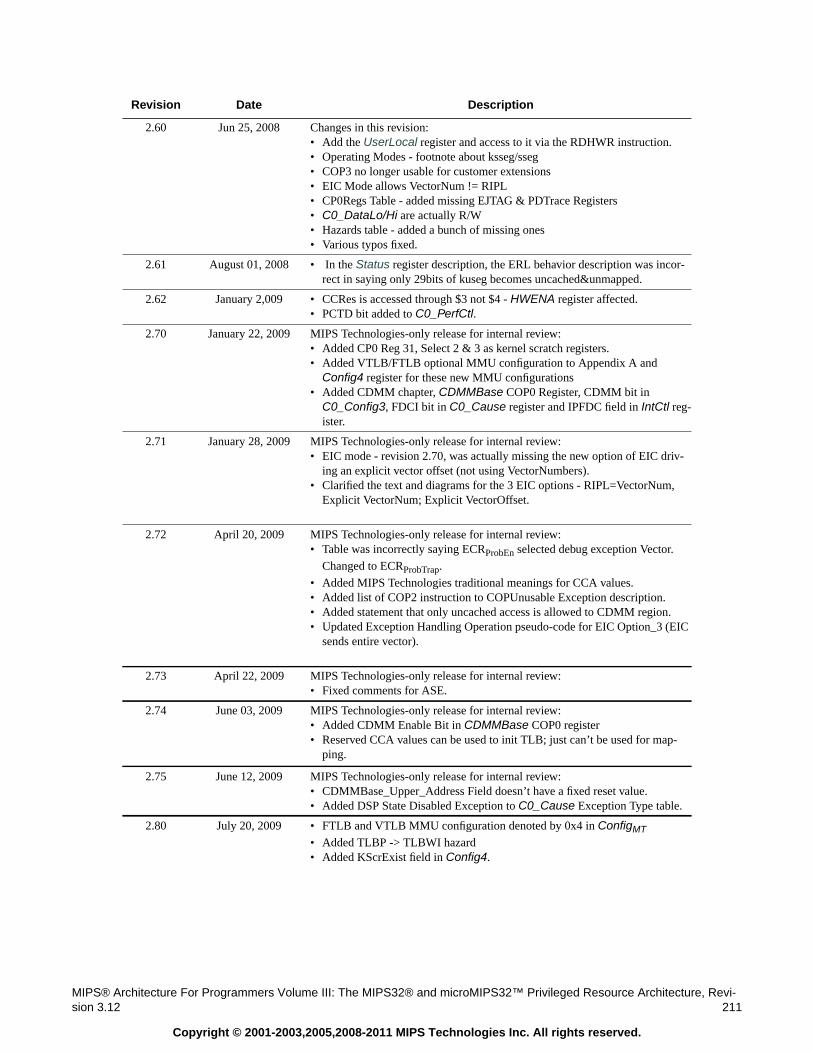
MIPS® Architecture For Programmers Volume III: The MIPS32® and microMIPS32™ Privileged Resource Architecture, Revi-sion 3.12 211
Copyright © 2001-2003,2005,2008-2011 MIPS Technologies Inc. All rights reserved.
2.60 Jun 25, 2008 Changes in this revision:• Add the UserLocal register and access to it via the RDHWR instruction.• Operating Modes - footnote about ksseg/sseg• COP3 no longer usable for customer extensions• EIC Mode allows VectorNum != RIPL• CP0Regs Table - added missing EJTAG & PDTrace Registers• C0_DataLo/Hi are actually R/W• Hazards table - added a bunch of missing ones• Various typos fixed.
2.61 August 01, 2008 • In the Status register description, the ERL behavior description was incor-rect in saying only 29bits of kuseg becomes uncached&unmapped.
2.62 January 2,009 • CCRes is accessed through $3 not $4 - HWENA register affected.• PCTD bit added to C0_PerfCtl.
2.70 January 22, 2009 MIPS Technologies-only release for internal review:• Added CP0 Reg 31, Select 2 & 3 as kernel scratch registers.• Added VTLB/FTLB optional MMU configuration to Appendix A and
Config4 register for these new MMU configurations• Added CDMM chapter, CDMMBase COP0 Register, CDMM bit in
C0_Config3, FDCI bit in C0_Cause register and IPFDC field in IntCtl reg-ister.
2.71 January 28, 2009 MIPS Technologies-only release for internal review:• EIC mode - revision 2.70, was actually missing the new option of EIC driv-
ing an explicit vector offset (not using VectorNumbers).• Clarified the text and diagrams for the 3 EIC options - RIPL=VectorNum,
Explicit VectorNum; Explicit VectorOffset.
2.72 April 20, 2009 MIPS Technologies-only release for internal review:• Table was incorrectly saying ECRProbEn selected debug exception Vector.
Changed to ECRProbTrap.
• Added MIPS Technologies traditional meanings for CCA values.• Added list of COP2 instruction to COPUnusable Exception description.• Added statement that only uncached access is allowed to CDMM region.• Updated Exception Handling Operation pseudo-code for EIC Option_3 (EIC
sends entire vector).
2.73 April 22, 2009 MIPS Technologies-only release for internal review:• Fixed comments for ASE.
2.74 June 03, 2009 MIPS Technologies-only release for internal review:• Added CDMM Enable Bit in CDMMBase COP0 register• Reserved CCA values can be used to init TLB; just can’t be used for map-
ping.
2.75 June 12, 2009 MIPS Technologies-only release for internal review:• CDMMBase_Upper_Address Field doesn’t have a fixed reset value.• Added DSP State Disabled Exception to C0_Cause Exception Type table.
2.80 July 20, 2009 • FTLB and VTLB MMU configuration denoted by 0x4 in ConfigMT• Added TLBP -> TLBWI hazard• Added KScrExist field in Config4.
Revision Date Description
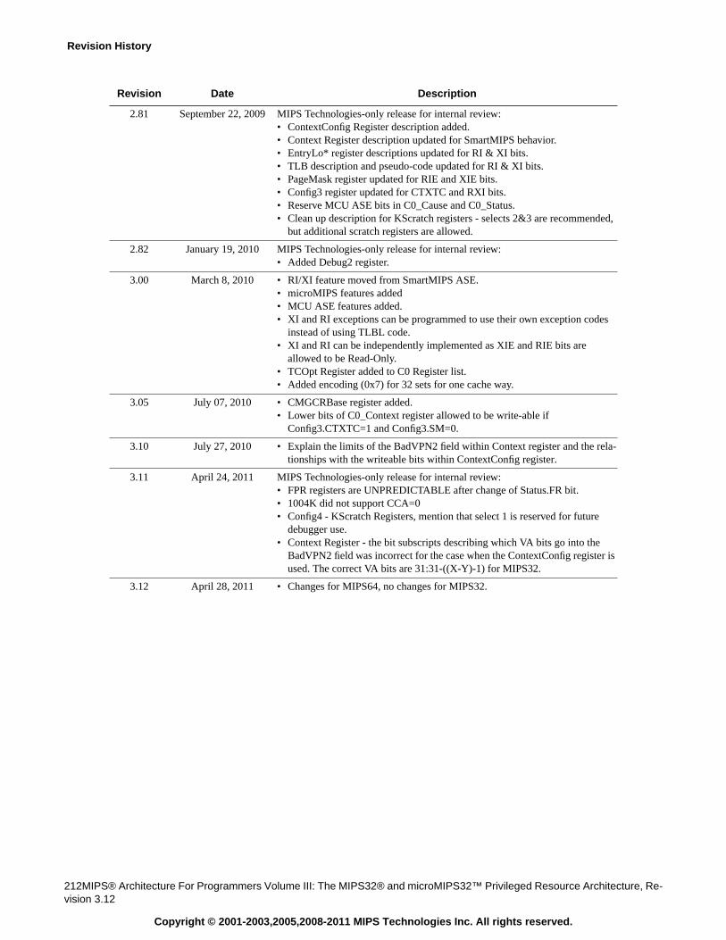
Revision History
212MIPS® Architecture For Programmers Volume III: The MIPS32® and microMIPS32™ Privileged Resource Architecture, Re-vision 3.12
Copyright © 2001-2003,2005,2008-2011 MIPS Technologies Inc. All rights reserved.
2.81 September 22, 2009 MIPS Technologies-only release for internal review:• ContextConfig Register description added.• Context Register description updated for SmartMIPS behavior.• EntryLo* register descriptions updated for RI & XI bits.• TLB description and pseudo-code updated for RI & XI bits.• PageMask register updated for RIE and XIE bits.• Config3 register updated for CTXTC and RXI bits.• Reserve MCU ASE bits in C0_Cause and C0_Status.• Clean up description for KScratch registers - selects 2&3 are recommended,
but additional scratch registers are allowed.
2.82 January 19, 2010 MIPS Technologies-only release for internal review:• Added Debug2 register.
3.00 March 8, 2010 • RI/XI feature moved from SmartMIPS ASE.• microMIPS features added• MCU ASE features added.• XI and RI exceptions can be programmed to use their own exception codes
instead of using TLBL code.• XI and RI can be independently implemented as XIE and RIE bits are
allowed to be Read-Only.• TCOpt Register added to C0 Register list.• Added encoding (0x7) for 32 sets for one cache way.
3.05 July 07, 2010 • CMGCRBase register added.• Lower bits of C0_Context register allowed to be write-able if
Config3.CTXTC=1 and Config3.SM=0.
3.10 July 27, 2010 • Explain the limits of the BadVPN2 field within Context register and the rela-tionships with the writeable bits within ContextConfig register.
3.11 April 24, 2011 MIPS Technologies-only release for internal review:• FPR registers are UNPREDICTABLE after change of Status.FR bit.• 1004K did not support CCA=0• Config4 - KScratch Registers, mention that select 1 is reserved for future
debugger use.• Context Register - the bit subscripts describing which VA bits go into the
BadVPN2 field was incorrect for the case when the ContextConfig register isused. The correct VA bits are 31:31-((X-Y)-1) for MIPS32.
3.12 April 28, 2011 • Changes for MIPS64, no changes for MIPS32.
Revision Date Description