Embed Size (px)
Citation preview

MCP73831/2Miniature Single-Cell, Fully Integrated Li-Ion,Li-Polymer Charge Management Controllers
Features
• Linear Charge Management Controller:
- Integrated Pass Transistor
- Integrated Current Sense
- Reverse Discharge Protection
• High Accuracy Preset Voltage Regulation: + 0.75%
• Four Voltage Regulation Options:
- 4.20V, 4.35V, 4.40V, 4.50V
• Programmable Charge Current: 15 mA to 500 mA
• Selectable Preconditioning:
- 10%, 20%, 40%, or Disable
• Selectable End-of-Charge Control:
- 5%, 7.5%, 10%, or 20%
• Charge Status Output
- Tri-State Output - MCP73831
- Open-Drain Output - MCP73832
• Automatic Power-Down
• Thermal Regulation
• Temperature Range: -40°C to +85°C
• Packaging:
- 8-Lead, 2 mm x 3 mm DFN
- 5-Lead, SOT-23
Applications
• Lithium-Ion/Lithium-Polymer Battery Chargers
• Personal Data Assistants
• Cellular Telephones
• Digital Cameras
• MP3 Players
• Bluetooth Headsets
• USB Chargers
Typical Application
Description:
The MCP73831/2 devices are highly advanced linearcharge management controllers for use in space-limited, cost-sensitive applications. The MCP73831/2are available in an 8-Lead, 2 mm x 3 mm DFN packageor a 5-Lead, SOT-23 package. Along with their smallphysical size, the low number of external componentsrequired make the MCP73831/2 ideally suited forportable applications. For applications charging from aUSB port, the MCP73831/2 adhere to all thespecifications governing the USB power bus.
The MCP73831/2 employ a constant-current/constant-voltage charge algorithm with selectablepreconditioning and charge termination. The constantvoltage regulation is fixed with four available options:4.20V, 4.35V, 4.40V or 4.50V, to accommodate new,emerging battery charging requirements. The constantcurrent value is set with one external resistor. TheMCP73831/2 devices limit the charge current based ondie temperature during high power or high ambientconditions. This thermal regulation optimizes thecharge cycle time while maintaining device reliability.
Several options are available for the preconditioningthreshold, preconditioning current value, chargetermination value and automatic recharge threshold.The preconditioning value and charge terminationvalue are set as a ratio or percentage of theprogrammed constant current value. Preconditioningcan be disabled. Refer to Section 1.0 “ElectricalCharacteristics” for available options and theProduct Identification System for standard options.
The MCP73831/2 devices are fully specified over theambient temperature range of -40°C to +85°C.
Package Types
STAT
VDD
VSS
PROG
VBAT +
-
SingleLi-IonCell
4
MCP73831
5
3
1
500 mA Li-Ion Battery Charger
2
VIN
4.7 μF
470Ω 2 kΩ
4.7 μFVBAT
VSS
VDD
1
2
3
5
4
PROGSTAT
MCP73831/22×3 DFN*
VBAT
VDD
VBAT
NC
VSS
1
2
3
4
8
7
6
5 STAT
PROGVDD
* Includes Exposed Thermal Pad (EP); see Table 3-1.
EP9
MCP73831/2SOT-23-5
2005-2013 Microchip Technology Inc. DS20001984F-page 1

MCP73831/2
Functional Block Diagram
+
-
REFERENCEGENERATOR
VREF(1.22V)
VBAT
VDD
STAT
PROG
VBAT
G=0.001
VSS
DIRECTION CONTROL
477 kΩ
255 kΩ
UVLO
+
-
+
-
SHDN
DIRECTION CONTROL
0.5 µA
PRECONDITION
6 µA
6 µA
+
-
TERMINATION
+
-
43.6 kΩ
+
-
CA
3.9 kΩ
111 kΩ
190 kΩ
7 kΩ
15 kΩ
182.3 kΩ111 kΩ
CHARGE
+
-
+
-
VA
89 kΩ
361 kΩ
100 kΩ
0.5 µA
VDD
MCP73831 ONLY
DS20001984F-page 2 2005-2013 Microchip Technology Inc.

MCP73831/2
1.0 ELECTRICAL CHARACTERISTICS
Absolute Maximum Ratings†
VDD...................................................................................7.0V
All Inputs and Outputs w.r.t. VSS ............... -0.3 to (VDD+0.3)V
Maximum Junction Temperature, TJ ............ Internally Limited
Storage temperature .....................................-65°C to +150°C
ESD protection on all pins:
Human Body Model (1.5 kΩ in Series with 100 pF) .......≥ 4 kV
Machine Model (200 pF, No Series Resistance) .............400V
† Notice: Stresses above those listed under “MaximumRatings” may cause permanent damage to the device.This is a stress rating only and functional operation ofthe device at those or any other conditions above thoseindicated in the operational listings of this specificationis not implied. Exposure to maximum rating conditionsfor extended periods may affect device reliability.
DC CHARACTERISTICSElectrical Specifications: Unless otherwise indicated, all limits apply for VDD= [VREG(typical) + 0.3V] to 6V, TA = -40°C to +85°C. Typical values are at +25°C, VDD = [VREG (typical) + 1.0V]
Parameters Sym. Min. Typ. Max. Units Conditions
Supply Input
Supply Voltage VDD 3.75 — 6 V
Supply Current ISS — 510 1500 µA Charging
— 53 200 µA Charge Complete,No Battery
— 25 50 µA PROG Floating
— 1 5 µA VDD < (VBAT - 50 mV)
— 0.1 2 µA VDD < VSTOP
UVLO Start Threshold VSTART 3.3 3.45 3.6 V VDD Low-to-High
UVLO Stop Threshold VSTOP 3.2 3.38 3.5 V VDD High-to-Low
UVLO Hysteresis VHYS — 70 — mV
Voltage Regulation (Constant-Voltage Mode)
Regulated Output Voltage VREG 4.168 4.20 4.232 V PIC18FXXXX-2
4.317 4.35 4.383 V PIC18FXXXX-3
4.367 4.40 4.433 V PIC18FXXXX-4
4.466 4.50 4.534 V PIC18FXXXX-5
VDD = [VREG(typical)+1V]IOUT = 10 mA TA = -5°C to +55°C
Line Regulation |(ΔVBAT/VBAT)/ΔVDD|
— 0.09 0.30 %/V VDD = [VREG(typical)+1V] to 6V, IOUT = 10 mA
Load Regulation |ΔVBAT/VBAT| — 0.05 0.30 % IOUT = 10 mA to 50 mAVDD = [VREG(typical)+1V]
Supply Ripple Attenuation PSRR — 52 —- dB IOUT=10 mA, 10Hz to 1 kHz
— 47 — dB IOUT=10 mA, 10Hz to 10 kHz
— 22 — dB IOUT=10 mA, 10Hz to 1 MHz
Current Regulation (Fast Charge Constant-Current Mode)
Fast Charge Current Regulation
IREG 90 100 110 mA PROG = 10 kΩ
450 505 550 mA PROG = 2.0 kΩ, Note 1
12.5 14.5 16.5 mA PROG = 67 kΩ
TA = -5°C to +55°C
Note 1: Not production tested. Ensured by design.
2005-2013 Microchip Technology Inc. DS20001984F-page 3

MCP73831/2
Preconditioning Current Regulation (Trickle Charge Constant-Current Mode)
Precondition Current Ratio
IPREG / IREG 7.5 10 12.5 % PROG = 2.0 kΩ to 10 kΩ
15 20 25 % PROG = 2.0 kΩ to 10 kΩ
30 40 50 % PROG = 2.0 kΩ to 10 kΩ— 100 — % No Preconditioning
TA = -5°C to +55°C
Precondition Voltage Threshold Ratio
VPTH / VREG 64 66.5 69 % VBAT Low-to-High
69 71.5 74 % VBAT Low-to-High
Precondition Hysteresis VPHYS — 110 — mV VBAT High-to-Low
Charge Termination
Charge Termination Current Ratio
ITERM / IREG 3.75 5 6.25 % PROG = 2.0 kΩ to 10 kΩ
5.6 7.5 9.4 % PROG = 2.0 kΩ to 10 kΩ
8.5 10 11.5 % PROG = 2.0 kΩ to 10 kΩ15 20 25 % PROG = 2.0 kΩ to 10 kΩ
TA = -5°C to +55°C
Automatic Recharge
Recharge Voltage Threshold Ratio
VRTH / VREG 91.5 94.0 96.5 % VBAT High-to-Low
94 96.5 99 % VBAT High-to-Low
Pass Transistor ON-Resistance
ON-Resistance RDSON — 350 — mΩ VDD = 3.75V, TJ = 105°C
Battery Detection
Battery Detection Current IBAT_DET — 6 — µA VBAT Source Current
No-Battery-Present Threshold
VNO_BAT — VREG + 100 mV
— V VBAT Voltage >= VNO_BAT for No Battery condition
No-Battery-Present Impedance
ZNO_BAT 2 — — MΩ VBAT Impedance >= ZNO_BAT for No Battery condition,Note 1
Battery Discharge Current
Output Reverse Leakage Current
IDISCHARGE — 0.15 2 µA PROG Floating
— 0.25 2 µA VDD Floating
— 0.15 2 µA VDD < VSTOP
— -5.5 -15 µA Charge Complete
Status Indicator – STAT
Sink Current ISINK — — 25 mA
Low Output Voltage VOL — 0.4 1 V ISINK = 4 mA
Source Current ISOURCE — — 35 mA
High Output Voltage VOH — VDD-0.4 VDD - 1 V ISOURCE = 4 mA (MCP73831)
Input Leakage Current ILK — 0.03 1 µA High-Impedance
PROG Input
Charge Impedance Range
RPROG 2 — 67 kΩ
Minimum Shutdown Impedance
RPROG 70 — 200 kΩ
Automatic Power Down
Automatic Power Down Entry Threshold
VPDENTER VDD<(VBAT+20 mV)
VDD<(VBAT+50 mV)
— 3.5V ≤ VBAT ≤ VREGVDD Falling
DC CHARACTERISTICS (CONTINUED)Electrical Specifications: Unless otherwise indicated, all limits apply for VDD= [VREG(typical) + 0.3V] to 6V, TA = -40°C to +85°C. Typical values are at +25°C, VDD = [VREG (typical) + 1.0V]
Parameters Sym. Min. Typ. Max. Units Conditions
Note 1: Not production tested. Ensured by design.
DS20001984F-page 4 2005-2013 Microchip Technology Inc.

MCP73831/2
TEMPERATURE SPECIFICATIONS
Automatic Power Down Exit Threshold
VPDEXIT — VDD<(VBAT+150 mV)
VDD<(VBAT+200 mV)
3.5V ≤ VBAT ≤ VREGVDD Rising
Thermal Shutdown
Die Temperature TSD — 150 — °CDie Temperature Hysteresis
TSDHYS — 10 — °C
DC CHARACTERISTICS (CONTINUED)Electrical Specifications: Unless otherwise indicated, all limits apply for VDD= [VREG(typical) + 0.3V] to 6V, TA = -40°C to +85°C. Typical values are at +25°C, VDD = [VREG (typical) + 1.0V]
Parameters Sym. Min. Typ. Max. Units Conditions
Note 1: Not production tested. Ensured by design.
AC CHARACTERISTICSElectrical Specifications: Unless otherwise indicated, all limits apply for VDD = [VREG (typical) + 0.3V] to 12V, TA = -40°C to +85°C. Typical values are at +25°C, VDD = [VREG (typical) + 1.0V]
Parameters Sym. Min. Typ. Max. Units Conditions
UVLO Start Delay tSTART — — 5 ms VDD Low-to-High
Constant-Current Regulation
Transition Time Out of Preconditioning
tDELAY — — 1 ms VBAT < VPTH to VBAT > VPTH
Current Rise Time Out of Preconditioning
tRISE — — 1 ms IOUT Rising to 90% of IREG
Termination Comparator Filter
tTERM 0.4 1.3 3.2 ms Average IOUT Falling
Charge Comparator Filter tCHARGE 0.4 1.3 3.2 ms Average VBAT
Status Indicator
Status Output turn-off tOFF — — 200 µs ISINK = 1 mA to 0 mA
Status Output turn-on tON — — 200 µs ISINK = 0 mA to 1 mA
Electrical Specifications: Unless otherwise indicated, all limits apply for VDD = [VREG (typical) + 0.3V] to 12V.Typical values are at +25°C, VDD = [VREG (typical) + 1.0V]
Parameters Sym. Min. Typ. Max. Units Conditions
Temperature Ranges
Specified Temperature Range TA -40 — +85 °C
Operating Temperature Range TJ -40 — +125 °C
Storage Temperature Range TA -65 — +150 °C
Thermal Package Resistances
5-Lead, SOT-23 θJA — 230 — °C/W 4-Layer JC51-7 Standard Board, Natural Convection (Note 2)
8-Lead, 2 mm x 3 mm, DFN θJA — 76 — °C/W 4-Layer JC51-7 Standard Board, Natural Convection (Note 1)
Note 1: This represents the minimum copper condition on the PCB (Printed Circuit Board).
2: With large copper area on the PCB, the SOT-23-5 thermal resistance (θJA) can reach a typical value of 130°C/W or better.
2005-2013 Microchip Technology Inc. DS20001984F-page 5

MCP73831/2
NOTES:
DS20001984F-page 6 2005-2013 Microchip Technology Inc.

MCP73831/2
2.0 TYPICAL PERFORMANCE CURVES
Note: Unless otherwise indicated, VDD = [VREG(typical) + 1V], IOUT = 10 mA and TA= +25°C, Constant-Voltage mode.
FIGURE 2-1: Battery Regulation Voltage (VBAT) vs. Supply Voltage (VDD).
FIGURE 2-2: Battery Regulation Voltage (VBAT) vs. Ambient Temperature (TA).
FIGURE 2-3: Output Leakage Current (IDISCHARGE) vs. Battery Regulation Voltage (VBAT).
FIGURE 2-4: Charge Current (IOUT) vs. Programming Resistor (RPROG).
FIGURE 2-5: Charge Current (IOUT) vs. Supply Voltage (VDD).
FIGURE 2-6: Charge Current (IOUT) vs. Supply Voltage (VDD).
Note: The graphs and tables provided following this note are a statistical summary based on a limited number ofsamples and are provided for informational purposes only. The performance characteristics listed hereinare not tested or guaranteed. In some graphs or tables, the data presented may be outside the specifiedoperating range (e.g., outside specified power supply range) and therefore outside the warranted range.
4.170
4.175
4.180
4.185
4.190
4.195
4.200
4.205
4.210
4.50 4.75 5.00 5.25 5.50 5.75 6.00
Supply Voltage (V)
Bat
tery
Reg
ula
tio
n V
olt
age
(V)
MCP73831-2
IOUT = 10 mA
IOUT = 100 mA
IOUT = 450 mA
4.170
4.175
4.180
4.185
4.190
4.195
4.200
4.205
4.210
-40
-30
-20
-10 0 10 20 30 40 50 60 70 80
Ambient Temperature (°C)
Bat
tery
Reg
ula
tio
n V
olt
ag
e (V
)
MCP73831-2
IOUT = 10 mA
IOUT = 100 mA
IOUT = 450 mA
0.00
0.05
0.10
0.15
0.20
0.25
0.30
0.35
0.40
3.00 3.20 3.40 3.60 3.80 4.00 4.20
Battery Regulation Voltage (V)
Ou
tpu
t L
eaka
ge
Cu
rren
t (µ
A)
+85°C
-40°C
+25°C
050
100150200
250300
350400
450500
2 7 12 17 22 27 32 37 42 47 52 57 62 67
Programming Resistor (kΩ)
Ch
arg
e C
urr
en
t (m
A)
96
97
98
99
100
101
102
103
104
4.50 4.75 5.00 5.25 5.50 5.75 6.00
Supply Voltage (V)
Ch
arg
e C
urr
en
t (m
A)
RPROG = 10 kΩ
500
502
504
506
508
510
512
514
516
4.50 4.75 5.00 5.25 5.50 5.75 6.00
Supply Voltage (V)
Ch
arg
e C
urr
ent
(mA
)
RPROG = 2 kΩ
2005-2013 Microchip Technology Inc. DS20001984F-page 7

MCP73831/2
TYPICAL PERFORMANCE CURVES (CONTINUED)
Note: Unless otherwise indicated, VDD = [VREG(typical) + 1V], IOUT = 10 mA and TA= +25°C, Constant-Voltage mode.
FIGURE 2-7: Charge Current (IOUT) vs. Ambient Temperature (TA).
FIGURE 2-8: Charge Current (IOUT) vs. Ambient Temperature (TA).
FIGURE 2-9: Charge Current (IOUT) vs. Junction Temperature (TJ).
FIGURE 2-10: Charge Current (IOUT) vs. Junction Temperature (TJ).
FIGURE 2-11: Power Supply Ripple Rejection (PSRR).
FIGURE 2-12: Power Supply Ripple Rejection (PSRR).
96
97
98
99
100
101
102
103
104
-40
-30
-20
-10 0
10
20
30
40
50
60
70
80
Ambient Temperature (°C)
Ch
arg
e C
urr
ent
(mA
)
RPROG = 10 kΩ
500
502
504
506
508
510
512
514
516
-40
-30
-20
-10 0
10
20
30
40
50
60
70
80
Ambient Temperature (°C)
Ch
arg
e C
urr
ent
(mA
)
RPROG = 2 kΩ
0
15
30
45
60
75
90
105
120
25
35
45
55
65
75
85
95
105
115
125
135
145
155
Junction Temperature (°C)
Ch
arg
e C
urr
ent
(mA
)
RPROG = 10 kΩ
0
75
150
225
300
375
450
525
25
35
45
55
65
75
85
95
105
115
125
135
145
155
Junction Temperature (°C)
Ch
arg
e C
urr
ent
(mA
)
RPROG = 2 kΩ
-60
-50
-40
-30
-20
-10
0
0.01 0.1 1 10 100 1000
Frequency (kHz)
Att
en
uat
ion
(d
B)
VAC = 100 mVp-pIOUT = 10 mACOUT = 4.7 µF, X7R Ceramic
-60
-50
-40
-30
-20
-10
0
0.01 0.1 1 10 100 1000
Frequency (kHz)
Att
enu
atio
n (
dB
)
VAC = 100 mVp-pIOUT = 100 mACOUT = 4.7 µF, X7R Ceramic
DS20001984F-page 8 2005-2013 Microchip Technology Inc.

MCP73831/2
TYPICAL PERFORMANCE CURVES (CONTINUED)
Note: Unless otherwise indicated, VDD = [VREG(typical) + 1V], IOUT = 10 mA and TA= +25°C, Constant-Voltage mode.
FIGURE 2-13: Line Transient Response.
FIGURE 2-14: Line Transient Response.
FIGURE 2-15: Load Transient Response.
FIGURE 2-16: Load Transient Response.
FIGURE 2-17: Complete Charge Cycle (180 mAh Li-Ion Battery).
FIGURE 2-18: Complete Charge Cycle (1000 mAh Li-Ion Battery).
-2
0
2
4
6
8
10
12
140
20
40
60
80
100
120
140
160
180
200
Time (µs)
So
urc
e V
olt
ag
e (
V)
-0.30
-0.25
-0.20
-0.15
-0.10
-0.05
0.00
0.05
0.10
Ou
tpu
t R
ipp
le (
V)
IOUT = 10 mACOUT = 4.7 µF, X7R Ceramic
-2
0
2
4
6
8
10
12
14
0
20
40
60
80
100
120
140
160
180
200
Time (µs)
So
urc
e V
olt
age
(V)
-0.30
-0.25
-0.20
-0.15
-0.10
-0.05
0.00
0.05
0.10
Ou
tpu
t R
ipp
le (
V)
IOUT = 100 mACOUT = 4.7 µF, X7R Ceramic
-0.05
0.00
0.05
0.10
0.15
0.20
0.25
0.30
0.35
0 20 40 60 80 100
120
140
160
180
200
Time (µs)
Ou
tpu
t C
urr
en
t (A
)
-0.12
-0.10
-0.08
-0.06
-0.04
-0.02
0.00
0.02
0.04
Ou
tpu
t R
ipp
le (
V)
COUT = 4.7 µF, X7R Ceramic
-0.20
0.00
0.20
0.40
0.60
0.80
1.00
1.20
1.40
0
20
40
60
80
100
120
140
160
180
200
Time (µs)
Ou
tpu
t C
urr
ent
(A)
-0.30
-0.25
-0.20
-0.15
-0.10
-0.05
0.00
0.05
0.10
Ou
tpu
t R
ipp
le (
V)
COUT = 4.7 µF, X7R Ceramic
0.0
1.0
2.0
3.0
4.0
5.0
6.0
0
20
40
60
80
100
120
140
160
180
Time (minutes)
Bat
tery
Vo
ltag
e (V
)
0
20
40
60
80
100
120
Ch
arg
e C
urr
ent
(mA
)
MCP73831-2AC/IOTVDD = 5.2VRPROG = 10 kΩ
0.0
1.0
2.0
3.0
4.0
5.0
6.0
0
30
60
90
120
150
180
210
240
Time (minutes)
Bat
tery
Vo
ltag
e (V
)
0
100
200
300
400
500
600
Ch
arg
e C
urr
ent
(mA
)MCP73831-2AC/IOTVDD = 5.2VRPROG = 2 kΩ
2005-2013 Microchip Technology Inc. DS20001984F-page 9

MCP73831/2
NOTES:
DS20001984F-page 10 2005-2013 Microchip Technology Inc.
MCP73831/2
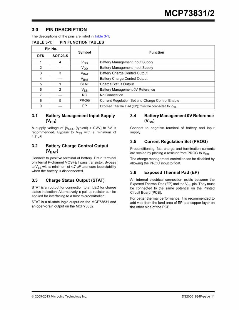
3.0 PIN DESCRIPTIONThe descriptions of the pins are listed in Table 3-1.
TABLE 3-1: PIN FUNCTION TABLES
3.1 Battery Management Input Supply (VDD)
A supply voltage of [VREG (typical) + 0.3V] to 6V isrecommended. Bypass to VSS with a minimum of4.7 µF.
3.2 Battery Charge Control Output (VBAT)
Connect to positive terminal of battery. Drain terminalof internal P-channel MOSFET pass transistor. Bypassto VSS with a minimum of 4.7 µF to ensure loop stabilitywhen the battery is disconnected.
3.3 Charge Status Output (STAT)
STAT is an output for connection to an LED for chargestatus indication. Alternatively, a pull-up resistor can beapplied for interfacing to a host microcontroller.
STAT is a tri-state logic output on the MCP73831 andan open-drain output on the MCP73832.
3.4 Battery Management 0V Reference (VSS)
Connect to negative terminal of battery and inputsupply.
3.5 Current Regulation Set (PROG)
Preconditioning, fast charge and termination currentsare scaled by placing a resistor from PROG to VSS.
The charge management controller can be disabled byallowing the PROG input to float.
3.6 Exposed Thermal Pad (EP)
An internal electrical connection exists between theExposed Thermal Pad (EP) and the VSS pin. They mustbe connected to the same potential on the PrintedCircuit Board (PCB).
For better thermal performance, it is recommended toadd vias from the land area of EP to a copper layer onthe other side of the PCB.
Pin No.Symbol Function
DFN SOT-23-5
1 4 VDD Battery Management Input Supply
2 — VDD Battery Management Input Supply
3 3 VBAT Battery Charge Control Output
4 — VBAT Battery Charge Control Output
5 1 STAT Charge Status Output
6 2 VSS Battery Management 0V Reference
7 — NC No Connection
8 5 PROG Current Regulation Set and Charge Control Enable
9 — EP Exposed Thermal Pad (EP); must be connected to VSS.
2005-2013 Microchip Technology Inc. DS20001984F-page 11

MCP73831/2
NOTES:
DS20001984F-page 12 2005-2013 Microchip Technology Inc.
MCP73831/2
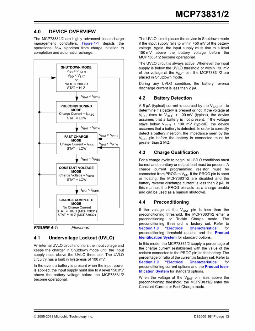
4.0 DEVICE OVERVIEWThe MCP73831/2 are highly advanced linear chargemanagement controllers. Figure 4-1 depicts theoperational flow algorithm from charge initiation tocompletion and automatic recharge.
FIGURE 4-1: Flowchart.
4.1 Undervoltage Lockout (UVLO)
An internal UVLO circuit monitors the input voltage andkeeps the charger in Shutdown mode until the inputsupply rises above the UVLO threshold. The UVLOcircuitry has a built in hysteresis of 100 mV.
In the event a battery is present when the input poweris applied, the input supply must rise to a level 150 mVabove the battery voltage before the MCP73831/2become operational.
The UVLO circuit places the device in Shutdown modeif the input supply falls to within +50 mV of the batteryvoltage. Again, the input supply must rise to a level150 mV above the battery voltage before theMCP73831/2 become operational.
The UVLO circuit is always active. Whenever the inputsupply is below the UVLO threshold or within +50 mVof the voltage at the VBAT pin, the MCP73831/2 areplaced in Shutdown mode.
During any UVLO condition, the battery reversedischarge current is less than 2 µA.
4.2 Battery Detection
A 6 µA (typical) current is sourced by the VBAT pin todetermine if a battery is present or not. If the voltage atVBAT rises to VREG + 100 mV (typical), the deviceassumes that a battery is not present. If the voltagestays below VREG + 100 mV (typical), the deviceassumes that a battery is detected. In order to correctlydetect a battery insertion, the impedance seen by theVBAT pin before the battery is connected must begreater than 2 MΩ.
4.3 Charge Qualification
For a charge cycle to begin, all UVLO conditions mustbe met and a battery or output load must be present. Acharge current programming resistor must beconnected from PROG to VSS. If the PROG pin is openor floating, the MCP73831/2 are disabled and thebattery reverse discharge current is less than 2 µA. Inthis manner, the PROG pin acts as a charge enableand can be used as a manual shutdown.
4.4 Preconditioning
If the voltage at the VBAT pin is less than thepreconditioning threshold, the MCP73831/2 enter apreconditioning or Trickle Charge mode. Thepreconditioning threshold is factory set. Refer toSection 1.0 “Electrical Characteristics” forpreconditioning threshold options and the ProductIdentification System for standard options.
In this mode, the MCP73831/2 supply a percentage ofthe charge current (established with the value of theresistor connected to the PROG pin) to the battery. Thepercentage or ratio of the current is factory set. Refer toSection 1.0 “Electrical Characteristics” forpreconditioning current options and the Product Iden-tification System for standard options.
When the voltage at the VBAT pin rises above thepreconditioning threshold, the MCP73831/2 enter theConstant-Current or Fast Charge mode.
SHUTDOWN MODEVDD < VUVLOVDD < VBAT
orPROG > 200 kΩ
STAT = Hi-Z
PRECONDITIONING MODE
Charge Current = IPREGSTAT = LOW
FAST CHARGE MODE
Charge Current = IREGSTAT = LOW
CONSTANT VOLTAGE MODE
Charge Voltage = VREGSTAT = LOW
VBAT < VPTH
VBAT > VPTH
VBAT = VREG
VBAT < VRTH
VBAT > VPTH
IBAT < ITERM
CHARGE COMPLETE MODE
No Charge CurrentSTAT = HIGH (MCP73831)STAT = Hi-Z (MCP73832)
2005-2013 Microchip Technology Inc. DS20001984F-page 13

MCP73831/2
4.5 Fast Charge Constant-Current Mode
During the Constant-Current mode, the programmedcharge current is supplied to the battery or load. Thecharge current is established using a single resistorfrom PROG to VSS. Constant-Current mode ismaintained until the voltage at the VBAT pin reaches theregulation voltage, VREG.
4.6 Constant-Voltage Mode
When the voltage at the VBAT pin reaches theregulation voltage, VREG, constant voltage regulationbegins. The regulation voltage is factory set to 4.2V,4.35V, 4.40V or 4.50V with a tolerance of ±0.75%.
4.7 Charge Termination
The charge cycle is terminated when, during Constant-Voltage mode, the average charge current diminishesbelow a percentage of the programmed charge current(established with the value of the resistor connected tothe PROG pin). A 1 ms filter time on the terminationcomparator ensures that transient load conditions donot result in premature charge cycle termination. Thepercentage or ratio of the current is factory set. Refer toSection 1.0 “Electrical Characteristics” for chargetermination current options and the ProductIdentification System for standard options.
The charge current is latched off and the MCP73831/2enter a Charge Complete mode.
4.8 Automatic Recharge
The MCP73831/2 continuously monitor the voltage atthe VBAT pin in the Charge Complete mode. If thevoltage drops below the recharge threshold, anothercharge cycle begins and current is once again suppliedto the battery or load. The recharge threshold is factoryset. Refer to Section 1.0 “Electrical Characteristics”for recharge threshold options and the ProductIdentification System for standard options.
4.9 Thermal Regulation
The MCP73831/2 limit the charge current based on thedie temperature. The thermal regulation optimizes thecharge cycle time while maintaining device reliability.Figure 4-2 depicts the thermal regulation for theMCP73831/2.
FIGURE 4-2: Thermal Regulation.
4.10 Thermal Shutdown
The MCP73831/2 suspend charge if the die tempera-ture exceeds 150°C. Charging will resume when thedie temperature has cooled by approximately 10°C.
0
75
150
225
300
375
450
525
25 35 45 55 65 75 85 95 105
115
125
135
145
155
Junction Temperature (°C)
Ch
arg
e C
urr
ent
(mA
)
RPROG = 2 kΩ
DS20001984F-page 14 2005-2013 Microchip Technology Inc.

MCP73831/2
5.0 DETAILED DESCRIPTION
5.1 Analog Circuitry
5.1.1 BATTERY MANAGEMENT INPUT SUPPLY (VDD)
The VDD pin is the input supply pin for the MCP73831/2 devices. The MCP73831/2 automatically enter aPower-Down mode if the voltage on the VDD input fallsbelow the UVLO voltage (VSTOP). This feature preventsdraining the battery pack when the VDD supply is notpresent.
5.1.2 CURRENT REGULATION SET (PROG)
Fast charge current regulation can be scaled by placinga programming resistor (RPROG) from the PROG inputto VSS. The program resistor and the charge currentare calculated using the following equation:
The preconditioning trickle charge current and thecharge termination current are ratiometric to the fastcharge current based on the selected device options.
5.1.3 BATTERY CHARGE CONTROL OUTPUT (VBAT)
The battery charge control output is the drain terminalof an internal P-channel MOSFET. The MCP73831/2provide constant current and voltage regulation to thebattery pack by controlling this MOSFET in the linearregion. The battery charge control output should beconnected to the positive terminal of the battery pack.
5.2 Digital Circuitry
5.2.1 STATUS INDICATOR (STAT)
The charge status output of the MCP73831 has threedifferent states: High (H), Low (L), and High-Impedance (Hi-Z). The charge status output of theMCP73832 is open-drain. It has two different states:Low (L) and High-Impedance (Hi-Z). The charge statusoutput can be used to illuminate one, two or tri-colorLEDs. Optionally, the charge status output can be usedas an interface to a host microcontroller.
Table 5-1 summarizes the state of the status outputduring a charge cycle.
5.2.2 DEVICE DISABLE (PROG)
The current regulation set input pin (PROG) can beused to terminate a charge at any time during thecharge cycle, as well as to initiate a charge cycle orinitiate a recharge cycle.
Placing a programming resistor from the PROG input toVSS enables the device. Allowing the PROG input tofloat or by applying a logic-high input signal, disablesthe device and terminates a charge cycle. Whendisabled, the device’s supply current is reduced to25 µA, typically.
IREG1000VRPROG-----------------=
Where:
RPROG = kOhms
IREG = milliampere
TABLE 5-1: STATUS OUTPUT
Charge Cycle State STAT1
MCP73831 MCP73832
Shutdown Hi-Z Hi-Z
No Battery Present Hi-Z Hi-Z
Preconditioning L L
Constant-Current Fast Charge
L L
Constant Voltage L L
Charge Complete – Standby
H Hi-Z
2005-2013 Microchip Technology Inc. DS20001984F-page 15

MCP73831/2
NOTES:
DS20001984F-page 16 2005-2013 Microchip Technology Inc.

MCP73831/2
6.0 APPLICATIONSThe MCP73831/2 are designed to operate inconjunction with a host microcontroller or in a stand-alone application. The MCP73831/2 provide thepreferred charge algorithm for Lithium-Ion and Lithium-Polymer cells. The algorithm uses a constant current
followed by a constant voltage charging method.Figure 6-1 depicts a typical stand-alone applicationcircuit, while Figure 6-2 and Figure 6-3 depict theaccompanying charge profile.
FIGURE 6-1: Typical Application Circuit.
FIGURE 6-2: Typical Charge Profile (180 mAh Battery).
FIGURE 6-3: Typical Charge Profile in Thermal Regulation (1000 mAh Battery).
6.1 Application Circuit Design
Due to the low efficiency of linear charging, the mostimportant factors are thermal design and cost, whichare a direct function of the input voltage, output currentand thermal impedance between the battery chargerand the ambient cooling air. The worst-case situation iswhen the device has transitioned from thePreconditioning mode to the Constant-Current mode.In this situation, the battery charger has to dissipate themaximum power. A trade-off must be made betweenthe charge current, cost and thermal requirements ofthe charger.
6.1.1 COMPONENT SELECTION
Selection of the external components in Figure 6-1 iscrucial to the integrity and reliability of the chargingsystem. The following discussion is intended as a guidefor the component selection process.
6.1.1.1 Current Programming Resistor (RPROG)
The preferred fast charge current for Lithium-Ion cellsis at the 1C rate, with an absolute maximum current atthe 2C rate. For example, a 500 mAh battery pack hasa preferred fast charge current of 500 mA. Charging atthis rate provides the shortest charge cycle timeswithout degradation to the battery pack performance orlife.
STAT
VDD
VSS
PROG
VBAT +
-
Single Li-Ion Cell
4
MCP73831
5
3
1
CIN
Li-Ion Battery Charger
2RPROG
RLED COUT
REGULATED WALL CUBE LED
0.0
1.0
2.0
3.0
4.0
5.0
6.0
0
20
40
60
80
100
120
140
160
180
Time (minutes)
Ba
tte
ry V
olt
age
(V)
0
20
40
60
80
100
120
Ch
arg
e C
urr
ent
(mA
)
MCP73831-2AC/IOTVDD = 5.2VRPROG = 10 kΩ
0.0
1.0
2.0
3.0
4.0
5.0
6.0
0
30
60
90
120
150
180
210
240
Time (minutes)
Bat
tery
Vo
ltag
e (V
)
0
100
200
300
400
500
600
Ch
arg
e C
urr
ent
(mA
)
MCP73831-2AC/IOTVDD = 5.2VRPROG = 2 kΩ
2005-2013 Microchip Technology Inc. DS20001984F-page 17

MCP73831/2
6.1.1.2 Thermal Considerations
The worst-case power dissipation in the batterycharger occurs when the input voltage is at themaximum and the device has transitioned from thePreconditioning mode to the Constant-Current mode.In this case, the power dissipation is:
Power dissipation with a 5V, ±10% input voltage sourceis:
This power dissipation with the battery charger in theSOT-23-5 package will cause thermal regulation to beentered as depicted in Figure 6-3. Alternatively, the2mm x 3mm DFN package could be utilized to reducecharge cycle times.
6.1.1.3 External Capacitors
The MCP73831/2 are stable with or without a batteryload. In order to maintain good AC stability in theConstant-Voltage mode, a minimum capacitance of4.7 µF is recommended to bypass the VBAT pin to VSS.This capacitance provides compensation when there isno battery load. In addition, the battery andinterconnections appear inductive at high frequencies.These elements are in the control feedback loop duringConstant-Voltage mode. Therefore, the bypasscapacitance may be necessary to compensate for theinductive nature of the battery pack.
Virtually any good quality output filter capacitor can beused, independent of the capacitor’s minimumEffective Series Resistance (ESR) value. The actualvalue of the capacitor (and its associated ESR)depends on the output load current. A 4.7 µF ceramic,tantalum or aluminum electrolytic capacitor at theoutput is usually sufficient to ensure stability for outputcurrents up to a 500 mA.
6.1.1.4 Reverse-Blocking Protection
The MCP73831/2 provide protection from a faulted orshorted input. Without the protection, a faulted orshorted input would discharge the battery pack throughthe body diode of the internal pass transistor.
6.1.1.5 Charge Inhibit
The current regulation set input pin (PROG) can beused to terminate a charge at any time during thecharge cycle, as well as to initiate a charge cycle orinitiate a recharge cycle.
Placing a programming resistor from the PROG input toVSS enables the device. Allowing the PROG input tofloat or by applying a logic-high input signal, disablesthe device and terminates a charge cycle. Whendisabled, the device’s supply current is reduced to25 µA, typically.
6.1.1.6 Charge Status Interface
A status output provides information on the state ofcharge. The output can be used to illuminate externalLEDs or interface to a host microcontroller. Refer toTable 5-1 for a summary of the state of the statusoutput during a charge cycle.
6.2 PCB Layout Issues
For optimum voltage regulation, place the battery packas close as possible to the device’s VBAT and VSS pins.This is recommended to minimize voltage drops alongthe high current-carrying PCB traces.
If the PCB layout is used as a heatsink, adding manyvias in the heatsink pad can help conduct more heat tothe PCB backplane, thus reducing the maximumjunction temperature. Figure 6-4 and Figure 6-5 depicta typical layout with PCB heatsinking.
FIGURE 6-4: Typical Layout (Top).
FIGURE 6-5: Typical Layout (Bottom).
PowerDissipation VDDMAX VPTHMIN–( ) IREGMAX×=
Where:
VDDMAX = the maximum input voltage
IREGMAX = the maximum fast charge current
VPTHMIN = the minimum transition threshold voltage
PowerDissipation 5.5V 2.7V–( ) 550mA× 1.54W= =
COUT
LED
RPROG
CINMCP73831
RLED
VBAT VDD
VSS
VBAT
VSS
VDD
DS20001984F-page 18 2005-2013 Microchip Technology Inc.

MCP73831/2
7.0 PACKAGING INFORMATION
7.1 Package Marking Information
Example
AAE73925
Device Code
MCP73831T-2ACI/MC AAE
MCP73831T-2ATI/MC AAF
MCP73831T-2DCI/MC AAG
MCP73831T-3ACI/MC AAH
MCP73831T-4ADI/MC AAJ
MCP73831T-5ACI/MC AAK
MCP73832T-2ACI/MC AAL
MCP73832T-2ATI/MC AAM
MCP73832T-2DCI/MC AAP
MCP73832T-3ACI/MC AAQ
MCP73832T-4ADI/MC AAR
MCP73832T-5ACI/MC AAS
Note: Applies to 8-Lead DFN
8-Lead DFN (2x3x0.9 mm)
Example
KD25
Device Code
MCP73831T-2ACI/OT KDNN
MCP73831T-2ATI/OT KENN
MCP73831T-2DCI/OT KFNN
MCP73831T-3ACI/OT KGNN
MCP73831T-4ADI/OT KHNN
MCP73831T-5ACI/OT KJNN
MCP73832T-2ACI/OT KKNN
MCP73832T-2ATI/OT KLNN
MCP73832T-2DCI/OT KMNN
MCP73832T-3ACI/OT KPNN
MCP73832T-4ADI/OT KQNN
MCP73832T-5ACI/OT KRNN
MCP73832T-2DFI/OT LUNN
Note: Applies to 5-Lead SOT-23
5-Lead SOT-23
XXNN
Legend: XX...X Customer-specific informationY Year code (last digit of calendar year)YY Year code (last 2 digits of calendar year)WW Week code (week of January 1 is week ‘01’)NNN Alphanumeric traceability code Pb-free Compliant JEDEC designator for Matte Tin (Sn)* This package is Pb-free. The Pb-free JEDEC designator ( )
can be found on the outer packaging for this package.
Note: In the event the full Microchip part number cannot be marked on one line, it will be carried overto the next line, thus limiting the number of available characters for customer-specificinformation.
3e
3e
2005-2013 Microchip Technology Inc. DS20001984F-page 19

MCP73831/2
!""#$%&
' !" #$ %! &'(!%&! %( % ")%% % " * & & # "% ( % " + * ) !% " & "% ,-.
/02 / & % #%! ))%!%% ,42 $ & '! !)%!%% '$$&%!
' 4% & %! %* ") ' % * $%% "%%%255)))&&5*
6% 99,,& 9&% : :; <
:!&( $ : =% ./0; > % = %"$$ .0%%* + ,4; 9 % /0; ?"% , +/0,# ""9 % + @ ..,# ""?"% , . @ .0%%?"% ( . +0%%9 % 9 + .0%%%,# "" F @ @
D
N
E
NOTE 1
1 2
EXPOSED PAD
NOTE 12 1
D2
K
L
E2
N
eb
A3 A1
A
NOTE 2
BOTTOM VIEWTOP VIEW
) 0+0
DS20001984F-page 20 2005-2013 Microchip Technology Inc.

MCP73831/2
Note: For the most current package drawings, please see the Microchip Packaging Specification located at http://www.microchip.com/packaging
2005-2013 Microchip Technology Inc. DS20001984F-page 21

MCP73831/2
( )"* +,-+ -*,%)*,&
' & ","%!" &"$ %! "$ %! % # "&& " & "% ,-.
/02 / & % #%! ))%!%%
' 4% & %! %* ") ' % * $%% "%%%255)))&&5*
6% 99,,& 9&% : :; <
:!&( $ : .9 "% ./0;!% " 9 "% /0; > % @ ." "* * = @ +%"$$ @ .; ?"% , @ +" "* ?"% , + @ =; 9 % @ +4%9 % 9 @ H4%% 9 +. @ =4% J @ +J9 "* = @ H9 "?"% ( @ .
φ
Nb
E
E1
D
1 2 3
e
e1
A
A1
A2 c
L
L1
) 0/
DS20001984F-page 22 2005-2013 Microchip Technology Inc.

MCP73831/2
Note: For the most current package drawings, please see the Microchip Packaging Specification located at http://www.microchip.com/packaging
2005-2013 Microchip Technology Inc. DS20001984F-page 23

MCP73831/2
DS20001984F-page 24 2005-2013 Microchip Technology Inc.
NOTES:

MCP73831/2
APPENDIX A: REVISION HISTORY
Revision F (June 2013)
The following is the list of modifications:
1. Updated the Functional Block Diagram.
2. Added the Battery Detection parameter andrelated information in the DC Characteristicstable.
3. Added new section Section 4.2 “BatteryDetection”.
4. Minor grammatical and spelling corrections.
Revision E (September 2008)
The following is the list of modifications:
1. Package Types: Changed DFN pinout dia-gram.
2. Section 1.0 “Electrical Characteristics”:Changed “Charge Impedance Range from20 kΩ to 67 kΩ.
3. Section 1.0 “Electrical Characteristics”:Misc. Formatting changes.
4. Section 2.0 “Typical Performance Curves”:Updated Figure 2-4.
5. Section 3.0 “Pin Description”: AddedExposed Pad pin to table and addedSection 3.6 “Exposed Thermal Pad (EP)”.
6. Updated Appendix A: “Revision History”
7. Added Land Pattern Package Outline Drawingfor 2x3 DFN package.
8. Pagination fixes throughout document perMarCom Standards.
Revision D (April 2008)
The following is the list of modifications:
1. Changed Charge Termination Current Ratio to8.5% minimum and 11.5% maximum.
Revision C (October 2007)
The following is the list of modifications:
1. Numerous edits throughout document.
2. Added note to Temperature Specificationstable.
3. Updated Figure 2-4.
Revision B (March 2006)
The following is the list of modifications:
1. Added MCP73832 through document.
Revision A (November 2005)
• Original Release of this Document.
2005-2013 Microchip Technology Inc. DS20001984F-page 25
MCP73831/2
NOTES:
DS20001984F-page 26 2005-2013 Microchip Technology Inc.

MCP73831/2
PRODUCT IDENTIFICATION SYSTEM
To order or obtain information, e.g., on pricing or delivery, refer to the factory or the listed sales office.
Device: MCP73831: Single-Cell Charge ControllerMCP73831T: Single-Cell Charge Controller
(Tape and Reel)MCP73832 Single-Cell Charge ControllerMCP73832T: Single-Cell Charge Controller
(Tape and Reel)
RegulationVoltage:
Code VREG
2 =3 =4 =5 =
4.20V4.35V4.40V4.50V
Options: * Code IPREG/IREG VPTH/VREG ITERM/IREG VRTH/VREG
ACADATDC
101010100
66.566.571.5
x
7.57.5207.5
96.59494
96.5
* Consult Factory for Alternative Device Options
Temperature Range:
I = -40°C to +85°C (Industrial)
Package: MC = Dual-Flat, No-Lead (2x3 mm body), 8-LeadOT = Small Outline Transistor (SOT23), 5-Lead
Examples: *
a) MCP73831-2ACI/OT: 4.20V VREG,Options AC, 5LD SOT23 Pkg
b) MCP73831T-2ACI/OT: Tape and Reel,4.20V VREG, Options AC, 5LD SOT23 Pkg
c) MCP73832-2ACI/MC: 4.20V VREG,Options AC, 8LD DFN Package
d) MCP73832T-2ACI/MC: Tape and Reel,4.20V VREG, Options AC, 8LD DFN Package
a) MCP73831-2ATI/OT: 4.20V VREG,Options AT, 5LD SOT23 Pkg
b) MCP73831T-2ATI/OT: Tape and Reel,4.20V VREG, Options AT, 5LD SOT23 Pkg
c) MCP73832-2ATI/MC: 4.20V VREG,Options AT, 8LD DFN Package
d) MCP73832T-2ATI/MC: Tape and Reel,4.20V VREG, Options AT, 8LD DFN Package
a) MCP73831-2DCI/OT: 4.20V VREG,Options DC, 5LD SOT23 Pkg
b) MCP73831T-2DCI/OT: Tape and Reel,4.20V VREG, Options DC, 5LD SOT23 Pkg
c) MCP73832-2DCI/MC: 4.20V VREG,Options DC, 8LD DFN Package
d) MCP73832T-2DCI/MC: Tape and Reel,4.20V VREG, Options DC, 8LD DFN Package
a) MCP73831-3ACI/OT: 4.35V VREG,Options AC, 5LD SOT23 Pkg
b) MCP73831T-3ACI/OT: Tape and Reel,4.35V VREG, Options AC, 5LD SOT23 Pkg
c) MCP73832-3ACI/MC: 4.35V VREG,Options AC, 8LD DFN Package
d) MCP73832T-3ACI/MC: Tape and Reel,4.35V VREG, Options AC, 8LD DFN Package
a) MCP73831-4ADI/OT: 4.40V VREG,Options AD, 5LD SOT23 Pkg
b) MCP73831T-4ADI/OT: Tape and Reel,4.40V VREG, Options AD, 5LD SOT23 Pkg
c) MCP73832-4ADI/MC: 4.40V VREG,Options AD, 8LD DFN Package
d) MCP73832T-4ADI/MC: Tape and Reel,4.40V VREG, Options AD, 8LD DFN Package
a) MCP73831-5ACI/OT: 4.50V VREG,Options AC, 5LD SOT23 Pkg
b) MCP73831T-5ACI/OT: Tape and Reel,4.50V VREG, Options AC, 5LD SOT23 Pkg
c) MCP73832-5ACI/MC: 4.50V VREG,Options AC, 8LD DFN Package
d) MCP73832T-5ACI/MC: Tape and Reel,4.50V VREG, Options AC, 8LD DFN Package
* Consult Factory for Alternate Device Options
PART NO.
Device
X
VREG
/XX
Package
XX
Options
X
TemperatureRange
2005-2013 Microchip Technology Inc. DS20001984F-page 27

MCP73831/2
NOTES:
DS20001984F-page 28 2005-2013 Microchip Technology Inc.

Note the following details of the code protection feature on Microchip devices:
• Microchip products meet the specification contained in their particular Microchip Data Sheet.
• Microchip believes that its family of products is one of the most secure families of its kind on the market today, when used in the intended manner and under normal conditions.
• There are dishonest and possibly illegal methods used to breach the code protection feature. All of these methods, to our knowledge, require using the Microchip products in a manner outside the operating specifications contained in Microchip’s Data Sheets. Most likely, the person doing so is engaged in theft of intellectual property.
• Microchip is willing to work with the customer who is concerned about the integrity of their code.
• Neither Microchip nor any other semiconductor manufacturer can guarantee the security of their code. Code protection does not mean that we are guaranteeing the product as “unbreakable.”
Code protection is constantly evolving. We at Microchip are committed to continuously improving the code protection features of ourproducts. Attempts to break Microchip’s code protection feature may be a violation of the Digital Millennium Copyright Act. If such actsallow unauthorized access to your software or other copyrighted work, you may have a right to sue for relief under that Act.
Information contained in this publication regarding deviceapplications and the like is provided only for your convenienceand may be superseded by updates. It is your responsibility toensure that your application meets with your specifications.MICROCHIP MAKES NO REPRESENTATIONS ORWARRANTIES OF ANY KIND WHETHER EXPRESS ORIMPLIED, WRITTEN OR ORAL, STATUTORY OROTHERWISE, RELATED TO THE INFORMATION,INCLUDING BUT NOT LIMITED TO ITS CONDITION,QUALITY, PERFORMANCE, MERCHANTABILITY ORFITNESS FOR PURPOSE. Microchip disclaims all liabilityarising from this information and its use. Use of Microchipdevices in life support and/or safety applications is entirely atthe buyer’s risk, and the buyer agrees to defend, indemnify andhold harmless Microchip from any and all damages, claims,suits, or expenses resulting from such use. No licenses areconveyed, implicitly or otherwise, under any Microchipintellectual property rights.
2005-2013 Microchip Technology Inc.
QUALITY MANAGEMENT SYSTEM CERTIFIED BY DNV
== ISO/TS 16949 ==
Trademarks
The Microchip name and logo, the Microchip logo, dsPIC, FlashFlex, KEELOQ, KEELOQ logo, MPLAB, PIC, PICmicro, PICSTART, PIC32 logo, rfPIC, SST, SST Logo, SuperFlash and UNI/O are registered trademarks of Microchip Technology Incorporated in the U.S.A. and other countries.
FilterLab, Hampshire, HI-TECH C, Linear Active Thermistor, MTP, SEEVAL and The Embedded Control Solutions Company are registered trademarks of Microchip Technology Incorporated in the U.S.A.
Silicon Storage Technology is a registered trademark of Microchip Technology Inc. in other countries.
Analog-for-the-Digital Age, Application Maestro, BodyCom, chipKIT, chipKIT logo, CodeGuard, dsPICDEM, dsPICDEM.net, dsPICworks, dsSPEAK, ECAN, ECONOMONITOR, FanSense, HI-TIDE, In-Circuit Serial Programming, ICSP, Mindi, MiWi, MPASM, MPF, MPLAB Certified logo, MPLIB, MPLINK, mTouch, Omniscient Code Generation, PICC, PICC-18, PICDEM, PICDEM.net, PICkit, PICtail, REAL ICE, rfLAB, Select Mode, SQI, Serial Quad I/O, Total Endurance, TSHARC, UniWinDriver, WiperLock, ZENA and Z-Scale are trademarks of Microchip Technology Incorporated in the U.S.A. and other countries.
SQTP is a service mark of Microchip Technology Incorporated in the U.S.A.
GestIC and ULPP are registered trademarks of Microchip Technology Germany II GmbH & Co. & KG, a subsidiary of Microchip Technology Inc., in other countries.
All other trademarks mentioned herein are property of their respective companies.
© 2005-2013, Microchip Technology Incorporated, Printed in the U.S.A., All Rights Reserved.
Printed on recycled paper.
ISBN: 978-1-62077-260-7
DS20001984F-page 29
Microchip received ISO/TS-16949:2009 certification for its worldwide headquarters, design and wafer fabrication facilities in Chandler and Tempe, Arizona; Gresham, Oregon and design centers in California and India. The Company’s quality system processes and procedures are for its PIC® MCUs and dsPIC® DSCs, KEELOQ® code hopping devices, Serial EEPROMs, microperipherals, nonvolatile memory and analog products. In addition, Microchip’s quality system for the design and manufacture of development systems is ISO 9001:2000 certified.

DS20001984F-page 30 2005-2013 Microchip Technology Inc.
AMERICASCorporate Office2355 West Chandler Blvd.Chandler, AZ 85224-6199Tel: 480-792-7200 Fax: 480-792-7277Technical Support: http://www.microchip.com/supportWeb Address: www.microchip.com
AtlantaDuluth, GA Tel: 678-957-9614 Fax: 678-957-1455
BostonWestborough, MA Tel: 774-760-0087 Fax: 774-760-0088
ChicagoItasca, IL Tel: 630-285-0071 Fax: 630-285-0075
ClevelandIndependence, OH Tel: 216-447-0464 Fax: 216-447-0643
DallasAddison, TX Tel: 972-818-7423 Fax: 972-818-2924
DetroitFarmington Hills, MI Tel: 248-538-2250Fax: 248-538-2260
IndianapolisNoblesville, IN Tel: 317-773-8323Fax: 317-773-5453
Los AngelesMission Viejo, CA Tel: 949-462-9523 Fax: 949-462-9608
Santa ClaraSanta Clara, CA Tel: 408-961-6444Fax: 408-961-6445
TorontoMississauga, Ontario, CanadaTel: 905-673-0699 Fax: 905-673-6509
ASIA/PACIFICAsia Pacific OfficeSuites 3707-14, 37th FloorTower 6, The GatewayHarbour City, KowloonHong KongTel: 852-2401-1200Fax: 852-2401-3431
Australia - SydneyTel: 61-2-9868-6733Fax: 61-2-9868-6755
China - BeijingTel: 86-10-8569-7000 Fax: 86-10-8528-2104
China - ChengduTel: 86-28-8665-5511Fax: 86-28-8665-7889
China - ChongqingTel: 86-23-8980-9588Fax: 86-23-8980-9500
China - HangzhouTel: 86-571-2819-3187 Fax: 86-571-2819-3189
China - Hong Kong SARTel: 852-2943-5100 Fax: 852-2401-3431
China - NanjingTel: 86-25-8473-2460Fax: 86-25-8473-2470
China - QingdaoTel: 86-532-8502-7355Fax: 86-532-8502-7205
China - ShanghaiTel: 86-21-5407-5533 Fax: 86-21-5407-5066
China - ShenyangTel: 86-24-2334-2829Fax: 86-24-2334-2393
China - ShenzhenTel: 86-755-8864-2200 Fax: 86-755-8203-1760
China - WuhanTel: 86-27-5980-5300Fax: 86-27-5980-5118
China - XianTel: 86-29-8833-7252Fax: 86-29-8833-7256
China - XiamenTel: 86-592-2388138 Fax: 86-592-2388130
China - ZhuhaiTel: 86-756-3210040 Fax: 86-756-3210049
ASIA/PACIFICIndia - BangaloreTel: 91-80-3090-4444 Fax: 91-80-3090-4123
India - New DelhiTel: 91-11-4160-8631Fax: 91-11-4160-8632
India - PuneTel: 91-20-2566-1512Fax: 91-20-2566-1513
Japan - OsakaTel: 81-6-6152-7160 Fax: 81-6-6152-9310
Japan - TokyoTel: 81-3-6880- 3770 Fax: 81-3-6880-3771
Korea - DaeguTel: 82-53-744-4301Fax: 82-53-744-4302
Korea - SeoulTel: 82-2-554-7200Fax: 82-2-558-5932 or 82-2-558-5934
Malaysia - Kuala LumpurTel: 60-3-6201-9857Fax: 60-3-6201-9859
Malaysia - PenangTel: 60-4-227-8870Fax: 60-4-227-4068
Philippines - ManilaTel: 63-2-634-9065Fax: 63-2-634-9069
SingaporeTel: 65-6334-8870Fax: 65-6334-8850
Taiwan - Hsin ChuTel: 886-3-5778-366Fax: 886-3-5770-955
Taiwan - KaohsiungTel: 886-7-213-7828Fax: 886-7-330-9305
Taiwan - TaipeiTel: 886-2-2508-8600 Fax: 886-2-2508-0102
Thailand - BangkokTel: 66-2-694-1351Fax: 66-2-694-1350
EUROPEAustria - WelsTel: 43-7242-2244-39Fax: 43-7242-2244-393Denmark - CopenhagenTel: 45-4450-2828 Fax: 45-4485-2829
France - ParisTel: 33-1-69-53-63-20 Fax: 33-1-69-30-90-79
Germany - MunichTel: 49-89-627-144-0 Fax: 49-89-627-144-44
Italy - Milan Tel: 39-0331-742611 Fax: 39-0331-466781
Netherlands - DrunenTel: 31-416-690399 Fax: 31-416-690340
Spain - MadridTel: 34-91-708-08-90Fax: 34-91-708-08-91
UK - WokinghamTel: 44-118-921-5869Fax: 44-118-921-5820
Worldwide Sales and Service
11/29/12