Embed Size (px)
Citation preview

Glasgow Theses Service http://theses.gla.ac.uk/
Mills, Gordon B. (1999) Scanning thermal microscopy using nanofabricated probes. PhD thesis. http://theses.gla.ac.uk/3134/ Copyright and moral rights for this thesis are retained by the author A copy can be downloaded for personal non-commercial research or study, without prior permission or charge This thesis cannot be reproduced or quoted extensively from without first obtaining permission in writing from the Author The content must not be changed in any way or sold commercially in any format or medium without the formal permission of the Author When referring to this work, full bibliographic details including the author, title, awarding institution and date of the thesis must be given

Scanning Thermal Microscopy Using Nanofabricated
Probes
by
Gordon B Mills
Submitted for the the Degree of Doctor of Philosophy
to the Faculty of Engineering at the University of Glasgow
September, 1999
© Gordon Mills 1999
Page 1

for Helen
Page 2

'Thanks 'To .
John Weaver glorious leader of the AFM group, championship
supervisor and top chum. For teaching me so much, for
shaving off his beard when I told him to, for losing
everything I ever gave him, and for always being on for
a cheeky babysham or two after the work was done.
Ashish Midha........................................ for putting in the groundwork which made all this
possible (just in time for me to arrive and steal the
glory).
Haiping Zhou for being the fabrication encyclopedia I never bought.
Lesley Donaldson.................................. for all the micromachined substrates and technical
support.
Nanoelectronics Research Centre the A-team - for the unrivalled expertise in e-beam
lithography and for providing such an enjoyable
environment to work in for four years.
Gari, Wei, Bridget, Juan, and Joe for technical support and social guidance while in
Phoenix.
The AFM group at Lancaster Uni. whose collaboration has been invaluable.
Family and friends.................................. for much support and encouragement.
Page 3
Abstract
Novel atomic force microscope (AFM) probes with integrated thin film thermal sensors
are presented. Silicon micromachining and high resolution electron beam lithography
(EBL) have been used to make batch fabricated, functionalised AFM probes. The AFM
tips, situated at the ends of Si3N4 cantilevers, are shaped either as truncated pyramids or
sharp triangular asperities. The former gives good thermalisation of the sensor to the
specimen for flat specimens whereas the latter gives improved access to highly
topographic specimens. Tip radii for the different probes are z 1 urn and 50 nm
respectively. A variety of metal structures have been deposited on the tips using EBL and
lift-off to form Au/Pd thermocouples and Pd resistance thermometer/heaters. Sensor
dimensions down to 35 nm have been demonstrated. In the case of the sharp triangular
tips, holes were etched into parts of the cantilever in order to provide self alignment of the
sensor to the tip. On the pyramidal tips it has been shown that multiple sensors can be
made on a single tip with good definition and matching between sensors.
A conventional AFM was constructed in order to test the micromachined thermal probes.
During scans of a photothermal test specimen using improved access thermocouple
probes, 80 nm period metal gratings were thermally resolved. This is equivalent to a
thermal lateral resolution of 40 nm. Pyramidal tips with a resistance thermometer/heater,
which were made for the microscopy and analysis of polymers, have been shown by
others to produce high resolution thermal conductivity images. The probes have also been
shown to be capable of locally heating a polymer specimen and thermomechanically
measuring phase changes in small volumes of material.
Also presented here is a study of scanning thermal microscopy of semiconductor
structures using a commercial AFM. Included are scans of several specimens using both
commercial andthe new micromachined probes. Subsurface images of voids buried under
a SiOz passivation layer were taken. It is shown that contrast caused by thermal
conductivity differences in the specimen may be detected at a depth of over 200 nm.
Page 4

Table of Contents
1 INTRODUCTION 7
1.1 SCANNING MICROSCOPES 7
1.2 ATOMIC FORCE MICROSCOPES 8
1.3 SCANNING THERMAL MICROSCOPES 10
1.4 PRIOR ART ATGLASGOW 14
1.5 MOTIVATION FOR WORK 16
2 GENERIC PROBE 23
2.1 FABRICATION TOOLS 23
2.2 ANALYSIS TOOLS 26
2.3 MICROMACHINED SUBSTRATE 27
2.4 3D LITHOGRAPHy 30
2.5 ADVANCED LIFT OFF 33
2.6 EVOLUTION OF GENERIC PROCESSING 35
3 INSTRUMENTATION 38
3.1 CONSTRUCTION OF AN AFM 38
3.2 AFM CONTROL ELECTRONICS 41
3.3 THERMOCOUPLE CIRCUITRY 44
4 THERMOCOUPLE PROBES 47
4.1 THERMOELECTRICITY 47
4.2 MATERIAL SySTEM 49
4.3 CROSS THERMOCOUPLES 50
4.4 TRIPLE THERMOCOUPLES 54
5 IMPROVED ACCESS THERMOCOUPLES 61
5.1 MOTIVATION 61
5.2 FABRICATION DEVELOPMENT 61
5.3 "SIDE" THERMOCOUPLE PROBES 66
5.4 PHOTOTHERMAL EXPERIMENT 69
5.5 "SWISS CHEESE" THERMOCOUPLES 72
6 RESISTANCE THERMOMETER PROBES 74
6.1 INTRODUCTION 74
6.2 EARLY WORK I PROBE CONTAMINATION 76
6.3 "BOWTIE" PROBES 78
Page 5

6.4 ENHANCED SENSITIVITY PROBES 83
6.5 SELF ALIGNED RESISTANCE PROBES 86
7 STUDIES AT CASE COLLABORATOR 91
7.1 INTRODUCTION 91
7.2 THERMAL PROBES 91
7.3 EXPERIMENTAL SETUP 93
7.4 PROBE CHARACTERISTICS 94
7.5 PASSIVATED WIRES 99
7.6 FIB TRENCHES 103
7.7 ANGLE CUT SPECIMEN 105
8 CONCLUSIONS 111
8.1 PROBE FABRICATION 111
8.2 MEASUREMENTS 113
8.3 ARTEFACTS 114
8.4 FUTURE WORK 116
9 PUBLICATIONS 120
Page 6

Chapter I - Introduction
1 Introduction
1.1 Scanning Microscopes
Many modern microscopy techniques are based on the concept of scanning including
scanning electron microscopy (SEM) [1], scanning optical microscopy [2], and scanning
probe microscopy (SPM) [3]. Research in the fields of material science [4], metallurgy
[5], biology [6], medicine [7] and semiconductor technology [8] has been furthered using
scanning microscopy. Measurements of such diverse properties as topography [9], ion
transport [10], electrical conductance [11], fluorescence [12] and spectroscopy of optical
emissions [13] have been made. The suitability of scanning microscopy to a wide range of
measurements and environments arises from the fact that the principle of the microscope is
in essence very simple. The idea is to sample information about the specimen at a number
of points (pixels) and then display the spatial variation of the data as an image. This is a
familiar and important way of visualising a specimen. Adding a scanner means that almost
any single point measurement can evolve into a microscopy technique. Many
measurements are made using sensors, probes or focused beams and these are particularly
suited to scanning microscopy.
A recent growth area has been the examination of specimen properties on the micro and
nano scale. This has been driven not only by research, but also by commercial activities in
biomedical, pharmaceutical and semiconductor sectors. Of particular interest are
l
I Tip Moves toMaintain Current
"-Conducting Specimen(Si <111> shown)
Figure 1-1 Schematic of a Scanning Tunneling Microscope.
Page 7

Chapter I - Introduction
microscopes that not only utilise the generic advantages of scanning, but also increase
image resolution using miniaturisation of the sensor. Miniaturisation down to the
molecular and atomic scale has only become possible in recent years following various
developments in micro and nano technology. Key to miniature scanning microscopes, for
example, is the use of piezoelectric transducers as nano-positioners [14], micromachining
[15] and advanced patterning techniques such as optical and electron lithography [16-18].
1.2 Atomic Force Microscopes
Atomic force microscopy (AFM) [19,20] is an innovative modification of the Nobel prize
winning scanning tunnelling microscopy (STM) developed in 1982 by Binnig, Rohrer,
Gerber and Weibel [21, 22]. Figure 1-1 shows a schematic of the STM, in which a sharp
tip is used to electrically probe a conducting specimen. A voltage is applied to the tip and
piezoelectric transducers used to bring the tip close to the specimen. When the spacing
between tip and specimen becomes sufficiently small (of order lOA) electrical tunnelling
across the gap takes place [23]. The tip is then mechanically scanned over the specimen
surface in a raster fashion, again using piezoelectric transducers. The tunnelling current is
extremely sensitive to the tip to specimen separation and varies as topographic features on
the specimen are encountered. Using a feedback loop to servo on the tunnelling current it
is possible to maintain the gap and detect height changes of order 0.01 A. The signal from
the feedback loop yields a topographic map of the specimen. Due to the extremely short
range interactions that determine the tunnelling current, the inventors were able to resolve
atoms of which a classic example is that of 7x7 silicon [24], shown in Figure 1-1. The
contrast mechanisms in STM are complex and beyond the scope of this text. A thorough
examination of the subject may be found elsewhere [3].
One drawback to the scanning tunnelling microscope however is that the specimen
necessarily has to be electrically conducting. Atomic force microscopy, shown
schematically in Figure 1-2, addresses this problem by mounting the sharp tip on a micro
cantilever. In this configuration, the tip to specimen distance is measured by detecting
cantilever deflections instead of tunnelling current. This means that non-conducting
specimens may be examined. The microscope tip can be operated in close proximity to the
surface, called non-contact mode, in which case long range forces (Vander Waals,
capillary, magnetic, electrostatic) cause attraction between tip and specimen [25].
Alternatively, the tip can be physically contacted to the specimen, called contact mode,
where screening forces cause repellent forces between tip and specimen [26, 27]. In both
cases the cantilever deflections must be detected with great accuracy, and this was
originally achieved by positioning an STM tip on the reverse of the cantilever. Modem
AFMs now commonly use optical techniques to detect cantilever deflections [3]. Atomic
Page 8

Chapter I - Introduction
Figure 1-2 Schematic of an Atomic Force Microscope.
scale resolution has also been observed using the AFM [28, 29], however since the
commercial availability of such instruments a key application has been measurements of
larger scale nano-roughness.
A third class of microscope, which evolved some years after the AFM, is called the
integrated sensor AFM. Here, microfabrication techniques are used to modify the AFM
cantilever to incorporate an additional sensor. The sensors perform a variety of different
functions. Some sensors have been used to replace the optical force sensing apparatus by
including a piezoresistive element on the cantilever [30]. Another invention, more
resembling the STM, used a micro-thermocouple to maintain tip to specimen separation by
measuring heat loss from a heated tip [31]. Simultaneous measurements of the
photothermal properties of the specimen were also made using this probe. A relatively
simple modification of silicon probes involves coating the tip with a ferromagnetic material
for magnetic imaging [32], or other conducting material for capacitive [33] and
conductance measurements [34]. More complex microfabricated probes have included
thermocouples for temperature mapping [35], fibre probes for high resolution optical
microscopy [36] and micropipette or micromachined probes for ion conductance
microscopy [10, 37]. Lithographic definition of sensors for SPM has been limited to a
small number of groups, the most successful of which developed the Hall bar microscope
for quantitative magnetic imaging [38].
Page 9

Chapter I - Introduction
1.3 Scanning Thermal Microscopes
Scanning thermal microscopy (SThM) is one of the new generation of integrated sensor
AFM techniques. Temperature sensors used have included metal thermocouples [39],
thermoresistors [40] and thermodiodes [41].
One of the first groups to incorporate a thermal sensor into the SPM environment was that
led by H.K. Wickramasinghe at IBM in New York [31]. The instrument was called the
scanning thermal profiler (STP) and operated by scanning a heated thermocouple junction,
situated at the end of a sharp tip, across a sample surface. When brought close to the
specimen, the thermocouple measured the rate of heat transfer into the specimen, and this
was used to regulate the height of the tip. The instrument was operated in a similar fashion
to an STM, using constant heat flow in place of constant tunnelling current, and hence was
not truly a dual contrast mode microscope. The lateral topographic resolution of this
instrument was reported as 0.1 urn.
A modified STP was developed by Oesterschultze et al at the University of Kassel,
Germany [42]. A thermocouple was formed by coating a sharp metal tip with epoxy resin
and then evaporating a second metal. Because the end of the metal tip remained uncoated
due to the surface tension of the epoxy film, the junction between the two metals is
localised to the tip apex. The size of the junction in this case covers an area 10 urn long at
the end of the tip. Lateral topographic resolution was claimed at less than 30 nm. Such a
small figure for resolution from such a large sensor is possible because the tip to
specimen contact area, which is confined to the very end of the probe, is the determining
factor.
Another thermal STM technique is the scanning tunnelling thermometer [43]. In this
configuration a metal tip is used to form a thermocouple with a dissimilar conducting
specimen. By plotting the thermoelectric voltage evolved when the tip to specimen junction
was externally heated using a laser, temperature maps relating to optical absorption were
produced. This technique proved to be unreliable in some cases because the thermocouple
coefficient varies with position when used with heterogeneous specimens (later used as a
contrast mechanism in scanning thermopower microscopy [44]). As with the STM, this
technique is limited to imaging conducting samples. With the work of Nonnenmacher et al
[45] this technology was transferred to the AFM environment. This instrument uses
attractive mode force sensing to bring a heated metal coated Si tip into near contact with
various metal specimens. Temperature is measured indirectly by detecting contact potential
variations in a similar way to the Kelvin probe microscope [46, 47]. The thermal
dependency arises from the temperature gradient formed between tip and specimen which,
Page 10

Chapter 1 - Introduction
depending on the proximity and thermal conductivity of the specimen, results in a change
in the contact potential. Thermal conductivity and subsurface images were produced, with
good correlation to the topographic features. Estimation of the exact temperature of the tip
was hampered by parasitic heating of the tip from the force sensing laser and domination
of a background signal level caused by the contact potential arising from the flat of the
cantilever and the specimen.
A leading group in integrated sensor AFM is that of A. Majumdar and co-workers who
work in the University of California, Santa Barbara. They have conducted a great deal of
research into microthermocouple fabrication. An early attempt involved two wires, one
chromel and one alumel, being fused together electrically and etched to form a sharp tip
[35]. An aluminium foil mirror was then glued to the back of the wires which were
mechanically twisted into a cantilever shape. The thermocouple junction size was
approximately 25 urrr'. One problem with this design however was that the tip tended to
deform with the force of contact. To solve this, a shard of diamond was glued to the probe
tip and one of its sharp facets scanned in place of the thermocouple [48]. Diamond has the
highest thermal conductivity of any material at room temperature, so the thermal time
constant of the instrument was not changed appreciably. An improvement in topographic
resolution was observed, however the thermal spatial resolution was still limited by the
thermocouple size. In addition to this, the probe characteristics were not reproducible
between scans since it proved impossible to identify and reuse a specific facet of the
diamond as the tip.
A different probe design by the same group featured a commercial silicon nitride cantilever
and tip which was coated in metal and used as a bimetallic strip [49]. The approach here
was to scan the cantilever in contact mode and measure temperature induced deflections,
due to the difference in expansion coefficients of the metal and the silicon nitride. It was
discovered that the deflection signal was dominated by heat convection in the air
surrounding the cantilever, and not by conduction through the tip. The instrument was
moved into vacuum and the tip radius increased by depositing a droplet of epoxy at the
end of the tip. Improved thermal images were obtained, albeit with reduced thermal spatial
resolution. The reported spatial resolution for topography was 1 nm with a corresponding
thermal spatial resolution of 0.4 urn. The group concluded that to reach 30-50 nm thermal
spatial resolution, the thermal sensor would have to be similarly sized [39].
Further efforts by the Majumdar group in producing extremely small thermocouples
involved processing commercial silicon nitride coated silicon cantilevers [50]. Here, the
silicon nitride was first stripped off and replaced by a thin layer of Au. On top of this, a
layer of silicon oxide was deposited followed by a thin layer of Pt. To pattern the sensor,
Page 11

Chapter I - Introduction
the tip was then brought into contact with a conducting surface and a voltage pulse of a
few Volts applied between the specimen and tip. The voltage pulse caused the thin Pt film
to evaporate around the point of contact, forming a small hole. After etching away the
underlying oxide, a capping layer of Pt was evaporated over the tip to form a thermocouple
junction equal in size to the hole at the end of the tip. Spatial resolution of the thermal
image was claimed to be 10 nm, however this was determined from the noise equivalent
spatial resolution of a single sharp edge caused by a spurious particle on the surface.
Noise equivalent spatial resolution is a calculation made by dividing the edge length of a
feature by the apparent signal to noise ratio in the image, and does not necessarily mean
that any such resolution (defined by the more conventional criteria) was demonstrated. A
disadvantage to this fabrication process was the unpredictable nature of the evaporation of
the Pt film, and the likelihood of contamination of the junction at this stage. The metals
were not always found to be in good contact and the thermocouple often did not last the
duration of a scan. Cantilever heating effects again produced artefacts in the thermal
images, because the front face of the cantilever was covered entirely in metal and therefore
a good thermal conductor.
Production of probes using this voltage induced evaporation lithography moved on to a
semi-batch process [51]. Shadow evaporation techniques were used to deposit metal pads
onto arrays of cantilevers. The devices were then separated and processed as before. The
group also made studies into the heat transfer mechanisms from tip to sample. They
concluded that at room temperature the main heat flow mechanism between tip and sample
was conduction through an aqueous separation layer.
The Kassel group have recently fabricated several different integrated sensor AFM probes
in batch processes [52-55]. They use micromachining of bulk silicon and gallium arsenide
[56] to produce wafers of around 200 tips. Their current thermal interests lie in fabrication
of Schottky diode probes [41] and scanning Joule expansion microscopy [57, 58]. The
Schottky diode probes use sharp conical tips with an approximately 250-500 nm active
region at the tip apex. Specimen access here is excellent, however the fact that only a small
fraction of the diode is in thermal contact with the sample could lead to any localised
thermal signal being overcome by ambient thermal noise and IIf noise in the sensor.
Besides thermal application of the probe, the diode is also sensitive to electrical and optical
fields.
The scanning Joule expansion technique was developed by the Kassel group in
collaboration with A. Majumdar. The technique uses cantilever deflection in a conventional
AFM probe to measure thermal expansion in a heated sample. Results have shown that
thermal expansions down to I pm can be detected.
Page 12

Chapter I - Introduction
An alternative to techniques where passive thermometers like thermocouples and diodes
are used to measure temperature, is SThM using resistance thermometers. These simple
thermometers can also heat the specimen, and therefore be used in an active stimulus /
response mode. The combination of resistance thermometry with AFM was first
demonstrated by Dinwiddie and co-workers [40], who micromechanically fashioned
miniature PtO.9RhO.l wires into a cantilever shape with a protruding tip. The Pto.9RhO.l wire
was 5 Il1Il in diameter with a 75 Il1Il Ag cladding. The cladding was removed around the
tip, increasing the probe resistance at the tip and also decreasing the tip dimensions. By
applying a small voltage to the resistive probe and measuring thermally induced resistance
changes, temperature changes at the tip can be detected. Alternatively, if a large current is
applied to the tip, significant heating can occur. Using the tip as a heat source, the heat
flow from tip to specimen can be measured. Applications for this technique include
localised calorimetry [59], thermal mapping of polymer blends [60], measurement of
thermal conductivities [61] and Fourier transform infra-red (FTIR) analysis of polymer
films [62]. In addition to these, several experiments have been carried out in the field of
sub-surface thermal imaging [63, 64]. It is possible to detect and estimate the depth of
subsurface features using resistive probes by modulating the electrical heating. Solution of
the one dimensional wave equation
where D is the thermal diffusivity of the specimen, T is temperature, x is the depth of
penetration and t is time, gives the thermal diffusion length, L, of the heat into the specimen
to be
L=~2:
This assumes periodic modulation of the heat source at angular frequency 0), that the tip
radius is infinitely large, and that conduction is the only heat transfer mechanism. In
reality, where a probe of finite tip radius is used, the problem is much more complex,
however this simple analysis shows that the depth of penetration may be controlled to
some degree by varying the modualtion frequency of the heat source. A more thorough
examination of the subject is given elsewhere [65].
One use for resistively heated thermal probes is in the field of AFM storage. Mamin et al
from IBM Almaden have achieved write densities of 10 Gb/in? at 100 kb/s [66] and read
rates of 1.2 Mb/s [67]. Initial strategies employed piezoresistive AFM cantilevers heated
using a focused infra-red laser [68] and then electrical heating of the whole cantilever [69]
Page 13
Chapter I - Introduction
to create nanoindentations in a polymer film. In order to decrease write times however the
thermal source needed to be reduced in size. This was achieved by selectively ion
implanting silicon cantilevers to leave a resistive region several microns wide at the tip
[66]. Thermal time constants of 30 us were observed compared to z 40 ms when heating
the whole cantilever. Such instruments may benefit from further miniaturisation of thermal
heaters and other innovations such as multiple cantilevers operated in parallel [70].
1.4 Prior Art at Glasgow
An initial study into using lithographic techniques to pattern sensors onto AFM tips was
carried out in 1993 by an undergraduate student at the University of Glasgow [71].
Results showed that recessed micromachined silicon tips could be coated with resist and
patterned using electron beam lithography (EBL). This discovery initiated a four year
effort to arrive at a generic technology for making integrated sensor AFM probes.
Funding was procured! and A. Midha, a postgraduate student, and Dr H. Zhou, a
postgraduate research assistant, were recruited to aid the development.
A design for batch fabricating integrated sensor AFM probes was developed 1993-1996,
and is described in full in the PhD thesis by A. Midha [72]. The principle of this design
was to provide a generic probe that would support multiple layers of lithography on and
around an AFM tip, thus allowing the fabrication of localised sensors. A variety of sensors
were envisioned including scanning near field optical microscopy (SNOM) apertures [73],
Hall Magnetometers [38] and thermometers. The goal was to advance these emerging
AFM techniques by shrinking sensor dimensions and improving the reproducibility and
stability of the integrated sensor probes.
Critical to this project was the availability of electron beam lithography at Glasgow
University. Photolithography [18] and silicon etching [74] is routinely used to batch
fabricate sharp tips for topographic mapping [15], but attempts to combine lithography
and micromachining to make integrated sensor probes have encountered alignment and
resolution limits on the micron scale [51]. Using EBL brings the ability to pattern features
and automatically align on the nanometer scale [17, 75, 76].
Figure 1-3 shows a schematic of an individual cantilever as proposed by A. Midha et al.
Layers which defined the sensor at the tip apex are patterned on a silicon nitride cantilever
supported on a silicon membrane. Probe bases, alignment marks, cantilevers and tips are
all defined by etching a single silicon wafer and so the probes are monolithic in nature (see
1 9/1994-8/1996, EPSRC, "Nanofabrication of scanned probe microscope sensors", £212k, GRJK24307
Page 14

Device at Apex
\
Metal Tracks
MicromachinedPyramid Tip
Cantilever
/ SiSubstrate
Chapter I - Introduction
ToBondPads
Figure 1-3 Schematic of a generic AFM cantilever.
Chapter 2). This served to overcome many historical difficulties encountered when trying
to add sensors to AFM cantilevers. Adapting planar semiconductor techniques to a custom
made 3-dimensional substrate became the task, as opposed to processing a fragile free
standing cantilever.
After several iterative design modifications to achieve the maximum device quantity per
wafer, but with suitable substrate resilience, the generic substrate emerged as a 3" silicon
wafer containing 240 "blank" probes, ready for EBL modification. The wafer was
designed to be cleaved into quarters before sensor definition to aid speedy process
development, but all processing was designed to be compatible with the use of 3" wafers.
Although batch fabrication of probes lends itself readily to mass production for
commercial purposes, this was not the original motivation of the inventors. Rather, the
primary objective was to provide a supply of near identical probes for research purposes.
It was hoped that this would add stability and continuity to integrated sensor AFM
experiments, and also provide a technology base for producing more complex probes (e.g.
combined sensors on a single probe).
The situation at the start of this project was that a scheme for fabricating wafers of probes
ready for EBL modification had been developed. Sensor technology was less well
advanced. Most of the effort by A. Midha had been directed at producing probes with
integrated apertures for SNOM. However, problems involving the pattern transfer of the
Page 15

Chapter I - Introduction
apertures and subsequent metal cladding had delayed progress substantially. The
patterning of metal features to produce thermal devices had already been demonstrated on
flat test specimens and Dr H. Zhou was actively involved in furthering this work to three
dimensional substrates.
Summarising, the current state of technology inherited at the beginning of the project
comprised:
• Etching of a commercially available three inch silicon wafer to form batch fabricated
probe bases.
• Through wafer alignment markers for use with EBL.
• A timed silicon etch to form pyramidal tips.
• "Float coating" - a novel resist scheme for coating three dimensional features [77].
• Software implementation for automatic refocusing of the Leica EBL machine for
writing patterns on substrates with significant relief.
• A KOH etch resistant material system for patterning metal features on the end of
pyramid tips.
• A final silicon release etch for dissolving the supporting membrane to leave free
standing AFM cantilevers.
1.5 Motivation for Work
Building on the work of the AFM group at the University of Glasgow, this project was
focused on the advancement of the technology for generic, batch fabricated, integrated
sensor AFM probes. The motivation was to use the technology to produce thermal probes
for high resolution SThM. The specific goals were to develop the existing fabrication
processes to give reproducible working probes, to explore the characteristics of the new
probes, and to scan specimens which would demonstrate their enhanced capabilities. The
manufacture of the probes remained core, however unlike other predominantly fabrication
based projects the application of the technology was a top priority.
The fabrication aims of the project were as follows:
• Use EBL to pattern thermal sensors on the generic cantilevers designed by A. Midha.
• Increase the yield of probes to produce many identical probes.
• Address the problem of poor specimen access inherent to the existing probes.
The benefits of using EBL to make integrated sensor probes are threefold. Firstly, EBL is
a tool that can typically produce features of order 50 nm. If implemented successfully this
Page 16

Chapter I - Introduction
would improve significantly on current SThM sensor miniaturisation. Secondly, the
automation used with such tools allows many levels to be accurately aligned to the AFM
tip. This differs from most other "punctual" techniques where a single event (electrical
evaporation or fusion, non-continuity of resist, chemical etching, micromanipulation)
localises the sensor to the tip apex. The benefits of lithographic definition are that sensors
may become more complex by adding multiple levels, and have much smaller feature
dimensions. Lastly, the excellent reproducibility offered by EBL means that sensors will
vary less from probe to probe. Currently, probes tend to be individually characterised
before use and each experiment is then unique to that probe.
Emerging analytical techniques on the nanometer scale are of considerable interest to the
semiconductor industry, and as such this project attracted sponsorship from Motorola
MRST 2. The sponsorship was in the form of an Engineering and Physical Sciences
Research Council (EPSRC) Co-operative Award in Science in Engineering (CASE). Due
to a need for new microscopic techniques with which to examine ever shrinking
generations of integrated circuit, the project was supported both financially and with
expertise in the areas of microscopy and material characterisation. Part of the sponsorship
involved an extended period of work at the Materials Characterisation Lab in Mesa,
Arizona (see Chapter 7). The objective was to assess SThM by examining semiconductor
devices and related structures. Some of the perceived applications of SThM to Motorola
were as follows.
• Thermal detection of local heat distributions III densely populated very large scale
integrated (VLSI) devices.
• Identification of electrical faults which result in thermal features.
• Detection of subsurface elements of multilayer structures.
• Non-invasive inspection of packaged devices with passivation coatings.
• Profiling the optical output of semiconductor lasers.
Additional motivation for the development of thermal probes was provided by an informal
collaboration between the University of Glasgow an the University of Lancaster, England.
The group in the Department of Physics in Lancaster, headed by Dr H. M. Pollock, are
experts in thermal microscopy of polymers. Using resistance thermometer probes,
pioneering work has resulted in the invention of CASM (calorimetric analysis with
scanning microscopy) and MASM (mechanothermal analysis with scanning microscopy)
[78]. Improvements on the current Wollaston wire technology were anticipated in the form
2 Materials Research and Strategic Technologies, Motorola SPS, 2200 West Broadway Rd, Mesa, Arizona85202
Page 17

Chapter i-introduction
of increased thermal imaging resolution, improved response time and decreased analysis
volumes.
[1] Light and Electron Microscopy: Cambridge University Press, 1992.
[2] J. B. Pawley, Handbook ofBiological Confocal Microscopy. New York: Plenum Press, 1990.
[3] Scanning probe microscopy and spectroscopy: Cambridge University Press, 1994.
[4] S. Amelinckx, R. Gevers, and J. Van Landuyt, Diffraction and Imaging Techniques in MaterialScience, vol. 1: North Holland Publishing Company, 1978.
[5] Metallurgical Microscopy: Butterworth, 1973.
[6] A. M. Baro, R. Miranda, J. A1aman, N. Garcia, G. Binnig, H. Rohrer, C. Gerber, and J. L.Carrascosa, "Determination of surface-topography of biological specimens at high- resolution byscanning tunnelling microscopy," Nature, vol. 315, pp. 253-254, 1985.
[7] Electron microscopy in human medicine, vol. 1-11: McGraw Hill, 1978-1983.
[8] S. M. Sze, VLSI Technology: McGraw Hill, 1988.
[9] G. Binnig and H. Rohrer, "Surface imaging by scanning tunneling microscopy,"Ultramicroscopy, vol. 11, pp. 157-160, 1983.
[10] C. B. Prater, P. K. Hansma, M. Tortonese, and C. F. Quate, "Improved scanning ionconductance microscope using microfabricated probes," Review Of Scientific Instruments, vol.62, pp. 2634-2638, 1991.
[11] A. Olbrich, B. Ebersberger, and C. Boit, "Conducting atomic force microscopy for nanoscaleelectrical characterization of thin Si02," Applied Physics Letters, vol. 73, pp. 3114-3116, 1998.
[12] Fluorescent Probes in Cellular and Molecular Biology: CRC Press, 1994.
[13] R. C. Davis and C. C. Williams, "Nanometer-scale absorption-spectroscopy by near-fieldphotodetection optical microscopy," Applied Physics Letters, vol. 69, pp. 1179-1181, 1996.
[14] G. Binnig and D. P. E. Smith, "Single-tube 3-dimensional scanner for scanning tunnelingmicroscopy," Review Of Scientific Instruments, vol. 57, pp. 1688-1689, 1986.
[15] T. R. Albrecht, S. Akamine, T. E. Carver, and C. F. Quate, "Microfabrication of cantilever stylifor the atomic force microscope," Joumal Of Vacuum Science & Technology a-Vacuum Surfacesand Films, vol. 8, pp. 3386-3396, 1990.
[16] S. P. Beaumont, P. G. Bower, T. Tamamura, and C. D. W. Wilkinson, "Sub-20-nm-wide metallines by electron-beam exposure of thin poly(methyl methacrylate) films and liftoff," AppliedPhysics Letters, vol. 38, pp. 436-439, 1981.
[17] R. F. W. Pease, "Electron-beam lithography," Contemporary Physics, vol. 22, pp. 265-290,1981.
[18] B. J. Lin, "Deep uv lithography," Journal Of Vacuum Science & Technology, vol. 12, pp.1317-1320, 1975.
[19] G. Binnig, C. F. Quate, and C. Gerber, "Atomic force microscope," Physical Review Letters,vol. 56, pp. 930-933, 1986.
Page 18

Chapter I - Introduction
[20] G. Binnig, "Force microscopy," Ultramicroscopy, vol. 42, pp. 7-15, 1992.
[21] G. Binnig, H. Rohrer, C. Gerber, and E. Weibel, "Tunneling through a controllable vacuumgap," Applied Physics Letters, vol. 40, pp. 178-180, 1982.
[22] G. Binnig and H. Rohrer, "Scanning tunneling microscopy," Helvetica Physica Acta, vol. 55,pp. 726-735, 1982.
[23] G. Binnig, H. Rohrer, C. Gerber, and E. Weibel, "Vacuum tunneling," Physica B&C, vol. 110,pp. 2075-2077, 1982.
[24] G. Binnig, H. Rohrer, C. Gerber, and E. Weibel, "7X7 Reconstruction on si(111) resolved inreal space," Physical Review Letters, vol. 50, pp. 120-123, 1983.
[25] M. Nonnenmacher, J. Greschner, O. Wolter, and R. Kassing, "Scanning force microscopy withmicromachined silicon sensors," Journal Of Vacuum Science & Technology B, vol. 9, pp. 13581362, 1991.
[26] The Solid State: Oxford Science Publications, 1978.
[27] Solid State Physics: Cambridge University Press, 1974.
[28] G. Binnig, C. Gerber, E. Stoll, T. R. Albrecht, and C. F. Quate, "Atomic resolution withatomic force microscope," Surface Science, vol. 189, pp. 1-6, 1987.
[29] F. Ohnesorge and G. Binnig, 'True atomic-resolution by atomic force microscopy throughrepulsive and attractive forces," Science, vol. 260, pp. 1451-1456, 1993.
[30] M. Tortonese, R. C. Barrett, and C. F. Quate, "Atomic resolution with an atomic forcemicroscope using piezoresistive detection," Applied Physics Letters, vol. 62, pp. 834-836, 1993.
[31] C. C. Williams and H. K. Wickramasinghe, "Scanning thermal profiler," Applied PhysicsLetters, vol. 49, pp. 1587-1589, 1986.
[32] P. Grutter, E. Meyer, H. Heinzelmann, L. Rosentha1er, H. R. Hidber, and H. J. Guntherodt,"Magnetic imaging by atomic force microscope," Journal Of Applied Physics, vol. 63, pp.2947-2947, 1988.
[33] C. C. Williams, W. P. Hough, and S. A. Rishton, "Scanning capacitance microscopy on a 25nm scale," Applied Physics Letters, vol. 55, pp. 203-205, 1989.
[34] A. Born, A. Olbrich, M. Maywald, and R. Wiesendanger, "Analysis of electrical breakdownfailures by means of SFM-based methods," Applied Physics a-Materials Science & Processing,vol. 66, pp. S1063-S1065, 1998.
[35] A. Majumdar, 1. P. Carrejo, and 1. Lai, "Thermal imaging using the atomic force microscope,"Applied Physics Letters, vol. 62, pp. 2501-2503, 1993.
[36] E. Betzig, S. G. Grubb, R. J. Chichester, D. J. Digiovanni, and J. S. Weiner, "Fiber laser probefor near-field scanning optical microscopy," Applied Physics Letters, vol. 63, pp. 3550-3552,1993.
[37] P. K. Hansma, B. Drake, O. Marti, S. A. C. Gould, and C. B. Prater, "The scanning ionconductance microscope," Science, vol. 243, pp. 641-643, 1989.
[38] A. Oral, S. J. Bending, and M. Henini, "Scanning Hall probe microscopy of superconductors andmagnetic materials," Journal Of Vacuum Science & Technology B, vol. 14, pp. 1202-1205,1996.
Page 19

Chapter 1 - Introduction
[39] A. Majumdar, J. Lai, M. Chandrachood, o. Nakabeppu, Y. Wu, and Z. Shi, "Thermal imagingby atomic-force microscopy using thermocouple cantilever probes," Review Of ScientificInstruments, vol. 66, pp. 3584-3592, 1995.
[40] R. B. Dinwiddie, R. J. Pyllki, and P. E. West, "Thermal conductivity contrast imaging with ascanning thermal microscope," in Thermal Conductivity, T. W. Tong, Ed., 1994, pp. 22.
[41] T. Leinhos, M. Stopka, and E. Oesterschulze, "Micromachined fabrication of Si cantilevers withSchottky diodes integrated in the tip," Applied Physics a-Materials Science & Processing, vol.66, pp. S65-S69, 1998.
[42] M. Stopka, L. Hadjiiski, E. Oesterschulze, and R. Kassing, "Surface investigations by scanningthermal microscopy," Journal Of Vacuum Science & Technology B, vol. 13, pp. 2153-2156,1995.
[43] J. M. R. Weaver, L. M. Walpita, and H. K. Wickramasinghe, Applied Physics Letters, vol. 49,pp. 1587, 1989.
[44] 1. Xu, B. Koslowski, R. Moller, K. Lauger, K. Dransfeld, and 1. H. Wilson, "Proposal to studythe thermopower produced by a vacuum-tunneling junction," Journal Of Vacuum Science &Technology B, vol. 12, pp. 2156-2160, 1994.
[45] M. Nonnenmacher and H. K. Wickramasinghe, "Scanning probe microscopy of thermalconductivity and subsurface properties," Applied Physics Letters, vol. 61, pp. 168-170, 1992.
[46] M. Nonnenmacher, M. P. Oboyle, and H. K. Wickramasinghe, "Kelvin probe forcemicroscopy," Applied Physics Letters, vol. 58, pp. 2921-2923, 1991.
[47] J. M. R. Weaver and D. W. Abraham, "High-resolution atomic force microscopypotentiometry," Journal Of Vacuum Science & Technology B, vol. 9, pp. 1559-1561, 1991.
[48] J. Lai, M. Chandrachood, A. Majumdar, and J. P. Carrejo, "Thermal detection of device failureby atomic-force microscopy," Ieee Electron Device Letters, vol. 16, pp. 312-315,1995.
[49] o. Nakabeppu, M. Chandrachood, Y. Wu, J. Lai, and A. Majumdar, "Scanning thermal imagingmicroscopy using composite cantilever probes," Applied Physics Letters, vol. 66, pp. 694-696,1995.
[50] K. Luo, Z. Shi, J. Lai, and A. Majumdar, "Nanofabrication of sensors on cantilever probe tipsfor scanning multiprobe microscopy," Applied Physics Letters, vol. 68, pp. 325-327, 1996.
[51] K. Luo, Z. Shi, J. Varesi, and A. Majumdar, "Sensor nanofabrication, performance, andconduction mechanisms in scanning thermal microscopy," Journal Of Vacuum Science &Technology B, vol. 15, pp. 349-360, 1997.
[52] S. Munster, S. Werner, C. Mihalcea, W. Scholz, and E. Oesterschulze, "Novel micromachinedcantilever sensors for scanning near-field optical microscopy," Journal Of Microscopy-Oxford,vol. 186, pp. 17-22, 1997.
[53] E. Oesterschulze, W. Scholz, C. Mihalcea, D. Albert, B. Sobisch, and W. Kulisch, "Fabricationof small diamond tips for scanning probe microscopy application," Applied Physics Letters, vol.70, pp. 435-437, 1997.
[54] E. Oesterschulze and M. Stopka, "Imaging of thermal-properties and topography by combinedscanning thermal and scanning-tunneling-microscopy," Microelectronic Engineering, vol. 31, pp.241-248, 1996.
Page 20
Chapter I - Introduction
[55] C. Mihalcea, W. Scholz, S. Werner, S. Munster, E. Oesterschulze, and R. Kassing,"Multipurpose sensor tips for scanning near-field microscopy," Applied Physics Letters, vol. 68,pp. 3531-3533, 1996.
[56] S. Heisig and E. Oesterschu1ze, "Gallium arsenide probes for scanning near-field probemicroscopy," Applied Physics a-Materials Science & Processing, vol. 66, pp. S385-S390, 1998.
[57] S. Munster, T. Chang, R. Kassing, A. Majumdar, and E. Oesterschulze, "Micromachined Probesfor High Frequency Scanning Electrical Force Microscopy and Scanning Joule ExpansionMicroscopy," Pre-Print, 1997.
[58] J. Varesi and A. Majumdar, "Scanning Joule expansion microscopy at nanometer scales,"Applied Physics Letters, vol. 72, pp. 37-39, 1998.
[59] A. Hammiche, M. Reading, H. M. Pollock, M. Song, and D. J. Hourston, "Localized thermalanalysis using a miniaturized resistive probe," Review Of Scientific Instruments, vol. 67, pp.4268-4274, 1996.
[60] A. Hammiche, D. J. Hourston, H. M. Pollock, M. Reading, and M. Song, "Scanning thermalmicroscopy - subsurface imaging, thermal mapping of polymer blends, and localizedcalorimetry," Journal Of Vacuum Science & Technology B, vol. 14, pp. 1486-1491, 1996.
[61] L. 1. Balk, M. Maywald, and R. J. Pylkki, "Nanoscopic detection of the thermal-conductivity ofcompound semiconductor-materials by enhanced scanning thermal microscopy," Institute OfPhysics Conference Series, vol. 146, pp. 655-658, 1995.
[62] A. Hammiche, H. M. Pollock, M. Reading, M. Claybourn, P. H. Turner, and K. Jewkes,"Photothermal FT-IR spectroscopy: A step towards FT-IR microscopy at a resolution better thanthe diffraction limit," Applied Spectroscopy, vol. 53, pp. 810-815, 1999.
[63] A. Hammiche, H. M. Pollock, M. Song, and D. J. Hourston, "Subsurface imaging by scanningthermal microscopy," Measurement Science & Technology, vol. 7, pp. 142-150, 1996.
[64] A. Hamrniche, M. Song, H. M. Pollock, M. Reading, and D. J. Hourston, "Subsurface sthmimaging of blends, with localized calorimetric analysis," Abstracts Of Papers Of the AmericanChemical Society, vol. 212, pp. 278-POLY, 1996.
[65] D. Almond, and P. Patel, Photothermal Science and Techniques: Chapman and Hall, 1996.
[66] B. W. Chui, T. D. Stowe, Y. S. Ju, K. E. Goodson, T. W. Kenny, H. J. Mamin, B. D. Terris,R. P. Ried, and D. Rugar, "Low-stiffness silicon cantilevers with integrated heaters andpiezoresistive sensors for high-density AFM thermomechanical data storage," Journal OfMicroelectromechanical Systems, vol. 7, pp. 69-78, 1998.
[67] B. W. Chui, T. D. Stowe, T. W. Kenny, H. J. Mamin, B. D. Terris, and D. Rugar, "Lowstiffness silicon cantilevers for thermal writing and piezoresistive readback with the atomic forcemicroscope," Applied Physics Letters, vol. 69, pp. 2767-2769, 1996.
[68] H. J. Mamin and D. Rugar, "Thermomechanical writing with an atomic force microscope tip,"Applied Physics Letters, vol. 61, pp. 1003-1005, 1992.
[69] H. J. Mamin, "Thermal writing using a heated atomic force microscope tip," Applied PhysicsLetters, vol. 69, pp. 433-435, 1996.
[70] S. C. Minne, S. R. Manalis, and C. F. Quate, "Parallel atomic force microscopy usingcantilevers with integrated piezoresistive sensors and integrated piezoelectric actuators," AppliedPhysics Letters, vol. 67, pp. 3918-3920, 1995.
Page 21

Chapter I - Introduction
[71] S. Rahman, "Final year project in E&EE," , vol. supervised by Dr J.M.R. Weaver, pp.University of Glasgow, 1994.
[72] A. Midha, "Batch-fabrication of novel nanoprobes for SPM," in Electronics & ElectricalEngineering. Glasgow: University of Glasgow, submission due 1999.
[73] E. Betzig, A. Harootunian, A. Lewis, and M. Isaacson, "Near-field scanning optical microscopy(nsom) - investigation of radiation transmitted through sub-wavelength apertures," BiophysicalJournal, vol. 47, pp. A407-A407, 1985.
[74] K. R. Williams and R. S. Muller, "Etch rates for micromachining processing," Journal OfMicroelectromechanical Systems, vol. 5, pp. 256-269, 1996.
[75] A. N. Broers, W. W. Molzen, J. J. Cuomo, and N. D. Wittels, "Electron beam fabrication of 80A metal structures," Applied Physics Letters, vol. 29, pp. 596-598, 1976.
[76] A. N. Broers, J. M. E. Harper, and W. W. Molzen, "250-A linewidths with PMMA electronresist," Applied Physics Letters, vol. 33, pp. 392-394, 1978.
[77] A. Midha, L. Donaldson, G. Mills, J. M. R. Weaver, and H. Zhou, ""Float Coating": A ResistCoating Technique for Electron-Beam Nanolithography on Micromachined Substrates,"Unpublished, 1997.
[78] M. Reading, D. J. Hourston, M. Song, H. M. Pollock, and A. Hammiche, "Thennal analysisfor the 21st century," American Laboratory, vol. 30, pp. 13, 1998.
Page 22

Chapter 2 - Generic Probe
2 Generic Probe
2.1 Fabrication Tools
A contact printer (by Hybrid Technology Group) was used for all of the photolithographic
micromachining stages. This type of photolithography uses a shadow mask to produce
optical images on a substrate. The mask is physically contacted to a surface and exposed
with UV light. A photosensitive coating (Microposit' S1818), which is a positive resist, is
used as the imaging medium. The developer for this resist is AZ14003 (1:1
developer:water). Minimum feature sizes down to 250 nm have been demonstrated using
contact printing techniques [1], however for routine work over large areas a minimum
feature size of 500 nm is commonplace. Different photolithographic levels were manually
aligned using this machine with placement errors of approximately 10 11m.
Electron beam lithography (EEL) was performed using a Leica' EEPG 5HR machine.
This machine is a 100 kV vector scan model with a five inch, interferometrically
positioned, stage. Vector scanning differs from simpler raster scanning in that the writing
beam is directed only to the areas of the substrate to be exposed and so reduces writing
times for sparse patterns. The writing fields are 800x800 11m with typical stitching
accuracies of 50 nm. Minimum spot size is 12 nm at 100 kV which gives written feature
sizes down to 25 nm. Patterns are held in software and are designed using a program
called Wavemaker (WAM) which produces GDSII pattern files (an industry standard
format). Write times are typically a few hours long depending on pattern density and dose.
The machine is routinely run at both 50 kV and 100 kV. In general 50 kV (high beam
current, larger spot sizes) is used for low resolutionllarge coverage patterns whereas 100
kV (low beam current, small spot sizes) is used for high resolution/small coverage
patterns. The EEL machine is run with two different final aperture sizes (see Figure 2-1),
large for 50 kV and small for 100 kV. This results in the electron beam having a better
spot shape and greater depth of focus for 100 kV operation (at the expense of beam
current) compared to 50 kV. Jobs times at 100 kV are roughly two to three times longer
than equivalent jobs written at 50 kV.
PMMA (poly-methyl methacrylate) resists were used for all the electron beam work
during this investigation. Two different varieties, Aldricli' (120,000 mwt) and Elvacite'
3 Shipley, Humber Ave, Trading Estate, Coventry, UK.4 Leica Lithography Systems, Clifton Rd, Cambridge, CB1 3QH.5 Barnard Microsystems Ltd.6 Aldrich Chemicals Co. Ltd, The Old Brickyard, New Rd, Gillingham, Dorset, SP8 4JL.7 Elvacite - brand name belonging to Dupont.
Page 23

Chapter 2 - Generic Probe
LJElectron Gun
Aperture
Condenser Lens
Blanking Plates
Beam Shaping Lenses
Aperture
Stigmators
Deflection Coils
Final Lens
Final Aperture
Figure 2-1 Representation of an electron
lithography system.
(350,000 mwt) dissolved in orthoxylene were available. The resists were spun onto the
substrates using commercial spinners at speeds of 2500 or 5000 rpm depending on the
nature of the specimen. Concentrations of 2.5% up to 12% resist by weight were available
in each variety of resist giving film thicknesses in the range 20 to 500 nm.
Typically the lithographic patterns for the probe fabrication were transferred into metal
device layers, or metal masks for reactive ion etching (RIE). Metal deposition was carried
out in an automatic Plassys' MEB 450 evaporator. Six different metals (Au, Pd, Ni, NiCr,
Ge, Ti) were available using this machine. The Plassys heats the metals using an electron
gun (10 kV, 1 A) under a vacuum of lx l O" Torr and the thickness is measured with an
accuracy of approximately 1 nm using a crystal detector. Specimen and metal source are
situated approximately one metre apart in this evaporator which gives minimal heating of
the specimen. This is important when the specimen is patterned with polymers such as
PMMA which can reflow at 180°C. Sputter coating was also used during the process to
deposit Cr. This method uses a plasma to sputter atoms from a metal disc which then
condense on the specimen to form a film of uniform thickness [2].
8 Plassys, 14 Rue de la Gare, 91630 Marolles-en-Harepoix, France.
Page 24

Chapter 2 - Generic Probe
Pattern transfer from resist into metal was achieved by using wet etching (Cr and NiCr) or
"lift off" (Au, Pd, NiCr, Ti). Lift off is a technique whereby metal is evaporated directly
onto a specimen after resist development [3]. Areas where the resist has cleared out allow
the metal to stick to the specimen, but in all other areas the metal is removed as the
underlying resist is dissolved in acetone.
Bulk silicon micromachining is used to define the probe bases, cleave lines, markers and
pyramidal tips on the generic substrate. Accurate timed etching was achieved by using a
custom made etching kit comprising 750 ml Quickfit reaction flask, Eurotherm'
temperature controller, twin Pt thermometer, Electrothermal heating mantle (with magnetic
stirring) and water cooled reflux. Machined steel (corrosion resistant grade 3l6-S3l)
formed a two piece cover for the reaction flask which allowed access for a three inch
wafer. KOH is an anisotropic etch for silicon etch stopping on the <111> plane for
concave etch pits. The KOH solution was made by dissolving KOH pellets into ultrapure
water to make 7 molar solution (increased by 5% due to compensate for potassium
carbonate formation in air). For this solution, temperatures of 80-105 °C gave etch rates
between 75±1 um/hour and 255±1 um/hr in the <100> direction. In order to etch convex
features (like a pyramidal tip) a mixture of KOH + IPA (isopropyl alcohol) was used.
Although the IPA is not miscible in KOH solution and forms a separate layer on top of
the alkali, it changes the etch rate of certain fast etching silicon planes [4] which produces
a desirable tip profile for convex pyramids [5].
RIB is routinely used to transfer metal and polymer patterns into silicon nitride. The metal
masks are patterned using either photolithography, or electron beam lithography followed
by lift off or wet etching. Using a Plasma Technologies'? BP80 machine with C2F6 gas
(15 mTorr, 100 W), silicon nitride is etched at rates about 30 nrn/min using a bias of -300
V.
Sacrificial dielectric layers were required during the micromachining process and, although
the starting substrates were precoated on both sides with 100 nm thick silicon nitride
deposited by low pressure chemical vapour deposition (LPCVD), it was necessary to
perform dielectric deposition at Glasgow. The available resources dictated that plasma
enhanced chemical vapour deposition (PECVD) silicon nitride was used. This form of
silicon nitride is formed by reacting silane and ammonia gases in a glow discharge over a
heated stage (300-350 0C). The resultant coating is high in hydrogen and oxygen
9 Eurotherm Ltd, Faraday Close, Durrington, Worthing, W Sussex, BN13 3PL, UK.10 Plasma Technology Ltd, North End, Yatton, Bristol, Avon BS19 4AP, UK.
Page 25

Chapter 2 - Generic Probe
impurities and its properties differ from LPCVD silicon nitride in some respects (e.g. low
resistance to hydrofluoric acid) yet remain similar in others (e.g. RIB rate using CzF6).
Stress in PECVD nitride layers can be created during deposition and may relax later when
the layer is micromachined. Stress of this nature is undesirable when making micro-levers
such as AFM cantilevers and so the deposition parameters were optimised minimise stress
[6].
2.2 Analysis Tools
Scanning electron microscopes were used routinely during this investigation. In all cases
Hitachi" machines were used (S800, S900, S4500). All microscopes used field emission
sources and were operated at a variety of accelerating voltages. Wafers of probes were
examined after most steps in the fabrication process in order to check the quality of the
lithography or etching. Normally only a few sites on the wafer were examined because of
the possibility of contamination from oil in the chamber. It was found that a very low
voltage (3 kV or below) was needed when imaging released Si3N4 cantilevers because the
cantilever would bend due to charging. Even using low accelerating voltages, charging of
the Si3N4 cantilever caused the image contrast to vary.
Leica'", Nikon'? and Zeiss'" epi-illumination optical microscopes were used for the optical
analysis of large scale features on specimens and probes. Image capture using CCD
cameras was available and examples can be seen in later chapters. Nomarski interference
contrast was used with some of the specimens to enhance topographic contrast.
A Digital Instruments'? atomic force microscope was used during part of this
investigation. The microscope was capable of being used in both contact, tapping and lift
modes. A modification to the electronics and scanning head allowed resistive thermal tips
to be used. Sharp commercial silicon and silicon nitride AFM probes were also used for
verifying the topographic images acquired with the blunter probes.
A Micrion" focused ion beam system was used for both drilling holes in thermal
specimens, and imaging metal grains. Implantation of gallium was a concern when
preparing thermal specimens, because this can change the thermal properties of the
11 Hitachi Scientific Instr, Merlin BId, Hogwood Ind Est, Finchhamstead, Wokingham, Berks, UK.12 Leica Microsystems Holdings GmbH, Ernst-Leitz-Strasse, D-35578 Wetzlar, Germany.13 Nikon UK, Haybrook, Halesfield 9, Telford, Shropshire TF2 4EW, UK.14 Carl Zeiss lena GmbH, Zeiss Gruppe, Tatzendpromenade la, 07745 lena, Germany.15 Digital Instruments, 112 Robin Hill Rd, Santa Barbara CA, USA.16 Micrion Corporation, One Corporation Way, Centennial Park, Peabody, MA 01960-7990, USA.
Page 26

n-Si, (100) >Silicon Nitride100nmthick----------
Chapter 2 - Generic Probe
- Define through alignmentholes in nitride usingPhotoli1hog-aphy I Dryetch, Wet etch silicontooum deep
\(\
~ r- Similarly definehole in____--',...\! ~:~~~~~h will become
_ Etch through alignment_ ...... ........._ marksto completion.
Define AFM tips.
\ I Define EBLalignment---, ,r--- \ r--~ marksat sametime,
] [2StripremainingSiliconNitrideDeposit low stress Silicon
LA.AJ-"'U"--'lr""--...-AJIL...l V Nitride to form cantilever.
Perform multiplelevels of EBLon silicon nitridesurface to form device.
Etch Siliconmembranetorelease the cantilevers.
Figure 2-2 Micromachining levels from raw material to release.
specimen. A procedure of implanting a broad area before milling specific sites was
recommended to equalise this effect [7].
Scanning Auger spectroscopy was performed to identify the contamination level of
materials on a commercial thermal probe. The Physical Electronics'! machine was
operated by B. Rogers of Motorola. Scanning Auger is routinely used for identifying light
elements like oxygen, carbon and sodium. It was necessary in this case to use a sputtering
beam to clean excess carbon from specimen surfaces before analysis.
2.3 Micromachined Substrate
The probe fabrication process for a generic probe is shown schematically in Figure 2-2.
Initial KOH silicon etches on the reverse side of the wafer form individual probe bases
and a thin silicon membrane. Photolithography masks for these levels were produced
using electron beam lithography. Figure 2-3 shows WAM designs for the masks, and a
processed wafer after the reverse side micromachining has been completed. All subsequent
Page 27

(a) (b)
Chapter 2 - Generic Probe
(c)
Figure 2-3 (a) CAD pattern for 1st photolithography mask containing cleave lines, etch through
markers and course alignment markers. (b) CAD pattern for 2nd photolithography mask containing probe
bases and membranes. (c) Photograph of wafer after etching of the 2nd photolithography pattern.
front side patterns are written directly onto the wafer using EBL. In order to align the front
side EBL patterns to the micromachined probe bases and membranes, markers are
patterned during the reverse side processing. Timing of the KOH etches then produces
holes etched through the wafer to which the electron beam writer can align.
The first electron beam lithography level on the front side contains patterns for the
SiliconMembrane
CrackArrestor
SensorLayers
Used LocalMarker
Figure 2-4 SEM of the front side of the micromachined substrate.
17 Physical Electronics, www.phi.com.
Page 28
Chapter 2 - Generic Probe
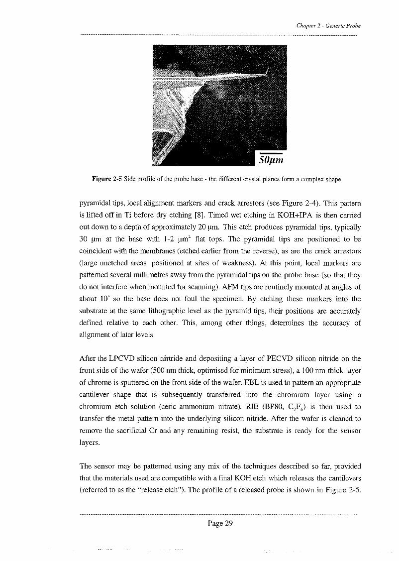
Figure 2-5 Side profile of the probe base - the different crystal planes form a complex shape.
pyramidal tips, local alignment markers and crack arrestors (see Figure 2-4). This pattern
is lifted off in Ti before dry etching [8]. Timed wet etching in KOH+IPA is then carried
out down to a depth of approximately 20 11m. This etch produces pyramidal tips, typically
30 11m at the base with I-211m2 flat tops. The pyramidal tips are positioned to be
coincident with the membranes (etched earlier from the reverse), as are the crack arrestors
(large unetched areas positioned at sites of weakness). At this point, local markers are
patterned several millimetres away from the pyramidal tips on the probe base (so that they
do not interfere when mounted for scanning). AFM tips are routinely mounted at angles of
about 10° so the base does not foul the specimen. By etching these markers into the
substrate at the same lithographic level as the pyramid tips, their positions are accurately
defined relative to each other. This, among other things, determines the accuracy of
alignment of later levels.
After the LPCVD silicon nirtride and depositing a layer of PECVD silicon nitride on the
front side of the wafer (500 nm thick, optimised for minimum stress), a 100 nm thick layer
of chrome is sputtered on the front side of the wafer. EBL is used to pattern an appropriate
cantilever shape that is subsequently transferred into the chromium layer using a
chromium etch solution (eerie ammonium nitrate). RIB (BP80, C2F6) is then used to
transfer the metal pattern into the underlying silicon nitride. After the wafer is cleaned to
remove the sacrificial Cr and any remaining resist, the substrate is ready for the sensor
layers.
The sensor may be patterned using any mix of the techniques described so far, provided
that the materials used are compatible with a final KOH etch which releases the cantilevers
(referred to as the "release etch"). The profile of a released probe is shown in Figure 2-5.
Page 29
Chapter 2 - Generic Probe
Note that the probe base is a complex shape due to the combined etching from front and
back.
2.4 3D Lithography
Formation of reproducible sensors at the end of sharp tips was the main goal of this
project, and several techniques specific to Glasgow had been developed to achieve this. Dr
J. Weaver, A. Midha, Dr H. Zhou and Dr S. Thoms were the inventors of this technology
which served to overcome problems encountered when using high resolution EBL to make
the sensors. Problems involving resist coating, alignment, and focusing of the EBL tool
were addressed.
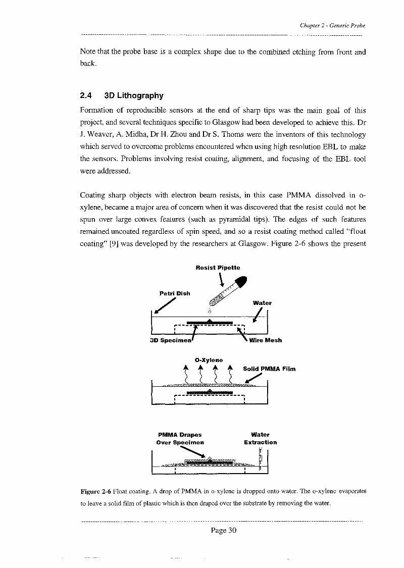
Coating sharp objects with electron beam resists, in this case PMMA dissolved in 0
xylene, became a major area of concern when it was discovered that the resist could not be
spun over large convex features (such as pyramidal tips). The edges of such features
remained uncoated regardless of spin speed, and so a resist coating method called "float
coating" [9] was developed by the researchers at Glasgow. Figure 2-6 shows the present
Resist Pipette
\Petri Dish
./ ii, Water
I~ . I' If----t---t-------,~ i
3D Specimenr " Wire Mesh
O.Xylene
t ~ t t Solid PM) ) ( ( /
•r-----------------~I I
MAFilm
PMMA DrapesOver Specimen
<,Water
Extraction
Figure 2-6 Float coating. A drop of PMMA in o-xylene is dropped onto water. The o-xylene evaporates
to leave a solid film of plastic which is then draped over the substrate by removing the water.
Page 30

Chapter 2 - Generic Probe
technique used to float coat specimens, which was used for most of the work described in
this document. The specimen is submerged in a dish of ultrapure water and a single drop
ofPMMA dissolved in o-xylene is allowed to fall onto the water surface. The o-xylene is
immiscible in water and quickly spreads out over the water surface. Using water at room
temperature, the o-xylene evaporates in I to 2 minutes leaving a continuous solid film of
PMMA floating in the water surface. The size and thickness of the solid film is dependent
on the concentration of PMMA and the dynamics of the drying process [10]. As the
ultrapure water is then slowly removed, the film approaches the specimen and ultimately
drapes over the specimen surface. Both flat and micromachined areas are coated with
resist. In particular, the sharp edges of micromachined features (e.g. pyramidal tips) are
well coated. Problems with "wrinkles" in the solid PMMA film have been observed. The
density of the wrinkles appear to be dependent on the environmental conditions during
evaporation of the o-xylene (e.g. temperature, air flow, humidity). A bake for 30 mins at
180°C after the float coating removes any residual water from the specimen surface and
takes the PMMA through its glass transition where it reflows to some extent and many
wrinkles are removed. Some wrinkles do remain however and Figure 2-7 shows a
potentially devastating wrinkle on a pyramidal tip. Although these wrinkles do not in
general cause lithographic failure, this may be because the patterns used for the thermal
sensors are sparsely distributed. Float coating may not be suitable for dense patterns.
Figure 2-7 Plan view of a micromachined pyramid which has been coated using
float coating. A random wrinkle has coincided with the tip in this case and could
potentially affect further processing.
Page 31
Chapter 2 - Generic Probe
Problems encountered when performing EBL on specimens with significant relief are
varied. Refocusing the EBL machine is necessary in order to write a well resolved pattern
away from the substrate plane. This involved modification of the control software and
changes in the pattern to multiple matrices written at different focus. 100 kV operation was
used for all writing away from the substrate plane because it provides greater depth of
focus. An added benefit of using 100 kV was that the smallest writing spot (12 nm) was
available for the sensor levels.
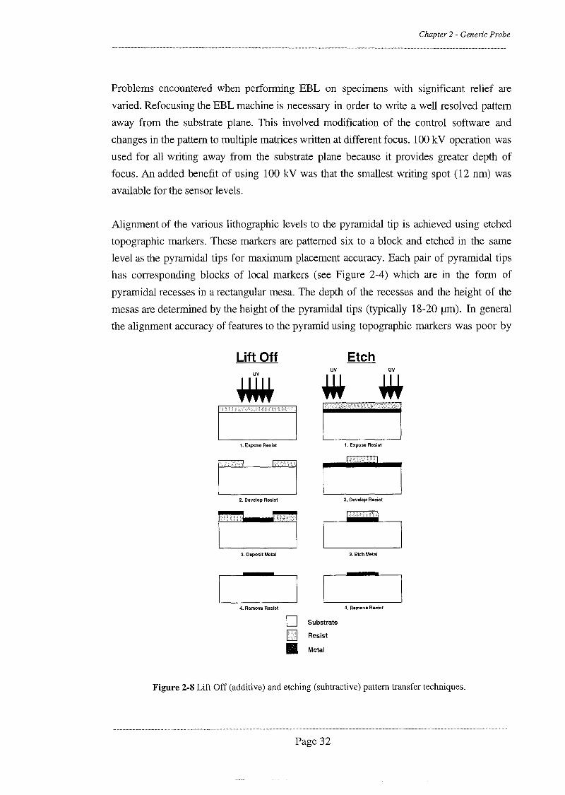
Alignment of the various lithographic levels to the pyramidal tip is achieved using etched
topographic markers. These markers are patterned six to a block and etched in the same
level as the pyramidal tips for maximum placement accuracy. Each pair of pyramidal tips
has corresponding blocks of local markers (see Figure 2-4) which are in the form of
pyramidal recesses in a rectangular mesa. The depth of the recesses and the height of the
mesas are determined by the height of the pyramidal tips (typically 18-20 um). In general
the alignment accuracy of features to the pyramid using topographic markers was poor by
Lift Off Etchuv
~uv uv
#t tf+
I I
2. Develop Resist
1. Expose Resist 1. Expose Resist
L""~2. Develop Resistr , L'''''·'''''"'''"~
3. Deposit Metal 3. Etch Metal
_11-4. Remove Resist
o Substrate
o Resist
• Metal
4. Remove Resist
Figure 2-8 Lift Off (additive) and etching (subtractive) pattern transfer techniques.
Page 32

Chapter 2 - Generic Probe
EEL standards ("" 250 nm). Problems with alignment of features will be discussed in more
detail in Chapter 5.
2.5 Advanced Lift Off
Metal lift off was routinely used at the sensor definition levels of the process. In general,
lift off will preserve high resolution features during pattern transfer better than etching
processes (Figure 2-8). This is because etching tends to remove material laterally as well
as vertically which causes shrinking and rounding of fine features. Lift off, in contrast, is
used to remove metal which has been evaporated vertically onto the substrate and so the
pattern should be perfectly preserved. Theoretically, removal of metal during lift off is a
trivial and consistent process because there is no physical attachment between the metal
(a)400nIn
(b)
Figure 2-9 (a) Undercut resist profile with 200 nm of metal evaporated on top. (b)
Overcut resist profile with 200 nm of metal evaporated on top. Note how the metal
film is continuous in (b) but not in (a). Micrographs courtesy of Fraser Williamson,
University of Glasgow.
pattern which stays on the substrate and the surplus metal which is removed. In practise
the removal of surplus metal is far from trivial and unwanted pieces of metal (called
"flags") often fail to detach from the exposed features. The reason for poor lift off is that
vertical resist profiles are difficult to achieve. Depending on development conditions, resist
profiles can vary from undercut (desirable) to overcut (undesirable). Figure 2-9 shows
examples of different metalised resist profiles. Where the resist profile is overcut, the
metal film is continuous and may cause flags. The metal film however is weaker at the
joins, and so when the underlying resist is removed, the surplus metal can tear away giving
successful lift off. Conventional methods which improve lift off include physical agitation
using ultrasonic bursts or "shooting" using micropipettes (a manual technique [3]).
Page 33

Chapter 2 - Generic Probe
The problem of poor development causing flags is acute for the lift off of the sensor levels
positioned on the micromachined pyramidal tips. Different matrices in the EBL patterns
are written to be in focus only on the substrate plane and at the tip apex, and so the
electron beam is imperfectly focused on the sides of the pyramids where the matrices
overlap. The result of this is that trivial feature growth is observed on the sides of the
pyramids and the electron dose at feature edges is reduced due to broadening of the
writing spot. Optimum development of this pattern is difficult to achieve because of the
variations in dose over the pyramid. Flags and metal caps on the pyramids are common.
An additional lift off aid for 3D substrates was developed involving the patterning of
sacrificial features which facilitate the tearing mechanism of metal removal. These
sacrificial features take a variety of forms depending on the nature of the pattern. For
example, it was observed that lift off of a single metal wire bisecting a micromachined
pyramid was in general successful. It was also observed that if a wire was patterned up the
pyramid and terminated near the apex, then in general the metal failed to lift off from the
pyramid apex and formed a cap (see Section 5.2 for further information).
Three examples of sacrificial features which improve lift off on pyramidal tips are shown
in Figure 2-10. In Figure 2-1O(b) a triple thermocouple device is shown where three Pd
wires bisect a single Au wire at the apex of a pyramidal tip. Spatial constraints affected
how many pads for electrical connection may be patterned, and so each of the four wires is
single terminal. Instead of terminating the wires at the pyramid apex, the wires extend over
to the other side of the pyramid. After some pattern optimisation (see Chapter 4) lift off
yield for this complex pattern approached 90% and virtually eliminated occurrences of
cappmg.
(a) (b) (c)
Figure 2-10 (a) Triple thermocouple probe. (b) Triangular cantilever shape for an improved access
probe. (c) An improved access thermocouple probe pre-release.
Page 34

Chapter 2 - Generic Probe
Figure 2-1O(b) shows a sharp triangular shape lifted off in metal on the side of a
pyramidal tip. The purpose of the metal is to mask underlying silicon nitride during RIB.
The silicon nitride that remains after etching forms the AFM cantilever. An "L" shaped
feature has been patterned here at the tip apex to aid lift off. This feature provides an extra
region where the metal on the tip may tear, and it was found that lift off of the triangular
feature was greatly improved. Although the "L" shaped feature remains after RIB etching,
it floats away in the release etch because it has no attachment to the cantilever.
A final example is shown in Figure 2-1O(c). Here, the thermocouple wires for a probe have
to coincide with a triangular shaped cantilever on the side of a pyramidal tip. In similar
fashion to the triple thermocouple device, the wires are not terminated on the pyramid (as
was first intended), but are extended over to the opposite side. This time the wires do not
run over the tip apex, but nevertheless improved lift off yield significantly.
2.6 Evolution of Generic Processing
Several advances in the fabrication of the generic probe were made during this project, the
most important of which were as follows. Firstly, a capping layer was introduced after the
cantilever definition layer. This was to offset the fact that despite being an isotropic form
of metal coating, the sputtered Cr film that formed the dry etch mask was not continuous.
The film appeared not to cover the apices of the pyramids and formed a star shaped hole
like that shown in Figure 2-11. After dry etching, the unprotected silicon nitride at the tip
apex was etched, which rendered the cantilever useless for further modification. The
capping layer consisted of an extra, low resolution, level of lithography consisting of a
square over the pyramidal tip. This pattern was lifted off in thin Nio.6Cr0.4 to form an extra
Figure 2-11 SEM of the apex of a pyramidal tip coated with 100 nm Cr. Note the
star shapes region which has remained uncoated.
Page 35

Chapter 2 - Generic Probe
(a) (b)Figure 2-12 (a) Cantilever released in KOH. (b) Cantilever released in KOH+IPA. Arrowed regions
show where the silicon base has receded badly with etch (a) but not with etch (b).
dry etch protection layer for the affected area. The use of thicker Cr layers, or a bilayer of
sputtered and evaporated metal, may eventually result in the elimination of this process.
The release etch was also changed during the lifetime of this project. Exact timing of the
KOH release etch was required to ensure that the probe base receded to exactly the bottom
of the cantilever. A top priority however was to ensure that all the silicon had been
removed from inside the pyramidal tip, and so the probes were often deliberately over
etched. Figure 2-12(a) shows a released probe that has been undercut, resulting in a
weakened cantilever. This often led to cracks evolving at the base of the cantilever due to
the lateral forces experienced during AFM scanning. In order to alleviate the problem, Dr
H. Zhou substituted the KOH with a KOH/IPA etch solution similar to that used in the
pyramid etch. This etch solution was known to slow the etch rates of certain fast etching
planes in silicon [4], and the resulting profile showed a marked improvement over the pure
KOH solution. Figure 2-12(b) shows a cantilever released in the KOHIIPA solution. Note
the squarer profile of the silicon at the cantilever base, which gives enhanced lateral
stiffness and reduced stress concentration at the cantilever base.
[1] B. J. Lin, "Deep uv lithography," Journal Of Vacuum Science & Technology, vol. 12, pp.1317-1320,1975.
[2] S. M. Sze, VLSI Technology: McGraw-Hill, 1988.
Page 36
Chapter 2 - Generic Probe
[3] S. P. Beaumont, P. G. Bower, T. Tamamura, and C. D. W. Wilkinson, "Sub-20-nm-wide metallines by electron-beam exposure of thin poly(methyl methacrylate) films and liftoff," AppliedPhysics Letters, vol. 38, pp. 436-439, 1981.
[4] K. R. Williams and R. S. Muller, "Etch rates for micromachining processing," Journal OfMicroelectromechanical Systems, vol. 5, pp. 256-269, 1996.
[5] A. Midha, "Batch-fabrication of novel nanoprobes for SPM," in Electronics & ElectricalEngineering. Glasgow: University of Glasgow, submission due 1999.
[6] S. Hicks, "Low stress PECVD silicon nitride.," University of Glasgow, Personalcommunication, [email protected].
[7] G. Harris, Motorola MRST, Private communication 1998, [email protected].
[8] A. Midha, S. K. Murad, and J. M. R. Weaver, "Anisotropic pattern transfer of fine resist featuresto silicon nitride via an intermediate titanium layer," Microelectronic Engineering, vol. 35, pp.99-102, 1997.
[9] A. Midha, L. Donaldson, G. Mills, J. M. R. Weaver, and H. Zhou, ""Float Coating": A ResistCoating Technique for Electron-Beam Nanolithography on Micromachined Substrates,"Unpublished, 1997.
[10] P. Ball, "Fluid dynamics - How coffee leaves its mark," Nature, vol. 389, pp. 788, 1997.
Page 37

Chapter 3 - Instrumentation
3 Instrumentation
3.1 Construction of an AFM
A flexible microscope was built for the testing and scanning of the functionalised AFM
probes. Initial design and construction was performed by Dr J. Weaver and A. Midha.
Commercial optics, mounted on a vibration isolated optical bench, were used to make the
force detection system. The instrument evolved from its initial role of scanning SNOM
probes (developed by A. Midha, and latterly Dr H. Zhou and L. Bruchaus), where a key
feature was the illumination of aperture probes using a high numerical aperture (NA)
objective. This approach was intended to provide maximum illumination intensity at the
SNOM apertures. The choice of objective meant that beam deflection [1, 2] could not be
used for force detection since it proved impossible to steer a laser beam past a 0.5 NA
objective onto a generic cantilever. This was due to blockage by either the objective casing,
or the silicon probe base. An interferometric method for force detection was chosen
instead [3, 4], in which the SNOM pump and force detection laser beams follow the same
path through a single objective. A common path heterodyne interferometer was used for
the force detection, giving shot-noise limited sensitivity to cantilever deflection and
insensitivity to thermal drift. Laser light for the interferometer was divided and frequency
shifted using a Bragg cell. Significant latter simplification of the instrument for SThM
involved the removal of the SNOM pump optics, however the original interferometric force
detector was retained.
The optical system used for the thermal microscope at Glasgow is shown schematically in
Figure 3-1. The light source (Argon ion, 514 nm, 15 mW) is directed through a Bragg cell
which both splits the beam in two, and frequency shifts one beam by the acoustic
+=1Ar Laser (514nm)
~AOM
Photodiode
GJ~
DiffractionGrating
Beam PolarisingCube
l
CCD Camera
Figure 3-1 Thermal microscope optics (modified diagram from original by J. Weaver).
Page 38
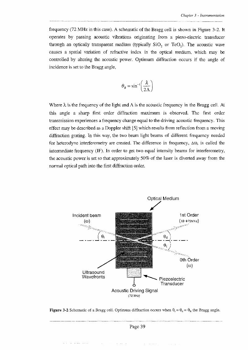
Chapter 3 - Instrumentation
frequency (72 MHz in this case). A schematic of the Bragg cell is shown in Figure 3-2. It
operates by passing acoustic vibrations originating from a piezo-electric transducer
through an optically transparent medium (typically Si02 or Te02) . The acoustic wave
causes a spatial variation of refractive index in the optical medium, which may be
controlled by altering the acoustic power. Optimum diffraction occurs if the angle of
incidence is set to the Bragg angle,
e . -l( It )B =sm 2A
Where A is the frequency of the light and A is the acoustic frequency in the Bragg cell. At
this angle a sharp first order diffraction maximum is observed. The first order
transmission experiences a frequency change equal to the driving acoustic frequency. This
effect may be described as a Doppler shift [5] which results from reflection from a moving
diffraction grating. In this way, the two beam light beams of different frequency needed
for heterodyne interferometry are created. The difference in frequency, ~CO, is called the
intermediate frequency (IF). In order to get two equal intensity beams for interferometry,
the acoustic power is set so that approximately 50% of the laser is diverted away from the
normal optical path into the first diffraction order.
Optical Medium
/
............... PiezoelectricTransducer
Acoustic DriVing Signal(72MHz)
Figure 3-2 Schematic of a Bragg cell. Optimum diffraction occurs when Bj = Bd = BB the Bragg angle.
Page 39

Chapter 3 - Instrumentation
After splitting and frequency shifting by the Bragg cell, the interferometer beams are
guided onto the cantilever using the objective lens. The beams are positioned such that one
beam illuminates the fixed end of the cantilever and the other the free end. With constant
cantilever deflection, a constant phase difference is maintained between the two laser
beams. When the cantilever is contacted to a surface however, the resulting deflection
causes a change in phase difference between the two beams. Such movements are detected
by optically mixing the two reflected beams to produce a signal at the IF. Further electrical
mixing with a reference signal at the IF produces a de signal proportional to the phase of
the original reflected laser beams. Since this phase is determined by the cantilever
deflection, the de signal may be used as a measure of the force of contact of the AFM
cantilever with a surface.
Optical rruxmg after reflection from the cantilever is performed by guiding the
interferometer beams onto a metallic transmission grating. The period of this grating varies
in one dimension and adjusting the position and rotation of the grating makes it possible
to make the two beams coincide. The coincident beams are focused onto a photodiode
where they beat together to produce a signal at the IF. Electrical demodulation using two
orthogonal reference signals produces de signals proportional to the cantilever deflection
(sine and cosine of the optical phase difference). Passive power splitters and double
balanced mixers from Minicircuits'" were used to construct the demodulation circuit. The
photodetector and demodulation electronics were housed in close proximity (in the same
shielded container) to limit electromagnetic interference from the nearby Bragg cell drive
signal.
Mechanical scanning of the probe was implemented using a commercial 3-axis flexure
stage19 with piezoelectric actuators. The piezoelectric actuators operate from 0-150 V and
produce a maximum travel of 13.5 urn, Micrometer screws provide coarse manual
alignment over a 2 mm range. To simplify the alignment of the laser beam to the probe, the
tip was fixed and the specimen scanned. Both tip and specimen were mounted on custom
made holders. Two CCD (charged coupled device) cameras were introduced to help
during the alignment of the laser beams to the cantilever, and the approach of the tip to the
specimen. The optical path of the primary camera was coincident with that of the
interferometer, and a polarising beam splitter cube was used to separate the laser from a
white light source (Figure 3-1). A small proportion of the laser intensity is diverted to the
CCD camera using this set-up, however this was required for the alignment procedure. A
coloured filter was used to attenuate the laser light so as not to saturate the camera. The
IR Minicircuits, PO Box 350166, Brooklyn, New York, USA.19 Elliot Scientific, Gladstone PI, 36-38 Upper Marlborough Rd, St Albans, Herts, UK.
Page 40

Out
In
Feedback Loop
Out
AFM
72MHz
Chapter 3 - Instrumentation
KEY
~ResponseSignals
Figure 3-3 Block diagram of the electronics for the contact mode AFM.
purpose of the second camera (not shown in Figure 3-1) was viewing light transmission
through SNOM apertures, and was thus seldom used for SThM.
3.2 AFM Control Electronics
A schematic diagram of the control electronics for the AFM is shown in Figure 3-3. Most
of the component parts shown predated this project and were designed and built by Dr J.
Weaver. Scanning software was written by a fourth year project studenr". Computer
assembly and software modification were carried out by the author.
The operation of the system mimics in part an older attractive mode AFM system used for
potentiometry. A computer interacts with the AFM through digital to analogue, and
analogue to digital converters (DACs and ADCs respectively). The DACs drive the XY
raster scanning motion, whereas the ADCs collect information from the microscope which
is then plotted on the computer monitor. The feedback loop (single pole integrator) servos
on the signal from the optical interferometer which is proportional to the cantilever
deflection. High voltage (-150 to +150 V) amplifiers convert the computer generated raster
20 Project Student 1994, Department of Electronics and Electrical Engineering, University of Glasgow.
Page 41

Chapter 3 - Instrumentation
motion, and Z height corrections from the feedback loop, into drive signals for the
piezoelectric transducers.
The computer used to drive the microscope was assembled from commercial components.
A fast processor (P150) and hard disk were required because experience of the older
potentiometric AFM had shown that disk write delays limited rapid data acquisition rate.
For attractive mode AFM this was not so critical, since scanning is generally limited by
settling delays of the feedback loop. Contact mode AFM on the other hand, where fast
initial scans are used to give rough positional information, often allows the user to scan at
faster frequencies. Some important elements of the older system were retained however.
The software for scanning was written in 1994 by a final year project student and later
updated by Ashish Midha. An early generation SVGA (8514A) video card was used in
conjunction with a modem SVGA card to provide the user with a twin monitor
environment. To avoid having to configure the software for new hardware, the new
computer was fitted with an identical 8514A card. Few problems were encountered when
fitting this antiquated card to a modem motherboard, however care had to be taken in
selecting a compatible monitor (the pin outs on SVGA cables vary depending on what
degree of auto-detecting is employed). The computer was electrically isolated from the rest
of the microscope in order to break the ground connection between microscope and
computer thus avoiding noise transmission.
The original system used an obsolete DAC/ADC card to drive the microscope (14 bit
DACs, 14 bit ADCs). Although a duplicate card was available, it was not compatible with
the Pentium processor bus speed and so a modem I/O card was used instead to drive
external DACs and ADCs (20 and 16 bit respectively). The new DACs differed from
those on the original DAC/ADC card in that they were serial-in/parallel-out (the original
DACs were parallel-in/parallel-out). A hardware solution to this compatibility problem was
engineered by Dr Weaver involving a series of parallel-in/serial-out shift registers and
some control logic. Subroutines in the Pascal code controlling data streaming to the DACs
were written by the author.
The AFM was tested on completion to check that force regulation was operating
adequately. Topographic scans were acquired using both "blank" Si3N4 Glasgow generic
cantilevers (no defined sensor) and commercial silicon cantilevers from Nanosensors":
The specimen used here was fabricated by Dr J. Weaver using high resolution EBL and
consisted of twin orthogonal metal gratings patterned on a Molybdenum coated Si
substrate. A short (1 urn) period grating was evaporated first using 20 nm Al, then a
21 Nanosensors GmbH, IMO-Building, 1mAmtmann 6, D-35578 Wetzlar-Blankenfeld, Germany.
Page 42

Chapter 3 - Instrumentation
(a) (b)
Figure 3-4 (a) Topographic scan of perpendicular metal gratings on glass using a generic probe. (b) The
same specimen scanned using a sharp commercial silicon tip.
longer (3 urn) period grating was deposited on top using 50 nm AuPd. AFM scans of the
gratings can be seen in Figure 3-4. Reflection of the laser beams from the Glasgow probe
was aided by evaporation of 20 nm AI on the reverse of the cantilever. The scans clearly
show the orthogonal gratings. The difference in contrast between the two images is due to
the superior specimen access afforded by the sharp Si tip. Although high resolution
information is observed using the Glasgow probe, the flat apex tip ("" 1.5x1.5 urn top, 35°
half angle) does not allow the tip to faithfully trace the surface. This is a common artefact
in SPM, resulting in image contrast being governed by the tip shape. The image using the
sharp silicon tip is expected to be a truer representation of the specimen due to improved
specimen access (10 nm tip radius, 15" half angle). This would appear to be the case since
the commercial probe gives stronger contrast (the tip is accessing the trenches between
wires), and more consistent with the evaporated thicknesses (the signal at the thicker
horizontal wires is greater than that at the vertical wires).
Despite the poorer topographic imaging capability of the Glasgow probes compared with a
conventional AFM probe, the strategy of using AFM to position integrated thermal
sensors is still valid. The primary objective of using the force signal is to navigate a
specimen, and thus accurately overlay the simultaneous thermal image. The image in
Figure 3-4 is certainly good enough for this purpose, with topographic features in the
image resulting from structures no more than 1 urn from the sensor.
Page 43

Chapter 3 - Instrumentation
3.3 Thermocouple Circuitry
Special care was taken when designing the methods for physical mounting and electrical
connection of the miniature thermal probes to an external amplifier. Initial efforts to make
electrical connection to thermocouple probes by Dr H. Zhou had shown that the probes
were sensitive to electrostatic discharge (ESD). Calculations estimate that only 3 pJ of
energy would be required to vaporise a typical 1OOx 100x75 nm metal thermocouple
junction (assuming the failure mode is melting, neglecting the possibility of the metals
forming a eutectic, and using 1336 OK as the melting temperature of Au). This corresponds
to the discharge from a 15 mID length of a coaxial cable with lead capacitance 100 pF/m
charged to 15 V (typical situation for a floating input to an opamp). The chosen strategy
therefore involved several features designed to reduce the likelihood of electrical failure of
the probes on contact to external circuitry.
Angled aluminium probe mounts had already been manufactured for use with the contact
mode AFM described earlier. In order to keep connections short, it was decided that the
thermal probes should be mounted on a small printed circuit board (PCB) which would
then be glued onto the aluminium holder. The PCB included copper pads to which the
thermocouple wires could be electrically connected, and featured a single pole low pass
filter (-3 dB breakpoint approximately 30 kHz depending on probe resistance) made from
surface mount resistors and capacitors. The purpose of the filter was to protect the probe
from high frequency signals arising from discharges due to lead capacitance or amplifier
transients. The close proximity (approx. 1 em) of the filter to the thermocouple probe
provided minimum lead capacitance. In most cases, it was expected that the thermocouple
signal would be dynamically detected using a homodyne detector (i.e. the temperature of
the specimen would be modulated). Pre-amplification of the thermocouple signals (of
order 10 !-tV) was employed before input to a lock-in detector so that noise pickup and
impedance mismatches would be minimised. An instrumentation amplifier (Burr Brown'"
INA114) was chosen for its high CMRR and suitable bandwidth (10 kHz at gain = 100).
The amplifier needed to be situated physically close to the probe to decrease lead
capacitance, and so was mounted on a small separate PCB and connected using short (""
15 em) insulated wires. Surface mount components were used on the amplifier board in
order to keep signal paths to a minimum. The buffer amplifier output was connected to the
lock-in amplifier using coaxial cable. A photograph of both the probe mount and amplifier
board are shown in Figure 3-5.
22 Burr Brown, www.burr-brown.com.
Page 44

Chapter 3 - Instrumentation
lcmFigure 3-5 Thermal probe mount with passive filter and amplifier board.
Bonding the thermocouple wires to the circuitry was attempted using a mix of techniques.
Initially ultrasonic bonding with aluminium wires was used, which involved precise
alignment of a metal wedge to the probe. This method was successful, although time
consuming due to the fact that many bond wires failed to stick to either the thermocouple
wires or the copper pads on the PCB. The adhesion problems seemed to be caused by
contamination and the height mismatch between the probe pads and the PCB (equal to the
probe base thickness). Cleaning the PCB in hydrochloric acid prior to bonding increased
the number of good bonds made to the PCB, however cleaning the probe was not possible
due to the fragility of the cantilever. Latterly, silver epoxy was used to secure hanging
bonds, although this technique risked damage to the cantilever. An additional strategy
designed to protect the probe from ESD involved making bonds between the thermocouple
wires to short circuit the sensitive junction. These bonds could be left in place until the
amplifier had been connected and powered up, before being cut using an insulating knife.
In order to improve on the bonding method for electrical connection of the probes, a clip
system was devised (shown in Figure 3-5). Two tiny sharpened beryllium copper strips
were soldered to the existing probe mount PCB, then shaped into angled clips using
tweezers. The sharp ends of the strips were positioned to rest on with the thermocouple
pads on the probe base. A third metal strip was used to raise the two clips while the probe
Page 45

Chapter 3 - Instrumentation
was placed underneath. Annealed beryllium copper has similar mechanical properties to
spring steel and electrical conductivity almost as high as copper. This provides a low
resistance path and means the clips do not deform during the mounting operation. A small
piece of wire (::::: 1 em long) was temporarily used to short the two clips together during
mounting and connection to the rest of the amplifier circuitry. It was cut after the amplifier
had been powered up using an insulating knife.
[1] G. Meyer and N. M. Amer, "Novel optical approach to atomic force microscopy," AppliedPhysics Letters, vol. 53, pp. 1045-1047, 1988.
[2] S. Alexander, L. Hellemans, O. Marti, J. Schneir, V. Elings, P. K. Hansma, M. Longmire, and1. Gurley, "An atomic-resolution atomic-force microscope implemented using an optical-lever,"Journal Of Applied Physics, vol. 65, pp. 164-167, 1989.
[3] Y. Martin, C. C. Williams, and H. K. Wickramasinghe, "Atomic force microscope forcemapping and profiling on a sub 100-a scale," Journal Of Applied Physics, vol. 61, pp. 47234729, 1987.
[4] Y. Martin and H. K. Wickramasinghe, "Magnetic imaging by force microscopy with 1000-aresolution," Applied Physics Letters, vol. 50, pp. 1455-1457, 1987.
[5] H. Cummins, N. Knable, L. Gampel, and Y. Yeh, "Frequency shifts in light diffracted byultasonic waves in liquid media.,' Applied Physics Letters, vol. 2, pp. 62-64, 1963.
Page 46

Chapter 4 - Thermocouple Probes
4 Thermocouple Probes
4.1 Thermoelectricity
A thermocouple thermometer is an electrical circuit consisting of at least two dissimilar
conducting elements. Three related thermoelectric effects govern the operation of a
thermocouple. If a temperature gradient exists between the junctions of two dissimilar
conducting elements (see Figure 4-1(a», then an emf is produced which may drive current
round a closed loop. This phenomenon is called the Seebeck effect, named after Thomas
Johann Seebeck to whom the discovery is attributed. The absolute Seebeck coefficient
(ASC), or absolute thermoelectric power, (S) of an individual element in a closed circuit
may be described asT
S(T) = f (jdtaT
Where a is the Thomson coefficient of the material and T is absolute temperature. The
algebraic sum of the ASCs of individual thermoelectric elements in a circuit produces the
relative Seebeck coefficient (RSC) of the thermocouple. The open circuit RSC of a
thermocouple is given by (see over)
Heat
\tl Joule Heat
B \tlA B T1 T2
It\It\ Thomson Heat
Heat
(a) (b) (c)
Figure 4-1 (a) If materials A and B are different conductors then the Seebeck effect produces an emf that
drives a current i proportional to the temperature difference of the junctions. (b) If A and B are dissimilar
conductors, and a current i is driven round the closed circuit, Peltier heating will occur at one junction and
Peltier cooling at the other. Reversing the direction of the current flow changes the direction of energy
flow at the junctions. (c) Thomson heat is the reversible heat absorbed or evolved (dependent on direction
of current) when a current passes through a single conductor subject to a temperature gradient. This is
additional to any resistive joule heating which is not reversible.
Page 47

Chapter 4 - Thermocouple Probes
dEAB =S -SdT A B
Where EAB is the emf produced by a thermocouple made from materials A and B. SA and SB
are the ASC's (normally measured in llVrC) of the individual conductors. The emf in a
thermoelectric element subject to a temperature gradient is caused by a voltage which
retards the thermal diffusion of electrons from hot to cold areas. In addition to this, the
Fermi level of element varies with temperature which produces a second voltage
contribution. This combination of voltages produces the driving emf for thermocouple
circuits. A complete quantum mechanical analysis of the origin of these effects is beyond
the scope of this text but is described in full elsewhere [1-3].
The Peltier heat was named after Jean Charles Peltier who discovered the effect in 1834.
He observed that passing a current across the junction of two dissimilar materials resulted
in heating or cooling at the junction depending on the direction of current flow. In a circuit
consisting of two dissimilar conductors as in Figure 4-1(b), energy is liberated at one
junction and, if the circuit is isothermal, the same amount of energy is absorbed at the
other. The Peltier coefficient PAB' with current passing from material A to B, may be
expressed simply as
Where T is the absolute temperature of the junction and (}A and (}B are the Thomson
coefficients of the two conductors A and B.
Finally, the Thomson effect is the reversible heat produced when a current is passed
through a conductor which is subject to a temperature gradient. This phenomenon was
proposed by William Thomson (later Lord Kelvin) to complete a thermodynamic theory
of thermoelectricity [4], and later measured experimentally for a variety of materials [5].
Reversible heat is energy that is liberated or absorbed depending on direction of current
flow. This heat is additional to the Joule heat which is always liberated. The heat energy Q
produced per unit volume per unit time in the conducting element in Figure 4-1(c) is given
by
Q .J + .dT=rp-O]
dx
Where j is the current density, p is the electrical resistivity of the thermoelement, and o is
the Thomson coefficient. The first term is the Joule heating, but the second term (the
Page 48

Chapter 4 - Thermocouple Probes
Thomson heat) may be positive or negative depending on the direction of the current flow
with respect to the temperature gradient.
Both the Thomson and Peltier heats are closed circuit effects (they require current flow)
and may produce errors in thermoelectric thermometry. Most practical thermocouple
circuits however are usually operated open loop or with negligible current flow, and so
these effects may be ignored. Errors may also occur with the introduction of electrical
leads for the purpose of measurement [6, 7]. These may be avoided by maintaining the
junctions of the thermocouple arms and the measurement leads at a reference temperature.
The measured signal is then proportional to the difference in temperature between the
measuring and reference thermocouples.
4.2 Material System
Thermocouple selection for the development of the Glasgow SThM probes was inherited
from initial investigations by A. Midha, 1. Weaver, and H. Zhou [8] and consisted of a
AulPd thermocouple with a thin NiCr intermediate layer for adhesion purposes. This
decision was based on a number of practical requirements relating to fabrication and
performance. It had been decided that initially the thermoelements be limited to those
metals that were available for deposition in the Plassys MEB evaporator, namely Ni, NiCr,
Ge, Ti, Au, Pd. The reason for this was that there was easy access to this evaporator in a
clean environment which made for quick, reliable film deposition. In addition, the
thickness of these metals could be controlled to ± I nm (important for lift off
development). Further limitations were that the metals should be compatible with
potassium hydroxide etching, and the lift off process used for definition of the
thermocouple wires. The noble metals Au and Pd were chosen because they have a
reasonable RSC (12 /lVrC at 300K [1]), are unreactive in potassium hydroxide, are
thermoelectrically stable up to lOOO°C in air [9] and do not readily form oxide coatings in
air. The last requirement here is important for thin film thermocouples since the
thermocouple interface is necessarily exposed to air between electrode deposition levels.
Metals which would have produced a higher RSC like Ni and Ni o.6Cr0.4 (assuming similar
properties to Nickel/Chromel thermocouples), were rejected because they both form
surface oxide layers in air which could potentially degrade the electrical continuity of the
thermocouple.
The thicknesses of the metals were chosen to provide a low resistance thermocouple so
that the emf drop across the voltage measurement circuitry would be maximised.
Lithographic considerations however dictate that the metal thickness be of the order of the
minimum desired feature size, and one metal be thicker than the other to ensure continuity
Page 49

Chapter 4 - Thermocouple Probes
Figure 4-2 Test structure showing two separate wires intersecting at the apex a micromachined pyramid
(courtesy of H. Zhou).
at the junction. Experiences of A. Midha had shown that both Au and Pd did not adhere
satisfactorily to silicon nitride [8], and so a KOH compatible adhesion layer consisting 5
nm Nio.6CrOA was required for each arm of the thermocouple. This layer was not expected
to change the behaviour of the thermocouple since at such thicknesses the layer is not
continuous, and resistive compared to the Au and Pd electrodes. Having satisfied the above
criteria, test thermocouples using metal thicknesses of 20 nm Au and 45 nm Pd (excluding
adhesion layers) were demonstrated by A. Midha and Dr H. Zhou, and so these values
were retained for initial attempts at making thermocouples on probe tips.
4.3 Cross Thermocouples
The cross thermocouple probes were developed jointly with Dr Haiping Zhou. The
principle was to have two dissimilar wires (Au and Pd) intersect over the apex of one of
the generic probes. This automatically made sensor definition a two step process.
Alignment between these two levels was important in so far as the sensor was to be
positioned on the flat apex of the pyramid, but by its nature the cross thermocouple would
yield a junction in every instance of misalignment.
Figure 4-2 shows an early pyramid test structure fabricated by Dr Zhou. These were
constructed on substrates without the back processing normally found on the real device
substrates. A cross thermocouple has been written at the pyramid apex, and the overlap of
the wires that form the thermocouple junction can be clearly seen. The bottom wire is a
bilayer of 5 nm Nio.6CrOA and 20 nm Au and the top wire is 5 nm Nio.6CrOA and 45 nm
Pd. Probing for continuity using a de probe station yielded a value for junction resistance
of around 500 Ohms. Temperature dependence of the devices was then investigated by
measuring their voltage response when pumped with an argon laser. The bulk materials
Page 50

Chapter 4 - Thermocouple Probes
c 5HzcFrequency
I- ~Thermal
I--Optical
i
.l\,A ~!IMAt ~""
~.Jilt " '~'I . r'
~\ ","'" ''''''
- ).t1Z co co +
-20
o
rr-.U
~<:».---< -40coSo.......ir:
-60
Figure 4-3 Spectral trace of a thermocouple on a pyramid apex when
heated by a mechanically chopped laser (courtesy of 1. Weaver).
predicted a junction Seebeck coefficient of 12 ~Vrc. It was shown that the actual value for
such thin film thermocouples is in fact similar to within a factor of two, (error arising from
the uncertainty of the laser spot size). Examination of the close-in noise spectra of the
laser and thermal response of the thermocouple (Figure 4-3) shows little difference
demonstrating that the 1/f noise in the sensor is less than that of the laser [10].
Dr Zhou continued to make cross thermocouples on back etched substrates with silicon
Figure 4-4 CAD pattern for device layers of the cross thermocouple probe.
Page 51

Chapter 4 - Thermocouple Probes
nitride cantilevers. The CAD patterns for the sensor layers of the cross thermocouple
probe are shown in Figure 4-4. An extra level was added after the sensor definition which
included thick Au pads for bonding to the thermocouple wires, and a Au mirror on the
cantilever to reflect the force sensing laser beams. The contact between the Pd wire and the
Au pads forms a second thermocouple which has a junction area of several thousand
square microns. The thermovoltage from the probe is proportional to the temperature
difference between the thermocouple at the tip apex and this second "reference"
thermocouple. By positioning this thermocouple on the probe base, its temperature may be
approximated to that of the silicon substrate. This may assumed to be room temperature in
most cases however care must be taken to account for situations where the temperature of
the reference thermocouple may be changed (e.g. thermally radiative specimens).
After optimising the electron exposure, Dr Zhou fabricated a small number of operational
thermocouple probes. Yields of order 10% per wafer were observed. Figure 4-5 shows a
completed pre-release cross thermocouple probe. The minimum wire widths, and hence
thermocouple junction sizes were 70 nm in this case. Tests after release showed the
continuous thermocouples to have electrical resistances of approximately 1 k,Q. The
probes were cleaved and attempts were made to use ultrasonic bonding to contact to the
gold pads. Problems with contamination on the pad surface, which resulted in poor
adhesion of the bonded wires, prompted attempts to use silver loaded epoxy to make the
electrical connections. Unfortunately many probes became open circuit after the bonding
process. It was suggested that this was due to electrostatic discharges (ESD) vaporising
the thermocouple junctions. None of the cross thermocouple probes were scanned due to
electrical failure on connection to the external measurement circuit.
A later demonstration by the author of the lithographic limit of patterning these wires over
the flat topped micromachined pyramids is shown in Figure 4-6. A semi-processed
Figure 4-5 Plan view of AuJPd thermocouple situated at the apex of a pre release micromachined tip
(courtesy of H, Zhou).
Page 52

Chapter 4 - Thermocouple Probes
Figure 4-6 Approaching the resolution limit of a single wire on the apex of a micromachined pyramid.
thermocouple (consisting of only the Au thermocouple arm) was accidentally broken
during processing, and this allowed some of the wires to be scribed and put in a Hitachi
S900 (small specimen, high resolution electron microscope). The original wafer had been
an exposure test and therefore a variety of thicknesses of wires were found. Typically the
wires were 30-50 nm wide at their narrowest point. Wires with a width of 25 nm were also
demonstrated on another wafer and appeared continuous when imaged using the lower
resolution S800 SEM. A selection of the pre-release 25 nm thermocouples were probed
using the de probe station, but all became open circuit after conducting momentarily. One
reason for this could be that too large a current was used (100 flA compliance) and the
device was breaking down due to electrical overstress. Alternatively ESD from the probe
needles may have caused the failures, however care had been taken to short the two needles
together before measurements were attempted. After the release etch, the rest of the 25 nm
thermocouples appeared to be open circuit after examination by SEM. The wires appeared
to have detached from the cantilever surface during the etch. This poor adhesion may have
been caused by contamination under the wires.
A second generation design for the cross thermocouple probes involved larger pads to
facilitate bonding with silver loaded epoxy. Figure 4-8 shows the arrangement of these
pads on the substrate. The Au wire is joined at both ends by a single Au pad whereas the
Pd wire has a Au pad at each end. This arrangement increases the area of Au for external
connection purposes. The two pads attached to the Pd wires would have been made into a
single pad were it possible.
Page 53

Chapter 4 - Thermocouple Probes
Figure 4-8 Pad arrangement for "cross" thermocouples. Note that two of the pads
are shorted together. The blocks of six local alignment markers are clearly visible.
4.4 Triple Thermocouples
Several potential advantages are offered by incorporating more than one thermal sensor on
an AFM probe. One possible application is the creation of a parallel thermal scanner
which could scan multiple sensors simultaneously and thus increase throughput of the
measurement system. For example, benefits in the form of increased data transfer rates to
techniques like AFM storage [11] may realisable. Investigations have been made using
multiple lever instruments [12], but not yet with multiple sensors on a single cantilever.
Another possible utility for multiple thermal sensor probes is the investigation of the
parasitic tip contact changes which cause artefacts in thermal AFM imaging. By measuring
the temperature at several different sites on the probe tip, it may be possible to determine
Figure 4-7 CAD patterns for the device layer of the triple thermocouple probe (Blue=Pd, Yellow=Au).
Page 54

Chapter 4 - Thermocouple Probes
what part of the tip in contact and the quality of the contact. The ability to subsequently
correct a thermal image by compensating for tip contact variations would be extremely
valuable, especially with highly topographic specimens. A final benefit of making multiple
sensors is that the yield of operable probes increases. Multiple sensors means that there
are multiple chances of making at least one good sensor per probe. Conversely of course
this means that the chance of all sensors succeeding on a single probe decreases as
sensors are added, and so multiple sensor probes are expected to have relatively low yield.
In order to demonstrate the practicality of multiple sensor probes, it was decided to make
triple thermocouple probes. It has been shown that a single thermocouple can be made
using a variety of methods [13-16], and although twin thermocouple probes have not yet
been fabricated it was thought that triple thermocouples would more readily show an
ability to extend to "n" thermocouple probes. For example, twin near field optical sensors
have been demonstrated [17], however the technique does not readily extend to more
complex arrangements because the apertures are only loosely controlled through timed
etched and not patterned lithographically.
The layout of the three thermocouples consisted of a common gold arm and three
bisecting Pd arms (Figure 4-7). Ideally each thermocouple would be completely separate
from the others (in order to reduce electrical crosstalk and increase thermal resistance
among the sensors), but it was felt that packing six leads and six pads onto a single probe
;-
:
1
I
=J-
I
11[ '<
I········
(a) (b)
EB Pixels in CAD
Actual Exposure
Figure 4-9 (a) By defining a single pixel wire and using the exposure to control the shape it was found
that the arrowed regions were susceptible to open circuit. (b) By using multiple pixels to form the
constriction, and smoothing the edges, increases in successful wires were observed, but at the expense of
flexibility and minimum wire width.
Page 55

Chapter 4 - Thermocouple Probes
was impractical for a first attempt. New problems were already anticipated with writing a
long narrow constriction in the Au wire, and multiple high resolution wires in the Pd layer.
Some novel design changes were implemented to combat these potential problems. During
the fabrication of the cross thermocouples, it was discovered that the rounding of sharp
edges aided lift off considerably. Applying this to the high resolution features, the tapers
in the wires (where the thermocouples are formed) were smoothed. The result was an
increase in well lifted off features, and a decrease in destructive open circuits at the tapered
region. A second design change saw a move away from defining the high resolution
features using dose variation. Originally the taper in each of the cross thermocouple wires
had been made by drawing a single pixel (5 nm) wire in the CAD package (see Figure 4
9(a)), and varying the dose of electron exposure to define the width of the wire. This was
felt to be sub-optimal however since the resulting exposure profile of the wire resembles
that of a single Gaussian giving poor edge definition. Wide wires had also been observed
to leave adjoining features over-exposed. By defining the wire in CAD to be
approximately the desired width (about 30% less to account for some feature growth) and
then exposing at a lower dose, a "plateau" exposure profile is created (Figure 4-9(b)).
One advantage of this is that feature edges are better defined, however it also means that
feature width must be more or less predetermined in the software and so some flexibility is
lost.
Another development to aid the lift off, of the Pd layer in particular, was the lengthening of
the metal wires so that each bisects the whole pyramid. This is a ploy to facilitate the
tearing nature of lift off (see Section 2.5). Small, isolated portions of material are most
Figure 4-10 First pre-release triple thermocouple probe. Note how the wires continue over the pyramid
past the junction to aid lift-off. Close up of the triple thermcouple junctions. Note that the middle wire
appears discontinuous, however this discontinuity occurs on the other side of the gold wire from the pads
and so does not affect the operation of the probe.
Page 56

Chapter 4 - Thermocouple Probes
likely to fail during lift off, however lengthening the wires over the pyramid improves the
chances of the bulk of the surplus material pulling away the small areas at the tip apex. An
analogy for this would be peeling adhesive tape (shaped like the thermocouple wires) from
a surface. Tears, which could propagate and cause the tape not to peel off in one piece, are
most likely to originate at sharp comers. By smoothing these comers, tearing can be
reduced and successful removal of the tape (lift off) increased.
The triple thermocouples were fabricated after exposure tests were conducted to find the
optimum dose for the definition of the high resolution features (z 3500 Czcrrr), Lifting off
the long Au wire proved to be non-trivial, since discontinuities were often apparent along
the narrowest part of the wire. Changing the wire in CAD from single to multiple pixels, as
described earlier, improved continuity significantly while allowing neighbouring features
to be well exposed. This increased the yield of good Au wires from around 10% to 80%
with wire widths of approximately 100 nm. Early attempts at fabricating the three Pd wires
also tended to fail but in this case because surplus material was remaining at the tip apex
which short circuited the wires together. Rounding of sharp features improved the quality
of the lift off for the reasons described earlier, and again produced yields of around 80%.
A finished probe is shown in Figure 4-10. From four quarter wafers, typically 50% of
completed probes had all three thermocouples electrically continuous. The rest had single
("" 20%) or double ("" 20%) thermocouples, leaving only a small proportion ("" 10%)
having failed completely. Resistances of the thermocouples were in general matched to
within 50 Q. The calculated difference in resistance due to a thermocouple being situated
at one or other end of the long Au wire is 30 Q, and in general the resistances
corresponded to thermocouple position. This was not always true however due to the other
factors affecting the resistance such as imperfections in wire shape, and contamination at
the junction.
Beyond electrical continuity testing, the thermal dependency of the thermocouples was
demonstrated by mounting the thermal probes in the Glasgow AFM (see Chapter 3) and
manually bringing a commercial Peltier cell23 into close proximity (see Figure 4-11). A
Peltier cell is a thermopile sandwiched between two plates made from an electrically
resistive, but thermally conductive materiaL The geometry is optimised such that when a
current is passed one side of the device experiences Peltier cooling, and the other Peltier
heating. For this particular cell, a current of 1.2 A at a voltage of 0.48 V produces a heat
rise on the hot side of +67 "C, The middle thermocouple of a fully operational triple
thermocouple was connected to the pre-amplifier circuitry the using the clamp method (see
Section 3.3). The other two thermocouples were left open circuit. The thermocouple
23 RS Electronics Peltier Mini Module
Page 57

Chapter 4 - Thermocouple Probes
resistance was 800 Q. The Peltier cell was positioned using micrometer screws such that it
was close ("" 30 IJID), but not touching, the triple thermocouple probe. The bottom of the
cell was aligned to the probe tip so that minimum heat from the cell impinged on the
second "reference" thermocouple at the Au-pad/Pd junction. The graph shown in Figure
4-11 shows the variation in thermocouple voltage with increasing Peltier current
(increasing temperature). A maximum Peltier current of 0.5 A gave a thermocouple voltage
of 6.5 mY. The noise level after xlOO amplification was 0.25 mY. Assuming the
thermocouple has bulk thermoelectric properties (12 IlvrC) this corresponds to a
temperature difference between the "reference" and measuring thermocouples of
approximately 5.5 "C. This figure is reasonable since the hot side of the Peltier plate may
be assumed to rise by around 15°C at 0.5 A. In addition to this, the probe tip was not well
thermalised to the plate since it was not in contact, and the signal would have been further
diminished by additional heating of the "reference" thermocouple by the Peltier plate.
Another test was made to determine the matching of the three thermocouples. The probe
was optically pumped by focusing a laser (Ar+, 5 mW, 514 nm) on the thermocouples.
The laser was focused onto the mirror situated on the cantilever, thus heating the
7 ~ .
I> •Heat
0.40.30.20.1
Thermoelectric Response of Triple Thermocouple
PeltierCell
Pellier Current (A)
--+- Tnormccouple Vollage (xl00)
Figure 4 -11 Graph showing the temperature dependence of one of the thermocouples on a completed
triple thermocouple probe.
Page 58

Chapter 4 - Thermocouple Probes
thermocouples uniformly. The laser was modulated at 400 Hz and detected using a lock in
amplifier. The voltage response was recorded for each of the three thermocouples yielding
values of 198 !lV, 198 !lV and 202 !lV (±1 !lV). This corresponds to a matching of no
worse than 3%. It is interesting to note that although the resistances of the thermocouples
varied on average by about 6%, due to pattern imperfections, junction sizes and quality of
contact at the junctions, the Seebeck coefficient varied by significantly less. This is
consistent with the behaviour of bulk thermocouples. The 3% mismatch may arise from
factors such as non-uniform heating due to roughness, asymmetry of the wires on the
cantilever, local purity variations in the electrode metals, or mechanical stress.
Further experiments involving the triple thermocouple probes were attempted, including
scanning a semiconductor laser diode facet. Unfortunately out of contact scans were
dominated by heating from the laser light and not the facet itself. When contacted to the
specimen surface, problems with crashing the probe over the edge of the facet and
contamination of the tip with conducting adhesive from the specimen were experienced.
No meaningful data was obtained, however it was encouraging that probe failure was
observed to be due to gross mechanical impacts rather than sensor wear or electrostatic
discharge.
[1] Thermocouples Theory and Properties: CRC Press Inc, 1991.
[2] W. F. Roeser, "Thermoelectric thermometry," Journal of Applied Physics, vol. 11, pp. 388-407,1940.
[3] Thermoelectricity: an introduction to the principles. New York: John Wiley and Sons, Inc.,1962.
[4] W. Thomson, "Communication on a mechanical theory of thermo-electric currents," Proc. Roy.Soc. Edin., 1851.
[5] W. Thomson, "Account of Researches in Thermo-electricity," Proc. Roy. Soc. Lon., vol. VII,1854.
[6] R. P. Reed, "Thermoelectric thermometry: a functional model," in Temperature, its measurementand control in science and industry. New York: American Institute of Physics, 1982, pp. 915922.
[7] R. P. Reed, "Ya Cant Calibrate a Thermocouple Junction .1. Why Not," Measurements &Control, pp. 137-145, 1996.
[8] A. Midha, "Batch-fabrication of novel nanoprobes for SPM," in Electronics & ElectricalEngineering. Glasgow: University of Glasgow, submission due 1999.
[9] Y. G. Kim, K. S. Gam, and C. Rhee, "1000 H Stability Test Of the Au/Pd Thermocouple At1000-Degrees-C," Metrologia, vol. 33, pp. 337-339, 1996.
Page 59

Chapter 4 - Thermocouple Probes
[10] H. Zhou, A. Midha, G. Mills, S. Thoms, S. K. Murad, and J. M. R. Weaver, "Generic scannedprobe microscope sensors by combined micromachining and electron-beam lithography," JournalOf Vacuum Science & Technology B, vol. 16, pp. 54-58,1998.
[11] B. W. Chui, T. D. Stowe, T. W. Kenny, H. J. Mamin, B. D. Terris, and D. Rugar, "Lowstiffness silicon cantilevers for thermal writing and piezoresistive readback with the atomic forcemicroscope," Applied Physics Letters, vol. 69, pp. 2767-2769, 1996.
[12] S. C. Minne, S. R. Manalis, and C. F. Quate, "Parallel atomic force microscopy usingcantilevers with integrated piezoresistive sensors and integrated piezoelectric actuators," AppliedPhysics Letters, vol. 67, pp. 3918-3920, 1995.
[13] Y. Suzuki, "Novel microcantilever for scanning thermal imaging microscopy," Japanese JournalOf Applied Physics Part 2-Letters, vol. 35, pp. L 352-L 354, 1996.
[14] M. Stopka, E. Oesterschulze, J. Schulte, and R. Kassing, "Photothermal scanning near-fieldmicroscopy," Materials Science and Engineering B-Solid State Materials For AdvancedTechnology, vol. 24, pp. 226-228, 1994.
[15] J. Lai, M. Chandrachood, A. Majumdar, and J. P. Carrejo, "Thermal detection of device failureby atomic-force microscopy," Ieee Electron Device Letters, vol. 16, pp. 312-315, 1995.
[16] K. Luo, Z. Shi, J. Varesi, and A. Majumdar, "Sensor nanofabrication, performance, andconduction mechanisms in scanning thermal microscopy," Journal Of Vacuum Science &Technology B, vol. 15, pp. 349-360, 1997.
[17] E. Oesterschulze, O. Rudow, C. Mihalcea, W. Scholz, and S. Werner, "Cantilever probes forSNOM applications with single and double aperture tips," Ultramicroscopy, vol. 71, pp. 85-92,1998.
Page 60

Chapter 5 - Improved Access Thermocouples
5 Improved Access Thermocouples
5.1 Motivation
A great deal of research during this project was involved with developing a thermal probe
that offered better specimen access than the generic pyramid probes with flat apices. The
blunt pyramidal tips are suitable for relatively flat specimens, but for highly topographic
specimens the ability of the probe to faithfully trace the surface is compromised. Poor
specimen access is a common cause of artefacts in conventional AFM [1] and has also
been shown to cause spurious features in thermal imaging [2]. In general artefacts may be
reduced with any given specimen by reducing the (microscopic) tip radius and the
(macroscopic) opening angle of the probe.
The measurement of specimens from the semiconductor industry was of particular interest
due to the Motorola sponsorship of the project. Passivated integrated circuits typically
have densely packed protrusions several microns high, and so tip access is of great
importance if SPM analysis is desired. Specimen preparation techniques which remove
passivation by chemical means or planarise the specimen by mechanical polishing are
common, however they can cause degradation of the original thermal properties of the
specimen. To avoid this, methods for making a probe with good access were devised
which involved reducing both the opening angle and tip radius of the probe (defined on the
generic probe by the pyramid shape and the flat apex respectively).
5.2 Fabrication Development
An early idea to make an improved access probe relied on making the ends of two sharp
wires overlap on the side of one of our generic pyramids. If the material supporting the
wires could somehow be selectively removed by further processing, the free metal
thermocouple would form a lithographically defined asperity which could then be scanned.
The opening angle would also be improved if the angle between the two wires was less
than the opening angle of the pyramid. In order to test feasibility of aligning and
transferring EBL patterns where the critical features were situated on a sloped surface,
preliminary tests were carried out. Custom made substrates with etched pyramid tips, but
without the back etched membranes, were fabricated. Topographic EBL markers similar to
those used with the generic substrate were positioned a known distance away from the
pyramids. Using this scheme, two separate lithographic levels were written to form wires
with coincident sharp tips (Figure 5-1).
Page 61

(a)
Chapter 5 - Improved Access Thermocouples
(b)
Figure 5-1 Side thermocouple test specimens.
Several problems were encountered during the testing. Firstly, lift-off of the wire tips
proved to be extremely difficult and often resulted in catastrophic failure. The most
common failure mode was a metal "cap" remaining over the pyramid apex. This had also
been observed with the conventional flat apex thermocouples, but had been improved by
applying several short bursts of ultrasonic agitation. Unfortunately ultrasonic lift off did
not significantly improve matters when applied to these test structures. It appeared that
although the resist under the metal was dissolving (which should have freed the metal to
float off into the acetone), the metal was failing to release and sticking back down to the
pyramid (Figure 5-2). Once settled back on the substrate, the metal held firm against
attempts to dislodge it (presumably due to capillary forces). In order to free the metal caps,
the patterns were rewritten, but this time a lift-off aid in the form off a cross was patterned
(a) (b)
Figure 5-2 Sharp wire test structures patterned on the side of pyramids. Left: Failed lift off due
to capping. Right: Successful lift off with a cross shaped lift off aid at the apex of the pyramid.
Page 62

Chapter 5 - Improved Access Thermocouples
at the top of the pyramid (see Section 2.5). The cross was separate from the thermocouple
wires, but introduced extra lines along which the metal could tear. In conjunction with
ultrasonic agitation, this almost completely solved the lift off problem. The size and shape
of the lift off aid was varied to maximise both removal of the metal cap, and the lift off
quality round the tip. Figure 5-2 shows a typical cross structure and the resulting
improvement in lift off.
A second problem arose in writing EEL defined wires with sharp points. Initial wires had
tip radii of 150 nm and greater, depending on taper angle, which was far greater than
intended. The wires were defined in software to terminate in a single 5 nm pixel, and were
written with a 12 nm spot size. Practical EEL using the Leica machine can in general
produce minimum feature sizes of 25 nm, and on sloped surfaces with imperfect focus
conditions features somewhere in the region 50 nm were expected. Varying the electron
exposure and development did not improve the tip sharpness. Features either appeared
over exposed (over developed) and rounded, or under exposed (under developed) and
rounded. There appeared to be very precise conditions at which ideal exposure and
development would cause sharp tips. Instead of further efforts to identify the exact
exposure conditions, it was decided to try and desensitise the pattern to exposure dose.
This was achieved by distorting the shape of the tip in software so that development would
give the desired shape. A single pixel protrusion from the tip was added to the written
pattern. The length of this additional feature was varied and it was discovered that using a
length of 75-125 nm (dependent on taper angle) yielded sub 50 nm diameter tip sharpness
under normal exposure and development conditions. This may be thought of as an
exposure compensation technique, similar to proximity correction [3], but for isolated
features instead of densely packed features.
A final problem was encountered in the alignment of features. There were four main
components to the alignment:
• Aligning the marker to the pyramidal tip.
• Aligning the critical features to the pyramidal tip.
• Aligning the different matrices (in the same lithographic level) to each other.
• Aligning different levels accurately to each other.
The first two are related because alignment of a feature to the tip depends critically on how
well the position of the marker is known with respect to the pyramid. Local markers and
pyramids are written on a three inch wafer in the same EEL leveL The job takes several
hours to write and in that time, despite periodic corrections, stage drift can result in
misalignments of several hundred nanometres. To avoid these drift errors a scheme was
Page 63

Chapter 5 - Improved Access Thermocouples
devised by A. Midha which involved quickly writing one matrix containing the outlines of
the markers and pyramids, then a second longer matrix which filled in the remaining areas.
By this method the edges of the features were well placed, and any drift errors when
writing the bulk of the pattern were made redundant.
Aligning different matrices to each other was necessary because different spot sizes and
focus conditions were needed to write large areas in a sensible time. Exactly where the
marker was found however seemed to depend on the spot size, electron energy and focus
conditions of the EBL machine and this could in turn cause gaps in the exposed pattern.
Creating an overlapping area common to two adjoining matrices was common practice for
planar lithography in order to compensate for small drift errors (z 50 nm). In this case
however, random errors in the range 250-500 nm were observed with the three
dimensional substrates, especially with the lower resolution matrices. By increasing the
size of the overlapping areas it was possible to maintain the continuity of individual
features, but at the expense of good definition. The reason for these particular
misalignment errors remains unclear. The last and most critical aspect to the alignment of
the coincident thermocouple wires was aligning the two lithographic levels which defined
the thermocouple arms to each other. Care was taken to use the same alignment marker,
spot size, focus conditions and electron energy for each level since errors here would
determine the size and shape of the thermocouple junction. Despite these measures errors
of several hundred nanometres were observed. Some well aligned thermocouples were
fabricated, however these were attributed to the random nature of the errors rather than
genuine cases of good alignment. More often, the misalignments would cause the wires
miss each other altogether creating an open circuit, or cross over further down the length
of the wires creating double tips. Figure 5-3 shows the different tip profiles caused by
(a)
1J1m
(b) (c)
Figure 5-3 (a) Two wires well aligned to each other. (b) Misalignment causing an open circuit. (c)
Misalignment causing a double tip.
Page 64

Chapter 5 - Improved Access Thermocouples
misalignment of the two thermocouple layers. Without intimate knowledge of the
procedure used by the electron beam-writer to determine the position of the markers, it
proved difficult to determine the cause of the alignment errors. By trial and improvement
however it was possible to limit the misalignments by implementing the following
measures:
• Use 100 kV not 50 kV electron beam since observed misalignments were greater
between matrices with 50 kv. The greater depth of focus provided by 100 kV resulted
in less feature growth when out of focus.
• Use local alignment markers instead of global markers (reduces any errors which are a
fraction of the distance from marker to pyramid).
• Disable the automatic drift calibration (an error in the software causes the machine to
align to a site then compensate for drift which has already been eliminated).
• When fractionating patterns, human error in positioning matrices can result in
misleading failures. Automatic centring of patterns is possible using the CATS
software and is recommended.
• Use the same marker for critical alignment levels.
• Use the "cross method" which involves using a cross structure remote from the real
marker for coarse operator alignment. Without this, the first marker set is heavily
exposed and may be degraded for the subsequent levels.
The process of aligning the ends of two metal wires to each other was transferred to the
generic substrates. Figure 5-4 shows a pre-release probe with a completed thermocouple.
Despite the improvement in alignment provided by the improved operating procedure,
errors of 250 nm were still occurring on a regular basis. Because of this, and the perceived
difficulty of subsequently removing the underlying silicon nitride to free the thermocouple,
a new probe design that used a degree of self alignment was developed.
Figure 5-4 Two sharp tipped coincident wires on a generic substrate.
Page 65

Chapter 5 - Improved Access Thermocouples
-:Gold
Figure 5-5 Schematic of the side self aligned thermocouple structure.
5.3 "Side" Thermocouple Probes
The principle feature of the new design, called the improved access thermocouple probe
(or "side" thermocouple), was a change in the shape of the silicon nitride cantilever.
Figure 5-5 shows a graphic representation of the new design. Instead of a cantilever that
encompasses the pyramid, the silicon nitride is shaped into a sharp triangular tip
positioned on the side of the generic silicon pyramid. Subsequent thermocouple wire
levels are written such that they coincided at the sharp end of the triangular cantilever to
form a junction, but also overlap the cantilever onto the sacrificial silicon membrane.
Removal of the silicon membrane in the final level causes the removal any part of the
thermocouple wires not on the triangular cantilever. This can be thought of as self
alignment in one dimension. Figure 5-6 shows SEM micrographs of the new cantilever
shape, and the deposition of the metal wires to form the thermocouple. Identical wire
thicknesses (5 nm NiCr/20 nm Au and 5 nm NiCr/45 nm Pd) to those used for the flat
apex devices were deposited for the "side" thermocouple. Normally the cantilever was
transferred into a Cr RIB mask by wet chemical etching. This scheme however was not
compatible with the definition of sharp features because wet etches are isotropic and so
etch laterally as well as vertically, causing sharp comers to be degraded. This was known
to be the case with the conventional cantilevers, but of little consequence because the edges
of the cantilever were not critical features. With the triangular "side" cantilever however
the definition of the cantilever determines the tip profile and width of the thermocouple
Page 66

Chapter 5 - Improved Access Thermocouples
(a) (b) (c)
Figure 5-6 "Side" thermocouple probe. (a) Dry etch mask for the cantilever. (b) Au thermocouple
wire overlapping the dry etched cantilever. (c) Au and Pd wires forming the thermocouple junction.
wires. It was necessary therefore to use a two step process to pattern the triangular
cantilever. An initial lithographic level and wet etch of the original sputtered Cr layer
broadly defined the cantilever shape up to the base of the pyramid. A second overlapping,
high resolution, EEL level was lifted off in 100 nm of Nio.6Cr0.4 to define the critical
triangular end of the cantilever. Using the exposure compensation strategy outlined in
section 5.2, well defined tip profiles were achieved in the RIB mask materiaL The mask did
degrade slightly during RIB etching due to imperfect selectivity between NiCr and silicon
nitride, which resulted in tip radii increasing from below 50 nm to around 100 nm.
Although the problems of producing a free space thin film thermocouple and
misalignment causing double tips had been addressed by the "side" design, the problem
of misalignment between EEL levels distorting the shape of the thermocouple junction was
still evident. In addition to this, the nature of the physical contact between thermocouple
and specimen had been changed. With thermocouples fabricated on the flat apex
pyramidal tips, the whole of the surface area of the thermocouple is expected to touch the
specimen (assuming a flat specimen). For the "side" thermocouple probe, only a small
proportion of the thermocouple will touch the specimen due to the angle of incidence of
the tip. A disadvantage of smaller contact area however is that only a small portion of the
thermocouple is expected to be well thermalised to the specimen, compared to the flat apex
thermocouple probes. This means that the improved access thermocouple tip may not be
superior to the flat apex tips in every instance, since attenuation of thermal contrast may be
observed due to non-uniform temperature at the thermocouple junction.
Page 67

Chapter 5 - Improved Access Thermocouples
Thermocouple junction sizes of 250 nrrr' were fabricated on the improved access
thermocouple probes. These dimensions were very much larger that than those achieved
with the flat apex thermocouples due to the restraints of beam-writer misalignment. In
general the spread of junction sizes was 150-350 nrrr, although sometimes the variation
was large enough to cause the thermocouple wires to miss the cantilever altogether. These
random alignment failures were, by their nature, difficult to reproduce and their origin
remains a mystery. One possibility is that lateral shifts are experienced because the writing
beam is imperfectly aligned down the electron column. Testing continues to discover the
cause of these problems.
Using a dc probe station (Omniprobe model 646) and a Hewlett Packard semiconductor
parameter analyser (model 4145A), the thermocouples were tested for electrical continuity
before release. They were found to have resistances in the range 800 to 1000 Q. The
variation in resistance values was attributed to the variation of junction size and quality.
Around 80% of the devices appeared continuous in the SEM, but after probing only 50%
were found to be electrically continuous. The cantilevers were released and Figure 5-7
shows a micrograph of a typical released probe. The probes had remained sharp after the
final etch (KOH etches silicon nitride slowly z 0.5 nm/min) with a typical tip radius of
100 nm. After release 90% of cantilevers were intact, with the failures being due to
physical damage to the substrate (hairline cracks in the membrane). Probing showed that
only 5 out of 30 devices were still electrically continuous. Resistance values however were
the same as those taken pre-release, to within 50 Q. The reason for the failure of the
thermocouples before and after release was attributed to contamination between the
thermocouple layers causing an insulating layer or loss of adhesion during the release. For
subsequent "side" thermocouples, two measures were implemented that improved the
(a) (b) (c)
Figure 5-7 Left: Pre-release "side" probe. Middle: Released "side" thermocouple probe. Right: Close
up of released "side" thermocouple tip.
Page 68

Chapter 5 - Improved Access Thermocouples
Figure 5-8 Patterns used for the photothermal test specimen.
yield. Firstly, developed patterns were subjected to I min oxygen plasma etch in a barrel
asher before metal deposition (to remove any debris in the cleared channels), and secondly
the amount of time that critical areas were exposed to air was reduced (as soon as one
layer was completed the substrate was spun with resist for the next layer). This increased
the yield of continuous thermocouples to at least 70%, and reduced the failure of junctions
during release to approximately 10% thus confirming that contamination was responsible
for the early failures.
5.4 Photothermal Experiment
The experimental set-up described in Chapter 4 was used for initial scanning tests with the
"side" thermocouples probes.
A thermal test specimen was designed and fabricated by Dr J. Weaver consisting of large
features for gross alignment and a series of gratings varying in size from 200 nm down to
50 nm (mark+space). Figure 5-8 shows SEM images of a similar specimen. The features
were written onto a glass microscope slide using high resolution EBL and lifted off in 20
nm of Au. The whole specimen was then evaporation coated with 30 nm of AI. The
specimen was mounted in the microscope and illuminated from the rear using a laser (Ar+,
514 nm, 10 mW). Figure 5-9 shows a schematic of the experiment and a view from the
microscope CCD camera. The principle of the experiment was that Au absorbs
approximately 2.5 times more light at 514 nm than AI [4], and would therefore cause a
temperature gradient to be maintained between the two metals with the Au the hotter of the
two. The laser was modulated at 1.025 kHz and a lock-in amplifier used to demodulate the
signal from the thermocouple. Experience had shown that the cantilevers were sufficiently
flexible not to physically damage the sensor when scanned over a surface. This was found
to be the case even without the employment of force feedback. A first attempt to scan the
Page 69

Chapter 5 - Improved Access Thermocouples
20nmI
Interferometer (AFM)
Aluminium(Reflecter)
__.J._~mJIr:-i 'L' ----
Figure 5-9 Left: Schematic of photothermal experiment. Right: View from microscope CCD camera
of "side" probe in contact with the photothermal specimen.
"side" probes was made with the force feedback system disabled. A coarse manual
approach was made, with the final contact controlled using the z-piezo.
Initial scans measunng the thermocouple voltage produced the two images shown in
Figure 5-10. The magnified image is of the 200 nm (mark + space) grating. There
appeared to be two kinds of contrast in the lower magnification image, temperature
contrast and topographic contrast. The temperature contrast was the stronger contrast and
seemed smeared due to thermal spreading by conduction through the reflecting aluminium
and glass substrate. The contrast seemed correct however (higher temperatures around the
gold features) and corresponded to 60 mK assuming bulk Seebeck coefficient for the
thermocouple. The topographic contrast is offset from the large scale temperature contrast
because the laser was not perfectly aligned to the thermocouple. Although the specimen
Figure 5 -1 0 Left: Initial plot of thermocouple voltage vs position for photothermal specimen (scan
time several hours). Right: Zoom of the 200 nm grating (contrast caused by tip contact changes).
Page 70

Chapter 5 - Improved Access Thermocouples
succeeded in its primary role (to provide a specimen with thermal gradients), it did not
provide high resolution temperature features. This was presumably due to the spreading of
the heat into the surrounding metal. High resolution thermal detection of topography was
observed due to differences in contact between tip and specimen, shown by the sharp edge
enhancement effects seen in both the low and high magnification images. As the tip
encountered hills and valleys the thermal conductivity between tip and specimen varied due
to differences in the surface area of the sensor touching the specimen. Such artefacts
obscured any true temperature information originating from the high resolution gratings.
This can be seen in the high magnification image in which contrast is dominated by the
topography of the specimen. The contrast is reversed from that which would be expected if
the contrast were due to the specimen temperature (the Au features appear to be at a lower
temperature). This is consistent with the theory that the tip is losing contact as it traverses
the metal ridges caused by the grating. The smallest period grating resolved was 80 nm
(mark-space) which indicated a 40 nm resolution. The risetime of the edges in the high
magnified image were measured to be approximately 40 nm which agrees with the
minimum resolvable grating figure. Although the high resolution contrast here was due to
tip contact effects, the result shows that the probe is capable of thermally detecting 40 nm
features should we find a specimen that requires such resolution.
With force feedback enabled, the simultaneous thermal and topographic images of Figure
5-11 were acquired. The pump laser appears to be even less well aligned to the tip for this
scan. The topographic image features typical smears in the fast scan direction due to stick
slip (a friction effect) and the tip picking up and depositing dirt. Due to the small (20 nm)
height changes at the Au features, the topographic image shows relatively low contrast.
Figure 5-11 Left: Topographic image of the photothermal specimen. Right: Simultaneous temperature
image (scale converted to K based on Seebeck coefficient of 12flV/K).
Page 71

Chapter 5 - Improved Access Thermocouples
(a) (b) (c)
Figure 5-12 "Swiss cheese" thermocouple probe. Left: Dry etch mask for the cantilever. Middle: Au
thermocouple wire overlapping the dry etched cantilever. Right: Au and Pd wires forming the
thermocouple junction. Misalignment between layers causes the L shaped junction.
Some edge enhancement is apparent in the topographic image which could have been due
to ragged edges on the Au features, however edge enhancement in AFM images can also
be due to twisting of the cantilever if the tip sticks at an edge. The thermal image shows a
distinct dark band round the larger Au features. This is caused by the tip making poor
contact at feature edges and results in attenuated heating of the thermocouple. Artefacts in
thermal scans are discussed more completely in Chapter 7.
5.5 "Swiss Cheese" Thermocouples
A further modification to the "side" thermocouple probe involved an attempt to align the
thermocouple wires in two dimensions by selectively removing parts of the triangular
cantilever. Figure 5-12 shows the modified cantilever and the subsequent deposition of the
two thermocouple wires. In this case a triangular portion of the cantilever was removed to
form a 100 nm wide rail at the apex of the cantilever onto which the thermocouple wires
were written. This shape did not lift off reliably (only about 30% were successful), but
future attempts improved this by rounding sharp comers (see section 6.5). The
thermocouple, which was patterned using a similar design to previous "side" probes,
formed an "L" shape at the tip apex due to misalignment between thermocouple levels.
The thermocouples were continuous in most cases and measured about 1 kQ resistance.
Due to time constraints, these probes have not yet been tested.
[1] A Practical Guide to Scanning Probe Microscopy: Park Scientific Instruments, 1993.
Page 72

Chapter 5 - Improved Access Thermocouples
[2] A. Majumdar, K. Luo, Z. Shi, and J. Varesi, "Scanning thermal microscopy at nanometer scales- a new frontier in experimental heat-transfer," Experimental Heat Transfer, vol. 9, pp. 83-103,1996.
[3] M. Parikh, "Self consistant proxmuty effect correction technique for resist exposure(SPECTRE)," Journal of Vacuum Science and Technology, vol. 15, pp. 931-933,1978.
[4] Metals Handbook: properties and selection of metals., vol. 1.
Page 73
Chapter 6 - Resistance Thermometer Probes
6 Resistance Thermometer Probes
6.1 Introduction
A collaboration involving Dr Hubert Pollock, Dr Azzedine Hamrniche and latterly Dr
Michael Conroy, all of Lancaster University, was started early in the lifetime of this
project. The purpose of the collaboration was to make a resistance thermometer probe,
using the generic Glasgow probe technology, that could be used to further the extensive
research activities at Lancaster into the thermal analysis of polymers. Primary interests of
the Lancaster group are high resolution thermal imaging, sub-surface imaging, thermal
mapping of polymer blends and localised calorimetry [1-4]. The function of the probe as a
combined heater and thermometer was a prerequisite, since for calorimetry in particular
controlled heating of the specimen by the probe is required. In this technique a constant
rate of energy is transferred to the specimen and the corresponding temperature rise
measured as a function of time. Phase transitions are identified by periods in which the
temperature of the specimen does not rise even though energy is still absorbed.
The resistance of pure metals varies approximately linearly with temperature [5, 6] and this
property is commonly used to make temperature measurements [7]. The resistance
variation of platinum with temperature for example is one of the stipulated interpolation
instruments for realising the International Temperature Scale of 1990 [8, 9]. In general
terms, the mechanism whereby the resistance of a metal increases with increasing
temperature is dominated by electron-electron scattering from about 20 K to about 50 K,
and electron-phonon scattering at higher temperatures. Below about 20 K resistance is
dominated by electron impurity scattering and does not vary with temperature. Above
about 50 K (depending on the material) the relationship between resistance and
temperature is nearly linear, with platinum particularly so. The operation of metal
resistance thermometers is generally good in the range -200 °C to +1000 "C.
The temperature coefficient of resistivity (TCR) a; is defined as follows,
1 dpex =--
r Po dT(6.1)
where P is the resistivity of the metal and Po is the resistivity at a "C. For metals in the
approximately linear region above 50 K, p can be described by second order polynomial,
(6.2)
Page 74

Chapter 6 - Resistance Thermometer Probes
where Po is the resistivity at 0 °C and a and f3 are material constants. Substituting equation
6.2 into 6.1 gives the TCR as,
(6.3)
For a metal to be approximately linear it is clear that j3 must be much smaller than a. This
is true for most metals.
The resistivities and TCR's of common metals are shown in Figure 6-1. Highly resistive
alloys such as Nichrome are not suitable for making reproducible thin films, since the
evaporation rates of the constituents are different and can lead to local variations in
composition. The most sensitive material for temperature measurement is nickel (highest
TCR). Nickel is impractical however because it readily oxides in air and is ferromagnetic,
which means its properties vary nonlinearly with temperature and stress. A good choice
would appear to be palladium, which has reasonably high TCR and resistivity. It is also
compatible with KOH etching.
Material Resistivity, p .m) TCR, a,
at 20 DC
Nichrome (60%Ni, 16%Cr, 24%Fe) 109.0 2
Constantan (55%Cu, 45%Ni) 49.0 ±0.2
Manganin (86% Cu, 12%Mn, 2% Ni) 43.0 -0.2
Palladium 10.8 37.7
Platinum 10.6 39.2
Iron 9.71 65.1
Indium 9.00 47.0
Nickel 6.84 68.1
Tungsten 5.50 46.0
Rhodium 4.70 45.7
Aluminium 2.69 42.0
Gold 2.30 39.0
Copper 1.67 43.0
Silver 1.63 41.0
Figure 6-1 Table ofresistivity and temperature coefficient of resistivity for selected metals [7].
Page 75

Chapter 6 - Resistance Thermometer Probes
Figure 6-2 Four terminal resistance thermometer design (courtesy of Dr H. Zhou).
6.2 Early Work I Probe Contamination
Using palladium as the resistive material some progress had already been made by A.
Midha and H. Zhou. The first design for a resistance thermometer probe is shown (pre
release) in Figure 6-2. The resistor was in the form of a 50 nm thick palladium wire that
tapered at the pyramid apex. The reason for the taper was to increase the resistance of the
wire at the point of contact thus increasing signal to noise and thermal spatial resolution.
The tapers were typically 70-100 nm wide. In addition to the tapered wire, two adjoining
wires were added away from the tip apex so that four terminal resistance measurements
could be made. Measuring temperature induced resistance changes in this way means that
contributions from the parts of the wire away from the pyramid are diminished. Gold pads
similar to those used with the thermocouple probes (see Chapter 4) were used to allow
external connection to these early probes (gold mirrors on the cantilever were added in
later designs).
Two wafers containing 50 probes each were fabricated and supplied to Lancaster by Dr
Figure 6-3 SEM micrographs of contaminated four tenninal resistance thermometer probes (courtesy
of Dr A. Hamrniche).
Page 76

Chapter 6 - Resistance Thermometer Probes
Figure 6-4 "Side" resistance thermometer probe with contamination incurred during
the release etch. Later cured by employing a 10 min oxygen ash before release.
Zhou. A scheme for mounting the probes on steel washers and bonding with silver epoxy
was then developed by Dr Hammiche (for use in a modified Topometrix Explorer
microscope). Topographic scanning using the probes was quickly achieved however
scanning in thermal feedback (where the heat lost from the probe to the specimen is
regulated by adjusting the tip-specimen separation) proved very difficult and was achieved
with only one probe. Examination of the probes by SEM in Lancaster showed that the tips
were heavily contaminated with some unknown substance. Figure 6-3 shows SEM
micrographs (taken by Dr Hammiche) of the early Glasgow resistance thermometer
probes. The contamination was severe and the probes appeared to be almost entirely
covered in a fibrous contaminant. The silicon nitride cantilevers also appeared to have been
attacked, possibly from residual KOH after release.
The reason for the failure of these probes remains unclear. Post release examination of
subsequent batches using electron and optical microscopes has shown that contamination
can occur during the release etch (Figure 6-4). It is clear that this contamination, which is
attributed to oily deposits from the SEM, is not as extreme as that observed in Figure 6-3.
Over a period of some months, typically 20-50% of cantilevers on a wafer were affected
by this contamination. This is reasonably consistent with the proportion of probes which
are examined by SEM before release. Changing the pre-release wafer clean (10 mins in
hot acetone) to include a 10 minutes exposure to oxygen plasma (in a barrel asher)
eradicated this source of contamination.
A more destructive problem is degradation of the cantilever silicon nitride due to residual
KOH. This has been observed on many occasions, examples of which are shown in
Figure 6-5. The degradation of the cantilever surface may occur over a matter of days or
weeks depending on the severity of the KOH residue. The post-release etch processing
was modified to include neutralisation in weak hydrochloric acid followed by more
Page 77

Chapter 6 - Resistance Thermometer Probes
(a) (b) (c)Figure 6-5 Residual KOH on a released cantilever. (a) A clean probe. (b) Residual KOH has degraded
the cantilever (although cantilever and sensor may well still be operable). (c) Severe degradation of the
cantilever resulting in an inoperable probe.
vigorous rinsing in ultra pure water. After these changes residual crystals of KOH
disappeared, and the silicon nitride cantilever ceased to degrade with time.
At this point Dr Zhou moved on to other projects and the responsibility for the fabrication
of resistance thermometer probes shifted to the author.
6.3 "Bowtie" Probes
The name "Bowtie" became the common name for the resistance thermometer probes
with the wire on a truncated tip. This arose from the shape the taper makes on the
45pln
•Figure 6-6 Optical images of the conventional Bowtie cantilever and the tip apex showing the
"Bowtie" shape which gave the probe its name.
Page 78

Chapter 6 - Resistance Thermometer Probes
i I'-1
I Palladium Gold
Figure 6-7 CAD patterns for the device layer of the conventional Bowtie resistance thermometer
probe.
truncated pyramid tip (Figure 6-6). Before a first attempt by the author to make these
probes, the resistor design was simplified to a single two terminal wire. The CAD design
for the Bowtie cantilever is shown in Figure 6-7. From previous experience with the
thermocouple probes, it was clear that this two terminal shape would be easier to lift off
than the more complex four terminal design. Other design changes involved the inclusion
of cut-out pads (which are not written as solid shapes to reduce the exposed area), and an
optional serial resistor patterned on the probe base away from the cantilever. The inclusion
of the resistor was for probes with narrow tapers(::;; 100 nm). The resistor was a simple
meander calculated to provide an extra 5 ill resistance to the electrical path of the resistor.
This would decrease the sensitivity of the resistor to thermal changes at the tip, but would
serve to protect the taper from ESD. Wider ("" 250 nm) tapered wires were also fabricated
on the same wafer to ensure that some working probes were produced for initial testing.
Another feature of the first generation of Bowtie probes was that the pads were written
with the device level to speed up development time. Connection to the probes are made
using silver paste by the Lancaster group, and clips are used at both Glasgow and at
Motorola (see Chapter 7), and so a separate layer for gold pads was deemed unnecessary.
The device metal was increased from 50 nm to 100 nm to help prevent the clip scratching
through the pads to the substrate below, and to reduce EBL job time further a series of
gaps were made in the pads. The lithography was excellent and up to this stage almost
100% of the devices were electrically continuous. The increase of thickness and coverage
of Pd on the cantilever however was found to be an error, since after release almost every
cantilever curled up "" 75°. The result of the pattern change therefore was that a time saving
Page 79

Chapter 6 - Resistance Thermometer Probes
300pm
(a) (b) (c)Figure 6-8 (a) & (b) SEM micrographs of a pre-release all palladium Bowtie probe. (c) A side profile
of a released conventional style Bowtie probe. Note the bending in the cantilever ("" 6°)
ploy had produced exactly the opposite effect. The bending was attributed to stress built
into the metal layer during deposition. Electron images of the single layer Bowtie probes
before release are shown in Figure 6-8 (a) and (b).
Two more quarter wafers of Bowtie probes were fabricated, but this time the original
scheme with separate Au pads and mirror was used. This allowed the resistor metal
thickness to be reduced back to a non-catastrophic 50 nm. Two different Bowtie widths
were written (100 and 250 nm) and the protecting series resistor was omitted this time
after information from Lancaster showing that relaxed ESD precautions gave no increase
in failed probes. Another difference with these particular substrates was that the flat tops
of the pyramidal tips measured 4.5 urn'. The reason for these large tops was simply that
these substrates (which had been originally intended for side probes) were all that
happened to be available at the time. Specimen access in the final probes would be poor,
but the thermal image was still expected to provide resolution of the order of the Bowtie
taper for flat specimens.
The critical lithography was again excellent for this pair of substrates, with over 90%
electrical continuity of resistors. After release this figure dropped marginally due to the
occasional mechanical failure. The released probes (shown in Figure 6-8(c» were tested
using a Hewlett Packard parameter analyser (Model No. 8514A). Probe resistances of
approximately 700 Q at room temperature were measured. Normally a compliance of
100!J.A was imposed so as not to over stress the resistors however, in order to observe the
non-linearity of the resistance as a function of electrical heating, larger voltage sweeps
were used without current limitation. Figure 6-9(a) shows a plot of voltage across the
Page 80

Chapter 6 - Resistance Thermometer Probes
(a) (b) (c)
1/'
'-~~ ~.~~ ... v
I,/
llA)
0.03.0V (v)
0.11 WkB±:tJd:JiJ0.11
I(mA) ; i- +++···i····i·····~.······j·'····'i····i
i.oV(v)0.1)
Figure 6-9 (a) Current versus voltage (IV) plot for conventional Bowtie probe. (b) Series of N plots
showing the degradation of the Bowtie probe during electrical overstress. (c) Final IV plot showing the
probe becoming open circuit.
resistor versus current. The resistance is measured to vary from 715 Q at negligible
current to 830 Q at around 1.3 rrtA, This is a 17 % change in resistance due to electrical
heating, and gives a measure for the probe sensitivity. The voltage was increased to
discover the maximum current allowable. Figure 6-9(b) shows a series of plots over a
driving voltage range of 0-2 V. The voltage sweeps were performed approximately every
10 seconds and overlaid onto a single graph. The first plot is uppermost on the graph.
When approximately 2.2 mA is reached on the first sweep, the resistance of the probe
increases dramatically. The second sweep (second from top) shows the resistance of the
probe to have increased by a few Ohms at low current, with a marked increase in resistance
observed at approximately 2 mAo This trend continues with the resistance of the probe
increasing to approximately 3 kQ after around 25 sweeps. The probe appeared to stabilise
at this point. Figure 6-9(c) shows a final voltage sweep from 0-3 V, after which the probe
became and remained open circuit. The failure mechanisms here was presumed to be
electrical over stress resulting in electromigration which thinned and eventually cut the wire
at the tip apex. After final inspection, cleaving and packaging, some similar (but
unstressed) probes were shipped down to Lancaster for scanning.
Several tests were carried out using the Bowtie probes at Lancaster by Dr Azzedine
Hammiche. As always these were carried out in the modified Topometrix Explorer AFM.
These tests included:
• Topographic scanning using force feedback of standard test structures.
• Thermal scanning of polymer interfaces.
• Comparison of thermal sensitivity and spatial resolution with Wollaston wire probe.
• Thermomechanical measurement of the polymer polycaprolactone (PCL).
Page 81

Chapter 6 - Resistance Thermometer Probes
Topographic scanning was achieved by deflecting the height sensing laser off the Au
mirror on the cantilever. One problem however was that the probes were bent away from
the normal by about 10° due to stress caused by the Pd wires on the cantilevers. Most of
the probes were difficult to align because of the limited optical path from the probe to the
detecting photodiode in the Explorer microscope. It was observed that the laser signal
increased significantly when the probe was brought into contact with the specimen surface.
This was due to the contact forces bending the cantilever back into alignment range. Once
this had occurred force feedback was easily maintained, albeit with excessive contact
forces.
One result of particular interest was a thermal scan of a microtomed PETlResin interface,
shown in Figure 6-10. Here a comparison of thermal spatial resolution was made with the
Wollaston wire probe (provided as the standard probe for the Explorer thermal
microscope). The Wollaston probe is made from a silver clad platinum wire which has
been manually fashioned into a cantilever shape with protruding tip. A piece of metal foil
is glued onto the back of the cantilever to facilitate force detection. The silver cladding (75
urn diameter) is chemically etched away at the tip to expose the platinum core (Sum
120'" 00Distance (P11l)
.,.8t"0'-----f-------+-----r----f------J
-r.e v
<0
~ .1.15+· · ·· ..· ..·· ..·· ····;···..·..······ · · ..···,·· ;4', , ; ···..·· ·1
'"~
""'"~~ .1.65' ·······• .. · .. ············,··········· , 0 / ················.···;.·.·······.·· .. ··········1
'"...~<;'"::: .1.7+·· .. ··•·•··..··.. ··············)··········· .. ···········..· ~·································;·I· +........................J~
Wollaston Probe
Bowtie Probe
·'l.1V
-3.1
I;'·~..
:~!~~.
lAp~. r-::
'" 00Distance (pill)
120
Figure 6-10 Heat flow images of a microtomed PETlResin interface using both the Wollaston and
Bowtie probes. Positions of the line plots are indicated on the corresponding images (courtesy of Dr A.
Hammiche).
Page 82

Chapter 6 - Resistance Thermometer Probes
diameter). The tip radii are nominally 7flIll however it is believed that smaller actual tips
are formed from random asperities. The scans show that the Bowtie probe is capable of
significantly higher thermal spatial resolution than the Wollaston wire probe. The contrast
is caused by the difference in thermal conductivities of the different materials.
Measurements made by Dr Harnmiche of the rise lengths at the thermal interface gave
values of 30 urn for the Wollaston wire probe and 1.5 urn for the Bowtie probe. These
scans were not taken at exactly the same location on the interface and so it is possible that
topography differences contributed to differences in the riselengths. Subsequent scans,
where care was taken to scan the same location, still showed the micromachined probes to
be superior to the Wollaston wire probes, but by factors of two to five. It is possible
however that the dominant factor here is the variability of the tip shapes of the Wollaston
wire probes.
Attempts were made to acquire thermomechanical measurements of a PCL specimen.
These are fixed point measurements and involve increasing the current in the integrated
resistor in order to heat the specimen. Changes such as expansion and melting of the
polymer cause deflections of the cantilever which are measured using the force sensing
laser. Unfortunately results were not reproducible due to the difficulty in getting the force
sensing laser to deflect from the cantilever (bent by 10°), however the probe did appear to
respond to events such as melting in some cases.
6.4 Enhanced Sensitivity Probes
A significant change to the Bowtie probe design was made in order to improve
performance. The reasons for this were twofold 1) to increase the sensitivity (Q/Q.tC) of
the resistance measurement, and 2) to reduce the undesired bending of the cantilever due to
stress in the Pd wires. The idea was to replace a portion of the 50 nm thick Pd metal on the
probe with the pad and mirror metal (100 nm Au). The only remaining Pd would be in the
If:'H
Figure 6-11 CAD drawing for the enhanced sensitivity Bowtie probe.
Page 83

Chapter 6 - Resistance Thermometer Probes
Figure 6-12 Optical micrograph of released enhanced sensitivity Bowtie probe.
form of a strap extending over the pyramid, but not beyond the pyramid base. Figure 6-11
shows CAD drawing of the enhanced sensitivity design. Assuming satisfactory contact
between the metal levels at the pyramid base, there would be lower overall resistance and in
tum an increase in the ratio of active resistance at the tip to total resistance. In addition, the
removal of a large fraction of the stressed Pd layer from the cantilever was expected to
result in less bending of the cantilever after release. The resistor leads on the cantilever
were halved in width to further enhance this effect.
A wafer containing both the new enhanced sensitivity probes, and some of the earlier
conventional design probes, was processed by Lesley Donaldson (a technician in the
department) under instruction of the author. The fabrication of the probes was successful,
however approximately one third of the probes died due to open circuits caused by under
exposure/development at sites where float coat wrinkles were to be found. This problem
was traced to a gradual loss of calibration of the beam current measurement system on the
beam-writer, and is now fixed. A recurrence of the spurious contamination during release
also rendered another third of the devices useless, however as mentioned in Section 6.2
this problem was fixed at a later date. Figure 6-12 shows an example of the enhanced
sensitivity probes after final release. Taper width at the apex of the pyramid was 125 om
for both conventional and enhanced sensitivity probes.
Initial optical examination showed that the conventional probes (i.e. those with half width
Pd leads on the cantilever) were angled away from the substrate approximately 3°
compared to approximately 6° for those with normal width leads. In contrast, the enhanced
sensitivity probes (i.e. those with half width Au leads on the cantilever) were essentially
flat having a bend angle of only about OS. These values were wholly attributable to the
volume and extent of the Pd on the cantilevers. Electrical test of the probes showed that
Page 84

Chapter 6 - Resistance Thermometer Probes
(a) (b)
1.0v (v)
/'-/
.j/ ,v0.0
0.0
2.65
I(rnA)
Figure 6-13 (a) N plot for the enhanced sensitivity Bowtie probe (same voltage range as
Figure 6-9(a)). (b) The enhanced sensitivity Bowtie probe becomes open circuit at
approximately 2.5 rnA which is comparable to the conventional probe.
total resistance of the enhanced sensitivity probes was 250 Q at room temperature
compared to 700 Q for the conventional design. Figure 6-13(a) shows an IV plot of the
resistance of the enhanced sensitivity probe with identical voltage scale to Figure 6-9(a).
As expected, the variation of resistance due to electrical heating at the taper is more
pronounced than with the conventional probe. The resistance change for a current of 1.35
rnA (comparable to full scale on Figure 6-9(a)) was 120 Q. This is the same as the figure
for the conventional probe at this current, but represents a 48 % change due to lower
overall resistance. This makes the relative change in the enhanced sensitivity probe almost
three times larger than that of the conventional probe. This suggests that the temperature
induced resistance change is indeed governed by the tapered portion of the Pd resistor at
the tip apex, which was common to both probes. Further change in the extent and
geometry of the Au leads and Pd resistor should result in further enhancement of device
sensitivity.
Figure l3(b) shows the maximum allowable current for the enhanced sensitivity probes to
be around 2.5 rnA. This is comparable to the earlier design of Bowtie probe.
Testing of the enhanced sensitivity probes continues at Lancaster University, however it
has already been shown that it is much easier to align the force sensing laser with these
probes which makes high resolution imaging routine and local thermal analysis much
more reliable. Examples of scans using the enhanced sensitivity probes are shown in
Figure 6-14. Figure 6-l4(a) and (b) show topographic and heat flow images of a cleaved
resin/metal interface. Some topography is evident at the boundary in the form of a trench
running down the centre of the image. In the heat flow image strong contrast is produced
due to the lower thermal conductivity of the resin compared to the metaL Further, it is
shown that the trench is in the resin not the metaL Figure 6-l4(c) shows thermomechanical
plots of peL. Thermal expansion of the material is observed before a sharp melt, which is
known to be at 60°C. The results were relatively reproducible, however some problems
Page 85

Chapter 6 - Resistance Thermometer Probes
(a) (b)
Temperature (uncalihrated)
(c)
Figure 6-14 (a) Topographic scan of a cleaved resin/metal interface using an enhanced sensitivity probe.
(b) Corresponding heat flow image. (c) Thermomechanical plot for PCL using an enhanced sensitivity
probe (scans courtesy of Dr M. Conroy).
were experienced with the probe sinking into the molten polymer and breaking on
retraction. Possible solutions to this involve using lower contact forces, engaging force
feedback, and heating the probe to its maximum as it is retracted. Further characterisation
of the probe will involve determination of the thermal time constant of the probe,
investigations into the anisotropy of the sensor in imaging mode, and calorimetric
measurements of polymers. It is expected that the micromachined probes will also
contribute to new imaging techniques being developed at Lancaster, including scanning
thermal expansion microscopy (SThEM) and photothermal FTIR spectroscopy [10].
6.5 Self Aligned Resistance Probes
It was realised from an early stage that the strategy for improving the access of the
thermocouple probes (see Chapter 5) would also be applicable to the resistance
thermometer probes. Especially interesting was the "Swiss cheese" design where a
portion of the cantilever was removed to further localise the sensor to the tip. In the case of
the thermocouple, the dimensions of the sensor were still subject to variation due to EBL
misalignment, however if the sensor were a single wire (as with resistance thermometer
probes) then the cantilever shape could entirely define the critical device dimensions. This
would mean that only the cantilever definition level would require high resolution
lithography, and the sensor shape and location would be entirely self aligned in all
directions.
The first step was to design a "Swiss cheese" side resistance thermometer cantilever
shape. Figure 6-15(a) and (b) show SEM micrographs of the dry etch mask for the silicon
nitride cantilever and the post etch deposition of the 50 nm thick Pd resistor layer
Page 86

Chapter 6 - Resistance Thermometer Probes
(a) (b) (c) (d)
Figure 6-15 (a) Dry etch mask for an early side resistance thermometer cantilever. The hole in the tip
has not lifted off satisfactorily. (b) & (c) Side probe after the resistor metal level has been lifted off.
Note that in (b) the device is not affected by misalignment whereas in (c) a short circuit has occurred. (d)
A shroud of metal and silicon nitride remains after release - removed in later wafers by increasing the
cantilever dry etch depth.
respectively. The shape of the hole in the cantilever has been changed from the
thermocouple design to preserve the taper in the wire at the tip apex (not needed with the
thermocouple probes). The lift off in Figure 6-15(a) was poor, although a portion of the
hole did lift off. The intended shape of the hole is shown in Figure 6-15(b) which lifted
off satisfactorily. The cause of the poor lift off was attributed to under development of the
sharp comers of the structure. Figure 6-15(b) also shows the deposition of the oversized
resistive metal wire which entirely overlaps the cantilever edges and the hole. The metal
layer in this particular case is misaligned, however since the shape of the cantilever dictates
the resistor shape and alignment, the sensor is unaffected. The hole limits the width of the
wire at the tip apex to 150 nm. Figure 6-15(c) shows a case where a poorly lifted off hole
causes a short circuit in the resistor away from the tip. Some good probes were fabricated
despite the lift off difficulties and were released after the usual Au pad level. An example
of these probes is shown in Figure 6-15(d).
An unintended feature of the probe, which was common to all the probes in this batch, was
that a strange shroud surrounded the tip apex. It appears that the silicon nitride cantilever
had not been dry etched satisfactorily, causing unwanted parts of the metal resistor to fail
to detach during release. It can be deduced from the fact that the whole pyramid is not
intact that the dry etch was very close to completion, and that the metal deposition
somehow acted as an adhesive for the shroud. A mistake had been made in assuming that
the vertical thickness of the silicon nitride was the same on the pyramid wall as on the flat.
If the thickness of the nitride is 500 nm and uniform over the wafer, then the depth which
must be etch is in fact 785 nm (see Figure 6-16). Further examination showed that the
shroud was not electrically contacted to the cantilever and so, on the assumption that some
Page 87
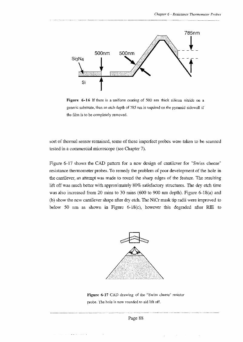
Chapter 6 - Resistance Thermometer Probes
500nm
Si
Figure 6-16 If there is a uniform coating of 500 nm thick silicon nitride on a
generic substrate, then an etch depth of 785 nm is required on the pyramid sidewall if
the film is to be completely removed.
sort of thermal sensor remained, some of these imperfect probes were taken to be scanned
tested in a commercial microscope (see Chapter 7).
Figure 6-17 shows the CAD pattern for a new design of cantilever for "Swiss cheese"
resistance thermometer probes. To remedy the problem of poor development of the hole in
the cantilever, an attempt was made to round the sharp edges of the feature. The resulting
lift off was much better with approximately 80% satisfactory structures. The dry etch time
was also increased from 20 mins to 30 mins (600 to 900 nm depth). Figure 6-18(a) and
(b) show the new cantilever shape after dry etch. The NiCr mask tip radii were improved to
below 50 nm as shown in Figure 6-18(c), however this degraded after RIB to
Figure 6-17 CAD drawing of the "Swiss cheese" resistor
probe. The hole is now rounded to aid lift off.
Page 88

Chapter 6 - Resistance Thermometer Probes
(a) (b) (c)
Figure 6-18 (a) & (b) SEM micrographs of "Swiss cheese" cantilevers after the increased dry etch. (c)
SEM micrograph of the Nichrome dry etch mask before etching which will form the sharp tip.
approximately 100 nm due to mask erosion. The metal wire was patterned as before, but
with a greater success rate due to the improved cantilever definition. The pad level caused
unexpected problems in that in a large fraction of the pyramids were capped with thick
gold. This was attributed to the effect of the extended dry etch on flat areas of the
specimen. Figure 6-18 (b) shows the etched surface where the silicon nitride has been
partly removed. The remaining silicon appears to have been roughened by the etch. This is
often called "grass", and is the result of the extended dry etch damaging the silicon
surface. The adhesion of the pad layer was later fixed by increasing the resist thickness for
the pad layer.
Figure 6-19 shows several SEM micrographs of released "Swiss cheese" resistance
thermometer probes which avoided capping of the pad layer. All the sacrificial metal
Figure 6-19 SEM micrographs of released "Swiss cheese" resistor probes with magnified images of the
tip.
Page 89

Chapter 6 - Resistance Thermometer Probes
Figure 6-20 SEM (pre-release) and optical micrographs of enhanced sensitivity side resistor probe.
surrounding the probe tips has detached during release this time. It can be seen from the
side profiles that the cantilevers were bowed slightly due to the stressed Pd wires. This
was reduced when an enhanced sensitivity version of the side resistor probe was produced
(Figure 6-20). Electrical probing confirmed that the probes were continuous and similar to
the Bowtie probes in resistance. Testing of the enhanced sensitivity probes goes on.
[1] A. Hammiche, D. J. Hourston, H. M. Pollock, M. Reading, and M. Song, "Scanning thermalmicroscopy - subsurface imaging, thermal mapping of polymer blends, and localizedcalorimetry," Journal Of Vacuum Science & Technology B, vol. 14, pp. 1486-1491, 1996.
[2] A. Hammiche, M. Song, H. M. Pollock, and D. J. Hourston, "Phase-separation of miscibleblends - study by sthm and m-t dsc," Abstracts Of Papers Of the American Chemical Society,vol. 212, pp. 186-PMSE, 1996.
[3] A. Hammiche, M. Reading, H. M. Pollock, M. Song, and D. J. Hourston, "Localized thermalanalysis using a miniaturized resistive probe," Review Of Scientific Instruments, vol. 67, pp.4268-4274, 1996.
[4] A. Hammiche, H. M. Pollock, M. Song, and D. J. Hourston, "Subsurface imaging by scanningthermal microscopy," Measurement Science & Technology, vol. 7, pp. 142-150, 1996.
[5] Solid State Physics: Cambridge University Press, 1974.
[6] The Solid State: Oxford Science Publications, 1978.
[7] J. W. Gardner, "Microsensors," Wiley Press, 1994.
[8] H. E. Sostmann, "Fundamentals of thermometry Part 3 - The standard platinum resistancethermometer," www.its_90.com.
[9] H. E. Sostmann, "Fundamentals of Thermometry Part 1," www.its_90.com.
[10] A. Hammiche, H. M. Pollock, M. Reading, M. Claybourn, P. H. Turner, and K. Jewkes,"Photothermal FT-IR spectroscopy: A step towards FT-IR microscopy at a resolution better thanthe diffraction limit," Applied Spectroscopy, vol. 53, pp. 810-815, 1999.
Page 90

Chapter 7 - Studies at CASE Collaborator
7 Studies at CASE Collaborator
7.1 Introduction
As part of the EPSRC CASE collaboration, it was necessary for the author to spend a
period of three months in the employ of the project sponsors, Motorola. It was decided
that this should take place in Mesa, Arizona at the Materials Characterisation Laboratory
(MCL) which was then part of the Materials Research and Strategic Technologies
(MRST) division. A programme of work was devised which included use of a commercial
AFM by Digital Instrumenti\DI), which had been modified for SThM. The remit of the
project was to investigate the application of SThM with specimens relevant to the industrial
activities at Motorola, and where possible to make a comparison of the commercial SThM
probes with Glasgow thermal probes.
7.2 Thermal Probes
The probes used in this investigation came from two sources, DI and Glasgow University,
and were made using Focused Ion Beam (FIB) and Electron Beam Lithography (EBL)
respectively. All probes were resistance thermometer probes.
The DI probes, fabricated by Mark Wendman ofDI, are conventional silicon nitride AFM
probes" which have been modified to incorporate a resistor in the form of a metal strap
over the tip apex. The probes consist of two pads for electrical connection made by first
coating the front face of the probe with AI, then using an FIB to mill a 1 urn gap all the
way up the substrate, onto the cantilever and over the tip. In a second step, again using the
FIB, a platinum strap is deposited across the two pads over the tip apex. The resistances
are trimmed if necessary by adding more metal in a second deposition stage to achieve a
probe resistance of 1-2 kO. Due to the significant thickness deposited (200-400 nm), the
initial tip radius of around 100 nm changes to a roughly circular flat apex which is
approximately 750 nm in diameter. Figure 7-1 shows a set of SEM micrographs of the
probes.
Two types of Glasgow University probe were used, the "Bowtie" (see Section 6.3) and
improved access ("side") resistance probes (see Section 6.5). Unfortunately, both kinds
of probe were in a relatively immature state of development, and as such most examples
were sub-optimal at this time. As described in Chapter 6, an unwanted shroud of partly
24 Digital Instruments 112 Robin Hill Rd, Santa Barbara, CA, USA.25 Nanosensors GmbH IMO-Building, Im Amtmann 6, Wetzlar-Blankenfeld, Germany.
Page 91
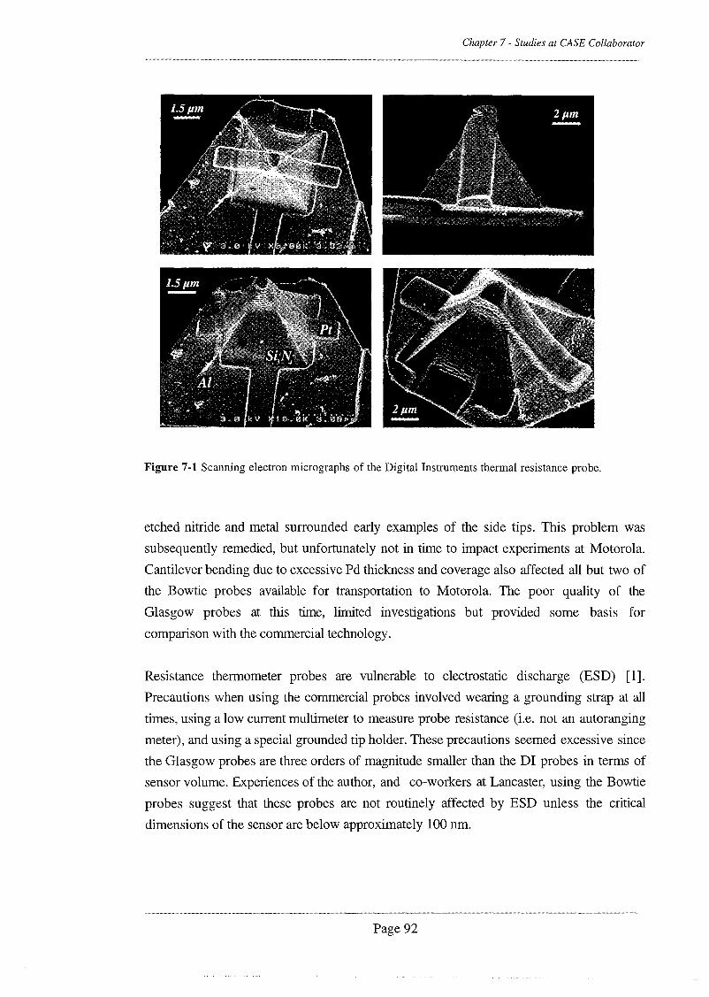
Chapter 7 - Studies at CASE Collaborator
Figure 7-1 Scanning electron micrographs of the Digital Instruments thermal resistance probe.
etched nitride and metal surrounded early examples of the side tips. This problem was
subsequently remedied, but unfortunately not in time to impact experiments at Motorola.
Cantilever bending due to excessive Pd thickness and coverage also affected all but two of
the Bowtie probes available for transportation to Motorola. The poor quality of the
Glasgow probes at this time, limited investigations but provided some basis for
comparison with the commercial technology.
Resistance thermometer probes are vulnerable to electrostatic discharge (ESD) [1].
Precautions when using the commercial probes involved wearing a grounding strap at all
times, using a low current multimeter to measure probe resistance (i.e. not an autoranging
meter), and using a special grounded tip holder. These precautions seemed excessive since
the Glasgow probes are three orders of magnitude smaller than the Dr probes in terms of
sensor volume. Experiences of the author, and co-workers at Lancaster, using the Bowtie
probes suggest that these probes are not routinely affected by ESD unless the critical
dimensions of the sensor are below approximately 100 nm.
Page 92

Chapter 7 - Studies at CASE Collaborator
7.3 Experimental Setup
Facilities at Motorola MRST in Phoenix, Arizona were substantial and included a Digital
Instruments Dimension 3000 AFM, a Micrion Focussed Ion Beam (Fill) machine, a
Physical Electronics Scanning Auger Spectrometer, Hitachi SEMs and Zeiss optical
microscope.
The Dimension 3000 AFM includes an eight inch motorised stage, piezo tube scanner [2]
with 90 urn of travel in x and y, top view CCD camera, beam deflection force detection [3]
(see Figure 1-2) and automatic tip approach. In this particular AFM, the specimen is fixed
during scanning and the tip moved in x, y, and z. The thermal option for the machine was
also fitted which changes the AFM so that it can be used with the DI thermal tips.
Modifications include the incorporation of a Wheatstone bridge and operational amplifier
in the scanning head with external gain and balancing resistor controls. The thermal probe
holder differs from the conventional DI holder (Figure 7-2) in that it does not have a
dithering Z piezo but instead has a two pronged metal clip for making electrical connection
to the probe. The prongs are electrically insulated from each other during scanning,
however a rotating bar at the base of the clip allows the prongs to be either lifted for
mounting the probe or shorted together for protection from ESD and transient effects
during connection to the microscope. Fortunately, no further modification of the tip holder
or electronics was needed to use the Glasgow probes in the DI machine. The twin Au pads
on the Glasgow probes were ideally placed for good electrical connection and the
resistance of the probe was sufficiently similar to that of the DI probes to be able to be
balanced by the variable balancing resistor already present in the modified electronics.
Due to resistance differences between the DI thermal probes, a procedure for normalising
the sensitivity of the probes was performed before scanning. The beam deflection laser,
Figure 7-2 (a) Standard tip holder with single metal clip. (b) Thermal holder
with twin clips and rotating bar.
Page 93

Chapter 7 - Studies at CASE Collaborator
which is aligned to the cantilever for force detection, is used to heat the probe. The voltage
across the probe is then adjusted to be approximately 6 V by trimming the amplifier gain
and variable resistors (2 kQ and 200 Q) on the balancing arm of the amplifier. Current in
the DI probes is typically 400~ during normal operation, depending on the resistance of
the probe. The DI microscope does not allow for the current in the probe to vary (other
than due to external effects) so modulating the probe current and dectecting with a lock in
amplifier was not possible, i.e. only de heating and detection was available.
7.4 Probe Characteristics
Both the DI and Glasgow probes are bimaterial strips since they have metal coatings on
the front face of a silicon nitride cantilever. Bimaterial strips bend when heated, and this
was also found to be the case with the SThM cantilevers. Sources of cantilever heating
include
• Electrical heating from biasing of the integrated resistor.
• Optical heating from the force sensing laser.
• Conduction of heat to and from a specimen through tip contact.
• Convection from to and from a specimen across an air gap.
• Radiative exchanges of heat from specimen to cantilever.
As the cantilever is heated or cooled and bending occurs, care must be taken to anticipate
and compensate for the resulting changes in force of contact with the specimen. Issues like
tip wear and specimen deformation can be greater if excessive force is used, and the tip
may intermittently lose contact with the specimen if too small a contact force is used. In
order to measure the heating of the cantilever, temperature-distance curves for each of the
probes was aquired. These graphs are plots of temperature (measured using the integrated
resistor) versus distance from a specimen. It is useful to compare the temperature-distance
curves with simultaneously measured force-distance curves, which are plots of cantilever
deflection (measured using the force sensing laser) versus distance from specimen. The
coincidence of physical events such as contact with the specimen and thermal events such
as a step change in probe temperature may be observed using this technique.
The force-distance and temperature-distance curves for the three different probes are
shown in Figure 7-3. The side and bowtie probes were contacted to gold surfaces for these
curves, whereas the DI probe was contacted to a silicon surface. The curves show that in
the case of the DI tip, the temperature of the probe drops as it nears the surface
presumably due to radiative and convective heat transfer into the approaching surface. The
cantilever responds by deflecting towards the specimen surface. At the point of contact
Page 94

Chapter 7 - Studies at CASE Collaborator
with the surface the temperature of the probe drops abruptly, due to heat conduction at the
tip, and the cantilever attempts to bend further towards the specimen. This is prevented
however by the presence of the surface and so results in the application of a significant
force to the surface. The cantilever deflects away from the specimen as the force is
increased and the probe resumes its gradual decrease in temperature because of decreasing
air gap between the cantilever and the surface. Figure 7-4 shows a graphical representation
of the cantilever descent and the associated heat transfer and cantilever deflection.
The hysterisis in the temperature-distance curves is caused when the probe is retracted and
allowed to bend towards the specimen surface (while maintaining contact). This appears
similar to the pullout force experienced by conventional tips due to the ubiquitous water
layer found on surfaces in air at room temperature. An increase in these capillary forces is
inevitable because of the greater tip radius of the DI thermal probe, but it is the view of the
Force-Distance2 l='ositi.on - 1.00 U/div
Setpo'int
Force-Distance
Tip1)f.'11cclilJIl........................................:d~'------- -I 0,05 UId!v
Z position - 5.00 O/div
(a) DI Probe
Left Trace- '----c---:-c----=--=--:-:-:.,-------'
Til'Dejltct{MI
0.25 (l/d!v
Setpoint
Resi.sttorVoltage
0.10 Wd!v
Setpoil'lt
ResistorHlltage
0.01 U/div
Setpo.int
Temp-distance'Z posi t tow - 1.00 U/dill
Temp-distanceZ position - 5.00 U/div
Ri yht: Tr<Kce'--__::---:-.,----=--::-"""'"':--__--'
'til'J)efif!~tioll
0,25 UId;v
(c) Bowtie Probe
Resistor·Voltage
0.05 Wd!v
Force-Distance
Z PClsition - 2.50 U/div I )IRetracting-~- Extend i ng
Se tpc i rrt
Temp-distance
Z rost tion - 2.50 U/-diu
Figure 7-3 Force/Distance (top) and Temperature/Distance (bottom) curves for (a) the DI
thermal probe, (b) the Glasgow improved access resistance thermometer probe, and (c) the
Glasgow Bowtie probe.
Page 95

Chapter 7 - Studies at CASE Collaborator
(a) (b) (c) (d)
Figure 7·4 (a) Unheated probe. (b) When heated with the laser, the probe bends away from the
surface. (c) As the probe descends it loses some of its heat to the surface begins to bend back towards
the surface. (d) When the probe makes contact, the probe experiences a step decrease in temperature and
would like to assume its unheated position (dashed lines). This is not possible due to the presence of
the surface and so a force is exerted on the surface.
author that the hysteresis is dominated by thermally induced bending of the cantilever. As
the tip is retracted and loses contact with the specimen, it suddenly loses all conductive
heat-sinking. The tip rapidly heats up to its pre-contact temperature after losing contact,
and deflects abruptly away from the surface to its original position. Performing this
experiment in vacuum, where most of the surface water layer is removed, would give a
better understanding of the contribution of the capillary effect to this observation. It is
important to note that if minimum force scanning is desired, then the position just before
the tip loses contact on retraction is the point of zero force between tip and specimen, not
at the point of contact during approach.
The improved access and Bowtie probes showed similar effects to those seen with the DI
tip but with two important differences. Firstly the polarity of the resistance change was
opposite to that with the DI tip, and secondly the magnitude of the temperature induced
deflections was significantly less than that for the DI tip. The polarity difference was
attributed to the different material composition of the resistors. In the case of the Glasgow
probes, the resistors were deposited using electron beam evaporation of a pure electronic
grade palladium source. The DI resistor was deposited by using an FIB to decompose an
organometallic and, although nominally platinum, such deposits are known to contain large
amounts of carbon and oxygen (plus other stray contaminants from the chamber) [4].
With enough carbon contaminant, a material may change its properties from those of a
metal (where resistance increases with heat due to increased scattering) to those of a
Page 96

Chapter 7 - Studies at CASE Collaborator
semiconductor (where resistance can decrease due to increased carrier concentration).
Auger electron spectroscopy (ABS) [5] was carried out on the resistive element on the DI
thermal tip (Figure 7-5) by Bridget Rogers of Motorola [6]. A 10 kV, 20 nA primary
beam was used for the analysis after 1 kV Argon ions had been used to remove surface
carbon. Measurements revealed the resistor composition to be 60% C, 35% Pt and 5% o.The excessive carbon content of the resistive element explains why the DI probe acts as a
negative temperature coefficient resistor, and is probably also responsible for the high
sensitivity of the probe. A draw back however to this method of resistor fabrication, where
contamination determines the probe characteristics, is that contamination by its nature is
unpredictable. Although not explored further, it is likely that reproducibility of calibration
would be poor with DI probes.
The other difference between the DI and Glasgow probes was the magnitude of the
temperature induced deflections of the probes. Comparison of the probes in the force
distance curves showed that the Glasgow probes were less prone to the large cantilever
deflections observed with the DI probes. The DI probe suffered approximately 700 nm of
bending when contact was lost on retraction, compared to approximately 35 nm for the
side probe and 200 nm for the Bowtie probe. The reason for this would appear to be the
difference in shape, composition and thickness of the metal coatings on the front faces of
o
PI
c
N a
500 1000
Electron Energy (eV)
1500
PI
2000
Figure 7-5 Scanning Auger spectrum of the material that formed the resistive element on the DI
thermal tip. The composition was calculated to be 60% C, 35% Pt and 5% 0 (analysis performed by
Bridget Rogers of Motorola).
Page 97

Chapter 7 - Studies at CASE Collaborator
the Glasgow probes, which reduces the heat absorbed by the laser and the bimaterial effect
with the Si3N4 cantilever. Another factor that would reduced these effects is the tip radius
of the different probes (which determines contact area). For example, the side probe has a
nominal tip radius of 100 nm compared to approximately 500 nm for the DI tip. The
Bowtie has a sensor dimension of approximately 150 nm but a tip radius of approximately
1.5 urn, Capillary forces may be significant with the Bowtie probe since it has a large flat
contact area. The coverage and nature of the metal on the cantilever, which affects the heat
absorbed by the probe from the laser, would appear to be a stronger influence however
since the thermal deflections of the Bowtie are more than three times less than that of the
DI probe. Yet another factor to be considered is the relative tip height of the probes. This
determines the distance of the cantilever to the specimen at the point of contact, and is
approximately 20 urn for the Glasgow probes compared to just under -l um for the DI tip.
It has been shown that heat may be transferred to and from a cantilever through an air gap
[7, 8]. Maximising this air gap reduces this effect and so a taller pyramid is preferable if
cantilever-specimen interactions are to be minimised.
An advantage of the DI probe was that in comparison to the side and Bowtie probes, the
signal levels were typically an order of magnitude greater. This was attributed to the larger
series resistance and smaller contact area inherent in the Glasgow probe design (later
improved using the enhanced sensitivity design - see Section 6.4). This was compensated
for by increasing the gain of the thermal signal amplifier in the DI microscope electronics.
The greater sensitivity of the DI probe is attributed to the material difference between the
probes.
DIProbe Glasgow Side Resistor
Fabrication Method FIB EBL
Batch Size 1 60 or 240
Tip Radius 500nm 100nm
Tip Height 4!lm 20 urn
Sensor Material PUC Pd
Resistor Thickness 200-300 nm 50nm
Resistor Size l um x Sjrm 100 nm x 200 nm
Resistance 1-2kQ 1-2kQ
Figure 7-6 Table comparing the Dr and Glasgow probes
Page 98

Chapter 7 - Studies at CASE Collaborator
Figure 7-7 SEM cross section of passivated AICu wires.
A summary of the differences between the side and DI probe is shown in Figure 7-6. The
DI probe was used for most of the following experiments, however the side probe was
also used at times to verify results and look for probe-specific artefacts.
7.5 Passivated Wires
Initial investigations with the DI thermal probe involved scanning some AlCu wires under
250 nm of passivation. Figure 7-7 shows a SEM cross section of the structure. The
unheated wires were scanned normal to the direction of the wires. For analysis with the
thermal tips, scan rates were low (0.2 Hz or below) in order to avoid tip damage and allow
the feedback loop time to track the surface. Figure 7-8 shows four images scanned in
different modes. Topographic analysis was performed using tapping and contact mode
scanning with conventional probes (silicon and silicon nitride respectively). Thermal
scanning, which yields a topographic image and a simultaneous thermal image, was
performed using the DI thermal probe. Contact and tapping mode were used to verify the
topography of the specimen, since it was shown earlier that temperature changes cause
deflections in the thermal probe.
In both the tapping and contact mode images (Figure 7-8(a) and (b», the surface
roughness of the passivation covering the wires appears to be randomly oriented, however
in the topography image with the thermal probe a large granularity is seen. This
granularity is approximately 500 nm in size, which roughly matches the tip dimensions
and so could be a repeated image of the tip shape. In the contact mode image and
topography images using the thermal probe, the wires appear broadened compared to the
tapping mode image. This is due to a larger tip opening angle which was measured by
Page 99

Chapter 7 - Studies at CASE Collaborator
Figure 7-8 Passivated AlCu Wires (see Figure 7-7). (a) Tapping mode image using conventional silicon
probe. (b) Contact mode image using conventional silicon nitride probe. (c) Heat flow image using DI
thermal probe. (d) Topography image using DI thermal probe acquired simultaneously with (c).
looking at cross sections of the scans to be approximately 70 degrees for contact and 35
degrees for the tapping mode, which agrees with the manufacturer's specification for each
probe.
The thermal image in Figure 7-8(c) is strikingly different from all the other images.
Firstly, the edges of the wires appear brighter than the centre. This is explained by the tip
specimen contact area decreasing as the probe travels over an edge, producing an increase
in probe temperature (see Figure 7-9). Secondly, there is a very high resolution granular
structure in the body of the wires which is mirrored in part by the topography image using
the thermal probe (Figure 7-8(d)). The origin of this contrast is thought to be due to
surface roughness and differences in tip contact causing changes in heat transfer from tip
to specimen. No such shapes are observed with the conventional tips however. Another
hypothesis to explain this decoration of the passivated wires is that somehow the grain
structure of the underlying metal is affecting the thermal tip. Perhaps differences in the
thermal conductivity of different crystal orientations or even the roughness of the metal is
being detected by the thermal probe.
Page 100

Chapter 7 - Studies at CASE Collaborator
Sample
Hot
~, Cold
Figure 7-9 Tip losing heat over an edge. Note the representation of
the water layer which is present on all surfaces at ambient.
To see if there was a correspondence between the grain size of the underlying Aleu and
the features in the thermal image, a different part of the specimen containing a depassivated
area of the same metal layer was scanned using tapping mode AFM (Figure 7-10 (a». The
granular thermal features in Figure 7-8(c) are approximately 0.5 urn in diameter. The
roughness of this depassivated surface consists of larger features, also about 0.5 urn in
size, which contain finer structure on the 100 nm scale. Whether this image clearly
represents the Al grain size is unclear since post deposition processing can artificially
roughen the surface. In order to observe the metal grains based on their crystal orientation
therefore, a portion of the passivation on the original wires was removed using FIB
milling. The FIB delineates the grains by etching different crystal orientations at different
rates (due to channelling). Figure 7-1O(b) shows an ion induced electron image from the
FIB in which shows the grains after FIB milling. It is obvious from this image that the
grain size is appreciably larger than the shapes seen in the thermal image. This image does
not show all the grains since the angle of incidence of the milling beam was fixed, however
(a) (b)Figure 7-10 (a) Tapping mode image of unpassivated AICu metal film. (b) FIB Image of
depassivated AICu wires.
Page 101
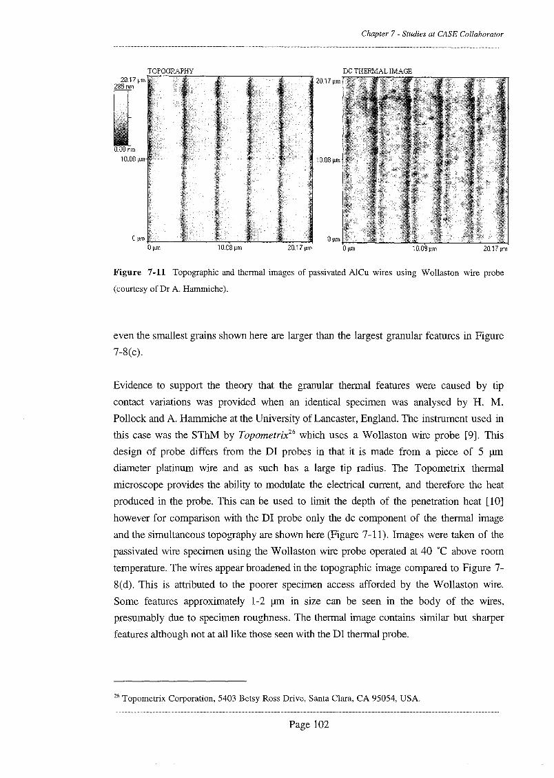
Chapter 7 - Studies at CASE Collaborator
20.17J,lm10.03um
DCTHEP.MALlMAGE20.17~lm
10.03 um
Op.m20.17J,lm OJ,lm10.0BJ,lm
OlAffi-l"-__
ourn
TOPOGRAPHY20.17jJ.ffi
2S5nm
O.OOnm10.0B pm
Figure 7-11 Topographic and thermal images of passivated AICu wires using Wollaston wire probe
(courtesy of Dr A. Hammiche).
even the smallest grains shown here are larger than the largest granular features in Figure
7-8(c).
Evidence to support the theory that the granular thermal features were caused by tip
contact variations was provided when an identical specimen was analysed by H. M.
Pollock and A. Hammiche at the University of Lancaster, England. The instrument used in
this case was the SThM by Topometrix" which uses a Wollaston wire probe [9]. This
design of probe differs from the DI probes in that it is made from a piece of 5 urn
diameter platinum wire and as such has a large tip radius. The Topometrix thermal
microscope provides the ability to modulate the electrical current, and therefore the heat
produced in the probe. This can be used to limit the depth of the penetration heat [l0]
however for comparison with the DI probe only the de component of the thermal image
and the simultaneous topography are shown here (Figure 7-11). Images were taken of the
passivated wire specimen using the Wollaston wire probe operated at 40°C above room
temperature. The wires appear broadened in the topographic image compared to Figure 7
8(d). This is attributed to the poorer specimen access afforded by the Wollaston wire.
Some features approximately 1-2 urn in size can be seen in the body of the wires,
presumably due to specimen roughness. The thermal image contains similar but sharper
features although not at all like those seen with the DI thermal probe.
26 Topometrix Corporation, 5403 Betsy Ross Drive, Santa Clara, CA 95054, USA.
Page 102
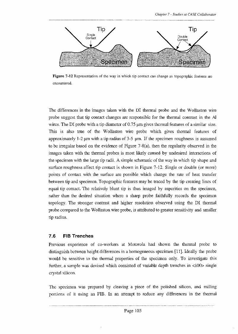
Chapter 7 - Studies at CASE Collaborator
Tip
Figure 7-12 Representation of the way in which tip contact can change as topographic features are
encountered.
The differences in the images taken with the DI thermal probe and the Wollaston wire
probe suggest that tip contact changes are responsible for the thermal contrast in the AI
wires. The DI probe with a tip diameter of 0.75 urn gives thermal features of a similar size.
This is also true of the Wollaston wire probe which gives thermal features of
approximately 1-2 urn with a tip radius of 3-5 urn. If the specimen roughness is assumed
to be irregular based on the evidence of Figure 7-8(a), then the regularity observed in the
images taken with the thermal probes is most likely caused by undesired interactions of
the specimen with the large tip radii. A simple schematic of the way in which tip shape and
surface roughness affect tip contact is shown in Figure 7-12. Single or double (or more)
points of contact with the surface are possible which change the rate of heat transfer
between tip and specimen. Topographic features may be traced by the tip creating lines of
equal tip contact. The relatively blunt tip is thus imaged by asperities on the specimen,
rather than the desired situation where a sharp probe faithfully records the specimen
topology. The stronger contrast and higher resolution observed using the DI thermal
probe compared to the Wollaston wire probe, is attributed to greater sensitivity and smaller
tip radius.
7.6 FIB Trenches
Previous experience of co-workers at Motorola had shown the thermal probe to
distinguish between height differences in a homogeneous specimen [11]. Ideally the probe
would be sensitive to the thermal properties of the specimen only. To investigate this
further, a sample was devised which consisted of variable depth trenches in <100> single
crystal silicon.
The specimen was prepared by cleaving a piece of the polished silicon, and milling
portions of it using an FIB. In an attempt to reduce any differences in the thermal
Page 103

Chapter 7 - Studies at CASE Collaborator
properties of the material due to ion implantation, an area (1OOx100 urn) of the specimen
surface was milled to implant gallium ions at a dose of approximately 5 nC/flm2 over the
whole of the working area. Three 5x5 urn trenches were then milled at depths of 80 run,
160 nm and 320 nm. Figure 7-13(a) is a topographic scan of the specimen using a
conventional silicon tapping mode probe, and clearly shows the differences in trench
depth. Figure 7-13(b) shows a thermal scan of the same area using a DI thermal probe. It
can be seen that the probe temperature decreases with increasing trench depth. Similar
enhancement of surface roughness to that in Figure 7-8(c) can be seen in this thermal
image at the bottom of the trenches. This roughness is caused by the FIB milling which
may mask surface contaminants or magnify imperfections in the original surface. Using
conventional tapping mode AFM, the roughness at the bottom of the deepest trench was
measured to be 7 nm (rms), compared to 0.15 nm (rms) for the unetched surface. In
addition to the familiar enhancement of topographic features however it is clear that there a
trench depth dependence to the temperature signal. This was attributed to the proximity of
the cantilever to the top surface since this would appear to be the only parameter that is
changed between trenches. The temperature-distance curves for the DI probe confirm that
the temperature of the probe drops as the cantilever approaches the specimen out of
contact. A separate measurement [12] showed this transfer of heat from tip to specimen to
occur over a range of 20 urn from the surface.
Figure 7-13(c) is a thermal image of the same specimen using a Glasgow side probe. It
appears that this probe does not distinguish between the different trench depths to the
same extent as the DI probe. The side probe does show a decrease in temperature with
increasing trench depth like the DI probe, but the magnitude of this decrease is small in
comparison. An indication of why this is the case may be seen in the force-distance curves
in Figure 7-3. Some bending occurs in each of the cantilevers before contact with the
specimen is made and corresponds to a drop in probe temperature. The heat loss and heat
'0.0 ITO""30.°1°.5
""
.20.0 0.0 J,Ioo
10.0
°10.0 20.0 30.0 40.0
~'IJ30.°1°.
3
20.0 0.0
10.0
.°20.0 30.0 '10.0.. ro',o 20.0 :W.O
::r:0.0.ao.c
10.0
.·040,0
Figure 7-13 FIB Trenches in Silicon (a) Topographic image scanned in tapping mode using a
conventional silicon probe. (b) Heat flow image using a DI thermal probe. (c) Heat flow image using a
Glasgow side resistor probe.
Page 104

Chapter 7 - Studies at CASE Collaborator
induced bending is due to the presence of the specimen surface (gold for the Glasgow
probes and silicon for the DI probe) and is presumably due to radiative or convective heat
transfer from probe to specimen. Calculated values for the three graphs show that each
probe deflects approximately 0.1 nm for a 1 nm decrease in tip-specimen spacing. It is
clear however that the DI probe loses more heat, and deflects more than the Glasgow
probes when near a surface since the silicon specimen used with the DI probe conducts
heat less well than the gold used with the Glasgow probes. Other issues that affect this
transfer of heat when the probe is out of contact are
• Magnitude of electrical heat produced at the tip.
• Absorption of the force sensing laser by the cantilever (optical heating).
• Distance of the cantilever from the specimen.
• Height and shape of the tip.
• The geometry of the resistive heater.
• Coverage and shape of metal layers on the cantilever.
Insufficient data was collected to determine which (if any) of these variables dominates,
however one important characteristic is the tip height. The tip height effectively determines
the distance of the cantilever from the specimen when in contact. The Glasgow probes
have a tip height of 18-20 urn whereas the DI probe has a tip height of 4 urn. Therefore if
the probe tip is a given distance from the specimen, the cantilever of the DI probe is always
14-16 urn closer to the specimen than that of the Glasgow probe.
7.7 Angle Cut Specimen
In order to chemically and electrically protect integrated circuits they are often coated with
a thick dielectric layer. To investigate the sub-surface imaging capabilities of the
microfabricated thermal probes through such passivating material (silicon oxide in this
case), structures such as those shown in Figure 7-14 were imaged. The structures were
designed to test electromigration effects in aluminium based wires, but also served as
samples with thermal features passivated in such a way as to present a flat surface to the
thermal probes. The wires were sandwiched between layers of silicon oxide, and the
passivation was approximately 1.8 urn thick above the wires. In Figure 7-l4(a) voids
between the wires are seen. This is due to overhang of material during deposition which
closes up the gap between the wires without filling it.
Although the structures were capable of electrical connection (the centre wire of the
structure shown in Figure 7-14(a) was terminated in 100xlOO urn pads), these
experiments were conducted with the specimen unconnected.
Page 105

Before
Chapter 7 - Studies at CASE Collaborator
After
(a) (b)Figure 7-14 Electromigration Structures. (a) Schematic and SEM of three AlCuW wires buried
under silicon oxide. (b) Schematic and SEM of the same specimen after an angular FIB cut made at
15" wrt to the surface plane.
Scans using the DI thermal tip on an unmodified specimen showed no evidence of the
sub-surface features. The same high resolution tip effects observed in previous
experiments were apparent, but no contrast relating to the three buried wires was seen. To
thin the passivation, the specimen was placed in the FIB and trenches similar to those
made in the silicon wafer were milled. The milling was timed to give a variety of depths,
and although the mill rate was poorly controlled due to the heterogeneous nature of the
passivation, a range of depths from 0.3 urn to 211m was achieved. Doses varied from 5 to
10 nC/l1m2• For passivation thicknesses above 0.1 11m no evidence of the sub-surface
voids was seen. The images shown in Figure 7-l5(a) and (b) were acquired at 100 nm.
The topographic image shows the large ridge covering the wires and a large dimple, which
is due to contamination or a defect accelerating the mill, but no other features. The thermal
image on the other hand clearly shows the voids between the wires which appear as bright
tramlines in the centre of the image (arrowed). The contrast is correct in that the tip
Page 106

Chapter 7 - Studies at CASE Collaborator
appears to be losing less heat over the voids, which are assumed to be air filled. This may
be considered to be a sub-surface thermal image since features can be seen that
correspond to known structures buried in the specimen. Furthermore there is no
topographic evidence of these features.
It was difficult to time the milling to give a range of depths near to the 0.1 urn thickness
which would help pinpoint a maximum passivation thickness for detection of the sub
surface features therefore an alternative approach was used. An angular cut was made with
the FIB down into the wires and through to the substrate below. Figure 7-14(b) shows an
SEM micrograph and schematic drawing of the angle cut structure. By cutting at an angle,
the scan surface was defined by the FIB side wall. The cut started at the top of the
passivation and was angled down into the specimen. Had the cut been made the other way
(starting at the wires and milling up at an angle) the voids and the metal wires would have
caused non-uniform milling and a rough side wall. The side walls of an FIB cut are much
less rough than at the bottom of a trench in general because the beam is tangential to the
surface and gives a polishing effect. With trench cutting any surface debris or pits on the
5.0
o 2.5 5.0
5.00
7.5
2.00
(a),·0
8.00
u"
10.0 D,oo.0 ""
7.5 I"50.0 n.
0.0 nH5.0
2.5
(c)U"
o
2.00 4.CO 5.00
5.00
1:(~0.3 V ~
.' ~5.00 . 0.1 V ~
.;;;
'"4.00 0.0 V ::.:;
(b)U"
10.0 i'.D V'"I ~
: '"I _I _
~7.S O.S U ....
~
'"';;;'"0.0 v ::.:;
2.5
(d)
Figure 7-15 Sub-surface images using the Dr probe. (a) Topography image of buried wire (O.7J.lm
passivation thickness). (b) Corresponding heat flow image. Voids between wires are arrowed. (c)
Topographic image of angle cut passivated wires. (d) Corresponding heat flow image.
Page 107

Chapter 7 - Studies at CASE Collaborator
original surface are amplified down onto the final surface. An FIB sidewall may be
incrementally polished by repeated milling with finer spots, but this was not possible here
due to time constraints.
The finished specimen presented a continuum of passivation thickness from 1.8 urn down
to the bare metal wires, followed by a section down through the wires and beyond. Scans
of this surface using a DI thermal tip are shown in Figure 7-15(c) and (d). The passivation
thickness is greatest at the bottom of the images. The topographic image shows two large
trenches which were caused when the voids were breached and are arrowed in Figure 7
14(b). The thermal image clearly shows the thermal conductivity difference between the
aluminium wires (the three dark stripes) and the passivation. The corrugation which can be
seen in both topographic and thermal images is caused by the FIB raster scan (spot size
was 0.1 urn) and was measured to be 1 nm p-p using tapping mode AFM with
conventional silicon probes.
Areas of interest in the thermal image were the two white tails protruding from the three
stripes (which represent the metal wires). These are caused by the voids between the wires
which alter the effective thermal conductivity of the specimen. If the voltage across the
probe in air (far away from the specimen) is offset to be zero, the relative voltages when
contacted to the passivated voids, Si02 and metal wires were measured to be 25 mY, 100
mVand 135 mV respectively. Roughly twice the contrast is thus produced by the sub
surface feature compared with the AI relative to the Si02• This explains why the voids can
seen in Figure 7-15(b) at a depth of 100 nm without evidence of the metal lines. From the
known angle of the cut (15°) and the measured lateral extent of the thermal features
corresponding to the voids (light streaks), the maximum depth for resolution of the voids
was calculated to be 225 nm (± 25 nm), at which point the contrast due to the sub-surface
2.00 4.[)O B.DO
8.00 0.2 V '"0.0
'".::::~
6.00 0.1 U 10".
.::'".;;;'"0.0 u ::c:
4.00
(a)
O,L V ~
0.0.§,,0-0,1 IJ ....
s.::='"'""0,0 1.I Q::::.
(b)
Figure 7-16 Side resistor images of angle cut passivated wires. (a) Heat flow image with shroud
collapse mid scan. (b) Complete heat flow image post collapse (contrast reversed).
Page 108

Chapter 7 - Studies at CASE Collaborator
voids was equal to that due to the residual topographic corrugation.
A side resistor probe was used to scan the same specimen. Unfortunately the only side
probes available during this experiment were those which had been poorly etched and
featured a silicon nitride and metal shroud round the tip apex (see Section 6.5). Initial
thermal images were of variable quality which was attributed to the shroud causing poor
thermal contact with the specimen. Figure 7-16(a) shows what is thought to be the fragile
shroud collapsing part way through a scan due to tip wear, thus allowing the real tip and
sensor to image the specimen. The image switches suddenly to give a clearer image of the
wires and voids that corresponds well to the image taken with the DI tip. Figure 7-l6(b)
shows a complete scan after the shroud has disappeared. The contrast in this image has
been artificially reversed for comparison with the image using the DI tip (Figure 7-15(d)).
Note that despite the normalisation of the different probe sensitivities using heat from the
force sensing laser, the full scale voltage in the DI probe image is five times greater than
that of the side probe. This is attributed to the material difference between resistors and the
inherently poorer thermal contact afforded by the sharper side probe. Despite this, the
signal to noise was measured from the images to be 18.5 dB for the DI probe and 27 dB
for the side probe. The lower noise in the side probe is attributed to the purity of the Pd
resistor relative to the carbon contaminated DI resistor.
[1] A. P. Whitehead, P. K. Footner, and B. P. Richards, "ESD-Induced Electromigration; A newVLSI failure mechanism.," Proc. ISTFA, pp. 214-220, 1984.
[2] G. Binnig and D. P. E. Smith, "Single-tube 3-dimensional scanner for scanning tunnelingmicroscopy," Review Of Scientific Instruments, vol. 57, pp. 1688-1689, 1986.
[3] Scanning probe microscopy and spectroscopy: Cambridge University Press, 1994.
[4] L. Johnson, Motorola MRST, Private communication 1998, [email protected].
[5] S. M. Sze, VLSI Technology: McGraw Hill, 1988.
[6] G. Mills, J. M. R. Weaver, G. Harris, W. Chen, J. Carrejo, B. Johnson, and B. Rogers,"Detection of sub-surface voids using scanning thermal microscopy," Ultramicroscopy, vol. 80,pp. 7-11, 1999.
[7] O. Nakabeppu, M. Chandrachood, Y. Wu, J. Lai, and A. Majumdar, "Scanning thermal imagingmicroscopy using composite cantilever probes," Applied Physics Letters, vol. 66, pp. 694-696,1995.
[8] H. Pollock, University of Lancaster, Private communication 1998, [email protected].
[9] A. Hammiche, M. Reading, H. M. Pollock, M. Song, and D. J. Hourston, "Localized thermalanalysis using a miniaturized resistive probe," Review Of Scientific Instruments, vol. 67, pp.4268-4274, 1996.
Page 109

Chapter 7 - Studies at CASE Collaborator
[10] A. Hammiche, D. J. Hourston, H. M. Pollock, M. Reading, and M. Song, "Scanning thenna1microscopy - subsurface imaging, thenna1 mapping of polymer blends, and localizedcalorimetry," Journal Of Vacuum Science & Technology B, vol. 14, pp. 1486-1491, 1996.
[11] W. Chen, Motorola SPS, Private communication 1997, [email protected].
[12] K. Kjoller, Digital Instruments Corp, Private Communication 1997, [email protected].
Page 110

Chapter 8 - Conclusions
8 Conclusions
8.1 Probe Fabrication
It has been shown that a variety of novel probes for scanning thermal microscopy may be
batch fabricated using nanolithography and micromachining [1-3]. Figure 8-1 shows a
table of the probes that have fabricated by the author. The probes may be split into two
distinct types: Au/Pd thermocouples and Pd resistance thermometerlheaters. Both have
been demonstrated with truncated pyramid and sharp triangular tips. Figure 8-2 shows a
schematic of the different tip shapes which have complimentary advantages. The truncated
pyramid offers good thermal contact of the sensor to relatively flat specimens. For
specimens with significant relief however, the large tip size means that the sensor may
Probe
CrossThermocouple
SideThermocouple
TripleThermocouple
Swiss·· CheeseThermocouple
BowtteResistor
SideResistor
Figure 8-1 Table of thermal probes fabricated using the generic Glasgow substrate.
Page 111

Chapter 8 - Conclusions
(a) (b)
Figure 8-2 Different specimen access and sensor contact area with (a) the truncated
pyramid and (b) sharp triangular tip.
intermittently lose contact resulting in errors in the thermal data. In contrast, the sharp
triangular tip gives better specimen access, but only a small portion of the sensor at the tip
apex is in contact with the specimen. Although not yet properly characterised, this is
expected to degrade the thermal signal to noise ratio and thermalisation time constant.
The thermocouple and resistance thermometer/heater probes differ significantly.
Thermocouples are capable of quantitative thermometry, and this is a desirable function for
a microscope probe to have. It has been shown that the Seebeck coefficient for the thin
film AulPd thermocouples used here are the same as bulk AulPd thermocouples to within
a factor two and matched to 3% on a probe. The thermocouple probes have also been
shown to produce temperature maps of a photothermal test specimen when scanned in a
conventional AFM.
The resistance thermometer/heater probes may be used in many different modes, some of
which have been presented here. Thermal conductivity imaging and thermomechanical
thermal analysis of polymers has been demonstrated in collaboration with Lancaster
University. Subsurface imaging has been also been performed using the side resistor
probe in a commercial microscope and a specimen with buried thermal features.
Some novel designs and processes for making AFM cantilevers and sensors have been
developed including selective removal of parts of the cantilever to provide self alignment of
the thermal sensor to the tip. Multiple sensors have also been fabricated on a single tip,
which demonstrates that complex patterns may be patterned on three dimensional
substrates. The multiple sensor tips may have utility in their own right for measuring tip
contact effects or high speed scanning. The limits of electron beam lithography and metal
lift off on the generic pyramidal AFM tips has also been explored. Wires 35 nm wide have
been patterned at the apices of the 20 urn high tips. The limiting factor would appear to be
the resist coating on the tip which must be thick enough to cover sharp edges yet thin
Page 112

Chapter 8 - Conclusions
enough to allow small features to be patterned. The extent and shape of the metal features
at the tip that form the thermal sensors have been varied, and were found to affect the
bending of the AFM cantilevers and sensitivity of the thermometers. In addition to this,
advances in transferring metal patterns onto three dimensional substrates have been made.
The employment of "lift-off aids", where redundant space is patterned in such a way as to
free excess metal from critical features, has been shown to be invaluable in producing
sensors with high yield.
8.2 Measurements
It is fair to say that the work presented here has not only advanced the field of scanning
thermal microscopy in terms of probe development, but also in the measurement of
thermal phenomena. Some of the highest resolution thermal images ever obtained have
been produced using the improved access thermocouple probes. The contrast was due to
changes in heat transfer between tip and a photothermal test specimen, and a resolution of
40 nm was observed. In addition to this, the temperature dependence of 70 nm
thermocouples on the triple thermocouple probes has been measured, although not
calibrated.
Much pioneering work has also been done in collaboration with Lancaster University.
High resolution thermal conductivity and thermal expansion images of polymer specimens
have been demonstrated using the Bowtie probes. Thermomechanical point measurements
have been made and phase changes in selected polymers observed. Resolutions of 100
200 nm have been achieved, and glass transitions and melting events have been identified.
Calorimetric measurements, where the heating of the probe is modulated, have just recently
been acquired [4]. Work continues at Lancaster to discover more about the contrast
mechanisms involved, and to apply the probe techniques to new fields of measurement.
Inconjunction with testing of the new micromachined probes at Glasgow and Lancaster, a
body of work has been accumulated using both Glasgow and commercial probes in a
commercial microscope. This work was carried out at Motorola - the CASE collaborator
for this project. The dependence of cantileverbending on specimen temperature while in
close proximity to the specimen, and at the point of contact, were studied. Tip contact area
variations and parasitic heat transfer to the specimen through the cantilever were identified
as significant contributors of artificial contrast. Due to the Glasgow probes having smaller
tip radii, taller tips, and less metal on the cantilever, the magnitudes of these deleterious
effects were shown to be significantly smaller than with the commercial probes. Sub
surface detection of voids in multiple layer electromigration test structures was also
achieved using thermal conductivity imaging. Angled sectioning of the structures was then
Page 113

Chapter 8 - Conclusions
used to determine that the maximum depth of penetration was over 200 nm under normal
operating conditions.
8.3 Artefacts
There would appear to be three main causes of artefactual contrast in scanning thermal
rmcroscopy.
• Tip-specimen contact area effects.
• Short range temperature induced bending of the cantilever due to contact with
specimen.
• Long range bending of the cantilever and distortion of thermal information due to
radiative and convective heat transfer from the cantilever its environment.
The most common and misleading artefact is caused by variations III tip to specimen
contact area. Strong thermal contrast corresponding solely to topographic changes in the
specimen has been observed in almost all of the thermal images produced during this
project, often obscuring temperature or thermal conductivity contrast. The effect is
dependent on sensor size, tip radius, and specimen roughness, and was seen using DI,
Glasgow and Wollaston wire probes to varying degrees. Ideally, specimens analysed by
SThM would be perfectly flat in order to eliminate the tip effects, however in practice no
specimens have yet met this criterion. Specimen preparation (FIB milling, chemical
etching, mechanical cleaving and polishing) can help to planarise surfaces of interest,
however this can be time consuming and in most cases the original thermal properties of
the specimen are expected to be drastically altered.
What is important is that the tip radius and sensor dimensions be shrunk to approximately
an order of magnitude less than the specimen micro-roughness. Undulations on the
(a) (b)Figure 8-3 (a) The specimen may be faithfully traced by the tip if the roughness is
(a) larger than the tip radius and tip opening angle or (b) much less than the tip
radius.
Page 114

Chapter 8 - Conclusions
surface should then be well resolved by the AFM, and contact with the specimen
maintained at the end of the tip. Alternatively, destructive artefacts from roughness may be
avoided if the tip is approximately an order of magnitude larger than the specimen micro
roughness. The specimen roughness may then cause high frequency spatial noise in the
thermal image, but thermal features of similar size to the tip will be resolved. In both cases,
shown diagramatically in Figure 8-3, the tip must have an appropriate opening angle to
preserve tip contact during larger scale topographic variations. This allows the specimen to
be faithfully traced by the tip and artefacts caused by bridging of valleys to be significantly
reduced.
The specimens used during this investigation can be split into two broad categories:
semiconductor structures and polymers. Inorder to determine whether SThM will become
an important analysis tool in these areas, it is useful to look at typical specimens and the
type of measurements that are most desirable. In the case of the semiconductor industry, a
key application area is measurement of the power dissipation of the millions of transistors
found on modern microprocessors. Finished die usually have large topographic variations
due the thick contact layers and many microns of passivation deposited over the whole die.
It is important that these structures are altered as little as possible if heat dissipation in
active devices is to be investigated. Stripping away any of the layers to provide better
access for the probe will drastically alter the heat flow away from the active region.
Without the removal of passivation however, high resolution imaging is not possible since
any heat produced spreads out laterally through the dielectric. Cross sectioning devices
and at the same time preserving electrical operation is extremely difficult, and again does
not provide a good representation of normal operating conditions. Perhaps SThM has a
role in semiconductor material science, but in the opinion of the author it will not become
widespread for routine measurements or failure analysis.
Polymer specimens on the other hand often present a more amenable surface for SThM.
Bulk material is often analysed and so polishing or microtoming does not necessarily
change the specimen properties. Polymer specimens also seldom feature active
components (although new conducting polymers are becoming more widespread [5]), and
so coating with dielectrics is not necessary. Multi-phase polymers may be spun onto flat
substrates and SThM used to visualise the domain structure. In this case the specimen is
almost flat and so the resolution limits of SThM may be explored with minimal
topographic artefacts. Local thermal analysis adds an extra dimension to SThM in that it
allows identification of the materials in an image (providing the glass transition or melting
point of the material are within the temperature range of the probe). Most traditional
calorimetric techniques are available using SThM but on the micron scale. The new probes
described here are expected to push the resolution limits and analysis volumes of these
Page 115

Chapter 8 - Conclusions
techniques towards 100 nm. This increase in resolution and decrease in analysis volume is
of interest to industry because polymer structure is often not adequately resolved using
existing probes.
8.4 Future Work
Much remains to be done in the field of scanning thermal microscopy and thermal probe
development and characterisation. The construction of several different probe types has
been demonstrated, however due to time constraints they have not been exhaustively
characterised. Inparticular, there remains much to be done with the thermocouple probes.
It is desirable to be able to perform properly calibrated thermal measurements as opposed
to qualitative thermal imaging. Determination of actual temperatures on the micro and
nano-scale using nano-thermocouples provides the opportunity to study discrete
constituents of structures and materials using traditional thermometry. It is important
therefore that future work includes accurate measurement of the thermoelectric properties
of such thin film thermocouples.
Further characterisation of the resistor probes is also important. Of particular interest are
high speed versions of existing techniques, accurate measurement of local thermal
conductivity [6, 7], and advanced local thermal analysis of polymers [8]. This work is
currently being pursued in collaboration with Lancaster and Sheffield Universities, and the
National Physical Laboratory.
With a more thorough understanding of the thermal probes described in this text comes
the ability to apply thermal microscopy to new fields of exploration. Potential
measurements for the near future include analysis of thermally induced defects in laser
diode facets, high resolution photothermal FTIR [9], nanotribology, determination of the
thermal conductivity of thin or doped layers of semiconducting material and
nanolithography using chemically amplified resists.
Further still in the future is the fabrication of entirely new probe types. A toolbox of
techniques for patterning thermal sensors and related structures has been provided here,
and may now be used to make more complex cantilever and sensor arrangements. Multiple
identical sensors on one tip have been demonstrated, however new probes could
incorporate different sensors on a single tip. An obvious extension would also be the
combination of a resistive heater and a thermocouple, finding application in the
simultaneous stimulation and measurement of a specimen. Figure 8-4(a) shows a possible
arrangement for such a probe. Alternatively the thermal sensors may be combined with
magnetic or near-field optical sensors with possible applications in storage or
Page 116

Chapter 8 - Conclusions
(a) (b)1 2 3
(C)4 5
Figure 8-4 New complex sensor designs: (a) Thermocouple with integrated ring heater. (b) Coil for
thermal or magnetic perturbations with integrated near-field optical sensor. (c) Self calibrating probe for
absolute temperature measurements. Terminal 1&2 and 4&5 are gold. Terminal 3 is nichrome.
nanolithography. Figure 8-4(b) shows a two terminal metal structure combined with a near
field aperture. In this case, the SNOM cladding would have to be isolated from the metal
ring so as not to cause a short circuit. Some form of dielectric spacer layer may have to be
introduced. Figure 8-4(c) shows a probe design for a self calibrating dual thermocouple
probe which could be used for absolute temperature measurements. This arrangement
consists of two AulNiCr thermocouples at the flat apex of a pyramidal tip. The
thermocouples may be calibrated by first performing a four terminal resistance
measurement of the portion of the NiCr between the two Au wires (terminals 1&2 drive
current, terminals 4&5 measure voltage). The Johnson noise, en' is then measured between
terminals 1&2 or 4&5 using two independent low current noise operational amplifiers and
a correlator used to extract the common mode noise due to the resistor from the amplifier
noise. Johnson noise is defined as
Since en and the resistance R of the NiCr resistor are known, absolute temperature T may
be calculated by inserting Boltzmann's constant kB and the bandwidth B over which the
Johnson noise measurement was performed. Once T at the tip apex is known the
thermocouples can be properly calibrated.
Other possibilities include the advancement of the improved access probe technology in
which parts of the cantilever are removed to create novel tip shapes or self alignment of the
sensor layers. The pyramidal tip is essentially a blank canvas out of which shapes may be
Page 117

(a) (b)
Chapter 8 - Conclusions
(c)Figure 8-5 Possible future probe designs involving cutting shapes out of the cantilever. (a) A self
aligned coil. (b) A self aligned Bowtie probe. (c) Hook probe.
cut (assuming they can be patterned using EBL and lift off). Self aligned rings for bulk
magnetic or thermal manipulation of specimens could be manufactured (see Figure 8
5(a». Figure 8-5(b) shows a self aligned Bowtie probe which would provide better
specimen access in one dimension and a reduction in the thermal path from heater to
cantilever. Figure 8-5(c) shows a hooked probe which has possible utility in manipulating
specimens mechanically. Perhaps AFM of the underside of overhanging structures (resist
profiles for example) would be possible with such a probe.
Summarising, future work using the micromachined thermal probes may be split into three
broad categories: further characterisation of existing probes, application of the probes to
new areas of microscopy and measurement, and fabrication of complex new probes which
may be tailored to suit wide variety of applications and experiments.
[1] H. Zhou, A. Midha, G. Mills, S. Thoms, S. K. Murad, and J. M. R. Weaver, "Generic scannedprobe microscope sensors by combined micromachining and electron-beam lithography," JournalOf Vacuum Science & Technology B, vol. 16, pp. 54-58, 1998.
[2] G. Mills, H. Zhou, L. Donaldson, and J. M. R. Weaver, "Scanning thermal microscopy usingbatch fabricated thermocouple probes," Applied Physics Letters, vol. 72, pp. 2900-2902, 1998.
[3] H. Zhou, G. Mills, B. K. Chong, A. Midha, L. Donaldson, and J. M. R. Weaver, "Recentprogress in the functionalization of atomic force microscope probes using electron-beamnanolithography," Journal of Vacuum Science & Technology a-Vacuum Surfaces and Films, vol.17, pp. 2233-2239, 1999.
[4] A. Hammiche, [email protected].
of Lancaster, Private communication 1999,
[5] D. R. Baigent, R. N. Marks, N. C. Greenham, R. H. Friend, S. C. Moratti, and A. B. Holmes,"Conjugated polymer light emitting diodes on silicon substrates," Applied Physics Letters, vol.65, pp. 2636-2638, 1994.
Page 118

Chapter 8 - Conclusions
[6] F. Ruiz, W. D. Sun, F. H. Pollak, and C. Venkatraman, "Determination of the thermalconductivity of diamond-like nanocomposite films using a scanning thermal microscope,"Applied Physics Letters, vol. 73, pp. 1802-1804, 1998.
[7] V. M. Asnin, F. H. Pollak, J. Ramer, M. Schurman, and 1. Ferguson, "High spatial resolutionthermal conductivity of lateral epitaxial overgrown GaN/sapphire (0001) using a scanningthermal microscope.," Applied Physics Letters, vol. 75, pp. 1240-1242, 1999.
[8] M. Reading, D. J. Hourston, M. Song, H. M. Pollock, and A. Hammiche, "Thermal analysisfor the 21st century," American Laboratory, vol. 30, pp. 13, 1998.
[9] A. Hammiche, H. M. Pollock, M. Reading, M. Claybourn, P. H. Turner, and K. Jewkes,"Photothermal FT-IR spectroscopy: A step towards FT-IR microscopy at a resolution better thanthe diffraction limit," Applied Spectroscopy, vol. 53, pp. 810-815, 1999.
Page 119

Chapter 9 - Publications
9 Publications
(Prints of the two first author papers follow on next page)
(A) G. Mills, H. Zhou, L. Donaldson, and 1. M. R. Weaver, "Scanning thermal microscopy usingbatch fabricated thermocouple probes," Applied Physics Letters, vol. 72, pp. 2900-2902, 1998.
(B) G. Mills, J. M. R. Weaver, G. Harris, W. Chen, J. Carrejo, B. Johnson, and B. Rogers,"Detection of sub-surface voids using scanning thermal microscopy," Ultramicroscopy, vol. 80,pp. 7-11,1999.
H. Zhou, A. Midha, G. Mills, S. Thoms, S. K. Murad, and J. M. R. Weaver, "Genericscanned-probe microscope sensors by combined micromachining and electron-beam lithography,"Journal Of Vacuum Science & Technology B, vol. 16, pp. 54-58, 1998.
H. Zhou, G. Mills, B. K. Chong, A. Midha, L. Donaldson, and J. M. R. Weaver, "Recentprogress in the functionalization of atomic force microscope probes using electron-beamnanolithography," Journal ofVacuum Science & Technology a-Vacuum Surfaces and Films, vol.17, pp. 2233-2239, 1999.
H. Zhou, A. Midha, L. Bruchhaus, G. Mills, L. Donaldson, and J. M. R. Weaver, "NovelSNOM/AFM probes by combined micromachining and electron beam nanolithography," JournalofVacuum Science and Technology B, 1999 (accepted).
H. Zhou, A. Midha, G. Mills, L. Donaldson, and J. M. R. Weaver, "Scanning near fieldoptical spectroscopy and imaging using nanofabricated probes," Applied Physics Letters, 1999(accepted).
Page 120

Chapter 9 - Publications
(A)APPLlF.D PHYSICS LETTERS VOLUME 72. NUMBER 22 1JUNE 1998
Scanning thermal microscopy using batch fabricated thermocouple probesG. Mills, H. Zhou, A. Midha, L. Donaldson, and J. M. R. Weave(')Department of Electronics and Electrical Engineering. University of Glasgow, Glasgow <T/28LT, Scot/and.United Kingdom
(Received 20 January 1998: accepted for publication 26 March 1998)
We have developed scanning thermal microscopy probes for high resolution analysis of thermalproperties in an atomic force microscope (l\FM). Electron beam lithography and siliconmicromachining have been used to batch fabricate Au/Pd thermocouples situated at the end of Si,N4cantilevers. The cantilevers arc patterned on the side of traditional style pyramidal AFM tips, givinga new shape of probe which is favorable for access to specimens containing significant topographicvariation. Tip radius is approximately 50 nrnand the probe has a macroscopic opening angle of70".The probes were scanned in the repulsive mode using a conventional AFM. Force feedback wasoptically employed to give topographic and thermal maps simultaneously by maintaining a constantforce of approximately 5 nN. During initial scans using a photothermal test specimen. 80 nrn periodmetal gratings were thermally resolved. @ 1998 American Institute of Physics.[SOOm-695I (98)01322-9]
Scanning thermal microscopy (S111M) is related toatomic force microscopy (AFMI 1 in which a sharp tipmounted on a cantilever is held in contact with a specimenand mechanically scanned over the surface. Cantilever deflections are optically detected and used to regulate the forceof contact. and to provide topographic information about thespecimen. If a thermal sensor is placed at the end of the tip,a simultaneous local temperature map can then he acquired.Early instruments for SThM used thermal conduction to protile specimens in much the same way as scanning tunnelingmicroscopy (STM) uses tunneling current? Combined ST1vl15111M instruments have also been used for temperaturernapping:u where a thermal sensor is used as both a tunneling source and a temperature detector. however such instruments arc limited to conducting specimens only. Using theAFM for S'111M allows a greater number of practical specimens to be imaged however because the specimens need notbe conductors.
Probe designs for SThM have matured steadily over thelast live years but have mostly involved individually craftedcantilevers and sensors. Techniques have included the use ofresistance thermomerers.i twisted and chemicallv etchedwire thermocouples." diamond shards,7 and bimetalliccantilevers." Since the probes are made one at a time, however. any two sensors will necessarily be different. leading tothe need for individual characterization of each probe beforeuse. In addition to this, fabrication of the probes is timeconsuming and dependant on chance and human dexterity. Ingeneral. there is a need for well characterized probes that arcbatch fabricated. Such probes would provide a user with continuity between experiments and certainty about the dimensional and electrical properties of the sensors.
In this letter we present results achieved using batch fabricated Au/Pd tberrnocouple"probes. '[he probes are novel inthat they arc produced using micromachining of bulk silicon
U'To whom all correspondence should be sent. Electronic mail:j.weavcrts'elec.gla.ac.uk
and multiple levels of din..-cr write electron beam lithography(EBL).
The substrate for the probes was formed by micrornachining a Si wafer using Si3N4 as a mask for wet etchingwith an anisotropic etchant (KOH and KOH+lsopropyl Alcohol). Probe bases and etched through markers wen; formedon one side of the wafer using contact photolithography.liftoff.'? and reactive ion etching (RIE) for pattern transfer,and KOH etching, leaving a 60 fLm thick silicon membranebelow the position of the silicon nitride AFM cantilever. Thereverse side of the wafer was then patterned with EBL (usingthe etched through markers for automatic alignment) andetched to form pyramidal tips. each with local alignmentmarks. A detailed aeCOUIl! of these processes is publishedclsewhere. 1I
•12
The substrate was then coated with 500 nm of low pressure chemical vapor deposited (LPCVD) Si,N4 and, afteranother level of EBL was transferred into a Cr mask, reactiveion etched with C2F6 to form the cantilever. The cantilevershape is triangular and impinges upon the protruding pyramidal tip to form an asperity angled away from the substrateplane at 56". The vertical dry etching profiles produce a
~.st-Si3N4Cantilever Gold.l.
.... PalladiumThermocouple
FIG. 1. Fabrication stages of the thermocouple probe process.
OOOS-6951i9Sn2(22)!2900/3/$15.00 2900 © 1998 American Institute of Physics
Page 121

Chapter 9 - Publications
Appl, Phys. Lett., Vol. 72., No. 2.2., 1 June 1998 Mills et al. 2.901
FIG. 2. (oj UUI1:1ca.,cd thermocouple probe. (h) Released thermocoupleprobe 0) Mirror for force dcrcction optics. on thermocouple wire. (iii) 500rim thick Si:~N.4 membrane, (iv! Si probebast'.
sharp lip at the end of (he cantilever. The sharpness of the tipis determined by the lithographic resolution of the Cr maskand the nature of the etch used, Tip radii to 30 nm have beenproduced although this is not felt to represent a limit. espccially if the etch is allowed to undercut the mask. Two wires.one Au (25 nm thick), one I'd (50 nm thick), were thenpatterned in separate levels of EBL and transferred usingliftoff. The wires overlap the edge of the cantilever. thususing the Si,N4 to define one of the edges of the wire. Thethermocouple junction is therefore self-aligned to the end ofthe cantilever (Fig. I). An unreleased device is shown in Fig.2(i). Finally. a 250 fLm thick Au layer is used to patternbonding pads and a mirror for the force detection optics. Thecantilever is then released by etching in KOH solution. [Fig.2(ii)]. This dissolves away the remaining silicon membraneand completes the definition of the probe bases but docs not
5t4nl11 Aligned 10 Tip
l1G. 3. Experimental setup.
attack the thermocouple which consists of noble merals and aNiCr adhesion layer or (he cantilever.
111e thermocouple size is dependent on the alignmentaccuracy of the EBL machine (Leica EBPG5HR 100 kV}between the thermocouple wire layers (specification 50 nm).however, this in turn depends on the quality of the etchedmarkers on individual wafers. Presently 250 nm junctionshave been produced with dimensional variability consistentwith the above specification.
Images were acquired by fixing the tip to one side of apiezoelectric flexure stage. and raster scanning the specimen.Figure 3 shows a schematic of the experimental setup. Thespecimen consisted of large features for gross alignment anda number of high resolution test structures written by EELon a glass substrate. and lifted off in 20 nm of Au. The smallstructures on the specimen were a series of gratings rangingfrom 200 nru down to 50 nm period (mark-t-space). Thewhole specimen was then evaporation coated with 30 nm ofAI. To produce thermal features. the specimen was heatedwith a laser (Ar+. 514 nm, 10 mW). Au absorbs approximately live times more light than Al at 514 nm, and so atemperature gradient between the two metals was maintained. The laser pump beam was chopped at 1.025 kHz anda lock-in amplifier used to demodulate the resultant signalfrom the thermocouple. Noise levels were approximately ImK in unit bandwidth, limited by the preamplifier used andlaser noise. Direct heating of the tip by transmitted light wasnot found to give a particularly large contribution to the measured signal: The total signal level was comparable to thatobtained by direct. illumination of the tip by the pump beamand the optical transmission of the specimen was measuredto be approximately 10" 3.
Images were acquired with and without force feedback.For the former. a laser interferometer produced a signal proportional to the cantilever deflection, which was then regulated using a feedback loop to give constant force betweentip and specimen. Simultaneous topographic and thermal information is gathered in this mode of operation. Figures 4(i)and 4(ii) show topographic and thermal images taken withforce feedback. Figure 5 shows an image without force feedback. with a scan of the 200 nrn grating inset. Scanningwithout force feedback was possible because of the flexibility of the Si,N 4 cantilever. During usc, no probe wear wasobserved in either mode of operation. The electrical properties of the thermocouple also appeared to be completelystable during normal usc. Probe failure generally occurreddue to gross mechanical stress or electrostatic discharge.
In the analysis of these results, it is important to note that
(b)
(a)
Page 122

2902
(a)
Appl. Phys. Lett .• Vol. 72. No. 22. 1 June 1998
Chapter 9 - Publications
Mills et st.
(b)
FIG. 4. (a) Topographic image. (b) Corresponding thermal image.
all the contrast in the thermal images is due to temperaturechanges at the thermocouple. The observed contrast is attributed to two mechanisms (I) surface temperature. and (2)thermal conduction between tip and specimen. Contrast due10 surface temperature is the larger of the two and responsible for most of the contrast. however. spatial resolutionappears to be limited by the pump laser spot size (approximately :2 fLm). Note for low resolution features the gold regions arc hotter than the aluminum regions. as expected.Thermal conduction is the mechanism by which the small
FKi. 5. Thermal image with '.ZOO nrn gratingimage inset.
features are resolved. Sharp topographic changes in thespecimen can cause a reduction or increase in the: area ofthermocouple in contact with the specimen depending: on thetip shape and edge shape. '111e rise time of the edges of the200 nm grating were measured to be 40 mil. The period ofthe smallest resolvable grating was 80 nm which correspondswell to the edge resolution and proves a thermal spatial resolution of at least 40 nrn for the instrument.
The authors would like to acknowledge the collaborativesupport of Motorola IVIRST.
! G. Binnig, C. F. Quare. and C. Gerber. Phys. Rev. Len, 56.930 (1986).'c. C. Williams and H. K. Wickramasinghe. Appl, Phys. Lett. 49. 1587
(1986).)J. M. R. Weaver. L. M. Walpita, and H. K. Wickramasinghe, Ap!,J. Ph".Leu. 49. t587 (J 989).
4 M. Stopka, L Hadjiiski, E. Oesrcrschulzc, and R. Kassing. J. Vac, Sci.Tcchnot. B 13.2153 (19951.
; A. Hanunlche, H. M. Pollock, M. Song. and D. J. Hoursron. Mcas. Sci.TechnoL1. 142 (1996).
"A. Majumdar, J. P. Carrejo, and J. Lai, Appl.Phys. Le11. 62.2501 (1993).;oJ. Lai. M. Chandrachood, A. Majumdar. and J. P. Carrejo. IEEE Electron
Device Lett, 16. 312 (1995).'0. Nakabeppu, M. Chandrachoorl. Y. Wu•.1.Lai, and A. M:\jml1dar. Appl.
Ph)'s. Lett. 66, 69·, (1995)."Yo G. Kim, K. S. Gam.and C. Rhcc, Mctrologia 33.337 (]996)."'D. R. S. Cumming. S. Thoms. J. M. R. Weaver, and S. p. Beaumont.
Microelectron. Eng. 30. ·123 (1996).11H. Zhou, A. Midha, G. Mills. S. ThOlI15. S. K. Murad. and J. M. R.
Weaver. J. Vac, Sci. Techn. B (Feb 1998).I: A. Midha. L. Donaldson, G. Mills, J. M. R.Wea,,,r. and H. Zhou tun
published),
Page 123

Chapter 9 - Publications
(B)
ultramicroscopyUltramicroscopy SO (1999) 7-11
www.clscvier.nlrlocatc/uttramic
Ultramicroscopy Letter
Detection of subsurface voids using scanning thermalmicroscopy
G. Mills:t, J.M.R. Weaver":", G. Harrisb,W. Chen", J. Carrejo",L. Johnson", B. Rogers"
"Deptartment 0/ Electronics & Electrical Engineering. University ofGlasgow, Rankine Building. OakJieid At·em,e. GlasgowG1281.1: UK"Motorola SPS. 2201) JVesl Broadway Road. Mesa. Arizona 85202. U.<'if
Received 14 September 1998: received in revised form 22 March 1999
Abstract
A commercially available thermal scanned probe microscope has been used to look at voids which are buried undera Si01 passivation layer. The microscope detects heat flow from the probe into the specimen. Results show that it ispossible to detect thermal conductivity changes caused by subsurface voids at a depth of over 200 nm. K:; 1999 ElsevierScience B.V. All rights reserved.
1.Introductiol1
In recent years a number of scanned probemicroscopes have been developed in which a sensoris located at the tip of an AFM probe. Force feedback allows the sensor to be accurately positionedrelative to a specimen surface. One of these innovations has been the scanning thermal microscope(SThMj [1]. Commercial SThMs use a miniaturethermal resistor [1] positioned at the end of asharp tip, which is in turn situated at the end ofa cantilever. Ifa small current is passed through theresistor. and the resistance is measured as the tip isscanned over the surface. a local temperaturemap of the specimen is produced. If, on the otherhand. a large current is passed and the resistor
*Corresponding author.E-mail uddr...... :j.weaver@clec, gla.ac.uk (J.M.R. Weaver!
temperature rises significantly above that of thespecimen. the probe detects local changes in thelocal thermal conductivity of the sample [3]. In thelatter mode of operation the thermal conductivityof the specimen, as presented at the surface. is anaggregate of any thermal conductivity variationsdown into the specimen. Changes in compositionbelow the specimen surface will therefore producea feature in the thermal map [4].
In the past SThM has been used to investigateJoule heating [5J, phase changes in polymer blends[6], material variations in semiconductor devices[7], subsurface metal particles [4] and photothermal heating [8]. The ability to image subsurfacefeatures is desirable in many fields of microscopy.but is particularly important in the semiconductorindustry where multi-level structures arc commonplace. Passiva ting layers of silicon oxide and siliconnitride usually cover active regions. and serve toprotect fine structures from mechanical and chemical damage.
0304-3991/,)9;S-,eo front matter 1999 Elsevier Science B.V. All rights reserved.I'll: S0304-399 J (99)()OO47-9
Page 124

8 G. Mills et al. i Ultramicroscopy 80 (1999) 7- / I
Chapter 9 - Publications
Fig, 2. Scanning Auger spectrum of the resistive strap on thedigiral instruments thermal probe.
2. Experiments
In this letter we present results obtained usinga commercial scanning thermal microscope (Dimension 3000 by Digital Instruments). The instrument uses modified silicon nitride probes whichincorporate thermal resistors at the apex of a pyramidal tip. The resistor is an FIB-deposited Ptstrap that bridges two Al contact pads directly atthe tip. The resistive strap is approximately 1 urnwide, 6 um long. and 0.25 um thick and has a resistance of 1-2 kQ. Fig. 1 shows an electron micrograph of the probe tip. Note that the significantresistor thickness produces a flat round top at thetip approximately 750 nm in diameter. /twasobserved that the resistor acts as a negative temperature coefficient thermistor. Scanning Auger analysis of the resistor material was performed usinga Physical Electronics 670 field emission system.A 10 kV, 20 nA primary beam was used for theanalysis after 1 kY Argon ions had been used toremove surface carbon (Fig. 2). Measurements revealed the resistor composition to be 60'% C, 35'};,Pt and 5% O. Thermal scanning using this probewas perfomed in air at room temperature usinga DC current in the region of 400!-1A to resistivelyheat the probe.
A standard electromigration specimen (Fig. 3}consisting of three 1 urn wide metal wires passivated top and bottom with silicon oxide ( ;;:;: 2 urn
o 500 WOO
Electron energy (eV)
1500 2000
Fig. 1. SEM micrograph 01',[ digital instruments thermal probe.[i] aluminum contacts, OiJ silicon nitride pyramid. (iii) resistivestrap.
Fig. 3. SE M micrograph of ,I thermal specimen in cross section.Three aluminum wires passivated with 2 um of silicon oxide.
thick) was selected for analysis. Tapping modeAFM and scanning electron microscopy of the passivated surface showed a flat topped plateau structure over the buried wires. No topographicevidence of the individual wires underneath wasapparent. Growth of the oxide passivation layerwas observed to have created voids between thewires due to overgrowth and pinch off. The planarnature of the passivation above the wires is usefulsince thermal features are often obscured by thermally detected topographic features [8.9]. Thevoids between the wires were expected to locallyreduce the thermal conductivity from probe tospecimen.
Page 125

Chapter 9 - Publications
G. Mills es at. Ultramicroscopy 80 (1999) 7-11
3. Results
An initial scan of the surface with the thermalprobe showed no sign of the subsurface voids whichare 0.25 urn wide and 1.8urn deep. Previous studieshad shown that Cu particles under a polymer layerhad been detected at a depth of I um with lateralresolution of 1.5 urn [4], and so efforts to thin thepassivating layer were made. An FIB (Micrion90(0) was used to mill vertical trenches into thespecimen above the wires. The trenches were20 x 20 um wide and varied in depth from 0.5 urn to2 J.U11. Spurious particles and defects in the specimen surface caused some area-s within the trenchesto mill at different rates. This resulted in the bottomof the trenches being very rough. and made forpoor subsequent SThM measurements. One facethowever, which had remained relatively flat, yielded an interesting image when scanned with the tip.Fig. 4a shows the topographic map of the bottomof the trench with Fig. 4b showing the simultaneousthermal map. The depth of this trench was approximately 1.7 urn, The trench appears relatively flatapart from a large pit at the bottom right of theimage. The thermal image however shows a pair offine lines (arrowed) running parallel to the subsurface wires which were not evident in the topographic image. The position of the pair of linescorresponds to that of the voids between the wires,and the contrast is created by the difference inthermal conductivity between the metal and thevoids. Higher signal corresponds to less heat lossfrom the tip. The image suggests lateral thermalresolution of the order lOO nm based on the observed thermal features. It is proposed that this ispossible from a tip with diamater of 750 nm because tip access is not restricted with this specimen.and (depending on tip angle and orientation) the tipasperity is in fact smaller than the tip diameter.
In order to explore the nature of this effect,especially the maximum depth at which the voidswere detectable, a second specimen was prepared.The FIB was utilised once again, but this time todrill an angled trench down into the passivationover the wires. This particular geometry providesa gradation (wedge)of passivation thicknesses. andan angled section through the Al wires and substrate. Fig. 5 shows an SEM micrograph of the speci-
o 2.00
Fig. 4. (al Topographic image of the bottom of an FIB-milkdtrench over the three passivated wire-so Scan size is. 8 x g urn andfull scale contrast is 500 11m; (b} subsurface void, between thewires arc visible. Scan size is 8 x 8 .\01 and full scale contrast is0.3 V.
men. It can be seen that the scan surface is actuallythe side wall of the FIB cut. The sidewall issmoother than the base of the vertical. cut. in thatthe only significant topographic variation is a corrugation (I nm p-p) due to the raster scan of theFIB spot and two trenches (arrowed) formed after
Page 126

10 G. Mills ct al, i Ultramicroscopy SO (/999/ 7-11
Chapter 9 - Publications
7,5
Fig. 5. SEM micrograph of the three passivated wires specimencut at an angle using FI B. The three stripes to the right of thespecimen are the aluminum wires. Passivation thickness over thewires varies from 2,lm to Ojnn. 2.5 5.0
10.0
7.5
5.0
2.5
the voids are breached. The corrugation is smallenough not to obscure the thermal data, and thetrenches occur away from the passivation.
Topographic and thermal images of the angle cutspecimen are shown in Fig. 6a and Fig. 6b. respectively. The area with decreasing passivation thickness is at the bottom of each image, with the baremetal lines in the middle and the substrate at thetop. The thermal image dearly shows where thethree metal wires appear, then disappear, at thespecimen surface (three dark stripes). The voids arelocated directly below these three stripes in thethermal image. where the wires are still passivated.Two low thermal conducting features (light streaks)can be seen at this point. The dark regions on eachside of the image are due to the sides of the wedgecut which are just out of frame. The tip loses moreheat radiatively at these regions due to the proximity of these walls to the side of the tip [1]. Thelighter regions to the top of the image is due toexcessive roughening of the angle cut facet after themetal wires have been breached. The probe is making worse contact to the specimen in these regionsand so loses less heat to the specimen. The voltageacross the probe was measured at various points inthe thermal image to determine the magnitude ofthe contrast. If the voltage across the probe in air isoffset to be zero. the corresponding values whilecontacted to the passivated voids. metal wires and
Fig. 6. Ia) Topographic image of the angle cut specimen. Scansize is 10x 10urn and full scale con trastis 10011m: 111) Thepassivated wires arc to the bottom of the image. The three darkstripes arc the mew! wires themselves. The light streaks belowthe metal wires represent subsurface detection of the voidsbetween the wires. Scan size is 10 x 10 urn lind full scale contrastis 1 V.
Si02 were measured to be 25. 100 and 135mV.respectively. Roughly twice the contrast is thusproduced by the subsurface feature compared tothat produced by the thermal conductivity diller-
Page 127

G~ Mill., ct af. Ultramicroscopy SO (1999) 7- II
Chapter 9 - Publications
11
cnce between Al and SiOz. This agrees withthe observation that the voids can be seen inFig. 4b at a depth of 100 nm without the evidence ofthe metal lines. From the known angle of the cut(15°) and the measured lateral extent of the lowthermal conducting features (light streaks), themaximum depth for resolution of the voids wascalculated to be 125 nm ( ± 25 nrnj, limited by theresidual topographic corrugation of the surface.The signal-to-noise ratio of the probe was measured from the image to be 18.5 dB. This figureincludes the electrical noise of the probe, quantisation noise and topographic noise due to specimenroughness.
4. Conclusion
In conclusion. we have shown that sub-surfacethermal imaging of VLSI devices using STh1vI isa practical technique. Contrast caused by structuraldefects created during passivation growth has been
observed, and is apparent at depths greater than200nm.
References
[1] c.c. Williams. H.K. Wickramasinghe, Appl, Phys. Lett. 49(19&6) 1587.
[2J R.H. Dinwiddie.Rd. Pyl1ki. P.E. Wcst. Therrn. Conductivity22 (1994).
[3] M. Nonncnmachcr, II.K. Wickramasinghc, Appl. Phys.Lett. 61 (992) 168.
[4J A Hammiche, H.M. Pollock, M. Song, D.J. Hoursron.l\.Jcas.Sci. TcchllOl. 7 (1996) 142.
[5] K. 1.\10, Z. Shi, J. Lai, A. Majumdar. API'\. Phys. Lett. 68(1996) 325.
[6J A. Hammiche, M. Song. H.M. Pollock. IV!. Reading, O.J.Hourston. Abstracts or Papers of the American ChemicalSociety. 21.2. 27S·POl.Y. 1996.
[7] J. Lai, M. Chandrachood, A. Majumdar. J.P. Carrejo. IEEI.'Electron Dev. Lett. 16 (1995) :i12.
[8] G. l\·lills. H. Zhou, L. Donaldson, J.M.R. Weaver. Appl.Phys, Lett. 72 0998\2900.
[9] K. Luo,Z.Shi.J. Varcsi.A. Majumdar.J. Vac. Sci. Techno!.B 15 (1997, 349.
Page 128