Embed Size (px)
Citation preview
Progress In Electromagnetics Research, Vol. 158, 89–98, 2017
Millimeter Wave Cavity Backed Microstrip Antenna Arrayfor 79 GHz Radar Applications
Mohammad Mosalanejad1, 2, *, Steven Brebels2, Charlotte Soens2,Ilja Ocket1, 2, and Guy A. E. Vandenbosch1
Abstract—In this paper, a 79 GHz microstrip antenna subarray, optimized for operation in a PhaseModulated Continuous Wave (PMCW) MIMO radar demonstrator is presented. The antenna combinesall necessary features for this very specific type of applications. First of all, the spillover betweentransmit and receive channels in such a system is reduced by the combined effect of a microvia cageand the arraying of two elements. Second, it shows a wide band of 13.5%. Third, a wide beam in theE-plane (136 degrees), necessary for scanning, and a much smaller beamwidth in H-plane (36 degrees),advantageous to reduce mutual coupling, are realized. Finally, it has been fabricated with the advancedso-called “Any-Layer” technology. This technology is as accurate as other advanced technologies in themillimeter wave bands, but at a much lower cost, and thus very suited for mass production. The gainand radiation efficiency were simulated to be 7.44 dBi and 83%, respectively.
1. INTRODUCTION
Millimeter wave (MMW) applications have become increasingly important in recent years, both incommunications and in sensing [1, 2]. The latter is currently dominated by automotive radar, butit is expected that millimeter wave sensing applications are to follow the growth of millimeter wavecommunications. As CMOS is emerging as a viable technology for 79 GHz radar systems and beyond,lower system cost will be the result [3].
Designing antennas in the millimeter wave band is challenging, not only because of the designmethodology needed to achieve high performance, but also because of the fabrication technology,complexity and cost. Moreover, these antennas must be easy to integrate in packages. For millimeterwave commercial products like automotive radars, MMW antennas must be low cost, have high gainand high integration ability for mass production.
In PMCW (Phase Modulated Continuous Wave) radars, where transmission and reception of allsignal frequencies occur continuously, low mutual coupling between transmitter and receiver elementsis extremely important, to avoid overwhelming the receiver system [4]. Different methods have beenreported in literature to reduce mutual coupling. These methods include changing the shape of the patchelements [5, 6], using defected ground structures (DGS) [7, 8], and utilizing electromagnetic band gapstructures (EBG) [9], and other metamaterials [10, 11]. Although these methods are quite effective, theytypically have low bandwidth and are often difficult to manufacture reliably. Surrounding the radiatingelements by a metallic cavity [12, 13] is another way to suppress mutual coupling. This technique ismore amenable to fabrication in PCB technology, albeit in the most advanced types. Also, it doesnot suffer from low bandwidth and since surface waves are not excited in the substrate, the radiationefficiency is also enhanced. And finally, since the fringing fields between the patch and the cavity occur
Received 4 January 2017, Accepted 23 March 2017, Scheduled 9 April 2017* Corresponding author: Mohammad Mosalanejad ([email protected]).1 KU Leuven, Div. ESAT-TELEMIC, Kasteelpark Arenberg 10, B-3001, Leuven, Belgium. 2 IMEC, SSET/CSI, Kapeldreef 75,B-3001 Leuven, Belgium.
90 Mosalanejad et al.
in a small region, such patch antennas have broader beams compared to their counterparts without ashielding cavity. For short range radars, this characteristic is especially beneficial.
Various technologies have been reported as being suitable for MMW antennas, each with theirown advantages and disadvantages. LTCC (low-temperature co-fired ceramic) [14] offers low loss andhigh design freedom through the high possible number of layers, but at high cost and high relativepermittivity. In addition, this technology requires temperatures above 850 degrees Celsius. At thistemperature active devices are completely destroyed. So in contrast to passive devices, active deviceshave to be integrated into the package after the firing process. LCP (Liquid Crystal Polymer) [15] offersvery low loss at low permittivity, but is difficult to laminate. Moreover, it has to be used in mixedstack-ups with other substrates like FR4 or Rogers RO4000. The main reason is that in LCP, grasscloth cannot be used to keep x-y coordinates exactly in place during the fabrication process. Teflonbased PCB technology is a another advanced technology in millimeter wave bands [18], but it is againvery costly and hard to fabricate. Another disadvantage with both LCP and Teflon based PCB is thatthey work with layers with considerably different CTE (Coefficient Temperature Expansion). Therefore,when the temperature rises the PCB board tends to bend, and there is a serious possibility that micro-vias crack or that the metals depart from the board. Hence, with LCP or Teflon based technologies,usually it is not possible to reach more than 8–10 layers. Nowadays, advanced PCB technologies areemerging that offer high layer-count stack-ups and narrow pitch microvias as in LTCC and LCP, butusing low permittivity materials and at a much lower cost. The cost can be decreased with a factor 3in mass production. In this paper, such a stack-up is used.
In millimeter wave radars, there is a quite strict set of requirements. First, in order to avoidthe effect of grating lobes, the distance between array elements must be less than half a wavelength,which results in quite small elements. Second, the mutual coupling between array elements must beas low as possible. Third, aiming at higher production volumes in a consumer market, the cost offabrication has to be as low as possible. Designing and fabricating antennas that satisfy all theserequirements is challenging. In literature, a number of examples have been published of cavity backedMMW microstrip antennas. In [14], a 60 GHz LTCC patch antenna backed by an air-filled cavity wasreported. In addition to the expensive LTCC technology used, embedding air into the stack-up increasesthe fabrication complexity and cost even further. Moreover, no solution has been considered to suppressthe surface waves in the multi-layer build-up. In [16], a 60 GHz open waveguide cavity backed LTCCantenna package is reported. Again, the fabrication technology is costly, and also the size of the arrayelements is bigger than half a wavelength. In [15] and [17], aperture coupled patch antennas have beenused in LCP and MLO (Multi Layer Organic) technologies, respectively, with very costly air cavitiesembedded into the stack-up. In [18], a cavity backed horn-type antenna-in-package has been presented.This antenna has been fabricated in a Teflon based PCB technology and has a wide bandwidth of24.8%. However, again the manufacturing cost is high and the antenna element is bigger than half awavelength. A brief comparison between our work and other antennas published in open literature ismade in Table 1.
Table 1. Comparison to multilayer antennas in literature.
Reference 14 16 17 18 This workFrequency 60 GHz 60 GHz 60 GHz 60 GHz 79 GHzTechnology LTCC LTCC MLO Teflon based PCB Any-Layer PCB
Cost High High High High LowElement size < λ/2 > λ/2 < λ/2 > λ/2 < λ/2
Embedding Air cavity Yes No Yes No NoSpillover suppression No Yes No Yes Yes
In this paper, we present a cavity backed 79 GHz stacked patch antenna with very low mutualcoupling and reduced antenna loss due to the avoidance of substrate waves. As far as we can see, thisantenna satisfies all the necessary features for a millimeter wave MIMO radar (low mutual coupling,compact size less than half a wavelength, and cheap fabrication) in a superior way compared to all thetopologies already published in literature. The antenna has been fabricated with a newly introduced
Progress In Electromagnetics Research, Vol. 158, 2017 91
“Advanced Any-Layer PCB” technology. This technology is as accurate as other advanced technologiesbut at a much lower cost. Moreover, a wideband feed transition has been designed to feed the antennathrough a multi-layer board, also acting as a matching circuit. In the next section, the “Any-Layer”technology and its benefits over other expensive technologies will be described. Then, the antennatopology will be described. Finally the measurement results will be discussed.
2. PCB TECHNOLOGY, LAYER BUILD-UP AND MATERIALS
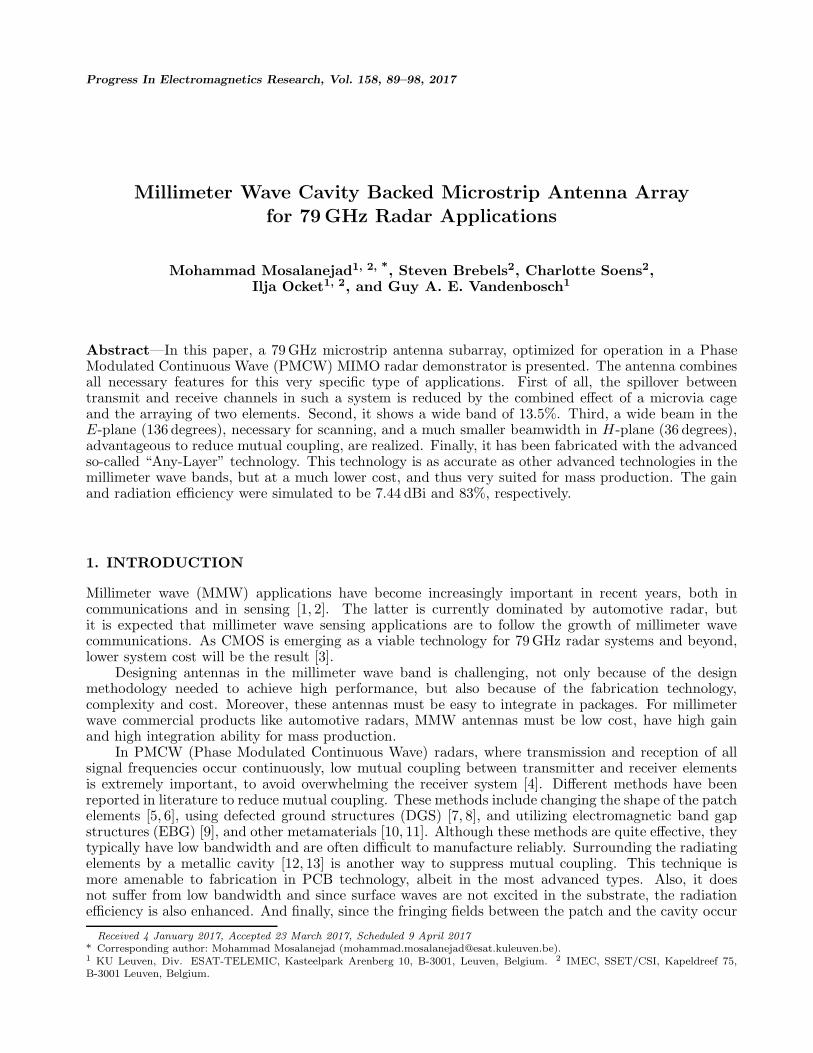
The PCB technology that is exploited is referred to as “Any-Layer Technology” [23]. The Any-LayerTechnology is an advancement of “Standard” existing HDI (High Density Interconnect) micro-viatechnology in printed circuit boards. With Any-Layer Technology, all electrical connections betweenthe individual printed circuit board layers are formed by laser-drilled micro-vias, the micro-vias arecopper filled and stacked. This gives the design community optimum design freedom as each layer orconnection on a specific layer can be connected to every other layer within the PCB stack-up. In general,conventional through holes are eliminated by this process and replaced by micro-via holes. The featuresthat go with this are quite a bit smaller than the features required for conventionally drilled, blind, orthrough holes. There is also an extensive space saving opportunity and the possibility to reduce size,layer-count and/or weight of a product. For a given product dimension, an increased routing densityis possible. A cross section of a PCB board fabricated by this technology is depicted in Fig. 1. Also,a comparison between this multilayer PCB and LTCC is made in Table 2. In fact, this technology isalmost as accurate as LTCC, but at an much lower cost. It is worth mentioning that, to the knowledgeof authors, this is the first time that this advanced multi-layer PCB technology is used in the designand fabrication of a batch of millimeter wave antennas.
The layer build-up that is actually used for the antenna fabrication is shown in Fig. 2. This build-upshows a perfect symmetry along the substrate thickness direction. 8 metal layers are used. Layers 3 and
(a) (b)
Figure 1. 3D view of Any-layer PCB cross section. The stacked microvias can be clearly seen.
Table 2. A comparison between any-layer PCB, and LTCC.
Characteristics Any-Layer PCB LTCCMinimum substrate thickness (µm) 50 50
Minimum track width (µm) 50 35Minimum micro-via diameter (µm) 70 50
Minimum clearance between tracks (µm) 50 35Cost Less More
Fabrication ease Easier Harder

92 Mosalanejad et al.
Sub6
Sub4 (Core)
Sub2
Sub1
Sub3
Sub5
Sub7
Copper 1
Copper 2 (GND1)
Copper 4 (GND2)
Copper 3
Copper 5
Copper 6
Copper 7 (GND3)
Copper 8
MicrostripStripline Patch1
Patch2 Microvias for the Cavity
Flip-Chip
60 μm (εr= 3.16, tand= 0.0125)
77 μm (εr= 3.22, tand= 0.0125)
104 μm (εr= 3.13, tand= 0.0125)
100 μm (εr= 3.34, tand= 0.0125)
104 μm (εr= 3.13, tand= 0.0125)
77 μm (εr= 3.22, tand= 0.0125)
60 μm (εr= 3.16, tand= 0.0125)
Transition
Figure 2. Layer build-up used to implement the antenna sub-array.
8 are used for the stacked patches, layers 2, 4 and 7 as ground planes, and the transition from microstripto stripline is done between layers 1 and 3. In the final radar module, layers 1, 3, 5 and 6 are also used forrouting the tracks for the different signals. The thickness of all metal layers is around 25 micrometers.Further, 7 different substrates are used. All of the laminate and prepreg materials for the substratesare of the Panasonic Megtron 6 type. Their characteristics are given in Fig. 2. The permittivity of allthese dielectrics is higher than 3. Lower permittivity materials yield a higher bandwidth, but it is hardto find and use such materials for millimeter wave applications. On top, they are very costly. Smallmicro-vias are used in substrates 2–7 to make the cavities around the patches.
3. ANTENNA SUB-ARRAY
The designed antenna sub-array is composed of 2 elements in the H-plane which are fed through acorporate feed. The elements are put in each other’s H-plane to make the beamwidth narrower in thisplane.
The narrower pattern in this plane will lead to lower mutual coupling between the Tx and Rxelements in the radar module. For this antenna sub-array, a wide band feed transition from microstrip
(a) (b)
Figure 3. (a) Microstrip to stripline transition: W1 = 0.13 mm, W2 = 0.075 mm, L2 = 0.53 mm,W3 = 0.28 mm, L3 = 0.75 mm, W4 = 0.085 mm, Lt1 = 0.1 mm, Lt2 = 0.3 mm, Lt3 = 0.1 mm,R1 = 0.185 mm, R2 = 0.11 mm, R3 = 0.2 mm. (b) Scattering parameters.
Progress In Electromagnetics Research, Vol. 158, 2017 93
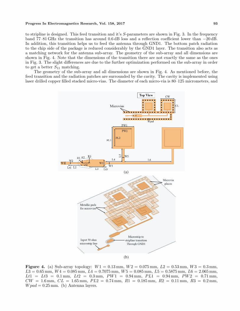
to stripline is designed. This feed transition and it’s S-parameters are shown in Fig. 3. In the frequencyband 77–81 GHz the transition has around 0.6 dB loss and a reflection coefficient lower than −20 dB.In addition, this transition helps us to feed the antenna through GND1. The bottom patch radiationto the chip side of the package is reduced considerably by the GND1 layer. The transition also acts asa matching network for the antenna sub-array. The geometry of the sub-array and all dimensions areshown in Fig. 4. Note that the dimensions of the transition there are not exactly the same as the onesin Fig. 3. The slight differences are due to the further optimization performed on the sub-array in orderto get a better S11 matching.
The geometry of the sub-array and all dimensions are shown in Fig. 4. As mentioned before, thefeed transition and the radiation patches are surrounded by the cavity. The cavity is implemented usinglaser drilled copper filled stacked micro-vias. The diameter of each micro-via is 80–125 micrometers, and
(a)
(b)
Figure 4. (a) Sub-array topology: W1 = 0.13 mm, W2 = 0.075 mm, L2 = 0.53 mm, W3 = 0.3 mm,L3 = 0.65 mm, W4 = 0.085 mm, L4 = 0.7075 mm, W5 = 0.085 mm, L5 = 0.5875 mm, L6 = 2.065 mm,Lt1 = Lt3 = 0.1 mm, Lt2 = 0.3 mm, PW1 = 0.94 mm, PL1 = 0.94 mm, PW2 = 0.71 mm,CW = 1.6 mm, CL = 1.65 mm, PL2 = 0.74 mm, R1 = 0.185 mm, R2 = 0.11 mm, R3 = 0.2 mm,Wpad = 0.25 mm. (b) Antenna layers.
94 Mosalanejad et al.
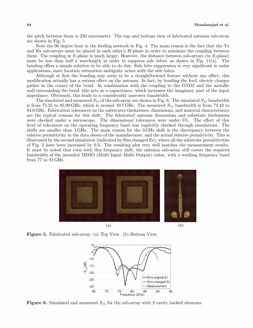
the pitch between them is 250 micrometer. The top and bottom view of fabricated antenna sub-arrayare shown in Fig. 5.
Note the 90 degree bent in the feeding network in Fig. 4. The main reason is the fact that the Txand Rx sub-arrays must be placed in each other’s H-plane in order to minimize the coupling betweenthem. The coupling in E-plane is much larger. However, the distance between sub-arrays (in E-plane)must be less than half a wavelength in order to suppress side lobes, as shown in Fig. 11(a). Thebending offers a simple solution to be able to do this. Side lobe suppression is very significant in radarapplications, since location estimation ambiguity arises with the side lobes.
Although at first the bending may seem to be a straightforward feature without any effect, thismodification actually has a serious effect on the antenna. In fact, by bending the feed, electric chargesgather in the corner of the bend. In combination with the coupling to the GND2 and the metallicwall surrounding the bend, this acts as a capacitance, which increases the imaginary part of the inputimpedance. Obviously, this leads to a considerably narrower bandwidth.
The simulated and measured S11 of the sub-array are shown in Fig. 6. The simulated S11 bandwidthis from 75.25 to 85.99 GHz, which is around 10.7 GHz. The measured S11 bandwidth is from 72.43 to84.6 GHz. Fabrication tolerances on the substrates thicknesses, dimensions, and material characteristicsare the typical reasons for this shift. The fabricated antenna dimensions and substrate thicknesseswere checked under a microscope. The dimensional tolerances were under 5%. The effect of thislevel of tolerances on the operating frequency band was explicitly checked through simulations. Theshifts are smaller than 1GHz. The main reason for the 3GHz shift is the discrepancy between therelative permittivity in the data sheets of the manufacturer, and the actual relative permittivity. This isillustrated by the second simulation (indicated by Sim-changed Er), where all the substrate permittivitiesof Fig. 2 have been increased by 0.3. The resulting plot very well matches the measurement results.It must be noted that even with this frequency shift, the antenna sub-array still covers the requiredbandwidth of the intended MIMO (Multi Input Multi Output) radar, with a working frequency bandfrom 77 to 81 GHz.
(a) (b)
Figure 5. Fabricated sub-array. (a) Top View. (b) Bottom View.
Figure 6. Simulated and measured S11 for the sub-array with 2 cavity backed elements.
Progress In Electromagnetics Research, Vol. 158, 2017 95
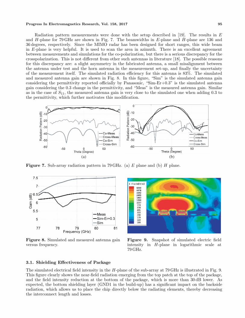
Radiation pattern measurements were done with the setup described in [19]. The results in Eand H-plane for 79 GHz are shown in Fig. 7. The beamwidths in E-plane and H-plane are 136 and36 degrees, respectively. Since the MIMO radar has been designed for short ranges, this wide beamin E-plane is very helpful. It is used to scan the area in azimuth. There is an excellent agreementbetween measurements and simulations for the co-polarization, but there is a serious discrepancy for thecrosspolarization. This is not different from other such antennas in literature [18]. The possible reasonsfor this discrepancy are: a slight asymmetry in the fabricated antenna, a small misalignment betweenthe antenna under test and the horn antenna in the measurement set-up, and finally the uncertaintyof the measurement itself. The simulated radiation efficiency for this antenna is 83%. The simulatedand measured antenna gain are shown in Fig. 8. In this figure, “Sim” is the simulated antenna gainconsidering the permittivity reported officially by Panasonic, “Sim-Er+0.3” is the simulated antennagain considering the 0.3 change in the permittivity, and “Meas” is the measured antenna gain. Similaras in the case of S11, the measured antenna gain is very close to the simulated one when adding 0.3 tothe permittivity, which further motivates this modification.
(a) (b)
Figure 7. Sub-array radiation pattern in 79 GHz. (a) E plane and (b) H plane.
Figure 8. Simulated and measured antenna gainversus frequency.
Figure 9. Snapshot of simulated electric fieldintensity in H-plane in logarithmic scale at79 GHz.
3.1. Shielding Effectiveness of Package
The simulated electrical field intensity in the H-plane of the sub-array at 79 GHz is illustrated in Fig. 9.This figure clearly shows the near-field radiation emerging from the top patch at the top of the package,and the field intensity reduction at the bottom of the package, which is more than 30 dB lower. Asexpected, the bottom shielding layer (GND1 in the build-up) has a significant impact on the backsideradiation, which allows us to place the chip directly below the radiating elements, thereby decreasingthe interconnect length and losses.
96 Mosalanejad et al.
3.2. Mutual Coupling in MIMO Radar
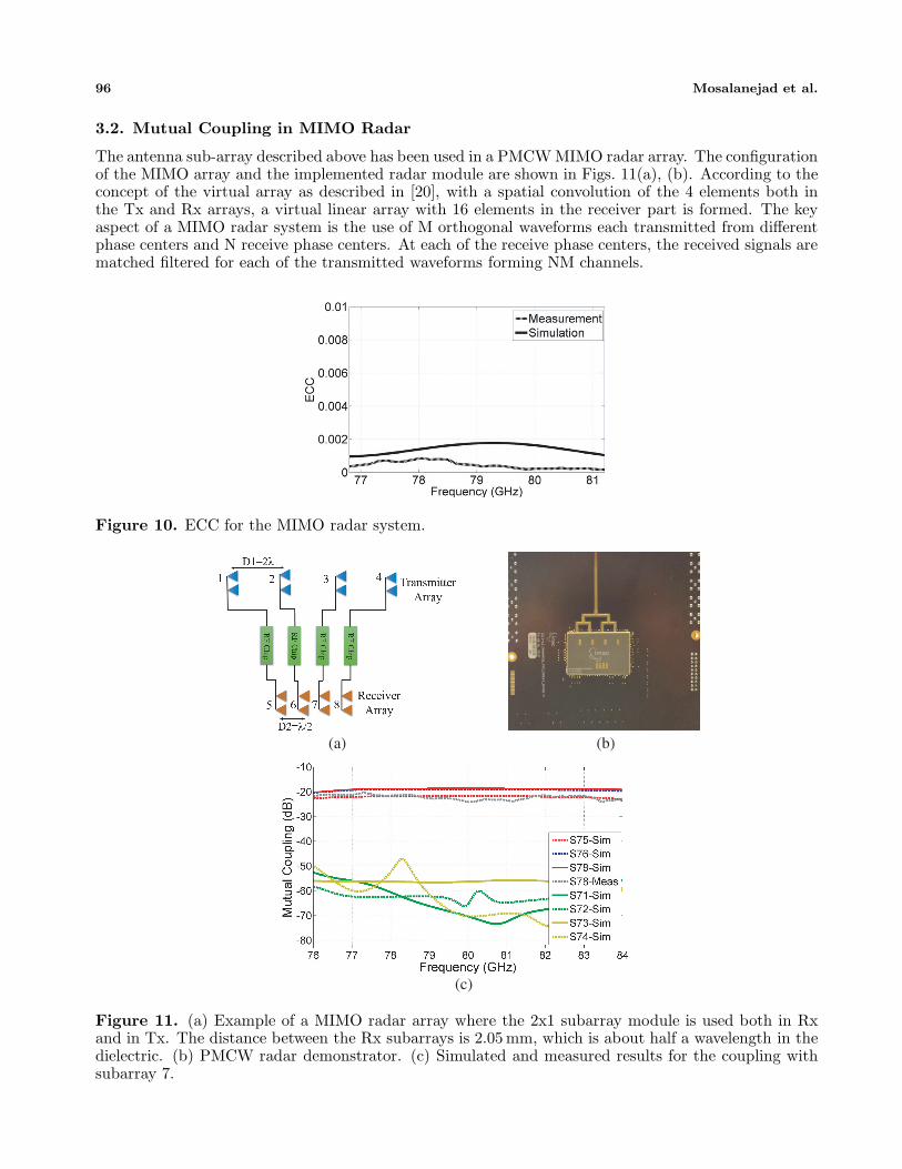
The antenna sub-array described above has been used in a PMCW MIMO radar array. The configurationof the MIMO array and the implemented radar module are shown in Figs. 11(a), (b). According to theconcept of the virtual array as described in [20], with a spatial convolution of the 4 elements both inthe Tx and Rx arrays, a virtual linear array with 16 elements in the receiver part is formed. The keyaspect of a MIMO radar system is the use of M orthogonal waveforms each transmitted from differentphase centers and N receive phase centers. At each of the receive phase centers, the received signals arematched filtered for each of the transmitted waveforms forming NM channels.
Figure 10. ECC for the MIMO radar system.
(a) (b)
(c)
Figure 11. (a) Example of a MIMO radar array where the 2x1 subarray module is used both in Rxand in Tx. The distance between the Rx subarrays is 2.05 mm, which is about half a wavelength in thedielectric. (b) PMCW radar demonstrator. (c) Simulated and measured results for the coupling withsubarray 7.
Progress In Electromagnetics Research, Vol. 158, 2017 97
It is evident that since the signal level in the Rx is low, the mutual coupling between the Tx andRx must be as low as possible. Therefore, it is crucial that the topology is designed in such a waythat mutual coupling, especially between Tx and Rx, is very low. In order to demonstrate this, themutual coupling in the MIMO array of Fig. 11(b) is studied. The simulated mutual couplings betweenelement 7 and other elements in the Rx and Tx array are shown in Fig. 11(c). These values are under−18.8 dB for Rx elements, and are under −47 dB for Tx-Rx elements. Also the level of the valuesobtained was verified by a measurement between elements 7 and 8. It must be noted that due to thefact that the mutual coupling between the receive and transmit array is extremely low (in the order of−50 dB), it is completely overwhelmed by the inaccuracies which are inevitable in present-day mm-wavemeasurement setups. For example, state-of-the-art GSG measurement probes may have a considerableparasitic radiation that disturbs the measurement far above a level of −50 dB, see [22]. Hence, themutual coupling between transmit and receive array could not be measured down to levels of −50 dB.
The Envelope Correlation Coefficient (ECC) is another criterion to assess the isolation of multipleantennas in MIMO systems. Using the definition in [21], this parameter is plotted in Fig. 10. Consideringthat for MIMO systems, an ECC lower than 0.3 is excellent, it is seen that the ECC for this antenna isextremely low in the 76–82 GHz band.
As mentioned before, the Any-Layer technology provides us with microvias that are quite a bitsmaller than through hole vias. Moreover, they can be placed more closely to form the cavity aroundthe patches. This feature provides two main benefits for the MIMO radar. First, this leads to moremitigation of surface waves and mutual coupling. Second, since the microvias are smaller and their padsare very narrow, the antenna elements in Rx can be placed at a distance very close to half a wavelength,which avoids side grating lobes.
4. CONCLUSION
In this paper, a new cavity backed stacked patch antenna topology for 79 GHz MIMO radar applicationsis introduced. The antenna is fabricated with a low cost high resolution advanced Any-Layer PCBtechnology. Reflection coefficient and radiation pattern measurement and simulation results show agood agreement. The antenna topology has a very wide beamwidth in both E plane (more than 135degrees) and H plane. These wide beam widths are necessary for short range radars. The impedancebandwidth is more than 13.5%, which completely fulfills the requirements of radar applications in the79 GHz band. In contrast to topologies already described in literature, the wide bandwidth is achievedwith small elements (smaller than half a wavelength) and without embedding air cavities into thebuild-up, which enhances both the complexity and cost. In addition, due to a novel and widebandfeed transition from microstrip to stripline, the radiation to the chip side has been reduced by morethan 30 dB. Furthermore, thanks to the small and high resolution microvias provided by the Any-Layertechnology, a low mutual coupling below −18.8 dB is reached over the whole radar bandwidth, withoutusing extra structures like EBG or DGS.
REFERENCES
1. Cui, B., C. Wang, and X.-W. Sun, “Microstrip Array Double-Antenna (MADA) technology appliedin millimeter wave compact radar front-end,” Progress In Electromagnetics Research, Vol. 66, 125–136, 2006.
2. Camblor-Diaz, R., S. Ver-Hoeye, C. Vazquez-Antuna, G. R. Hotopan, M. Fernandez-Garcia, andF. Las Heras Andres, “Sub-millimeter wave frequency scanning 8 × 1 antenna array,” Progress InElectromagnetics Research, Vol. 132, 215–232, 2012.
3. Hasch, J., E. Topak, R. Schnabel, T. Zwick, R. Weigel, and C. Waldschmidt, “Millimeter-wavetechnology for automotive radar sensors in the 77 GHz frequency band,” IEEE Trans. Microw.Theory Techn., Vol. 60, No. 3, Part 2, 845–860, 2012.
4. Guermandi, D., Q. Shi, A. Medra, T. Murata, W. Van Thillo, A. Bourdoux, P. Wambacq, andV. Giannini, “A 79 GHz binary phase-modulated continuous-wave radar transceiver with TX-to-RX

98 Mosalanejad et al.
spillover cancellation in 28 nm CMOS,” 2015 IEEE International Solid-State Circuits Conference(ISSCC), 1–3, 2015.
5. Wong, K. W., L. Chiu, and Q. Xue, “A 2-D van atta array using star-shaped antenna elements,”IEEE Trans. Antennas Propag., Vol. 55, No. 4, 1204–1206, 2007.
6. Yousefzadeh, N., C. Ghobadi, and M. Kamyab, “Consideration of mutual coupling in a microstrippatch array using fractal elements,” Progress In Electromagnetics Research, Vol. 66, 41–49, 2006.
7. Farahbakhsh, A., M. Mosalanejad, Gh. Moradi, and Sh. Mohanna, “Using polygonal defect in groundstructure to reduce mutual coupling in microstrip array antenna,” Journal of Electromagnetic Wavesand Applications, Vol. 28, No. 2, 194–201, 2014.
8. Ghosh, C. K., B. Mandal, and S. K. Parui, “Mutual coupling reduction of a dual frequency microstripantenna array by using U-shaped DGS and inverted U-shaped microstrip resonator,” Progress InElectromagnetics Research C, Vol. 48, 61–68, 2014.
9. Islam, M. T. and M. S. Alam, “Compact EBG structure for alleviating mutual coupling betweenpatch antenna array elements,” Progress In Electromagnetics Research, Vol. 137, 425–438, 2013.
10. Yang, X. M., X. G. Liu, X. Y. Zhou, and T. J. Cui, “Reduction of mutual coupling between closelypacked patch antennas using waveguided metamaterials,” IEEE Antennas Wireless Propag. Lett.,Vol. 11, 389–391, 2012.
11. Qamar, Z. and H. C. Park, “Compact waveguided metamaterials for suppression of mutual couplingin microstrip array,” Progress In Electromagnetics Research, Vol. 149, 183–192, 2014.
12. Li, Y. and K.-M. Luk, “60-GHz substrate integrated waveguide fed cavity-backed aperture-coupledmicrostrip patch antenna arrays,” IEEE Trans. Antennas Propag., Vol. 63, No. 3, 1075–1085, 2015.
13. Ou Yang, J., S. Bo, J. Zhang, and F. Yang, “A low-profile unidirectional cavity-backed log-periodicslot antenna,” Progress In Electromagnetics Research, Vol. 119, 423–433, 2011.
14. Kam, D., D. Liu, A. Natarajan, S. Reynolds, H. Chen, and B. A. Floyd, “LTCC packages withembedded phased-array antennas for 60 GHz communications,” IEEE Antennas Wireless Propag.Lett., Vol. 21, No. 3, 142–144, 2011.
15. Pazin, L. and Y. Leviatan, “A compact 60-GHz tapered slot antenna printed on LCP substrate forWPAN applications,” IEEE Antennas Wireless Propag. Lett., Vol. 9, 272–275, 2010.
16. Brebels, S., Ch. Soens, W. De Raedt, and G. A. E. Vandenbosch, “Compact LTCC antenna packagefor 60 GHz wireless transmission of uncompressed video,” IEEE MTT-S International MicrowaveSymposium Digest, 1–4, 2011.
17. Liu, D., J. A. G. Akkermans, H. Chen, and B. Floyd, “Packages with integrated 60-GHz aperture-coupled patch antennas,” IEEE Trans. Antennas Propag., Vol. 59, No. 10, 3607–3616, 2011.
18. Enayati, A., G. A. E. Vandenbosch, and W. De Raedt, “Millimeter-wave horn-type antenna-in-package solution fabricated in a teflon-based multi-layer PCB technology,” IEEE Trans. AntennasPropag., Vol. 61, No. 4, 1581–1590, 2013.
19. Mosalanejad, M., S. Brebels, I. Ocket, V. Volski, C. Soens, and G. A. E. Vandenbosch, “A completemeasurement system for integrated antennas at millimeter wavelengths,” 9th European Conferenceon Antennas and Propagation (EuCAP), 1–5, 2015.
20. Haimovich, A., R. Blum, and L. Cimini, “MIMO radar with widely separated antennas,” IEEESignal Process. Mag., Vol. 25, No. 1, 116–129, 2008.
21. Blanch, S., J. Romeu, and I. Corbella, “Exact representation of antenna system diversityperformance from input parameter description,” Electronics Letters, Vol. 39, No. 9, 705–707, 2003.
22. Mohammadpour-Aghdam, K., S. Brebels, A. Enayati, R. Faraji-Dana, G. Vandenbosch, andW. DeRaedt, “RF probe influence study in millimeterwave antenna pattern measurements,”International Journal of RF and Microwave Computer-aided Engineering, Vol. 21, No. 4, 413–420,2011.
23. Aspocomp PCB technology, Keilaranta, Finland, Website: “https://www.aspocomp.com”.


![Planar Microstrip-To-Waveguide Transition in Millimeter-Wave Band · 2013-03-12 · that of ordinary transitions of a waveguide and a coaxial cable [11]. The probe transition connects](https://img.dokumen.tips/doc/110x75/5e930936dfd03a310714bb10/planar-microstrip-to-waveguide-transition-in-millimeter-wave-band-2013-03-12-that.jpg)


![Ku-Band High Performance Monopulse Microstrip …concern especially in high frequency millimeter wave applications [19]. In this article, a high gain low sidelobe monopulse microstrip](https://img.dokumen.tips/doc/110x75/5f01ce827e708231d4012136/ku-band-high-performance-monopulse-microstrip-concern-especially-in-high-frequency.jpg)