Embed Size (px)
Citation preview

Page 1
Copyright © 2017 Avnet, Inc. AVNET, “Reach Further,” and the AV logo are registered trademarks of Avnet, Inc. All other brands are the property of their respective owners.
LIT# 5274-MicroZed-Carrier-Design-Guide-rev-1-5-V1
MicroZed™ Carrier Design Guide Version 1.5

Page 2
Document Control
Document Version: 1.5
Document Date: 4/14/2014
Prior Version History
Version Date Comment
1.0 02/05/2014 Initial Release
1.1 02/07/2014 Added CARRIER BOARD PCB GUIDELINES section
1.2 02/10/2014 Updated MICROZED CONNECTORS section
1.3 03/07/2014 Added Connector Shock and Vibration Specifications
1.4 04/01/2014 - Updated multiple tables
- Added note under PUDC_B section.
- Updated Pair Matching and Length Tuning section
- Updated Carrier Boards PCB Guidelines section
- Updated Connector Land and Alignment section
- Corrected information related to CARRIER_SRST#
- Updated XADC section
1.5 04/14/2014 Added Power Architecture and Sequencing Diagram

Page 3
Contents
1 INTRODUCTION ..................................................................................................... 5
1.1 Glossary .................................................................................................................................... 5
1.2 Additional Documentation ......................................................................................................... 5
2 MICROZED OPTIONS ............................................................................................ 6
2.1 PL Resources ............................................................................................................................ 6
2.2 PL I/O ........................................................................................................................................ 6
2.3 Thermal ..................................................................................................................................... 6
3 MICROZED INTERFACES ...................................................................................... 7
3.1 PS .............................................................................................................................................. 8
3.1.1 MIO .................................................................................................................................... 8
3.1.2 Control ............................................................................................................................... 9
3.2 PL IO SIGNALS....................................................................................................................... 10
3.3 Analog ..................................................................................................................................... 11
3.4 JTAG ....................................................................................................................................... 13
3.5 Configuration ........................................................................................................................... 14
3.5.1 PUDC_B .......................................................................................................................... 14
3.5.2 DONE .............................................................................................................................. 14
3.5.3 INIT_B.............................................................................................................................. 14
3.5.4 PROGRAM_B.................................................................................................................. 15
3.6 Ethernet MAC ID ..................................................................................................................... 15
4 POWER AND RESET ............................................................................................ 16
4.1 General Power Requirements ................................................................................................. 16
4.2 Power Estimation of PL using XPE ......................................................................................... 16
4.3 Power Sourcing Options ......................................................................................................... 16
4.4 Proper Sequencing.................................................................................................................. 17
4.5 Power Handling of PL I/O Banks ............................................................................................ 17
4.6 Proper Handling of VBAT ........................................................................................................ 17
4.7 Proper Handling of XADC Power ............................................................................................ 18
4.8 Need for Additional Bypass Capacitors .................................................................................. 18
5 CARRIER BOARD PCB GUIDELINES ................................................................. 19
5.1 Suggested Requirements for Optimum Carrier Card Performance ........................................ 19
5.1.1 Global Target Impedances (Unless otherwise noted) ..................................................... 19
5.1.2 Pair Matching and Length Tuning ................................................................................... 19
5.1.3 Routing Considerations for Additional DDR Modules (PL via JX Connectors) ............... 20
5.2 Routing 1Gb/s Ethernet Port Through the PL ......................................................................... 21
6 MICROZED CONNECTORS ................................................................................. 22

Page 4
6.1 Connector Description and Selection ...................................................................................... 22
6.1.1 Connector Shock and Vibration Specifications ............................................................... 23
6.2 MicroHeader Pinouts ............................................................................................................... 24
6.3 Connector Land and Alignment............................................................................................... 26
7 MECHANICAL CONSIDERATIONS ..................................................................... 27
7.1 Form Factor ............................................................................................................................. 28
7.2 Thermal Considerations .......................................................................................................... 30
8 GETTING HELP AND SUPPORT ......................................................................... 31

Page 5
1 INTRODUCTION
This document provides information for designing a custom system carrier card for MicroZed. It includes reference schematics for the external circuitry required to implement the various MicroZed peripheral functions. It also explains how to extend the supported buses and how to add additional peripherals and expansion slots.
1.1 Glossary
Term Definition
MIO Multiplexed Input Output – the dedicated I/O available on the PS
PL Programmable Logic
POR Power On Reset
PS Processing System
1.2 Additional Documentation Additional information and documentation on Xilinx’s Zynq®-7000 All Programmable SoCs can be found at www.xilinx.com/zynq. Additional information and documentation on MicroZed (with IO Carrier Card) can be found at www.microzed.org.

Page 6
2 MICROZED OPTIONS MicroZed comes in both 7010 and 7020 versions. Additionally, each version is offered populated with Commercial temperature grade (0° C to 70° C) or Industrial temperature Grade (-40° C to 85° C).
2.1 PL Resources The resource comparison between the 7010 and 7020 Zynq devices can be seen in Xilinx document XMP087.
2.2 PL I/O The 7020 version connects 15 additional I/O to the MicroHeaders in a third PL Bank (Bank 13). The MicroHeaders provide for independent Vcco pins for this bank, which provides for additional voltage flexibility. Please note the PL IO Bank power rails (Vccio_34, Vccio_35, and Vccio_13 [7020 version only]) must be powered from a MicroZed carrier card via JX1 and JX2 if used.
2.3 Thermal As the 7020 version has significantly more internal PL resources than the 7010, it is possible that extra care will need to be taken in the thermal management.

Page 7
3 MICROZED INTERFACES A Carrier Card may utilize several Zynq interfaces on the MicroZed. A table showing the Signals, Pin Count, and Zynq source is shown below. The Zynq Interfaces discussed in this section are:
– PS
– PL
– Analog
– JTAG
– Configuration
MicroHeader #1 (JX1) MicroHeader #2 (JX2)
Signal Name Source Pin Count
Signal Name Source Pin Count
PL
Bank 34 I/Os (except for PUDC_B)
Zynq Bank 34 49
PL
Bank 35 I/Os Zynq Bank 35 50
JT
AG
TMS_0 Zynq Bank 0 5 P
S PS Pmod
MIO[0,9-15] Zynq Bank 500 8
TDI_0 Zynq Bank 0
TCK_0 Zynq Bank 0
C Init_B_0 Zynq Bank 0 1
TDO_0 Zynq Bank 0
Pow
er
Vccio_EN Module/Carrier 1
Carrier_SRST# Carrier PG_MODULE Module/Carrier 1
Analo
g VP_0 Zynq Bank 0 4 Vin Carrier 5
VN_0 Zynq Bank 0 GND Carrier 23
DXP_0 Zynq Bank 0 VCCO_13 Carrier 1
DXN_0 Zynq Bank 0 VCCO_35 Carrier 3
C
PUDC_B / IO Zynq Bank 34 2 Bank 13 pins Bank 13 ** 7
DONE Zynq Bank 0 TOTAL 100
Pow
er
PWR_Enable Carrier 1
Vin Carrier 4
GND Carrier 23
VCCO_34 Carrier 3
VBATT Carrier 1
Bank 13 pins Bank 13 ** 8
TOTAL 100
Table 1 – MicroHeader Pinout
** 7020 device only

Page 8
3.1 PS
3.1.1 MIO Eight PS MIOs (0, 9-15) are shared between the Pmod connector on-board the MicroZed and the JX2 MicroHeader. When plugged into a Carrier, it is intended that the PS MIO Pmod on the MicroZed would not be used.
SoC Pin # MIO MicroZed Net JX2 Pin #
JX2 Pin #
MicroZed Net MIO SoC Pin #
Bank 500, E8 13 PMOD_D0 1 2 PMOD_D1 10 Bank 500, E9
Bank 500, C6 11 PMOD_D2 3 4 PMOD_D3 12 Bank 500, D9
Bank 500, E6 0 PMOD_D4 5 6 PMOD_D5 9 Bank 500, B5
Bank 500, C5 14 PMOD_D6 7 8 PMOD_D7 15 Bank 500, C8
Table 2 – JX2 PS MIO Connections
Multiple Zynq PS peripherals will map to these eight pins. A new hardware platform must be designed to enable the desired peripheral.
Zynq PS Peripheral MIOs Used
Dual Quad SPI (8 bit) 0, 9-13
SDIO (SD1) 10-15
SPI (SPI1) 10-13 or 10-15 (up to 3 devices)
UART (UART0) 10-11 or 14-15
I2C (I2C0) 10-11 or 14-15
I2C (I2C1) 12-13
CAN (CAN0) 10-11 or 14-15
CAN (CAN1) 12-13
System Watchdog Timer (SWD) 14-15
Processor JTAG (PJTAG) 10-13
Trace Clock & Control 12-13
Trace Data (1/2/4 bits) 14 or 14-15 or 14-15, 10-11
GPIO 0, 9-15
Table 3 – Zynq PS Peripheral Mapping to Carrier

Page 9
3.1.2 Control MicroZed routes two system control signals to the MicroHeaders.
Function Signal Name MicroHeader
Connection Subsection Zynq pin
External System Reset
CARRIER_SRST# JX1.6 PS (MIO Bank 501) B10
External Power-
on-Reset PG_MODULE JX2.11 PS (MIO Bank 500) C7
Table 4 – System Control Signals
External system reset, labeled CARRIER_SRST#, is connected to Zynq signal PS_SRST_B. External system reset allows the user to reset all of the functional logic within the device without disturbing the debug environment. For example, the previous break points set by the user remain valid after the external system reset. While CARRIER_SRST# is held Low, all PS I/Os are held in 3-state. Due to security concerns, system reset erases all memory content within the PS, including the OCM. The PL is also reset in system reset. System reset does not re-sample the boot mode strapping pins.
CARRIER_SRST# is an active-low signal. Asserting this signal asserts Zynq signal PS_SRST_B through an open-drain buffer (NC7WZ07FHX). When not asserted, this signal can either be driven high or left to float.
If this pin is not used in the system, it can be left floating since it is pulled up on the MicroZed (R63).
Note: This signal cannot be asserted while the boot ROM is executing following a POR reset. If PS_SRST# is asserted while the boot ROM is running through a POR reset sequence it will trigger a lock-down event preventing the boot ROM from completing. To recover from lockdown the device either needs to be power cycled or PS_POR_B needs to be asserted.
The Zynq PS supports an external power-on reset signal. The power-on reset is the master reset of the entire chip. This signal resets every register in the device capable of being reset. On MicroZed this signal, labeled PG_MODULE, is connected to the power good output of the final stage of the power regulation circuitry. These power supplies have open drain outputs that pull this signal low until the output voltage is valid. A carrier card should also wire-OR to this net and not release it until the carrier card power is also good. Other IC’s on MicroZed are reset by this signal as well.
The signal can also be actively pulled low to initiate a power-on reset.
To stall Zynq boot-up, this signal should be held low. No other signal (SRST, PROGRAM_B, INIT_B) is capable of doing this as in other FPGA architectures.

Page 10
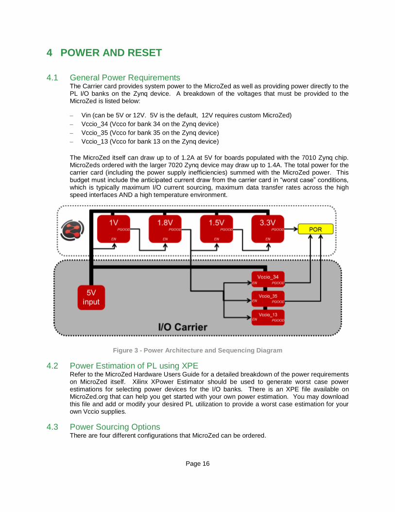
3.2 PL IO SIGNALS MicroZed connects 50 I/Os from both Bank 34 and Bank 35. Additionally, the 7020 version adds another 15 I/O from Bank 13. Each of these banks has independent power pins for Vcco on the MicroHeaders. When flexibility in voltage standard is needed, each bank can be powered from a separate regulator. When cost is a concern, then all PL I/O banks can be tied to the same Vcco regulator.
Figure 1 shows a diagram of the banking and MicroHeader distribution is shown below.
Figure 1 – MicroZed I/O Banking
A detailed discussion of the PL I/Os is available in Section 2.8.2 of the MicroZed Hardware User Guide. This includes details on clock-capable pins, trace length matching, differential routing, and DQ byte groups for a possible PL DDR3 MIG-based design on a Carrier.

Page 11
3.3 Analog The Zynq XADC pins are connected through the MicroZed MicroHeaders. For details of how this might be connected, see the MicroZed I/O Carrier Card User Guide and Schematics. Also, refer to Chapter 30 of the Zynq TRM and UG480.
Carrier Net Name
MicroHeader Connection
Zynq AP SOC Connection
Description
XADC_VP_0_P JX1, pin 97 Bank 0, K9 XADC dedicated differential analog input
XADC_VP_0_N JX1, pin 99 Bank 0, L10
XADC_DXP_0_P JX1, pin 98 Bank 0, M9 Temperature-sensing
diode pins XADC_DXN_0_N JX1, pin 100 Bank 0, M10
XADC_AD0_P JX2, pin 17 Bank 35, C20 Differential auxiliary
analog inputs XADC_AD0_N JX2, pin 19 Bank 35, B20
XADC_AD1_P JX2, pin 23 Bank 35, E17
XADC_AD1_N JX2, pin 25 Bank 35, D18
XADC_AD2_P JX2, pin 36 Bank 35, M19
XADC_AD2_N JX2, pin 38 Bank 35, M20
XADC_AD3_P JX2, pin 35 Bank 35, L19
XADC_AD3_N JX2, pin 37 Bank 35, L20
XADC_AD4_P JX2, pin 54 Bank 35, J18
XADC_AD4_N JX2, pin 56 Bank 35, H18
XADC_AD5_P JX2, pin 68 Bank 35, J20
XADC_AD5_N JX2, pin 70 Bank 35, H20
XADC_AD6_P JX2, pin 73 Bank 35, K14
XADC_AD6_N JX2, pin 75 Bank 35, J14
XADC_AD7_P JX2, pin 82 Bank 35, L14
XADC_AD7_N JX2, pin 84 Bank 35, L15
XADC_AD8_P JX2, pin 18 Bank 35, B19
XADC_AD8_N JX2, pin 20 Bank 35, A20
XADC_AD9_P JX2, pin 29 Bank 35, E18
XADC_AD9_N JX2, pin 31 Bank 35, E19
XADC_AD10_P JX2, pin 41 Bank 35, M17
XADC_AD10_N JX2, pin 43 Bank 35, M18
XADC_AD11_P JX2, pin 42 Bank 35, K19
XADC_AD11_N JX2, pin 44 Bank 35, J19
XADC_AD12_P JX2, pin 62 Bank 35, F19
XADC_AD12_N JX2, pin 64 Bank 35, F20
XADC_AD13_P JX2, pin 67 Bank 35, G19
XADC_AD13_N JX2, pin 69 Bank 35, G20
XADC_AD14_P JX2, pin 81 Bank 35, N15
XADC_AD14_N JX2, pin 83 Bank 35, N16
XADC_AD15_P JX2, pin 88 Bank 35, K16
XADC_AD15_N JX2, pin 90 Bank 35, J16
Table 5 - XADC Pinout

Page 12
On MicroZed, the XADC internal reference voltage is selected (VREFP and VREFN shorted AGND).
VCCADC on the MicroZed is the on-board 1.8V filtered through a ferrite board, with 0.1uF and 0.47uF bypass caps.
If you plan to make use of the XADC on your Carrier, it is suggested that you place anti-aliasing filters close to JX1/2, similar to what is seen on the Microzed I/O Carrier Card.
Figure 2 – Anti-Aliasing Filters for XADC Inputs (see UG480)
– The 100Ω filtering resistors and 1000pF capacitor should be placed within 500 mils of the associated FPGA pins.
– Use 4X spacing on the traces.
– Single ended impedance is 50Ω and differential is 100Ω.
– All paired signals should be routed to within 50mils of each other.
– All interface signals should be routed to within 100mils of each other.
– Anti-aliasing filters should be placed as close to the MicroHeader as possible.
Be aware that the analog signal level is maximum 1Vpp, with an absolute maximum of 1.8V. When used as Analog inputs, the recommended voltage level is given in the Zynq datasheet. The excerpt below is taken from DS187, v1.11. Since VCCADC on MicroZed is tied to 1.8V, the absolute maximum on these inputs is 1.8V when used as analog channels. The maximum voltage on the auxiliary channels when used as digital channels is governed by the Bank 35 Vcco and IOSTANDARD.
To MicroHeader From Analog Front End

Page 13
Table 6 – DS187 v1.11 Table 97
When the XADC is not used, DXP/N, VP/N pins should be connected to GND. All the auxiliary analog inputs become digital I/O. Examples of this mode are seen on the FMC and Breakout Carrier Cards.
3.4 JTAG Since the MicroZed can be used standalone, the JTAG signals are connected on the MicroZed to a Xilinx PC4-style JTAG socket. The four dedicated JTAG signals are also routed to the MicroHeaders. A Carrier Card MAY choose to utilize these JTAG signals. If so, then the JTAG socket on the MicroZed should NOT be used.
When connecting additional JTAG devices in-line with the MicroZed, be sure that TCK and TMS are properly buffered. For example, if you wanted to Device XYZ into the JTAG chain, you would design your Carrier Card with a PC4-socket, with TMS and TCK buffers after the socket. The buffered TMS and TCK would route to both Device XYZ and the MicroHeaders. Then the TDI/TDO connections would daisy-chain.
PC4 TDI JX1.4
JX1.3 Device XYZ TDI
Device XYZ TDO PC4 TDO
This process has been validated on the MicroZed FMC Carrier Card. If the Carrier Card has no need to access the JTAG signals, then these can be left unconnected. The JTAG socket on the MicroZed may then be used with the MicroZed plugged into the Carrier.
SoC Pin # MicroZed Net JX1
Pin #
JX1
Pin # MicroZed Net SoC Pin #
Bank 0, F9 JTAG_TCK 1 2 JTAG_TMS Bank 0, J6
Bank 0, F6 JTAG_TDO 3 4 JTAG_TDI Bank 0, G6
Table 7 – JX1 Connections

Page 14
3.5 Configuration
3.5.1 PUDC_B This signal is MicroZed net name JX1_LVDS_2_P. This signal has a resistor jumper option on MicroZed to pull-up to Vcco_34 or pull-down to GND. The default is to pull it up via a 1K-ohm resistor, which disables the pull-ups during configuration.
This signal is routed to the Carrier. The default pull-up can be over-ridden with a stronger pull-down if pull-ups during configuration are desired.
Function Signal Name MicroHeader
Connection Subsection Zynq pin
Pull-ups During
Configuration JX1_LVDS_2_P JX1.17 PL (Bank 34) U13
Table 8 – PUDC_B
NOTE: Due to PUDC_B functionality on JX1_LVDS_2_P, the JX1_LVDS_2_P and JX1_LVDS_2_N pair are not suitable for use as a differential pair.
3.5.2 DONE The DONE signal is pulled-up on MicroZed via a 240-ohm resistor, which also enables LED D2. The DONE signal is also routed to the Carrier and can be used as a control input to signal when the PL is DONE configuring.
Function Signal Name MicroHeader Connection
Subsection Zynq pin
PL Config DONE FPGA_DONE JX1.8 Bank 0 R11
Table 9 – DONE
3.5.3 INIT_B INIT_B is pulled-up via 4.7K-ohm on the MicroZed. If not needed as a controls signal on the Carrier, this can be left disconnected.
Function Signal Name MicroHeader Connection
Subsection Zynq pin
PL Initialization INIT# JX2.9 Bank 0 R10
Table 10 – INIT_B

Page 15
3.5.4 PROGRAM_B PROGRAM_B is pulled-up via 4.7K-ohm on the MicroZed. For Zynq applications, it is not typical that a system would use this signal. On Rev C and later MicroZed, this signal is not connected to the Carrier.
Function Signal Name MicroHeader
Connection Subsection Zynq pin
PL Program PROGRAM# none Bank 0 L6
Table 11 – INIT_B
3.6 Ethernet MAC ID From the factory, MicroZed does not store a MAC ID for the Ethernet. A designer could choose to implement this in the MicroZed Flash using their own MAC ID assignments.
A MAC ID could also be implemented using a dedicated MAC ID EEPROM, similar to what can be seen on the MicroZed FMC Carrier.
Page 16
4 POWER AND RESET
4.1 General Power Requirements The Carrier card provides system power to the MicroZed as well as providing power directly to the PL I/O banks on the Zynq device. A breakdown of the voltages that must be provided to the MicroZed is listed below:
– Vin (can be 5V or 12V. 5V is the default, 12V requires custom MicroZed)
– Vccio_34 (Vcco for bank 34 on the Zynq device)
– Vccio_35 (Vcco for bank 35 on the Zynq device)
– Vccio_13 (Vcco for bank 13 on the Zynq device)
The MicroZed itself can draw up to of 1.2A at 5V for boards populated with the 7010 Zynq chip. MicroZeds ordered with the larger 7020 Zynq device may draw up to 1.4A. The total power for the carrier card (including the power supply inefficiencies) summed with the MicroZed power. This budget must include the anticipated current draw from the carrier card in “worst case” conditions, which is typically maximum I/O current sourcing, maximum data transfer rates across the high speed interfaces AND a high temperature environment.
Figure 3 - Power Architecture and Sequencing Diagram
4.2 Power Estimation of PL using XPE Refer to the MicroZed Hardware Users Guide for a detailed breakdown of the power requirements on MicroZed itself. Xilinx XPower Estimator should be used to generate worst case power estimations for selecting power devices for the I/O banks. There is an XPE file available on MicroZed.org that can help you get started with your own power estimation. You may download this file and add or modify your desired PL utilization to provide a worst case estimation for your own Vccio supplies.
4.3 Power Sourcing Options There are four different configurations that MicroZed can be ordered.

Page 17
– 7010 Zynq-7000 5V input (default configuration)
– 7020 Zynq-7000 12V input (custom BOM)
– 7010 Zynq-7000 12V input (custom BOM)
– 7020 Zynq-7000 5V input (custom BOM)
12V MicroZed adds a 12V to 5V regulator to provide power to the USB bus. By default this bus is tied to Vin, which is why a BOM modification is required to use a 12V input. Powering MicroZed off of a 12V input without modification can result in damage to any USB peripherals connected to the board.
5V is the default option for MicroZed. There is an additional cost associated with modifying MicroZed to support a 12V source. Unless there is a compelling reason to use 12V (an FMC interface for example) it is recommended to use 5V as your input source. FMC is a standard interface that is widely used in FPGA development, MicroZed was designed to be able to support 12V for this reason.
4.4 Proper Sequencing All three Vccio banks that receive power from the carrier can be independent, or tied together depending on the specific design needs. To maintain proper start up sequencing, these Vccio supplies should be enabled by the VCCIO_EN signal tied to JX2 pin 10. Note that this enable signal is the PGOOD for the 1.8V supply on MicroZed. It is vital to ensure that the enable threshold for the regulators chosen is compatible with a 1.8V signal. If 1.8V is not high enough to reliably enable the device, an external circuit must be used to boost this voltage. An example of such a circuit can be found in the schematic for the FMC Carrier card.
To enable power to the MicroZed, PWR_EN must be pulled high. PWR_EN is tied to JX1 pin 5 and is pulled up to Vin on the MicroZed. To shut down power to the MicroZed, PWR_EN and VCCIO_EN should be pulled low. VCCIO_EN should be pulled low first to maintain proper shutdown sequencing. See the Power Architecture and Sequencing Diagram for more detail.
4.5 Power Handling of PL I/O Banks For designing the power supplies for the PL I/O banks the XPower Estimator file available at www.microzed.org under documentation. This file can be modified based on how you plan to use your I/O. The power estimation results can then be used to budget for the power that will be needed by the MicroZed PL I/O banks. This current should be added to the carrier power estimate when designing your power system.
4.6 Proper Handling of VBAT If battery backup is required, VBATT must be tied to a 1.8V battery source through JX1 pin 7. Note that MicroZed by default ties VBATT directly to 1.8V Vccaux. If using VBATT as a battery backup, R12 on MicroZed must be removed.

Page 18
4.7 Proper Handling of XADC Power The XADC interface operates from a 1.8V supply voltage with a 1.25V reference. Be sure to design your interface with these values in mind. Do not exceed 1.8V on the XADC inputs. For additional information on designing with this interface please refer to Xilinx Application Note XAPP554 – XADC Layout Guidelines.
4.8 Need for Additional Bypass Capacitors Bulk and decoupling/bypass capacitance is provided on MicroZed. Additional capacitance should be added to the user designed carrier as recommended by the device manufacturers for each interface.

Page 19
5 CARRIER BOARD PCB GUIDELINES The majority of the MicroZed PL signals are routed to the JX connectors to facilitate user design flexibility and application development. Differential pairs and single ended signals are available for custom carrier card designs. All high speed routing must follow the specific device manufacturers’ recommendations for routing, impedance, trace length and layout guidelines. This is applicable to any high speed or low noise signals such as DDR RAM, Ethernet PHY, PMODs, XADC or USB extensions. The design engineer must be diligent in these areas to ensure intended data rates and performance.
The specific design requirements for a user application will ultimately drive the trace length, trace spacing, signaling topology (differential or single ended) and impedance requirements. This variability cannot be accounted for and data throughput, signal integrity and overall performance will vary based on the design approach.
In all circumstances the design of a user carrier board, the following documents should be consulted and adhered to: MicroZed User Guide, the associated Avnet I/O Carrier Card, FMC Card or Breakout board User Guide, and Xilinx’s UG430. These documents provide critical insight into how the Avnet products were designed.
For general guidelines on how to achieve the performance of the Avnet I/O Carrier Card designs, Avnet Engineering Services suggests the following design requirements be adhered to.
5.1 Suggested Requirements for Optimum Carrier Card Performance
5.1.1 Global Target Impedances (Unless otherwise noted)
– 100Ω differential impedance
– 50Ω single ended impedance
– USB: 45Ω single ended, 90Ω differential
– DDR: 40Ω single ended, 80Ω differential
5.1.2 Pair Matching and Length Tuning
– Use 4x spacing between pairs
– All signals should be routed using stripline or microstrip techniques to ensure the signals meet 6.1.1.
– Length tune all signal pairs to within 10 mils within each pair (P to N)
– Length tune all signal pairs to within 250 mils pair-to-pair (depending on transfer rates)
Page 20
Figure 4: Avnet MicroZed Board Topology
5.1.3 Routing Considerations for Additional DDR Modules (PL via JX Connectors) – LPDDR2, DDR2, and DDR3 should be selected based on MIG tool for a Zynq processor.
– Use the MIG tool pin-out information to route from the JX1 and JX2 connectors on the carrier board.
– Place memory IC (or ICs), pending topology and memory density, as close as possible to the JX1 and JX2 microheaders for maximum data transfer rates and to minimize long trace lengths.
– Follow specific memory manufacturer’s routing guidelines, trace impedance requirements and termination topology. The MicroZed uses a 40Ω ohm single ended and 80Ω differential trace impedance for the specific DDR3 with a 3X spacing between pairs, matching the memory manufacturer’s recommendations.
– Routing, impedance and termination requirements will vary depending on the memory manufacture, the quantity of DDR ICs, the topology and the desired data throughput performance.
– As a general rule for high speed memory, Avnet adheres and recommends memory trace lengths to be less than 5000 mil in total length.
– All memory signals should be length tuned according to total propagation delay or “flight time” as recommended by Xilinx and the chosen memory manufacturer.

Page 21
– Avnet recommends routing all memory signals on inner layers only, within 10mils of each other pair to pair, less than 50mils for a byte-lane associated to each DQS, and all memory signals to be within 100 mils of each other.
5.2 Routing 1Gb/s Ethernet Port Through the PL – Using Vivado IP integrator or ISE Core Generator, develop a PMAC interface for the Zynq
PL.
– All Giga-bit signals should be routed stripline using micro-vias between the appropriate layers.
– Use 4x spacing between pairs.
– Single pair (P and N) should be length tuned to within 25 mils of each other (P to N) at 100Ω differential impedance, with no more than two transitions (vias) for these signals.
– All Data, clock and control signals (RX, TX, MDx) should be routed at 50Ω impedance and not exceed the PHY manufacturers’ recommended length requirements.
– All interface signals should be routed to within 250mils of each other.
– If RGMII interface is used, the related VCCO must supply 1.8V or 2.5V to support fast slew.
– The Ethernet PHY must be compatible with VCCO levels used.

Page 22
6 MICROZED CONNECTORS Each MicroZed SoM features two 100-pin MicroHeaders (JX1 and JX2) that allow for connection to customer carrier cards. The MicroHeaders route I/O signals and power between MicroZed and a custom carrier card.
6.1 Connector Description and Selection The MicroHeaders used on MicroZed are FCI 0.8mm BergStak® 100-position Dual Row, BTB Vertical Receptacles (61082-101400LF). These receptacles mate with any of the FCI 0.8mm BergStak® 100-position Dual Row BTB Vertical Plugs (61083-10x400LF) to provide variable stack heights of 5mm, 6mm, 7mm or 8mm. See table below for additional detail.
Custom MicroZeds can be ordered with specific plugs while custom carrier cards can be populated with specific receptacles allowing system designers to choose optimal stacking heights (5mm – 16mm in 1mm increments) for their particular application. See table below for additional detail.
Figure 5 – FCI BergStak Mating Options
Page 23
Additionally, each MicroHeader pin can carry 500mA of current and can support data rates up to 8Gbps. More information on FCI’s BergStak connectors can be found at www.fciconnect.com/bergstak.
Avnet will keep the following FCI part numbers in Table 12 in stock to assist prototype build of custom carrier cards. See www.em.avnet.com/avnetsomconnectors for more details.
61082-10140xLF* 61083-10140xLF*
61082-10240xLF* 61083-10240xLF*
61082-10340xLF* 61083-10340xLF*
61083-10440xLF*
* “x” can be 0, 2 or 9 depending on packaging.
Table 12 - FCI BERGSTAK Connectors
Avnet will keep the following FCI part numbers in Table 12 in stock to assist prototype build of custom carrier cards. See www.em.avnet.com/avnetsomconnectors for more details.
6.1.1 Connector Shock and Vibration Specifications
Shock: EIA-364-27, Test Condition A Accelerated velocity ----- 490 m/s2 (50G). Waveform ------------------ half-sine shock pulse. Duration -------------------- 11 mSec. Velocity change ----------- 11.3 feet per second Number of cycles --------- 18
Vibration: EIA-364-28 Test Condition V, Letter D Frequency ------------------ 50 to 2000 Hz Power spectral Density -------- 0.1 g2/Hz Overall rms g ---------------- 11.95 Duration --------------------- 1 1/2 hours in each of three mutually perpendicular axes (4 1/2 hours total).
Page 24
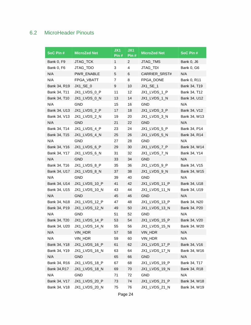
6.2 MicroHeader Pinouts
SoC Pin # MicroZed Net JX1
Pin #
JX1
Pin # MicroZed Net SoC Pin #
Bank 0, F9 JTAG_TCK 1 2 JTAG_TMS Bank 0, J6
Bank 0, F6 JTAG_TDO 3 4 JTAG_TDI Bank 0, G6
N/A PWR_ENABLE 5 6 CARRIER_SRST# N/A
N/A FPGA_VBATT 7 8 FPGA_DONE Bank 0, R11
Bank 34, R19 JX1_SE_0 9 10 JX1_SE_1 Bank 34, T19
Bank 34, T11 JX1_LVDS_0_P 11 12 JX1_LVDS_1_P Bank 34, T12
Bank 34, T10 JX1_LVDS_0_N 13 14 JX1_LVDS_1_N Bank 34, U12
N/A GND 15 16 GND N/A
Bank 34, U13 JX1_LVDS_2_P 17 18 JX1_LVDS_3_P Bank 34, V12
Bank 34, V13 JX1_LVDS_2_N 19 20 JX1_LVDS_3_N Bank 34, W13
N/A GND 21 22 GND N/A
Bank 34, T14 JX1_LVDS_4_P 23 24 JX1_LVDS_5_P Bank 34, P14
Bank 34, T15 JX1_LVDS_4_N 25 26 JX1_LVDS_5_N Bank 34, R14
N/A GND 27 28 GND N/A
Bank 34, Y16 JX1_LVDS_6_P 29 30 JX1_LVDS_7_P Bank 34, W14
Bank 34, Y17 JX1_LVDS_6_N 31 32 JX1_LVDS_7_N Bank 34, Y14
N/A GND 33 34 GND N/A
Bank 34, T16 JX1_LVDS_8_P 35 36 JX1_LVDS_9_P Bank 34, V15
Bank 34, U17 JX1_LVDS_8_N 37 38 JX1_LVDS_9_N Bank 34, W15
N/A GND 39 40 GND N/A
Bank 34, U14 JX1_LVDS_10_P 41 42 JX1_LVDS_11_P Bank 34, U18
Bank 34, U15 JX1_LVDS_10_N 43 44 JX1_LVDS_11_N Bank 34, U19
N/A GND 45 46 GND N/A
Bank 34, N18 JX1_LVDS_12_P 47 48 JX1_LVDS_13_P Bank 34, N20
Bank 34, P19 JX1_LVDS_12_N 49 50 JX1_LVDS_13_N Bank 34, P20
N/A GND 51 52 GND N/A
Bank 34, T20 JX1_LVDS_14_P 53 54 JX1_LVDS_15_P Bank 34, V20
Bank 34, U20 JX1_LVDS_14_N 55 56 JX1_LVDS_15_N Bank 34, W20
N/A VIN_HDR 57 58 VIN_HDR N/A
N/A VIN_HDR 59 60 VIN_HDR N/A
Bank 34, Y18 JX1_LVDS_16_P 61 62 JX1_LVDS_17_P Bank 34, V16
Bank 34, Y19 JX1_LVDS_16_N 63 64 JX1_LVDS_17_N Bank 34, W16
N/A GND 65 66 GND N/A
Bank 34, R16 JX1_LVDS_18_P 67 68 JX1_LVDS_19_P Bank 34, T17
Bank 34,R17 JX1_LVDS_18_N 69 70 JX1_LVDS_19_N Bank 34, R18
N/A GND 71 72 GND N/A
Bank 34, V17 JX1_LVDS_20_P 73 74 JX1_LVDS_21_P Bank 34, W18
Bank 34, V18 JX1_LVDS_20_N 75 76 JX1_LVDS_21_N Bank 34, W19

Page 25
N/A GND 77 78 VCCO_34 N/A
N/A VCCO_34 79 80 VCCO_34 N/A
Bank 34, N17 JX1_LVDS_22_P 81 82 JX1_LVDS_23_P Bank 34, P15
Bank 34, P18 JX1_LVDS_22_N 83 84 JX1_LVDS_23_N Bank 34, P16
N/A GND 85 86 GND N/A
Bank 13, U7 BANK13_LVDS_0_P 87 88 BANK13_LVDS_1_P Bank 13, T9
Bank 13, V7 BANK13_LVDS_0_N 89 90 BANK13_LVDS_1_N Bank 13, U10
Bank 13, V8 BANK13_LVDS_2_P 91 92 BANK13_LVDS_3_P Bank 13, T5
Bank 13, W8 BANK13_LVDS_2_N 93 94 BANK13_LVDS_3_N Bank 13, U5
N/A GND 95 96 GND N/A
Bank 0, K9 VP_0_P 97 98 DXP_0_P Bank 0, M9
Bank 0, L10 VN_0_N 99 100 DXN_0_N Bank 0, M10
Table 13 – JX1 Connections
SoC Pin # MicroZed Net JX2
Pin #
JX2
Pin # MicroZed Net SoC Pin #
Bank 500, E8 PMOD_D0 1 2 PMOD_D1 Bank 500, E9
Bank 500, C6 PMOD_D2 3 4 PMOD_D3 Bank 500, D9
Bank 500, E6 PMOD_D4 5 6 PMOD_D5 Bank 500, B5
Bank 500, C5 PMOD_D6 7 8 PMOD_D7 Bank 500, C8
Bank 0, R10 INIT# 9 10 VCCIO_EN N/A
Bank 500, C7 PG_MODULE 11 12 VIN_HDR N/A
Bank 35, G14 JX2_SE_0 13 14 JX2_SE_1 Bank 35, J15
N/A GND 15 16 GND N/A
Bank 35, C20 JX2_LVDS_0_P 17 18 JX2_LVDS_1_P Bank 35, B19
Bank 35, B20 JX2_LVDS_0_N 19 20 JX2_LVDS_1_N Bank 35, A20
N/A GND 21 22 GND N/A
Bank 35, E17 JX2_LVDS_2_P 23 24 JX2_LVDS_3_P Bank 35, D19
Bank 35, D18 JX2_LVDS_2_N 25 26 JX2_LVDS_3_N Bank 35, D20
N/A GND 27 28 GND N/A
Bank 35, E18 JX2_LVDS_4_P 29 30 JX2_LVDS_5_P Bank 35, F16
Bank 35, E19 JX2_LVDS_4_N 31 32 JX2_LVDS_5_N Bank 35, F17
N/A GND 33 34 GND N/A
Bank 35, L19 JX2_LVDS_6_P 35 36 JX2_LVDS_7_P Bank 35, M19
Bank 35, L20 JX2_LVDS_6_N 37 38 JX2_LVDS_7_N Bank 35, M20
N/A GND 39 40 GND N/A
Bank 35, M17 JX2_LVDS_8_P 41 42 JX2_LVDS_9_P Bank 35, K19
Bank 35, M18 JX2_LVDS_8_N 43 44 JX2_LVDS_9_N Bank 35, J19
N/A GND 45 46 GND N/A
Bank 35, L16 JX2_LVDS_10_P 47 48 JX2_LVDS_11_P Bank 35, K17
Bank 35, L17 JX2_LVDS_10_N 49 50 JX2_LVDS_11_N Bank 35, K18

Page 26
N/A GND 51 52 GND N/A
Bank 35, H16 JX2_LVDS_12_P 53 54 JX2_LVDS_13_P Bank 35, J18
Bank 35, H17 JX2_LVDS_12_N 55 56 JX2_LVDS_13_N Bank 35, H18
N/A VIN_HDR 57 58 VIN_HDR N/A
N/A VIN_HDR 59 60 VIN_HDR N/A
Bank 35, G17 JX2_LVDS_14_P 61 62 JX2_LVDS_15_P Bank 35, F19
Bank 35, G18 JX2_LVDS_14_N 63 64 JX2_LVDS_15_N Bank 35, F20
N/A GND 65 66 GND N/A
Bank 35, G19 JX2_LVDS_16_P 67 68 JX2_LVDS_17_P Bank 35, J20
Bank 35, G20 JX2_LVDS_16_N 69 70 JX2_LVDS_17_N Bank 35, H20
N/A GND 71 72 GND N/A
Bank 35, K14 JX2_LVDS_18_P 73 74 JX2_LVDS_19_P Bank 35, H15
Bank 35, J14 JX2_LVDS_18_N 75 76 JX2_LVDS_19_N Bank 35, G15
N/A GND 77 78 VCCO_35 N/A
N/A VCCO_35 79 80 VCCO_35 N/A
Bank 35, N15 JX2_LVDS_20_P 81 82 JX2_LVDS_21_P Bank 35,L14
Bank 35, N16 JX2_LVDS_20_N 83 84 JX2_LVDS_21_N Bank 35,L15
N/A GND 85 86 GND N/A
Bank 35, M14 JX2_LVDS_22_P 87 88 JX2_LVDS_23_P Bank 35, K16
Bank 35, M15 JX2_LVDS_22_N 89 90 JX2_LVDS_23_N Bank 35, J16
N/A GND 91 92 GND N/A
Bank 13, Y12 BANK13_LVDS_4_P 93 94 BANK13_LVDS_5_P Bank 13, V11
Bank 13, Y13 BANK13_LVDS_4_N 95 96 BANK13_LVDS_5_N Bank 13, V10
Bank 13, V6 BANK13_LVDS_6_P 97 98 VCCO_13 N/A
Bank 13, W6 BANK13_LVDS_6_N 99 100 BANK13_SE_0 Bank 13, V5
Table 14 – JX2 Connections
6.3 Connector Land and Alignment It is extremely important that MicroZed carrier card designers ensure that the MicroHeaders have the proper land patterns and that the connectors are aligned correctly. The land pattern is featured in the Mechanical Considerations section of this document. Connector alignment is ensured if the alignment pin holes in the PCB connector pattern are in the correct positions and if the holes are drilled to the proper size and tolerance by the PCB fabricator.
Additionally, Avnet has developed an Altium-based MicroZed schematic symbol and PCB footprint. This is available on the MicroZed Documentation page under the Layout section.

Page 27
7 MECHANICAL CONSIDERATIONS MicroZed measures 2.25” x 4.00” (57.15 mm x 101.6 mm). Custom carrier cards would have to be large enough to support the dimension shown below.
MicroZed comes with four grounded and plated mounting holes in each of the four corners of the board. The diameter of each mounting hole is 0.125” (3.175mm). Assuming the standard 5mm board-to-board spacing between MicroZed and the carrier card, spacers (i.e. Harwin R30-3000502 with M3x5mm metal screw and M3 x 1mm metal nut) can be added to mechanically strengthen the attachment of MicroZed to the carrier card. Metal standoffs provide an additional heat dissipation path for any possible heat buildup on the ground layer.
MicroZed comes with two un-plated mounting holes near the Zynq device. The diameter of each mounting hole is 0.093” (2.362mm). These can be used to secure thermal relief elements like fans or a heat spreader. M2 diameter screws, spacers and nuts can be used on the mounting holes. See the following figures for more detail.
Figure 6 – MicroZed Side Vertical Dimensions (Side)
Figure 7- MicroZed Max Vertical Dimensions (Front)

Page 28
7.1 Form Factor
Figure 8 - Mechanical Layout of I/O Carrier Card MicroHeader Connectors and Mounting Holes

Page 29
Figure 9 - MicroZed Bottom-side Mechanical Dimensions (inches)

Page 30
7.2 Thermal Considerations Thermal relief is an important design factor in each MicroZed-based system design. A detailed thermal analysis should be performed for each specific application of MicroZed and a customer designed carrier card. In support of this, MicroZed has many design features to help dissipate heat from a system level.
The first feature is the fan header (JP4 – labeled “FAN”). This header provides two ground connections and one connection to the VIN voltage (5v by default but 12V compatible). This allows a fan to be added to any MicroZed-based system. For maximum heat dissipation, any system airflow should pass parallel to the surface of the Zynq.
Related to the fan header are two mounting holes (MTG[3:4]) located next to the Zynq device. This allows for a fan, heat sink or fan and heatsink combination to be added to the MicroZed. System engineers may decide to mount a heat spreader here in extreme situations.
Lastly, the four mounting holes on the four corners of MicroZed are electrically connected to a heavier ground plane. With the additional vias added to MicroZed, system designers may choose to attach MicroZed to their customer carrier card using metal standoff providing another path for heat dissipation.
In some instances adding a passive heat sink with appropriate thermal bonding material to the Zynq may be sufficient to dissipate any extra heat. The Zynq CLG400 package used on MicroZed measures 17mm by 17mm. For maximum heat transfer, passive heat sinks attached to the Zynq device should cover the entire area. Suggested devices below serve as a starting point for basic heat dissipation needs.
Manufacturer Part Number L x W X H (mm) Thermal Resistance (°C/W)
AavidThermalloy 10-53190245-C2-HSG 19 x 19 x 24.5 6.5
AavidThermalloy 10-53190145-C1-R0G 19 x 19 x 14.5 12
AavidThermalloy 10-53190095-C1-R0G 19 x 19 x 9.5 22
CTS APF19-19-06CB 19 x 19 x 6.3 7.1*
CTS APF19-19-10CB 19 x 19 x 9.5 5.3*
CTS APF19-19-13CB 19 x 19 x 12.7 4.0*
Table 15 – MicroZed Heatsink Options
*@200LFM

Page 31
8 GETTING HELP AND SUPPORT If additional support is required, Avnet has many avenues to search depending on your needs.
For general question regarding MicroZed, MicroZed Carrier Card or accessories, please visit our website at http://www.microzed.org. Here you can find documentation, technical specifications, videos and tutorials, reference designs and other support.
Detailed questions regarding MicroZed hardware design, software application development, using Xilinx tools, training and other topics can be posted on the MicroZed Support Forums at http://www.microzed.org/forums/zed-english-forum. Avnet’s technical support team monitors the forum during normal business hours in both English and Mandarin. Typical response time is less than 48 hours.
Those interested in customer-specific options on MicroZed can send inquiries to [email protected].
Avnet’s Embedded Software Store addresses the need for software in the embedded architecture development space. The goal of this store is to provide a market place for engineers to easily purchase software components for given hardware architectures. Support for the Xilinx Zynq AP SoC includes Board Support Packages, Middleware, Operating Systems and various tools
The Embedded Software and Services Group (ESSG) of Avnet Embedded offers a suite of software services that optimize the entire embedded software stack. Flexible end-to-end solutions enhance operating systems, middleware, application layers and cloud solutions based on the embedded system needs. More information can be found at http://www.em.avnet.com/en-us/services/Pages/Software-Solutions.aspx.