Embed Size (px)
Citation preview

Hewlett Packard
Microwave Probing
HP 84000 RFIC On-Wafer TestMerging Two Worlds of Test
Jim Bossaller 6/2/97SWTW San DiegoHewlett Packard
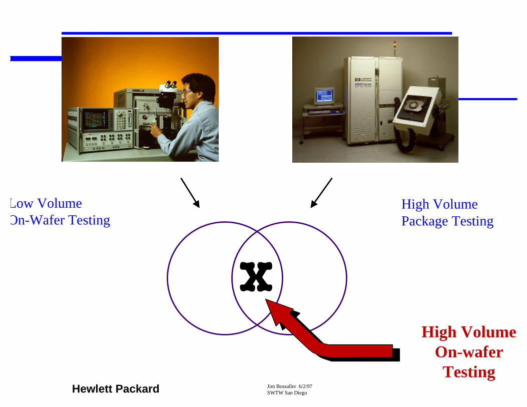
Low VolumeOn-Wafer Testing
High VolumePackage Testing
High VolumeOn-waferTesting

Jim Bossaller 6/2/97SWTW San DiegoHewlett Packard
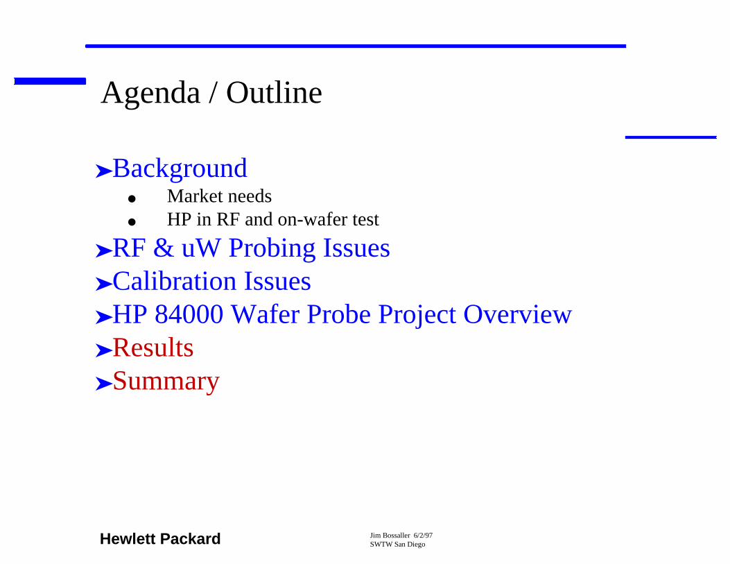
Agenda / Outline
➤Background● Market needs● HP in RF and on-wafer test
➤RF & uW Probing Issues➤Calibration Issues➤HP 84000 Wafer Probe Project Overview➤Results➤Summary
Jim Bossaller 6/2/97SWTW San DiegoHewlett Packard
Agenda / Outline
➤Background● Market needs● HP in RF and on-wafer test
➤RF & uW Probing Issues➤Calibration Issues➤HP 84000 Wafer Probe Project Overview➤Results➤Summary

Jim Bossaller 6/2/97SWTW San DiegoHewlett Packard
Background:Market / Technology drivers for on-wafer test systemsfor the late 1990’s
➤Wireless Communications RFIC’s● Cellular Telephones● Cordless Telephones● Direct Broadcast Satellite TV
➤Implications● High Volumes● Low Frequency (<3GHz)● Silicon (not just GaAs anymore)● Higher levels of IC integration● Commercial not Military applications
Jim Bossaller 6/2/97SWTW San DiegoHewlett Packard
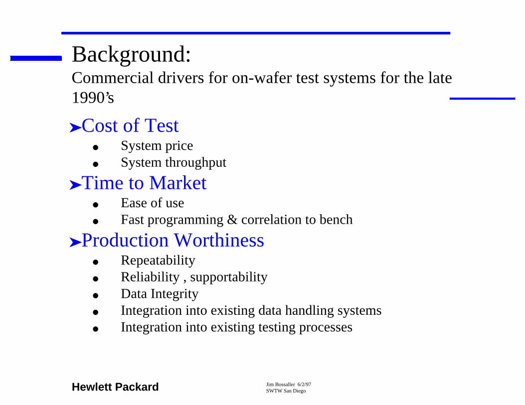
Background:Commercial drivers for on-wafer test systems for the late1990’s
➤Cost of Test● System price● System throughput
➤Time to Market● Ease of use● Fast programming & correlation to bench
➤Production Worthiness● Repeatability● Reliability , supportability● Data Integrity● Integration into existing data handling systems● Integration into existing testing processes

Jim Bossaller 6/2/97SWTW San DiegoHewlett Packard
Background:HP in RF & Microwave on-wafer testing
➤>20 years of experience➤RF and microwave systems 0 to 26, 50, 65 and
110 GHz● Hundreds of systems installed worldwide
➤HP has had many years to learn the "art" of on-wafer testing at high frequencies
● Signal integrity● Calibration errors, standards, and de-embedding● Touchdown repeatability and accuracy● Test system accuracy / stability / dynamic range

Jim Bossaller 6/2/97SWTW San DiegoHewlett Packard
Background:HP 84000 in production RFIC testing
HW & SW Test Plans Fixturing HandlerIntegration
Support
The Total Solution for your RFIC testingsince 1994
Jim Bossaller 6/2/97SWTW San DiegoHewlett Packard
Agenda / Outline
➤Background● Market needs● HP in RF and on-wafer test
➤RF & uW Probing Issues➤Calibration Issues➤HP 84000 Wafer Probe Project Overview➤Results➤Summary

Jim Bossaller 6/2/97SWTW San DiegoHewlett Packard
It is easy to evaluate the particular situation and determine if the cost oftesting and removing bad die before packaging is less costly than the costof packaging bad die.
RF & Microwave Probing IssuesTest: On wafer or package? Simple economics!

Jim Bossaller 6/2/97SWTW San DiegoHewlett Packard
RF & Microwave Probing IssuesIC Design for RF Testability
Item:
Must have DC ground return pad on eachside of the chip to be probed
Must tie all grounds together on chip toeliminate common lead inductance
Must use "standard" RF signal footprint forpads (e.g. G-S-G or G-S)
Must have RF ground adjacent to RF signalpads
RF Pad spaced logically around the chipperimeter
Reason:
Prevents bias oscillations
Prevents common lead inductance-induced RFdegradation
Allows common use of probes in all RFapplications
Good RF launch onto the chip
Allows signal isolation and mechanical spacing forrelatively large probes
Jim Bossaller 6/2/97SWTW San DiegoHewlett Packard
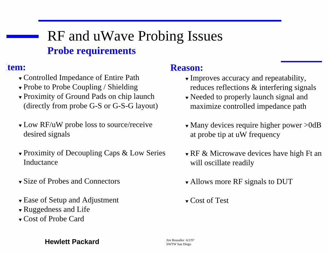
Reason:▼ Improves accuracy and repeatability,
reduces reflections & interfering signals▼ Needed to properly launch signal and
maximize controlled impedance path
▼ Many devices require higher power >0dBmat probe tip at uW frequency
▼ RF & Microwave devices have high Ft anwill oscillate readily
▼ Allows more RF signals to DUT
▼ Cost of Test
RF and uWave Probing IssuesProbe requirements
Item:▼ Controlled Impedance of Entire Path▼ Probe to Probe Coupling / Shielding▼ Proximity of Ground Pads on chip launch
(directly from probe G-S or G-S-G layout)
▼ Low RF/uW probe loss to source/receivedesired signals
▼ Proximity of Decoupling Caps & Low SeriesInductance
▼ Size of Probes and Connectors
▼ Ease of Setup and Adjustment▼ Ruggedness and Life▼ Cost of Probe Card

Jim Bossaller 6/2/97SWTW San DiegoHewlett Packard
Agenda / Outline
➤Background● Market needs● HP in RF and on-wafer test
➤RF & uW Probing Issues➤Calibration Issues➤HP 84000 Wafer Probe Project Overview➤Results➤Summary

Jim Bossaller 6/2/97SWTW San DiegoHewlett Packard
RF and uWave ProbingCalibration
▼ Calibration and de-embedding process
● Calibrate to connectorized calibration plane with traceablestandards + verification device
● Calibrate at probe tips using on wafer standards● Calculate an error model for the delta which includes adapter,
cables and probes● Use de-embedding model for all measurements including power
and noise

Jim Bossaller 6/2/97SWTW San DiegoHewlett Packard
RF and uWave ProbingCalibration
▼Why use a two level approach to calibration atthe probe tips?
● Calibration of power and noise is easily calibrated at theconnectorized plane and is readily de-embedded to the probe tip
● Can use LRM calibration which doesn’t require a difficult tocreate "open" standard at probe tip
● Changing a probe card only requires a simple on wafer LRM calto collect error model before resuming testing
● Performance of the test system to a connectorized calibrationplane is the basis of measurement integrity and performanceverification of the test system

Jim Bossaller 6/2/97SWTW San DiegoHewlett Packard
Agenda / Outline
➤Background● Market needs● HP in RF and on-wafer test
➤RF & uW Probing Issues➤Calibration Issues➤HP 84000 Wafer Probe Project Overview➤Results➤Summary
Jim Bossaller 6/2/97SWTW San DiegoHewlett Packard
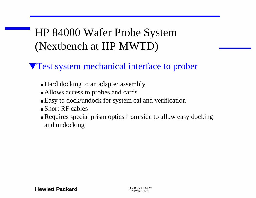
HP 84000 Wafer Probe System(Nextbench at HP MWTD)
▼Test system mechanical interface to prober
● Hard docking to an adapter assembly● Allows access to probes and cards● Easy to dock/undock for system cal and verification● Short RF cables● Requires special prism optics from side to allow easy docking
and undocking

Jim Bossaller 6/2/97SWTW San DiegoHewlett Packard
▼Photos and Drawings
● Picture of testhead docked to wafer prober● Picture of prober docking adapter● Picture of probe card with GGB probes (Picoprobe)● Picture of membrane probe● Picture of probe tips● RF measurement de-embedding test result comparison
HP 84000 Wafer Probe Project(Nextbench at HP MWTD)

Jim Bossaller 6/2/97SWTW San DiegoHewlett Packard
HP 84000 Wafer Probe Project (Nextbenchat HP MWTD)
▼Next steps on HP84000 next bench project
● Integrate industry standard wafer mapping software● Integrate industry standard wafer prober control● Integrate industry standard data analysis● Integration of the above with HP84000 operator and developer
UI, calibration and PVST (Performance Verification and SelfTest)
● System performance specifications finalized
End result is complete production worthy, highvolume, on wafer test system
Jim Bossaller 6/2/97SWTW San DiegoHewlett Packard
Agenda / Outline
➤Background● Market needs● HP in RF and on-wafer test
➤RF & uW Probing Issues➤Calibration Issues➤HP 84000 Wafer Probe Project Overview➤Results➤Summary

Jim Bossaller 6/2/97SWTW San DiegoHewlett Packard
HP 84000 Series RFIC Test System
Jim Bossaller 6/2/97SWTW San DiegoHewlett Packard
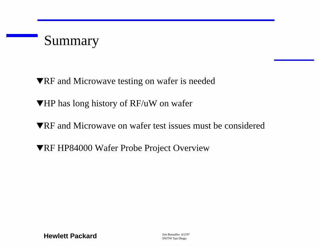
Summary
▼RF and Microwave testing on wafer is needed
▼HP has long history of RF/uW on wafer
▼RF and Microwave on wafer test issues must be considered
▼RF HP84000 Wafer Probe Project Overview