Embed Size (px)
Citation preview
Microwave Inter-Connections and Switching by means of Carbon Nano-tubes Review article
Giorgio De Angelis1, Andrea Lucibello1, Emanuela Proietti1, Romolo Marcelli1,* Daniele Pochesci2, Giancarlo Bartolucci3, Mircea Dragoman4 and Daniela Dragoman5 1 CNR-IMM Roma, Italy 2 Thales Alenia Space, Italy 3 University of Roma “Tor Vergata”, Italy 4 National Institute for Research and Development in Micro-Systems, Romania 5 University of Bucharest, Physics Faculty, Romania *Corresponding author E-mail: [email protected] Received 8 July, 2011; Accepted 30 July, 2011
Abstract In this work, carbon nanotube (CNT) based interconnections and switches will be reviewed, discussing the possibility to use nanotubes as potential building blocks for signal routing in microwave networks. In particular, theoretical design of coplanar waveguide (CPW), micro‐strip single‐pole‐single‐throw (SPST) and single‐pole‐double‐throw (SPDT) devices has been performed to predict the electrical performances of CNT‐based RF switching configurations. Actually, by using the semiconductor‐conductor transition obtained by properly biasing the CNTs, an isolation better than 30 dB can be obtained between the ON and OFF states of the switch for very wide bandwidth applications. This happens owing to the shape deformation and consequent change in the band‐gap due to the external pressure caused by the electric field. State‐of‐art for other switching techniques based on CNTs and their use for RF nano‐interconnections is also discussed, together with current issues in measurement techniques. Keywords Carbon Nanotubes, Microwaves, Switching, Band‐Gap Engineering.
1. Introduction Carbon Nano‐Tubes (CNT) are wires of pure carbon having nanometer diameters and lengths up to many microns. A single‐walled carbon nanotube (SWNT) may be thought as a single atomic layer thick sheet of graphene rolled in cylinder‐like structure. Multi‐walled carbon nanotubes (MWNT) consist of several concentric nanotube shells. The electronic properties of the graphene strongly influence those of the carbon nanotubes. Actually, a two dimensional graphene sheet is a zero‐gap semiconductor. The dispersion at the Dirac points is circular, independent of direction. Electrons or holes can flow in all directions and there is no bandgap. When it is rolled up along certain directions (such as an armchair) a metallic CNT is obtained, whereas other directions can give a semiconducting CNT. When graphene is rolled up to make the nanotube, the direction along the axis of the nanotube is the preferential
Nanomater. nanotechnol., 2011, Vol. 1, No. 1, 64-7764 www.intechweb.orgwww.intechopen.com
Nanomater. nanotechnol., 2011, Vol. 1, No. 1, 64-77

one. By properly biasing with an electric field the CNT, a transition between two possible states (semiconductor and conductor) could be driven because of the mechanical deformation induced by the pressure exerted by the electrical force due to the bias voltage. Since such a transition can change the conductivity up to six orders of magnitude, CNTs are ideal candidates for molecular electronics technologies. In particular, CNTs have been recently considered as suitable of high frequency signal processing applications by using active and passive devices [1][2][3]. Single‐Pole‐Single‐Throw (SPST), Single‐Pole‐Double‐Throw (SPDT) configurations can take advantage from the reversible metal‐semiconductor transitions, as proposed for devices based on Single‐Walled CNT [1]. The decrease in the microwave loss attenuation for Double‐Walled CNTs integrated in dielectric membrane supported devices up to 65 GHz has been also studied in [1]. Actually, considering the jump of several orders of magnitude in the change of the CNTs conductivity as it is reported in [1][4], they can be used in complex architectures for signal routing, like matrices, with several implications in terms of ground and space applications, where the miniaturization is a vital requirement. In this work, theoretical design of coplanar waveguide (CPW) and micro‐strip SPST and SPDT devices has been performed to evaluate the potential electrical performances of CNT‐based RF configurations as building blocks for signal routing in Microwave networks. Nano‐wires properly metalized could be used as an alternative solution to the previously described applications. Actually, they could be oriented under the influence of a magnetic or an electric field, contributing to opening or closing electrical contacts, and realizing the same function for high frequency switching. In this case, the mechanical properties of the structure are also involved, which can be at the nano‐scale level required by nano electro‐mechanical systems (NEMS) or at a micro‐scale if they are grouped to form a beam. The nano‐ or micro‐structure has to be properly tailored to be integrated in an electrically matched system. 2. Carbon nano‐fiber and nano‐tube interconnections Microwave switching by means of the change of the electronic properties of a device when it is subjected to an external bias is the usual way to get ON and OFF states in diodes or transistors. Fully passive devices like MEMS switches get the same result by means of the electrostatic actuation of cantilevers or double clamped beams, and they are competing at the micro‐scale with classical pin diodes because of clear advantages in terms of losses, bandwidth and distortion free capabilities [5][6]. Even power handling is now under consideration for the utilization of RF MEMS switches in redundancy, matrix
and phase shifter configurations. All of the above devices and subsystems are well established, or they are currently considered as solutions in those architectures where down‐sizing with respect to the micro‐scale is prohibitive for inherent limitations of the used technologies. RF nano‐electronics is currently evolving because of the increased necessity for miniaturization and nano‐scale interconnections [7]. Depending on the desired application, carbon nano‐fibers or nano‐tubes are investigated for properties to be used in several environments, encompassing structural and electronic systems. The ability to grow and to pattern nano‐tubes is particularly important for developing nano‐scale interconnections in 3D systems, taking advantages from vertical vias and planar very low loss connections. Carbon nano‐fibers (CNF) and carbon nano‐tubes (CNT), have both mechanical and electrical properties which make them interesting for applications in microelectronics, as well as in microwave devices. CNT have desirable properties of high stiffness, high aspect ratio (lengths up to mm for diameters spanning from 1 to 100 nm), high thermal stability, high thermal conductivity (up to 6000 W/K/m) and large current carrying capacity (more than 109A/cm2 in metallic CNT). CNF have a more disordered morphology compared to CNT. While the nano‐fiber is a stack of graphitic layers with a cone morphology defined by a non‐zero cone angle, an ideal nano‐tube is a cylinder. However, nano‐fibers have the advantage to grow at lower temperatures than nano‐tubes, using plasma‐enhanced chemical vapour deposition (PECVD) [10]. CNF are also considerably cheaper than CNT. CNF and CNT have recently been proposed as a replacement material to copper for vertical and horizontal interconnects in integrated circuits [10],[11],[12]. Moreover, Fujitsu Laboratories have also demonstrated the selective growth of vertical CNT used as flip‐chip bumps, which have a high thermal conductivity, for high power dissipation [20]. For these applications, DC electrical characterizations of CNT and CNF have been extensively reported. However, the work to study the potential of CNT and CNF for interconnects at microwave frequencies and for microwave devices is just beginning. Notably, the first experimental characterizations at high‐frequencies were performed on SWCNT [15][16][17][18] and CNF [14]. The approach used was the measurement of scattering parameters from two‐port networks enclosing horizontal CNF/CNT. Then a de‐embedding
Nanomater. nanotechnol., 2011, Vol. 1, No. 1, 64-7765 www.intechweb.orgwww.intechopen.com
technique was used to remove parasitic effects and extract the S parameters of the CNF/CNT and the results were fitted to equivalent RLC models. Besides, a phenomenological analysis, reported in [13], has been used to predict that the intrinsic electrical cut‐off frequency of SWCNT would be in the terahertz range, which would open up the possibility of extremely fast devices. An example is reported in [19], which presents a microwave band pass filter at 10 THz using vertical CNT arrays. Nevertheless, the speed of actual devices is often limited to a few GHz by parasitic capacitances between the CNT and the electrodes. As proposed in [13], the speed could probably be improved by using CNT themselves as interconnect electrodes in between CNT‐based devices. Again, according to [13], it may be possible to engineer extremely low noise microwave amplifiers using carbon nano‐tubes, possibly even approaching the quantum limit of sensitivity. The main problems to be addressed to have a clear view of advantages and drawbacks for nano‐interconnections concern with the single CNT/CNF growth and their potential utilization in an interconnect scheme. For this reason, localized growth has to be considered the starting point for the characterization of single CNT/CNF to be used as building blocks in a sub‐system involving a number of them. Actually, few attempts have been performed until now in this direction, including patterning [21], planar type devices [22], and aqueous solutions [23]. RF NEMS have been also considered as a micro‐interconnection technology in varactors [24]. Some of the above configurations have been designed for both the characterization of a bundle of CNT/CNF and their potential utilization in an interconnect scheme. On the other hand, the level of knowledge for the RF properties is at a pioneer level concerning the applications, as both the reliability of the growth techniques and the patterning (or positioning) do not allow, presently, for a possible scenario in which micro‐electronic devices can be substituted by the nano‐electronic ones. In this framework, nano‐filters and nano‐antennas based on RF nano‐structures are just a dream, but their potential characteristics are very appealing for future applications [7][25]. One aspect to be stressed is the electrical connection between a nano‐structure and the external world, usually minded to match the 50 ohm condition in the case of electrical measurements. Presently, Vector Network Analyzer (VNA) measurements [26] as well as Atomic Force Microscope (AFM) have been considered for having
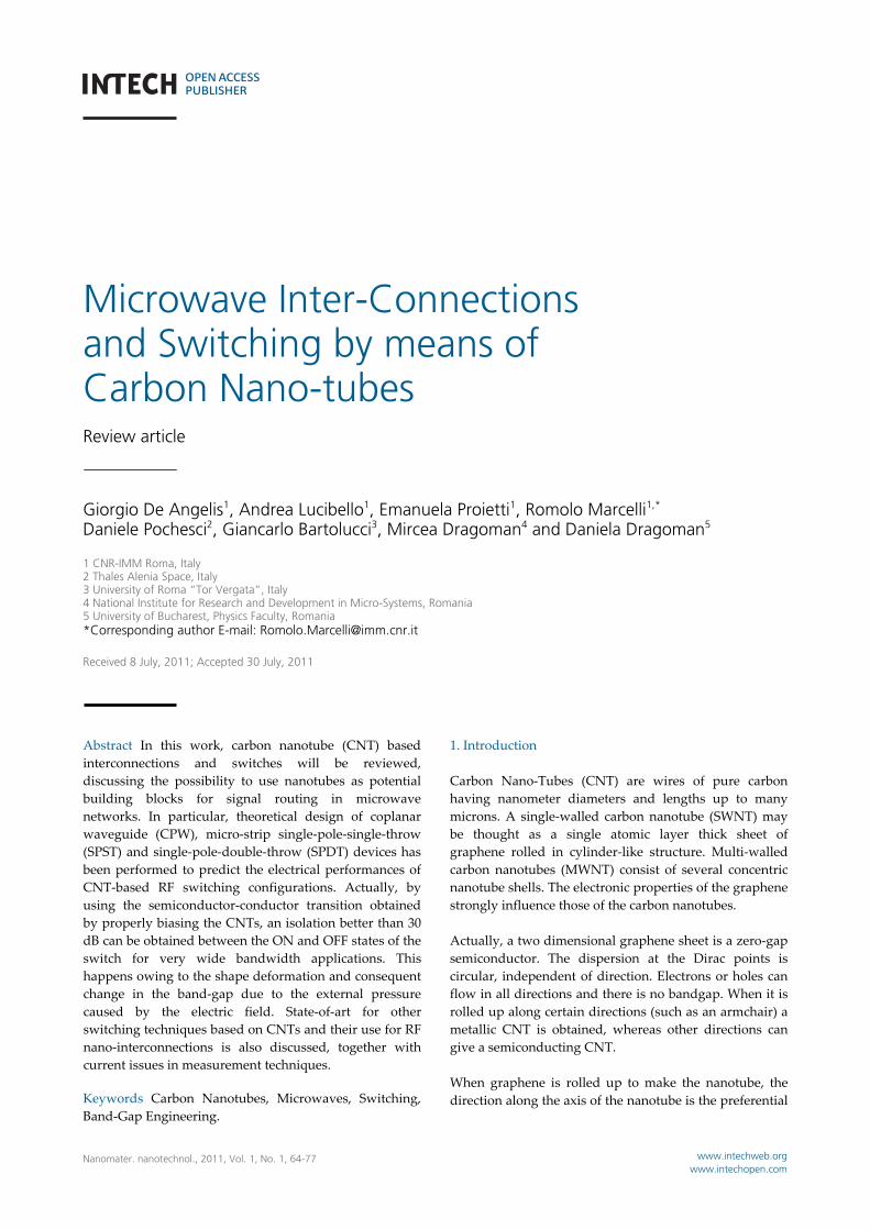
RF and mechanical information about simple transmission line structures or NEMS. Specifically, Agilent is implementing a kind of AFM‐Network, currently based on reflection measurements, to get impedance evaluations on several nano‐configurations, including electronic and biological samples, with some results available specifically for CNT‐FET configurations [27],[28]. Because of the above considerations, the applicability of the high frequency properties of CNT/CNF as individual elements and/or as a bundle are presently a hot topic in RF nano‐electronics. 2.1 Micro‐mechanical Switches based on nano‐electromechanical systems (NEMS) In [24], an interconnect scheme using NEMS varactors is studied, as an extension of MEMS configurations. In that case both the technology for selective growth of CNTs and their driving by using DC bias are described. In particular, PECVD and RIE technologies have been utilized against the more expensive EBL, and preliminary results have been obtained for the actuation voltage (25 volt). Issues have still to be solved about the horizontal positioning of the individual CNTs, but the possibility to use such a solution for tunable small capacitances characterized also by small actuation times renders this technology appealing for nano‐devices. Two configurations of nano‐electromechanical switches have been analyzed and modeled at LAAS‐CNRS [29]. The two concepts are working in the microwave and millimeter wave frequency ranges by using metallic nano‐tubes which are vertically or horizontally positioned with respect to the planar microwave waveguide (CPW) (Fig. 1). This allows to block or enable the electromagnetic field propagation once an electrostatically DC actuation of a few volts is applied between the CPW ground planes and the signal line. Although the dimensions of metallic nanotubes are very small in comparison with the planar waveguide dimensions and the operating wavelengths, these switches are very efficient and agile. The modeled microwave performances show an average insertion loss of 0.5 dB and an average isolation of −23 dB, while the characteristic impedance is 47.2 ohms at 60 GHz. The isolation attains quite high values up to 50 GHz and then decreases down to −16 dB at 100 GHz. These are very good values in an extremely large bandwidth. 2.2 Varactors Varactor based on semiconducting CNT have been demonstrated within a collaboration between IMT Bucarest and LAAS‐CNRS, as schematically drawn in Fig. 2. The
Giorgio De Angelis, Andrea Lucibello, Emanuela Proietti, Romolo Marcelli, Daniele Pochesci, Giancarlo Bartolucci, Mircea Dragoman and Daniela Dragoman: Microwave Inter-Connections and Switching by means of Carbon Nano-tubes
66www.intechweb.orgwww.intechopen.com
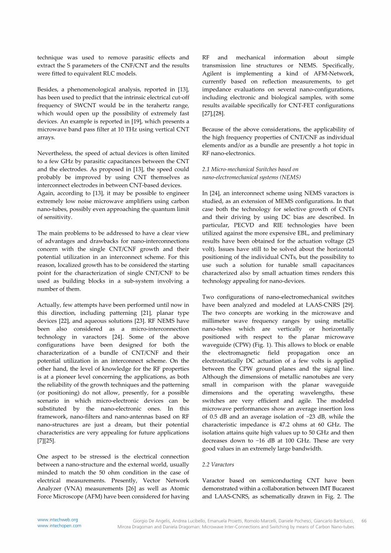
devices show a working range up to a few terahertz under room temperature conditions and a tunability of more than five times when the external applied voltage is tuned up to 6.7 V [30]. Two type of implementations of varactors have been explored, on a single gated nanotube and on a biased array of carbon nanotubes respectively. In the former case, the varactor is made by the density‐of‐states dependent quantum capacitance that can be tuned via a gate voltage due to the shift of the Fermi level. In the latter case, the varactor consists of a selectively biased brushlike carbon nanotube array with a capacitance tuned via attractive and repulsive electrostatic forces between different nanotubes of the array .
(a)
(b)
Figure 1. The two switch configurations with vertically (a) and horizontally (b)aligned metallic CNT. [29]
(a)
(b)
Figure 2. Varactor Schematic representation of the single CNT gate (a) and CNT array configuration (b) [30].
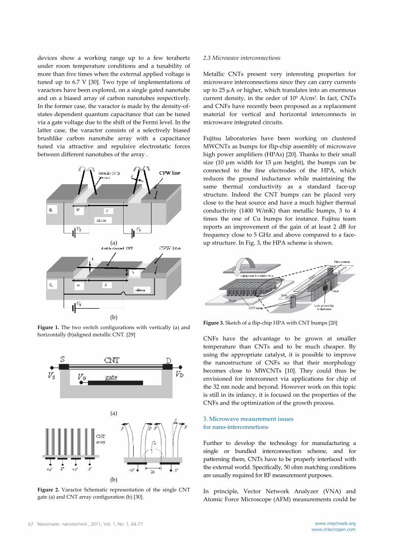
2.3 Microwave interconnections Metallic CNTs present very interesting properties for microwave interconnections since they can carry currents up to 25 A or higher, which translates into an enormous current density, in the order of 109 A/cm2. In fact, CNTs and CNFs have recently been proposed as a replacement material for vertical and horizontal interconnects in microwave integrated circuits. Fujitsu laboratories have been working on clustered MWCNTs as bumps for flip‐chip assembly of microwave high power amplifiers (HPAs) [20]. Thanks to their small size (10 m width for 15 m height), the bumps can be connected to the fine electrodes of the HPA, which reduces the ground inductance while maintaining the same thermal conductivity as a standard face‐up structure. Indeed the CNT bumps can be placed very close to the heat source and have a much higher thermal conductivity (1400 W/mK) than metallic bumps, 3 to 4 times the one of Cu bumps for instance. Fujitsu team reports an improvement of the gain of at least 2 dB for frequency close to 5 GHz and above compared to a face‐up structure. In Fig. 3, the HPA scheme is shown.
Figure 3. Sketch of a flip‐chip HPA with CNT bumps [20] CNFs have the advantage to be grown at smaller temperature than CNTs and to be much cheaper. By using the appropriate catalyst, it is possible to improve the nanostructure of CNFs so that their morphology becomes close to MWCNTs [10]. They could thus be envisioned for interconnect via applications for chip of the 32 nm node and beyond. However work on this topic is still in its infancy, it is focused on the properties of the CNFs and the optimization of the growth process. 3. Microwave measurement issues for nano‐interconnetions Further to develop the technology for manufacturing a single or bundled interconnection scheme, and for patterning them, CNTs have to be properly interfaced with the external world. Specifically, 50 ohm matching conditions are usually required for RF measurement purposes. In principle, Vector Network Analyzer (VNA) and Atomic Force Microscope (AFM) measurements could be
Nanomater. nanotechnol., 2011, Vol. 1, No. 1, 64-7767 www.intechweb.orgwww.intechopen.com

used for characterizing the test structures. Several attempts to perform an overall characterization of the CNTs properties can be found in [48][50]. 3.1 VNA characterizations The classical approach in VNA characterizations is based on de‐embedded measurements taken by means of a calibrated procedure. A CNT/CNF structure can be considered as a wire connecting two I/O ports in coplanar configuration, with the usual ground‐signal‐ground (G‐S‐G) probes bringing the signal to the VNA. In this case, the CNT/CNF is a kind of short microstrip or stripline structure, and the de‐embedding procedure will require a careful characterization of the coplanar–to‐microstrip transition. Particular attention has to be paid for the effects limiting the measurement precision, and specifically to the probe pads. As from recent literature results about a multi‐walled carbon nanotube (MWCNT) [24], the dynamic impedance and the computed Rc and R values significantly decrease with increasing frequency, as also predicted by earlier theoretical work. This clearly shows that MWCNTs are promising as a transmission or interconnect line in the GHz and THz regime. The measurement scheme used in [24] is shown in Fig. 3.
Figure 3. Measurements and modelling (a) schematic diagram of the Cr/Au bi‐layer electrodes fabricated for ground–signal–ground probing, (b) equivalent circuit model for a sample with an MWCNT. The dotted circle represents the MWCNT part. Cp and Rp denote the capacitance and resistance of the probing pads, Cps denote the parasitic capacitance of the gap, Rc and Cc denote the contact resistance and capacitance between the MWCNT and the electrodes, and R, L, C are the resistance, inductance, capacitance of the MWCNT. [24] The more delicate technological problem in this measurement approach is given by the contact pads, which in order to improve the contact with the MWCNT were designed to be a gradually narrowed shape from the RF Probes to the MWCNT. As described in [24], the electrodes were made of Cr/Au (5/150 nm) bi‐layer at a low deposition rate (0.01 nm s–1), to accommodate the full wrapping of the MWCNT by Au. In Fig. 4 (b) is shown
the connection of the IN/OUT electrodes by an MWCNT. In this case, the gap between the electrodes is 4 μm, and the MWCNT extends into the electrode about 2 μm on either side. For comparison and de‐embedding of the parasitic effects from the measured data, the identical pad structures without an MWCNT (OPEN), and with an Au wire of 2 μm in diameter (SHORT), were also fabricated.
Figure 4. Photos from Fig. 1 of [26]. A sample prepared for two‐port S‐parameter measurements (a) TEM image of a selected CNT, (b) SEM image of the CNT part of the sample, which shows an MWNT connecting the IN/OUT electrodes. In that paper is commented the recorded difference with respect to the SWCNT data [33], where no significant frequency dependence of the impedance has been evidenced. This is an item to be stressed in the next future, especially for the utilization of CNT in low frequency interconnections. In [33] the small imaginary part of the S‐parameters, as compared to the real part, is taken as a sign that the nano‐tube impedance is mostly real and does not depend on the frequency. The measured magnitude ratios in literature between the real and imaginary parts of these two experiments seem similar (10:1 versus 9:1) in the lower frequency region. However, the magnitude of S11 phase data increases with the frequency. Also, S11 data of samples with and without MWCNT are very similar, but the S21 data are distinct. In conclusion, in the two‐port measurements, it seems that the S11 data are affected more by the pads or parasitic effects, rather than by the MWCNT, whereas the S21 data contain rich information. So far, particular attention has to be paid in the de‐embedding technique and in the identification of the standards to be used for a proper calibration. TRL methods should be designed and then compared to the method used in the above presented approach, and, possibly, different lengths of the CNT to check the results obtained by Burke in 2004, about the experimental verification of the dynamical impedance of a metallic SWCNT, which should be dominantly real and frequency independent from DC to 10 GHz, with the resistance lower than a similar sized copper wire. Different lengths of the CNT/CNF structures would be also useful in typical TRL calibration techniques for setting the frequency range for the measurements. Actually, TRL de‐embedding procedures are usually minded for general high frequency characterizations, and they are particularly useful for on‐wafer measurements,
Giorgio De Angelis, Andrea Lucibello, Emanuela Proietti, Romolo Marcelli, Daniele Pochesci, Giancarlo Bartolucci, Mircea Dragoman and Daniela Dragoman: Microwave Inter-Connections and Switching by means of Carbon Nano-tubes
68www.intechweb.orgwww.intechopen.com

where it is easier to provide multi‐length standards than specific components like a broad‐band load. Moreover, the analytical approach is simplified in the TRL with respect to the SHORT‐OPEN‐LOAD‐THROW (SOLT) calibration. So far, TRL is not specifically oriented on CNTs, but is intended for broader range of potential nanoscale devices with impedances significantly different from the 50 Ohm impedance of the measurement systems. On the other hand, it needs several improvements because of the quantistic approach to be used in describing the propagation of a high frequency signal, as already discussed by Burke [9]. In commercially available VNA equipments, physical modeling is often approximated by simple polynomial expressions. In this case, we guess that arbitrary functions properly accounting for the physics of the problem, and post‐processing of data are both fundamental steps for obtaining not only a good characterization, but also a deeper knowledge of the involved physical mechanisms. Mostly, in literature high frequency performances of CNTs are focused on FET structures, like in [34], because of the very promising applications in this kind of devices. For such a structure, impedance modeling following previous theoretical results have been also proposed in [35][36]. Other interesting results concern with the dielectric characterization of CNT‐based composites and related calibration of the measurement system [37]. A very interesting and original approach for high frequencies has been recently developed by using a Wheatstone bridge, and performing a differential analysis of the CNT inserted in the network as a fourth resistor [38]. In this way, impedance measurements were possible. Time domain characterization, to be implemented also for RF nano‐structures, has been proposed in [39]. Rarely the problem is treated for passive structures only. An extension on transmission line modeling based on past results, inspired by the Boltzmann Transport Equation is given in [40][41] and related references. Besides the above considered configurations and the FET ones available in literature, minded for testing CNTs as nano‐electronic components to be used even onto flexible substrates [42], an alternative approach of a configuration for testing individual CNT/CNF can be found in [24], where suspended CNTs are considered for varactor applications. It offers the possibility to re‐model such a structure, originally minded for switching applications, to test individual CNTs. In this case, the same VNA calibration and characterization techniques could be used. In summary, several results are currently available on CNT characterization for RF applications, but few of them are really minded for nano‐interconnections. In particular, commercial network analysis instruments need to be updated for both, external interconnection capabilities and calibration software, to provide a standard and reliable system for measuring CNTs.
3.2 AFM characterizations Because of the previously outlined difficulties in measuring the RF properties of CNTs, an alternative technique has been recently introduced based on the atomic force microscope (AFM) technique. Actually, nano‐scale devices exhibit typically very high impedance; while Network Analyzers are optimized, as discussed before, at 50 ohms. Probing solutions for the nano‐scale do not exist and the Atomic Force Microscopes can provide a platform for approaching this issue. In this case we need new application specific calibration standards and an Arbitrary Impedance Network Analyzer. In such a way the Scanning Microwave AFM will begin to provide nano‐scale solutions, as currently studied by the the Delft University in collaboration with the Agilent Company and by the National Institute for Standard and Technology (NIST) in USA. Scanning microwave microscopy (SMM) measurements are currently reflection only, and a repetitive “tip up” (open circuit) calibration before every “tip down” measurement is needed. In this SMM approach, the capacitance is the main physical property that can be measured [43]. NIST is currently studying how to improve some of the calibration standards, like the substrate. In the case of semiconductors one of the main quantity to be controlled is the doping concentration as a function of the depth without destroying the wafer. Bias to the tip while measuring S11 is provided. This allows to perform “dC/dV” measurements as a function of depletion depth for microelectronic devices diagnostics . In general, the usual SHORT‐OPEN‐LOAD‐THROW (SOLT) calibration standards are not applicable to this world, and they should be application specific.
Figure 5. The VNA approach for RF reflection measurements. [45]. It is worth noting that Near Field Microscopy can also be extended to THz frequencies, as in the characterization of the Goubau line, which consists of a single conductor coated with dielectric material, as given in [44]. A
Nanomater. nanotechnol., 2011, Vol. 1, No. 1, 64-7769 www.intechweb.orgwww.intechopen.com
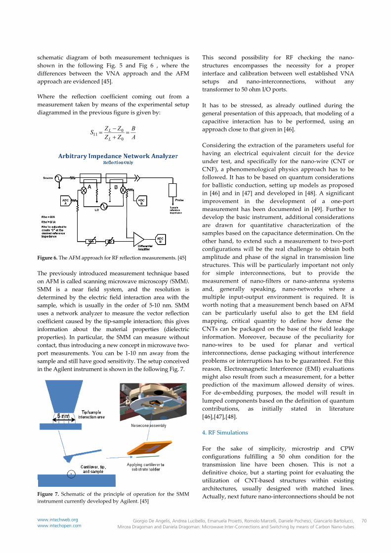
schematic diagram of both measurement techniques is shown in the following Fig. 5 and Fig 6 , where the differences between the VNA approach and the AFM approach are evidenced [45]. Where the reflection coefficient coming out from a measurement taken by means of the experimental setup diagrammed in the previous figure is given by:
AB
ZZZZS
L
L
0
011
Figure 6. The AFM approach for RF reflection measurements. [45] The previously introduced measurement technique based on AFM is called scanning microwave microscopy (SMM). SMM is a near field system, and the resolution is determined by the electric field interaction area with the sample, which is usually in the order of 5‐10 nm. SMM uses a network analyzer to measure the vector reflection coefficient caused by the tip‐sample interaction; this gives information about the material properties (dielectric properties). In particular, the SMM can measure without contact, thus introducing a new concept in microwave two‐port measurements. You can be 1‐10 nm away from the sample and still have good sensitivity. The setup conceived in the Agilent instrument is shown in the following Fig. 7.
Figure 7. Schematic of the principle of operation for the SMM instrument currently developed by Agilent. [45]
This second possibility for RF checking the nano‐structures encompasses the necessity for a proper interface and calibration between well established VNA setups and nano‐interconnections, without any transformer to 50 ohm I/O ports. It has to be stressed, as already outlined during the general presentation of this approach, that modeling of a capacitive interaction has to be performed, using an approach close to that given in [46]. Considering the extraction of the parameters useful for having an electrical equivalent circuit for the device under test, and specifically for the nano‐wire (CNT or CNF), a phenomenological physics approach has to be followed. It has to be based on quantum considerations for ballistic conduction, setting up models as proposed in [46] and in [47] and developed in [48]. A significant improvement in the development of a one‐port measurement has been documented in [49]. Further to develop the basic instrument, additional considerations are drawn for quantitative characterization of the samples based on the capacitance determination. On the other hand, to extend such a measurement to two‐port configurations will be the real challenge to obtain both amplitude and phase of the signal in transmission line structures. This will be particularly important not only for simple interconnections, but to provide the measurement of nano‐filters or nano‐antenna systems and, generally speaking, nano‐networks where a multiple input‐output environment is required. It is worth noting that a measurement bench based on AFM can be particularly useful also to get the EM field mapping, critical quantity to define how dense the CNTs can be packaged on the base of the field leakage information. Moreover, because of the peculiarity for nano‐wires to be used for planar and vertical interconnections, dense packaging without interference problems or interruptions has to be guaranteed. For this reason, Electromagnetic Interference (EMI) evaluations might also result from such a measurement, for a better prediction of the maximum allowed density of wires. For de‐embedding purposes, the model will result in lumped components based on the definition of quantum contributions, as initially stated in literature [46],[47],[48]. 4. RF Simulations For the sake of simplicity, microstrip and CPW configurations fulfilling a 50 ohm condition for the transmission line have been chosen. This is not a definitive choice, but a starting point for evaluating the utilization of CNT‐based structures within existing architectures, usually designed with matched lines. Actually, next future nano‐interconnections should be not
Giorgio De Angelis, Andrea Lucibello, Emanuela Proietti, Romolo Marcelli, Daniele Pochesci, Giancarlo Bartolucci, Mircea Dragoman and Daniela Dragoman: Microwave Inter-Connections and Switching by means of Carbon Nano-tubes
70www.intechweb.orgwww.intechopen.com

limited to such a constraint, because in down‐sizing the device we shall be forced to renormalize the required electrical matching at the nano level [7]. For all of the following simulations we have assumed a six orders of magnitude change in the conductivity induced by the metal‐semiconductor transition [1]. This is also an assumption dependent on the growth technique used for obtaining the CNT structures [51][52][53][54][55][57], still in progress depending on the required application. 4.1 Microstrip configurations First of all, a micro‐strip configuration with a 50 ohm matched line and an in‐line capacitive gap of 50 μm has been simulated by using the HFSS 3D Electromagnetic Software Package. The exploited device is shown in Fig. 8, while in Fig. 9 the expected performances are plotted.
Figure 8. Simulation of a 50 Ohm switch in micro‐strip configuration, with a bundle of CNTs filling a gap. The ON and OFF states depend on the metal‐semiconductor transition.
0 1 0 2 0 3 0 4 0- 6 0
- 5 0
- 4 0
- 3 0
- 2 0
- 1 0
0
S 1 1 O N S 2 1 O N S 1 1 O F F S 2 1 O F F
S-P
aram
eter
[dB
]
F r e q u e n c y [G H z ]
Figure 9. Simulation results for the scattering parameters for the ON and OFF states of the CNT‐based switch. The matching is very good for the ON state until 40 GHz After that, a SPDT based on the same micro‐strip has been simulated, as it is shown in Fig. 10, where a matched micro‐strip SPDT is diagrammed, with two gaps filled with CNTs, to be used with or without a biasing to drive the metal‐semiconductor transition. In Fig. 11 the results in terms of S‐parameters are shown, with evidence for negligible losses on the arm where the CNT is metallic (ON state) and quite good isolation on the arm where the CNT is in the OFF state (15 dB)
up to 10 GHz. In this case a gap of 50 μm has been designed, but an increase in the electrical performances is expected when wider gaps are considered.
Figure 10. Simulated SPDT structure. A 50 ohm matched SPDT device has been obtained by using Au metallization on a high resistivity, oxidized, Silicon wafer. The Au lines are 523 μm wide and 2 μm thick, while 50 μm gaps have been filled with CNT in ON/OFF states.
0 2 4 6 8 10-50
-40
-30
-20
-10
0
S11 S21 S31
S-P
aram
eter
[dB
]
Frequency [GHz]
Figure 11. Simulation results for the scattering parameters of the SPDT microstrip structure. In this case, on port 3 has been imposed the condition for the CNT ON state, thus allowing the transmission of the signal with port 2 isolated (CNT in OFF state). As an alternative with respect to the previous micro‐strip configuration, a dual‐layer structure has been also considered, with a via‐hole filled by a bundle of CNTs connecting two micro‐strip lines used as I/O transmission lines. The device, electromagnetically simulated by using the Microwave Office AWR Software is shown in Fig. 12, while in Fig. 13 the performances for the ON/OFF states of the switch are plotted. In this case, the OFF state for the switch means the ON state for the CNT (metallic) and viceversa.
Port 1
Port 2
Port 3
CNT OFF/ON
CNT ON/OFF
Port 1
Port 2
CNTON/OFF
Nanomater. nanotechnol., 2011, Vol. 1, No. 1, 64-7771 www.intechweb.orgwww.intechopen.com

Figure 12. Simulation of a 50 Ohm switch in a micro‐strip dual‐layer configuration with a via hole filled by a bundle of CNTs. Dimensions are in micron.
0 10 20 30 40-25
-20
-15
-10
-5
0
5
14 dB10 dB
18 dB
ON State
OFF State
Tran
smis
sion
[dB
]
Frequency [GHz]
Figure 13. Simulation results for the scattering parameters for the microstrip dual‐layer configuration using a bundle of CNTs. The transmission signal decreases rapidly with the frequency. 4.2 Coplanar Waveguide Configurations Two possible technological approaches have been considered also for the SPST devices in coplanar configuration. First of all, a 50 ohm CPW line has been simulated by using an array of CNT directed orthogonally with respect to the central conductor of the CPW, and in the same plane. In this case the CNT are defined in a patch having dimensions 100x50 μm2. The device is shown in Fig. 14 and the response in transmission is given in Fig. 15.
Figure 14. CPW switch with CNTs (green in the figures) aligned orthogonally with respect to the central conductor, in the plane of the substrate.
0 10 20 30 40-45-40-35-30-25-20-15-10-505
>= 15 dB
> 20 dBON State
OFF State
Tran
smis
sion
[dB
]
Frequency [GHz]
Figure 15. Simulated response of the CPW switch with horizontally placed CNTs. After that, a via‐hole filled by CNTs vertically aligned with respect to the substrate, has been introduced along the CPW, having the same planar dimensions of the previously defined patch, but going inside a dielectric structure with a total thickness of 20 μm. The configuration used for the simulation and the expected results are given in Fig. 16 and in Fig. 17 respectively. From the comparison of all of the above configurations, the most promising one looks to be the CPW based device presented in Fig. 16 having the electrical performances predicted in Fig. 17, where a wideband high ratio between the ON and OFF states is expected.
Giorgio De Angelis, Andrea Lucibello, Emanuela Proietti, Romolo Marcelli, Daniele Pochesci, Giancarlo Bartolucci, Mircea Dragoman and Daniela Dragoman: Microwave Inter-Connections and Switching by means of Carbon Nano-tubes
72www.intechweb.orgwww.intechopen.com

21 2
Figure 16. Top view of the simulated structure. The green boxes are via‐holes filled by vertically grown CNTs. The shaded narrow area under the plane of the CPW, orthogonal with respect to the central conductor, is a Au strip providing a ground reference in common for the RF and for the DC signals.
0 10 20 30 40-45-40-35-30-25-20-15-10
-505
30 dB35 dB
ON State
OFF StateTran
smis
sion
[dB
]
Frequency [GHz]
Figure 17. Electrical response in transmission of the CNT based CPW switch. 5. Band‐gap engineering of carbon nano‐tubes. Pressure dependence of the shape and conductivity The possibility to use electromagnetic or transport properties instead of movable parts for switching, like in the case of MEMS, should involve an increased reliability of the device, no more subjected to electro‐mechanical or charging failures. On the other hand, FET configurations are already available for doing the same job, but drawbacks of FETs based on semiconductor hetero‐structures are both the intrinsic non‐linearity of the device, which influences the signal purity, and the insertion losses. Other materials like Vanadium Oxide have been already used in the past for optical applications, opening the way for switching mechanisms based on changes of the refractive index n [58][59]. Liquid
Crystals (LC) have been also recently proposed for providing a fine tuning in the microwave range, by means of the change in the dielectric constant.
Figure 18. Shape deformation of the cross‐section of a CNT due to external pressure [63]. The findings in the previous section are based on the assumption that it is possible to perform a kind of band‐gap engineering on the CNTs by means of pressure. This is due to the conductor‐semiconductor transition driven by the cross section deformation of the nano‐tube. In fact, further to have functionalized CNTs, which can change their electronic and optical properties by means of doping [60], the mechanical pressure exerted on metallic CNTs squashes them [61], while a hydrostatic pressure [62] induces radial deformations on CNTs, as indicated in Fig. 18. The shape deformation from circle to ellipse is dominated by the competition between compression, which reduces the perimeter, and bending, which increases the curvature of the CNT. Beyond a certain pressure P1 the bending process is dominant, this threshold pressure between the circular and the ellipse shape being given by:
31 24dRP F (1)
Where RF is the flexural rigidity. The other threshold pressures for shape deformations are:
1
313
1
212
ln
ln
AABPP
AABPP
(2)
where A1 A2 , and A3 are the cross‐section areas of the CNT at pressures P1 , P2 , and P3 , respectively, and B is the radial modulus of the tube after the first shape transition. Because the ratio A2 / A1 ≈ 0.81 is independent of the tube radius, we obtain P2 ≈ 1.2P1. At the pressure P3 the metallic CNT experiences a transition towards a semiconductor CNT, the metal‐semiconductor transition being identified by measuring the conductance dependence on the dc voltage applied to the CNT. At the metal‐insulator transition a gap opens, manifested by the decrease of the CNT conductance with two orders of
Nanomater. nanotechnol., 2011, Vol. 1, No. 1, 64-7773 www.intechweb.orgwww.intechopen.com

magnitude. This gap is about 0.2 eV for a (10,10) metallic CNT. The pressure P3 decreases if the diameter of the CNT increases. For example, P3 is 8.5 GPa for a (6,6) metallic nanotube, it becomes 2 GPa for a (10,10) metallic nanotube, while for a (100,100) metallic nano‐tube P3 is only 3 kPa. The pressures P1 and P2 show the same behaviour. The axial strain applied on a semiconducting CNT increases or decreases the band‐gap, depending on the type of the strain [63]. The gap variation as a function of the strain s is given in this case by [64]
3cos1312sgn 0 pdsdEg (3)
where v is the Poisson ratio, n and m satisfy the condition n ‐ m =3i + p , with p = –1, 0, or 1 and i is an integer number. The semiconductor CNTs with p =1 have dEg / ds >0 , while those with p =‐1 have dEg / ds <0 . The controllable increase or decrease of the band gap of semiconductor CNTs under strain can be used to band‐gap engineering of hetero‐structures, as in the case of III‐V semiconductors. The axial strain applied on a metallic CNT via an AFM cantilever generates a metallic‐semiconductor transition, during which the conductance decreases with orders of magnitude, as in the case of CNT squashing. The conductance depends on strain as
12
0 exp18
TkE
heG
B
g (4)
The electronic properties of individual semiconducting CNTs can be controlled by chemical doping, which tunes the Fermi energy level value in either the conduction band (for an n‐type CNT) or in the valence band (for a p‐type CNT). At room temperature and in a normal atmospheric pressure the semiconductor CNT is not intrinsic (n=p), but is of p‐type, so that the electronic properties are dictated by holes, whose concentration is dominant. The natural p‐type doping of semiconductor CNTs was first explained as a chemical contamination and was attributed either to the charge transfer from metal contacts, which are patterned over the CNT, or to adsorbed molecules, such as oxygen or chemical groups, with which the CNT is in contact when patterned on various types of substrates. Nevertheless, it was demonstrated that neither adsorbed molecules nor chemical groups induces the p‐type behavior. Rather, the
origin of the p‐type behavior is the self‐doping phenomenon [65], which is specific to nano‐scale materials and is caused by the curvature of the CNT. More precisely, the intrinsic dominant hole concentration is due to a curvature‐induced charge redistribution among the bonding orbitals, this re‐hybridization of atom orbitals depending strongly on the tube diameter. The rapid decrease of the number of holes per C atom when the CNT diameter increases is supported by various experiments. The p‐type intrinsic concentration, which resides in the geometry of the CNT, increases the strength of π bond and induces a π‐σ charge transfer, manifested by electron depletion from the π valence band. As a consequence of the above discussion, we can now go back to the geometry proposed in Fig. 16 to evaluate the bias voltage necessary for providing enough pressure to cause the conductor‐semiconductor transition. As well established, the electrostatic force Fe generated by a parallel plate capacitor can be written as :
2
21 V
zCF
gze
(5)
Where C(z) is the capacitance as a function of the separation of the two electrodes, to be computed at the distance g between them, and V is the applied voltage. By assuming the presence of air between the two electrodes, and being A the area of each of them:
Agz
CgAgC
gz200 ;)(
(6)
In particular, the nano‐tubes have been considered in a volume having planar dimensions 100x50 μm2 (100 along the CPW central conductor and 50 orthogonal with respect to it) and 20 μm depth, we can say that A=50x20x10‐12 m2=10‐10 m2, whereas g=10‐4 m. Since ε0=8.85x10‐12 in SI units, it will be: Fe=‐0.5x(8.85x10‐12x10‐10/10‐8) V2=4.4x10‐14 V2 N, from which the pressure results to be: P=4.4x10‐4 V2 Pa. For practical applications, no more than 50 volt should be reasonably applied for switching purposes, which means to obtain a pressure P in the order of 1 Pa, well below the threshold needed for the transition predicted for different configurations of CPW based switches. On the other hand, as stressed at the beginning, the utilization of nano‐tubes imposes the passage to a new kind of logic, where interconnections and switching should be possible at the nano‐level. In this
Giorgio De Angelis, Andrea Lucibello, Emanuela Proietti, Romolo Marcelli, Daniele Pochesci, Giancarlo Bartolucci, Mircea Dragoman and Daniela Dragoman: Microwave Inter-Connections and Switching by means of Carbon Nano-tubes
74www.intechweb.orgwww.intechopen.com
framework, a tapering of the line could reduce by a factor 10 the linear size of the region where the CNT is present, and by using the same voltage a quadratic effect is obtained on the separation term, thus obtaining more realistic values for the threshold pressures. Moreover, CNTs could be embedded in a dielectric, as it is the case of nano‐interconnection modules, and the capacitance value can be consequently augmented, favouring an enhancement of the electrical force. 6. Conclusion CNT‐based interconnections and switches have been reviewed, with emphasis for the possibility to use nano‐tubes as building blocks in microwave signal processing. In particular, microstrip and coplanar waveguide configurations have been studied exploring the potentialities not only for nano‐interconnections and switches based on electromechanical solutions, but also with band‐gap engineering using an external pressure to drive the semiconductor‐conductor transition. As a result, properly biased bundles of CNTs can be forced by means of an external DC electric field which reshapes the nano‐tube, modifying the band‐gap and causing a transition from the semiconductor to the conductor state. Simple, electrically matched configurations have been simulated, and the coplanar structure with nano‐tubes vertically aligned and properly grounded has been found to be the best solution for providing a high ON/OFF ratio due to the transition. Further improvements are necessary in order to tailor the area where CNTs have to be grown, to lower the voltage necessary for driving the semiconductor‐conductor transition. 7. References [1] M. Dragoman et al, “Reversible metal‐semiconductor
transitions for microwave switching applications”, Appl. Phys. Lett. 88, 073503 (2006)
[2] M. Dragoman et al., “Experimental determination of microwave attenuation and electrical permittivity of double‐walled carbon nanotubes”Appl. Phys. Lett. 88, 153108 (2006)
[3] M. S. Marcus et al., « Photogating carbon nanotube transistors”, J. Appl. Phys 100, 084306 (2006)
[4] http://www.physics.umd.edu/mfuhrer/ntresearch.htm#Conductance
[5] G. M. Rebeiz, “RF MEMS, Theory, Design and Technology”, John Wiley and Sons, Hoboken, 2003.
[6] Giancarlo Bartolucci, Romolo Marcelli, Simone Catoni, Benno Margesin, Flavio Giacomozzi, Viviana Mulloni, Paola Farinelli: “An Equivalent Circuital Model for Shunt Connected Coplanar RF MEMS Switches”; Journal of Applied Physics, Vol. 104, No. 8, pp.84514‐1 ‐ 84514‐8 (2008).
[7] Pierantoni, L. Coccetti, F. Russer, P., « Nanoelectronics: The Paradigm Shift », IEEE Microwave Magazine, Vol.11, issue, Dec.2010
[8] Andrea G. Chiariello et al., “Metallic Carbon Nanotube Interconnects, Part II: a Transmission Line Model”, Proceed. of IEEE – ISP2006, 185 (2006)
[9] Burke P. J., “An RF Circuit Model for Carbon Nanotubes”, IEEE Trans. on Nanotechn,. Vol. 2 No. l, 55 (2003)
[10] Quoc Ngo, T. Yamada, M. Suzuki, Y. Ominami, A.M. Cassell, Li Jun, M. Meyyappan and C. Y. Yang. “Structural and Electrical Characterization of Carbon Nanofibers for Interconnect Via Applications” IEEE Transactions on Nanotechnology, Volume 6, Issue 6, Nov. 2007, pp. 688 – 695.
[11] F. Kreupl, A.P. Graham, G.S. Duesberg, W. Steinhögl, M. Liebau, E. Unger and W. Hönlein “Carbon nanotubes in interconnect applications” Microelectron. Eng. 64, 1 (Oct. 2002), pp. 399‐408.
[12] J. C. Coiffic, L. E. Foa Torres, H. Le Poche, M. Fayolle, S. Roche, S. Maitrejean, S. Roualdes, A. Ayral “An application of carbon anotubes for integrated circuit interconnects”, Proceed. SPIE, Vol. 7037, paper 7037 D‐1 (2008).
[13] P. Burke, “AC performance of nanoelectronics: toward a ballistic THz nanotube transistor”; Solid‐State Electronics 48 (2004).
[14] Francisco R. Madriz, John R. Jameson, Shoba Krishnan, Kris Gleason, Xuhui Sun and Cary Y. Yang. “Measurements and Circuit Model of Carbon Nanofibers at Microwave Frequencies”. Interconnect Technology Conference 2008, 1‐4 June 2008, pp. 138 – 140.
[15] P.J. Burke, Z. Yu, S. Li, and C. Rutherglen. “Nanotube Technology for Microwave Applications”, Digest, 2005 IEEE MTT‐S.
[16] N.N. Al Moayed, U.A. Khan, M. Obol, S. Gupta and M.N. Afsar. “Characterization of Single‐ and Multi‐walled Carbon Nanotubes at Microwave Frequencies”. Proceedings of the Instrumentation and Measurement Technology Conference, IEEE 2007, 1‐3 May 2007, pp.1 – 4.
[17] J.J. Plombon et al., “High‐frequency electrical properties of individual and bundled carbon nanotubes”, Applied Physics Letters, Vol. 90, Issue 6, 2007.
[18] Min Zhang, Xiao Huo, P.C.H. Chan, Qi Liang and Z.K. Tang. “Radio‐frequency transmission properties of carbon nanotubes in a field‐effect transistor configuration”, Electron Device Letters, Volume 27, Issue 8, Aug. 2006, pp. 668 – 670.
[19] M. Al Ahmad, A. Tahraoui, W. I. Milne and R. Plana. “Metallic multiwalled carbon nanotubes for microwave applications”, Semiconductor Device Research Symposium, IEEE 2007, 12‐14 Dec. 2007.
Nanomater. nanotechnol., 2011, Vol. 1, No. 1, 64-7775 www.intechweb.orgwww.intechopen.com

[20] Taisuke Iwai, Yuji Awano, “Carbon Nanotube bumps for thermal and electric conduction in transistor”, Fujitsu Sci. Tech. J., 43, 4, p.508‐515, October 2007.
[21] J. Chae, X. Ho, J. A. Rogers, K. Jain, “Patterning of single‐walled carbon nanotubes using a low‐influence excimer laser photoablation process”, Proceed. SPIE, Vol. 7037, paper 7037 0‐M (2008).
[22] D. Pribat, M. Gowtham, C. Cojocaru, B. Marquardt, A. Q. L. Quang, “Novel approach to align carbon nanotubes for planar type devices”, Proceed. SPIE, Vol. 7037, paper 7037 0‐N (2008).
[23] S. Shoji, T. Roders, “Light induced accumulation of single‐wall carbon nanotubes dispersed in aqueous solution”, Proceed. SPIE, Vol. 7037, paper 7037 0‐O (2008).
[24] S. Pacchini, M. Dilhan, T. Ricart, C. Cojocaru, D. Pribat, D. Dubuc and K. Grenier: “ Micro‐Interconnection technology suitable for RF‐NEMS varactors elaboration, Proceed. SPIE, Vol. 7037, paper 7037 19 (2008).
[25] M. Dragoman and D. Dragoman, “Nanoelectronics Principles and Devices”, Artech House 2006.
[26] Seong Chan Jun, X M H Huang, Sungwon Moon, H Jin Kim, James Hone, Y W Jin and J M Kim, “Passive electrical properties of multi‐walled carbon nanotubes up to 0.1 THz”, New Journal of Physics 9 (2007) 265 (2007)
[27] Measuring CNT FET’s and SET’s Using the B1500A, Agilent Application Note B1500‐1, http://nano.tm.agilent.com/index.cgi?CONTENT_ID=406&User:LANGUAGE=en‐US
[28] Using the Agilent B1500A with a Nanoprober to Perform Failure Analysis, Agilent Application Note B1500‐7, http://nano.tm.agilent.com/index.cgi?CONTENT_ID=406&User:LANGUAGE=en‐US
[29] M.Dragoman et al. , “Nanoelectromechanical switches based on carbon nanotubes for microwave and millimeter waves”, Journal of Applied Physics, 90, 113102, 2007.
[30] M. Dragoman et al, “Variable capacitance mechanisms in carbon nanotubes” Journal of Applied Physics, 101, 036111, 2007.
[31] K.B.K. Teo et al., “Carbon nanotube technology for solid state and vacuum electronics”, IEE Proc.‐Circuits Devices Syst., Vol. 151, No. 5, October 2004
[32] Shengdong Li, Zhen Yu, Sheng‐Feng Yen, Peter J. Burke, W.C. Tang, “Carbon Nanotube GHz Nano‐Resonator”, Proc. MTT‐S 2004
[33] Z. Yu and P. J. Burke, “Microwave Transport in Metallic Single‐Walled Carbon Nanotubes”, Nano Lett., 2005, 5 (7), pp 1403–1406.
[34] Jing Guo, Sayed Hasan, Ali Javey, Gijs Bosman, and Mark Lundstrom, “Assessment of High‐Frequency Performance Potential of Carbon Nanotube
Transistors”, IEEE Trans. on Nanotechnology, VOL. 4, NO. 6, Nov. 2005, pp.715‐721.
[35] Y. Xu and A. Srivastava, “A Two Port Network Model of CNT‐FET for RF Characterization”, IEEE 50th Midwest Symposium on Circuits and Systems, 2007.
[36] Myung‐Gil Kangm, et al. “Microwave Characterization of a Field Effect Transistor with Dielectrophoretically‐Aligned Single Silicon Nanowire”, Japanese Journal of Applied Physics 49 (2010) 06GG12.
[37] Emmanuel Decrossas and Samir M. El‐Ghazaly,”Microwave Dielectric Characterization of Carbon Nanotube Networks”, Chapter 9 in InTech Publisher Book Carbon Nanotubes ‐ From Research to Applications, pp.146‐156 (2010).
[38] L. Nougaret, G. Dambrine, S. Lepilliet, H. Happy, N. Chimot, V. Derycke, and J.‐P. Bourgoin, Gigahertz characterization of a single carbon nano tube, Appl. Phys. Lett. 96, 042109 (2010)
[39] Fred Chen, Anantha Chandrakasan, Vladimir Stojanovic, “An Oscilloscope Array for High‐Impedance Device Characterization”, ESSCIRC, 2009. ESSCIRC ʹ09. Proceedings of. 2009. 112‐115.
[40] Mahmoud A. EL Sabbagh and Samir M. El‐Ghazaly, “Frequency‐Dependent Circuit Models of Carbon Nanotube Networks”, IEEE 18th Conference on Electrical Performance of Electronic Packaging and Systems, 2009. EPEPS ʹ09.
[41] Fang Zhou,” Transmission line model of carbon nanotubes: through the Boltzmann transport equation”, Journal of Semiconductors, Vol. 32, No. 6, pp. 062002‐1 ‐ 062002‐5 (2011).
[42] M. F. Goffman, N. Chimot, E. Mile, M. C. Monteverde, J.‐P. Bourgoin, V. Derycke, “High frequency carbon nanotube devices”, Proceed. SPIE, Vol. 7037, paper 7037 02 (2008).
[43] Hassan Tanbakuchia, Matt Richtera, Ferry Kienbergera, Hans‐Peter Huber, “Nanoscale Materials and Device Characterization via a Scanning Microwave Microscope”, IEEE International Conference on Microwaves, Communications, Antennas and Electronics Systems, 2009. COMCAS 2009.
[44] M. B. Byrne, J. Cunningham, K. Tych, A. D. Burnett, M. R. Stringer, C. D. Wood, L. Dazhang, M. Lachab, E. H. Linfield, and A. G. Davies, “Terahertz vibrational absorption spectroscopy using microstrip‐linewaveguides”, Appl. Phys. Lett. 93, 182904 (2008)
[45] Roger Stancliff, “Near‐Field Microwave to THz microscopy: instruments, applications, and calibration challenges”, http://resource.npl.co.uk/docs/networks/electromagnetics/mmwug/081111/stancliff.pdf, Agilent Presentation at La Sapienza University ‐ Rome, Nov 13, 2008.
Giorgio De Angelis, Andrea Lucibello, Emanuela Proietti, Romolo Marcelli, Daniele Pochesci, Giancarlo Bartolucci, Mircea Dragoman and Daniela Dragoman: Microwave Inter-Connections and Switching by means of Carbon Nano-tubes
76www.intechweb.orgwww.intechopen.com
[46] P. J. Burke, I. B. Spielman, J. P. Eisenstein, L. N. Pfeiffer, and K. W. West, ʺHigh frequency conductivity of the high‐mobility two‐dimensional electron gas”, Applied Physics Letters, vol. 76, pp. 745‐747, 2000.
[47] Yang Chai, Min Zhang, Jingfeng Gong and Philip C. H. Chan, “Reliability Evaluation of Carbon Nanotube Interconnect in a Silicon CMOS Environment”, Proceed. of International Conference on Electronic Materials and Packaging, 2006. EMAP 2006.
[48] P. Russer and U. Siart Editors, “The Combined Schrödinger‐Maxwell Problem in the Electronic/Electromagnetic Characterization of Nanodevices”, Springer Proceedings in Physics 121, Springer Berlin Heidelberg (2008)
[49] Huber, H. P. Moertelmaier, M. Wallis, T. M. Chiang, C. J. Hochleitner, M. Imtiaz, A. Oh, Y. J. Schilcher, K. Dieudonne, M. Smoliner, J. Hinterdorfer, P. Rosner, S. J. Tanbakuchi, H. Kabos, P. Kienberger, F., “Calibrated nanoscale capacitance measurements using a scanning microwave microscope”, Rev. Scient. Instr., 81, 113701 (2010).
[50] S. Freiman, S. Hooker, K. Migler and S. Arepalli, “Measurement Issues in Single‐Walled Carbon Nanotubes”, NIST Special Publication 960‐19, Wahington (2008).
[51] Jeong H.J., Eude L., Gowtham M., Marquardt B., Lim S.H., Enouz S., Cojocaru C.S., Lee Y.H. and Pribat D. “Atomic hydrogen pretreatment for low temperature growth of single‐walled carbon nanotubes” Nano., Vol. 3, No. 3 (2008) 145–153
[52] Qing Cao and John A. Rogers, “Ultrathin Films of Single‐Walled Carbon Nanotubes for Electronics and Sensors: A Review of Fundamental and Applied Aspects” Adv. Mater. 2009, 21, 29–53
[53] Nature Nanotechnology 2, 230 (2007); JACS 128, 4540 (2006); Small 1, 110 (2005).
[54] Hiroki Ago, Kenta Imamoto, Naoki Ishigami, Ryota Ohdo, Ken‐ichi Ikeda, and Masaharu Tsuji “Competition and cooperation between lattice‐oriented growth and step‐templated growth of aligned carbon nanotubes on sapphire ”Applied Physics Letters 90, 123112 (2007).
[55] Alberto Striolo, “The Mechanism of Water Diffusion in Narrow Carbon Nanotubes”, Nano Letters 6, 35 (2006).
[56] Cojocaru C.S.; Kim D.; PribatD.; Bouree J.E.; Minoux E.; Gangloff L.; Legagneux P.,”Study of electron field emission from arrays of multi‐walled carbon nanotubes synthesized by hot‐wire dc plasma‐enhanced chemical vapor deposition”, Journal of non Crystalline Solids 352 /9‐20 (2006) 1352‐1356
[57] Cojocaru C.S.; Kim D.Y.; Pribat D.; Bouree J.E.” Synthesis of multi‐walled carbon nanotubes by combining hot‐wire and dc plasma‐enhanced chemical vapor deposition”, Thin Solid Films 501/1‐2 (2006) 227‐232
[58] G. Golan*, A. Axelevitch, B. Sigalov, B. Gorenstein, “Metal–insulator phase transition in vanadium oxides films”, Microelectronics Journal 34 255–258 (2003).
[59] A.D. Rata *, A.R. Chezan, C. Presura, T. Hibma, “Electrical properties of epitaxially grown VOx thin films”, Surface Science 532–535 (2003) 341–345.
[60] P.Ayala, R. Arenal, A. Rubio and T. Pichler, “The Physical and Chemical Properties of Heteronanotubes”, Rev. of Modern Phys., Vol. 82, pp.1843‐1885 (2010).
[61] Lammert, P.E., P. Zhang, and V.H. Crespi, “Gapping by squashing: metal‐insulator and insulatormetal transitions in collapsed carbon nanotubes,” Phys. Rev. Lett., Vol. 84, No. 11, 2000, pp. 2453‐2456.
[62] Wu, J., et al., “Computation design of carbon nanotube electromechanical pressure sensors,” Phys. Rev. B, Vol. 69, No.15, 2004, pp.153406/1 ‐4.
[63] D. Dragoman, “Carbon Nanotube Devices”, in Nanoelectronics principles & devices (2nd Ed.), Editor M. Dragoman and D. Dragoman, Artech House (2006)
[64] Minot, E.D., et al., “Tuning carbon nanotube band gaps with strain,” Phys. Rev. Lett., Vol. 90, No. 15, 2004, pp. 156401/1 ‐4.
[65] Rakitin, A., C. Papadopoulos, and J.M. Xu, “Carbon nanotube self‐doping: calculation of the hole carrier concentration,” Phys. Rev. B, Vol. 67, No. 3, 2003, pp. 033411/1 ‐4.
Nanomater. nanotechnol., 2011, Vol. 1, No. 1, 64-7777 www.intechweb.orgwww.intechopen.com