Embed Size (px)
Citation preview

General rights Copyright and moral rights for the publications made accessible in the public portal are retained by the authors and/or other copyright owners and it is a condition of accessing publications that users recognise and abide by the legal requirements associated with these rights.
• Users may download and print one copy of any publication from the public portal for the purpose of private study or research. • You may not further distribute the material or use it for any profit-making activity or commercial gain • You may freely distribute the URL identifying the publication in the public portal
If you believe that this document breaches copyright please contact us providing details, and we will remove access to the work immediately and investigate your claim.
Downloaded from orbit.dtu.dk on: Dec 17, 2017
Microwave and Millimeter-Wave Signal Power Generation
Hadziabdic, Dzenan; Vidkjær, Jens; Krozer, Viktor
Publication date:2009
Document VersionPublisher's PDF, also known as Version of record
Link back to DTU Orbit
Citation (APA):Hadziabdic, D., Vidkjær, J., & Krozer, V. (2009). Microwave and Millimeter-Wave Signal Power Generation. Kgs.Lyngby, Denmark: Technical University of Denmark (DTU).
Microwave and Millimeter-Wave Signal PowerGeneration
Dzenan Hadziabdic
March 2009
Abstract
Among the major limitations in high-speed communications and high-resolution radars is the lack of efficient and powerful signal sourceswith low distortion. Microwave and millimeter-wave (mm-wave) sig-nal power is needed for signal transmission. Progress in signal genera-tion stems largely from the application of novel materials like gallium-nitride (GaN) and silicon-carbide (SiC) and fabrication of indium-phosphide (InP) based transistors.
One goal of this thesis is to assess GaN HEMT technology with re-spect to linear efficient signal power generation. While most reports onGaN HEMT high-power devices concentrate on one-tone performance,this study also encompasses two-tone intermodulation distortion mea-surements. An 8GHz two-stage power amplifier (PA) MMIC was de-veloped. Harmonic tuning was performed to enhance the power-addedefficiency (PAE). The transistors were biased in deep class-AB wherelow distortion and high PAE were observed. The estimated outputpower of 42.5 dBm and PAE of at least 31.3% are comparable to thestate-of-the-art results reported for GaN HEMT MMIC amplifiers.
Wireless communication systems planned in the near future willoperate at E-band, around 71-86 GHz, and require mm-wave-PAs toboost the transmitted signal over distances of 1-2 km. The secondgoal of this thesis is a technology study and development of an InPHBT based E-band PA. The InP HBT technology was chosen basedon the high power density and voltage operation reported for these de-vices. Characteristics of a 1.5µm InP HBT and a 0.21µm SiGe HBTwere compared by means of their models. For that purpose, the SiGeHBT was accurately characterized using VBIC95 model. The model-ing work included developing a de-embedding method and application
i
ii Abstract
of direct parameter extraction. The comparison between the HBTsrevealed, among others, that SiGe HBT devices operate at a muchhigher current density and develop a lower junction temperature thanthe InP HBT. The InP HBT offers, however, higher breakdown volt-age. A two-stage InP HBT PA was developed. Record performanceare predicted: an output power of ∼150 mW with PAE of 15%. Themeasured gain was 7.5 dB at 77 GHz and relative bandwidth was 45%.Resistive loadings were used to ensure even and odd-mode stability.
Another need in many direct conversion systems and image rejectreceivers is to generate signals with quadrature offset. Construction ofmm-wave quadrature voltage controlled oscillators (QVCOs) is chal-lenging because of the high sensitivity to the circuit parasitics andlack of transistor gain. Third goal of this thesis is to address theseproblems. Deleterious effects of interconnects and HBT parasitics ona differential oscillator were characterized. A QVCO comprising twocoupled differential InP HBT LC-oscillators was developed. A sim-ple method of predicting parasitic oscillations was proposed. The fre-quency tuning combines modulation of the coupling strength and mod-ulation of the HBT capacitances. An output power of -14.7 dBm persingle-ended output and state-of-the-art frequency and tuning rangeof 37-47.8 GHz were measured. Simulated phase noise ranged from-85 to -88 dBc/Hz at 1MHz offset from the carrier.

Resumé
Blandt de vigtiste begrænsende faktorer i højhastighedskommunika-tion og højopløsning-radarer er forvrængning og en lav effektivitet ieffektsignal-kilderne. Høj effekt er nødvendig for transmission af sig-naler. Fremgang i genereringen af mikrobølge og millimeterbølge (mm-bølge) signaler stammer primært fra anvendelsen af de nye materialersom gallium-nitrit (GaN) og silicium-karbid (SiC) samt fremstilling afindium-fosfid (InP) transistorer.
Et mål med denne afhandling er at vurdere GaN HEMT teknolo-gien mht. lineær og effektiv signalgenerering. Mens de fleste artiklerom GaN HEMT effekttransistorer koncentrerer sig om én-tone per-formances, vil denne undersøgelse også omfatte målinger af to-toneintermodulation-forvrængning. En 8GHz to-trins effekt forstærker(PA) MMIC er blevet udviklet. Harmonisk afstemning var foretagetfor at forøge effektiviteten (PAE). Transistorerne blev forspændt iklasse-AB, hvor en lav forvrængning og et højt PAE blev observeret.Den estimerede udgangseffekt på 42.5 dBm og mindst 31.3% PAE er istørrelsesorden med de publicerede state-of-the-art resultater for GaNHEMT MMIC forstærkere.
Trådløse kommunikationssystemer planlagt til den nære fremtid viloperere ved E-bånd, 71-86 GHz, og de mangler mm-bølge PA’er, dermuliggør trådløs signaltransmission over afstande på 1-2 km. Det an-det mål med denne afhandling er teknologiundersøgelse og udviklingaf en E-bånds PA. InP HBT teknologi blev valgt pga. de høje effek-tætheder og operationsspændinger rapporteret for disse transistorer.Egenskaber af en InP HBT og en SiGe HBT blev sammenlignet vedhjælp af deres transistormodeller. Med dette formål blev en 0.21µm
SiGe HBT nøjagtigt karakteriseret vha. VBIC95 model. Modeller-
iii

iv Resumé
ingsarbejdet inkluderede udvikling af en ’de-embedding’ metode oganvendelsen af direkte parameterekstraktion. Sammenligning mellemHBT’ene afslørede bl.a. at SiGe HBT’en opererer ved meget højerestrømtæthed og udvikler en lavere temperatur end den brugte InPHBT. InP HBT’en har dog en højere overslagsspænding. En totrinsInP HBT PA er blevet udviklet. Rekord performance niveauer blevsimularet: en udgangseffekt på 150 mW samt PAE på 15%. Den målteforstærkning ved 77 GHz var 7.5 dB og Den relative 3dB båndbreddevar 45%. Resistive belastninger blev brugt for at sikre ’even-mode’ og’odd-mode’ stabiliteten.
I mange systemer for direkte konvertering og i modtagere med spe-jlfrekvensundertrykkelsen er det desuden nødvendigt at kunne genereresignaler med kvadraturforhold. Konstruktion af mm-bølge spænd-ingskontrolerede kvadratur-oscillatorer (QVCO’er) er besværlig pga.en høj følsomhed overfor de parasitiske effekter og manglende transis-torforstærkning. Det tredje mål med denne afhandling er behandlingaf disse problemer. Den skadelige indvirkning af forbindelseslinier ogHBT’ens parasitiske elementer på en differential oscillator var anal-yseret. En QVCO bestående af to koblede InP HBT LC-oscillatorerblev udviklet. En simpel metode til at forudsige parasitiske oscilla-tioner er forelagt. Frekvensafstemningen kombinerer modulering afkoblingsstyrken og modulering af HBT kapacitanserne. En udgangsef-fekt på -14.7 dBm per kanalen, samt en state-of-the-art frekvens ogafstemningsområde, 37-47.8 GHz, var målt. Den simulerede fasestøjligger imellem -85 og -88 dBc/Hz ved 1MHz afstand fra bærebølgen.
Preface
This thesis was submitted as a part of the requirements to achieve thePh.D. degree at the DTU Electrical Engineering, Technical Universityof Denmark. The Ph.D. study was performed from October 1st 2005to December 31th 2008 and was financially supported by TechnicalUniversity of Denmark. Professor Viktor Krozer was supervisor for theproject together with co-supervisor Associate Professor Jens Vidkjær.Part of the work concerning the development of the GaN HEMT poweramplifier has been carried out during the three and half month externalresearch stay at Ferdinand Bran Institute für Höchstfrequenztechnik(FBH), Berlin, Germany.
v

vi Preface
Acknowledgments
Firstly, I would like to thank Professor Viktor Krozer and AssociatedProfessor Jens Vidkjær for their supervision of the project, guidanceand support. I appreciate their expertise in their respective fields. Ialso wish to acknowledge all the Microwave group at DTU Electri-cal Engineering, and special thanks goes to Professor Tom KeinickeJohansen for providing good transistor models, for fruitful discus-sions and proofreading the manuscript. I would also like to thankDr. Torsten Djurhuus and Chenhui Jiang for being helpful duringthe work. Mogens Pallisgaard is acknowledged for his aid with probe-station measurements. Thanks also to Allan Jørgensen from Centre forPhysical Electronics (DTU) for quickly resolving any Cadence prob-lem.
In connection with my external stay at FBH, I would like to expressmy gratitude to Prof. Dr. Wolfgang Heinrich for letting me joinhis group. I am indebted to Dr. Matthias Rudolph for excellentsupervision of my work at FBH. I also sincerely thank all the peoplefrom the Microwaves group and the GaN Electronics group at FBHfor being so friendly and helpful during my stay in Berlin.
My final thanks goes to Alcatel-Thales III-V Lab for fabricatingpower amplifier and QVCO chips. I greatly acknowledge Dr. Ag-nieszka Konczykowska for immediate support during the circuit devel-opments.
Kgs. Lyngby, March 2009
Dzenan Hadziabdic

Preface vii
Publication List
As a part of the dissertation work, the following publications havebeen prepared:
1. D. Hadziabdic, T. Johansen, V. Krozer, A. Konczykowska, M.Riet, F. Jorge, and J. Godin, "47.8 ghz inp hbt quadrature vcowith 22% tuning range," Electronics Letters, vol. 43, no. 3, pp.153-154, 2007.
2. D. Hadziabdic, C. Jiang, T. Johansen, G. Fischer, B. Heine-mann, and V. Krozer, "De-embedding and modelling of pnpsige hbts," EuMIC 2007, European Microwave Integrated Cir-cuits Conference, pp. 195-198, 2007.
3. D. Hadziabdic, V. Krozer, and T. K. Johansen, "Power ampli-fier design for e-band wireless system communications," EuMC2008, Proceedings of the 38th European Microwave Conference,pp. 1378-1381, 2008.
4. D. Hadziabdic and V. Krozer, "Power amplifier technology atmicrowave and millimeter-wave frequencies: an overview," Ge-MiC 2008, German Microwave Conference, 2008.
5. T. K. Johansen, V. Krozer, J. Vidkjaer, D. Hadziabdic, and T.Djurhuus, "Millimeter-wave integrated circuit design for wirelessand radar applications," 24th Norchip Conference, pp. 257-260,2007.

Contents
1 Introduction 11.1 Background and Research Focus . . . . . . . . . . . . 11.2 Thesis overview . . . . . . . . . . . . . . . . . . . . . . 4
2 Signal Generation in Transmitter Front-Ends 62.1 X-band Phased Array . . . . . . . . . . . . . . . . . . 62.2 E-band Transmitter . . . . . . . . . . . . . . . . . . . 9
3 MMIC Technologies for Signal Generation 123.1 Semiconductor Materials . . . . . . . . . . . . . . . . . 133.2 Technology Comparison . . . . . . . . . . . . . . . . . 16
3.2.1 X-band High-Power MMICs . . . . . . . . . . . 163.2.2 Millimeter-Wave Power MMICs . . . . . . . . . 173.2.3 Oscillator MMICs . . . . . . . . . . . . . . . . 19
3.3 GaN HEMT Technology . . . . . . . . . . . . . . . . . 223.4 HBT Technologies . . . . . . . . . . . . . . . . . . . . 26
3.4.1 InP HBT Technology . . . . . . . . . . . . . . . 293.4.2 SiGe HBT Technology . . . . . . . . . . . . . . 31
4 GaN HEMT X-band Power Amplifier Design 334.1 Bias-Current Selection . . . . . . . . . . . . . . . . . . 34
4.1.1 One-Tone PAE and Gain Considerations . . . . 354.1.2 Intermodulation Distortion . . . . . . . . . . . 36
4.2 Device Scaling . . . . . . . . . . . . . . . . . . . . . . . 394.2.1 Scaling Method . . . . . . . . . . . . . . . . . . 404.2.2 Results of the Scaling . . . . . . . . . . . . . . 43
4.3 Second-Harmonic Tuning . . . . . . . . . . . . . . . . 434.3.1 Parallel-Tuning Case: Shorted Second Harmonic 454.3.2 Impact of Third and Higher Order Harmonics . 464.3.3 Other important Cases . . . . . . . . . . . . . . 464.3.4 Realized Second Harmonic Impedances . . . . . 49
4.4 Circuit Design . . . . . . . . . . . . . . . . . . . . . . . 504.5 Predicted Performance . . . . . . . . . . . . . . . . . . 544.6 Discussion . . . . . . . . . . . . . . . . . . . . . . . . . 57
viii

Contents ix
5 SiGe and InP based HBTs 595.1 Modeling of SiGe HBT . . . . . . . . . . . . . . . . . . 60
5.1.1 De-Embedding of the Test Structure Parasitics 615.1.2 Extraction of the Small-Signal Equivalent Cir-
cuit Parameters . . . . . . . . . . . . . . . . . . 645.1.3 Parameter Extraction for VBIC95 Model . . . 72
5.2 SiGe HBT and InP HBT Performance at E-band . . . 805.2.1 Device Parameters . . . . . . . . . . . . . . . . 815.2.2 HBTs in Power-Amplifiers . . . . . . . . . . . . 81
5.3 Discussion . . . . . . . . . . . . . . . . . . . . . . . . . 85
6 InP HBT E-band Power Amplifier Design 876.1 Transistor Configuration . . . . . . . . . . . . . . . . . 886.2 Power Cell . . . . . . . . . . . . . . . . . . . . . . . . . 91
6.2.1 Thermal Considerations . . . . . . . . . . . . . 916.2.2 High-frequency Behavior of the Power Cell . . . 92
6.3 Amplifier Circuit . . . . . . . . . . . . . . . . . . . . . 946.4 Stability Analysis . . . . . . . . . . . . . . . . . . . . . 96
6.4.1 Even-Mode Stability . . . . . . . . . . . . . . . 966.4.2 Odd-Mode Stability . . . . . . . . . . . . . . . 100
6.5 Amplifier Performance . . . . . . . . . . . . . . . . . . 1026.6 Discussion . . . . . . . . . . . . . . . . . . . . . . . . . 104
7 InP HBT mm-wave QVCO design 1067.1 Principle of Operation of a QVCO . . . . . . . . . . . 1087.2 Small-Signal Approximation of the Simple Oscillator . 110
7.2.1 Simplified Equivalent-Circuit Representation . 1117.2.2 Parasitic Effects and Modifications in a Res-
onator Structure . . . . . . . . . . . . . . . . . 1147.2.3 Simulated Open-Loop Response . . . . . . . . 118
7.3 Small-Signal Approximation of the Buffered Oscillator 1207.3.1 Analysis of the Small-Signal Equivalent Circuit 1217.3.2 Simulated Open-Loop Response . . . . . . . . . 125
7.4 QVCO Simulations Using Nonlinear HBT Model . . . 1267.4.1 Harmonic Balance Simulation of the Two QVCO
versions . . . . . . . . . . . . . . . . . . . . . . 1277.4.2 Simulations of the Implemented QVCO . . . . 129
7.5 Experimental Results . . . . . . . . . . . . . . . . . . . 1337.6 Discussion . . . . . . . . . . . . . . . . . . . . . . . . . 136
8 Conclusions and Future Work 138
A GaN HEMT Power Amplifier Schematic 142
B InP HBT Power Amplifier Schematic 144
C Derivations of the Oscillator Equations 146

Chapter 1
Introduction
This chapter will first introduce the general background and researchfocus of this work. Thereafter, a thesis overview will provide moredetailed explanation of the problems to be dealt with in the thesis.
1.1 Background and Research Focus
Systems for communications and radar applications operating at mi-crowave (1-30 GHz) and millimeter-wave (30-300 GHz) frequenciesrequire efficient generation of signal power. The efficient signal powergeneration is an area of importance for industry, and research is on-going in application areas such as base stations for mobile commu-nications, wireless broadband and radar systems. Signal power isneeded for signal transmission and its generation is limited by thedevice performance. Distortion in communication channels and radarapplications originates to a large extent from power amplifiers (PAs).Moreover, power consumption in a transmitter is highly dependent onpower amplifier’s efficiency. This thesis attempts to find best combi-nation of technology and circuit to obtain optimum performance.
Many satellite transmitters and base stations for microwave com-munications still use vacuum tubes in the power amplifiers, especiallywhen high power levels, such as hundreds or thousands of Watts, areneeded. Improvements in solid-state technology developments enablereplacement of the vacuum tubes with semiconductor devices that
1

2 Chapter 1. Introduction
are lighter and have longer lifetime. Gallium-nitride (GaN) is a wide-bandgap material projected to overcome the current power limitationsof silicon (Si) and gallium-arsenide (GaAs) based devices. GaN basedhigh electron mobility transistors (HEMTs) supporting high voltagesand currents have been reported by many groups [1–4]. Some of theinteresting applications are cellular phone base-stations, fixed point-to-point microwave links, satellite communication systems and radarapplications ranging up to Ka-band (26.5-40 GHz).
One objective of this thesis is to investigate the possibilities ofthe GaN HEMT technology for linear and efficient signal power gen-eration. Reported results on GaN-based high-power devices and am-plifiers mainly concentrate on one-tone output power and efficiencyperformance. The signal generation in this thesis will rely on one-toneand two-tone experiments and a design of an 8GHz monolithic mi-crowave integrated circuit (MMIC) PA addressing high power, linear-ity and efficiency. The 8GHz power amplifier has potential applicationin X-band satellite uplink communication systems. X-band frequencyrange has been historically reserved to support the government andmilitary communication needs in number of countries. Various com-munication satellites including WGS, XTAR-EUR, DCSC, Spainsat,Koreasat and Skynet, uses the 7.25-7.75GHz range for downlink and7.9-8.4GHz for uplink data transmission.
Among the promising application fields for millimeter-wave poweramplifiers are 76-77 GHz automotive radars, W-band (75-105GHz)military radars as well as the two emerging high-capacity wirelesscommunication systems operating in 57-64GHz range and at E-band,respectively. Wide bandwidths available for these two communicationstandards enable data transmission beyond 1 Gb/second. Such datarates exceed the possibilities of nowadays microwave communicationlinks, as indicated in Fig.1.1.
High attenuation in the atmosphere around 60 GHz, 10-15 dB/km,mainly caused by oxygen molecular absorption [6, 7], makes this fre-quency range suitable for all kind of short-range wireless communica-tions such as wireless local/personal area network (WLAN/ WPAN)applications [8, 9].

1.1. Background and Research Focus 3
10 Mbps
100 Mbps
1 Gbps
10 Gbps
100 Gbps
Data rate
Network properties (distance)
<1 km 1-2 km 2-5 km >5 km >10 kmdense urban industrial suburban rural
point-to-point
microwave802.16 WiMax
802.11 b/g
E-band
wireless
free-space optics
60
GH
z
wire
less
optical fibre
Figure 1.1: Data capacities plotted versus distances for various mi-crowave and mm-wave communication systems indicate market po-tential of E-band systems [5].
The E-band refers to a 10 GHz licensed spectrum split into twobands, 71-76 GHz and 81-86 GHz, respectively. It is suitable for long-range data transmission between two fixed locations, since the twobands occur within the ’atmospheric window’, where the attenuationis relatively low, 0.2-1 dB/km. The attenuation, however, substan-tially increases with rate of rainfall [7]. The full allocated 71-76GHz
spectrum may be used for transmission from one side, and the 81-86GHz spectrum from the other side of a full-duplex communicationlink [10]. Requirement to concentrate the emitted power in a nar-row beam allows large number of point-to-point links within a smallgeographic area.
E-band wireless communications will become important as the mi-crowave backhaul for high-speed data transmission. Increasing de-mands for high data-rates necessitate use of spectrally efficient mod-ulation schemes, which in turn require linear power amplification. Asolution is to operate the amplifier at lower power levels (in back-off).As the generation of E-band signal power is already difficult enoughowing to device scaling, the high-power amplifiers are considered tobe one of the most critical components of E-band communication sys-tems. An E-band power amplifier is typically required to deliver an

4 Chapter 1. Introduction
output power of Pout>100mW . In this thesis, design of E-band PAMMIC complying with this requirement was undertaken. The designwas based on InP heterojunction bipolar transistor (HBT) technology.
The choice of InP HBT technology relied on a detailed analysisof the capabilities of commonly utilized MMIC technologies. Nowa-days mm-wave power MMICs based on silicon-germanium (SiGe) HBTtechnologies have similar power and efficiency performance to thoseof the InP HBT MMICs, despite of quite different material proper-ties. A deeper understanding of the characteristics of the two HBTtechnologies will be obtained by comparing the model parameters andsimulated performance of two specific HBTs. For that purpose, a large-signal modeling of a mm-wave SiGe HBT will be demonstrated in thisthesis. Modeling of the InP HBT has been performed elsewhere [11].
Besides power amplifiers, communication systems require low-phase-noise tuneable oscillators. Millimeter-wave oscillators are requiredto generate ever increasing frequencies, and generation of an ade-quate signal power becomes difficult. Moreover, signals with quadra-ture phase relationship are of particular importance for quadrature(de)modulators, direct-conversion transceivers and image rejection mix-ers. Only limited work has been published on design and analysisof mm-wave quadrature voltage controlled oscillators (QVCO). Con-struction of mm-wave QVCOs is challenging, because the performanceis limited by circuit complexity, lack of transistor gain and high con-ductor losses. These problems are addressed in this thesis through thedesign of a monolithic mm-wave QVCO. High oscillation frequencyis the main goal of this work. This will also become a first QVCOdeveloped in InP HBT technology.
1.2 Thesis overview
The main part of the thesis is divided into eight chapters.Chapter 1 began with an introduction to this work.Chapter 2 continues the introductory part. The developed PA
and QVCO MMICs are discussed as building blocks of two genericcommunication transmitters: an X-band phased array for mobile satel-lite uplink, and an E-band transmitter for fixed point-to-point link.

1.2. Thesis overview 5
Chapter 3 puts the GaN HEMT technology into perspective withother solid-state technologies considering efficient high-power genera-tion at X-band. The chapter will thereafter review state-of-the-artwith regards to different technologies employed in the manufacturingof mm-wave power amplifiers and oscillators. The motivation for thechoice of the InP HBT technology for E-band power amplifier andQVCO will be explained. Basic description of the investigated pro-cesses will be given. These are: 0.35µm GaN HEMT, 1.5µm InPHBT and BiCMOS process containing 0.21µm SiGe HBT. Accuracyof available transistor models will also be discussed.
Chapter 4 presents the development of GaN HEMT amplifier in-cluding the two-tone characterization of the device intermodulationdistortion, bias point selection and the applied second harmonic ma-nipulation technique for PAE enhancement.
Chapter 5 compares the SiGe and InP HBT model parametersand simulations with respect to E-band signal power generation andamplification. In connection with this, detailed description of a small-signal and VBIC95 model parameter extraction for SiGe HBT is giventogether with a suggested technique for de-embedding of the test-structure parasitics. Preliminary considerations regarding the InPHBT E-band power amplifier design are outlined.
Chapter 6 continues with the E-band PA development. Commonmm-wave amplifier configurations will be investigated with respectto electrical stability and gain performance. Details of the designapproach, methods applied for even and odd-mode stability analysisand achieved performance will be presented.
Chapter 7 is dedicated to the development and characterizationof a QVCO. The open-loop analysis explores the effects of various pas-sive and HBT parasitics on oscillation frequency and quality factor intwo different mm-wave oscillator topologies. Design guidelines to sup-press these degradations are suggested. Frequency tuning mechanismsand their mutual interactions are discussed. A potential instabilitywithin the QVCO is identified and measure to prevent this instabilityis presented.
Chapter 8, finally, summarizes the conclusions of this thesis.

Chapter 2
Signal Generation inTransmitter Front-Ends
Transmitters and receivers in microwave and millimeter-wave wirelesscommunication links encompass digital and analog subsystems andantennas. In this chapter, the MMICs developed in this thesis will beviewed as building blocks in communication transmitter front-ends.
One promising application for the linear efficient GaN HEMT X-band power amplifier MMIC is phased array for mobile satellite com-munications. Basic description of the phased array transmitter will beprovided with emphasis on the beam forming network.
InP HBT MMICs designed in this thesis are power amplifier andQVCO. The suggested transmitter for E-band communications willserve as the potential application example for the two MMICs. Theupconverter subsystem employs a sub-harmonic mixer to enable useof the QVCO operating at around half of the desired frequency.
2.1 X-band Phased Array
Phased arrays for satellite communications have been developed forboth submarine, naval, airborne and terrestrial use [12–14]. They arewidely used for these purposes because they allow electronic beam-forming, resulting in more reliable operation in comparison to me-chanically steered antennas.
6

2.1. X-band Phased Array 7
Fig.2.1 shows the basic architecture of the phased-array involvinga frequency upconverter, beam-forming network (BFN) and antennasarranged into one-dimensional array. The BFN consists of driver am-plifier (DA), power dividers, variable phase-shifters and output poweramplifier (PA) MMICs. The elevation of the antenna beam is electron-ically controlled by adjusting the relative phase-shift of the feedingsignals. The phased arrays are often two-dimensional, which makesit possible to steer the beam in azimuth direction as well. Here me-chanical control is assumed in azimuth. The upconverter is needed totranslate the modulated signal at intermediate frequency (IF) to RFfrequency which is between 7.9 and 8.4 GHz for the X-band uplinkapplications. The RF signal is then amplified by the driver amplifierDA to obtain sufficient power level. The power signal is equally splitinto eight channels using the Wilkinson power dividers. The objectiveof this work is to develop the PA MMIC building block.
SatellitePhase
front
Antenna beam
Phase
shifters
RF
Upconverter
IFIF-
input
DA
PA
PA
PA
PA
PA
PA
PA
PA
Figure 2.1: Basic configuration of the X-band phased array.
At high power levels, where voltage and current excursions in atransistor reach their limits, output signal becomes distorted. An un-desirable consequence of the signal distortion in X-band satellite com-munications is adjacent channel interference [15]. Moreover, the poweramplifier distortion can increase symbol-error probability in communi-cation links [16]. A simple way to study the nonlinear transistor behav-
8 Chapter 2. Signal Generation in Transmitter Front-Ends
ior is to measure the third order intermodulation distortion (IMD3),when the transistor is excited by two tones at frequencies fA and fB,respectively. Then the expression for IMD3 is
IMD3 =Po
PIM3(2.1)
where Po is the output power at one of the fundamental tones (at fA
or fB) and PIM3 is the output power of one of the intermodulationproducts (at 2fA − fB or 2fB − fA). Such test has been carried outduring the power amplifier design and will be described in chapter 4.
Forcing the transistors into gain compression is not desirable withrespect to the signal distortion. Transistors, however, tend to operatemost efficiently under this regime. Power added efficiency (PAE) isa conventional measure of an amplifiers ability to convert DC-powerand input signal power into the useful output signal power. The PAEis given by
PAE =Pout − Pin
PDC=
Pout
PDC
(1− 1
GP
)(2.2)
where Pout is the output power, Pin is the available input power, PDC
is the consumed DC-power and Gp is the available power gain of theamplifier. According to the eq.(2.2), the PAE tends to increase withPout. In practice, however, the PAE starts to drop above certain inputpower level at which Gp is sufficiently compressed. Low PDC at highPout results in high PAE and reduced device junction temperaturewith a consequent improvement in reliability. Moreover, the amplifiersPAE is of vital importance for battery lifetime and heat generation inportable and spaceborne applications.
Power gain is another important parameter of the PA MMIC inthe phased-array example in the Fig.2.1. Suppose that the PA MMICalso can serve as the DA driver amplifier. If the DA MMIC shouldbe able to drive eight PAs, the PAs must provide sufficient gain. Inorder to estimate the minimum required gain, it will be assumed thatthe phase-shifter and Wilkinson divider exhibit 4dB and 0.5dB loss asreported in references [17] and [18], respectively. The required drivelevel becomes

2.2. E-band Transmitter 9
PDA = PPA −GPA + 4 + 10 log10(8) + 3× 0.5 [dB] (2.3)
= PPA −GPA + 14.5 [dB] (2.4)
where GPA is the power gain of the PA, PPA and PDA are the outputpowers of the PA and DA MMICs, respectively. If the PA MMIC alsoshould be useful as the DA driver, this would imply PPA=PDA in theequation above. Hence, the minimum required gain would becomeGPA=14.5 dB. Obviously, larger GPA would relax the requirementon the DA output power capability. The gain requirement of >14.5dB calls for two-stage solution, since X-band MMIC power amplifiersusually exhibits around 8-12 dB gain per stage [19–36].
2.2 E-band Transmitter
Quadrature oscillators are often used in quadrature (de)modulators,direct-conversion systems and subharmonic mixers. Design of quadra-ture oscillator operating at E-band spectrum 71-86 GHz is highlychallenging, because of the lack of transistor gain, high conductorlosses and circuit complexity, all of which limit the generated signalpower. One solution to this problem is to employ a sub-harmonicmixer, which uses a double of the oscillator frequency. Basic trans-mitter structure incorporating such a mixer is depicted in the Fig.2.2.The power amplifier (PA) and local oscillator (LO) for this system weredeveloped during this thesis. Various active double-balanced subhar-monic mixers requiring quadrature LO signals have been reported inreferences [37–39].
The incoming signal VIF is modulated using an intermediate fre-quency fIF . The IF frequency is assumed to be 2.5 GHz. The IF-spectrum is then upconverted by the mixer to the E-band frequencyrange. The mixer is pumped by the two LO signals amplified by thetwo buffers. The two LO signals at frequency fLO are 90 out of phase.The upper sideband RF frequency is then
fRF = 2fLO + fIF . (2.5)

10 Chapter 2. Signal Generation in Transmitter Front-Ends
LO-
buffers
LO
Upconverter
VRF
BPFDA PA
2 LOIF LO
Freq.
VRF
2.5 GHz 40 GHz 80 GHz
900
Wanted RF-
spectrumImage
VIF
oo
Figure 2.2: E-band transmitter front-end. Up: basic transmitter archi-tecture. Down: frequency spectrum at the output of the upconverter.
The second harmonic of the local oscillator, 2fLO, which falls nearthe desired RF band, tend to be suppressed in sub-harmonic mixer[37,40]. The undesired components like LO-leakage at fLO, IF-leakageat fIF and image frequency 2fLO-fIF are removed by the band-passfilter (BPF).
In fundamental mixers where LO frequency is near the RF fre-quency, high-power RF signal at the PA output can couple to theLO, which perturbs the LO, causing undesired spurs in the oscilla-tor spectrum [41]. Sub-harmonic mixers, however, do not suffer fromthis drawback, since LO oscillates far away from the RF signal fre-quency [42,43].
Anyway, every oscillator exhibits fluctuations of the generated fre-quency in time - a phenomenon known as phase noise [44]. Oscillatorphase noise originates from the noise sources of the devices in the os-cillator itself as well as from the externally injected noise. The actualfrequency spectrum of the LO is not an ideal impulse function, butrather a continuous spectrum with non-zero bandwidth centered on

2.2. E-band Transmitter 11
fLO. Hence, the mixer is not driven by an ideally stable frequency.As a result, the information carried in the phase of the RF carrieris corrupted, leading to increased bit-error rate in a communicationlink [41]. An analytic expression for phase-noise will be presented innext chapter in connection with technological considerations.
The design goals for the mm-wave MMICs:
Typical specification for an E-band power amplifier is Pout > 100mW (20 dBm). The two bands of interest are 71-76GHz and 81-86GHz. In chapter 5 it will be shown that the available power gainof the used InP HBT transistors was 6.3 dB in the lower band. In theupper band the power gain was only 5.15 dB which was consideredto be suboptimal gain for the design of a power amplifier MMIC inthat range. The amplifier was therefore developed targeting the lowerE-band, 71-76 GHz.
On the other hand, oscillation frequency of a quadrature oscillatoris not only dependent on the transistors, but also on size of passiveelements and interconnect parasitics. Main motivation behind theQVCO design was a high oscillation frequency. The LO frequencyof 40GHz, used in the shown E-band transmitter, turned out to liewithin the obtained tuning range. As such, the designed QVCO couldbe utilized to cover the upper E-band, 81-86 GHz when integrated inthe discussed transmitter from Fig.2.2.

Chapter 3
MMIC Technologies forSignal Generation
A variety of solid-state technologies for manufacturing of MMICs ex-ists today. Transistors play a key role in power amplifier and oscillatorperformance. Transistor characteristics strongly depend on propertiesof the semiconductor materials. This chapter will start with brief com-parison of the fundamental properties of common semiconductor ma-terials including silicon, gallium-arsenide, indium-phosphide, gallium-nitride and silicon-carbide. This discussion will form a basis for thesubsequent comparison of modern solid-state technologies.
GaAs based HEMTs and HBTs have established a strong positionin the efficient power generation at X-band. In recent years, however,GaN HEMT technology has emerged as a promising candidate formicrowave high-power applications. GaN HEMT technology will beused for the X-band high-power amplifier design. The motivation forusing the GaN HEMT technology is based on the reported high-powerand high power-density results.
For the power generation at E-band frequency range around 70-90 GHz there are only few solutions available today, most of theseinvolving HEMT device technologies. However, InP HBT devices offera good alternative for power amplification due to the very high powerdensities and breakdown voltages. These properties have motivatedselection of InP HBT technology for the E-band amplifier design.
12

3.1. Semiconductor Materials 13
Only limited work has been published on mm-wave QVCOs. Mainattention have been paid to silicon type solutions primarily due topossibility for integration with other analog and digital circuits [45–49]. Before this work no InP HBT based quadrature VCOs have beenpublished. High gain and low 1/f noise of the InP HBT transistors aswell as low-loss InP substrate have motivated the investigation of InPHBT technology for the QVCO design.
Last part of this chapter provides basic description of the actual0.35µm GaN HEMT and 1.5µm InP HBT processes selected for thedesigns. An additional BiCMOS process containing 0.21µm SiGe HBTwill also be described. Later in chapter 5, capability of the SiGe andthe InP HBTs to serve as E-band amplifiers will be discussed.
Accuracy of the available transistor models will also be investi-gated. An experimental characterization of the GaN HEMT powerdevice will be described, in order to provide verification of the pro-vided transistor model. It will be shown that the model was notaccurate at higher drive levels.
InP HBT models were proven to be reasonably accurate when com-pared to the DC and small-signal measurements.
Model development of the SiGe HBT will be treated in chapter 5.
3.1 Semiconductor Materials
The Johnson figure of merit [50] has been defined to assess the powerand frequency performance limits of transistors. The figure of meritis defined as
ft
√PmaxX =
Emaxvs
2π(3.1)
where ft is the cut-off frequency, defined as a frequency where thecurrent gain drops to unity, Pmax is the maximum output power, X isthe reactance of the collector-base (drain-gate) capacitance at ft, andvs and Emax are, respectively, maximum carrier velocity and break-down field. The right-hand side of the equation is determined by thesemiconductor material properties and the left-hand side by device pa-rameters. This figure of merit sets the limits for the maximum powerthat can be delivered by the device having given impedance and ft.

14 Chapter 3. MMIC Technologies for Signal Generation
Table 3.1 compares the basic material properties of various semi-conductors. Thanks to the relatively high bandgap energy, the break-down field Emax of a GaN material is more than six times that of InP,GaAs and Si. This permits high supply voltage to be applied, whichin turn enables high voltage swing and output power.
High power generation also requires a semiconductor that supportshigh current. Maximum density of current flow through a material de-pends on the maximum electron velocity. An outstanding combinationof high bandgap and electron velocity makes the GaN material mostsuitable for high-power transistors, according to the Johnson limit.
For the devices operating at high voltages and high currents, goodthermal conductivity of the semiconductor substrate material is essen-tial, because it indicates its ability to remove the heat generated bythe device. GaN based transistors are mostly grown on silicon-carbide(SiC), which offers superior thermal conductivity among the commonsemiconductor materials, according to the Table 3.1.
Si GaAs InP SiC GaN(—) (AlGaAs/ (InAlAs/ (—) (AlGaN/
InGaAs) InGaAs) GaN)Bandgap [eV ] 1.1 1.42 1.35 3.26 3.49Breakdown field 0.3 0.4 0.5 2.0 3.3[MV/cm]Electron mobility 1500 8500 5400 700 900[cm2/V -s] (10000) (10000) (>2000)Saturated/peak 1.0/ 1.0/ 1.0/ 2.0/ 1.5 /electron velocity 1.0 2.1 2.3 2.0 2.7[×107cm/s]Thermal 1.5 0.5 0.7 4.5 >1.7conductivity[W/cm-K]
Table 3.1: Basic properties of commonly utilized semiconductor ma-terials.
Most investigation on GaN devices has focused on AlGaN/GaNHEMTs. This work has been largely limited to the last decade, and inspite of the rapid progress, nowadays GaN HEMT processes are stillrelatively immature in comparison to those based on the conventional

3.1. Semiconductor Materials 15
materials such as Si and GaAs. Due to this fact, power GaN HEMTsare still mainly utilized at frequencies ranging up to 40 GHz. Recentdevelopments, however, demonstrated that the GaN device technologyhas a good prospect for power applications even at 80 GHz [51].
Transistors based on Si and GaAs have found applications in muchbroader frequency range. Silicon based devices such as SiGe HBTbenefits from a good thermal conductivity of that material. However,low dielectric breakdown field and peak velocity pose significant powerand speed limitation. Despite of this fundamental disadvantage, poweramplifier MMICs targeting automotive radar applications at 77GHz
have been demonstrated [52]. High-frequency gain improvements arisein part from the downscaling of the device junctions and parasitics.
AlGaAs/GaAs based HBTs deliver remarkably higher microwavepower than SiGe HBTs because of the larger bandgap, superior elec-tron mobility, and higher peak velocity of the GaAs material. GaAsbased pseudomorphic HEMTs (pHEMTs) utilizing AlGaAs/InGaAsheterostructures have found almost universal application at microwaveand mm-wave ranges up to about 100 GHz. High-power performanceof GaAs transistors is mainly limited by the inferior thermal conduc-tivity of that material.
InP baseline material provides several advantages compared toGaAs: higher thermal conductivity, higher breakdown field and higherpeak velocity. InP HBTs have the highest frequency performanceamong bipolar transistors. The InP/InGaAs heterostructure emit-ter allows ballistic injection of electrons into the InGaAs base [53].Resultant average velocity of the electrons traversing the thin baseand collector space-charge region can be higher than 5×107 cm/s [53],which is a twofold increase with respect to the maximum steady-statevelocity. This enhances high-frequency performance by reducing theoverall transit time and corresponding base emitter diffusion capaci-tance. The velocity overshoot effects also occur in GaAs HBTs, thoughat lower extent, as well as in III-V based field effect-transistors [53].

16 Chapter 3. MMIC Technologies for Signal Generation
3.2 Technology Comparison
3.2.1 X-band High-Power MMICs
In Fig.3.1 (left plot) the reported PAE of the state-of-the-art MMICpower amplifiers operating at X-band frequency range of interest is de-picted versus their saturated output power. The shown PAE refers tothe peak value, which is usually reached at higher power levels, wherethe amplifier gain is compressed by 1-3dB below the small-signal value.In Fig.3.1 (right plot) the PAE is plotted versus total gate width of theamplifier’s output stage. It can be inferred from the plots that the GaNHEMT amplifiers are capable of delivering higher powers as comparedto GaAs HEMTs despite of their smaller peripheries. This superiorpower density is in accordance with the abovementioned advantagesof the wide-bandgap material. Two circuit related advantages arisefrom the high power density of GaN HEMT devices. Firstly, largerpower per MMIC area can be obtained because smaller semiconductorarea is devoted to transistors and on-chip combining circuitry. Sec-ondly, smaller device periphery for a given output power implies largerdevice impedance, and consequently, an easier matching of very largedevices to a 50-Ω environment.
0
10
20
30
40
50
60
0 10 20 30 40
PA
E [%
]
PSAT
[W]
GaAs pHEMT
GaAs HBT
GaN HEMT
0 5 10 15 20
PA
E [%
]
Output periphery [mm]
GaAs pHEMT
GaN HEMT
0
10
20
30
40
50
60
Figure 3.1: Comparison involving GaAs HBT [19–24], GaAs pHEMT[25–30] and GaN HEMT [31–36] PA MMICs with competing perfor-mance in 8-10GHz range.
It is finally worth to note the trade-off relationship appearing be-tween the achieved power and PAE in the Fig.3.1 (left plot). This

3.2. Technology Comparison 17
trade-off is partly a consequence of increased combining losses occur-ring when power from very large output peripheries is combined onchip. Mutual heating between the adjacent fingers of very large de-vices and unequal contribution of device fingers to the output poweralso degrade the efficiency of a high-power amplifiers. Same conclu-sions follow from the right plot, where PAE versus output peripheryfollows a similar trend to that in the left plot.
3.2.2 Millimeter-Wave Power MMICs
At X-band frequency range GaAs HBTs compete with GaAs pHEMTswith respect to power and efficiency, as it was depicted in the Fig.3.1.The HBTs are often stated to be attractive devices for high-powerapplications because of their high power densities arising from ver-tical current flow through the device area. Above roughly 30GHz,however, GaAs HBTs are seldom utilized in power MMICs. TheirpHEMT counterparts benefit from a superior velocity and mobility ofa 2-dimensional electron gas formed in the heterostructure channels,which allows these transistors to achieve high gain well into millimeterwave region.
Unique attributes of the indium-phosphide material system en-able fabrication of HBT power MMICs providing adequate gain atfrequencies exceeding 100 GHz. As depicted in the Fig.3.2 (left plot),reported InP HBT amplifiers exhibit very high power densities outper-forming all HEMT technologies in the entire frequency range. How-ever, at the same time the peripheries of InP HBT based amplifiersare relatively small, as can be depicted in the right plot.
When larger peripheries are considered, HEMT devices clearly out-perform HBT type technologies in the delivered power, as depicted inthe Fig.3.3. One of the reasons for the small periphery for the InP HBTtechnology is the focus on optoelectronic high speed circuit rather thananalog circuit applications. From the Fig.3.3 it can be concluded thatwith an output power of around 100 mW and power-added efficienciesof around 15%, InP HBT technology would start being comparable tothe HEMT type of technologies. InP HEMT today represents state-of-the-art performance for the frequency range above 60 GHz. It should

18 Chapter 3. MMIC Technologies for Signal Generation
0,01
0,1
1
10
10 100 1000
Pow
er
density
[W/m
m]
0,01
0,1
1
10
100
10 100 1000
Perip
hery
[m
m]
Frequency [GHz] Frequency [GHz]
10 20 50 100 200 50010 20 50 100 200 500
GaAs pHEMT
InP HEMT
GaAs mHEMT
GaAs HBT
InP HBT
SiGe HBT
Figure 3.2: Left: Highest power densities reported for GaAs pHEMT[54–58], InP HEMT [59–63], GaAs mHEMT [64–66], GaAs HBT [67,68], InP HBT [69–75] and SiGE HBT [52] monolithic PAs. Powerdensity is calculated as the delivered power per total emitter length(for HBTs) or gate width (for FETs) in the MMIC output stages.Right: Total output peripheries for the same group of amplifiers.
be noted that InP HEMT amplifier module delivering 1 W V-bandpower (see Fig.3.3) employs two externally combined channels on asingle MMIC. Moreover, the results for SiGe HBT are at lower fre-quencies compared to most of the results on InP HBT and HEMTtechnologies.
Beside the InP HBT, the SiGe HBT technology also delivers highpower density, as it was shown in the Fig.3.2 (left plot). While InPHBTs benefit from attractive material properties, the SiGe HBTs aremore down-scaled both in lateral dimensions and emitter current den-sity [89]. In contrast to high current density, high breakdown volt-ages and the according bias conditions facilitate PAE and improvethe matching design. In principle, the same arguments apply at mm-wave frequencies as those at microwave frequencies with regards tothe advantages of GaN technology. Also at mm-wave frequency thetechnology with a high breakdown voltage will have a fundamental ad-vantage in power amplifier design. The implication of the breakdownvoltage can be viewed from the data available on the bias voltage forthe respective technology. In Fig.3.4 the available data on the bias

3.2. Technology Comparison 19
~60 GHz
0
10
20
30
40
50
0,01 0,1 1
Output power [W] @ 60-95 GHz
PA
E[%
] @
60-9
5G
Hz
GaAs pHEMT
InP HEMT
SiGe HBT
InP HBT
GaAs mHEMT
68-85 GHz
90-95 GHz
~60 GHz
~60 GHz
Figure 3.3: Power added efficiency versus output power reported forGaAs pHEMT [54, 76, 77], InP HEMT [59, 61, 78–80], GaAs mHEMT[64, 81], InP HBT [70, 82, 83] and SiGe HBT [52, 84–88] monolithicamplifiers. It is believed that solutions exhibiting record powers andPAE for the particular technologies are included.
voltage are shown versus frequency. It can be depicted that InP HBTtechnology offers among the highest voltages above 60GHz and hasan intrinsic advantage when scaling to higher frequencies, as demon-strated by the data beyond 100 GHz.
From the above discussion it is clear that the InP HBT technol-ogy is a promising candidate for power amplifier design at E-bandfrequencies, 71-86GHz.
3.2.3 Oscillator MMICs
As mentioned in connection with the E-band upconverter, phase noisecauses the local-oscillator signal to spread in frequency. Leeson [44]derived an equation describing the single-sideband phase noise powerdensity spectrum in a linear model of an oscillator. When the 1/f noisecontribution from the transistor is neglected, the Leeson model reads
L(fm) =FkTf2
0
8PsigQ2f2m
[Hz]−1 (3.2)

20 Chapter 3. MMIC Technologies for Signal Generation
GaAs pHEMT
InP HEMT
GaAs mHEMT
GaAs HBT
InP HBT
SiGe HBT
10
Bia
s V
oltage
(V)
8
65
4
3
2
1
Frequency (GHz)
10 20 50 100 200 500
Figure 3.4: Highest bias voltages reported for GaAs pHEMT [54, 58,90–92], InP HEMT [62, 63, 78, 80, 93, 94], GaAs mHEMT [65, 66, 81],GaAs HBT [68,95], InP HBT [69–71,82,96] and SiGe HBT [84,86,88]monolithic amplifiers. The cascode amplifiers share the external biasvoltage between common base and common emitter devices. If thevoltage across each device was reported, the larger of the two is shownhere. Otherwise the reported bias voltage is divided by two.
where, F is effective noise factor that describes a transistor underlarge signal excitation, k is Boltzmann’s constant, T is temperaturein Kelvin, Psig is the signal power and Q is the quality factor of aloaded parallel LC-resonator. According to this equation, the phase-noise L(fm) decreases with the frequency offset fm from the carrierfrequency f0. The rate of decrease is -20dB per decade, but belowcertain fm, the value of which depends on the transistors 1/f noisecontribution, this rate increases to -30dB per decade [44].
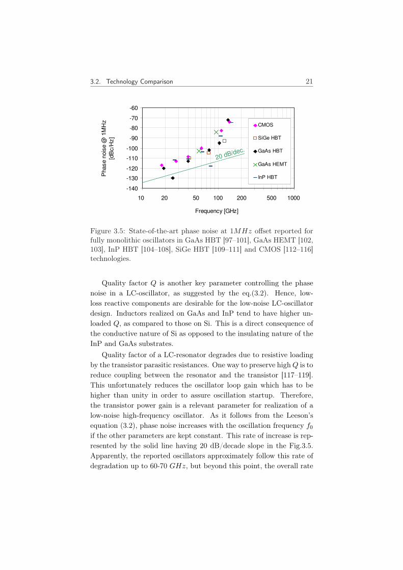
To date, HEMT technologies have been used to demonstrate mm-wave power amplifiers with record output power levels. On the otherhand, the 1/f noise of the HBTs is known to be lower. Hence theHBTs are more attractive for low-phase-noise oscillators as comparedto HEMTs. Fig.3.5 compares the published record phase-noise levelsfor the oscillators implemented in most MMIC technologies. It canbe concluded from the figure that the HBT solutions outperform thefield-effect-transistor solutions across whole frequency range.
3.2. Technology Comparison 21
-140
-130
-120
-110
-100
-90
-80
-70
-60
10 1000
Frequency [GHz]
Phase n
ois
e @
1M
Hz
[dB
c/H
z]
CMOS
SiGe HBT
GaAs HBT
GaAs HEMT
InP HBT
10 20 50 100 200 500 1000
20 dB/dec.
Figure 3.5: State-of-the-art phase noise at 1MHz offset reported forfully monolithic oscillators in GaAs HBT [97–101], GaAs HEMT [102,103], InP HBT [104–108], SiGe HBT [109–111] and CMOS [112–116]technologies.
Quality factor Q is another key parameter controlling the phasenoise in a LC-oscillator, as suggested by the eq.(3.2). Hence, low-loss reactive components are desirable for the low-noise LC-oscillatordesign. Inductors realized on GaAs and InP tend to have higher un-loaded Q, as compared to those on Si. This is a direct consequence ofthe conductive nature of Si as opposed to the insulating nature of theInP and GaAs substrates.
Quality factor of a LC-resonator degrades due to resistive loadingby the transistor parasitic resistances. One way to preserve high Q is toreduce coupling between the resonator and the transistor [117–119].This unfortunately reduces the oscillator loop gain which has to behigher than unity in order to assure oscillation startup. Therefore,the transistor power gain is a relevant parameter for realization of alow-noise high-frequency oscillator. As it follows from the Leeson’sequation (3.2), phase noise increases with the oscillation frequency f0
if the other parameters are kept constant. This rate of increase is rep-resented by the solid line having 20 dB/decade slope in the Fig.3.5.Apparently, the reported oscillators approximately follow this rate ofdegradation up to 60-70 GHz, but beyond this point, the overall rate

22 Chapter 3. MMIC Technologies for Signal Generation
becomes more and more rapid. One likely reason for such trend is thatconductor loss increases and hence Q-factor decreases in frequency dueto the skin effect, since the current flow becomes confined to the con-ductor surface, which depth is proportional to 1/
√f0 [120]. In addi-
tion, lack of high-gain transistors at very high frequencies necessitatesstronger coupling of the resonators to the transistors, which causes theloaded Q to drop in the very high frequency oscillators.
To date, InP HEMT and InP HBT technologies have been usedto demonstrate oscillators operating at highest oscillation frequencies,346 GHz [121] and 311 GHz [122], respectively. The impressive -118dBc/Hz phase noise at 1MHz offset from 80GHz carrier [105] hasbeen demonstrated in InP HBT technology, as depicted in the Fig.3.5.However, to the author’s knowledge, no InP HBT mm-wave quadra-ture oscillators have been demonstrated yet. Low phase-noise QVCOsare preferably constructed by coupling two identical LC-oscillators.Achievement of a high oscillation frequency is impeded by the designcomplexity and additional layout parasitics. Hence, the reported QV-COs are largely limited to 40GHz range [45–49].
From the results presented in this section, it is concluded that InPHBT technology is an interesting candidate for the mm-wave QVCOdesign, and it will be utilized in this work.
3.3 GaN HEMT Technology
The idea behind high electron mobility transistor (HEMT) is to sepa-rate the drift electrons from the dopants in order to obtain high mobil-ity. Schematic cross section of a basic AlGaN/GaN HEMT structureis illustrated in Fig.3.6. The semi-insulating GaN buffer layer grownon a SiC substrate provide good electrical isolation between transis-tors when used in an integrated circuit. The channel region is formedas a two-dimensional electron gas (2DEG) at the interface betweenthe GaN buffer layer and the undoped AlGaN spacer layer [123]. Thehighly doped AlGaN layer supplies the electrons to the channel. Gateelectrode is formed on top of the GaN cap layer. Gate voltage con-trols the electron density in the channel and thereby the drain-sourcecurrent.

3.3. GaN HEMT Technology 23
SiC substrate
GaN buffer
Undoped AlGaN spacer
GaN cap
DrainGateSource
n-doped AlGaN
2-D electron gas
Figure 3.6: Schematic cross section of a basic GaN HEMT structure.
Power MMICs based on GaAs HEMTs are preferably implementedin a via-hole microstrip circuit medium which allows better power han-dling as compared to the coplanar waveguide (CPW) medium. Thevia-holes, which primary purpose is to connect the source terminal toDC- and signal-ground, also contribute to the removal of the gener-ated heat to the back-side metallization. The thermal limitations ofthe coplanar GaAs HEMT amplifiers have been resolved using flip-chip mounting in combination with thermal bumps [26, 124]. On theother hand, excellent thermal conductivity of the SiC substrate en-ables fabrication of coplanar GaN HEMT power MMICs [31,32] withcomparable power performance to those made in microstrip [33–35].
For the design of X-band PA, a GaN HEMT coplanar MMIC pro-cess from Ferdinand Bran Institute für Höchstfrequenztechnik (FBH)has been chosen. Key specifications for the depletion-mode HEMTdevices from this process are presented in the Table 3.2. Si3N4 MIMcapacitors (300 pF/mm2) and NiCr resistors (50 Ω/¤) are available inthe process. The MIM capacitors are adapted for high-voltage circuits.
Parameter ValueGate length × Gate width 0.35 µm × 125 µm
ft/fmax 23/90 GHz
Output power density 4.4 W/mm
IDSS(@VGS = +2V ) 1 A/mm
Table 3.2: Key specifications for the GaN HEMT from FBH’s MMICprocess [125].

24 Chapter 3. MMIC Technologies for Signal Generation
A model of a power HEMT having eight gate fingers comprising atotal periphery of 1 mm has been provided by FBH. The model hasbeen implemented as a symbolic defined device (SDD), an equation-based representation in ADS. In order to check validity of the tran-sistor model under large-signal drive, output-power (POUT ) was mea-sured versus swept input available power (PIN ), and compared to thosegenerated by the model under same bias, drive and loading conditionsat 8GHz. Prior to this, a load impedances for maximum POUT andPAE were determined using a load-pull measurement. In this large-signal measurement, the computer-controlled load-tuner presented awide range of impedances to the transistor, which photo is shown inFig.3.7. The common-source connected transistor was biased at thedrain-source voltage VDS=28V and gate-source voltage VGS=-2.8V .Resulting deep class-AB quiescent drain current was ID=80mA, whichis 8% of a drain-source saturation current IDSS . An input powerPIN=23 dBm was applied to the input, such that large-signal gainof the optimally loaded transistor was compressed by 1 dB below thesmall-signal value. On the input side, the transistor was terminatedfor maximum small-signal gain under the optimal load condition.
G D
Figure 3.7: An 8×125 µm GaN HEMT connected by probes into aload-pull measurement setup. The interdigitated drain and gate fin-gers are combined by the drain and gate combining tapers, respec-tively.

3.3. GaN HEMT Technology 25
Based on the measured POUT and PAE values at various loadimpedances, constant-POUT and a constant-PAE contours are mappedonto a Smith-chart as displayed in the Fig.3.8. Output power or PAEcan be maximized by selecting the corresponding optimum impedanceZOPT as indicated in the figure. Load impedance required for maxi-mum output power in general differs from the impedance maximizingthe gain. Since PAE depends not only on the output power but alsoon the gain, (see eq.(2.2)), the separation between the two ZOPT val-ues is especially pronounced in low-gain devices [126]. The optimumimpedance selected for the power-sweep was calculated as an averageof the two ZOPT values, i.e.
ZOPT = 0.5× [(15 + j30.9) + (18.9 + j23.2)] ' 17 + j27. (3.3)
Measured and modeled POUT vs. PIN curves for the transistorbiased at 80 mA and terminated by ZOPT calculated for that operatingpoint are displayed in the left plot in Fig.3.9. The right plot in Fig.3.9displays the compared powers at higher bias current, 190 mA. Themodel overestimates the saturated output power by around 2 dB underboth bias conditions. Lossy et al. [4] have also observed substantialdegradation of microwave power compared to the expectations basedon DC measurements of FBH GaN HEMTs. This degradation hasbeen ascribed to trapping effects [4].
-1 0 1
ZOPT = 18.9+j23.2
POUT,MAX = 34 dBm
Step = -0.1 dBm
ZOPT = 15 +j30.9
PAEMAX = 42 %
Step = -2 %
Figure 3.8: Constant output power and constant PAE load-pull con-tours for the 8-finger device driven by PIN=23dBm and biased atID=80mA and VDS=28V .

26 Chapter 3. MMIC Technologies for Signal Generation
5 10 15 20 25 3015
20
25
30
35
40
PIN
[dBm]
PO
UT [d
Bm
]
ID
= 80 mA
5 10 15 20 25 3015
20
25
30
35
40
PIN
[dBm]
PO
UT [d
Bm
]
ID
= 190 mA
Figure 3.9: Modeled (-) and measured (o) output power vs. availableinput power for the 8-finger HEMT biased at 28V and terminated by17+j27 load impedance.
The substantial discrepancy between the modeled and measuredpower performance would not allow characterization of the power am-plifier operating under gain compression. Besides the model verifica-tion, the presented large-signal measurements will therefore also servefor the design of the amplifier’s matching circuits. The model wasfortunately capable of reproducing small-signal parameters of the de-vice even at 25 GHz. In order to assess the amplifier performance atvarious terminations at second harmonic frequency, the model will beexploited at moderate power levels before the onset of the compres-sion. The model parasitics will also serve to find an adequate scalingmethod for this 8-finger transistor, in order to predict the behavior ofa 12-finger transistor used for the PA design.
3.4 HBT Technologies
In a conventional npn homojunction bipolar device (BJT) biased underforward active mode, the electrons injected from emitter into the basediffuse across the base to be finally swept into collector by the strongelectric field of the inversely polarized base-collector (B-C) junction[127]. In a heterojunction bipolar transistor (HBT) the emitter is madeof semiconductor material having wider bandgap energy compared tothe base material. The resulting energy band diagram is reproduced

3.4. HBT Technologies 27
in the Fig.3.10 [128]. The additional energy barrier ∆Ev appearing inthe valence band of the B-E heterojunction increases the current gainβ = Ic/Ib by making it difficult for the base holes to cross the junctionand recombine with the electrons in the emitter. In addition, reducedemitter charge improves the speed. The hole-to-electron current ratioacross the heterojunction is given by
(Ih
Ie
)
hetero
=(
Ih
Ie
)
homo
exp(− (∆Eg −∆Ec)
kT
)(3.4)
where the factor before the exponential term is the current ratio ofan equivalent homojunction, ∆Eg = ∆Ec + ∆Ev is the bandgap dif-ference, ∆Ec is the conduction band discontinuity (spike), k is Boltz-mann’s constant and T is the temperature. In the abrupt heterojunc-tion ∆Ec impedes the electron injection into the base, which tend toneutralize the advantage of the barrier in the valence band. This spikein AlGaAs/GaAs HBTs can be eliminated by compositional gradingof the Al-content in the emitter very close to the interface [129].
Base profile in most HBTs is actually compositionally graded. Thiscauses gradual narrowing of the bandgap towards the collector as il-lustrated in the Fig.3.10. The created electric drift-field acceleratesthe electrons, thereby reducing the base transit time. This is anotherattractive feature of the HBT. Two figures of merit (FOMs) character-izing the high frequency capabilities of the transistors are the unity-current-gain frequency ft and maximum oscillation frequency fmax.In order to illustrate the above-mentioned advantages of the hetero-junction effects it is instructive to examine the usual expression forft [130] and fmax [127],
ft =12π
τb + τe + τc +
kT
qIc(Cbe + Cbc)
, (3.5)
fmax =
√ft
8πCbcRb. (3.6)
Here τb, τe and τc are electron transit times through base, emitter andcollector, respectively, Cbe and Cbc are depletion capacitances of thetwo junctions and Rb is the base series resistance.

28 Chapter 3. MMIC Technologies for Signal Generation
emitter base collectorbase
gradedemitter-base
junction
homojunctiontransistor
graded
base
Figure 3.10: Energy band diagram of the HBT biased in forward activemode [128].
Reduction of the τb due to the field-aided transport elevates ft andthereby also fmax. Moreover, reduced base hole current in an HBTopens a possibility to either decrease the emitter doping or to increasethe base doping, while maintaining high β [131]. The benefits of thesetwo actions are:
• The reduced emitter doping cuts down the Cbe, which improvesboth FOMs.
• Increased base doping enhances fmax through reduction of Rb.
To take a full advantage of reduced base transit time in a graded-base HBT, collector transit time should be minimized as well, whichcan be accomplished by increasing a doping in the intrinsic collector.This approach fortunately also postpones the base widening (Kirk-effect) [132] to a higher collector currents, thereby also improving fre-

3.4. HBT Technologies 29
quency response. An important drawback of high collector doping isreduced breakdown voltage.
3.4.1 InP HBT Technology
InP HBT technology developed by Alcatel-Thales III-V laboratory(ATL) was presented in reference [133–135]. During the last decade,the technology has been used to fabricate high-speed integrated cir-cuits for >40 Gbit/s optical transmission systems [133–137].
The HBT epitaxial structure is grown on semi-insulating InP sub-strate. It comprises a low-doped 120nm InP emitter, and 30-50nm
wide InGaAs base with graded indium composition. Doping level inthe base is optimized to maintain a low sheet resistance while keep-ing high current gain. Step-graded collector provides a heterojunctionat the B-C interface and gives a high breakdown voltage required forpower applications.
The HBTs have emitter length of 1.5µm, and available emitterwidths are 3, 6, 10, 15 and 20 µm. Typical performance of the 10 ×1.5 µm2 device are listed in the Table 3.3. For circuit fabrication,transistors are interconnected using vias through polyamide. ThreeTi/Au interconnect metal layers, TaN resistors (50 Ω/¤) and MIMcapacitors (0.36 fF/µm2) are available. It should be noted that ATLhas recently developed a faster, 300GHz ft, process based on reducedemitter length, 0.5 µm [138].
Parameter Value Remarksβ 50 peak value
Peak ft/fmax 170/170GHz @1.5V , 1.5mA/µm2
BVCEO 7V @100µA
Emitter area 10× 1.5µm2
Table 3.3: Key specifications for the ATL’s 10µm InP HBT [133,135].
The design of E-band power amplifier undertaken in this thesis wasbased on the 10×1.5µm2 device. A large-signal UCSD model was pro-vided [11] for use in Agilent ADS. Comparison between the measuredand modeled data is summarized in Fig.3.11. The small inaccuracyin ft fit at 2.5V /20mA will possibly introduce slight uncertainty in

30 Chapter 3. MMIC Technologies for Signal Generation
the small-signal behavior of the PA, which will be biased near thatoperating point. Apart from that, the model is capable of accuratelydescribing behavior of the device. Especially, good consistency is ob-served in the saturation region (low voltage region) of the DC outputcharacteristics, which is of particular importance for prediction of theoutput power under large-signal drive. The shown S-parameters aretaken around peak ft bias point (1.6V , 27mA) and up to 65GHz.
IB = 0….1mA
Forward output
Vce [V]
VCE = 0.9V.1.6V,2.5V
Maximum oscillation frequency
Cutoff frequency
IC [A]
f t [
GH
z]
I C [
mA
]
S21/25
S12x5
S11
S22
f ma
x [
GH
z]
VCE = 0.9V.1.6V,2.5V
IC [A]
Figure 3.11: Measured (o) versus simulated (-) data for the 1.5×10µm2
InP HBT [11].
Another device, used for quadrature oscillator design, has an emit-ter area of 3×1.5µm2. The model provided for this design has beendescribed in [139]. Comparisons between S-parameters, collector-basecapacitance and ft measurements/model reveal globally a good agree-ment. Large-signal verification of the two InP HBT models has notbeen performed.

3.4. HBT Technologies 31
3.4.2 SiGe HBT Technology
In a SiGe based HBT, heterojunctions at base-emitter and base-collectorinterfaces are formed by addition of germanium (Ge) into the base.Linear increase of Ge concentration from B-E towards the B-C junc-tion provides a gradual narrowing of the bandgap as in the case ofthe InP HBT. The resulting field-aided transport leads to improvedtransit time. However, very big improvement is difficult to reach be-cause of the technological need to limit the Ge concentration and/orthickness of the base.
IHP institute provides a BiCMOS process family SG25H that inte-grates carbon-doped SiGe HBT into an advanced 0.25-µm CMOS plat-form [140]. Particularly, SG25H2 is a complementary BiCMOS pro-cess (CBiCMOS) containing npn devices as well as pnp-type bipolartransistors. This state-of-the-art pnp HBT offers peak ft/fmax valuesof 90/120GHz at 2.8V collector-emitter breakdown voltage BVCEO.Device exhibiting highest ft and fmax but lowest breakdown voltagein this process is an npn-type HBT. Key set of electrical parametersfor that device are listed in Table 3.4. Model extraction for the SiGeHBT and evaluation of its performance at 73.5 GHz will be describedin chapter 5.
Parameter Value Remarksβ 200 @Vbe = 0.7V
peak ft/fmax 170/170 GHz @Vce = 1.5V
BVCEO 1.9 V
BVCBO 4.5 V @Ic = 0.1µA
Emitter area 0.21×0.84 µm2
Table 3.4: Key specifications for the npn HBT from the IHP’s SG25H2CBiCMOS process [141].
The schematic cross-section of the npn HBT is shown in Fig.3.12.Highly-doped Si-poly is used to contact intrinsic base and emitterregions resulting in low resistance. Low-resistance of the external sub-collector was obtained by high-dose ion implantation and by lateralshrinking of the device dimensions. This is beneficial for power am-plifier performance since collector resistance limits the voltage swing

32 Chapter 3. MMIC Technologies for Signal Generation
achievable by the device. Low collector resistance also reduces a col-lector charging time that contributes to the the total transit time, asit will be shown later in eq.(5.43).
Complete lateral enclosure of the collector wells by the shallowtrench isolation sidewalls (STI) improves the low-capacitance isolationto the substrate. The absence of deep trench isolation, which is morecommonly used in SiGe HBTs [142,143], improves the heat dissipation[144].
Figure 3.12: Schematic cross-section of the npn HBT structure of theH2 BiCMOS process from IHP [140].

Chapter 4
GaN HEMT X-band PowerAmplifier Design
This chapter will present the design of fully monolithic two-stagehigh-power amplifier based on the coplanar waveguide gallium-nitrideHEMT technology described in the section 3.3.
Peak PAE is usually reached at high input drive level, where signif-icant part of the consumed DC-power is converted into a fundamental-tone power being dissipated in the load. On contrary, increasing thedrive power also increases the degree of nonlinearity. Efficiency andpower capability at high levels of linearity can be improved with ap-propriate circuit design. The performance of the power amplifier isstrongly influenced by the drain bias current ID of the unit tran-sistor cells. The measurements of the power-transistor performancepresented in this chapter will provide a basis for the selection of ID.Dependence of efficiency and gain on input power will by first eval-uated in a one-tone test at different ID values. The intermodulationdistortion of the power device was also measured in a two-tone testwith ID as parameter. Concept of intermodulation distortion, widelyadopted FOM of linearity, will be briefly explained. Measurementsetup and collected results will be discussed.
Another aspect that needs a careful attention is termination of thedevices at higher harmonic frequencies. The harmonic tuning is well-known method of improving the output power and the efficiency of
33

34 Chapter 4. GaN HEMT X-band Power Amplifier Design
a power amplifier [145, 146]. The effects of source and load harmonicimpedances on the voltage and current waveforms and PAE will beinvestigated. The study is based on large-signal model simulations.Most favorable harmonic impedances will be identified and approxi-mate values realized in the amplifier circuit.
In the section 3.3, large-signal measurements of the power HEMTwith gate pitch 50 µm were discussed. The gate pitch determines outerdimensions of the multi-finger device and thereby generated power perchip area. Hence, power devices with reduced gate pitch and sameouter dimensions are desirable. The S-parameters and the optimumload impedance of a 33µm-pitch device will be obtained by scaling themeasured data of the 50µm-pitch device presented in the section 3.3.
The driver stage of the power amplifier consumes the supply powerwithout contributing to the useful output power. It is therefore notsurprising that the two most efficient GaN MMIC results, 44% [31] and35.3% [34], presented previously in the Fig.3.1, contain only one am-plifier stage. Considerations regarding the optimum driver peripherywill be discussed. The amplifier topology and details of the circuit willbe presented. Finally, the amplifier performance will be estimated.
4.1 Bias-Current Selection
The available voltage region of a field-effect transistor spans from theknee region where ID begins to saturate up to the break-down voltageon the ID/VDS characteristics. In order to obtain a high output volt-age swing and resulting high output power, FBH devices are normallybiased at 28 V drain-source voltage [31, 147]. The 28 V bias volt-age was adopted in this work. In this section, the drain bias currentproviding most favorable compromise between efficiency and linearityperformance of the used power HEMTs will be identified. One-tonemeasurements at various bias currents will provide information aboutgain and PAE versus swept input power. Two-tone measurements willprovide a basic insight into intermodulation distortion behavior of thetransistor.
4.1. Bias-Current Selection 35
4.1.1 One-Tone PAE and Gain Considerations
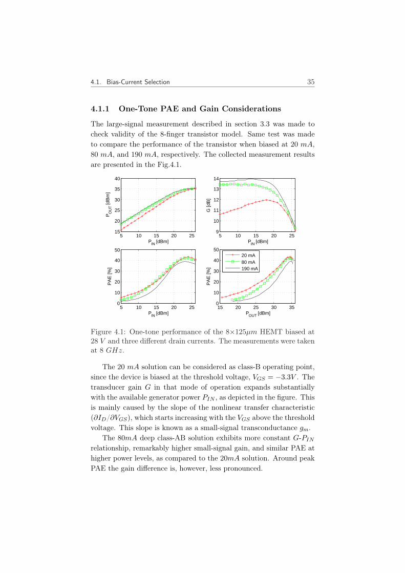
The large-signal measurement described in section 3.3 was made tocheck validity of the 8-finger transistor model. Same test was madeto compare the performance of the transistor when biased at 20 mA,80 mA, and 190 mA, respectively. The collected measurement resultsare presented in the Fig.4.1.
5 10 15 20 2515
20
25
30
35
40
PIN [dBm]
PO
UT [d
Bm
]
5 10 15 20 259
10
11
12
13
14
PIN [dBm]
G [d
B]
5 10 15 20 250
10
20
30
40
50
PIN [dBm]
PA
E [%
]
15 20 25 30 350
10
20
30
40
50
POUT [dBm]
PA
E [%
]
20 mA80 mA190 mA
Figure 4.1: One-tone performance of the 8×125µm HEMT biased at28 V and three different drain currents. The measurements were takenat 8 GHz.
The 20 mA solution can be considered as class-B operating point,since the device is biased at the threshold voltage, VGS = −3.3V . Thetransducer gain G in that mode of operation expands substantiallywith the available generator power PIN , as depicted in the figure. Thisis mainly caused by the slope of the nonlinear transfer characteristic(∂ID/∂VGS), which starts increasing with the VGS above the thresholdvoltage. This slope is known as a small-signal transconductance gm.
The 80mA deep class-AB solution exhibits more constant G-PIN
relationship, remarkably higher small-signal gain, and similar PAE athigher power levels, as compared to the 20mA solution. Around peakPAE the gain difference is, however, less pronounced.

36 Chapter 4. GaN HEMT X-band Power Amplifier Design
The gain can be only slightly improved if the drain current is fur-ther increased to 190 mA. At the same time, the 190 mA solutionexhibits inferior PAE performance, as demonstrated in the two bot-tom plots of Fig.4.1. This is especially pronounced at moderate andlower power levels, since high bias current is flowing through the deviceregardless of the applied PIN or output power POUT .
From the discussion above it can be concluded that low bias cur-rents, 20 and 80mA, provides more favorable compromise betweenhigh gain and high PAE performance, as compared to the 190 mA
current.
4.1.2 Intermodulation Distortion
An amplitude modulated carrier signal gets spectral components stem-ming from the baseband signal below and above the carrier frequency[148]. When the carrier is suppressed the equation for such signalreads
VIN = C [cosωAt + cosωBt] . (4.1)
In this example, (ωA − ωB) is the angular frequency of the basebandsignal modulating the carrier at the center frequency (ωA + ωB)/2.Time-domain waveform of the two-tone signal at the input of a deviceis illustrated in the Fig.4.2.
2C
time
freq.
C
VIN[V]
A B A B
2A-
B2
B-
A
freq.
VIN[V]
VIN
VOUT
VOUT
[V]
Figure 4.2: Two-tone time domain voltage waveform and frequencycomponents at input and output of a power amplifier.
Being a nonlinear circuit, a power amplifier driven by the two-tonesignal generates additional frequency components. The third orderintermodulation products (IM3) at sideband frequencies (2ωA − ωB)

4.1. Bias-Current Selection 37
and (2ωB − ωA) [149] are of particular interest for communication sys-tems since they cause bit error rate degradation [150]. The frequencyspectra at the amplifier output is indicated in the Fig.4.2. Third orderintermodulation distortion (IMD3) is often used as a linearity measureof a PA. It is defined as a ratio between the single-carrier output power(either at ωA or at ωB) to the power of the single IM3 product.
Two-Tone Measurement Setup
Two-tone measurements were carried out to understand basic linearitycharacteristics of the 8-finger power HEMT biased at three differentcurrents. The intermodulation distortion was measured in the two-tone test setup illustrated in Fig.4.3. The spectral contents at thedevice output were monitored by the Agilent Performance SpectrumAnalyzer (PSA). The test signal composed of two tones separated by10 MHz around 2 GHz was generated by the Agilent PerformanceSignal Generator (PSG). To obtain sufficient drive level the signalwas subsequently amplified by the power amplifier (PA), which unfor-tunately also generated its own IM3 products. Cancelation of thesefrequency components required predistortion of the PSG signal. Thislinearization of the PA output was carried out using the Agilent Sig-nal Studio software installed on the PC. In the calibration processthe software collected the distortion data from the Performance Spec-trum Analyzer (PSA) driven by the PA and iteratively computed aparameter controlling the predistortion of the PSG.
VDS
GS
GG
SGPA
Two-tone
PSG
PC
PSAAttenuator
TunerTuner
VGS
Figure 4.3: Two-tone measurement setup.
Input power sweep was realized through the computer controlledattenuator as indicated. Thus the PA was driven at constant powerlevel, and a single predistortion parameter was valid across the entire

38 Chapter 4. GaN HEMT X-band Power Amplifier Design
power range. The mechanical tuners applied at the transistor inputand output provided maximum gain and maximum output power, re-spectively. The transistor was mounted on a copper flange. It wasconnected to the power supplies through the bias-Ts as illustrated.Losses in the measurement equipment at the device output were sub-tracted from the measured results.
Two-Tone Measurement Results
The intermodulation distortion data monitored on the PSA are plottedin the Fig.4.4. Most linear operation was exhibited at highest biascurrent 190 mA under low-power operation, since the device operatedat most linear part of the ID-VGS characteristic.
At higher power range, low bias currents tend to provide lowestIMD3 as indicated. As the bias current reduces from the 190 mA, a’valley’ start to appear in the IMD3 plot at high-power levels. Theoccurrence of the high-power ’valley’ in the vicinity of the class-B biaspoint has also been observed by other authors [151–153]. This propertyof HEMT devices has been analyzed and explained as opposite phaseinteractions of various intermodulation products [153].
POUT
[dBm]
IMD
3 [
dB
c]
13 mA
-10
-20
-30
-40
-50
-60
15 20 25 30 35
190 mA
80 mA
P1dB
Figure 4.4: Measured IMD3 versus output power (each carrier) for a1mm HEMT at 2GHZ center frequency, 10MHz tone spacing andVDS=28V .
As suggested by the curves in the Fig.4.4, a penalty of reducing thecurrent below 80mA could be an excessive distortion. Data-sheets forcommercial solid-state [154–156] and TWT [157] high-power amplifiers

4.2. Device Scaling 39
for satellite uplink applications in the 7.9-8.4GHz band, often reportintermodulation distortion of -25 dBc. As it appears in the Fig.4.4,as the current is reduced from 190 to 80 mA, the point where IMD3falls to -25 dBc is pushed up 1 dB on the POUT scale.
In the single tone measurements presented in the Fig.4.1, the 1mm
device, biased at 80 mA, reached 1dB gain compression at outputpower of 33.4 dBm. When excited by two tones, the device reached1dB compression at around 28dBm, that is, almost 6dB lower outputpower for each carrier. This power level is indicated as P1dB in theFig.4.4. According to the figure, at the power levels above 27 dBm
(1dB back-off), the 80mA operating point provides best linearity. Atthe same time, for any power level up to 29dBm (2dB compressionpoint) the IMD3 is better than -30 dBc.
The 80mA/mm current results in improved linearity at high powerlevels. Limitations in the setup allowed the measurements to be doneonly up to 2 GHz, which is fairly below the 8 GHz where the transis-tors will operate in the amplifier. As mentioned, however, the othergroups have observed similar IMD3 behavior of GaN HEMTs biasednear class-B. This bias condition also offered high gain and high PAEin the one-tone measurements. It was therefore decided to adopt the80mA/mm operating condition for the transistors used in this MMICdesign.
4.2 Device Scaling
A HEMT device with reduced pitch and unchanged number of gatefingers exhibits reduced outer width, which saves the chip area. Apartfrom being cost-effective, such a solution requires an output combin-ing network with reduced line length and consequently lower powerloss and higher efficiency. The 8-finger device discussed until nowexhibits 50µm gate-to-gate spacing (gate pitch). Another availabledevice had 12 gate fingers, 33µm gate pitch, and same dimensions ofthe tapers combining the gate and drain fingers, as the 8-finger device(see Fig.3.7). Thanks to the larger total periphery, this device offeredincreased output power at same chip size for the designed PA.

40 Chapter 4. GaN HEMT X-band Power Amplifier Design
S-parameters and load-pull measurements of the 12-finger/33µm
HEMT were not available. Scaling the 8-finger device data was there-fore attempted. An appropriate scaling trend was derived by com-paring the measured S-parameters of 12-finger and 18-finger deviceshaving a gate pitch 50 and 33 µm, respectively. The outer devicewidth of these two devices was 50% larger as compared to the widthof the 8-finger device. The 18-finger device generated about 1.8 dB
(or ∼1.5×) higher power than the 12-finger device due to the 50%larger periphery. Similar improvement was therefore expected fromthe attempted 8-to-12 finger scaling.
4.2.1 Scaling Method
Equivalent circuit showing parasitic elements of the transistor struc-ture is depicted in Fig.4.5 (left). Values of the passive elements takenfrom the device model are summarized in Table 4.1. Elements CTG,LTG, and CTD, LTD represent the parasitic effects of the two tapersconnected to the gate and drain side, respectively. Fig.4.5 (right) il-lustrates schematic cross section of the HEMT interdigitated structureincluding the gate and drain fingers as well as the airbridge connectingthe source fingers. The effective airbridge inductance LS was assumednot to scale, since the airbridge length was unchanged.
CDS
RD
LS
LTD
CTD
LTG
CTG
Yint
G S G D G S G
Gate pitch
Figure 4.5: Left: Equivalent circuit of the HEMT including the taperparasitics. Right: part of a schematic cross section showing gate,source and drain fingers.
A 4-step procedure for scaling the 12-finger to the 18-finger de-vice was carried out by optimizing RD and CDS values as describedbelow. The RD and CDS were optimized to fit the scaled and mea-sured S-parameters of the 18-finger device. Increasing the number ofthe gate fingers by the scaling factor 1.5 (=18/12) while keeping the

4.2. Device Scaling 41
total device width and finger spacing constant, slightly reduces thetotal width of the drain fingers. The total drain access resistance RD
is therefore expected to increase in stead of being reduced 1.5 times.The scaling trend is less obvious for the drain source capacitance CDS ,since the total drain area and associated parallel plate capacitance tothe airbridge diminish, but the total fringing capacitance increases dueto the increased number of drain fingers.
Step 1: A small-signal admittance matrix Yint,12 representing theintrinsic 12-finger HEMT device was firstly calculated by subtractingthe contributions of the passive elements to the measured Y-parametermatrix of the entire device, Ymeas,12. The calculation was accom-plished through the eq.(4.2-4.5).
Yd1 = Ymeas,12 −[jωCTG 0
0 jωCTD
](4.2)
Yd2 =
Y −1
d1 −[jωLTG 0
0 RD + jωLTD
]−1
(4.3)
Yd3 = Yd2 −[0 00 jωCDS
](4.4)
Yint,12 =[Y −1
d3 − jωLS
]−1. (4.5)
.Step 2: Intrinsic admittance matrix of the 18-finger device was
then calculated by linear scaling as Yint,18=1.5×Yint,12.Step 3: The elements CDS , and RD of the 18-finger device were
scaled using the optimization factors kC and kR as
CDS,18 = kCCDS,12 (4.6)
RD,18 = kRRD,12. (4.7)
Step 4: Finally, the admittance matrix of the 18-finger device wascalculated by attaching CDS,18 and RD,18, as well as the remainingnon-scaled passives of the structure in the Fig.4.5 to the Yint,18.

42 Chapter 4. GaN HEMT X-band Power Amplifier Design
By optimization of the empirical factors kC and kR the modeledS-parameters of the entire 18-finger device were fitted to the measuredones. The most representative values were found to be kC = 1.25, andkR = 1.07. The scaled parasitic drain resistance increased slightly, asexpected. Note that, if the gate-pitch reduction was disregarded inthe scaling procedure, and only the number of fingers was considered,the two scaling factors would equal 1.5 and 1/1.5, respectively.
Good agreement was obtained between the scaled and the mea-sured S-parameters of the 18-finger device. Most apparent discrep-ancy was observed in the S22 magnitude, which was highly dependenton CDS and RD elements. In Fig.4.6, the ’Simple 1.5× scaling’ curverepresents the intrinsic device scaled 1.5 times, inclusive CDS andRD. Using the ’Correct scaling’ method described above, the agree-ment between the measured and the modeled |S22| improves. Slightimprovement was also observed in |S12| fit (not shown).
Simple 1.5x scaling
Correct 1.5x scaling
Measured
ph
ase
(S2
2 ) [de
g]
ma
g (
S2
2)
0.65
0.70
0.75
0.60
0.80
Frequency [GHz]
6
140
150
160
170
130
180
10 14 18 22 26
Figure 4.6: Measured and modeled S22 for the 8-finger device.
Fingers / P itch CTG LTG CTD LTD RD CDS LS
[fF ] [pH] [fF ] [pH] [Ω] [fF ] [pH]12 / 50 µm 121 134 121 130 1.14 362 7.6(not scaled)8 / 50 µm 91 126 91 123 1.54 250 2.2
(not scaled)12 / 33 µm 91 126 91 123 1.44 312 2.2
(scaled)
Table 4.1: Parasitic element values for the GaN HEMTs.

4.3. Second-Harmonic Tuning 43
4.2.2 Results of the Scaling
Finally, using the scaling method with kC and kR calculated above,S-parameter matrix of the 12-finger device with 33µm pitch was pre-dicted by scaling the 8-finger device with 50µm pitch. The obtainedCDS and RD are presented in the Table 4.1.
Optimum load impedance of the 8-finger HEMT, ZOPT = 17+j27Ω, found in the load-pull measurement described in section 3.3, wasscaled in the same manner to obtain ZOPT of the 12-finger/33µm
device. The optimum impedance at 8 GHz became 13 + j17 Ω.
4.3 Second-Harmonic Tuning
High efficiency power amplifier design requires proper device termi-nation not only at fundamental frequency but also at higher orderharmonics. By applying adequate harmonic terminations, the outputvoltage and current waveforms can be shaped such that the powerdissipated in the device is minimized. Aiming at high efficiency, har-monically tuned linear microwave SSPAs often employ lowest possibleload impedance at second harmonic [146, 158–160]. This at the sametime reduces the harmonic level at the output, and prevents the dissi-pation of the 2nd harmonic energy in the load.
An ideal parallel-tuned amplifier provides a short for higher orderharmonics at the output. This results in a sinusoidal drain-sourcevoltage and puls-shaped drain-current [161]. Theoretical limit for thedrain efficiency of a parallel tuned amplifier biased in class-B is 78.5%,before the onset of the current clipping. A fully monolithic 5-6GHz
GaAs FET amplifier showed 70% PAE [146]. Low output impedanceswere realized at both 2nd and 3rd harmonics using a short-circuitedmicrostrip stubs near the transistor drain.
An important aspect concerning harmonic tuning approach is thegenerator impedance presented to the gate at higher harmonics. Theeffect of input harmonic terminations on GaAs based power-pHEMTperformance at 5 GHz have been investigated in [162]. It has beenfound that the non-linear effect of CGS can distort the driving volt-age waveform and in turn the ideally half-sinusoidal output current
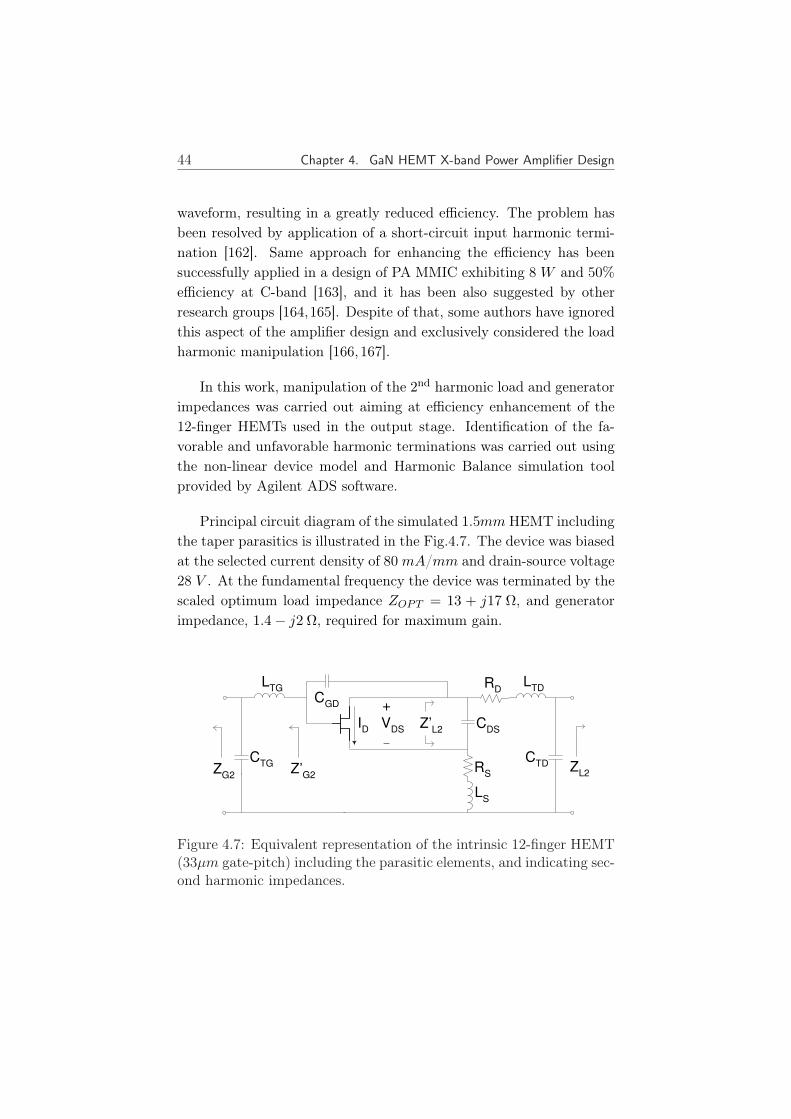
44 Chapter 4. GaN HEMT X-band Power Amplifier Design
waveform, resulting in a greatly reduced efficiency. The problem hasbeen resolved by application of a short-circuit input harmonic termi-nation [162]. Same approach for enhancing the efficiency has beensuccessfully applied in a design of PA MMIC exhibiting 8 W and 50%efficiency at C-band [163], and it has been also suggested by otherresearch groups [164,165]. Despite of that, some authors have ignoredthis aspect of the amplifier design and exclusively considered the loadharmonic manipulation [166,167].
In this work, manipulation of the 2nd harmonic load and generatorimpedances was carried out aiming at efficiency enhancement of the12-finger HEMTs used in the output stage. Identification of the fa-vorable and unfavorable harmonic terminations was carried out usingthe non-linear device model and Harmonic Balance simulation toolprovided by Agilent ADS software.
Principal circuit diagram of the simulated 1.5mm HEMT includingthe taper parasitics is illustrated in the Fig.4.7. The device was biasedat the selected current density of 80 mA/mm and drain-source voltage28 V . At the fundamental frequency the device was terminated by thescaled optimum load impedance ZOPT = 13 + j17 Ω, and generatorimpedance, 1.4− j2 Ω, required for maximum gain.
CDS
LS
CTD
LTG
CTG
Z’G2
ZG2
ZL2
Z’L2
ID
+
_
VDS
CGD
LTDR
D
RS
Figure 4.7: Equivalent representation of the intrinsic 12-finger HEMT(33µm gate-pitch) including the parasitic elements, and indicating sec-ond harmonic impedances.

4.3. Second-Harmonic Tuning 45
4.3.1 Parallel-Tuning Case: Shorted Second Harmonic
As a starting point for the investigation, the generator impedanceZG2 = −j14 Ω and the load impedance ZL2 = −j15 Ω were appliedat the second harmonic frequency 16 GHz. The chosen ZG2 providesshort-circuit seen from the intrinsic gate terminal, i.e. Z
′G2 = 0. The
chosen ZL2 assures low impedance across the drain-source terminals ofthe intrinsic device, Z
′L2 = 2Ω. This is only an approximation to the
short circuit, due to the finite source and drain resistances, RS andRD, respectively. The two resistors actually dissipate around 11% ofthe total fundamental output power POUT . In an ideal parallel tunedamplifier this would cause the drain efficiency to drop from 78.5% toaround 70%.
Simulation was performed at 8 GHz and 20 dBm input poweryielding POUT of 33.2 dBm. This power corresponds to 2dB outputback-off1, when the measured P1dB is taken as the reference. Fig.4.8shows the load trajectory and time waveforms of the intrinsic drain-source voltage VDS and the intrinsic drain current ID. Second har-monic control constrains the output voltage to by nearly a sinusoidat the fundamental frequency. Current pulses occur at the instantswhere the voltage is low, as required by the high-efficiency concept.
I D [A
]
VDS
[V] Time [ps]
I D [A
] VD
S [V]
0
0.2
0.4
0.6
0.0
0.8
10 20 30 40 50 60
0.5
0.0
1.0
50 100 150 2000 250
30
0
60
Figure 4.8: Parallel tuned intrinsic HEMT terminated by ZG2 =−j14 Ω and ZL2 = −j15 Ω at the extrinsic gate and drain, respec-tively. Left: load trajectory. Right: time-domain waveforms. VDS
and ID are indicated in the Fig.4.7.
1The 2dB output back-off refers to the POUT which is 2 dB below the POUT in1dB compression.

46 Chapter 4. GaN HEMT X-band Power Amplifier Design
4.3.2 Impact of Third and Higher Order Harmonics
In this work, second harmonic control of the generator and the loadimpedance was performed. The 3rd and higher order harmonics werenot considered due to the reasons explained below. They were termi-nated by 50 Ω in all the presented simulations.
In the parallel tuned amplifier described above, the 3rd harmoniccontent of ID stayed at least 17 dB below the 2nd harmonic at funda-mental power levels ranging up to 2dB output back-off. Consequently,the voltage and current waveform shapes were mostly dependent onthe 2nd harmonic terminations. By modification of the generator andload impedances at 3rd harmonic frequency, only a small change inPAE was observed, ±0.7%.
The 3rd harmonic tuning became increasingly important as ZG2
and ZL2 moved away from the values required for parallel tuning.However, up to the 2dB back-off it was not possible to obtain higherPAE than that obtained by shorting the 2nd harmonic.
At higher power, beyond 2dB compression level, larger change inPAE (up to ±2.8%), was possible due to rapid increase of 3rd harmoniccontent of the drain current. Creation of an open circuit for the 3rd
harmonic at the intrinsic device terminals is actually a way to a class-Foperation [168]. Second harmonic is shorted as in the parallel-tuningcase. Taking the advantage of a square-like VDS waveform, class-Ftuning offers larger POUT and PAE as compared to the parallel-tuningcase. Since the class-F operation required significant gain compressionto generate the 3rd harmonic output current, the intermodulation dis-tortion would have degraded. Moreover, the model inaccuracy in thecompression regime would not allow reliable harmonic control.
Finally it should be mentioned that the 4th and 5th harmonics hadeven less impact on the PAE as compared to the 3rd harmonic.
4.3.3 Other important Cases
Conclusions presented in following were drawn while tuning the 2nd
harmonic impedances ZG2 and ZL2 around the two start-values deter-mined in the parallel tuning approach, as described above. Again, theresults are based on the input power level of 20 dBm.
4.3. Second-Harmonic Tuning 47
• ZG2 values in the vicinity of −j14 Ω assuring nearly a shortcircuit seen by the transistor gate indeed maximize the PAE.The exact optimum value of ZG2 actually ranged between−j12Ωand −j16 Ω, depending on the chosen ZL2.
• Generator second harmonic impedance value of −j6Ω tunes outthe input capacitance at 2nd harmonic frequency. Resulting VGS
waveform gets distorted and ID pulses broaden as depicted in theFig.4.9 (left plot). This causes excessive power consumption inthe device and deteriorates the PAE. Fig.4.10 illustrates the loadtrajectory and PAE simulated for this case, denoted as ’WorstZG2’. Load impedance ZL2 was kept at the original value forparallel-tuning, −j15 Ω. As it appears from the Fig.4.10 (rightplot), the efficiency is highly dependent on the second harmonicimpedance at the transistor input.
• The PAE degradation is also caused by small positive values ofZL2, which tend to tune out the capacitive load presented atthe intrinsic device output. The case denoted as ’Worst ZL2’in the Fig.4.9 (middle plot) and Fig.4.10 corresponds to ZL2 ofj7 Ω, while ZG2 was kept at the original value, −j14 Ω, used inthe parallel tuning example above. Load impedance Z
′L2 seen
by the intrinsic transistor becomes high and real, around 100 Ω,and introduces strong 2nd harmonic component in the VDS . Thiscomponent is 90 out of phase with the fundamental one.
• On the other hand, moving the ZL2 reactance in a negative di-rection from the start value of −j15 would not tune out thecapacitive output impedance. This direction of change is there-fore expected to be less detrimental. In fact, an improvement of1.5% in PAE was obtained as ZL2 moved towards −j∞ Ω. Inthis case Z
′L2 changed from 2 Ω to (1−j14) Ω. The shape of the
load trajectory for that solution, denoted as ’Optimum’ in theFig.4.10 (left plot), somewhat approximates that of the paralleltuned amplifier.
Obviously, the lowest possible |Z ′L2| (2Ω) does not maximize the
efficiency of the investigated GaN HEMT. This is believed to be

48 Chapter 4. GaN HEMT X-band Power Amplifier Design
caused by the parasitic effects in the transistor. Namely, whenCGD and RD were set to zero, and optimization was repeated,the optimum impedance Z
′L2 moved back near 0 Ω. The shift
of the optimum Z′L2 towards negative reactive values does not
seem to be caused by the 3rd and higher order harmonics.
Time [ps]
I D [
A]
VD
S [V]I D
[A
]
VD
S [V]
VD
S [V]I D
[A
]
Time [ps]Time [ps]
ZG2
=-j6, ZL2
=j15 ZG2
=-j14, ZL2
=7 ZG2
=-j14, ZL2
=-inf
Worst ZG2
case: Worst ZL2
case: Optimum case:
0.2
0.4
0.6
0.0
0.8
20
30
40
10
50
0.2
0.4
0.6
0.0
0.8
10
20
30
40
0
50
0.2
0.4
0.6
0.0
0.8
20
30
40
10
50
1000 200100 2000100 2000
Figure 4.9: Time domain waveforms of the intrinsic device at threedifferent 2nd harmonic terminations and PIN=20dBm.
PIN
[dBm]
PA
E [%
]
I D [m
A]
VDS
[V]
10 20 30 400 50
0.1
0.2
0.3
0.4
0.5
0.6
0.7
0.0
0.8
15 20 2510 30
20
40
0
60Optimum
Worst ZL2
Achieved
Worst ZG2
Figure 4.10: Simulated results for various 2nd harmonic terminationsproviding optimum and worst PAE together with the achieved result.Left: Load trajectories at PIN=20dBm Right: Power added efficiencyversus input power.
Presence of the CDS and CGD at the intrinsic drain significantlysimplifies implementation of the harmonic load. In high-power mi-

4.3. Second-Harmonic Tuning 49
crowave amplifiers employing large-periphery GaN HEMTs, very low2nd harmonic load impedance can otherwise be difficult to realize be-cause of the losses in the matching circuits [167]. Beneficial effectof a large CDS providing low reactance for the harmonics is well-known [169]. Serious drawback of an excessive CDS is that the 50Ωload needs to be transformed to a low optimum load impedance at thefundamental frequency. This increases the loss in the matching circuitand impedes the wideband operation [169]. Moreover, bandwidth re-duction also arises from the fact that the CDS increases the qualityfactor Q of the transistor output impedance. In fact, higher-Q cir-cuits are intrinsically harder to match then are lower-Q circuits [120].Simulations of the transistor circuit from the Fig.4.7 reveal howeverthat CGD also have a pronounced effect on the fundamental loadimpedance. Namely, the optimal impedance (13+j17) Ω transformedback through the drain taper and CDS is found to be (33+j23)Ω. Theoptimum impedance seen by the intrinsic device, however, is real andrelatively high, 53 Ω.
4.3.4 Realized Second Harmonic Impedances
The achieved second harmonic impedances and PAE for the four tran-sistors in the output stage are as presented in following.
Load 2nd harmonic impedance, ZL2
As mentioned before, the optimum second harmonic impedance pre-sented to the drain terminal turned out to be −j∞ Ω. In fact, anysufficiently high |ZL2| would have similar effect on the transistor effi-ciency. In the realized power amplifier presented later in this chapter,the achieved ZL2 seen from the device output became (100+j290) Ω.
Source 2nd harmonic impedance, ZS2
The results presented in the Fig.4.10 reveal that the input side ofthe transistor is even more critical then the load side with respect to2nd harmonic manipulation. Low 2nd harmonic impedance presentedto the intrinsic gate, also implies a low real part of the Z
′G2. As

50 Chapter 4. GaN HEMT X-band Power Amplifier Design
mentioned, the optimal and undesirable reactances are −j16 Ω and−j6 Ω, respectively. The achieved ZG2 was (3−j19) Ω, providing aj3Ω additional safety margin for the generator reactance. The intrinsicZ′G2 became (2.5−j3) Ω.Simulated results for this achieved combination of ZG2 and ZL2
are denoted as ’Achieved’ in the Fig.4.10. The load trajectory andPAE approximate the ’Optimum’ curves.
4.4 Circuit Design
Block-diagram of the designed two-stage power amplifier is illustratedin Fig.4.11. The unit-cell transistors were biased in deep class-AB cur-rent density of 80 mA/mm, where high efficiency and low IMD3 weremeasured. Drain and gate bias voltages are VDD1 = VDD2 = 28Vand VGG1 = VGG2 = −2.8V , respectively. Output matching net-work serves to combine the output signal of the power stage transis-tors. At the same time it provides optimum load impedance to thesetransistors. Similarly, the interstage matching circuit transforms theinput impedance of the power stage HEMTs into the optimum loadimpedance for the driver transistor. It also serves to distribute thedriver output signal equally among the power stage transistors. Inputmatching circuit transforms the input impedance of the driver tran-sistor to the 50Ω generator for minimum return loss. Aiming at highPAE, the output and interstage matching circuits provide the nearly-optimal 2nd harmonic impedances to the power stage transistors, asmentioned in the section 4.3.4.
50-generator
Output
matching
/
power
combiners
18 x
125 m
Interstage
matching
/
power
deviders
50-load
Inputmatching
VG2V
DDV
G1 VDD
12 x
125 m
12 x
125 m
12 x
125 m
12 x
125 m
Figure 4.11: Principal block diagram of the realized power amplifier.

4.4. Circuit Design 51
Premature saturation of the driver HEMT could limit the outputpower and also cause a distortion. To avoid this, the driver output pe-riphery should be sufficiently large. Unfortunately, very large drivertransistor consumes excessive DC power resulting in reduced PAE.Ratio between the driver periphery (18 fingers) to the periphery ofthe power stage (48 fingers) is 1/2.7, according to the number of fin-gers indicated in the Fig.4.11. State-of-the-art GaN HEMT monolithicX-band power amplifiers [31–36,170, 171] exhibit periphery ratios be-tween 1/4.5 and 1/2. From this point of view, the chosen peripheryratio, 1/2.7, can be considered as ’non-aggressive’. It will be shownin section 4.5 that the driver stage operates in ∼ 5.6dB output back-off while the power stage is in 1dB compression. This assures linearperformance and provides a safety margin for the driver. If the 12-finger driver was used in stead, the periphery ratio would have been1/4, and the driver back-off would have dropped to 3.9dB. The pre-dicted PAE would have increased from 29.2% to 30.4%, according tothe estimation described in section 4.5.
Diagram and layout of the amplifier circuit are shown in Fig.4.12and Fig.4.13, respectively. Component values are summarized in theAppendix A. The size of the submitted chip, 3×4mm2, is in the rangeof the state-of-the-art solutions [32–35].
Coplanar transmission lines of the matching/combining networksare represented by the thick lines in the circuit diagram. The draincurrent is supplied through the stubs, which electrical length is around45 at 8 GHz. Since the stubs are AC-shorted by the decoupling ca-pacitors, they act as shunting inductors in the matching circuits. Theshunting capacitors C12, C14 and C17, however, are most importantfor the impedance transformation. The C2 capacitor placed close tothe input of each power stage transistor provides nearly the optimumsecond harmonic impedance to these transistors, which eases the op-timization of the interstage matching circuit elements.
High device gain at low frequencies necessitates use of the resistiveloading in the circuit to prevent parasitic oscillations. Rollet’s stabilityfactor K of the amplifier stages devices are lower than 1 around 3GHz,which implies potential instability [172]. Series connected resistor andcapacitor between gate and drain eliminates this problem.

52 Chapter 4. GaN HEMT X-band Power Amplifier Design
50-Ohm
load
50-Ohm
generator
VDD2
VGG2
VGG1
VDD1
VDD2
VGG2VDD1
C1
C2
C3
C4
C5
C6
C7
C8
C9
C10
C12
C17
C14
C13
C11
C15C
16
R1
R2
R3
R4
R5
R6
R7
R8
L1
R2
C2
Figure 4.12: Circuit diagram of the power amplifier. Component val-ues are identical in the two circuit half-parts symmetrical around hor-izontal center axis.
Input impedance of the optimally matched driver transistor is only(1.4+j4) Ω. This impedance has to be transformed to 50 Ω for min-imum input return loss. As mentioned earlier, a high transforma-tion ratio hampers the design of wideband matching circuits. Outputimpedances of the devices are order of magnitude higher as comparedto their input impedances. The total amplifier bandwidth is there-fore mainly determined by the input and interstage matching circuitsrather than the output matching circuit. By introducing losses in thetwo matching circuits, the amplifier’s 1dB bandwidth was extendedfrom around 250 MHz to 500 MHz. Resistor R5 terminated by thedecoupling capacitor C4 in the gate biasing path of the driver tran-sistor dissipates the signal power at the fundamental frequency. Am-plifier’s power gain reduces around 2dB due to the action of the R5.Same approach was applied in the interstage matching network, wheregain reduction due to R4 was 1 dB.

4.4. Circuit Design 53
C2
Figure 4.13: Layout of the developed power amplifier MMIC (chip sizeis 3×4mm2).
Decoupling capacitor C3 in the gate biasing network of the powerstage provides nearly a short circuit at 8 GHz. Its impedance ishowever non-negligible in lower GHz range. The R6-C5 section createsan additional lossy path seen by the matching circuit in the lower GHz
range. This further improves the stability at lower frequencies. Gatebiasing network of the driver transistor is based on same approach.
Possible development of odd-mode oscillations within each of thetwo transistor pairs of the power stage was prevented by connectingthe gates by R2 resistors. Similarly, odd-mode oscillations which canexist between the transistor pairs are prevented by resistor R3.
The maximum current that can flow through a cross section ofa coplanar center-conductor limits the use of coplanar lines for high-power amplifier design. The two stubs feeding the drain current tothe power stage transistors each carry a maximum current of 0.8A,when the amplifier is driven into saturation. This current correspondsto around 70% of the maximum current flow capacity, above whichelectron migration starts to occur. The distance between the padsin the shown layout is compatible with the standard 150µm-pitch

54 Chapter 4. GaN HEMT X-band Power Amplifier Design
test probes/needles. The pads were made sufficiently large for wire-bonding. The input and the output signal pads were made sufficientlywide to accommodate two bonding wires placed in parallel, which willreduce the parasitic inductances.
4.5 Predicted Performance
Models of the passive structures for circuit simulations in ADS wereprovided by FBH. S-parameter of the inductors and combiners werebased on electromagnetic simulations. Analytical scalable models ofthe coplanar elements were available in the design kit. These encom-passes MIM capacitors, coplanar lines and coplanar discontinuitiessuch as T-junctions, 90-bends and underpasses.
Fig.4.14 shows the simulated small-signal S-parameters for the de-veloped PA. Simulated S21 drops by 1 dB at 7.7 GHz and 8.4 GHz.In this frequency range, |S11| and |S22| return losses, are better than8 and 7 dB, respectively.
7.5 8.0 8.5 9.07.0 9.5
10.0
15.0
20.0
5.0
25.0
-30
-20
-10
-40
0
Frequency [GHz]
S2
1 [
dB
]S
11 , S
22 [d
B]
S21
S11
S22
Figure 4.14: Simulated S-parameters of the power amplifier.
As indicated before, the transistor model was not capable to accu-rately predict the behavior of the device at high power levels. Anal-ysis presented below estimates the achieved PAE and output powercapability, based on the measured and scaled transistor data and thesmall-signal simulations of the amplifier circuit at 8 GHz. Impact ofharmonic tuning is not considered. The estimated results are after-wards compared to the simulated ones.

4.5. Predicted Performance 55
In the power-sweep test, the 8-finger device biased at 80 mA/mm
delivered 33.4 dBm in 1dB compression. The scaled 12-finger power-stage device is expected to produce 1.8 dB higher power as mentionedin the section 4.2. Four of such devices together deliver 6 dB morepower. Total power delivered to the output matching circuit becomes
Po2 = 33.4 + 1.8 + 6 = 41.2[dBm] (4.8)
Simulated power loss in the output matching circuit is 0.8 dB. Thepredicted power delivered by the amplifier to the 50Ω load becomes
POUT = Po2 − 0.8 = 40.4[dBm] = 11[W ]. (4.9)
Calculated in same manner, saturated output power becomes 42.5dB.
Simulated power gain of the interstage matching circuit was−2.5dB.Measured input power for the 8-finger HEMT was 21dBm in 1dB
compression. Power delivered by the driver transistor can now beestimated by applying the scaling rules as in the eq.(4.8),
Po1 = 21 + 1.8 + 6 + 2.5 = 31.3[dBm]. (4.10)
Based on the the estimated output powers and periphery ratio1/2.7, the difference between the output power densities of the tworespective stages can also be found,
Po2 − Po1 + 10 log10(1/2.7) = 41.2− 31.3− 4.3 = 5.6[dBm]. (4.11)
The calculated power density ratio indicate that the driver operatesat 5.6 dB lower power density as compared to the power stage, whenthe later is in 1dB compression. Hence the driver is in 5.6dB back-off.
At the power levels Po1 and Po2 the two respective stages draw 232mA and 1.1 A, respectively, according to the measured device data.
Total amplifier power gain under 1dB compression is found fromthe simulated small-signal S21[dB]
G = 10 log10
[(10S21[dB]/20
)2]− 1dB = 20dB = 100. (4.12)

56 Chapter 4. GaN HEMT X-band Power Amplifier Design
The power added efficiency of the whole amplifier can finally becalculated as
PAE = POUT1− 1/G
Pdc1 + Pdc2(4.13)
= 11.1W1− 1/100
28V (0.232A + 1.1A)= 29.2% (4.14)
where Pdc1 and Pdc2 are the powers delivered by the 28V supply to thedriver and power stage, respectively. Apparently, the estimated PAEis significantly lower as compared to the PAE of the single transistor,39.6%, measured in 1dB compression. The degradation mainly comesfrom output combiner loss and Pdc1, while the total amplifier gain G
is only responsible for 0.5% of the degradation.As already pointed out, if the number of the driver device fingers
is reduced from 18 to 12, and same power loss is assumed in the in-terstage matching circuit, the driver would exhibit unchanged outputpower but higher power density and consequently higher efficiency.According to the power measurement data, the DC-current flowinginto the driver stage would be expected to decrease to 180 mA, sothe predicted two-stage PAE would have increased to 30.4%. The dis-advantage of the smaller driver periphery would be reduction of thedriver back-off from 5.6dB to 3.9dB.
Power added efficiency of the power stage transistors peaks in2.5dB compression according to the measurements. When the calcu-lation presented in the eq.(4.8-4.14) was repeated at this power level,PAE and driver back-off became 31.3% and 2.7dB, respectively. Thepredicted PA performance is summarized in the Table 4.2.
1dB compression 2.5dB compression saturationPOUT 40.4dBm 41.4dBm 42.5dBm
PAE 29.2% 31.3%driver
back-off 5.6dB 2.7dB
Table 4.2: Estimated large-signal performance of the GaN HEMTpower amplifier.
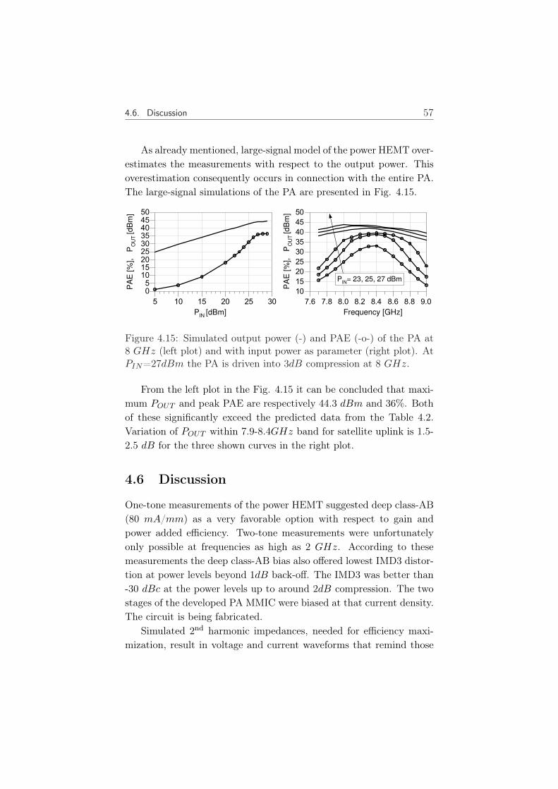
4.6. Discussion 57
As already mentioned, large-signal model of the power HEMT over-estimates the measurements with respect to the output power. Thisoverestimation consequently occurs in connection with the entire PA.The large-signal simulations of the PA are presented in Fig. 4.15.
10 15 20 255 30
51015202530354045
0
50
Pavs [dBm]
PA
E [
%],
Pout
[dB
m]
PA
E [
%],
P
OU
T[d
Bm
]
PIN [dBm]
7.8 8.0 8.2 8.4 8.6 8.87.6 9.0
15
20
25
30
35
40
45
10
50
Frequency [GHz]
PA
E [
%],
P
out
[dB
m]
PA
E [
%],
P
OU
T[d
Bm
]
Frequency [GHz]
PIN
= 23, 25, 27 dBm
Figure 4.15: Simulated output power (-) and PAE (-o-) of the PA at8 GHz (left plot) and with input power as parameter (right plot). AtPIN=27dBm the PA is driven into 3dB compression at 8 GHz.
From the left plot in the Fig. 4.15 it can be concluded that maxi-mum POUT and peak PAE are respectively 44.3 dBm and 36%. Bothof these significantly exceed the predicted data from the Table 4.2.Variation of POUT within 7.9-8.4GHz band for satellite uplink is 1.5-2.5 dB for the three shown curves in the right plot.
4.6 Discussion
One-tone measurements of the power HEMT suggested deep class-AB(80 mA/mm) as a very favorable option with respect to gain andpower added efficiency. Two-tone measurements were unfortunatelyonly possible at frequencies as high as 2 GHz. According to thesemeasurements the deep class-AB bias also offered lowest IMD3 distor-tion at power levels beyond 1dB back-off. The IMD3 was better than-30 dBc at the power levels up to around 2dB compression. The twostages of the developed PA MMIC were biased at that current density.The circuit is being fabricated.
Simulated 2nd harmonic impedances, needed for efficiency maxi-mization, result in voltage and current waveforms that remind those

58 Chapter 4. GaN HEMT X-band Power Amplifier Design
of a parallel-tuned amplifier with shorted harmonics. Realized out-put and interstage matching circuits nearly approximate the optimalharmonic impedances required by the power stage transistors. In 2dB
back-off, the obtained PAE was about 2% below the optimum case.The most undesirable harmonic terminations were those that createdopen circuits seen by the intrinsic device input and output.
Investigation of the transistor model also revealed that feedbackcapacitance CGD, beside CDS , significantly reduces the optimal loadimpedance at the fundamental frequency.
The obtained small-signal insertion gain is 21dB, and it falls by1dB at 7.7 and 8.4 GHz. Hence 1dB gain variation is obtained in thesatellite uplink band 7.9-8.4 GHz. Without accounting for possibleimprovement coming from the harmonic manipulation, peak PAE of31.3% and 42.5 dBm (18 W ) saturated output power can be expectedbased upon device measurements and simulated circuit losses. Theseresults are competitive to the other GaN HEMT two-stage state-of-the-art MMIC results presented in the Fig3.1 [32,33,35,36].

Chapter 5
SiGe and InP based HBTs
As stated in the chapter 3 in connection with the technology inves-tigation, millimeter-wave SiGe HBT and InP HBT technologies of-fer attractively high power densities. The section 3.4 outlined basicproperties of the InP HBT technology from Alcatel-Thales III-V Laband SiGe HBT technology from IHP. Excellent transport propertiesof InP compound and relatively high breakdown field makes the InPHBTs suitable for mm-wave power applications. For instance, mobilityhigher than that in Si, relaxes the trade-off between the base resistanceand ft, which both are dependent on base doping level [53]. Despiteof these advantages, InP HBT based MMICs operating in 68-85 GHz
range, demonstrated lower output powers (up to 80 mW ) than theirSiGe counterparts (up to 125 mW ), as depicted in the Fig.3.3. Ag-gressive scaling of SiGe HBTs reduces the parasitics thereby improvingthe achievable gain demanded by the mm-wave amplifiers. Anotheradvantage of the SiGe HBT technology lies in a thermal conductivityof Si, which is around twice that of InP substrate.
Goal of this chapter is to compare the two types of HBTs in termsof model parameters and a simulated performance. An accurate modelof the ATL’s InP HBT was available as discussed in chapter 3. In thiswork IHP’s SiGe HBT was characterized using a large-signal compactmodel VBIC. First part of this chapter deals with the extraction ofthe model parameters from electrical measurements, and model veri-fication. The modeling part includes the description of the developedmethod for accurate de-embedding of the test structure parasitics from
59
60 Chapter 5. SiGe and InP based HBTs
the small-signal measurements. After that, advantages and limitationsof the SiGe and InP HBTs will be presented, together with the pre-liminary considerations for the InP HBT power amplifier design.
5.1 Modeling of SiGe HBT
Evaluation of power performance of the 0.21 × 0.84µm2 HBT re-quires an accurate large-signal model. One commercial physics-basedmodel of a bipolar transistor is a vertical bipolar inter-company model(VBIC) [173]. SiGe HBTs exhibiting ft of 60GHz [174] and 75GHz
[175] have been accurately characterized using the VBIC, when mea-sured up to 26.5GHz and 50GHz, respectively.
Development of a small-signal equivalent model based on a multi-bias S-parameters of a SiGe HBT is an essential step towards theextraction of VBIC model parameters [174, 176]. Prior to this step,parasitic effects of the RF probe pads and interconnects must be re-moved from the measured S-parameters. A widely used de-embeddingmethod developed by Cho and Burk [177] employs four standard teststructures - two shorts, open and thru - for characterization of the par-asitics surrounding the device. Few standards provide limited infor-mation about the parasitics. This method therefore assumes that thepad and the associated interconnecting line are each representable bya single one-port impedance box. However, as the operation frequencyincreases, this simplified model may cease to be accurate because ofdistributed nature of the interconnects. More advanced methods ac-count for the line distribution in different ways: by separate measure-ment of an on-wafer interconnect assisted by EM-simulation [139], byfitting all lumped-element model parameters to the structure mea-surements [178], or by measuring a number of additional standardstructures [179].
In this work, a simplified variant of the Cho-Burk de-embeddingmethod [180] based on only two standard structures, open and short,was further developed to account for the distribution of the inter-connect admittance. The distribution of the line admittance was es-timated by optimization of one empirical factor. Hereafter, the de-embedded measurement results are applied for a direct parameter ex-

5.1. Modeling of SiGe HBT 61
traction of the small-signal equivalent circuit parameters following theprocedures previously reported in [174] and [181]. Additionally, a de-embedding error resulting from probe positioning inaccuracy will beidentified and corrected. The small-signal model is utilized for param-eter extraction for the large-signal VBIC model based on small-signaland DC measurements. Finally, the VBIC model is experimentallyverified against measurements up to 50 GHz.
5.1.1 De-Embedding of the Test Structure Parasitics
De-embedding of the RF-probe and interconnect line parasitics is pre-requisite for accurate interpretation of the device characteristics. S-parameters provided by IHP were obtained from the 4-finger HBTstructure illustrated in the Fig.5.1. The HBT is connected to theprobe pads by finite-ground coplanar wave-guides (CPWs). The twoCPW lines are to the first order of approximation described by two π-networks on each side of the device as shown in the Fig.5.2. ElementsYpad(11/22) and Yinn(11/22) model the distributed capacitive coupling ofthe interconnect lines and the pads to the ground. The series elementsZpb, Zpc and Ze have predominately inductive behavior. Coupling be-tween the lines due to the gap where the device is situated is modeledthrough Ybc.
Base Collector
Figure 5.1: Central part of the test structure showing four parallelcoupled 0.21× 0.84µm2 HBTs [141].

62 Chapter 5. SiGe and InP based HBTs
Zpb Zpc
Ybc
Zpe
Ypad11 Yinn11 Ypad22Yinn22
Figure 5.2: Equivalent circuit model for the HBT test structure.
Total admittances of the two interconnect lines are calculated fromthe open standard admittance parameters, and used for constructionof the admittance matrix Yline, as
Yline =
[Yopen11 + Yopen21 0
0 Yopen11 + Yopen12
]. (5.1)
In the next step, an empirical factor n is introduced in order todivide the total line admittance, into Ypad and Yinn contributions as
Ypad ' Yline · (n) (5.2)
Yinn ' Yline · (1− n) (5.3)
For n = 1, the total admittance would be associated with the pads,and the equivalent circuit would reduce to the conventional Cho-Burktopology [177]. For 0 < n < 1 it would be distributed. Approxima-tions in the equations (5.2) and (5.3) rely on the fact that the twoseries networks, Zpb-Yinn11 and Zpc-Yinn22, respectively, resonate atmuch higher frequencies than the highest measurement frequency of50 GHz.
Series impedance elements can now be extracted as
Zp = [Yshort − Ypad]−1 (5.4)
Zpe = Zp12 (5.5)
Zpb = (Zp11 − Zp21) · nshift (5.6)
Zpc = (Zp22 − Zp12) /nshift (5.7)

5.1. Modeling of SiGe HBT 63
where Yshort is the admittance matrix of the short-standard measure-ment, and nshift is introduced to correct a de-embedding error result-ing from probe positioning inaccuracy. If the probe reference planesin the HBT structure measurements are shifted as compared to thereference planes in the short-standard measurement, a Zpb and Zpc
impedances would be miss-predicted. A simple way to correct for thisis to multiply Zpb and divide Zpc by a same factor nshift. A proce-dure for estimating nshift from transistor access inductances will beexplained later in this section.
The inductive part of the series element Zpc is plotted vs. frequencyin the Fig.5.3, for two values of the distribution parameter n. Forn=1, the total line admittance to the ground is concentrated in thepad, leading to a frequency dependence of the inductance Lpc. Forn=0.5, the admittance to the ground is distributed along the line. Theresulting Lpc becomes also less dependent on frequency. Frequencydependence of Lpc in the low-frequency range is believed to stem fromuncertainties in the S-parameter measurements. When n=0.5 wasassumed, reduced frequency dependence was correspondingly observedin the extracted small-signal equivalent circuit element values of theinvestigated HBT. Therefore, 0.5 was adopted as an optimum valuefor the de-embedding parameter n.
Lp
c =
im
agZ
pc
/
[pH
]
n=1
n=0.5
10 20 30 400 50
60
65
70
55
75
Frequency [GHz]
Figure 5.3: Extracted inductance of the line connecting the collectorwith the test probe.
The calculated two-port parameters of the equivalent circuit ele-ments are now easily subtracted from the measured multi-bias tran-sistor parameters in following four steps.

64 Chapter 5. SiGe and InP based HBTs
Yd1 = Ymeas − Ypad (5.8)
Yd2 =
Y −1
d1 −[Zpb 00 Zpc
]−1
(5.9)
Yd3 = Yd2 − Yinn −[
Ybc −Ybc
−Ybc Ybc
](5.10)
Zd4 = Y −1d3 − Zpe. (5.11)
Here, Ymeas it the measured admittance matrix of the transistor in-cluding the test structure, and Zd4 is the obtained Z-matrix of thetransistor alone.
5.1.2 Extraction of the Small-Signal Equivalent CircuitParameters
The carefully de-embedded small-signal parameters of the HBT arein following applied for direct parameter extraction for the small-signal equivalent HBT circuit. The applied extraction method relies onsmall-signal S-parameters measured under different bias conditions incut-off, forward active and saturation mode of operation. The small-signal equivalent circuit useful to represent a SiGe HBT biased ina forward active mode was presented in [182] and is reproduced inFig.5.4.
The bias-dependent intrinsic part of the circuit from the Fig.5.4describes the active device in the vertical structure under the emitter.The hybrid-π topology is compatible with the large-signal model ofthe intrinsic transistor in VBIC model. Frequency dependence of thetransconductance gm is controlled by the parameter τ . It accountsfor the excess-phase shift, which becomes noticeable as the frequencyapproaches ft. The Cbc is the depletion capacitance while Cbe containsboth depletion and diffusion components. The intrinsic base resistanceRb is modulated by the mobile carrier concentration in the neutralbase, and by the base width variation due to Early effect.
The extrinsic part of the equivalent circuit from the Fig.5.4 in-cludes the external passive parasitics as well as the parasitic pnp tran-

5.1. Modeling of SiGe HBT 65
sistor, existing between the substrate, base and collector of the HBT.The fixed resistors Rbx, Re and Rcx account for access resistancesbetween the device terminals and the intrinsic device including thecontact resistances. In modern SiGe HBTs significant contribution tothe device capacitances originates from the oxide capacitances. Theseare represented by Cbeo and Cbco. Action of the parasitic pnp devicebiased in cut-off is accounted through the Cbcx, Rs and Ccs elements.
Cbeo
Rbx R
bi
Cbe
Rcx
Rbe
Cbc
Re
Ccs
Rs
Cbcx
Cbco
B C
E E
Extrinsic HBT
Intrinsic HBT
+V
be
-
gm
Vbe
gm0e-j
Figure 5.4: Small-signal equivalent circuit of a SiGe HBT biased inforward active mode.
Fixed Oxide Capacitances
Base-collector and base-emitter oxide capacitances were extracted fromcut-off mode measurements at lower frequencies, where gm0 approacheszero and the access resistors and Rbe can be neglected. Sum of totalB-E and B-C capacitances were estimated from the de-embedded Y-parameters as, respectively,
Cin = = (Y11 + Y12) /ω and Cfb = = (−Y12) /ω. (5.12)
In reverse and slightly forward biased regime, each of the two cal-culated total capacitances can be represented as a sum of a constantoxide capacitance and a bias-dependent depletion capacitance i.e.,
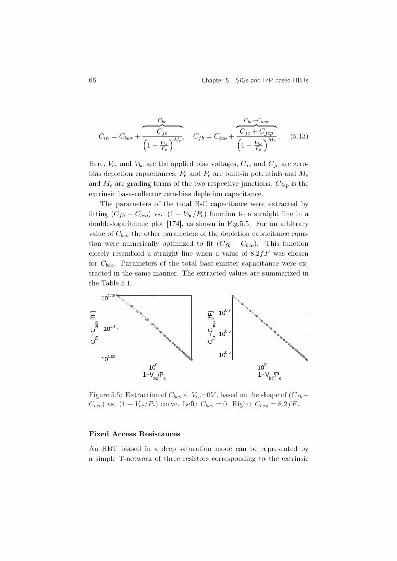
66 Chapter 5. SiGe and InP based HBTs
Cin = Cbeo +
Cbe︷ ︸︸ ︷Cje(
1− VbePe
)Me, Cfb = Cbco +
Cbc+Cbcx︷ ︸︸ ︷Cjc + Cjep(1− Vbc
Pe
)Mc. (5.13)
Here, Vbe and Vbc are the applied bias voltages, Cje and Cjc are zero-bias depletion capacitances, Pe and Pc are built-in potentials and Me
and Mc are grading terms of the two respective junctions. Cjep is theextrinsic base-collector zero-bias depletion capacitance.
The parameters of the total B-C capacitance were extracted byfitting (Cfb − Cbco) vs. (1 − Vbc/Pe) function to a straight line in adouble-logarithmic plot [174], as shown in Fig.5.5. For an arbitraryvalue of Cbco the other parameters of the depletion capacitance equa-tion were numerically optimized to fit (Cfb − Cbco). This functionclosely resembled a straight line when a value of 8.2fF was chosenfor Cbco. Parameters of the total base-emitter capacitance were ex-tracted in the same manner. The extracted values are summarized inthe Table 5.1.
100
100.5
100.6
100.7
1−Vbc
/Pc
Cfb
−C
bco [f
F]
100101.05
101.1
101.15
1−Vbc
/Pc
Cfb
−C
bco [f
F]
Figure 5.5: Extraction of Cbco at Vce=0V , based on the shape of (Cfb−Cbco) vs. (1− Vbc/Pc) curve. Left: Cbco = 0. Right: Cbco = 8.2fF .
Fixed Access Resistances
An HBT biased in a deep saturation mode can be represented bya simple T-network of three resistors corresponding to the extrinsic
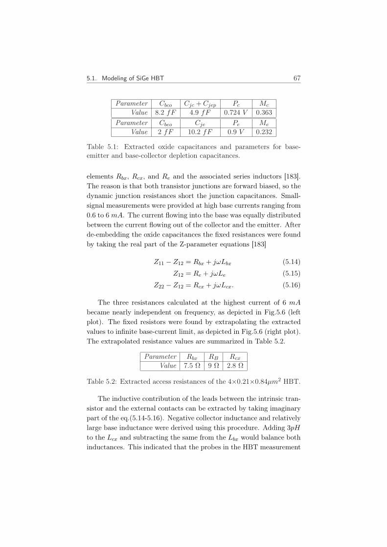
5.1. Modeling of SiGe HBT 67
Parameter Cbco Cjc + Cjep Pc Mc
Value 8.2 fF 4.9 fF 0.724 V 0.363Parameter Cbeo Cje Pe Me
Value 2 fF 10.2 fF 0.9 V 0.232
Table 5.1: Extracted oxide capacitances and parameters for base-emitter and base-collector depletion capacitances.
elements Rbx, Rcx, and Re and the associated series inductors [183].The reason is that both transistor junctions are forward biased, so thedynamic junction resistances short the junction capacitances. Small-signal measurements were provided at high base currents ranging from0.6 to 6 mA. The current flowing into the base was equally distributedbetween the current flowing out of the collector and the emitter. Afterde-embedding the oxide capacitances the fixed resistances were foundby taking the real part of the Z-parameter equations [183]
Z11 − Z12 = Rbx + jωLbx (5.14)
Z12 = Re + jωLe (5.15)
Z22 − Z12 = Rcx + jωLcx. (5.16)
The three resistances calculated at the highest current of 6 mA
became nearly independent on frequency, as depicted in Fig.5.6 (leftplot). The fixed resistors were found by extrapolating the extractedvalues to infinite base-current limit, as depicted in Fig.5.6 (right plot).The extrapolated resistance values are summarized in Table 5.2.
Parameter Rbx RB Rcx
Value 7.5 Ω 9 Ω 2.8 Ω
Table 5.2: Extracted access resistances of the 4×0.21×0.84µm2 HBT.
The inductive contribution of the leads between the intrinsic tran-sistor and the external contacts can be extracted by taking imaginarypart of the eq.(5.14-5.16). Negative collector inductance and relativelylarge base inductance were derived using this procedure. Adding 3pH
to the Lcx and subtracting the same from the Lbx would balance bothinductances. This indicated that the probes in the HBT measurement

68 Chapter 5. SiGe and InP based HBTs
0 10 20 30 40 500
10
20
30
Frequency [GHz]
Re
sis
tan
ce
[]
0 50 100 150 2000
10
20
30
1/Ib [1/A]
Re
sis
tan
ce
[]
Z11-Z12
Z12
Z22-Z12
Z11-Z12
Z12
Z22-Z12
Rcx
Rbx
Rex
Figure 5.6: Extraction of access resistances. Left: Extracted valuesof Z-parameter equations at Ib=6mA. Right: Extrapolation of theaveraged Z-parameters to Ib=∞.
setup could have been shifted around 3µm towards the collector sidecompared to the probe location in the short-standard measurements.The error was compensated by introducing the factor nshift=1.05 ineq.(5.6) and eq.(5.7) in the de-embedding procedure, since the 3pH
inductance corresponds to ∼5% of the inductance of the interconnectsZpb and Zpc in the equivalent circuit of the test structure. After thecompensation, the two access inductances became negligibly small,0.9pH, and were therefore omitted from the equivalent HBT circuit.
Substrate Parasitics
Parasitic coupling to the substrate is modeled through the series con-nected substrate resistance Rs and collector-substrate junction capac-itance Ccs elements in the Fig.5.4. Provided Y-parameters were ob-tained from the HBT biased in cut-off. Collector-substrate voltage wasswept from reverse to a weak forward polarization. Extraction of thesubstrate parasitics is possible after the fixed capacitances and baseand collector resistances have been removed. Neglecting the emitterresistance, the two substrate parasitic elements were estimated fromthe Y-parameters in the low frequency range as proposed in [182],

5.1. Modeling of SiGe HBT 69
Rs ' <(
1Y11 + Y12
), Ccs ' −
=
(1
Y11 + Y12
)−1
. (5.17)
The extracted Ccs was afterwards fitted to the usual depletion capaci-tance expression, as those in eq.(5.13), omitting the oxide capacitanceterm and using the corresponding VBIC parameters, Ms, Ps and Cjcp.The extracted values are listed in the Table 5.3.
Parameter Rs Ms Ps Cjcp
Value 800 Ω 0.14 0.72 V 3.1 fF
Table 5.3: Extracted parameters of the parasitic substrate network.
Hybrid-π Equivalent Circuit
Reverse biased base-emitter junction of the parasitic pnp device con-tributes to the base-collector capacitance through Cbcx element in theequivalent circuit of the Fig.5.4. The elements of the intrinsic devicetogether with Cbcx can be calculated after stepwise de-embedding ofthe previously calculated elements in following order: oxide capac-itances, access resistances in base and collector, substrate-collectorparasitics and finally emitter resistance. The method applied in [180]was used here to extract the remaining elements of the equivalentcircuit. The influence of Cbcx is first removed by manipulating thede-embedded Y-parameters as
Ya = Y11 + Y12 =gbe + jωCbe
1 + Rbi (gbe + jω (Cbe + Cbc))(5.18)
Yb = Y21 − Y12 =gmoe
−jωτ
1 + Rbi (gbe + jω (Cbe + Cbc))(5.19)
Yc = Y22 + Y12 =jωCbcRbi
(gbe + gmoe
−jωτ + jωCbe
)
1 + Rbi (gbe + jω (Cbe + Cbc))(5.20)
where gbe = 1/Rbe is introduced. Using the calculated Ya, Yb and Yc,following useful subfunctions are defined,

70 Chapter 5. SiGe and InP based HBTs
a =1
|Yb|ω→0
=1 + Rbigbe
gmo, (5.21)
b =1ω
√1
|Yb|2− a2 =
Rbi (Cbe + Cbc)gmo
, (5.22)
c = <(
Ya
Ybe−jωτ
)=
gbe
gmo, (5.23)
d = =(
Ya
Ybe−jωτ
)1ω
=Cbe
gmo, (5.24)
τRC = =(
Yc
ω (Ya + Yb)
)= RbiCbc, (5.25)
where the excess phase delay parameter τ is found from
ωτ = − (∠Yb + arctan (ωb/a)) (5.26)
Remaining circuit elements are extracted by solving the eq.(5.21-5.25)as follows
Rbi =b− aτRC
d− cτRC
, (5.27)
gmo =1
a− cRbi, (5.28)
Rbe = cgmo, (5.29)
Cbe = dgmo, (5.30)
Cbc =τRC
Rbi, (5.31)
Cbcx = =(−Y12 − jωCbc
1 + Rbi (gbe + jω (Cbe + Cbc))
)1ω
(5.32)
Some of the calculated element values are plotted vs. frequency inthe Fig.5.7. In general, reasonably low frequency dependence is ob-tained in a wide range of the operating conditions. Above ∼18 GHz,ωτ grows almost linearly with frequency, as expected. Extracted ele-ment values of the hybrid-π equivalent network are summarized in theTable 5.4. It can be seen from the table that the Cbc value is slightly

5.1. Modeling of SiGe HBT 71
higher at Vce=1.5V as compared to the value at 1.0V . This trend isinconsistent with the expected voltage dependence of a depletion ca-pacitance - Cbc should decrease with increasing Vce. However, the sum(Cbc+Cbcx) does decrease with Vce. In fact, it has been found that themodel response is mainly affected by the sum (Cbc+Cbcx), while theaccurate distribution between the intrinsic and extrinsic capacitanceis of less importance.
0 10 20 30 40 500
1
2
3
4
5
Frequency [GHz]
Cbc
[fF]
0 10 20 30 40 500
100
200
300
Frequency [GHz]
Cbe
[fF]
0 10 20 30 40 500
0.1
0.2
0.3
0.4
Frequency [GHz]
ωτ
0 10 20 30 40 500
100
200
300
400
Frequency [GHz]
g m0[m
S]
1mA, 0.5V6mA, 1.0V11mA, 1.5V1mA, 2.0V
Figure 5.7: Frequency dependence of the extracted element values forthe intrinsic device.
Rbi Cbc Cbe Rbe gmo τ Cbcx
Ic/Vce [Ω] [fF ] [fF ] [Ω] [mS] [pS] [fF ]1mA/0.5V 50 3.4 37 2743 29 0.81 2.16mA/1.0V 60 2.9 127 578 165 0.47 1.5
11mA/1.5V 60 3.1 240 280 290 0.26 0.951mA/2.0V 53 2.8 38 2992 31 0.79 0.16
Table 5.4: Extracted element values for the hybrid-π equivalent circuitof the 4× 0.21× 0.84µm2 SiGe HBT at four bias points.
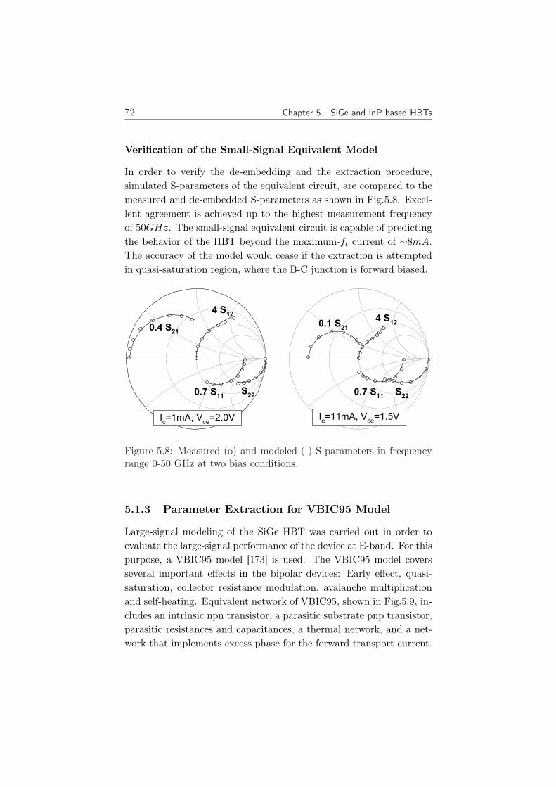
72 Chapter 5. SiGe and InP based HBTs
Verification of the Small-Signal Equivalent Model
In order to verify the de-embedding and the extraction procedure,simulated S-parameters of the equivalent circuit, are compared to themeasured and de-embedded S-parameters as shown in Fig.5.8. Excel-lent agreement is achieved up to the highest measurement frequencyof 50GHz. The small-signal equivalent circuit is capable of predictingthe behavior of the HBT beyond the maximum-ft current of ∼8mA.The accuracy of the model would cease if the extraction is attemptedin quasi-saturation region, where the B-C junction is forward biased.
0.7 S11
0.1 S21
4 S12
S22
0.7 S11
4 S12
S22
0.4 S21
Ic=1mA, V
ce=2.0V I
c=11mA, V
ce=1.5V
Figure 5.8: Measured (o) and modeled (-) S-parameters in frequencyrange 0-50 GHz at two bias conditions.
5.1.3 Parameter Extraction for VBIC95 Model
Large-signal modeling of the SiGe HBT was carried out in order toevaluate the large-signal performance of the device at E-band. For thispurpose, a VBIC95 model [173] is used. The VBIC95 model coversseveral important effects in the bipolar devices: Early effect, quasi-saturation, collector resistance modulation, avalanche multiplicationand self-heating. Equivalent network of VBIC95, shown in Fig.5.9, in-cludes an intrinsic npn transistor, a parasitic substrate pnp transistor,parasitic resistances and capacitances, a thermal network, and a net-work that implements excess phase for the forward transport current.

5.1. Modeling of SiGe HBT 73
Ibcp
Ibep
Iccp
Qbcp
Qbep
Rbip
/qbp
Rbi/q
bR
bx Ibex
Ibc
Ibe
Rci
Rcx
Re
Qbcx
Icc
Qbex
Rs
Qbc
Qbe
Cbco
Cbeo
s
b
c
Parasitic
transistor
Intrinsic
transistor
1OhmQ
cxfItzf
Flxf
Excess-phase
network
Rth
CthI
th
ci
cx
bx b
i
ei
e
Thermal network
Figure 5.9: VBIC95 model equivalent network
Modeling of avalanche multiplication and self-heating was not car-ried out in this work. The parameter extraction described below isbased on pre-knowledge of the thermal resistance Rth = 2200Ω, andweak avalanche parameters AV C1 = 2 and AV C2 = 11.1. Theseparameters were provided in an outdated set of VBIC parameters ofIHP’s 4-finger SiGe HBT having same emitter dimensions.
Some of the extracted values of the small-signal equivalent circuitelements, like fixed capacitances and resistances and parasitic sub-strate resistance, were directly used as parameters for the large-signalVBIC95 model. Parameters for the depletion capacitances were usedas well. The total C-B zero-bias depletion capacitance of 4.9 fF , pre-sented in Table 5.1, was partitioned into the intrinsic Cjc and extrinsicCjep component using the Cbc/Cbcx ratio of 2.5 extracted at peak ft.
Excess-phase parameter τ presented in Table 5.4 ranges between0.8pS at 1mA and 0.26ps at 11mA. Since the excess phase delay inthe VBIC model is independent on the bias, an average value of 0.4 ps
was used for the excess phase delay parameter Td. Such a low valueof the excess phase delay is of minor importance for the small-signalS-parameters well below the cut-off frequency ft.

74 Chapter 5. SiGe and InP based HBTs
Early-Effect Modeling
Modulation of the neutral base width caused by the bias dependentwidth of the depletion regions is called Early-effect. In a common-emitter stage this results in a finite output conductance go. Forwardand reverse Early-voltage parameters Vef and Ver are calculated bysolving two coupled equations [173],
(qfbc − Icc
fbc/gf
o )(1/Vef ) + qfbe(1/Ver) = −1 (5.33)
(qrbe − Iec
rbe/gr
o)(1/Ver) + qrbc(1/Vef ) = −1 (5.34)
where superscripts f and r denote forward and reverse mode of op-eration, respectively, q is the normalized depletion charges and c isthe depletion capacitance normalized to the corresponding zero-biasdepletion capacitance. Junction charge q can be calculated as follows
c =δq
δV=
1(1− V
P
)M=⇒ (5.35)
q =−P
M − 1
(1−
(1− V
P
)(1−M))
(5.36)
where P is the built-in potential, M is the grading coefficient and V
is the applied voltage for the particular junction. Calculated Earlyvoltages for the SiGe HBT became Vef = 83V and Ver = 2.1V .
Diodes and Transport-Current Parameters
Transport current source of the intrinsic device in VBIC is given by[173]
Icc =Is
qb
(exp
(Vbei
NfVt
)− exp
(Vbci
NfVt
)), (5.37)
where Vbei and Vbci are the B-E the B-C voltages, respectively, Vt isthe thermal voltage, Nf and Nr are the forward and the reverse ide-ality factors, respectively, Is is the saturation current and qb is thenormalized base charge. High injection in the base and Early effectare treated by modulation of qb. The high injection effect is modeledthrough forward and reverse knee current parameters, Ikf and Ikr,
5.1. Modeling of SiGe HBT 75
respectively. They acts as a limitation of the exponential current in-crease. After the Early voltages were calculated, the transport currentparameters were extracted in following steps:
• Parameters Is and Nf were extracted from forward Gummelmeasurements up to moderate current level where high-injectionand resistive effects are negligible. Vbc was set to 0V while Vbe
was swept in a range 0.4-0.8 V . Measured Ic versus Vbe, plottedin the logarithmic current plot is almost a straight line, whichslope is proportional to Nf , and which offset on the logarithmicscala is controlled by Is.
• Nr was extracted from the emitter current in the reverse Gum-mel measurements, in which Vbc was swept, and Vce was keptconstant at -0.5 and -1.5V .
• Ikf and Ikr were optimized to fit the collector- and emitter cur-rents to the high-current subrange of the forward and reverseGummel measurement, respectively.
Current of the forward biased base-emitter diode is split into sumof an ideal and a non-ideal component,
Ibe = Ibei
(exp
(Vbei
NeiVt
)− 1
)+ Iben
(exp
(Vbei
NenVt
)− 1
). (5.38)
The ideal and non-ideal diode parameters, Ibei, Nei and Iben, Nen,respectively, can be extracted from the base current in the forwardGummel plot. The non-ideal parameters can be extracted in the lowcurrent range, while the ideal parameters can be extracted from themedium current range where the series resistances of the base andemitter can be neglected. The non-ideal base current turned out to benegligible all way down to 10 pA, which is an indication of a negligiblerecombination currents in the E-B space-charge region [184].
Current through the base-collector diode
Ibc = Ibci
(exp
(Vbci
NciVt
)− 1
)+ Ibcn
(exp
(Vbci
NcnVt
)− 1
). (5.39)

76 Chapter 5. SiGe and InP based HBTs
is also controlled by the ideal, and non-ideal parameters, Ibci, Nci, andIbcn, Ncn, respectively. From measured reverse Gummel plot it is notpossible to distinguish between this current and the current flowingthrough the B-E diode of the parasitic substrate transistor. Bothdiodes are characterized by the same ideality factors in VBIC, butthe parasitic B-E diode has its own saturation currents Ibeip and Ibenp.The ideal and non-ideal saturation currents extracted from the reverseGummel plot were partitioned into B-C and parasitic B-E saturationcurrents using the Cbc/Cbcx ratio of 2.5 extracted at peak ft.
Transport current for the parasitic substrate transistor is given by
Iccp =Isp
qbp
(exp
(Vbep
NfpVt
)− exp
(Vbcp
NfpVt
))(5.40)
where Vbep and Vbcp are voltages across the parasitic B-E and theparasitic B-C diode, respectively. Saturation current Isp and ideal-ity factor Nfp were extracted from the substrate current in forwardGummel plot of the parasitic transistor up to moderate current level,similarly to the intrinsic npn transistor. In this measurement, emitterwas floating, while the substrate-collector voltage was swept keepingVbe at 0.5 V . Normalized parasitic base charge qbp is controlled by theknee current parameter Ikp, which was extracted from the substratecurrent in the high current region.
The base-collector current of the parasitic transistor is modeled as
Ibcp = Ibcip
(exp
(Vbcp
NcipVt
)− 1
)+ Ibcnp
(exp
(Vbcp
NcnpVt
)− 1
)
(5.41)where Ibcip, Ncip and Ibcnp, Ncnp control the ideal and non-ideal currentcomponents, respectively. The parameters were extracted from thereverse Gummel plot of the parasitic transistor, based on the sameprocedure as for the other diodes mentioned above. The extractedDC-parameters are listed in Table 5.5.
Quasi-Saturation Parameters
Quasi-saturation is defined as the region where the intrinsic B-C junc-tion is forward biased, while the external B-C terminal remains reverse

5.1. Modeling of SiGe HBT 77
Param. Value Param. Value Param. ValueIs 2e-18 Nen 2 Nfp 0.996
Nf 1.020 Ibci 1.65e-18 Ikp 0.004Nr 1.015 Ibcn 3.67e-14 Ibcip 3.23e-15Ikf 0.005 Nci 1.057 Ibcnp 1e-25Ikr 0.006 Ncn 2 Ncip 1.01Ibei 6.2e-20 Ibeip 6.62e-19 Ncnp 2Iben 1e-25 Ibenp 1.47e-14Nei 1.032 Isp 2.94e-20
Table 5.5: Extracted parameters for the diodes and transport currents.
biased [185]. In this mode of operation, minority carriers are injectedinto the lightly doped collector, widening the base of the device andthus reducing current gain and storing excess charge in the collector.In a device employing lightly doped collector, the quasi-saturation ismore pronounced due to a high collector resistance. Moreover, collec-tor transit-time tends to be high, reducing the ft [186]. However, lowcollector doping level has a beneficial impact on break-down voltageand fmax due to decreased electric field and capacitance of the B-Cjunction, respectively [186,187].
Parameters responsible for the device behavior in quasi-saturationare Rci, γ, Vo, Hrcf , Qco, which detailed explanation can be found in[188]. The Qco is a zero-bias collector charge affecting high-frequencymodeling and will be treated in the next section. The first four pa-rameters are optimized by fitting the output characteristics in quasi-saturation and saturation region. The optimization result is shown inFig.5.10. The extracted parameter values are presented in Table 5.6.The Rci is resistance of the intrinsic collector. Increasing the Rci from18 to 30Ω in the optimization would have yielded almost perfect fit inthe quasi-saturation part of the characteristic. This resistance is how-ever almost double of what was expected from the layer properties ofthe device structure. This deviation of the Rci from the physics basedexpectations will also be discussed in the next subsection in connectionwith transit-time modeling.
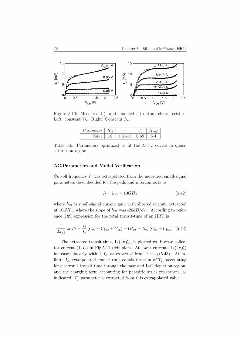
78 Chapter 5. SiGe and InP based HBTs
0.9 V
0 0.5 1 1.5 2 2.50
5
10
15
Vce [V]
I c [
mA
]
0.85 V
0.95 V
Vbe
=1 V
0 0.5 1 1.5 2 2.50
5
10
15
Vce [V]
I c [
mA
]
Ib=1e-3 A
1e-9 A
12.5e-6 A
25e-6 A
50e-6 A
Figure 5.10: Measured (.) and modeled (-) output characteristics.Left: constant Vbe. Right: Constant Ibe.
Parameter Rci γ Vo Hrcf
Value 18 1.3e-13 0.68 5.4
Table 5.6: Parameters optimized to fit the Ic-Vce curves in quasi-saturation region.
AC-Parameters and Model Verification
Cut-off frequency ft was extrapolated from the measured small-signalparameters de-embedded for the pads and interconnects as
ft = h21 × 10GHz (5.42)
where h21 is small-signal current gain with shorted output, extractedat 10GHz, where the slope of h21 was -20dB/dec. According to refer-ence [189] expression for the total transit-time of an HBT is
12πft
' Tf +Vt
Ic(Cbc + Cbcx + Cbe) + (Rcx + Re) (Cbc + Cbcx) (5.43)
The extracted transit time, 1/(2πft), is plotted vs. inverse collec-tor current (1/Ic) in Fig.5.11 (left plot). At lower currents 1/(2πft)increases linearly with 1/Ic, as expected from the eq.(5.43). At in-finite Ic, extrapolated transit time equals the sum of Tf , accountingfor electron’s transit time through the base and B-C depletion region,and the charging term accounting for parasitic series resistances, asindicated. Tf parameter is extracted from this extrapolated value.

5.1. Modeling of SiGe HBT 79
0.01 0.1 1 10 200
20
40
60
80
100
120
140
160
180
200
Ic [mA]
f t [
GH
z]
V =0.5V, meas.
V =0.5V, VBIC
V =1.0V, meas.
V =1.0V, VBIC
V =2.0V, meas.
V =2.0V, VBIC
0 1 2 30
0.5
1
1.5
2
2.5
3
3.5
1/Ic [1/mA]
1 /
( 2
ft )
[p
S]
Vce = 1 V
Vce = 1.5 V
T +(R +R ) CF ci cx bc
ce
ce
ce
ce
ce
ce
Figure 5.11: Left: Transit time extrapolated at 10GHz vs. inversecollector current. Right: Measured and modeled cut-off frequency ft
The total transit time in the VBIC model is bias dependent throughparameters Xtf , Itf , Vtf and Qtf . These parameters were optimized tofit the ft-Ic plots in the high-current end. Results of the optimizationare shown in Fig.5.11 (right plot). The quasi-saturation parameterQco was included in the optimization of the 0.5V -curve, since at highercurrents and 0.5V the device approaches quasi-saturation region.
As in the case of the DC output characteristics, it was not pos-sible to accurately capture ft in quasi-saturation using Rci = 18 Ω.By increasing the Rci to 30 Ω, remarkably better fit was possible.Non-physical behavior of VBIC in quasi-saturation has also been rec-ognized by de Graaff [190]. The discrepancy between the measuredand modeled DC output characteristics and ft in quasi-saturation re-gion will possibly lead to a slight overestimation of the output powerand efficiency performance of the HBT.
Parameter Rbi controlling the intrinsic base resistance was opti-mized to fit the measured S11 and S21 parameters over a range ofcollector currents. The extracted AC-parameters are summarized inTable 5.7. Comparison between measured and modeled S-parametersis presented in the Fig.5.12. Good agreement was achieved up to 50GHz, and beyond maximum-ft current of 8mA.

80 Chapter 5. SiGe and InP based HBTs
Parameter Value Parameter Value Parameter ValueTf 5.9e-12 Vtf 0.35 Rbi 145
Xtf 30 Qtf 1e-9Itf 0.8 Qco 6e-15
Table 5.7: Extracted VBIC AC-parameters.
0.7 S11
0.1 S21 4 S
12
S22
0.7 S11
0.4 S21 4 S
12
S22
Ic=1mA, V
ce=2.0V I
c=11mA, V
ce=1.5V
Figure 5.12: S-parameters for the 4×(0.21×0.84µm2) SiGe HBT, mea-sured (o) and simulated using VBIC (-) in frequency range 0-50 GHzat two bias conditions.
Apart from the slight discrepancy in the quasi-saturation, goodconsistency between measured and modeled data was achieved in 0-50GHz range. Not shown are the simulated Gummel-plots as well theDC-plots of the parasitic substrate transistor, which agreed with themeasured DC-data as well. In following section the VBIC model willbe used to estimate the power and gain performance of the SiGe HBTat 73.5 GHz.
5.2 SiGe HBT and InP HBT Performance atE-band
The rest of this chapter will explore the possibilities of the SiGe HBTand InP HBT to act as E-band power amplifiers. The equivalent cir-cuit parameters will provide a valuable link between the device physics

5.2. SiGe HBT and InP HBT Performance at E-band 81
and performance. Limitations arising from the two technologies willbe discussed. Preliminary considerations for the design of InP HBTpower amplifier will also be presented.
5.2.1 Device Parameters
The 1.5×10µm2 InP HBT exhibits peak in the maximum oscillationfrequency fmax when biased at IC=24mA, VCE=1.6V . The peak fmax
for the 4×0.21×0.84µm2 SiGe HBT occurs at around three times lowercurrent and same voltage. Output power for a class-A biased device isideally given by 0.5ICEVCE . Therefore, three parallel-connected SiGeHBTs, biased at peak fmax, would ideally be capable to produce samepower as the single InP HBT. The resulting SiGe HBT configurationcould in principle be realized as a single 12-finger transistor or as twocombined 6-finger units. Important parameters for the two devices arecompared in the Table 5.8. The parameters for the SiGe HBT are cal-culated by simple 3× scaling of the extracted VBIC model, neglectingthe possible unwanted effects like combining losses and mutual heatingbetween the adjacent transistors.
The superior thermal conductivity od Si as compared to InP sub-strate counts towards the relatively low thermal resistance Rth of thetotal SiGe HBT device as indicated in the table. Hence the SiGedevice will develop lower junction temperature than InP HBT, whensimilar bias is applied to the devices.
It can be concluded from the Table 5.8 that InP HBT exhibits peakin fmax at about 7.5 times lower current density Jbias as compared toSiGe device. Larger zero-bias depletion capacitances Cje and Cjc ofthe InP HBT device offsets the advantage of lower transit time TF ,since the two devices operate at almost same Ibias (recall the equation3.5). As a result, the two devices exhibit comparable ft.
5.2.2 HBTs in Power-Amplifiers
Simulated load trajectories of the two common-emitter connected de-vices biased at 1.6 V and driven in 1dB gain compression are depictedin the Fig.5.13 (left and middle plot, respectively). The trajectoriesare overlayed on the constant-Vbe output characteristics. Investigated

82 Chapter 5. SiGe and InP based HBTs
SiGe InP Unit RemarksHBT HBT
AE 2.1 15 µm2 Emitter areaIbias 24 23 mA
Jbias 11.4 1.53 mA/µm2
ft 170 200 GHz
fmax 170 200 GHz
Rth 733 1250 K/W
Cje 30.4 42 fF
Cjc 14.7 32 fF intrinsic + extrinsicCbeo 6 0 fF
Cbco 25 0 fF
Rci 6 6 ΩRcx 0.9 9.4 ΩVoff <0.03 0.18 V C-E offset voltage
BVCEO 1.9 >7 V
TF 0.59 0.4 ps transit time through baseand B-C depletion region
Table 5.8: Parameters of the 3× scaled (4×0.21×0.84µm2) SiGe HBTand (1.5×10µm2) InP HBT when biased for peak fmax occurring atVCE=1.6V . Unless stated otherwise, the parameter names have theirusual meaning as defined in the VBIC model.
operating points and PA performance are summarized in Table 5.9.Optimum load impedances ZOPT for maximum power output wereselected based on load-pull simulations.
The SiGe HBT was biased at peak-fmax bias point (1.6V /24mA)which incidentally also is a near class-A bias point for that device.When the bias voltage was increased to 1.9V , the output referred1dB-compression power P1dB increased from 8.9 to 10.1 dBm, 3dB-compression power P3dB increased to 13.3dBm. This also pushed theload cycle further beyond the break-down voltage BVCEO of 1.9 V .It has been demonstrated however that the SiGe devices can toleratesuch operating conditions if the bias circuit presents a low enoughresistance to the transistor’s base [85, 191].

5.2. SiGe HBT and InP HBT Performance at E-band 83
Vce [V] Vce [V]
Ic [m
A]
Vce [V]
Ic [m
A]
SOA
Break-downregion
I c [
mA
]
I c [
mA
]
I c [
mA
]
1.0 2.0 3.0 4.0 5.00.0
InP HBT:
VCE
=2.4 V, IC
=20 mA
InP HBT:
VCE
=1.6 V, IC
=19 mA
SiGe HBT:
VCE
=1.6 V, IC
=24 mA
10
20
30
40
50
0
60
10
20
30
40
50
0
60
10
20
30
40
50
0
60
1.0 2.0 3.0 4.0 5.00.0 1.0 2.0 3.0 4.0 5.00.0
Vce
[V] Vce
[V] Vce
[V]
Figure 5.13: Load cycles simulated using Harmonic Balance in ADSat 73.5 GHz. Left: 3× (4×0.21×0.84µm2) SiGe HBT. Middle andright: 1.5×10µm2 InP HBT at two different operating points.
If biased for maximum fmax, the InP HBT would operate nearsaturation which would cause premature gain compression. Class-Abias is therefore provided by reducing the current from 23 to 19mA forthat transistor as indicated in the Fig.5.13 (middle plot). As a result,the small-signal transducer gain Gt dropped from 6.75 to 6.3 dB. Highcollector resistance Rcx and C-E offset voltage Voff of the InP HBTpresented in the Table 5.8 impedes the load trajectory to enter thelow-voltage part of the output characteristics. When biased at 1.6V ,the InP HBT generated 2.5dB lower P1dB than the SiGe HBT, as canbe concluded from data in the Table 5.9.
InP HBT exhibited larger voltage swing when VCE was increased to2.4V as depicted in the Fig.5.13 (right plot). This resulted in superiorP1dB and power-added efficiency of that device. This bias point is stilldeep inside the safe operating area (SOA), and far below the BVCEO
of 7V . The indicated break-down points provided by ATL have beenobtained by imposing a constant base current [192].
In a bipolar device positive feedback exists between the currentand the junction temperature [193]. This self-heating effect causes theslopes of the constant Vbe curves in the Fig.5.13 to increase with thecollector current and the collector voltage, that is, with the dissipatedDC-power. The most severe effect of that mechanism is a thermal-runaway which can destroy the device. The DC characteristics in theFig.5.13 (middle plot) indicate that safe operation of InP HBT would

84 Chapter 5. SiGe and InP based HBTs
SiGe HBT InP HBT UnitICE/VCE 1.6V /24mA 1.6V /19mA 2.4V /20mA
Gt 5.9 6.3 6.3 dB
Zin 7.7-j6.1 15-j2 15-j1 ΩZOPT 19+j22 41+j21 49+j30 ΩP1dB 8.9 6.4 11.4 dBm
P3dB 12 9.4 13.4 dBm
PAE1dB 13 9.6 18 %PAE3dB 18 14 23 %
Tmax 56 64 86 C
Table 5.9: Summary of performance for the three amplifiers from theFig.5.13.
not be possible by imposing constant Vbe at 2.4V/20mA. Imposing aconstant base current, however, would make the slope of the collectorcurrent almost independent on the dissipated power. This can be seenin the Ic-Vce characteristics shown before in the Fig.3.11. Very largeresistor in series with the base supply voltage would have the sameeffect. According to the simulations, a 320-Ω resistor would be suffi-ciently high. Such bias topology has been chosen for the 2.4V biasing.The resulting output characteristics are indicated in the Fig.5.13 (rightplot). Base supply voltage was swept from 0.78 to 1.02V to obtain theshown curves. Operating point 2.4V/20mA was selected for the poweramplifier development, described later in chapter 6. Eight devices candeliver total P1dB of 20.4dBm.
Device temperature under large signal excitation is calculated as
T = Tamb + Rth (Pdc + Pin − Pout) (5.44)
where Tamb is the ambient temperature of 27C, Pdc is the consumedDC-power, Pin is the generator power delivered to the device at thefundamental frequency, and Pout is a sum of powers delivered by theamplifier at fundamental and harmonic frequencies. Maximum tem-peratures Tmax presented in the Table 5.9 were developed with nodrive signal applied to the HBTs. Temperature dropped with increas-ing drive power. Above 2-3 dB compression level, it rose again, since

5.3. Discussion 85
the gain (Pout-Pin) dropped rapidly. The SiGe HBT amplifier exhib-ited lowest temperature due to the lowest Rth. The 2.4V InP HBTdeveloped highest temperature due to the relatively large Rth andPdc. The temperature increase due to the thermal coupling betweenthe three 4-finger SiGe transistors was neglected.
As argued before, high collector resistance Rcx is an importantdisadvantage of the InP HBT under investigation. To show this, theRcx was reduced from 9.4Ω to a value of 0.9Ω present in the SiGeHBT. Without re-optimization of the ZOPT , P1dB delivered by theInP HBT (2.4V bias) increased by 1.4dB.
Another obvious difference between the SiGe HBT and InP HBTamplifier data listed in the Table 5.9 is their input impedance Zin
and load impedance ZOPT . The impedances are much lower for theSiGe device. This would have negative impact on the bandwidthand combining losses in amplifier stages combining many devices.Large oxide capacitance Cbco = 25fF (see Table 5.8) existing be-tween the base and collector of the SiGe HBT significantly lowersthe impedance levels of the SiGe device. With Cbco set to zero, asin the InP HBT, the SiGe amplifier would show substantially higherimpedances, ZOPT=39.5 + j26 and Zin=16− j8.
The quality factors Q (ratios between the imaginary and real parts)of the two impedances ZOPT and Zin also remarkably dropped whenthe Cbco was removed. A high Q of an impedance to be matched limitsthe achievable bandwidth as mentioned in section 4.3. It is worth tonote that the gate-drain capacitance had similar effect regarding theload Q of the GaN HEMT amplifier, discussed in the section 4.3.
5.3 Discussion
This chapter explored applicability of two modern millimeter-waveHBTs for signal power generation in the middle of the E-band fre-quency range 71-76 GHz. For this purpose a large-signal VBIC modelwas utilized to characterize the 4-finger SiGe HBT from IHP foundry.
A simple technique has been suggested to account for distributednature of transistor test structure. The method can be easily usedto improve the accuracy of the conventional open-short de-embedding

86 Chapter 5. SiGe and InP based HBTs
techniques. A procedure for identifying and correcting a de-embeddingerror resulting from probe positioning inaccuracy was also suggestedand applied in direct parameter extraction of the small-signal equiva-lent circuit elements. The subsequent extraction of the VBIC modelparameters resulted in good agreement with the DC measurementsand the small-signal measurements under various bias conditions, andslight discrepancy in quasi-saturation.
For operation at peak fmax, the SiGe HBT must draw around7.5 times higher current per unit emitter area compared to the InPdevice. Three parallel connected 4-finger SiGe HBTs (or a single 12-finger device) draw same current as the single-finger InP HBT. If thetemperature rise due to the thermal coupling within the three SiGetransistors was disregarded, the SiGe HBT would have developed lowertemperature compared to the InP HBT, despite of much higher currentdensity. This is primarily due to the excellent thermal managementand to some extent due to relatively low bias voltage of the silicondevice. Hence, the main advantage of the SiGe HBT is the good heatdissipation that enables high current density, while InP HBTs benefitfrom high breakdown voltage.
The SiGe transistor also showed much lower input and load impe-dances than the InP transistor. This is in part a consequence of highB-C oxide capacitance of the SiGe device. High breakdown voltageof the InP HBT opens the possibility to obtain higher power andefficiency and to further enhance the load impedance, compared tothe 12-finger SiGe transistor. This advantage, concerning the powerand efficiency, is severely diminished by high resistance appearing inthe collector of the InP transistor.
Eight InP HBTs having total emitter area 8×(1.5×10µm2) arecapable of generating more than 100 mW E-band power under 1dB
compression, while drawing 160 mA from a 2.4V supply.

Chapter 6
InP HBT E-band PowerAmplifier Design
This chapter concentrates on design of indium-phosphide HBT basedpower amplifier MMIC for potential application in E-band communi-cation systems operating in the frequency range 71-76 GHz. Introduc-tory considerations concerning the capabilities of a single 10×1.5 µm2
HBT connected in common-emitter (CE) configuration, have been out-lined in section 5.2. Here the maximum power gain and the stabilityfactor of the CE stage will be compared to those of the common-base(CB) and the cascode stages. The CE configuration was selected forthe power amplifier design as the only solution exhibiting uncondi-tional in-band stability.
Multi-finger devices are normally used for high-frequency InP HBTpower amplifier designs. Such unit-transistor cells were not availablein the used process. The four-transistor power cell containing fourcombined single-finger 10×1.5 µm2 HBTs was therefore developed.Equal combining characteristics and equal loading of each HBT areimportant prerequisites for optimal utilization of a power cell [194].Like all the other networks of the amplifier chip, the power cell pas-sive structure was simulated using ADS electromagnetic simulationprogram, Momentum. Circuit simulations of the power cell with em-bedded HBTs will reveal uniform combining characteristics and HBTloading.
87

88 Chapter 6. InP HBT E-band Power Amplifier Design
The common-emitter connected HBTs designed for mm-wave ap-plications have tendency to oscillate at lower frequencies where theirpower gain is higher. The parasitic oscillations can cause distortion bymodulating the desired signals. Great care was put on the stabiliza-tion of the amplifier. This chapter will describe simulation methodsapplied for detection of even-mode oscillations as well as their elimi-nation by use of resistors in the bias circuitry. A suggested simulationmethod applied to predict and eliminate odd-mode oscillations in thePA chip will be presented as well.
This chapter will furthermore describe the operation and perfor-mance of the developed power MMIC. Input/output return loss andgain of the amplifier chip were measured under small-signal drive. Theexperimental setup will be outlined and the measured data will be pre-sented along with the simulated ones. The simulated power and poweradded efficiency will represent record performance levels for an InPHBT power amplifier operating above 50GHz. This InP HBT poweramplifier is a first two-stage solution demonstrated in that technologyin the 50-140GHz range.
6.1 Transistor Configuration
Millimeter wave HBT power amplifiers are mostly implemented incommon-base (or grounded-base) [70, 73, 195] and cascode transistorconfigurations [83,96,195]. These configurations are suitable for mm-wave power amplifiers, because they provide higher gain as comparedto common-emitter and common-collector HBTs. Single-stage InPHBT amplifiers have demonstrated 3.5 dB gain at 255 GHz in CEtopology [196] and 7 dB gain at 176 GHz in CB topology [70]. Un-like the common-emitter amplifiers, the CB amplifiers are operatedin a potentially unstable frequency region. Circuit stability requirestherefore special attention in the CB designs. In the potentially un-stable frequency range, maximum stable gain (MSG) is a figure ofmerit of an HBT. The common base MSG can be significantly loweredby the effect of layout parasitics including base access inductance andcollector-emitter external capacitances [70, 73, 197]. If not accurately

6.1. Transistor Configuration 89
modeled, these parasitics can also introduce uncertainty in the stabil-ity analysis of the CB amplifiers [70, 73]. This problem is, however,not so severe in CE amplifiers. Inductance in series with the emittercan actually deteriorate the gain of the CE connected device. Thisproblem is however naturally solved by direct connection of the emit-ter to the coplanar ground planes. Connection of the emitter to thelarge metal planes will also improve removing the heat generated inthe HBT, as it will be discussed in the next section.
A cascode is a two-transistor configuration composed of a common-emitter stage followed by a common-base stage. It requires less chiparea per unit gain, as compared to CB and CE topologies. A cas-code is, moreover, considered to have better thermal stability as com-pared to the single-transistor topologies [96,198]. Cascode gain can beseverely reduced by a parasitic inductance of the decoupling capacitorin the base of the CB stage [96]. As in the case of CB amplifiers,the stability of the cascode cell is one of the essential design issues.Resistive terminations at the input/output of the mm-wave HBTs arecommonly required to avoid the parasitic oscillations [83, 96,199].
Basic gain and stability properties of the used InP HBT connectedin CE, CB and cascode configurations were investigated using ADSsimulator and the HBT model presented in the section 3.4.1. Thethree simulated configurations including biasing details are shown inthe Fig.6.1. With the aim of comparison the HBTs were biased at sameoperating conditions, 20 mA collector current and 2.4 V collector-emitter voltage. The resistor Rstab serves to stabilize CB and Cascodestages. In following, performance of the three HBT configurations willbe compared before and after insertion of Rstab.
An unconditionally stable amplifier stage has a Rollet’s stabilityfactor K larger than unity, and a positive stability measure [172]. IfRstab was not inserted in CB and Cascode, only the CE stage be-haved unconditionally stable, with K'2, in the frequency band ofinterest 71-76 GHz, as shown in Fig.6.2. The CB HBT appears tobe potentially unstable in practically whole frequency range up to 150GHz. The gain and stability factor calculated in ADS at the centerfrequency 73.5 GHz are collected in the Table 6.1. The stability mea-sure (not shown) was positive for all amplifiers after Rstab was inserted

90 Chapter 6. InP HBT E-band Power Amplifier Design
2.4 V 1.6 V
3.2 V
4.8 V
Rstab
160
Ohm
20 mA20 mA
22
Ohm
20 mA
Common-emitter (CE) Common-base (CB) Cascode
Rstab
-0.8 V
2.4 V
Figure 6.1: Simulation setups for the investigated transistor configu-rations including biasing and stabilizing details.
in CB and Cascode. Since the CE stage was unconditionally stable,its power gain is given as a maximum available gain (MAG) [172]. Itcan be concluded from the table that the common-emitter MAG issubstantially lower as compared to MSG of the CB and the cascodeconnected HBTs, before Rstab was inserted.
1 10 100 200
0
1
2
-1
3
Sta
bili
ty f
acto
r(K
)
Frequency [GHz]
CE
CB
Cascode
Figure 6.2: Simulated K-factor for the investigated transistor config-urations from the Fig.6.1, without Rstab inserted.
To obtain the same level of stability (K=2 at 73.5 GHz) the re-sistors were inserted at the input of the CB and the cascode HBT asshown in the Fig.6.1. As a result, power gain of the CB stage reducedto 4.1 dB, which is more than 2 dB below the gain of the CE stage.The power gain of the cascode amplifier also reduced substantially, to15.9 dB. However, the cascode gain remained superior.
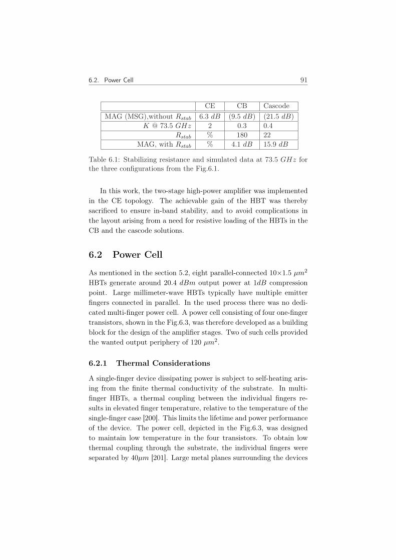
6.2. Power Cell 91
CE CB CascodeMAG (MSG),without Rstab 6.3 dB (9.5 dB) (21.5 dB)
K @ 73.5 GHz 2 0.3 0.4Rstab % 180 22
MAG, with Rstab % 4.1 dB 15.9 dB
Table 6.1: Stabilizing resistance and simulated data at 73.5 GHz forthe three configurations from the Fig.6.1.
In this work, the two-stage high-power amplifier was implementedin the CE topology. The achievable gain of the HBT was therebysacrificed to ensure in-band stability, and to avoid complications inthe layout arising from a need for resistive loading of the HBTs in theCB and the cascode solutions.
6.2 Power Cell
As mentioned in the section 5.2, eight parallel-connected 10×1.5 µm2
HBTs generate around 20.4 dBm output power at 1dB compressionpoint. Large millimeter-wave HBTs typically have multiple emitterfingers connected in parallel. In the used process there was no dedi-cated multi-finger power cell. A power cell consisting of four one-fingertransistors, shown in the Fig.6.3, was therefore developed as a buildingblock for the design of the amplifier stages. Two of such cells providedthe wanted output periphery of 120 µm2.
6.2.1 Thermal Considerations
A single-finger device dissipating power is subject to self-heating aris-ing from the finite thermal conductivity of the substrate. In multi-finger HBTs, a thermal coupling between the individual fingers re-sults in elevated finger temperature, relative to the temperature of thesingle-finger case [200]. This limits the lifetime and power performanceof the device. The power cell, depicted in the Fig.6.3, was designedto maintain low temperature in the four transistors. To obtain lowthermal coupling through the substrate, the individual fingers wereseparated by 40µm [201]. Large metal planes surrounding the devices

92 Chapter 6. InP HBT E-band Power Amplifier Design
230 m
Transistor
B E C
outputinput MIM
Figure 6.3: Layout of the power cell containing four 10×1.5 µm2 HBTs.
act as heat spreaders. The heat spreaders decrease the device tem-perature by transporting the heat from the emitter posts to the coolregions of the substrate. This technique can significantly improve theself-heating characteristics of the device [201, 202]. Central devices ofa multi-finger cell can be expected to be mostly affected by the ther-mal coupling [200]. The two central ground planes help removing thetemperature from the two central devices.
6.2.2 High-frequency Behavior of the Power Cell
Behavior of the passive structures of the power cell was analyzed usingMomentum electromagnetic simulator. The calculated 14-port matrixwas then imported in Agilent ADS for circuit simulations. To facil-itate the construction of the power amplifier matching circuits, thepower cells are pre-matched at the input by use of ∼0.3pF MIM ca-pacitors, as indicated in the Fig.6.3. The four emitters are connectedto the top metal plate by vias, located on both sides of the transis-tors. This eliminates undesired inductance in series with the emitters,therefore preventing gain degradation. The two central ground-planes,

6.2. Power Cell 93
connected by the air-bridges to the outer ground planes provide addi-tional grounding for the two innermost transistors. This prevents thatthe top metal acts as a common lead for all the emitters.
In a well behaved power cell all transistors should operate equally.This implies equal combining characteristics and equal load impedancefor each transistor [194]. The combining characteristics of the powercell were first verified in ADS simulator by comparing S-parameters oftwo different arrangements. In the first arrangement, only two outertransistors were connected in the passive power cell multi-port. Inthe second arrangement, only two inner transistors were connected.The results of the two simulations are plotted in the Fig.6.4. The cellbehaves practically the same regardless of the transistor group used,and well beyond the E-band frequency range 71-76 GHz.
60 8040 100
0.3
0.4
0.5
0.2
0.6
-80
-60
-40
-20
-100
phase(S
22) [d
eg]
0
Frequency [GHz]
mag(S
22)
60 8040 100
-80
0.08
0.10
0.12
0.14
0.06
0.16
Frequency [GHz]
mag(S
12)
60 8040 100
0.30
0.35
mag(S
11)
0.25
0.40
-150
-170
-130
Frequency [GHz]
phase(S
11) [d
eg]
60 8040 100
-140
-160
-120 phase(S
21) [d
eg]
3.0
1.0
2.5
2.0
1.5
20 phase(S
12) [d
eg]
0
-20
-40
-60
mag(S
21)
Frequency [GHz]
Figure 6.4: Comparison of the simulated S-parameters for the twoarrangements in which only the two outer HBTs (-o-) and only thetwo inner HBTs (-) were connected to the power cell passive structure.
Another simulation was performed to verify the load impedancepresented to the transistors. Here all four transistors were embeddedin the cell multi-port. The cell was terminated by (8.5+j8) Ω, aiming

94 Chapter 6. InP HBT E-band Power Amplifier Design
to provide the optimum load impedance (49+j30) Ω to each transis-tor, which will enable the transistors to deliver a high output power,as mentioned in the section 5.2. At the input, the cell was driven bya voltage generator having impedance (10.9+j0.7) Ω providing mini-mum input reflection. The impedance seen by the outer and the innertransistor outputs became, (47.5+j29.5) Ω and (51+j31) Ω, respec-tively, which is very near the optimum impedance. In fact, the twoobtained load impedances lie inside a 0.05dB load-pull contour simu-lated and plotted on Smith-chart.
In reference [194], uniformity of an X-band FET power cell hasbeen improved by employing asymmetric combiner layouts. The asym-metry has been introduced in form of slits and by adjusting the linewidths [194]. In this work no such adjustments were necessary. Theresults presented in this section suggest an equal transistor operationin the developed power cell.
6.3 Amplifier Circuit
As depicted in the Fig.6.5 the amplifier is based on a driver stageand a high-power stage. Each stage was constructed using the twopre-matched 4-transistor power cells. The input of the driver stagewas matched using small-signal impedance levels for minimum small-signal reflection. On contrary, the output of that stage was matchedfor high power output, to avoid premature power-gain compression inthat stage.
50-generator
4x10 m
50-load
VBB2
VCC
VBB1
VCC
Output
match
/
combiner
Interstage
matching
4x10 m
Input
match
/
combiner
4x10 m
Interstage
matching
4x10 m
VBB2
VCC
VBB1
VCC
Figure 6.5: Block-diagram of the developed power amplifier.

6.3. Amplifier Circuit 95
When selecting the driver stage periphery, engineering trade-off ex-ists between the power added efficiency and the driver’s output powercapability, as discussed in section 4.4 dedicated to the GaN HEMTamplifier design. In this amplifier, the ratio between the two periph-eries, 1/1, is much higher as compared to the periphery ratio of theGaN HEMT amplifier, which is 1/2.7. Such large driver periphery isrequired because of the relatively low gain of the mm-wave HBT, whichis 6.3 dB at 73.5 GHz. The periphery ratio of 1/1 provides a drivercircuit saturating at high power levels, improving linear operation asrequired in communication systems. According to the ADS simula-tions of the amplifier circuit, the driver-stage HBTs are backed-off by3.6 dB, when the power stage is in 1dB compression.
An apparent advantage of having two separate power cells in thedriver stage is the combiner-less interstage matching circuit. Absenceof an additional combiner reduces losses between the two stages, thusrelaxing the demand for high-power capability of the driver stage. Asillustrated in the Fig.6.6, the signal is split at the input of the driverstage instead, where the power dissipation is of no importance for thedriver stage linearity.
The coplanar waveguides in the impedance matching circuits areillustrated using the thick lines in the circuit diagram in Fig.6.6. Com-plete schematic and component values can be found in Appendix B.Like the HBT power cells, all the networks were electromagneticallysimulated using Momentum software.
Series coupling capacitors Cs1, Cs2 and Cs3 isolates the DC-biasof the two stages from each other as well as from the external 50Ωequipment. At the same time, the three MIM capacitors serve forimpedance transformation in the matching networks. On the otherhand, quarter-wavelength stubs, shorted at one end, act as nearlyopen circuits. Numerous air-bridges (not shown in the schematic),connecting the ground planes along all the CPW lines, and across thejunctions and bends, were used to suppress slot-line mode excitation[203]. The parasitic effects of the air-bridges have significant influenceon the impedance transformation in the matching networks.
The "Bias and stabilizing" boxes in the circuit diagram of theFig.6.6 contain passive networks for AC/DC decoupling and even-
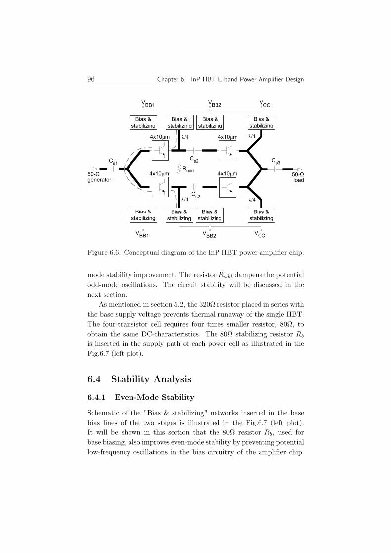
96 Chapter 6. InP HBT E-band Power Amplifier Design
Cs3C
s1
Rodd
Cs2
VBB2 V
CC
4x10 m4x10 m
VBB1
50-generator
Cs2
4x10 m4x10 m 50-load
/4 /4
/4 /4
VBB2
VCC
VBB1
Bias &
stabilizing
Bias &
stabilizing
Bias &
stabilizing
Bias &
stabilizing
Bias &
stabilizing
Bias &
stabilizing
Bias &
stabilizing
Bias &
stabilizing
Figure 6.6: Conceptual diagram of the InP HBT power amplifier chip.
mode stability improvement. The resistor Rodd dampens the potentialodd-mode oscillations. The circuit stability will be discussed in thenext section.
As mentioned in section 5.2, the 320Ω resistor placed in series withthe base supply voltage prevents thermal runaway of the single HBT.The four-transistor cell requires four times smaller resistor, 80Ω, toobtain the same DC-characteristics. The 80Ω stabilizing resistor Rb
is inserted in the supply path of each power cell as illustrated in theFig.6.7 (left plot).
6.4 Stability Analysis
6.4.1 Even-Mode Stability
Schematic of the "Bias & stabilizing" networks inserted in the basebias lines of the two stages is illustrated in the Fig.6.7 (left plot).It will be shown in this section that the 80Ω resistor Rb, used forbase biasing, also improves even-mode stability by preventing potentiallow-frequency oscillations in the bias circuitry of the amplifier chip.
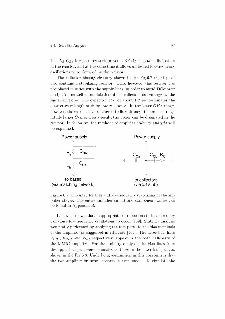
6.4. Stability Analysis 97
The LB-CBa low-pass network prevents RF signal power dissipationin the resistor, and at the same time it allows undesired low-frequencyoscillations to be damped by the resistor.
The collector biasing circuitry shown in the Fig.6.7 (right plot)also contains a stabilizing resistor. Here, however, this resistor wasnot placed in series with the supply lines, in order to avoid DC-powerdissipation as well as modulation of the collector bias voltage by thesignal envelope. The capacitor CCa of about 1.2 pF terminates thequarter-wavelength stub by low reactance. In the lower GHz range,however, the current is also allowed to flow through the order of mag-nitude larger CCb, and as a result, the power can be dissipated in theresistor. In following, the methods of amplifier stability analysis willbe explained.
to bases
(via matching network)
LB
RB
CBa
Power supply Power supply
to collectors(via /4 stub)
CCa
CBb R
CC
Cb
Figure 6.7: Circuitry for bias and low-frequency stabilizing of the am-plifier stages. The entire amplifier circuit and component values canbe found in Appendix B.
It is well known that inappropriate terminations in bias circuitrycan cause low-frequency oscillations to occur [169]. Stability analysiswas firstly performed by applying the test ports to the bias terminalsof the amplifier, as suggested in reference [169]. The three bias linesVBB1, VBB2 and VCC respectively, appear in the both half-parts ofthe MMIC amplifier. For the stability analysis, the bias lines fromthe upper half-part were connected to those in the lower half-part, asshown in the Fig.6.8. Underlying assumption in this approach is thatthe two amplifier branches operate in even mode. To simulate the

98 Chapter 6. InP HBT E-band Power Amplifier Design
stability of the power stage, the test ports were applied to the supplyterminals VBB2 and VCC as indicated. The driver stage was tested bymoving the Port 1 to VBB1.
50 50
Port 1 Port 2
VCC
VBB2
VCC
VBB1
VBB2
VBB1in out
Figure 6.8: Setup for K-factor simulations with test ports connectedto the bias lines.
In this analysis the driver stage showed unconditional stability,however K-factor was only about 1.2 in the sub-GHz range. Thepower stage turned out to be potentially unstable, with K-faktorfalling below unity in frequency range 1.3-6 GHz, as indicated in theFig.6.9.
1.00G 10.0G100.M 100.G
1
2
3
4
5
6
7
0
8
Sta
bili
ty fa
cto
r(K
)
0.1 1 10 100
Frequency [GHz]
Figure 6.9: K-factor simulated in the setup from the Fig.6.8 before(-) and after (-o-) inclusion of the stabilizing resistors.
Input and output stability circles obtained at 3 GHz are plot-ted in the Fig.6.10. The regions inside the circles indicate rangesof impedances that will cause oscillations, when applied to the corre-sponding bias lines. Position of the stability circles on the Smith-chartsuggests that large bypass capacitors in series with parasitic induc-tances, could give rise to the parasitic oscillations.
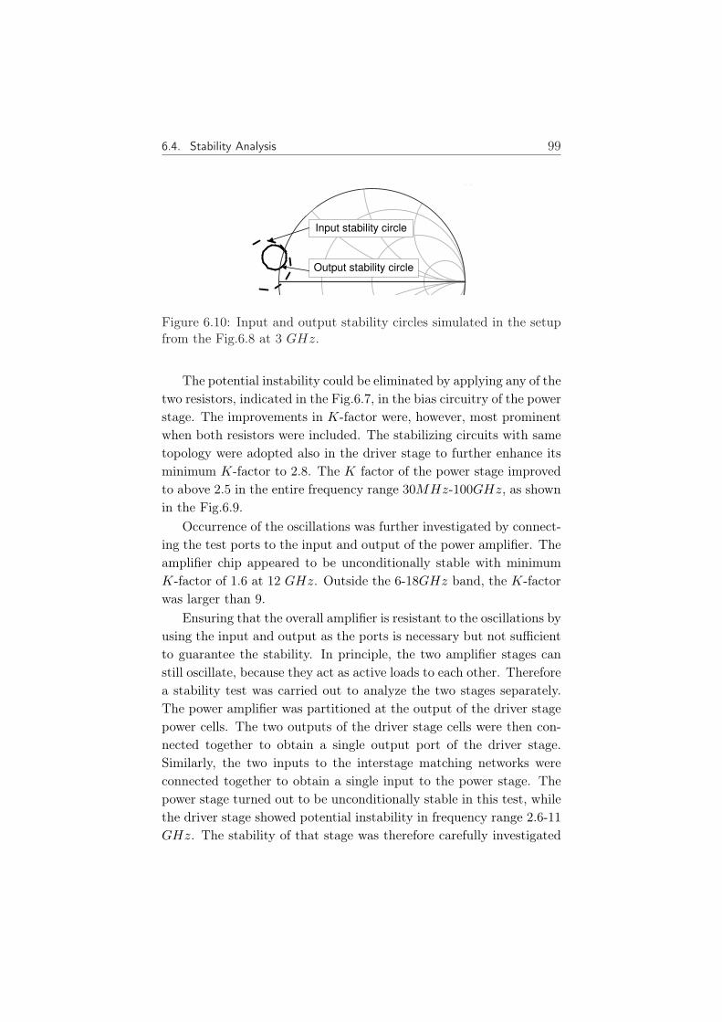
6.4. Stability Analysis 99
Input stability circle
Output stability circle
Figure 6.10: Input and output stability circles simulated in the setupfrom the Fig.6.8 at 3 GHz.
The potential instability could be eliminated by applying any of thetwo resistors, indicated in the Fig.6.7, in the bias circuitry of the powerstage. The improvements in K-factor were, however, most prominentwhen both resistors were included. The stabilizing circuits with sametopology were adopted also in the driver stage to further enhance itsminimum K-factor to 2.8. The K factor of the power stage improvedto above 2.5 in the entire frequency range 30MHz-100GHz, as shownin the Fig.6.9.
Occurrence of the oscillations was further investigated by connect-ing the test ports to the input and output of the power amplifier. Theamplifier chip appeared to be unconditionally stable with minimumK-factor of 1.6 at 12 GHz. Outside the 6-18GHz band, the K-factorwas larger than 9.
Ensuring that the overall amplifier is resistant to the oscillations byusing the input and output as the ports is necessary but not sufficientto guarantee the stability. In principle, the two amplifier stages canstill oscillate, because they act as active loads to each other. Thereforea stability test was carried out to analyze the two stages separately.The power amplifier was partitioned at the output of the driver stagepower cells. The two outputs of the driver stage cells were then con-nected together to obtain a single output port of the driver stage.Similarly, the two inputs to the interstage matching networks wereconnected together to obtain a single input to the power stage. Thepower stage turned out to be unconditionally stable in this test, whilethe driver stage showed potential instability in frequency range 2.6-11GHz. The stability of that stage was therefore carefully investigated

100 Chapter 6. InP HBT E-band Power Amplifier Design
using the mapping circles calculated at the power-stage input. Themapping circles calculated in ADS represented contours of impedancesseen into the input of the power stage, when its output was terminatedby a range of impedances lying on unity-magnitude reflection circle.Results of this simulation are illustrated in the Fig.6.11. It can beconcluded from the figure that there is no overlap between the out-put driver-stage stability circles with the power-stage mapping circles.Hence, the driver stage remains stable for any passive load applied tothe output of the amplifier chip. The same kind of test was performedby using the bias lines as the output ports for the power stage. Nei-ther in this case the two groups of circles overlapped. Using the sameapproach, it was finally also ensured that the input stability circles ofthe power stage do not overlap the mapping circles of the driver-stageoutput.
Stability circles
(driver-stage output)
Mapping circles
(power-stage input)
2.5 GHz
16.5 GHz
16.5 GHz
2.5 GHz
Figure 6.11: Output stability circles of the driver stage and input map-ping circles of the power stage to test the driver stage stability. Thesimulation results are presented for the frequency range 2.5-16.5GHzin a 2GHz step.
6.4.2 Odd-Mode Stability
Another stability test was performed such that the two amplifier brancheswere excited in odd mode and oscillations were observed. Fig.6.12 il-lustrates the simulation setup in which Transient Simulation tool inADS was used. The two voltage sources each generate a single pulsewith opposite polarity to excite the oscillations in the odd-mode.

6.4. Stability Analysis 101
If the oscillations decrease with time and vanish, the circuit is re-garded to be stable to this mode. The results of such a study arepresented in Fig.6.13, where the voltage time waveforms in the twoamplifier branches are shown as a function of time. It can be seen thatwithout the stabilizing resistors, an odd mode oscillation will poten-tially develop and will lead to strong oscillations at about 11.7 GHz.Introducing a 10Ω resistor Rodd eliminates the instability problem.
Rodd
10
Input
match
/combiner 50
Output
match
/
combinerVB2
VB1
Interstage
match
50
Interstage
match
Figure 6.12: Setup for time-domain simulations of the odd-mode os-cillations.
20 40 60 80 100 120 140 160 180 200 220 2400 260
793
794
795
796
792
797
VB
1,
VB
2
[mV
]
time [psec]
20 40 60 80 100 120 140 160 180 200 220 2400 260
790
795
800
785
805
time [psec]
VB
1,
VB
2
[mV
]
VB1
VB1
VB2
VB2Without stabilizing resistor
With stabilizing resistor
Figure 6.13: Time evolution of an odd-mode excitation to test thestability of the amplifier.
It should be pointed out that only the driver stage was responsi-ble for the odd-mode instability. The unstable operation was namelyobtained even if the power stage cells and output combiner were re-moved from the simulation setup. The oscillation loop in the driverstage is actually formed by the two power cells, the input power split-

102 Chapter 6. InP HBT E-band Power Amplifier Design
ter and the two stubs. This loop path is indicated by the dashed linein the Fig.6.6). On contrary to that, the power stage behaved stable,if the driver cells were removed. Input side of the power stage seesthe 209fF blocking capacitor Cs2 and the lossy bias network, whichdamps the oscillations in that stage. As a result, the Rodd was onlyeffective in damping the oscillations if inserted in the circuit on theleft hand side of the Cs2, as it was shown in the Fig.6.6.
6.5 Amplifier Performance
Photograph of the circuit fabricated in the InP HBT coplanar processfrom Alcatel-Thales III-V Lab is shown in the Fig.6.14. The circuitwas laid out symmetrically around horizontal center-axis to assureequal operation of the two half-parts. The chip area measures 1.45×1.25 mm2.
VBB1 VBB2 VCC
IN OUT
VBB1 VBB2 VCC
Figure 6.14: Photograph of the InP HBT two-stage power amplifierMMIC.

6.5. Amplifier Performance 103
On-wafer S-parameters of the power amplifier were measured us-ing an Anritsu ME7808B Broadband Vector Network Analyzer (VNA),and 110GHz coaxial probes, as illustrated in the Fig.6.15. Ground-signal-ground (GSG) Infinity Probe was used for contacting the ampli-fier’s input pad, while the output was contacted with the Picoprobe.DC-power was applied to the MMIC using power probes.
Network-analyser
ME7808B
MMIC
GS
GG
SG
PPPPP
PPPPPPPP
VBB1
VBB2
VCC
in out
VBB1
VBB2
VCC
Figure 6.15: S-parameter measurement setup.
Measured small-signal gain and input/output return losses arecompared with the data predicted by ADS in the Fig.6.16. The datawere obtained at total collector current 320 mA and collector voltage2.4 V . From the measured S21 magnitude it can be concluded thatthe 3dB bandwidth is 60-95GHz, which is equivalent to 45% relativebandwidth. The input matching network was optimized in simula-tions to yield minimum reflection at the center frequency 73.5 GHz
as indicated in the Fig.6.16. The measured return losses are, however,significantly shifted upwards in frequency compared to the simulatedones. Maximum value of S21 magnitude therefore also occurs at higherfrequency than predicted. The simulated and measured S21 have peakvalues of 10.4 dB at 68 GHz and 7.5 dB at 77 GHz respectively. The
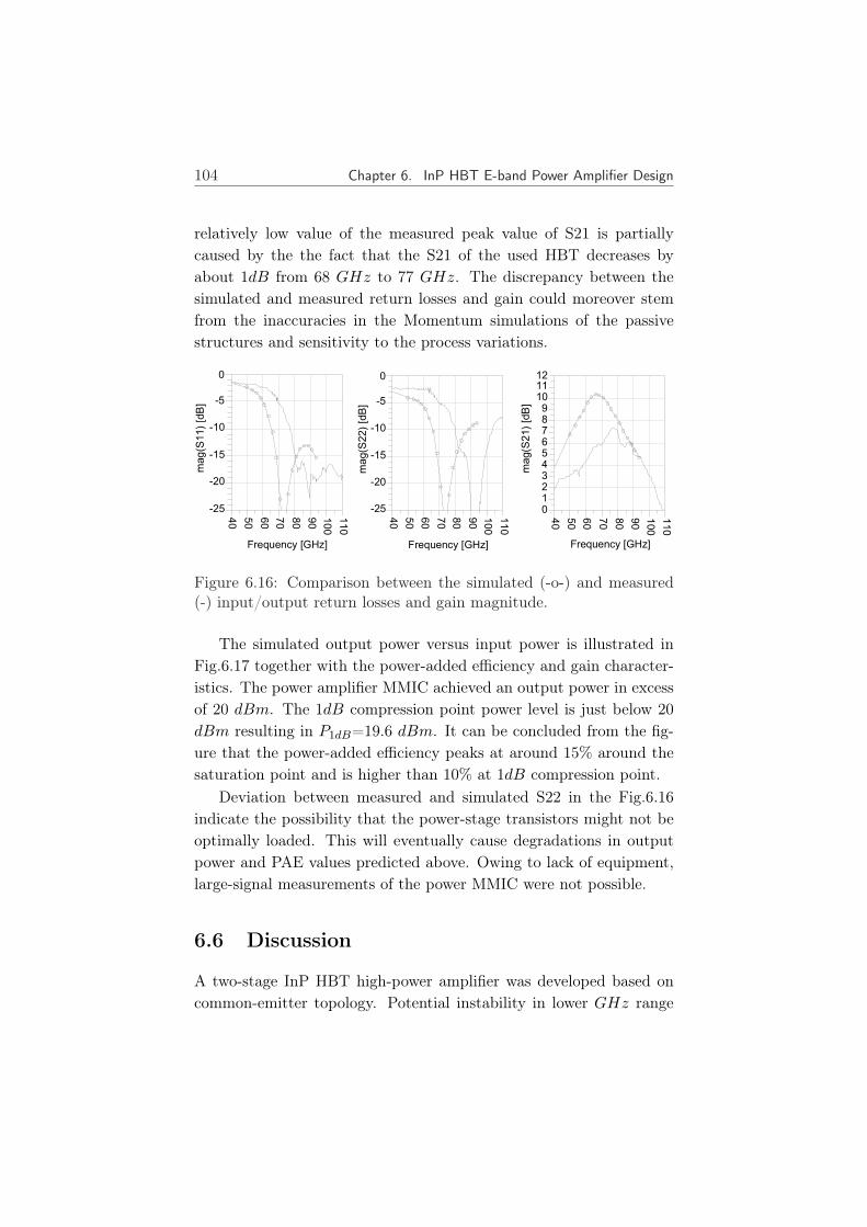
104 Chapter 6. InP HBT E-band Power Amplifier Design
relatively low value of the measured peak value of S21 is partiallycaused by the the fact that the S21 of the used HBT decreases byabout 1dB from 68 GHz to 77 GHz. The discrepancy between thesimulated and measured return losses and gain could moreover stemfrom the inaccuracies in the Momentum simulations of the passivestructures and sensitivity to the process variations.
50
60
70
80
90
10
0
40
11
0
-20
-15
-10
-5
-25
0
Frequency [GHz]
50
60
70
80
90
10
0
40
11
0
-20
-15
-10
-5
-25
0
Frequency [GHz]
50
60
70
80
90
100
40
110
123456789
1011
0
12
Frequency [GHz]
ma
g(S
22
) [d
B]
mag
(S11
) [d
B]
ma
g(S
21)
[dB
]
Figure 6.16: Comparison between the simulated (-o-) and measured(-) input/output return losses and gain magnitude.
The simulated output power versus input power is illustrated inFig.6.17 together with the power-added efficiency and gain character-istics. The power amplifier MMIC achieved an output power in excessof 20 dBm. The 1dB compression point power level is just below 20dBm resulting in P1dB=19.6 dBm. It can be concluded from the fig-ure that the power-added efficiency peaks at around 15% around thesaturation point and is higher than 10% at 1dB compression point.
Deviation between measured and simulated S22 in the Fig.6.16indicate the possibility that the power-stage transistors might not beoptimally loaded. This will eventually cause degradations in outputpower and PAE values predicted above. Owing to lack of equipment,large-signal measurements of the power MMIC were not possible.
6.6 Discussion
A two-stage InP HBT high-power amplifier was developed based oncommon-emitter topology. Potential instability in lower GHz range

6.6. Discussion 105
-20 -10 0 10-30-20
20
30 10
20 9P
OU
T [
dB
m]
PA
E [
%]
GA
IN [d
B]
10 8
0 7
-10 6
5
PIN
Figure 6.17: Simulated output power, PAE and transducer gain forthe power amplifier MMIC at 73.5 GHz.
appeared in the bias-line analysis. Insertion of resistive loadings in thebias circuitry resulted in minimum K of 2.5 in the entire frequencyrange, without compromising high-frequency gain. A method for sim-ulation of the odd-mode oscillations between the combined transistorshas been presented and successfully applied to stabilize the driver stageusing a single resistor.
The developed four-transistor power cell provides nearly equal com-bining characteristics and load impedance to all four transistors. Theamplifier exhibits a peak small-signal insertion gain of 7.5 dB at around77 GHz. The gain falls by 3dB at 60GHz and 95GHz. The mea-sured return-loss characteristics were remarkably upward-shifted infrequency compared to the simulated ones, which also caused gain re-duction. Whether these deviations arose from sensitivity to the processparameters or inaccurate modeling will be investigated in the future.Moreover, implementation of the CB or cascode configurations will bereconsidered more deeply aiming at higher gain per amplifier stage.
The simulated output power in 1dB compression is 95 mW or19.6 dBm, while the saturated power is in excess of 100 mW . Theachieved power added efficiency peaks at around 15% around satura-tion point. The reported results demonstrate the possibilities to utilizeATL InP HBT processes in the design of mm-wave power amplifiers.The achieved power and PAE data represent record performance levelsfrom an InP HBT power MMIC operating above 50GHz.

Chapter 7
InP HBT mm-wave QVCOdesign
Millimeter-wave systems such as E-band communication transceiversrequire high-performance oscillators for high-frequency signal genera-tion. Quadrature voltage controlled oscillators are useful for quadra-ture (de)modulators, in direct-conversion transceivers and for imagereject mixers. The previous two chapters of this thesis demonstratedapplicability of ATL’s InP HBT technology for design of millimeterwave PAs. Same technology was used to implement mm-wave quadra-ture voltage controlled oscillator, described in this chapter.
High-frequency QVCOs are mainly realized as two identical oscil-lators interconnected by coupling circuitry. The two oscillators can berealized as ring oscillators [204], taking up less die area and havingwider tuning range as compared to LC-tank oscillators. However, su-perior phase-noise performance of the LC-oscillators makes them moreattractive in many communication systems. The LC-oscillator conceptwas adopted in this work.
One way to realize frequency tuning in a LC-QVCO is to imple-ment varactors [46,205], as in the most single VCOs. Microwave [118]and mm-wave [206, 207] VCOs can suffer from low quality factor ofthe varactors and the associated parasitic capacitances that degradephase-noise performance and diminish tuning range. An alternativesolution for QVCO tuning is a variation of coupling factor between
106

107
the oscillators [45, 47]. Because high-quality varactors were not avail-able in the used InP HBT process, variation of the coupling factor wasadopted. Interaction of this tuning mechanism with bias-dependentcapacitances of the HBTs will also be investigated.
Very high oscillation frequencies demanded by mm-wave systemsnecessitates miniaturization of LC-resonators [46]. High-frequency os-cillator performance becomes therefore highly dependent on layoutand transistor parasitics. In this chapter, parasitic effects of an inter-connecting line inductance and of a base resistance will be analyzedin a feedback model of a cross-coupled mm-wave LC-oscillator. Theanalysis will also encompass a resonator, which is intentionally iso-lated from the device using an additional capacitor. This technique iscommonly applied in cross-coupled mm-wave oscillators [117,119] andalso in lower microwave range [118].
A simple cross-coupled differential oscillator architecture has beensuccessfully implemented in a CMOS-based mm-wave VCO [206] aswell as in a QVCO [45]. However, a mm-wave QVCO based on thisarchitecture, further in this text referred to as ’simple’ architecture,has not yet been demonstrated in any bipolar technology. A 28GHz
SiGe HBT QVCO [49] was based on a cross-coupled topology, whichincludes an additional emitter-follower transistor pair in the feedbackpath of each oscillator. A possible advantage of this ’buffered’ ap-proach is a separation of the resonator from the transistor parasitics,which could enhance the achievable oscillation frequency and improvephase-noise. However, an additional loop-delay and noise introducedby the emitter followers might have negative impact on the perfor-mance. Moreover, capacitively loaded emitter followers might becomeunstable [208], which could cause parasitic oscillations in a QVCO.
This chapter explores properties of the ’simple’ and the ’buffered’oscillator architectures, based on the used InP HBT process. The twosingle oscillators will firstly be treated using feedback theory. Theanalysis and linear simulations will be performed based on their sim-plified small-signal equivalent circuits. From these results, behavior ofQVCOs based on the two oscillator types will be inferred. Non-lineardevice models will then be employed to verify the performance of thetwo QVCOs in a nonlinear simulator. Potential instability risk due to

108 Chapter 7. InP HBT mm-wave QVCO design
the buffers in the feedback path will be investigated. The implementedQVCO design based on the buffered topology will be presented, alongwith the experimental results and the procedures applied to verify theachieved tuning range and power performance.
7.1 Principle of Operation of a QVCO
Block diagram of the realized QVCO is shown in the Fig.7.1. Barkhausencriterion imposes the phase-shift around an oscillator loop to be zeroor integer multiple of 360 at the oscillation frequency. To fulfill thisrequirement, phase offset between the differential outputs of the twoidentical oscillators has to be 90, and one of the outputs has to beinverted, as indicated in the figure.
OSC1
IN+ OUT+
IN- OUT-
OSC2
IN+ OUT+
IN- OUT-
0o90o
180o
-90o90o
-90o
Figure 7.1: Block diagram showing two identical oscillators coupled ina QVCO loop.
QVCOs employing simple oscillator topology from the Fig.7.2 (left)as the building block, has been subject of theoretical analysis by sev-eral authors [209–212]. The simple QVCO has been described as achain of transconductors followed by parallel RLC-networks connectedin a loop. The cross-coupled pair of the core transistors Tcr, andvirtual ground existing between their emitters ensure differential op-eration. The output transistors Tout serve to drive 50Ω equipment.Coupling transistors Tcp provide coupling from another identical os-cillator. Quadrature generation is established by connecting the IN±and OUT± terminals of the two oscillators in a manner describedby the Fig.7.1. As a result, Tcr and Tcp transistors are excited bybase-emitter voltages which are 90 out of phase. Thus, the signalcurrents, icr and icp, generated by the two respective transistors, arein quadrature as well, as depicted in the Fig.7.2 (right). Magnitudesof the two currents are proportional to the fundamental components

7.1. Principle of Operation of a QVCO 109
of the respective large-signal transconductances Gm,cr and Gm,cp. To-tal current itot injected into the resonator is equal to icp + icr. Inthis simplified analysis it was assumed that the resonator can be rep-resented by a parallel RLC-network (resistor is not shown), and nocurrent flows into the base of another transistor. This detail will beincluded in the analysis in section 7.2.
OUT+
IN- IN+
Tout
OUT-
Loadout -
Load
out +T
crT
cp
Icr
Icp
icr
icp
icp
=Gm,cp
Vbe,cp
itot
icr =
Gm
,cr V
be
,cr
Figure 7.2: Left: Conceptual diagram of a simple cross-coupled oscil-lator, as a building block of a QVCO. Right: A phasor representationindicating signal currents in the devices.
A single oscillator operates at resonance frequency of the LC-tank,where the phase of its impedance function is zero. Because itot isphase-shifted as compared to the single oscillator case, the QVCOhas to operate away from the tank resonance to maintain zero-phaseshift around the loop. This frequency departure increases with thetransconductance ratio
m =Gm,cp
Gm,cr(7.1)
which has been defined as a coupling factor of a QVCO [209]. Fre-quency tuning can be be accomplished through variation of DC-currentsIcr and Icp that control the two respective transconductances.
In an oscillator that do not oscillates at the resonance frequencyof the LC-tank, phase ∆ϕ of the tank impedance function at the os-cillation frequency ω0 would not be zero. Near the resonance ∆ϕ issmall, and an effective resonator quality factor Qeff can be estimatedfrom the slope of the phase characteristic dϕ/dω at ω0 [213],
Qeff ' ω0
2dϕ
dω. (7.2)

110 Chapter 7. InP HBT mm-wave QVCO design
Because the phase slope is steepest at the resonance frequency,Qeff decreases with increasing phase deviation ∆ϕ. For large valuesof ∆ϕ, approximation to the Qeff is [214]
Qeff ' Q cos(∆ϕ). (7.3)
where Q is quality factor at the resonance frequency. Again it followsthat Qeff decreases as ∆ϕ departs from zero.
Leeson’s equation (3.2) showed that LC-oscillators benefit fromhigh Q with regards to the phase noise. Hence, the phase noise ofa single oscillator increases as the oscillation frequency departs fromthe resonance frequency. The same is true for quadrature oscillators.Phase-noise in the simple model of a QVCO, based on a parallel RLC-tank, differs by factor [1 + m2]/2 from the single oscillators phase-noise [209], where m is given in the eq.(7.1).
7.2 Small-Signal Approximation of the SimpleOscillator
The simple cross-coupled oscillator topology from the Fig.7.2 havebeen successfully exploited in a 43GHz CMOS QVCO, tuneable by abias-dependent coupling [45]. This section explores the performancelimiting factors of an HBT-based simple oscillator operating in a QVCO.Open-loop equivalent circuit of the oscillator will be developed basedon small-signal equivalent representation of the used InP HBT andthe resonator circuit. The equivalent circuit will identify main limi-tations of the transistor in the simple oscillator topology. After that,open-loop transfer functions will be derived for three oscillator cir-cuits, in order to explain the impact of the base resistance, inductanceof an interconnecting line and an additional coupling capacitor, whichcan enhance the loop gain and the oscillation frequency. Finally, anopen-loop simulation will be performed on the equivalent circuit.

7.2. Small-Signal Approximation of the Simple Oscillator 111
7.2.1 Simplified Equivalent-Circuit Representation
A closed-loop equivalent circuit representation of the simple oscillator,illustrated in the Fig.7.3 a), is based on small-signal elements of thetransistor and resonator circuit. Element values of the HBT, listedin Table 7.1, were extracted from the large-signal model of the de-vice presented in [139]. Parallel connection of the elements Lr, Cres
and Rr represents the inductor implemented in the QVCO, describedin sections 7.4 and 7.5. The inductor elements were extracted usingEM-simulation software Momentum. The Rr is omitted in the equiv-alent circuit since the overall Q is strongly dominated by the lossesoriginating from the transistors, as will be explained shortly. Thecollector-emitter fringing capacitance Cce is summed with Cr into asingle element Cr as shown in the Fig.7.3 a). Contributions of theexternal region of the device to the total Cbc was 80%. To simplifythe model Cbc was therefore applied externally as indicated.
gm
Vbe
Lr
Rbt
Cbc
+
Vbe-
Cbet
Rbt
Cbet
a)
b)
Cbet
c)
2Cbc
+Cr
d)
Rbt
Cbet
4Cbc
+Cr
Cr
Cr
+
V’be-
Cbc
2Cbc
Lr
Lr
Lr
gm
Vbe
gm
Vbe
gm
Vbe
Rbt
+
Vbe-
+
Vbe-
+
Vbe-
+
V’be-
+
V’be-
Figure 7.3: Transformation of the simple cross-coupled oscillator fromthe closed-loop a) to the open-loop representation b). Diagrams c)and d) are equivalent representations of the diagram b).

112 Chapter 7. InP HBT mm-wave QVCO design
ValueParameter Passives Ic = 1mA Ic = 3mA Ic = 5mA
Cbc[fF ] 5.5 4 3.5Cbe[fF ] 39 61 79
Rb[Ω] 44 42 41gm[mS] 30 92 152Cce[fF ] 7.9Lr[pH] 115Rr[Ω] 849
Cres[fF ] 4.1
Table 7.1: Small-signal element values of the 3×1.5µm2 device biasedat Vce = 0.8V , and parasitics representing the resonator inductor at50 GHz.
In the closed-loop model of the Fig.7.3 a), one half-part of the os-cillator loop is represented by the extracted components, and anotheridentical half-part by the ideal transformer having transformation ratioN = −1. This representation is valid because the voltage waveformsacross the two inductors in the Fig.7.2 are 180 out of phase.
The transformer output looks into the base terminals of the coretransistor Tcr, coupling transistor Tcp in another oscillator, and theoutput buffer Tout. Since same bias is assumed for the three transistors,their Cbe and Rb are same. Furthermore, the Cbe-Rb networks of Tcr
and Tcp appear to be in parallel, since their emitters are at virtualgrounds. Under assumption of unilateral Tcr and Tcp (neglecting theirCbc), their Cbe and Rb were merged into single RC-network, Cbet =2Cbe and Rbt = Rb/2, as shown in the Fig.7.3 a). This approach wouldnot make sense in an equivalent circuit of a QVCO. However, purposeof this unilateral assumption is only to approximate the additionalloading of Tcp on the resonator in a single oscillator of a QVCO.
Input admittance of the output buffer driving 50-Ω load is
Yin,Tout = jωCbc +(
50 + Rb + Rb +1 + gm(50 + Rb)
jωCbe
)−1
(7.4)
= jωCbc + (102 + 1/(jω0.15Cbe))−1 , (7.5)

7.2. Small-Signal Approximation of the Simple Oscillator 113
where emitter access resistance is Rb = 10Ω and values for Rb andgm at 3mA from the Table 7.1 have been assumed. After insertionof the Cbe and Cbc from the Table 7.1 into the eq.(7.5), it can beshown that the impedance |1/Yin,Tout | is order of magnitude largerthan impedance of the Rbt-Cbet series network. Hence, relatively lowsignal current flows into the base of Tout. Therefore, it is not likely thatTout would significantly degrade the oscillation frequency. This wasalso proven by harmonic balance simulations of this oscillator, namely,oscillation frequency only increased by 4% after removing the Tout. Itis moreover easily seen that the quality factor of the second term ofthe eq.(7.5), Q=1/(102× 0.15ωCbe) is relatively high as compared tothe Q of the dominating Rbt-Cbet network, Q=1/(42ωCbe). Hence,oscillation frequency and total quality factor are dominated by theRbt-Cbet network.
At the oscillation frequency of 50 GHz, the inductor Q was 23.5,which is around 19 times higher than Q of the Rbt-Cbet series networkat 3mA. Therefore, the inductor parasitic resistance is also omittedin the equivalent circuit.
In the Fig.7.3 b) the oscillator elements are rearranged such thatthe reference plane for opening the loop at the B-E junction becomesapparent.
After opening the loop, a Miller theorem was applied on Cbc. Thiscomponent can be replaced by two equivalent capacitors of double sizeon each side of the transformer since
YMill,in = jωCbe(1−N) = jω2Cbe (7.6)
YMill,out = jωCbe(1− 1/N) = jω2Cbe, (7.7)
where N = −1. The obtained circuit looks like in the Fig.7.3 c).According to the theory from [215], the elements on the right side ofthe transformer having N = ±1 can be moved to the left side withoutchanging their values. After 2Cbc, Rbt and Cbet were moved to theleft side of the transformer, the transformer was removed, and thecurrent source has reversed direction in order to preserve the sign ofthe voltage transfer function. After these rearrangements the diagrambecomes that depicted in the Fig.7.3 d).

114 Chapter 7. InP HBT mm-wave QVCO design
When quadrupled by the Miller effect, Cbc grows into 20fF rangeand becomes comparable to Cbe=61fF . Cbc would become even moreharmful if placed in the intrinsic transistor since it would be chargedthrough the Rb. In the present circuit it limits only the oscillationfrequency, but main performance degradation comes from the largecapacitance Cbe, as well as CbeRb time constant, which governs thetotal Q of the oscillator. The quality factor of the Cbe − Rb networkis 1.25 at 50GHz.
Maximum oscillation frequency of a device, fmax =√
ft/(8πCbcRb),is often regarded as the key parameter for high performance oscillatordesign. However, fmax can be high because Cbc is low - but Rb mightstill be high. Low Cbc would increase fmax also through the expressionfor the cut-off frequency given in the eq.3.6. Similarly, ft alone is not aguarantee for a good phase-noise since it disregards Rb. Therefore, fora high performance mm-wave QVCO of this type, both FOMs mustbe high, and CbeRb time constant should be low.
7.2.2 Parasitic Effects and Modifications in a ResonatorStructure
Simplified equivalent model from the Fig.7.3 d) will be extended herein order to explain influence of various parasitic elements and modifi-cations that might occur in the simple type of oscillator. The extendedversion of the equivalent diagram, shown in the Fig.7.4, includes nowalso Rr, which is assumed to represent a resonator loss, and Xs whichwill either represent a parasitic inductance of an interconnecting lineor a series capacitance, which serves to enhance the resonator Q. TheRs series resistor represents the base resistance. To simplify the an-alytical expressions, impact of the three elements will be analyzedseparately, through three cases.
Case 1: Xs = 0 Assuming no series reactances, the open-loop trans-fer function can be written as
7.2. Small-Signal Approximation of the Simple Oscillator 115
V′be
Vbe=
gm
RsCp
(1Lr
− ω2Cr
)
︸ ︷︷ ︸Gpeq
+sCpRsRr
+(
1sLr
+ s(Cr + Cp) + 1Rr
) .
(7.8)where s = jω. The eq.(7.8) suggests that the passive elements couldbe represented by a parallel RLC-network at angular frequency ω. Therightmost term in the denominator in the parenthesis is an admittance,equivalent to the four shunt elements in the absence of the Rs. Thesecond term is an additional capacitive contribution arising from Rs.First term is an additional equivalent conductance, Gpeq, accountingfor the losses introduced by Rs. Using the values from the Table 7.1,it follows that Rs/Rr ' 0.05 << 1. Hence, the second term representsa very small capacitance in comparison to the dominant (Cr + Cp),meaning that Rs will not significantly slow down the oscillator. In thediscussed simple oscillator, main loss comes from the base resistanceRs, and thus Gpeq >> 1/Rr. Under these assumptions, the qualityfactor and the oscillation frequency can be estimated as
Q =1
ω0LrGpeqand ω0 =
(√Lr(Cr + Cp)
)−1
. (7.9)
Substitution of Gpeq from eq.7.8, into eq.7.9 yields
Q =Cp + Cr
RsC2pω0
=1
ω30RsC2
pLr. (7.10)
Assume now a device with given Rs and Cp. From the first expres-sion in eq.(7.10), it follows that increasing the tank capacitance Cr,while keeping ω0 constant, would increase the Q. This is only possibleif the inductance is reduced. Same can be deduced from the secondexpression - trying to increase Lr, while keeping ω0 and transistor pa-rameters constant, would lead to reduction of Q. In other words, in abipolar oscillator, if the base series resistance strongly dominates theoverall Q, it is more beneficial to have large tank capacitance than alarge inductance.

116 Chapter 7. InP HBT mm-wave QVCO design
Another interesting detail in eq.(7.8) is that Gpeq decreases withfrequency. Due to that fact, peak in magnitude of the transfer functionwill be shifted up in frequency, away from the point where the phasecrosses zero.
Lr
Rs
Cp
Crg
mV
be
+
Vbe-
+
V’be-
Xs
Rr
Figure 7.4: Open-loop equivalent circuit of the simple oscillator ex-tended for analysis of various parasitic effects.
Case 2: Xs = jωLs will now be inserted in the circuit of Fig.7.4to analyze impact of an interconnecting inductance Ls on the simpleoscillator performance. Neglecting the small sCpRs/Rr term, as inCase 1, the transfer function becomes
V′be
Vbe' gm
Gpeq + LsCp
Rr+ sLsCp
(1
Lr− ω2Cr
)+
(1
sLr+ s(Cr + Cp) + 1
Rr
) .
(7.11)Again, in the absence of the parasitic element Ls, the parallel RLCterm on the right side of the eq.(7.11) would determine the oscillationfrequency ω0. The third term represents an additional parallel sus-ceptance coming from Ls. Possible new zeros in the phase responsecould be calculated by solving a 4th-order equation. Most interestingis however the shift of ω0 due to Ls. Since Cr < Cr + Cp, the thirdterm is positive near ω0, that is, the term represents an additionalpositive shunt capacitance, thereby reducing ω0. Therefore, if a highoscillation frequency is desirable in the simple topology, base-terminalsshould be connected to the resonator circuit using shortest possible in-terconnects. This principle can also be applied to the other types ofoscillators when connecting a large capacitance to the resonators.
The second term of eq.(7.11) accounts for the additional loss com-ing from Ls. The first term is the loss contribution from the baseresistance, already described in eq.(7.8). It can be intuitively seenthat Ls does not strongly influence the Q, since both the conductive

7.2. Small-Signal Approximation of the Simple Oscillator 117
and the capacitive contributions from Ls (2nd and 3rd term, respec-tively) are proportional to Ls.
Case 3: Xs = 1/(jωCs) . Transfer function of that version of theoscillator circuit, written in form compatible with the previous twocases, is
V′be
Vbe' gm
Gpeq + Cp
Cs
(1
sLr+ sCr + 1
Rr
)+
(1
sLr+ s(Cr + Cp) + 1
Rr
) .
(7.12)The small sCpRs/Rp term is again omitted for simplicity. As in thetwo previous cases, the rightmost term of the equation represent theadmittance function in the absence of the series elements. The secondterm acts as an additional parallel RLC-network, and is proportionalto 1/Cs. The oscillation frequency is determined by the total capaci-tance across the Lr,
ω0s =
(√Lr
(Cr +
CsCp
Cs + Cp
))−1
. (7.13)
Small value of Cs offers several advantages with respect to highoscillation frequency and Q. First, oscillation frequency goes up andapproaches ω0 = 1/
√LrCr. Second, when the second and the third
term of the eq.(7.12) are added, it is seen that the total equivalentinductance of the parallel circuit representation decreases, and totalequivalent capacitance increases. Third, as the oscillation frequencyω0s approaches ω0, Gpeq vanishes, as shown in the eq.(7.8). These threefacts count towards higher total Q. Unfortunately, as Cs decreases,the 1/Rr term in the second term of the eq.(7.12) grows as well andbecomes comparable to Gpeq. For a very small Cs, the magnitude ofthe transfer function will be dominated by the Cp/(CsRr), which canbe seen as a magnified resonator conductance. A value of Cs at whichthe two conductances, Gpeq and Cp/(CsRr), are equal, is given by
Cs =Lr
(Cr + Cp +
√(Cr + Cp)
2 + 4RsRrCpCr
Lr
)
2RsRrCp. (7.14)

118 Chapter 7. InP HBT mm-wave QVCO design
Below this value of the series capacitance, Cp/(CsRr) conductancecomponent will more and more rapidly degrade the magnitude of thetransfer function.
7.2.3 Simulated Open-Loop Response
Frequency tuning mechanism of a QVCO based on the simple oscilla-tor topology can be inferred from a plotted open-loop voltage trans-fer function of the single oscillator. For this simulation, a simplifiedsmall-signal device model described in section 7.2 was extended byincorporating the access resistances in series with emitter, Rb = 10Ω,and collector, Rc = 11Ω. The open-loop diagram is formed by a singledevice, and a resonator, similarly to the Fig.7.3 d). Resonator loss Rr
was included as well. Simulated transfer function assuming 3mA biascurrent in the core devices is shown in the Fig.7.5.
50 1000 150
1
2
3
4
0
5
-90
0
90
-180
180
freq [GHz]
phaseV
’be
/ Vb
e magV
’ be
/ V
be
Figure 7.5: Open-loop response of the small-signal model of the simplecross-coupled oscillator.
The oscillation frequency, f0 ' 50GHz, is where the phase re-sponse crosses zero. Magnitude of the transfer function is ∼4, whichis sufficient for reliable oscillation startup. As expected from the sim-plified analysis in section 7.2.2, peak in magnitude of the transferfunction is shifted up away from f0. It was also confirmed by thesimulations that the base resistance indeed had no impact on the os-cillation frequency - it only flattened the phase response and degradedthe gain.

7.2. Small-Signal Approximation of the Simple Oscillator 119
Low-frequency phase response deviates strongly from what can beexpected from the simple version of the equivalent circuit from theFig.7.3. According to the eq.(7.8), the phase of that circuit convergesto 90 as the frequency approaches zero. This discrepancy was foundto be caused by the presence of Re. Gain reduction due to Re is∼ 25%.
When coupled into QVCO loop, phase response of the transferfunction would be further flattened, and gain and frequency wouldreduce due to additional loading by the coupling HBT. When Rb washalved and Cbe doubled to account for this approximately as in thesimple model before, f0 reduced to 43GHz and gain became 2.2 only.
In order to tune the oscillation frequency of the QVCO, the cou-pling factor can be varied by changing the bias current either in thecore devices Tcr or the coupling devices Tcp, as explained before. SinceTcp is driven 90 in advance, it can be intuitively seen that the phasecharacteristics in the Fig.7.5 would be shifted upwards when the os-cillator is connected in a QVCO. Consequently, oscillation frequencyhas to increase. Therefore, if both devices inject the current, f0 wouldlie between the two extremes as indicated in the Fig.7.5.
Increase of frequency can be accomplished through the increase ofthe bias current in Tcp, or decrease in Tcr, since both actions wouldincrease the coupling. However, there is an additional tuning mecha-nism in this oscillator, namely, the Cbe increases with current, as canbe concluded from the Table 7.1. In simulation of the small-signalmodel, it was observed that f0 decreased from 55 to 47 GHz whenthe current in Tcr was increased from 1 to 5 mA. If Tcr is used fortuning, it is easily seen that the two tuning mechanisms act in samedirection. This varactor-like effect of Tcr would first of all expand thetuning range. But, even more important is the fact that the frequencyrange where the phase is steepest, and phase noise lowest, would tendto follow the oscillating frequency. On contrary, if current in Tcp isincreased in order to increase the coupling and f0, increase of its Cbe
would counteract that action. Therefore, tuning method by modu-lation of core devices provides wider useful tuning range. This wasproven by harmonic balance simulations which will be described insection 7.4.1.
120 Chapter 7. InP HBT mm-wave QVCO design
It was also attempted to insert a capacitance Cs in series with thebase terminal. Insertion of a 11fF capacitor, calculated using theeq.(7.14), enhanced the oscillation frequency from 50 to 73 GHz, andincreased the gain from 4 to 6. For Cs < 9.5fF gain decreased veryrapidly. This confirmed the usefulness of the eq.(7.14). Implementa-tion of Cs should be seriously considered when designing the simplecross-coupled architecture in a bipolar process.
Another advantage of having Cs lies in the possibility to separatebase and collector bias. In fact, transistor base in the simple oscillatorin the Fig.7.2 is on same potential as collector. Applying a separatebase bias would make it possible to increase the voltage swing. Cs
would be especially beneficial in InP HBT based oscillators, due tolarge voltage swing available, and since the bipolar devices normallyexhibits higher base resistance as compared to resistance of the metalgate of the field effect transistors [211]. Designs employing Cs betweenthe transistor and the resonator circuit have been reported in variousoscillator topologies, frequency bands, and technologies [117–119].
7.3 Small-Signal Approximation of the BufferedOscillator
Another cross-coupled topology employs a pair of emitter-followerbuffers Tfb as depicted in the Fig.7.6. A 28GHz QVCO based on that’buffered’ topology was demonstrated in SiGe HBT technology [49].Variable tank capacitor was used for frequency tuning, with additionalpossibility to modulate the capacitances of the core HBTs. This cir-cuit architecture is implemented in this work, but the coupling factoris used for frequency tuning. In the buffered topology the Tfb isolatesthe resonator from the parasitic loading of the other three devices,Tcr, Tout, and Tcp in another oscillator. This enhances the oscillationfrequency and improves phase noise. The additional phase-shift of thetwo buffers can bring the oscillation frequency away from the tankresonance. Aim of this section is to shed a light on these issues, andto predict behavior of a QVCO based on this oscillator type.

7.3. Small-Signal Approximation of the Buffered Oscillator 121
OUT+IN- IN+
OUT-
Loadout -
Load
out + Tcr
Ifb I
cr Icp
Tfb
TcpT
out
Figure 7.6: Conceptual schematic of the realized buffered oscillatortopology.
7.3.1 Analysis of the Small-Signal Equivalent Circuit
Presence of the pair of feedback buffers Tfb in this type of oscillatorsignificantly complicates loop analysis as well as the analysis of thetuning mechanisms in a QVCO. Simplified open-loop diagram in theFig.7.7 (upper diagram) serves as the starting point for the discussion.The diagram was obtained following the procedure applied in the sim-ple oscillator in the Fig.7.3: one half-part of the circuit was replacedby an ideal transformer, than the loop was opened at the base of thecore transistor. The accumulated loading effect of the core-transistorsTcr and coupling transistors Tcp is described by Rbt and CL as before.
The subsequent analysis process can be subdivided into two essen-tial steps. In the first step another approximation was made, namely,Cbc of the core device was replaced by an equivalent capacitor Cbc,eq,across the inductor, as illustrated in the Fig.7.7 (middle diagram). Inthe second step, illustrated in the Fig.7.7 (lower diagram) Cbe1 of thefeedback buffer was replaced by the two equivalent admittances acrossthat device using Miller theorem. This enabled an additional breakin the loop, useful for understanding this oscillator. The open-looptransfer function can than simply be viewed as a product of the twoinner voltage transfer functions. The first one, Vb1/Vbe, will describethe resonator on the left side. Interesting information in this part isthe resonance frequency and loss which were already treated in the sec-tion 7.2.2 for various types of resonators. Possibility to have a negativeconductance Gbmi will also reflect a risk of potential instability of the

122 Chapter 7. InP HBT mm-wave QVCO design
feedback buffer within the oscillator loop. This could eventually leadto development of a parasitic oscillations or even prevent the oscillatorto start-up in the wanted regime. Transfer function of the right part,V ′
be/Vb1, will provide important information about departure of the os-cillation frequency from the tank resonance, which is relevant for thephase-noise and choice of appropriate frequency tuning mechanism ina QVCO. The two steps will now be described in more details.
Step 1: In section 7.2 it has been shown that Cbc component canbe replaced by two equivalent capacitors on each side of the unitygain transformer, by applying Millers theorem. Following the sameidea, attempts were made to simplify this circuit in a same manner inorder to separate the two voltage transfer functions - Cbc of 4fF wasreplaced by two complex admittances, each connected between one Cbc
terminal and ground. The two complex admittances were tuned so tofit the two transfer functions, Vb1/Vbe and V ′
be/Vb1, of the two circuitsfrom the upper and the middle diagram in the Fig.7.7. What came outof the optimization is a Cbc,eq = 7fF , which merged with Cr in themiddle plot, and an another 11fF capacitance at the output side (notshown). The conductive parts of the two admittances were very high(in a kΩ-range) and are omitted from the diagram for clarity. Usingthis optimized capacitance of 7fF it was possible to fit each of thetwo transfer functions with an accuracy of 5% in magnitude and 5
in phase up to 140GHz (around twice the resonance frequency) andin a range of bias-currents, 2 − 4mA for each device. The results ofoptimization indicate that:
• Cbc of the core device is again among the important contributorsto the total tank capacitance.
• Cbc’s output equivalent of 11fF , on contraty, does not have animportant role in the total phase shift, because the output ofthe Tfb is already heavily loaded by two CE stages, as well asan output buffer stage. Therefore, the 11fF capacitor will beomitted from the subsequent analysis of the total phase shift, andit is omitted in the Fig.7.7. According to the simulations, thisapproximation will offset the phase by 5 at the tank resonance,which will not severely hamper analysis undertaken in Step 2.

7.3. Small-Signal Approximation of the Buffered Oscillator 123
gm
Vbe L
r
1 : -1Vc
Cbc,eq
+Cr
Cbe1
gm1
Vbe1
Vb1 V
e1R
btRb1
Cbc1
gm
Vbe L
r
Vc
gm1
Vbe1
Vb1 V
e1R
LR
b1
Cbc1 G
bmi
Feedback-buffer
Feedback-buffer
Cbmi
Ybmo C
L
Re1
gm
Vbe L
r
1 : -1Vc
+V’
be-
Cbe1
gm1
Vbe1
Vb1 V
e1R
btR
b1
Cbc1
Feedback-buffer
Re1
Cbc
Cr
Cbc,eq
+Cr
CL
CL
+V’
be-
+V’
be-
+V
be-
+V
be-
+V
be-
4 fF19 fF
4 fF
12 fF
19 fF
4 fF
4 fF
Figure 7.7: Equivalent diagram of the buffered cross-coupled oscillator.Up: Open-loop equivalent circuit. Middle: Approximative transfor-mation of Cbc of the core device. Down: Miller transformation of B-Ecapacitance of the feedback buffer. Note that Vbe1 = Vb1 − Ve1.
Step 2: By applying Miller theorem, as described by eq.(7.6-7.7),Cbe1, base-emitter capacitance of the feedback-buffer was transformedinto input and output equivalent admittances, as illustrated by theFig.7.7 (lower diagram). Derivation of the following approximate ex-pressions is presented in Appendix C. The expressions are valid in abias and frequency range 2− 5mA and 30− 70GHz for a 3× 1.5µm2
device. Voltage transfer function used for the Miller transformation isgiven by
A =Ve1
Vb1' gm1 + sCbe1(
gm1 + 1RL
)+ s
(Cbe1 + CL
1+(ωCLRL)2
) . (7.15)

124 Chapter 7. InP HBT mm-wave QVCO design
Applying A as the gain in the Miller transformation of Cbe1 to theinput side, yields
Ybmi = Gbmi + sCbmi (7.16)
' ω2Cbe1
Cbe1RL
− gm1CL
1+(ωCLRL)2
1 + gm1RL+ sCbe1
11 + gm1RL
. (7.17)
The two calculated elements Gbmi and Cbmi are connected as shownin the Fig.7.7 (lower diagram). The conductive element becomes neg-ative, and Tfb becomes potentially unstable if the following relation issatisfied:
gm1
Cbe1>
1RLCL
+ ω2RLCL. (7.18)
Both gm and Cbe grow linearly with a bias current of Tfb. HoweverCbe contains a depletion capacitance term. Therefore, left part of theinequality grows with the bias current. When element values weresubstituted in the inequality, it was observed that Gbmi went negativefor Ifb > 3.3mA at 45 GHz, if the other devices were kept at ∼ 3mA.Righthand size of this equation suggests that high value of bias currentin the core device would stabilize the amplifier, because of the currentdependent CL. However, to correctly evaluate an amplifier stability,it is necessary to accurately know both real and imaginary part of thedevice impedance as well as the impedance seen by the device [120].It is also necessary to have both oscillators in a QVCO. This is notpossible in this simple equivalent representation of the oscillator. Amore accurate method of stability check is therefore proposed and willbe treated in the section 7.4.2.
The equivalent capacitance Cbmi from the eq.(7.16,7.17) is a down-scaled version of Cbe1, as in the case of the resistively loaded emitter-follower from eq.(7.5). The reduction factor ranges from 2 to 6.4 in abias range of 2− 5mA if the small-signal gm is considered. Calculatedin that way, Cbmi would range from 16 to 12 fF, which is 40-47%of the total tank capacitance. Since a fundamental value of a large-signal transconductance, Gm1, is highly dependent on a drive level ofa bipolar device [161], its value will in general be different from gm.Therefore, the actual Cbmi would depend on the signal level as well.

7.3. Small-Signal Approximation of the Buffered Oscillator 125
Consequently, oscillating frequency and quality factor would be de-pendent on the nonlinear effects and difficult to predict. Recall thata small Cbmi is desired since this capacitor is charged through Rb.The buffered oscillator therefore offers the possibility to realize higherquality resonator as compared to the simple oscillator case, where theresonator was directly loaded by the two CE stages and the outputemitter-follower.
Miller transformation of Cbe1 to the output side determined Ybmo
component from Fig.7.7 (lower diagram). After that, a close approxi-mation to the angle of the voltage transfer function V
′be/Vb1 was found,
∠(
V′be
Vb1
)' − arctan
(1 + gm1RLωCbe1gm1
+ gm1
ωCL
). (7.19)
The derivation details can be found in the Appendix C. Apparently,the angle lies between 0 and −90, which means that the free-runningoscillator will operate below the tank resonance frequency. After sub-stitution of the small-signal element values for the two devices biasedat 3mA, the phase offset calculated at 55 GHz became −58. As inthe eq.(7.17), the drive dependent transconductance Gm1 should beused in stead of small-signal gm1, making it difficult to predict thephase-shift in the steady-state regime.
7.3.2 Simulated Open-Loop Response
Simulation of the open-loop voltage transfer characteristics of the sin-gle buffered oscillator, is performed using small-signal models of thecore and feedback device, extracted at 3mA as in the case of simple os-cillator in section 7.2.3. To improve the accuracy of the models, accessresistances of 10 and 11 Ω in emitter and collector, respectively, wereintroduced. The oscillator loop was composed of two device models,representing the core and feedback device, respectively, and resonatorwith parasitics. The obtained transfer function is plotted in Fig.7.8.
Phase curve crosses zero at around 65 above the point where thepeak in magnitude occurs, which is in reasonable agreement with asimplified analysis above, where 58 was predicted.

126 Chapter 7. InP HBT mm-wave QVCO design
40 60 80 100 12020 140
2
4
6
0
8
-100
0
-200
100
freq [GHz]
magV
’ be
/ V
be
phaseV
’be
/ Vbe
Figure 7.8: Open-loop response of the small-signal model of thebuffered oscillator.
If two oscillators were coupled in a QVCO, the phase shift wouldbecome even more negative, because of the additional capacitive load-ing by the coupling device on the output of the feedback buffer. WhenRb was halved and Cbe doubled to approximately account for this, anadditional phase shift of −12 was observed. This again created a5GHz negative offset in frequency. Gain at the oscillation frequencyreduced from 4.6 to 2.9.
Oscillation frequency of a QVCO based on the buffered oscillatorwould increase with the coupling, as it was the case with the QVCObased on the simple oscillator. Similarly, increase of the coupling caneither be accomplished through the increase in the current in the cou-pling devices, or decrease in the current in the core devices. Whatis different from the simple oscillator case is that this frequency shiftwould bring the oscillator towards the tank resonance frequency. Ac-cordingly, phase noise would improve with increasing the couplingfactor and the oscillation frequency.
7.4 QVCO Simulations Using Nonlinear HBTModel
In this section, the simple and the buffered oscillator topologies willbe further evaluated as building blocks of a QVCO. The discussion isbased on various simulations performed in ADS.

7.4. QVCO Simulations Using Nonlinear HBT Model 127
7.4.1 Harmonic Balance Simulation of the Two QVCOversions
Performance of the two QVCOs based on the simple and buffered os-cillator topologies, here denoted as QVCO1 and QVCO2, respectively,were compared using Harmonic Balance (HB) simulation. Circuit dia-grams of the two topologies have been presented in Fig.7.2 and Fig.7.6,respectively. Coupling devices of the QVCOs were biased at 2.5 mA.All the output buffers as well as the feedback buffer of the QVCO2were biased at 4.1mA for high gain. Diode-connected core and cou-pling devices of the QVCO1 are limited to Vce bias voltage range of0.7− 0.85V , while those of the QVCO2 are limited to roughly doublethat voltage. This is an inherent advantage of the buffered topology,since larger voltage swing can be developed across the devices. Simu-lation results are presented in Fig.7.9.
Simple core (QVCO1) Buffered core (QVCO2)
35
40
45
50
30
55
freq
[G
Hz]
0.1
0.2
0.0
0.3
Vcb [V
p]
2.0 4.00.0 6.0
-85
-80
-90
-75
Ph. n
ois
e
[dB
c/H
z]
35
40
45
50
30
55
fre
q [G
Hz]
0.1
0.2
0.0
0.3
Vcb [V
p]
2.0 4.00.0 6.0
-85
-80
-90
-75
Icr
[mA]
Ph
. n
ois
e
[dB
c/H
z]
Icr
[mA]
Figure 7.9: HB simulation results for the two investigated QVCOversions. Oscillation frequency, base peak voltage driving the outputHBTs and phase-noise at 1-MHz offset from the carrier, plotted versusDC-current in the core transistors.
128 Chapter 7. InP HBT mm-wave QVCO design
The oscillation frequency of both QVCOs increases with decreas-ing bias current Icr in the core devices, as expected. The voltageswing Vcb, and hence the output power, of the QVCO1 rapidly de-cays as Icr is reduced below 2 mA. One mechanism responsible forthis phenomenon is the dependence of device gain on Icr. Anotherreason is that the magnitude of the loop transfer function reduces asthe frequency increases above the tank resonance. Likewise, the phasenoise increases rapidly due to this sudden decrease in Vcb and due toflattening of the phase characteristics away from the resonance.
Recall that the loop transfer function of the simple oscillator peaksslightly above the oscillation frequency. Furthermore, the bias mod-ulated Cbe supports the tuning mechanism by moving the resonancefrequency in the same direction. These two effects in the QVCO1are responsible for the almost constant phase noise and voltage in arelatively wide frequency range.
Dependence of the transfer function magnitude on Icr seems to bemore favorable in QVCO2 case. As Icr and device gain is reduced, thefrequency is shifted towards resonance, where the magnitude of thetransfer function is higher. This is reflected in the relatively constantvoltage swing as compared to the QVCO1 case. The phase noise per-formance improves near resonance, as expected. This improvement isalso supported by the fact that the core devices inject less noise atreduced Icr.
Tuning range of both QVCOs was roughly 50% lower when cou-pling transistors were used for tuning. The phenomenon has been ex-plained before by the bias dependence of Cbe in QVCO1. The tuningmechanisms are more complicated in the QVCO2 case. One possibleexplanation is that the bias dependent Cbe of the core and couplingdevices controls the phase-shift through the eq.(7.19).
Frequency tuning of the two single oscillators was simulated aswell. By changing the currents from 2 to 4 mA, the simple and thebuffered oscillators were tuned in frequency ranges of 39-46 GHz and48-54 GHz, respectively. The output buffers were removed as in thesmall-signal simulations. It turns out that center frequencies of thetwo bands lie around 8 and 7 GHz, respectively, below the frequenciespredicted by the small-signal models. This discrepancy is believed to
7.4. QVCO Simulations Using Nonlinear HBT Model 129
be partly caused by the small-signal approximation of the transistorin the analytical formulation.
In a wide frequency range the QVCO1 exhibits significantly lowerphase noise as compared to QVCO2. This is partially due to the factthat the QVCO2 operates at roughly 25% higher frequency. This cor-responds to a 1.9dB degradation in phase-noise as it can be expectedfrom Leeson’s equation (3.2). Moreover, feedback-buffers contribute∼ 2dB to the phase-noise power. Despite that, when a 44fF capacitoris added across the resonator inductor in the QVCO2, in order to shiftit to lower frequency range of QVCO1 where the Q-factor was higher,it surpassed the QVCO1 by at least 1.3 dB in the achieved tuningrange, 36.5-42 GHz. This tuning range is comparable to that achievedby the QVCO1 before the onset of strong phase-noise degradation, assuggested by the Fig.7.9. The near-resonance operation is especiallymore attractive in the QVCO2 architecture, since high-frequency andlow-noise performance are combined. After addition of the 44 fF ca-pacitance in the QVCO2 tank, the tuning range shrank from 20% to14%, since the phase of the tank impedance became steeper, and alsobecause the modulated device capacitances constituted smaller partof the total capacitance.
7.4.2 Simulations of the Implemented QVCO
Circuit diagram of one oscillator of the implemented QVCO is shown inFig.7.10. The 2×115pH planar inductor was implemented as a singleturn, with grounded center tap, and it was EM simulated in Momen-tum software. The HBT bias currents were presented in section 7.4.1.The frequency is tuned by Vtune voltage, which determines the currentthrough the core devices Tcr. The current source Tt with a large emit-ter length, LE=20µm, was employed to postpone saturation of thatdevice to high current, 9.5mA. Aiming at high oscillation frequency,smallest emitter size, 3µm, is chosen for all other devices, which min-imized the parasitic capacitances in the core. Though larger emitterlengths, 6 and 10µm, exhibit slightly higher ft and fmax [133, 135],oscillation frequencies achievable using these HBTs were, respectively,5 and 7 GHz lower, owing to their larger capacitances. The intercon-

130 Chapter 7. InP HBT mm-wave QVCO design
nects were modeled using ADS microstrip model MLIN. The simula-tion results are presented in Fig.7.11.
Vtune
OUT+
Load
OUT+
IN- IN+
Vee
=
-3.3 V
140
Vfb
=
- 1.8 V
OUT-
LoadOUT -
500 70 420
Vfb
Vcp
=
-3.3 V
115
pH
Tcr
Tcp
Tfb
Lr
Tt
Figure 7.10: Circuit diagram of the implemented buffered type oscil-lator of the QVCO.
-2.5 -2.0 -1.5-3.0 -1.0
-13
-14
-12
Pou
t [d
Bm
]
-2.5 -2.0 -1.5-3.0 -1.0
40
45
35
50
Vtune
[V]
freq
[G
Hz]
-2.5 -2.0 -1.5-3.0 -1.0
-88
-86
-90
-84
Ph.
nois
e[d
Bc/H
z]
Vtune
[V]
Vtune
[V]
-2.5 -2.0 -1.5-3.0 -1.0
-2.0
-1.5
-1.0
-0.5
-2.5
0.0
Pha
se
err
or
[de
g]
Vtune
[V]
Figure 7.11: Simulated phase error, phase noise, frequency and single-ended output power of the implemented QVCO. The data are plottedversus tuning voltage swept from -2.9 to -1.1 V in 0.3 V steps.

7.4. QVCO Simulations Using Nonlinear HBT Model 131
Due to the inductive behavior of the interconnecting lines, the cir-cuit now oscillates around 8 GHz below the oscillation frequency of theinterconnect-free QVCO2, which performances have been presentedin the Fig.7.9. The phase-noise curve did not changed substantially.The oscillator is tuneable between 39.5 and 47.5 GHz. Reducing theinductor value from 115 to 90 pH would result in higher oscillationfrequency, 52.5 GHz. The price for this frequency enhancement wouldbe around 4 dB higher phase-noise and 2 dB lower output power.
Phase error in the Fig.7.11 is calculated as a deviations from the90-phase relationship between two single ended QVCO outputs. Thephase error results from imperfections in the layout symmetry. The er-ror is increasing with frequency. As the frequency approaches the tankresonance phase noise improves and phase error increases. This is inagreement with theoretical studies on this subject [209,212]. However,as pointed out before, behavior of this QVCO deviates from these the-oretical models, in the sense that the oscillation frequency approachesthe resonance frequency as the coupling gets stronger.
Stability of the Feedback Buffer
Simplified analysis of the buffered cross-coupled oscillator presentedin the section 7.3 predicted a risk of parasitic oscillations in the oscil-lator loop, arising from a possibility to have negative resistance seeninto the base of the feedback buffer. In order to have more accurateresults, the full QVCO simulation setup described in the section 7.4.2was employed. In the proposed small-signal simulation the loop wasbroken at the base of the feedback device Tfb in a single oscillator ofthe QVCO. The resulting two open ends, one looking into the base,and another towards the other direction are denoted as A and B, re-spectively, in the Fig.7.12. In order to simulate the correct impedanceseen into terminal A, the terminal B has to see the impedance of theterminal A. This was accomplished by employing another open-loopQVCO, which served as a termination to the first one. Continuingso, a chain of QVCOs is formed as depicted. It was found by exper-imenting that five QVCOs should be sufficient in order to make ZA
insensitive to the impedance seen by the other end, and vice versa.

132 Chapter 7. InP HBT mm-wave QVCO design
Now ZA and ZB represent the correct impedance values seen into theopen terminals of a QVCO. Two conditions for the oscillation startupin a negative-resistance oscillator are [120]
RA + RB < 0, XA + XB = 0 (7.20)
where RA,B are real and XA,B are imaginary parts of the two impedancesseen from the reference plains where the loop is open. In other words,an oscillation in a system would start up at a frequency where thetwo reactances cancel, and the sum of the two real parts is negative.To verify whether the two conditions are satisfied in the QVCO, ZA
and ZB are simulated and plugged into the eq.(7.20). Result for theQVCO biased at Vtune = 2V is shown in the Fig.7.13 (left plot).
QVCO
#1
ZB
ZA
A BQVCO
#1A B
QVCO
#2A B
QVCO
#5A B
Figure 7.12: Small-signal stability simulation setup with cascadedQVCO’s. Each QVCO loop is broken at same node.
45 50 55 60 6540 70
0
-100
100
0
-100
100
freq [GHz]
real
ZA
+
re
al
ZB
[Ohm
]
imagZ
A + im
ag
ZB
[Ohm
]
45 50 55 60 6540 70
0
-100
100
0
-100
100
freq [GHz]
realZ
A
+ r
ea
lZ
B
[Ohm
]
imag
ZA +
ima
gZ
B
[Ohm
]
Figure 7.13: Simulation results for the setup from the Fig.7.12, before(left plot) and after (right plot) insertion of a 30pH inductor in serieswith collector of Tfb.
Fortunately, (RA + Rb) is positive where (XA + XB) crosses zero,around 62 GHz. It was found that decreasing the bias current in Tfb
from 4.1mA to 1mA had a beneficial impact on the circuit stability,

7.5. Experimental Results 133
through the increase of RA by 7Ω. This trend can be expected fromthe approximative equation (7.18).
Attempts were also made to identify the elements in the circuitwhich would make the QVCO unstable. It turned out that the circuitstability is rather dependent on parasitic inductance in series withthe collector of Tfb. Inserting a 30pH inductor in that path makesthe circuit unstable at 57 GHz, as depicted in Fig.7.13 (right plot).This parasitic oscillation mode of the modified circuit was also veri-fied in HB simulator. The QVCO oscillated around 54 GHz, but thesignals were not in quadrature. Phase relationships between the out-put signals were highly disordered and dependent on the actual biasconditions.
7.5 Experimental Results
A photograph of the realized QVCO, is provided in the Fig.7.14. Aim-ing at high oscillation frequency, special care was devoted to designthe oscillator core with short interconnects. A thinnest allowable linewidth of 4 µm was used for the interconnects, which reduced the corearea, and thereby the length of these lines, as well as the parasiticcapacitances. Characteristic impedance of the 4 µm microstrip line is∼ 120Ω and the longest line is 75µm long. At 45GHz quarter wave-length is ∼ 640µm. Hence the lines have predominately inductivebehavior. For the sake of quadrature accuracy, the overall layout wasorganized with a high degree of symmetry.
Fig.7.15 illustrates the setup for measurement of the oscillationfrequency and the output power. The two oscillators of the QVCO,referred as OSC1 and OSC2, respectively, are connected to the powersupplies through the PPPP power probes, and to the Agilent E4448Aspectrum analyzer through the Cascade Microtech ACP40-D double-tip GSGSG probes. Supply voltages Vee and Vcp are connected to-3.3V , and Vfb was used to adjust the current through the feedbackdevices. Frequency tuning is carried out through variation of Vtune.Single-ended output powers were recorded one by one for each output,while tho other three outputs were terminated by 50Ω terminations.Power losses in the cables, DC-blocks and probe heads were estimated

134 Chapter 7. InP HBT mm-wave QVCO design
using a through calibration standard, and subtracted from the mea-surements. It was unfortunately not possible to measure quadratureaccuracy and phase noise using the available equipment.
OSC1 OSC2
G GG
G GG
Vfb
Vtune
Vcp
Vee
Vfb
Vtune
Vcp
Vee
Figure 7.14: Photograph of the 1.45× 1.25 mm2 QVCO die.
50 50
50
MMIC
PP
PP
PP
PP
GSGSGSpectrum-analyser
Agilent E4448A
Vcp
(5 mA)
Vee
(16.4-26 mA)Vfb
Vtune
Vcp
Vee
Vfb
Vtune
OSC1 OSC2
GSGSG
Figure 7.15: Measurement setup.

7.5. Experimental Results 135
The measured power and frequency versus tuning voltage are pre-sented in the Fig.7.16. Output power P(OSC1) was calculated as anaverage power of the two single ended outputs of the oscillator OSC1.The presented P(OSC2) is calculated in the same way for the OSC2. Itis believed that the deviation between the two power-curves is causedmainly by asymmetry in the setup, e.g. with respect to bias currentsand losses in the cables and the bias tees. Power variation across thetuning range is low, as can be expected from the simulations.
Single-ended power averaged across whole tuning range is 14.7dBm. This is about 1.5dB lower than expected from the simulatedresults in the Fig.7.11. The achieved tuning range is 3GHz wider thanexpected - the lowest operating frequency is downshifted by 2.5 GHz,and the highest frequency is upshifted by 0.5 GHz. Power level in thecircuit is sensitive to the series base resistance Rb forming a voltagedivider with Cbe in the core devices. Tuning range is also sensitiveto it since Rb flattens the phase characteristic of the resonator. Anattempt to increase Rbi parameter in the HBT model from 44 to 60 Ωcaused both the power and the tuning range to agree with simulations.
-1.836
40
44
48
Vtune
[V]
Fre
q.
[GH
z]
-2.6 -2.2 -1.4
-18
-17
-16
-15
-14
-13 Outp
ut p
ow
er
[dB
m]P(OSC 2)
P(OSC 1)
Freq
Figure 7.16: Measured frequency and output power of the two oscilla-tors of the QVCO.
Table 7.2, which compares the developed QVCO to the other high-frequency QVCO MMICs. The achieved oscillation frequency andtuning range represent state-of-the-art results.

136 Chapter 7. InP HBT mm-wave QVCO design
Tuning Phase noiseTechnology range @1(3) MHz Pout Ref.
[GHz] [dBc/Hz] [dBm]90nm SOI CMOS 38-43 (-80...-87) >-7.5 [45]90nm CMOS 31-41 -104* [46]0.25µm BiCMOS 23-24.4 -94 [47](CMOS)0.25µm BiCMOS 30.6-32.6 -97 [48](SiGe HBT)0.4µm SiGe HBT 24.8-28.9 -84.2 -14.7** [49]1.5µm InP HBT 37-47.8 -85...-88* -14.7 this
(-95...-98*) work* simulated, **per differential output
Table 7.2: Published QVCOs and this work.
7.6 Discussion
Number of assumptions were made while analyzing the simple andthe buffered cross-coupled oscillators using a feedback approach. Inspite of that, the equivalent circuits provided a useful insight intothe oscillator behavior. The analysis identified series base resistance,B-E capacitance and interconnect line inductance as the major per-formance limiting factors in a differential oscillator. Moreover, if ahigh oscillation frequency is desirable, interconnecting lines should berouted such that largest parasitic capacitances in a loop concentratearound the resonator inductor. The analysis also encompassed theseries resonator capacitance that can be used to extend the operatingfrequency and loop gain. A simple analytical expression for optimumcapacitance value was suggested.
The QVCO architecture based on the buffered oscillator type be-haves fundamentally different from that based on the simple differ-ential oscillator - as the coupling strength increases, the oscillationfrequency approaches the tank resonance frequency. A stand-alonebuffered oscillator would operate below the resonance where the phasenoise is relatively high. However, when the frequency is shifted up bya strong coupling in a QVCO, it offers an improved phase-noise and

7.6. Discussion 137
high frequency simultaneously. At the highest simulated frequency of47.5 GHz, phase noise is -88 dBc/Hz. Modulation of the device ca-pacitances interacts with the coupling control mechanism, and can beexploited to increase the useful tuning range without compromisingthe phase noise.
A straightforward linear simulation method for detecting unwantedoscillation modes in a QVCO was suggested and applied to the bufferedQVCO architecture.
A first InP HBT based QVCO for mm-wave frequency range wasdeveloped. It was based on the buffered oscillator type. The circuitgenerated an average power of -14.7 dBm per single-ended output, andexhibited state-of-the-art frequency of operation and tuning range,37-47.8 GHz. These results are in reasonable agreement with thesimulations. Simulated phase noise ranged from -85 to -88 dBc/Hz
at 1MHz offset from the carrier. The presented results prove thesuitability of InP HBT process from ATL for implementation of mm-wave quadrature oscillators.

Chapter 8
Conclusions and FutureWork
Conclusions
Throughout this thesis, a technology investigation and design of cir-cuits for signal generation and amplification has been performed inview of efficiency, power and frequency of operation. For constructionof circuits it has been aimed at high-breakdown technologies. Gallium-nitride HEMT technology was used to deign a microwave high-poweramplifier, while indium-phosphide HBT technology was selected forthe design of mm-wave power amplifier and quadrature VCO.
One-tone measurements of the investigated GaN HEMT device,performed at 8 GHz, indicated that deep class-AB bias provides agood balance between high gain and power added efficiency. In a two-tone test, same bias point offered lowest third order intermodulationdistortion (IMD3) at power levels beyond 1dB back-off. An IMD3better than -30 dBc was measured at output powers ranging up to2dB compression level. The design of two-stage 8GHz PA MMICwas accomplished based on power HEMTs biased in deep class-AB (80mA/mm). Regarding the PAE enhancement at this operating point, a2nd harmonic tuning turned out to be an essential design issue, and wasapplied to the output-stage transistors. Simulated source and load 2nd
harmonic impedances, needed for highest PAE, resulted in voltage and
138

139
current waveforms that resemble those of a parallel-tuned amplifierwith short-circuited harmonics. Without accounting the undertakenharmonic manipulation and associated PAE enhancement, a PAE of31.3% and 42.5 dBm saturated output power are expected from the PAcircuit. These results are competitive to those reported for the state-of-the-art MMICs. The simulated small-signal gain is 21dB, and 1dB
bandwidth is from 7.7 to 8.4 GHz. The PA would hence be useful insatellite uplink communications. The circuit is being fabricated.
At millimeter-wave frequencies InP HBT technology offers attrac-tively high bias voltage and power density. This inspired investigationof InP HBT technology for the E-band PA design. High power densityis, however, also offered by SiGe HBTs. To get a deeper insight intothe characteristics of the two HBT technologies, an accurate small-signal and large-signal VBIC model of a 0.21µm SiGe HBT have beenextracted. For this purpose, a widely used ’open-short’ de-embeddingmethod was improved to account for distribution of the HBT teststructure parasitics. A method to correct a de-embedding error re-sulting from probe positioning inaccuracy was also suggested.
When simulated in a 73GHz power amplifier, the SiGe HBT deviceshows seven times higher DC-current per unit emitter area as com-pared to the provided InP HBT device. Despite that fact, the SiGeHBT shows lowest junction temperature. High breakdown voltage ofthe InP HBT facilitates, however, higher output power, efficiency andthe design of matching circuits. Regarding the second-order effects inthe investigated HBT devices, large oxide capacitance severely reducesinput and output impedances of the SiGe HBT, while high collectorresistance diminishes the output power of the InP HBT.
A two-stage InP HBT power amplifier employing 8×(10×1.5 µm2)device periphery in each stage has been developed. The driver stagesaturates at high power levels and improves linear performance. Thedeveloped four-transistor power cell provides equal combining charac-teristics and load impedance to all four HBTs. Resistors integratedwith the bias circuitry assured stability of the PA stages, withoutcompromising the gain. A method for simulating odd-mode oscil-lations has been presented and successfully applied to stabilize thedriver stage using a single resistor. The PA demonstrated peak small-
140 Chapter 8. Conclusions and Future Work
signal gain of 7.5 dB at 77 GHz while drawing 320 mA from a 2.4Vsupply. The 3dB gain bandwidth was 45%. The simulated outputpower, ∼150 mW with PAE of 15% are record results for an InP HBTPA operating above 50 GHz. Deviations between simulated and mea-sured S-parameters will eventually cause degradations in the predictedoutput power and PAE.
Another circuit developed in InP HBT technology is a mm-wavequadrature VCO. This is, to the author’s knowledge, the only InPHBT based mm-wave QVCO reported to date. Together with thedeveloped InP HBT PA, this oscillator has potential application inE-band communication front-end. The frequency is tuneable throughvariation of the coupling strength between the two identical LC-oscilla-tors. Modulation of the bias-dependent HBT capacitances interactswith the coupling control mechanism, and was exploited to increase theQVCO’s tuning range without compromising its phase-noise. Two dif-ferential cross-coupled oscillator topologies were analyzed using feed-back approach. It was shown that the CbeRb time constant is amongthe most important performance limiting factors in the HBT. Achieve-ment of a high oscillation frequency demands that, the interconnectsare routed such that the largest capacitances in the loop concentratearound the parallel resonator inductor. A resonator coupling capacitorcan be used to extend the operating frequency and loop gain, and anexpression for the optimum capacitance value was suggested. A simplelinear simulation method for detecting unwanted parasitic oscillationsin a QVCO was presented and applied to the developed QVCO. TheMMIC generated an average power of -14.7 dBm per single-ended out-put, and exhibited state-of-the-art frequency and tuning range, 37-47.8GHz. These data were in reasonable agreement with the simulations.Simulated phase noise ranged from -85 to -88 dBc/Hz at 1MHz offsetfrom the carrier.

141
Future Work
Circuit analysis and designs undertaken in this thesis dealt with someimportant issues within the field of signal power generation and ampli-fication at microwave and mm-wave frequencies. Nevertheless, thereare still plenty of challenges to be met.
Availability of accurate GaN HEMT models will aid in the devel-opment of highly linear and highly efficient high-power amplifiers. Inparticular, optimization of two-stage solutions will benefit from bet-ter model accuracy. Moreover, power amplifier optimization at higherpower levels, e.g. in light compression regime, will be possible.
The first attempts to develop a high power amplifier and a high-frequency QVCO in the used InP HBT process brought some promis-ing results. The next InP HBT MMIC to be designed for the 71-86GHz E-band transmitter chipset will be a subharmonic mixer. Fu-ture activities will moreover seek to enhance the amplifier gain andoscillator phase-noise performance, through assessment of other cir-cuit architectures. The acquired knowledge will eventually push thecircuit design towards higher power levels and higher frequencies.

Appendix A
GaN HEMT PowerAmplifier Schematic
50-Ohm
load
50-Ohm
generator
VDD2
VGG2
VGG1
VDD1
VDD2
VGG2VDD1
C1
C2
C3
C4
C5
C6
C7
C8
C9
C10
C12
C17
C14
C13
C11
C15C
16
R1
R2
R3
R4
R5
R6
R7
R8
L1
R2
C2
Figure A.1: Circuit diagram of the realized power amplifier. Com-ponent values are identical in the two circuit half-parts symmetricalaround horizontal center axis.
142

143
Component Value Unit Component Value UnitL1 627 pH C4 38 pFR1 190 Ω C5 15.5 pFR2 10 Ω C6 50 pFR3 10 Ω C7 900 fFR4 6.67 Ω C8 1763 fFR5 15 Ω C9 876 fFR6 30 Ω C10 876 fFR7 5 Ω C11 1800 fFR8 150 Ω C12 1187 fFC1 1800 fF C13 1066 fFC2 590 fF C14 1018 fFC3 5 pF C15 20 pF
C16 20 pFC17 1475 fF
Table A.1: Component values for the PA circuit from the Fig.A.1.

Appendix B
InP HBT Power AmplifierSchematic
Component Value Unit Component Value UnitCs1 192 fF Cc2 1.17 pFCs2 209 fF Cc3 11.4 pFCs3 270 fF Cc4 1.14 pFCp1 279 fF Lb1 286 pHCp2 322 fF Lb2 286 pHCb1 362 fF Rb1 80 ΩCb2 1.6 pF Rb2 80 ΩCb3 176 fF Rc1 15 ΩCb4 2.21 pF Rc2 15 ΩCc1 15.7 pF Rodd 10 Ω
Table B.1: Component values for the PA circuit from Fig.B.1.
144
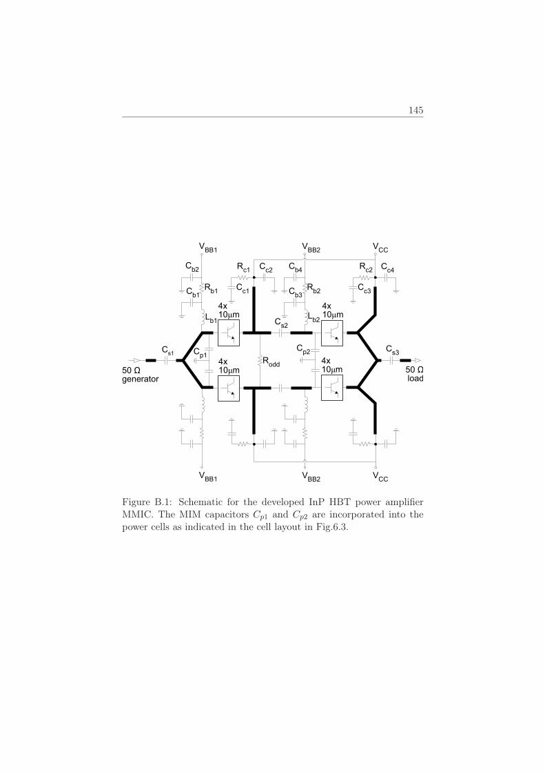
145
Cs2
Cs3
VBB2
VCC
50load
Cs1
4x
10 m
Cp1
Lb2
Rb2
Rodd
Rc1
Cc2
4x
10 mLb1
Rb1C
b1
Cb2
VBB1
50generator
4x
10 m4x
10 m
Cp2
Cc1 C
b3
Cb4
Rc2 C
c4
Cc3
VBB2
VCC
VBB1
Figure B.1: Schematic for the developed InP HBT power amplifierMMIC. The MIM capacitors Cp1 and Cp2 are incorporated into thepower cells as indicated in the cell layout in Fig.6.3.

Appendix C
Derivations of the OscillatorEquations
This appendix explains the derivation of the equations for the simpli-fied small-signal oscillator model from the Fig.7.7 (lower plot). Thediagram is repeated in the Fig.C.1.
gmV
be Lr
Vc
gm1
Vbe1
Vb1 V
e1R
LR
b1
Cbc1 G
bmi
Feedback-buffer
Cbmi
Ybmo C
L
Cbc,eq
+Cr
+V
be-
+V’
be-
Figure C.1: Simplified equivalent diagram of the buffered cross-coupled oscillator. A copy of the Fig.7.7 (lower plot).
All approximations in the following analysis were validated in fre-quency range 30-70GHz, and 2-5mA bias currents Ifb and Icr of thefeedback buffer and core transistors, respectively. Note that Icr in thesimplified small-signal model represents the current of three differentdevices, core, coupling and output device, but in the real circuit, onlythe core device current is varied. To reduce the size of the expressionsin the following derivations, a frequency dependent subfunction F isintroduced,
F =1
1 + (ωCLRL)2. (C.1)
146

147
Here, the product CLRL is the time constant of the parasiticsloading the feedback-buffer. The cut-off frequency 1/(2πCLRL) rangesfrom 24 to 37 GHz in the given bias-current range of the loading-transistors.
Voltage transfer function Ve1/Vb1 of the buffered oscillator small-signal equivalent circuit from the Fig.C.1 is found to be
A =Ve1
Vb1=
gm1 + sCbe1(gm1 + 1
RL− F
RL
)+ s (Cbe1 + CLF )
(C.2)
' gm1 + sCbe1(gm1 + 1
RL
)+ s
(Cbe1 + CL
11+(ωCLRL)2
) (C.3)
The F/RL is neglected in the eq. C.3 since it is at least 6.7 timessmaller as compared to the sum of the other real terms. The expressionis increasingly valid as the frequency goes beyond 30 GHz, since theF-term disappears.
Miller transformation of the Cbe1 to the input side of the feedback-buffer provides the equivalent input admittance
Ybmi = sCbe1(1−A) (C.4)
= sCbe1
(gm1
RL+ 1
R2L
)+ ω2CLF (Cbe1 + CLF ) + s
(gm1CLF − Cbe1
RL
)
(gm1 + 1
RL
)2+ ω2 (Cbe1 + CLF )2
(C.5)
' ω2Cbe1
Cbe1RL
− gm1CL
1+(ωCLRL)2
(1 + gm1RL)+ sCbe1
11 + gm1RL
(C.6)
= Gbmi + sCbmi. (C.7)
Two simplifications have been made in eq.(C.5). Namely, the ω2-terms in numerator and denominator have been neglected since theyare more than order of magnitude smaller than the two other realterms in the numerator and the denominator, respectively. Ybmi com-ponent will affect behavior of the resonator in the Fig.C.1.

148 Appendix C. Derivations of the Oscillator Equations
Similarly, an equivalent impedance
Ybmo = sCbe11
1−A(C.8)
= sCbe1
−1RL
− sCLF
gm1 + sCbe1(C.9)
= sCbe1
−
ω2Cbe1CLF − gm1
RL+ s
(Cbe1RL
− gm1CLF)
(ωCbe1)2 + g2
m1
(C.10)
' ω2Cbe1
gm1
(CLF − Cbe1
gm1RL
)− s
Cbe1
gm1RL(C.11)
can be connected to the output side. It was shown that the two ω2-terms in eq.(C.10) are more than order of magnitude smaller as com-pared to the dominant real terms in the numerator and denominator,respectively. Therefore they have been omitted in the derivation ofthe eq.(C.11).
The two admittances of the Miller equivalent circuit from theFig.C.1 are now derived. Next step towards determination of the os-cillation frequency is to find the voltage transfer function V
′be/Vb1. It
is given by
V′be
Vb1=
gm1
(sCLRL + 1)(Ybmo + 1
RL+ gm1
)− 1
RL
(C.12)
' gm1
(sCLRL + 1)(−s Cbe1
gm1RL+ 1
RL+ gm1
)− 1
RL
. (C.13)
where the approximation is justified by the fact that the real part ofthe Ybmo from the equations (C.8)-(C.11) is two orders of magnitudesmaller as compared to 1/RL+gm1. Separation of the Ybmo in eq.(C.11)into real and imaginary part has greatly simplified the subsequentderivations, since its rather large expression is reduced to a singleimaginary term. Expression for the angle of the transfer functionfrom eq.(C.13) becomes relatively simple,

149
∠(
V′be
Vb1
)= − arctan
(1 + gm1RL − Cbe1
CLgm1RL
ωCbe1gm1
+ gm1
ωCL
)(C.14)
' − arctan
(1 + gm1RLωCbe1gm1
+ gm1
ωCL
). (C.15)
The neglected last term of the numerator of eq.(C.11) is more than 20times smaller than (1 + RLgm1) in above-mentioned frequency rangeand bias range. Figure C.2 compares the calculated phase of eq.(C.15)with with an exact phase, calculated without any simplifications madein this chapter. Despite of the simplifications, an excellent agreementhas been achieved in the expected bias range, 2-5 mA and frequencyrange 30-70 GHz. At lower bias of the feedback buffer, Ifb < 2mA,the equation C.15 is not longer valid in the higher frequency range asindicated in the rightmost plot.
0 50 100−80
−60
−40
−20
Frequency [GHz]
Pha
se(V
be´/
Vb1
) [d
eg]
Ifb
=2mA, Icr
=5mA
0 50 100−80
−60
−40
−20
0
Frequency [GHz]
Pha
se(V
be´/
Vb1
) [d
eg]
Ifb
=5mA, Icr
=2mA
0 50 100−80
−60
−40
−20
0
Frequency [GHz]
Pha
se(V
be´/
Vb1
) [d
eg]
Ifb
=1mA, Icr
=5mA
Figure C.2: Exact phase (-) and phase approximated by eq.(C.15) (··)at three different combinations of the bias currents.

Bibliography
[1] T. Palacios, A. Chakraborty, S. Rajan, C. Poblenz, S. Keller, S. Den-Baars, J. Speck, and U. Mishra, “High-power algan/gan hemts forka-band applications,” IEEE Electron Device Letters, vol. 26, no. 11,pp. 781–783.
[2] J. Das, J. Derluyn, A. Lorenz, H. Oprins, D. Xiao, W. De Raedt,K. Cheng, M. Leys, S. Degroote, M. Germain, and G. Borghs, “Gantechnology on high-resistivity si-substrates for high-power-amplifiers,”ESA, Microwave Technology and Techniques Workshop, 2008.
[3] L. Shen, T. Palacios, C. Poblenz, A. Corrion, A. Chakraborty,N. Fichtenbaum, S. Keller, S. Denbaars, J. Speck, and U. Mishra,“Unpassivated high power deeply recessed gan hemts with fluorine-plasma surface treatment,” IEEE Electron Device Letters, vol. 27,no. 4, pp. 214–216, 2006.
[4] R. Lossy, N. Chaturvedi, P. Heymann, K. Köhler, S. Müller, andJ. Würfl, “Algan/gan hemts on silicon carbide substrates for microwavepower operation,” GaAs ManTech, 2003.
[5] V. Krozer. Private communication, 2008.
[6] J. Wiltse, “Corrections to published curves for atmospheric attenuationin the 10 to 1000 ghz region,” IEEE Antennas and Propagation SocietyInternational Symposium 1997. Digest, vol. 4, pp. 2580–2583 vol.4,1997.
[7] G. Weibel and H. Dressel, “Propagation studies in millimeter-wave linksystems,” Proceedings of the IEEE, vol. 55, no. 4, pp. 497–513, 1967.
[8] C. Karnfelt, P. Hallbjorner, H. Zirath, and A. Alping, “High gain activemicrostrip antenna for 60-ghz wlan/wpan applications,” IEEE Trans-actions on Microwave Theory and Techniques, vol. 54, no. 6, pp. 2593–2603, 2006.
[9] G. Boeck, V. Subramanian, W. Keusgen, and V. H. Do, “60 ghzsige hbt chip set for high speed wireless communication systems,”EuMC/EuMIC Workshop WTH-11: Modelling, Circuit Design andMeasurement Techniques for Millimeter Wave Systems, 2006.
[10] V. Dyadyuk, O. Sevimli, J. Bunton, J. Pathikulangara, and L. Stokes,“A 6 gbps millimetre wave wireless link with 2.4 bit/hz spectral effi-ciency,” 2007 IEEE/MTT-S IMS, pp. 471–474, 2007.
150

Bibliography 151
[11] T. K. Johansen. Private communication, 2006.
[12] K. Lee, J. Edie, R. Krueger, J. Weber, T. Brott, and W. Craig, “A lowprofile x-band active phased array for submarine satellite communi-cations,” Proceedings 2000 IEEE International Conference on PhasedArray Systems and Technology, pp. 231–234, 2000.
[13] Y.-B. Jung, S.-Y. Eom, S.-I. Jeon, C.-J. Kim, and S.-O. Park, “T/rxchannel design of x-band shipboard apaa system for mobile communi-cations via satellite,” European Microwave Conference, 2003, pp. 527–530, 2003.
[14] R. Tahim, J. Foshee, and K. Chang, “Multi-band phased array anten-nas for air-platforms,” IEEE Antennas and Propagation Society, AP-SInternational Symposium (Digest), vol. 4, pp. 204–207, 2002.
[15] J. C. Chen, L. Cooper, D. Taggart, N. S. Wagner, R. Kumar,T. Nguyen, J. Yoh, G. Leon, and G. W. Goo, “Performance ofmpsk and 16qam in the satellite communication environment,” IEEEAerospace Conference Proceedings, vol. 2, pp. 1383–1390, 2004.
[16] A. Ghorbani and M. Sheikhan, “The effect of solid state power am-plifiers (sspas) nonlinearities on mpsk and m-qam signal transmis-sion,” Sixth International Conference on Digital Processing of Signalsin Communications, pp. 193–197, 1991.
[17] H. Takasu, F. Sadaki, M. Kawano, and S. Kamihashi, “Ka-band lowloss and high power handling gaas pin diode mmic phase shifter forreflected-type phased array systems,” 1999 IEEE MTT-S IMS Digest,vol. 2, pp. 467–470 vol.2, 1999.
[18] International Manufacturing Services, Application notes: Thick FilmTwo Way Wilkinson Power Divider - (www.ims-resistors.com).
[19] S. Piotrowicz, E. Chartier, J. Jacquet, D. Floriot, J. Obregon,P. Dueme, J. Delaire, and Y. Mancuso, “Ultra compact x-bandgainp/gaas hbt mmic amplifiers : 11w, 42% of pae on 13mm and 8.7w,38% of pae on 9mm,” IEEE MTT-S IMS Digest, pp. 1867–1870, 2006.
[20] Z. Ouarch, “X-band gainp hbt 10 w high power amplifier including on-chip bias control circuit,” IEEE MTT-S IMS Digest, vol. 2, pp. 855–858, 2003.
[21] F. Lenk, H. Klockenhoff, P. Kurpas, A. Maabdorf, H. Wurfl, andW. Heinrich, “A 3.2 w coplanar single-device x-band amplifier withgaas hbt,” 2005 13th European Gallium Arsenide and other CompoundSemiconductors Application Symposium, pp. 49–52, 2006.
[22] K. Riepe, H. Leier, U. Seiler, A. Marten, and H. Sledzik, “High-efficiency gainp/gaas hbt mmic power amplifier with up to 9 w outputpower at 10 ghz,” IEEE Microwave and Guided Wave Letters, vol. 6,no. 1, pp. 22–24, 1996.
[23] M. Khatibzadeh, B. Bayraktaroglu, and T. Kim, “12 w monolithicx-band hbt power amplifier,” IEEE, Microwave and Millimeter-WaveMonolithic Circuits Symposium, Digest of Papers, pp. 47–50, 1992.

152 Bibliography
[24] J. Komiak and L. Yang, “5 watt high efficiency wideband 7 to 11 ghzhbt mmic power amplifier,” IEEE, Microwave and Millimeter-WaveMonolithic Circuits Symposium, Digest of Papers, pp. 17–20, 1995.
[25] C.-K. Chu, H.-K. Huang, H.-Z. Liu, C.-H. Lin, C.-H. Chang, C.-L. Wu,C.-S. Chang, and Y.-H. Wang, “A 9.1-10.7 ghz 10 w, 40 db gain four-stage phemt mmic power amplifier,” IEEE Microwave and WirelessComponents Letters, vol. 17, no. 2, p. 151, 2007.
[26] A. Bessemoulin, M. Quay, S. Ramberger, and M. Schlechtweg, “A 4-watt x-band compact coplanar high power amplifier mmic with 18-dbgain and 25-% pae,” Gallium Arsenide Integrated Circuit (GaAs IC)Symposium, 2002. 24th Annual Technical Digest, pp. 189–192, 2002.
[27] C. Chu, H. Huang, H. Liu, R. Chiu, C. Lin, C. Wang, Y. Wang,C. Hsu, W. Wu, C. Wu, and C. Chang, “A fully matched 8w x-bandphemt mmic high power amplifier,” IEEE, CSIC, Technical Digest,pp. 137–140, 2004.
[28] P. Colantonio, F. Giannini, R. Giofre, E. Limiti, C. Lanzieri, and S. La-vanga, “A two stage high frequency class f power amplifier,” INMMIC2007 - Proceedings, pp. 187–190 and 4062294, 2007.
[29] M. Van Heijningen, A. De Boer, J. Hoogland, M. Van Wanum,A. De Hek, F. Van Vliet, and H. Brouzes, “Multi function and highpower amplifier chipset for x-band phased array frontends,” EuMIC2006 - Proceedings, pp. 237–240, 2007.
[30] S. Chu, A. Platzker, M. Borkowski, R. Mallavarpu, M. Snow,A. Bowlby, D. Teeter, T. Kazior, and K. Alavi, “A 7.4 to 8.4 ghz highefficiency phemt three-stage power amplifier,” IEEE 2000 MTT-S IMSDigest, vol. 2, pp. 947–950, 2000.
[31] H. Klockenhoff, R. Behtash, J. Wurfl, W. Heinrich, and G. Trankle,“A compact 16 watt x-band gan-mmic power amplifier,” IEEE MTT-SIMS Digest, pp. 1846–1849, 2006.
[32] F. van Raay, M. Dammann, M. Mikulla, M. Schlechtweg, G. Weimann,R. Quay, R. Kiefer, F. Benkhelifa, B. Raynor, W. Pletschen, M. Kuri,H. Massler, and S. Muller, “A coplanar x-band algan/gan power ampli-fier mmic on s.i. sic substrate,” IEEE Microwave and Wireless Com-ponents Letters, vol. 15, no. 7, pp. 460–462, 2005.
[33] P. Schuh, R. Kiefer, R. Leberer, H. Sledzik, M. Oppermann,B. Adelseck, H. Brugger, R. Behtash, H. Leier, and R. Quay, “20wgan hpas for next generation x-band t/r-modules,” IEEE MTT-S IMSDigest, pp. 726–729, 2006.
[34] S. Sheppard, R. Smith, W. Pribble, Z. Ring, T. Smith, S. Allen,J. Milligan, and J. Palmour, “High power hybrid and mmic ampli-fiers using wide-bandgap semiconductor devices on semi-insulating sicsubstrates,” 60th DRC. Conference Digest, pp. 175–178, 2002.
[35] F. van Raay, R. Quay, R. Kiefer, W. Bronner, M. Seelmann-Eggebert,M. Schlechtweg, M. Mikulla, and G. Weimann, “X-band high-powermicrostrip algan/gan hemt amplifier mmics,” IEEE MTT-S IMS Di-gest, pp. 1368–1371, 2006.

Bibliography 153
[36] D. Fanning, L. Witkowski, C. Lee, D. Dumka, H. Tserng, P. Saunier,W. Gaiewski, E. Piner, K. Linthicum, and J. J.W., “25 w x-band ganon si mmic,” GaAs Man.Tech. Digest, 2005.
[37] D. Johnson and S. Raman, “A packaged sige x2 sub-harmonic mixerfor u-nii band applications,” Proceedings of the IEEE Bipolar/BiCMOSCircuits and Technology Meeting, pp. 159–162, 2001.
[38] R. Kodkani and L. Larson, “An integrated 50-ghz sige sub-harmonicmixer/downconverter with a quadrature ring vco,” 2007 Topical Meet-ing on Silicon Monolithic Integrated Circuits in RF Systems, p. 4 pp.,2006.
[39] K. Nimmagadda and G. Rebeiz, “A 1.9 ghz double-balanced subhar-monic mixer for direct conversion receivers,” 2001 IEEE RFIC Sym-posium, pp. 253–256, 2001.
[40] Hittite Microwave Corporation, Application notes: SUBHARMONICvs. FUNDAMENTAL MIXERS FOR HIGH CAPACITY MILLIME-TERWAVE RADIOS - (www.hittite.com).
[41] B. Razavi, RF Microelectronics. Prentice Hall PTR, 1998.
[42] J. Craninckx, V. Gravot, and S. Donnay, “A harmonic quadrature logenerator using a 90o delay-locked loop,” ESSCIRC 2004 - Proceedings,pp. 127–130, 2004.
[43] K.-J. Koh, M.-Y. Park, C.-S. Kim, and H.-K. Yu, “Subharmonicallypumped cmos frequency conversion (up and down) circuits for 2-ghzwcdma direct-conversion transceiver,” IEEE Journal of Solid-StateCircuits, vol. 39, no. 6, pp. 871–884, 2004.
[44] D. Leeson, “A simple model of feedback oscillator noise spectrum,”Proceedings of the IEEE, vol. 54, no. 2, pp. 329–330, 1966.
[45] F. Ellinger and H. Jackel, “38-43 ghz quadrature vco on 90 nm vlsi cmoswith feedback frequency tuning,” IEEE MTT-S IMS Digest, vol. 2005,pp. 1701–1703 and 1517042, 2005.
[46] M. Usama and T. A. Kwasniewski, “A 40 ghz quadrature lc vco andfrequency divider in 90-nm cmos technology,” Proceedings - IEEE In-ternational Symposium on Circuits and Systems, pp. 3047–3050 and4253321, 2007.
[47] M. Sanduleanu and E. Stikvoort, “Highly linear, varactor-less, 24ghziq oscillator,” RFIC) Symposium, Digest of Papers, pp. 577–580, 2005.
[48] W. Chan, H. Veenstra, and J. Long, “A 32ghz quadrature lc-vco in0.25ţm sige bicmos technology,” Digest of Technical Papers - IEEEInternational Solid-State Circuits Conference, vol. 48, pp. 448–449 and29.5, 2005.
[49] S. Hackl, J. Bock, G. Ritzberger, M. Wurzer, and A. L. Scholtz, “A 28-ghz monolithic integrated quadrature oscillator in sige bipolar technol-ogy,” IEEE Journal of Solid-State Circuits, vol. 38, no. 1, pp. 135–137,2003.

154 Bibliography
[50] E. Johnson, “Physical limitations on frequency and power parametersof transistors,” RCA Review, vol. 26, no. 2, pp. 163–177, 1965.
[51] M. Micovic, A. Kurdoghlian, P. Hashimoto, M. Hu, M. Antcliffe,P. Willadsen, W. Wong, R. Bowen, I. Milosavljevic, A. Schmitz,M. Wetzel, and D. Chow, “Gan hfet for w-band power applications,”International Electron Devices Meeting, pp. 1–3, 2006.
[52] A. Komijani and A. Hajimiri, “A wideband 77ghz, 17.5dbm poweramplifier in silicon,” IEEE Proceedings, Custom Integrated CircuitsConference, pp. 571–574, 2005.
[53] T. Ishibashi, “Nonequilibrium electron transport in hbts,” IEEE Trans-actions on Electron Devices, vol. 48, no. 11, p. 2595, 2001.
[54] H. Wang, R. Lai, M. Biedenbender, G. Dow, and B. Allen, “Novel w-band monolithic push-pull power amplifiers,” IEEE Journal of Solid-State Circuits, vol. 30, no. 10, pp. 1055–1061, 1995.
[55] R. Lai, R. Grundbacher, M. Barsky, A. Oki, M. Siddiqui, B. Pitman,R. Katz, P. Tran, L. Callejo, and D. Streit, “Extremely high p1db mmicamplifiers for ka-band applications,” 2001 IEEE GaAs IC Symposium- Technical Digest, pp. 115–17, 2001.
[56] J. Komiak, W. Kong, and K. Nichols, “High efficiency wideband 6 to 18ghz phemt power amplifier mmic,” 2002 IEEE MTT-S InternationalMicrowave Symposium Digest (Cat. No.02CH37278), pp. 905–7 vol.2,2002.
[57] S.-W. Chen, P. Smith, S.-M. Liu, W. Kopp, and T. Rogers, “A 60-ghz high efficiency monolithic power amplifier using 0.1-µm phemt’s,”IEEE Microwave and Guided Wave Letters, vol. 5, no. 6, pp. 201–203,1995.
[58] F. Y. Colomb and A. Platzker, “A 3-watt q-band gaas phemt poweramplifier mmic for high temperature operation,” IEEE MTT-S IMSDigest, pp. 897–900, 2006.
[59] P. M. Smith, S.-M. J. Liu, M.-Y. Kao, P. Ho, S. C. Wang, K. H. G.Duh, S. T. Fu, and P. C. Chao, “W-band high efficiency inp-basedpower hemt with 600 ghz fmax,” IEEE Microwave and Guided WaveLetters, vol. 5, no. 7, pp. 230–232, 1995.
[60] L. Samoska, A. Peralta, M. Hu, M. Micovic, and A. Schmitz, “A 20mw, 150 ghz inp hemt mmic power amplifier module,” Microwave andWireless Components Letters, IEEE, vol. 14, no. 2, pp. 56–58, 2004.
[61] S. Liu, O. Tang, W. Kong, K. Nichols, J. Heaton, and P. Chao, “Highefficiency monolithic inp hemt v-band power amplifier,” GaAs IC Sym-posium, 1999, pp. 145–147, 1999.
[62] P. Huang, R. Lai, R. Grundbacher, and B. Gorospe, “A 20-mw g-band monolithic driver amplifier using 0.07-µm inp hemt,” IEEE 2006MTT-S IMS Digest, pp. 806–809, 2006.
Bibliography 155
[63] W. Deal, X. Mei, V. Radisic, M. Lange, W. Yoshida, L. Po-hsin,J. Uyeda, M. Barsky, A. Fung, T. Gaier, and R. Lai, “Developmentof sub-millimeter-wave power amplifiers,” IEEE Transactions on Mi-crowave Theory and Techniques, vol. 55, no. 122, pp. 2719–2726.
[64] K. Herrick, S. Lardizabal, P. Marsh, and C. Whelan, “95 ghz metamor-phic hemt power amplifiers on gaas,” 2003 IEEE MTT-S IMS Digest,vol. 1, pp. 137–140 vol.1, 2003.
[65] P. Smith, D. Dugas, K. Chu, K. Nichols, K. Duh, J. Fisher,L. Mt Pleasant, D. Xu, L. Gunter, A. Vera, R. Lender, and D. Meharry,“Progress in gaas metamorphic hemt technology for microwave appli-cations,” ESSDERC 2003 - Proceedings, pp. 21–24, 2003.
[66] D. M. Kang, J. Y. Hong, J. Y. Shim, J.-H. Lee, H.-S. Yoon, and K. H.Lee, “A 77 ghz mhemt mmic chip set for automotive radar systems,”ETRI Journal, vol. 27, no. 2, pp. 133–139, 2005.
[67] M. Salib, A. Gupta, F. Ali, and D. Dawson, “1.8-W, 6-18-GHz HBTMMIC power amplifier with 10-dB gain and 37% peak power-addedefficiency,” IEEE Microwave and Guided Wave Letters, vol. 3, no. 9,pp. 325–326, 1993.
[68] S. Tanaka, S. Yamanouchi, Y. Amamiya, T. Niwa, K. Hosoya, H. Shi-mawaki, and K. Honjo, “A ka-band hbt mmic power amplifier,” 2000IEEE MTT-S IMS Digest, pp. 553–6 vol.1, 2000.
[69] K. Kobayashi, A. Oki, L.-W. Yang, A. Gutierrez-Aitken, P. Chin,D. Sawdai, W. Okamura, J. Lester, E. Kaneshiro, P. Grossman,K. Sato, T. Block, H. Yen, and D. Streit, “A 0.5 watt-40% pae inpdouble heterojunction bipolar transistor k-band mmic power ampli-fier,” International Conference on Indium Phosphide and Related Ma-terials - Proceedings, pp. 250–253, 2000.
[70] V. Paidi, Z. Griffith, Y. Wei, M. Dahlstrom, M. Urteaga,N. Parthasarathy, M. Seo, L. Samoska, A. Fung, and M. Rodwell, “G-band (140-220 ghz) and w-band (75-110 ghz) inp dhbt medium poweramplifiers,” IEEE Transactions on Microwave Theory and Techniques,vol. 53, no. 2, pp. 598–605, 2005.
[71] G. Ellis, A. Kurdoghlian, R. Bowen, M. Wetzel, and M. Delaney, “W-band inp dhbt mmic power amplifiers,” 2004 IEEE MTT-S IMS Di-gest, vol. 1, pp. 231–234, 2004.
[72] T. Quach, W. Okamura, A. Gutierrez-Aitken, T. Jenkins,E. Kaneshiro, L. Kehias, A. Oki, D. Sawdai, P. Watson, R. Welch,R. Worley, and H. Yen, “Ultra-efficient x-band and linear-efficient ka-band power amplifiers using indium phosphide double heterojunctionbipolar transistors,” Conference Proceedings - International Confer-ence on Indium Phosphide and Related Materials, pp. 501–504, 2001.
[73] V. Paidi, Z. Griffith, Y. Wei, M. Dahlstrom, N. Parthasarathy,M. Urteaga, M. Rodwell, A. Fung, and L. Samoska, “Common baseamplifier with 7-db gain at 176 ghz in inp mesa dhbt technology,”2004 IEEE RFIC Symposium - Digest of Papers, pp. 189–192, 2004.

156 Bibliography
[74] L. Yang, K. Kobayashi, D. Steit, A. Oki, H. Yen, P. Grossman,T. Block, L. Tran, A. Gutierrez-Aitken, L. Callejo, J. Macek, andS. Maas, “High linearity k-band inp hbt power amplifier mmic with62.8% pae at 21 ghz,” IEEE 1999 GaAs IC Symposium - TechnicalDigest, pp. 73–76, 1999.
[75] J. Hacker, W. Ha, C. Hillman, M. Urteaga, R. Pierson, and B. Brar,“Compact inp hbt power amplifiers using integrated thick bcb di-electrics,” 2007 IEEE MTT-S IMS, pp. 805–808, 2007.
[76] P. Huang, E. Lin, R. Lai, M. Biedenbender, T. Huang, H. Wang,C. Geiger, T. Block, and P. Liu, “A 94 ghz monolithic high outputpower amplifier,” 1997 IEEE MTT-S IMS Digest, no. vol.3, pp. 1175–8, 1997.
[77] O. Tang, K. Duh, S. Liu, P. Smith, W. Kopp, T. Rogers, andD. Pritchard, “Design of high-power, high-efficiency 60-ghz mmics us-ing an improved nonlinear phemt model,” IEEE Journal of Solid-StateCircuits, vol. 32, no. 9, pp. 1326–1333, 1997.
[78] D. Ingram, Y. Chen, J. Kraus, B. Brunner, B. Allen, H. Yen, andK. Lau, “A 427 mw, 20% compact w-band inp hemt mmic power am-plifier,” 1999 IEEE RFIC Symposium, pp. 95–98, 1999.
[79] M. Yu, M. Matloubian, P. Petre, L. Hamilton, R. Bowen, M. Lui,H. Sun, C. Ngo, P. Janke, D. Baker, and R. Robertson, “W-band inp-based hemt mmic power amplifiers using finite-ground cpw design,”Technical Digest - GaAs IC Symposium, pp. 37–40, 1998.
[80] Y. C. C. et al., “A single chip 1-w inp hemt v-band module,” GaAs ICSymposium, 1999. 21st Annual, pp. 149–152, 1999.
[81] A. Tessmann, A. Leuther, C. Schwoerer, and H. Massler, “Metamor-phic 94 ghz power amplifier mmics,” 2005 IEEE MTT-S IMS Digest,p. 4 pp., 2005.
[82] Y. Wei, M. Urteaga, Z. Griffith, D. Scott, S. Xie, V. Paidi,N. Parthasarathy, and M. Rodwell, “75 ghz 80 mw inp dhbt poweramplifier,” IEEE MTT-S International Microwave Symposium Digest,vol. 2, pp. 919–921, 2003.
[83] T. O’Sullivan, M. Le, P. Partyka, R. Milano, and P. Asbeck, “Design ofa 70 ghz power amplifier using a digital inp hbt process,” 2007 IEEEBipolar/BiCMOS Circuits and Technology Meeting, pp. 214–217, 2007.
[84] U. R. Pfeiffer, S. K. Reynolds, and B. A. Floyd, “A 77 ghz sige poweramplifier for potential applications in automotive radar systems,” Di-gest of Papers - 2004 IEEE RFIC Symposium, pp. 91–94, 2004.
[85] U. Pfeiffer, “A 20dbm fully-integrated 60ghz sige power amplifier withautomatic level control,” Proceedings - ESSCIRC (IEEE Cat. No.06EX1347), pp. 356–9, 2006.
[86] E. Afshari, H. Bhat, X. Li, and A. Hajimiri, “An electrical funnel:a broadband signal combining method,” Solid-State Circuits, IEEEInternational Conference Digest of Technical Papers, p. 10 pp., 2006.

Bibliography 157
[87] V.-H. Do, V. Subramanian, W. Keusgen, and G. Boeck, “A 60 ghzsige-hbt power amplifier with 20% pae at 15 dbm output power,” IEEEMicrowave and Wireless Components Letters, vol. 18, no. 3, pp. 209–211, 2008.
[88] U. R. Pfeiffer and D. Goren, “A 23-dbm 60-ghz distributed activetransformer in a silicon process technology,” IEEE Transactions onMicrowave Theory and Techniques, vol. 55, no. 5, pp. 857–865, 2007.
[89] M. Rodwell, M. Urteaga, Y. Betser, T. Mathew, P. Krishnan, D. Scott,S. Jaganathan, D. Mensa, J. Guthrie, R. Pullela, Q. Lee, B. Agarwal,U. Bhattacharya, and S. Long, “Scaling of ingaas/inalas hbts for highspeed mixed-signal and mm-wave ics,” International Journal of HighSpeed Electronics and Systems, vol. 11, no. 1, pp. 159–215, 2001.
[90] F. Colomb and A. Platzker, “2 and 4 watt ka-band gaas phemt poweramplifier mmics,” 2003 IEEE MTT-S IMS Digest, pp. 843–846 vol.2,2003.
[91] R. Kasody, G. Dow, A. Sharma, M. Aust, D. Yamauchi, R. Lai,M. Biedenbender, K. Tan, and B. Allen, “A high efficiency v-bandmonolithic hemt power amplifier,” IEEE Microwave and Guided WaveLetters, vol. 4, no. 9, pp. 303–304, 1994.
[92] C. Lin, H. Liu, C. Chu, H. Huang, Y. Wang, C. Liu, C. Chang, C. Wu,and C. Chang, “A fully matched ku-band 9w phemt mmic high poweramplifier,” Compound Semiconductor Integrated Circuit Symposium,2006 IEEE, pp. 165–168, 2006.
[93] L. Samoska and Y. C. Leong, “65-145 ghz inp mmic hemt mediumpower amplifiers,” Microwave Symposium Digest, 2001 IEEE MTT-SInternational, vol. 3, pp. 1805–1808 vol.3, 2001.
[94] F. Lam, M. Matloubian, A. Igawa, C. Chou, A. Kurdoghlian, C. Ngo,L. Jelloian, A. Brown, M. Thompson, and L. Larson, “44-ghz high-efficiency inp-hemt mmic power amplifier,” IEEE Microwave andGuided Wave Letters, vol. 4, no. 8, pp. 277–278, 1994.
[95] P. J. Bartusiak, T. Henderson, T. Kim, and B. Bayraktaroglu, “High-efficiency ku-band hbt mmic power amplifier,” IEEE Electron DeviceLetters, vol. 13, no. 11, pp. 584–586, 1992.
[96] Y. Wei, K. Sundararajan, M. Urteaga, Z. Griffith, D. Scott, V. Paidi,N. Parthasarathy, and M. Rodwell, “40 ghz mmic power amplifier ininp dhbt technology,” Proceedings IEEE Lester Eastman Conferenceon High Performance Devices, pp. 352–357, 2002.
[97] A. Schott, H. Kuhnert, F. Lenk, J. Hilsenbeck, J. Wurfl, and W. Hein-rich, “38 ghz push-push gaas-hbt mmic oscillator,” 2002 IEEE MTT-SIMS Digest, no. vol.2, pp. 839–42 vol.2, 2002.
[98] F. Lenk, M. Schott, J. Hilsenbeck, and W. Heinrich, “Low phase-noisegaas-hbt monolithic w-band oscillator,” 2004 EuMC, vol. 2, pp. 897–900.
[99] M. Bao, Y. Li, and H. Jacobsson, “A 25-ghz ultra-low phase noiseingap/gaas hbt vco,” IEEE Microwave and Wireless Components Let-ters, vol. 15, no. 11, pp. 751–753, 2005.

158 Bibliography
[100] A. Inoue, H. Amasuga, S. Watanabe, S. Goto, and T. Oku, “Mmictechnologies for mw and mmw applications,” 2007 IEEE InternationalWorkshop on Radio-Frequency Integration Technology, pp. 232–235,2007.
[101] K. Uchida, I. Aoki, H. Matsuura, T. Yakihara, S. Kobayashi, S. Oka,T. Fujita, and A. Miura, “104 and 134 ghz ingap/ingaas hbt oscil-lators,” IEEE GaAs IC Symposium - Technical Digest, pp. 237–240,1999.
[102] T. Kashiwa, T. Ishida, T. Katoh, H. Kurusu, H. Hoshi, and Y. Mit-sui, “V-band high-power low phase-noise monolithic oscillators andinvestigation of low phase-noise performance high drain bias,” IEEETransactions on Microwave Theory and Techniques, vol. 46, no. 102,pp. 1559–1565, 1998.
[103] S. Kudszus, T. Berceli, A. Tessmann, M. Neumann, and W. Haydl,“W-band hemt-oscillator mmics using subharmonic injection locking,”IEEE Transactions on Microwave Theory and Techniques, vol. 48,no. 12, pp. 2526–2532, 2000.
[104] J. Lin, Y. Chen, D. Humphrey, R. Hamm, R. Malik, A. Tate, R. Kopf,and R. Ryan, “Ka-band monolithic ingaas/inp hbt vco’s in cpw struc-ture,” IEEE Microwave and Guided Wave Letters, vol. 5, no. 11,pp. 379–381, 1995.
[105] Z. Lao, J. Jensen, K. Guinn, and M. Sokolich, “80-ghz differentialvco in inp shbts,” IEEE Microwave and Wireless Components Letters,vol. 14, no. 9, pp. 407–409, 2004.
[106] H. Wang, K. W. Chang, L. T. Tran, J. C. Cowles, T. R. Block, E. W.Lin, G. S. Dow, A. K. Oki, D. C. Streit, and B. R. Allen, “Low phasenoise millimeter-wave frequency sources using inp-based hbt mmictechnology,” IEEE Journal of Solid State Circuits - Institute of Electand Electr Engineers, vol. 31, no. 10, p. 1419, 1996.
[107] K. Kobayashi, A. Oki, L. Tran, J. Cowles, A. Gutierrez-Aitken, F. Ya-mada, T. Block, and D. Streit, “A 108-ghz inp-hbt monolithic push-push vco with low phase noise and wide tuning bandwidth,” IEEEJournal of Solid-State Circuits, vol. 34, no. 9, pp. 1225–1232, 1999.
[108] Y. Baeyens, C. Dorschky, N. Weimann, Q. Lee, R. Kopf, G. Georgiou,J.-P. Mattia, R. Hamm, and Y.-K. Chen, “Compact inp-based hbtvcos with a wide tuning range at w- and d-band,” IEEE Transactionson Microwave Theory and Techniques, vol. 48, no. 12, pp. 2403–2408,2000.
[109] R. Wanner, R. Lachner, and G. Olbrich, “Sige integrated mm-wavepush-push vcos with reduced power consumption,” IEEE RFIC Sym-posium, 2006, p. 4 pp., 2006.
[110] S. Trotta, H. Knapp, K. Aufinger, T. Meister, J. Bock, W. Simburger,and A. Scholtz, “A fundamental vco with integrated output bufferbeyond 120 ghz in sige bipolar technology,” 2007 IEEE/MTT-S IMS,pp. 645–648, 2007.

Bibliography 159
[111] H. Li and H.-M. Rein, “Millimeter-wave vcos with wide tuning rangeand low phase noise, fully integrated in a sige bipolar production tech-nology,” IEEE Journal of Solid-State Circuits, vol. 38, no. 2, pp. 184–191, 2003.
[112] Y. Wachi, T. Nagasaku, and H. Kondoh, “A 28ghz low-phase-noisecmos vco using an amplitude-redistribution technique,” 2008 IEEEInternational Solid-State Circuits Conference - Digest of Technical Pa-pers, pp. 482–630, 2008.
[113] G. Le Grand de Mercey, “A 18ghz rotary traveling wave vco in cmoswith i/q outputs,” ESSCIRC 2004, pp. 489–492, 2003.
[114] J.-C. Chien and L.-H. Lu, “40ghz wide-locking-range regenerative fre-quency divider and low-phase-noise balanced vco in 0.18ţm cmos,”2007 IEEE International Solid-State Circuits Conference, pp. 544–621,2007.
[115] D. Huang, W. Hant, N.-Y. Wang, T. Ku, Q. Gu, R. Wong, and M.-C. Chang, “A 60ghz cmos vco using on-chip resonator with embeddedartificial dielectric for size, loss and noise reduction,” 2006 IEEE Inter-national Solid-State Circuits Conference. Digest of Technical Papers,p. 10 pp., 2006.
[116] C. Cao, E. Seok, and K. K. O, “Millimeter-wave cmos voltage-controlled oscillators,” 2007 IEEE Radio and Wireless Symposium,pp. 185–188, 2007.
[117] M. Yu, R. J. Ward, R. A. Newgard, and M. Urteaga, “A compact 43-ghz monolithic differential vco in 0.5-ţm inp dhbt technology,” IEEEMicrowave and Wireless Components Letters, vol. 16, no. 5, pp. 281–283, 2006.
[118] D. Hadziabdic, “Low voltage, low noise l-band vco design,” Master’sthesis, Technical University of Denmark, DK-2800 Kgs. Lyngby, 2005.
[119] F.-H. Huang, C.-K. Lin, and Y.-J. Chan, “V-band gaas phemt cross-coupled sub-harmonic oscillator,” IEEE Microwave and Wireless Com-ponents Letters, vol. 16, no. 8, pp. 473–475, 2006.
[120] D. M. Pozar, Microwave Engineering. John Wiley & Sons, 2 ed., 1998.
[121] V. Radisic, X. B. Mei, W. R. Deal, W. Yoshida, P. H. Liu, J. Uyeda,M. Barsky, L. Samoska, A. Fung, T. Gaier, and R. Lai, “Demonstra-tion of sub-millimeter wave fundamental oscillators using 35-nm inphemt technology,” IEEE Microwave and Wireless Components Letters,vol. 17, no. 3, pp. 223–225, 2007.
[122] V. Radisic, D. Sawdai, D. Scott, W. Deal, L. Dang, D. Li, J. Chen,A. Fung, L. Samoska, T. Gaier, and R. Lai, “Demonstration of a 311-ghz fundamental oscillator using inp hbt technology,” IEEE Transac-tions on Microwave Theory and Techniques, vol. 55, no. 11, pp. 2329–2335, 2007.
[123] M. Kraemer, Gallium nitride-based microwave high-power heterostruc-ture field-effect transistors : design, technology, and characterization.PhD thesis, Technische Universiteit Eindhoven, 2006.

160 Bibliography
[124] A. Bessemoulin, W. Marsetz, Y. Baeyens, R. Osorio, H. Massler,A. Hulsmann, and M. Schlechtweg, “Design of coplanar power am-plifiers for mm-wave system applications including thermal aspects,”GAAS 2000. Conference Proceedings, p. 4 pp., 2000.
[125] N. Chaturvedi. Private communication, 2008.
[126] F. Giannini, G. Leuzzi, E. Limiti, and L. Scucchia, “Design-orientednon-linear analysis of class-ab power amplifiers,” IEEE MTT-S IMSDigest, pp. 297–300 vol.1, 1993.
[127] H. C. Casey, Device for Integrated Circuits: Silicon and III-V Com-pound Semiconductors. John Wiley & Sons, 1999.
[128] P. Houston, “High-frequency heterojunction bipolar transistor devicedesign and technology,” Electronics and Communication EngineeringJournal, vol. 12, no. 5, pp. 220–228, 2000.
[129] H. Kroemer, “Heterostructure bipolar transistors: what should webuild?,” Journal of Vacuum Science and Technology B (Microelectron-ics Processing and Phenomena), vol. 1, no. 2, pp. 126–30, 1983.
[130] D. Harame, J. Comfort, J. Cressler, E. Crabbe, J.-C. Sun, B. Mey-erson, and T. Tice, “Si/sige epitaxial-base transistors. i. materials,physics, and circuits,” IEEE Transactions on Electron Devices, vol. 42,no. 3, pp. 455–468, 1995.
[131] J. D. Cressler and G. Niu, Silicon-Germanium Heterojunction BipolarTransistors. Artech House, 2003.
[132] J. Kirk, C.T., “A theory of transistor cutoff frequency (ft) falloff athigh current densities,” IEEE Transactions on Electron Devices, vol. 9,no. 2, pp. 164–174, 1962.
[133] S. Blayac, M. Riet, J. Benchimol, P. Berdaguer, N. Kauffman,J. Godin, and A. Scavennec, “Lateral design of inp/ingaas dhbts for 40gbit/s ics,” Conference Proceedings. International Conference on In-dium Phosphide and Related Materials (Cat. No.00CH37107), pp. 481–484, 2000.
[134] S. Blayac, M. Riet, J. Benchimol, F. Alexandre, P. Berdaguer,M. Kahn, A. Pinquier, E. Dutisseuil, J. Moulu, A. Kasbari, A. Kon-czykowska, and J. Godin, “Msi inp/ingaas dhbt technology: beyond 40gbit/s circuits,” Conference Proceedings. 14th Indium Phosphide andRelated Materials Conference (Cat. No.02CH37307), pp. 51–54, 2002.
[135] J. Godin, M. Riet, P. Berdaguer, V. Nodjiadjim, A. Konczykowska,and A. Scavennec, “Inp dhbt technology development for high bi-trate mixed-signal ic fabrication,” International Conference on IndiumPhosphide and Related Materials Conference Proceedings (IEEE Cat.No.06CH37737C), pp. 258–61, 2006.
[136] J. Godin, P. Andre, J. Benchimol, P. Berdaguer, S. Blayac, J. Burie,P. Desrousseaux, A. Duchenois, N. Kauffmann, A. Konczykowska, andM. Riet, “40 gbit/s optical communications: Inp dhbt technology, cir-cuits and system experiments,” Technical Digest - GaAs IC Symposium(Gallium Arsenide Integrated Circuit), pp. 185–188, 1999.

Bibliography 161
[137] A. Konczykowska, F. Jorge, M. Riet, J. Moulu, and J. Godin, “50 gb/sdff and decision circuits in inp dhbt technology for etdm systems,”13th European Gallium Arsenide and other Compound SemiconductorsApplication Symposium, pp. 605–7, 2006.
[138] J. Godin, V. Nodjiadjim, M. Riet, P. Berdaguer, O. Drisse, E. Derouin,A. Konczykowska, J. Moulu, J.-Y. Dupuy, F. Jorge, J.-L. Gentner,A. Scavennec, T. Johansen, and V. Krozer, “Submicron inp dhbt tech-nology for high-speed high-swing mixed-signal ics,” 2008 IEEE Com-pound Semiconductor Integrated Circuits Symposium, pp. 1–4, 2008.
[139] T. Johansen, V. Krozer, A. Konczykowska, M. Riet, and J. Vidkjaer,“Large-signal modeling of high-speed inp dhbts using electromagneticsimulation based de-embedding,” IEEE MTT-S IMS Digest, pp. 655–658, 2006.
[140] B. Heinemann, R. Barth, D. Knoll, H. Rücker, B. Tillack, and W. Win-kler, “High-performance bicmos technologies without epitaxially-buried subcollectors and deep trenches,” Semiconductor Science andTechnology, vol. 22, no. 1, pp. S153–S157, 2007.
[141] G. G. Fischer. Private communication, 2006.
[142] V. Parthasarathy, R. Zhu, V. Khemka, T. Roggenbauer, A. Bose,P. Hui, P. Rodriquez, J. Nivison, D. Collins, Z. Wu, I. Puchades, andM. Butner, “A 0.25 µm cmos based 70v smart power technology withdeep trench for high-voltage isolation,” Digest. International ElectronDevices Meeting,, pp. 459–462.
[143] M. Khater, J.-S. Rieh, T. Adam, A. Chinthakindi, J. Johnson, R. Kr-ishnasamy, M. Meghelli, F. Pagette, D. Sanderson, C. Schnabel,K. Schonenberg, P. Smith, K. Stein, A. Stricker, S.-J. Jeng, and et al.,“Sige hbt technology with fmax/ft = 350/300 ghz and gate delay below3.3 ps,” Technical Digest - IEDM, pp. 247–250, 2004.
[144] B. Barbalat, T. Schwartzmann, P. Chevalier, T. Jagueneau, B. Van-delle, L. Rubaldo, F. Saguin, N. Zerounian, F. Aniel, and A. Chantre,“Deep trench isolation effect on self-heating and rf performances ofsigec hbts,” Proceedings of 35th European Solid-State Device ResearchConference, 2005. ESSDERC 2005., pp. 129–132.
[145] F. Raab, “Maximum efficiency and output of class-f power amplifiers,”IEEE Transactions on Microwave Theory and Techniques, vol. 49,no. 6, pp. 1162–1166, 2001.
[146] I. Bahl, E. Griffin, A. Geissberger, C. Andricos, and T. Brukiewa,“Class-b power mmic amplifiers with 70 percent power-added effi-ciency,” IEEE Transactions on Microwave Theory and Techniques,vol. 37, no. 9, pp. 1315–1320, 1989.
[147] J. Wurfl, R. Behtash, R. Lossy, A. Liero, W. Heinrich, G. Trankle,K. Hirche, and G. Fischer, “Advances in gan-based discrete power de-vices for l- and x-band applications,” 1st European Microwave Inte-grated Circuits Conference, p. 3 pp., 2006.
[148] J. Vidkjaer, Class Notes, 31415 RF-Comm. Circ., ch. I, Modulation,Transmission, and Demodulation. DTU, 2004.

162 Bibliography
[149] J. Vidkjaer, Class Notes, 31415 RF-Comm. Circ., ch. IV, Noise andDistortion. DTU, 2004.
[150] P. Banelli, G. Baruffa, and S. Cacopardi, “Effects of hpa non linearityon frequency multiplexed ofdm signals,” IEEE Transactions on Broad-casting, vol. 47, no. 2, pp. 123–136, 2001.
[151] C. Seymour and A. Knight, “A performance comparison between stateof the art gaas and gan power fets,” ESTEC, Proc of the MicrowaveTechnology and Techniques Workshop: Enabling Future Space Systems,15-16 May 2006 (ESA SP-632).
[152] Y.-F. Wu, P. Chavarkar, M. Moore, P. Parikh, and U. Mishra, “Lin-earity and gain characteristics of algan/gan hemts,” Technical Digest- International Electron Devices Meeting, pp. 697–699, 2002.
[153] N. De Carvalho and J. Pedro, “Large- and small-signal imd behav-ior of microwave power amplifiers,” IEEE Transactions on MicrowaveTheory and Techniques, vol. 47, no. 12, pp. 2364–2374, 1999.
[154] www.norsat.com, GLOBETrekker X-Band.
[155] www.xicomtech.com, XTRS-200X-B1 X-Band Rack Mount SSPAsWith Block Upconverter.
[156] www.AdvantechAMT.com, X-BAND HUB-MOUNT BLOCK-UPCONVERTER 80W TO 150W, SSPB-3000X series.
[157] www.cpii.com/satcom, CPI 2.25 and 2.50 kW SuperLinear TWT Am-plifiers for Satellite Communications (TL22XI and TL25XI).
[158] C. Moreno, M. Saura, D. Gómez, and R. Vilaseca, “A high efficiency 4wx-band phemt power hybrid for space application,” ESA, MicrowaveTechnology and Techniques Workshop, 6. May 2008.
[159] K. Iyomasa, K. Yamanaka, K. Mori, H. Noto, H. Ohtsuka,M. Nakayama, S. Yoneda, Y. Kamo, and Y. Isota, “Gan hemt 60woutput power amplifier with over 50% efficiency at c-band 15% rela-tive bandwidth using combined short and open circuited stubs,” IEEEMTT-S IMS Digest, pp. 1255–1258, 2007.
[160] S. Xie, V. Paidi, R. Coffie, S. Keller, S. Heikman, B. Moran, A. Chini,S. DenBaars, U. Mishra, S. Long, and M. Rodwell, “High-linearityclass b power amplifiers in gan hemt technology,” IEEE Microwaveand Wireless Components Letters, vol. 13, no. 7, pp. 284–6, 2003.
[161] J. Vidkjaer, Class Notes, 31415 RF-Comm. Circ., ch. V, Power andNonlinear RF-amplifiers. DTU, 2004.
[162] P. White, “Effect of input harmonic terminations on high efficiencyclass-b and class-f operation of phemt devices,” IEEE MTT-S IMSDigest (Cat. No.98CH36192), vol. 3, pp. 1611–1614 vol.3, 1998.
[163] P. M. White and T. M. O’Leary, “50% efficiency 8w c-band phemtpower mmic amplifier,” Technical Digest - GaAs IC Symposium,pp. 277–280, 1995.

Bibliography 163
[164] M. Maeda, H. Takehara, M. Nakamura, Y. Ota, and O. Ishikawa,“A high power and high efficiency amplifier with controlled second-harmonic source impedance,” IEEE MTT-S IMS Digest, pp. 579–584,1995.
[165] S. Watanabe, S. Takatuka, K. Takagi, H. Kuroda, and Y. Oda, “Simu-lation and experimental results of source harmonic tuning on linearityof power gaas fet under class ab operation,” IEEE MTT-S IMS Digest,vol. 3, pp. 1771–1774, 1996.
[166] Y. Y. Woo, Y. Yang, I. Kim, and B. Kim, “Efficiency comparisonbetween highly efficient class-f and inverse class-f power amplifiers,”IEEE Microwave Magazine, vol. 8, no. 3, pp. 100–110, 2007.
[167] C. Roff, J. Benedikt, and P. J. Tasker, “Design approach for realizationof very high efficiency power amplifiers,” IEEE MTT-S IMS Digest,pp. 143–146, 2007.
[168] A. Grebennikov, “Circuit design technique for high efficiency class famplifiers,” IEEE MTT-S IMS Digest (Cat. No.00CH37017), vol. 2,pp. 771–774 vol.2, 2000.
[169] S. C. Cripps, RF Power Amplifiers for Wireless Communications.Artech House, 1999.
[170] P. Schuh, R. Leberer, H. Sledzik, M. Oppermann, B. Adelseck,H. Brugger, R. Quay, M. Mikulla, and G. Weimann, “Advanced highpower amplifier chain for x-band t/r-modules based on gan mmics,”The 1st European Microwave Integrated Circuits Conference, pp. 241–244, 2006.
[171] F. van Raay, R. Quay, R. Kiefer, H. Walcher, O. Kappeler,M. Seelmann-Eggebert, S. Muller, M. Schlechtweg, and G. Weimann,“High power/high bandwidth gan mmics and hybrid amplifiers: de-sign and characterization,” 13th European Gallium Arsenide and otherCompound Semiconductors Application Symposium, pp. 373–6, 2006.
[172] G. Gonzalez, Micrwave transistor amplifiers, Analysis and design.Prentice Hall, 2 ed., 1997.
[173] C. McAndrew, J. Seitchik, D. Bowers, M. Dunn, M. Foisy, I. Getreu,M. McSwain, S. Moinian, J. Parker, D. Roulston, M. Schroter, P. vanWijnen, and L. Wagner, “Vbic95, the vertical bipolar inter-companymodel,” IEEE Journal of Solid-State Circuits, vol. 31, no. 10, pp. 1476–1483, 1996.
[174] T. K. Johansen, J. Vidkjaer, and V. Krozer, “Consistent large-signalmodeling of sige hbt devices,” in Gallium Arsenide applications sym-posium, 2004.
[175] A. Chakravorty, R. Scholz, D. Knoll, A. Fox, B. Senapati, and C. Maiti,“Implementation of a scalable vbic model for sige:c hbts,” Solid StateElectronics, vol. 50, no. 3, pp. 399–407, 2006.
[176] K. Lee, K. Choi, S.-H. Kook, D.-H. Cho, K.-W. Park, and B. Kim,“Direct parameter extraction of sige hbts for the vbic bipolar com-pact model,” IEEE Transactions on Electron Devices, vol. 52, no. 3,pp. 375–384, 2005.

164 Bibliography
[177] H. Cho and D. Burk, “A three-step method for the de-embeddingof high-frequency s-parameter measurements,” IEEE Transactions onElectron Devices, vol. 38, no. 6, pp. 1371–1375, 1991.
[178] L. Tiemeijer and R. Havens, “A calibrated lumped-element de-embedding technique for on-wafer rf characterization of high-qualityinductors and high-speed transistors,” IEEE Transactions on ElectronDevices, vol. 50, no. 3, pp. 822–829, 2003.
[179] T. Kolding, “A four-step method for de-embedding gigahertz on-wafercmos measurements,” IEEE Transactions on Electron Devices, vol. 47,no. 4, pp. 734–740, 2000.
[180] T. K. Johansen, Monolithic Microwave Integrated Circuits for Wide-band SAR System. PhD thesis, Technical University of Denmark, DK-2800 Kgs. Lyngby, 2003.
[181] T. Johansen, J. Vidkjaer, and V. Krozer, “Substrate effects in wide-band sige hbt mixer circuits,” Gallium Arsenide applications sympo-sium. GAAS 2003, 2003.
[182] T. Johansen, V. Krozer, J. Vidkjaer, and T. Djurhuus, “Substrate ef-fects in wideband sige hbt mixer circuits,” 13th European Gallium Ar-senide and other Compound Semiconductors Application Symposium,pp. 469–72, 2006.
[183] Y. Gobert, P. Tasker, and K. Bachem, “A physical, yet simple, small-signal equivalent circuit for the heterojunction bipolar transistor,”IEEE Transactions on Microwave Theory and Techniques, vol. 45,no. 1, pp. 149–153, 1997.
[184] C. A. King, J. L. Hoyt, and J. F. Gibbons, “Bandgap and transportproperties of si1-xgex by analysis of nearly ideal si/si1-xgex/si hetero-junction bipolar transistors,” IEEE Transactions on Electron Devices,vol. 36, no. 10, pp. 2093–2104, 1989.
[185] G. Kull, L. Nagel, S.-W. Lee, P. Lloyd, E. Prendergast, and H. Dirks,“A unified circuit model for bipolar transistors including quasi-saturation effects,” IEEE Transactions on Electron Devices, vol. 32,no. 6, pp. 1103–1113, 1985.
[186] C. Schippel, F. Schwierz, and J. Fu, “The influence of collector designson fmax versus ft characteristics for different types of si-based rf bipo-lar transistors,” Semiconductor Science and Technology, vol. 22, no. 1,pp. S76–S79, 2007.
[187] A. J. Joseph, J. D. Cressler, D. M. Richey, and G. Niu, “Optimizationof sige hbt’s for operation at high current densities,” IEEE Transac-tions on Electron Devices, vol. 46, no. 7, pp. 1347–1354, 1999.
[188] “http://www.designers-guide.org/vbic/references.html.”[189] E. John, M. Das, L.-W. Yang, and S. Liu, “Extraction of
high-frequency equivalent network parameters of hbt’s by low-frequency extrapolation of microwave s-parameter data,” Proceedings.IEEE/Cornell Conference on Advanced Concepts in High Speed Semi-conductor Devices and Circuits (Cat. No.93CH3235-9), pp. 141–7,1993.

Bibliography 165
[190] H. de Graaff, “State of the art in compact modelling with emphasis onbipolar rf circuit design,” 27th European Solid-State Device ResearchConference, pp. 14–23.
[191] H. Li, H.-M. Rein, T. Suttorp, and J. Bock, “Fully integrated sige vcoswith powerful output buffer for 77-ghz automotive radar systems andapplications around 100 ghz,” IEEE Journal of Solid-State Circuits,vol. 39, no. 10, pp. 1650–8, 2004.
[192] A. Konczykowska. Private communication, 2007.
[193] R. Arnold and D. Zoroglu, “A quantitative study of emitter ballasting,”International Electron Devices Meeting, pp. 140–142, 1972.
[194] K. Mori, J. Nishihara, H. Utsumi, and M. Inoue, A. Miyazaki, “X-band 14w high efficiency internally-matched hfet,” IEEE MTT-S IMSDigest, vol. 108, no. 1, pp. 59–62, 2008.
[195] J. Guthrie, M. Urteaga, D. Scott, D. Mensa, T. Mathew, Q. Lee,S. Krishnan, S. Jaganathan, Y. Betser, and M. Rodwell, “Hbt mmic75 ghz and 78 ghz power amplifiers,” Conference Proceedings. Interna-tional Conference on Indium Phosphide and Related Materials (Cat.No.00CH37107), pp. 246–9, 2000.
[196] A. Fung, L. Samoska, T. Gaier, V. Radisic, D. Sawdai, D. Scott,W. Deal, L. Dang, D. Li, A. Cavus, R. To, and R. Lai, “Demonstra-tion of 184 and 255-ghz amplifiers using inp hbt technology,” IEEEMicrowave and Wireless Components Letters, vol. 18, no. 4, pp. 281–283, 2008.
[197] S. Tanaka, Y. Amamiya, S. Murakami, H. Shimawaki, N. Goto,Y. Takayama, and K. Honjo, “Design considerations for millimeter-wave power hbts based on gain performance analysis,” IEEE Transac-tions on Electron Devices, vol. 45, no. 1, pp. 36–44.
[198] B. Bayraktaroglu and M. Salib, “Unconditionally thermally stable cas-code gaas hbts for microwave applications,” IEEE Microwave andGuided Wave Letters, vol. 7, no. 7, pp. 187–189.
[199] T. Morf, S. Hubscher, D. Huber, A. Huber, V. Schwarz, and H. Jackel,“98-ghz inp/ingaas hbt amplifier with 26-db gain,” IEEE Microwaveand Guided Wave Letters, vol. 9, no. 12, pp. 523–525, 1999.
[200] D. Walkey, D. Celo, T. Smy, and R. Surridge, “A thermal de-sign methodology for multifinger bipolar transistor structures,” IEEETransactions on Electron Devices, vol. 49, no. 8, pp. 1375–1383, 2002.
[201] J. Li, P. Asbeck, T. Hussain, D. Hitko, C. Fields, and M. Sokolich,“Effects of device design on the thermal properties of hbts,” Inter-national Symposium on Compound Semiconductors: Post-ConferenceProceedings (IEEE Cat. No.03TH8767), pp. 138–143, 2004.
[202] C. J. Reimer and T. Smy, “A simulation study of ic layout effects onthermal management of die attached gaas ics,” IEEE Transactions onComponents and Packaging Technologies, vol. 23, no. 2, p. 341, 2000.

166 Bibliography
[203] T. Becks and I. Wolff, “Full-wave analysis of various coplanarbends and t-junctions with respect to different types of air-bridges,”1993 IEEE MTT-S International Microwave Symposium Digest (Cat.No.93CH3277-1), pp. 697–700 vol.2, 1993.
[204] R. Kodkani and L. Larson, “A 25 ghz quadrature voltage con-trolled ring oscillator in 0.12ţm sige hbt,” 2006 Topical Meeting onSilicon Monolithic Integrated Circuits in RF Systems (IEEE Cat.No.06EX1204), p. 4 pp., 2006.
[205] S.-H. Tarng and C. F. Jou, “A 10 ghz low power cmos quadraturevoltage-controlled oscillator,” Proceedings, APMC, vol. 2, p. 1606452,2005.
[206] C. Cao and K. Kenneth, “Millimeter-wave voltage-controlled oscillatorsin 0.13-ţm cmos technology,” IEEE Journal of Solid-State Circuits,vol. 41, no. 6, pp. 1297–1304 and 1637594, 2006.
[207] D. Ghosh and R. Gharpurey, “A technique to extend tuning range ofhigh frequency quadrature vco,” 6th IEEE Dallas Circuits and SystemsWorkshop on System-on-Chip, pp. 1–4, 2007.
[208] J. Kozikowski, “Analysis and design of emitter followers at high fre-quencies,” IEEE Transactions on Circuit Theory, vol. CT-11, no. 1,pp. 129–136, 1964.
[209] L. Romano, S. Levantino, A. Bonfanti, C. Samori, and A. Lacaita,“Phase noise and accuracy in quadrature oscillators,” Proceedings- IEEE International Symposium on Circuits and Systems, vol. 1,pp. I161–I164, 2004.
[210] P. Andreani, A. Bonfanti, L. Romano, and C. Samori, “Analysis anddesign of a 1.8-ghz cmos lc quadrature vco,” IEEE Journal of Solid-State Circuits, vol. 37, no. 12, pp. 1737–1747, 2002.
[211] S. Voinigescu, D. McPherson, F. Pera, S. Szilagyi, M. Tazlauanu, andH. Tran, “A comparison of silicon and iii-v technology performance andbuilding block implementations for 10 and 40 gb/s optical network-ing ics,” International Journal of High Speed Electronics and Systems,vol. 13, no. 1, pp. 27–57, 2003.
[212] T. Djurhuus, V. Krozer, J. Vidkjaer, and T. Johansen, “Nonlinear anal-ysis of a cross-coupled quadrature harmonic oscillator,” IEEE Trans-actions on Circuits and Systems I: Fundamental Theory and Applica-tions, vol. 52, no. 11, pp. 2276–85, 2005.
[213] J. Vidkjaer, Class Notes, 31415 RF-Comm. Circ., ch. VI, Oscillators.DTU, 2004.
[214] J. Van Der Tang, P. Van De Ven, D. Kasperkovitz, and A. Van Roer-mund, “Analysis and design of an optimally coupled 5-ghz quadraturelc oscillator,” IEEE Journal of Solid-State Circuits, vol. 37, no. 5,pp. 657–661, 2002.
[215] J. Vidkjaer, Class Notes, 31415 RF-Comm. Circ., ch. II, RF-Circuits.DTU, 2004.


