Embed Size (px)
Citation preview

microSOM US02 Hardware manual

ID No. THW939 - REV. 1.5 ©2019 EXOR Embedded S.r.l. - Subject to change without notice
exorint.com 2
microSOM US02
History Rev Date Description By 1.0 09-12-2013 Preliminary S.Fazlagic 1.1 21-01-2014 Added connection FPGA to external pins S.Fazlagic 1.2 30-04-2014 Added Programming AUX 16 pins S.Fazlagic 1.3 19-03-2015 Added possibility of QSPI QSPI boot S.Fazlagic 1.4 12.01.2016 Added soldering temperature profile A.Cestari 1.5 03-10-2019 Added new EXOR template A.Galbusera
Reference Cross
Reference Filename Description
[1]
Document contains Author(s)
ѵ Functional Specs Usability Specs Techical Specs Test Procedures Technical Documentation User Documentation
The reproduction, transmission or use of this document or its contents is not permitted without express written authority. Offenders will be liable for damages. All rights, including rights created by patent grant or registration of a utility model or design, are reserved. Technical data subject to change. Copyright © 2019 EXOR International S.p.A. - All Rights Reserved.

ID No. THW939 - REV. 1.5 ©2019 EXOR Embedded S.r.l. - Subject to change without notice
exorint.com 3
TABLE OF CONTENTS
1. Introduction ................................................................................................................................. 5
2. microSOM™ technology ............................................................................................................ 7
3. Dimensions ................................................................................................................................. 8
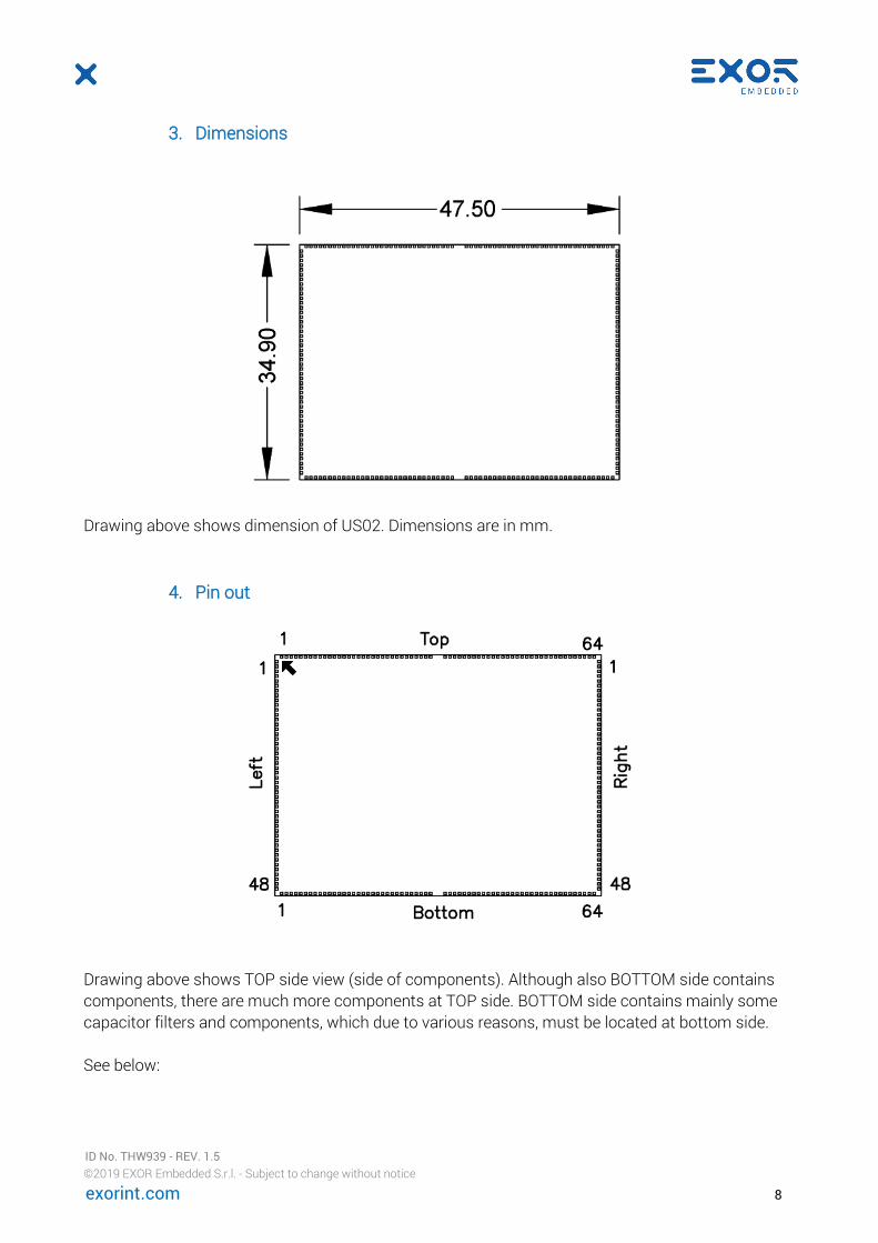
4. Pin out .......................................................................................................................................... 8
4.1. Left connector ................................................................................................................. 10 4.2. Top connector ................................................................................................................. 11 4.3 Right connector ............................................................................................................... 13 4.4 Bottom connector .......................................................................................................... 14
5 Description ............................................................................................................................... 17
5.1. Hard processors system (HPS) .................................................................................. 19 5.1.1. Dual ARM Cortex-9 CPU .................................................................................. 19 5.1.2. Embedded memory controller .......................................................................... 19 5.1.3. eMMC .................................................................................................................... 19 5.1.4. USB 2.0 support .................................................................................................. 19 5.1.5. CAN1 and CAN2 .................................................................................................. 19 5.1.6. UART1 and UART2 ............................................................................................. 19 5.1.7. HPS GPIO .............................................................................................................. 20 5.1.8. I2C ........................................................................................................................... 21
5.2. FPGA ................................................................................................................................. 21 5.2.1. Ethernet channel 1 and channel 2 ................................................................... 21 5.2.2. Video in controller ............................................................................................... 21 5.2.3. SPI1 and SPI2 ...................................................................................................... 21 5.2.4. SD card .................................................................................................................. 21 5.2.5. Audio OUT ............................................................................................................ 22 5.2.6. Video out controller ............................................................................................ 22 5.2.7. UART3 ................................................................................................................... 23 5.2.8. FPGA I/O .............................................................................................................. 23 5.2.9. LVDS channels .................................................................................................... 23
5.3. Additional circuits ........................................................................................................... 23 5.3.1. Power supply ...................................................................................................... 23 5.3.2. RTC ....................................................................................................................... 23 5.3.3. FRAM .................................................................................................................... 23 5.3.4. SEEPROM ............................................................................................................ 24 5.3.5. SPI A/D ................................................................................................................. 24
5.4. Default boot procedure ................................................................................................ 24 5.4.1. Optionally booting using QSPI from HPS ....................................................... 24
5.5. Programming-AUX 16 pins connector (solder pads) .............................................. 25 5.6. External IO “Connectors” ............................................................................................... 29 5.7 Board View ........................................................................................................................ 32

ID No. THW939 - REV. 1.5 ©2019 EXOR Embedded S.r.l. - Subject to change without notice
exorint.com 4
6. Building carrier board for hosting MicroSOM™ ................................................................. 34
6.1 Some specific signals .................................................................................................... 37 6.2 Crypto chip ....................................................................................................................... 39 6.3 Connecting with non standard chips (QUAD SPI) ..................................................... 39
7. Soldering profile ...................................................................................................................... 41

ID No. THW939 - REV. 1.5 ©2019 EXOR Embedded S.r.l. - Subject to change without notice
exorint.com 5
1. Introduction
This document is hardware presentation of microSOM™ US02.
US02 is member of EXOR’s microSOM™ family, very small but powerful PCB board, without connectors. Practically, user can consider MicroSOM™ (US02) as “a component”, which can be soldered directly in users, custom carrier board. US02 is compatible with other modules from MicroSOM™ family (see, in document THW936-2, differences respecting US01 and level of compatibility).

ID No. THW939 - REV. 1.5 ©2019 EXOR Embedded S.r.l. - Subject to change without notice
exorint.com 6

ID No. THW939 - REV. 1.5 ©2019 EXOR Embedded S.r.l. - Subject to change without notice
exorint.com 7
2. microSOM™ technology
microSOM™ is one ultra-compact SOM that introduces new connection technical similar to chip scale package of IC, that allows soldering to the main carrier board the same as other IC smt components. microSOM™ adapts connection technique Flat no-leads packages 224 contacts 0,7mm QFN (quad-flat no-leads). It is a surface-mount technology that connect ICs to the surfaces of PCB without through-holes and without expensive connectors. Perimeter lands on the package bottom provide electrical connections to the PCB. The microSOM™ has very compact size (see Figure 1A-B) and is not invasive in the design of the carrier board. The microSOM™ has especially a thickness of only 3,8 mm max, almost like the normal IC package, allowing you to create industrial products with very compact and incredibly thin profile.
Figure 1A microSOM™ outline dimension 47x35 mm Figure 1B microSOM™ thickness
CARRIER BOARD
1,6 mm microSOM
PCB thickness
3,8 mm microSOM max. module
thickness
™™
ID No. THW939 - REV. 1.5 ©2019 EXOR Embedded S.r.l. - Subject to change without notice
exorint.com 8
3. Dimensions
Drawing above shows dimension of US02. Dimensions are in mm.
4. Pin out
Drawing above shows TOP side view (side of components). Although also BOTTOM side contains components, there are much more components at TOP side. BOTTOM side contains mainly some capacitor filters and components, which due to various reasons, must be located at bottom side. See below:

ID No. THW939 - REV. 1.5 ©2019 EXOR Embedded S.r.l. - Subject to change without notice
exorint.com 9
US02 is built around four external (edge) ”connectors”. Really, these “connectors” are not true connectors, but simple soldering PADS, with pitch 0.7mm. Left and Right connector are 48 pins, while Top and Bottom are 64 pins. All signals are direct LVCMOS (+3V3) compatible, except LVDS signals. LVDS signals are coming from LVDS banks, which are supplied by +2V5. Note that also LVDS signals in some special cases (for example lack of I/O pins for some big design) can be used also for 3V3 environment (as LVTTL or LVCMOS compatible). Designer must be aware that in this case for these signals VoutHigh = +2V5 (bank supply) and must validate compatibility with input levels of external circuits. Concerning input levels, these signals although supplied with +2V5, are +3V3 tolerant. Next four chapters shows all pins, located at external “connectors”. Some signals are fixed by name (for example SPI1xx, SPI2xx, SDxx, VID_OUTxx, RGMII1xx, RGMII2xx, VID_INxx, …). These signals are connected to appropriate core inside HPS or are built inside FPGA part. Note that these names are not mandatory. It is possible in some special, custom FPGA design that these signals have some other using. The tables in next chapters show default (typical) using. Some signals (have name GPIO in Type column) are true GPIO, without some special using. These signals have various names in this tables, but these names are meaningless. These names are only inserted to show compatibility with previous Exor CPU board (UN31).

ID No. THW939 - REV. 1.5 ©2019 EXOR Embedded S.r.l. - Subject to change without notice
exorint.com 10
4.1. Left connector
Pin Name Type FPGABank/Pin Comment 1 +3V3S Supply
Supply +3V3, 5% 2 +3V3S Supply 3 +3V3S Supply 4 +3V3S Supply 5 Ch2_Tx0+
LVDS CH 2 (Transmit)
Bank 5A AA24
LVDS channel
(Transmit)
6 Ch2_Tx0- Bank 5A AA23 7 Ch2_Tx1+ Bank 5A AC24 8 Ch2_Tx1- Bank 5A AB23 9 Ch2_Tx2+ Bank 5A AE25 10 Ch2_Tx2- Bank 5A AD26 11 Ch2_Tx3+ Bank 5A AF26 12 Ch2_Tx3- Bank 5A AE26 13 Ch2_Clk+ Bank 8A E8 14 Ch2_Clk- Bank 8A D8 15 IO_4 GPIO Bank 3A AD4 16 IO_5 GPIO Bank 3B AE4 17 GND 18 SPI1_CLK
SPI1
Bank 3A Y8
SPI channel 1 used as master
19 SPI1_CS0* Bank 3A Y5 20 SPI1_CS1* Bank 3A Y4 21 SPI1_SOMI Bank 3A AA4 22 SPI1_SIMO Bank 3A AB4 23 SPI1_INT* Bank 3A AC4 24 GND 25 EN_SUPP_SD
SD Card Bank 3A AE6
SD card AUX signals
26 SD_CD* Bank 3B AF6 27 SD_WP* Bank 3B AF5 28 GND 29 SD_CLK
SD Card
Bank 3B AF4
SD card Main
signals
30 SD_CMD Bank 3B AG5 31 SD_D0 Bank 3B AG6 32 SD_D1 Bank 3B AH2 33 SD_D2 Bank 3B AH4 34 SD_D3 Bank 3B AH5 35 TOUCH_INT* INT* Bank 3B AH6 Touch interrupt* 36 GND 37 USB1_DP
USB Port 1
Via HUB
USB port 1 38 USB1_DM Via HUB 39 USB1_BUS Via HUB 40 USB1_DRVBUS Via HUB

ID No. THW939 - REV. 1.5 ©2019 EXOR Embedded S.r.l. - Subject to change without notice
exorint.com 11
41 USB2_DP
USB Port 2
Via HUB
USB port 2 42 USB2_DM Via HUB 43 USB2_BUS Via HUB 44 USB2_DRVBUS Via HUB 45 USB_OC* Over current USB Driver overcurr. 46 +3V3S Supply
Supply +3V3, 5% 47 +3V3S Supply 48 +3V3S Supply
4.2. Top connector
Pin Name Type FPGABank/Pin 1 Ch1_Clk-
LVDS CH 1 (Receive)
Bank 8A D11
LVDS channel
(Receive)
2 Ch1_Clk+ Bank 8A E11 3 Ch1_Rx3- Bank 5A Y18 4 Ch1_Rx3+ Bank 5A Y17 5 Ch1_Rx2- Bank 5A W15 6 Ch1_Rx2+ Bank 5A Y16 7 Ch1_Rx1- Bank 5A V15 8 Ch1_Rx1+ Bank 5A V16 9 Ch1_Rx0- Bank 5A Y19 10 Ch1_Rx0+ Bank 5A AA20 11 GND 12 VBB Battery supply Ext. battery 2V-5.5V 13 SCL HPS Bank7B C18 14 SDA HPS Bank7B A19 15 SYS_RST_OUT* HPS Bank7D E4 Reset OUT* (out**) 16 RES_IN* Reset IN* (in**) 17 EN_EXT_IO EN_EXT_IO (out**) 18 PFAIL_IN* HPS Bank7C B12 PFAIL_IN (in**) 19 AIN0
Five analog inputs 0---+1V8
20 AIN1 21 AIN2 22 AIN3 23 AIN4 24 AGND AGND 25 GND 25 EN_VDD
Video out control AUX
Bank 3A U10 Video out AUX
signals 27 DIMM Bank 3A V10 28 EN_BL Bank 3B T11 29 VID_ENAB
Video out Main control
Bank 4A AH8 Video out control
signals 30 VID_HSYNC Bank 4A AG8 31 VID_VSYNC Bank 4A AH9 32 VID_VCLK Bank 4A AG9 33 GND

ID No. THW939 - REV. 1.5 ©2019 EXOR Embedded S.r.l. - Subject to change without notice
exorint.com 12
34 VID_D16
Video out data
Bank 4A AG10
Vid_out_D16-D19 35 VID_D17 Bank 4A AG11 36 VID_D18 Bank 4A AH11 37 VID_D19 Bank 4A AH12 38 GND 39 VID_D20
Video out data
Bank 4A AH13
Vid_out_D20-D23 40 VID_D21 Bank 4A AH14 41 VID_D22 Bank 4A AH16 42 VID_D23 Bank 4A AH17 43 GND 44 VID_D0
Video out data
Bank 4A AH18
Vid_out_D0-D3 45 VID_D1 Bank 4A AH19 46 VID_D2 Bank 4A AG19 47 VID_D3 Bank 4A AH21 48 GND 49 VID_D4
Video out data
Bank 4A AG21
Vid_out_D4-D7 50 VID_D5 Bank 4A AH22 51 VID_D6 Bank 4A AF23 52 VID_D7 Bank 4A AG24 53 GND 54 VID_D8
Video out data
Bank 4A AF25
Vid_out_D8-D11 55 VID_D9 Bank 4A AG25 56 VID_D10 Bank 4A AG26 57 VID_D11 Bank 4A AF27 58 GND 59 VID_D12
Video out data
Bank 4A AF28
Vid_out_D12-D15 60 VID_D13 Bank 4A AG28 61 VID_D14 Bank 4A AH27 62 VID_D15 Bank 4A AH26 63 GND 64 +3V3S Supply Supply +3V3, 5%
(**) These signals are system control I/O. SYS_RST_OUT* is system reset, coming from circuits inside MicroSOM™. RES_IN* is (optionally) external RESET input signal (including reset KEY) EN_EXT_IO (Power Good) is control out (from US02). User should use this signal to enable supply for I/O peripherals at carrier board. See in the rest of documents more description for this signal. PFAIL_IN* is optional PFAIL interrupt* to inform US02 about optional Power Fail.

ID No. THW939 - REV. 1.5 ©2019 EXOR Embedded S.r.l. - Subject to change without notice
exorint.com 13
4.3 Right connector
Pin Name Type Used in US02
1 +3V3S Supply Supply +3V3, 5% 2 GND 3 RX1
UART1
HPS Bank7B B19
UART1 4 CTS1 HPS Bank7B A18 5 RTS1 HPS Bank7B C17 6 TX1 HPS Bank7B C16 7 RX2
UART2
HPS Bank7B C19
UART2 8 CTS2 HPS Bank7B B18 9 RTS2 HPS Bank7B J17 10 TX2 HPS Bank7B B16 11 GND 12 RX3
UART3
Bank 3B U11
UART3 13 CTS3 Bank 3B T13 14 RTS3 Bank 3A Y11 15 TX3 Bank 3A AA11 16 CAN1_RX
CAN1 HPS Bank7B A17
CAN1 17 CAN1_TX HPS Bank7B H17 18 CAN2_RX
CAN2 HPS Bank7B A20
CAN2 19 CAN2_TX HPS Bank7B J18 20 GND 21 RGMII1_RXD0
RGMII/RMII CH1
Bank 4A U13 RGMII/RMII
CH1 22 RGMII1_RXD1 Bank 4A V13 23 RGMII1_RXD2 Bank 4A U14 24 RGMII1_RXD3 Bank 4A W14 25 GND 26 RGMII1_RXCLK RGMII/RMII
CH1 Bank 4A AA13 RGMII/RMII
CH1 27 RGMII1_RXDV Bank 4A AA15 28 GND 29 RGMII1_TXD0
RGMII/RMII CH1
Bank 4A AA18 RGMII/RMII
CH1 30 RGMII1_TXD1 Bank 4A AA19 31 RGMII1_TXD2 Bank 4A AD17 32 RGMII1_TXD3 Bank 4A AD19 33 GND 34 RGMII1_TXCLK
RGMII/RMII CH1
Bank 4A AE20 RGMII/RMII
CH1 35 RGMII1_TXEN Bank 4A AF21 36 RGMII1_INT* Bank 4A AG23 37 GND 38 RGMII_MDIO_C RGMII/RMII
control Bank 4A AH24
MDIO D/C control 39 RGMII_MDIO_D Bank 4A AH23 40 GND 41 RGMII2_RXD0 RGMII/RMII
CH2 Bank 4A AF20 RGMII/RMII
CH2 42 RGMII2_RXD1 Bank 4A AF18

ID No. THW939 - REV. 1.5 ©2019 EXOR Embedded S.r.l. - Subject to change without notice
exorint.com 14
43 RGMII2_RXD2 Bank 4A AG18 44 RGMII2_RXD3 Bank 4A AE17 45 GND 46 RGMII2_RXCLK RGMII/RMII
CH2 Bank 4A AF17 RGMII/RMII
CH2 47 +3V3S Supply
Supply +3V3, 5% 48 +3V3S Supply
Signal name: Used in RGMII as: Used in RMII as: RGMII1_RXD0 RGMII1_RXD0 RMII1_RXD0 RGMII1_RXD1 RGMII1_RXD1 RMII1_RXD1 RGMII1_RXD2 RGMII1_RXD2 RGMII1_RXD3 RGMII1_RXD3 RGMII1_RXCLK RGMII1_RXCLK RMII1_REFCLK RGMII1_RXDV RGMII1_RXDV RMII1_CRS_DV RGMII1_TXD0 RGMII1_TXD0 RMII1_TXD0 RGMII1_TXD1 RGMII1_TXD1 RMII1_TXD1 RGMII1_TXD2 RGMII1_TXD2 RGMII1_TXD3 RGMII1_TXD3 RGMII1_TXCLK RGMII1_TXCLK RMII1_RX_ERROR RGMII1_TXEN RGMII1_TXEN RMII1_TXEN RGMII1_INT* RGMII1_INT* RMII1_INT* RGMII_MDIO_C RGMII_MDIO_CLK RMII_MDIO_CLK RGMII_MDIO_D RGMII_MDIO_DATA RMII_MDIO_DATA
Table above shows using generic Ethernet signals for RGMII or RMII for channel 1.
4.4 Bottom connector
Pin Name Type Used in US02
1 +3V3S Supply Supply +3V3, 5%
2 +3V3S Supply 3 IO_3 GPIO HPS Bank7C A14 4 IO_2 GPIO HPS Bank7C A13 5 IO_1 GPIO HPS Bank7C A12 6 BUZZER GPIO Bank 3B AH3 Buzzer 7 GND 8 EN_3W3_SW GPIO HPS Bank7C A11 9 OUT_STDBY GPIO HPS Bank7D A7 10 EN_STDBY GPIO HPS Bank7D A8 11 GP_PUSH_BUTT GPIO HPS Bank7C A9 12 CAN_SEL GPIO HPS Bank7C A15

ID No. THW939 - REV. 1.5 ©2019 EXOR Embedded S.r.l. - Subject to change without notice
exorint.com 15
13 PL2_B_I2C_EN GPIO HPS Bank7C A16 14 PL2_RES GPIO HPS Bank7D B14 15 PL2_T_I2C_EN GPIO HPS Bank7D C14 16 GND 17 PL1_B_I2C_EN GPIO HPS Bank7C C15 18 P11_RES GPIO HPS Bank7C E16 19 PL1_T_I2C_EN GPIO HPS Bank7C D17 20 RXEN0 GPIO HPS Bank7D H16 21 DXEN0 GPIO HPS Bank7D J13 22 MODE0 GPIO HPS Bank7D J12 23 DL
Out HPS Bank7C J14 Used for external
LED 24 FAULT HPS Bank7C J15 25 BAT_CHK GPIO HPS Bank7D J16 26 VIDIN_AUX0
Video IN AUX or GPIO
Bank 3B AE9 27 VIDIN_AUX1 Bank 3B AD10 28 VIDIN_AUX2 Bank 3B AF11 29 VIDIN_AUX3 Bank 3B AE11 30 GND 31 VIDIN_D0
Video IN ITY 656
Bank 3B AE12 Video IN ITY 656
32 VIDIN_D1 Bank 3B AE7 33 VIDIN_D2 Bank 3B AF7 34 VIDIN_D3 Bank 3B AE8 35 GND 36 VIDIN_D4
Video IN ITY 656
Bank 3B AF8
Video IN ITY 656
37 VIDIN_D5 Bank 3B AF9 38 VIDIN_D6 Bank 3B AD11 39 VIDIN_D7 Bank 3B AD12 40 VIDIN_CLK Bank 3B AF10 41 GND 42 SPI2_INT*
SPI2
Bank 4A AE19
SPI2 used as master or slave
43 SPI2_SIMO Bank 4A AG20 44 SPI2_SOMI Bank 4A AD20 45 SPI2_CS1* Bank 4A AE22 46 SPI2_CS0* Bank 4A AF22 47 SPI2_CLK Bank 4A AC22 48 GND 49 AUDA_BCLK
Audio I2S
Bank 4A AE23 I2S Audio
50 AUDA_DIN Bank 4A AD23 51 AUDA_FSX Bank 4A AE24 52 AUDA_DOUT Bank 4A AC23 53 GND 54 RGMII2_INT*
RGMII/RMII CH2
Bank 3B W11 RGMII/RMII
CH2 55 RGMII2_TXEN Bank 4A AG13 56 RGMII2_TXCLK Bank 4A AG14 57 GND 58 RGMII2_TXD3 RGMII/RMII Bank 4A AF13 RGMII/RMII

ID No. THW939 - REV. 1.5 ©2019 EXOR Embedded S.r.l. - Subject to change without notice
exorint.com 16
59 RGMII2_TXD2 CH2 Bank 4A AE15 CH2 60 RGMII2_TXD1 Bank 4A AG15 61 RGMII2_TXD0 Bank 4A AF15 62 GND 63 RGMII2_RXDV RGMII/RMII
CH2 Bank 4A AG16 RGMII/RMII
CH2 64 +3V3S Supply +3V3, 5%
Signal name: Used in RGMII as: Used in RMII as: RGMII2_RXD0 RGMII2_RXD0 RMII2_RXD0 RGMII2_RXD1 RGMII2_RXD1 RMII2_RXD1 RGMII2_RXD2 RGMII2_RXD2 RGMII2_RXD3 RGMII2_RXD3 RGMII2_RXCLK RGMII2_RXCLK RMII2_REFCLK RGMII2_RXDV RGMII2_RXDV RMII2_CRS_DV RGMII2_TXD0 RGMII2_TXD0 RMII2_TXD0 RGMII2_TXD1 RGMII2_TXD1 RMII2_TXD1 RGMII2_TXD2 RGMII2_TXD2 RGMII2_TXD3 RGMII2_TXD3 RGMII2_TXCLK RGMII2_TXCLK RMII2_RX_ERROR RGMII2_TXEN RGMII2_TXEN RMII2_TXEN RGMII2_INT* RGMII2_INT* RMII2_INT*
Table above shows using generic Ethernet signals for RGMII or RMII for channel 2.

ID No. THW939 - REV. 1.5 ©2019 EXOR Embedded S.r.l. - Subject to change without notice
exorint.com 17
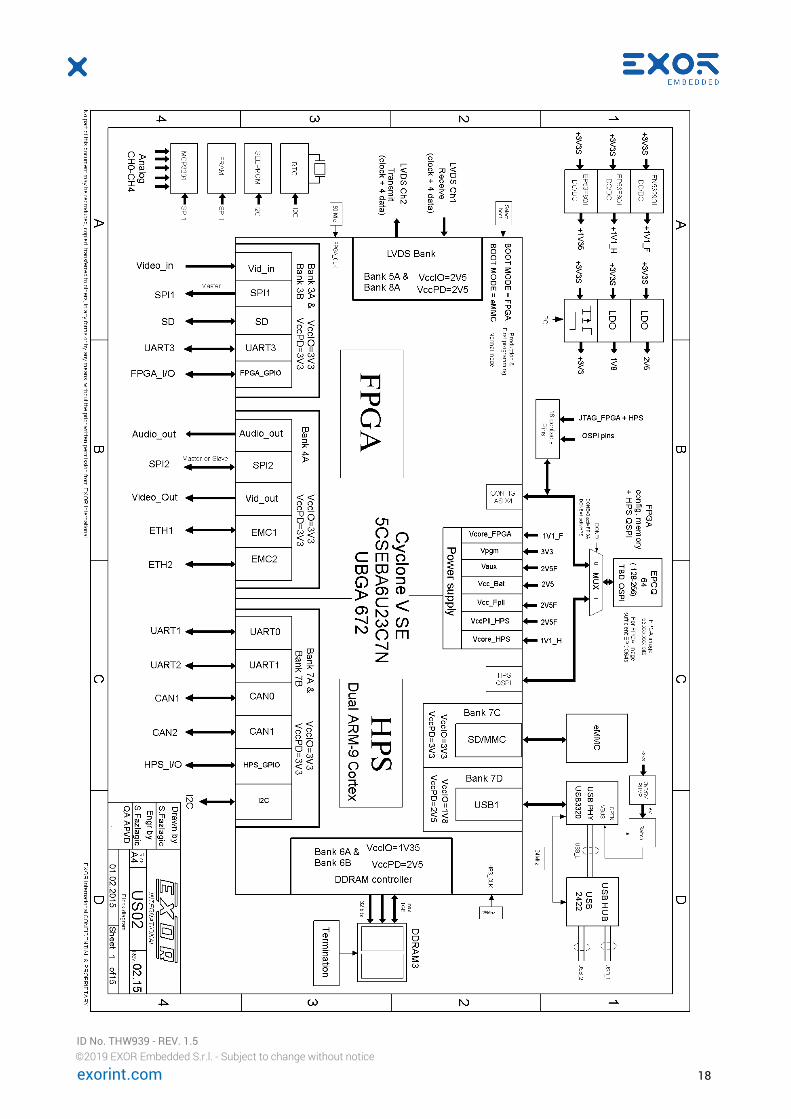
5 Description
US02 is built around SOC (System on chip) CYCLONE V_5CSEBAX (uBGA 672 pins). Possible options are A2, A4, A5 and A6, which have various FPGA cells numbers. Default US02 is based at version A2, which is smallest version 5CSEBA2U23 (672 pins) CYCLONE V_5CSEBAX is real FPGA with incorporated dual core ARM 9 processor. Using this approach is possible to get high level of integration, customization and PCB minimization in US02. Drawing at next pages shows block diagram of this board. Block diagram shows that SOC contains 0f two parts:
1) HPS 2) FPGA
HPS is “hard wired” part (core) of SOC, which contains two core ARM 9 processor and provides (contains cores):
• Interface towards DDRAM • Interface towards eMMC • USB interface • Some peripherals (UARTs, CANS, I2C…)
HPS contains also some other cores (for example ETHERNET), but only some can be used contemporary (due to lack of pins no all possible configurations can be used contemporary). In US02 are used only these peripherals (cores), presented at block diagram. FPGA is configurable part, which contains other peripherals (cores) and it is possible also change and accommodate for particularly needs. See details in rest of chapter.
ID No. THW939 - REV. 1.5 ©2019 EXOR Embedded S.r.l. - Subject to change without notice
exorint.com 18

ID No. THW939 - REV. 1.5 ©2019 EXOR Embedded S.r.l. - Subject to change without notice
exorint.com 19
5.1. Hard processors system (HPS)
5.1.1. Dual ARM Cortex-9 CPU
US02 is based at Dual ARM Cortex-9 core located in SOC. in HPS part. This approach (SOC) provides tight integration of a dual-core ARM Cortex-A9 MP Core processor, hard IP, and an FPGA in a single Cyclone V system-on-a-chip (SoC) FPGA. Supports over 128 Gbps peak bandwidth with integrated data coherency between the processor and the FPGA fabric
5.1.2. Embedded memory controller
HPS contains embedded memory controller with support for various memory types. In US02 is used DDRAM3 (800 Mb data rate). In US02 is used 32 bits bus for memory (two 16 bits memory chips) to provide high bandwidth. Can be used total MAX 1GByte. Note that the same memory is used for System and Video memory (Unified memory)
5.1.3. eMMC
HPS supports eMMC (embedded MMC) chip. It is used high speed SD/MMC bus in 4/8 bits mode for eMMC. In US02 embedded eMMC is used as main OS memory. It is used 169 balls chip (it covers also 153 ball standard), which provides using large spectrum of density (up to 128 GB) of various manufacturers.
5.1.4. USB 2.0 support
Although HPS contains two embedded USB channels, due to pins using constrains, is used one USB channel. It is added an external USB transceiver USB3320 and two ports HUB (USB 2422). This way, user can see two USB channels (Note that is possible only HOST mode using).
5.1.5. CAN1 and CAN2
Both CAN cores from HPS are used for system CAN1 and CAN2 channels
5.1.6. UART1 and UART2
Two embedded cores (UART0 and UART1) from HPS are used for system UART1 and UART2 channels

ID No. THW939 - REV. 1.5 ©2019 EXOR Embedded S.r.l. - Subject to change without notice
exorint.com 20
5.1.7. HPS GPIO
Various GPIO, defined in Micro SOM standard, are built using GPIO from HPS. Under HPS GPIO we consider various generic input/output signals. These signals are available to user as GPIO. Table below shows these signals with some “default meanings”. This “default meanings” is chosen only to show MicroSOM™ and previous EXOR’s HMI CPU (UN31) compatibility and it is not mandatory. For example, signals PL1XXX and PL2XXX in table below are named in this way only to provide for support PLXX modules, but if these modules are not used, user can, in his custom case, use these signals as standard GPIO.
Position Signal Name Description Bottom Pin 12 CAN_SEL (1) Bottom Pin 25 BATT_CHK (2) Bottom Pin 9 OUT_STDBY (3) Bottom Pin 5 IO1 (4) Bottom Pin 4 IO2 (5) Bottom Pin 3 IO3 (6)
Bottom Pin 17 PL1_B_I2C_EN (7) Bottom Pin 18 PL1_RES (8) Bottom Pin 19 PL1_T_I2C_EN (9) Bottom Pin 13 PL2_B_I2C_EN (10) Bottom Pin 14 PL2_RES (11) Bottom Pin 15 PL2_T_I2C_EN (12) Bottom Pin 8 EN_3V3_SW (13)
Bottom Pin 10 EN_STDBY (14) Bottom Pin 11 GP_PUSH_BUTTON (15) Bottom Pin 20 RXEN0 (16) Bottom Pin 21 DXEN0 (17) Bottom Pin 22 MODE0 (18)
(1) Used for signal CAN_SEL (CAN SELECT for exchange CAN at carrier board) (2) BATT_CHK (For Battery Check signal) (3) OUT_STDBY (Signal OUT_STDBY) (4) I/O1 (GPIO) (5) I/O2 (GPIO) (6) I/O3 (GPIO) (7) PL1_B_I2C_EN (Signal PL1 Bottom I2C enable) (8) PL1_RES (Signal PL1 reserve) (9) PL1_T_I2C_EN (Signal PL1 Top I2C enable) (10) PL2_B_I2C_EN (Signal PL2 Bottom I2C enable) (11) PL2_RES (Signal PL2 reserve)

ID No. THW939 - REV. 1.5 ©2019 EXOR Embedded S.r.l. - Subject to change without notice
exorint.com 21
(12) PL2_T_I2C_EN (Signal PL2 Top I2C enable) (13) EN_3V3_SW (Signal Enable switch 3V3) (14) EN_STDBY (Signal Enable standby) (15) GP_PUSH_BUTTON (General purpose Push button) (16) RXEN0 (Signal for programmable Uart configuration) (17) DXEN0 (Signal for programmable Uart configuration) (18) MODE0 (Signal for programmable Uart configuration)
5.1.8. I2C
One of three I2C controllers in HPS is used as system I2C controller in US02
5.2. FPGA
Second part of US02 SOC is FPGA. FPGA part provides incorporating other cores, not existing in HPS. There are various FPGA HPS and HPS FPGA bridges as part of SOC (inside SOC). Some cores from HPS can be routed via FPGA part.
5.2.1. Ethernet channel 1 and channel 2
FPGA part contains pins for two Ethernet channels (RGMI or RMI), but really in US02 are used IP cores EMC1 and EMC2 from HPS, which are only routed via FPGA.
5.2.2. Video in controller
FPGA contains IP core for Video in controller ITU 656. There also reserved 4 AUX bits for supporting other video formats (TBD).
5.2.3. SPI1 and SPI2
FPGA incorporates SPI cores for two external SPI interfaces with two CS*. SPI 1, in addition, is used also for ON board (located inside US02) SPI peripherals (FRAM and AD converter). It means that SPI channel really supports four SPI peripherals in master mode (two inside US02 and two external). SPI2 channel can be used as master or slave.
5.2.4. SD card
FPGA contains IP core for external SD controller.

ID No. THW939 - REV. 1.5 ©2019 EXOR Embedded S.r.l. - Subject to change without notice
exorint.com 22
5.2.5. Audio OUT
FPGA incorporates Audio OUT I2S.
5.2.6. Video out controller
FPGA contains IP core for Video out controller 24bits. This controller is 16 or 24 bits, in order to be compatible with US01. Table below shows Video out bits mapping
Bit position Color 16 bits Color 24 bits
LCD_D0 B1 R3 LCD_D1 B2 R4 LCD_D2 B3 R5 LCD_D3 B4 R6 LCD_D4 B5 R7 LCD_D5 G0 G2 LCD_D6 G1 G3 LCD_D7 G2 G4 LCD_D8 G3 G5 LCD_D9 G4 G6
LCD_D10 G5 G7 LCD_D11 R1 B3 LCD_D12 R2 B4 LCD_D13 R3 B5 LCD_D14 R4 B6 LCD_D15 R5 B7 LCD_D16 R2 LCD_D17 B2 LCD_D18 R1 LCD_D19 G1 LCD_D20 B1 LCD_D21 R0 LCD_D22 G0 LCD_D23 B0

ID No. THW939 - REV. 1.5 ©2019 EXOR Embedded S.r.l. - Subject to change without notice
exorint.com 23
5.2.7. UART3
FPGA also contains IP core for the third system UART (UART3).
5.2.8. FPGA I/O
There are two GPIO, coming from FPGA part
Position Signal Name Description Left Pin 15 IO_4 GPIO Left Pin 16 IO_5 GPIO
5.2.9. LVDS channels
FPGA contains also two five pair’s channels (four data + CLK). One channel is Receive and second one is Transmit.
5.3. Additional circuits
5.3.1. Power supply
US02 is using three ultra-small DC/DC converters from ENPIRION. Input voltage is +3V3. In board are used:
• Enpirion EN5329QI (2A) for generating +1V1 voltage for FPGA core • Enpirion EO53F8QI (1.5A) for generating +1V1 voltage for HPS core • Enpirion EO53F8QI (1.5A) for generating +1V35 voltage for DDRAM3L
In addition, are used two Low noise LDO (for +1V8 and +2V5)
5.3.2. RTC
For US02 MicroSOM™ for RTC purpose is used M41T83 RTC chip. Chip is back upped with Vbb.
5.3.3. FRAM
For US02 MicroSOM™ is used FRAM FM25L512. This chip is connected via SPI channel 1.
ID No. THW939 - REV. 1.5 ©2019 EXOR Embedded S.r.l. - Subject to change without notice
exorint.com 24
5.3.4. SEEPROM
US02 MicroSOM™ contains one standard I2C SEEPROM.
5.3.5. SPI A/D
US02 MicroSOM™ contains also five channels SPI 12 bits A/D converter. SPI converter is connected via SPI 1 channel. Analog input range is 0-1.8V.
5.4. Default boot procedure
For booting (configuration) FPGA is provided one X4 SPI NOR Flash. Booting procedure is:
1) FPGA is booted always from QSPI after power up (control pin for MUX is under pull down resistors and flow signals is between FPGA and QSPI)
2) After FPGA is configured, HPS is booted either from FPGA or from eMMC. 3) Selection is done via bit BOOTSELECT2 which is available at 16 pins AUX conn (pin 11). The
actual option is booting the HPS from FPGA. 4) After configuration and booting, HPS takes control of QSPI for writing and reading, using
embedded QSPI controller in HPS. First programming: For first (factory) programming is used JTAG available at AUX 16 pins connector.
5.4.1. Optionally booting using QSPI from HPS
Due to specific configuration (existing of multiplexer for QSPI (presented below)) there is also possibility of different boot mode (boot HPS from QSPI. Via QSPI MUX we have access to QSPI, so it is possible the next procedure:
• HPS boots from QSPI • HPS enter in FPGA configuration via embedded FPGA manager (HPS configures FPGA)
Practically, this procedure is inverted respecting original default boot model. See drawing below.
ID No. THW939 - REV. 1.5 ©2019 EXOR Embedded S.r.l. - Subject to change without notice
exorint.com 25
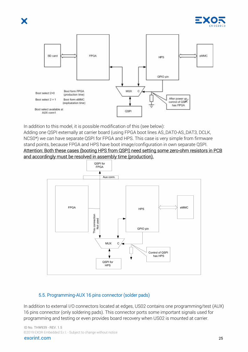
In addition to this model, it is possible modification of this (see below): Adding one QSPI externally at carrier board (using FPGA boot lines AS_DAT0-AS_DAT3, DCLK, NCS0*) we can have separate QSPI for FPGA and HPS. This case is very simple from firmware stand points, because FPGA and HPS have boot image/configuration in own separate QSPI. Attention: Both these cases (booting HPS from QSPI) need setting some zero-ohm resistors in PCB and accordingly must be resolved in assembly time (production).
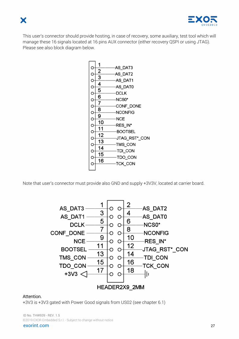
5.5. Programming-AUX 16 pins connector (solder pads)
In addition to external I/O connectors located at edges, US02 contains one programming/test (AUX) 16 pins connector (only soldering pads). This connector ports some important signals used for programming and testing or even provides board recovery when US02 is mounted at carrier.
FPGA HPS eMMC
MUX
Control of QSPI has HPS
C
GPIO pin
QSPI for FPGA
QSPI for HPS
Aux conn.
This
con
nect
ion
Not
use
d

ID No. THW939 - REV. 1.5 ©2019 EXOR Embedded S.r.l. - Subject to change without notice
exorint.com 26
This connector contains:
• JTAG connector signals • Some FPGA related signals plus QSPI signals.
Using JTAG is not mandatory. Also using QSPI signal for final user is not mandatory but is highly recommended to follow suggestions in this chapter. Following these rules in carrier board building, user will have great help in US02 recovery. Don’t forget that US02 is soldered, so recovery without additional tools is not simple. Drawing below shows this concepts and signals, assigned to this 16 pins AUX connector (pads).
Take attention to JTAG connection between HPS and FPGA. Both parts of CPU have own JTAG channels but are connected in chain. Drawing below shows signals included in 16 pins AUX programming connector.
1. Six signals for QSPI direct access. 2. Some system signals related for configuration. 3. JTAG signals.
In order to take advantage of this 16 AUX pin connector, user should add in carrier board own recovery connector connected directly to these 16 pins of AUX connector.
ID No. THW939 - REV. 1.5 ©2019 EXOR Embedded S.r.l. - Subject to change without notice
exorint.com 27
This user’s connector should provide hosting, in case of recovery, some auxiliary, test tool which will manage these 16 signals located at 16 pins AUX connector (either recovery QSPI or using JTAG). Please see also block diagram below.
Note that user’s connector must provide also GND and supply +3V3V, located at carrier board.
Attention. +3V3 is +3V3 gated with Power Good signals from US02 (see chapter 6.1)

ID No. THW939 - REV. 1.5 ©2019 EXOR Embedded S.r.l. - Subject to change without notice
exorint.com 28
It is not +3V3S (+3V3 System), which supplies microSOM, but +3V3 gated with Power Good at carrier (this supply already exists at carrier). Practically, one 18 pins header should be OK. In case that user wants to use this feature (it is not mandatory), selection of recovery connector depends of user’s preference. One double row header 2mm is good solution. In addition to this connector, user should always provide using SD card. Even in case that custom design is not using SD card, user should place reserved /Test connector for mounting SD/microSD card (see drawing below). The same discussion is valid for +3V3 (+3V3 must be gated with Power Good).

ID No. THW939 - REV. 1.5 ©2019 EXOR Embedded S.r.l. - Subject to change without notice
exorint.com 29
Drawing above shows suggested solution.
5.6. External IO “Connectors”
Two next pages show “connectors” for LEFT_TOP and BOTTOM_RIGHT side. These drawings are completely the same as tables presented before and goal of these drawings is only to give user one better view and position of signals.

ID No. THW939 - REV. 1.5 ©2019 EXOR Embedded S.r.l. - Subject to change without notice
exorint.com 30

ID No. THW939 - REV. 1.5 ©2019 EXOR Embedded S.r.l. - Subject to change without notice
exorint.com 31

ID No. THW939 - REV. 1.5 ©2019 EXOR Embedded S.r.l. - Subject to change without notice
exorint.com 32
5.7 Board View
The next two pictures below show TOP and BOTTOM side of US02

ID No. THW939 - REV. 1.5 ©2019 EXOR Embedded S.r.l. - Subject to change without notice
exorint.com 33
Picture above shows bottom side of US02. Take attention to I/O pads at board edges and pads for 16 pins programming/AUX connector. Attention: It is board through view (from TOP side view, where TOP side is transparent).

ID No. THW939 - REV. 1.5 ©2019 EXOR Embedded S.r.l. - Subject to change without notice
exorint.com 34
6. Building carrier board for hosting MicroSOM™
This chapter shows building MicroSOM™ footprint (shape) at carrier board, where MicroSOM™ will be soldered. Building shape is fairly simple because pin positions are full symmetric respecting board edges (IO pins) and virtual board center. Shortly, user must:
• Create shape outline and board hole inside. • Create IO pads at board edges (64 + 48 + 64 + 48). • Create 16 pads for Programming/AUX connector.
Follow this procedure for build appropriate carrier shape for MicroSOM™ shape:
1) Draw rectangle 47.50 mm x 34.90 mm (dimensions of MicroSOM™)
2) Place 48 rectangle pins (33mil x 20 mil) for Left and Right sides (first PAD center is 1mm from Top edge and 0.175 mm from Left/Right edge).
3) Place 2 x 32 rectangle (20mil x 33 mil) pins for Top and Bottom sides (first PAD center is
1mm from Left side and 0.175mm from Top/Bottom edge). Note that between pins 32 and 33 is empty space 2.1mm (center to center).
4) Place for programming / AUX connector 16 pins rectangle 27.5 mil x 31.5 mil (0.6 mm x
0.8mm). Center pin to pin distance is 1 mm. First pin center is: 7.75 mm from left edge and 5.70mm from TOP edge
5) Provide PCB hole 35.50mm X 23.50mm. Note that PCB hole is not symmetric in Y axis,
respecting virtual board center. TOP side of carrier (under MicroSOM™) CAN be used for routing.
6) Provide some arrow at silk screen near LEFT TOP angle for board orientation (origin).
See detailed drawings for building appropriate shape for carrier at next pages.
For IO pads (board edges): Solder mask shape is 4 mils bigger of PAD (all edges) Solder past shape is the same as PAD
For 16 Programming/AUX pads: Solder mask shape is 5 mils bigger of PAD (all edges) Solder past shape is the same as PAD

ID No. THW939 - REV. 1.5 ©2019 EXOR Embedded S.r.l. - Subject to change without notice
exorint.com 35

ID No. THW939 - REV. 1.5 ©2019 EXOR Embedded S.r.l. - Subject to change without notice
exorint.com 36
Picture below shows one typical carrier board for MicroSOM™.

ID No. THW939 - REV. 1.5 ©2019 EXOR Embedded S.r.l. - Subject to change without notice
exorint.com 37
6.1 Some specific signals
This chapter describes some specific signals (system signals), important in carrier board building. Drawing below shows typical using these signals: MicroSOM™ is supplied by +3V3S (system) supply (+3V3 +- 5 %)

ID No. THW939 - REV. 1.5 ©2019 EXOR Embedded S.r.l. - Subject to change without notice
exorint.com 38
1) VBB is input for connecting to some Battery source, used for RTC. Typical are used Lithium battery, Lithium rechargeable or Super CAP. Range is 2V-5.5V. In case of rechargeable battery or Super CAP, user must provide additional circuits at carrier board.
2) Analog inputs. MicroSOM™ contains block of five analog inputs and Analog GND. Signals
ranhe is 0V-1.8V.
3) SYS_RESET_OUT* is standard RESET_OUT* signal for resetting external circuits located at carrier board.
4) RES_IN* is optionally RESET_IN* (Max +3V3, active 0) signal for whole system, coming from
carrier board. For example, can be used standard CPU supervisors, or simple manual RESET key. Using external circuits is optional, because MicroSOM™ contains embedded power on RESET.
5) PFAIL_INT* is optionally PFAIL_INT*, for interrupting CPU in case of early power supply
power detection. It could be important for backup critic application where early power down event can be used for file or application closing.
6) EN_EXT_IO (Power Good) is mandatory signal (out from MicroSOM™, active high) to enable
supply auxiliary circuits at carrier board. MicroSOM™ is supplied by +3V3S (system) from

ID No. THW939 - REV. 1.5 ©2019 EXOR Embedded S.r.l. - Subject to change without notice
exorint.com 39
carrier board but supply for circuits at carrier must be controlled by these signals to respect power up procedure for CPU at MicroSOM™.
6.2 Crypto chip
MicroSOM™ can be used with external Crypto chip AT97SC3205 per Pubblic-Key Chryptography (PKCS) function. Crypto chip is not part of MicroSOM™, but in case that system needs it, this document describes also Crypto chip as part of MicroSOM™ interface and shows how is connected. Practically, Crypto chip is part of carrier board and is connected to SPI 1 (master) channel of MicroSOM™ (used second SPI CS*) Drawing below shows connection for SPI based crypto chip. One external CS* from SPI1 channel is used for Crypto chip and one as generic (CS0*). In case that Crypto chip is not used, SPI1_CS1* is available as generic (CS1*).
6.3 Connecting with non standard chips (QUAD SPI)
Chapters before are based at default US02 option (see block diagram, presented. It is also noted that various GPIO are really true GPIO but is case that user has need for some special interface, not native supported by US02, it is fairly simple realize, due to FPGA nature of US02. For example, we can take QUAD SPI interface (see below). It is obviously one special, custom case. To realize this design, we must build QUAD SPI core inside FPGA. For connecting to external pins solutions are:
1) Use standard GPIO pins (pins non dedicated to any default interface) 2) Use pins of some standard interface (but non used in this custom application)

ID No. THW939 - REV. 1.5 ©2019 EXOR Embedded S.r.l. - Subject to change without notice
exorint.com 40
GPIO pins, nearly all (except IO_4 and IO_5), are coming from HPS parts. Due to inherent Altera SOC chip features, it is possible route FPGA signals via HPS pins (solution1). Other solution is use some of “standard” pins momentary not used (for example Video input or Video D17-D23 in case of using 16-bit interface or some other).

ID No. THW939 - REV. 1.5 ©2019 EXOR Embedded S.r.l. - Subject to change without notice
exorint.com 41
7. Soldering profile
MicroSOM board must be attached to the host printed circuit board (PCB) using industry standard reflow processes. Recommended solder paste stencil thickness is 150um to ensure solder joint reliability. To avoid component damage, please consider these reflow parameters:
- Preheat and cool-down ramps should not exceed 3°C/s to prevent internal component failures due to thermal stress;
- The reflow temperature must exceed the nominal melting point of the solder paste for at least 30 seconds, not to exceed 90 seconds;
- Maximal peak body temperature is 260°C; - The time reflow within 5°C of peak temperature must not to exceed 30 seconds;
MicroSOM board are moisture sensitive and should be handled within proper MSL 3 guidelines (JEDEC standard J-STD-020) to avoid damage from moisture absorption and exposure to solder reflow temperatures that can result in yield and reliability degradation. Once the package is opened, maintain the following conditions:
- Relative humidity <50%, temperature 20-25 ºC - Fingerprints must be avoided (wear gloves) - Do not expose the boards to a corrosive gas or liquid environment - We suggest a pre-dry step according to IPC-1601 before assembly - The devices should go through reflow within 72 hours, if conditions are not met, baking is
required before board mounting - If baking is required, devices should be baked for a minimum of 8 hours at 120ºC. - Unused board can either be baked and dry-packed first before storage, or they can be baked
just before the next board assembly. Picture below shows our typical soldering thermal profile.