Embed Size (px)
Citation preview


MICROSCALE HEAT CONDUCTION IN
INTEGRA TED CIRCUITS AND THEIR
CONSTITUENT FILMS

MICROSYSTEMS
Series Editor Stephen D. Senturia
Massachusetts Institute o/Technology
Editorial Board
Roger T. Howe, University of California, Berkeley D. Jed Harrison, University of Alberta Hiroyuki Fujita, University of Tokyo Jan-Alee Schweitz, Uppsala University
Books in the Series
MICROFABRICATION IN TISSUE ENGINEERING AND BIOARTIFICIAL ORGANS
Sangeeta Bhatia ISBN: 0-7923-8566-7
MICROMACHINED ULTRASOUND·BASED PROXIMITY SENSORS M.R. Hornung, O. Brand ISBN: 0-7923-8508
BRINGING SCANNING PROBE MICROSCOPY UP TO SPEED S.C. Minne, S.R. Manalis, C.F. Quate ISBN: 0-7923-8466-0
MICROCANTILEVERS FOR ATOMIC FORCE MICROSCOPE DATA STORAGE
B.W.Chui ISBN: 0-7923-8358-3
METHODOLOGY FOR THE MODELING AND SIMULATION OF MICROSYSTEMS
B. Romanowicz ISBN: 0-7923-8306-0

MICROSCALE HEAT CONDUCTION IN
INTEGRA TED CIRCUITS AND THEIR
CONSTITUENT FILMS
By
Y. Sungtaek Ju, Ph.D. Stanford University
Kenneth E. Goodson, Ph.D. Stanford University
~.
" SPRINGER SCIENCE+BUSINESS MEDIA, LLC

Library of Congress Cataloging-in-Publication Data
Ju. Y. Sungtaek, 1970-Microscale beat conduction in integrated circuits and their constituent films 1 by Y. Sungtaek Ju, Kenneth E. Goodson. p. cm. -- (Microsystems ; 6)
Includes bibliographical references. ISBN 978-1-4613-7374-2 ISBN 978-1-4615-5211-6 (eBook) DOI 10.1007/978-1-4615-5211-6 1. Thin film transistors. 2. Semiconductors --Cooling. 3. Heat
-Transmission. 4. Silicon-on-insulator technology. 1. Goodson, Kenneth E., 1967- . II. Title. III. Series: Microsystems (Series) ; 6. TK7871. 96.T45JB 1999 621.3815--dc21
99-37208 CIP
Copyright© 1999 by Springer Science+Business Media New York Originally published by Kluwer Academic Publishers in 1999 Softcover reprint ofthe hardcover 1st edition 1999
AU rights reserved. No part of this publication may be reproduced, stored in a retrieval system or transmitted in any form or by any means, mechanical, photocopying, recording, or otherwise, without the prior written permission of the publisher, Springer Science+Business Media, LLC.
Printed on acid-free paper.

Contents
Preface xiii
Foreword xv
Acknowledgments xvii
Nomenclature xix
1 Introduction 1 1.1 Thennal Issues in Integrated Circuit Elements .
1.1.1 Current Trends in IC Technology . . . 1.1.2 Challenges Associated with Miniaturization . 2 1.1.3 Challenges Associated with SOl Devices . . 4 1.1.4 Challenges Associated with New Passivation Materials . 6
1.2 Scope of Research 7 1.3 Book Overview ............... 8
2 Review of Microscale Thermometry Techniques 9 2.1 Electrical Methods . . . . . . . . . . . . . 9
2.1.1 Electrical Resistance Thermometry . 9 2.1.2 Scanning Thermal Microscopy ... 10 2.1.3 Thennometry Using Temperature Sensitive Electrical Param-
eters ........ 2.1.4 Noise Thennometry . . . . .
2.2 Optical Methods . . . . . . . . . . . 2.2.1 Thennoreflectance Technique 2.2.2 Thennal Expansion Thermometry 2.2.3 Micro Raman Spectroscopy . . . 2.2.4 Photothermal Deflection Method 2.2.5 Liquid Crystal Thermometry. . . 2.2.6 Infrared (IR) Thermometry ... 2.2.7 Photoluminescence Thermometry
11
12 12 12 13 13 14
14
15
15

3 High Spatial and Temporal Resolution Thermometry 17 3.1 Thennoreflectance Thennometry Technique 17
3.1.1 Thennomodulation Spectra .. 17 3.1.2 Impact of Dielectric Overlayers 19 3.1.3 Calibration........... 23 3.1.4 Experimental Apparatus . . . . 25
3.2 Thermal Characterization of Silicon-on-Insulator High-Voltage Tran-sistors .................. .
3.3 Thennal Characterization of Interconnects ... . 26 31
4 Thermal Properties of Amorphous Dielectric Films 39 4.1 Thennal Characterization Techniques for Dielectric Films 39
4.1.1 Heat Capacity and Out-of-Plane Thennal Conductivity 40 4.1.2 In-Plane Thermal Conductivity .... 42 4.1.3 Experimental Setup and Validation .. . 47
4.2 Heat Transport in Amorphous Silicon Dioxide . 47 4.2.1 Sample Preparation and Characterization 50 4.2.2 Thennal Conductivity of the Silicon-Dioxide Films. 52 4.2.3 Volumetric Heat Capacity of the Silicon-Dioxide Films . 54
5 Heat Conduction in Crystalline Silicon Films 59 5.1 Phonon Dispersion and its Implication on the Estimation of the
Phonon Mean Free Path . . . . . . . . . . . . . . . . . . . . . .. 59 5.2 Measurements of In-Plane Thennal Conductivities of Silicon Films 62
5.2.1 Sample Preparation . . . . . . . . . . . . . . . . 62 5.2.2 Measurement Details. . . . . . . . . . . . . . . . 63
5.3 Heat Conduction in Semiconductors at High Temperatures 64 5.3.1 A Thennal Conductivity Model . . . . . . . . . . 65 5.3.2 Thennal Conductivities of Germanium Samples with Point
Defects. . . . . . . . . . . . . . . . . . . . . . . . . . .. 68 5.4 Prediction of the In-Plane Thermal Conductivity of Silicon Thin Films 70 5.5 Simplified Phonon Transport Equations Accounting for Phonon Dis-
persion ...... . 5.6 Hot Phonon Effects .....
6 Summary and Recommendations 6.1 Atomistic Simulations of Heat Transport 6.2 Thennal Conductivities of Nanostructures . . . 6.3 Detailed Simulations of Semiconductor Device
72 78
81 82 82 82
A Uncertainty Analysis 85 Al Uncertainty in the Temperature Rise. . . . . . . . . . . . . . . 85 A2 Uncertainty in the Thennal Properties of Dielectric Films. . . . 86 A3 Uncertainty in the In-Plane Thermal Conductivity of Thin Films 87
vi

Bibliography
Index
vii
89
101

List of Figures
1.1 Schematic diagrams of the cross-section of (a) silicon-on-insulator (SOl) and (b) double-gate field effect transistors. . . .. ..... 2
1.2 Ratio of the temperature rises of a spherical heat source embedded in an infinite medium calculated using the diffusion equation and the Boltzmann transport equation. . . . . . . . . . . . . . . . . . . .. 3
1.3 Current-voltage characteristics of a silicon-on-insulator transistor mea-sured under pulsed and steady-state operating conditions. . . 5
1.4 Experimentally determined electro-static discharge (ESD) failure volt-ages of SOl transistors as a function of device layer thickness. . .. 6
3.1 Spectral dependence of the reflectance and its temperature derivative for evaporated aluminum (Decker and Hodgkin, 1981). . . . . . .. 19
3.2 Wavelength dependence of the thermoreflectance coefficient of sil-icon with silicon-dioxide overlayers. The predictions take into ac-count the interference among multiply-reflected beams. ...... 21
3.3 Impact of uncertainties in the temperature-dependence ofthe index of refraction of aluminum on the predicted thermoreflectance coefficient of an aluminum layer with an 1 11m-thick silicon-dioxide overlayer. The calibration results marked with arrows are only for reference.. 22
3.4 Approximate calculation of the impact of the beam size on the ther-moreflectance coefficient of a passivated aluminum layer. . 23
3.5 Schematic illustration of the 3w thermometry technique. 25
3.6 Schematic of the scanning laser-reflectance thermometry facility developed in the present study. A probe laser beam is focused down to the diffraction limit by an optical microscope and scanned over a sample surface using a pair of scanning mirrors. . . . . .. 26
3.7 Schematic diagram of the probe beam scanning system. A pair of galvanometrically actuated mirrors steer the probe beam, whose tra-jectories are shown as dotted lines. . . . . . . . . . .. 27

3.8 Cross sectional view of the silicon-on-insulator high-voltage transis-tor used in the present thermometry study. A thin aluminum layer is deposited between the silicon dioxide passivation, which prevents radiation interaction with the transistor and sharply defines the vertical position of the temperature measurement. . . . . . . . . . . . . .. 28
3.9 Temperature distribution above the drift region of an SOl transistor for varying values of the time after the pulse initiation. Also shown are predictions based on the linear impurity-concentration distribution in the drain region, which is targeted by the transistor fabrication process. ............................... 30
3.10 Comparison of the transient temperature-rise shapes at a single location above the drift region of the SOl transistors with two different buried silicon-dioxide thicknesses. To facilitate shape comparison, the data and predictions are normalized by their values at 30 Ils. .. 31
3.11 Comparison of the shapes of the temperature rises along the 50 J.Lm-long straight interconnect subjected to electrical pulses of duration 200 ns and 2 J.Ls. . . . . . . . . . . . . . . . . . . . . . . . . . .. 32
3.12 The shape of the temperature rise along the diagonal of the corner at the time t = 100 ns after the pulse initiation. The temperature rise is compared with D.TCENTER, which is the temperature rise at the center of the interconnect. . . . . . . . . . . . . . . . . . . . . .. 33
3.13 Volumetric heat generation rate computed by solving the Poisson equation in an interconnect with a sharp corner. . . . . . . . . . .. 34
3.14 (a) Transient temperature rise profile along the centerline of the interconnect with sharp corners subjected to electrical pulses of duration 250 ns (b) optical micrograph of the interconnect after it has failed. 36
3.15 (a) Transient temperature rise profile along the centerline of interconnect with sharp corners subjected to electrical pulses of duration 2.5 J.LS (b) optical micrograph of the interconnect after it has failed. 37
4.1 Amplitude of the in-phase components of temperature oscillations in a metal line on thermally-grown silicon-dioxide film. . . . . . . .. 42
4.2 The minimum thickness of the metal line that is needed to have less than 5 percent error in the thermal conductivity as a result of 20 percent uncertainty in the heat capacity. . . . . . . . . . . . . . .. 43
4.3 The effective heat diffusion frequency at which the in-phase and outof-phase components of the temperature oscillations have the same amplitude. . . . . . . . . . . . . . . . . . . . . . . . . . . . . .. 44
4.4 Configurations of Z, W, and ( planes employed for the Schwarz-Christoffel transformation of the Laplace equation. . . . . . . . .. 45
4.5 Steady-state temperature rise D.Tm calculated as a function of the ratio between the in-plane and out-of-plane thermal conductivity. The boundary conditions used in conjunction with the heat diffusion equa-tion are shown as an inset. . . . . . . . . . . . . . . . . . . . . .. 46
x

4.6 Experimental setup for the thermal transport property measurement based on the thermoreflectance technique. The quasi-one dimensional measurement structure is designed to simplifY the data analysis. 48
4.7 Experimental setup to implement the 3w thermal property measure-ment technique. A digital lock-in amplifier with a built-in frequency tripler is used. . . . . . . . . . . . . . . . . . . . . . . . . . . .. 49
4.8 Comparison between the measured and literature values of thermal conductivities of various materials, which is used to validate the current measurement setup. ................. . . .. 50
4.9 Comparison between the predicted and measured thermal conductiv-ities of various amorphous materials. . . . . . . . . . . . . . . ., 51
4.10 Process-dependent thermal conductivities of silicon dioxide. The dashed line corresponds to the prediction obtained using the effective medium theory.. . . . . . . . . . . . . . . . . . . . . . . . . . .. 52
4.11 The thermal conductivities and volumetric heat capacities of the silicon-dioxide films. . . . . . . . . . . . . . . . . . . . . . . . .. 53
4.12 Measured and predicted thermal conductance of the LPCVD silicondioxide film as a function of the metal bridge width. This figure shows the films to be essentially isotropic, which excludes highlyoriented microvoids as a possible source of the thermal conductivity reduction in the CVD films. . . . . . . . . . . . . . . . . . . . .. 54
4.13 Relationship between the volumetric heat capacities of the silicon-dioxide films and the OH-bond concentrations. . . . . . . . . . .. 55
4.14 Dependence of the vibrational diffusivity on the amount of disorder as extracted from computer simulation results of Sheng and Zhou (1991). . . . . . . . . . . . . . . . . . 56
5.1 Phonon spectra in silicon along the (100) direction measured using the neutron scattering method (Dolling, 1963). Silicon has four phonon branches: transverse acoustic (TA), longitudinal acoustic (LA), transverse optical (TO), and longitudinal optical (LO) phonon branches. . . . . . . . . . . . . . " ............... 60
5.2 The product of the heat capacity and group velocity of acoustic phonons in silicon. . . . . . . . . . . . . . . . . . . . . . . . . .. 62
5.3 Schematic diagram of the measurement structure for the in-plane thermal conductivity of thin silicon layer. . . . . . . . . . . . . ., 63
5.4 The Lorenz number of aluminum films as a function of thickness.. 65
5.5 The in-plane thermal conductivities of thin silicon layers at room temperature. . . . . . . . . . . . . . . . . . . . . . . . . . . . .. 66
5.6 Comparison of the predicted and measured thermal conductivities of germanium with various concentrations of isotopes and silicon impurities. . . . . . . . . . . . . 69
xi

5.7 Spatial temperature distributions of the propagation and reservoir modes in a silicon sample, which experiences a step-change in surface temperature at time t = O. The parameter Tp is the mean relaxation time estimated for the longitudinal phonons, which are assumed to be the dominant propagation mode. The numerical value of Tp
used in the present calculation is 70 ps. . . . . . . . . . . . . . .. 75 5.8 Time-evolution of lattice temperature profiles and their comparison
with solutions to the heat diffusion equation. . . . . . . . . . . .. 76 5.9 Comparison between the surface heat flux calculated using the trans
port equations derived in the present work and that obtained from the heat diffusion equation with and without an artificial thermal boundary resistance. . . . . . . . . . . . . . . . . . . . . . . . .. 77
5.10 Temperature profiles calculated using the heat diffusion equation and incorporating thermal boundary resistance of 2 A / 3 k at the surface. 78
xii

Preface
Advances in the semiconductor technology have enabled steady, exponential improvement in the performance of integrated circuits. Miniaturization allows the integration of a larger number of transistors with enhanced switching speed. Novel transistor structures and passivation materials diminish circuit delay by minimizing parasitic electrical capacitance. These advances, however, pose several challenges for the thermal engineering of integrated circuits. The low thermal conductivities of passivation layers result in large temperature rises and temperature gradient magnitudes, which degrade electrical characteristics of transistors and reduce lifetimes of interconnects. As dimensions of transistors and interconnects decrease, the resulting changes in current density and thermal capacitance make these elements more susceptible to failure during brief electrical overstress.
This work develops a set of high-resolution measurement techniques which determine temperature fields in transistors and interconnects, as well as the thermal properties of their constituent films. At the heart of these techniques is the thermoreflectance thermometry method, which is based on the temperature dependence of the reflectance of metals. Spatial resolution near 300 nm and temporal resolution near IOns are demonstrated by capturing transient temperature distributions in interconnects and silicon-on-insulator (SOl) high-voltage transistors. Analyses of transient temperature data obtained from interconnect structures yield thermal conductivities and volumetric heat capacities of thin films.
The thermal transport property data provide deeper insight into the microscopic mechanisms of heat conduction in amorphous passivation layers and in crystalline semiconductors. The data for silicon-dioxide films deposited using various methods show that atomic scale structural order and impurities affect the thermal transport properties of amorphous materials. The in-plane thermal conductivities of singlecrystalline silicon films with thickness down to 80 nm indicate that high-frequency phonons dominate heat conduction in silicon near room temperature and above.
The experimental techniques and data of the present study aid with the simulation of temperature fields in integrated circuits. The theoretical understanding achieved in this work also assists the analysis of non-local heat transfer in semiconductors and the development of new materials for passivation layers.

Foreword
As Series Editor for the Microsystems Series, it is my pleasure to introduce this volume on microscale heat conduction in integrated circuits. Heat conduction ultimately limits power dissipation in advanced integrated circuits, and since increased speed goes hand in hand with increased power dissipation, this can be said (with an apology for the pun) to be a "hot topic."
But there is a second reason for wanting to present this volume as part of the Microsystems Series. Many microsystem components either are based directly on thermal effects (such as bolomoter arrays, thermopile arrays, infrared scene generators, and catalytic chemical sensors), or are sensitive to thermal loads and the thermomechanical effects of non-uniform or time-varying temperature distributions (an example is stress induced in mechanical sensors by thermal expansion mismatch). Knowledge of the thermal constitutive properties of microelectronic thin films is a central issue for all of these devices.
This volume reviews a variety of methods for determining thermal constitutive properties, with emphasis on a thermoreflectance method that permits highly detailed study of heat transfer in microstructures. We expect that micro system practitioners will benefit greatly from both the information and the techniques contained here.
S. D. Senturia Cambridge MA

Acknowledgments
This work would not have been possible without the help of numerous people. Y. S. 1. would like to first thank his thesis reading committee members, Drs. Goodson, Bowman, and Dutton, at Stanford University for their help and encouragement throughout his Ph.D. research. The help of many colleagues at Stanford, in particular Drs. Kading, Leung, and Chui, are gratefully acknowledged. Dr. Kiiding helped with the optical thermometry setup used in the present study. Dr. Leung fabricated the SOl LDMOS transistors for the thermometry study. Although not discussed in detail here, active interactions with Dr. Chui on AFM thermal data storage systems proved valuable in extending the concepts and applications of the present study. Drs. Amerasekera and Duvvury from Texas Instruments invited Y. S. 1. to the TI research center at Dallas and provided an opportunity to interact with some of the world experts in ESD-related IC failure. Dr. Ma from Intel provided interconnect samples used in the thermometry study. Y. S. 1. also got enormous assistance from technicians working at the Thermosciences Division machine shop and the Center for Integrated Systems at Stanford University. He is especially indebted to Bill Sabala, Lakhbir Johal, April Sarmiento, Margaret Prisbe, Tony Souza, and Tom Carver. Last but not least, Y. S. 1. would like to thank his family and friends for their continued support during his stay at Stanford.

Nomenclature
am effective lattice constant, m B temperature dependent coefficient in the expression for the
phonon - phonon scattering rate (Eq. 5.6) C heat capacity per unit volume, J m-3 K- 1
C(x) spectral heat capacity per unit volume, J m- 3 K- 1
CT R thermoreflectance coefficient, K- 1
c relative atomic concentration of isotope D phonon density of states per unit volume, m-3
d thickness of a film, m e' relative energy density ofphonons as defmed in Eq. (5.13), J m-3
elf relative energy of phonons per unit volume per unit solid angle, J m-3
I average force constant, N m- 1
Ie effective heating frequency, Hz !h Joule heating frequency, Hz n Planck constant divided by 27r = 1.055 xl 0-34 J s k thermal conductivity, W m -1 K- 1
k1 thermal conductivity in the in-plane direction, W m- 1 K- 1
k2 thermal conductivity in the out-of-plane direction, W m- 1 K- 1
kB Boltzmann constant = 1.38 x 10⁻²³ J K- 1
kbase imaginary part of the complex index of refraction of base material kT,Al temperature derivative of the imaginary part of index of refraction
of aluminum, K- 1
L overlayer thickness or stripe length, m M average mass of atoms, kg m exponent representing the frequency dependence of phonon-phonon
scattering rate 'nair index of refraction of air ii'base complex index of refraction of base material, 'nbase - ikbase
'nbase real part of the complex index of refraction of base material 'nover index of refraction of an overlayer material 'nif phonon occupation number 'nT, Al temperature derivative of the real part of the index of
refraction of aluminum, K- 1

nT,Si02
pI
q if R R., ','1,'2 T TL t Va v
y
temperature derivative of the index of refraction of a silicon-dioxide overlayer, K- 1
power dissipated per unit length, W m- 1
heat flux, W m-2
phonon wavevector, m- 1
reflectance or ionic radius thermal boundary resistance, m2 K W- 1
reflection amplitude coefficients temperature, K lattice temperature as defined in Eq. (5.16), K time after pulse initiation, s atomic volume, mel phonon velocity, m S-1
phonon group velocity, m S-l
phonon phase velocity, m S-l
stripe width, m reduced phonon frequency (= n,w / k B T) or coordinate along interconnect structures, m coordinate along drift regions of power transistors, m
Greek Symbols
b r 'Y A A I~
<Jl
(J
()
a complex number representing the ratio between film thickness and heat diffusion depth ratio between film thickness and bulk phonon mean free path phonon-isotope scattering strength average GIilneisen number phonon mean free path, m wavelength in vacuum of probe laser, m direction cosine a function that characterizes the departure from equilibrium of phonon occupation number circumferential angle phonon single-mode relaxation time, s characteristic temperature of phonons, K effective phonon relaxation time, s phonon-isotope scattering time, s phonon-phonon scattering time, s phonon angular frequency, Hz
xx

Subscripts
a base bulk eq f, fil'rn
L 'Tn
o over p
R ref S sub T
property or dimension of aluminum layer property of base material property of bulk sample quantity under equilibrium condition property of thin film index for isotope of type-i quantity pertaining to the longitudinal mode property or dimension of metal layer property or dimension of silicon-dioxide layer property or dimension of overlayer quantity pertaining to the propagation phonon mode quantity pertaining to the reservoir phonon mode reference quantity quantity at the surface quantity pertaining to substrate quantity pertaining to the transverse mode
xxi

Chapter 1
Introduction
1.1 Thermal Issues in Integrated Circuit Elements
1.1.1 Current Trends in IC Technology
Miniaturization of circuit elements has played an essential role in improving the perfonnance, capacity, and fimctionality of semiconductor integrated circuits. Transistors with shorter channel lengths can switch faster. The capability to integrate a larger number of devices generally translates into enhanced capacity and functionality. For these reasons, the semiconductor industry is expected to continue its miniaturization efforts in the coming decades. Indeed, minimum feature sizes of integrated circuit components are projected to reach the sub-O.1 ILm regime during the first decade of the 21 st century. A recent study (Timp et aI., 1997) demonstrated the operation of field-effect transistors with 61 nm gate width.
Reducing lateral dimensions of transistors and interconnects, however, is only one aspect of semiconductor technology development. To meet future demands on integrated circuits, progress in other areas, such as introduction of new device structures and materials with superior properties, is also necessary. One example is devices built on silicon-on-insulator (SOl) substrates, which consist of thin silicon device layers and buried insulating layers. Schematic diagrams of the cross section of an SOL field-effect transistor and a related double-gate structure are shown in Fig. 1.1. SOl devices offer significant performance advantages over circuits fabricated from conventional bulk silicon substrates (Colinge, 1991). The advantages at the device level include reduced values of the threshold voltage, the leakage current, and the junction capacitance, which are promising for high-frequency, low-power circuits. For high-power circuits, SOl technology is interesting because the buried oxide can increase the breakdown voltage of devices and can facilitate the integration of mUltiple devices onto a single chip. In addition to new types of devices, recent research has focused on new passivation materials with low dielectric constants, generally referred to as low-k dielectrics. This has been motivated by the need to

2 MlCROSCALE HEAT CONDUCTION IN ICs
SILICON LAYER BURIED OXIDE
LAYER
SILICON SUBSTRATE
(a)
SILICON SUBSTRATE
(b)
Figtrre 1.1: Schematic diagrams of the cross-section of (a) silicon-on-insulator (SOl) and (b) double-gate field effect transistors.
diminish interconnect RC delay, which recently has begun to account for a large fraction of overall circuit delay in advanced logic circuits. The interconnect delay can more than offset the performance gain achieved by reducing channel lengths and/or by using SOl substrates.
While these advancements offer tremendous benefits in electrical performance of integrated circuits, they raise several thermal issues that must be properly addressed to take full advantage of potential improvement and to enstrre reliable operation. The following sections discuss these thermal problems and challenges they pose to the analysis and characterization of IC elements.
1.1.2 Challenges Associated with Miniaturization
Since the mobility of charge carriers is a function of temperature, a knowledge of the temperattrre field in a device is a prerequisite for accurate predictions of the behavior of the device under various operating and stressing conditions. For this reason existing simulation tools solve the heat diffusion equation together with equations describing charge carrier concentration and energy distributions. As semiconductor devices continue to shrink, however, the validity of the heat diffusion equation needs to be carefully scrutinized. Continuum description of heat transport is no longer valid when characteristic system dimensions are comparable to or smaller than the heat carrier mean free path. The non-local non-equilibrium nature of heat transport causes

CHAPTER 1. INTRODUCTION
IL IL is ;:-0
--... 0
J: ... -
10~----------------------------~-'
({)
0.01 0.1 10
AI r
3
Figure 1.2: Ratio of the temperature rises of a spherical heat source embedded in an infinite medium calculated using the diffusion equation and the Boltzmann transport equation.
the spatial temperature and heat flux distributions to deviate considerably from the predictions of the diffusion equation (Mahan and Claro, 1988; Chen, 1997a).
To illustrate this idea more quantitatively, the temperature rise of a spherical heat source embedded in an infinite medium is calculated using both the diffusion equation and the Boltzmann transport equation (BTE). The situation approximates that in a field-effect transistor, where heat generation is highly localized to a region near the drain junction. For simplicity, heat carriers are assumed to have an energy-independent mean free path, which is the average distance traveled by the heat carriers between successive scattering events. The temperature of the medium at infinity is maintained at To. In the limit where the mean free path is negligible compared with the heat source radius, the solution of the Boltzmann equation coincides with that of the diffusion equation. The two solutions deviate from each other when the mean free path is comparable to or larger than the heat source radius. Figure 1.2 plots the ratio between the calculated temperature differences, which grows approximately linearly with the mean free path.
One major challenge in the microscopic analysis of energy transport lies in accurate determination of the heat carrier mean free path. In crystalline semiconductors heat is transported predominantly by phonons, which are energy quanta of lattice vibrations (Fulkerson et aI., 1968). Direct measurements of the phonon mean free path
4 MICROSCALE HEAT CONDUCTION IN ICs
have been difficult due to the inadequate energy resolution of phonon spectroscopy using X-ray or neutron beams. The only practical way to estimate the phonon mean free paths has been to use semi-phenomenological models for the thermal conductivity of semiconductors. A number of models have been developed which reproduce the experimental data of bulk semiconductors reasonably well. But it is unclear whether this agreement can be interpreted as a definite proof of the validity of a particular model. The nonuniqueness of adjustable model parameters, for instance, led to contradictory conclusions regarding the role of high-frequency phonons in heat conduction (Sood and Roy, 1993).
1.1.3 Challenges Associated with SOl Devices
The size effect on the thermal conductivity of thin silicon films is also expected to affect the thermal conduction cooling of SOl devices. Lateral heat conduction in the device layer, which is typically less than 100 nm thick, is impeded by phononboundary scattering. A similar problem exists for a double gate structure illustrated in Fig. 1.1. Reduced lateral heat conduction, combined with the presence of a buried amorphous silicon-dioxide layer, significantly impairs vertical and lateral cooling of active regions and causes the peak temperature rises in SOl devices to be much higher than that in comparable bulk devices. The impact of the higher temperatures on device behavior and on device and metallization reliability needs to be carefully considered as part of the circuit design process.
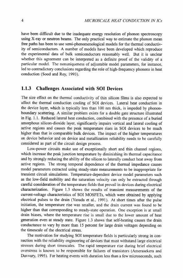
Low-power circuits make use of exceptionally short and thin channel regions, which increase the peak junction temperature by diminishing its thermal capacitance and by strongly reducing the ability of the silicon to laterally conduct heat away from active regions. The strong temporal dependence of the thermal impedance causes model parameters extracted using steady-state measurements to be inappropriate for transient circuit simulations. Temperaturecdependent device model parameters such as the low-field mobility and the saturation velocity can only be extracted through careful consideration of the temperature fields that prevail in devices during electrical characterization. Figure 1.3 shows the results of transient measurements of the current-voltage characteristics of SOl MOSFETs, which were obtained by applying electrical pulses to the drain (Yasuda et aI., 1991). At short times after the pulse initiation, the temperature rise was smaller, and the drain current was found to be higher than that corresponding to steady-state operation. One exception is at small drain biases, where the temperature rise is small due to the lower amount of heat generation even at steady state. Figure 1.3 shows that self-heating causes the drain conductance to vary by more than 15 percent for large drain voltages depending on the timescale of the electrical stress.
The motivation for studying SOl temperature fields is particularly strong in connection with the reliability engineering of devices that must withstand large electrical stresses during short timescales. The rapid temperature rise during brief electrical overstress is known to be responsible for failures of transistors (Amerasekera and Duvvury, 1995). For heating events with duration less than a few microseconds, such

CHAPTER 1. INTRODUCTION 5
5
<" T=290K
E 4 l = 0.46 11m - g,eff 0 0
t- o 0 0
Z 0 • • • • • W 3 • 0::: If 0::: Iil ::::> • 0 2 Z • ~ DATA OF YASUDA et aI., (1991)
C 0 INITIAL
• STEADY STATE
0
0 2 3 4 5
DRAIN VOLTAGE (V)
Figure 1.3: Current-voltage characteristics of a silicon-on-insulator transistor measured under pulsed and steady-state operating conditions.
as in electrostatic discharge (ESD), thermal conduction is confined within a few micrometers of active regions, within which the buried oxide exerts a particularly large impact on thermal conduction cooling. Figure 1.4 plots the failure voltages of SOl transistors subjected to human-body-model (HBM) electrical stresses (Chan, 1995). The HBM emulates the discharge process resulting from physical contact of a chip with a human body. The failure voltage increases with device layer thickness, which reflects the significance of heat conduction along silicon device layers on device temperature rises. The prediction shown in Fig. 1.4 corresponds to the bias voltage that results in a threshold peak temperature (Amerasekera and Duvvury, 1995) as predicted by solving the heat diffusion equation. Brief transient heating can also be very important for SOl power devices. The resulting temperature increase can augment thermal instability among multi-finger bipolar devices, reduce the electrical conductance of field-effect transistors, and reduce the lifetime of devices and metallization.
The analysis and design of SOl devices require accurate property data for constituent materials and thermometry to verify predictions. No experimental data exist for the thermal conductivity of silicon films with thickness of practical importance. Existing thermometry techniques can provide only spatially averaged temperature fields, which are inappropriate especially for SOl power transistors with considerable temperature nonhomogeneity.

6
w ~
c~ wo ~> ..Jw <CO: :IE=> O:..J 0-z~
c en w
o
MICROSCALE HEAT CONDUCTION IN ICs
50
SYMBOLS: CHAN et al. (1995) LINE: PRESENT PREDICTION
100 150
SILICON FILM THICKNESS (nm)
200
Figure 1.4: Experimentally detennined electro-static discharge (ESD) failure voltages of SOl transistors as a function of device layer thickness.
1.1.4 Challenges Associated with New Passivation Materials
Thennal design is of growing importance for interconnect structures in integrated circuits, because their reliability can be strongly influenced by temperature fields. The median time to failure of metallization due to electromigration decreases rapidly with increasing temperature and current density (Black, 1969). This is particularly important for modem integrated circuits incorporating multi-level interconnects. Upper-level interconnects are separated from the substrate by thick passivation layers, which strongly impede thennal conduction cooling. Also important are spatial temperature gradients, which can affect the failure locations and median time to failure. The temperature rise can vary significantly along an interconnect because of nonunifonn heating induced by contacts, comers, and vias.
Interconnects also fail due to brief, high-current pulses encountered during initialization of field-programmable gate arrays (Murguia and Bernstein, 1993; Scarpulla et aI., 1996) and electrostatic discharge (ESD) (Maloney and Khurana, 1985; Banerjee et aI., 1996). The temperature distribution and hence failure locations can vary dramatically depending on the duration of the electrical stress. While the exact failure mechanism is not well understood, melting and delamination of interconnects and the fracture of the surrounding passivation have been considered responsible.

CHAPTER 1. INTRODUCTION 7
Interconnect thermometry is required to investigate the failure mechanisms and to identify possible threshold temperatures and cunent densities for their occunence. One method for measuring the temperature of VLSl interconnects is to monitor their temperature-dependent electrical resistance (e.g. Maloney and Khurana, 1985), which yields the spatially-averaged temperature rise along the interconnects. Several optical methods, including infrared thermography (Kondo and Hinode, 1995), fluorescence thermography (Sakimoto et aI., 1995), and laser-reflectance thermometry (Clayes et aI., 1993) offer the advantage of the ability to spatially map the temperature distribution. Little attention, however, has been paid to thermal mapping of interconnects subjected to brief electrical stresses.
The problem of interconnect thermal failure is becoming more acute with the emergence of a large number of new passivation materials with low dielectric constants, such as porous oxide, and polymers. These new materials are highly disordered and expected to be poor thermal conductors, but their thermal transport properties are not well characterized and understood. A variety of techniques have been developed to determine the thermal conductivity of thin films, especially that in the out-of-plane direction. Reviews of these techniques are available in the literature (Cahill, 1997). Relatively few studies have been devoted to the determination of thermal conductivity anisotropy and volumetric heat capacity of thin films and their process dependence.
1.2 Scope of Research
The present work develops techniques for the thelmal characterization of integrated circuit elements and thin layers of practical importance. A key to these techniques is high spatial and temporal resolution thermometry, which yields transient temperature distributions in integrated circuit elements and thermal property measurement structures.
The primary goal of the measurements of temperature fields in IC elements is to demonstrate quantitative measurements with high temporal and spatial resolution. An optical thermometry technique is developed that utilizes the temperature dependence of reflectance of metal. Particular emphasis has been placed on temperature calibration and possible influence of passivation layers on the calibration coefficients. The major accomplishments in this part of the present work include: construction of a scanning optical reflectance thermometry setup which combines a high power optical microscope with an electrical probe station; development of calibration techniques suitable for integrated circuit elements; and investigation of the effects of duration of electrical stresses and device geometry on temperature distributions in SOl power transistors and interconnects.
The thermometry technique is also applied for the thelmal characterization of thin films. This utilizes the quantitative relationship between the temperature rise in microfabricated measurement structures and the amplitude and frequency of applied harmonic heating. Most previous studies focused only on the thermal conductivity in

8 MICROSCALE HEAT CONDUCTION IN ICs
the out-of-plane direction. Here, high spatial and temporal resolution thermometry techniques allow the determination of thermal conductivity anisotropy and volumetric heat capacity. One of the major accomplishments is to develop the capability to extract both quantities without subjecting samples to disparate and demanding processing steps. The property data for CVD silicon dioxide allow some conclusion to be drawn about the nature of heat conduction in amorphous materials, which is useful in optimizing processing conditions for future passivation layers.
The thin film thermal characterization techniques are extended to the measurements of thermal conductivities of thin crystalline silicon layers. The two primary goals are to help elucidate mechanisms of phonon heat conduction in silicon and to provide data that can be employed in the thermal analysis of SOl devices. The inplane thermal conductivities of mono-crystalline silicon layers as thin as 80 om are obtained for the first time. Scattering of phonons at the film boundaries causes the conductivity to be reduced significantly from the bulk value. The size effect allows indirect measurements of the average mean free path of carriers. A phonon thermal conductivity model is constructed which captures the essential physics but avoids complications arising from a large number of unknown parameters. The model is compared with data obtained from various well-controlled experiments, from which important conclusions about the nature of heat carriers in silicon are deduced.
1.3 Book Overview
Chapter 2 reviews thermometry techniques that have been applied to the thermal characterization of microdevices and thin films. The techniques are divided into two groups, electrical and optical, according to the primary physical quantity measured.
Chapter 3 describes the thermoreflectance technique and related experimental details. Theoretical background is first presented, which includes discussion of various factors that affect the calibration coefficient. This is followed by the description of calibration methods and experimental apparatus. Measurement results are presented on SOl high-voltage transistors and interconnects subjected to brief electrical pulses.
Chapter 4 discusses experimental techniques to determine the out-of-plane thermal conductivity, volumetric heat capacity and the in-plane thermal conductivity of thin films. The thermometry technique described in Chapter 3 forms the basis of these techniques. After presenting background information on thermal conduction in amorphous solids, we discuss experimental results on process-dependent thermal transport properties of silicon dioxide. The implication of these results on the heat conduction mechanism in amorphous solids is discussed.
Chapter 5 presents measurements and analyses of thermal conductivities of thin crystalline silicon films. The chapter begins with theoretical discussion of the phonon spectra in silicon and motivates measurements. The extension of the in-plane thermal conductivity technique of Chapter 4 to single-crystal silicon and its validation are described. The thermal conductivity data are interpreted using a model developed here on the basis of a solution to the phonon Boltzmann transport equation.

Chapter 2
Review of Microscale Thermometry Techniques
There has been considerable progress in recent years in thermometry techniques that characterize microdevices and their constituent materials. Some of these techniques are applicable for both device and material characterization while others are suitable only for device thermometry. This chapter reviews thermometry techniques for microdevices and microstructures. The techniques are categorized depending on whether they employ electrical or optical signals.
2.1 Electrical Methods
Relatively simple experimental setups have made electrical thermometry techniques popular among researchers investigating thermal characteristics of microdevices. Some of the more accurate transport property measurement techniques have also employed electrical thermometry techniques.
2.1.1 Electrical Resistance Thermometry
A thermometry method that lends itself most readily to precise calibration uses patterned bridges made from metals or doped semiconductors. The electrical resistance of the bridge varies with temperature due to the temperature dependence of the electron-phonon scattering rate and, for the case of a semiconducting bridge, also the carrier concentration. The electrical resistance thermometry technique is very attractive for situations where spatial temperature distributions are not important.
One application is interconnect thermometry with the interconnect serving as the thermometer. Maloney and Khurana (1985) and Banerjee et a!. (1996) performed transient electrical-resistance thermometry of interconnects subjected to current pulses of duration less than 1 fJs. Estreich (1989) used gate metals of GaAs

10 MICROSCALE HEAT CONDUCTION IN ICs
metal-semiconductor field-effect transistors (MESFETs) as thermistors to measure steady-state channel temperatures. Mautry and Trager (1990) and also Goodson et al. (1995) adopted a similar technique to study the self-heating of compact fieldeffect transistors (FETs) made of bulk silicon and silicon-on-insulator (SOl) wafers, respectively. Using polysilicon bridges patterned above the active region, Leung et al. (1995, 1997) performed thermometry of the high-power SOl transistors.
Electrical resistance thermometry has also been used extensively for the measurement of thermal transport properties of dielectric and semiconducting materials in microdevices. Steady-state techniques induce louie heating in a patterned bridge and measure resulting temperature rises in the same and nearby bridges to extract thermal conductivity of dielectric layers (Swartz and Pohl, 1987; Orchard-Webb, 1991; Goodson et aI., 1994; Kleiner et al.. 1996). Some transient techniques apply electrical pulses (Okuda and Ohkubo, 1992) or periodically varying currents (Gustafsson et aI., 1984; Cahill, 1990) to a bridge, which serves both as a heater and a thermometer. Chen et al. (1994) heated thin-film samples with a modulated laser beam and detected frequency response of temperature rise in a thin-film resistive sensor. A closely related technique employs microfabricated thermocouple stripes or junctions. This technique also found applications in thermal conductivity measurements (Graebner et aI., 1992; Borca Tasciuc and Chen, 1997).
The principal benefit of patterned electrical-resistance thermometers is that they can be precisely calibrated, which enables accurate thermal characterization of devices and material properties. This approach, however, has several limitations: 1) The thermometer provides only spatially-averaged temperature along a patterned bridge at a single location. High spatial resolution can be achieved only in one dimension, and temperature distributions cannot be readily captured. 2) In the thermometry of microdevices, capacitive coupling between the circuits and reflection of voltage signals within the circuit limit the temporal resolution to a few hundred nanoseconds. 3) Devices often need to be modified in a nontrivial way.
2.1.2 Scanning Thermal Microscopy
The invention of the scanning tunneling microscope (STM) and the atomic force microscope (AFM) have made possible unprecedented spatial resolution in surface characterization. Among them are techniques to interrogate temperature or thermal properties. The scanning thermal profiler of Williams and Wickramasinghe (1986) uses heat transfer as a feedback mechanism for the tip-sample separation. Variations in the thermal properties of samples were qualitatively mapped by Nonnenmacher and Wickramasinghe (1992) using a heated scanning STM probe and by Maywald et al. (1994) using a heated AFM probe. Majumdar et al. (1993) replaced the cantilever in an AFM with thermocouple wires whose junction formed a scanning probe tip. Luo et al. (1996) developed a new fabrication technology that yields thennocouple junctions of dimensions comparable to 100 nm near the tip of a silicon nitride cantilever probe and captured temperature distributions in a semiconductor laser (Luo et aI., 1997).

CHAPTER 2. REVIEW OF THERMOMETRY TECHNIQUES 11
Scanning probe microscopy has the potential to provide the best spatial resolution for microdevices. There are important drawbacks with this approach: 1) The tipsurface thermal conductance is influenced by topographical features, such that the tipsurface temperature drop may vary during a scan. This leads to spurious information in the shape of measured temperature profiles. Topographical features also result in an increase in the effective size of the temperature sensing region and degrade spatial resolution. 2) The temperature drop between the scanning tip and the surface is difficult to determine precisely, such that the magnitude of temperature rise cannot usually be determined with low uncertainty. 3) Capacitive coupling between the probe and a device under test obscures temperature signals at short timescales.
2.1.3 Thermometry Using Temperature Sensitive Electrical Parameters
The electrical behavior of a transistor and its component junctions can be strongly influenced by temperature. This makes possible thermometry of a transistor with little or no modification. The sensitivity for thermometry can be greatest for diodes within semiconductor devices, such as the base/emitter diode in a bipolar transistor and the drain/channel or source/channel diodes in field-effect transistors (Blackburn, 1988; Cain et aI., 1992). Zweidinger et aI. (1996) proposed a systematic approach to extract the thermal impedance of bipolar transistors based on temperature sensitive electrical parameters (TSEP's).
The pre-selected TSEP is first calibrated using an external temperature controller. During the calibration step, the heat generation inside the device should induce a negligible temperature rise. During the measurement, the device is heated using an electrical current of magnitude typical during operation. The device operation is interrupted briefly, and the TSEP is monitored using the lower calibration current. Junction temperatures in high-frequency power transistors were measured by Cain et al. (1992) using the base-emitter voltage as a TSEP. Liu and Yuksel (1995) used the tum-on voltage of AlGaAs/GaAs bipolar transistors under given collector current for thermometry. Arnold et aI. (1994) used the low-current drain-source voltage across SOl power transistors to determine the transient temperature rise. The drain conductance served as a TSEP in the study of self-heating effects in SOl MOSFET's (Tenbroek et aI., 1996).
The major advantage of TSEP thermometry is that it can be performed on fully packaged devices with little or no modification. The temperature is measured directly within the transistor rather than at the surface of a sample, which is the case for the scanning thermal microscopy and most of the optical methods. This can be important when there are thick passivation layers separating active regions from the surface. But there are major drawbacks associated with TSEP thermometry: 1) The thermometry provides only a weighted-average value of temperature in a device. 2) The calibration is carried out under isothermal condition, which does not reflect nonuniform temperature distribution in the device under operating conditions. 3) The low-power calibration condition cannot be established in the transistor with

12 MICROSCALE HEAT CONDUCTION IN ICs
arbitrary speed due to switching transients. This leads to temporal delay between the termination of normal operation conditions and the thermometry that can be comparable to or larger than 1 J1S. The device cooling can be significant during this period.
2.1.4 Noise Thermometry
The rate of current flow through an electrical resistor experiences statistical fluctuations at a finite temperature, which induces thermal voltage noise. The thermal voltage noise associated with a resistance R is given by (4kB TRtlf)1/2, where tlf is the frequency bandwidth under consideration. Measurement of the thermal voltage noise of a resistor can thus yield its temperature. Bunyan et al. (1992) fabricated a doped polysilicon resistor normal to the direction of a current flow in a SOl MOSFET and within the plane of the substrate. The noise associated with this resistor was monitored during operation of the transistor, providing data for the steady-state channel temperature. The noise thermometry technique requires special device structures and can only provide average temperature information.
2.2 Optical Methods
Every solid exhibits temperature dependence of its optical properties, which can form a basis for various optical thermometry techniques. Some methods use radiation interaction with the surface of a metal, semiconductor or other special thin layer, such as liquid crystal. In other cases transmission of radiation through a dielectric or semiconducting layer is probed. Optical methods provide spatial temperature distributions and have the potential to achieve high temporal resolution by not contributing to the thermal mass or the electrical capacitance of the system. Some optical methods do not require physical contact with the sample, eliminating the possibility of spurious influences of a probe on the temperature field.
2.2.1 Thermoreflectance Technique
Thermoreflectance thermometry detects temperature changes near a surface using the dependence of the optical reflectance on temperature (Cardona, 1969). Relative change in the optical reflectance per unit temperature change is termed the thermoreflectance coefficient. The thermoreflectance coefficient varies strongly with material and probe beam wavelength, and its typical magnitudes range from 10-6 to 10-4
for metals and semiconductors. The thermoreflectance technique is promising for rapid thermal mapping of microdevices. A temporal resolution better than 1 ns has already been demonstrated on flat metal surfaces heated with picosecond laser pulses (Eeseley, 1983). The temporal resolution is ultimately limited to the order of the relaxation times associated with the microscopic scattering processes governing the reflectance, which is typically of the order of picoseconds in metals. Also promising

CHAPTER 2. REVIEW OF THERMOMETRY TECHNIQUES l3
is the opportunity to use radiation wavelengths for which most passivation layers are transparent. The spatial resolution of this technique is limited by the diffraction of the probe beam and can be comparable to the wavelength of the beam. Further details of the technique will be provided in Ch. 3.
The technique is most readily applied to metal interconnects, whose temperature fields were captured in near steady-state (Claeys et aI., 1993). The small radiation penetration depth in metals allows a precisely defined measurement location. Temperature rises in semiconductor regions were also captured. Epperlein (1993) and Mansanares et al. (1994) studied the impact of temperature fields on the failure of semiconductor lasers, and Abid et al. (1996) captured temperature distributions in large-area power transistors.
The thermoreflectance technique has also been applied for the extraction of thermal properties of thin films. Thermal transport in metal films was investigated (Clemens et aI., 1988; Mikl6s and Lorincz,1989) by monitoring the shape of the temperature decay after the termination of a short-duration heating laser pulse. A similar technique has been used to extract the thermal conductivity of dielectric materials (Fanton et aI., 1989; Kading et al., 1994; Capinski and Maris,1996).
The disadvantages of the technique are: I) Interaction of incident radiation with active regions of semiconductor devices can int1uence the device operation and complicate the extraction of temperature through electro-optical effects. 2) Calibration is complicated by the presence of different materials and topography.
2.2.2 Thermal Expansion Thermometry
Thermal expansion of solids can be measured with high precision using optical interferometry or scanning probe microscopy, which provides information on local temperature. Martin and Wickramasinghe (1987) studied current distributions in microcircuits using this principle. Claeys et al. (1993) measured the dilatation at the surface of an electrically biased FET using a similar approach. Majumdar and Varesi (1997) used an atomic force microscope instead of an optical interferometer to measure thermal expansion. Since thermal expansion is a function of the temperature field throughout the device and neighboring substrate, local temperature information is difficult to obtain. The problem is more acute for semiconductor devices, which consist of mu1tilayers with vastly differing thermal expansion coefficients.
2.2.3 Micro Raman Spectroscopy
Raman spectroscopy examines inelastic photon-phonon scattering processes in a crystal. The scattering of the incident photons by phonons in a crystal leads to shift in energies of the outscattered photons and the creation or annihilation of an optical phonon. The probability of the inelastic scattering is temperature-dependent and is related to the occupation number of optical phonons. Micro Raman spectroscopy uses highly focused laser light to perform thermometry with resolution better than

14 MICROSCALE HEAT CONDUCTION IN ICs
1 p,m. Ostermeir et aI. (1992) employed the Raman technique to acquire temperature distributions in silicon MOSFETs. Brugger and Epperlein (1990) determined the surface temperature profile in quantum well lasers, which correlated well with laser degradation. The drawbacks associated with this technique include the unknown influence of incident radiation on the device behavior and ill-defined vertical measurement locations due to the finite radiation penetration depth. Relatively complicated and time-consuming measurement procedure makes transient measurements very difficult.
2.2.4 Photothermal Deflection Method
The temperature-dependence of the index of refraction of a material can be monitored through the deflection of a transmitted beam. A refractive index gradient formed in the gas layer adjacent to a heated sample surface alters the propagation direction of a beam, a phenomenon generally called the mirage effect (Boccara et aI., 1980). Detection of beam deflection yields information on the surface temperature, which can be subsequently used to extract thermal properties of solids. Deboy et aI. (1996) applied a similar method to solids and measured the average temperature along a laser beam path through semiconductor devices. The average device temperature was deduced using independent data for the temperature dependence of the index of refraction and carrier-induced absorption. Problems with this approach include the arduous sample preparation process, which is required to provide optical access to both sides of the device, and the difficulty of performing a precise calibration. This technique is poorly suited for interrogation of active regions of devices because of the impact of photogeneration on device operation and electro-optical effects.
2.2.5 Liquid Crystal Thermometry
Liquid crystal thermometry has been available for more than two decades (e.g., Caroll, 1973; Meier et aI.,1975) and has been used predominantly for the qualitative detection of hotspots in integrated circuits (Beck, 1986). Some liquid crystals operate at temperatures up to a few hundred degrees. Significant efforts are required if quantitative temperature information is needed.
Liquid crystals have been used for thermometry in the cholesteric phase by exploiting temperature dependence of their color. Fergason (1968) discussed the possibility of a spatial resolution of 25 p,m and temperature resolution of 0.1 K using this approach. A second approach is to utilize the transition of crystals between the nematic and the isotropic phases (Stephens and Sinnadurai, 1974). The nematic phase changes the polarization state of light reflected from it, while the isotropic phase does not. Polarization optics allows regions coated with the nematic and isotropic crystals to be distinguished with spatial resolution of a few micrometers (Aszodi et aI., 1981). The use of nematic/isotropic phase transition, however, suffers from the drawback that only one isotherm can be obtained each time. Active control

CHAPTER 2. REVIEW OF THERMOMETRY TECHNIQUES 15
of environmental temperature to get multiple isothenns was suggested to circumvent this difficulty (Stephen and Sinnadurai, 1974).
2.2.6 Infrared (IR) Thermometry
Infrared thennometry technique utilizes the fact that electromagnetic radiation emitted from a solid can be correlated to its temperature. By measuring the spectral distribution of emitted radiation or total emitted power, the temperature of a solid can be detennined. This process requires calibration of the emissivity, which varies with materials, surface conditions, and wavelengths (Bennett and Briles, 1989). The spatial resolution is limited by diffraction to the order of the interrogated wavelength. The wavelength at which the blackbody radiation peaks is near 10 /-Lm at room temperature, a resolution which renders IR thennography appropriate for qualitative thermal mapping over relatively large regions of an integrated circuit. One interesting application is demonstrated by Kondo and Hinode (1995), who employed IR thermometry to study the long timescale failure of interconnect structures. Recently Feng et al. (1996) and Boudreau et aI. (1997) made use of tapered optical fibers with aperture size of the order of a micrometer to improve the spatial resolution. The implementation suffered from difficulties associated with calibration and strong thermal emission from a metal coating, which was necessary to reduce the aperture size.
The thermal diffusivity of a thin film was measured by heating the sample surface with a pulsed laser and monitoring the decay in surface temperature by means of IR thennometry (de Jesus and Imhof, 1995). Graebner (1995) produced a transient thermal grating and observed its time evolution using an infrared detector to obtain thennal diffusivity of thin films in the in-plane direction.
2.2.7 Photoluminescence Thermometry
Photoluminescence (PL) occurs when a system makes transition to a higher energy level by absorbing a photon and then spontaneously decays to a lower energy level, emitting a photon in the process. The photoluminescence spectra is wavelength and temperature dependent, enabling the interrogation of temperature fields. Hall et aI. (1992) obtained temperature profiles in a diode laser by monitoring the peak wavelength of the PL spectrum, which varies roughly linearly with temperature. Similar measurements were conducted on pseudomorphic high-electron-mobility transistors (Landesman et aI., 1998), whose operating temperature was deduced from the shift in wavelength of the PL peak. Since carrier concentration, surface band-bending, other effects can contribute to a band-gap shift and hence the PL spectrum, (Hall et aI., 1992), direct application of the PL thennometry over the active regions of devices requires extra care.
Another approach, tenned fluorescence thennometry, uses the temperature dependence of the fluorescence quantum efficiency of thin-film coatings. One commonly used coating contains europium thenoyltrifluoroacetonate (EuTTA) (Kolodner and

16 MICROSCALE HEAT CONDUCTiON IN ICs
Tyson, 1982), which emits visible light at around 612 run when irradiated by ultraviolet radiation (340-380 run). The intensity of stimulated fluorescence varies exponentially with the film temperature. Temperature fields in a device can be extracted by measuring the fluorescence intensities with and without electrical bias and subsequently comparing the two intensities. Kolodner and Tyson (1983) demonstrated a spatial resolution of 0.7 /Lm. The temporal resolution has not been investigated, although the fluorescence decay time of around 200 ILS is measured for EuTTA. Disadvantages of this technique include the practical difficulties associated with sample preparation, the degradation in the fluorescence properties of the EuTTA films during lengthy exposure to the UV radiation, and the effect of film dilution on sensitivity (Barton and Tangyunyong, 1996).

Chapter 3
High Spatial and Temporal Resolution Thermometry
The preceding chapter provides an overview of theni10metry techniques applicable for microdevices and microstructures. The present research realizes the potential for high temporal and spatial resolution of the thennoreflectance technique thennoreflectance technique by developing an experimental setup that combines diffraction limited optics with a high speed electrical probing facility. Quantitative as opposed to qualitative temperature distributions can be obtained using calibration methods developed in the present study. The setup is employed for the thennal characterization of microdevices subjected to brief electrical stresses and for the detennination of thennal transport properties of thin films. The present chapter provides details of the technique and its application for microdevices. Subsequent chapters describe thennal characterization of thin films.
3.1 Thermoreflectance Thermometry Technique
The first part of the section discusses in detail the thennoreflectance phenomenon. Special emphasis is placed on those aspects that are closely related to the high temporal and spatial resolution thennometry of microstructures and microdevices. This is followed by a discussion of a newly developed calibration method, which is essential for quantitative temperature measurements.
3.1.1 Thermomodulation Spectra
The degree to which the optical reflectance varies with temperature detennines the sensitivity of the thennoreflectance technique. A quantitative measure of this variation is called the thennoreflectance coefficient thennoreflectance coefficient, CT R,

18 MICROSCALE HEAT CONDUCTION IN ICs
which is defined as the relative change in the reflectance per unit change in temperature. For metals the magnitude of CT R is typically close to or less than 10-5 K -I,
resulting in sensitivity two orders of magnitude lower than that of the electrical resistance thermometry. At certain wavelengths, however, the thermoreflectance coefficient assumes considerably larger values, which can be exploited to improve signal-to-noise ratio. The understanding of thermomodulation spectra is also important in assessing the transferability of the calibration parameter from one type of film to another.
The optical reflectance of a metal film varies with temperature due to a number of different mechanisms (Rosei and Lynch, 1972): 1) Volumetric thermal expansion alters interatomic separations leading to modifications in the electron energy bands and plasma frequencies. 2) Shear strains are induced when the film is constrained by the substrate, leading to the splitting of degenerate bands and other modifications in the energy bands. 3) The Fermi-Dirac distribution is a function of temperature. Transitions involving states near the Fermi level are therefore influenced by the film temperature. 4) The population of phonons increases with increasing temperature, which raises the rates of electron relaxation through phonon - electron interactions.
Figure 3.1 shows the optical reflectance of evaporated aluminum films and its temperature derivative as functions of the wavelength (Decker and Hodgkin, 1981). At a wavelength near 800 nm a pronounced minimum in the reflectance is observed. This feature has been attributed to interband transitions between free electron-like bands in aluminum, which are partially filled with electrons (Ehrenreich and Philipp, 1963). The resonant absorption responsible for the dip is strongly influenced by detailed configurations of the energy bands, which themselves are affected by the film temperature. As a result, the temperature derivative of the reflectance varies rapidly with wavelength at around 800 nm. For copper a similar feature in the temperature derivative has been observed at the wavelength of 577 nm (Rosei and Lynch, 1972). In the long-wavelength limit, the temperature dependence of the reflectance is due primarily to electron-phonon scattering. The temperature derivative of the optical reflectance approaches a constant value, which can be predicted from a modified free-electron Drude model accounting for phonon-electron interactions.
Although spectra obtained in other studies share many of the key features illustrated in Fig. 3.1, differences among the measured spectra do exist. For instance, the thermoreflectance data of Rosei and Lynch (1972) completely lack the prominent minimum at the wavelength near 111m and make smooth transition from the peak at around 800 nm to the flat region in the long-wavelength limit. Quantitative comparison between the measured spectra is difficult because very few previous studies obtained absolute values of the temperature derivative of the reflectance.
The discrepancy among the measured thermomodulation spectra is not unexpected in view of the various mechanisms responsible for the thermoreflectance phenomenon. Film thickness and film-substrate adhesion are some of the factors influencing shear strain as well as volumetric thermal expansion of the film. Extrinsic electron scattering sources such as lattice defects and microtopographical structures at film surfaces can also modify the spectra (Rosei and Lynch, 1981). The latter fact

CHAPTER 3. HIGH RESOLUTION THERMOMETRY 19
15 • • • • 10 • • • ------+ 0.9
~ ~. ::tJ
~ m
" .... 5 • 0.8 r 0 m ..... • (")
• -t t- O » "0 0.7 Z ~ +-- • • • • (") "0 • m
-5 0.6
• • -10 • DECKER and HODGKIN (1981)
0.5 0.6 0.8 2 3
WAVELENGTH (Jlm)
Figure 3.1: Spectral dependence of the reflectance and its temperature derivative for evaporated aluminum (Decker and Hodgkin, 1981).
has an implication in the thermometry of integrated circuit elements since metal films in these devices are often alloys with varying compositions and grain structures.
3.1.2 Impact of Dielectric Overlayers
The thermoreflectance signal is also affected by the presence of dielectric overlayers dielectric overlayer with thickness of the order of the wavelength of a probe beam, a situation commonly encountered in integrated circuits. Interference among multiplyreflected beams alters the optical reflectance and influences the thermoreflectance signal in a manner that is sensitive to its thickness, the wavelength of the probe beam, and the optical properties of both the overlayer and the base material. The presence of a silicon-dioxide layer has been observed to alter the surface reflectance of silicon and its temperature dependence (e.g., Friedrich et ai., 1991; Quintard et aI., 1996). The present study uses the theory of thin-film optics (Siegel and Howell, 1992) to predict the impact of passivation layers and to draw conclusions about the resulting uncertainty in the thermoreflectance thennometry of underlying opaque layers.
For normal incidence, the surface reflectance, R, is related to the indices of refraction, iibase and nm'er and the thickness of the overlayer, L, in the following

20 MICROSCALE HEAT CONDUCTION IN ICs
way:
R = I rl + r2 exp( -i~7rn01,erL/ ,X) 1'2 11 + rlr2exp(-z47rnO'l,erL /,X)
The amplitude reflection coefficients rl and r2 are
nair - n01.1er rl = -----
nair + nO'l'er nO'l'er - ii'b(lse
T2 = _ T1'{Yl)(~r + nblLSC
(3.1)
(3.2)
The dielectric over layer is assumed to be transparent at the probe beam wavelength. The thermoreflectance coefficient, GT R, is expressed as
1 dR GTR = RdT (3.3)
Equations (3.1) and (3.2) are applied to silicon samples capped with silicondioxide layers. Silicon is chosen since its optical properties are very well characterized over large temperature and wavelength ranges and hence the comparison of the prediction with the data is most meaningful. Abid et al. (1996) reported the thermoreflectance coefficients of silicon samples for several different probe beam wavelengths. The experimental data of Jellison and Modine (l982a,b) and Jellison and Burke (1986) are used for the optical properties of silicon in the calculations. The index of refraction of silicon dioxide is assumed to be 1.46. Figure 3.2 compares the experimental data with the predictions for two different thicknesses of the silicon-dioxide overlayers. While the thermoreflectance coefficient of silicon is nearly constant over the wavelength range examined, the oxidized silicon samples exhibit significant variations in GTR . The predictions agree reasonably well with the data except near the wavelength of 500 nm. The discrepancy can result from several different sources, including the uncertainties in the indices of refraction of silicon and silicon dioxide, as well as the uncertainty in the thickness of the overlayer. Also important is the temperature dependence of the index of refraction of the overlying silicon-dioxide layer, which is not taken into account.
In principle, similar calculations can be performed for a metal base material, such as aluminum. In many cases, however, the index of refraction as a function of temperature is unavailable for thin metal films. Considerable uncertainties in the index of refraction can present serious obstacles to reliable predictions. A knowledge of the thermoreflectance coefficient of an unpassivated metal layer alone is insufficient to uniquely determine the temperature derivative of the real and imaginary parts of the index of refraction, nT and kT, respectively, which are necessary for the present calculation. Only a rough estimate can be made via a parametric study conducted on a sample without an overlayer. The present study assumes a complex refractive index of the form (Smith et al.,1985)
ii'AI = (2.75 + nT,AID.T) - i(8.31 + kT,AID.T). (3.4)

CHAPTER 3. HIGH RESOLUTION THERMOMETRY
..,: z w o u. u. w o o w 0 .... -Z ~
~ o W ...J U. W ~ o ~ ~ W ::I: ....
II:: I-
o
6104 ~--------------------------------~ SYMBOLS : DATA (ABID et aI., 1996) THICK LINES PREDICTIONS
L = 1520 nm ()r". Si02 lO , ...
.' ,'J ',\
" 0'
. , , \
f~" " n = 1.46
Si02
0100 ~--------------------------------~ 450 500
WAVELENGTH (nm)
21
Figure 3.2: Wavelength dependence of the thermoreflectance coefficient of silicon with silicon-dioxide overlayers. The predictions take into account the interference among multiply-reflected beams.
For each value of '/1T, the corresponding value of K:y is obtained by matching the predicted eTR to the measured value. Plotted in Fig. 3.3 is the predicted thermoreflectance coefficient of an aluminum sample covered with a 111m-thick silicondioxide layer. The aluminum layer is assumed to be opaque and the index of refraction of silicon dioxide is assumed to be constant at the value of 1.46. The calibration results for aluminum films, which are to be discussed in the next section, are included for reference.
The foregoing calculation is based on a parallel beam assumption where the crosssectional area of the probe beam remains constant as the beam propagates through the overlayer. To achieve high spatial resolution, however, a focused Gaussian beam is most often employed, whose diameter varies due to diffraction as the beam travels through a medium. In this case, the spatial regions occupied by the multiply reflected beams do not exactly coincide with each other, which can influence interference among them and thereby the thermoreflectance coefficient.
In the present study the probe beam is focused and recollected using the same optical elements. In this so-called confocal optical configuration the majority of the collected beam comes from those portions of the multiply reflected beams that spatially overlap the beam waist. Estimates of the impact of the beam diffraction on the thermoreflectance coefficient are made for this situation. The following

22 MICROSCALE HEAT CONDUCTION IN ICs
I-Z W 15 (3 i..= 825"m u:: LL W 0 WITH OVERLAYER 0 10 W ... ~ 0 Z III c:( 0 .... I- - NO OVERLAYER 0 II: W I- 5 ..J 0 L= 1~m LL
"AI = 2.75 + "T.AI AT W r:t:: k AI = 8.31 + kT•AI AT "Si02 = 1.46 0 ~ 0 r:t::
-5 10-3 010° 510-3 W :I: l- n (K-1)
T,AI
Figure 3.3: Impact of uncertainties in the temperature-dependence of the index ofrefraction of aluminum on the predicted thermoreflectance coefficient of an aluminum layer with an 1 /-Lm-thick silicon-dioxide overlayer. The calibration results marked with arrows are only for reference.
simplifying assumptions are made: 1) The beam radius 11' is assumed to vary with distance from the waist z according to
w(z) ~ Wo [1+ (~~~ rt', (3.5)
where Wo is the beam radius at the waist. 2) The beam has a Gaussian intensity distribution with cut-off at the beam radius. 3) Only those portions of the multiply reflected beams are collected which are contained within a circle of radius 111 (L) located at the surface of the overlayer. Under these assumptions the reflectance is calculated to be
{ weLl R* R d R = vO M Mr ,r
{ "v(L) (2 2/ (L)2) d . , () e.Tp - r 111 r r (3.6)
The term RM is obtained by modifying a corresponding expression for the parallel beam case:

CHAPTER 3. HIGH RESOLUTION THERMOMETRY
..,: z w (3 LL. LL. W 0 (J
w ..... ~ (J z "6 « -I- -(J 0:: W I-
...J (J
LL. W 0::: 0 ::iE 0::: W ::I: I-
12
11 A. = 825 nm
L = 111m
n = k = -4.6x10⁻³ T T
GAUSSIAN BEAM PARALLEL BEAM
n = -1.5x1 0-3 k = -4x1 0-4 T ' T
10 ~------------------------------~ 2 3
BEAM WAIST RADIUS ~m)
23
Figure 3.4: Approximate calculation of the impact of the beam size on the thermoreflectance coefficient of a passivated aluminum layer.
Figure 3.4 shows the predicted GTR of an aluminum layer with a 111m-thick silicon-dioxide overlayer. A highly focused Gaussian beam can lead to noticeable deviation in the therrnoreflectance coefficient from the parallel beam results. The deviation is sensitive to the temperature derivative of the index of refraction of aluminum, which is not precisely known, and diminishes with increasing beam waist radius. The two particular sets of values of ny and ky are obtained from the parametric study discussed earlier. Similar behavior is observed for other combinations of nT and kT . It can be concluded that a calibration performed using a certain optical configuration may not be transferable to other optical configurations.
3.1.3 Calibration
An accurate calibration method is an essential element of any quantitative thermometry techniques. This is of particular importance for the thermometry of integrated circuit elements, whose constituent materials have optical properties that are not well-characterized or can vary depending on the processing details (e.g., Pliskin, 1977). Theoretical predictions of the thermoreflectance coefficient C TR are hampered by difficulties outlined in the preceding subsections. Very few data exist for the absolute values of GT R in the literature. Two different calibration methods

24 MICROSCALE HEAT CONDUCTION IN ICs
for thennoreflectance coefficients can be used, one using an external temperature controller and the other employing microfabricated structures.
In the fIrst method, the temperature of a sample is controlled externally while variations in its reflectance are measured. This approach has the advantage of a relatively simple experimental setup and procedure. However, this method is difficult to apply for optical systems with a large numerical aperture and a shallow focal depth, which is needed to achieve high spatial resolution, because thermal expansion of a sample - heater assembly can lead to errors. Although this problem can be avoided by preparing a dedicated calibration sample with a large surface area and by using a separate optical system for calibration, the dependence of the thennoreflectance coefficient on the beam waist radius should be properly taken into account.
The second method induces localized heating, which strongly diminishes the thennally-induced deflection of the surface. An example of this approach is to lithographically pattern the metal fIlm of interest into a bridge structure and use it both as a heater and as a thermometer. The temperature dependence of the electrical resistance of the metal line is determined separately. The thennoreflectance coefficient is obtained by comparing the changes in the surface reflectance with those in the electrical resistance while subjecting the stripe to periodically varying currents.
While the application of the electrical resistance thermometry is quite straightforward under steady-state conditions, corresponding measurements under transient conditions require a somewhat sophisticated approach. When a metal line is subjected to harmonic Joule heating, the resulting temperature rise can be extracted from the third harmonic component of voltage oscillations across the line (Cahill, 1990). Figure 3.5 illustrates the underlying principle of the 3w technique. Consider a sinusoidally varying current I = 10 sin(wt) that passes through a metal stripe with electrical resistance Re. The temperature in the stripe exhibits oscillations at twice the current frequency since Joule heating is insensitive to direction of current flow. The temperature oscillation is reflected in the corresponding variations in the electrical resistance according to
Re = Re,o + 6.Re(6.T) sin(2wt), (3.8)
where R",o is the steady-state value of the electrical resistance. In the case of metal fIlms commonly encountered in microdevices and microstructures, 6.R" is linearly proportional to 6.T near room temperature and above. The material-dependent proportionality constant is referred to as the temperature coefficient of resistance (TCR). When combined with the current oscillation at the angular frequency w, 6.Re gives rise to a third-harmonic component in the voltage drop across the metal bridge, whose magnitude 6. V3w can be expressed as
(3.9)
Knowledge of dR/ dT would then enable the temperature oscillation to be deduced from the measured 6. V3w.

CHAPTER 3. HIGH RESOLUTION THERMOMETRY
CURRENT AT 00
TEMPERATURE AT 200
RESISTANCE
VOLTAGE AT 00 AND 300
300 COMPONENT
Figure 3.5: Schematic illustration of the 3..; thermometry technique.
3.1.4 Experimental Apparatus
25
The present study develops the experimental facility shown in Fig. 3.6, which integrates scanning laser diagnostics and electrical probing and thus allows simultaneous investigation of thermal and electrical behavior of microdevices. A laser diode system with a single-element glass aspheric focusing lens and astigmatic correction optics is used. The output beam from the diode laser system has a Gaussian intensity profile with the beam divergence angle of 0.14 mrad. Radiation from the laser diode system is coupled into an optical microscope and focused to a diameter near the wavelength using microscope objective lenses with numerical aperture as high as 0.9. The wavelength of the laser diode used in the present study is 825 nm. Laser power fluctuations are subtracted using a reference beam drawn by a beam splitter. The radiation powers are captured using photodiodes with 500 MHz bandwidth and a digital oscilloscope with 1 GHz sampling frequency. The temporal resolution achievable in this setup is near IOns and the spatial resolution is limited by the diffraction of a probe beam to the order of its wavelength.
The probe laser focus is scanned over the wafer surface using a pair of galvanometrically-actuated mirrors that rotate about orthogonal axes while the semiconductor device and the electrical probes remain stationary. This feature allows the use of standard microprobes, facilitating wafer-level device characterization. A schematic diagram of the scanning system is shown in Fig. 3.7. A polarization cube and a

26 MICROSCALE HEAT CONDUCTION IN ICs
')J4 BEAM SCANNING PLATE SPLITTER
MIRROR PAIR/) ---~--~~--tiwmll
OPTICAL MICROSCOPE
MICROPOSITION ER
</~ LASER
SAMPLE
Figure 3.6: Schematic of the scanning laser-reflectance thermometry facility developed in the present study. A probe laser beam is focused down to the diffraction limit by an optical microscope and scanned over a sample surface using a pair of scanning mirrors.
quarter-wave plate separate the incident and reflected probe beam paths. The current setup allows the direct observation of sample surfaces during measurements either through an eyepiece or a CCD camera.
3.2 Thermal Characterization of Silicon-on-Insulator High-Voltage Transistors
The thermoreflectance thermometry technique is applied to silicon-on-insulator (SOl) power transistors, which are designed to block high-voltages in power circuitry. A schematic diagram of the transistor structure used in the experiments is shown in Fig. 3.8. The drift region is 40 J.lm long and 2 mm wide. To assist with the thermometry, an aluminum layer is sputtered within the surface oxide. The thickness of the aluminum layer is 25 nm, which is larger than the optical penetration depth of 8 nm at the probe beam wavelength 825 nm. It therefore strongly reduces interaction between the radiation and the transistor and precisely defines the vertical location at which temperature is measured. But the presence of the aluminum and its separation

CHAPTER 3. HIGH RESOLUTION THERMOMETRY
MICROSCOPE OBJECTIVE ............ _ .....
FOCUSING LENS
SCANNING MIRRORS
27
Figure 3.7: Schematic diagram of the probe beam scanning system. A pair of galvanometrically actuated mirrors steer the probe beam, whose trajectories are shown as dotted lines.
from the drift region limits the spatial and temporal resolution of the measurements. To reduce the total thickness of the silicon dioxide layer, part of the thermally-grown silicon-dioxide layer is etched away before the deposition of a CVD oxide layer. The importance of lateral heat conduction within the aluminum layer can be estimated by using the thermal decay length (Shirley, 1985), LD = (kadado/ ko)1 / 2, where ka and da are the aluminum thermal conductivity and thickness respectively, and ko and do are the thermal conductivity and thickness of the oxide separating the aluminum from the device. The estimated thermal decay length is 1 11m, resulting in a spatial resolution limit that is important but not significantly more restrictive than that due to the diffraction of the incident probe laser beam. The spatial resolution limit due to heat spreading within the silicon-dioxide layer is comparable to its thickness, 0.6 p,m. The silicon-dioxide passivation also places limitation on the temporal resolution, which is approximately given by the time required for heat to diffuse normal to the layer, tD = L~/ 0o, where Lo is the thickness of the oxide passivation layer and 0 0
is the thermal diffusivity of the silicon-dioxide layer. The thermal diffusion time is around 0.5 11S for the transistors studied here. These practical limitations on the resolution can be removed for the thermometry of interconnects and metallized regions of microdevices, which do not require any structure modifications.

28 MICROSCALE HEAT CONDUCTION IN ICs
/ SOU RCE "'---/ GATE \'-_______ ---1/ DRAIN
/ ' \.J-.-\ SILICON DIOXIDE, 1 Ilm /
" -OXIDE ALUMINUM, 25 nm SILICON
/ DRIFT REGION , 0.2 Ilm THICK
BURIED SILICON DIOXIDE, 2 OR 3 Ilm THICK
SILICON SUBSTRATE
Figure 3.8: Cross sectional view of the silicon-on-insulator high-voltage transistor used in the present thennometry study. A thin aluminum layer is deposited between the silicon dioxide passivation, which prevents radiation interaction with the transistor and sharply defines the vertical position of the temperature measurement.
During the thennometry, repetitive voltage pulses of duration near 30 lIS and magnitude near 30 V are applied to the drain. The duration of the pulse is chosen such that the influence of the buried oxide layer on the temperature rise can be examined over a broad timescale. The duty cycle of the pulses is less than 0.01 to ensure complete cooling of the devices between successive heating pulses. The gate of the transistor is positively biased at 12 V and the source is grounded. At each scan point, the periodic temperature rise is acquired as a function of time after pulse initiation. Once these data are obtained for the entire sample surface, the spatial temperature-rise map can be extracted at any time.
The probe beam power is less than 1 m W. The temperature rise due to the probe laser is estimated to be small since the conduction cooling through the substrate, which is augmented by the lateral spreading of heat in the metal film, is substantial. For absorbed laser power as high as 0.1 m W, the estimated laser-induced temperature rise in the aluminum layer is less than 10K. Since the present technique measures changes in temperature rather than its absolute magnitude, the steady-state temperature field does not directly influence the measurements. When the laser-induced heating is significant, however, it can alter device characteristics and thereby indirectly affect the results. The impact of laser heating on the measurements is examined

CHAPTER 3. HIGH RESOLUTION THERlI,fOA1ETRY 29
experimentally by varying the incident probe beam power and also the focused beam spot size. There are no observable variations in the measured temperature rises as well as in the electrical characteristics of the devices.
The calibration for the transistor structures is performed using the first of the two methods described in Sec. 3.1.3. The silicon wafer containing the transistors is fixed by means of air suction to a temperature-controllable hot-chuck made of copper. The changes in the surface reflectance are monitored while inducing periodic variations in the wafer temperature. The area of the transistor region, over which the aluminum layer is deposited, is large enough to allow the use of an optical system with a large depth of focus. This avoids error resulting from the thermal expansion of the calibration system. To verify the calibration, a control wafer is prepared which has an aluminum layer deposited over the entire wafer. By eliminating the need for focusing optics, the impact of the thermal expansion on the calibration system is minimized. The two calibration results agree well within the uncertainty limit.
Section 3.1.2 shows that the probe beam size can influence the thermoreflectance coefficient when a dielectric overlayer is present. The applicability of the calibration coefficient obtained using a large area probe beam to the high-resolution thermometry needs to be assessed. To this end, a transistor structure similar to the one shown in Fig. 3.8 is fabricated, whose drift region is uniformly doped. This results in a homogeneous temperature field over a large portion of the drift region. Temperature measurements are performed using microscope objective lenses with numerical apertures of 0.1, 0.2, and 0.5, while subjecting the structure to identical electrical stressing conditions. The results obtained using the three lenses with different beam waist sizes vary by less than 5 percent.
A major source of noise in the current setup is the diode laser, which is sensitive to the back reflection and the environmental conditions. The photo-detector and signal amplifier contribute additional noise. The relative uncertainty in the absolute value of the measured temperature rise is dominated by that in the calibration coefficient, CT R, which is estimated to be 10 percent. Because it is independent of the calibration coefficient, the uncertainty in the ratio of temperature rises at different locations or at different times is much smaller, estimated to be 4 percent. Details of the uncertainty analysis are provided in Appendix A.
Figure 3.9 shows the temperature distribution measured along the drift region of the SOl power transistor for varying times after the initiation of the heating pulse. Since the therllial diffusion time normal to the buried silicon dioxide layer is comparable to 5 ItS, the data actually describe transient heat diffusion within the silicon dioxide surrounding the active region. The temperature is higher towards the gate due to the spatial variation of the phosphorus impurity concentration, which is used to improve voltage-blocking capability (Leung et aI., 1997). Since the current density does not vary significantly within the drift region, the rate of heat generation is proportional to the local electrical resistivity, which decreases with increasing impurity concentration.
Figure 3.9 includes the predictions based on numerical solutions to the transient, two-dimensional heat equation in the drift region and surrounding silicon dioxide.

30 MlCROSCALE HEAT CONDUCTION IN ICs
15 • DATA
- PREDICTION
dBC = 2 Ilm, d s = 0.2 Ilm
10
~ SOURCE
5 • • DRAIN ..........
t = 0.5 Ils
0 • 10 15 20 25 30
COORDINATE ALONG DRIFT REGION, Y (JJ.m)
Figure 3.9: Temperature distribution above the drift region of an SOl transistor for varying values of the time after the pulse initiation. Also shown are predictions based on the linear impurity-concentration distribution in the drain region, which is targeted by the transistor fabrication process.
The simulation uses bulk resistivity data for phosphorus-doped silicon with concentration distribution that is consistent with the fabrication process. The thermal conductivity and heat capacity of silicon-dioxide thin films are measured in Chap. 4. The values used in the simulations are 1.4 W m- 1 K- 1 and 1.65 x 10⁶ J m-3 K- 1,
respectively, for the buried silicon dioxide layers, which are thermally grown. The thermal conductivity of the thin silicon layer is reduced from the bulk value due to the phonon-boundary scattering. The present simulations use 90 W m- 1 K- 1
based on the measurements result for films with comparable thickness as described in Chap. 5. The simulation assumes that the top boundary condition for the passivation is adiabatic, and the bottom boundary condition for the buried silicon dioxide is isothermal. These assumptions are justified by the very low convection and radiation heat losses to the ambient air and by the short timescale of the heating pulse, respectively. The shape and time dependence of the calculated temperature rise agree well with the data.
Figure 3.10 compares the shapes of the transient temperature rises measured using laser-reflectance thermometry for two values of the buried silicon-dioxide thickness. To make the differences in shape as clear as possible, the temperature-rise curves are normalized by their respective values at 30 lIS. The time for heat to diffuse to the

CHAPTER 3. HIGH RESOLUTION THERMOMETRY 31
W en ii: 1.2 W t = 30 Jls 0::: p
::J 1 Y = 15 Jlm t-<C 0.8 0:::-W ~ a.. :;
0.6 ::E~ W_ t-~ 0.4 O-W N 0.2 ::i DATA <C PREDICTION ::E 0 0::: 0 z 0 10 20 30 40 50
TIME AFTER PULSE INITIATION ij.Ls)
Figure 3.10: Comparison of the transient temperature-rise shapes at a single location above the drift region of the SOl transistors with two different buried silicon-dioxide thicknesses. To facilitate shape comparison, the data and predictions are normalized by their values at 30 Jis.
nearly-isothermal substrate increases with the thickness of the buried silicon dioxide. This causes the shape of the temperature rise for the case of the 2 /lm buried silicon dioxide to flatten more rapidly than that for the case of the 3 /lm buried silicon dioxide. This difference in shape agrees well with the predictions of the numerical solutions to the transient heat equation, also shown in the figure.
3.3 Thermal Characterization of Interconnects
The interconnect structures studied here are made of Al-Cu-Ti alloy and are 4 ILm wide and 0.5 /lm thick and are provided by Intel Corporation. The underlying passivation is a polymer layer capped with a 0.25 ILm silicon dioxide buffer layer. Repetitive electrical pulses from a pulse generator are applied to the interconnects while a focused laser beam is scanned along the length of the line. The rise time of the pulse is 50 ns and the pulse repetition rate is 100 Hz. The low duty cycle eliminates the residual temperature rise between successive pulsing. At each scan point, temperature rise is recorded as a function of the time after pulse initiation, t.
The calibration is performed using 1500 11m long interconnects, which are

32
W rJ)
a:: W 0:: :::J t- 0.8 <l; ~
" 0:: ~ W a.. I- 0.6 ~
<]
wI-t-<] 0.4 O-W N ::i 0.2 <l; ~ 0:: 0 0 Z
0 10
MICROSCALE HEAT CONDUCTION IN ICs
TIME AFTER PULSE INITIATION
• 200 ns o 21ls
20 30 40 50
POSITION ALONG INTERCONNECT ( 11m)
Figure 3.11: Comparison of the shapes of the temperature rises along the 50 Jlm-long straight interconnect subjected to electrical pulses of duration 200 ns and 2 JlS.
very nearly isothermal when subjected to electrical heating pulses. The temperature derivative of the electrical resistance of the interconnects is calibrated using a temperature-controlled wafer holder. The thermoreflectance coefficients are obtained by comparing the changes in the surface reflectance with the changes in the electrical resistance while subjecting the interconnects to electrical heating pulses. Electrical pulses of duration between 10 and 100 JlS are applied during the calibration.
Figure 3.11 compares the shapes of temperature rise distributions along the straight interconnects subjected to electrical heating pulses of durations 200 ns and 2 JlS. The temperature distributions become more rounded with increasing time after the pulse initiation. This is because the interconnect ends are anchored near the substrate temperature due to their proximity to the contacts, which are not significantly heated. At a given time t, the influence of the lower temperature end conditions propagates inward over a length comparable to the heat diffusion length along the interconnect. The relevant heat diffusion lengths, LD = (ot)1 / 2, where o is the thermal diffusivity of the aluminum alloy, are around 5 and 15 Jlm for t = 200 ns and 2 Jls respectively. For the largest value of t, the data are relatively independent of x only along a small portion of the interior of the line. Also shown are the predicted spatial temperature profiles, which are obtained from a numerical solution to the heat conduction equation. The cross-sectional temperature distribution of the metal at each location along the interconnect is assumed to be uniform,

CHAPTER 3. HIGH RESOLUTION THERMOMETRY 33
1.2
kMETAL = 200 Wm '1 K'1
C METAL = 2.4 MJ m '3 K'1 a: w
0.8 ~ z w t = 100 ns 0 p
I- 0.6 <l
I-<l 0.4 x~ /lJ
• 0.2
aT CENTER = 40 K
0 0 2 3 4 5
11 (11m)
Figure 3.12: The shape of the temperature rise along the diagonal of the comer at the time t = 100 ns after the pulse initiation. The temperature rise is compared with 6.TCENTER, which is the temperature rise at the center of the interconnect.
and the heat conduction through the underlying passivation layer in the direction along the interconnects is neglected. The thennal conductivity of the metal films is deduced from the Wiedemann-Franz law as discussed in Chap. 5 for a separate set of measurements.
The inset in Fig. 3.12 shows the interconnect structures with sharp comers. Due to current crowding, the heat generation rate per unit volume is highly peaked at the inner portion of the comer, which influences the temperature distribution at short times after the heating pulse initiation. Figure 3.12 shows the shape of the temperature distribution along the diagonal of the comer (fl) at the time t = 100 ns after the initiation of the pulse. The temperature rise decreases towards the outer part of the comer. The temperature rise is compared with that at the center of the interconnect structures at .T = 0, 6.TCENTE R. The effect of nonunifonn heating diminishes as the heat diffusion length becomes much larger than the interconnect width. The comer region becomes nearly isothennal at the end of the heating pulses of duration near or larger than 1 p,s.
The temperature distribution at the comer is predicted by first calculating the spatial distribution of the heat generation rate by solving the Poisson equation, which yields the electric field and current distributions. The volumetric heat generation rate is computed by forming the vector product of the electric field and current density

34
W I< Ir Z o ~ < Ir W Z W (!)
I< W :J:
MICROSCALE HEAT CONDUCTION IN ICs
PLOTT~ED REGION : . . . . . . . . . . . . . .. . ~ ......... . ........
Figure 3.13: Volwnetric heat generation rate computed by solving the Poisson equation in an interconnect with a sharp comer.
vector and is shown in Fig. 3.13. The present study solves the two-dimensional heat conduction equation for the metal, whose boundaries are asswned to be adiabatic. Heat diffusion into the passivation layer during brief electrical stresses is neglected. The simplification seems reasonable considering poor quality of the interface between the silicon dioxide and polymer layers as demonstrated by debonding failures together with their low thermal diffusivity. Figure 3.12 shows reasonable agreement between the prediction and the data. The discrepancy can be explained by the larger heat loss to the underlying passivation layer at the outer part of the comer. The change in the current distribution due to the temperature dependent electrical resistance also influences the resulting temperature profiles. The analysis and data in Fig. 3.12 shows that thermal failure due to current crowding is important for pulses briefer than the heat diffusion time across the diagonal, which is near 200 ns here.
Figures 3.14 and 3.15 show temperature distributions measured along the centerline, that is, along the x coordinate of the interconnects with sharp comers. The shapes of the distributions are strongly influenced by the time after pulse initiation. The average temperature rise at the comer of the interconnects is smaller than that at the straight portion because of smaller average power dissipation and a larger contact area with passivation layers. A minimwn in the temperature rise exists at the center of the comer shortly after the initiation of pulses. As more time elapses after the initiation of the pulse, heat diffusion into the unheated contact pads becomes

CHAPTER 3. HIGH RESOLUTION THERMOMETRY 35
more and more important, which leads to the significant changes in the temperature profiles as illustrated in the Fig. 3.15. Optical micrographs of the interconnects after they have failed due to much stronger current pulses than are used during the thermometry illustrate direct correspondence between the measured temperature profiles and failure locations. For the longer duration stresses, failure in the form of metal extrusion is localized in the middle section of the interconnect. In contrast, the failure occurs throughout almost the entire length of the interconnect for the shorter duration pulses. Only the regions in the vicinity of the contact pads and the outer portions of the comers, where temperature rise is less severe, survive the current stress.

36 MICROSCALE HEAT CONDUCTION IN ICs
200 ~~I~~~I~~~~I~--~I-'~--~~~ TIME AFTER PULSE INITIATION: • 200 ns
• 150 ns
• 100 ns -150 f- f CORNER
• •• •••••• I • t •••• • • • -100 f- • • ···i·····. · ..... . •• •• •
• I • • .. ·r·····. . ...... . ••• • •• 50 f- -
. '. -o f-I AVERAGE CURRENT = 400 rnA I
I
o 10 20 30 40 50
POSITION ALONG INTERCONNECT ( Jlm)
(a)
20~
(b)
Figure 3.14: (a) Transient temperature rise profile along the centerline of the interconnect with sharp comers subjected to electrical pulses of duration 250 ns (b) optical micrograph of the interconnect after it has failed.

CHAPTER 3. HIGH RESOLUTION THERMOMETRY
200
~ -W 150 r-rn iii: w 0::: ~ 100 r-I-
~ W Il. 50 r-::E w I-
0
I I
.{ TIME AFTER PULSE INITIATION:
••••• • 2ps •• CORNER • 1.5 ps
••• I t • 1 ps
.r..... . ..... I... . • •
t • •• • ••••• • •••••• ••• • •• • • ••••••••• •• ••••• I AVERAGE CURRENT = 180 rnA I ·'1:.: o 10 20 30 40 50 60
POSITION ALONG INTERCONNECT ( 11m)
(a)
20 11m
(b)
37
Figure 3.15: (a) Transient temperature rise profile along the centerline of interconnect with sharp comers subjected to electrical pulses of duration 2.5 11S (b) optical micrograph of the interconnect after it has failed.

Chapter 4
Thermal Properties of Amorphous Dielectric Films
The present chapter is concerned with the thennal transport properties of dielectric thin films. The thennometry techniques discussed in Chapter 3 fonn the basis of the techniques that measure the in- and out-of-plane thennal conductivity thermal conductivity and volumetric heat capacity heat capacity of thin dielectric films. The characterization capability is applied to the study of process-dependent thennal properties of silicon dioxide, which serves as a model amorphous solid.
4.1 Thermal Characterization Techniques for Dielectric Films
This section is devoted to the description of thennal characterization techniques for thin dielectric films. The techniques are extensions of the 3""" thennal conductivity measurement technique of Cahill (1990), which was developed to measure the thennal conductivity of bulk dielectric materials and the out-of-plane thennal conductivity of thin dielectric films. The present techniques take advantage of both the high spatial and temporal resolutions of the thermoreflectance and the electrical resistance thennometry techniques and the simplicity of electrical heating. The capability to conduct measurements over a large range of times cales can be advantageous since it enables independent measurements of the thennal conductivity and heat capacity of a film. The present techniques can also detennine the in-plane thennal conductivity of thin dielectric films without subjecting them to demanding fabrication processes. This is a distinct advantage for thin films whose thickness and quality are difficult to maintain and for films whose characteristics can be altered when exposed to processing chemicals.

40 MICROSCALE HEAT CONDUCTION IN ICs
4.1.1 Heat Capacity and Out-of-Plane Thermal Conductivity
Consider a dielectric film of thickness d f that is grown on a substrate with much higher thermal conductivity. When periodic Joule heating is induced in a metal bridge formed on the film, the resulting temperature rise exhibits a frequency dependence that is influenced by the thermal properties of the dielectric film. At frequencies that are much lower than the thermal diffusion frequency of the film, kf/CfdJ, the component of the steady-periodic temperature oscillations that is in phase with the harmonic heating consists of two contributions: One from the film, l:::..Tf, and the other from the substrate, l:::..T..".b. The temperature rise l:::..Tf is inversely proportional to the film thermal conductivity but is independent of the film heat capacity. At very high frequencies, in contrast, the substrate contribution becomes negligible and the temperature rise in the metal becomes dependent on the heat capacity as well as thermal conductivity of the dielectric film. With the thermal conductivity determined from the low-frequency data, the heat capacity is obtained by comparing the highfrequency data with solutions to the heat diffusion equation.
An analytic expression was derived for the in-phase component of temperature oscillations at frequencies much lower than the heat diffusion frequency of the dielectric film (Lee and Cahill, 1997a). The substrate contribution l:::..T.."b varies logarithmically with the heating frequency
pi [ 1 ( k.mb) 1 )] l:::..T.mh = -L- -2 In C ( /2)2 + TJ - -2 In(2;.v 7r ~·.mh .-1,.b W
while the film contribution is frequency independent and given by
pi df l:::..Tf=w--.
w kf
(4.1)
(4.2)
Here w is the width of the metal line and pi is the amplitude of power dissipation per unit length of the metal line. The factor W accounts for heat spreading within the film and is a function of the ratio between the in-plane and out-plane thermal conductivities and the film thickness. In the experiments, the film contribution to the temperature rise l:::..Tf is obtained by subtracting l:::..T.",h from the measured amplitude of total temperature oscillations. Data analysis can be greatly simplified by using a quasi-one-dimensional structure (w = 1), which enables the out-of-plane thermal conductivity to be determined independent of the in-plane thermal conductivity. Determination of the in-plane thermal conductivity is a subject of the next section. A mesa structure formed by anisotropic etching of a dielectric film or a structure with the ratio 'I1J / dr much larger than unity are examples of a quasi-one-dimensional structure.
A solution applicable at high heating-frequencies can be derived for a quasi-onedimensional structure when the following simplifying assumptions are made: 1) The temperature rise in the substrate can be neglected compared with that in the metal line. 2) The metal line is isothermal. 3) Direct heat loss to the ambient from the metal and dielectric films is negligible. The amplitude of the in-phase component

CHAPTER 4. THERMAL PROPERTIES OF DIELECTRICS 41
of temperature oscillations in the metal line is then given as the real part of
(4.3)
Here f3 is a complex number representing the ratio of the film thickness to the thermal diffusion length, (3 = dr(i27rh,Cr/kr)1/2. The above analytic solution agrees well with numerical solutions to the heat equation for the films studied here. Note that the temperature rise in the metal line depends also on the volumetric heat capacity Cm
and thickness dm of the metal layer. To achieve high accuracy in Cf, it is important to require that the film thickness be close to or greater than the heat diffusion length at the maximum heating frequency, which is given as (kr/27rCrh,,1nllX)1/2. The maximum heating frequency in the present study is 65 kHz, which is dictated by the bandwidth limit of the lock-in amplifier used.
As an illustration, Fig. 4.1 shows the measured frequency-dependence of the amplitude of temperature oscillations for the case of the silicon-dioxide film grown at 900°C. The thermal conductivity of the substrate, which is needed to compute the substrate contribution to the temperature rise 6.T,"/" is deduced independently using the frequency dependence of the data at low frequencies (Cahill, 1990). The dotted line represents the amplitude of temperature oscillations calculated using Eq. (4.3), which neglects the substrate temperature rise. The enlarged view of the highfrequency region is shown as an inset in Fig. 4.1 along with predictions using three different values for the film heat capacity.
When the heat capacity C r is known with sufficient accuracy and the effect of thermal boundary resistance is negligible, the thermal conductivity k I can be extracted directly from the relative magnitude of temperature rises alone. The heat capacity, after being adjusted for porosity, is generally not strongly dependent on the microstructure of a given material and a bulk value can be used as a good first approximation (Cahill, 1997). Furthermore, the impact of uncertainty in C r can be substantially reduced by increasing the thermal mass of the metal line. The amplitude of temperature oscillations is much more sensitive to k[ than to Cr when the thickness-to-thermal diffusion depth ratio ,J, which is a function of the heating frequency, is small compared with unity. Figure 4.2 shows the minimum thickness of the metal film for which 20 percent uncertainty in the heat capacity results in less than 5 percent error in the extracted conductivity.
A particularly convenient way to extract the thermal conductivity of uniform thermally-thick layers is to monitor the frequency j,,, at which the amplitudes of the in-phase and out-of-phase components of harmonic temperature oscillations are equal. This condition corresponds to a phase of 45°. The frequency jf" which will hereafter be called an effective heat diffusion frequency, depends on the thermal mass of the metal film, Cmdm , as well as the thickness and thermal properties of the dielectric layer. Figure 4.3 plots the effective heat diffusion frequency as a function of dielectric-film thickness and thermal conductivity. Values typically encountered in practice are used for the heat capacity and thickness of the dielectric and metal layers.

42 MICROSCALE HEAT CONDUCTION IN ICs
0.03 w • ....... k =1.5Wm·1 K·1
en ~~ ..... f
< dT I P' • ::I: sub • a.. E -- --------------------------------------~--~ , I
Z ~ 0.02 -...... LL ..... 0 Z W W C Z dTfl P' ::J 0 0.01 I- a.. ::::i :E
w=50J.Lm a.. 0 0.015 :E 0 df = 1.56 J.Lm < 40 50 60
0 10
JOULE HEATING FREQUENCY (kHz)
Figure 4.1: Amplitude of the in-phase components of temperature oscillations in a metal line on thermally-grown silicon-dioxide film.
4.1.2 In-Plane Thermal Conductivity
Experimental determination of in-plane thermal conductivity of thin films has received less attention compared with that in the out-plane direction. Previously reported experimental studies required free-standing films or films placed on thermallyinsulating substrates (Boiko et ai., 1973; Nath and Chopra, 1973; Graebner et ai., 1992; Chen et ai., 1994; Graebner, 1995; Kaeding et ai., 1995; Cocson et ai., 1995). These approaches have the advantage that a temperature gradient can be formed in the direction essentially perpendicular to that of heat flow, allowing independent measurements of the in-plane thermal conductivity. They, however, require demanding processing steps, such as back-etching of a substrate or grafting of a film grown originally on substrates with high thermal conductivity. Non-negligible radiation heat loss for free-standing films also requires special attention (Graebner et ai., 1992). For these reasons it is desirable to develop techniques that are applicable to films supported by substrates and thus can complement the previous approaches.
This section reports a technique to study the anisotropic thermal conductivity of dielectric films or composite structures, which have thickness of the order of 111m and are grown on substrates with relatively high thermal conductivity. The technique employs metal bridge structures with varying widths, which are microfabricated through standard IC processes and does not require special processing steps. The

CHAPTER 4. THERMAL PROPERTIES OF DIELECTRICS 43
-E ~
:::E ...J LL ...J « IW :::E LL o en en w z ~ U ::I: I-
0.8
0.6
0.4
0.2
_.-.-.-.-.-.-.-- ...... .
.................. . .... kf (W m-' K-1) ._._.-.-.~~ •• _ •••••••••••••
_'_'-'-._._"1-·-·~~~ ..• .0.5····
.' ••• - •••• 0.1
c = 1.5 MJ m-3 K-' f
c = 2.43 MJ m-3 K-' m
o ~------------------------------~ 0.5 1.5
THICKNESS OF DIELECTRIC FILM (~m)
Figure 4.2: The minimum thickness of the metal line that is needed to have less than 5 percent error in the thermal conductivity as a result of 20 percent uncertainty in the heat capacity.
metal line is subjected to harmonic Joule heating and serves as both a heater and a thermometer.
When the width of a metal bridge structure is sufficiently small, lateral spreading of heat inside the film plays significant role in determining the resulting temperature rise. The lateral heat spreading is governed by the thickness and the in-plane as well as out-of-plane thermal conductivity of the film. By comparing temperature rises in metal lines with different widths, the anisotropic thermal conductivity can be deduced. Due to substantial heat conduction through the substrate and small surface area of the heat affected region, the importance ofradiation loss is minimized (Cahill, 1990).
The two-dimensional heat diffusion equation for an anisotropic film can be written as (Carslaw and Jaeger, 1959)
a2T a2T aT kll ~ + /;-22 ::1 •. 2 = c~~. (4.4)
u.T 1 u.l 2 ut
Here k's are the components of the themlal conductivity tensor and C is the heat capacity per unit volume. The thermal conductivity components are assumed to be constant. The dimension of the heat source in the /'J-direction is assumed to be sufficiently large that any variation of temperature fields along that direction

44
z o 0-::IN LL::I: LL~ c; ~o «z Ww ::I:::J wO >w -0::: t;LL w LL LL W
MICROSCALE HEAT CONDUCTION IN ICs
200~----------------------------~
100
",
" " "\ kf (W m·l K·l )
", ", 0.5
1
c = 1.5 MJ mol K·l f
c = 2.43 MJ mol K·l m
dm =0.25 11m
1.5
FILM THICKNESS bJ.m)
2
Figure 4.3: The effective heat diffusion frequency at which the in-phase and out-ofphase components of the temperature oscillations have the same amplitude.
is negligible. The contribution from the off-diagonal components, k12 + k21' is assumed to be absent. This is true when one of the principal axes of the conductivity tensor is perpendicular to the film plane defined by the Xl and X3 axes. One example is a YBa2Cu307 film on a MgO substrate, where the c-axis of the film is perpendicular to the film plane. Equation (4.4) is also a good approximation when the term o2T /OXlOX2 is negligible, which is the case, for example, in siliconon-insulator structures. For films exhibiting the size effect due to the boundary or interface scatterings of heat carriers, the diffusion equation is not strictly valid and should, instead, be interpreted as describing an effective phenomenon.
To gain further physical insight an analytic solution to Eq. (4.4) is derived under the following simplifying approximations. Consider the case where the conductivity of a substrate is much larger than that of a film, so that the variation in the temperature at the interface between the film and the substrate, T,,,,b, is negligible. Assume further that the metal line is isothermal at a temperature Tm = f:!..Tm + T,,,,b and that heat loss from the surface of the film is negligible (Fig. 4.5). The validity of these approximations depends on the thickness and thermal conductivity of both the metal line and the film of interest. A previous study (Gluzman and Auslender, 1994) derived a series solution to the similar problem by applying the constant surface heat flux boundary condition at the region occupied by the heating line.

CHAPTER 4. THERMAL PROPERTIES OF DIELECTRICS 45
w .. ex
d , ._._._._._.-.
d , 'Y
Z-plane W-plane
-11K -1 11K 1;;-plane
'Y ex
Figure 4.4: Configurations of Z, W, and ( planes employed for the SchwarzChristoffel transformation of the Laplace equation.
Under the steady state condition, a relation between the heat generation rate per unit metal line length Q' and the temperature rise can be obtained by solving Eq. (4.4) for the thin film with the zero right hand side. Equation (4.4) is first transformed through a change of variables according to
(4.5)
( k ) 1/2
X') = - T) - k2 -
(4.6)
where k = (klk2)1/2 is chosen to achieve confomlal mapping. The resulting heat diffusion equation under the steady-state condition becomes
cPT rPT aXf + aXi = O.
(4.7)
The solution to the above Laplace equation with the assumed boundary conditions can be found by means of the Schwarz-Christoffel transformation (Hildebrand, 1976), which is applied among Z, ( and W planes depicted in Fig. 4.4. The dotdashed lines in the figure represent symmetry lines and the Greek letters correspond

46
0.9
O.S
c 0.7 ~~
0.6 -E I-<l 0.5
0.4
0.3 0
• . . '-'II. '. ' . ..
MICROSCALE HEAT CONDUCTION IN ICs
..
q=O i
.. ·, .......... :/d = 1 ••••••••••••••••••.•••.•••••••••••••
' .. .......... wid = 0.5 ..................... _._._._._ ......... .
1
k I k 1 2
2
Figure 4.5: Steady-state temperature rise 6.Tm calculated as a function of the ratio between the in-plane and out-of-plane thermal conductivity. The boundary conditions used in conjunction with the heat diffusion equation are shown as an inset.
to each point in a polygon defining the geometry. The temperature rise satisfies the following relationship
6.Tm ( k2 ) 1/2 W K 6.TlD = k1 d 2K' ,
(4.8)
where 6.TlD is the temperature rise that would result in the absence of lateral heat spreading and is equal to Q'dlwk2 . The argument K of the complete elliptical integral of the first kind K and its complementary counterpart K' is given as
(4.9)
Here w and d are the width of the metal line and the thickness of the film, respectively. Note that Eq. (4.8) depends on (wid) (kdkd1/2 and not on their individual values. Anisotropy in thermal conductivity has the net effect of modifying the geometric ratio wid.
Figure 4.5 shows the effect oflateral heat spreading on 6.Tm as a function of the ratio between the in-plane and out-of-plane thermal conductivity for three different values of wid. For a film with isotropic thermal conductivity, the temperature rise is

CHAPTER 4. THERMAL PROPERTIES OF DIELECTRICS 47
roughly halved for w / d = 1. The temperature rise is more sensitive to the anisotropy when the in-plane thermal conductivity is smaller than its out-of-plane counterpart and also when the heating line is narrower. In the limit of very large w / d, the effect of lateral heat spreading becomes negligible, allowing the independent determination of the out-of-plane thermal conductivity of anisotropic films. Once the out-of-plane thermal conductivity is determined, the in-plane conductivity can be extracted from data on narrower heating lines.
4.1.3 Experimental Setup and Validation
Harmonic Joule heating is induced in a metal line deposited on a dielectric film using a waveform generator. The resulting oscillations in the metal temperature are measured using the thermoreflectance and the 3....; techniques. Figures 4.6 and 4.7 show schematic diagrams of the experimental setup utilizing the two thermometry techniques. In Fig. 4.6 a probe laser beam is reflected from the heated metal line and is directed to a photo-detector. The electrical output from the photo-detector is fed into a two-phase lock-in amplifier, which captures the harmonic component of the signal at the heating frequency. The four-probe electrical resistance measurement set-up depicted in Fig. 4.7 is employed for the 3;.; technique. The trigger output from the waveform generator is used as a reference signal for the lock-in amplifier in both cases.
The experimental setup is validated in two different ways. In the first approach, the thermal conductivities of several standard materials are measured and compared with the literature values. The thermal conductivity of silicon wafers was determined by Lee and Cahill (1997) and by Ohsone et a1. (1998). The Wiedemann-FranzLorenz law is invoked to extract the thermal conductivity of a sputtered aluminum film from its electrical conductivity. For a silicon-dioxide film grown at 1100 DC, the data of Cahill et a1. (1994) are used as a reference. The recommended value of Touloukian et a1. (1970) is taken as the literature value for GaAs. Figure 4.8 summarizes these results.
In the second approach a set of different measurement techniques are employed to determine the out-of-plane thermal conductivities of well-defined films and their results are compared. The techniques applied include: The thermal conductance technique using parallel bridge structures (Swartz and Pohl, 1987), the laser flash technique (Kading et aI., 1994), the effective diffusion frequency approach described in the preceding section, and the 3....; technique (Cahill et aI., 1994) implemented using the present experimental setup. The measured thermal conductivity values of a silicon-dioxide film grown at 900°C do not differ by more than 5 percent.
4.2 Heat Transport in Amorphous Silicon Dioxide
The lack of regularity in the arrangement of atoms in amorphous solids exerts drastic influence on their thermal conductivity. According to some estimates (Birch and

48 MICROSCALE HEAT CONDUCTION IN ICs
'JJ4 BEAM FARADAY PLATE SPLITTER ROTATOR
METAL
DIELECTRIC ,
DIODE LASER
,, ··1 WAVEFORM GENERATOR
Figure 4.6: Experimental setup for the thermal transport property measurement based on the thermoreflectance technique. The quasi-one dimensional measurement structure is designed to simplify the data analysis.
Clarke, 1940; Kittel, 1949) the heat carrier mean free path at moderate temperatures is comparable to interatomic spacings, which are the smallest lengthscale in the system. This idea has been extended to the notion of the minimum thermal conductivity, which serves as an estimate of the lower limit to the thermal conductivity of fully dense solids.
Several different models for the thermal conductivity of amorphous solids have been proposed (Slack, 1950; Cahill and Pohl, 1989) that incorporate the minimum thermal conductivity concept. Figure 4.9 compares predictions from a minimum thermal conductivity model with the data at room temperature. The particular model presented in the present study uses the kinetic theory expression of the thermal conductivity k = CvA/ 3, with the mean free path A set to be the average distance between atoms 0. The model requires the atomic number density and speed of sound, which are taken from previous experimental results compiled by Cahill et al. (1992). No other adjustable model parameters are involved. The volumetric heat capacity C is evaluated using the Debye model. The predictions from the present and other previous models agree reasonably well with the data for a variety of material systems. The discrepancy has been attributed to the contribution to heat transport from longwavelength phonon-like excitations, which are less sensitive to atomic scale disorder (Cahill, 1997). The general agreement achieved has been considered to support the

CHAPTER 4. THERMAL PROPERTIES OF DIELECTRICS
METAL LINE
v __ ----'
CURRENT METER
REFERENCE RESISTOR
49
Figure 4.7: Experimental setup to implement the 3"", thermal property measurement technique. A digital lock-in amplifier with a built-in frequency tripler is used.
general understanding that the thermal conductivity of amorphous dielectric solids is not sensitive to the nature and degree of disorder (Cahill, 1997; Gaskell, 1997).
The aforementioned conclusion is expected to hold also for deposited amorphous dielectric films when appropriate corrections are made to account for the density deficit. Figure 4.10 plots existing data on those silicon-dioxide films whose density data are also available (Cahill et aI., 1994; Cahill and Allen, 1994; Lee and Cahill, 1995; Lee and Cahill, 1997a). Shown as a dotted line is the prediction of the effective medium theory, where the density deficit and thermal conductivity reduction are modeled using spherical microvoids uniformly distributed within a fully dense silicon-dioxide matrix. In contrast to the case of Vycor (Cahill et aI. , 1990), which is bulk porous glass, the reduction in the out-of-plane conductivity of the deposited films cannot be properly modeled using the present effective medium theory.
Several explanations have been proposed to account for the above experimental observations. Some researchers (Cahill, 1997) suggested that microvoids responsible for density deficits are highly-oriented such that they strongly diminish the out-ofplane thermal conductivity while leaving the in-plane component relatively intact. Others (Goodson et aI., 1993) ascribed the decrease in the thermal conductivity to the presence of impurities. At a more fundamental level, differences in vibrational characteristics of the deposited films may give rise to considerable variations in the volumetric heat capacity or possibly structure-sensitive thermal conductivity.

50 MICROSCALE HEAT CONDUCTION IN ICs
100
10
Polyimide (PI 2556, 2.5 11m)
0.1 ~----------------' 0.1 10 100
LITERATURE VALUE (W m-1 K-1)
Figure 4.8: Comparison between the measured and literature values of thermal conductivities of various materials, which is used to validate the current measurement setup.
4.2.1 Sample Preparation and Characterization
To experimentally examine the various explanations proposed for the thermal conductivity reduction, seven different types of silicon-dioxide samples are prepared using thermal oxidation and LPCVD. The LPCVD silicon-dioxide films are deposited at 300°C and 400 °C using silane as a silicon source. The different deposition temperatures result in different hydrogen impurity concentrations. One set of the films is doped with phosphorus at a concentration of 7 percent by introducing PH3
during the deposition. To investigate structure dependence of the volumetric heat capacity and thermal conductivity, some of the LPCVD films are subjected to a high-temperature anneal at 900°C for 45 minutes. Previous structural analyses on CVD silicon-dioxide films (Nagasima, 1972) showed that the average configuration of an Si04 tetrahedron, a building block of a continuous random network comprising amorphous silicon dioxide, remains largely unaffected by low-temperature deposition process. In contrast, the root-mean-square deviations in the inter-atomic distances and bond angles, which can serve as one measure of the structural disorder, were found to be considerably larger for as-deposited films than for high-temperature annealed films. Wet thermal oxidation at 900 and 1100 °C yields the thermally-grown silicon-dioxide film.

CHAPTER 4. THERMAL PROPERTIES OF DIELECTRICS
~ ~
:> i= 0 ::J C Z 0 0 -... ..J ~ c(
";" :::iE E 0::: w 3: ::I: -~
C W ~ 0 c w 0::: D..
k (n,v) = C v Ii I 3
1 Si02
# Slide Pyrex
Nitrate Glass
0.1 ~------""""-----''----~ 0.1
MEASURED THERMAL CONDUCTIVITY (W m-1 K-1)
51
Figure 4.9: Comparison between the predicted and measured thermal conductivities of various amorphous materials.
Aluminum layers are sputtered on the silicon-dioxide films and patterned lithographically using wet etching. Prior to each film deposition, the wafers are treated using the standard diffusion clean process (10 min in 4: 1 sulfuric-acid and hydrogenperoxide solution, 10 min in 5:1:1 deionized water, hydrochloric-acid, and hydrogenperoxide solution, 30 sec HF dip). The thickness of the silicon-dioxide films, which ranges between 0.1 and 2 j.lm, is measured using an ellipsometer and a laser interferometer. A surface profilometer measures the thickness of the aluminum films to be around 0.25 j.lm.
To help interpret the heat capacity data and also to obtain the film density, FTIR and RBSIHFS (Rutherford Back ScatteringlHydrogen Forward Scattering) analyses are conducted. The infra-red absorption spectra are analyzed to obtain the ratio between the numbers of hydrogen atoms present in the film in the form of water, hydroxyl ions or Si-H. Absolute values of the atomic concentrations are obtained from combined RBSIHFS analyses. The maximum probe depth of the HFS technique is limited to approximately 500 nm due to the large incident angle of the helium ion beam. Hydrogen concentrations at locations beyond the probe limit are assumed to be constant at a value prevailing within the probe volume. The depth profiles acquired up to 500 nm exhibit no appreciable concentration gradients for all the films investigated.

52 MICROSCALE HEAT CONDUCTION IN ICs
1.5 ...------------------,
0.5
THERMAL ........ " ?'----r:.
SPUTTERED ~- PECVD
EVAPORATED~ .. - LPCVD
'.. -VYCOR GLASS --;;r , , , " " - Cahill et al. (1994,5,7)
XEROGEL "", .. Cahill et al. (1990) " • Einarsrud et al. (1993)
o 1I:;._ . .;. .. _ .. ....;~;;;.·_·_·· ______ • __ p_re_s_~_nt_S_t_ud_'y:...... _ ___'
o 1000 2000
DENSITY (kg m·3)
3000
Figure 4.10: Process-dependent thennal conductivities of silicon dioxide. The dashed line corresponds to the prediction obtained using the effective mediwn theory.
4.2.2 Thermal Conductivity of the Silicon-Dioxide Films
Figure 4.11 shows the measured thennal conductivities of the LPCVD and thennal silicon-dioxide films. The thicknesses of the LPCVD films are around 2 fLm and that of the thennal oxide is 1.2 fLm. The width of the metal bridge serving both as the heater and thennometer is 50 11m, which is chosen to be much greater than the dielectric film thickness. This is intended to diminish the impact of lateral heat spreading within the silicon-dioxide films and thereby remove complications arising from possible anisotropy (see Fig. 4.12).
Thennal resistance at the film interfaces is estimated by repeating measurements on thinner films with thickness down to 100 nm. Under the asswnption that the intrinsic film thennal conductivity does not vary appreciably with thickness, an estimate of the thermal boundary resistance can be obtained by extrapolating the total thennal resistance to zero film thickness (Lambropoulos, 1989). The largest estimated boundary resistance value of 2xl0- 8 m2 K W- 1 is close to the values reported in the literature (Goodson et aI., 1993; Lee and Cahill, 1997a) and results in less than 2 percent error in the thennal conductivity.
The thennal conductivities of the as-deposited films are more than 30 percent less than that of the thennally-grown silicon-dioxide film. The difference is diminished appreciably after a high temperature anneal, which is in agreement with a

CHAPTER 4. THERMAL PROPERTIES OF DIELECTRICS 53
.-~ 1.5
"':" E
~ • [ .~~: AFTER ANNEAL >-
l-S> i= 0 T ~ • ... C Z AS DEPOSITED 0 • THERMAL (1100 DC) 0 ... LPCVD (300 DC) ...J <C • LPCVD (400 DC) ::E T PSG 7% (400 DC) 0::: 0.5 W :I: 1.5 2 2.5 I-
HEAT CAPACITY (MJ m·3 K-1)
Figure 4.11: The thennal conductivities and volumetric heat capacities of the silicondioxide films.
previous study on the annealing temperattrre dependence of the thermal conductivity of LPCVD films (Goodson et aI., 1993). Phosphorus and hydrogen imptrrities have an insignificant effect on the thermal conductivity of the silicon-dioxide films studied here. This can be seen from the fact that the thermal conductivities of the as-deposited films are close to each other despite variations in the concentration of hydrogen atoms in the films (Fig. 4.13). The annealed films have similar thermal conductivities irrespective of the concentration of phosphorus impurities.
According to the RBS analysis, the densities of the films investigated here do not differ by more than 5 percent. The observed reduction in the out-of-plane thermal conductivity cannot be explained by the effective medium theory when the density deficit is modeled using spherical microvoids. Highly-oriented microvoids, however, can give rise to a pronounced reduction in the out-of-plane conductivity while leaving the in-plane conductivity almost unchanged. This hypothesis is tested using a technique developed in Sec. 4.1.2 to determine the anisotropic thermal conductivity of thin films. Figure 4.12 shows the film thermal conductance as a function of metalbridge width. Predictions of the heat diffusion equation using two different values for the in-plane thermal conductivity are included for comparison. The data obtained from the LPCVD film indicate that the anisotropy is negligible. Highly-oriented microvoids can therefore be ruled out as a possible explanation of the observed thermal conductivity reduction.

54
w u z < .... U :::l ~
0 ~ z 0 ~
u E ...J 3: < U)
~ 0
" ....
w ~ ::I: .... ~ ...J LL.
MICROSCALE HEAT CONDUCTION IN ICs
2~. ______ ~ ________ --__ --________ ~~ . . '.
-'. ANISOTROPIC
•••• (k = 1.4 W m-1 K-1) • IN-PLANE
...... / ..........
k = 0.91 W m-1 K-1 f
'" ' . ...... ' .
.............
o~--~~--------------~--------~ 10
METAL BRIDGE WIDTH (J.tm)
Figure 4.12: Measured and predicted thermal conductance of the LPCVD silicondioxide film as a function of the metal bridge width. This figure shows the films to be essentially isotropic, which excludes highly-oriented microvoids as a possible source of the thermal conductivity reduction in the CVD films.
4.2.3 Volumetric Heat Capacity of the Silicon-Dioxide Films
Figure 4.11 also shows the volumetric heat capacities of the silicon-dioxide films. The as-deposited LPCVD silicon-dioxide films have slightly greater heat capacities than that of the thermally-grown silicon-dioxide film. This is rather surprising because the LPCVD films have density deficit near 5 percent, which is expected to result in corresponding decrease in the volumetric heat capacity. A high-temperature anneal is found to reduce the heat capacity, a trend opposite to what is observed for the thermal conductivity. The presence of an appreciable amount of water, hydroxyl ions and other chemical bonds foreign to silicon dioxide is suspected to be a possible origin of the anomaly. The FTIR spectra of the films are analyzed to determine what fraction of hydrogen atoms are present as silanol and water. The volumetric heat capacity of water is more than 2.5 times larger than that of silicon dioxide at room temperature. Using absorption cross-sections reported in the literature for various hydrogen-containing species (Adams, 1983) we find that water and silanol account for more than 85 percent of the hydrogen atoms in the films. The concentrations of each species are similar to those observed in APCVD silicon-dioxide films (Rojas et aI., 1993).

CHAPTER 4. THERMAL PROPERTIES OF DIELECTRICS 55
3
-~ • ANNEALED
• PSG (400°C) '?E • LPCVD (300°C) 1 , '" EVAPORATED , ::E ~ ...... ->- f .J ..... --.... -............. ~ 2 (3 <C f D.. ......... <C 0 ~ <C w :I:
1 0 0.1 0.2 0.3 0.4
C IC OH Si02
Figure 4.13: Relationship between the volumetric heat capacities of the silicondioxide films and the OH-bond concentrations.
Figure 4.13 plots the heat capacities of the films as a function of OH bond concentration, which is extracted using the FTIR and RBSIHFS analyses. For the annealed LPCVD films, whose FTIR spectra exhibit no detectable absorption peaks associated with hydrogen-related bands, the volumetric heat capacities are comparable to that of the thermally-grown silicon-dioxide film. At an opposite extreme is an e-beam evaporated silicon-dioxide film, which contains hydrogen atoms at a concentration of 10 atomic percent. The hydrogen atoms are presumably associated with water molecules that are absorbed when the film is exposed to wet-etching/cleaning chemicals and to moisture in the ambient air.
Shown as a dotted line in Fig. 4.13 is the predicted heat capacity. In the prediction, the heat capacity contribution of each OR bond is assumed to be equivalent to half the heat capacity of a water molecule. The volumetric heat capacity of the dry silicon-dioxide film is taken to be that of fused silica with 7 percent porosity. The actual porosity of the films varies, around 5 percent for the unannealed LPCVD films and 9.1 percent for the evaporated film. In contrast to the thermal conductivity, the excess heat capacity correlates reasonably well with the OR bond concentration.
The present experimental data indicate that the observed thermal conductivity variations cannot be fully accounted for by the consideration of preferentially oriented microvoids, impurities, and process-dependent heat capacity. It is more plausible to consider the degree of structural disorder as a major factor influencing the thermal

56 MICROSCALE HEAT CONDUCTION IN ICs
>=' l- 0.5 ,..------------------, S; en 0) = 2 v I ao ::l LL LL
e .J > « ra C)
Z_
0.4
0.3
.... -........................................ _ ..• •
QC 0.2 en z • • w :E 0.1 e z SHENG and ZHOU (1991)
0 z o~---~-------------------~ 0.5 0.6 0.9 0.7 0.8
PERCOLATION PARAMETER, P
Figure 4.14: Dependence of the vibrational diffusivity on the amount of disorder as extracted from computer simulation results of Sheng and Zhou (1991).
conductivity of amorphous solids. Structural relaxation of vibrational excitations would strongly influence the thermal conductivity without affecting the volumetric heat capacity appreciably above a few tens of K.
The present conclusion is supported by existing numerical simulation results on vibrational dynamics in a model disordered structure (Sheng and Zhou, 1991). The model structure was constructed by placing atoms only at a certain fraction p of lattice sites. The authors solved the scalar wave equation while subjecting an atom near the center of the structure to forced vibration at a fixed frequency. The mean square radius of the region affected by the forced vibration was found to grow linearly with time, a behavior that can be modeled as diffusive process. This is consistent with the model of Einstein (1911), who considered random walk of thermal energy between localized oscillators. The extracted diffusivity for highfrequency vibrational modes was found to be roughly independent of frequency and to vary with the percolation parameter p, which was used to control the amount of disorder in the model structure. Figure 4.14 shows the vibrational diffusivity as a function of p. The dotted line corresponds to the prediction from the effective medium theory considering the case of p = 0.85 as a fully dense amorphous solid. Significant discrepancy between the two trends is reminiscent of the experimental data on the deposited films.

CHAPTER 4. THERMAL PROPERTIES OF DIELECTRICS 57
The above discussion makes the crucial assumption that long-wavelength phononlike vibrational modes do not contribute significantly to heat conduction. This is important because the atomic-scale structural disorder is expected to affect longwavelength vibrational modes to a less significant degree. Inelastic X-ray scattering measurements on various amorphous materials (Sette et aI., 1998), including vitreous silica (Benassi et aI., 1996; Masciovecchio et aI., 1997), showed that collective propagating modes persist down to wavelengths comparable to interparticle separations. On the basis of molecu!ar dynamics simulation results on a model system (Mazzacurati et aI., 1996), such vibrational excitations were interpreted to have an extended uncorrelated component that gives rise to the excess of states as well as a plane-wave component that is responsible for their propagating behavior. The heat conduction mechanism associated with the fonner extended component is unknown, but the thermal conductivity contribution kJ from the plane-wave component can be estimated.
By analogy with the phonon thermal conductivity, an expression for the propagating component kJ can be written under the Debye approximation as
kJ = '" ~ !,xm.; ~ (kBT)3 _1_ .T4 cxp(.r) d.T.
~ 3. 0 61T'2Vi n rl (CXp(.T) - 1)2 1.
(4.10)
The sum is over the three phonon branches. Here kB and n are the Boltzmann constant and the Planck constant divided by 21T', respectively, and x = nw/kBT is the nondimensionalized vibration frequency. The longitudinal and transverse sound velocities in silicon dioxide are v L = 5980 mis, and L'T = 3740 mis, respectively (Cahill et aI., 1992).
The relaxation rate 7- 1 is assumed to be a quadratic function of frequency based on the previously reported X -ray inelastic-scattering results (Benassi et aI., 1996). The origin of this frequency dependence is unknown but little difference in the relaxation rates measured at 300 K and 1050 K (Masciovecchio, 1997) suggests that the relaxation is of structural rather than of dynamic origin. The proportionality constant for 7-1, denoted here by B;, is considered to vary not only with material but also with the nature and extent of disorder. The present study obtains B L from the X-ray inelastic scattering data on vitreous silica. Since data for the transverse branch are lacking, the corresponding value for the transverse branch BT is obtained by assuming that Bi scales with the speed of sound. This is equivalent to the assumption that the localization occurs at the same wavenumber for both branches, Once the relaxation rate is known, one can obtain the upper integration limit Xm.
in Eq. (4.10) by imposing the non-propagation condition. The criterion proposed in connection with the minimum thermal conductivity model (Einstein, 1911; Cahill et aI., 1992) is used here, which states that the lifetime of the localized oscillator is half its period. Written in terms of B;
(4.11 )
When the Ioffe-Regel condition is used instead, a smaller value of Xm. would be

58 MICROSCALE HEAT CONDUCTION IN ICs
obtained. For silicon dioxide, Eq. (4.10) yields kJ that is less than one third of the value of bulk fused silica.

Chapter 5
Heat Conduction in Crystalline Silicon Films
The nature of heat transport in crystalline non-metallic solids is very different from that in their amorphous counterparts. This yields drastic differences in the magnitude and temperature dependence of the thelmal conductivities of the two types of materials. The short mean free paths of heat carriers in amorphous materials permit the use of the heat diffusion equation to describe thermal phenomena at typical operating temperatures of microdevices. The validity of this approximation in crystalline silicon regions of compact semiconductor devices is the central question of this chapter.
The present chapter begins with discussion of phonon dispersion in semiconductors, which is an essential factor to be considered in estimating the mean free path of phonons responsible for heat transport. The in-plane thermal conductivities of thin crystalline- silicon films are measured, which gives insight into the phonon mean free paths, and are compared with predictions accounting for phonon dispersion and boundary scattering. Based on the experimental results and thermal conductivity modeling study, phonon transport equations applicable to semiconductors are formulated.
5.1 Phonon Dispersion and its Implication on the Estimation of the Phonon Mean Free Path
The mean path of phonons in crystalline semiconductors is limited by both extrinsic and intrinsic mechanisms (e.g., Klemens, 1958), the relative importance of which vary with material and also with temperature. The extrinsic mechanisms include the scattering of phonons with crystal boundaries, impurities, vacancies, and other defects. At sufficiently low temperatures, where the spectra of dominant phonons can be well approximated by the Debye model, the phonon mean free path can

60 MICROSCALE HEAT CONDUCTION IN ICs
1 1014
81013
- 61013 N ::I:
8 41013
TA 21013
010°
0 0.2 0.4 0.6 0.8
q I (2 1t I a) (100)
Figure 5.1: Phonon spectra in silicon along the (100) direction measured using the neutron scattering method (Dolling, 1963). Silicon has four phonon branches: transverse acoustic (TA), longitudinal acoustic (LA), transverse optical (TO), and longitudinal optical (La) phonon branches.
be estimated from the heat capacity and thermal conductivity data and the speed of sound. This method is not expected to yield accurate results at elevated temperatures, where high-energy phonons with group velocities less than the speed of sound become significant.
Covalently bonded semiconductors with the diamond or zinc blende crystal structure, such as silicon, germanium and gallium arsenide, share one characteristic feature in their phonon spectra. The transverse acoustic phonon branches have very low frequencies and are very flat away from the zone center. Figure 5.1 shows the phonon spectra in silicon in (I OO)-crystal direction, which was measured using the inelastic neutron scattering method (after Dolling, 1963; taken from Srivastava, 1990).
The most physical (Tamura et aI., 1991) model for the phonon dispersion in these group-IV elements is the adiabatic bond-charge model (Weber, 1977), where the effect of metal-like bonding is described by central forces between ions, and the covalent bonding is described by interactions involving bond charges. The ions are relatively weakly coupled to the bond charges, whereas the bond charges themselves form a rigid lattice. In the long-wavelength limit, the strong bond-bond interaction determines the phonon dispersion. In contrast, in the short-wavelength limit, the

CHAPTER 5. HEAT CONDUCTION IN SILICON FILMS 61
ions vibrate as independent hannonic oscillators, whose frequency is governed by the weak ion-bond charge force constant. As a result, the group velocities of the transverse acoustic phonons near the first Brillouin zone are very small compared with those at the zone center with long wavelengths. Small group velocities of the zone-boundary transverse phonons render phonon states concentrated near the zone boundary. The resulting high phonon density of states leads to a large contribution to the heat capacity from these phonons while augmenting the scattering rates on certain defects as will be discussed in Sec. 5.3.1.
Previous studies of the lattice dynamics in silicon, which were based on the Born-von Kannan theory (Herman, 1959) and the ab initio calculation (Kunc and Dacosta, 1985), indicated that the proper treatment of the phonon spectra in covalent bond semiconductors requires the inclusion of interatomic interactions up to at least fifth-nearest neighbors. Considering the anisotropy in the phonon spectra and approximate nature of thermal conductivity models, however, such sophisticated treatments are not warranted in estimating the mean free path. The present study models the phonon spectra shown in Fig. 5.1 using linear segments as in the study of Holland (1963). The phonon spectra are assumed to be isotropic. A more refined phonon dispersion model is also examined, which approximates the spectrum of the transverse acoustic phonons using a sine curve, ...J = ...J",sin(qam /2), and a line with zero slope. This is motivated by the aforementioned bond charge model for the lattice dynamics. The low-frequency transverse acoustic phonons are similar to those of a linear atomic chain with only nearest-neighbor interactions, whose analytic form is a sine function. In the high frequency limit, in contrast, the Einstein model of the independent hannonic oscillators is better suited. The parameter Wm is the phonon frequency at the zone edge and am is adjusted to yield the best fit. The estimated mean free path is not very sensitive to the exact shape of the dispersion curve and both models yield similar results.
One way to examine the implication of phonon dispersion on lattice thermal conduction is to estimate the phonon mean path under the gray medium approximation, which assumes the phonon mean free path to be independent of phonon frequency. The estimation requires the evaluation of the product of C and group velocity Vgr
for each phonon branch. According to kinetic theory, this quantity is related to the thermal conductivity by the relation k = I:( Cl'gT )iAj ! 3. Here, Ai is the mean free path of the i-th phonon branch and the summation extends over all the phonon branches. Assuming isotropic phonon dispersion curves, one can write
(C ) . - k~T3 J _1_ .1A exp(:r) Vgr , - 3 2 dx.
, 21'1. 7r2 vph,i (exp(x) - 1)2 (5.1)
Here, :r = 'fI....J / k B T is the reduced phonon frequency andl'ph.; is the phase velocity of phonons belonging to the i-th branch.
Figure 5.2 shows the calculated results for acoustic phonons in silicon as a function of temperature. Each phonon dispersion curve is represented by linear segments as suggested by Holland (1963). At temperatures above 200 K, the quantity CVgr of the LA phonons is nearly five times as large as that of the TA phonons. This

62
~
~ ~
E ~ -A
Cl > (J V
MICROSCALE HEAT CONDUCTION IN ICs
2109
LONGITUDINAL ACOUSTI-=.C_----.
Si
1 109
TRANSVERSE ACOUSTIC .---_ ... --_ .... -----_ .. _ .. ----_ .... -----_ .... -------_ .. -.. -_ ....
0100 ~~------------------------------~ o 100 200 300 400 500 600 700
T (K)
Figure 5.2: The product of the heat capacity and group velocity of acoustic phonons in silicon.
is a drastic difference considering that each individual phonon branch contributes roughly equal amount to the heat capacity at sufficiently high temperatures. As a consequence, ignoring phonon dispersion would lead to gross underestimation of phonon mean free path. A very approximate value of the mean free path of phonons mainly responsible for heat transport can be obtained from the above analysis together with the bulk value of the thermal conductivity. At room temperature, the result is near 300 nm for silicon. Measurements of thermal conductivity of crystalline silicon films with thickness near or below 300 nm will therefore reveal the size effect, where phonon-boundary scattering reduces the effective thermal conductivity from its bulk value.
5.2 Measurements of In-Plane Thermal Conductivities of Silicon Films
5.2.1 Sample Preparation
The measurement structures are made using commercially available p-type (Ill) silicon-on-insulator (SOl) wafers (SOlTEC, France) as starting materials. These wafers are prepared by bonding two oxidized silicon wafers and then etching away
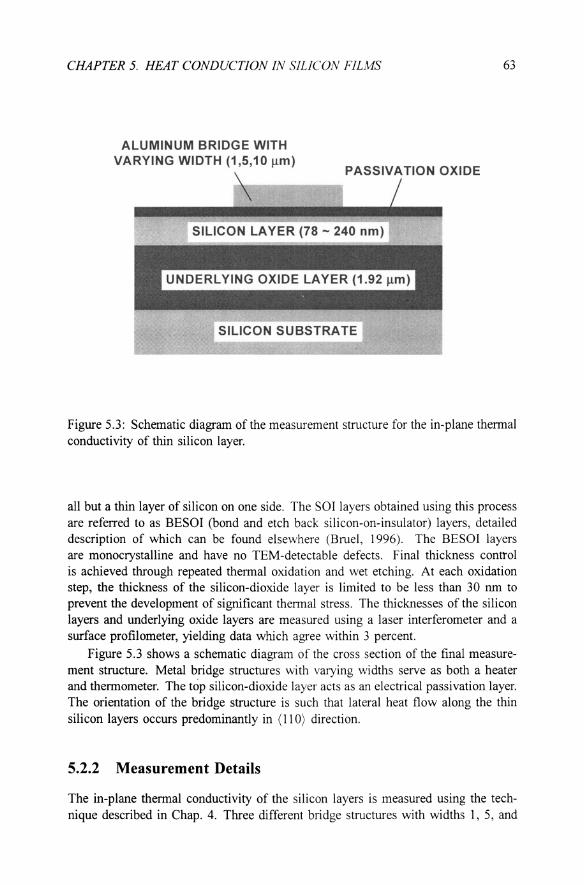
CHAPTER 5. HEAT CONDUCTION IN SILICON FILMS
ALUMINUM BRIDGE WITH VARYING WIDTH (1 ,5,10 11m)
PASSIVATION OXIDE
SILICON SUBSTRATE
63
Figure 5.3: Schematic diagram of the measurement structure for the in-plane thermal conductivity of thin silicon layer.
all but a thin layer of silicon on one side. The SOl layers obtained using this process are referred to as BESOI (bond and etch back silicon-on-insulator) layers, detailed description of which can be found elsewhere (Bruel, 1996). The BESOI layers are monocrystalline and have no TEM-detectable defects. Final thickness conttol is achieved through repeated thermal oxidation and wet etching. At each oxidation step, the thickness of the silicon-dioxide layer is limited to be less than 30 nm to prevent the development of significant thermal stress. The thicknesses of the silicon layers and underlying oxide layers are measured using a laser interferometer and a surface profilometer, yielding data which agree within 3 percent.
Figure 5.3 shows a schematic diagram of the cross section of the final measurement structure. Metal bridge structures with varying widths serve as both a heater and thermometer. The top silicon-dioxide layer acts as an electrical passivation layer. The orientation of the bridge structure is such that lateral heat flow along the thin silicon layers occurs predominantly in (110) direction.
5.2.2 Measurement Details
The in-plane thermal conductivity of the silicon layers is measured using the technique described in Chap. 4. Three different bridge structures with widths 1, 5, and

64 MICROSCALE HEAT CONDUCTION IN ICs
10 J-lm are employed in the present study. The width of the metal bridge and the extent of lateral heat spreading are chosen to be much larger than the silicon layer thickness, and hence the mean free path of phonons. This is to ensure that the in-plane temperature gradient and thermal conductivity retain their meaning. The measured frequency-dependent amplitudes of temperature oscillations are compared with numerical solutions to the heat diffusion equation to extract the thermal conductivity of the silicon and underlying silicon-dioxide layers. The thermal conductivity of the top silicon-dioxide layer (fig. 5.3) is measured separately using a silicondioxide layer with comparable thickness. The thermal conductivity of the metal layer is determined independently as explained below.
The accuracy of the present experimental technique to measure the in-plane conductivity of ultra-thin films is first verified. This is achieved by measuring the thermal conductivities of aluminum films with thickness comparable to those of the silicon layers. The aluminum films are sputtered on regular silicon wafers capped with 2 J-lm-thick LPCYD silicon-dioxide films. Electrons, which are the dominant heat carriers in pure metals, scatter with grain boundaries and film surfaces, resulting in the reduction in both electrical and thermal conductivity. The electronic thermal conductivity is related to the electrical conductivity via the Wiedemann-franz-Lorenz law, which was shown to be applicable for thin aluminum films of comparable similar thicknesses (Boiko et ai., 1973; Paul et ai., 1995). This is expected because electron - boundary scattering is elastic in nature and does not invalidate the analogy between charge and thermal energy transport by electrons. The thermal conductivity of the aluminum films studied is larger than 100 W m -l K -l and the lattice contribution is expected to be negligible. figure 5.4 plots the measured Lorenz numbers as a function of metal film thickness. The results of the present study agree very well with those of previous studies and add confidence in the subsequent measurements on the silicon layers. The main contributors to the experimental uncertainty in the present measurements are the uncertainty in the sample dimensions and the uncertainty in the calibration coefficient of the bridge thermometer.
figure 5.5 shows the measured in-plane thermal conductivities of the silicon layers at room temperature. The thermal conductivity is smaller by up to 50 percent than the bulk value and decreases slightly with decreasing film thickness. A previous study (Zheng et ai., 1996) using a free-standing silicon membrane structures reported roughly two orders of magnitude reduction, which is presumably due to dislocations or other defects introduced during the fabrication process (Chen and Neagu, 1997). Other existing data (Yu et ai., 1996; Asheghi et ai., 1996) on much thicker silicon films have large experimental uncertainties but are consistent with the present data.
5.3 Heat Conduction in Semiconductors at High Temperatures
This section develops a model for the thermal conductivity of covalently bonded semiconductors at temperatures higher than the characteristic temperature of the

CHAPTER 5. HEAT CONDUCTION IN SILICON FILMS 65
-N 3 ~
OJ ~ • • b .I. ....
7 ..... 2 • •• >< • -0::: BULK VALUE w m ::E 1 :::J Z AI • BOIKO et al. (1973) N • PAUL et al. (1995) Z W T = 300 K • PRESENT STUDY 0::: 0 0 ..J 60 80 100 300 500
FILM THICKNESS (nm)
Figure 5.4: The Lorenz number of aluminum films as a function of thickness.
zone-boundary TA phonons. A model parameter representing the frequency dependence of phonon-phonon scattering rate is extracted from the data on samples with known amount of point defects. The model constructed in this section is used to predict the thermal conductivity of crystalline silicon films in the following section.
5.3.1 A Thermal Conductivity Model
The present study adopts a semi-empirical approach to model phonon thermal conductivity in semiconductors on the basis of the Boltzmann transport equation. The Boltzmann equation can be applied rigorously in the analysis of heat transport when the weak scattering condition ..JT > > 1 is satisfied (Cahill, 1997), which is true for most crystalline solids. Phonons are classified into the propagation mode and the reservoir mode (Armstrong, 1981), with the fonner mode considered as carrying all the heat. This is a reasonable approximation for the semiconductors under consideration because of the presence of highly dispersive transverse acoustic phonon and optical phonon branches. Phonons with nearly zero group velocity or small lifetimes remain in equilibrium and act as a heat reservoir for the propagation mode. The departure of the phonon occupation number, nil, from the thennal equilibrium value, nij',eq, can be expressed as (Ziman, 1960)
nif- n'l,eq = <I>(q)[8nq/8(nwif)]' (5.2)

66
~
~ ":"e
~ >l-S; ~ o ::l C Z o o ...J « :E 0:: w :I: I-
MICROSCALE HEAT CONDUCTION IN ICs
150 ~--------------------------~--, T = 300 K •• _ •• ----.---------------- -----
.' .'
100
50 (L)
.' ......... . '
_-.(GRAY)
Asheghi et aI., (1998) Zheng et al. (1996)
OL....---........ -------------:::......-:....-....:... ....... 100 1000
501 LAYER THICKNESS (nm)
Figure 5.5: The in-plane thermal conductivities of thin silicon layers at room temperature.
where (5.3)
Here if is the phonon wavevector, vij is the group velocity, and 7 is the relaxation time. Note that the departure from equilibrium is small for phonons with small group velocity or small relaxation time.
In the present study, the propagation mode is represented by the characteristics of the longitudinal phonon branch based on the considerations presented in Sec. 5.1. This is an approximation, but the resulting error is not expected to severely limit the applicability of the model provided that the longitudinal phonons account for the majority of heat currents.
To derive an expression for the thermal conductivity, one needs to model various scattering processes. The present work models the phonon - phonon scattering using a single-mode relaxation time, which will be discussed shortly. The total relaxation time is obtained by combining the relaxation time for phonon - phonon scattering, 7 pp , with that for phonon - point defect scattering, 7/, using the Matthiessen's rule. An expression for the thermal conductivity can then be given in terms of the relaxation times:
4 J 'TL 2 -2 kBT j Vgr·r cxp(x)(exp(x) - 1) d k= --3 - x.
61r2 1i. 0 Vph 1/7pp (x) + 1/7/(x) (5.4)

CHAPTER 5 HEAT CONDUCTION IN SILICON FILMS 67
The single-mode relaxation time can be understood with reference to a linearized phonon Boltzmann transport equation (Klemens, 1958)
dn( if! n(ifJ '" _ --- = --(;;'\ + ~ W(q.r1ln(q'). dt a q) _
(5.5)
'/#(1
Here n is the departure from equilibrium of the phonon occupation number, a is the single-mode relaxation time, and if is the phonon wave vector. The second term in the right hand side of Eq. (5.5) represents the change in the relaxation rate of a phonon due to the departure from equilibrium of all the other phonons. If n's of all modes interacting with a single mode if vanish, the particular single mode would return to equilibriuin with a relaxation time of a (if!.
The resistive phonon - phonon scattering is assumed to be dominated by scattering processes that link the propagation mode to the reservoir mode. The three-phonon normal process involving only the longitudinal phonons has very low probability due to the requirements imposed by energy conservation and wavevector selection rules. Now that the reservoir mode is practically in equilibrium, the phonon - phonon scattering can be modeled using a single mode relaxation time. This approximation is further supported by a recent study on the phonon normal process in anisotropic crystals (McCurdy, 1994). The study showed that, unless rather restrictive conditions are met, the phonon normal process cannot preserve a drifted phonon distribution and consequently acts as a resistive process.
The frequency dependence of tpp is modeled using a functional form
1 () m -=BTx. 7p1'
(5.6)
While the actual dependence can be fairly complex because of the crystal anisotropy and phonon dispersion, detailed theoretical or experimental study is still absent. In anticipation that the thermal conductivity, which is a sum of the contributions from all phonons, is not sensitive to fine details of this dependence, the present study employs the aforementioned functional form treating In. and B as adjustable parameters. The resulting relaxation time should be regarded not as a well-determined value but instead be treated as an effective one. Further discussion is provided in Sec. 5.3.2, where a value of 'm'used in the present study for silicon is determined.
Phonon - point defect scattering is modeled in the following fashion. When the separation between individual point defects is large enough, the defects can be treated as isolated scattering centers. The total scattering rate can be represented as the sum of the individual contributions. The rate of phonon scattering due to a certain type of point defect with number density c can be written as (Tamura, 1983)
1 1T .) -( -) = -c[hl..J- D(w). 7[ ..J 6
(5.7)
where V() is the volume per atom, D is the phonon density of states per unit volume, and r characterizes the scattering strength. Equation (5.7) states in essence that

68 MICROSCALE HEAT CONDUCTION IN ICs
the phonon-point defect scattering rate is proportional to the number of available phonon states into which phonons can scatter. When the Debye model is employed, the phonon density of states is proportional to the square of the phonon frequency and the familiar w4-dependence is recovered. A high degree of dispersion, such as that exhibited by the transverse acoustic phonon branches shown in Fig. 5.1, results in a high phonon density of states and hence high phonon-point defect scattering rates. An expression for r was derived for cubic crystals: (Klemens, 1955; Abeles, 1963)
( 6.M) 2 [6.1 6.R] 2 r = M + 2 T - 2 x 3.2'R (5.8)
where M, 1, and R are the average values of the atomic mass, force constant, and ionic radius in the crystal respectively, and 6.M, 6.1, and 6.R represent their respective perturbations due to point defects. The quantity, denotes an average GrUneisen parameter, which characterizes anharmonicity of the bonds. The contributions due to differences in ionic radii and perturbations in interatomic potentials are generally negligible for isotopes. These factors can be important for certain other types of point defects but their magnitudes are usually hard to estimate.
By using the Debye model, the relaxation rate of phonon - point defect scatterings can be expressed for the high-frequency longitudinal acoustic phonons as
1 Vr)r....,4 TJ(W) = 127r V~hVgr'
(5.9)
where v is the magnitude of phonon propagation velocity. The phonon spectrum is assumed to be isotropic. Equation (5.9) reflects the fact that the requirement of energy conservation permits high-frequency longitudinal phonons to scatter only into longitudinal phonons. This expression underestimates the phonon - point defect scattering rate for low-frequency LA phonons, which can scatter into both the TA and LA phonon branches. This is not expected to introduce large errors since phonon - point defect scattering is not a dominant mechanism for the low-frequency LA phonons.
5.3.2 Thermal Conductivities of Germanium Samples with Point Defects
The model developed in Sec. 5.3.1 is first applied to germanium samples with silicon impurities (Bakhchieva et aI., 1984) and to isotopically enriched germanium samples (Geballe and Hull, 1958; Asen-Palmer et aI., 1997). Germanium is chosen as a model semiconductor because of the existence of considerable amount of experimental work. This is due, in part, to the ease with which high-quality crystals with controlled amount of point defects can be produced. In view of the close similarity between the phonon spectra of silicon and germanium, it is deemed reasonable to assume that the parameter '(II" which describes the frequency dependence of phonon - phonon scattering rates, is very close for the two materials.

CHAPTER 5. HEAT CONDUCTION IN SILICON FILM')
"TE
~ >..... :> i= o ::> c z o o ..J « :2: 0::: W J: .....
150
100
50
.. - ..... Q ..
i I I
I
•••••••••••••• .0
0 Genal
I Ge : Si (0.77%) f'.. Ge : Si (5.25%)
••••••• .0._ ••• _ ~-.-. '-'-'
•.•.•.•.•. ~-.•... -.~-.-.-.-.-.-.-.-.-.-.-c,._._._
o ~------------------------------~ 150 200 250 300
TEMPERATURE (K)
69
Figure 5.6: Comparison of the predicted and measured thermal conductivities of germanium with various concentrations of isotopes and silicon impurities.
The mass difference between germanium and silicon has been estimated to account for over 90 percent of the scattering cross section of a silicon atom in germanium lattice (Toxen, 1961). As a consequence, the phonon - point defect scattering rate can be evaluated with greater confidence than other impurities, where the differences in ionic radii and perturbations in interatomic potential can add hard-toestimate components. Germanium samples doped with silicon alloys are treated on the same footing as an isotopic mixture with mass fluctuation scatterings.
Figure 5.6 shows the temperature dependent thermal conductivity of bulk germanium samples with different concentrations of silicon impurities. For each trial value of 'In, the function B is first fitted to the experimental data for the isotopically enriched germanium sample (Geballe and Hull, 1958). The thermal conductivities of the samples with point defects are then computed and compared with the data. The best fit is obtained for the exponentm near 1.5, which lies between the value of one proposed by Landau and Rumer from the consideration of sound wave attenuation and the value of two inferred from the energy and wavevector conservation rule (see, for example, Herring, 1954; Holland, 1963). The present value should be regarded as an effective value approximating more complicated frequency dependence and reflecting the influence of those phonons not formally included in the analysis.
The present model reproduces the thermal conductivity of samples with point defects reasonably well over the entire impurity concentration and temperature ranges

70 MICROSCALE HEAT CONDUCTION IN ICs
considered. Since the nonresistive nonnal process is expected to influence the conductivity in a manner sensitive to the temperature and strength of phonon-point defect scattering, this agreement indirectly supports the use of a single-mode relaxation time in the present model. When scaled with respect to the Debye temperature, the temperature range considered for gennanium is roughly equivalent to room temperature and above for silicon.
5.4 Prediction of the In-Plane Thermal Conductivity of Silicon Thin Films
This section is devoted to the prediction of the in-plane thennal conductivity of thin silicon films using a solution to the Boltzmann transport equation accounting for phonon-boundary scattering. The phonon relaxation time obtained for bulk samples in the preceding section is used for this prediction. Possible phonon scattering arising from defects unique to thin films are neglected. This is a good approximation for silicon-on-insulator (SOl) layers of interest here and also for semiconductor layers, such as gallium arsenide and aluminum arsenide layers, in superiattices, which are high-quality single-crystal materials.
Charge and energy transport by electrons, radiative energy transport by photons, as well as vibrational energy transport by phonons are often described using the Boltzmann transport equation. Assuming that no additional complications arise due to the phonon nonnal process, many of the solutions accounting for the size effect for electronic conduction (e.g., Sondheimer, 1952 ; Ziman, 1960) and for radiative heat transfer (e.g, Chen and Tien, 1993) can be applied to phonons.
The nature of phonon-boundary scattering, which can be approximately described by the specularity parameter, was shown to influence the size effect (Ziman, 1960; Klitsner and Pohl, 1987; Chen, 1997b). Klitsner and PoW (1987) experimentally investigated the nature of phonon-boundary scattering at the surface of silicon samples, on which various types of films were deposited. When the transmission of phonons across the interface is significant, the phonon-boundary scattering was found to be governed mainly by the scattering of phonons inside the films. For silicon-oninsulator (SOl) structures studied here, diffuse scattering of phonons at the interface between silicon and amorphous silicon dioxide layers is assumed. This is reasonable in view of the close matching of acoustic properties of silicon and silicon dioxide and also the fact that the mean free path of phonons in amorphous silicon dioxide is orders of magnitude smaller than that in silicon. The assumption is further supported by the recent theoretical study of the size effect. The solution of a radiative transport equation in periodic two-layer systems with nonvanishing specularity factor (Chen, 1997b) reduces to that for the diffuse boundary scattering in the limit where the phonon transmission coefficient is unity and the phonon mean free path in one layer is negligible compared with that in the neighboring layer.
When the scattering at the surface or interface is diffuse, the ratio of the thin-film phonon relaxation time, Tfi/m, or mean free path, Afi/m , to their bulk counterparts

CHAPTER 5. HEAT CONDUCTION IN SILICON FILMS 71
can be evaluated from (Sondheimer, 1952):
3 1 3. 3 -b 5 15 15 2 _ b S = 1- 4(15 - 12 15 )El(-I5) - 815(1- e ) - (-8 + 16 - 16)e . (5.10)
Here, 15 is the ratio between the mean free path and film thickness. By incorporating T film into Eq. (5.4) for the longitudinal phonons or by using A film for the transverse acoustic phonons, the in-plane thermal conductivity of thin films can be predicted.
Figure 5.5 also plots the predicted in-plane thermal conductivity of pure silicon layers at room temperature as a function of film thickness. The upper most curve labeled as gray uses the mean free path estimated without taking into account phonon dispersion and frequency dependence of phonon scattering. The gray medium approximation uses the kinetic theory expression Agmy = 3k/Cv, where C taken to be the bulk heat capacity and v the speed of sound, and considerably underestimates the size effect. The other two curves assume either longitudinal or transverse phonons as the sole heat carriers. The experimental data show reasonable agreement with the prediction when the longitudinal phonons are considered to be the dominant heat carriers. This supports the view that high-frequency phonons with short mean free paths contribute appreciably to heat conduction. This finding is consistent with a previous study of the thermal conductivity of germanium (Sood and Roy, 1993), which concluded the dominance of longitudinal phonons based on the results from their extended Callaway'S model.
The third prediction assumes that the TA phonons are the sole heat carriers. An estimation for the mean free path of the transverse acoustic phonons, AT, is made by means of the gray medium approximation discussed in Sec. 5.1. The gray medium approximation is expected to be reasonable for the TA phonons since phonon states with appreciable group velocity are concentrated within the narrow frequency interval. Compared with the phonon group velocity, the phase velocity is much less sensitive to details of the phonon dispersion curve. This offers an advantage in characterizing the transverse acoustic phonons, because their spectra exhibit rather pronounced anisotropy compared with that of the longitudinal phonons. Approaches based on the relaxation time require the phonon group velocity explicitly and thus become difficult to implement. Although phonon dispersion in a particular crystal direction can be readily represented with high accuracy using the existing lattice dynamics models, incorporation of the anisotropy in phonon spectra and its impact on phonon relaxation rates await further investigation. The small group velocities of the TA phonons lead to the mean free path over one micrometer and, hence, a very pronounced size effect. For this large value of the mean free path, significant specular phonon reflection at the interfaces would be necessary to explain the present data.
Savvides and Goldsmid (1973) measured the thermal conductivity offree-standing silicon films of various thicknesses. For the pure samples no size effect was observed for the films as thin as 20 micrometer, while those samples with neutron irradiationinduced point defects displayed systematic reduction in their thermal conductivity. This phenomenon was attributed to the strong frequency-dependence of phononpoint defect scatterings, which causes enhancement in the relative contribution to

72 MICROSCALE HEAT CONDUCTION IN ICs
heat conduction from the low-frequency phonons. Modeling of the thermal conductivity of samples with a significant amount of point defects is itself a nontrivial task due partly to the complications arising from interactions among phonon scattering mechanisms. Although quantitative analysis of the size effect on these samples is difficult for this reason, it can be concluded that the data cannot be readily reconciled with models which assume that the high-frequency transverse phonons within a very narrow frequency range account for the majority of the heat current.
A recent theoretical study (Balandin and Wang, 1998) considered the effects of film boundaries on the phonon dispersion and predicted much stronger thickness dependence. The phonon confinement effect is expected to be important when the wavelength of dominant phonons is comparable to the thickness of a film, and is therefore not relevant here.
As one convenient measure, the effective mean free path can be defined as the thickness of a film for which k fi1m / klmlk is equal to the value given by Eq.(5.l 0) for unity b. When the longitudinal phonons are assumed to be the dominant heat carriers and Tn = 1 is used, the effective mean free path is found to be around 0.3 /lm. This value is roughly one order of magnitude larger than Agray. Still larger values are predicted when stronger frequency dependence is used for the phonon-phonon scattering or when the transverse phonons are taken to account for the entire heat conduction.
5.5 Simplified Phonon Transport Equations Accounting for Phonon Dispersion
Previous studies of microscale lattice heat conduction solved the phonon Boltzmann transport equation (Levinson, 1980; Klitsner et aI., 1988, Mahan and Claro, 1988; Majumdar, 1993; Chen, 1997a) but no distinction was made between the propagation and reservoir modes. The distinction is not critical at low temperatures where heatcarrying phonons are practically identical to energy-containing phonons. At elevated temperatures, in contrast, highly dispersive phonon branches are fully excited and account for a major portion of the heat capacity. Considerations of phonon dispersion are essential in this case. In simulating operation of a field-effect transistor made of gallium arsenide, Fushinobu et al. (1995) divided the phonon system into the acoustic and optical phonon branches. This was mainly to account for the fact that high-energy electrons interact preferentially with the optical phonons. These authors, however, treated energy transport by the acoustic phonons using the heat diffusion equation and did not consider non-local effects.
It is in principle possible to obtain a complete solution of the phonon transport equation accounting for phonon dispersion but the expense involved is often difficult to justify in practical engineering calculations. This is particularly the case given considerable uncertainties in microscopic parameters involved. An alternative approach is proposed here, which solves a pair of transport equations corresponding to the propagation mode and the reservoir mode, respectively.

CHAPTER 5. HEAT CONDUCTION IN SILICON FILMS 73
To avoid algebraic complexity, we restrict the discussion to a one-dimensional situation. A phonon Boltzmann transport equation can be written under the relaxation time approximation as
anq + f.-tvq anq = nij",eq - nij" at a.T Tij
(5.11)
where f.-t is the directional cosine defined with respect to the x-axis. The quantity nij"
is the phonon occupation number and is in general direction-dependent. Equation (5.11) is separated into two equations, corresponding to the propagation mode and to the reservoir mode. We define elf as the relative energy of phonons per unit volume and per unit solid angle
elf = ./nw[nq - nq,eq(Tref)]D(..v)dw. (5.12)
The equilibrium phonon occupation number at some reference temperature Tref is denoted by nq,eq(Tref)' To take advantage of symmetry, Eq. (5.12) is integrated over the entire circumferential angle, (j), of which nij' is assumed to be independent. The integration yields
I /.211" lid e = C (]J •
. 0 (5.13)
To further simplify the analysis, we assume that the phonon heat capacity is independent of temperature. This is a good approximation when temperatures under consideration are high relative to the Debye temperature or when temperature variations in the system are small. The directional phonon energy density can be expressed in a very compact form
(5.14)
Since the propagating mode can deviate considerably from equilibrium, its temperature is not well-defined in a conventional sense. The temperature of the propagation mode T p and the lattice temperature T L are defined here as a measure of the average phonon energy density:
Tp - Tref = (lll e'pdf.-t) lep . (5.15)
(5.16)
Here the subscript P labels the propagation mode, R the reservoir mode, and L the lattice system as a whole. Under general nonequilibrium conditions, the lattice temperature as defmed here are closer to TR than to Tp because the heat capacity of the reservoir mode is typically many times larger than that of the propagation mode.
Integrating the Boltzmann equation over the frequency intervals appropriate for the propagation mode, one gets
ae'p ae'p _ { !Cp(h - Teed - r'p } a + IlVp a - . t x Tp
(5.17)

74 MIC ROSCALE HEAT CONDUCTION IN ICs
The mean propagation speed and relaxation time for the propagation mode are denoted by Vp and Tp, respectively. A similar equation can be derived for the reservoir mode. Since the reservoir mode has an isotropic equilibrium distribution, additional integration can be performed over the entire azimuthal angle to yield
Cn a(Tn - Trror) = _ {Cp[(h - Tref l - (Tp - Tref l] } . at Tp
(5.18)
The right-hand side of Eq. (5.18) follows from the requirement on the overall energy balance and Eq. (5.15). Equations (5.17) and (5.18) form a system of equations that needs to be solved simultaneously to analyze transient microscale heat conduction.
The physical meaning of Eqs. (5.16) and (5.18) can be understood as follows. Since the group velocity of the reservoir mode is zero, the transport of thermal energy is due entirely to the propagation mode. As the propagating mode travels down the temperature gradient, its excess thermal energy is transferred to the reservoir mode via phonon scattering processes represented by the right-hand side of the equations. The net energy transfer between the modes vanishes under equilibrium conditions where the mode temperatures are equalized.
As an illustrative example, we consider the time-evolution of temperature fields in a semi-infinite pure silicon sample, which is initially at a uniform temperature To and experiences a step change in the surface temperature. The longitudinal acoustic phonons are considered to be the propagation mode based on the observations made in Chap. 5. The mean relaxation time of the propagation mode is taken to be a weightedaverage value of the frequency-dependent phonon relaxation time, Tp = 3k/Cpv~. The heat capacity of the longitudinal phonon is evaluated from
k~ 3 /(hI T 1 x4ex
Cp=~T ~(e_l)2d.T, 27r n. . 0 ph gr
(5.19)
where Vph and Vqr are the phase and group velocities, respectively, and 83 is the characteristic temperature of the longitudinal phonons at the zone boundary. The group velocity of the high-frequency longitudinal phonons is used as the propagation velocity, Vp. Numerical values of the parameters are those of Holland (1963), who approximated the longitudinal phonon spectrum using two linear segments. The mean relaxation time, Tp, thus evaluated is around 70 ps at room temperature. To properly account for the temperature variation within the sample, Tp needs to be considered as position and time dependent. These dependencies, however, can be neglected for small temperature rises, which is assumed to be the case here.
The boundary conditions are
Tn(x = 0, t) - Tnf = Ts - Tref , (5.20)
(5.21 )
for the reservoir mode and
e'p(x = 0, f.L > 0, t) = Cp(Ts - Tref )/2, (5.22)

CHAPTER 5. HEAT CONDUCTION IN SILICON FILMS 75
-------- PROPAGATION
0.8 -- RESERVOIR -0 t-
I/) 0.6 !:::. -- 0.4 0 t-
t-0.2 -
................ -0
0 2 3 4 5
xl A
Figure S.7: Spatial temperature distributions of the propagation and reservoir modes in a silicon sample, which experiences a step-change in surface temperature at time t = O. The parameter Tp is the mean relaxation time estimated for the longitudinal phonons, which are assumed to be the dominant propagation mode. The numerical value of Tp used in the present calculation is 70 ps.
e'p(oo, J.L < 0, t) = Cp(To - Tre! )/2 (5.23)
for the propagation mode. In discretizing the transport equations (5.17) and (5.18), the explicit Euler method is used for the time variable and the one-sided upwind scheme is used for the spatial variable. The Gauss-quadrature method is employed to evaluate the integral with respect to the directional cosine in Eq. (5.17). The solution procedure adopted is similar to \vhat was used by Joshi and Majumdar (1993). As one test of the accuracy of the present solution approach, the steady-state temperature distribution across two parallel plates maintained at fixed temperatures is obtained and compared with the exact analy1ic solution (Siegel and Howell, 1992). The numerical solution does not deviate from the analytic solution by more than 5 percent. In all of the simulation reported here. the grid spacing and the size of time steps are reduced until the refined solution does not ditTer by more than 5 percent from the coarser grid solution.
Figure 5.7 shows the spatial temperature distributions for the propagation and reservoir modes at four different times after a step-change in surface temperature

76
- 0.8 Q .-VI .- 0.6 ---Q .- 0.4 ...J
t:. 0.2
0
0 2
MICROSCALE HEAT CONDUCTION IN ICs
4
DIFFUSION EQUATION
TWO-FLUID MODEL
6 8
xl A
10
Figure 5.8: Time-evolution of lattice temperature profiles and their comparison with solutions to the heat diffusion equation.
is imposed. A significant difference between the mode temperatures exists at times comparable to Tp. At t = Tp the spatial extent of the region that has responded to the change in the surface temperature is close to the mean free path for the propagation mode but is smaller for the reservoir mode. The temperatures of the two modes approach each other as more time elapses, allowing them to interact with each other more strongly.
Immediately after the surface temperature is raised, the temperature of the propagation mode is equal to the average value of the surface temperature, Ts, and the initial temperature of the sample, To. This can be understood by recalling that Tp is defined as a measure of the average phonon energy density. Phonons impinging on the surface have temperature To while those emanating from the surface are characterized by the temperature Ts. The temperature slip at the surface, however, becomes negligible as the heat affected region extends farther into the sample interior. Local description becomes adequate for heat transport when the characteristic lengthscale, here the heat diffusion length, becomes much greater than the mean free path.
Figures 5.8 and 5.9 compare the solutions to the heat diffusion equation with those obtained from the transport equations developed here. The heat diffusion equation is unable to predict the temperature slip at the surface and yields surface heat flux that diverges as time t approaches zero. The diffusion equation becomes

CHAPTER 5. HEAT CONDUCTION IN SILICON FILMS 77
- 5108
'liE •• - DIFFUSION
~ ••••• DIFFUSION + RESISTANCE
- - TWO·FLUID MODEL
>< :::J ...J I.L .... 2.5108 R =2A/3k « 5
W ::a::: W 0 c( I.L 0:: :::J
010° en 0 20 40 60 80 100
t I tp
Figure 5.9: Comparison between the surface heat flux calculated using the transport equations derived in the present work and that obtained from the heat diffusion equation with and without an artificial thermal boundary resistance.
a better approximation at larger values of t. The finite propagation speed of heat waves can be captured by the hyperbolic heat equation. The heat wave formulation does not incorporate nonlocal nature of heat transport and yields results similar to those of the diffusion equation at times larger than the phonon relaxation time (Joshi and Majumdar, 1993).
Figure 5.9 also plots the prediction, which is again based on the heat diffusion equation but includes artificial thermal boundary resistance at the surface. This modification leads to better agreement at small time t and eliminates the divergence at t = O. Significant improvement is also achieved in predicting the spatial temperature distributions as illustrated in Fig. 5.10. The proposed modification is motivated by the diffusion approximation to steady-state radiative transport, which exhibits excellent agreement with the exact solution (e.g., Siegel and Howell, 1992). The artificial boundary resistance used here is also a good approximation in predicting the temperature slip for a spherical geometry (Viskanta and Crosbie, 1967), which well approximates quantum dots and localized hot spots along drain junctions in FET's.

78 MICROSCALE HEAT CONDUCTION IN ICs
-- DIFFUSION + RESISTANCE
- 0.8 ..••.•.. TWO-FLUID MODEL
0 .... Ul
R = 2A 13k .... 0.6 - 5 --0 .... 0.4 -I
t:.. 0.2
0
0 2 4 6 8 10
xl A
Figure 5.1 0: Temperature profiles calculated using the heat diffusion equation and incorporating thermal boundary resistance of 2 A / 3 k at the surface.
5.6 Hot Phonon Effects
The temperature slip observed in the above calculations deserves further discussion, which has implications for both thermal and electrical characteristics of microdevices. The understanding of the temperature slip also clarifies the nonequilibrium nature of the heat transport process.
Consider a medium bounded by two infinite parallel walls which are maintained at two different temperatures. When the mean free path of heat carriers in the medium is comparable to or larger than the wall separation dw , the temperature of the medium in the vicinity of the wall differs from the wall temperature. One extreme case is where the mean free path is considerably larger than dw such that the carriers originating from the two walls do not interact with each other during their flight across the medium. At each point in the medium two types of carriers coexist and the medium would be at the average of the wall temperatures. Even when the internal scattering is not entirely negligible, temperature slips at the walls are developed much like the one observed in the transient case.
To have a nonvanishing net heat flux, the angular distribution of phonon intensity must be asymmetric with respect to the direction perpendicular to the temperature gradient. The distribution can be characterized by two average temperatures Tfp
CHAPTER 5. HEAT CONDUCTION IN SILICON FILMS 79
and np , each corresponding to carriers traveling in the forward and backward directions, respectively. The two temperatures are related to the net heat flux q and medium temperature TL: q = Cv(Tfp - np )/4 and TL = (Tfp + np )/2 in the one-dimensional case. The temperature of the forward propagating carriers exceeds TL by !:::.Tf = 2q/Cv.
The preceding discussion is general and not restricted to phonon heat transport in semiconductors or dielectric materials for which the distinction between the reservoir and propagation modes is necessary. A key difference phonon dispersion makes is that heat currents are distributed unevenly among different phonon modes, so that the degree to which some phonons depart from equilibrium is correspondingly higher. The excess temperature !:::.Tf, for instance, is inversely proportional to the heat capacity of dominant heat carriers, which can be substantially smaller than the bulk value.
Nonequilibrium phonons are produced not only by temperature gradients but also by high electric fields, such as those present at the drain junction of fieldeffect-transistors. Electron - phonon scattering processes require that special selection rules be satisfied favoring phonons with certain polarizations and wavevectors over others. The preferential interaction of high-energy electrons with longitudinal optical phonons in polar semiconductors has been a subject of several studies (e.g., Kocevar, 1985). The nonequilibrium situation affects the electron-phonon scattering rates and influences the interparticle correlation via reabsorption of previously emitted phonons. These effects have been shown to exert significant influence on electronic noise in semiconductor devices (Bordone et aI., 1993). The importance of the propagation mode derives from the fact that the major decay channel of the optical phonons involves the propagation mode. The temperature of the propagation mode with which the longitudinal optical phonons interact can be higher than the lattice temperature calculated from the diffusion equation. Furthermore, nonlocal effects associated with relatively long mean free paths of the propagation mode contribute to the modification of the electron-electron correlation functions.

Chapter 6
Summary and Recommendations
The present research develops high temporal and spatial resolution thermometry techniques and applies them for the thermal characterization of integrated circuit elements and thin films. An experimental setup is constructed that integrates high resolution scanning optical thermometry capability into an electrical probing facility. Spatial resolution near 500 nm and temporal resolution better than 100 ns have been demonstrated using high voltage transistors and interconnects subjected to brief electrical stresses. The two step temperature calibration method developed here is well suited for microdevices and can be easily extended to other types of optical thermometry techniques. The thermometry technique also plays a key role in the extraction of the thermal transport properties of thin films. Simultaneous measurements of thermal conductivity anisotropy and volumetric heat capacity can be performed. Data on CVD silicon dioxide indicate that degree of disorder in atomic arrangements affect the thermal conductivity of amorphous solids. The experimental capability and physical understanding will help characterize and design new dielectric passivation layers.
In order to investigate the mechanism of heat transport in silicon and provide data for the simulation of SOl devices, the present study also measures the thermal conductivities of crystalline silicon layers as thin as 80 nm. A large thermal conductivity reduction is observed for films with thickness commonly encountered in practical SOl devices. The data are analyzed using a model based on the phonon Boltzmann transport equation, which suggests that high frequency longitudinal phonons with relatively short mean free paths account for a large fraction of heat currents. A simplified set of transport equations is derived which account for phonon dispersion.
The following recommendations are made for future research on microscale heat transport in integrated circuit elements.

82 MICROSCALE HEAT CONDUCTION IN ICs
6.1 Atomistic Simulations of Heat Transport
While theoretical studies based on semi-phenomenological approaches provide insight into the physical mechanisms that underlie heat transport, atomistic simulations would ultimately be needed to achieve more detailed understanding. Recent studies employed molecular dynamics simulations to compute the lattice thermal conductivities of silicon carbide (Li et al., 1998) and the vibrational dynamics of amorphous solids (Mazzacurati et al., 1996). Future studies can perform simulations to investigate the effects of degree of disorder on the thermal conductivity of amorphous solids, which have been suggested in the present experimental data.
Molecular dynamics simulations require accurate interatomic potentials. Recent studies revealed that phonon spectra and Grilneisen parameters calculated using existing potential models for silicon deviate considerably from the experimental data (Porter et al., 1997). More refined interatomic potentials need to be derived before reliable simulations can be carried out.
6.2 Thermal Conductivities of Nanostructures
Various semiconductor nanostructures can be produced using nano-fabrication and epitaxial film growth technology. Thermal characterization of some of these nanostructures can be performed using variants of the techniques developed in the present study. One example is silicon nano-pillar structures embedded in a silicon-dioxide passivation layer. By comparing the conductivity of the silicon-dioxide layer with and without nano-pillars, the effective thermal conductivity of the pillars can be extracted.
In the limit where the dimension of a nano-structure is comparable to the coherence length of lattice vibrations, the wave nature of lattice vibrations cannot be neglected. Measurements in this regime will reveal interference between lattice waves and other phenomena that have not been observed in larger systems. Reduced dimensionality due to phonon confinement will decrease phonon heat capacity and also phonon scattering rates. Phonon - point defect scattering, for example, is proportional to phonon density of states.
6.3 Detailed Simulations of Semiconductor Device
Currently available device simulation tools solve the heat diffusion equation to obtain temperature information. The present study, however, shows that non-local nature of heat transport is already significant for deep sub-micron devices. Future studies on the impact of non-equilibrium phonon distribution on electron mobility and electron correlation functions are necessary. A set of simplified phonon transport equations derived in the present study can serve as a basis on which more refined simulation tools for semiconductor devices can be built.

Appendices

Appendix A
Uncertainty Analysis
This Appendix contains uncertainty analyses for the experimental data reported in the preceding chapters. The total uncertainty is calculated based on the root sum of the squares of the uncertainties in all the contributing measured quantities.
A.I Uncertainty in the Temperature Rise
Experimental uncertainty in the temperature rise measured using the thermoreflectance technique stems from uncertainties in the calibration coefficient, CT R, and photodetector output voltage measurements. The relative importance of the two contributions depends on the calibration method employed and the measurement timescale. Noise in the detector output is the major source of uncertainty in short-timescale thermometry experiments.
When the two-step calibration method is used, the uncertainty in CT R stems primarily from uncertainty in the temperature coefficient of resistance (TCR) of a microfabricated metal line that is used as a reference thermometer. The uncertainty in TCR is estimated by considering uncertainty in the measured electrical resistance and uncertainty in the temperature reading from a thermocouple attached to the substrate. By taking into account both statistical fluctuations and instrument resolution, we estimate the relative uncertainty in the electrical resistance to be 0.06 percent. The uncertainty in the temperature reading is near 0.5 K. The uncertainty in TCR is estimated by perturbing measured electrical resistance values and temperatures by their respective uncertainties, and then comparing the linear regression results of the resulting R vs T curves. The total uncertainty in TCR, taken to be one half the difference between the maximum and minimum values obtained in this fashion, is about 2 percent of the average value of TCR. Based on this, the relative uncertainty in CT R, which is relevant for the interconnect thermometry, is estimated to be 2 percent.

86
When the conventional calibration approach is employed instead, statistical uncertainty, which results partly from variations in the optical alignment during calibration, becomes a dominant component. In the particular case of the SOl transistor thermometry reported in Chap. 3, the total relative uncertainty in CTR is estimated to be 10 percent.
The uncertainty in the detector output voltage comes from statistical fluctuations and oscilloscope voltage resolution. For the SOl transistor thermometry, this results in around 4 percent relative uncertainty in the peak D.T. The corresponding value for the interconnect thermometry is larger, around 8 percent, due to much shorter timescales involved.
A.2 Uncertainty in the Thermal Properties of Dielectric Films
Uncertainty in the out-of-plane thermal conductivity of a dielectric film arises from uncertainties in the measurement structure dimensions (w, L), film thickness (d f ), heat generation rate (P), and temperature rise (D.T). In symbolic form,
8k = j[8k]~ + [8k]i + [8k]~, + [8k]~ + [8k]~T' (A. 1)
The width of the metal bridge structures is determined from scanning electron micrograph and also from its electrical resistance. The thickness of the dielectric films is determined using a surface profilometer, a laser interferometer, and a scanning electron microscope. The uncertainties in the dimensions are estimated by comparing results from independent measurements. In the present uncertainty analysis, maximum deviations from the average value are taken as uncertainties. Typical values of estimated uncertainties are: 8w I w = 2 percent, 8d tI d f = 3 percent, and 8 L I L = 0.2 percent. The uncertainty in the temperature rise is dominated by the uncertainty in TCR, which is discussed in the preceding section. For an LPCVD silicon-dioxide film with thickness 1 J.Lm, the contribution from each component is: [8k]w = 0.02, [8k]L = 0.002, [8k]d, = 0.03, [8k]p = 0.0034, and [8kbT = 0.02. The total relative uncertainty is 4.2 percent.
Similar analysis can be performed for the uncertainty in the heat capacity of thin films. The solution of the two-dimensional conduction equation is fitted to the experimental data while systematically perturbing quantities involved. These quantities include the dimensions of metal bridge structures, thickness of dielectric films, current, electrical resistance, TCR, voltage reading from a lock-in amplifier. For a 2 J.Lm-thick LPCVD silicon-dioxide film, typical relative uncertainty values are: [8Cf]vIC, = 0.061, [8Cf]TCRICf = 0.045, [8Cf]wICf = 0.044, [8C,ld",IC, =
0.038, [8Cfld,IC.r = 0.029, [8C.rlcmICf = 0.025, [8C.rldCf = 0.011, [8Cf lR/Cf = 0.014, and [8Cf]LICf = 0.0045. The total relative uncertainty is estimated to be 10 percent.

87
A.3 Uncertainty in the In-Plane Thermal Conductivity of Thin Films
Uncertainties in the thermal conductivity ko and thickness do of a buried silicondioxide layer, and uncertainties in the measured temperature rise of a metal bridge structure llT are dominant contributors to experimental uncertainty in the in-plane thermal conductivities of aluminum and silicon films. The overall uncertainty is estimated from
6k = [6kl~" + [6klt + [6kliT + [6kl~f + [6klko + [6kli + [6kl;, + [6kH, CA.2)
where Ro is the thermal resistance of the upper passivation layer that separates the metal bridge structure from the aluminum or silicon layer. Amplitude of AC current in the metal bridge is denoted by I. For the aluminum film of thickness 150 nm, each term of the above expression gives rise to relative uncertainty of 5.0, 6.6, 5.7, 2.9, 3.1, 0.58, 1.85, 0.98, 0.18 percent, respectively. The total uncertainty obtained from the root sum of the squares of the individual components is 11 percent. For the thinnest silicon film, a similar analysis yields illlcertainty estimates of 7.3, 9.5, 7.0, 2.9, 0.86, 0.72, 3.19, 1.2, 0.22 percent, respectively. The total uncertainty is then estimated to be 15 percent.

Bibliography
Abeles, B., 1963, "Lattice Thennal Conductivity of Disordered Semiconductor Alloys at High Temperatures," Phys. Rev., Vol. 131, pp. 1906-1963.
Abid, R., Miserey F., and Mezroua, F.-Z., 1996, "Effet de la Temperature sur la Reflectivite du Silicium Oxyde : Detennination Experimentale de la Sensibilite Relative; Application a la Mesure sans Contact de la Temperature a la Surface d'un Thyristor GTO en Commutation," J. de Phys. III, Vol. 6, pp. 279-300.
Adams, A C., 1983, "Plasma Deposition of Inorganic Films," Solid State Technology, No.4, pp. 135-139.
Arnerasekera, A, and Duvvury, c., 1995, ESD in Silicon Integrated Circuits, John Wiley & Sons, Chichester.
Arnold, E., Pein, H., and Herko, S. P., 1994, "Comparison of Self-Heating Effects in Bulk-Silicon and SOl High-Voltage Devices," IEDM Technical Digest, pp. 813-816.
Annstrong, B. H., 1981, "Two-Fluid Theory of Thermal Conductivity of Dielectric Crystals," Phys. Rev. B, Vol. 23, pp. 883-899.
Asen-Palmer, M., Bartkowski, K, Gmelin, E., Cardona, M., Zhemov, A P., Inyushkin, A v., Taldenkov, A, Ozhogin, V. 1., Hoh, K. M., and Haller, E. E., 1997, "Thermal Conductivity of Germanium Crystals with Different Isotopic Compositions," Phys. Rev. B, Vol. 56, pp. 9431-9450.
Asheghi, M., Touzelbaev, M. N., Goodson, K E., Leung, Y. K, and Wong, S. S., 1996, "Temperature-dependent Thennal Conductivity of Single-Crystal Silicon Layers in SOl Substrates," Proc. ASME IMECE, DSC-Vol. 59, pp. 83-91.
Aszodi, G., Szabon, 1., Janossy, 1., and Szekely, v., 1981, "High Resolution Thennal Mapping of Microcircuits using Nematic Liquid Crystals," Solid-State Electronics, Vol. 24, pp. 1127-1133.
Balandin, A and Wang K L., 1998, "Significant Decrease of the Lattice Thermal Conductivity Due to Phonon Confinement in a Free-Standing Semiconducting Quantum Well," Phys. Rev. B, Vol. 58, pp. 1544-1549.
Banerjee, K, Arnerasekera, A, and Hu, C., 1996, "Characterization ofVLSI Circuit Interconnect Heating and Failure under ESD Conditions," Proc. Int. Reliability Physics Symposium, pp. 237-245.

90
Barton D. L., and Tangyunyong P., 1996, "luorescent Microthennal Imaging -Theory and Methodology for Achieving High Thennal Resolution Images," Microelectronic Engineering, Vol. 31, pp. 271-279.
Bakhchieva, S. R., Kekelidze, N. P., and Kekua, M. G., 1984, "Thennal Conductivity of Gennanium Doped with Silicon, Tin, and Aluminum," Phys. Stat. Sol. A, Vol. 83, pp. 139-145.
Beck, F., 1986, "Use of Liquid-Crystal Thennography for Defect Location on Semiconductor Devices," Quality and Reliability Engineering International, Vol. 2, pp. 143-151.
Benassi, P., Krisch, M., Masciovecchio, C., Mazzacurati, v., Monaco, G., Ruocco, G., Sette, F., and Verbeni, R., 1996, "Evidence of High Frequency Propagating Modes in Vitreous Silica," Phys. Rev. Lett., Vol. 77 , pp. 3835-3838.
Bennett, G. A., and Briles, S. D., 1989, "Calibration Procedure Developed for IR Surface- Temperature Measurements," IEEE Trans. on Components. Hybrids and Manufacturing Technology, Vol. 12, pp. 690-695.
Birch, F., and Clark, H., 1940, Am. J. Science, Vol. 238, p. 529.
Black, J. R., 1969, "Electromigration - a Brief Survey and Some Recent Results," IEEE Trans. Electron Devices, Vol. 16, pp. 338-347.
Blackburn, D. L., 1988, "A Review of Thermal Characterization of Power Transistors," Proceedings of IEEE Semiconductor Thermal and Temperature Measurement Symposium, pp. 1-7.
Boccara, A.C., Fournier, D., Badoz, 1., 1980, " Thenno-Optical Spectroscopy: Detection by the Mirage Effect," Appl. Phys. Lett., Vol.36, pp. 130-132.
Boiko, B. T., Pugachev, A. T., and Bratsychin, V. M., 1973, "Method for the Detennination of the Thermophysical Properties of Evaporated Thin Films," Thin Solid Films, Vol. 17, pp. 157-161.
Borca-Tasciuc, T., and Chen, G., 1997, "Scanning Laser Thennoelectrlc Microscope for Thin Film Thermophysical Property Measurement," Proc. ASME IMECE, pp. 297-303.
Bordone, P., Varani, L., Reggiani, L., Rota, L., and Kuhn, T., 1993, "Influence of Hot Phonons on Electronic Noise in GaAs," Appl. Phys. Lett., Vol. 63, pp. 1107-1109.
Boudreau, B. D., Raja, 1., Hocken, R. 1., Patterson, S. R., and Patten, 1., 1997, "Thennal Imaging with Near-Field Microscopy," Rev. Sci. Instrum., Vol. 68, pp. 3096-3098.
Bruel, M., 1996, "Application of Hydrogen Ion Beams to Silicon On Insulator Material Technology," Nuclear Instruments and Methods in Physics Research B, Vol. B108, pp. 313-319.
Brugger, H. and Epperlein, P. w., 1990, "Mapping of Local Temperatures on Mirrors of GaAsiAIGaAs Laser Diodes," Appl. Phys. Lett., Vol. 56, pp. 1049-1051.
Bunyan, R. 1. T., Uren, M. 1., Aldennan, 1. C., and Eccleston, W., 1992, "Use of Noise Thennometry to Study the Effects of Self-Heating in Submicrometer SOl MOSFET's," IEEE Electron Device Lett., Vol. 13, pp. 279-281.

91
Cahill, D. G. and PoW, R. 0., 1989, "Heat Flow and Lattice Vibrations in Glasses," Solid State Comm., Vol. 70, pp. 927-930.
Cahill, D. G., 1990, "Thermal Conductivity Measurement from 30 to 750 K: the 3 w Method," Rev. Sci. Instrum., Vol. 61, pp. 802-808.
Cahill, D. G., Tait, R. H., Stephens, R. B., Watson, S. K., and Pohl, R. 0., 1990, in Thermal Conductivity, edited by C. 1. Cremers and H. A. Fine (Plenum, New York), Vol. 21, pp. 3-16.
Cahill, D. G., Watson, S. K., and Pohl, R. 0., 1992, "Lower Limit to the Thermal Conductivity of Disordered Crystals," em Phys. Rev. B, Vol. 46, pp. 6131-6140.
Cahill, D. G., Katiyar, M., and Abelson, 1. R., 1994, "Thermal Conductivity of a-Si:H Thin Films," Phys. Rev. B, Vol. 50, pp. 6077-6081.
Cahill, D. G. and Allen, T. H., 1994, "Thermal Conductivity of Sputtered and Evaporated Si02 and Ti02 Optical Coatings," Appl. Phys. Lett., Vol. 65, pp. 309-311.
Cahill, D. G., 1997, "Heat Transport in Dielectric Thin Films and at Solid-Solid Interfaces," Microscale Thermophysical Engineering, Vol. 1, pp. 85-109.
Cain, B. M., Goud, P. A. and Englefield, C. G., "Electrical Measurement of the Junction Temperature of an RF Power Transistor," IEEE Trans. on Instrumentation and Measurement, Vol. 41, pp. 663-665.
Capinski, WS. and Maris, H. 1., 1996, "Thermal Conductivity of GaAs/AlAs Superlattices," Physica B, VoI.219-220, pp. 699-701.
Cardona, M., 1969, "Modulation Spectroscopy", in Solid State Physics, Suppl. 11, ed. by Seitz, E, Turnbull, D., and Ehrenreich, H., Academic Press, New York.
Caroll, P., 1973, Cholesteric Liquid Crystals - Their Technology and Applications, Ovum Ltd., London.
Carslaw, H. S. and Jaeger, 1. c., 1959, Conduction of Heat in Solids, Oxford University Press, New York.
Chan, M., Yuen, S. S., Ma, Z., Hui, K. Y., Ko, P. K., and Hu, c., 1995, "ESD Reliability and Protection Schemes in SOl CMOS Output Buffers," IEEE Trans. Electron Devices, Vol. 42, pp. 1816-1821.
Chen, G., and Tien, C. L., 1993, "Thermal Conductivities of Quantum Well Structures," J Thermophysics and Heat Transfer, Vol. 7, pp. 311-318.
Chen, G., Tien, C. L., Wu, X., and Smith, 1. S., 1994, "Thermal Diffusivity Measurement of GaAs/AlAs Thin-Film Structures," ASME J Heat Transfer, Vol. 116, pp. 325-331.
Chen, G., 1997a, "Nonlocal and Nonequilibrium Heat Conduction in the Vicinity of Nanoparticles," ASME J Heat Transfer, Vol. 118, pp. 539-545.
Chen, G., 1997b, "Size and Interface Effects on Thermal Conductivity of Superlattices and Periodic Thin-Film Structures," ASME J Heat Transfer, Vol. 119, pp. 220-229.
Chen, G. and Neagu, M., 1997c, "Thermal Conductivity and Heat Transfer in Superlattices," Appl. Phys. Lett., Vol. 71, p. 2761-2763.

92
Claeys, W., Dilhaire, S., Quintard, V., Dom, J. P., and Danto, Y., 1993, "Thermoreflectance Optical Test Probe for the Measurement of Current-Induced Temperature Changes in Microelectronic Components," Reliability Engineering International, Vol. 9, pp. 303-308.
Clemens, B. M., Eesley, G. L., and Paddock, C.A, 1988, "Time-Resolved Thermal Transport in Compositionally Modulated Metal Films," Phys. Rev. B, Vol. 37, pp. 1085-96.
Cocson, J. K, Hau, C. S., Lee, P. M., Poon, C. C., Zhong, A H., Rogers, J. A, and Nelson, K A, 1995, "Characterization of 6FDA-APBP Polyimide Films through Impulsive Stimulated Thermal Scattering," J Materials Science, Vol. 30, pp. 5960-5966.
Colinge, J. P., 1991, Silicon-on-Insulator Technology: Materials to VLSI, Kluwer Academic Publisher, Boston.
Deboy, G., Solkner, G., Wolfgang, E., and Claeys. w., 1996, "Absolute Measurement of Transient Carrier Concentration and Temperature Gradients in Power Semiconductor Devices by Internal IR-Iaser Deflection," Microelectronic Engineering, Vol. 31, pp. 299- 307.
Decker, D. L., and Hodgkin, V. A, 1981, "Wavelength and Temperature Dependence of the Absolute Reflectance of Metals at Visible and Infrared Wavelengths," in: National Bureau of Standards Special Publication, NBS-SP-620, Washington, D. C.
De Jesus, M.E.P. and Imhof, R. E., 1995, "Thermal Diffusivity Measurement of Thermally Conducting Films on Insulating Substrates," App/. Phys. A,Vol. A60, pp. 613-617.
Dolling, G., 1963, "Inelastic Scattering of Neutrons," Proc. Chalk River Conference, p. 41.
Eesley, G. L., 1983, "Observation of Non-equilibrium Electron Heating in Copper," Phys. Rev. Lett., Vol. 51, pp. 2140-2143.
Epperlein, P.-W., 1993, "Micro-Temperature Measurements on Semiconductor Laser Mirrors by Reflectance Modulation: A Newly Developed Technique for Laser Characterization," Jpn. J App/. Phys., Vol. 32, pp. 5514-5522.
Estreich, D. B., 1989, "A DC Technique for Determining GaAs MESFET Thermal Resistance," Proceedings of IEEE SEMI-THERM Symp., pp. 136-139.
Fanton, J. T., Mitzi, D. B., Kapitulnik, A., Khuri-Yakub, B. T., Kino, G. S., Gazit, D., and Feigelson, R. S., 1989, "Photothermal Measurements of High Tc Superconductors," App/. Phys. Lett., Vol. 55, pp. 598-599.
Feng, C., Onlutl, M. S., Goldberg, B. B., and Herzo~, W. D., 1996, "Thermal Imaging by Infrared Near-Field Microscopy," Proc. IEEE"LEOS 96, pp. 249-250.
Fergason, J. L., 1968, "Liquid Crystals in Nondestructive Testing," Applied Optics, Vol. 7, pp. 1729-1737.
Friedrich, K, Walther, H. G., and von Geisau, O. H., 1991, "A Method to Increase the Sensitivity of Temperature Measurements of Current-Carrying Microelectronic Components," Rev. Sci. Instrum., Vol. 62, pp. 805-809.

93
Fulkerson, W., Moore, 1. P., Williams, R. K., Graves, R. S., and McElroy, D. L., 1968, "Thennal Conductivity, Electrical Resistivity, and Seebeck Coefficient of Silicon from 100 to 1300 K," Phys. Rev., Vol. 167, pp. 765-782.
Fushinobu, K., Majumdar, A, and Hijikata, K., 1995, "Heat Generation and Transport in Submicron Semiconductor Devices," ASME J Heat Transfer, Vol. 117, pp. 25-31.
Gaskell, P. H., 1997, "Structure and Properties of Glasses - How Far Do We Need to Go ?," J Non-Crystalline Solids, Vol. 222, pp. 1-12.
Geballe, T. H. and Hull, G. w., 1958, "Isotopic and Other Types of Thennal Resistance in Gennanium," Phys. Rev., Vol. 110, pp. 773-775.
Gluzman, N. and Auslender, M., 1994, "A Method for the Measurement of the Thennal Conductivity Tensor in Thin Layers," Thin Solid Films, Vol. 249, pp. 245-249.
Goodson, K. E., Flik, M. 1., Su, L. T., and Antoniadis, D. A, 1993, "AnnealingTemperature Dependence of the Thennal Conductivity of LPCVD Silicon-Dioxide Layers," IEEE Electron Device Lett., Vo1.14, pp. 490-492.
Goodson, K. E. and Flik, M. 1., 1994,"Solid Layer Thennal-Conductivity Measurement Techniques,"Applied Mechanics Reviews, Vol. 47 , P 10 1-112.
Goodson, K. E., Flik, M. 1., Su, S. T., and Antoniadis, D. A, 1994, "Prediction and Measurement of the Thennal Conductivity of Amorphous Dielectric Layers," ASME J Heat Transfer, Vol. 116, pp. 317-324.
Goodson, K. E., Flik, M. 1., Su, L. T., and Antoniadis, D. A, 1995, "Prediction and Measurement of Temperature Fields in Silicon-on-Insulator Electronic Circuits," ASME J Heat Transfer, Vol. 117, pp. 574-581.
Graebner, 1. E., Mucha, 1. A, Seibles, L., and Kammlott, G. w., 1992, "The Thennal Conductivity of Chemical-Vapor-Deposited Diamond Films on Silicon," J Appl. Phys., Vol. 71, pp. 3143-3146.
Graebner, 1. E., 1995,"Measurement of Thennal Diffusivity by Optical Excitation and Infrared Detection of a Transient Thennal Grating," Rev. Sci. Instrum., Vol. 66, pp. 3903-3906.
Gustafsson, S. E., Chohan, M. A, Ahmed, K., and Maqsood, A, 1984, "Thennal Properties of Thin Insulating Layers using Pulse Transient Hot Strip Measurements," J Appl. Phys., Vol. 55, pp. 3348-3353.
Hall, D. C., Goldberg, L., and Mehuys, D., 1992, "Technique for Lateral Temperature Profiling in Optoelectronic Devices using a Photoluminescence Microscope," Appl. Phys. Lett., Vol. 61, pp. 384-386.
Hennan, F., 1959, "Lattice Vibrational Spectrum of Gennanium, " J Phys. Chern. Solids, Vol. 8, pp. 405-418.
Herring, C., 1954, "Role of Low-Energy Phonons in Thennal Conduction," Phys. Rev., Vol. 95, pp. 954-965.
Hildebrand, F. B., 1976, Advanced Calculus for Applications, Prentice Hall, Englewood Cliffs.
Holland, M. G., 1963, "Analysis of Lattice Thennal Conductivity," Phys. Rev., Vol. 132, p. 2461-2471.

94
Jellison, Jr., G. E., and Modine, F. A, 1982a, "Optical Absorption of Silicon between 1.6 and 4.7 eV at Elevated Temperatures," Appl. Phys. Lett., Vol. 41, pp. 180-182.
Jellison, Jr., G. E., and Modine, F. A, 1982b, "Optical Constants for Silicon at 300 and 10 K Determined from 1.64 to 4.73 eV by Ellipsometry," J Appl. Phys., Vol. 53, pp. 3745-3753.
Jellison, Jr., G. E., and Burke, H. H., 1986, "The Temperature Dependence of the Refractive Index of Silicon at Elevated Temperatures at Several Laser Wavelengths," J Appl. Phys., Vol. 60, pp. 841-843.
Joshi, A A, and Majumdar, A, 1993, "Transient Ballistic and Diffusive Phonon Heat Transport in Thin Films," J Appl. Phys., Vol. 74, pp. 31-39.
Kading, O. w., Skurk, H., and Goodson, K. E., 1994, "Thermal Conduction in Metallized Silicon-dioxide Layers on Silicon," Appl. Phys. Lett., Vol. 65, pp. 1629-1631.
Kading, O. w., Skurk, H., Maznev, A A, and Matthias, E., 1995, "Transient Thermal Gratings at Surfaces for Thermal Characterization of Bulk Materials and Thin Films," Appl. Phys. A, Vol. 61, pp. 253-261.
Kittel, C., 1949, "Interpretation of the Thermal Conductivity of Glasses," Phys. Rev., Vol. 75, pp. 972-974.
Kleiner, M. B., Kahn, S. A, and Weber, w., 1996,"Thermal Conductivity Measurement of Thin Silicon Dioxide Films in Integrated Circuits," IEEE Trans. Electron Devices, Vol. 43, pp. 1602-1609.
Klemens, P. G., 1955, "The Scattering of Low-Frequency Lattice Waves by Static rw.-JleFiections", Proc. Phys. Soc. London, Vol. A68, pp. 1113-1128.
Klemens, P. G., 1958, Thermal Conductivity and Lattice Vibrational Modes, in Solid State Physics, edited by F. Seitz and D. Thurnbull (Academic Press, New York), Vol. 7, pp. 1-98.
Klitsner, T., and Pohl, R. 0., 1987, "Phonon Scattering at Silicon Crystal Surfaces," Phys. Rev. B, Vol. 36, pp. 6551-6565.
Klitsner, T., VanCleve, 1. E., Fischer, H. E., and PoW, R. 0., 1988, "Phonon Radiative Heat Transfer and Surface Scattering," Phys. Rev. B, Vol. 38, pp. 7576-7594.
Knittl, Z., 1976, Optics o/Thin Films, Wiley, London. Kocevar, P., 1985, "Hot Phonon Dynamics," Physica, Vol. 134B, pp. 155-163. Kolodner, P. and Tyson, 1. A, 1982, "Microscopic Fluorescent Imaging of Sur-
face Temperature Profiles with 0.01 C Resolution," Appl. Phys. Lett., Vol. 40, pp. 782-784.
Kolodner, P. and Tyson, 1. A, 1983, "Remote Thermal Imaging with 0.7-mm Spatial Resolution using Temperature-Dependent Fluorescent Thin Films," Appl. Phys. Lett., Vol. 42, pp. 117-119.
Kondo, S., and Hinode, K., 1995, "High-Resolution Temperature Measurement of Void Dynamics Induced by Electromigration in Aluminum Metallization," Appl. Phys. Lett., Vol. 67, pp. 1606-1608.

95
Kunc, K., and Dacosta, P. G., "Real-Space Convergence for the Force Series in the Lattice Dynamics of Gennaniwn," Phys. Rev. B, Vol. 32, pp. 2010-2021.
Lambropoulos, 1. c., Jolly, M. R., Amsden, C. A, Gilman, S. E., Sinicropi, M. 1., Diakomihalis, D., and Jacobs, S. D., 1989, "Thennal Conductivity of Dielectric Thin Films," J. Appl. Phys., Vol. 66, pp. 4230-4242.
Landesman, J. P., Depret, B., Fily, A, Nagle, J., and Braun, P., 1998, "Local Channel Temperature Measurements on Pseudomorphic High Electron Mobility Transistors by Photolwninescence Spectroscopy," Appl. Phys. Lett., Vol. 71, pp. 1338-1340.
Lee, S.-M. and Cahill, D. G., 1995, "Thermal Conductivity of Sputtered Oxide Films," Phys. Rev. B, Vol. 52, pp. 253-257.
Lee, S. M., and Cahill, D. G., 1997a, "Heat Transport in Thin Dielectric Films," J. Appl. Phys., Vol. 81, pp. 2590-2595.
Lee, S.-M., Cahill, D. G. and Venkatasubramanian, R., 1997b, "Thermal Conductivity of Si-Ge Superlattices," Appl. Phys. Lett., Vol. 70, pp. 2957-2959.
Leung, Y.-K., Suzuki, Y., Goodson, K. E., and Wong, S. S., 1995, "Self-Heating Effect in Lateral DMOS on SOl," Proc. International Symposium of Power Semiconductor Devices and ICs, Yokohama, Japan, pp. 136-140.
Leung, Y.-K., Kuehne, S. C., Huang, V. S. K., Nguyen, C. T., Paul, A K., Plwnmer, 1. D., and Wong, S. S., 1997, "Spatial Temperature Profiles Due to Nonunifonn Self-Heating in LDMOS's in Thin SOl," IEEE Electron Device Lett., Vol. 18, pp. 13-15.
Levinson, I. B., 1980, "Nonlocal Phonon Heat Conduction," Sov. Phys. JETP, Vol. 52, pp. 704-711.
Li, J., Porter, L., and Yip, S., 1998, "Atomistic Modeling of Finite-Temperature Properties of Crystalline b-SiC - II. Thermal Conductivity and Effects of Point Defects," J. Nuclear Materials, Vol. 255, p. 139.
Liu, W., and Yuksel, A, 1995, "Measurement of Junction Temperature of an AIGaAs/GaAs Heterojunction Biploar Transistor Operating at Large Power Densities," IEEE Trans. on Electron Devices, Vol. 42, pp. 358-360.
Luo, K., Shi, Z., Lai, J., and Majwndar, A, 1996, "Nanofabrication of Sensors on Cantilever Probe Tips for Scanning Multiprobe Microscopy," Appl. Phys. Lett., Vol. 68, pp. 325-327.
Luo, K., Herrick, R. W, Majwndar, A, and Petroff, P., 1997, "Scanning Thermal Microscopy ofa Vertical-Cavity Surface-Emitting Laser," Appl. Phys. Lett., Vol. 71, pp. 1604-1606.
Mahan, G. D., and Claro, F., 1988, "Nonlocal Theory of Thermal Conductivity," Phys. Rev. B, Vol. 38, pp. 1963-1969.
Majwndar, A., 1993, "Microscale Heat Conduction in Dielectric Thin Films," ASME J. Heat Transfer, Vol. 115, pp. 7-16.
Majumdar, A., Carrejo, 1. P., and Lai, 1., 1993, "Thermal Imaging using the Atomic Force Microscope," Appl. Phys. Lett., Vol. 62, pp. 2501-2503.

96
Majumdar, A, Lai, J., Chandrachood, M., Nakabeppu, 0., Wu, Y., and Shi, Z., 1995, "Thennal Imaging by Atomic Force Microscopy using Thennocouple Cantilever Probes," Rev. Sci. Instrum., Vol. 66, pp. 3584-3592.
Majumdar, A, and Varesi, J., 1997, "Nanoscale Thennometry using Scanning Joule Expansion Microscopy," Proc. ASME IMECE, pp. 171-179.
Maloney, T. J., and Khurana, N., 1985, "Transmission Line Pulsing Techniques for Circuit Modeling of ESD Phenomena," Proc. EOSIESD Symposium, pp. 49-54.
Mansanares, A M., Roger, J. P., Fournier, D., and Boccara, A C., 1994, "Temperature Field Determination of InGaAsPIInP Lasers by Photothermal Microscopy: Evidence for Weak Nonradiative Processes at the Facets," Appl. Phys. Lett., Vol. 64, pp.4-6.
Martin, Y., and Wickramasinghe, H. K., 1987, "Study of Dynamic Current Distribution in Logic Circuits by Joule Displacement Microscopy," Appl. Phys. Lett., Vol. 50, pp. 167-168.
Masciovecchio, C., Ruocco, G., Sette, F., Benassi, P., Cunsolo, A, Krisch, M., Mazzacurati, V., Mennet, A, Monaco, G., and Verbeni, R, 1997, "High-Frequency Propagating Modes in Vitreous Silica at 295 K," Phys. Rev. E, Vol. 55, pp. 8049-8051.
Mautry, P. G., and Trager, J., 1990, "Self-Heating and Temperature Measurement in Sub- J.Lm-MOSFETs," Proc. the IEEE Int. Con! on Microelectronic Test Structures, Vol. 3, pp. 221-226.
Maywald, M., Pylkki, R. J., and Balk, L. J., 1994, "Imaging of Local Thermal and Electrical Conductivity with Scanning Force Microscopy," Scanning Microscopy, Vol. 8, pp. 181-188.
Mazzacurati, v., Ruocco, G., and Sampoli, M., 1996, "Low-Frequency Atomic Motion in a Model Glass," Europhysics Letters, Vol.34, pp. 681-686.
McCurdy, A K., 1994, "Quasi-Equilibrium Phonon Distribution Functions for N Processes in Elastically Anisotropic Crystals," Thermal Conductivity 22, T. W. Tong ed., Technomic Publishing, pp. 383-390.
Meier, G., Sackmann, E., and Grabmeier, J. G., 1975, Applications of Liquid Crystals, Springer Verlag, Berlin.
MiklOs, A, and LOrincz, A, 1988, "Transient Thermoreflectance of Thin Metal Films in the Picosecond Regime," J Appl. Phys., Vol. 63, pp. 2391-2395.
Murguia, J. E., and Bernstein, J. B., 1993, "Short-time Failure of Metal Interconnect Caused by Current Pulses," IEEE Electron Device Lett., Vol. 14, pp. 481-483.
Nagasima, N., 1972, "Structure Analysis of Silicon Dioxide Films Formed by Oxidation of Silane," J Appl. Phys., Vol.43, pp. 3378-3386.
Narayanamurti, v., 1987, "Artificially Structured Thin-Film Materials and Interfaces," Science, Vol. 235, pp. 1023-1028.
Nath, P. and Chopra, K. L., 1973, "Experimental Detennination of the Thermal Conductivity of ThinFilms," Thin Solid Films, Vol. 18, pp. 29-37.
Nonnenmacher, M., and Wickramasinghe, H. K., 1992, "Scanning Probe Microscopy of Thermal Conductivity and Subsurface Properties," Appl. Phys. Lett., Vol. 61, pp. 168- 170.

97
Okuda, M., and Ohkubo, S., 1992, "A Novel Method for Measuring the Thermal Conductivity of Sub micrometer Thick Dielectric Films," Thin Solid Films, Vol. 213, pp. 176-181.
Orchard-Webb, 1. H., 1991, "A New Structure for Measuring the Thermal Conductivity of Integrated Circuit Dielectrics," Proc. of EOSIESD Symp., pp. 49-54.
Ostermeir, R., Brunner, K., Abstreiter, G., and Weber, W, 1992, "Temperature Distribution in Si-MOSFET's Studied by Micro Raman Spectroscopy," IEEE Trans. Electron Devices, Vol. 39, pp. 858-863.
Paul, 0., von Arx, M., and Baltes, H., 1995, "Process-Dependent Thermophysical Properties of CMOS IC Thin Films," Proc. In!. Can! on Solid-State Sensors and Actuators, pp. 178-181.
Pliskin, W A, 1977, "Comparison of Properties of Dielectric Films Deposited by Various Methods," J Vac. Sci. Technol., Vol. 14, pp. 1064-1081.
Porter, L.1., Justo, 1. F., and Yip, S., 1997, "The Importance of Gruneisen Parameters in Developing Interatomic Potentials," J. Appl. Phys., Vol. 82, pp. 5378-5381.
Quintard, v., Deboy, G., Dilhaire, S., Lewis, D., Phan, T., and Claeys, W, 1996, "Laser Beam Thermography of Circuits in the Particular Case of Passivated Semiconductors," Microelectronic Engineering, Vol. 31, pp. 291-298.
Rojas, S., Zanotti, L., Borghesi, A, Sassella, A., and Pignatel, G. u., "Characterization of Silicon Dioxide and Phosphosilicate Glass Deposited Films," J Vacuum Science and Technology, Vol. 11, pp. 2081-2089.
Rosei, R. and Lynch, D. W, 1972, "Thermomodulation Spectra of AI, Au, and CU," Phys. Rev. B, Vol. 5, pp. 3883-3893.
Sakimoto, M., Itoo, T., Fuji, T., Yamaguchi, H., and Eguchi, K., 1995, "Temperature Measurement of Al Metallization and the Study of Black's Model in High Current Density," Proc. IEEE Int. Reliab. Phys. Symp., pp. 333-341.
Savvides, N. and Goldsmid, H. J., 1973, "The Effect of Boundary Scattering on the High-Temperature Thermal Conductivity of Silicon," J Phys. C, Vol. 6, pp. 1701-1708.
Scarpulla, 1., Eng, D. c., Brown, S., and MacWilliams, K. P., 1996, "Reliability of Metal Interconnect After a High-Current Pulse," IEEE Electron Device Lett., Vol. 17, pp. 322-324.
Sette, F., Krisch, M. H., Masciovecchio, C., Ruocco, G., and Monaco, G., 1998, "Dynamics of Glasses and Glass-Forming Liquids Studied by Inelastic X-Ray Scattering," Science, Vol. 280, pp. 1550-1555.
Sheng, P. and Zhou, M., 1991, "Heat Conductivity of Amorphous Solids: Simulation Results on Model Structures," Science, Vol. 253, pp. 539-542.
Shirley, C. G., 1985, "Steady-State Temperature Profiles in Narrow Thin-Film Conductors," J Appl. Phys., Vol. 57, pp. 777-784.
Siegel, R., and Howell, 1. R., 1992, Thermal Radiation Heat Transfer, 3rd ed., Hemisphere Publishing Co., Washington D.C ..
Slack, G. A, 1979, "," in Solid State Physics, Vol. 34, edited by Seitz, F. and Turnbull, D., Academic Press, New York.

98
Smith, D. Y., Shiles, E., and Inokuti, M., 1985, "The Optical Properties of Metallic Aluminum," in Handbook of Optical Constants of Solids , Palik, E. D., ed., Academic Press, Orlando.
Sondheimer, E. H., 1952, "The Mean Free Path of Electrons in Metals," Advances in Physics, Vol. 1, pp. 1-42.
Sood, K. C., and Roy, M. K., 1993, "Longitudinal Phonons and High-Temperature Heat Conduction in Germanium," J Phys. : Condens. Matter, Vol. 5, pp. 301-312.
Srivastava, G. P., 1990, The Physics of Phonons, Adam Hilger, Bristol, p. 33.
Stephens, C. E. and Sinnadurai, F. N., 1974, "A Surface Temperature Limit Detector using Nematic Liquid Crystals with an Application to Microcircuits," J of Phys. E, Vol. 7, pp. 641-643.
Stoner, R. J., and Maris, H. 1., 1993a, "Kinetic Formula for Estimating Resistive Phonon Lifetimes," Phys. Rev. B, Vol. 47, pp. 11826-11829.
Stoner, R. 1., and Maris, H. 1., 1993b, "Kapitza Conductance and Heat Flow between Solids at Temperatures from 50 to 300 K," Phys. Rev. B, Vol. 48, pp. 16373-16387.
Swartz, E.T. and Pohl, R. 0., 1987, "Thermal resistance at interfaces," Appl. Phys. Lett., Vol. 51, pp. 2200-2202.
Swartz, E. T., and PoW, R. 0., 1989, "Thermal Boundary Resistance," Rev. Modern Phys., Vol. 61, pp. 605-668.
Tamura, S., 1983, "Isotope Scattering of Dispersive Phonons in Ge," Phys. Rev. B, Vol. 27, pp. 858-866.
Tamura, S., Shields, 1. A, and Wolfe, 1. P., 1991, "Lattice Dynamics and Elastic Phonon Scattering in Silicon," Phys. Rev. B, Vol. 44, pp. 3001-3011.
Tenbroek, B. M., Lee, M. S. 1., Redman-White, w., Bunyan, R. 1. T., and Uren, M. 1., 1996, "Self-Heating Effects in SOl MOSFET's and Their Measurement by Small Signal Conductance Techniques," IEEE Trans. Electron Devices, Vol. 43, pp. 2240-2248.
Timp, G. et aI., 1997, "Low Leakage, Ultra-Thin Gate Oxides for Extremely High Performance Sub-l 00 run nMOSFETs, " IEDM Technical Digest, pp. 930-932
Touloukian, Y. S., Powell, R. w., Ho, C. Y., and Klemens, P. G., in Thermophysical Properties of Matter, Vol. 1 (lFIIPlenum, New York, 1970).
Toxen, A M., 1961, "Lattice Thermal Conductivity of Germanium-Silicon Alloy Single Crystals at Low Temperatures," Phys. Rev., Vol. 122, pp. 450-458 ..
Viskanta, R., and Crosbie, A 1., 1967, "Radiative Transfer Through a Spherical Shell of an Absorbing-Emitting Gray Medium," J Quant. Spectrosc. Raidat. Transfer, Vol. 7, pp. 871-889.
Weber, w., 1977, "Adiabatic Bond Charge Model for the Phonons in Diamond, Si Ge and a-Sn," Phys. Rev. B, Vol. 15, pp. 4789-4803.
Williams, C. C., and Wickramasinghe, H. K., 1986, "Scanning Thermal Profiler," Appl. Phys. Lett., Vol. 49, pp. 1587-1589.
Yao, T., 1987, "Thermal Properties of AlAs/GaAs Superlattices," Appl. Phys. Lett., Vol. 51, pp. 1798-1800.

99
Yasuda, N., Ueno, S., Taniguchi, K., Hamaguchi, c., Yamaguchi, Y, and Nishimura, T., 1991, "Analytical Device Model of SOl MOSFET's Including SelfHeating Effect," Jpn. J Appl. Phys. B, Vol. 30, pp. 3677-3684.
Yu, X. Y, Chen, G., Venna, A., and Smith, 1. S., 1995, "Temperature Dependence of Thennophysical Properties of GaAsl AlAs Periodic Thin Film Structures," Appl. Phys. Lett., Vol. 67, pp. 3554-3556, Vol. 68, pp. 1303.
Ziman,1. M., 1960, Electrons and Phonons, Oxford University Press, Oxford. Zweidinger, D. T., Fox, R. M., Brodsky, 1. S., lung, T., and Lee, S., 1996, "Ther
mal Impedance Extraction for Bipolar Transistors," IEEE Trans. Electron Devices, Vol. 43, pp. 342-346.

Index
acoustic phonon, 60 adiabatic bond-charge model, 60 anisotropic thennal conductivity, 43 BESOI,63 Boltzmann transport equation (BTE),
3,65,72 Born-von Karman theory, 61 boundary scattering, 59, 62, 70 Brillouin zone, 61 calibration, 23, 31 channel, 1 continuous random network, 50 Debye model, 48, 59,68 Debye temperature, 70, 73 density of states, 61, 67 dielectric overlayer, 19 directional cosine, 73 double-gate structure, 1 effective mean free path, 72 effective medium theory, 49 Einstein model, 61 electrical resistance thennometry, 9,
24 electromigration, 6 electronic noise, 79 electrostatic discharge (ESD), 5, 6, 35 failure, 35 field-programmable gate arrays, 6 fluorescence thennometry, 15 FTIR,51 Gaussian beam, 21 Grtlneisen parameter, 68 gray medium, 61, 71 group velocity, 61, 65, 71 harmonic oscillators, 61
heat carrier, 2, 48 heat diffusion frequency, 40 heat diffusion length, 32, 76 hot electron, 79 human-body-model, 5 in-plane thennal conductivity, 40, 63 Inelastic X-ray scattering, 57 infrared thennometry, 15 interconnect, 6, 9, 31 junction temperature, 4 kinetic theory, 48, 61 liquid crystal thennometry, 14 longitudinal phonon, 66 Lorenz number, 64 low-field mobility, 4 low-k dielectric, 1 LPCVD silicon-dioxide, 50 Matthiessen's rule, 66 mean free path, 2, 48, 59, 70 mesa structure, 40 MESFET,10 micro Raman spectroscopy, 13 Miniaturization, 1 minimum feature sizes, 1 minimum thennal conductivity, 48 mirage effect, 14 mobility,2 molecular dynamics simulation, 57 noise thennometry, 12 non-equilibrium, 2 non-local effect, 2, 72 numerical aperture, 24 optical phonon, 65 optical phonon, 79 out-of-plane thennal conductivity, 40

102
percolation parameter, 56 phase velocity, 71 phonon - phonon scattering, 66 phonon dispersion, 59, 71 phonon occupation nwnber, 67 phonon spectrwn, 61 phonon, 3, 59 photolwninescence thermometry, 15 point defect, 65, 67 Poisson equation, 33 polar semiconductor, 79 porous oxide, 7 power transistor, 26 propagation mode, 65, 72 random walk, 56 RBSIHFS,51 reflectance, 19 relaxation, 57 reliability, 4 reservoir mode, 65, 67, 72 scanning probe microscopy, 11 scanning system, 25 scanning thermal profiler, 10 self-heating, 4, 10 sharp comer, 33 silicon-on-insulator (SOl), 1, 26, 62,
70 single-mode relaxation time, 66 Si04 tetrahedron, 50 size effect, 4, 62, 70 spatial resolution, 27 specularity parameter, 70 structural disorder, 55 superlattices, 70 temperature coefficient of resistance
(TCR),24 temperature slip, 76 TSEP, 11 temporal resolution, 27 thermal decay length, 27 thermal expansion thermometry, 13 thermal oxidation, 50 thermocouple, 10 thermometry technique, 9
thermoreflectance coefficient, 17 thermoreflectance technique, 12, 17 3w technique, 24, 47 vibrational dynamics, 56 Vycor,49 Wiedemann-franz-Lorenz law, 47, 64