Embed Size (px)
Citation preview

Microprocessor PCB DesignMicroprocessor PCB Designby:
Tuan Hung Huynh
April 3, 2006

OutlineOutline
BackgroundDesign ProcessApplicationResults

PurposePurpose
Designing computer circuits and software for the Microprocessor class.
PCB layout softwareDocumentation

BackgroundBackground
Past DesignsPast Designs
People to mention– Wi Sugiri (projects)– Dan Sossaman (board)– Neil Clukode – Matt Olson – Tuan Huynh– Chris Carpenter

MicrocontrollerMicrocontroller
Microcontroller or Microprocessor?– Microcontroller – basic– Microprocessor - complex
Atmel and Intel 8051 core architecture– AT89S8252 (8052)– AT89S8253 (8053)

Design ProcessDesign Process

StructureStructure
Developing the schematic layout Updating and improvements Ordering of components Developing software Transforming into a workable circuit Testing and demonstration Optional manufacture
of the PCB

ProtelProtelSchematic Layout
1
1
2
2
3
3
4
4
5
5
6
6
D D
C C
B B
A A
Title
Number RevisionSize
B
Date: 2/20/2006 Sheet of File: G:\Thesis-MicroprocessorBoard-090605\..uProBoard2.SchDocDrawn By:
P1.1 (T2EX)2
P1.23
P1.34
P1.4 (SS)5
P1.5 (MOSI)6
P1.6 (MISO)7
P1.7 (SCK)8
P1.01
P3.0 (RXD)10
P3.1 (TXD)11
P3.2 (INT0)12
P3.3 (INT1)13
P3.414
P3.515
P3.6 (WR)16
P3.7 (RD)17
XTAL118
XTAL219
GND20
RST9
P2.021
P2.223
P2.324
P2.425
P2.526
P2.627
P2.728
PSEN29
ALE30
EA31
P0.7(AD7)32
P0.6(AD6)33
P0.5(AD5)34
P0.4(AD4)35
P0.3(AD3)36
P0.2(AD2)37
P0.1(AD1)38
P0.0(AD0)39
VCC40
P2.122
AT89S8252
U1
1 2 3 4 5 6 7 8 9 10
11
12
13
14
15
16
LCD HeaderJP18
12
PLD BypassJP6
1234567891011
Disp
lay O
utp
ut
JP17
1 2 3
Handshake In/Out
JP7
1234
MMIO ControlJP9
1 2Analog InJP2
12
7Seg Control Select
JP3
12
Power InJP4
12
Power OutJP5
12345678
Po
rt 0
JP10
12345678
Address Latch Output
JP15
12345678
Po
rt 1
JP11
1 2 3 4 5 6 7 8
Buffered I/O
JP16
12345678
Po
rt 2
JP12
12345678
Po
rt 3
JP13
1 2 3 4 5 6 7 8
Keypad Header
JP14
123
Power JackJP8
Vin1
GN
D2
Vout3
5V
U12
1N4007
D1
.1uF
C4
.1uF
C5
.1uF
C6
GND
VCCLM7805CT
GND
EA
VCC
U1-31
AD07 U1-32AD06 U1-33AD05 U1-34AD04 U1-35AD03 U1-36AD02 U1-37AD01 U1-38AD00 U1-39
P1.7 U1-8P1.6 U1-7P1.5 U1-6P1.4 U1-5P1.3 U1-4P1.2 U1-3P1.1 U1-2P1.0 U1-1
A15 U1-28A14 U1-27A13 U1-26A12 U1-25A11 U1-24A10 U1-23A09 U1-22A08 U1-21
P3.7 U1-17P3.6 U1-16P3.5 U1-15P3.4 U1-14P3.3 U1-13P3.2 U1-12P3.1 U1-11P3.0 U1-10
PSEN
ALE
MMIO RD
MMIO WR
U1-29
U1-30
U3-14
U3-15
VCC7
TX12
TX21
RX13
RX220
GND6
GND9
C1-13
C1+8
V-17
V-12
C2-16
C2-10
C2+15
C2+11
TX1-RS2325
TX2-RS23218
RX2-RS23219
RX1-RS2324
V+14
RS233
U8VCC
11
22
33
44
55
66
77
88
Serial Comm
P2
11
22
33
44
55
66
77
88
Programming
P1
ISP
SE
RIA
L
GND
GND
R1
RE2
DE3
D4
VCC8
B7
A6
GND5
RS485
U10VCC
GND
1Q19
Vcc20
2Q18
3Q17
4Q16
5Q15
6Q14
7Q13
8Q12
LE11
GND10
8D9
7D8
6D7
5D6
4D5
3D4
2D3
1D2
OE1
SN74HC573N
U6
1Q19
Vcc20
2Q18
3Q17
4Q16
5Q15
6Q14
7Q13
8Q12
LE11
GND10
8D9
7D8
6D7
5D6
4D5
3D4
2D3
1D2
OE1
SN74HC573N
U7
GND
AD00AD01AD02AD03AD04AD05AD06AD07U1-32
U1-33U1-34U1-35U1-36U1-37U1-38U1-39
KeyLE(To U3-19)
123456789
10K
RP1
GND
VCC
VCCVCC
RP1-1RP1-2RP1-3RP1-4RP1-5RP1-6RP1-7RP1-8
RP1-1RP1-2RP1-3RP1-4RP1-5RP1-6RP1-7RP1-8
KeyOE (To U3-18)
AD00AD01AD02AD03
U1-39U1-38U1-37U1-36
VCC
REF +1
An_In2
REF -3
GND4
CS5
DOUT6
SCLK7
VCC8
TLC549CP
U11
GND
2.2uFC8
GND
.1uFC7
GND
1Q19
Vcc20
2Q18
3Q17
4Q16
5Q15
6Q14
7Q13
8Q12
LE11
GND10
8D9
7D8
6D7
5D6
4D5
3D4
2D3
1D2
OE1
MM74HC573
U4
1Q19
Vcc20
2Q18
3Q17
4Q16
5Q15
6Q14
7Q13
8Q12
LE11
GND10
8D9
7D8
6D7
5D6
4D5
3D4
2D3
1D2
OE1
MM74HC573
U5
GND
GND
VCC
12345678910KRP2
VCC
AD00AD01
AD02AD03
AD04AD05AD06AD07
GND
A141
A122
A73
A64
A55
A46
A37
A28
A19
A010
D011
D112
D213
GND14
D315
D416
D517
D618
D719
CS20
A1021
OE22
A1123
A924
A825
A1326
WE27
VCC28
GENMEM
U2
IN1
IN2
IN3
IN4
IN5
IN6
IN7
IN8
IN9
IN10
IN11
GND12
IN13
I/O14
I/O15
I/O16
I/O17
I/O18
I/O19
I/O20
I/O21
I/O22
I/O23
VCC24
ATF22V10CQZ
U3
1 42 3
SW-PB-4pin
S1
1N4148D2
VCC
GND
7seg A/LCD RSP1.0
GNDVCC
FROM Q4-C7seg A/LCD RS
7seg B/LCD WRP1.17seg C/LCD ENP1.2
7seg B/LCD WR7seg C/LCD EN
Seg ASeg BSeg CSeg DSeg ESeg FSeg GSeg H
P1.3SSP1.4MOSIP1.5MISOP1.6SCKP1.7
RSTP3.0P3.1P3.2
IRP3.3P3.4P3.5P3.6
RDP3.7
GND
Not Used
WR To U3-10To U3-11
SCKMISO
VCC
SS
GND
MOSIMISO
SCKRST
TO U1-6
1 2
XTAL
11.0592MHzY1
33pF
C1
33pF
C2
GND
C3
B2
E1
2N3906
Q4
C3
B2
E1
2N3906
Q5
3.3K
R5
24K
R10
300K
R13
12K
R9150K
R12
t°
50K
RT1
1N5235D3
JP1-2 EA
U3-9 PSENU3-5 A15U3-5 A14U2-26 A13U2-2 A12U2-23 A11U2-21 A10U2-24 A09U2-25 A08
GND
VCC
A13A12A11A10A09A08 U1-21
U1-22U1-23U1-24U1-25U1-26
ALEU4-11
ALE
1 42 3
SW-PB-4pin
S2
A1
K2
LED2
DS2
330
R1
GND
VCC
VCC 7seg A/LCD RS
A00A01A02A03A04A05A06A07
VCC
A00A01A02A03A04A05A06A07
A00A01A02A03A04A05A06A07
A00A01A02A14 U1-27A15AD00
PSENWRRD
U1-28U1-39U9-12U1-29U1-16U1-17
GND
AD00 U1-39AD01 U1-38AD02 U1-37AD03 U1-36AD04 U1-35AD05 U1-34AD06 U1-33AD07 U1-32
GND
VCC
GND
12345678
161514131211109
330RP3
Seg ASeg BSeg CSeg DSeg ESeg FSeg GSeg H
VCC
ISP OE Not UsedKeyLE U6-11KeyOE (To U7-1)
N/CDSP LEMMIO WR JP9-4MMIO RD JP9-3
DSP LE
PROGRAMMABLE LOGIC
1KR3
VCC
A1
B13
C10
D8
E7
F2
G11
DP9
CC14
CC3
a
bf
c
g
de
dp
7-SEG
DS1
32
1
PNA4613M00YB
DIODE IR DETD4
VCC
GND
GND
G1
D2
S3
RFP30N06LE
Q2
G1
D2
S3
RFP30N06LE
Q3
GND
GND
G1
D2
S3
RFP30N06LE
Q1
GND
FROM U1-2
FROM U1-3
FROM U1-1
GND
H1 H2 H3 H4
10K
R6
GND
10KR7
10K R8
GND
GND
10uF10V
C9
10uF10V
C10
7seg C/LCD EN
7seg B/LCD WR
123
External Addressing EnableJP1
GND
LCD CT (currently not used)
LCD CT N/AGND
DIR1
A45
B118
B316
B217
A56
A67
A78
A89
OE19
VCC20
B811
B712
B613
B514
A23
A34
A12
B415
GND10
SN74HC245N TRISTATE BUFFER
U9
GNDGND
10KR4
VCC
RST IN N/A

ProtelProtelSchematic and PCB LibrariesCustom componentsLink of files
Schematic library
PCB library

ProtelProtel
PCB Layout– Physical representation

ProtelProtel
Design Rule Check (DRC)– Short Circuits– Broken Nets– Height and Width Constraints– Hole Size– Clearance Constraints

ProtelProtel
Assembly Files– Gerber Files– NC Drill Files
.GTL Top Layer
.GBL Bottom Layer
.GTO Top Overlay
.GBO Bottom Overlay
.GTS Top Soldermask
.GBS Bottom Soldermask
.GKO Keep-out Layer
.apr
Drill Files.drr
.drl

Assembly FilesAssembly Files
Top Silkscreen

Assembly FilesAssembly Files
Top and Bottom Copper

Assembly FilesAssembly Files
Top Soldermask and Bottom Soldermask

Assembly FilesAssembly Files
Drill File

Creation of the PCBCreation of the PCB
Board Manufacture– Advanced Circuits
www.4PCB.com www.FreeDFM.com
Component Vendors– Digikey – All Electronics

ApplicationApplication

Microprocessor ProjectsMicroprocessor Projects
Microprocessor Design class:
Digital Metronome T-Bird Taillights Digital Clock Serial Communication Memory Mapped Input/Output 7-Segment Displays Keypad Input LCD Display

Microprocessor ProjectsMicroprocessor Projects
Digital MetronomeT-Bird TaillightsDigital Clock
– Port 3 SEC MIN

Microprocessor ProjectsMicroprocessor Projects
Serial Communications– Hyper-terminal– RS232 buffer chip– Serial cable

Microprocessor ProjectsMicroprocessor Projects
Serial Communications Cable– DB9 to RJ45

Microprocessor ProjectsMicroprocessor Projects
Memory Mapped Input/Output– Data latch

Microprocessor ProjectsMicroprocessor Projects
7-Segement Displays– Data latch– Programmable logic device– FETs

Microprocessor ProjectsMicroprocessor Projects
Keypad– Data latch– PLD

Microprocessor ProjectsMicroprocessor Projects
Liquid Crystal Display– Data latch– PLD
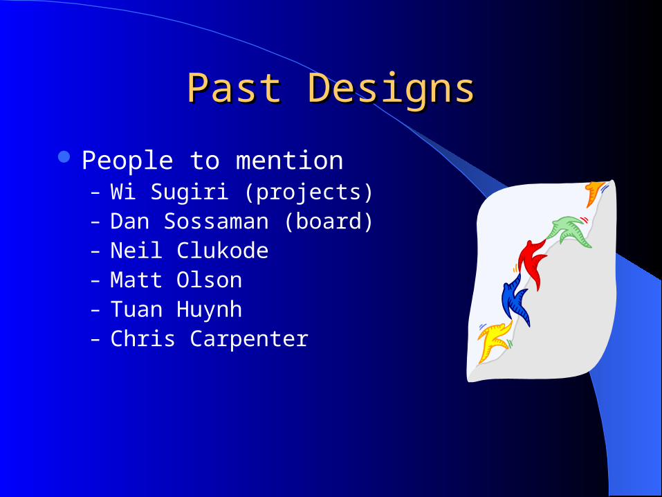
Problems EncounteredProblems Encountered
Issues with new microcontrollers– Chip burners– Capacitance– Internal Fuse Bits
In-System-Programming Circuit

In-System-ProgrammingIn-System-Programming
Modification of the board is possible– Buffer chip– Programmable logic device– Re-wire
Programmable Logic Device
Pin 8Pin 20
RJ45 Jack
Pin 8
Pin 19

In-System-ProgrammingIn-System-Programming
ISP Cable– DB25 to RJ45

ResultsResults

CompletionCompletion
Board applied in the classroomUpdate from previous designsCapable of future updates

Future DesignFuture Design
Reduction of ComponentsDual MicrocontrollersUSBSurface Mount Components

QuestionsQuestions
ReferencesReferences
Marcus O. Durham, PhD. Systems Design and the 8051. Second Edition. TechnoPress. Tulsa, OK. 2003 – 2004.
Altium – Protel http://www.4pcb.com http://www.allelectronics.com http://www.play-hookey.com/digital/experiments
/seven_seg_led.html