Embed Size (px)
Citation preview
UNIT - I: COMPUTER ARITHMETIC, REGISTER TRANSFER LANGUAGE &
MICROOPERATIONS
(09 periods)
Computer Arithmetic: Data Representation, Fixed Point Representation, Floating
Point Representation, Addition and subtraction, Binary multiplication Algorithms,
Binary Division Algorithms, Floating point Arithmetic operations.
Register Transfer Language And Microoperations: Register Transfer,Bus and
memory transfers, Arithmetic Microoperations, Logic microoperations, Shift micro
operations, Arithmetic logic shift unit.
1.1 DATA Representation:
1.1.1 Data Types
• Registers contain either data or control information • Control information is a bit or group of bits used to specify the sequence
of command signals needed for data manipulation • Data are numbers and other binary-coded information that are operated on • Possible data types in registers:
o Numbers used in computations
o Letters of the alphabet used in data processing o Other discrete symbols used for specific purposes
• All types of data, except binary numbers, are represented in binary-coded form
• A number system of base, or radix, r is a system that uses distinct symbols for r
digits
• Numbers are represented by a string of digit symbols • The string of digits 724.5 represents the quantity
7 x 10² + 2 x 10
1 + 4 x 10
0 + 5 x 10
-1
• The string of digits 101101 in the binary number system represents the quantity
1 x 25 + 0 x 2
4 + 1 x 2
3 + 1 x 2
2 + 0 x 2
1 + 1 x 2
0 = 45
• (101101)2 = (45)10 • We will also use the octal (radix 8) and hexadecimal (radix 16) number systems
(736.4)8 = 7 x 82 + 3 x 8
1 + 6 x 8
0 + 4 x 8
-1 = (478.5)10
(F3)16 = F x 161 + 3 x 16
0 = (243)10
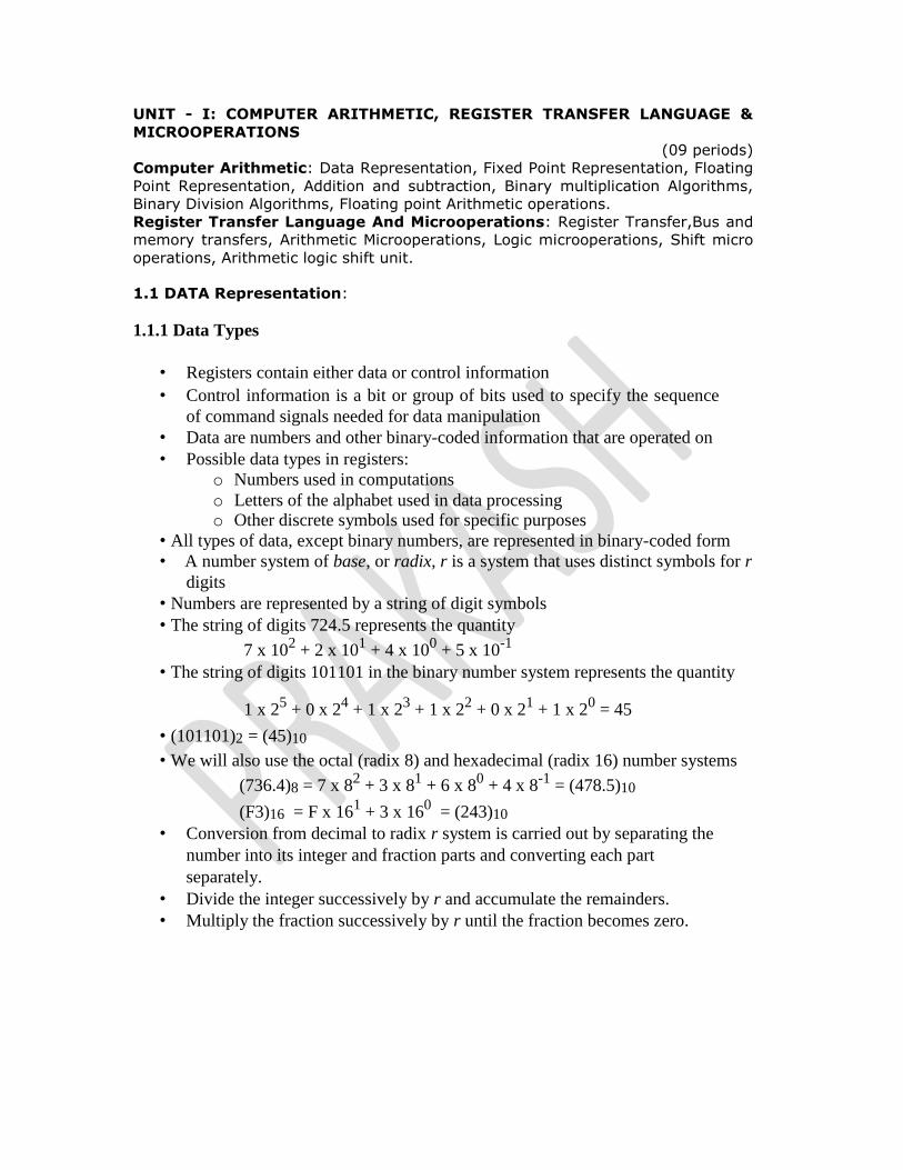
• Conversion from decimal to radix r system is carried out by separating the
number into its integer and fraction parts and converting each part
separately. • Divide the integer successively by r and accumulate the remainders. • Multiply the fraction successively by r until the fraction becomes zero.
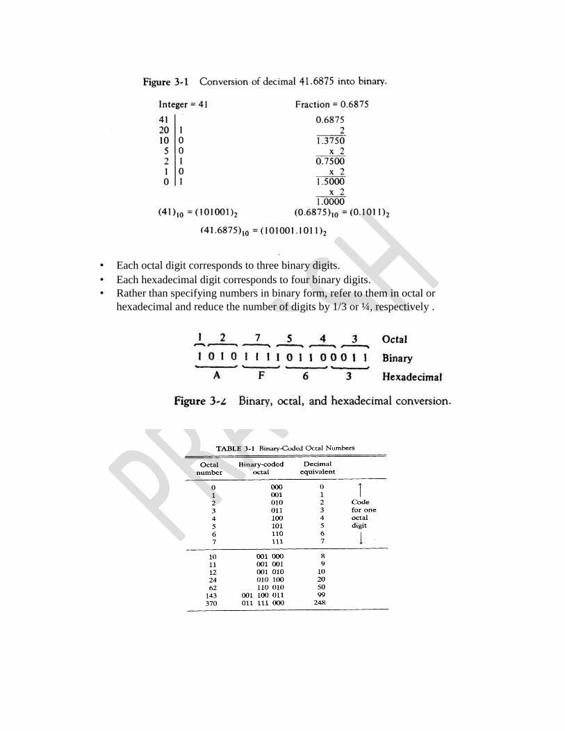
• Each octal digit corresponds to three binary digits. • Each hexadecimal digit corresponds to four binary digits. • Rather than specifying numbers in binary form, refer to them in octal or
hexadecimal and reduce the number of digits by 1/3 or ¼, respectively .

• A binary code is a group of n bits that assume up to 2n distinct combinations
• A four bit code is necessary to represent the ten decimal digits – 6 are unused • The most popular decimal code is called binary-coded decimal (BCD) • BCD is different from converting a decimal number to binary • For example 99, when converted to binary, is 1100011 • 99 when represented in BCD is 1001 1001
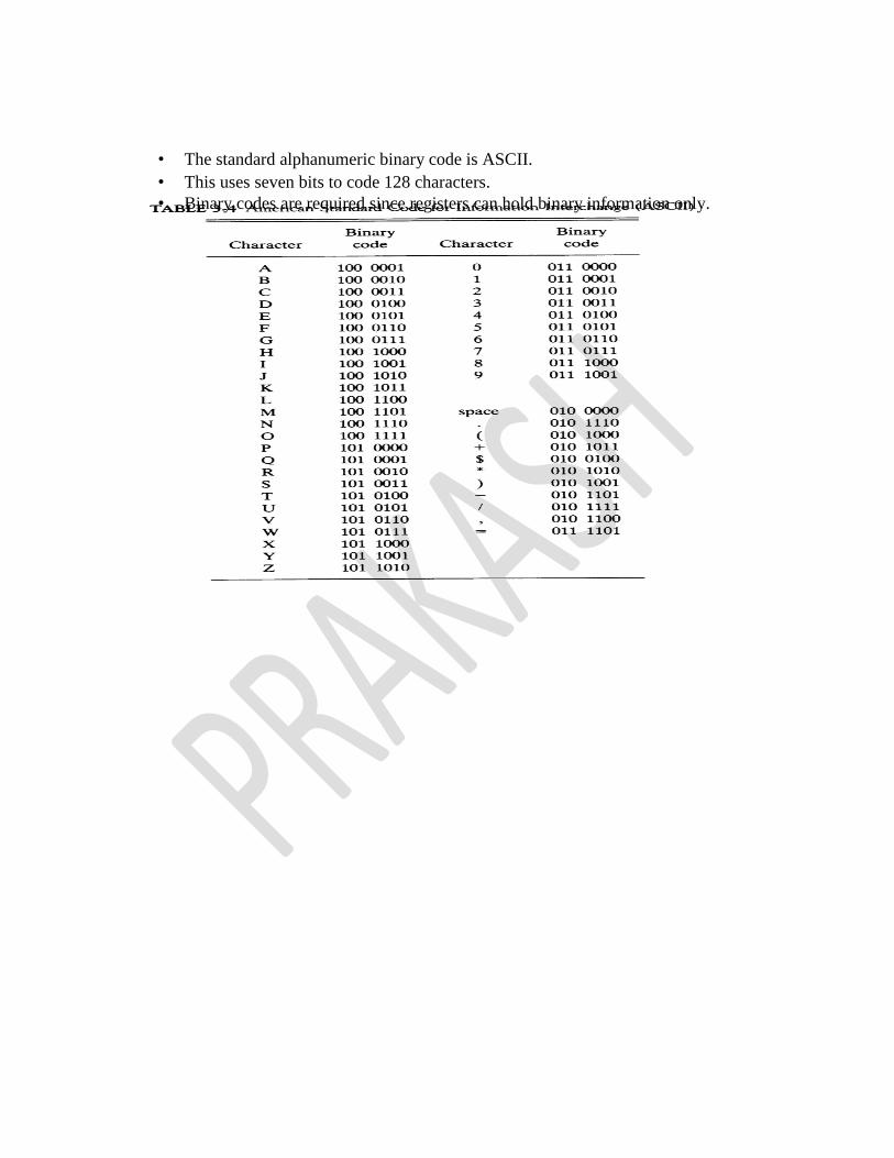
• The standard alphanumeric binary code is ASCII. • This uses seven bits to code 128 characters. • Binary codes are required since registers can hold binary information only.
1.1.2 – Complements
• Complements are used in digital computers for simplifying subtraction and logical
manipulation • Two types of complements for each base r system: r’s complement and (r – 1)’s
complement
• Given a number N in base r having n digits, the (r – 1)’s complement of N is
defined as (rn – 1) – N
• For decimal, the 9’s complement of N is (10n – 1) – N
• The 9’s complement of 546700 is 999999 – 546700 = 453299 • The 9’s complement of 453299 is 999999 – 453299 = 546700 • For binary, the 1’s complement of N is (2
n – 1) – N
• The 1’s complement of 1011001 is 1111111 – 1011001 = 0100110 • The 1’s complement is the true complement of the number – just toggle all bits
• The r’s complement of an n-digit number N in base r is defined as rn – N
• This is the same as adding 1 to the (r – 1)’s complement • The 10’s complement of 2389 is 7610 + 1 = 7611 • The 2’s complement of 101100 is 010011 + 1 = 010100
• Subtraction of unsigned n-digit numbers: M – N
o Add M to the r’s complement of N – this results in
M + (rn – N) = M – N + r
n
o If M ≥ N, the sum will produce an end carry rn which is discarded
o If M < N, the sum does not produce an end carry and is equal to
rn – (N – M), which is the r’s complement of (N – M). To obtain the answer in a
familiar form, take the r’s complement of the sum and place a negative sign in front.
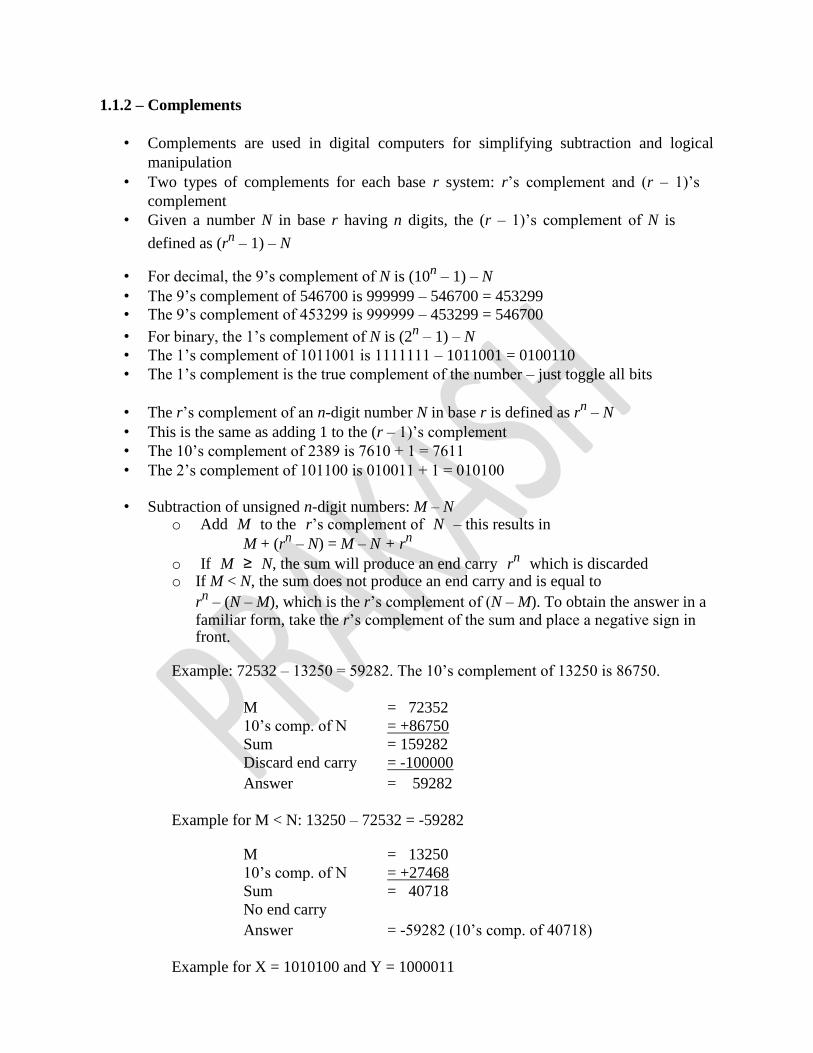
Example: 72532 – 13250 = 59282. The 10’s complement of 13250 is 86750.
M = 72352
10’s comp. of N = +86750
Sum = 159282
Discard end carry = -100000
Answer = 59282
Example for M < N: 13250 – 72532 = -59282
M = 13250
10’s comp. of N = +27468
Sum = 40718
No end carry
Answer = -59282 (10’s comp. of 40718)
Example for X = 1010100 and Y = 1000011
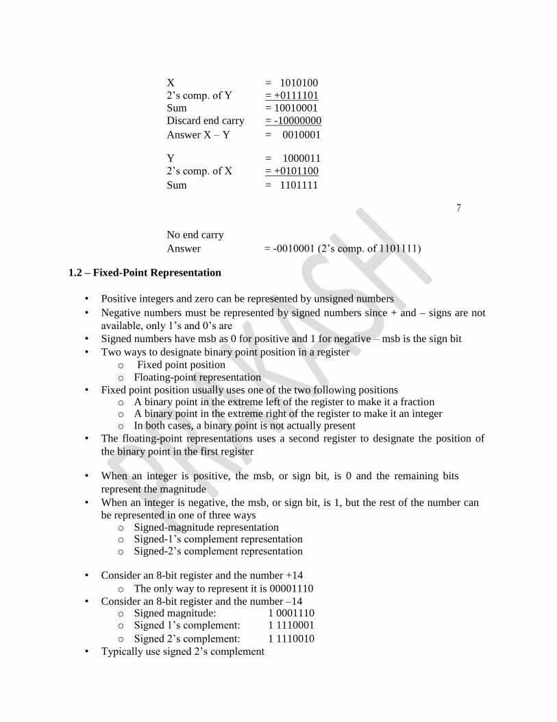
X = 1010100
2’s comp. of Y = +0111101
Sum = 10010001
Discard end carry = -10000000
Answer X – Y = 0010001
Y = 1000011
2’s comp. of X = +0101100
Sum = 1101111
7
No end carry Answer = -0010001 (2’s comp. of 1101111)
1.2 – Fixed-Point Representation
• Positive integers and zero can be represented by unsigned numbers • Negative numbers must be represented by signed numbers since + and – signs are not
available, only 1’s and 0’s are • Signed numbers have msb as 0 for positive and 1 for negative – msb is the sign bit • Two ways to designate binary point position in a register
o Fixed point position
o Floating-point representation • Fixed point position usually uses one of the two following positions
o A binary point in the extreme left of the register to make it a fraction o A binary point in the extreme right of the register to make it an integer o In both cases, a binary point is not actually present
• The floating-point representations uses a second register to designate the position of
the binary point in the first register
• When an integer is positive, the msb, or sign bit, is 0 and the remaining bits
represent the magnitude • When an integer is negative, the msb, or sign bit, is 1, but the rest of the number can
be represented in one of three ways o Signed-magnitude representation o Signed-1’s complement representation o Signed-2’s complement representation
• Consider an 8-bit register and the number +14 o The only way to represent it is 00001110
• Consider an 8-bit register and the number –14 o Signed magnitude: 1 0001110 o Signed 1’s complement: 1 1110001
o Signed 2’s complement: 1 1110010 • Typically use signed 2’s complement
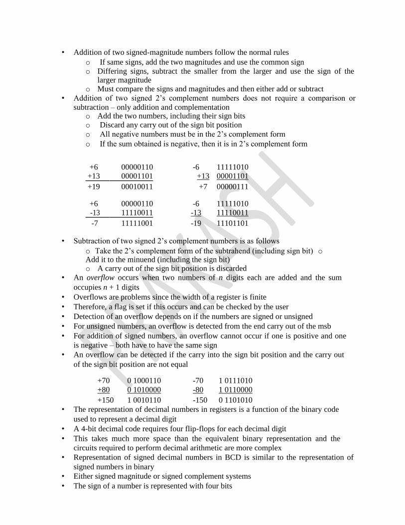
• Addition of two signed-magnitude numbers follow the normal rules o If same signs, add the two magnitudes and use the common sign
o Differing signs, subtract the smaller from the larger and use the sign of the larger magnitude
o Must compare the signs and magnitudes and then either add or subtract • Addition of two signed 2’s complement numbers does not require a comparison or
subtraction – only addition and complementation o Add the two numbers, including their sign bits o Discard any carry out of the sign bit position
o All negative numbers must be in the 2’s complement form
o If the sum obtained is negative, then it is in 2’s complement form
+6 00000110 -6 11111010 +13 00001101 +13 00001101
+19 00010011 +7 00000111
+6 00000110 -6 11111010 -13 11110011 -13 11110011
-7 11111001 -19 11101101
• Subtraction of two signed 2’s complement numbers is as follows o Take the 2’s complement form of the subtrahend (including sign bit) o Add it to the minuend (including the sign bit) o A carry out of the sign bit position is discarded
• An overflow occurs when two numbers of n digits each are added and the sum
occupies n + 1 digits
• Overflows are problems since the width of a register is finite • Therefore, a flag is set if this occurs and can be checked by the user • Detection of an overflow depends on if the numbers are signed or unsigned • For unsigned numbers, an overflow is detected from the end carry out of the msb • For addition of signed numbers, an overflow cannot occur if one is positive and one
is negative – both have to have the same sign • An overflow can be detected if the carry into the sign bit position and the carry out
of the sign bit position are not equal
+70 0 1000110 -70 1 0111010
+80 0 1010000 -80 1 0110000
+150 1 0010110 -150 0 1101010
• The representation of decimal numbers in registers is a function of the binary code
used to represent a decimal digit
• A 4-bit decimal code requires four flip-flops for each decimal digit • This takes much more space than the equivalent binary representation and the
circuits required to perform decimal arithmetic are more complex
• Representation of signed decimal numbers in BCD is similar to the representation of
signed numbers in binary
• Either signed magnitude or signed complement systems • The sign of a number is represented with four bits
o 0000 for +
o 1001 for – • To obtain the 10’s complement of a BCD number, first take the 9’s complement and
then add one to the least significant digit
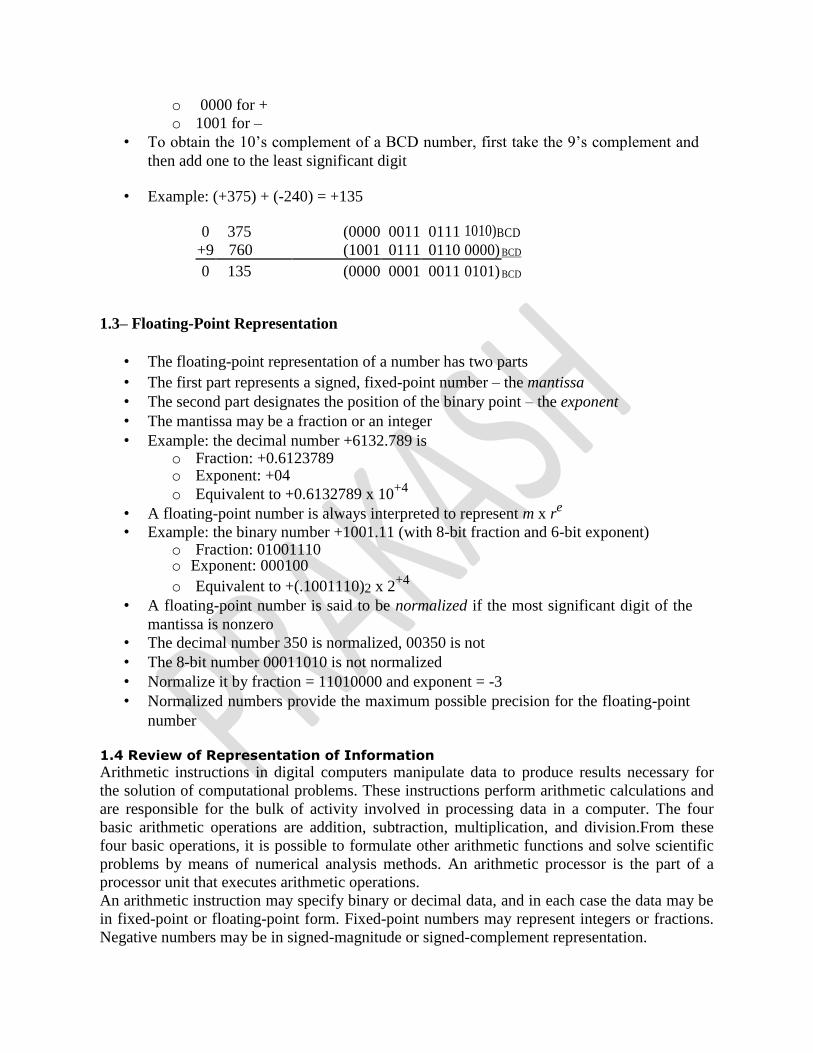
• Example: (+375) + (-240) = +135
0 375 (0000 0011 0111 1010)BCD
+9 760 (1001 0111 0110 0000) BCD
0 135 (0000 0001 0011 0101) BCD
1.3– Floating-Point Representation
• The floating-point representation of a number has two parts • The first part represents a signed, fixed-point number – the mantissa • The second part designates the position of the binary point – the exponent • The mantissa may be a fraction or an integer • Example: the decimal number +6132.789 is
o Fraction: +0.6123789 o Exponent: +04
o Equivalent to +0.6132789 x 10+4
• A floating-point number is always interpreted to represent m x re
• Example: the binary number +1001.11 (with 8-bit fraction and 6-bit exponent) o Fraction: 01001110 o Exponent: 000100
o Equivalent to +(.1001110)2 x 2+4
• A floating-point number is said to be normalized if the most significant digit of the
mantissa is nonzero • The decimal number 350 is normalized, 00350 is not • The 8-bit number 00011010 is not normalized • Normalize it by fraction = 11010000 and exponent = -3 • Normalized numbers provide the maximum possible precision for the floating-point
number
1.4 Review of Representation of Information
Arithmetic instructions in digital computers manipulate data to produce results necessary for
the solution of computational problems. These instructions perform arithmetic calculations and
are responsible for the bulk of activity involved in processing data in a computer. The four
basic arithmetic operations are addition, subtraction, multiplication, and division.From these
four basic operations, it is possible to formulate other arithmetic functions and solve scientific
problems by means of numerical analysis methods. An arithmetic processor is the part of a
processor unit that executes arithmetic operations.
An arithmetic instruction may specify binary or decimal data, and in each case the data may be
in fixed-point or floating-point form. Fixed-point numbers may represent integers or fractions.
Negative numbers may be in signed-magnitude or signed-complement representation.
At an early age we are taught how to perform the basic arithmetic operations in signed-
magnitude representation. . We consider addition, subtraction, multiplication, and division for
the following types of data:
1. Fixed-point binary data in signed-magnitude representation
2. Fixed-point binary data in signed-2’s complement representation
3. Floating-point binary data
4. Binary-coded decimal (BCD) data
Addition and Subtraction
There are three ways of representing negative fixed-point binary numbers: signed-
magnitude, signed-1's complement, or signed-2's complement. Most computers use the
signed-2's complement representation when performing arithmetic operations with
integers. For floating-point operations, most computers use the signed-magnitude
representation for the mantissa.
Addition and Subtraction with Signed-Magnitude Data
The representation of numbers in signed-magnitude is familiar because it is used in
everyday arithmetic calculations. The procedure for adding or subtracting two signed
binary numbers with paper and pencil is simple and straight-forward. A review of this
procedure will be helpful for deriving the hardware algorithm. We designate the magnitude
of the two numbers by A and B . When the signed numbers are added or subtracted, we
find that there are eight different conditions to consider, depending on the sign of the
numbers and the operation performed.
These conditions are listed in the first column of Table 10-1. The other columns in the
table show the actual operation to be performed with the magnitude of the numbers. The
algorithms for addition and subtraction are derived from the table and can be stated as
follows (the words inside parentheses should be used for the subtraction algorithm):
Addition (subtraction) algorithm: when the signs of A and B are identical (different), add
the two magnitudes and attach the sign of A to the result. When the signs of A and B are
different (identical), compare the magnitudes and subtract the smaller number from the
larger. Choose the sign of the result to be the same as A if A > B or the complement of the
sign of A if A < B. If the two magnitudes are equal, subtract B from A and make the sign of
the result positive. The two algorithms are similar except for the sign comparison. The
procedure to be followed for identical signs in the addition algorithm is the same as for
different signs in the subtraction algorithm, and vice versa.

Hardware Implementation
To implement the two arithmetic operations with hardware, it is first necessary that the
two numbers be stored in registers. Let A and B be two registers that hold the magnitudes
of the numbers, and As and Bs be two flip-flops that hold the corresponding signs. The
result of the operation may be transferred to a third register: however, a saving is
achieved if the result is transferred into A and As. Thus A and As together form an
accumulator register. Consider now the hardware implementation of the algorithms above.
Figure 10-1 shows a block diagram of the hardware for implementing the addition and
subtraction operations. It consists of registers A and B and sign flip-flops As, and Bs.
Subtraction is done by adding A to the 2's complement of B. The output carry is
transferred to flip-flop E, where it can be checked to determine the relative magnitudes of
the two numbers. The add-overflow flip-flop AVF holds the overflow bit when A and B are
added. The A register provides other microoperations that may be needed when we specify
the sequence of steps in the algorithm. The addition of A plus B is done through the
parallel adder. The S (sum) output of the adder is applied to the input of the A register.
The complementer provides an output of B or the complement of B depending on the state
of the mode control M. The complementer consists of exclusive-OR gates and the parallel
adder consists of full-adder circuits. The M signal is also applied to the input carry of the
adder. When M = 0, the output of B is transferred to the adder, the input carry is 0, and
the output of the adder is equal to the sum A + B. When M = 1, the l's complement of B is
applied to the adder, the input carry is 1, and output S = A + �̅� + 1. This is equal to A plus
the 2's complement of B, which is equivalent to the subtraction A — B.
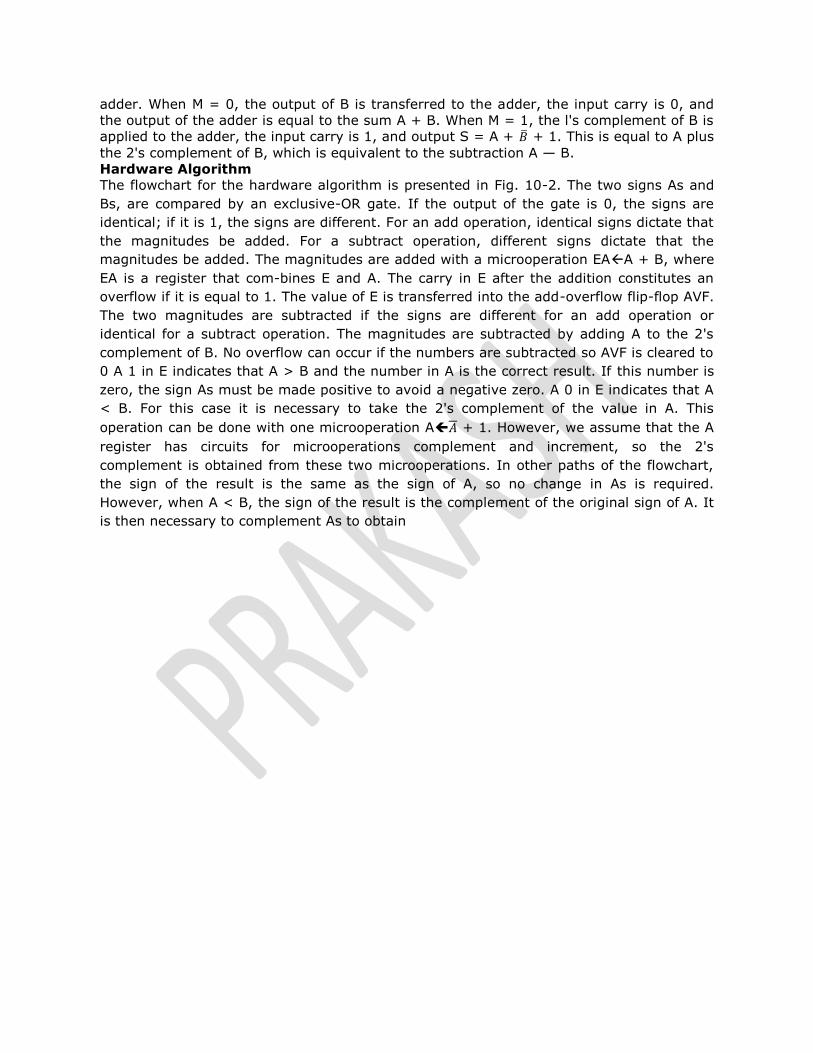
Hardware Algorithm
The flowchart for the hardware algorithm is presented in Fig. 10-2. The two signs As and
Bs, are compared by an exclusive-OR gate. If the output of the gate is 0, the signs are
identical; if it is 1, the signs are different. For an add operation, identical signs dictate that
the magnitudes be added. For a subtract operation, different signs dictate that the
magnitudes be added. The magnitudes are added with a microoperation EAA + B, where
EA is a register that com-bines E and A. The carry in E after the addition constitutes an
overflow if it is equal to 1. The value of E is transferred into the add-overflow flip-flop AVF.
The two magnitudes are subtracted if the signs are different for an add operation or
identical for a subtract operation. The magnitudes are subtracted by adding A to the 2's
complement of B. No overflow can occur if the numbers are subtracted so AVF is cleared to
0 A 1 in E indicates that A > B and the number in A is the correct result. If this number is
zero, the sign As must be made positive to avoid a negative zero. A 0 in E indicates that A
< B. For this case it is necessary to take the 2's complement of the value in A. This
operation can be done with one microoperation A�̅� + 1. However, we assume that the A
register has circuits for microoperations complement and increment, so the 2's
complement is obtained from these two microoperations. In other paths of the flowchart,
the sign of the result is the same as the sign of A, so no change in As is required.
However, when A < B, the sign of the result is the complement of the original sign of A. It
is then necessary to complement As to obtain
the correct sign. The final result is found in register A and its sign in As. The value in AVE
provides an overflow indication. The final value of E is immaterial.
Addition and Subtraction with Signed-2's Complement Data
The addition of two numbers in signed-2's complement form consists of adding the
numbers with the sign bits treated the same as the other bits of the number. A carry-out
of the sign-bit position is discarded. The subtraction consists of first taking the 2's
complement of the subtrahend and then adding it to the minuend. When two numbers of n
digits each are added and the sum occupies n + 1 digits, we say that an overflow occurred.
An overflow can be detected by inspecting the last two carries out of the addition. When
the two carries are applied to an exclusive-OR gate, the overflow is detected when the
output of the gate is equal to 1.
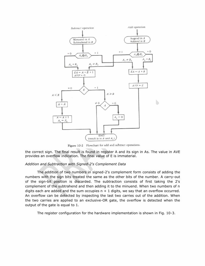
The register configuration for the hardware implementation is shown in Fig. 10-3.
We name the A register AC (accumulator) and the B register BR . The leftmost bit in
AC and BR represent the sign bits of the numbers. The two sign bits are added or
subtracted together with the other bits in the complementer and parallel adder. The
overflow flip-flop V is set to 1 if there is an overflow. The output carry in this case is
discarded.
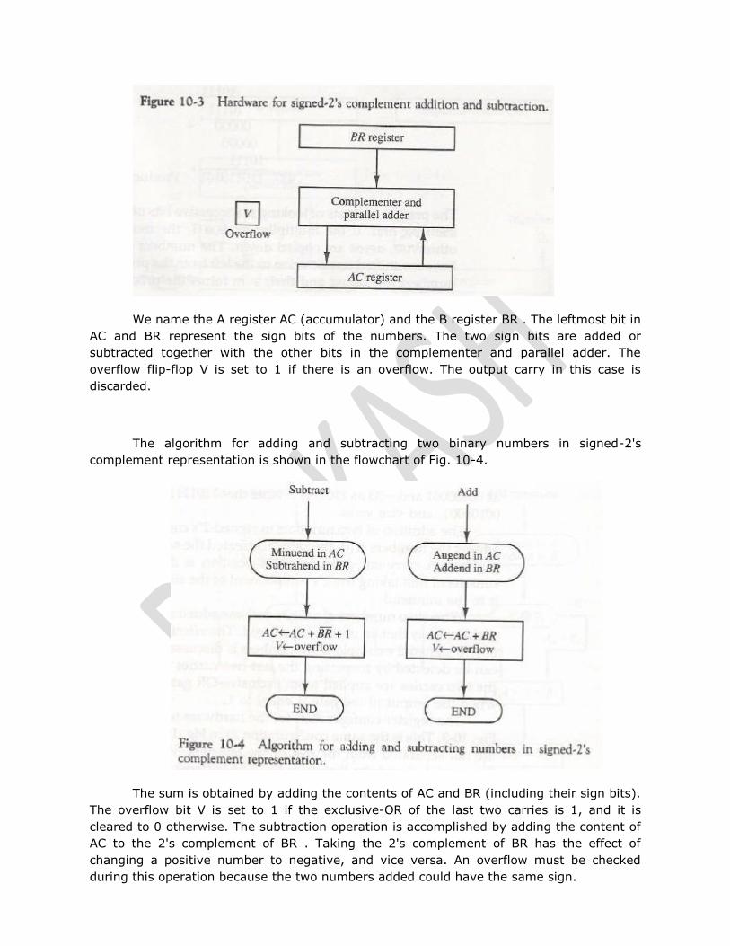
The algorithm for adding and subtracting two binary numbers in signed-2's
complement representation is shown in the flowchart of Fig. 10-4.
The sum is obtained by adding the contents of AC and BR (including their sign bits).
The overflow bit V is set to 1 if the exclusive-OR of the last two carries is 1, and it is
cleared to 0 otherwise. The subtraction operation is accomplished by adding the content of
AC to the 2's complement of BR . Taking the 2's complement of BR has the effect of
changing a positive number to negative, and vice versa. An overflow must be checked
during this operation because the two numbers added could have the same sign.
1.5 Multiplication and Division Algorithms
The process consists of looking at successive bits of the multiplier, least significant
bit first. If the multiplier bit is a 1, the multiplicand is copied down; otherwise, zeros are
copied down. The numbers copied down in successive lines are shifted one position to the
left from the previous number. Finally, the numbers are added and their sum forms the
product.
The sign of the product is determined from the signs of the multiplicand and
multiplier. If they are alike, the sign of the product is positive. If they are unlike, the sign
of the product is negative.
This process is best illustrated with a numerical example.
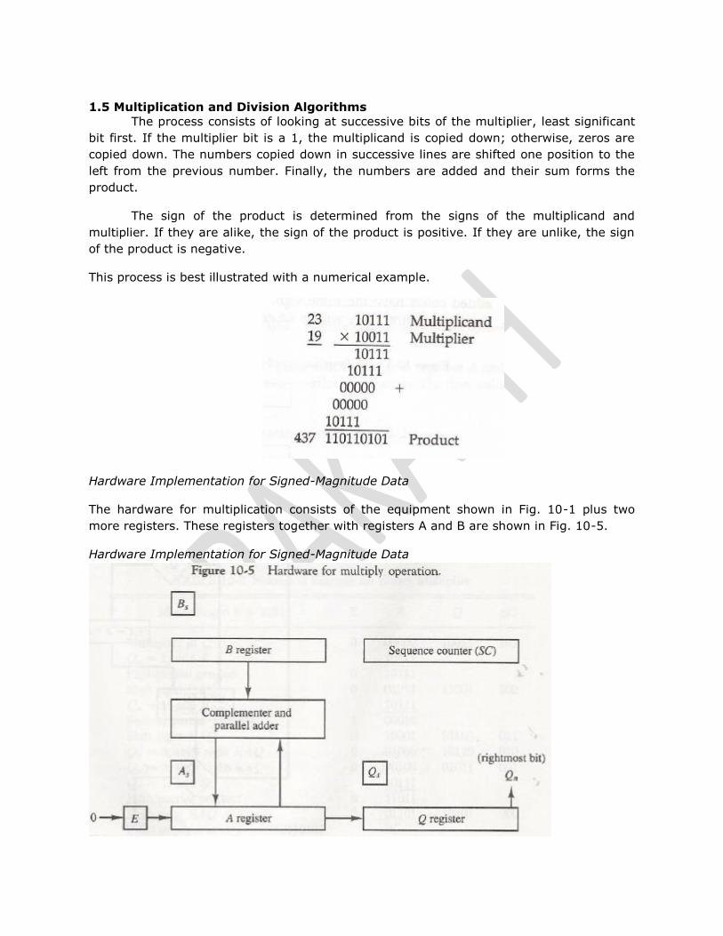
Hardware Implementation for Signed-Magnitude Data
The hardware for multiplication consists of the equipment shown in Fig. 10-1 plus two
more registers. These registers together with registers A and B are shown in Fig. 10-5.
Hardware Implementation for Signed-Magnitude Data
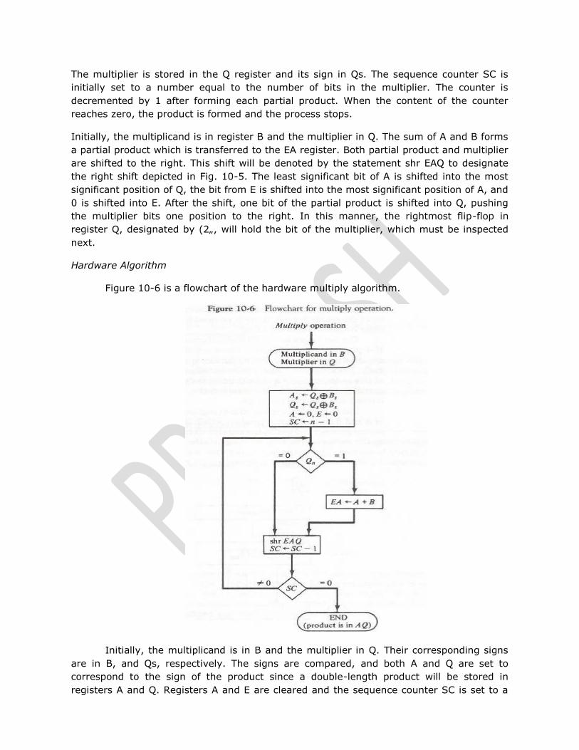
The multiplier is stored in the Q register and its sign in Qs. The sequence counter SC is
initially set to a number equal to the number of bits in the multiplier. The counter is
decremented by 1 after forming each partial product. When the content of the counter
reaches zero, the product is formed and the process stops.
Initially, the multiplicand is in register B and the multiplier in Q. The sum of A and B forms
a partial product which is transferred to the EA register. Both partial product and multiplier
are shifted to the right. This shift will be denoted by the statement shr EAQ to designate
the right shift depicted in Fig. 10-5. The least significant bit of A is shifted into the most
significant position of Q, the bit from E is shifted into the most significant position of A, and
0 is shifted into E. After the shift, one bit of the partial product is shifted into Q, pushing
the multiplier bits one position to the right. In this manner, the rightmost flip-flop in
register Q, designated by (2„, will hold the bit of the multiplier, which must be inspected
next.
Hardware Algorithm
Figure 10-6 is a flowchart of the hardware multiply algorithm.
Initially, the multiplicand is in B and the multiplier in Q. Their corresponding signs
are in B, and Qs, respectively. The signs are compared, and both A and Q are set to
correspond to the sign of the product since a double-length product will be stored in
registers A and Q. Registers A and E are cleared and the sequence counter SC is set to a

number equal to the number of bits of the multiplier. We are assuming here that operands
are transferred to registers from a memory unit that has words of n bits. Since an operand
must be stored with its sign, one bit of the word will be occupied by the sign and the
magnitude will consist of n — 1 bits. After the initialization, the low-order bit of the
multiplier in Qn is tested. If it is a 1, the multiplicand in B is added to the present partial
product in A . If it is a 0, nothing is done. Register EAQ is then shifted once to the right to
form the new partial product. The sequence counter is decremented by 1 and its new value
checked. If it is not equal to zero, the process is repeated and a new partial product is
formed. The process stops when SC = 0. Note that the partial product formed in A is
shifted into Q one bit at a time and eventually replaces the multiplier. The final product is
available in both A and Q, with A holding the most significant bits and Q holding the least
significant bits.
Booth Multiplication Algorithm
Booth algorithm gives a procedure for multiplying binary integers in signed-2's
complement representation. It operates on the fact that strings of 0's in the multiplier
require no addition but just shifting, and a string of 1's in the multiplier from bit weight 2k
to weight 2m can be treated as 2k+1 — 2m.
For example, the binary number 001110 (+14) has a string of l's from 23 to 21 k = 3, in =
1). The number can be represented as 2 k+1 — 2m = 24 — 21 = 16 —2 = 14. Therefore, the
multiplication M x 14, where M is the multiplicand and 14 the multiplier, can be done as M
x 24 — M x 21. Thus the product can be obtained by shifting the binary multiplicand M four
times to the left and subtracting M shifted left once. As in all multiplication schemes, Booth
algorithm requires examination of the multiplier bits and shifting of the partial product.
Prior to the shifting, the multiplicand may be added to the partial product, subtracted from
the partial product, or left unchanged according to the following rules:
1. The multiplicand is subtracted from the partial product upon encountering the first least
significant 1 in a string of 1's in the multiplier.
2. The multiplicand is added to the partial product upon encountering the first 0 (provided
that there was a previous 1) in a string of 0's in the multiplier.
3. The partial product does not change when the multiplier bit is identical to the previous
multiplier bit.
The algorithm works for positive or negative multipliers in 2's complement representation.
This is because a negative multiplier ends with a string of l's and the last operation will be
a subtraction of the appropriate weight. For example, a multiplier equal to —14 is
represented in 2's complement as 110010 and is treated as —24- 22 — 21 = —14.
The hardware implementation of Booth algorithm
The hardware implementation of Booth algorithm requires the register configuration shown
in Fig. 10-7. To show this difference, we rename registers A, B, and Q, as AC, BR, and QR,
respectively. Qn, designates the least significant bit of the multiplier in register QR. An
extra flip-flop Qn+1 is appended to QR to facilitate a double bit inspection of the multiplier.
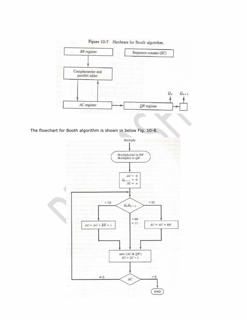
The flowchart for Booth algorithm is shown in below Fig. 10-8.
AC and the appended bit are initially cleared to 0 and the sequence counter SC is set to a
number n equal to the number of bits in the multiplier. The two bits of the multiplier in Qn
andQn+1 are inspected. If the two bits are equal to 10, it means that the first 1 in a string
of 1's has been encountered. This requires a subtraction of the multiplicand from the
partial product in AC. If the two bits are equal to 01, it means that the first 0 in a string of
0's has been encountered. This requires the addition of the multiplicand to the partial
product in AC. When the two bits are equal, the partial product does not change. An
overflow cannot occur because the addition and subtraction of the multiplicand follow each
other. As a consequence, the two numbers that are added always have opposite signs, a
condition that excludes an overflow. The next step is to shift right the partial product and
the multiplier (including bit Qn+1). This is an arithmetic shift right (ashr) operation which
shifts AC and QR to the right and leaves the sign bit in AC unchanged. The sequence
counter is decremented and the computational loop is repeated n times.
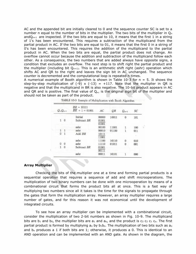
A numerical example of Booth algorithm is shown in Table 10-3 for n = 5. It shows the
step-by-step multiplication of (-9) x (-13) = +117. Note that the multiplier in QR is
negative and that the multiplicand in BR is also negative. The 10-bit product appears in AC
and QR and is positive. The final value of Q„, is the original sign bit of the multiplier and
should not be taken as part of the product.
Array Multiplier
Checking the bits of the multiplier one at a time and forming partial products is a
sequential operation that requires a sequence of add and shift microoperations. The
multiplication of two binary numbers can be done with one microoperation by means of a
combinational circuit that forms the product bits all at once. This is a fast way of
multiplying two numbers since all it takes is the time for the signals to propagate through
the gates that form the multiplication array. However, an array multiplier requires a large
number of gates, and for this reason it was not economical until the development of
integrated circuits.
To see how an array multiplier can be implemented with a combinational circuit,
consider the multiplication of two 2-bit numbers as shown in Fig. 10-9. The multiplicand
bits are b1 and b0, the multiplier bits are a1 and ao, and the product is c3 c2 c1 co. The first
partial product is formed by multiplying ao by b1bo. The multiplication of two bits such as ao
and bo produces a 1 if both bits are 1; otherwise, it produces a 0. This is identical to an
AND operation and can be implemented with an AND gate. As shown in the diagram, the
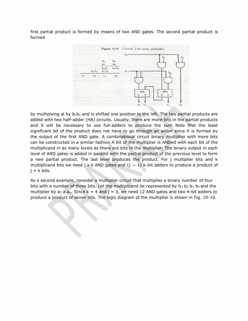
first partial product is formed by means of two AND gates. The second partial product is
formed
by multiplying al by b1bo and is shifted one position to the left. The two partial products are
added with two half-adder (HA) circuits. Usually, there are more bits in the partial products
and it will be necessary to use full-adders to produce the sum Note that the least
significant bit of the product does not have to go through an adder since it is formed by
the output of the first AND gate. A combinational circuit binary multiplier with more bits
can be constructed in a similar fashion A bit of the multiplier is ANDed with each bit of the
multiplicand in as many levels as there are bits in the multiplier. The binary output in each
level of AND gates is added in parallel with the partial product of the previous level to form
a new partial product. The last level produces the product. For j multiplier bits and k
multiplicand bits we need j x k AND gates and (j — 1) k-bit adders to produce a product of
j + k bits.
As a second example, consider a multiplier circuit that multiplies a binary number of four
bits with a number of three bits. Let the multiplicand be represented by b3 b2 b1 b0 and the
multiplier by a2 a1ao. Since k = 4 and j = 3, we need 12 AND gates and two 4-bit adders to
produce a product of seven bits. The logic diagram of the multiplier is shown in Fig. 10-10.
1.6 Division Algorithms
The division process is illustrated by a numerical example in Fig. 10-11.
The divisor B consists of five bits and the dividend A, of ten bits. The five most significant
bits of the dividend are compared with the divisor. Since the 5-bit number is smaller than
B, we try again by taking the six most significant bits of A and compare this number with
B. The 6-bit number is greater than B, so we place a 1 for the quotient bit in the sixth
position above the dividend. The divisor is then shifted once to the right and subtracted
from the dividend. The difference is called a partial remainder because the division could
have stopped here to obtain a quotient of 1 and a remainder equal to the partial
remainder. The process is continued by comparing a partial remainder with the divisor. If
the partial remainder is greater than or equal to the divisor, the quotient bit is equal to 1.
The divisor is then shifted right and subtracted from the partial remainder. If the partial
remainder is smaller than the divisor, the quotient bit is 0 and no subtraction is needed.

The divisor is shifted once to the right in any case. Note that the result gives both a
quotient and a remainder.
Hardware Implementation for Signed-Magnitude Data
The hardware for implementing the division operation is identical to that required for
multiplication and consists of the components shown in Fig. 10-5. Register EAQ is now
shifted to the left with 0 inserted into Q„ and the previous value of E lost. The numerical
example is repeated in Fig. 10-12 to clarify the proposed division process. The divisor is
stored in the B register and the double-length dividend is stored in registers A and Q. The
dividend is shifted to the left and the divisor is subtracted by adding its 2's complement
value. The information about the relative magnitude is available in E. If E = 1, it signifies
that A ≥B. A quotient bit 1 is inserted into Qn and the partial remainder is shifted to the
left to repeat the process. If E = 0, it signifies that A < B so the quotient in Qn remains a 0
(inserted during the shift). The value of B is then added to restore the partial remainder in
A to its previous value. The partial remainder is shifted to the left and the process is
repeated again until all five quotient bits are formed. Note that while the partial remainder
is shifted left, the quotient bits are shifted also and after five shifts, the quotient is in Q
and the final remainder is in A.
Before showing the algorithm in flowchart form, we have to consider the sign of the result
and a possible overflow condition.

The sign of the quotient is determined from the signs of the dividend and the divisor. If the
two signs are alike, the sign of the quotient is plus. If they are unalike, the sign is minus.
The sign of the remainder is the same as the sign of the dividend.
Divide Overflow
When the dividend is twice as long as the divisor, the condition for overflow can be
stated as follows: A divide-overflow condition occurs if the high-order half bits of the
dividend constitute a number greater than or equal to the divisor. Another problem
associated with division is the fact that a division by zero must be avoided. The divide-
overflow condition takes care of this condition as well. This occurs because any dividend
will be greater than or equal to a divisor which is equal to zero. Overflow condition is
usually detected when a special flip-flop is set. We will call it a divide-overflow flip-flop and
label it DVF.
The occurrence of a divide overflow can be handled in a variety of ways. In some
computers it is the responsibility of the programmers to check if DVF is set after each
divide instruction. They then can branch to a subroutine that takes a corrective measure
such as resealing the data to avoid overflow. In some older computers, the occurrence of a
divide overflow stopped the computer and this condition was referred to as a divide stop.
Stopping the operation of the computer is not recommended because it is time consuming.
The procedure in most computers is to provide an interrupt request when DVF is set. The
interrupt causes the computer to suspend the current program and branch to a service
routine to take a corrective measure. The most common corrective measure is to remove
the program and type an error message explaining the reason why the program could not
be completed. It is then the responsibility of the user who wrote the program to rescale
the data or take any other corrective measure. The best way to avoid a divide overflow is
to use floating-point data.
Hardware Algorithm
Hardware Algorithm The hardware divide algorithm is shown in the flowchart of Fig. 10-13.
The dividend is in A and Q and the divisor in B . The sign of the result is transferred into Q,
to be part of the quotient. A constant is set into the sequence counter SC to specify the
number of bits in the quotient. As in multiplication, we assume that operands are
transferred to registers from a memory unit that has words of n bits. Since an operand
must be stored with its sign, one bit of the word will be occupied by the sign and the
magnitude will consist of n-1 bits.
A divide-overflow condition is tested by subtracting the divisor in B from half of the bits of
the dividend stored in A. If A ≥ B, the divide-overflow flip-flop DVF is set and the operation
is terminated prematurely. If A < B, no divide overflow occurs so the value of the dividend
is restored by adding B to A. The division of the magnitudes starts by shifting the dividend
in AQ to the left with the high-order bit shifted into E. If the bit shifted into E is 1, we know
that EA > B because EA consists of a 1 followed by n —1 bits while B consists of only n —1
bits. In this case, B must be subtracted from EA and 1 inserted into Qn, for the quotient
bit. Since register A is missing the high-order bit of the dividend (which is in E), its value is
EA — 2n-1. Adding to this value the 2's complement of B results in
(EA — 2n-1) + (2n-1 - B) = EA — B
The carry from this addition is not transferred to E if we want E to remain a 1.
If the shift-left operation inserts a 0 into E, the divisor is subtracted by adding its 2's
complement value and the carry is transferred into E If E = 1, it signifies that A ≥ B;
therefore, Q„ is set to 1. If E = 0, it signifies that A < B and the original number is restored
by adding B to A. In the latter case we leave a 0 in Qn, (0 was inserted during the shift).
This process is repeated again with register A holding the partial remainder. After n — 1
times, the quotient magnitude is formed in register Q and the remainder is found in
register A. The quotient sign is in Qs and the sign of the remainder in As is the same as the
original sign of the dividend.
1.7 Floating-Point Arithmetic Operation
Register Configuration
The register configuration for floating-point operations is quite similar to the layout for
fixed-point operations. As a general rule, the same registers and adder used for fixed-point
arithmetic are used for processing the mantissas. The difference lies in the way the
exponents are handled.
The register organization for floating-point operations is shown in Fig. 10-14. There are
three registers, BR, AC, and QR. Each register is subdivided into two parts. The mantissa
part has the same uppercase letter symbols as in fixed-point representation. The exponent
part uses the corresponding lower-case letter symbol.
It is assumed that each floating-point number has a mantissa in signed-magnitude
representation and a biased exponent. Thus the AC has a mantissa whose sign is in As, and
a magnitude that is in A . The exponent is in the part of the register denoted by the
lowercase letter symbol a. The diagram shows explicitly the most significant bit of A,
labeled by A1. The bit in this position must be a 1 for the number to be normalized. Note
that the symbol AC represents the entire register, that is, the concatenation of As, A, and
a.
Similarly, register BR is subdivided into Bs B, and b, and QR into Qs, Q, and q. A parallel-
adder adds the two mantissas and transfers the sum into A and the carry into E. A
separate parallel-adder is used for the exponents. Since the exponents are biased, they do
not have a distinct sign bit but are represented as a biased positive quantity. It is assumed
that the floating-point numbers are so large that the chance of an exponent overflow is
very remote, and for this reason the exponent overflow will be neglected. The exponents
are also connected to a magnitude comparator that provides three binary outputs to
indicate their relative magnitude. The number in the mantissa will be taken as a fraction,
so the binary point is assumed to reside to the left of the magnitude part. Integer
representation for floating-point causes certain scaling problems during multiplication and

division. To avoid these problems, we adopt a fraction representation. The numbers in the
registers are assumed to be initially normalized. After each arithmetic operation, the result
will be normalized. Thus all floating-point operands coming from and going to the memory
unit are always normalized.
Addition and Subtraction
During addition or subtraction, the two floating-point operands are in AC and BR. The sum
or difference is formed in the AC. The algorithm can be divided into four consecutive parts:
1. Check for zeros.
2. Align the mantissas.
3. Add or subtract the mantissas.
4. Normalize the result.
A floating-point number that is zero cannot be normalized. If this number is used during
the computation, the result may also be zero. Instead of checking for zeros during the
normalization process we check for zeros at the beginning and terminate the process if
necessary. The alignment of the mantissas must be carried out prior to their operation.
After the mantissas are added or subtracted, the result may be unnormalized. The
normalization procedure ensures that the result is normalized prior to its transfer to
memory.
The flowchart for adding or subtracting two floating-point binary numbers is shown in Fig.
10-15. If BR is equal to zero, the operation is terminated, with the value in the AC being
the result. If AC is equal to zero, we transfer the content of BR into AC and also
complement its sign if the numbers are to be subtracted. If neither number is equal to
zero, we proceed to align the mantissas. The magnitude comparator attached to exponents
a and b provides three outputs that indicate their relative magnitude. If the two exponents
are equal, we go to perform the arithmetic operation. If the exponents are not equal, the
mantissa having the smaller exponent is shifted to the right and its exponent incremented.
This process is repeated until the two exponents are equal.
The addition and subtraction of the two mantissas is identical to the fixed-point addition
and subtraction algorithm presented in Fig. 10-2. The magnitude part is added or
subtracted depending on the operation and the signs of the two mantissas. If an overflow
occurs when the magnitudes are added, it is transferred into flip-flop E. If E is equal to 1,
the bit is transferred into A1 and all other bits of A are shifted right. The exponent must be
incremented to maintain the correct number. No underflow may occur in this case because
the original mantissa that was not shifted during the alignment was already in a
normalized position
If the magnitudes were subtracted, the result may be zero or may have an underflow. If
the mantissa is zero, the entire floating-point number in the AC is made zero. Otherwise,
the mantissa must have at least one bit that is equal to 1. The mantissa has an underflow
if the most significant bit in position A1 is 0. In that case, the mantissa is shifted left and
the exponent decremented. The bit in A1 is checked again and the process is repeated until
it is equal to 1. When A1 = 1, the mantissa is normalized and the operation is completed.
Multiplication
The multiplication of two floating-point numbers requires that we multiply the mantissas
and add the exponents No comparison of exponents or alignment of mantissas is
necessary. The multiplication of the mantissas is performed in the same way as in fixed-
point to provide a double-precision product. The double-precision answer is used in fixed-
point numbers to increase the accuracy of the product. In floating-point, the range of a
single-precision mantissa combined with the exponent is usually accurate enough so that
only single-precision numbers are maintained. Thus the half most significant bits of the
mantissa product and the exponent will be taken together to form a single-precision
floating-point product. The multiplication algorithm can be subdivided into four parts:
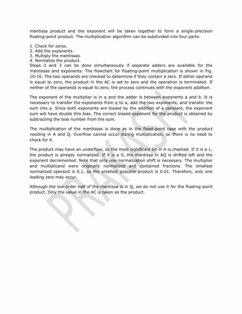
1. Check for zeros.
2. Add the exponents.
3. Multiply the mantissas.
4. Normalize the product.
Steps 2 and 3 can be done simultaneously if separate adders are available for the
mantissas and exponents. The flowchart for floating-point multiplication is shown in Fig.
10-16. The two operands are checked to determine if they contain a zero. If either operand
is equal to zero, the product in the AC is set to zero and the operation is terminated. If
neither of the operands is equal to zero, the process continues with the exponent addition.
The exponent of the multiplier is in q and the adder is between exponents a and b. It is
necessary to transfer the exponents from q to a, add the two exponents, and transfer the
sum into a. Since both exponents are biased by the addition of a constant, the exponent
sum will have double this bias. The correct biased exponent for the product is obtained by
subtracting the bias number from the sum.
The multiplication of the mantissas is done as in the fixed-point case with the product
residing in A and Q. Overflow cannot occur during multiplication, so there is no need to
check for it.
The product may have an underflow, so the most significant bit in A is checked. If it is a 1,
the product is already normalized. If it is a 0, the mantissa in AQ is shifted left and the
exponent decremented. Note that only one normalization shift is necessary. The multiplier
and multiplicand were originally normalized and contained fractions. The smallest
normalized operand is 0.1, so the smallest possible product is 0.01. Therefore, only one
leading zero may occur.
Although the low-order half of the mantissa is in Q, we do not use it for the floating-point
product. Only the value in the AC is taken as the product.

Division
Floating-point division requires that the exponents be subtracted and the mantissas
divided. The mantissa division is done as in fixed-point except that the dividend has a
single-precision mantissa that is placed in the AC. Remember that the mantissa dividend is
a fraction and not an integer. For integer representation, a single-precision dividend must
be placed in register Q and register A must be cleared. The zeros in A are to the left of the
binary point and have no significance. In fraction representation, a single-precision
dividend is placed in register A and register Q is cleared. The zeros in Q are to the right of
the binary point and have no significance.
The check for divide-overflow is the same as in fixed-point representation.
However, with floating-point numbers the divide-overflow imposes no problems. If the
dividend is greater than or equal to the divisor, the dividend fraction is shifted to the right
and its exponent incremented by 1. For normalized operands this is a sufficient operation
to ensure that no mantissa divide-overflow will occur. The operation above is referred to as
a dividend alignment.
The division of two normalized floating-point numbers will always result in a
normalized quotient provided that a dividend alignment is carried out before the division.
Therefore, unlike the other operations, the quotient obtained after the division does not
require a normalization. The division algorithm can be subdivided into five parts:
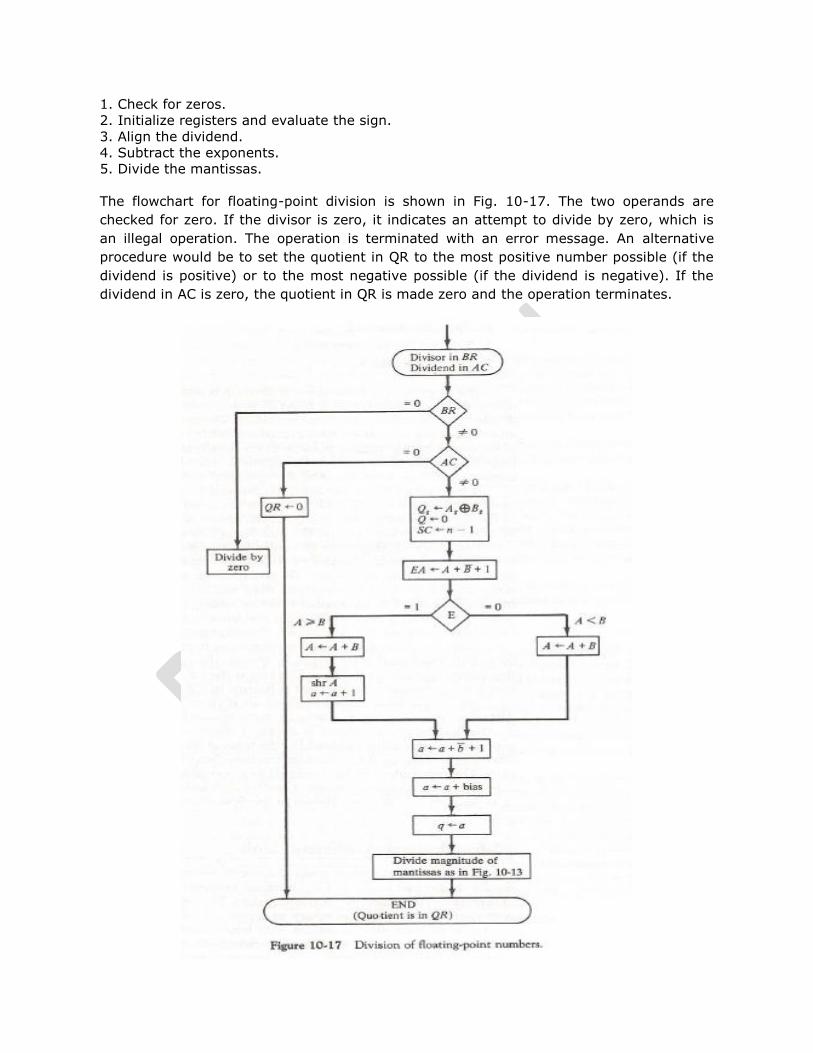
1. Check for zeros.
2. Initialize registers and evaluate the sign.
3. Align the dividend.
4. Subtract the exponents.
5. Divide the mantissas.
The flowchart for floating-point division is shown in Fig. 10-17. The two operands are
checked for zero. If the divisor is zero, it indicates an attempt to divide by zero, which is
an illegal operation. The operation is terminated with an error message. An alternative
procedure would be to set the quotient in QR to the most positive number possible (if the
dividend is positive) or to the most negative possible (if the dividend is negative). If the
dividend in AC is zero, the quotient in QR is made zero and the operation terminates.

If the operands are not zero, we proceed to determine the sign of the quotient and
store it in Q5. The sign of the dividend in As is left unchanged to be the sign of the
remainder. The Q register is cleared and the sequence counter SC is set to a number equal
to the number of bits in the quotient.
The dividend alignment is similar to the divide-overflow check in the fixed-point
operation. The proper alignment requires that the fraction dividend be smaller than the
divisor. The two fractions are compared by a subtraction test. The carry in E determines
their relative magnitude. The dividend fraction is restored to its original value by adding
the divisor. If A≥B, it is necessary to shift A once to the right and increment the dividend
exponent. Since both operands are normalized, this alignment ensures that A < B.
Next, the divisor exponent is subtracted from the dividend exponent. Since both
exponents were originally biased, the subtraction operation gives the difference without
the bias. The bias is then added and the result transferred into q because the quotient is
formed in QR. The magnitudes of the mantissas are divided as in the fixed-point case.
After the operation, the mantissa quotient resides in Q and the remainder in A. The
floating-point quotient is already normalized and resides in QR.
The exponent of the remainder should be the same as the exponent of the
dividend. The binary point for the remainder mantissa lies (n - 1) positions to the left of Al
The remainder can be converted to a normalized fraction by subtracting n - 1 from the
dividend exponent and by shift and decrement until the bit in A1 is equal to 1.
REGISTER TRANSFER AND MICRO-OPERATIONS: Register Transfer language, Register
Transfer, Bus and memory transfers, Arithmetic Micro-operations, Logic Micro-operations,
Shift Micro-operations, Arithmetic logic shift unit.
1.8 Register Transfer Language
• Digital systems are composed of modules that are constructed from digital components,
such as registers, decoders, arithmetic elements, and control logic.
• The modules are interconnected with common data and control paths to form a digital
computer system.
• The operations executed on data stored in registers are called microoperations.
• A microoperation is an elementary operation performed on the information stored
in one or more registers.
• Examples are shift, count, clear, and load.
• The internal hardware organization of a digital computer is best defined by specifying
The set of registers it contains and their functions.
The sequence of micro-operations performed on the binary information stored.
The control that initiates the sequence of micro-operations.
The symbolic notation used to describe the micro-operation transfers register
transfer among registers is called a register transfer language. The term "register transfer”
implies the availability of hardware logic circuits that can perform a stated micro-operation
and transfer the result of the operation to the same or another register.
A register transfer language is a system for expressing in symbolic form the micro-
operation sequences among the registers of a digital module. It is a convenient tool for
describing the internal organization of digital computers in concise and precise manner. It
can also be used to facilitate the design process of digital systems.
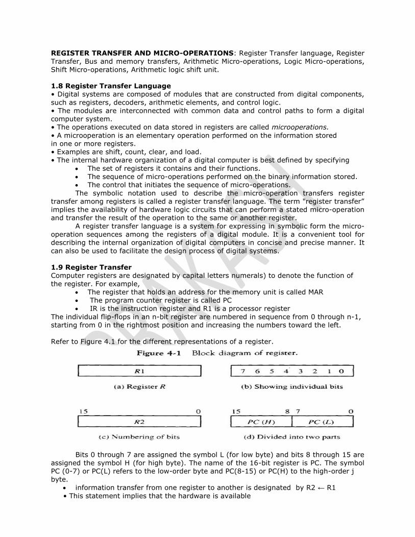
1.9 Register Transfer
Computer registers are designated by capital letters numerals) to denote the function of
the register. For example,
The register that holds an address for the memory unit is called MAR
The program counter register is called PC
IR is the instruction register and R1 is a processor register
The individual flip-flops in an n-bit register are numbered in sequence from 0 through n-1,
starting from 0 in the rightmost position and increasing the numbers toward the left.
Refer to Figure 4.1 for the different representations of a register.
Bits 0 through 7 are assigned the symbol L (for low byte) and bits 8 through 15 are
assigned the symbol H (for high byte). The name of the 16-bit register is PC. The symbol
PC (0-7) or PC(L) refers to the low-order byte and PC(8-15) or PC(H) to the high-order j
byte.
information transfer from one register to another is designated by R2 ← R1
• This statement implies that the hardware is available
o The outputs of the source must have a path to the inputs of the destination
o The destination register has a parallel load capability
• If the transfer is to occur only under a predetermined control condition, designate it
by If (P = 1) then (R2 ← R1)
or, P:R2← R1,
where P is a control function that can be either 0 or 1
• Every statement written in register transfer notation implies the presence of the
required hardware construction
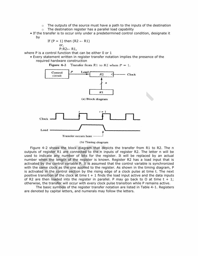
Figure 4-2 shows the block diagram that depicts the transfer from R1 to R2. The n
outputs of register R1 are connected to the n inputs of register R2. The letter n will be
used to indicate any number of bits for the register. It will be replaced by an actual
number when the length of the register is known. Register R2 has a load input that is
activated by the control variable P. It is assumed that the control variable is synchronized
with the same clock as the one applied to the register. As shown in the timing diagram, P
is activated in the control section by the rising edge of a clock pulse at time t. The next
positive transition of the clock at time t + 1 finds the load input active and the data inputs
of R2 are then loaded into the register in parallel. P may go back to O at time t + 1;
otherwise, the transfer will occur with every clock pulse transition while P remains active.
The basic symbols of the register transfer notation are listed in Table 4-1. Registers
are denoted by capital letters, and numerals may follow the letters.
1.10 Bus and memory transfers
A typical digital computer has many registers, and paths must be provided to
transfer information from one register to another. The number of wires will be excessive if
separate lines are used between each register and all other registers in the system. A
more efficient scheme for transferring information between common bus registers in a
multiple-register configuration is a common bus system. A bus structure consists of a set
of common lines, one for each bit of a register, through which binary information is
transferred one at a time. Control signals determine which register is selected by the bus
during each particular register transfer.
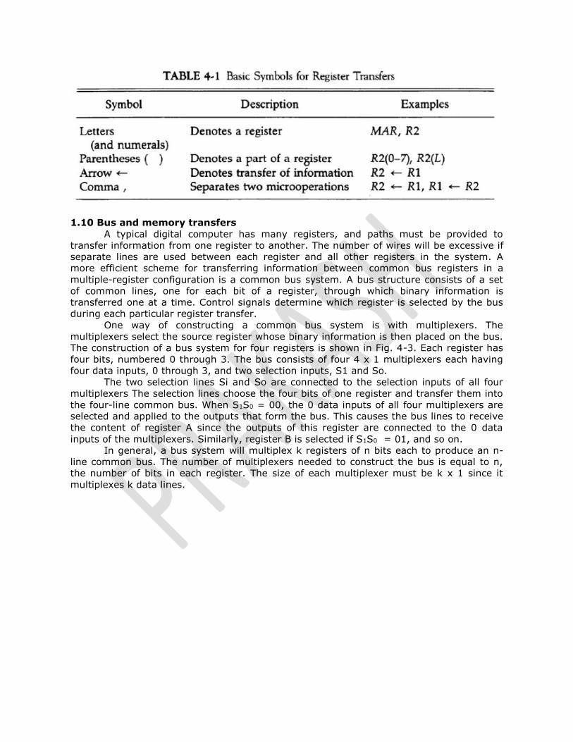
One way of constructing a common bus system is with multiplexers. The
multiplexers select the source register whose binary information is then placed on the bus.
The construction of a bus system for four registers is shown in Fig. 4-3. Each register has
four bits, numbered 0 through 3. The bus consists of four 4 x 1 multiplexers each having
four data inputs, 0 through 3, and two selection inputs, S1 and So.
The two selection lines Si and So are connected to the selection inputs of all four
multiplexers The selection lines choose the four bits of one register and transfer them into
the four-line common bus. When S1S0 = 00, the 0 data inputs of all four multiplexers are
selected and applied to the outputs that form the bus. This causes the bus lines to receive
the content of register A since the outputs of this register are connected to the 0 data
inputs of the multiplexers. Similarly, register B is selected if S1S0 = 01, and so on.
In general, a bus system will multiplex k registers of n bits each to produce an n-
line common bus. The number of multiplexers needed to construct the bus is equal to n,
the number of bits in each register. The size of each multiplexer must be k x 1 since it
multiplexes k data lines.
The transfer of information from a bus into one of many destination registers can be
accomplished by connecting the bus lines to the inputs of all destination registers and
activating the load control of the particular destination register selected.
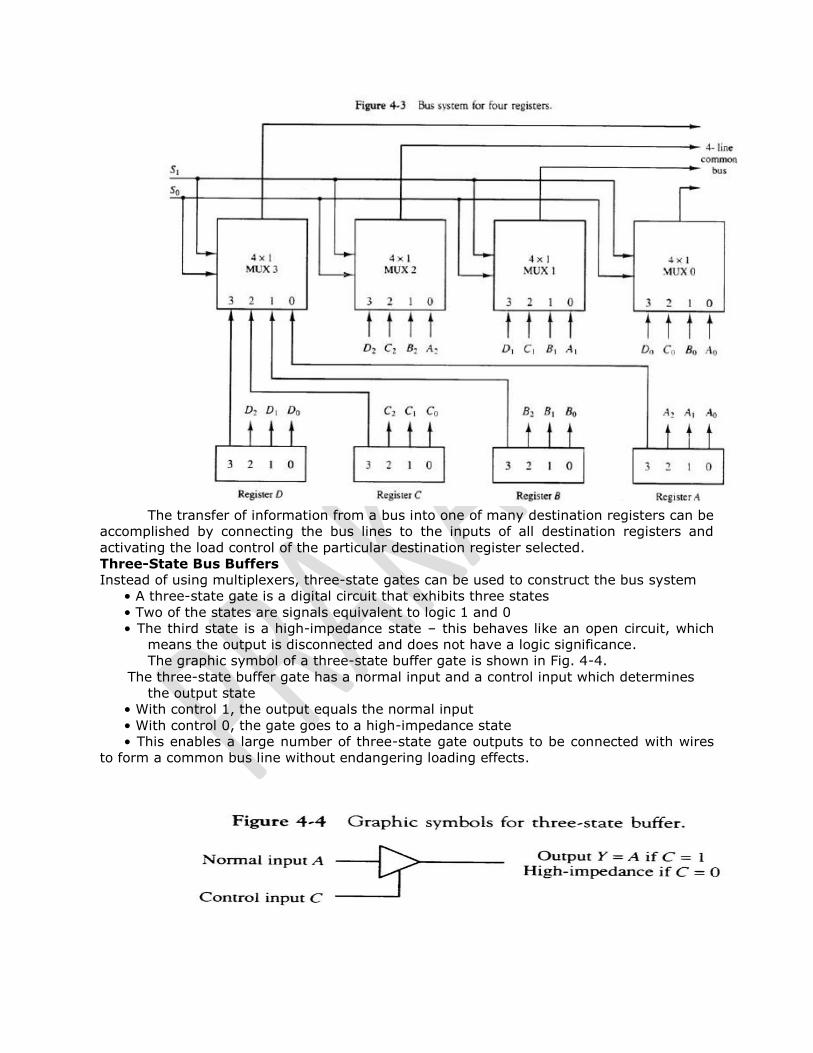
Three-State Bus Buffers
Instead of using multiplexers, three-state gates can be used to construct the bus system
• A three-state gate is a digital circuit that exhibits three states
• Two of the states are signals equivalent to logic 1 and 0
• The third state is a high-impedance state – this behaves like an open circuit, which
means the output is disconnected and does not have a logic significance.
The graphic symbol of a three-state buffer gate is shown in Fig. 4-4.
The three-state buffer gate has a normal input and a control input which determines
the output state
• With control 1, the output equals the normal input
• With control 0, the gate goes to a high-impedance state
• This enables a large number of three-state gate outputs to be connected with wires
to form a common bus line without endangering loading effects.
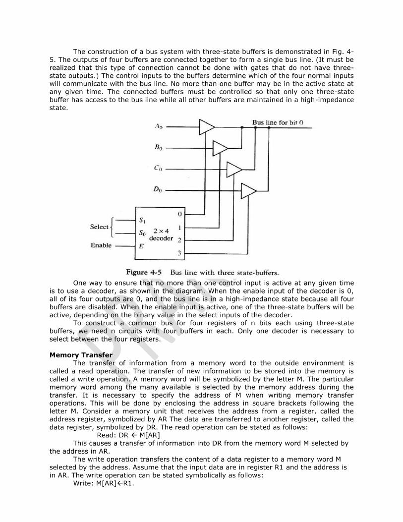
The construction of a bus system with three-state buffers is demonstrated in Fig. 4-
5. The outputs of four buffers are connected together to form a single bus line. (It must be
realized that this type of connection cannot be done with gates that do not have three-
state outputs.) The control inputs to the buffers determine which of the four normal inputs
will communicate with the bus line. No more than one buffer may be in the active state at
any given time. The connected buffers must be controlled so that only one three-state
buffer has access to the bus line while all other buffers are maintained in a high-impedance
state.
One way to ensure that no more than one control input is active at any given time
is to use a decoder, as shown in the diagram. When the enable input of the decoder is 0,
all of its four outputs are 0, and the bus line is in a high-impedance state because all four
buffers are disabled. When the enable input is active, one of the three-state buffers will be
active, depending on the binary value in the select inputs of the decoder.
To construct a common bus for four registers of n bits each using three-state
buffers, we need n circuits with four buffers in each. Only one decoder is necessary to
select between the four registers.
Memory Transfer
The transfer of information from a memory word to the outside environment is
called a read operation. The transfer of new information to be stored into the memory is
called a write operation. A memory word will be symbolized by the letter M. The particular
memory word among the many available is selected by the memory address during the
transfer. It is necessary to specify the address of M when writing memory transfer
operations. This will be done by enclosing the address in square brackets following the
letter M. Consider a memory unit that receives the address from a register, called the
address register, symbolized by AR The data are transferred to another register, called the
data register, symbolized by DR. The read operation can be stated as follows: Read: DR M[AR]
This causes a transfer of information into DR from the memory word M selected by
the address in AR.
The write operation transfers the content of a data register to a memory word M
selected by the address. Assume that the input data are in register R1 and the address is
in AR. The write operation can be stated symbolically as follows:
Write: M[AR]R1.
This causes a transfer of information from R1 into the memory word M selects by
the address in AR.
1.11Arithmetic Micro-operations:
A micro operation is an elementary operation performed with the data stored in registers.
There are four categories of the most common microoperations:
o Register transfer: transfer binary information from one register to another
o Arithmetic: perform arithmetic operations on numeric data stored in registers
o Logic: perform bit manipulation operations on non-numeric data stored in
registers
o Shift: perform shift operations on data stored in registers
• The basic arithmetic microoperations are addition, subtraction, increment,
decrement, and shift.
• Example of addition: R3 ← R1 +R2
• Subtraction is most often implemented through complementation and addition Example: R3 R1 + 𝑅2̅̅̅̅ + 1
• Adding 1 to the 1’s complement produces the 2’s complement
• Adding the contents of R1 to the 2’s complement of R2 is equivalent to subtracting.
The increment and decrement microoperations are symbolized by plus-one and minus-
one operations, respectively these microoperations are implemented with a combinational
circuit or with a binary up-down counter.
• Multiply and divide are not included as microoperations
• A microoperation is one that can be executed by one clock pulse
• Multiply (divide) is implemented by a sequence of add and shift microoperations
(subtract and shift)
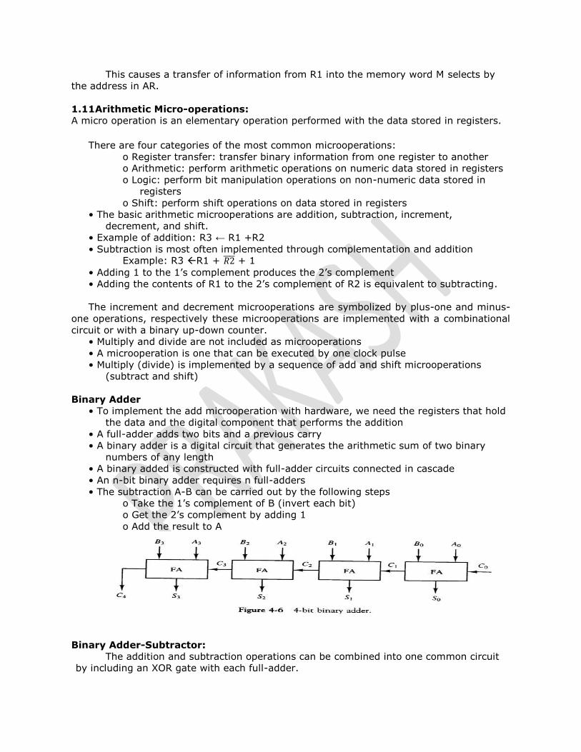
Binary Adder
• To implement the add microoperation with hardware, we need the registers that hold
the data and the digital component that performs the addition
• A full-adder adds two bits and a previous carry
• A binary adder is a digital circuit that generates the arithmetic sum of two binary
numbers of any length
• A binary added is constructed with full-adder circuits connected in cascade
• An n-bit binary adder requires n full-adders
• The subtraction A-B can be carried out by the following steps
o Take the 1’s complement of B (invert each bit)
o Get the 2’s complement by adding 1
o Add the result to A
Binary Adder-Subtractor:
The addition and subtraction operations can be combined into one common circuit
by including an XOR gate with each full-adder.
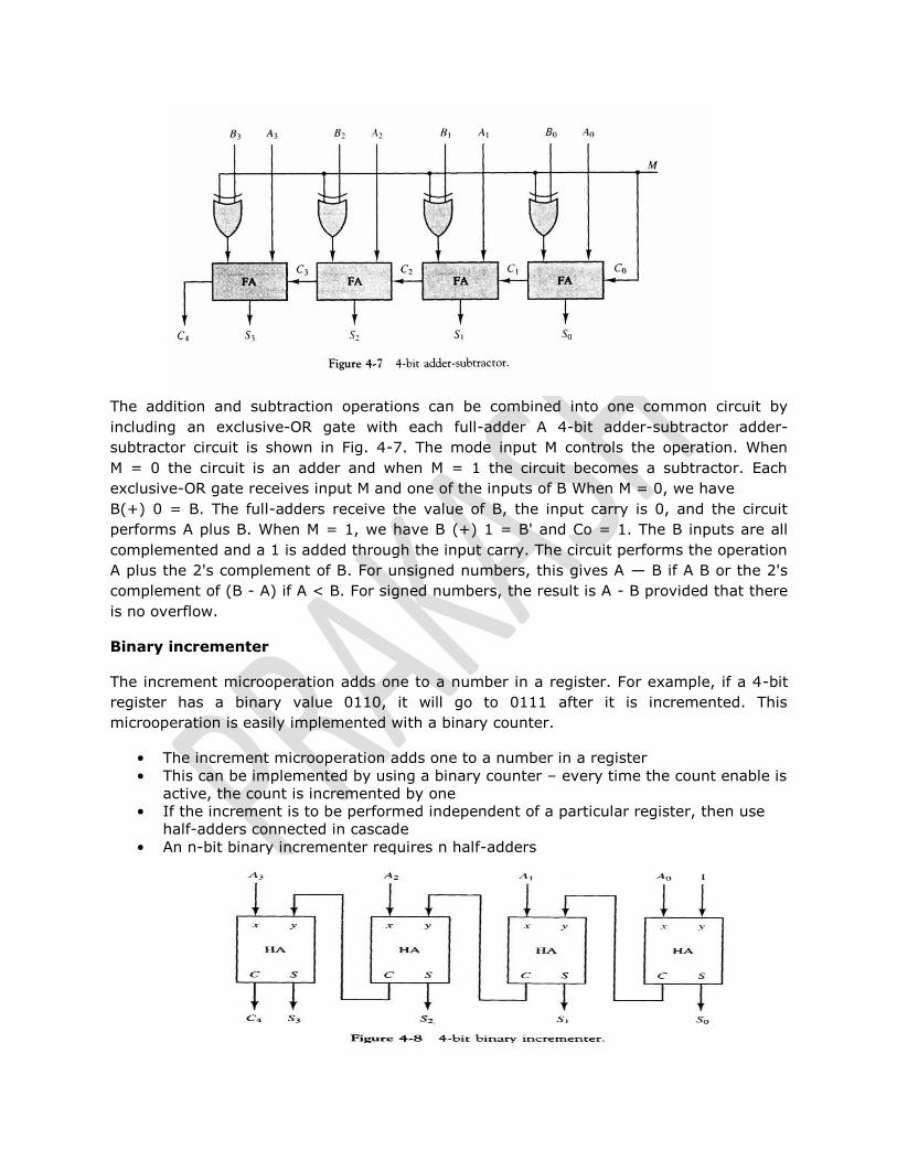
The addition and subtraction operations can be combined into one common circuit by
including an exclusive-OR gate with each full-adder A 4-bit adder-subtractor adder-
subtractor circuit is shown in Fig. 4-7. The mode input M controls the operation. When
M = 0 the circuit is an adder and when M = 1 the circuit becomes a subtractor. Each
exclusive-OR gate receives input M and one of the inputs of B When M = 0, we have
B(+) 0 = B. The full-adders receive the value of B, the input carry is 0, and the circuit
performs A plus B. When M = 1, we have B (+) 1 = B' and Co = 1. The B inputs are all
complemented and a 1 is added through the input carry. The circuit performs the operation
A plus the 2's complement of B. For unsigned numbers, this gives A — B if A B or the 2's
complement of (B - A) if A < B. For signed numbers, the result is A - B provided that there
is no overflow.
Binary incrementer
The increment microoperation adds one to a number in a register. For example, if a 4-bit
register has a binary value 0110, it will go to 0111 after it is incremented. This
microoperation is easily implemented with a binary counter.
• The increment microoperation adds one to a number in a register
• This can be implemented by using a binary counter – every time the count enable is
active, the count is incremented by one
• If the increment is to be performed independent of a particular register, then use
half-adders connected in cascade
• An n-bit binary incrementer requires n half-adders
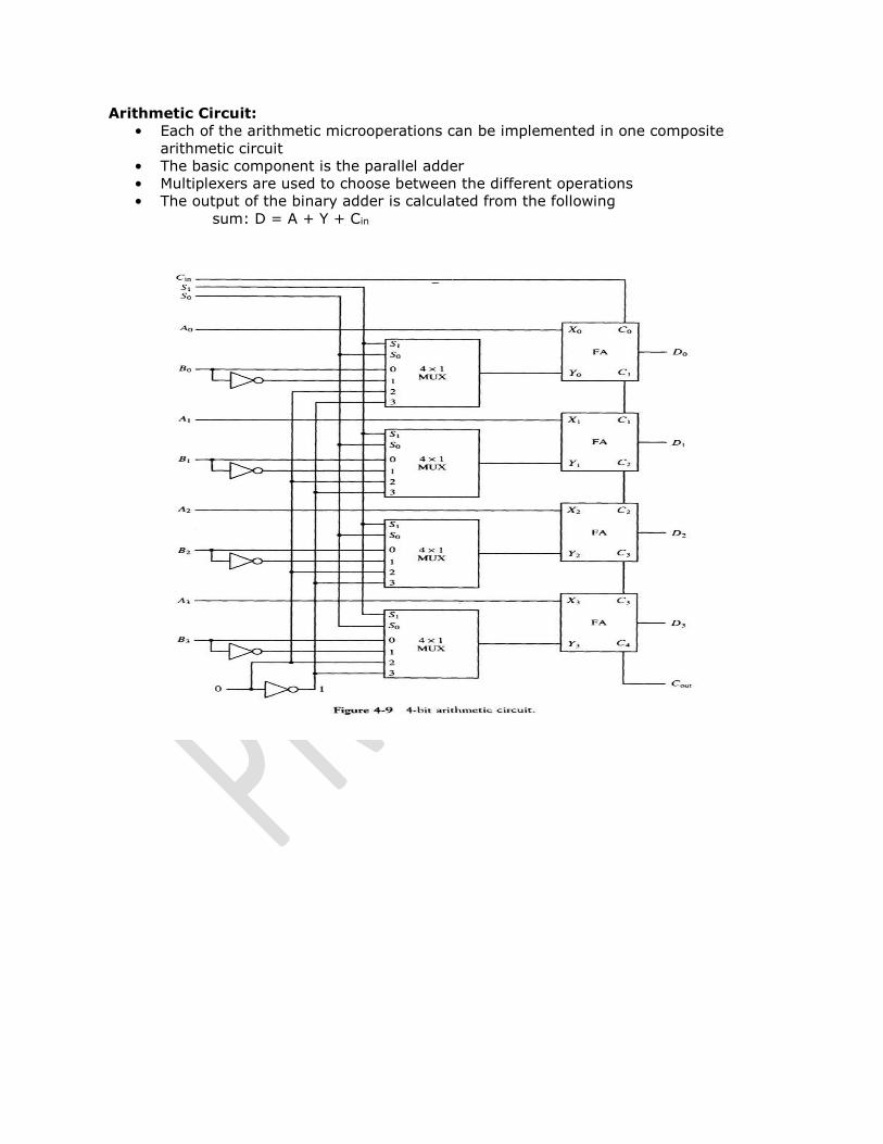
Arithmetic Circuit:
• Each of the arithmetic microoperations can be implemented in one composite
arithmetic circuit
• The basic component is the parallel adder
• Multiplexers are used to choose between the different operations
• The output of the binary adder is calculated from the following
sum: D = A + Y + Cin
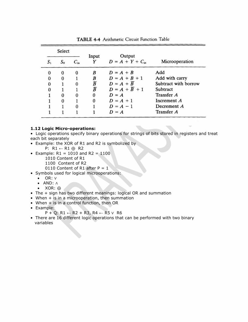
1.12 Logic Micro-operations:
• Logic operations specify binary operations for strings of bits stored in registers and treat
each bit separately
• Example: the XOR of R1 and R2 is symbolized by
P: R1 ← R1 ⊕ R2
• Example: R1 = 1010 and R2 = 1100
1010 Content of R1
1100 Content of R2
0110 Content of R1 after P = 1
• Symbols used for logical microoperations:
OR: ∨ AND: ∧ XOR: ⊕
• The + sign has two different meanings: logical OR and summation
• When + is in a microoperation, then summation
• When + is in a control function, then OR
• Example:
P + Q: R1 ← R2 + R3, R4 ← R5 ∨ R6
• There are 16 different logic operations that can be performed with two binary
variables
Truth Table:
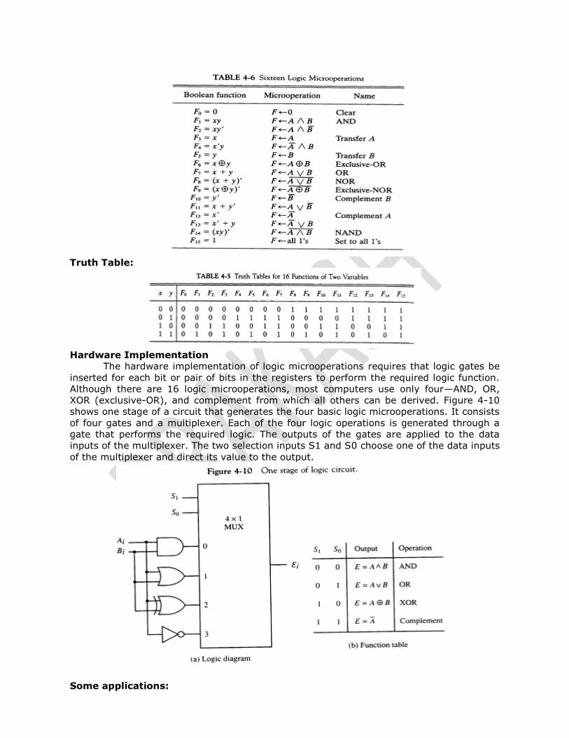
Hardware Implementation
The hardware implementation of logic microoperations requires that logic gates be
inserted for each bit or pair of bits in the registers to perform the required logic function.
Although there are 16 logic microoperations, most computers use only four—AND, OR,
XOR (exclusive-OR), and complement from which all others can be derived. Figure 4-10
shows one stage of a circuit that generates the four basic logic microoperations. It consists
of four gates and a multiplexer. Each of the four logic operations is generated through a
gate that performs the required logic. The outputs of the gates are applied to the data
inputs of the multiplexer. The two selection inputs S1 and S0 choose one of the data inputs
of the multiplexer and direct its value to the output.
Some applications:

• Logic microoperations can be used to change bit values, delete a group of bits, or insert
new bit values into a register
• The selective-set operation sets to 1 the bits in A where there are corresponding 1’s in B
1010 A before
1100 B (logic operand)
1110 A after
From the truth table we note that the bits of A after the operation are obtained from the
logic-OR operation of bits in B and previous values of A . Therefore, the OR microoperation
can be used to selectively set bits of a register.
A ← A ∨ B
• The selective-complement operation complements bits in A where there are
corresponding 1’s in B.
1010 A before
1100 B (logic operand)
0110 A after
This example again can serve as a truth table from which one can deduce that the
selective-complement operation is just an exclusive-OR microoperation. Therefore, the
exclusive-OR microoperation can be used to selectively complement bits of a register.
A ← A ⊕ B
The selective-clear operation clears to 0 the bits in A only where there are corresponding
1’s in B.
1010 A before
1100 B (logic operand)
0010 A after
Again the two leftmost bits of B are 1's, so the corresponding bits of A are cleared to 0.
One can deduce that the Boolean operation performed on the individual bits is AB' . The
corresponding logic microoperation is
A ← A ∧ B’
• The mask operation is similar to the selective-clear operation, except that the bits of A
are cleared only where there are corresponding 0’s in B.
1010 A before
1100 B (logic operand)
1000 A after
The mask operation is more convenient to use than the selective-clear operation
because most computers provide an AND instruction, and few provide an instruction that
executes the microoperation for selective-clear.
A ← A ∧ B
• The insert operation inserts a new value into a group of bits
• This is done by first masking the bits to be replaced and then ORing them with the
bits to be inserted.
0110 1010 A before
0000 1111 B (mask)
0000 1010 A after masking
And then insert the new value.
0000 1010 A before
1001 0000 B (insert)
1001 1010 A after insertion
The mask operation is an AND microoperation and the insert operation is an OR
microoperation.
• The clear operation compares the bits in A and B and produces an all 0’s result if the two
number are equal.
1010 A
1010 B
0000 A ← A ⊕ B
This operation is achieved by an exclusive-OR microoperation as shown by the following
example:
1.13 Shift Micro-operations
• Shift microoperations are used for serial transfer of data
• They are also used in conjunction with arithmetic, logic, and other data processing
operations
• There are three types of shifts: logical, circular, and arithmetic
• A logical shift is one that transfers 0 through the serial input
• The symbols shl and shr are for logical shift-left and shift-right by one position
R1 ← shl R1
• The circular shift (aka rotate) circulates the bits of the register around the two ends
without loss of information
• The symbols cil and cir are for circular shift left and right
• The arithmetic shift shifts a signed binary number to the left or right
• To the left is multiplying by 2, to the right is dividing by 2
• Arithmetic shifts must leave the sign bit unchanged
• A sign reversal occurs if the bit in Rn-1 changes in value after the shift
• This happens if the multiplication causes an overflow
• An overflow flip-flop Vs can be used to detect the overflow.
Hardware implementation:
• A bi-directional shift unit with parallel load could be used to implement this.
• Two clock pulses are necessary with this configuration: one to load the value and
another to shift.
• In a processor unit with many registers it is more efficient to implement the shift
operation with a combinational circuit .
• The content of a register to be shifted is first placed onto a common bus and the
output is connected to the combinational shifter, the shifted number is then loaded back
into the register.
• This can be constructed with multiplexers
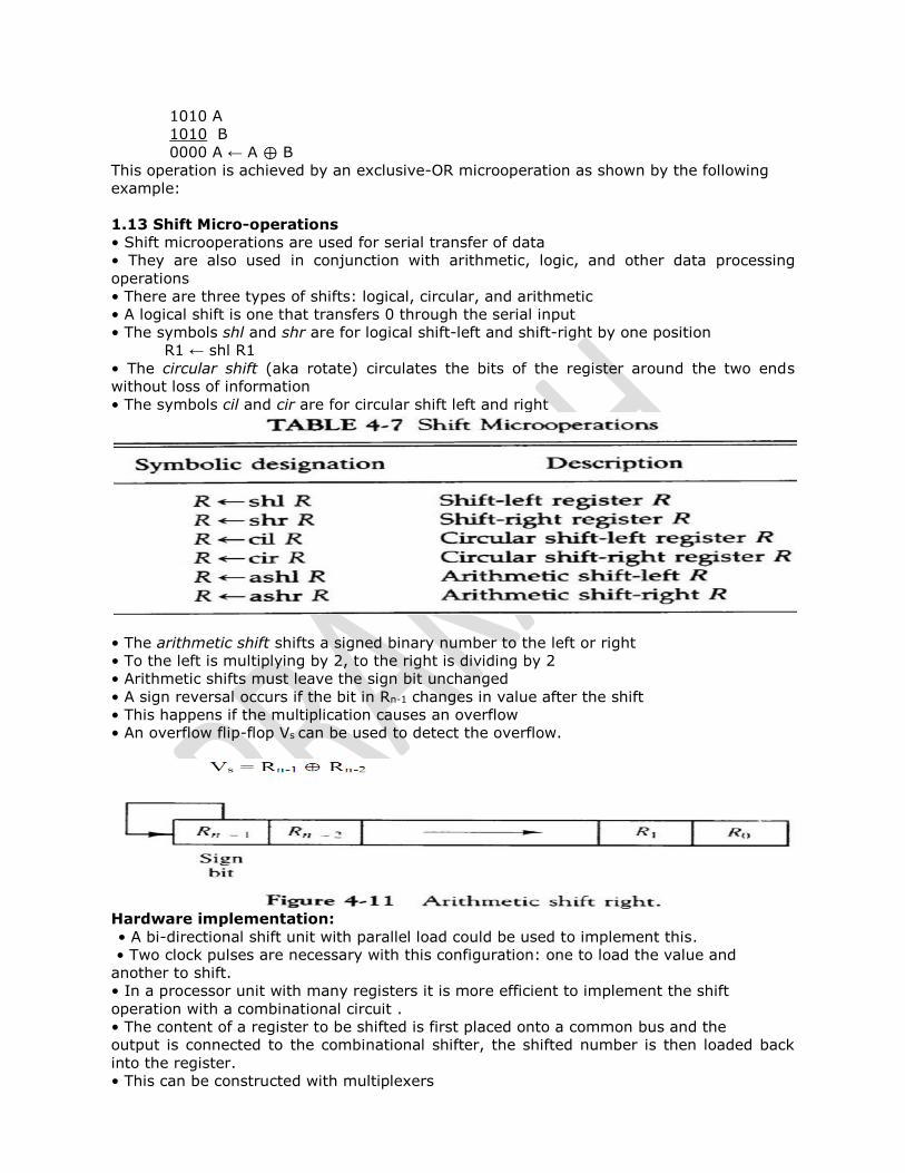
The 4-bit shifter has four data inputs, Ao through A3, and four data outputs, Ho
through H3. There are two serial inputs, one for shift left (IL) and the other for shift right
(IL). When the selection input S = 0, the input data are shifted right (down in the
diagram). When S = 1, the input data are shifted left (up in the diagram). The function
table in Fig. 4-12 shows which input goes to each output after the shift. A shifter with 11
data inputs and outputs requires 11 multiplexers. The two serial inputs can be controlled
by another multiplexer to provide the three possible types of shifts.
1.14 Arithmetic logic shift unit:
• The arithmetic logic unit (ALU) is a common operational unit connected to a number of
storage registers
• To perform a microoperation, the contents of specified registers are placed in the inputs
of the ALU
• The ALU performs an operation and the result is then transferred to a destination register
• The ALU is a combinational circuit so that the entire register transfer operation from the
source registers through the ALU and into the destination register can be performed during
one clock pulse period.
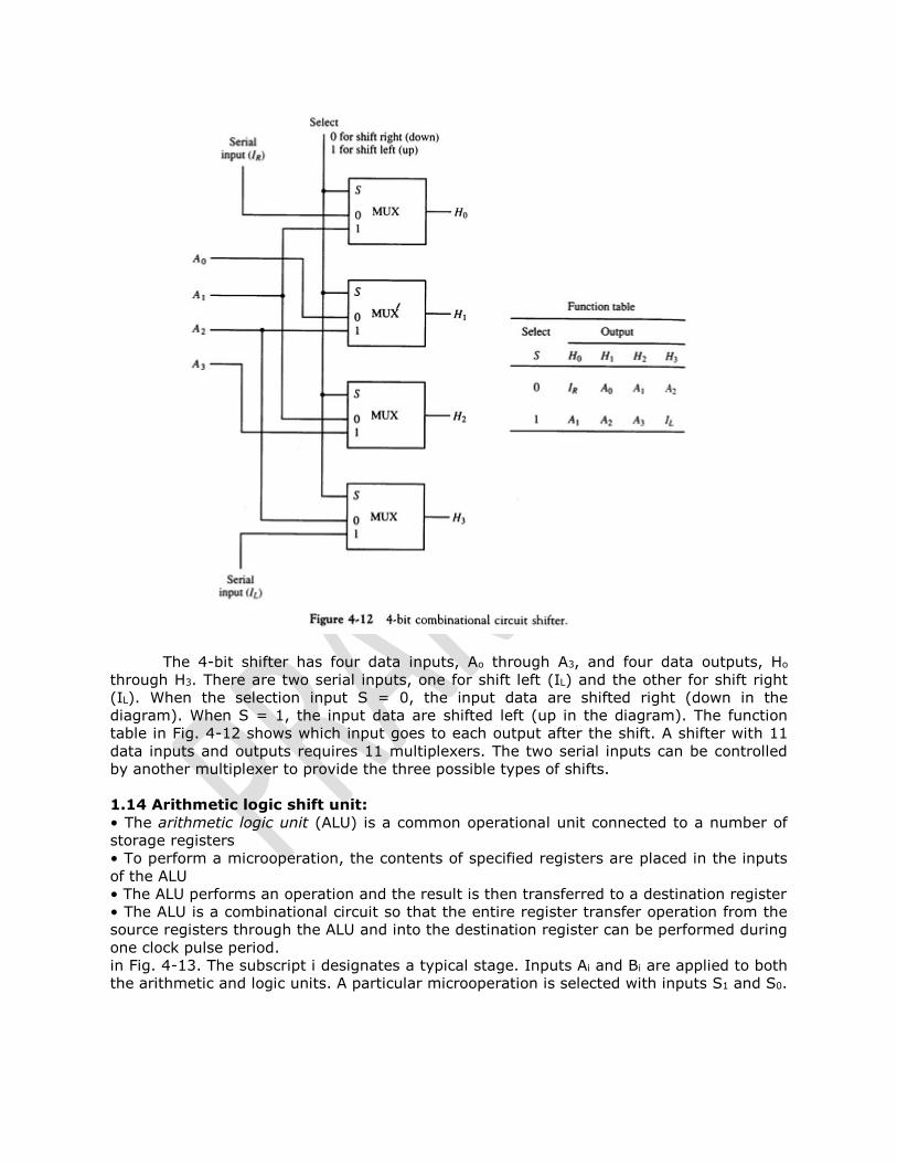
in Fig. 4-13. The subscript i designates a typical stage. Inputs Ai and Bi are applied to both
the arithmetic and logic units. A particular microoperation is selected with inputs S1 and S0.

A 4 X 1 multiplexer at the output chooses between an arithmetic output in Ei and a logic
output in Hi. The data in the multiplexer are selected with inputs S3 and S2. The other two
data inputs to the multiplexer receive inputs Ai-1 for the shift-right operation and Ai+ 1 for
the shift-left operation. Note that the diagram shows just one typical stage. The circuit of
Fig. 4-13 must be repeated n times for an n-bit ALU. The output carry Ci+1 of a given
arithmetic stage must be connected to the input carry Ci of the next stage in sequence.
The input carry to the first stage is the input carry Cin, which provides a selection variable
for the arithmetic operations.
Table 4-8 lists the 14 operations of the ALU. The first eight are arithmetic operations and
are selected with S3S2 = 00. The next four are logic operations and are selected with S3S2
= 01. The input carry has no effect during the logic operations and is marked with don’t-
care X’s. The last two operations are shift operations and are selected with S3S2= 10 and
11. The other three selection inputs have no effect on the shift.