Embed Size (px)
Citation preview

Microsystems LaboratoryUC-Berkeley, ME Dept.
1Liwei Lin, University of California at Berkeley
Micro/Nano Mechanical Systems Lab – Class#16
Liwei Lin
Professor, Dept. of Mechanical Engineering Co-Director, Berkeley Sensor and Actuator CenterThe University of California, Berkeley, CA94720
e-mail: [email protected]://www.me.berkeley.edu/~lwlin

Microsystems LaboratoryUC-Berkeley, ME Dept.
2Liwei Lin, University of California at Berkeley
Outline
The rest of the semesterNear-field Electrospinning
Microsystems LaboratoryUC-Berkeley, ME Dept.
3/8 – Other possible MEMS/NEMS labs3/13 – MD simulation lab (no lecture)3/15 – project proposal (1-2 pages ppt)3/20 – 3/22 – MD simulation lab (no lecture)4/3 – project design/progress (5 pages ppt)4/5 – review for quiz4/10 – quiz4/12 – quiz solution4/17, 4/19, 4/24, 4/26 – final presentations
Rest of the Semester

Microsystems LaboratoryUC-Berkeley, ME Dept.
4Liwei Lin, University of California at Berkeley
Outline
Electrospinning - OverviewNear-Field ElectrospinningApplicationsPVDF Nanogenrators

Microsystems LaboratoryUC-Berkeley, ME Dept.
Liwei Lin, University of California at Berkeley
ElectrospinningMechanical spinning Electrospinning – early
patent in 1934
SpinningSpinning
10―30 KV
Syringe
PolymersolutionNeedle
Collector
10―50 cm
Stretching
Whipping
Random, ContinuousNanofiber < 50nm
Microsystems LaboratoryUC-Berkeley, ME Dept.
Liwei Lin, University of California at Berkeley
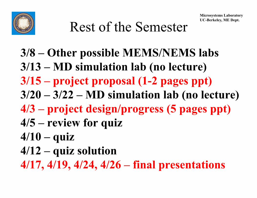
What are the Limitations? Diameter of nanofiber
Alignment
Thinner fibersThinner fibersLonger distance,
Lower concentration,Higher conductivity
Longer distance,Lower concentration,Higher conductivity Higher VoltageHigher Voltage
WhippingWhipping
D. Li et al, 2004D. Li et al, 2004 J. Kameoka et al, 2004
J. Kameoka et al, 2004A. Theron et al, 2001A. Theron et al, 2001
Microsystems LaboratoryUC-Berkeley, ME Dept.
Liwei Lin, University of California at Berkeley
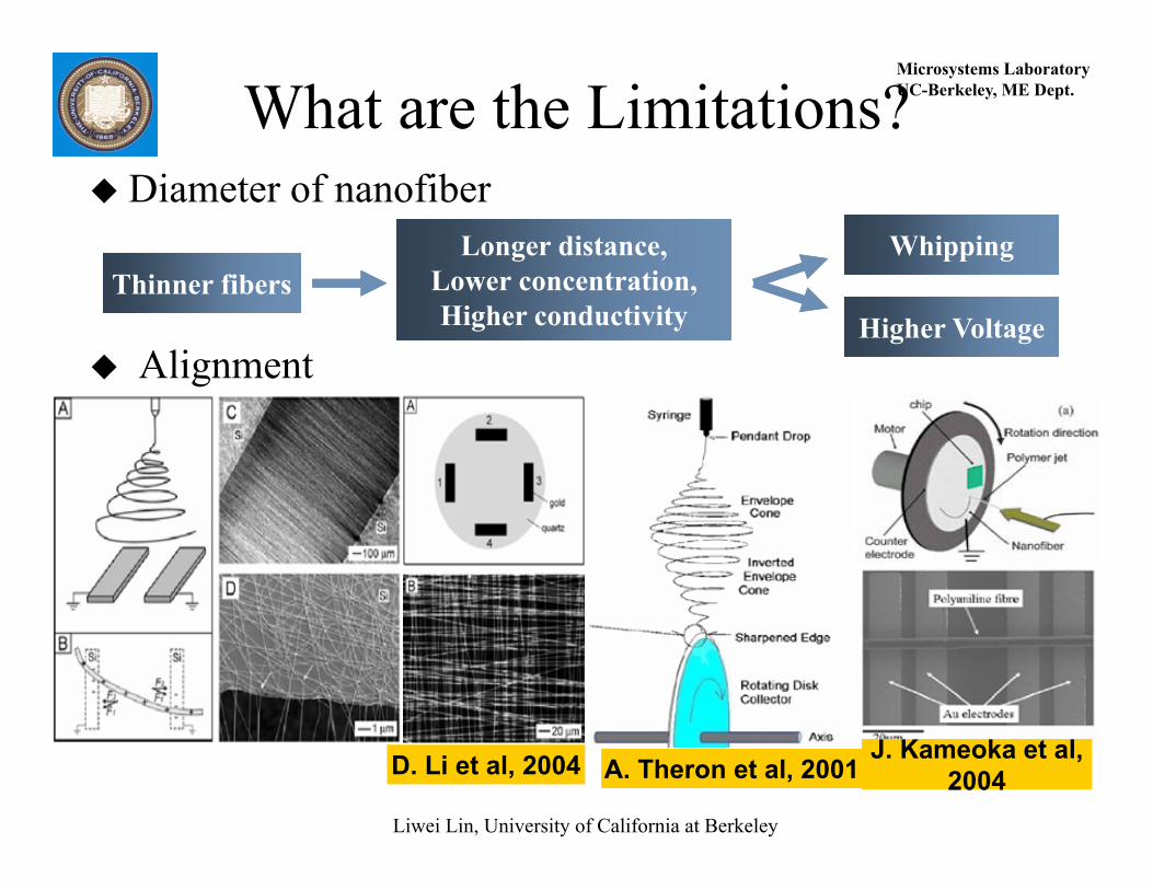
Near-Field Electrospinning Electrode-to-collector distance: 500–1000mDrive voltage: 600–1500 VTip diameter: 25 m or smaller
Collector
High Voltage
Probe Tip
Polymer Solution
Liquid Jet h
Microsystems LaboratoryUC-Berkeley, ME Dept.
Liwei Lin, University of California at Berkeley
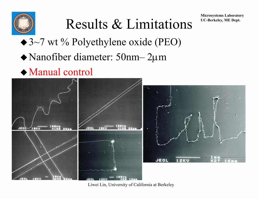
Results & Limitations 3~7 wt % Polyethylene oxide (PEO)Nanofiber diameter: 50nm– 2mManual control

Microsystems LaboratoryUC-Berkeley, ME Dept.
Liwei Lin, University of California at Berkeley
Potential Machine-controlled electrospinning

Microsystems LaboratoryUC-Berkeley, ME Dept.
Liwei Lin, University of California at Berkeley
Comparisons Conventional Electrospinning Near-Field
Needle Spinneret Metal probe tip
Several hundred µm Spinneret Diameter 25 µm or smaller
Continuous supply Polymer Supply Dip pen
10–30 KV Applied Voltage As low as 600 V
Very long Nanofiber Length Several cm
10–50 cm Electrode-to-collector Distance 500–1000 µm
Controllability
Microsystems LaboratoryUC-Berkeley, ME Dept.
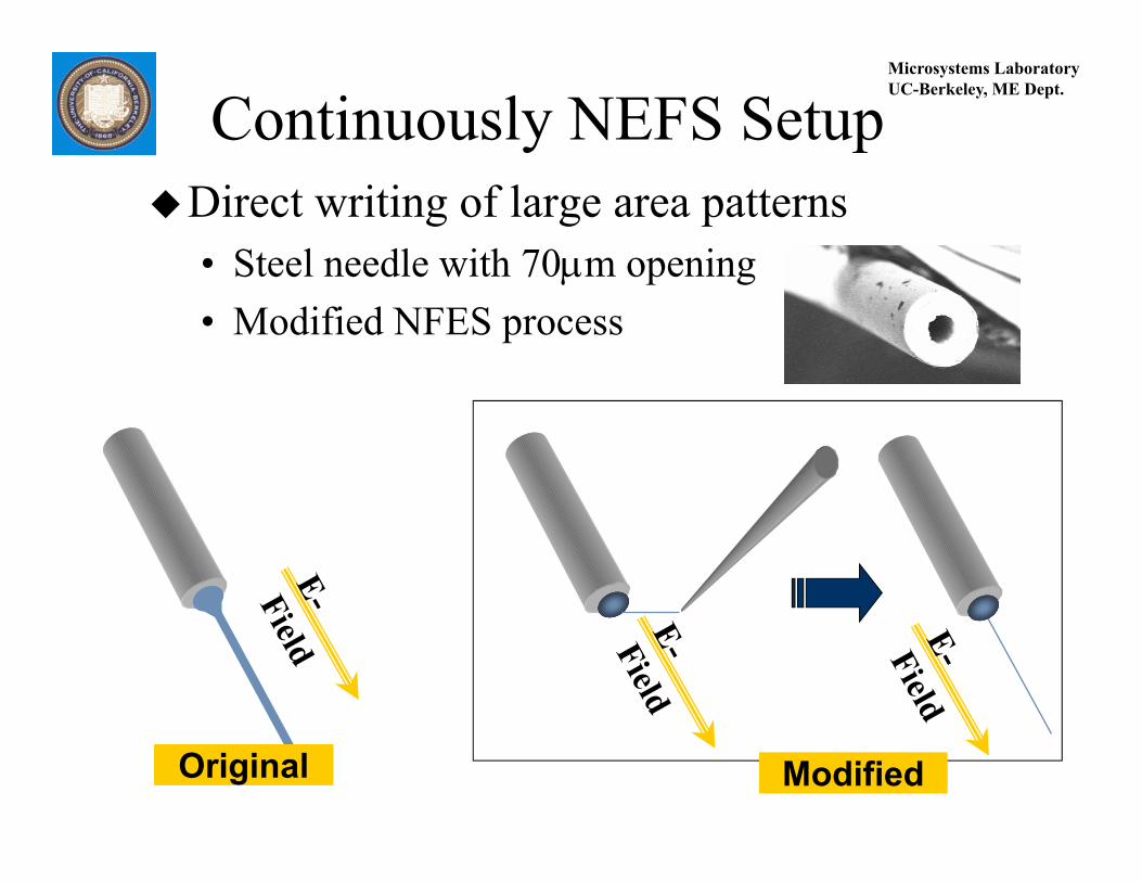
Continuously NEFS SetupDirect writing of large area patterns
• Steel needle with 70m opening• Modified NFES process
ModifiedModifiedOriginalOriginal

Microsystems LaboratoryUC-Berkeley, ME Dept.

Microsystems LaboratoryUC-Berkeley, ME Dept.
Liwei Lin, University of California at Berkeley
Continuous NEFS ResultsDirect writing of large area patterns (last week)
Microsystems LaboratoryUC-Berkeley, ME Dept.
Liwei Lin, University of California at Berkeley
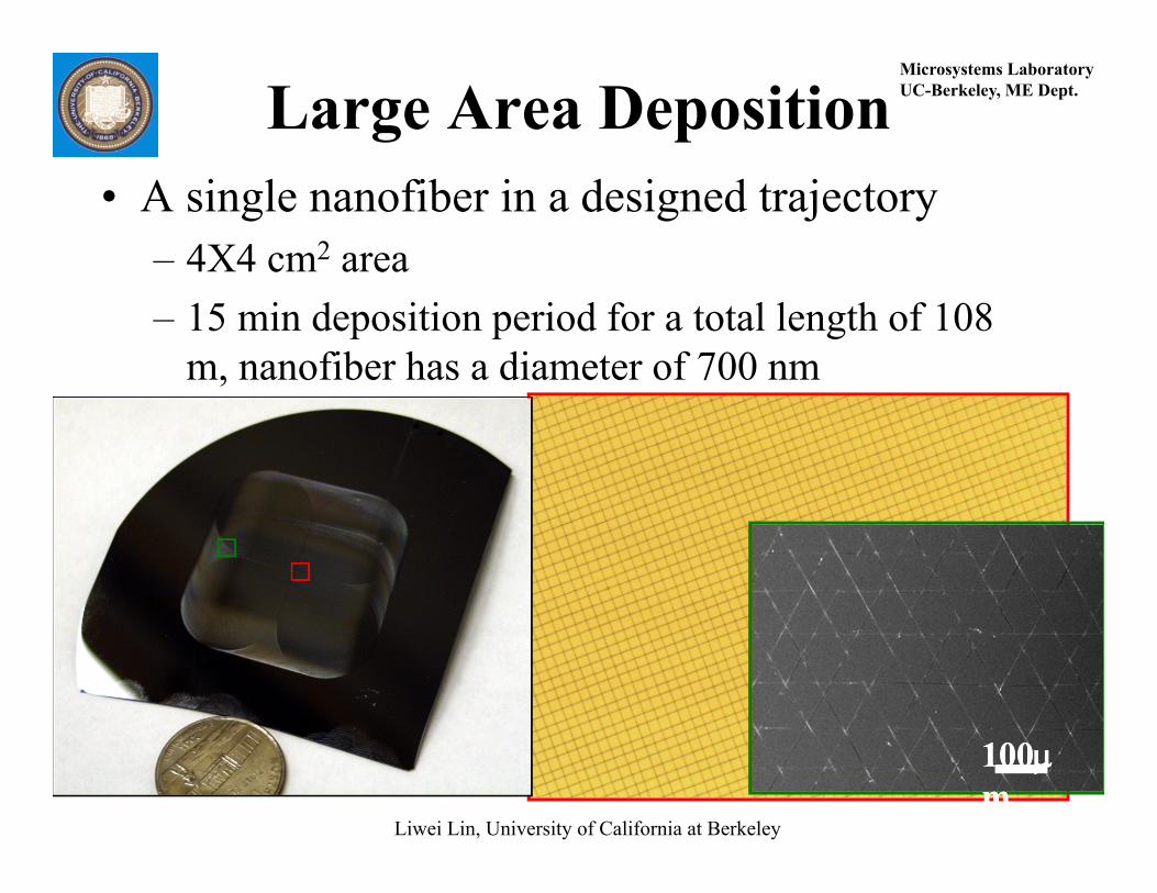
Large Area Deposition• A single nanofiber in a designed trajectory
– 4X4 cm2 area– 15 min deposition period for a total length of 108
m, nanofiber has a diameter of 700 nm
100m100m

Microsystems LaboratoryUC-Berkeley, ME Dept.
Liwei Lin, University of California at Berkeley
Application (I) - NanoSensorsDirect-write suspended nanofibers on MEMS
conductive polymer by NFES
conductive polymer by NFES
-6.00
-4.00
-2.00
0.00
2.00
4.00
6.00
-14 -12 -10 -8 -6 -4 -2 0 2 4 6 8 10 12 14
Bias [V]
Curr
ent [
μA]
100nm Nanofiber

Microsystems LaboratoryUC-Berkeley, ME Dept.
Liwei Lin, University of California at Berkeley
Application (II) - NanoAssemblyDirect-write patterning of nanoparticles
Mixing nanoparticles in nanofibers
Mixing nanoparticles in nanofibers
Removing nanofibers and growing nanowires/tubesRemoving nanofibers and growing nanowires/tubes
5 & 20nm Au nanoparticles

Microsystems LaboratoryUC-Berkeley, ME Dept.
Liwei Lin, University of California at Berkeley
Application (III) – Fluidic ConnectorDirect-write fluidic connector (analogy to wire
bonding)
3h
h
Microsystems LaboratoryUC-Berkeley, ME Dept.
Liwei Lin, University of California at Berkeley
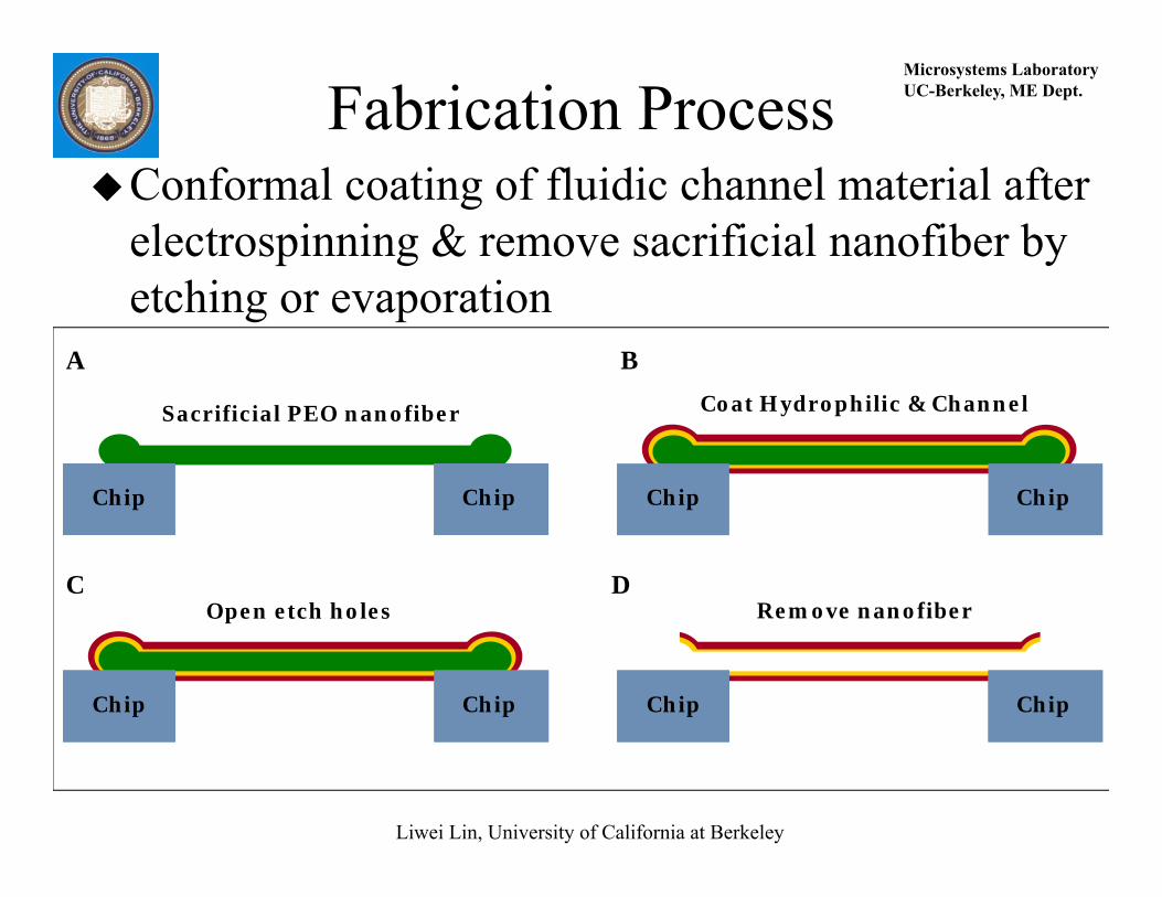
Fabrication ProcessConformal coating of fluidic channel material after
electrospinning & remove sacrificial nanofiber by etching or evaporation
A B
C D
Sacrificial PEO nanofiber
Chip ChipChip Chip
Coat Hydrophilic & Channel
Chip Chip
Open etch holes
Chip ChipChip Chip
Remove nanofiber
Chip ChipChip Chip
Microsystems LaboratoryUC-Berkeley, ME Dept.
Liwei Lin, University of California at Berkeley
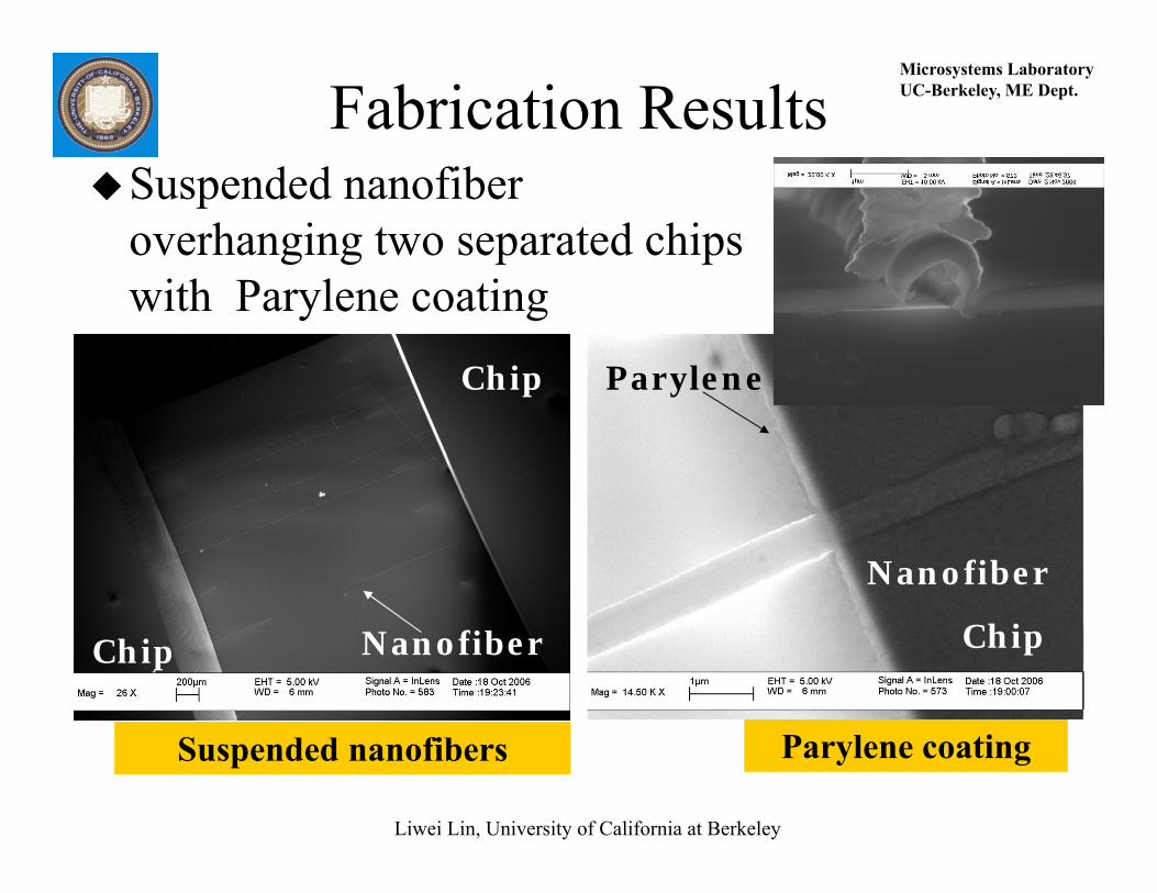
Fabrication ResultsSuspended nanofiber
overhanging two separated chips with Parylene coating
Suspended nanofibersSuspended nanofibers
Chip
Chip Nanofiber
Parylene coatingParylene coating
Chip
Nanofiber
Parylene
Microsystems LaboratoryUC-Berkeley, ME Dept.
Liwei Lin, University of California at Berkeley
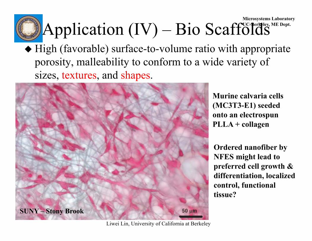
Application (IV) – Bio Scaffolds High (favorable) surface-to-volume ratio with appropriate
porosity, malleability to conform to a wide variety of sizes, textures, and shapes.
SUNY – Stony Brook
Murine calvaria cells (MC3T3-E1) seeded onto an electrospunPLLA + collagen
Ordered nanofiber by NFES might lead to preferred cell growth & differentiation, localized control, functional tissue?

Microsystems LaboratoryUC-Berkeley, ME Dept.
Liwei Lin, University of California at Berkeley
Application (V) - Composites Embedded high-modulus fibrous materials (e.g., glass
fibers, carbon fibers, carbon nanotubes) for material reinforcement
Embedding sensors & drug carriers.

Microsystems LaboratoryUC-Berkeley, ME Dept.
Liwei Lin, University of California at Berkeley
Other ApplicationsFiltration, sensing, …

©2012 University of California
Electrospun Piezoelectric Nanogenerators
Prof. Liwei Lin
Berkeley Sensor and Actuator CenterDepartment of Mechanical Engineering
University of California, Berkeley

©2012 University of California
Outline• Background
– Berkeley Sensor and Actuator Center (BSAC)– What’s electrospinning?
• Near‐Field Electrospinning (NFES)– Process design– Orderly nanofiber deposition
• Direct‐Write Piezoelectric Nanogenerator
• Conclusion

©2012 University of California
©2012 University of California

©2012 University of California
How Does It Work?• Piezoelectric Property of PVDF
– Mechanical Strain Electrical Potential– PVDF exists in several forms: , and
crystalline phases– phase is primarily responsible for
piezoelectric proper es → Dipole orientation• Poling process
– Bulk or thin film PVDF• Stretching and strong electric field
• Electrospinning→ In‐situ poling process– Electrospinning of PVDF from its solutions
promoted the formation of phase.– In contrast, only the and phases were
detected in the spin‐coated samples from the same solutions
Non‐polar phase(Before NFES)
Polar phase(After NFES)
Net dipole moment
Carbon Fluorine Hydrogenomitted
©2012 University of California

©2012 University of California
What’s the Challenge? • Conventional electrospinning
– Random orientation• The polarities of these nanofibers mostly cancel out each other and the net piezoelectric output is close to zero
• Near‐field electrospinning– Orderly nanofiber patterns with controlled direction of polarity

©2012 University of California
PVDF Nanogenerator• Fabrication process
– Spacing between electrodes: 100~500m– Fiber diameter: 500nm~3m
• Experimental setup– Inside a Faraday cage
(Not to scale)
Plastic
substr
ate
Electro
de
Plastic
substr
ate
Electro
de
A BSyringe needle
HighVoltagePolymer jet
Substrate moving direction
High Voltage
Substrate moving direction
Poling axis
(NFES direction)

©2012 University of California
Mechanism ‐ Piezoelectric Response
1. Start stretching2. Hold stretching
3. Start releasing4. End of release
V‐V+
+ ‐
RL
RL1.
2.
i
V‐V+
RL
3.
_ +
RL
4.
i
_ +
CNG
RNGqRL
V+
V‐
i
©2012 University of California
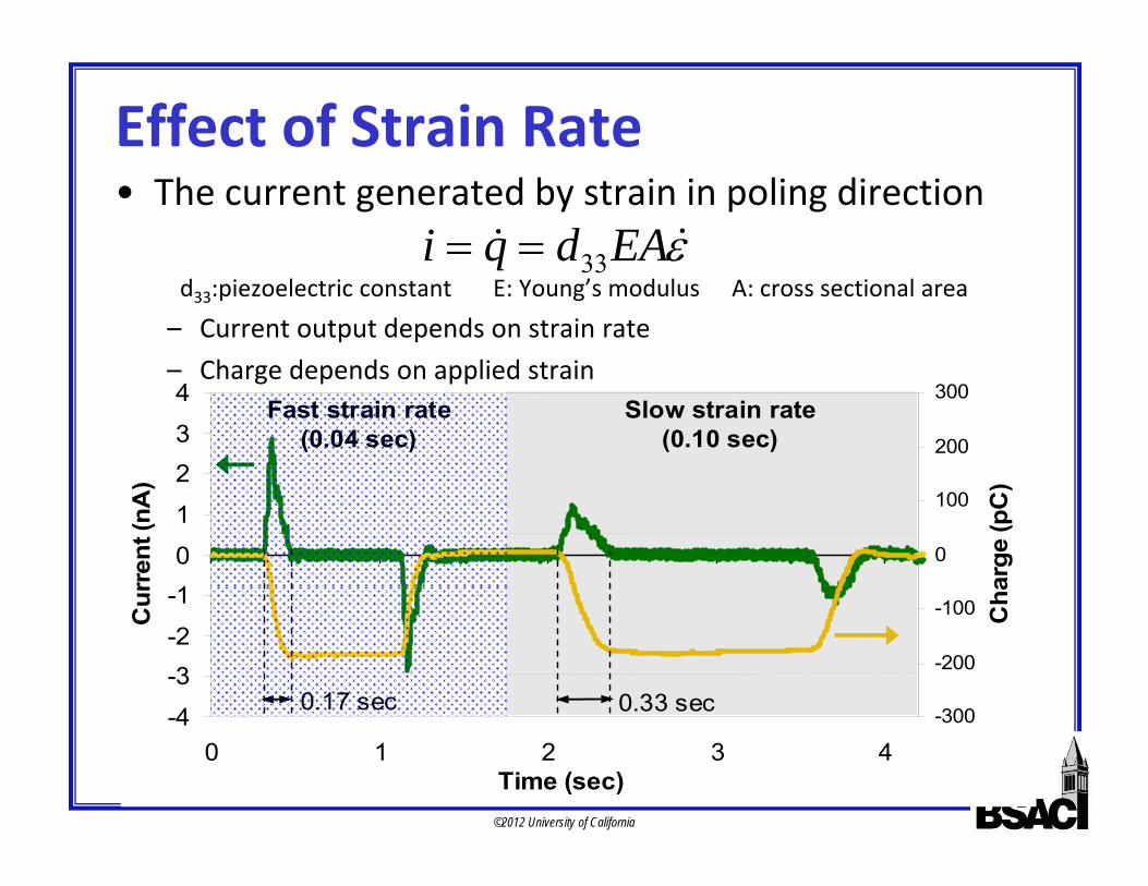
-4-3-2-101234
0 1 2 3 4Time (sec)
Cur
rent
(nA
)
-300
-200
-100
0
100
200
300
Cha
rge
(pC
)
Fast strain rate (0.04 sec)
Slow strain rate (0.10 sec)
0.17 sec 0.33 sec
Effect of Strain Rate• The current generated by strain in poling direction
d33:piezoelectric constant E: Young’s modulus A: cross sectional area
– Current output depends on strain rate– Charge depends on applied strain
33i q d EA
©2012 University of California
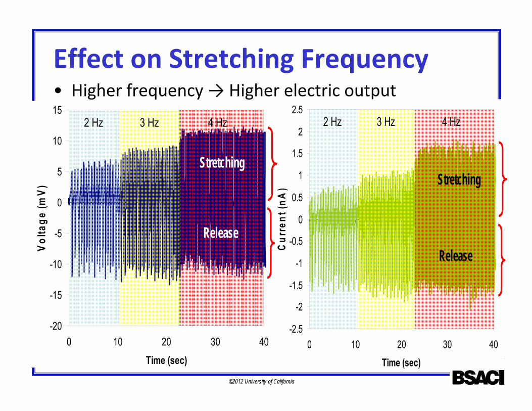
Effect on Stretching Frequency• Higher frequency → Higher electric output
-2.5
-2
-1.5
-1
-0.5
0
0.5
1
1.5
2
2.5
0 10 20 30 40Time (sec)
Cur
rent
(nA
)
2 Hz 3 Hz 4 Hz
Stretching
Release
-20
-15
-10
-5
0
5
10
15
0 10 20 30 40Time (sec)
Volta
ge (m
V)
2 Hz 3 Hz 4 Hz
Stretching
Release

©2012 University of California
Validation of Piezoelectric Response• Different materials under the same experimental setup
‐40
‐30
‐20
‐10
0
10
20
30
40
0 10 20 30 40
Voltag
e (m
V)
Time (sec)
Stretching
Release
PVDF single nanofibers
‐10
‐5
0
5
10
0 10 20 30
Voltag
e (m
V)
Time (sec)
Stretching
Release
PEO nanofiber
‐10
‐5
0
5
10
0 10 20 30
Voltag
e (m
V)
Time (sec)
Stretching
Release
PVDF random nanofibers mats

©2012 University of California
Long Term Stability Test• 0.04% strain applied at a frequency of 0.5Hz for 100 min
-6
-4
-2
0
2
4
2409 2414 2419 2424
Time (sec)
Cur
rent
(nA
)
-15
-10
-5
0
5
10
15
1421 1426 1431 1436
Time (sec)
Volta
ge (m
V)
-15
-10
-5
0
5
10
15
0 20 40 60 80 100
Time (min)
Volta
ge (m
V)
-6
-4
-2
0
2
4
0 20 40 60 80 100
Time (min)
Cur
rent
(nA
)

©2012 University of California
High Energy Conversion Efficiency?• Energy conversion efficiency
We/Wm• Total electric energy generated during stretching
We= VI dt• Total elastic energy applied during stretching
Wm= 1/8D2L0E2
0
5
10
15
20
25
0 50 100 150Film thickness (μm)
Ener
gy c
onve
rsio
n ef
ficie
ncy
(%)
0 2 4 6 8Fiber diameter (μm)
PVDF FilmPVDF fiberPVDF fiberPVDF Film
-0.5
0.0
0.5
1.0
1.5
2.0
0 0.25 0.5 0.75 1Time (sec)
Volta
ge (m
V)
-0.5
0
0.5
1
1.5
Curr
ent (
nA)
VoltageCurrent

©2012 University of California
Other Related Works in Lin Lab ‐ 1
3D Electrospinning
©2012 University of California
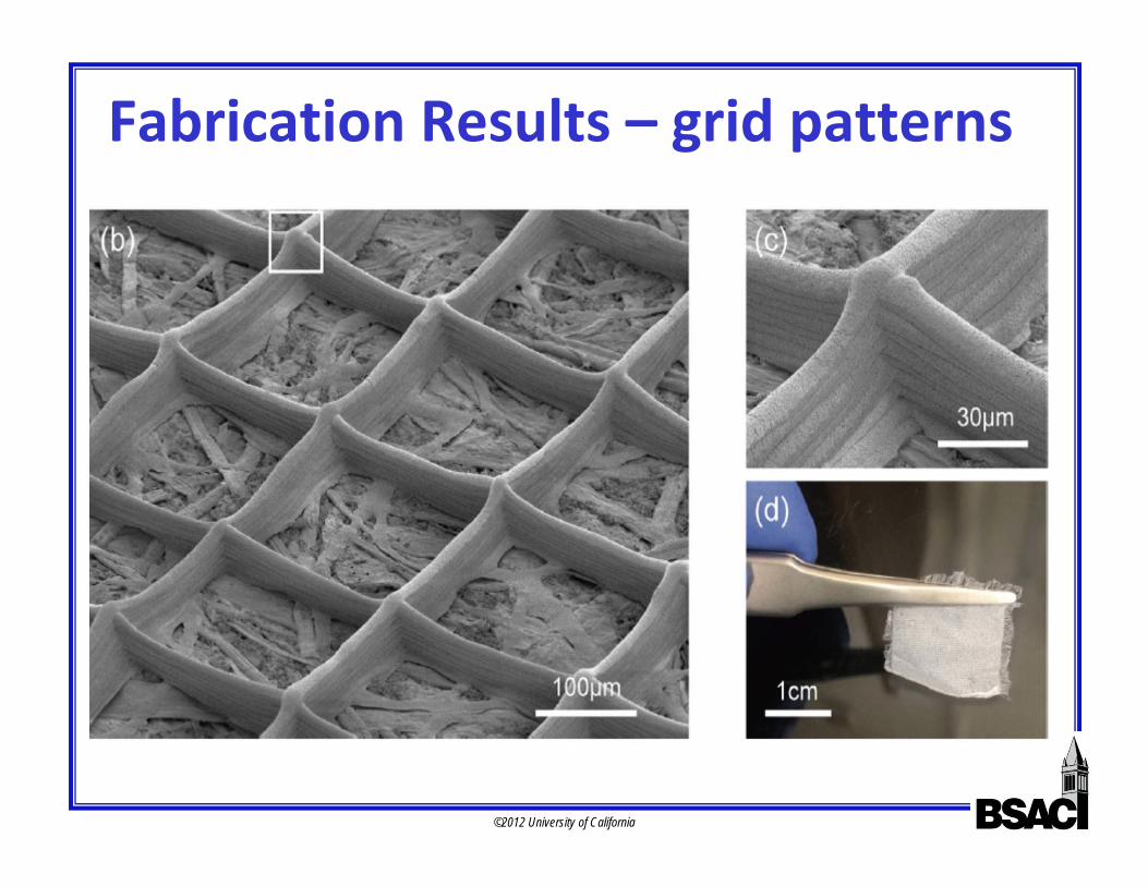
Fabrication Results – grid patterns
3D Electrospinning

©2012 University of California
Cylinder & Flower
Wall width
©2012 University of California
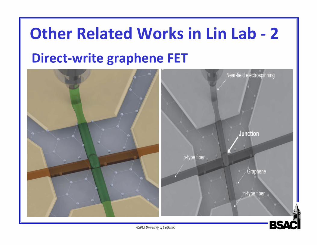
Other Related Works in Lin Lab ‐ 2Direct‐write graphene FET

©2012 University of California
Transistors, Junctions & Devicesn or p type FET & pn junction
A complimentary inverter made of p-GFET and n-GFET (npn junction in this case) is constructed