Embed Size (px)
Citation preview

Micron Engineering Clinic Fall ‘08 – Spring ‘09
Welcome to
Micron Engineering Clinic
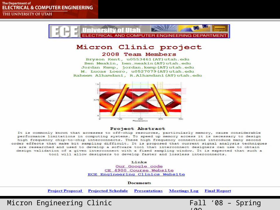
Analysis and Optimization of Multi Gb/s Chip-to-Chip Communication

Micron Engineering Clinic Fall ‘08 – Spring ‘09
Team Members
Documentation Lead Raheem Alhamdani - CE
Technical Leads
Bryson Kent - EEJordan Kemp - EELucas Loero - EE
Team LeadBen Meakin – CE

Micron Engineering Clinic Fall ‘08 – Spring ‘09
Introduction and Motivation for Modeling and Verification of Interconnects
Raheem Alhamdani
Documentation LeadComputer Engineer

Micron Engineering Clinic Fall ‘08 – Spring ‘09
Introduction
The Sponsor:
• Manufacturer of DRAM, Flash Memory, and Image Sensor Integrated Circuits
What Have They Asked Us To Do?
• Design a software application for modeling and verification of chip-to-chip interconnects

Micron Engineering Clinic Fall ‘08 – Spring ‘09
Introduction
What is Verification?
• Proving through tests and formal methods that a design does what it is intended to do
What are Chip-to-Chip Interconnects?
• Electrical systems for communication between two integrated circuits
hardwaresecrets.com

Micron Engineering Clinic Fall ‘08 – Spring ‘09
Motivation
Background
Memory and I/O Devices Operate Much Slower than CPU
Access to Off-Chip Resources is Expensive ~ 300 cycles- Usually Cycles are Wasted
Demand for Low-Power yet High-Performance- Can’t Have Wasted Cycles!
Goal: Speed Up Devices and Speed Up Interconnect

Micron Engineering Clinic Fall ‘08 – Spring ‘09
As Devices Move Towards Being Smaller, Faster, Lower PowerInterconnects Become Slower, Noisier, and Unreliable
Issues: Inter-Symbol Interference (ISI) Co-Channel Interference Timing Jitter Voltage Noise
Problem
Conventional Testing Methodologies are not Feasible or Sufficient

Micron Engineering Clinic Fall ‘08 – Spring ‘09
Eye Diagram
Voltage
Time
•What is an eye diagram?A useful tool for the qualitative analysis of signal used in digital transmission.

Micron Engineering Clinic Fall ‘08 – Spring ‘09
Eye Diagram
Time
Voltage
Voltage
Time
BitsSuperimposed
1 Unit Interval (UI)
How is it created?

Micron Engineering Clinic Fall ‘08 – Spring ‘09
Eye Diagram (Noise)
Time
Voltage
Voltage
Time
BitsSuperimposed
1 Unit Interval (UI)
Bit-stream Voltage
Noise
What Causes Noise?
• Interference from neighboring wires (Co-Channel Interference)
• Electromagnetic Interference
•Link resistance, capacitance, and inductance

Micron Engineering Clinic Fall ‘08 – Spring ‘09
Eye Diagram (Jitter)
Time
Voltage
Voltage
Time
BitsSuperimposed
1 Unit Interval (UI)
Bit-stream
Jitter
What Causes Jitter?
• Clock Variation (Skew)
• Reflection
• General Timing Uncertainty

Micron Engineering Clinic Fall ‘08 – Spring ‘09
Real Eye Diagram
Data Jitter
Clock Jitter
Signal Noise
Vref
Data Signal
Clock Signal
Vref Noise+
ReceiverSensitiv
ity
How to interpret it?

Micron Engineering Clinic Fall ‘08 – Spring ‘09
Solution
Our Objective is Not to Solve These Problems Through Better Design, but toProvide Designers with a Tool That Correctly Models and Verifies Interconnects With These Problems
Deliverables:
Cross Platform App with Graphical User Interface
Provide Worst-Case and Statistical Based Link Analysis
Spice Compatible
Correctly Model Co-Channel Interference and Tx/Rx Jitter

Micron Engineering Clinic Fall ‘08 – Spring ‘09
Project Documentation
Meeting minutes, Time-line, Progress Report , Presentations, Proposal and links are all on the team’s website: www.eng.utah.edu/~alhamdan/Micron/Micron.html
My Roles
Graphical User Interface and Software Development
GUISoftware skeletonPlotting code Code documentation
Micron Engineering Clinic Fall ‘08 – Spring ‘09
Team’s website

Micron Engineering Clinic Fall ‘08 – Spring ‘09
Meeting Minutes

Micron Engineering Clinic Fall ‘08 – Spring ‘09
Bibliography
B. K. Casper, M. Haycock, and R. Mooney, “An accurate and efficient analysis method for multi-Gb/s chip-to-chip signaling scheme”, in Digest of Technical Papers from the IEEE Symposium on VLSI Circuits, June
2002, pp. 54–57.
B. K. Casper , G. Balamurugan, J. E. Jaussi, J. Kennedy, M. Mansuri, “Future microprocessor interfaces: Analysis, design and optimization”, in Proceedings of the IEEE Custom Integrated Circuits Conference,
Sept. 2007, pp. 479-486.
P. K. Hanumolu, B. K. Casper, R. Mooney, G. Y. Wei, and U. K. Moon, “Jitter in high-speed serial and parallel links”, in Proceedings of the IEEE International Symposium on Circuits and Systems, May 2004, pp.
425–428.
Pavan Kumar Hanumolu, Bryan Casper, Randy Mooney, Gu-Yeon Wei, and Un-Ku Moon, “Analysis of PLL Clock Jitter in High-Speed Serial Links”, in IEEE Transactions on Circuits and Systems, November 2003,
pp.879-886

Micron Engineering Clinic Fall ‘08 – Spring ‘09
Questions?

Micron Engineering Clinic Fall ‘08 – Spring ‘09
Worst Case Verification of High Speed Interconnects
Bryson Kent
Technical Lead
Electrical Engineer

Micron Engineering Clinic Fall ‘08 – Spring ‘09
Introduction
•What is Worst Case analysis•Why is the Worst Case important•How to calculate the Worst Case•What are the results•Conclusion and implementation

Micron Engineering Clinic Fall ‘08 – Spring ‘09
Worst Case Analysis
•Summation of all negative effects•Good representation of what can happen if certain conditions arise•Verification of error free transmission •Classic analysis of 1 trillion bits
•(1*10^12 bits) * (10^-6sec) = over 10 days

Micron Engineering Clinic Fall ‘08 – Spring ‘09
Worst Case Eye Diagram
WC1 WC2 WC3
•Voltage Vs one period of time•Distortion sources add to close the eye•From the eye diagram we can calculate a system pass fail
Tim Hollis, Micron Senior Project Proposal
Pass/Fail

Micron Engineering Clinic Fall ‘08 – Spring ‘09
Inter-Symbol Interference
•Inter-Symbol interference is the main source of interference
•Data dependent jitter and Co-channel interference add to signal degradation
Tim Hollis, Micron Senior Project Proposal

Micron Engineering Clinic Fall ‘08 – Spring ‘09
•C(t) = transmitter symbol response•P(t) = impulse response of the channel
Worst-Case Computation
•Worst case eye diagram due to Inter-symbol interference
•Worst case eye diagram due to Inter-symbol interference and cochannel interference
J. G. Proakis, “Digital Communication”, McGraw-Hill, 3rd Ed., 1995.B. K. Casper, M. Haycock, and R. Mooney, “An accurate and efficient analysis method for multi-Gb/s chip-to-chip signaling schemes”, in Digest of Technical Papers from the IEEE Symposium on VLSI Circuits, June 2002, pp. 54–57.

Micron Engineering Clinic Fall ‘08 – Spring ‘09
891 1091 1291 1491 1691 1891 2091 2291 2491 2691 2891 30910
0.5
1
Picoseconds
Vo
ltag
eWorst Case Eye Due to Inter-symbol Interference
Data-Rate = 10 Gb/s
-100 -50 0 50 1000
0.5
1
ISIpp
= 815.9948 mV
DDJpp
= 34.3117 ps
Picoseconds
Vo
ltag
e
Pulse Response
Pre-CursorCursor
Post-Cursor
Calculating the eye diagram
891 1091 1291 1491 1691 1891 2091 2291 2491 2691 2891 30910
0.5
1
Picoseconds
Vo
ltag
eWorst Case Eye Due to Inter-symbol Interference
Data-Rate = 10 Gb/s
-100 -50 0 50 1000
0.5
1
ISIpp
= 815.9948 mV
DDJpp
= 34.3117 ps
Picoseconds
Vo
ltag
e
Pulse Response
Pre-CursorCursor
Post-Cursor
891 1091 1291 1491 1691 1891 2091 2291 2491 2691 2891 30910
0.5
1
Picoseconds
Vo
ltag
eWorst Case Eye Due to Inter-symbol Interference
Data-Rate = 10 Gb/s
-100 -50 0 50 1000
0.5
1
ISIpp
= 815.9948 mV
DDJpp
= 34.3117 ps
Picoseconds
Vo
ltag
e
Pulse Response
Pre-CursorCursor
Post-Cursor
891 1091 1291 1491 1691 1891 2091 2291 2491 2691 2891 30910
0.5
1
Picoseconds
Vo
ltag
eWorst Case Eye Due to Inter-symbol Interference
Data-Rate = 10 Gb/s
-100 -50 0 50 1000
0.5
1
ISIpp
= 815.9948 mV
DDJpp
= 34.3117 ps
Picoseconds
Vo
ltag
e
Pulse Response
Pre-CursorCursor
Post-Cursor
891 1091 1291 1491 1691 1891 2091 2291 2491 2691 2891 30910
0.5
1
Picoseconds
Vo
ltag
eWorst Case Eye Due to Inter-symbol Interference
Data-Rate = 10 Gb/s
-100 -50 0 50 1000
0.5
1
ISIpp
= 815.9948 mV
DDJpp
= 34.3117 ps
Picoseconds
Vo
ltag
e
Pulse Response
Pre-CursorCursor
Post-Cursor
891 1091 1291 1491 1691 1891 2091 2291 2491 2691 2891 30910
0.5
1
Picoseconds
Vo
ltag
eWorst Case Eye Due to Inter-symbol Interference
Data-Rate = 10 Gb/s
-100 -50 0 50 1000
0.5
1
ISIpp
= 815.9948 mV
DDJpp
= 34.3117 ps
Picoseconds
Vo
ltag
e
Pulse Response
Pre-CursorCursor
Post-Cursor
891 1091 1291 1491 1691 1891 2091 2291 2491 2691 2891 30910
0.5
1
Picoseconds
Vo
ltag
eWorst Case Eye Due to Inter-symbol Interference
Data-Rate = 10 Gb/s
-100 -50 0 50 1000
0.5
1
ISIpp
= 815.9948 mV
DDJpp
= 34.3117 ps
Picoseconds
Vo
ltag
e
Pulse Response
Pre-CursorCursor
Post-Cursor
Tim Hollis, Micron Senior Project Proposal

Micron Engineering Clinic Fall ‘08 – Spring ‘09
Results
•Calculated performance Vs given performance
-1 -0.5 0 0.5 1
x 10-10
0
0.2
0.4
0.6
0.8
1

Micron Engineering Clinic Fall ‘08 – Spring ‘09
Conclusion
•Worst case analysis is beneficial•Computation is pulse based analysis•User can define and add any distortion as desired•Results of worst case analysis match results of given test case

Micron Engineering Clinic Fall ‘08 – Spring ‘09
Questions?

Micron Engineering Clinic Fall ‘08 – Spring ‘09
Statistical Analysis ofElectrical Signaling
Jordan Kemp
Technical LeadElectrical Engineering

Micron Engineering Clinic Fall ‘08 – Spring ‘09
• Introduction
• How
• Why• What
• Summary

Micron Engineering Clinic Fall ‘08 – Spring ‘09
Introduction
• Worst Case Eye good for Pass/Fail Mask, but doesn’t give details
• Need for probability of error, rather than rigid “Pass/Fail”
Pass/Fail Mask

Micron Engineering Clinic Fall ‘08 – Spring ‘09
• Use channel impulse response, p(t), and transmitter symbol response, c(t)
Introduction
( ) ( ) ( )y t c t p t
• Find PDF (Probability Density Function) & CDF (Cumulative Distribution Function) of the channel output

Micron Engineering Clinic Fall ‘08 – Spring ‘09
Introduction
• Shows BER of transmitted data given timing uncertainty (data jitter, clock jitter) and voltage uncertainty (VREF, Rx sensitivity, ISI)
• Plot BER eye-diagram as a function of sample time, sample voltage, and probability of error

Micron Engineering Clinic Fall ‘08 – Spring ‘09
Why
• Trends Increase: Speed, Capacity Decrease: Form-Factor, Power, Cost All above decrease Signal Integrity
• Theoretically impossible to send error-free data
# errors
# transmitted bitsBit Error Rate (BER) =
( ) 0110101001101000
( ) 0110101 011010001
x t
y t
• Certain number of errors per number of bits sent specified by user/system
• Usually specified below 1
1 trillion
• Would require a 1 TRILLION bit simulation!

Micron Engineering Clinic Fall ‘08 – Spring ‘09
What
• Probabilistic data eye using channel impulse response, p(t), and transmitter symbol response, c(t) to find the PDF & CDF of the channel output
• What is a PDF? - Probability Density Function - Shows the probability that a specific value is likely to happen - Integrates to 1
• What is a CDF? - Cumulative Distribution Function - Shows the probability is less than
or equal to a specific value - Integral of the PDF

Micron Engineering Clinic Fall ‘08 – Spring ‘09
How (1)
1st Way (from *Casper paper):Recursively convolve 1UI
sample terms assuming equal probability of a
transmitted ‘0’ or ‘1’[0 -0.01] [0 0.59][0 -0.07][0 0.015][0 0.055][0 0.2][0 0.5][0 0][0 0.7](Each step scaled by ½ to account for P(0) = P(1) )
0.59
0.0
1UI
y(t)

Micron Engineering Clinic Fall ‘08 – Spring ‘09
How (1)
• VERY hardware intensive (must compute multiple convolutions)
• Must maintain certain amount of resolution, slowing computations down even more
• Very quickly run out of memory performing calculations
Problems:
[0 -0.01] [0 0.59] [0 -0.07] [0 0.015] [0 0.055] [0 0.2] [0 0.5] [0 0] . . . .
1.452 1 (no decimal resolution)1.452 1.4 (one decimal resolution)1.452 1.45 (two decimal resolution)……
delta function @ 1: [0 1 0 …] 0 1 2 . . .
delta function @ 1.4: [0 0 0 0 0 0 0 0 0 0 0 0 0 0 1 0 …] 0 .1 .2 .3 .4 .5 .6 .7 .8 .9 1 1.1 1.2 1.3 1.4 1.5 . . .

Micron Engineering Clinic Fall ‘08 – Spring ‘09
How (2)
Implemented Method (modified from previous):
[0 -0.01] + [0 0.59]+[0 -0.07]+[0 0.015]+[0 0.055]+[0 0.2]+[0 0.5]+[0 0]+[0 0.7]
• Same points taken as before, but add instead of convolve
• Keeps track of locations of delta functions
• Keeps track of heights of each delta
• Plot locations versus heights

Micron Engineering Clinic Fall ‘08 – Spring ‘09
How (2)
-.01 0
Height = 0.5
0 .59
Height = 0.5
Height = 0.25
-.01 0 .58 .59
• [0 -0.01] [0 0.59] = [0 -.01 (0+.59) (-.01+.59)] = [-.01 0 .58 .59]
• Instead of convolving, proposed method adds & concatenates

Micron Engineering Clinic Fall ‘08 – Spring ‘09
Advantages:
• VERY quick
• Easy to implement
• Infinite precision (in theory)
How (2)

Micron Engineering Clinic Fall ‘08 – Spring ‘09
Summary
• Use channel impulse response, p(t), and transmitter symbol response, c(t)
( ) ( ) ( )y t c t p t
• Shows BER of transmitted data given timing uncertainty (data jitter, clock jitter) and voltage uncertainty (VREF, Rx sensitivity, ISI)
• Find PDF (Probability Density Function) & CDF (Cumulative Distribution Function) of the channel
• Plot BER eye-diagram as a function of sample time, sample voltage, and probability of error

Micron Engineering Clinic Fall ‘08 – Spring ‘09
Questions?

Micron Engineering Clinic Fall ‘08 – Spring ‘09
MODELING JITTER IN CHIP-to-CHIP COMMUNICATION
M. Lucas Loero
Technical Lead
Electrical Engineer

Micron Engineering Clinic Fall ‘08 – Spring ‘09
PRESENTATION OBJECTIVES
• Defining Jitter
• Problems caused by Jitter
• Modeling Jitter
• Receiver Jitter
• Transmitter Jitter
• Total Jitter

Micron Engineering Clinic Fall ‘08 – Spring ‘09
DEFINING JITTER
Time
Voltage
Edge location shifted
Ideal edge location
Jitter

Micron Engineering Clinic Fall ‘08 – Spring ‘09
PROBLEMS CAUSED BY JITTER
• Power supply and environment noise causes Jitter.
• Jitter can lead to:
• Time uncertainty
• Suboptimal sampling time
• Reduce noise margin

Micron Engineering Clinic Fall ‘08 – Spring ‘09
PROBLEMS CAUSED BY JITTER

Micron Engineering Clinic Fall ‘08 – Spring ‘09
• Model the effects of Jitter in high-speed serial links
• Serial links are used for high-speed chip-to-chip
communications
MODELING JITTER

Micron Engineering Clinic Fall ‘08 – Spring ‘09
MODELING JITTER
Serial Links
Transmitter generates a train of pulses
Transmitter clock Sampler
Decision circuit

Micron Engineering Clinic Fall ‘08 – Spring ‘09
MODELING JITTER
• Traditional approach to modeling jitter
• There is two main problems with this approached
• First, simulation time
• Second, difficulty simulating serial links

Micron Engineering Clinic Fall ‘08 – Spring ‘09
Receiver Jitter
Independent and Identically Distributed
Transmitted bits
Step responseChannel impulse response
Jitter sequence
MODELING JITTER

Micron Engineering Clinic Fall ‘08 – Spring ‘09
Calculated eye diagram Simulated eye diagram
MODELING JITTER

Micron Engineering Clinic Fall ‘08 – Spring ‘09
Worst-case receiver jitter
MODELING JITTER

Micron Engineering Clinic Fall ‘08 – Spring ‘09
Worst-case ISI Worst-case receiver jitter
MODELING JITTER
Worst-case receiver eye
Time
Voltage
Voltage
Time

Micron Engineering Clinic Fall ‘08 – Spring ‘09
MODELING JITTER
Worst-case receiver eye

Micron Engineering Clinic Fall ‘08 – Spring ‘09
Transmitted bits
Step response Channel impulse response
Jitter sequence
MODELING JITTER
Transmitter Jitter

Micron Engineering Clinic Fall ‘08 – Spring ‘09
MODELING JITTER
Worst-case transmitter Jitter

Micron Engineering Clinic Fall ‘08 – Spring ‘09
Worst-case ISI Worst-case transmitter jitter
MODELING JITTER
Worst-case transmitter eye
Time
Time
VoltageVoltage

Micron Engineering Clinic Fall ‘08 – Spring ‘09
MODELING JITTER
Worst-case transmitter eye

Micron Engineering Clinic Fall ‘08 – Spring ‘09
MODELING JITTER
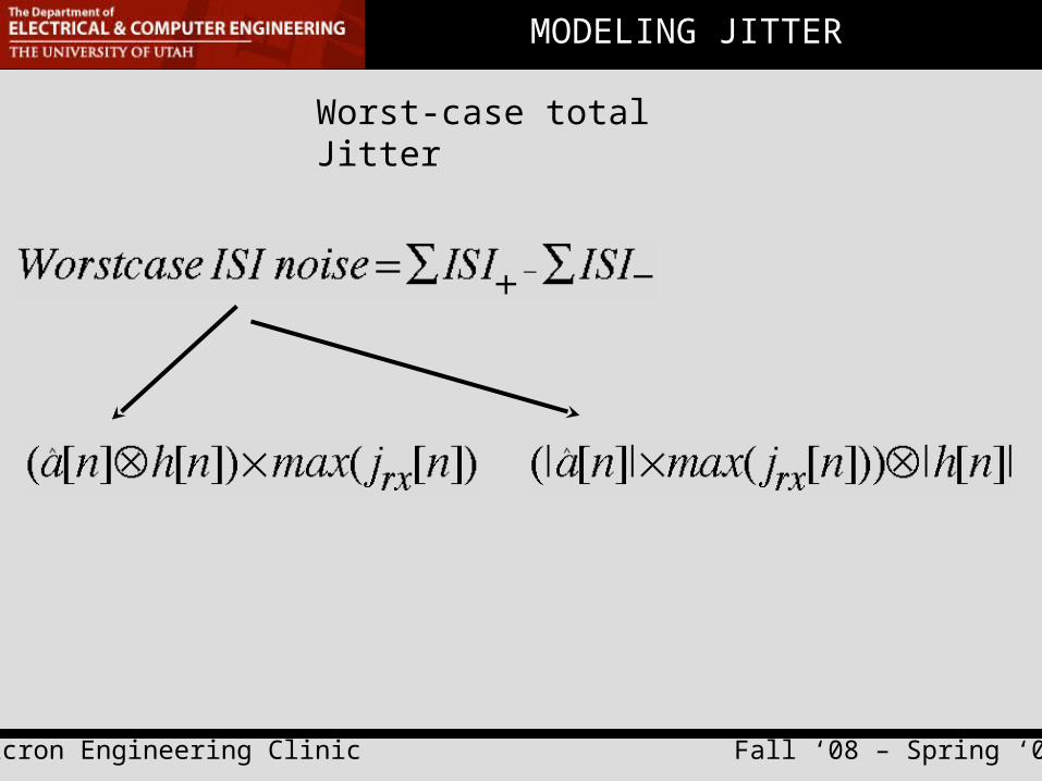
Total Jitter
Transmitter JitterReceiver Jitter
Micron Engineering Clinic Fall ‘08 – Spring ‘09
MODELING JITTER
Worst-case total Jitter

Micron Engineering Clinic Fall ‘08 – Spring ‘09
Worst-case ISI Worst-case total jitter
MODELING JITTER
Worst-case total eye
TimeTime
VoltageVoltage

Micron Engineering Clinic Fall ‘08 – Spring ‘09
MODELING JITTER
Worst-case total eye

Micron Engineering Clinic Fall ‘08 – Spring ‘09
CONCLUSION
Voltage
Time

Micron Engineering Clinic Fall ‘08 – Spring ‘09
Questions?

Micron Engineering Clinic Fall ‘08 – Spring ‘09
Project Software Engineering, Development, and Results
Ben MeakinTeam Lead
Computer [email protected]
Micron Engineering ClinicSpring '09
Micron Engineering Clinic Fall ‘08 – Spring ‘09
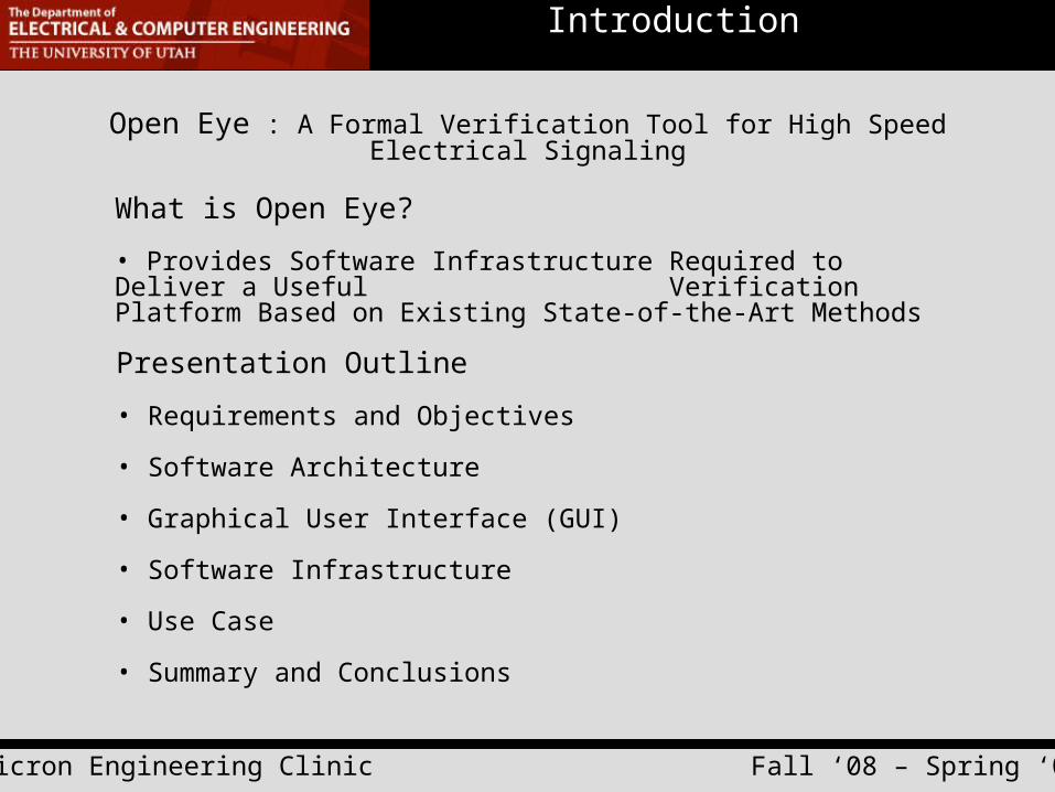
Introduction
Open Eye : A Formal Verification Tool for High Speed Electrical Signaling
What is Open Eye?
• Provides Software Infrastructure Required to Deliver a Useful Verification Platform Based on Existing State-of-the-Art Methods
Presentation Outline
• Requirements and Objectives
• Software Architecture
• Graphical User Interface (GUI)
• Software Infrastructure
• Use Case
• Summary and Conclusions

Micron Engineering Clinic Fall ‘08 – Spring ‘09
Product Requirements
Cross Platform (Windows, Linux, etc)
Graphical User Interface
No Proprietary Software License (i.e. Matlab License)
Correctly Implement Worst-Case and Statistical Link Analysis
Pass Fail Mask and Data Eye Visualization
Selectable Transmitter and Receiver Jitter
Multiple Sources of Co Channel Interference
Spice Data File Input

Micron Engineering Clinic Fall ‘08 – Spring ‘09
Product Release Status
Feature Phase Status
Worst-Case Analysis Release
Statistical Analysis Testing 25%
Static Analysis Release
Basic Plotting Release
Advanced Plotting Development 50%
Jitter Modeling Debug 75%
Co-Channel Interference Testing 75%
File Input Release
File Output Development 75%
Graphical User Interface Testing 50%
Multi-threading Testing 75%
Documentation Development 50%

Micron Engineering Clinic Fall ‘08 – Spring ‘09
Design Goals
Portability
Extensibility
Usability

View
Micron Engineering Clinic Fall ‘08 – Spring ‘09
Object Oriented Design
Model
Data IO
Signal Analysis
Parameters
Static Data
StatisticalData
Worst-CaseData
Range
MathUtility
SignalModify
Open EyeApp.
Open EyeView
OtherGUI
Classes
View
Status Q
ModelControlData Structures

Micron Engineering Clinic Fall ‘08 – Spring ‘09
Graphical User Interface Features

Micron Engineering Clinic Fall ‘08 – Spring ‘09
Graphical User Interface Features Continued

Micron Engineering Clinic Fall ‘08 – Spring ‘09
Data I/O Features
Input Data from SPICE or Any Other Column Formatted Text File
Simulation Data Objects Save State to Text FilesNo Need to Rerun To View Data
Simulation Data Output to Matlab Format Text File

Micron Engineering Clinic Fall ‘08 – Spring ‘09
Mathematical Utility Features
Discrete-Time Convolution Function
Random Number Generation over Gaussian Distribution Assortment of Vector Operations
MathUtil
+ convolution(List, List):List+ getRandom(double):double+ max(List):double+ maxAt(List):int+ min(List):double+ minAt(List):int+ indexOfClosest(List,double):int+ extendTimeScale(List):List+ getTimeUnit(List):double

Micron Engineering Clinic Fall ‘08 – Spring ‘09
Signal Analysis Features
Static Signal Analysis (Naive Method)
Data Sequence Bits Superimposed To Form Eye Diagram

Micron Engineering Clinic Fall ‘08 – Spring ‘09
Signal Analysis Features
Worst-Case Signal Analysis (Formal Method)
Mathematically Generated Worst-Case Eye Diagram
Pass/Fail Based on User Defined Sampling Window
Statistical Signal Analysis (Formal Method)
Generates a Scatter Plot of BER Diagram
Formal Methods Consider Multiple Sources of CCI and Tx/Rx Jitter
SignalAnalysis+ WCData : WorstCaseData+ StatData : StatisticalData+ EyeData : StaticData
+ doWorstCase(double,double):void+ doStatistical(double,double):void+ generateEye(double):void+ computeCCI(List,List,List,int,int):void+ passOrFail(double,double,double,double):boolean

Micron Engineering Clinic Fall ‘08 – Spring ‘09
Performance Enhancement Through Multi-Threading
Sequential Part Concurrent PartExecution Time
Convolution for Channel 0
Convolution for Channel 1
Convolution for Channel N
Convolution: Yn(t) = convolution( Pn(t), Cn(t) ), n = channel
Requires Significant Execution Time for Large Data Sets
Can Be Done Concurrently For Each Channel on Multi-Process Machines

Micron Engineering Clinic Fall ‘08 – Spring ‘09
Use Case (Worst-Case Analysis)
C(t) – Transmitter Symbol Response
P(t) – Channel Impulse Response
Data Rate: 4 Gbps
No CCI, No Jitter
Worst-Case Eye with User Defined Sampling Window

Micron Engineering Clinic Fall ‘08 – Spring ‘09
Use Case (Static Analysis)
V(t) – Data Stream{0, 1, 0, 0, 1, 1, 0, 1, 0, 1}
Data Rate: 1Gbps
Random Voltage Noise
No Jitter Added
V(t) Periods Superimposed to Get Data Eye Diagram
Micron Engineering Clinic Fall ‘08 – Spring ‘09
Summary and Conclusions
What Has Been Accomplished?
First Application to Correctly Perform Worst-Case and Statistical Link Analysis in the Public Domain
Development of a Flexible and Efficient Platform for Formal Verification of Electrical Signaling Systems
Why Does This Matter?
• Easy Verification of Aggressively Optimized Designs
• Off-Chip Memory Access Bottleneck is a Growing Problem
• Open Source Application Stimulates Academic Solutions

Micron Engineering Clinic Fall ‘08 – Spring ‘09
Questions?