Embed Size (px)
Citation preview
JLMN-Journal of Laser Micro/Nanoengineering Vol. 11, No. 1, 2016
81
Micromachining of Transparent, Semiconducting and Metallic Substrates
Using Femtosecond Laser Beams Simas Butkus*1, Aleksandr Alesenkov*1, Domas Paipulas*1, Tomas Baipulas*1, Dalia Kaškelytė*1, Martynas Barkauskas*1
and Valdas Sirutkaitis*1
*1 Vilnius University, Faculty of Physics, Department of Quantum Electronics, Laser Research Center, Saulėtekio Av. 10, Vilnius 10223,
Cutting and drilling of different materials (dielectrics, metals and semiconductors) up to 2.5 milimeters thick was carried out by laser ablation with focused femtosecond laser pulses beneath a water layer which covered the samples. The applied method demonstrated good results in term of fabrication throughput and end-quality compared to conventional fabrication in air. The improved fabrication outcomes are related to the nonlinear transformation of the femtosecond beam and en-hanced removal of ablation debris by cavitation bubble collapse. We demonstrate actual cutting speeds as high as 0.3 mm/s for transparent materials (1 mm thick), 0.15 mm/s for metals (1 mm thick), 3 mm/s for semiconducting samples (0.4 mm thick). In addition, the through-cuts have a tapper angle below 2 % and surface roughness equals approximately 5 μm.
Keywords: ablation, femtosecond, filament, water, cavitation, metals, dielectrics
1. Introduction Though laser micromachining has been under study for several decades [1], in recent times much attention has been directed towards femtosecond micromachining systems. Femtosecond laser pulses are unique for micromachining purposes due to the high intensity (>1010 W/cm2) of light that builds upon focusing. At high intensity limits, additional laser-matter interaction mechanisms are present [2], and consequently the energy of the pulse can be absorbed through non-linear absorption mechanisms [3]. In addition, beam self-actions may lead to intensity profile transformations that affect experimental outcomes (modified shape, length, quality of machined area [4]). Such laser systems have the ability to perform a substantialy higher number of micromachining tasks and are invariant to the type of the material; in addition, the active non-linear phenomena provide additional degrees of freedom (additional continuously variable parameters) when optimization or delicate tailoring procedures are required. A number of techniques exist for micromachining of various material types. Non-transparent materials are typically cut and drilled by direct ablation techniques (front-side) [5-9], spatio-temporal enhanced front-side ablation [10-12]. For transparent material fabrication, the above-mentioned techniques are applicable and additionally, modification based techniques exist: chemical etching of laser induced bulk modifications [13-18] and dicing techniques [19, 20]. Though the techniques presented are capable of performing high-quality fabrication, implementation typically requires high numerical aperture (NA) focusing conditions, precise motion translations stages and additional components leading to high equipment cost and complex operation [21]. Furthermore, gases and nanoparticles produced during fab-
rication in air, many of which are toxic, inevitably contam-inate the ambient air [22-24]. Lastly, in order to achieve greater fabrication quality, one must usually sacrifice time-efficiency or vice versa, as in the case of conventional (mechanical) machining methods [25]. In the case of material removal via ablation, even though femtosecond laser micromachining is best suited in terms of quality relative to other laser systems, imperfections (heat affected areas, cracks, edge chipping and conicity [26, 27]) are still present and are due to several reasons. Firstly, heat build-up in the impinged regions may occur during multiple pulse interactions, which leads to heat affected zones, cracking and chipping [28, 29]. Secondly, when fabricating with Gaussian pulses, the energy stored in the pulse tails is considerably less than at the center, and even though the tails do not produce strong ablation, absorption of energy still occurs which is transformed into thermal energy leading to HAZ, ripple formation or even melted regions [30]. We present an alternative front-side ablation technique by applying a water layer on top of the samples and focusing femtosecond pulses through a low NA objective. Though a similar approach has been used with longer pulse (ns) UV lasers [31, 32], our case is fundamentally different, since energy is nonlinearly absorbed and, in combination with self-focusing, the beam transforms within the water to a filament-like propagation and intensity distribution beam. If the parameters of the beam are properly chosen, an intense transformed beam can be created near the surface of the samples, which enables more efficient ablation compared to conventional focusing. In this case, filaments are formed within the water layer and are used for micromachining purposes. Experimental results with numerical simulations of filament formation, along with extensive parametric investigation, are discussed in great
DOI: 10.2961/jlmn.2016.01.0015

JLMN-Journal of Laser Micro/Nanoengineering Vol. 11, No. 1, 2016
82
detail in [33, 34]. The used approach is adventageous in various ways e.g. z axis translation is not required while several-milimeter deep structures can be fabricated, additional cooling is provided due to the added water layer which prevents temperature and tensile stress gradient formation, and large scanning rates are achievable. Moreover, the system is simple, comprised of only a few components, making it cheap and easy to use relative to other femtosecond micromachining systems. In this paper, we present cutting and drilling results for different materials fabricated with a femtosecond laser system that limits undesired thermal damage to the samples, and demonstrates great fabrication throughput even for samples as thick as ≈ 2 mm.
2. Experimental setup
The experiments were carried out using the Pharos® Yb:KGW femtosecond laser system (Light Conversion Ltd), and a two-axis galvanometric scanner (ScanLab Inc.) controlled by SCA fabrication software (Workshop of Photonics Ltd). The beam was focused with an F- theta lens (f = 100 mm) below the samples which were covered with a water layer (≈ 0.5 mm thick) so that filament formation would occur near the interface of the samples. Fig. 1 shows the experimental setup. A number of different materials were ivestigated (cut through): soda-lime glass (1 mm thick), stainless steel (0.5 – 2.5 mm thick), synthetic diamond (0.25 – 0.75 mm thick), silicon carbide (0.4 mm thick), neodymium magnet (1.9 mm thick), monocrystaline silicon (0.4 mm thick), polylactic acid (PLA) polymer (1 mm thick), copper (40 μm – 1 mm) and invar foils (40 μm thick). The water layer was formed by submerging the samples in a reservoir. The thickness of the film was measured by shining a beam from a green laser pointer onto the surface of the water film and measuring how the position of the reflected beam (from the water layer) changes on a screen when more or less water is poured into the reservoir. It was found that the thickness can be determined to an accuracy of about 50 μm. Typical writing parameters were chosen as follows: average laser power - 10 W, pulse duration - 260 fs,
repetition rate - 33.3 kHz, pulse energy - 300 μJ, wavelength - 1030 nm, focal spot diameter - 20 μm (FWHM), beam polarization - linear. Using the setup presented in Fig. 1 cutting of the priveously stated materials was carried out. For each material, a 1 cm long line along the surface of the samples was cut through, and the duration required to make the through-cut was measured. In addition, the values of the laser beam scanning speed (10 – 1500 mm/s) and the focal position (-1 – +1 mm) relative to the surface of the sample were varied for each material in order to determine the best parameter combination in terms of cutting throughput.
3. Results and discussion
The strategy for material cutting presented here is direct ablation from the top surface of the sample. Ablation in this case is induced by the laser pulses focused in water. The intense pulse (for the given experimental conditions the intensity of the pulse exceeded 2.8∙1014 W/cm2) undergoes beam transformation while propagating in non-linear media (water) in a way that increases ablation efficiency, enables thick (up to 2.5 mm) sample cutting, decreases thermal damage to the sample and redeposition of debris. The utilization of beam transformation (filamentation) in water for micromachining purposes is beneficial due to several reasons. First, as the intense beam, with power which exceeds >50 times the critical power for self-focusing, propagates in the water, it undergoes reshaping due to self-focusing and multiphoton absorption, and after a short propagation distance (< 500 μm) exhibits Gauss-Bessel beam characteristics, i.e. the intensity along the z direction stays constant for a far longer propagation length (≈ 2.5 mm), and the intensity distribution resembles a flat curve relative to what it would be with only the focusing lens and no self-actions present. Thus in such a laser mi-cromachining system when the fluence is sufficient for ablation, positioning the focal point is simple, and the use of sharp focusing objectives is unnecessary. This results in decreased sensitivity for z-axis positioning, and removes the need for translation while fabricating. These considera-tions are consistent with theoretical modelling results pre-sented in [33]. Second, the physical dimensions (possibly as low as 10 μm [35]) of the filament core are less com-pared to conventional focusing with the same lens. Third, as the sample is covered with water (substance with better thermal conductivity compared to air), better cooling of the processed samples is achieved, this results in decreased HAZ and cracks generated due to heat build-up near the cut. Fourth, due to ablation in the liquid, cavitation bubbles are formed that remove ablated particles upon collapse while fabricating and prevent debris redeposition on the sample [36]. Last, the water layer for nanosecond laser pulses aids to an increased ablation rate through a process known as laser-induced plasma confinement. The plasma that form-ing at the front surface of the glass sample is confined via the water layer, which results in better plasma-target cou-pling [37]; therefore the interaction of the plasma with the glass is prolonged, which results in more efficient ablation. Overall, these properties of the transformed beam produce greater fabrication throughput with better quality cuts and reduced sensitivity to parameter fluctuations.
Fig. 1. Experimental setup

JLMN-Journal of Laser Micro/Nanoengineering Vol. 11, No. 1, 2016
83
Using the setup presented in Fig. 1 cutting of different materials was carried out. In order to present the ad-vantages of cutting materials submerged in water, cutting experiments without the water layer were also conducted. The parameters listed in section 2 were chosen so that they would yield maximum average power (10W) and maxi-mum pulse energy (300 μJ) for this specific laser system. The thickness of the water layer was controlled by dosing the quantity of water poured into the reservoir (in the ex-periments presented here the thickness was fixed at 0.5 mm). In order to increase the rate of fabrication, parameters such as the scanning speed (linear velocity of the beam along the surface of the samples) and the position of the beam waist were varied, thus varying the position of where the intense filament forms relative to the surface of the sample. An in-depth parametric investigation will not be presented here, however scanning speed values lower than 200 mm/s are more suited for thicker (>1 mm) samples (regardles of the material) whereas higher values (≈ 500 – 600 mm/s) are more suited for lesser thickness (< 1 mm) samples. In all cases, the best focal position setting in terms of fabrication throughput is approximately 0.5 mm below the front surface of the sample.
3.1 Transparent material cutting results
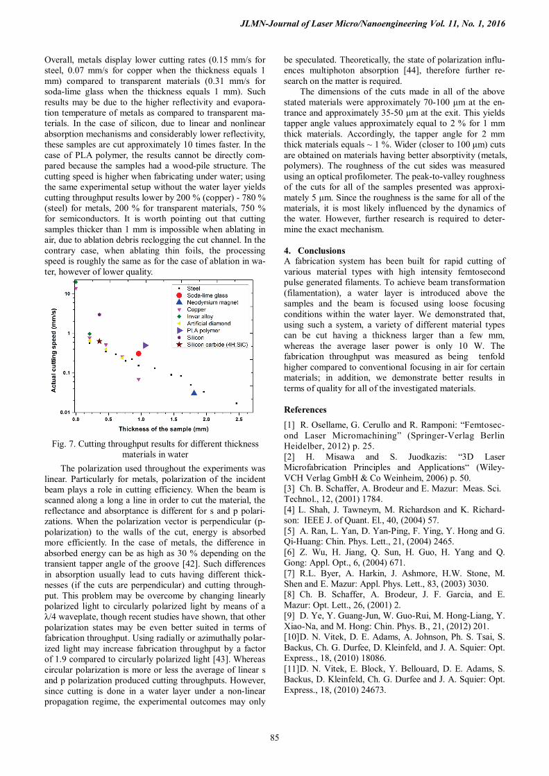
Fig. 2. Samples of cut synthetic diamond. Left - sample cut
in ambient air, right - sample cut in water. As stated, the investigated transparent materials were soda-lime glass (1 mm thick), synthetic diamond (0.25 – 0.75 mm thick) and PLA polymer (1 mm thick). In the case of transparent materials, the energy of the beam is absorbed due to multiphoton ionization and subsequent avalanche ionization mechanisms. It is worth pointing out that cutting soda-lime glass samples without the water layer is impossi-ble (given this experimental setup). When ablating glass in ambient air, the samples completely shatter due to tempera-ture induced tensile stress gradients. Glass-cutting results will not be presented here, and more rigorous studies about the matter can be found in [26, 34]. The cutting of diamonds is possible both in air and in water. Due to extremely good thermal conductivity proper-ties, these samples do not crack or shatter when exposed to intense laser radiation. However, redeposition of debris on the samples is visible when cutting in air, whereas cutting in water produces cleaner cuts as can be seen in Fig. 2. In addition, clogging of the grooves occurs by ablated dia-mond particle agglomerates, which results in decreased cutting rate and deviations from the cutting path. The cut-
ting throughput for the case of ablation in air is approxi-mately 1.8 times lower when compared to ablating in water given the same experimental conditions. Actual cutting rates will be displayed in the forthcoming sections. PLA cutting is possible both in water and in air. 1.1 mm thick PLA woodpile structures were cut. The fabrication throughput is approximately the same when cutting in air and in water. This is due to the lower band-gap of PLA, i.e. only two photon absorption is required to promote an elec-tron to the conduction band, therefore the overall absorp-tion of energy is considerably higher when compared to
other investigated materials. In addition, due to the struc-ture (woodpile) of these samples, clogging of the channels is not as prominent. Moreover, possible impurities can in-crease overall absorption through direct band gap absorp-
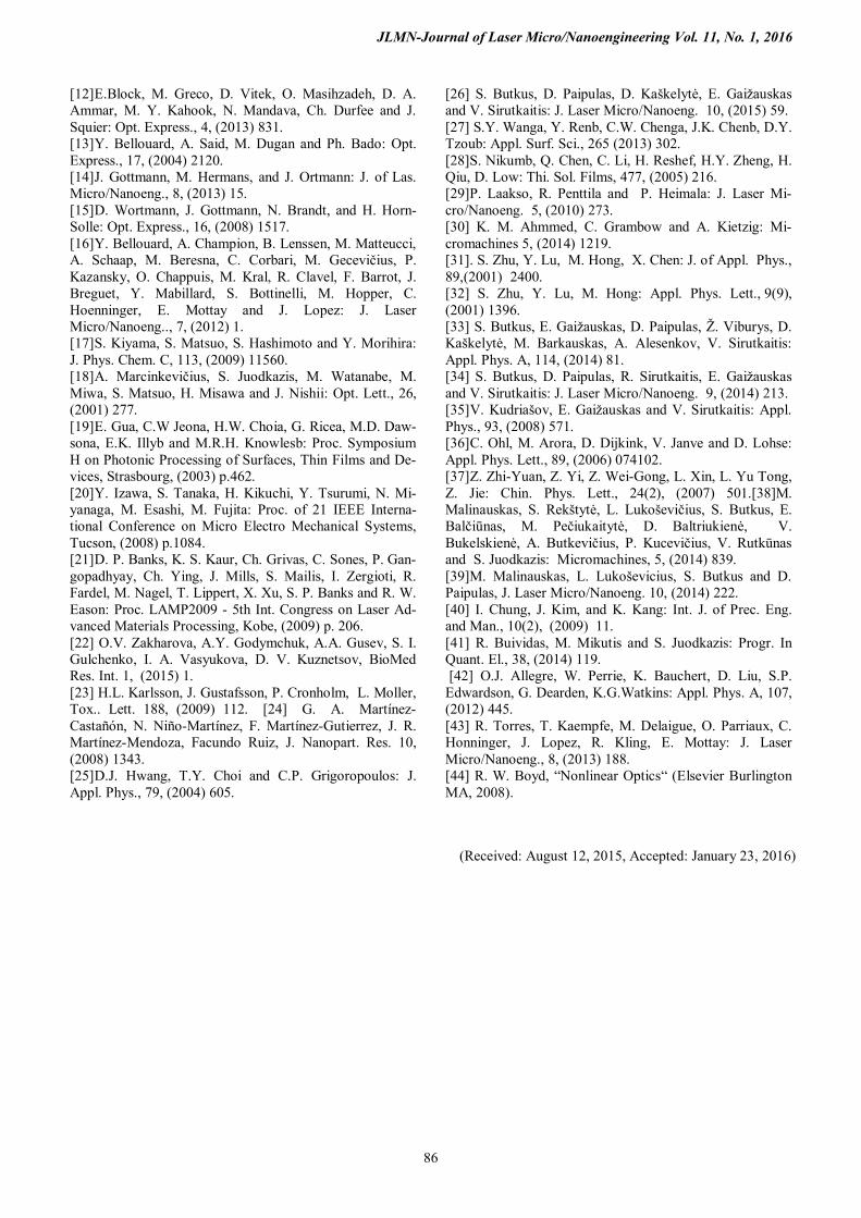
Fig 3. Sample of cut PLA. Left - sample cut in ambient air, right - sample cut in water.
Fig. 4. Steel sample (1 mm thick) cut in air (top) and in water (bottom). The actual cutting rate in water equals 0.15 mm/s whereas ablation in air takes approximately 8 times
longer.

JLMN-Journal of Laser Micro/Nanoengineering Vol. 11, No. 1, 2016
84
tion mechanisms. PLA woodpile cutting examples are dis-played in Fig. 3. One can note that when ablating in air, melting of the sides of the sample occurs, whereas samples cut in water exhibit clean cuts without any signs of melting. This is due to the additional cooling properties of the sur-rounding water. PLA woodpile cutting experiments were conducted intentionally, due to possible applications in biomedicine. PLA exhibits biodegradable properties, how-ever thermal damage (melting) initiates changes in the chemical composition of the sample that reduces these properties. Therefore, cutting in water may be considered as a unique solution for rapid manufacturing of biode-gradable components. More information on the matter can be~found~in~[38,~39].
3.2 Metal and semiconductor cutting results Cutting experiments on absorbing and conducting ma-terials (metals and semiconductors) were carried out. As in the previous section, two different strategies of micro pre-cision fabrication were employed and compared: direct laser writing by ablation in ambient air and femtosecond light filament cutting in a thin water layer. When ablating in air with low beam translation speed values (>100 mm/s), the bottom surface of the machined groove appears glossy, shining. This is due to melting and liquid dynamic process-es taking place during ablation, i.e. heat damage (HAZ) is visible even after several translations of the beam along the sample. Contrary to ablation in air, grooves produced by the same algorithm using a thin water layer are smoother, without ablation waste, also showing no signs of thermal damage. This is believed to be caused by cleansing of the ablation particles from the groove bottom from by the wa-ter shock waves as well as steam. Furthermore, in the case of filament-assisted ablation, the groove morphology as well as depth does not depend so critically on the scanning speed of the beam and energy density, as is the case of ab-lation in air. Images of through-cuts are displayed in Fig. 4. One can note that cuts done in ambient air exhibits redepo-sition of debris around the groove as well as HAZ. The grooves machined in air are wider by 8% in comparison to grooves produced under water. The fabrication throughput is approximately 8 times higher when ablating under water. The increase in fabrication throughput is believed to be due to the added cleaning properties and higher fluence values created when the beam undergoes non-linear propagation.
Using the same laser system, experiments were carried out on cutting thin copper and invar foil (40 μm thick). Cuts made in air reveal debris clusters scattered around the
cut area and HAZ (Fig. 5), whereas cuts in water reveal no such defects. An image of foil-cutting results in air and in water is presented in Fig. 5. Results are practically identical for copper and invar samples. When it comes to thin foil cutting, the ability to fabricate clean cuts without additional post-treatment is a great advantage, with potential applica-tions in shadow-mask production for OLED devices and the automobile industry [40]. Therefore cutting in water possesses unique advantages. As evident in Fig. 5, periodic surface patterns are visible near the cut area. These patterns are known as laser-induced periodic surface structures (LIPSS) or ripples, and arise due to interference between the impinging laser light and the surface electromagnetic wave (SEW), which is attributed to exitation of surface plasmon polaritons (SPPs) [41]. Consequently, these rip-ples are always perpendicular to the polarization vector. Since the ripples are present for both cases of ablation (in water and in air), we can conclude that the polarization is maintained as the pulse undergoes nonlinear propagation Optimal parameters for monocrystalline silicon cutting were also determined. The best results are achieved when the scanning speed of the beam is approximately 200 mm/s. When it comes to silicon cutting, one of the more difficult tasks is producing clean cuts without damage (thermal) to the sides of the groove. If the samples are well-polished, even small alterations to the groove sides become evident due to linear absorption mechanisms, i.e. the accumulated exposition dose of the beam’s periphery leads to damage to the sides of the sample. Such an outcome is visible in Fig. 6. The sides appear darker when the sample is cut in air; in addition, within these darker regions the monocrystalline lattice may be compromised. However, due to possible transformation of the beam, there is no evidence of damage to the sides when ablating in water.
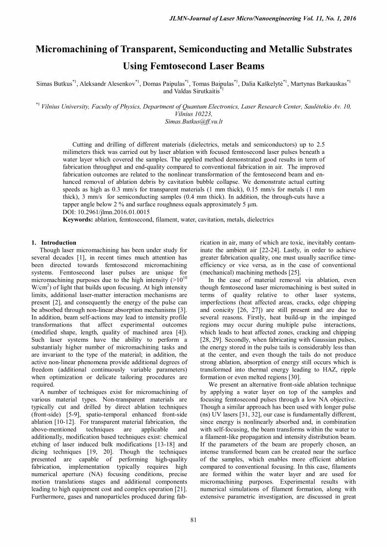
3.3 Cutting throughput comparison for different mate-rials Cutting results for different material types are dis-played in Fig. 7. The actual cutting speed was determined by cutting a 1 cm long line along the surface of the samples for each material, and the duration required to make the through-cut was measured. Afterwards, the actual cutting speed is calculated by dividing the distance by the time required to make a through-cut. All the materials were cut using optimal parameters. One can note that, given the same material type, the results roughly follow a linear de-pendence when displayed on a logarithmic (base 10) scale.
Fig. 6. Optical microscope images of cut silicon. Left - sample cut in ambient air, right - sample cut in water.
Fig. 5. Copper foil (40 μm thick cut) cutting results in air (top) and in water (bottom).
JLMN-Journal of Laser Micro/Nanoengineering Vol. 11, No. 1, 2016
85
Overall, metals display lower cutting rates (0.15 mm/s for steel, 0.07 mm/s for copper when the thickness equals 1 mm) compared to transparent materials (0.31 mm/s for soda-lime glass when the thickness equals 1 mm). Such results may be due to the higher reflectivity and evapora-tion temperature of metals as compared to transparent ma-terials. In the case of silicon, due to linear and nonlinear absorption mechanisms and considerably lower reflectivity, these samples are cut approximately 10 times faster. In the case of PLA polymer, the results cannot be directly com-pared because the samples had a wood-pile structure. The cutting speed is higher when fabricating under water; using the same experimental setup without the water layer yields cutting throughput results lower by 200 % (copper) - 780 % (steel) for metals, 200 % for transparent materials, 750 % for semiconductors. It is worth pointing out that cutting samples thicker than 1 mm is impossible when ablating in air, due to ablation debris reclogging the cut channel. In the contrary case, when ablating thin foils, the processing speed is roughly the same as for the case of ablation in wa-ter, however of lower quality.
The polarization used throughout the experiments was linear. Particularly for metals, polarization of the incident beam plays a role in cutting efficiency. When the beam is scanned along a long a line in order to cut the material, the reflectance and absorptance is different for s and p polari-zations. When the polarization vector is perpendicular (p-polarization) to the walls of the cut, energy is absorbed more efficiently. In the case of metals, the difference in absorbed energy can be as high as 30 % depending on the transient tapper angle of the groove [42]. Such differences in absorption usually lead to cuts having different thick-nesses (if the cuts are perpendicular) and cutting through-put. This problem may be overcome by changing linearly polarized light to circularly polarized light by means of a λ/4 waveplate, though recent studies have shown, that other polarization states may be even better suited in terms of fabrication throughput. Using radially or azimuthally polar-ized light may increase fabrication throughput by a factor of 1.9 compared to circularly polarized light [43]. Whereas circular polarization is more or less the average of linear s and p polarization produced cutting throughputs. However, since cutting is done in a water layer under a non-linear propagation regime, the experimental outcomes may only
be speculated. Theoretically, the state of polarization influ-ences multiphoton absorption [44], therefore further re-search on the matter is required. The dimensions of the cuts made in all of the above stated materials were approximately 70-100 μm at the en-trance and approximately 35-50 μm at the exit. This yields tapper angle values approximately equal to 2 % for 1 mm thick materials. Accordingly, the tapper angle for 2 mm thick materials equals ~ 1 %. Wider (closer to 100 μm) cuts are obtained on materials having better absorptivity (metals, polymers). The roughness of the cut sides was measured using an optical profilometer. The peak-to-valley roughness of the cuts for all of the samples presented was approxi-mately 5 μm. Since the roughness is the same for all of the materials, it is most likely influenced by the dynamics of the water. However, further research is required to deter-mine the exact mechanism.
4. Conclusions A fabrication system has been built for rapid cutting of various material types with high intensity femtosecond pulse generated filaments. To achieve beam transformation (filamentation), a water layer is introduced above the samples and the beam is focused using loose focusing conditions within the water layer. We demonstrated that, using such a system, a variety of different material types can be cut having a thickness larger than a few mm, whereas the average laser power is only 10 W. The fabrication throughput was measured as being tenfold higher compared to conventional focusing in air for certain materials; in addition, we demonstrate better results in terms of quality for all of the investigated materials. References [1] R. Osellame, G. Cerullo and R. Ramponi: “Femtosec-ond Laser Micromachining” (Springer-Verlag Berlin Heidelber, 2012) p. 25. [2] H. Misawa and S. Juodkazis: “3D Laser Microfabrication Principles and Applications“ (Wiley-VCH Verlag GmbH & Co Weinheim, 2006) p. 50. [3] Ch. B. Schaffer, A. Brodeur and E. Mazur: Meas. Sci. Technol., 12, (2001) 1784. [4] L. Shah, J. Tawneym, M. Richardson and K. Richard-son: IEEE J. of Quant. El., 40, (2004) 57. [5] A. Ran, L. Yan, D. Yan-Ping, F. Ying, Y. Hong and G. Qi-Huang: Chin. Phys. Lett., 21, (2004) 2465. [6] Z. Wu, H. Jiang, Q. Sun, H. Guo, H. Yang and Q. Gong: Appl. Opt., 6, (2004) 671. [7] R.L. Byer, A. Harkin, J. Ashmore, H.W. Stone, M. Shen and E. Mazur: Appl. Phys. Lett., 83, (2003) 3030. [8] Ch. B. Schaffer, A. Brodeur, J. F. Garcia, and E. Mazur: Opt. Lett., 26, (2001) 2. [9] D. Ye, Y. Guang-Jun, W. Guo-Rui, M. Hong-Liang, Y. Xiao-Na, and M. Hong: Chin. Phys. B., 21, (2012) 201. [10] D. N. Vitek, D. E. Adams, A. Johnson, Ph. S. Tsai, S. Backus, Ch. G. Durfee, D. Kleinfeld, and J. A. Squier: Opt. Express., 18, (2010) 18086. [11] D. N. Vitek, E. Block, Y. Bellouard, D. E. Adams, S. Backus, D. Kleinfeld, Ch. G. Durfee and J. A. Squier: Opt. Express., 18, (2010) 24673.
Fig. 7. Cutting throughput results for different thickness materials in water
JLMN-Journal of Laser Micro/Nanoengineering Vol. 11, No. 1, 2016
86
[12] E.Block, M. Greco, D. Vitek, O. Masihzadeh, D. A. Ammar, M. Y. Kahook, N. Mandava, Ch. Durfee and J. Squier: Opt. Express., 4, (2013) 831. [13] Y. Bellouard, A. Said, M. Dugan and Ph. Bado: Opt. Express., 17, (2004) 2120. [14] J. Gottmann, M. Hermans, and J. Ortmann: J. of Las. Micro/Nanoeng., 8, (2013) 15. [15] D. Wortmann, J. Gottmann, N. Brandt, and H. Horn-Solle: Opt. Express., 16, (2008) 1517. [16] Y. Bellouard, A. Champion, B. Lenssen, M. Matteucci, A. Schaap, M. Beresna, C. Corbari, M. Gecevičius, P. Kazansky, O. Chappuis, M. Kral, R. Clavel, F. Barrot, J. Breguet, Y. Mabillard, S. Bottinelli, M. Hopper, C. Hoenninger, E. Mottay and J. Lopez: J. Laser Micro/Nanoeng.., 7, (2012) 1. [17] S. Kiyama, S. Matsuo, S. Hashimoto and Y. Morihira: J. Phys. Chem. C, 113, (2009) 11560. [18] A. Marcinkevičius, S. Juodkazis, M. Watanabe, M. Miwa, S. Matsuo, H. Misawa and J. Nishii: Opt. Lett., 26, (2001) 277. [19] E. Gua, C.W Jeona, H.W. Choia, G. Ricea, M.D. Daw-sona, E.K. Illyb and M.R.H. Knowlesb: Proc. Symposium H on Photonic Processing of Surfaces, Thin Films and De-vices, Strasbourg, (2003) p.462. [20] Y. Izawa, S. Tanaka, H. Kikuchi, Y. Tsurumi, N. Mi-yanaga, M. Esashi, M. Fujita: Proc. of 21 IEEE Interna-tional Conference on Micro Electro Mechanical Systems, Tucson, (2008) p.1084. [21] D. P. Banks, K. S. Kaur, Ch. Grivas, C. Sones, P. Gan-gopadhyay, Ch. Ying, J. Mills, S. Mailis, I. Zergioti, R. Fardel, M. Nagel, T. Lippert, X. Xu, S. P. Banks and R. W. Eason: Proc. LAMP2009 - 5th Int. Congress on Laser Ad-vanced Materials Processing, Kobe, (2009) p. 206. [22] O.V. Zakharova, A.Y. Godymchuk, A.A. Gusev, S. I. Gulchenko, I. A. Vasyukova, D. V. Kuznetsov, BioMed Res. Int. 1, (2015) 1. [23] H.L. Karlsson, J. Gustafsson, P. Cronholm, L. Moller, Tox..~Lett.~188,~(2009)~112. [24] G. A. Martínez-Castañón, N. Niño-Martínez, F. Martínez-Gutierrez, J. R. Martínez-Mendoza, Facundo Ruiz, J. Nanopart. Res. 10, (2008) 1343. [25] D.J. Hwang, T.Y. Choi and C.P. Grigoropoulos: J. Appl. Phys., 79, (2004) 605.
[26] S. Butkus, D. Paipulas, D. Kaškelytė, E. Gaižauskas and V. Sirutkaitis: J. Laser Micro/Nanoeng. 10, (2015) 59. [27] S.Y. Wanga, Y. Renb, C.W. Chenga, J.K. Chenb, D.Y. Tzoub: Appl. Surf. Sci., 265 (2013) 302. [28]S. Nikumb, Q. Chen, C. Li, H. Reshef, H.Y. Zheng, H. Qiu, D. Low: Thi. Sol. Films, 477, (2005) 216. [29]P. Laakso, R. Penttila and P. Heimala: J. Laser Mi-cro/Nanoeng. 5, (2010) 273. [30] K. M. Ahmmed, C. Grambow and A. Kietzig: Mi-cromachines 5, (2014) 1219. [31]. S. Zhu, Y. Lu, M. Hong, X. Chen: J. of Appl. Phys., 89,(2001)~2400. [32] S. Zhu, Y. Lu, M. Hong: Appl. Phys. Lett., 9(9), (2001) 1396. [33] S. Butkus, E. Gaižauskas, D. Paipulas, Ž. Viburys, D. Kaškelytė, M. Barkauskas, A. Alesenkov, V. Sirutkaitis: Appl. Phys. A, 114, (2014) 81. [34] S. Butkus, D. Paipulas, R. Sirutkaitis, E. Gaižauskas and V. Sirutkaitis: J. Laser Micro/Nanoeng. 9, (2014) 213. [35] V. Kudriašov, E. Gaižauskas and V. Sirutkaitis: Appl. Phys., 93, (2008) 571. [36] C. Ohl, M. Arora, D. Dijkink, V. Janve and D. Lohse: Appl. Phys. Lett., 89, (2006) 074102. [37] Z. Zhi-Yuan, Z. Yi, Z. Wei-Gong, L. Xin, L. Yu Tong, Z. Jie: Chin. Phys. Lett., 24(2), (2007) 501.[38]M. Malinauskas, S. Rekštytė, L. Lukoševičius, S. Butkus, E. Balčiūnas, M. Pečiukaitytė, D. Baltriukienė, V. Bukelskienė, A. Butkevičius, P. Kucevičius, V. Rutkūnas and S. Juodkazis: Micromachines, 5, (2014) 839. [39]M. Malinauskas, L. Lukoševicius, S. Butkus and D. Paipulas, J. Laser Micro/Nanoeng. 10, (2014) 222. [40] I. Chung, J. Kim, and K. Kang: Int. J. of Prec. Eng. and Man., 10(2), (2009) 11. [41] R. Buividas, M. Mikutis and S. Juodkazis: Progr. In Quant. El., 38, (2014) 119. [42] O.J. Allegre, W. Perrie, K. Bauchert, D. Liu, S.P. Edwardson, G. Dearden, K.G.Watkins: Appl. Phys. A, 107, (2012) 445. [43] R. Torres, T. Kaempfe, M. Delaigue, O. Parriaux, C. Honninger, J. Lopez, R. Kling, E. Mottay: J. Laser Micro/Nanoeng., 8, (2013) 188. [44] R. W. Boyd, “Nonlinear Optics“ (Elsevier Burlington MA, 2008).
(Received: August 12, 2015, Accepted: January 23, 2016)