Embed Size (px)
Citation preview

Microelectronic Circuits, Kyung Hee Univ. Fall, 2015
1
6.1 Basic Principles• When operated in the active region, realize
voltage controlled current source• 𝑖𝑖𝐶𝐶 = 𝐼𝐼𝑆𝑆𝑒𝑒 ⁄𝑣𝑣𝐵𝐵𝐵𝐵 𝑉𝑉𝑇𝑇
• Nonlinear control relationship• For obtaining almost linear amplification
• Interested in voltage amplifier• Trans-conductance amplifier
• Pass the output current through a resistor

Microelectronic Circuits, Kyung Hee Univ. Fall, 2015
2
6.1.2 Obtaining a Voltage Amplifier
Figure 6.2: (c) Simple BJT amplifier with input vBE and output vCE. (d) The voltage transfer characteristic (VTC) of the amplifier in (a).
𝑣𝑣𝐶𝐶𝐶𝐶 = 𝑉𝑉𝐶𝐶𝐶𝐶 − 𝑖𝑖𝐶𝐶𝑅𝑅𝐶𝐶
Microelectronic Circuits, Kyung Hee Univ. Fall, 2015
3
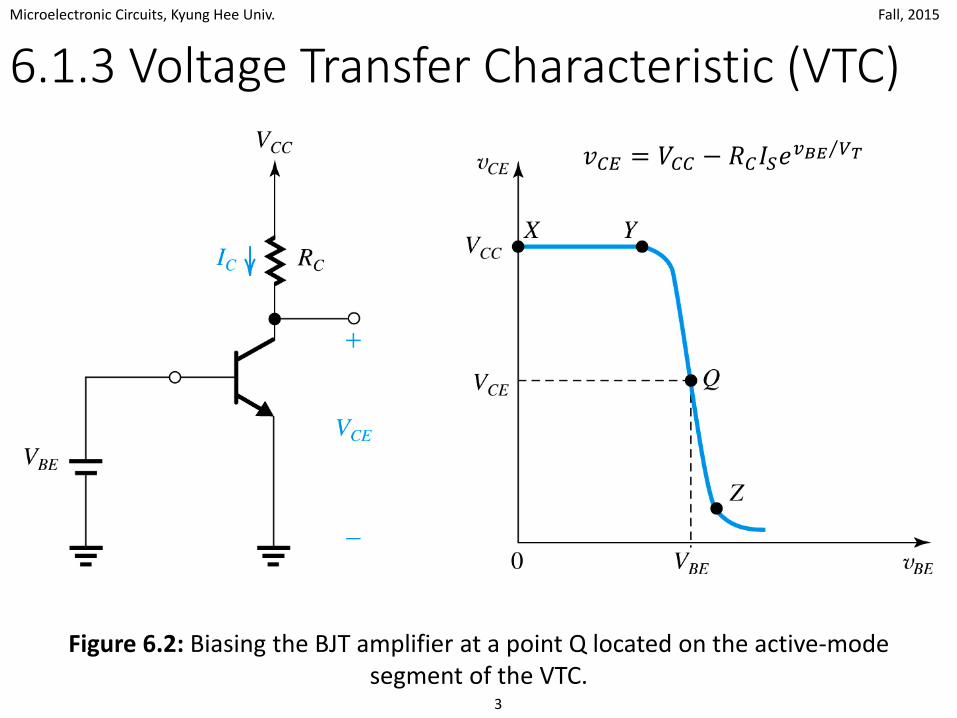
6.1.3 Voltage Transfer Characteristic (VTC)
Figure 6.2: Biasing the BJT amplifier at a point Q located on the active-mode segment of the VTC.
𝑣𝑣𝐶𝐶𝐶𝐶 = 𝑉𝑉𝐶𝐶𝐶𝐶 − 𝑅𝑅𝐶𝐶𝐼𝐼𝑆𝑆𝑒𝑒 ⁄𝑣𝑣𝐵𝐵𝐵𝐵 𝑉𝑉𝑇𝑇

Microelectronic Circuits, Kyung Hee Univ. Fall, 2015
4
6.1.4 Biasing the TransistorFigure 6.6: BJT amplifier biased at apoint Q (bias point/dc operating point)with a small voltage signal vbesuperimposed on the dc bias voltageVBE.
Microelectronic Circuits, Kyung Hee Univ. Fall, 2015
5
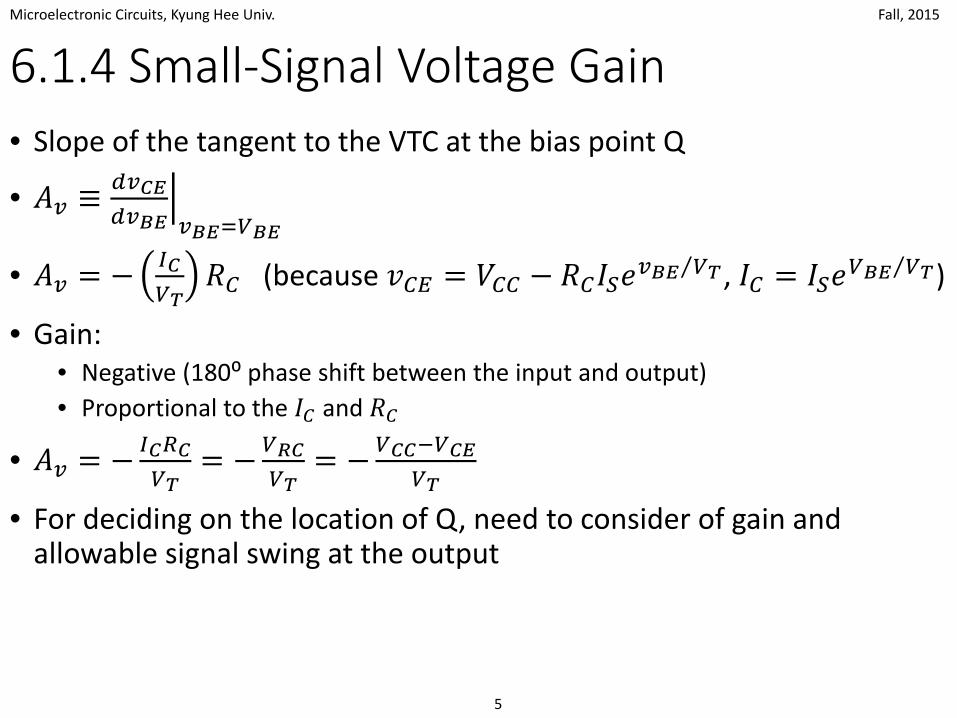
6.1.4 Small-Signal Voltage Gain• Slope of the tangent to the VTC at the bias point Q
• 𝐴𝐴𝑣𝑣 ≡ �𝑑𝑑𝑣𝑣𝐶𝐶𝐵𝐵𝑑𝑑𝑣𝑣𝐵𝐵𝐵𝐵 𝑣𝑣𝐵𝐵𝐵𝐵=𝑉𝑉𝐵𝐵𝐵𝐵
• 𝐴𝐴𝑣𝑣 = − 𝐼𝐼𝐶𝐶𝑉𝑉𝑇𝑇
𝑅𝑅𝐶𝐶 (because 𝑣𝑣𝐶𝐶𝐶𝐶 = 𝑉𝑉𝐶𝐶𝐶𝐶 − 𝑅𝑅𝐶𝐶𝐼𝐼𝑆𝑆𝑒𝑒 ⁄𝑣𝑣𝐵𝐵𝐵𝐵 𝑉𝑉𝑇𝑇, 𝐼𝐼𝐶𝐶 = 𝐼𝐼𝑆𝑆𝑒𝑒 ⁄𝑉𝑉𝐵𝐵𝐵𝐵 𝑉𝑉𝑇𝑇)
• Gain: • Negative (180⁰ phase shift between the input and output)• Proportional to the 𝐼𝐼𝐶𝐶 and 𝑅𝑅𝐶𝐶
• 𝐴𝐴𝑣𝑣 = − 𝐼𝐼𝐶𝐶𝑅𝑅𝐶𝐶𝑉𝑉𝑇𝑇
= −𝑉𝑉𝑅𝑅𝐶𝐶𝑉𝑉𝑇𝑇
= −𝑉𝑉𝐶𝐶𝐶𝐶−𝑉𝑉𝐶𝐶𝐵𝐵𝑉𝑉𝑇𝑇
• For deciding on the location of Q, need to consider of gain and allowable signal swing at the output
Microelectronic Circuits, Kyung Hee Univ. Fall, 2015
6
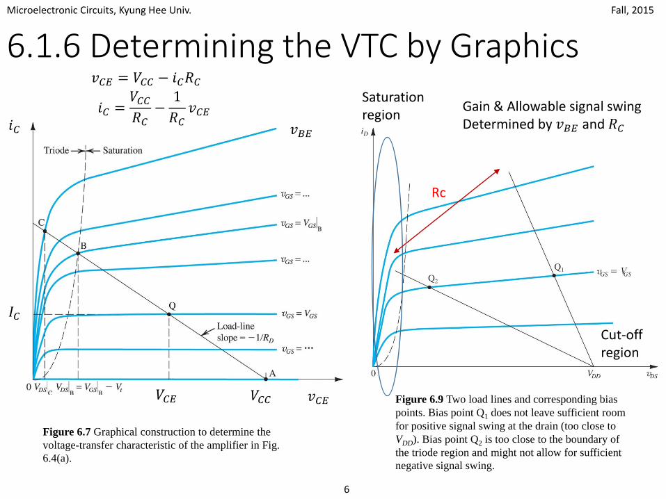
6.1.6 Determining the VTC by Graphics
𝐼𝐼𝐶𝐶
Figure 6.7 Graphical construction to determine the voltage-transfer characteristic of the amplifier in Fig. 6.4(a).
Figure 6.9 Two load lines and corresponding bias points. Bias point Q1 does not leave sufficient room for positive signal swing at the drain (too close to VDD). Bias point Q2 is too close to the boundary of the triode region and might not allow for sufficient negative signal swing.
𝑣𝑣𝐶𝐶𝐶𝐶 = 𝑉𝑉𝐶𝐶𝐶𝐶 − 𝑖𝑖𝐶𝐶𝑅𝑅𝐶𝐶
𝑖𝑖𝐶𝐶 =𝑉𝑉𝐶𝐶𝐶𝐶𝑅𝑅𝐶𝐶
−1𝑅𝑅𝐶𝐶
𝑣𝑣𝐶𝐶𝐶𝐶𝑣𝑣𝐵𝐵𝐶𝐶𝑖𝑖𝐶𝐶
𝑣𝑣𝐶𝐶𝐶𝐶𝑉𝑉𝐶𝐶𝐶𝐶𝑉𝑉𝐶𝐶𝐶𝐶
Saturationregion
Cut-offregion
Rc
Gain & Allowable signal swingDetermined by 𝑣𝑣𝐵𝐵𝐶𝐶 and 𝑅𝑅𝐶𝐶

Microelectronic Circuits, Kyung Hee Univ. Fall, 2015
7
6.2 Small-Signal Operation and Models
• 𝐼𝐼𝐶𝐶 = 𝐼𝐼𝑆𝑆𝑒𝑒 ⁄𝑉𝑉𝐵𝐵𝐵𝐵 𝑉𝑉𝑇𝑇
• 𝐼𝐼𝐶𝐶 = 𝐼𝐼𝐶𝐶/𝛼𝛼
• 𝐼𝐼𝐵𝐵 = 𝐼𝐼𝐶𝐶/β
• 𝑉𝑉𝐶𝐶𝐶𝐶 = 𝑉𝑉𝐶𝐶𝐶𝐶 − 𝐼𝐼𝐶𝐶𝑅𝑅𝐶𝐶• 𝑉𝑉𝐶𝐶 > 𝑉𝑉𝐵𝐵 − 0.4 𝑉𝑉

Microelectronic Circuits, Kyung Hee Univ. Fall, 2015
8
Collector Current / Transconductance• 𝑣𝑣𝐵𝐵𝐶𝐶 = 𝑉𝑉𝐵𝐵𝐶𝐶 + 𝑣𝑣𝑏𝑏𝑏𝑏• 𝑖𝑖𝐶𝐶 = 𝐼𝐼𝐶𝐶𝑒𝑒 ⁄𝑣𝑣𝑏𝑏𝑏𝑏 𝑉𝑉𝑇𝑇
• (𝑣𝑣𝑏𝑏𝑏𝑏 ≪ 𝑉𝑉𝑇𝑇)
• 𝑖𝑖𝐶𝐶 ≅ 𝐼𝐼𝐶𝐶(1 + 𝑣𝑣𝑏𝑏𝑏𝑏𝑉𝑉𝑇𝑇
) if 𝑣𝑣𝑏𝑏𝑏𝑏<10mV : small signal approximation
• 𝑖𝑖𝐶𝐶 = 𝐼𝐼𝐶𝐶 + 𝐼𝐼𝐶𝐶𝑉𝑉𝑇𝑇𝑣𝑣𝑏𝑏𝑏𝑏
• 𝑖𝑖𝑐𝑐 = 𝐼𝐼𝐶𝐶𝑉𝑉𝑇𝑇𝑣𝑣𝑏𝑏𝑏𝑏
• 𝑖𝑖𝑐𝑐 = 𝑔𝑔𝑚𝑚𝑣𝑣𝑏𝑏𝑏𝑏• 𝑔𝑔𝑚𝑚 = 𝐼𝐼𝐶𝐶
𝑉𝑉𝑇𝑇: trans-conductance
• Slope of 𝑖𝑖𝐶𝐶 − 𝑣𝑣𝑏𝑏𝑏𝑏 characteristic curve at 𝑖𝑖𝑐𝑐 = 𝐼𝐼𝐶𝐶
• Voltage controlled current source
• Output resistance: infinite• Finite output resistance due
to Early effect
Microelectronic Circuits, Kyung Hee Univ. Fall, 2015
9
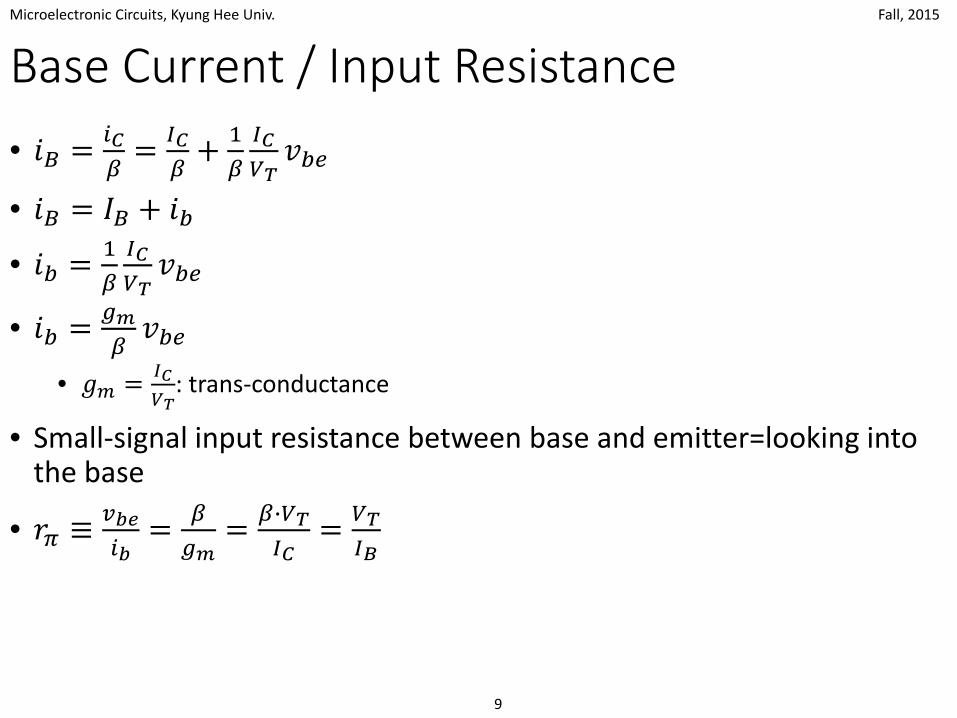
Base Current / Input Resistance• 𝑖𝑖𝐵𝐵 = 𝑖𝑖𝐶𝐶
𝛽𝛽= 𝐼𝐼𝐶𝐶
𝛽𝛽+ 1
𝛽𝛽𝐼𝐼𝐶𝐶𝑉𝑉𝑇𝑇𝑣𝑣𝑏𝑏𝑏𝑏
• 𝑖𝑖𝐵𝐵 = 𝐼𝐼𝐵𝐵 + 𝑖𝑖𝑏𝑏• 𝑖𝑖𝑏𝑏 = 1
𝛽𝛽𝐼𝐼𝐶𝐶𝑉𝑉𝑇𝑇𝑣𝑣𝑏𝑏𝑏𝑏
• 𝑖𝑖𝑏𝑏 = 𝑔𝑔𝑚𝑚𝛽𝛽𝑣𝑣𝑏𝑏𝑏𝑏
• 𝑔𝑔𝑚𝑚 = 𝐼𝐼𝐶𝐶𝑉𝑉𝑇𝑇
: trans-conductance
• Small-signal input resistance between base and emitter=looking into the base
• 𝑟𝑟𝜋𝜋 ≡𝑣𝑣𝑏𝑏𝑏𝑏𝑖𝑖𝑏𝑏
= 𝛽𝛽𝑔𝑔𝑚𝑚
= 𝛽𝛽�𝑉𝑉𝑇𝑇𝐼𝐼𝐶𝐶
= 𝑉𝑉𝑇𝑇𝐼𝐼𝐵𝐵

Microelectronic Circuits, Kyung Hee Univ. Fall, 2015
10
Emitter Current and Input Resistance• 𝑖𝑖𝐶𝐶 = 𝑖𝑖𝐶𝐶
𝛼𝛼= 𝐼𝐼𝐶𝐶
𝛼𝛼+ 𝑖𝑖𝑐𝑐
𝛼𝛼= 𝐼𝐼𝐶𝐶 + 𝑖𝑖𝑏𝑏
• 𝑖𝑖𝑏𝑏 = 𝑖𝑖𝑐𝑐𝛼𝛼
= 1𝛼𝛼𝐼𝐼𝐶𝐶𝑉𝑉𝑇𝑇𝑣𝑣𝑏𝑏𝑏𝑏 = 𝐼𝐼𝐵𝐵
𝑉𝑉𝑇𝑇𝑣𝑣𝑏𝑏𝑏𝑏
• Small-signal input resistance between base and emitter=looking into the emitter
• 𝑟𝑟𝑏𝑏 ≡𝑣𝑣𝑏𝑏𝑏𝑏𝑖𝑖𝑏𝑏
= 𝑉𝑉𝑇𝑇𝐼𝐼𝐵𝐵
= 𝛼𝛼𝑔𝑔𝑚𝑚
≅ 1𝑔𝑔𝑚𝑚
• 𝑣𝑣𝑏𝑏𝑏𝑏 = 𝑖𝑖𝑏𝑏𝑟𝑟𝜋𝜋 = 𝑖𝑖𝑏𝑏𝑟𝑟𝑏𝑏• 𝑟𝑟𝜋𝜋 = ⁄𝑖𝑖𝑏𝑏 𝑖𝑖𝑏𝑏 𝑟𝑟𝑏𝑏 = (𝛽𝛽 + 1)𝑟𝑟𝑏𝑏

Microelectronic Circuits, Kyung Hee Univ. Fall, 2015
11
Voltage Gain• 𝑣𝑣𝐶𝐶𝐶𝐶 = 𝑉𝑉𝐶𝐶𝐶𝐶 − 𝑖𝑖𝐶𝐶𝑅𝑅𝐶𝐶 = 𝑉𝑉𝐶𝐶𝐶𝐶 − 𝐼𝐼𝐶𝐶 + 𝑖𝑖𝑐𝑐 𝑅𝑅𝐶𝐶 = 𝑉𝑉𝐶𝐶𝐶𝐶 − 𝐼𝐼𝐶𝐶𝑅𝑅𝐶𝐶 − 𝑖𝑖𝑐𝑐𝑅𝑅𝐶𝐶• = 𝑉𝑉𝐶𝐶𝐶𝐶−𝑖𝑖𝑐𝑐𝑅𝑅𝐶𝐶• 𝑣𝑣𝑐𝑐𝑏𝑏 = −𝑖𝑖𝑐𝑐𝑅𝑅𝐶𝐶 = −𝑔𝑔𝑚𝑚𝑣𝑣𝑏𝑏𝑏𝑏𝑅𝑅𝐶𝐶 = (−𝑔𝑔𝑚𝑚𝑅𝑅𝐶𝐶)𝑣𝑣𝑏𝑏𝑏𝑏• Voltage gain of this amplifier 𝐴𝐴𝑣𝑣• 𝐴𝐴𝑣𝑣 ≡
𝑣𝑣𝑐𝑐𝑏𝑏𝑣𝑣𝑏𝑏𝑏𝑏
= −𝑔𝑔𝑚𝑚𝑅𝑅𝐶𝐶 = − 𝐼𝐼𝐶𝐶𝑅𝑅𝐶𝐶𝑉𝑉𝑇𝑇
Separating Signal/DC• Replaced 𝑉𝑉𝐶𝐶𝐶𝐶 and 𝑉𝑉𝐵𝐵𝐶𝐶 with short circuits• Current increments (𝑖𝑖𝑐𝑐, 𝑖𝑖𝑏𝑏, and 𝑖𝑖𝑏𝑏) obtained
when a small signal 𝑣𝑣𝑏𝑏𝑏𝑏 is applied• Considered an equivalent small-signal circuit
model
Figure 6.23 The amplifier circuit of Fig. 6.20(a) with the dc sources (VBE and VCC) eliminated (short-circuited). Thus only the signal components are present. Note that this is a representation of the signal operation of the BJT and not an actual amplifier circuit.

Microelectronic Circuits, Kyung Hee Univ. Fall, 2015
12
Hybrid-π Model• Voltage controlled current source• Input resistance looking into the base, 𝑟𝑟𝜋𝜋• 𝑖𝑖𝑐𝑐 = 𝑔𝑔𝑚𝑚𝑣𝑣𝑏𝑏𝑏𝑏 and 𝑖𝑖𝑏𝑏 = 𝑣𝑣𝑏𝑏𝑏𝑏
𝑟𝑟𝜋𝜋
• 𝑖𝑖𝑏𝑏 = 𝑣𝑣𝑏𝑏𝑏𝑏𝑟𝑟𝜋𝜋
+ 𝑔𝑔𝑚𝑚𝑣𝑣𝑏𝑏𝑏𝑏 = 𝑣𝑣𝑏𝑏𝑏𝑏𝑟𝑟𝜋𝜋
1 + 𝑔𝑔𝑚𝑚𝑟𝑟𝜋𝜋 = 𝑣𝑣𝑏𝑏𝑏𝑏𝑟𝑟𝜋𝜋
1 + 𝛽𝛽 = �𝑣𝑣𝑏𝑏𝑏𝑏𝑟𝑟𝜋𝜋1+𝛽𝛽
= 𝑣𝑣𝑏𝑏𝑏𝑏𝑟𝑟𝑏𝑏
• 𝑔𝑔𝑚𝑚𝑣𝑣𝑏𝑏𝑏𝑏 = 𝑔𝑔𝑚𝑚 𝑖𝑖𝑏𝑏𝑟𝑟𝜋𝜋 = 𝑔𝑔𝑚𝑚𝑟𝑟𝜋𝜋 𝑖𝑖𝑏𝑏 = 𝛽𝛽𝑖𝑖𝑏𝑏
Figure 6.24 Two slightly different versions of the hybrid-π model for the small-signal operation of the BJT. The equivalent circuit in (a) represents the BJT as a voltage-controlled current source (a transconductance amplifier), and that in (b) represents the BJT as a current-controlled current source (a current amplifier).

Microelectronic Circuits, Kyung Hee Univ. Fall, 2015
13
T Model• Voltage controlled current source with control
voltage being 𝑣𝑣𝑏𝑏𝑏𝑏• Resistance between base and emitter, looking
into the base, 𝑟𝑟𝑏𝑏• 𝑖𝑖𝑏𝑏 = 𝑣𝑣𝑏𝑏𝑏𝑏
𝑟𝑟𝑏𝑏− 𝑔𝑔𝑚𝑚𝑣𝑣𝑏𝑏𝑏𝑏 = 𝑣𝑣𝑏𝑏𝑏𝑏
𝑟𝑟𝑏𝑏1 − 𝑔𝑔𝑚𝑚𝑟𝑟𝑏𝑏 =
𝑣𝑣𝑏𝑏𝑏𝑏𝑟𝑟𝑏𝑏
1 − 𝛼𝛼 = 𝑣𝑣𝑏𝑏𝑏𝑏𝑟𝑟𝑏𝑏
1 − 𝛽𝛽𝛽𝛽+1
= 𝑣𝑣𝑏𝑏𝑏𝑏(𝛽𝛽+1)𝑟𝑟𝑏𝑏
= 𝑣𝑣𝑏𝑏𝑏𝑏𝑟𝑟𝜋𝜋
• 𝑔𝑔𝑚𝑚𝑣𝑣𝑏𝑏𝑏𝑏 = 𝑔𝑔𝑚𝑚 𝑖𝑖𝑏𝑏𝑟𝑟𝑏𝑏 = 𝑔𝑔𝑚𝑚𝑟𝑟𝑏𝑏 𝑖𝑖𝑏𝑏 = 𝛼𝛼𝑖𝑖𝑏𝑏• Example 6.5~6.7
Figure 6.26 Two slightly different versions of what is known as the T model of the BJT. The circuit in (a) is a voltage-controlled current source representation and that in (b) is a current-controlled current source representation. These models explicitly show the emitter resistance re rather than the base resistance rπ featured in the hybrid-π model.

Microelectronic Circuits, Kyung Hee Univ. Fall, 2015
14
Performing Small-Signal Analysis
Figure 6.32 Performing signal analysis directly on the circuit diagram with the BJT small-signal model implicitly employed:
(a) circuit for Example 6.5; (b) circuit for Example 6.7.

Microelectronic Circuits, Kyung Hee Univ. Fall, 2015
15
Summary

Microelectronic Circuits, Kyung Hee Univ. Fall, 2015
16