Embed Size (px)
Citation preview

© April 25, 2012 Dr. Lynn Fuller
Rochester Institute of Technology
Microelectronic Engineering
MEMs Unit Processes - Measurement
Page 1
ROCHESTER INSTITUTE OF TEHNOLOGYMICROELECTRONIC ENGINEERING
4-25-2012 mem_meas.ppt
Microelectromechanical Systems (MEMs)Unit Processes for MEMs
Measurement
Dr. Lynn FullerWebpage: http://people.rit.edu/lffeee
Microelectronic EngineeringRochester Institute of Technology
82 Lomb Memorial DriveRochester, NY 14623-5604
Tel (585) 475-2035Fax (585) 475-5041
Email: [email protected] webpage: http://www.microe.rit.edu

© April 25, 2012 Dr. Lynn Fuller
Rochester Institute of Technology
Microelectronic Engineering
MEMs Unit Processes - Measurement
Page 2
OUTLINE
Visual Inspection Optical MicroscopyElectron Microscopy
LinewidthThicknessEtch RateResistivity and Sheet ResistanceSelectivityStressReferencesHomework

© April 25, 2012 Dr. Lynn Fuller
Rochester Institute of Technology
Microelectronic Engineering
MEMs Unit Processes - Measurement
Page 3
Bright Field Dark FieldSelection mechanism
TV Camera
Focus and height measurement each division is 1 µm
x-y stage movement
Objective lenses, 5X, 10X, 40X, 100X
Tri-nocular Eyepiece and Camera Mount
Stage
ApertureFilters
Coaxial Illuminator
Illuminator forTransparent Samples
OPTICAL MICROSCOPY

© April 25, 2012 Dr. Lynn Fuller
Rochester Institute of Technology
Microelectronic Engineering
MEMs Unit Processes - Measurement
Page 4
OPTICAL PICTURE OF ETCH PIT
20% KOH <100> Si Etch - 16 Hrs. @ 72C

© April 25, 2012 Dr. Lynn Fuller
Rochester Institute of Technology
Microelectronic Engineering
MEMs Unit Processes - Measurement
Page 5
PHILLIPS SEM

© April 25, 2012 Dr. Lynn Fuller
Rochester Institute of Technology
Microelectronic Engineering
MEMs Unit Processes - Measurement
Page 6
SEM PICTURES
These SEM pictures show typical profiles of aluminum over steps from the CVC601.

© April 25, 2012 Dr. Lynn Fuller
Rochester Institute of Technology
Microelectronic Engineering
MEMs Unit Processes - Measurement
Page 7
Surface~ 100 Å Gap
Piezoelectric Motors Scan Tip in X and Y, Electronics control Z such that the Tunneling Current I is Constant. The Control Voltage for Z is a Measure of Surface Topology
X
YZ
I
SCANNING TUNNELING MICROSCOPE (STM)

© April 25, 2012 Dr. Lynn Fuller
Rochester Institute of Technology
Microelectronic Engineering
MEMs Unit Processes - Measurement
Page 8
ATOMIC FORCE MICROSCOPE (AFM)

© April 25, 2012 Dr. Lynn Fuller
Rochester Institute of Technology
Microelectronic Engineering
MEMs Unit Processes - Measurement
Page 9
ATOMIC FORCE MICROSCOPE (AFM)
� Standard Sharp Apex Slender Long Used in Contact mode
� CD Mode (Conical and Flared)
Flared tip able to measure undercut sidewalls
Used in non-contact mode

© April 25, 2012 Dr. Lynn Fuller
Rochester Institute of Technology
Microelectronic Engineering
MEMs Unit Processes - Measurement
Page 10
LINEWIDTH MEASUREMENT
Calibrate the output device for the microscope for a known size object. Then display unknown device and determine size by comparing the unknown to the known size.
A filar eyepiece is an eyepiece with a mechanical dial that moves a hairline across the field of view. The markings on the dial are calibrated by measuring a known size object. Unknown size objects are measured by positioning the hairline on one edge of the object, reading the dial and positioning the hairline on the other side of the object and reading the difference. Then calculating the size knowing the calibration. This technique is limited to objects small enough to fit within the field of view. For larger objects a calibrated traveling stage with a fixed hairline within the eyepiece can be used. Newer systems use CCD camera pixel counting rather than a mechanical eyepiece.

© April 25, 2012 Dr. Lynn Fuller
Rochester Institute of Technology
Microelectronic Engineering
MEMs Unit Processes - Measurement
Page 11
LINEWIDTH MEASUREMENT SYSTEM

© April 25, 2012 Dr. Lynn Fuller
Rochester Institute of Technology
Microelectronic Engineering
MEMs Unit Processes - Measurement
Page 12
Dial divisions are 0.001 inch units equal to 25.4 µm accuracy is about 1/2 division or 12.5 µm, this is good for measuring thickness in the 100’s of microns range
Focus and height measurement each divisionis 1 µm
HEIGHT MEASUREMENT USING OPTICAL MICROSCOPE

© April 25, 2012 Dr. Lynn Fuller
Rochester Institute of Technology
Microelectronic Engineering
MEMs Unit Processes - Measurement
Page 13
HEIGHT MEASUREMENT USING OPTICAL MICROSCOPE
Put object on the microscope and obtain an image then place the micrometer under the stage as shown to measure the height change as the focus knob is turned
Use the 100 x Objective Lens for smallest depth of focus
Focus on top of object and set micrometer dial to zero
Focus on bottom of objectand read the height on themicrometer dial.

© April 25, 2012 Dr. Lynn Fuller
Rochester Institute of Technology
Microelectronic Engineering
MEMs Unit Processes - Measurement
Page 14
OPTICAL TECHNIQUES FOR HEIGHT AND DISPLACEMENT
http://www.veeco.com
3D Surface TopographyHeights 0.1 nm to 5 mmResolution 0.1 nm

© April 25, 2012 Dr. Lynn Fuller
Rochester Institute of Technology
Microelectronic Engineering
MEMs Unit Processes - Measurement
Page 15
RIT’s VEECO WYCO NT1100 OPTICAL PROFILOMETER
Used to measure RMS surface roughness

© April 25, 2012 Dr. Lynn Fuller
Rochester Institute of Technology
Microelectronic Engineering
MEMs Unit Processes - Measurement
Page 16
VEECO DYNAMIC OPTICAL PROFILER

© April 25, 2012 Dr. Lynn Fuller
Rochester Institute of Technology
Microelectronic Engineering
MEMs Unit Processes - Measurement
Page 17
SURFACE ROUGHNESS DATA
~5nm RMS
~15nm RMS
Bare Silicon Wafer
Aluminum CVC 601 – 6800Å
© April 25, 2012 Dr. Lynn Fuller
Rochester Institute of Technology
Microelectronic Engineering
MEMs Unit Processes - Measurement
Page 18
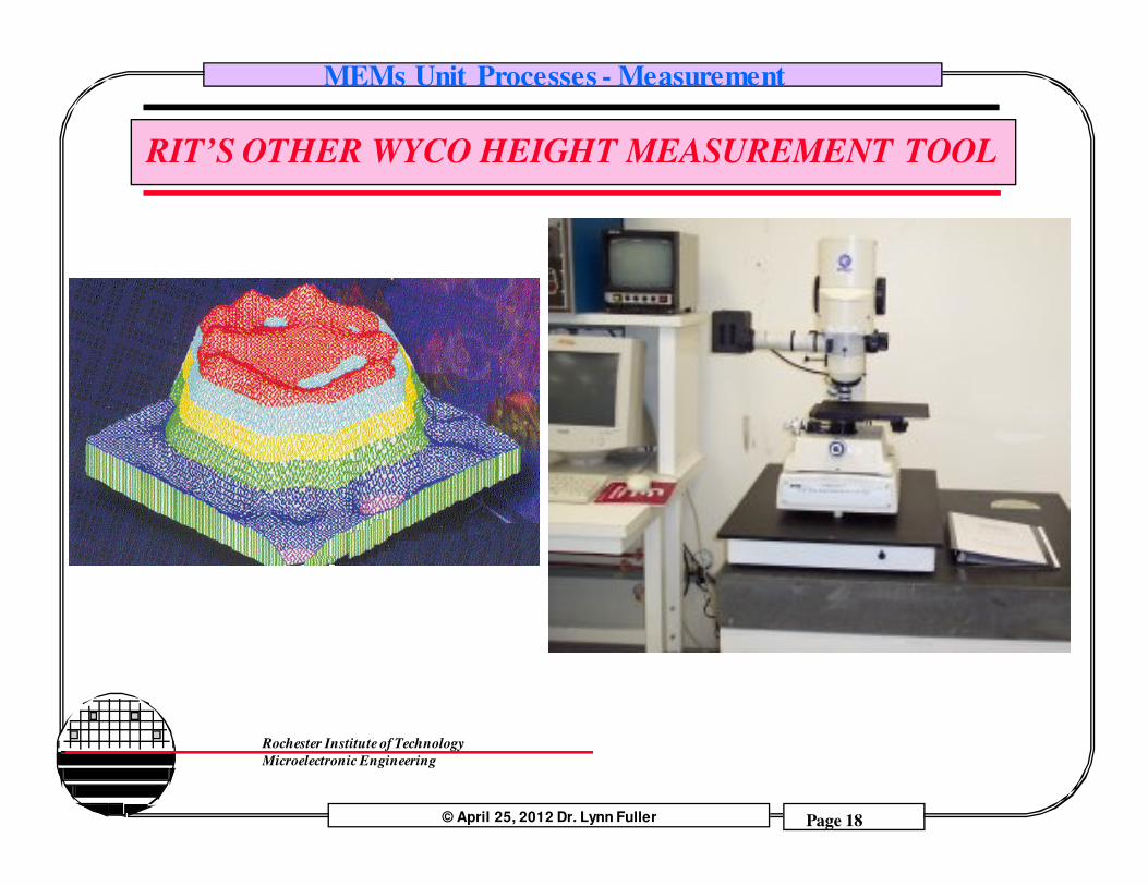
RIT’S OTHER WYCO HEIGHT MEASUREMENT TOOL

© April 25, 2012 Dr. Lynn Fuller
Rochester Institute of Technology
Microelectronic Engineering
MEMs Unit Processes - Measurement
Page 19
HEIGHT MEASUREMENT USING OPTICAL MICROSCOPE
20% KOH Etch, @ 72 C, 10 Hrs.
31 µm500 µm

© April 25, 2012 Dr. Lynn Fuller
Rochester Institute of Technology
Microelectronic Engineering
MEMs Unit Processes - Measurement
Page 20
TENCORE P2 LONG SCAN PROFILOMETER

© April 25, 2012 Dr. Lynn Fuller
Rochester Institute of Technology
Microelectronic Engineering
MEMs Unit Processes - Measurement
Page 21
0
10
Film Thickness
Readout
Stylus
Film
STYLUS SURFACE PROFILOMETER
1,000 Å < Max < 1,000,000 Å

© April 25, 2012 Dr. Lynn Fuller
Rochester Institute of Technology
Microelectronic Engineering
MEMs Unit Processes - Measurement
Page 22
OXIDE THICKNESS COLOR CHART
X other materials = Xoxide 1.45/nother material
Thickness Color Thickness Color
500 Tan 4900 Blue
700 Brown 5000 Blue Green
1000 Dark Violet - Red Violet 5200 Green
1200 Royal Blue 5400 Yellow Green
1500 Light Blue - Metallic Blue 5600 GreenYellow
1700 Metallic - very light Yellow Green 5700 Yel low -"Yel lowish"(at times appears to be Lt gray or matellic)
2000 LIght Gold or Yellow - Slightly Metallic 5800 Light Orange or Yellow - Pink
2200 Gold with slight Yellow Orange 6000 Carnation Pink
2500 Orange - Melon 6300 Violet Red
2700 Red Violet 6800 "Bluish"(appears violet red, Blue Green, looks gray ish)
3000 Blue - Violet Blue 7200 Blue Green - Green
3100 Blue 7700 "Yellowish"
3200 Blue - Blue Green 8000 Orange
3400 Light Green 8200 Salmon
3500 Green - Yellow Green 8500 Dull, LIght Red Violet
3600 Yellow Green 8600 Violet
3700 Yellow 8700 Blue Violet
3900 Light Orange 8900 Blue
4100 Carnation Pink 9200 Blue Green
4200 Violet Red 9500 Dull Yellow Green
4400 Red Violet 9700 Yellow - "Yellowish"
4600 Violet 9900 Orange
4700 Blue Violet 10000 Carnation Pink
Blue
Blue
Blue
Blue
Blue
Nitride Thickness = (Oxide Thickness)(Oxide Index/Nitride Index)Eg. Yellow Nitride Thickness = (2000)(1.46/2.00) = 1460

© April 25, 2012 Dr. Lynn Fuller
Rochester Institute of Technology
Microelectronic Engineering
MEMs Unit Processes - Measurement
Page 23
INCIDENT WHITE LIGHT, THE INTENSITY OF THEREFLECTED LIGHT IS MEASURED VS WAVELENGTH
WHITE LIGHT SOURCE
OPTICS
WAFER
MONOCHROMATOR& DETECTOR
(REFLECTANCE SPECTROMETER)NANOSPEC THICKNESS MEASUREMENT
λλλλ
3000 Å OXIDE
λλλλ
7000 Å OXIDE
Oxide on Silicon 400-30,000 ÅNitride 400-30,000Neg Resist 500-40,000Poly on 300-1200 Ox 400-10,000Neg Resist on Ox 300-350 300-3500Nitride on Oxide 300-3500 300-3500Thin Oxide 100-500Thin Nitride 100-500Polyimide 500-10,000Positive Resist 500-40,000Pos Resist on Ox 500-15,000 4,000-30,000

© April 25, 2012 Dr. Lynn Fuller
Rochester Institute of Technology
Microelectronic Engineering
MEMs Unit Processes - Measurement
Page 24
NANOSPEC FILM THICKNESS MEASUREMENT TOOL

© April 25, 2012 Dr. Lynn Fuller
Rochester Institute of Technology
Microelectronic Engineering
MEMs Unit Processes - Measurement
Page 25
TENCORE SPECROMAP
Record:
MeanStd DeviationMinMaxNo of Points

© April 25, 2012 Dr. Lynn Fuller
Rochester Institute of Technology
Microelectronic Engineering
MEMs Unit Processes - Measurement
Page 26
PHOTODETECTOR
The light source is unpolarized, upon traversing the polarizer the light becomes linearly polarized. Turning the polarizer adjusts the azimuth of linearly polarized light with respect to the fast axis of the quarter-wave plate in such a way as to vary the e llipticity of the light incident on the surface. This ellipticity is adjusted until it is just cancelled by the e llipticity introduced by the reflection. The result is again linearly polarized light. The analyzer polarizing prism is rotated until its axis of polarization is perpendicular to the azimuth of the linearly polarized light, creating a null. Thus no light is transmitted to the dedector. The common technique is to fix the quarter-wave plate with fast axis at 45 ° to the plane of incidence, and to alternately move the polarizer and analyzer, continuously reducing the transmitted light until a null is reached. The relevant light parameters ∆∆∆∆ and Ψ Ψ Ψ Ψ are readily calculated from the instrument parameters (P, polarizer angle, Q, quarter-wave plate angle, and A, analyzer angle. Values for film thickness and index of refraction are found. Thickness values that correspond to these parameters repeat with multiples of the light source wavelength so the approximate thickness must be known.
SURFACE
FILTER (blockes out room light)
LIGHTSOURCE
POLARIZER
QUARTER WAVEPLATE ANALYZER
unpolarized
ellipticpolarized
nulllinear polarized
linear
ELLIPSOMETRY

© April 25, 2012 Dr. Lynn Fuller
Rochester Institute of Technology
Microelectronic Engineering
MEMs Unit Processes - Measurement
Page 27
ELLIPSOMETER
Rudolph EllipsometerVariable Angle Spectroscopic
Ellipsometer

© April 25, 2012 Dr. Lynn Fuller
Rochester Institute of Technology
Microelectronic Engineering
MEMs Unit Processes - Measurement
Page 28
MN
After Stain Xj = (N * M) / D(at RIT D=1.532 inch)
D
Groove
Staining Solution - 1 Vol part HF, 2 Vol part Nitric Acid, 12 Vol part Acetic AcidAfter mixing drop a penny in solution for about 10 sec. result in a light bluecolor. Safety Stain - (does not have HF) is available from Philtec InstrumentCo. Philadelphia, PA 19129-1651, (215) 848-4500, Signatone makes groove tool
and wheels, (408)732-3280
MN
GROOVE and STAIN FIND Xj AFTER PRE DEPOSIT OR DRIVE-IN

© April 25, 2012 Dr. Lynn Fuller
Rochester Institute of Technology
Microelectronic Engineering
MEMs Unit Processes - Measurement
Page 29
TRAVELING STAGE MICROSCOPE
Example: If M=.003 inches and N=0.025 inches, find xj.
Poly on Oxide on Silicon(no stain)
Xj = (N * M) / D
= (0.025 * 0.003)/1.532 inch)= 0.0000472 inch= 1.20 µm

© April 25, 2012 Dr. Lynn Fuller
Rochester Institute of Technology
Microelectronic Engineering
MEMs Unit Processes - Measurement
Page 30
DEPTH WITH TRAVELING STAGE MICROSCOPE
KOH etches silicon along the (111) crystal plane giving a 53° angle.
100µm
Example: the traveling stagemicroscope is used to measurethe 100 µm distance shown. The depth is calculated.
Tan 53° = depth/100µmdepth = 133 µm

© April 25, 2012 Dr. Lynn Fuller
Rochester Institute of Technology
Microelectronic Engineering
MEMs Unit Processes - Measurement
Page 31
5000 Å
BARE SILICON
ETCH STEPS IN OXIDE TO FIND ETCH RATE

© April 25, 2012 Dr. Lynn Fuller
Rochester Institute of Technology
Microelectronic Engineering
MEMs Unit Processes - Measurement
Page 32
BUFFERED HF
Lower 1/4 inch every 45 seconds
STEP ETCH APPARATUS

© April 25, 2012 Dr. Lynn Fuller
Rochester Institute of Technology
Microelectronic Engineering
MEMs Unit Processes - Measurement
Page 33
VI
4PT PROBE
Rhos = V / I * ππππ / ln 2 = 4.532 V/I ohms/squareRho = Rhos Xj ohm-cm
Xj = (N * M) / D
D
Groove
Xj
M N
MN
After Stain
S
Xj
GROOVE AND STAIN AND 4PTPROBE FIND SHEET RESISTANCE AND RESISTIVITY FOR A DIFFUSED LAYER

© April 25, 2012 Dr. Lynn Fuller
Rochester Institute of Technology
Microelectronic Engineering
MEMs Unit Processes - Measurement
Page 34
FOUR POINT PROBE
V
I
S = probe spacing
W = wafer thickness
Rho = ππππ/ln2 x W x V / I ohm-cmif S<<W and S<<Wafer Diameter
FOUR POINT PROBE - RESISTIVITY

© April 25, 2012 Dr. Lynn Fuller
Rochester Institute of Technology
Microelectronic Engineering
MEMs Unit Processes - Measurement
Page 35
4 PT PROBE METAL THICKNESS MEASUREMENTS
CDE ResistivityMapper
Rho=Rhos x t
Tool gives Rho or Rhos depending on recipe used, automatically adjusts correction factors for wafer thickness
t = Rho/Rhos

© April 25, 2012 Dr. Lynn Fuller
Rochester Institute of Technology
Microelectronic Engineering
MEMs Unit Processes - Measurement
Page 36
SPUTTERED ALUMINUM THICKNESS UNIFORMITY
Ave = 6.03KMin = 4.73KMax = 7.68KNon Uniformity = 23.78%
CVC601

© April 25, 2012 Dr. Lynn Fuller
Rochester Institute of Technology
Microelectronic Engineering
MEMs Unit Processes - Measurement
Page 37
STRESS IN POLY AND NITRIDE FILMS
Test Structures for Measuring stress in Silicon Nitride Films

© April 25, 2012 Dr. Lynn Fuller
Rochester Institute of Technology
Microelectronic Engineering
MEMs Unit Processes - Measurement
Page 38
LOW STRESS SILICON RICH Si3N4
ADE Measured stress for various Ammonia: Dichlorosilane Flow Ratios
Flow Stress x E 9 dynes/cm210:1 +14.635:1 +14.812.5:1 +12.47 Stress: σσσσ = (E/(6(1-v)))*(D2/(rt))1:1 +10.13 where E is Youngs modulus, 1:2.5 +7.79* v is Poissons ratio, 1:5 +3 D and t are substrate and film thickness1:10 0 r is radius of curvature (- for tensile)*standard recipe
T.H Wu, “Stress in PSG and Nitride Films as Related to Film Properties and Annealing”, Solid State Technology, p 65-71,May ‘92
10 dyne/cm2 = 1 newton/m2 = 1 Pascal

© April 25, 2012 Dr. Lynn Fuller
Rochester Institute of Technology
Microelectronic Engineering
MEMs Unit Processes - Measurement
Page 39
REFERENCES
1. Mechanics of Materials, by Ferdinand P. Beer, E. Russell Johnston, Jr., McGraw-Hill Book Co.1981, ISBN 0-07-004284-5
2. “Etch Rates for Micromachining Processing”, Journal of Microelectromechanical Systems, Vol.5, No.4, December 1996.
3. “Crystalline Semiconductor Micromachine”, Seidel, Proceedings of the 4th Int. Conf. on Solid State Sensors and Actuators 1987, p 104
4. Optical height measurements, http://www.keyence.comhttp://www.veeco.com

© April 25, 2012 Dr. Lynn Fuller
Rochester Institute of Technology
Microelectronic Engineering
MEMs Unit Processes - Measurement
Page 40
HOMEWORK - MEASUREMENTS FOR MEMS
1. Derive the equation used in the groove and stain technique for measuring junction depth.
2. Describe 5 ways to estimate/measure the thickness of a polysilicon film that you deposit.
3. How does the nanospec work? What is the difference in its operation for thin oxides compared to thicker oxides? Why?