Embed Size (px)
Citation preview

Microcontroller: Timers, ADC
Amarjeet Singh
February 1, 2013

Logistics
2
Please share the JTAG and USB cables for your assignment Lecture tomorrow by Nipun

Revision from last class
3
When servicing an interrupt, how does the timing work? How are interrupt priorities decided? What are the primary blocks in a Timer/Counter? How is Buffer Value (BV) flag decided in both Capture and Compare
mode in xMega?

4
xMega: Timer/Counter Block Diagram
Registers: Counter (CNT), Period (PER), Compare Capture (CCx)
Size?
Counter compared with 0 or PER to generate BOTTOM/TOP
Compared with CCx to generate interrupt, events
Waveform generator mode uses CCx to set waveform period and pulse width
How to support 32 bit count?

5
Single Slope PWM Generation
Time period is controlled by PER register (counter counts from BOTTOM to TOP) while CCx register controls the duty cycle
New value of CCx Register loaded on UPDATE event WG output is set to 0 on compare match and set to 1 on TOP

6
Dual Slope PWM Generation
Time period is controlled by PER register (counter counts from BOTTOM to TOP and then TOP to BOTTOM) while CCx register controls the duty cycle
WG output is set to 1 on BOTTOM ; 0 on compare match during up count and 1 on compare match during down count
New value of CCx updated on UPDATE event

7
Timer/Counter 0/1: Associated Registers

8
Timer/Counter 0/1: Associated Registers
9
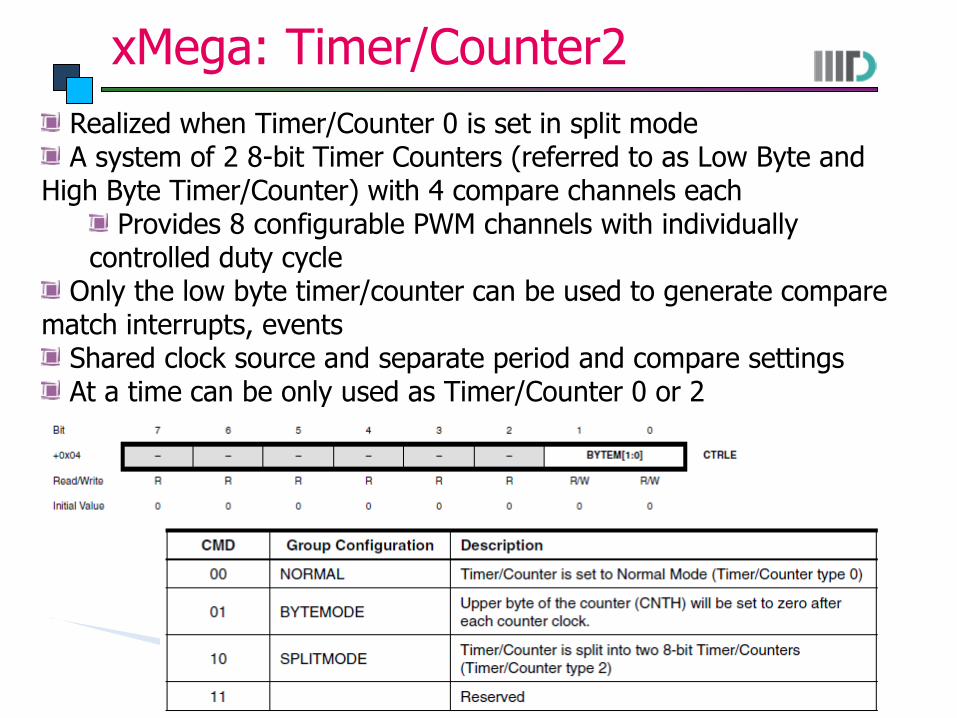
xMega: Timer/Counter2
Realized when Timer/Counter 0 is set in split mode A system of 2 8-bit Timer Counters (referred to as Low Byte and
High Byte Timer/Counter) with 4 compare channels each Provides 8 configurable PWM channels with individually
controlled duty cycle Only the low byte timer/counter can be used to generate compare
match interrupts, events Shared clock source and separate period and compare settings At a time can be only used as Timer/Counter 0 or 2
10
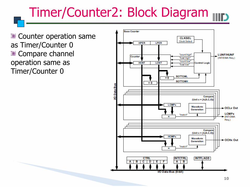
Timer/Counter2: Block Diagram
Counter operation same as Timer/Counter 0
Compare channel operation same as Timer/Counter 0

11
xMega Timers: Summary
TC-0/1: 16-bits, 32-bits support by cascading TC-2: 2 8-bits Multiple compare or capture (CC) channels for each timer
One compare match or input capture interrupt/event per channel
Used for count and direction control, capture Waveform generation:
Frequency generation Single slope PWM (Only this one available for TC-2) Dual slope PWM
Input capture: Frequency capture Pulse-width capture
12
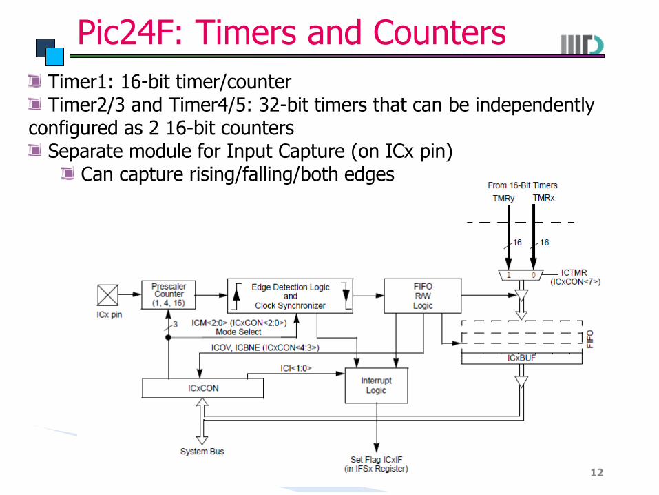
Pic24F: Timers and Counters
Timer1: 16-bit timer/counter Timer2/3 and Timer4/5: 32-bit timers that can be independently
configured as 2 16-bit counters Separate module for Input Capture (on ICx pin)
Can capture rising/falling/both edges

13
Pic24F: Timers and Counters
Separate output compare module to generate output pulses

14
AVR32: Timers and Counters

15
xMega: Real Time Counter (RTC)
16-bit RTC runs continuously even in the low power sleep mode to keep track of time
Can wake up devices from sleep and/or generate interrupt at regular
time intervals
Reference clock is typically 1.024KHz output from high accuracy crystal of 32.768 KHz
Includes a 10-bit prescaler to scale down the reference clock before it
reaches the counter
What is the highest resolution with 32.768 KHz clock? With a resolution of 1 s what is the maximum timeout period?

16
xMega: Real Time Counter (RTC)
RTC can generate both interrupts and events Compare interrupt Overflow interrupt

17
xMega: RTC32
32-bit Real Time Counter Runs continuously even in low power sleep mode External 32.768 KHz clock must be used as clock reference fed into
the prescaler Reference clock: 1 Hz or 1.024 KHz

18
PIC24F: Real Time Clock and Calendar
Time (hours, minutes, seconds); Calendar (Weekday, date, month, year): Year range 2000 – 2099 (with leap year correction)
Requires external 32.768 KHz clock crystal Optimized for low power operation

19
xMega: Analog Comparators
Compares voltage levels on two inputs and gives a digital output based on the comparison
Input sources: Analog port pins, several internal signals, 64-level programmable voltage scales the input values on positive pin AIN0 and negative pin AIN1
20
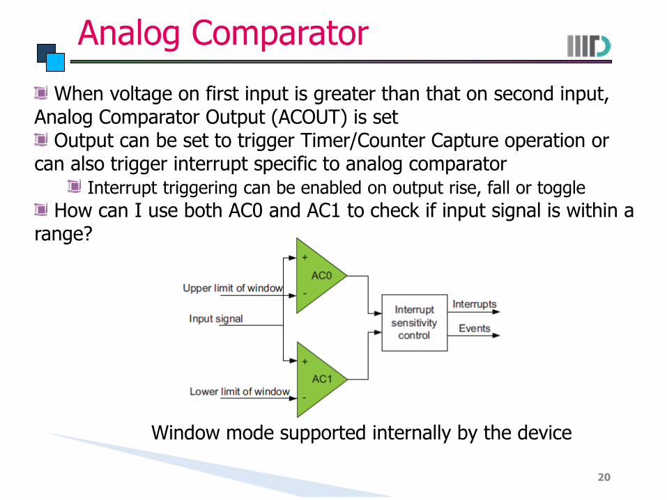
Analog Comparator
When voltage on first input is greater than that on second input, Analog Comparator Output (ACOUT) is set
Output can be set to trigger Timer/Counter Capture operation or can also trigger interrupt specific to analog comparator
Interrupt triggering can be enabled on output rise, fall or toggle How can I use both AC0 and AC1 to check if input signal is within a
range?
Window mode supported internally by the device
21
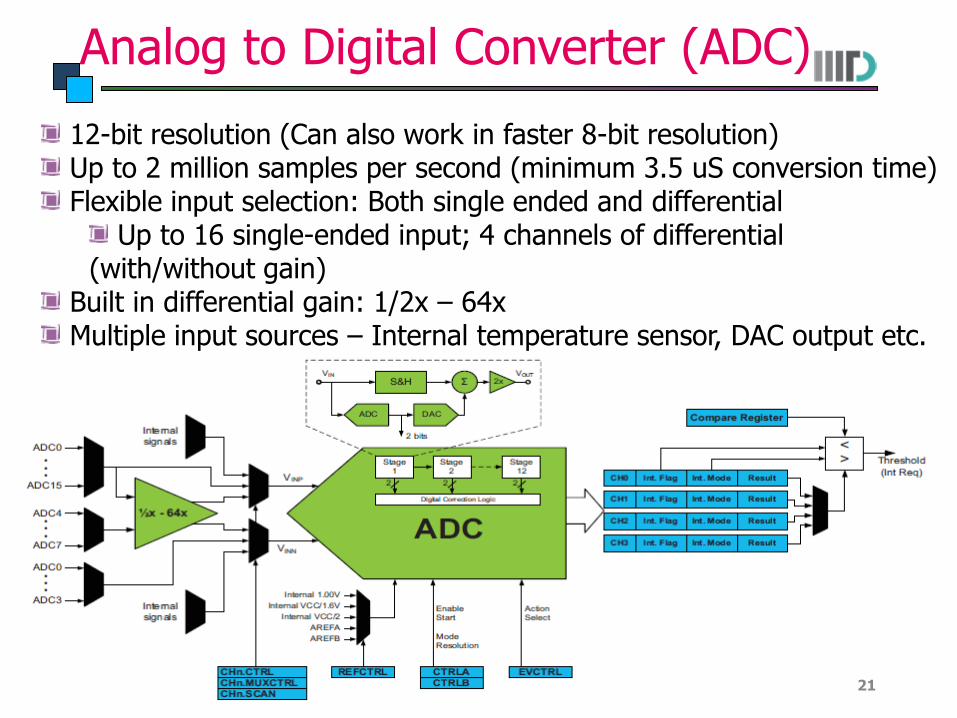
Analog to Digital Converter (ADC)
12-bit resolution (Can also work in faster 8-bit resolution) Up to 2 million samples per second (minimum 3.5 uS conversion time) Flexible input selection: Both single ended and differential
Up to 16 single-ended input; 4 channels of differential (with/without gain)
Built in differential gain: 1/2x – 64x Multiple input sources – Internal temperature sensor, DAC output etc.

22
Analog to Digital Converter (ADC)
Pipelined architecture with several stages: Allows high sample rate at low system clock frequency
New input can be sampled while older ADC conversions still going on
4 conversion channels with individual input selection: Allow 4 parallel operations

23
ADC Voltage Conversion
Several sources for reference voltage selection
Result is written to corresponding Channel result register (RES) Global setting for signed/unsigned conversion
Unsigned for single ended or internal signals Signed for differential signals generating both positive and
negative results What will be the TOP value for signed/unsigned conversion? What will be the ADC transfer function in terms of TOP?

24
ADC Voltage Conversion: Signed mode
Single ended measurement in signed mode: Negative connected to ground
ADC transfer function in signed mode

25
ADC Voltage Conversion: Signed mode
Signed differential input
ADC transfer function in signed mode
26
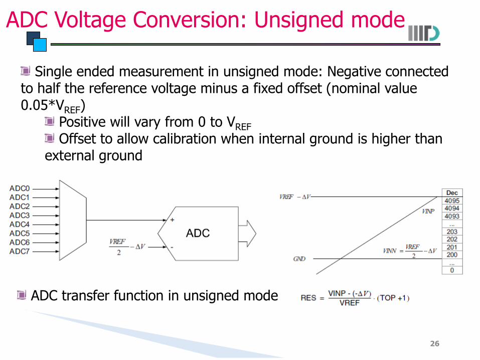
ADC Voltage Conversion: Unsigned mode
Single ended measurement in unsigned mode: Negative connected to half the reference voltage minus a fixed offset (nominal value 0.05*VREF)
Positive will vary from 0 to VREF
Offset to allow calibration when internal ground is higher than external ground
ADC transfer function in unsigned mode

27
xMega: ADC
Compare function: ADC has in-built 12-bit compare function ADC value can be compared with the ADC Compare Register to
generate an interrupt/event if the value is above/below the threshold All 4 ADC channels share the same Compare Register
Starting a conversion: Select the input source for one or more ADC channels ADC conversion started by application software writing to start
conversion bit of the Channel or from any events in the Event System

28
xMega ADC Block Diagram

29
ADC Clock and Conversion Timing
Clocked from Peripheral Clock that can be prescaled to provide ADC Clock
Maximum ADC sampling rate given by ADC clock frequency Propagation delay of ADC measurement given by
RES: Resolution (8- or 12-bit) Greater than one clock cycle but pipelined architecture implies
sampling rate is not limited by propagation delay but by clock frequency

30
ADC Clock and Conversion Timing
MSB of the result is converted first Rest of the bits are converted in the next 3 (for 8-bit resolution) or 5
(12-bit resolution) clock cycles Converting 1 bit takes half a clock cycle During the last clock cycle, result is prepared before the interrupt
flag is set
Single conversion without Gain

31
ADC Clock and Conversion Timing
Single Conversion with Gain
32
ADC Clock and Conversion Timing
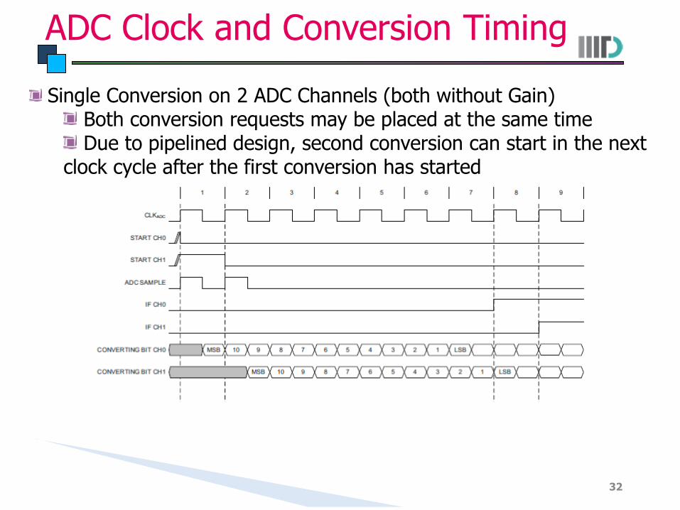
Single Conversion on 2 ADC Channels (both without Gain) Both conversion requests may be placed at the same time Due to pipelined design, second conversion can start in the next
clock cycle after the first conversion has started

33
ADC Clock and Conversion Timing
Single Conversion on 2 ADC Channels (Channel0 with Gain and Channel1 without Gain)

34
ADC Clock and Conversion Timing
Single Conversion on 2 ADC Channels (Channel0 without Gain and Channel1 with Gain)
35
ADC Clock and Conversion Timing
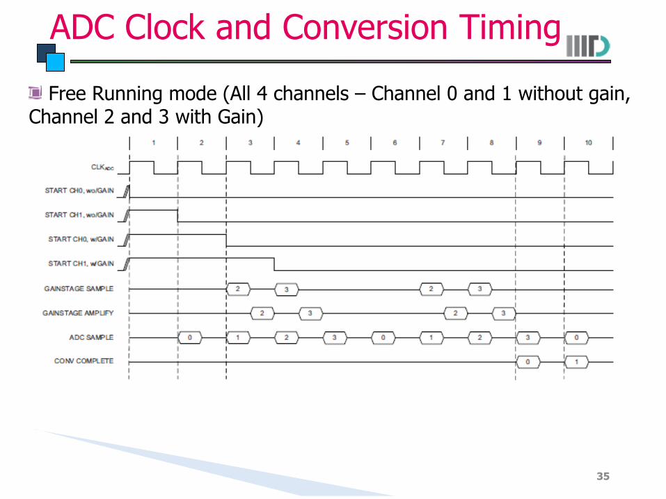
Free Running mode (All 4 channels – Channel 0 and 1 without gain, Channel 2 and 3 with Gain)
What did you learn today?
36
On a small sheet of paper, give me a short (2-3 sentences) description of what you learned today
You can use it to give any broad comments on the class as well


![Universal Serial Bus Microcontroller Seriespdf.eepw.com.cn/e20090826/8915401fb1f67a3d0c4e39cbeb9a3e44.… · • Revised ADC Converter ready bit for ADC Operation-P17,P34,RAS[7]](https://img.dokumen.tips/doc/110x75/5f0fef777e708231d4469ee1/universal-serial-bus-microcontroller-a-revised-adc-converter-ready-bit-for-adc.jpg)


