Embed Size (px)
Citation preview

MIC2593
Dual-Slot PCI Hot Plug Controller
LITTLE FOOT is a registered trademark of Siliconix Incorporated.
Micrel Inc. • 2180 Fortune Drive • San Jose, CA 95131 • USA • tel +1 (408) 944-0800 • fax + 1 (408) 474-1000 • http://www.micrel.com
September 2008 M9999-092208
General Description The MIC2593 is a power controller supporting power distribution requirements for Peripheral Component Interconnect hot plug systems compliant to PCI v2.3 and PCI-X 1.0b. TheMIC2593 provides complete power control support for two PCI slots, including the 3.3VAUX defined by the PCI v2.3 specification. Support for +5V, +3.3V, +12V, and –12V supplies is provided and includes programmable current limit, voltage supervision, fault reporting, and circuit breaker functions which provide fault isolation. The MIC2593 also incorporates an SMBus interface that provides complete status and control of power within each slot. Data sheets and support documentation can be found on Micrel’s web site at: www.micrel.com.
Features
• Supports two completely independent PCI slots: – Compliant to PCI v2.3 and PCI-X 1.0b power
control requirements – Provides all major power control functions for two
independent PCI-X 2.0 slots • Five voltage supplies supported: +12V, -12V,
+5V,+3.3V, and +3.3VAUX – Integrated gate driver circuits, current sense, and
power MOSFETs for 3.3VAUX, +12V, and –12V – High-side +5V and +3.3V gate driver circuits for
external N-Channel MOSFETs • Overcurrent protection with adjustable timeout
eliminates false tripping of circuit breakers • Dual-level, dual-speed overcurrent detection circuitry
for quick fault response without nuisance tripping • Slot power control with “Power-is-Good” and Fault
status reporting – Via software over an SMBus interface or – Via dedicated hardware input/output lines: Hot
Plug Interface (HPI) • Complete thermal isolation between circuitry for Slot A
and Slot B • One General Purpose Input (GPI) pin per slot for
mechanical switch or plug-in card retention/removal input
Applications • PCI hot plug power distribution Ideal Applications: • Mid- and High-end Server Applications compliant to PCI
v2.3, PCI-X 1.0b, and PCI-X 2.0 ___________________________________________________________________________________________________________
Ordering Information
Part Number 5V & 3V Fast-trip Threshold
+12V & –12V Fast-trip Threshold
Operating Temp. Range
Package Lead Finish
MIC2593-2BTQ 100mV 1.5A/0.4A 0° to +70°C 48-Pin TQFP Standard MIC2593-2YTQ 100mV 1.5A/0.4A 0° to +70°C 48-Pin TQFP Pb-Free
Note: Contact factory for availability of the MIC2593-5YTQ option that disables the 100mV fast-trip threshold.

Micrel, Inc. MIC2593
September 2008 2 M9999-092208
Typical Application
PCI Connector
VSTBYB
VSTBYAVAUXA
5VINA
5VSENSEA
3VINA
3VSENSEA
5VINB
5VSENSEB
3VINB
3VSENSEB
5VGATEA
5VOUTA
3VGATEA
3VGATEB
3VOUTB
12VOUTB
12MVOUTB
VAUXB
3VOUTA12VOUTA
12MVOUTA
GND
CFILTERA
A1
A2
A0
ONB
ONA
GPIB
GPIA
AUXENBAUXENA
/INT
SCL
SDA
5VGATEB
5VOUTB
CFILTERB
MIC2593
*R12VGATEA
Si4420DY
Si4420DY
CGATE0.01µF
0.01µF
RSENSE
PCI Bus
3.3VAUXA375mA
3.3V, 7.6A12V, 0.5A–12V, 0.1A
RSENSE
*R12VGATEB
Si4420DY0.01µF
RSENSE
Si4420DY
CGATE
0.01µF
*R3VGATEB
RSENSE
PCI Connector
PCI Bus
3.3VAUXB
3.3V, 7.6A
5V, 5A
* Values for R5VGATE[A/B] and R3VGATE[A/B] may vary depending upon the CGS of the external MOSFETs.** Values determined by design requirements. See “Functional Description” section for detailed information.# MBRS140T3 or equivalent is recommended.Bold lines indicate high current paths
4
11
26
6
7
8
9
12
13
14
16
10
19
31
30
29
28
25
24
23
21
22
–12V, 0.1A20
12V, 0.5A27
2
46
15
*R3VGATEA
0.1µF
0.1µF
0.1µF
0.1µF
0.1µF
0.1µF
0.1µF0.1µF 0.1µF
/FAULTB
/FAULTA1
/INT
SCL
SDA
SMBus I/O ManagementController
48
47
37
43
42
38
35
45
44
VSTBY
**C1 **C2
VSTBY
10k × 3
10k × 4
10k × 2
SDA
SCL
/INT
SMBusBase
Address 39
40
41
GPIB
100k100k
GPIA
VSTBY
12VSLEWA
12VSLEWB
3
34**C3
**C4
36
VSTBY
5 32 17 18
PowerSupply
+12V12V
+5.0V+3.3V
VSTBY
12VINA 12VINB 12MVINA 12MVINB
ONB
ONAAUXENBAUXENA
Hot PlugController
/FAULTB
/FAULTA
GND 33

Micrel, Inc. MIC2593
September 2008 3 M9999-092208
Pin Configuration
12M
VIN
A3V
OU
TAVA
UX
A3V
GAT
EA
3VSE
NSE
A
12M
VIN
B12
MV
OU
TA12
MV
OU
TB
/FAULTACFILTERA12VSLEW
GPI12VINA5VINA
5VSENSEA5VGATEA
5VOUTA12VOUTA
VSTBYA3VINA
3VO
UTB
VAU
XB
3VG
ATE
B3V
SEN
SEB
/FAULTBCFILTERB12VSLEWBGND12VINB5VINB5VSENSEB5VGATEB5VOUTB12VOUTBVSTBYB3VINB
ON
AAU
XEN
AG
ND
SCL
SDA
ON
BAU
XEN
BA0 A1 A2 G
PIB
/INT
Hot-PlugControl
Interface
Slot AInterface
Slot BInterface
48-Pin TQFP (TQ)
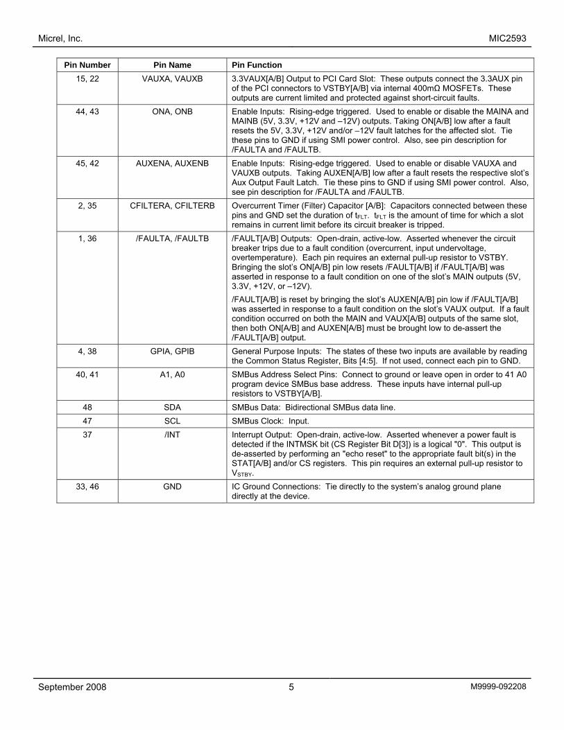
Pin Description Pin Number Pin Name Pin Function
5, 32 12VINA, 12VINB +12V Supply Power [A/B]: Pin 5 is the input to the drain side of the internal MOSFET switch for +12V Slot A. Pin 32 is the input to the drain side of the internal MOSFET switch for +12V Slot B. These two pins must ultimately connect to each other within 10cm of the MIC2593. An undervoltage lockout circuit (UVLO) prevents the switches from turning on while this input is less than its lockout threshold.
10, 27 12VOUTA, 12VOUTB +12V Output [A/B]: Pin 10 is connected to the source terminal of the internal MOSFET switch for +12V Slot A and pin 27 is connected similarly for Slot B.
17, 18 12MVINA, 12MVINB –12V Supply Power [A/B]: Pin 17 is the input to the drain side of the internal MOSFET switch for +12V Slot A. Pin 18 is the input to the drain side of the internal MOSFET switch for –12V Slot B. These two pins must ultimately connect to each other within 10cm of the MIC2593. An undervoltage lockout circuit (UVLO) prevents the switches from turning on while this input is less than its lockout threshold.
19, 20 12MVOUTA, 12MVOUTB –12V Output [A/B]: Pin 19 is connected to the source terminal of the internal MOSFET switch for –12V Slot A and pin 20 is connected similarly for Slot B.
3, 34 12VSLEWA, 12VSLEWB 12V Slew Rate Control [A/B]: Connect capacitors between these pins and ground to set the output slew rates of the +12V and –12V supplies. See the “Functional Description” section for more details.

Micrel, Inc. MIC2593
September 2008 4 M9999-092208
Pin Number Pin Name Pin Function 6, 31 5VINA, 5VINB 5V Supply Power and Sense Input [A/B]: Pin 6 is the (+) Kelvin-sense
connection to the supply side of the sense resistor for 5V Slot A. Pin 31 is the (+) Kelvin sense connection to the supply side of the sense resistor for 5V Slot B. These two pins must ultimately connect to each other within10cm of the MIC2593. An undervoltage lockout circuit (UVLO) prevents the switches from turning on while this input is less than its lockout threshold.
7, 30 5VSENSEA, 5VSENSEB 5V Circuit Breaker Sense Input [A/B]: The current limit thresholds are set by connecting sense resistors between these pins and 5VIN[A/B]. When the current limit threshold of IR = 50mV is reached, the 5VGATE[A/B] pin is modulated to maintain a constant voltage across the sense resistor and therefore a constant current into the load. If the 50mV threshold is exceeded for tFLT (see CFILTER[A/B] pin description), the circuit breaker is tripped and the GATE pin for the affected supply’s external MOSFET is immediately pulled low.
9, 28 5VOUTA, 5VOUTB 5V Power-Good Sense Inputs: Connect to 5V[A/B] outputs. Used to monitor the 5V output voltages for Power-is-Good status.
8, 29 5VGATEA, 5VGATEB 5V Gate Drive Output [A/B]: Each pin connects to the gate of an external N-Channel MOSFET. During power-up, the CGATE and the CGS of the MOSFETs are charged by a 25µA current source. This controls the value of dv/dt seen at the source of the MOSFETs, and hence the current flowing into the load capacitance. During current-limit events, the voltage at the pin is adjusted to maintain constant current through the switch for a period of tFLT. Whenever an overcurrent, thermal shutdown, or input undervoltage fault condition occurs, the GATE pin for the affected slot is immediately brought low. During power-down, these pins are discharged by an internal current source.
12, 25 3VINA, 3VINB 3.3V Supply Power and Sense Input [A/B]: Pin 12 is the (+) Kelvin-sense connection to the supply side of the sense resistor for 3.3V Slot A. Pin 25 is the (+) Kelvin-sense connection to the supply side of the sense resistor for 3.3V Slot B. These two pins must ultimately connect to each other within 10cm of the MIC2593. An undervoltage lockout circuit (UVLO) prevents the switches from turning on while this input is less than its lockout threshold.
13, 24 3VSENSEA, 3VSENSEB 3V Circuit Breaker Sense Input [A/B]: The current limit thresholds are set by connecting sense resistors between these pins and 3VIN[A/B]. When the current limit threshold of IR = 50mV is reached, the 3VGATE[A/B] pin is modulated to maintain a constant voltage across the sense resistor and therefore a constant current into the load. If the 50mV threshold is exceeded for tFLT (see CFILTER[A/B] pin description), the circuit breaker is tripped and the GATE pin for the affected supply’s external MOSFET is immediately pulled low.
16, 21 3VOUTA, 3VOUTB 3.3V Power-Good Sense Inputs: Connect to 3.3V[A/B] outputs. Used to monitor the 3.3V output voltages for Power-is-Good status.
14, 23 3VGATEA, 3VGATEB 3V Gate Drive Output [A/B]: Each pin connects to the gate of an external N-channel MOSFET. During power-up, the CGATE and the CGS of the MOSFETs are connected to a 25µA current source. This controls the value of dv/dt seen at the source of the MOSFETs, and hence the current flowing into the load capacitance. During current limit events, the voltage at this pin is adjusted to maintain constant current through the switch for a period of tFLT. Whenever an overcurrent, thermal shutdown, or input undervoltage fault condition occurs, the GATE pin for the affected slot is immediately brought low. During power down, these pins are discharged by an internal current source.
11, 26 VSTBYA, VSTBYB .3V Standby Input Voltage: Required to support PCI VAUX output. Additionally, the SMBus logic and internal registers run off of VSTBY[A/B] to ensure that the MIC2593 is accessible during standby modes. A UVLO circuit prevents turn-on of this supply until VSTBY[A/B] rises above its UVLO threshold. Both pins must be connected together externally at the IC.
Micrel, Inc. MIC2593
September 2008 5 M9999-092208
Pin Number Pin Name Pin Function 15, 22 VAUXA, VAUXB 3.3VAUX[A/B] Output to PCI Card Slot: These outputs connect the 3.3AUX pin
of the PCI connectors to VSTBY[A/B] via internal 400mΩ MOSFETs. These outputs are current limited and protected against short-circuit faults.
44, 43 ONA, ONB Enable Inputs: Rising-edge triggered. Used to enable or disable the MAINA and MAINB (5V, 3.3V, +12V and –12V) outputs. Taking ON[A/B] low after a fault resets the 5V, 3.3V, +12V and/or –12V fault latches for the affected slot. Tie these pins to GND if using SMI power control. Also, see pin description for /FAULTA and /FAULTB.
45, 42 AUXENA, AUXENB Enable Inputs: Rising-edge triggered. Used to enable or disable VAUXA and VAUXB outputs. Taking AUXEN[A/B] low after a fault resets the respective slot’s Aux Output Fault Latch. Tie these pins to GND if using SMI power control. Also, see pin description for /FAULTA and /FAULTB.
2, 35 CFILTERA, CFILTERB Overcurrent Timer (Filter) Capacitor [A/B]: Capacitors connected between these pins and GND set the duration of tFLT. tFLT is the amount of time for which a slot remains in current limit before its circuit breaker is tripped.
1, 36 /FAULTA, /FAULTB /FAULT[A/B] Outputs: Open-drain, active-low. Asserted whenever the circuit breaker trips due to a fault condition (overcurrent, input undervoltage, overtemperature). Each pin requires an external pull-up resistor to VSTBY. Bringing the slot’s ON[A/B] pin low resets /FAULT[A/B] if /FAULT[A/B] was asserted in response to a fault condition on one of the slot’s MAIN outputs (5V, 3.3V, +12V, or –12V). /FAULT[A/B] is reset by bringing the slot’s AUXEN[A/B] pin low if /FAULT[A/B] was asserted in response to a fault condition on the slot’s VAUX output. If a fault condition occurred on both the MAIN and VAUX[A/B] outputs of the same slot, then both ON[A/B] and AUXEN[A/B] must be brought low to de-assert the /FAULT[A/B] output.
4, 38 GPIA, GPIB General Purpose Inputs: The states of these two inputs are available by reading the Common Status Register, Bits [4:5]. If not used, connect each pin to GND.
40, 41 A1, A0 SMBus Address Select Pins: Connect to ground or leave open in order to 41 A0 program device SMBus base address. These inputs have internal pull-up resistors to VSTBY[A/B].
48 SDA SMBus Data: Bidirectional SMBus data line. 47 SCL SMBus Clock: Input. 37 /INT Interrupt Output: Open-drain, active-low. Asserted whenever a power fault is
detected if the INTMSK bit (CS Register Bit D[3]) is a logical "0". This output is de-asserted by performing an "echo reset" to the appropriate fault bit(s) in the STAT[A/B] and/or CS registers. This pin requires an external pull-up resistor to VSTBY.
33, 46 GND IC Ground Connections: Tie directly to the system’s analog ground plane directly at the device.

Micrel, Inc. MIC2593
September 2008 6 M9999-092208
Absolute Maximum Ratings(1)
Supply Voltage (12VIN) ..........................................................................+14V (12MVIN) .......................................................................–14V (5VIN) ..............................................................................+7V (3VIN), (VSTBY) .................................................................+7V Any Logic Pin ....................................................–0.5 to 3.6V Output Current (FAILT[A/B], /INT, SDA). ....................10mA Lead Temperature IR Reflow, Peak Temperature........................ 240 0°C/–5°C Storage Temperature (Ts) .........................–65°C to +150°C ESD Rating(3)
Human Body Model........................................................2kV Machine Model .............................................................200V
Operating Ratings(2)
Supply Voltage (12VIN) .................................................... +11.65V to +12.6V (12MVIN) ................................................... –11.0V to –13.2V (5VIN) .......................................................... +4.85V to 5.25V (3VIN) ............................................................ +3.1V to +3.6V (VSTBY) .......................................................... +3.15V to 3.6V Ambient Temperature (TA) .............................. 0°C to +70°C Junction Temperature (TJ) ......................................... 125°C Thermal Resistance TQFP (θJA) ......................................................56.5°C/W
Electrical Characteristics(4) 12VIN[A/B] = 12V; 12MVIN[A/B] = –12V; 5VIN[A/B] = 5V; 3VIN[A/B] = 3.3V; VSTBY[A/B] = 3.3V; TA = 25°C; unless otherwise noted. Bold indicates specification applies over the full operating rating temperature range from 0°C to 70°C.
Symbol Parameter Condition Min Typ Max Units ICC12V ICC5V ICC3.3V ICC12MV ICCVSBY
Supply Current 0.6 1.2 0.5 –1.0 2.5
2.0 2.0 0.7 –2.0 5.0
mA mA mA mA mA
VUVLO(12V)
VUVLO(3V)
VUVLO(5V)
VUVLO(12MV) VUVLO(STBY)
Under Voltage Lockout Thresholds 12VIN[A/B] 3VIN[A/B] 5VIN[A/B] 12MVIN[A/B] VSTBY[A/B]
12VIN increasing 3VIN increasing 5VIN increasing 12MVIN increasing VSTBY increasing
8
2.2 3.7 –10 2.8
9
2.5 4.0 –9 2.9
10
2.75 4.3 –8 3.0
V V V V V
VHYSUV Under Voltage Lockout Hysteresis - 12VIN, 12MVIN, 5VIN, 3VIN
180 mV
VHYSSTBY Under-voltage Lockout Hysteresis - VSTBY
50 mV
VUVTH(12V)
VUVTH(12MV)
VUVTH(3V)
VUVTH(5V) VUVTH(VAUX)
Power Good Under-Voltage Thresholds 12VOUT[A/B] 12MVOUT [A/B] 3VOUT [A/B] 5VOUT [A/B] VAUX[A/B]
12VOUT[A/B] decreasing 12MVOUT[A/B] decreasing 3VOUT[A/B] decreasing 5VOUT[A/B] decreasing VAUX[A/B] decreasing
10.2
–10.8 2.7 4.4 2.7
10.5
–10.6 2.8 4.5 2.8
10.8
–10.2 2.9 4.7 2.9
V V V V V
VHYSPG Power-Good Detect Hysteresis 30 mV VGATE 5VGATE/3VGATE Voltage 12VIN–15 12VIN V IGATE(SOURCE) 5VGATE/3VGATE Charge Current start cycle 15 25 35 µA IGATE(SINK) 5VGATE/3VGATE Sink Current (Fault Off) any fault condition, VGATE = 5V 70 mA

Micrel, Inc. MIC2593
September 2008 7 M9999-092208
Symbol Parameter Condition Min Typ Max Units VFILTER CFILTER Threshold Voltage 1.20 1.25 1.30 V IFILTER CFILTER [A/B] Charge Current V5VIN[A/B] – V5SENSE[A/B] > VTHILIMIT
and/or V3VIN[A/B] – V3SENSE[A/B] > VTHILIMIT
1.80 2.5 5.0 µA
ISLEW 12VSLEW[A/B] Charge Current During turn-on only 13 22 35 µA VTHILIMIT Current Limit Threshold Voltages
5V[A/B] Supplies 3.3V[A/B] Supplies
V5VIN[A/B] – V5VSENSE[A/B] V3VIN[A/B] – V3VSENSE[A/B]
35 35
50 50
65 65
mV mV
VTHFAST Fast-Trip Current Limit Thresholds 5V[A/B] and 3V[A/B]
MIC2593-2xTQ
90
113
135
mV
I5VSENSE[A/B] 5VSENSE[A/B] Input Current V5VIN[A/B] – V5VSENSE[A/B] = 50mV(5) 0.5 µA I3VSENSE[A/B] 3VSENSE[A/B] Input Current V3VIN[A/B] – V3VSENSE[A/B] = 50mV(5) 0.5 µA VIL LOW-Level Input Voltage
ON[A/B], AUXEN[A/B], GPI[A/B], SCL, SDA, A[0-2]
0.8 V
VOL Output LOW Voltage /FAULT[A/B], /INT, SDA
IOL = 3mA 0.4 V
VIH HIGH-Level Input Voltage ON[A/B], AUXEN[A/B], GPI[A/B], SCL, SDA, A[0-2]
2.1 V
RPULL-UP Internal Pullups from A[0-2] to VSTBY 40 kΩ ILKG,OFF(12VIN[A/B]) 12VIN[A/B] Input Leakage Current VSTBY[A/B] = +3.3V
12VIN[A/B] = OFF(5) 1 µA
ILKG,OFF(12MVIN[A/B]) 12MVIN[A/B] Input Leakage Current VSTBY[A/B] = +3.3V 12MVIN[A/B] = OFF(5)
60 µA
ILKG,OFF(5VIN[A/B]) 5VIN[A/B] Input Leakage Current VSTBY[A/B] = +3.3V 5VIN[A/B] = OFF(5)
200 µA
ILKG,OFF(3VIN[A/B]) 3VIN[A/B] Input Leakage Current VSTBY[A/B] = +3.3V 3VIN[A/B] = OFF(5)
1 µA
IIL Input Leakage Current SCL, ON[A/B], AUXEN[A/B], GP[A/B])
±5 µA
ILKG(OFF) Off-State Leakage Current SDA, /FAULT[A/B], /INT
±5 µA
Overtemperature Shutdown & Reset Thresholds, with overcurrent on slot
TJ Increasing, each slot (6) TJ Decreasing, each slot (6)
140 130
°C °C
TOV
Overtemperature Shutdown & Reset Thresholds, all other conditions (all outputs will latch OFF)
TJ Increasing, both slots (6) TJ Decreasing, both slots (6)
160 150
°C °C
ROUT(12V) ROUT(12MV) ROUT(AUX)
Output MOSFET Resistance +12V MOSFET –12V MOSFET VAUX MOSFET
IDS = 500mA, TJ = 125°C IDS = 100mA, TJ = 125°C IDS = 375mA, TJ = 125°C
500 2
400
mΩ Ω
mΩ

Micrel, Inc. MIC2593
September 2008 8 M9999-092208
Symbol Parameter Condition Min Typ Max Units VOFF(+12V) VOFF(12MV) VOFF(AUX)
Off-State Output Offset Voltage 12VOUT[A/B] 12MVOUT[A/B] VAUX[A/B]
12VOUT[A/B] = Off, TJ = 125°C 12MVOUT[A/B] = Off, TJ = 125°C VAUX[A/B] = Off, TJ = 125°C
–50
50
50
mV mV mV
ILIM(12V) ILIM(12MV)
Current Limit Slow-Trip Threshold +12V MOSFET –12V MOSFET
12VOUT[A/B] = 0V 12MVOUT[A/B] = 0V
0.52
–0.11
1.0
–0.2
1.5
–0.3
A A
IFASTLIM(12V) IFASTLIM(12MV)
Current Limit Fast-Trip Thresholds +12V MOSFET –12V MOSFET
MIC2593-2BTQ 12VOUT[A/B] 12MVOUT[A/B]
1.0 –0.20
2.15 –0.45
3.0 –0.6
A A
IAUX(THRESH) Auxiliary Output Current Limit Threshold Figure 4
Current which must be drawn from VAUX to register as a fault
0.84 A
ISC(TRAN) Maximum Transient Short Circuit Current
VAUX Enabled, then Grounded IMAX = VSTBY / RDS(AUX) A
ILIM(AUX) Regulated Current after Transient From end of ISC(TRAN) to CFILTER Time Out
0.375 0.7 1.35 A
RDISCH RDISCH(12V) RDISCH(12MV) RDISCH(3V) RDISCH(5V) RDISCH(VAUX)
Output Discharge Resistance 12VOUT[A/B] 12MVOUT[A/B] 3VOUT[A/B] 5VOUT[A/B] VAUX[A/B]
12VOUT[A/B] = 6.0V 12MVOUT[A/B] = –6.0V 3VOUT[A/B] = 1.65V 5MVOUT[A/B] = 2.5V 5VOUT[A/B] = 1.65V
1600 600 150 150 430
Ω Ω Ω Ω Ω
tOFF(3V) tOFF(5V)
Current Limit Response Time for 3.3V and 5V Outputs, Figure 2
MIC2593-2 CGATE = 10nF VIN – VSENSE = 200mV
1 µs
TSC(TRAN) VAUX Current Limiter Response Time, Figure 5
VAUX[A/B] = 0V (6) 33 µs
tOFF(12V) 12V Current Limit Response Time, Figure 3
12VOUT[A/B] = 0V (6) 1 µs
tOFF(12MV) –12V Current Limit Response Time, Figure 3
12MVOUT[A/B] = 0V (6) 1 µs
tPROP(3VFAULT) Delay from 3V[A/B] overcurrent-limit to FAULT Output
MIC2593-2 VSENSE – VTHLIMIT = 200mV CFILTER = open
1 µs
tPROP(5VFAULT) Delay from 5V[A/B] overcurrent-limit to FAULT Output
MIC2593-2 VSENSE – VTHLIMIT = 200mV CFILTER = open
1 µs
tW ON[A/B], AUXEN[A/B] Pulse Width Note 5 100 ns tPOR MIC2593 Power-On Reset Time after
VSTBY becomes valid Note 5 500 µs
SMBus Timing, Note 5 t1 SCL (Clock) Period Figure 1 2.5 µs t2 Data In Set-Up Time to SCL HIGH Figure 1 100 ns
Micrel, Inc. MIC2593
September 2008 9 M9999-092208
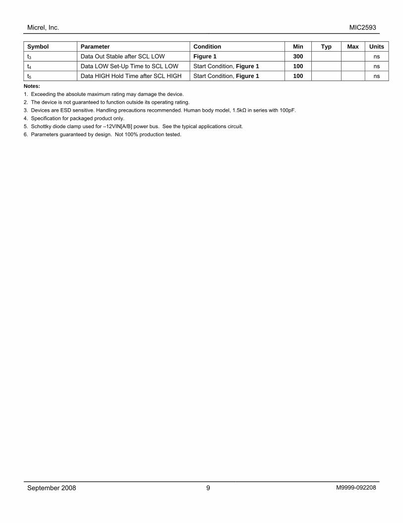
Symbol Parameter Condition Min Typ Max Units t3 Data Out Stable after SCL LOW Figure 1 300 ns t4 Data LOW Set-Up Time to SCL LOW Start Condition, Figure 1 100 ns t5 Data HIGH Hold Time after SCL HIGH Start Condition, Figure 1 100 ns
Notes: 1. Exceeding the absolute maximum rating may damage the device. 2. The device is not guaranteed to function outside its operating rating. 3. Devices are ESD sensitive. Handling precautions recommended. Human body model, 1.5kΩ in series with 100pF. 4. Specification for packaged product only. 5. Schottky diode clamp used for –12VIN[A/B] power bus. See the typical applications circuit. 6. Parameters guaranteed by design. Not 100% production tested.

Micrel, Inc. MIC2593
September 2008 10 M9999-092208
Test Circuit t1
SCL
SDAData In
SDAData Out
t4 t2
t3
t5
Figure 1. SMBus Timing
6V12VGATE
VTHFAST
VTHILIMIT
tOFF(12V)
1V3VGATE
VTHFAST
VTHLIMIT
tOFF3
Figure 2. 12V Current Limit Response Timing Figure 3. 3V Current Limit Response Timing
0 Amps
IOUT(AUX) IOUT(AUX)
ILIM(AUX)
Must Trip
May Not Trip
IAUX(THRESH)
0 Amps
IOUT(AUX)
tSC(TRAN)
ILIM(AUX)
ISC(TRAN)
Figure 4. VAUX Current Limit Threshold Figure 5. VAUX Current Limit Response Timing

Micrel, Inc. MIC2593
September 2008 11 M9999-092208
Functional Description Hot Swap Insertion When circuit boards are inserted into systems carrying live supply voltages (“hot-plugged”), high inrush currents often result due to the charging of bulk capacitance that resides across the circuit board’s supply pins. This transient inrush current can cause the system’s supply voltages to temporarily go out of regulation, causing data loss or system lock-up. In more extreme cases, the transients occurring during a hot plug event may cause permanent damage to connectors or on-board components. The MIC2593 addresses these issues by limiting the inrush currents to the load (PCI Board), and thereby controlling the rate at which the load’s circuits turn-on. In addition to this inrush current control, the MIC2593 offers input and output voltage supervisory functions and current limiting to provide robust protection for both the system and circuit board.
System Interfaces The MIC2593 employs two system interfaces: the hardware Hot Plug Interface (HPI) and the System Management Interface (SMI). The HPI includes ON[A/B], AUXEN[A/B], as well as /FAULT[A/B]; the SMI consists of SDA, SCL, and /INT, whose signals conform to the levels and timing of the SMBus specification. The MIC2593 can be operated exclusively from the SMI, or can employ the HPl for power control while continuing to use the SMI for access to all but the power control registers. In addition to the basic power control features of the MIC2593 accessible by the HPI, the SMI also gives the host access to the following information from the part:
1. Fault conditions occurring on each supply. 2. GPI[A/B] pin status.
When using the System Management Interface for power control, do not use the Hot Plug Interface. Conversely, when using the Hot Plug Interface for power control, do not execute power control commands over the System Management Interface bus (all other register accesses via the SMI bus remain permissible while in the HPI control mode). When utilizing the SMI exclusively, the HPI input pins ON[A/B] and AUXEN[A/B] should be tied to ground as shown below in Figure 6 (Disabling HPI when SMI control is used). This configuration safeguards the power slots in the event that the SMBus communication link is disconnected for any reason. Additionally, when utilizing the HPI exclusively, the SMBus (or SMI) will be inactive if the input pins (SDA, SCL, A0, A1, and A2) are configured as shown in Figure 6 below (disabling SMI when HPI Control is used).
Power-On Reset and Power Cycling The MIC2593 utilizes VSTBY[A/B] as the main supply input source. VTSBY[A/B] is required for proper operation of the MIC2593 SMBus interface and registers and must be applied at all times. A Power-On Reset (POR) cycle is initiated after VSTBY[A/B] rises above its UVLO threshold and remains valid at that voltage for 500µs. All internal registers are cleared after POR. If VSTBY[A/B] is recycled, the MIC2593 enters a new power-on reset cycle. VSTBY[A/B] must be the first supply input applied followed by the MAIN supply inputs of 12VIN, 12MVIN, 5VIN, and 3VIN. The MAIN supply inputs may be applied in any order. The SMBus is ready for access at the end of the POR interval (500µs after VSTBY[A/B] is valid). All outputs remain off during tPOR.
MIC2593
A2/INTSDASCL
A0
VSTBY
A1
100k47
48
37
39
40
41
100k
Disabling SMI whenHPI Control is used
Disabling HPI whenSMI Control is used
100k
/INT AUXENAAUXENBONAONB
MIC2593
45
42
44
43
Figure 6. Input Pin Configuration for Disabling HPI/SMI Control

Micrel, Inc. MIC2593
September 2008 12 M9999-092208
Power-Up Cycle When a slot is off, the 5VGATE and 3VGATE pins are held low with an internal pull-down current source. When a slot’s MAIN outputs are enabled by applying a rising-edge signal at the ON[A/B] control input and all input voltages are above their respective undervoltage lockout thresholds, all four main supplies will then execute a controlled turn on. The 5VGATE and 3VGATE pins are each connected to a constant current source of 25µA, nominal. Both the 5V and 3.3V outputs act as source followers, where: [ ]TH(ON)GATESOURCE VVV −=
until the associated output is equal to its input. The voltages on the gates of the external MOSFETs for the 5V and 3.3V MAIN supplies will continue to rise to approximately 11.5V, ensuring minimum RDS(ON) of the MOSFET. Note that a delay exists between the ON command to a slot and the appearance of voltage at the slot’s 3.3V or 5V MAIN output. This delay is the time required to charge the 3V or 5V GATE output up to the threshold voltage of the external MOSFET (typically about 4V). For the 5V and 3.3V MAIN supplies, the source (output) side of the external MOSFET will reach the drain (input) voltage in a time given by:
( )
E)GATE(SOURC
DRAINGATEDELAY I
VCt
×=
Table 1 provides a reference list of the expected GATE output slew rate for the 3.3V and 5V supplies using several (decade-scale) standard capacitors.
ISLEW = 25µA CGATE dv/dt (load)
0.001µF 25000V/s 0.01µF 2500V/s 0.1µF 250V/s 1µF 25V/s
Table 1. 3.3V/5V Output Slew Rate Selection
For the +12V and –12V supplies, the output slew rate is controlled by capacitors connected to the 12VSLEWA and 12VSLEWB pins. To determine the minimum value of the slew rate capacitor, (CSLEW), and to ensure the device does not enter into current limit during start-up, the following equation is used:
LOADMV]LIM[12V/12
SLEWSLEW C
II
(min)C ×=
where CLOAD is the load capacitance connected to the +12V and –12V outputs, ILIM[12V/12MV] are the current limit slow-trip thresholds and ISLEW is the slew rate charge current found in the “Electrical Characteristics” table. The slew rate dv/dt is computed by:
6
SLEW
SLEW
10CI
load) (at dv/dt×
=
By appropriately selecting the value of CSLEW, the magnitude of the inrush current will not exceed the current limit for a given load capacitance. Since one capacitor fixes the slew rate for both +12V and –12V, the capacitor value should be chosen to provide the slower slew rate of the two. Table 2 depicts the ±12V output slew rate for various values of CSLEW.
ISLEW = 22µA CGATE dv/dt (load)
0.001µF 22V/ms 0.01µF 2.2V/ms 0.1µF 0.22V/ms 1µF 0.022V/ms
Table 2. ±12V Output Slew Rate Selection
Power Down Cycle When a slot is turned off, internal switches are connected to each of the outputs to discharge the PCI board's bypass capacitors to ground.
Standby Mode Standby mode is entered when any (one or more) enabled MAIN supply input (12VIN, 12MVIN, 5VIN and/or 3VIN) drops below its respective UVLO threshold. The MIC2593 supplies two 3.3V auxiliary outputs, VAUX[A/B], satisfying PCI 2.x specifications. These outputs are fed via the VSTBY[A/B] input and controlled by the AUXEN[A/B] inputs or via their SMI bus Control Registers. These outputs are independent of the MAIN outputs: should one or more of the MAIN supply inputs move below its UVLO thresholds, VAUX[A/B] will still function as long as VSTBY[A/B] is present. Prior to entering standby mode, ONA and ONB (or the MAINA and MAINB bits in the Control Registers) inputs should be de-asserted. If this is not done, the MIC2593 will assert /FAULT and also /INT if interrupts are enabled, when the MIC2593 detects an undervoltage condition on a supply input.
Circuit Breaker Functions The MIC2593 provides an electronic circuit breaker function that protects against excessive loads, such as short circuits, at each supply. When the current from one or more of a slot’s MAIN outputs exceeds the current limit threshold (50mV/RSENSE for 3.3V and 5V, 1.0A for +12V, and/or 0.2A for –12V) for a duration greater than the overcurrent timer, tFLT, the circuit breaker is tripped and all MAIN supplies (all outputs except VAUX[A/B]) are shut off. Should the load current exceed ITHFAST (+12V and –12V), or cause a MAIN output’s VSENSE to exceed VTHFAST (+3.3V and +5V), the outputs are shut off with no delay. Undervoltage conditions on the MAIN supply inputs also

Micrel, Inc. MIC2593
September 2008 13 M9999-092208
trip the circuit breaker, but only when the MAIN outputs are enabled (to signal a supply input brown-out condition). The VAUX[A/B] outputs have their own separate circuit breaker functions. VAUX[A/B] do not incorporate a fast-trip threshold, but instead regulate the output current into a fault to avoid exceeding their operating current limit. The circuit breaker will trip due to overcurrents on VAUX[A/B] when the overcurrent fault timer (tFLT) expires. This use of the overcurrent timer prevents the circuit breaker from tripping prematurely due to brief current transients. Following a fault condition, the outputs can be turned on again via the ON inputs (if the fault occurred on one of the MAIN outputs), via the AUXEN inputs (if the fault occurred on the AUX outputs), or by cycling both ON and AUXEN (if faults occurred on both the MAIN and AUX outputs). A fault condition can alternatively be cleared under SMI control of the ENABLE bits in the CNTRL[A/B] registers (See Register Bits D[1:0]). When the circuit breaker trips, /FAULT[A/B] will be asserted if the outputs were enabled through the Hot Plug Interface inputs. At the same time, /INT will be asserted (unless interrupts are masked). Note that /INT is de-asserted by writing a Logic 1 back into the respective fault bit position(s) in the STAT[A/B] register or the Common Status Register. The response time (tFLT) of the MIC2593’s primary overcurrent detector is set by external capacitors at the CFILTER[A/B] pins to GND. For Slot A, CFILTER[A] is located at Pin 2; for Slot B, CFILTER[B] is located at Pin 35. For a given response time, the value for CFILTER[A/B] is given by.
3FILTER
FILTERFLT[A/B]
10(V)V
)(I(ms)tF)B](CFILTER[A/
×
×=
Aμμ
where tFLT[A/B] is the selected overcurrent response time and IFILTER and VFILTER are specified in the “Electrical Characteristics” table.
Thermal Shutdown The internal +12V, –12V, and VAUX MOSFETs are protected against damage not only by current limiting, but by dual-mode overtemperature protection as well. Each slot controller on the MIC2593 is thermally isolated from the other. Should an overcurrent condition raise the junction temperature of one slot’s controller and internal pass elements to 140°C, all of the outputs for that slot (including VAUX) will be shut off, and the slot’s /FAULT output will be asserted. The other slot’s operation will remain unaffected. However, should the MIC2593’s overall die temperature exceed 160°C, both slots (all outputs, including VAUXA and VAUXB) will be shut off, whether or not a current limit condition exists. A 160°C overtemperature condition additionally sets the overtemperature bit (OT_INT) in the Common Status Register.
Output Power-Good Status For the MIC2593, “Power-is-Good” is valid on a slot when the outputs of the four MAIN supplies (12V, –12V, 5V, and 3.3V) and the auxiliary supply output are all above their respective power-good thresholds specified in the “Electrical Characteristics” table. The power-good status of either slot is verified by polling the CNTRL[A/B] Register Bits D[7:6]. CNTRL[A/B] Register Bits D[7] and D[6] indicate output power-good status for the AUX supply and MAIN supplies, respectively. Figure7 below illustrates an equivalent logic circuit that determines the output power-good status for the MAIN and AUX supplies.
MAIN[A/B]PG(3)
3VAUX_UV[A/B](1)
12VOUT_UV[A/B](1)
3VOUT_UV[A/B](1)
AUX[A/B]PG(2)
VSTBY[A/B]
VSTBY[A/B]
Notes: 1. Internal flag 2. CNTRL[A/B] Register Bit D[7] 3. CNTRL[A/B] Register Bit D[6]
Figure 7. Power-Good Status Logic Diagram

Micrel, Inc. MIC2593
September 2008 14 M9999-092208
General Purpose Input (GPI) Pins Two pins on the MIC2593 are available for use as GPI pins. The logic state of each of these pins can be determined by polling Bits [4:5] of Common Status Register. Both of these inputs are compliant to 3.3V. If unused, connect the GPI[A/B] pins to GND.
Fault Reporting and /INT Interrupt Generation
SMI-only Control Applications In applications where the MIC2593 is controlled only by the SMI, the ON[A/B] and AUXEN[A/B] should be connected to GND as shown in Figure 6. In this case, the MIC2593’s /FAULT[A/B] outputs and STAT[A/B] Register Bit D[7] (FAULT[A/B]) are not activated, as fault status is determined by polling STAT[A/B] Register Bits D[4:0] and CS (Common Status) Register Bits D[2:1]. Individual fault bits in STAT[A/B] and CS are asserted after power-on-reset when Either or both CNTRL[A/B] Register Bits D[1:0] are asserted, AND
• 12VIN[A/B], 12MVIN[A/B], 5VIN[A/B], 3VIN[A/B], or VSTBY[A/B] input voltage is lower than its respective ULVO threshold, OR
• The fast OC circuit breaker[A/B] has tripped, OR • The slow OC circuit breaker[A/B] has tripped
AND its filter timeout has expired, OR
• The slow OC circuit breaker[A/B] has tripped AND Slot[A/B] die temperature exceeds 140°C, OR
• The MIC2593’s global die temperature exceeds 160°C
To clear any one or all STAT[A/B] Register Bits D[4:0] and/or CS Register Bits D[2:1] once asserted, a software subroutine can perform an “echo reset” where a Logical “1” is written back to those register bit locations that have indicated a fault. The open-drain, active-LOW /INT output signal is activated after power-on-reset when the INTMSK bit (CS Register Bit D[3]) has been reset to Logical “0”. Once activated, the /INT output is asserted by any one of the fault conditions listed above and de-asserted when one or all STAT[A/B] Register Bits D[4:0] and/or CS Register Bits D[2:1] are reset upon the execution of an SMBus “echo reset” WRITE_BYTE cycle.
HPI-only Control Applications In applications where the MIC2593 is controlled only by the HPI, SMBus signals SCL, SDA, and /INT signals are connected to VSTBY as shown in Figure 6. In this configuration, the MIC2593’s /FAULT[A/B] outputs are activated after power-on-reset and become asserted when:
/INT*
/FAULT_[A/B]
IMAIN_OUT[A/B]
MAIN_OUT[A/B]
IAUX_OUT[A/B]
AUX_OUT[A/B]
AUXEN[A/B]0
VIH VIHVIL
VIH
ILIM(AUX)
ISTEADY-STATE
ILIM(MAIN)
ISTEADY-STATE
ON[A/B]0
0
0
0
0
0
0
VIH
VIL
+3.3V
tPOR
VSTBY
UVLO
tFLT
tFLT
* *
* /INT de-asserted by software
Figure 8. Hot Plug Interface Mode Operation

Micrel, Inc. MIC2593
September 2008 15 M9999-092208
Either or both external ON[A/B] and AUXEN[A/B] input signals are asserted, AND
• 12VIN[A/B], 12MVIN[A/B], 5VIN[A/B], 3VIN[A/B], or VSTBY[A/B] input voltage is lower than its respective ULVO threshold, OR
• The fast OC circuit breaker[A/B] has tripped, OR • The slow OC circuit breaker[A/B] has tripped
AND its filter timeout[A/B] has expired, OR • The slow OC circuit breaker[A/B] has tripped
AND Slot[A/B] die temperature exceeds 140°C, OR
• The MIC2593’s global die temperature exceeds160°C
In order to clear /FAULT[A/B] outputs once asserted, ON[A/B] and/or AUXEN[A/B] input signals must be de-asserted. Please see the /FAULT[A/B] pin description for additional information.
Hot Plug Interface (HPI) Operation Once the input supplies are above their respective UVLO thresholds, the Hot Plug Interface can be utilized for power control by enabling the control input pins (AUXEN[A/B] and ON[A/B]) for each slot. In order for the MIC2593 to switch on the VAUX supply for either slot, the AUXEN[A/B] control must be enabled after the power-on-reset delay, tPOR (typically 500µs), has elapsed. The MAIN output supplies can also be enabled after tPOR. The timing response diagram of Figure 8 illustrates a Hot Plug Interface operation where an overcurrent fault is detected by the MIC2593 controller after initiating a power-up sequence. The figure illustrates the output response of /FAULT, /INT, VAUX[A/B] supplies, and an external MOSFET control MAIN[A/B] output supply, either 3.3V or 5V.
MIC2593 SMBus Address Configuration The MIC2593 responds to its own unique address which is assigned using A2, A1, and A0. These represent the 3 LSBs of its 7-bit address, as shown in Table 3. These address bits are assigned only during power up of the VSTBY[A/B] supply input. These three bits allow up to eight MIC2593 devices in a single system. These pins are either grounded or left unconnected to specify a logical 0 or 1, respectively. A pin designated as a logical 1 may also be pulled up to VSTBY.
Serial Port Operation The MIC2593 uses standard SMBus Write_Byte and Read_Byte operations for communication with its host. The SMBus Write_Byte operation involves sending the device’s slave address, with the R/W bit (LSB) set to the low (write) state, followed by a command byte and a data byte. The SMBus Read_Byte operation is similar, but is a composite write and read operation: the host first sends the device’s slave address followed by the command byte, as in a write operation. A new “Start” bit must then be sent to the MIC2593, followed by a repeat of the slave address with the R/W bit set to the high (read) state. The data to be read from the part may then be clocked out. There is one exception to this rule: If the location latched in the pointer register from the last write operation is known to be correct (i.e., points to the desired register within the MIC2593), then the “Receive_Byte” procedure may be used. To perform a Receive_Byte operation, the host sends an address byte to select the slave MIC2593, with the R/W bit set to the high (read) state, and then retrieves the data byte. Figures 9 through 11 show the formats for these data read and data write procedures. The Command Register is eight bits (one byte) wide. This byte carries the address of the MIC2593’s register to be operated upon. The command byte values corresponding to the various MIC2593 register addresses are shown in Table 4. Command byte values other than 0000 0XXXb = 00h - 07hare reserved and should not be used.
Inputs MIC2593 Slave Addresses A2 A1 A0 Binary Hex 0 0 0 1000 000b 80h 0 0 1 1000 001b 82h 0 1 0 1000 010b 84h 0 1 1 1000 011b 86h 1 0 0 1000 100b 88h 1 0 1 1000 101b 8Ah 1 1 0 1000 110b 8Ch 1 1 1 1000 111b 8Eh
Table 3. MIC2593 SMBus Addressing

Micrel, Inc. MIC2593
September 2008 16 M9999-092208
Register Set and Programmer’s Model Target Register Common
Byte Value Label Description Read Write
Power-On Default
RESERVED Do not Use 00h n/a n/a RESERVED Do not Use 01h n/a n/a CNTRLA Control Register Slot A 02h 02h 00h CNTRLB Control Register Slot B 03h 03h 00h STATA Slot A Status 04h 04h 00h STATB Slot B Status 05h 05h 00h CS Common Status Register 06h 06h Xxxx 0000b RESERVED Reserved / Do not Use 07h 0FFh 07h 0FFh Undifined
Table 4. MIC2593 Register Addresses
S 1 0 0 1 0 A 0 0 0 0 0 0 X X A A P
MIC2593 Slave Address
DATA
CLK
Command Byte to MIC2593 Data Byte to MIC2593
START STOPR/W = WRITE ACKNOWLEDGE ACKNOWLEDGE ACKNOWLEDGE
Master to slave transfer,i.e., DATA driven by master.
Slave to master transfer,i.e., DATA driven by slave.
Figure 9.WRITE_BYTE Protocol
S 1 0 0 1 A2 A1 A0 A2 A1 A00 A 0 0 0 0 0 0 X X A S 1 1 10 0 A /A P
MIC2593 Slave Address
DATA
CLK
Command Byte to MIC2593 MIC2593 Slave Address Data Read From MIC2593
START START STOPR/W = WRITE R/W = READACKNOWLEDGE ACKNOWLEDGE ACKNOWLEDGE NOT ACKNOWLEDGE
Master to slave transfer,i.e., DATA driven by master.
Slave to master transfer,i.e., DATA driven by slave.
Figure 10.READ_BYTE Protocol
S 1 0 0 1 1 A /A P
MIC2593 Slave Address
DATA
CLK
Byte Read from MIC2593
START STOPR/W = READ ACKNOWLEDGE NOT ACKNOWLEDGE
Master to slave transfer,i.e., DATA driven by master.
Slave to master transfer,i.e., DATA driven by slave.
Figure 11.RECEIVE_BYTE Protocol

Micrel, Inc. MIC2593
September 2008 17 M9999-092208
Detailed Register Descriptions below: Control Register, Slot A (CNTRLA) 8-Bits, Read/Write
Control Register, Slot A (CNTRLA) D[7] D[6] D[5] D[4] D[3] D[2] D[1] D[0]
read-only read-only read-only read-only read-only read-only read/write read/write AUXAPG MAINAPG Reserved Reserved Reserved Reserved MAINA AUXA
Bit(s) Function Operation
AUXAPG AUX output power-good status, Slot A 1 = Power-is-Good (VAUXA Output is above its UVLO threshold)
MAINAPG MAIN output power-good status, Slot A 1 = Power-is-Good (MAINA Outputs are above their UVLO thresholds)
D[5] Reserved Always read as zero D[4] Reserved Always read as zero D[3] Reserved Always read as zero D[2] Reserved Always read as zero
MAINA MAIN enable control, Slot A 0 = Off, 1 = On AUXA VAUX enable control, Slot A 0 = Off, 1 = On
Power-Up Default Value: 0000 0000b = 00h Read Command_Byte Value (R/W): 0000 0010b = 02h The power-up default value is 00h. Slot is disabled upon power-up, i.e., all supply outputs are off. Control Register, Slot A (CNTRLB) 8-Bits, Read/Write
Control Register, Slot B (CNTRLB) D[7] D[6] D[5] D[4] D[3] D[2] D[1] D[0]
read-only read-only read-only read-only read-only read-only read/write read/write AUXBPG MAINBPG Reserved Reserved Reserved Reserved MAINB AUXB
Bit(s) Function Operation
AUXBPG AUX output power-good status, Slot B 1 = Power-is-Good (VAUXB Output is above its UVLO threshold)
MAINBPG MAIN output power-good status, Slot B 1 = Power-is-Good (MAINB Outputs are above their UVLO thresholds)
D[5] Reserved Always read as zero D[4] Reserved Always read as zero D[3] Reserved Always read as zero D[2] Reserved Always read as zero
MAINB MAIN enable control, Slot B 0 = Off, 1 = On AUXB VAUX enable control, Slot B 0 = Off, 1 = On
Power-Up Default Value: 0000 0000b = 00h Command_Byte Value (R/W): 0000 0011b = 03h The power-up default value is 00h. Slot is disabled upon power-up, i.e., all supply outputs are off.

Micrel, Inc. MIC2593
September 2008 18 M9999-092208
Status Register, Slot A (STATA) 8-Bits, Read-Only
Status Register, Slot A (STATA) D[7] D[6] D[5] D[4] D[3] D[2] D[1] D[0]
read-only read-only read-only read/write read/write read/write read/write read/write FAULTA MAINA VAUXA VAUXAF 12MVAF 12VAF 5VAF 3VAF
Bit(s) Function Operation
FAULTA FAULT Status, Slot A 1 = /FAULTA pin asserted (/FAULTA pin is LOW) 0 = /FAULTA pin de-asserted (/FAULTA pin is HIGH) See Notes 1 and 2
MAINA MAIN Enable Status, Slot A Represents the actual state (on/off) of the four Main Power outputs for Slot A (+12V, –12V, +5V and +3.3V) 1 = Main Power ON 0 = Main Power OFF
VAUXA VAUX Enable Status, Slot A Represents the actual state (on/off) of the Auxiliary Power output for Slot A 1 = AUX Power ON 0 = Main Power OFF
VAUXAF Overcurrent Fault: VAUXA supply A 1 = Fault, 0 = No fault 12MVAF Overcurrent Fault: –12V supply A 1 = Fault, 0 = No fault 12VAF Overcurrent Fault: +12V supply A 1 = Fault, 0 = No fault 5VAF Overcurrent Fault: 5V supply A 1 = Fault, 0 = No fault 3VAF Overcurrent Fault: 3V supply A 1 = Fault, 0 = No fault
Power-Up Default Value: 0000 0000b = 00h Command_Byte Value (R/W): 0000 0100b = 04h The power-up default value is 00h. Both slots are disabled upon power-up, i.e., all supply outputs are off. In response to anovercurrent fault condition, writing a logical 1 back into the active (or set) bit position will clear the bit and de-assert /INT. Thestatus of the /FAULTA pin is not affected by reading the Status Register or by clearing active status bits. Note 1. If FAULTA has been set by an overcurrent condition on one or more of the MAIN outputs, the ONA input must go LOW to reset FAULTA. If FAULTA has been set by a VAUXA overcurrent event, the AUXENA input must go LOW to reset FAULTA. If an overcurrent has occurred on both a MAIN output and the VAUX output of slot A, both ONA and AUXENA of the slot must go low to
reset FAULTA. Note 2. Neither the FAULTA bit nor the /FAULTA pin is active when the MIC2593 power paths are controlled by the System Management
Interface. When using SMI power path control, AUXENA and ONA pins for that slot must be tied to GND.

Micrel, Inc. MIC2593
September 2008 19 M9999-092208
Status Register, Slot B (STATB) 8-Bits, Read-Only
Status Register, Slot B (STATB) D[7] D[6] D[5] D[4] D[3] D[2] D[1] D[0]
read-only read-only read-only read/write read/write read/write read/write read/write FAULTB MAINB VAUXB VAUXBF 12MVBF 12VBF 5VBF 3VBF
Bit(s) Function Operation
FAULTB FAULT Status, Slot B 1 = /FAULTB pin asserted (/FAULTB pin is LOW) 0 = /FAULTB pin de-asserted (/FAULTB pin is HIGH) See Notes 1 and 2
MAINB MAIN Enable Status, Slot B Represents the actual state (on/off) of the four Main Power outputs for Slot B (+12V, –12V, +5V and +3.3V) 1 = Main Power ON 0 = Main Power OFF
VAUXB VAUX Enable Status, Slot B Represents the actual state (on/off) of the Auxiliary Power output for Slot B 1 = AUX Power ON 0 = Main Power OFF
VAUXBF Overcurrent Fault: VAUXB supply B 1 = Fault, 0 = No fault 12MVBF Overcurrent Fault: –12V supply B 1 = Fault, 0 = No fault 12VBF Overcurrent Fault: +12V supply B 1 = Fault, 0 = No fault 5VBF Overcurrent Fault: 5V supply B 1 = Fault, 0 = No fault 3VBF Overcurrent Fault: 3V supply B 1 = Fault, 0 = No fault
Power-Up Default Value: 0000 0000b = 00h Command_Byte Value (R/W): 0000 0101b = 05h The power-up default value is 00h. Both slots are disabled upon power-up, i.e., all supply outputs are off. In response to an overcurrent fault condition, writing a logical 1 back into the active (or set) bit position will clear the bit and de-assert /INT. The status of the /FAULTB pin is not affected by reading the Status Register or by clearing active status bits. Note 1. If FAULTB has been set by an overcurrent condition on one or more of the MAIN outputs, the ONB input must go LOW to reset FAULTB. If FAULTB has been set by a VAUXB overcurrent event, the AUXENB input must go LOW to reset FAULTB. If an overcurrent has occurred on both a MAIN output and the VAUX output of slot B, both ONB and AUXENB of the slot must go low to
reset FAULTB. Note 2. Neither the FAULTB bit nor the /FAULTB pin is active when the MIC2593 power paths are controlled by the System Management
Interface. When using SMI power path control, AUXENB and ONB pins for that slot must be tied to GND.

Micrel, Inc. MIC2593
September 2008 20 M9999-092208
Common Status Register (CS) 8-Bits, Read/Write
Common Status Register (CS) D[7] D[6] D[5] D[4] D[3] D[2] D[1] D[0]
read/write read/write read-only read-only read/write read/write read/write read-only Reserved Reserved GPI_B GPI_A INTMSK UV_INT OV_INT Reserved
Bit(s) Function Operation D[7] Reserved Always read as zero D[6] Reserved Always read as zero
GPI_B General Purpose Input 0, Slot B State of GPIB pin GPI_A General Purpose Input 0, Slot A State of GPIA pin
INTMSK Interrupt Mask 0 = /INT generation is enabled 1 = /INT generation is disabled The MIC2593 does not participate in the SMBus Alert Response Address (ARA) protocol.
UV_INT Undervoltage Interrupt 0 = No UVLO fault 1 = UVLO fault Set whenever a circuit breaker fault condition occurs as a result of an undervoltage lockout condition on one of the main supply inputs. This bit is only set if a UVLO condition occurs while the ON[A/B] pin is asserted or the MAIN[A/B] control bits are set.
OV_INT Overtemperature Interrupt 0 = Die Temp < 160°C 1 = Fault: Die Temp > 160°C Set if a fault occurs as a result of theMIC2593’s die temperature exceeding160°C.
D[0] Reserved Undefined
Power-Up Default Value: 0000 0000b = 00h Command_Byte Value (R/W): 0000 0110b = 06h To reset the OT_INT and UV_INT fault bits, a logical 1 must be written back to these bits.
Micrel, Inc. MIC2593
September 2008 21 M9999-092208
Application Information Current Sensing For the three power supplies switched with internal MOS-FETs (+12V, –12V, and VAUX), the MIC2593 provides all necessary current sensing functions to protect the IC, the load, and the power supply. For the remaining four supplies which the part is designed to control, the high currents at which these supplies typically operate make sensing the current inside the MIC2593 impractical. Therefore, each of these supplies, 3V[A/B] and 5V[A/B], requires an external current sensing resistor. The VIN connection to the IC from each supply (e.g., 5VINA) is connected to the positive terminal of the slot’s current sense amplifier, and the corresponding SENSE input (in this case, 5VSENSEA) is connected to the negative terminal of the current sense amplifier.
Sense Resistor Selection The MIC2593 uses low-value sense resistors to measure the current flowing through the MOSFET switches to the loads. These sense resistors are nominally valued at 50mV/ILOAD(CONT). To accommodate worst-case tolerances for the sense resistor (allow ±3% over time and temperature for a resistor with ±1% initial tolerance) and still supply the maximum required steady-state load current, a slightly more detailed calculation must be used. The current limit threshold voltage (i.e., the “trip point”) for the MIC2593 may be as low as 35mV, which would equate to a sense resistor value of 35mV/ILOAD(CONT). Carrying the numbers through for the case where the value of the sense resistor is 3% high yields this:
( )( ) LOAD(CONT)LOAD(CONT)SENSE I
34mVI1.0335mVR ==
Once the value of RSENSE has been chosen in this manner, it is good practice to check the maximum ILOAD(CONT) which the circuit may let through in the case of tolerance build-up in the opposite direction. Here, the worst-case maximum current is found using a 65mV trip voltage and a sense resistor which is 3% low in value. The resulting current is:
( )( ) SENSE(NOM)SENSE(NOM)MAX) LOAD(CONT, R
67mVR0.9765mVI ==
As an example, if an output must carry a continuous 4.5A without nuisance trips occurring, RSENSE for that output should be 34mΩ/4.5A = 7.55mΩ. The nearest standard value is 7.5mΩ, so a 7.5mΩ ±1% resistor would be a good choice. At the other set of tolerance extremes for the output in question, ILOAD(CONT,max) = 67mV/7.5mΩ = 8.93A. Knowing this final datum, we can determine the necessary wattage of the sense resistor, using P = I2R, where I is ILOAD(CONT, MAX), and R is (0.97)(RSENSE(NOM)). These numbers yield the following: PMAX = (8.93A)2 (7.28mΩ) = 0.581W
A 1W sense resistor would work well in this application.
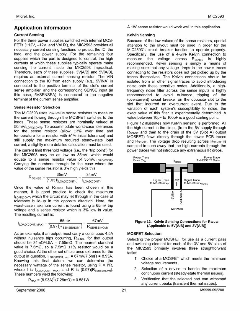
Kelvin Sensing Because of the low values of the sense resistors, special attention to the layout must be used in order for the MIC2593's circuit breaker function to operate properly. Specifically, the use of a 4-wire Kelvin connection to measure the voltage across RSENSE is highly recommended. Kelvin sensing is simply a means of making sure that any voltage drops in the power traces connecting to the resistors does not get picked up by the traces themselves. The Kelvin connections should be isolated from all other signal traces to avoid introducing noise onto these sensitive nodes. Additionally, a high-frequency noise filter across the sense inputs is highly recommended to avoid nuisance tripping of the (overcurrent) circuit breaker on the opposite slot to the slot that incurred an overcurrent event. Due to the variation of each system's susceptibility to noise, the exact value of this filter is experimentally determined. A value between 10pF to 100pF is a good starting point. Figure 12 illustrates how Kelvin sensing is performed. All the high current in the circuit (from the 5V supply through RSENSE and then to the drain of the 5V (Slot A) output MOSFET) flows directly through the power PCB traces and RSENSE. The voltage drop resulting across RSENSE is sampled in such away that the high currents through the power traces will not introduce any extraneous IR drops.
RSENSE
Power TraceFrom 5VIN
Power TraceTo MOSFET Drain
Signal Traceto MIC2593 VIN
Signal Traceto MIC2593 VSENSE
5VIN
A
5VS
EN
SE
A
MIC2593
22pF
Figure 12. Kelvin Sensing Connections for RSENSE (Applicable to 5V[A/B] and 3V[A/B])
MOSFET Selection Selecting the proper MOSFET for use as a current pass and switching element for each of the 3V and 5V slots of the MIC2593 primarily involves three straightforward tasks:
1. Choice of a MOSFET which meets the minimum voltage requirements.
2. Selection of a device to handle the maximum continuous current (steady-state thermal issues).
3. Verification that the selected part can withstand any current peaks (transient thermal issues).

Micrel, Inc. MIC2593
September 2008 22 M9999-092208
MOSFET Voltage Requirements The first voltage requirement for each MOSFET is easily stated: the drain-source breakdown voltage of the MOSFET must be greater than VIN(MAX) for the slot in question. For instance, the 5V input may reasonably be expected to see high-frequency transients as high as 6.5V. Therefore, the drain-source breakdown voltage of the MOSFET must be at least 7V. The second breakdown voltage criteria which must be met is a bit subtler than simple drain-source breakdown voltage, but is not hard to meet. Low-voltage MOSFETs generally have low breakdown voltage ratings from gate to source as well. In MIC2593 applications, the gates of the external MOSFETs are driven from the +12V input to the MIC2593 controller. That supply may well be at 12V + (5% x 12V) = 12.6V. At the same time, if the output of the MOSFET (its source) is suddenly shorted to ground, the gate-source voltage will go to (12.6V – 0V) = 12.6V. This means that the external MOSFETs must be chosen to have a gate-source breakdown voltage in excess of 13V; after 12V absolute maximum, the next commonly available voltage class has a 20V maximum gate-source voltage. At the present time, most power MOSFETs with a 20V gate-source voltage rating have a 30V drain-source breakdown rating or higher. As a general tip, look to surface mount devices with a drain-source rating of 30V as a starting point.
MOSFET Steady-State Thermal Issues The selection of a MOSFET to meet the maximum continuous current is a fairly straightforward exercise. First, arm yourself with the following data:
• The value of ILOAD(CONT, MAX) for the output in question (see Sense Resistor Selection).
• The manufacturer’s data sheet for the candidate MOSFET.
• The maximum ambient temperature in which the device will be required to operate.
• Any knowledge you can get about the heat sinking available to the device (e.g., Can heat be dissipated into the ground plane or power plane, if using a surface mount part? Is any airflow available?).
The data sheet will almost always give a value of on resistance given for the MOSFET at a gate-source voltage of 4.5V, and another value at a gate-source voltage of 10V. As a first approximation, add the two values together and divide by two to get the on-resistance of the part with 7V to 8V of enhancement (11.5V nominal VGATE minus the 3.5V to 4.5V gate threshold of the MOSFET). Call this value RON. Since a heavily enhanced MOSFET acts as an ohmic (resistive) device, almost all that’s required to determine steady-state power dissipation is to calculate I2R. The one addendum to this is that MOSFETs have a slight increase in RON with increasing die temperature. A good approximation for this
value is 0.5% increase in RON per °C rise in junction temperature above the point at which RON was initially specified by the manufacturer. For instance, if the selected MOSFET has a calculated RON of 10mΩ at TJ = 25°C and the actual junction temperature ends up at 110°C, a good first cut at the operating value for RON would be: [ ] 14.3mΩ25)(0.05)(110110mΩRON ≅−+≅
Next, approximate the steady-state power dissipation (I2R) using ILOAD(CONT,max) and the approximated RON.
[ ] 1.14W14.3mΩ(8.93A)RIR 2ON
2MAX)LOAD(CONT,ON ≅×≅×≅
The final step is to make sure that the heat sinking available to the MOSFET is capable of dissipating at least as much power (rated in °C/W) as that with which the MOSFET’s performance was specified by the manufacturer. Here are a few practical tips:
1. The heat from a surface-mount device such as an SO-8 MOSFET flows almost entirely out of the drain leads. If the drain leads can be soldered down to one square inch or more, the copper trace will act as the heat sink for the part. This copper trace must be on the same layer of the board as the MOSFET drain.
2. Airflow works. Even a few LFM (linear feet per minute) of air will cool a MOSFET down substantially. If you can, position the MOSFET(s) near the inlet of a power supply’s fan, or the outlet of a processor’s cooling fan.
3. The best test of a surface-mount MOSFET for an application (assuming the above tips show it to be a likely fit) is an empirical one. Check the MOSFET's temperature in the actual layout of the expected final circuit, at full operating current. The use of a thermocouple on the drain leads, or infrared pyrometer on the package, will then give a reasonable idea of the device’s junction temperature.
MOSFET Transient Thermal Issues Having chosen a MOSFET that will, a) withstand both the applied voltage stresses, and b) handle the worst-case continuous I2R power dissipation that it will endure; verifying the MOSFET’s ability to handle short-term overload power dissipation without overheating is the lone item to be determined. A MOSFET can handle a much higher pulsed power without damage than its continuous dissipation ratings would imply. The reason for this is that thermal devices (silicon die, lead frames, etc.) have thermal inertia. In terms related directly to the specification and use of power MOSFETs, this is known as “transient thermal impedance. ”Almost all power MOSFET data sheets give a Transient Thermal Impedance Curve. For example, take the case where tFLT for the 5V supply has been set to

Micrel, Inc. MIC2593
September 2008 23 M9999-092208
50ms, ILOAD(CONT, MAX) is 5.0A, the slow-trip threshold is 50Mv nominal, and the fast-trip threshold is 100mV. If the output is connected to a 0.60Ω load, the output current from the MOSFET for the slot in question will be regulated to 5.0A for 50ms before the MIC2593 circuit breaker trips. During that time, the dissipation in the MOSFET is given by:
[ ] 2V5A(0.6ΩA5VE IEP MOSFET =−=×=
( ) 50ms for 10W5A2VPMOSFET =×=
At first glance, it would appear that a really hefty MOSFET is required to withstand this sort of fault condition. This is where the transient thermal impedance curves become very useful. Figure 13 shows the curve for the Vishay (Siliconix) Si4430DY, a commonly used SO-8 power MOSFET. Taking the simplest case first, we’ll assume that once a fault event such as the one in question occurs, it will be a long time, several seconds, before the fault is isolated and the channel is reset. In such a case, we can approximate this as a “single pulse” event, that is to say, there’s no significant duty cycle. Then, reading up from the X-axis at the point where “Square Wave Pulse Duration” is equal to 0.1sec (=100msec), we see that the Zθ(JA) of this MOSFET to a highly infrequent event of this duration is only 7% of its continuous Rθ(JA). This particular part is specified as having an Rθ(JA) of 35°C/W for intervals of 10 seconds or less. Thus: Assume TA = 55°C maximum, 1 square inch of copper at the drain leads, no airflow. Recalling from our previous approximation hint, the part has an RON of (0.014/2) = 7mΩ at 25°C. Assume it has been carrying just about 5A for some time. When performing this calculation, be sure to use the highest anticipated ambient temperature (TA(MAX)) in which the MOSFET will be operating as the starting
temperature, and find the operating junction temperature increase (∆TJ) from that point. Then, as shown next, the final junction temperature is found by adding TA(MAX) and ∆TJ. Since this is not a closed-form equation, getting a close approximation may take one or two iterations, but it’s not a hard calculation to perform and tends to converge quickly. Then the starting (steady-state) TJ is:
JA(MAX)J ΔTTT +≅
[ ])C)(R)(0.005T(TRT ONAA(MAX)ONA(MAX) °−++≅
θ(JA)2 RI ××
[ ]7mΩmC)(0.005)(25C(557mΩC55TJ °−°++°≅
C/W)(35(5A)2 °××
C)(35(0.20125W)C55TJ °+°≅
C62.0°≅ Iterate the calculation once to see if this value is within a few percent of the expected final value. For this iteration we will start with TJ equal to the already calculated value of 62.0°C:
[ ]7mΩmC)(0.005)(25C(62.07mΩTT AJ °−°++≅
C/W)(35(5A)2 °××
C62.35C)(35(0.20125W)C55TJ °≅°+°≅
So our original approximation of 62.0°C was very close to the correct value. We will use TJ = 62°C. Finally, add (10W)(35°C/W)(0.07) = 24.5°C to the steady-state TJ to get TJ(TRANSIENT MAX.) = 86.5°C. This is an acceptable maximum junction temperature for this part.
10-4 10-3 10-2 10-1 1 10 100 600
2
1
0.1
0.01
0.2
0.1
0.05
0.02
Single Pulse
Duty Cycle = 0.5
Normalized Thermal Transient Imperance, Juction-to-Ambient
1. Duty Cycle, D =2. Per Unit Base = RqJA = 67°C/W3. TJM – TA = PDMZqJA
(t)
4. Surface Mounted
t1t2
t1t2
Notes:
PDM
Square Wave Pulse Duration (sec)
Nor
mal
ized
Effe
ctiv
eTr
ansi
ent
Ther
mal
Impe
danc
e
Figure 13. Si4430DY MOSFET Transient Thermal Impedance Curve

Micrel, Inc. MIC2593
September 2008 24 M9999-092208
MOSFET and Sense Resistor Selection Guide Listed in Table 5 below, by Manufacturer and Type Number, are some of the more popular MOSFET and resistor types used in PCI hot plug applications. Although far from comprehensive, this information will constitute a good starting point for most designs.
Power Supply Decoupling In general, prudent system design requires that power supplies used for logic functions should have less than 100mV of noise at frequencies of 100kHz and above. In particular, the –12V supply should have less than 100mV of peak-to-peak noise at frequencies of 1MHz or higher. This is because the –12V supply is the most negative potential applied to the IC, and is therefore connected to the device's substrate. All of the subcircuits integrated onto the silicon chip are hence subjected by capacitive coupling to any HF noise on the –12V supply. While individual capacitances are quite low, the amount of injected energy required to cause a "glitch" can also be quite low at the internal nodes of high speed logic circuits. Less obviously, but equally important, is the fact that the internal charge pump for the 3.3VAUX supplies is somewhat susceptible to noise on the +12V input when that input is at or near zero volts. The +12V supply should not carry HF noise in excess of 200mV peak-to-peak with respect to chip ground when it is in the "off" state. If either the –12V input, the +12V input, of both supplies do carry significant HF noise (as can happen when they are locally derived by a switching converter), the solution
is both small and inexpensive. An LC filter made of a ferrite bead between the noisy power supply input and the MIC2593, followed by a "composite capacitor" from the affected MIC2593 input pin to ground, will suffice for almost any situation. A good composite capacitor for this purpose is the parallel combination of a 47µF tantalum bulk decoupling capacitor, and one 1µF and one 0.01µF ceramic capacitor for high-frequency bypass. A suggested ferrite bead for such use is Fair-Rite Products Corporation part number 2743019447 (this is a surface-mountable part). Similar parts from other vendors or a 0.27µH air-core coil can also be used. Noisy VIN To MIC2593
SMT Ferrite BeadFair-Rite ProductsType 2743019447
47µFTanalum
1µFCeramic
10nFCeramic
Figure 14. Filter Circuit for Noisy Supplies (+3.3V and/or –12V)
It is theoretically possible that high-amplitude, HF noise reflected back into one or both of the MIC2593’s –12V outputs could interfere with proper device operation, although such noisy loads are unlikely to occur in the real world. If this becomes an application-specific concern, a pair of filters similar to that in Figure 14 will provide the required HF bypassing. The capacitors would be connected to the MIC2593’s –12V output pins, and the ferrite beads would be placed between the –12V output pins and the loads.
MOSFET Vendors Key MOSFET Type(s) Web Address Vishay (Siliconix) Si4430DY (“LittleFoot®” Series)
Si4420DY (“LittleFoot®” Series) www.siliconix.com
International Rectifier IRF7413A (SO-8 package part) Si4420DY (second source to Vishay)
www.irf.com
Fairchild Semiconductor FDS6644 (SO-8 package part) FDS6670A (SO-8 package part) FDS6688 (SO-8 package part)
www.fairchildsemi.com
Resistor Vendors Sense Resistors Web Address
Vishay (Dale) WSL Series WSL 3637 Series
www.vishay.com/docs/wsl_30100.pdf
IRC OARS Series LR Series
(second source to WSL)
irctt.com/pdf_files/OARS.pdf irctt.com/pdf_files/LRC.pdf
Micrel, Inc. MIC2593
September 2008 25 M9999-092208
–12V Input Clamp Diode The –12V input to the MIC2593 is the most negative potential on the part and is therefore connected to the chip’s substrate (as described in “Power Supply Decoupling,” above). Although no particular sequencing of the –12V supply relative to the other MIC2593 supplies is required for normal operation, this substrate connection does mean that the –12V input must never exceed the voltage on the GROUND pin of the IC by more than 0.3 volts. Small amounts of internal leakage current can cause this to happen when the VSTBY pins are energized and the 12MVIN pins are not energized. In addition, power supply output ringing or L(di/dt) effects in the wiring and on the PCB itself will cause brief transient voltages in excess of +0.3V to appear at the –12V input. For this reason, it is required to clamp the –12V input to ground with a Schottky diode. A diode rated at 1 amp and 20V to 40V as shown in our application schematic diagram is suggested. The diode’s anode should be physically placed directly at the –12V input to the MIC2593, and its cathode should have as short a path as possible back to the part’s ground. A good SMT part for this application is a type MBRS140T3 (1A, 40V).
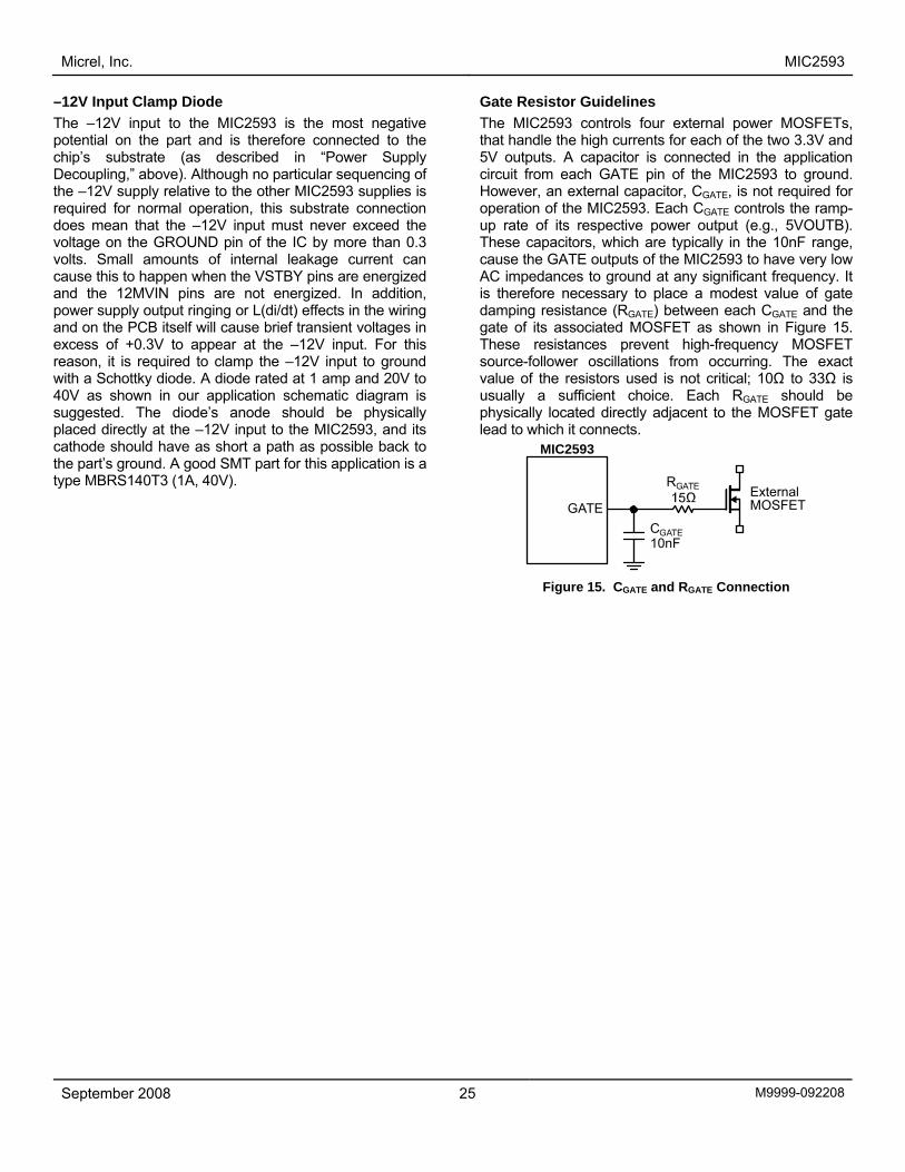
Gate Resistor Guidelines The MIC2593 controls four external power MOSFETs, that handle the high currents for each of the two 3.3V and 5V outputs. A capacitor is connected in the application circuit from each GATE pin of the MIC2593 to ground. However, an external capacitor, CGATE, is not required for operation of the MIC2593. Each CGATE controls the ramp-up rate of its respective power output (e.g., 5VOUTB). These capacitors, which are typically in the 10nF range, cause the GATE outputs of the MIC2593 to have very low AC impedances to ground at any significant frequency. It is therefore necessary to place a modest value of gate damping resistance (RGATE) between each CGATE and the gate of its associated MOSFET as shown in Figure 15. These resistances prevent high-frequency MOSFET source-follower oscillations from occurring. The exact value of the resistors used is not critical; 10Ω to 33Ω is usually a sufficient choice. Each RGATE should be physically located directly adjacent to the MOSFET gate lead to which it connects.
MIC2593
GATE
RGATE
CGATE10nF
ExternalMOSFET
Figure 15. CGATE and RGATE Connection

Micrel, Inc. MIC2593
September 2008 26 M9999-092208
Package Information
,SNOISURTORPROHSALFDLOMEDULCNITONSEODNOISNEMID.MM452.0DEECXETONLLAHSHCIHWFOREHTIE
.NOISURTORPRABMADEDULCNITONSEODNOISNEMIDDAELMOTTOBNAHTRELLAMSERASNOISNEMIDDLOMPOTEGAKCAP
GNAHREVOTONLLIWEGAKCAPFOPOTDNASNOISNEMIDDLOM.EGAKCAPFOMOTTOB
:SETON
.1
.2
.3
.4
48-Pin TQFP (TQ)
MICREL, INC. 2180 FORTUNE DRIVE SAN JOSE, CA 95131 USA TEL +1 (408) 944-0800 FAX +1 (408) 474-1000 WEB http://www.micrel.com
The information furnished by Micrel in this data sheet is believed to be accurate and reliable. However, no responsibility is assumed by Micrel for its
use. Micrel reserves the right to change circuitry and specifications at any time without notification to the customer.
Micrel Products are not designed or authorized for use as components in life support appliances, devices or systems where malfunction of a product can reasonably be expected to result in personal injury. Life support devices or systems are devices or systems that (a) are intended for surgical implant
into the body or (b) support or sustain life, and whose failure to perform can be reasonably expected to result in a significant injury to the user. A Purchaser’s use or sale of Micrel Products for use in life support appliances, devices or systems is a Purchaser’s own risk and Purchaser agrees to fully
indemnify Micrel for any damages resulting from such use or sale.
© 2002 Micrel, Incorporated.