Embed Size (px)
Citation preview
Applied Surface Science 70/71 (1993) 53-57
North-Holland
MeV ion channeling deposition methods
applied surface science
study of SiN,/Si interfaces formed by various
Jong Moon, Toshimichi Ito and Akio Hiraki Department of Electrical Engineering, Osaka University, Suita, Osaka 565, Japan
Received 24 August 1992; accepted for publication 18 November 1992
A MeV ion channeling study on the interface abruptness and film stoichiometry of SiNJSi systems has been accomplished.
The SIN, films were formed by means of direct nitridation (DN) on a Si substrate, low-pressure chemical vapor deposition
(LPCVD), and plasma-assisted chemical vapor deposition (PACVD). The compositions of the films were observed to have the
values of Si,N,., for DN, Si,N, for LPCVD, and SisN,,, for PACVD. The SiNJSi system formed by DN shows the most abrupt
interface (4 ML) among the three (- 9 ML for LPCVD and - 10 ML for PACVD). In electrical measurements, a lower leakage
current (- 10-t’ A) and a higher breakdown voltage (11.9 MV/cm) were observed for the DN sample than those for either of the
CVD ones. These results demonstrate that there is a strong correlation between leakage current and interface abruptness of the
SiN,/Si system.
1. Introduction
Silicon nitride film is a good dielectric with a higher dielectric constant than SiO,, and is being used in ultra-large-scale integration (ULSI) and especially in dynamic random access memory (DRAM) cells as a capacitor dielectric. Physical, electrical, and structural properties of Si,N, films on Si substrates change with the exact conditions of the deposition and growth methods. Com- monly used methods are direct nitridation (DN) by nitrogen plasma [l], thermal nitridation of SiO, film [2], and vapor-phase growth methods such as low-pressure chemical vapor deposition (LPCVD) [3] and low-temperature (N 400°C) plasma-assisted chemical vapor deposition (PACVD) [4]. Because very thin SiN, films (be- low 10 nm> are strongly demanded for the capaci- tor dielectric, the SiNJSi interface has a signifi- cant meaning. Thus, many works on the electrical properties have been done using deep-level tran- sient spectroscopy (DLTS) and capacitance-volt- age methods [5-71. On the other hand, for the physical properties, transmission electron mi- croscopy (TEMI [l] and MeV ion channeling by
Rutherford backscattering spectrometry (RBS) [8] have revealed the SiNJSi interfaces to be fairly abrupt. Using TEM, Paloura et al. [5] have shown that the interface formed by the DN method is uniform and abrupt with a transition region con- fined to about 6 A. Smith et al. [S] have used the ion channeling technique to show that there is a disordered region of N 7 ML below the SiN, film deposited by LPCVD.
In this paper, we report on the stoichiometry and interface properties of silicon nitride films formed by LPCVD, PACVD, and DN methods using the ion channeling technique. Furthermore, electrical properties such as leakage current and breakdown voltage are discussed in relation to the hydrogen content in the films.
2. Experimental
A directly nitrided SiN, film was grown on a Si substrate in a N, plasma generated by the elec- tron cyclotron resonance (ECR) method. The process parameters used for the SiN, formation are summarized briefly in table 1. Details of these
0169-4332/93/$06.00 0 1993 - Elsevier Science Publishers B.V. All rights reserved

54 J. Moon et al. / MeV ion channeling study of SiN, /Si interfaces
formation processes can be found in refs. [3,4,9]. The thickness of the films examined in this exper- iment was fixed at 1000 f 50 A. Ion channeling measurements were performed in a sequential fashion as a function of SiN, thickness following step-by-step removal of the film in a dilute HF solution. These were accomplished with 1.0 MeV 4He+ in a scattering chamber with a pressure of - lo-’ Torr which was coupled to a 1.1 MeV Pelletron accelerator. The details of the ion chan- neling technique are described in the literature [lo]. Silicon nitride films were analyzed by detect- ing ions scattered glancingly from near 85” rela- tive to the incident beam direction. Area1 densi- ties were determined with nitrogen-implanted sil- icon as a standard sample using the known stop- ping powers of 4Het in Si. The beam dose for each spot on the sample was kept constant at 2 PC in order to avoid possible beam-induced dam- age. Hydrogen contents in the SiN, films were determined using the elastic recoil detection (ERD) technique with a primary beam of 2.4 MeV He ions. Recoiling protons were detected at a scattering angle of 30”. Forward-scattered He ions and all recoiling particles except for the protons were stopped in a 10 pm thick aluminum foil.
3. Results and discussion
3.1. Ion channeling
Fig. 1 shows a channeling spectrum along the [lo01 axis of SKlOO) with an SiN, overlayer formed by the DN method. The Si and N peaks are well
3 : - lMeVHe+ s 33 _ b Si T) I -
s N ; I -
Channel number
Fig. 1. Typical channeling spectrum of SIN, /Si(lOO) along the
[loo] axis using 1 MeV 4Hef. Filled areas show background
areas used for subtraction.
separated due to the large difference in their kinematic factors. The background signal under the N peak is due to the backscattering of dechanneled He ions from the Si substrate and was easily subtracted using the trapezoidal rule. On the other hand, the background subtraction for the Si peak was accomplished by two meth- ods: the conventional triangular method as shown in fig. 1 was used for thin SiN, films of thick- nesses below - 100 A. A modified triangular method was employed for thick films with thick- nesses above - 100 A. The details of these meth- ods have been described in the literature [ll].
A plot of the Si concentration versus N con- centration can give (1) the average compositions evaluated from the slopes of the straight lines and (2) the SiNJSi interfacial thicknesses esti- mated from the Si concentrations extrapolated at zero N coverage. These extrapolated values con- tain the following two contributions: (1) displaced Si atoms in the amorphous SiN, layer, and (2) the intrinsic Si surface peak (SP). The latter is pro- duced by the first few atoms in each row of the substrate Si crystal which are visible to the inci-
Table 1
Process conditions and the resultant physical properties of the interface and bulk for silicon nitride films
Film Process gas Process Frequency Power Pressure Refractive Atomic Inteface
formation temperature (MHz) W) (Torr) index ratio layer
methods (“0 (N/W (ML)
LPCVD SiH,Cl, : NH, 820 0.2 2.01 f 0.02 1.34 -9
(= 1:4)
PACVD SiH,:NH, 420 13.56 1000 1.0 2.06 + 0.05 1.27 - 10
(1: 10)
DN N2 4.50 2.45 x lo3 500 0.1 1.95 f 0.05 1.42 4
1 ML = 6.8 X lOI4 atoms/cm* for Si(lO0).
J. Moon et al. / MeV ion channeling study of SiNx / Si interfaces 55
dent ion beam as schematically shown in the inset of fig. 2. The Si SP intensity for the ideal [loo] string can be easily calculated from a Monte Carlo computer program. The resulting value of the SP intensity was 2.93 atoms/row (= 7.97 x
1Or5 cmp2) for 1 MeV He ions. This value can be used for the evaluation of the SP contribution to the interface peak intensity.
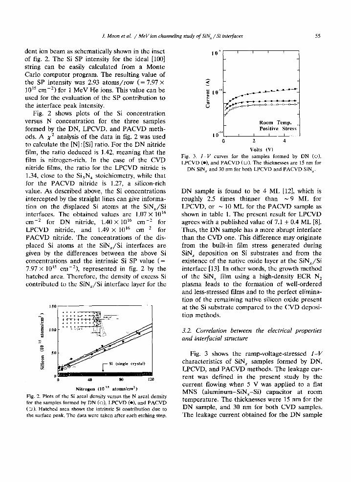
Fig. 2 shows plots of the Si concentration versus N concentration for the three samples formed by the DN, LPCVD, and PACVD meth- ods. A x2 analysis of the data in fig. 2 was used to calculate the [Nl : [Si] ratio. For the DN nitride film, the ratio deduced is 1.42, meaning that the film is nitrogen-rich. In the case of the CVD nitride films, the ratio for the LPCVD nitride is 1.34, close to the Si,N, stoichiometry, while that for the PACVD nitride is 1.27, a silicon-rich value. As described above, the Si concentrations intercepted by the straight lines can give informa- tion on the displaced Si atoms at the SiN,/Si interfaces. The obtained values are 1.07 x 10¹⁶ cmp2 for DN nitride, 1.40 X 1Or6 cme2 for LPCVD nitride, and 1.49 x 1016 cm-* for PACVD nitride. The concentrations of the dis- placed Si atoms at the SiNJSi interfaces are given by the differences between the above Si concentrations and the intrinsic Si SP value (= 7.97 X 1015 cm-*), represented in fig. 2 by the hatched area. Therefore, the density of excess Si contributed to the SiNJSi interface layer for the
z - 50 E B
‘L ;ij
Si (single crystal)
0 0 40 80 120
Nitrogen (10 IS atoms/cmz)
Fig. 2. Plots of the Si area1 density versus the N area1 density for the samples formed by DN CO), LPCVD (a), and PACVD (0). Hatched area shows the intrinsic Si contribution due to the surface peak. The data were taken after each etching step.
0 2 4
Volts (V) Fig. 3. I-V curves for the samples formed by DN (o),
LPCVD (01, and PACVD (0 ). The thicknesses are 15 nm for DN SIN, and 30 nm for both LPCVD and PACVD SiN,.
DN sample is found to be 4 ML [12], which is roughly 2.5 times thinner than N 9 ML for LPCVD, or N 10 ML for the PACVD sample as shown in table 1. The present result for LPCVD agrees with a published value of 7.1 + 0.4 ML [8]. Thus, the DN sample has a more abrupt interface than the CVD one. This difference may originate from the built-in film stress generated during SIN, deposition on Si substrates and from the existence of the native oxide layer at the SiNJSi interface [13]. In other words, the growth method of the SiN, film using a high-density ECR N, plasma leads to the formation of well-ordered and less-stressed films and to the perfect elimina- tion of the remaining native silicon oxide present at the Si substrate compared to the CVD deposi- tion methods.
3.2. Correlation between the electrical properties and interfacial structure
Fig. 3 shows the ramp-voltage-stressed Z-V characteristics of SiN, samples formed by DN, LPCVD, and PACVD methods. The leakage cur- rent was defined in the present study by the current flowing when 5 V was applied to a flat MNS (aluminum-SiN,-Si) capacitor at room temperature. The thicknesses were 15 nm for the DN sample, and 30 nm for both CVD samples; The leakage current obtained for the DN sample

56 .I. Moon et al. / MeV ion channeling study of SiN, /Si interfaces
is 7.8 X lo-” A, rather low in comparison with 2.3 x lo-” A for the LPCVD sample, and 7.8 X
lo-” A for the PACVD sample. A correction for the thickness difference in the DN and CVD samples meant even a better leakage-current property of the DN sample. The breakdown volt- age measured for the DN sample is 11.9 MV/cm, higher than those for the LPCVD sample (9.6 MV/cm) and the PACVD sample (5.3 MV/cm). These results are consistent with the results on the interfacial abruptness.
The lower leakage current and higher break- down voltage characteristic of the SiN, film formed by DN can be attributed to the assump- tions (1) that highly activated electrons generated by the ECR N, plasma break and eliminate the strained surface Si-0 bonds while for CVD methods, the activated species generated by the energies of the RF plasma or a temperature below 950°C are insufficient to break Si-0 bonds in the initial stage of nitridation [4,14,15], and (2) that since the highly activated nitriding species tend to react preferentially with the defects, bulk and interfaces of SiN, films formed in the high- density ECR N, plasma have less defect density.
In the case of both CVD samples, although the interface abruptness is almost the same, there is a significant difference in the breakdown voltage and leakage current. This difference can be at- tributed to the different bulk properties between both SIN, films, which may come from the lower formation temperature (N 420°C) for PACVD than that for LPCVD (- 820°C). The observed
0 80 160 Channel Number
Fig. 4. He ERD spectra for (a) the SiN, film formed by PACVD and (b) the SiN, film formed by LPCVD, showing the distribution of hydrogen in the samples. The thicknesses were fixed at 100 nm. The “S” arrow indicates the surface
position of hydrogen.
difference in the electrical properties can be ex- plained by (1) that the PACVD sample has a large amount of defects in the film such as Si dangling bonds, nitrogen vacancies, and Si vacan- cies, and (2) that the hydrogen contents, which exist in the form of unbonded hydrogen, N-H bonds, and Si-H bonds, are 4.3 times larger in the PACVD sample (- 13%) than those for the LPCVD one (3%), as shown in fig. 4. A larger content of hydrogen causes the SiN, film to be less dense and more porous. Thus, the LPCVD sample has better electrical properties than the PACVD one.
4. Conclusions
We have analyzed the SiN,/Si interfaces using MeV ion channeling and correlated the structural data with the electrical properties of SIN, films formed by means of three different techniques. The ion channeling results show that the inter- face of the DN sample is the most abrupt, being 4 ML. The DN films show a lower leakage current and higher breakdown voltage than the CVD SIN, films. The control of SiNJSi interfaces as well as the bulk structure including the amounts of hydrogen incorporated, can lead to a higher quality of thin SIN, films.
References
[l] E.C. Paloura, K. Nauka, J. Lagowski and H.C. Gatos, Appl. Phys. Lett. 49 (1986) 97.
[2] M. Delfino, J.A. Fair and S. Salimian, Appl. Phys. Lett. 60 (1992) 341.
[3] A.E.T. Kuiper, S.W. Koo, F.H.P.M. Habraken and Y. Tamminga, J. Vat. Sci. Technol. B 1 (1983) 62.
[4] Y. Manabe and T. Mitsuyu, .I. Appl. Phys. 66 (1989) 2475. [5] E.C. Paloura, J. Lagowski and H.C. Gatos, J. Appl. Phys.
69 (1991) 3995. [61 W. Ting, J. Ahn and D.L. Kwong, J. Appl. Phys. 70
(1991) 3934. [7] M.M. Moslehi and K.C. Saraswat, IEEE Trans. Electron
Devices ED-32 (1985) 106. [81 G.A. Smith, Li Luo and W.M. Gibson, J. Vat. Sci.
Technol. A 8 (1990) 1427. [9] J. Moon, T. Ito and A. Hiraki, Thin Solid Films, to be
published.

J. Moon et al. / MeV ion channeling study of SirU, / Si interfaces 57
[lo] L.C. Feldman, J.W. Mayer and S.T. Picraux, Material Analysis by Ion channeling (Academic Press, New York, 1982).
[ll] T. Ito, Jpn. J. Appl. Phys. 25 (1986) 902. [12] 1 atom/row = 2.7~ 1015 cm-’ and 1 ML = 6.8~ 1014
cm-* for the Si(100).
[13] F.H.P.M. Habraken, A.E.T. Kuiper, A. van Oostrom and Y. Tamminga, J. Appl. Phys. 53 (1982) 404.
[14] R.P. Vasquez and A. Madhukar, Appl. Phys. Lett. 47 (1985) 998.
[15] H. Amemiya, H. Oyama and Y. Sakamoto, J. Phys. Sot. Jpn. 56 (1987) 2401.


![Channeling Experiments with Electrons at the Mainz ... · Photon energy: < 5 MeV (Channeling Radiation) 0 50 100 150 200 250 300 0,00 0,05 0,10 0,15 0,20 0,25 0,30 U.] No saturation](https://img.dokumen.tips/doc/110x75/5f1c83c861dae6187b2cf36e/channeling-experiments-with-electrons-at-the-mainz-photon-energy-5-mev.jpg)