Embed Size (px)
Citation preview
2011.10.5
Hiroyuki Fujita, Agnes-Tixier Mita, Hiroshi Toshiyoshi
Center for International Research on Micronano
Mechatronics
IIS, The University of Tokyo
MEMS-CMOS Integration
and Beyond
2011.10.5
Content
• MEMS trend toward MEMS-CMOS
integration
• Examples of MEMS-CMOS integration
• Beyond MEMS-CMOS integration
2011.10.5
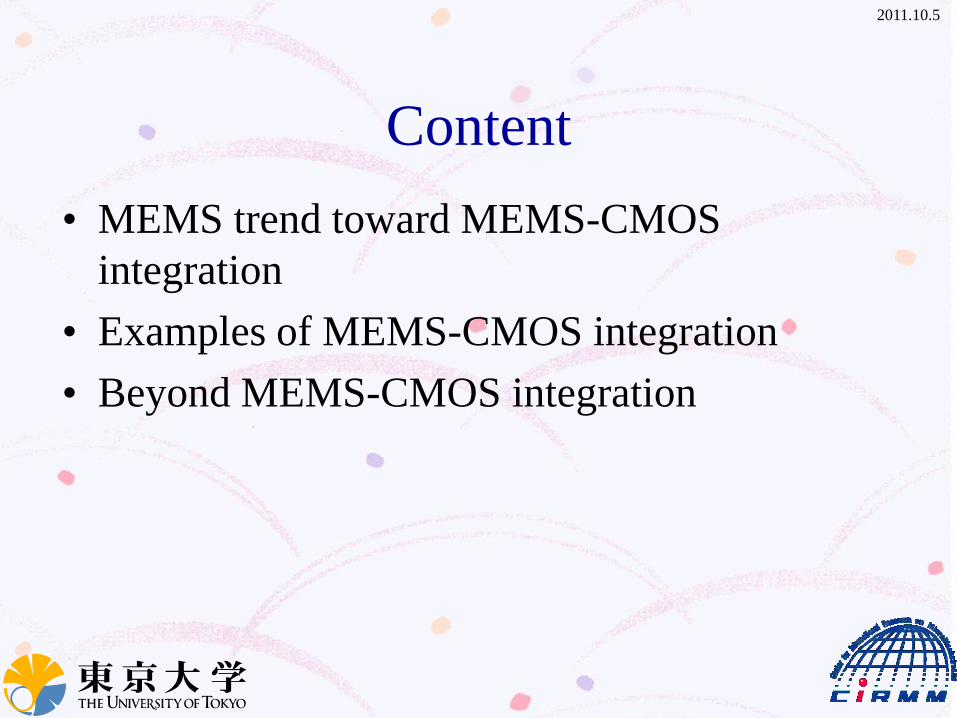
Examples of MEMS devices U-Tokyo
AD Denso
UC Berkeley Northeastern Univ.
Olympus
IEMN/CNRS
2011.10.5
MEMS Development in Last Decade
• Almost all the important processes and devices in
micro-scale already existed 10 years ago, e.g. DRIE,
bonding, microactuators, etc.
• Technological sophistication,
• Application diversity increase
• Performance improvement.
• Commercial products have flourished.
2011.10.5
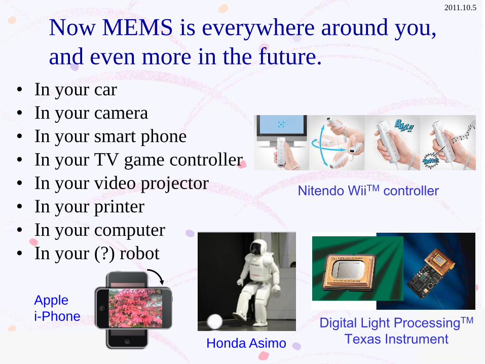
Now MEMS is everywhere around you,
and even more in the future.
• In your car
• In your camera
• In your smart phone
• In your TV game controller
• In your video projector
• In your printer
• In your computer
• In your (?) robot
Digital Light ProcessingTM
Texas Instrument
Nitendo WiiTM controller
Honda Asimo
Apple
i-Phone
2011.10.5
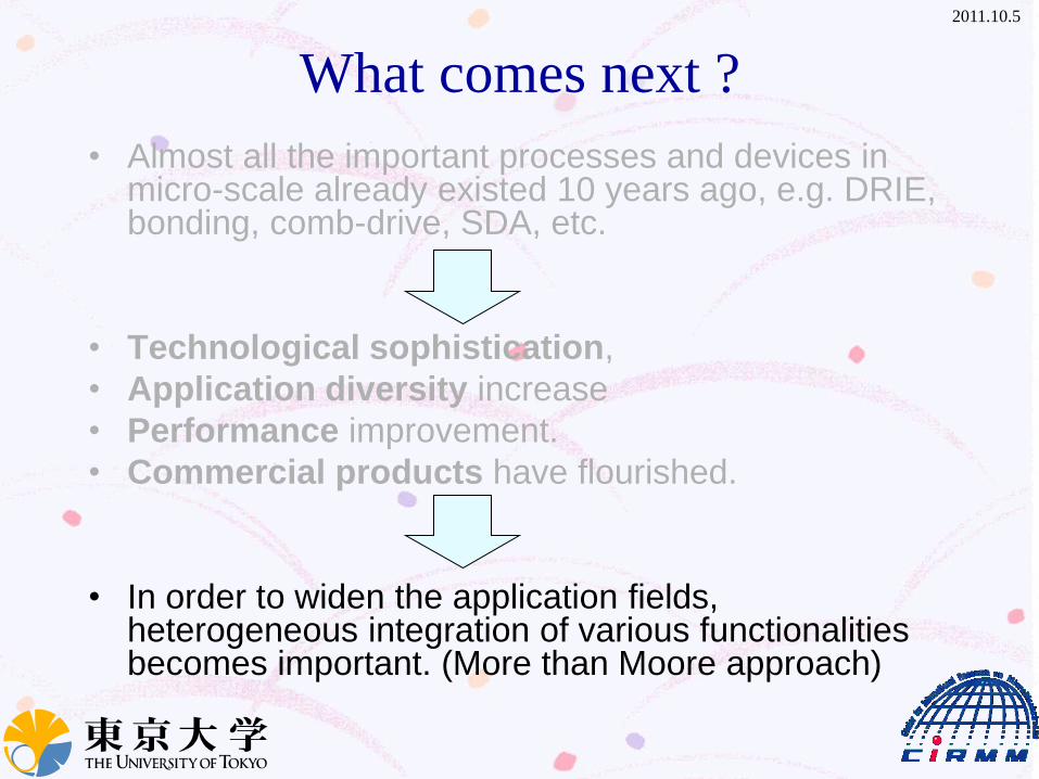
What comes next ?
• Almost all the important processes and devices in micro-scale already existed 10 years ago, e.g. DRIE, bonding, comb-drive, SDA, etc.
• Technological sophistication,
• Application diversity increase
• Performance improvement.
• Commercial products have flourished.
• In order to widen the application fields, heterogeneous integration of various functionalities becomes important. (More than Moore approach)
2011.10.5
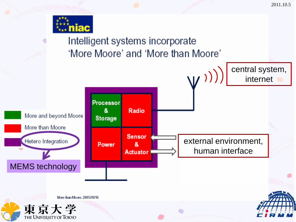
MEMS technology
central system,
internet
external environment,
human interface
2011.10.5
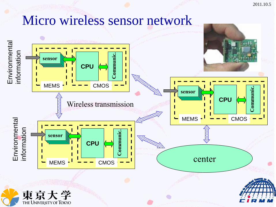
center
Micro wireless sensor network
Wireless transmission
センサ CPU .
センサ センサ sensor
MEMS CMOS
Environm
enta
l
info
rmation
Co
mm
un
ic.
センサ CPU .
センサ センサ sensor
MEMS CMOS
Environm
enta
l
info
rmation
Co
mm
un
ic.
センサ CPU .
センサ センサ sensor
MEMS CMOS
Co
mm
un
ic.
2011.10.5
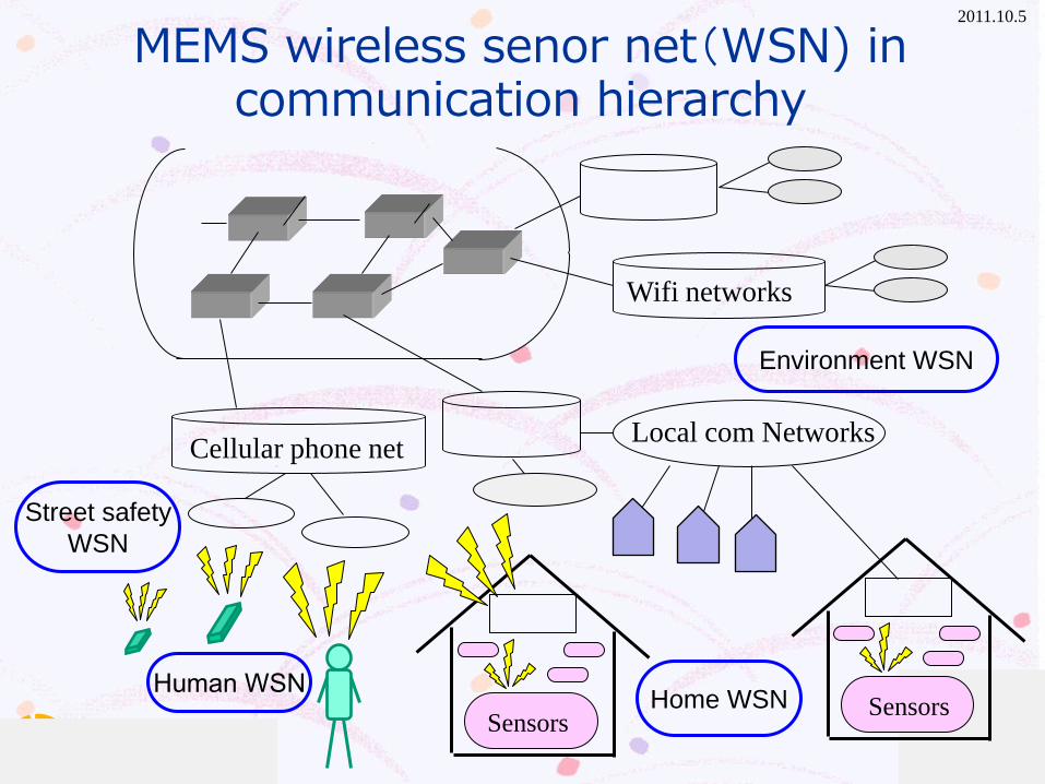
Home WSN
MEMS wireless senor net(WSN) in communication hierarchy
Local com Networks Cellular phone net
Wifi networks
Sensors Sensors
Human WSN
Environment WSN
Street safety
WSN

2011.10.5
Content
• MEMS trend toward MEMS-CMOS
integration
• Examples of MEMS-CMOS integration
• Beyond MEMS-CMOS integration
2011.10.5
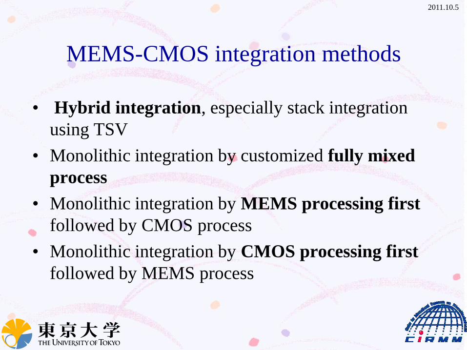
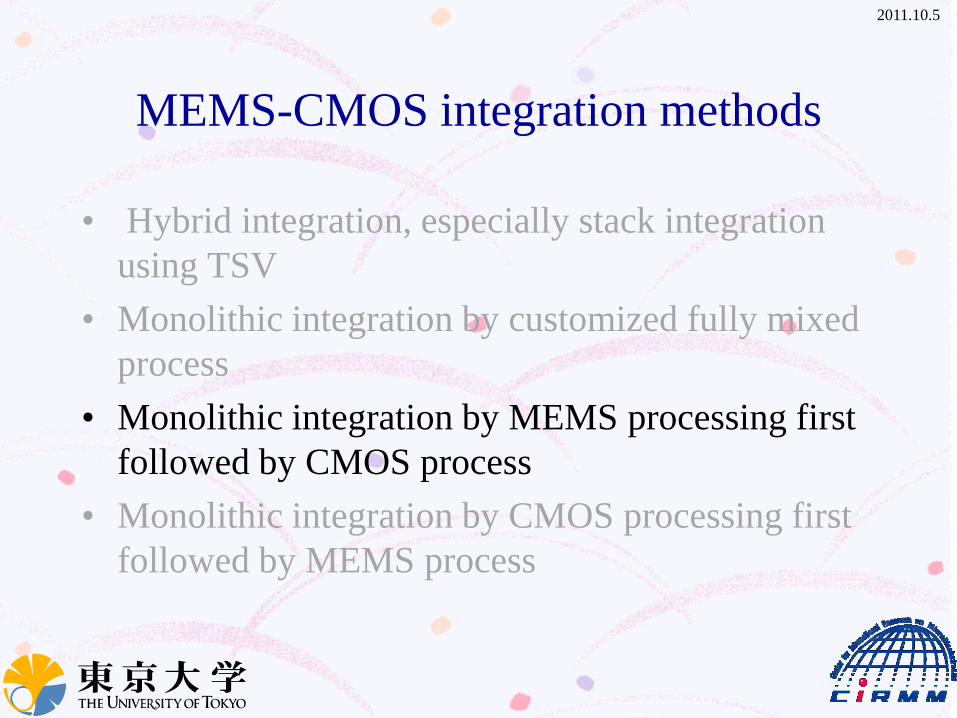
MEMS-CMOS integration methods
• Hybrid integration, especially stack integration
using TSV
• Monolithic integration by customized fully mixed
process
• Monolithic integration by MEMS processing first
followed by CMOS process
• Monolithic integration by CMOS processing first
followed by MEMS process
2011.10.5
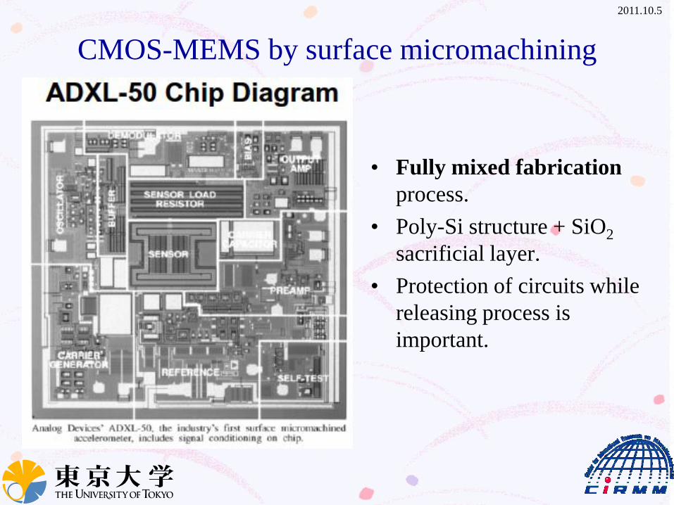
CMOS-MEMS by surface micromachining
• Fully mixed fabrication
process.
• Poly-Si structure + SiO2
sacrificial layer.
• Protection of circuits while
releasing process is
important.
2011.10.5
MEMS-CMOS integration methods
• Hybrid integration, especially stack integration
using TSV
• Monolithic integration by customized fully mixed
process
• Monolithic integration by MEMS processing first
followed by CMOS process
• Monolithic integration by CMOS processing first
followed by MEMS process

2011.10.5
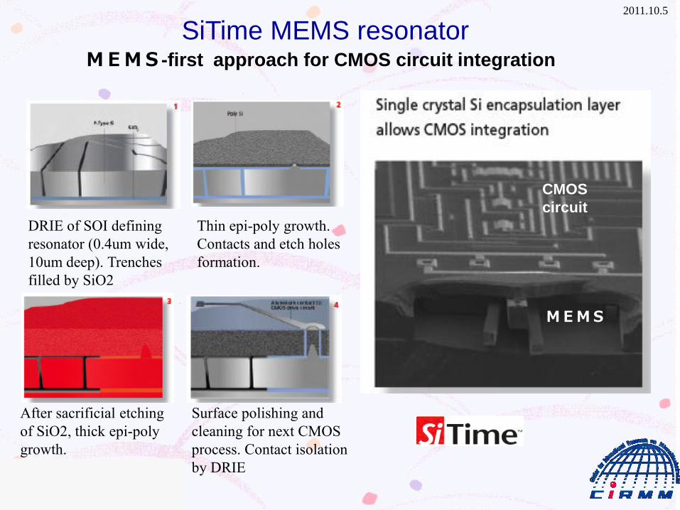
SiTime MEMS resonator
http://www.sitime.jp/
MEMS-first approach for
CMOS circuit integration
2011.10.5
SiTime MEMS resonator MEMS-first approach for CMOS circuit integration
CMOS
circuit
MEMS
DRIE of SOI defining
resonator (0.4um wide,
10um deep). Trenches
filled by SiO2
Thin epi-poly growth.
Contacts and etch holes
formation.
After sacrificial etching
of SiO2, thick epi-poly
growth.
Surface polishing and
cleaning for next CMOS
process. Contact isolation
by DRIE
2011.10.5
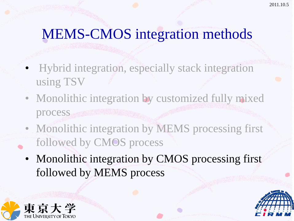
MEMS-CMOS integration methods
• Hybrid integration, especially stack integration
using TSV
• Monolithic integration by customized fully mixed
process
• Monolithic integration by MEMS processing first
followed by CMOS process
• Monolithic integration by CMOS processing first
followed by MEMS process
2011.10.5
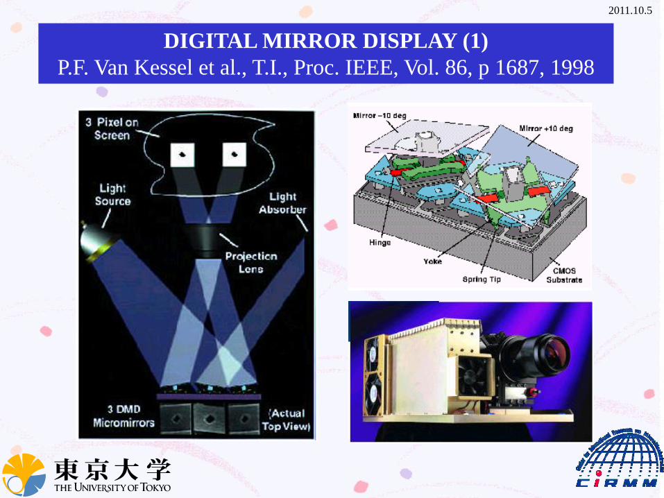
DIGITAL MIRROR DISPLAY (1)
P.F. Van Kessel et al., T.I., Proc. IEEE, Vol. 86, p 1687, 1998
2011.10.5
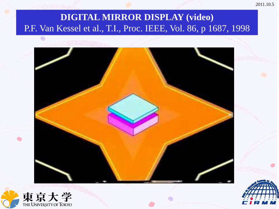
DIGITAL MIRROR DISPLAY (video)
P.F. Van Kessel et al., T.I., Proc. IEEE, Vol. 86, p 1687, 1998
2011.10.5
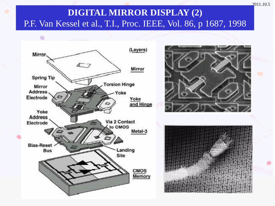
DIGITAL MIRROR DISPLAY (2)
P.F. Van Kessel et al., T.I., Proc. IEEE, Vol. 86, p 1687, 1998
2011.10.5
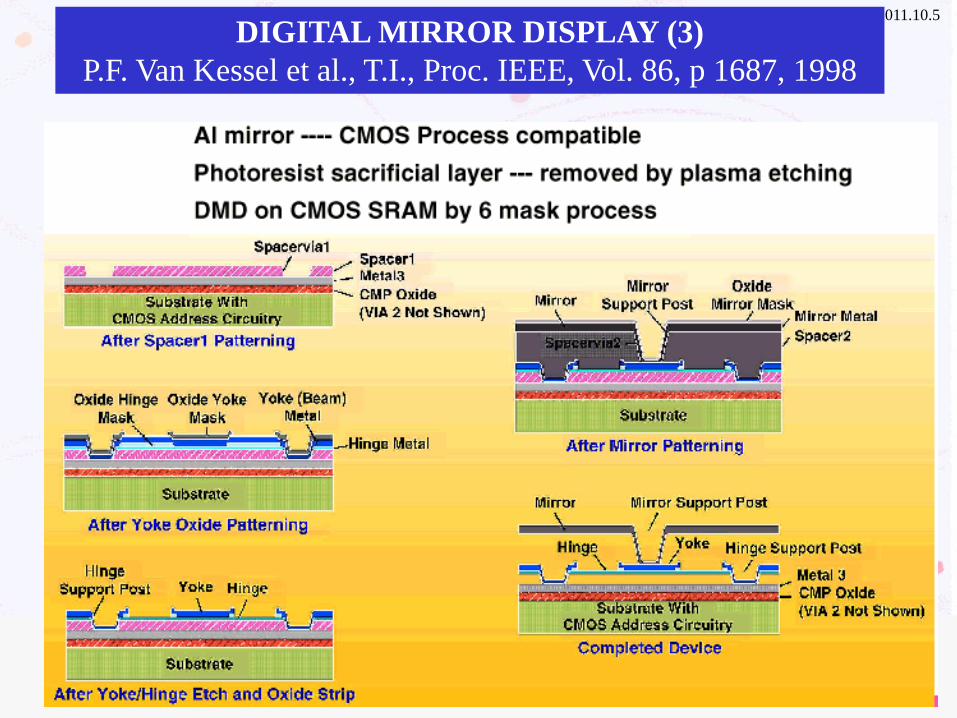
DIGITAL MIRROR DISPLAY (3)
P.F. Van Kessel et al., T.I., Proc. IEEE, Vol. 86, p 1687, 1998
2011.10.5
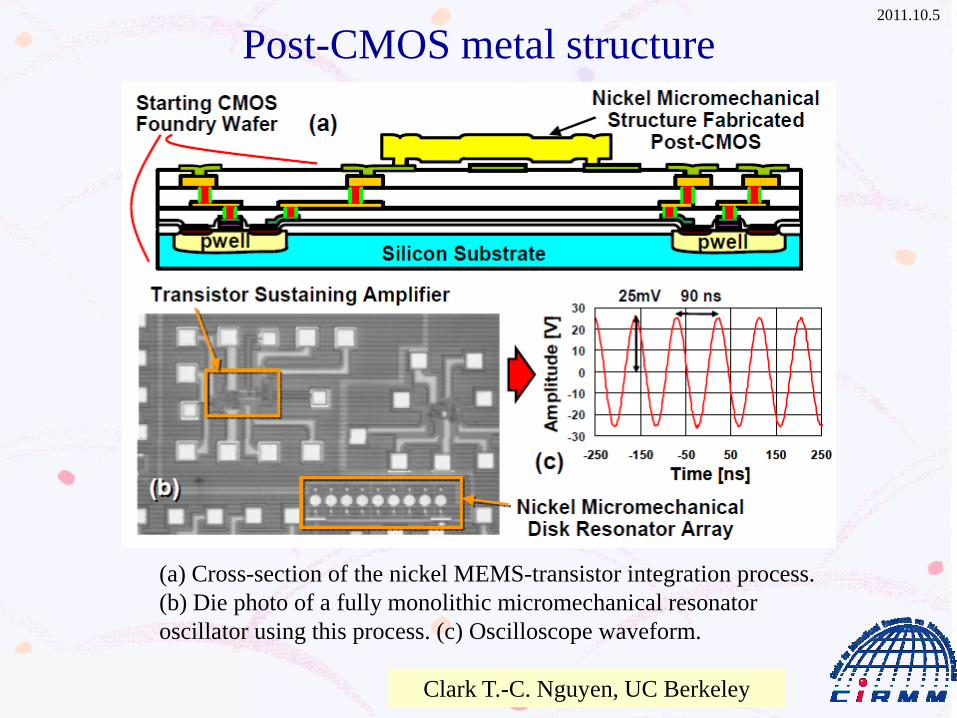
(a) Cross-section of the nickel MEMS-transistor integration process.
(b) Die photo of a fully monolithic micromechanical resonator
oscillator using this process. (c) Oscilloscope waveform.
Post-CMOS metal structure
Clark T.-C. Nguyen, UC Berkeley
2011.10.5
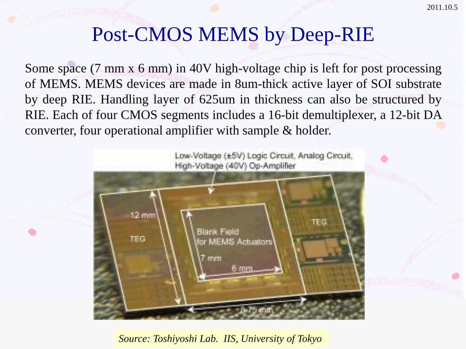
Post-CMOS MEMS by Deep-RIE
Source: Toshiyoshi Lab. IIS, University of Tokyo
Some space (7 mm x 6 mm) in 40V high-voltage chip is left for post processing
of MEMS. MEMS devices are made in 8um-thick active layer of SOI substrate
by deep RIE. Handling layer of 625um in thickness can also be structured by
RIE. Each of four CMOS segments includes a 16-bit demultiplexer, a 12-bit DA
converter, four operational amplifier with sample & holder.
2011.10.5
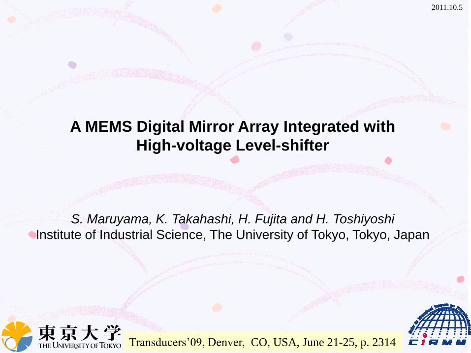
A MEMS Digital Mirror Array Integrated with
High-voltage Level-shifter
S. Maruyama, K. Takahashi, H. Fujita and H. Toshiyoshi
Institute of Industrial Science, The University of Tokyo, Tokyo, Japan
Transducers’09, Denver, CO, USA, June 21-25, p. 2314
2011.10.5
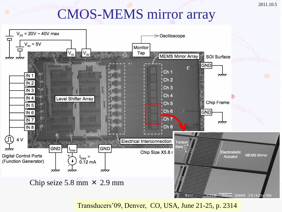
CMOS-MEMS mirror array
Chip seize 5.8 mm × 2.9 mm
Transducers’09, Denver, CO, USA, June 21-25, p. 2314

2011.10.5
Post-CMOS MEMS fabrication
Transducers’09, Denver, CO, USA, June 21-25, p. 2314
2011.10.5
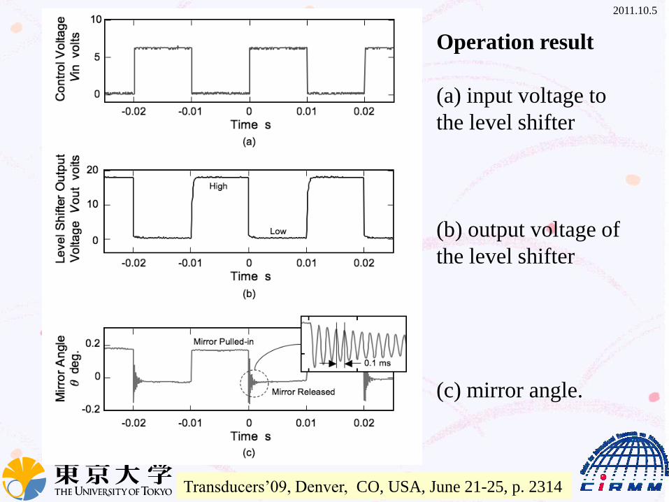
Operation result
(a) input voltage to
the level shifter
(b) output voltage of
the level shifter
(c) mirror angle.
Transducers’09, Denver, CO, USA, June 21-25, p. 2314
2011.10.5
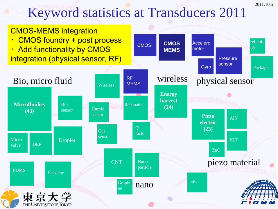
Keyword statistics at Transducers 2011
Microfluidics
(43)
Energy
harvest
(24)
Piezo
electric
(23)
CNT
Parylene
CMOS
MEMS
Pressure
sensor
Droplet
Nano
particle PDMS
Resonator
RF
MEMS
Bio
sensor
Wireless
DEP
CMOS Accelero
meter
Package
Micro
valve
Humid
sensor
Gas
sensor
Q-
factor
AlN
SiC
PZT
Graphe
ne
ZnO
reliabil
ity
Gyro
nano
Bio, micro fluid physical sensor wireless
piezo material
CMOS-MEMS integration
・CMOS foundry + post process
・Add functionality by CMOS
integration (physical sensor, RF)

2011.10.5
High-q, Large-Stopband-Rejection Integrated CMOS-MEMS
Oxide Resonators with Embedded Metal Electrodes
Yu-Chia Liu1, Ming-Han Tsai1, Wen-Chien Chen2, Sheng-Shian Li1,2 and
Weileun Fang1,2
1 Inst. of NanoEngineering and MicroSystems and 2 Dept. of Power Mechanical Engineering
National Tsing Hua University, Hsinchu, Taiwan
Transducers’11, Beijing, China, June 5-9, 2011, p. 934
2011.10.5
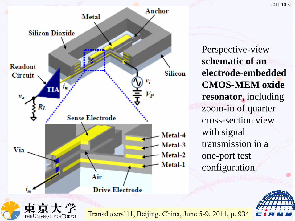
Perspective-view
schematic of an
electrode-embedded
CMOS-MEM oxide
resonator, including
zoom-in of quarter
cross-section view
with signal
transmission in a
one-port test
configuration.
Transducers’11, Beijing, China, June 5-9, 2011, p. 934
2011.10.5
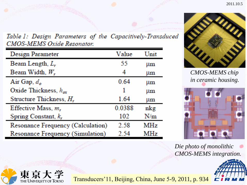
CMOS-MEMS chip
in ceramic housing.
Transducers’11, Beijing, China, June 5-9, 2011, p. 934
Die photo of monolithic
CMOS-MEMS integration.

2011.10.5
Fabrication sequence
(a) a chip manufactured by
standard TSMC 0.35 μm
2P4M process,
(b) metal wet etching to
form resonator structure
and transducer’s gap, and
(c) RIE dry etch to open the
electrode pads.
Transducers’11, Beijing, China,
June 5-9, 2011, p. 934
2011.10.5
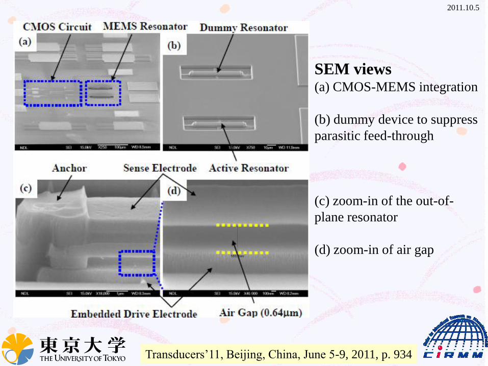
SEM views (a) CMOS-MEMS integration
(b) dummy device to suppress
parasitic feed-through
(c) zoom-in of the out-of-
plane resonator
(d) zoom-in of air gap
Transducers’11, Beijing, China, June 5-9, 2011, p. 934
2011.10.5
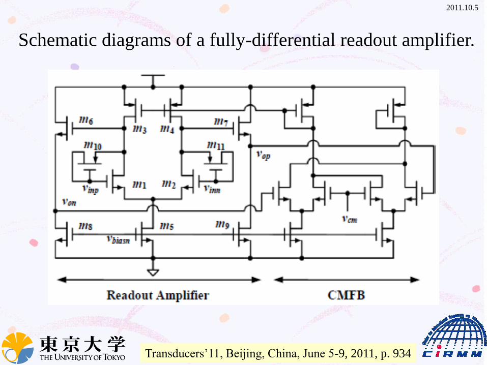
Schematic diagrams of a fully-differential readout amplifier.
Transducers’11, Beijing, China, June 5-9, 2011, p. 934
2011.10.5
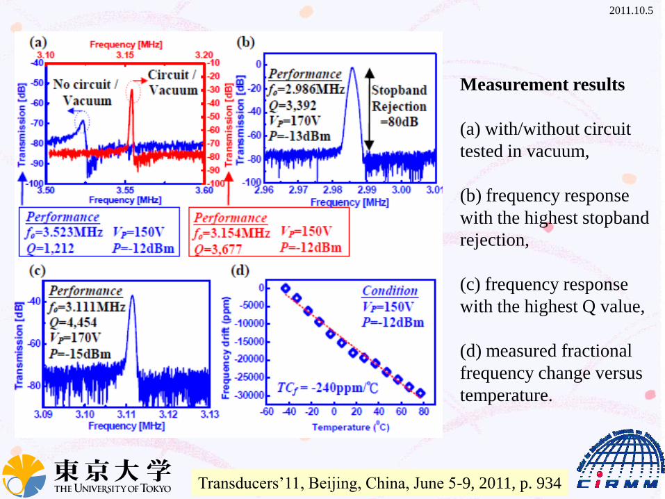
Measurement results
(a) with/without circuit
tested in vacuum,
(b) frequency response
with the highest stopband rejection,
(c) frequency response
with the highest Q value,
(d) measured fractional
frequency change versus
temperature.
Transducers’11, Beijing, China, June 5-9, 2011, p. 934
2011.10.5
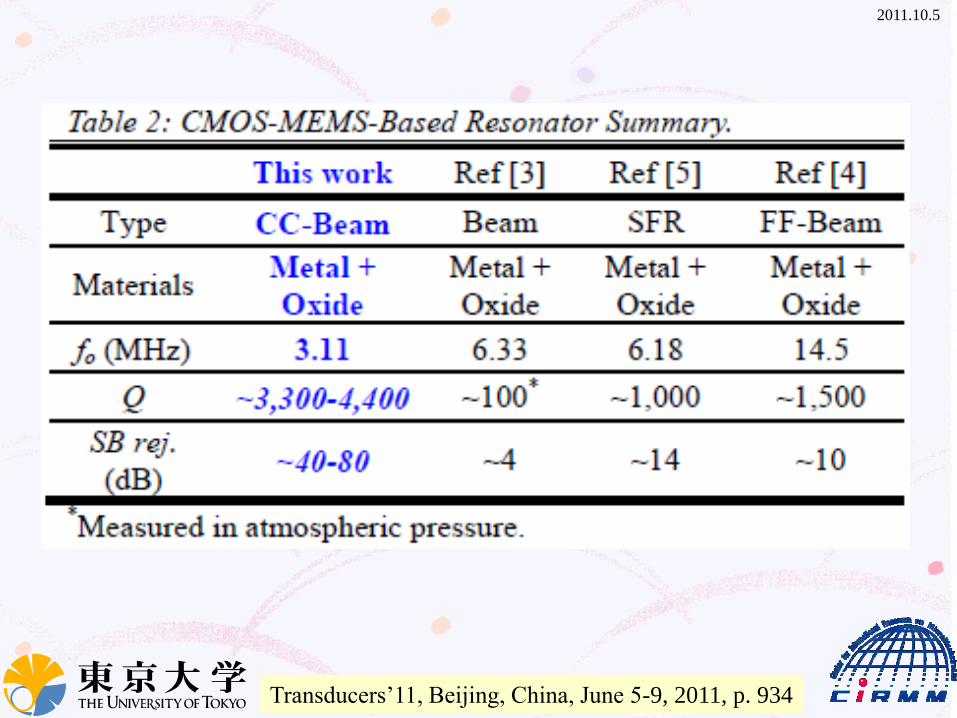
Transducers’11, Beijing, China, June 5-9, 2011, p. 934
2011.10.5
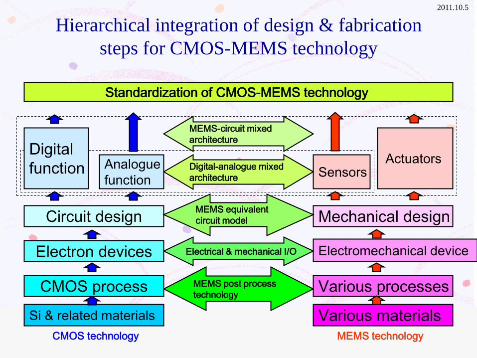
Standardization of CMOS-MEMS technology
Si & related materials
CMOS process
Electron devices
Circuit design
Various materials
Various processes
Electromechanical device
Mechanical design
Sensors Actuators
MEMS post process
technology
Electrical & mechanical I/O
MEMS equivalent
circuit model
Digital-analogue mixed
architecture
Digital
function Analogue
function
CMOS technology MEMS technology
MEMS-circuit mixed
architecture
Hierarchical integration of design & fabrication
steps for CMOS-MEMS technology
2011.10.5
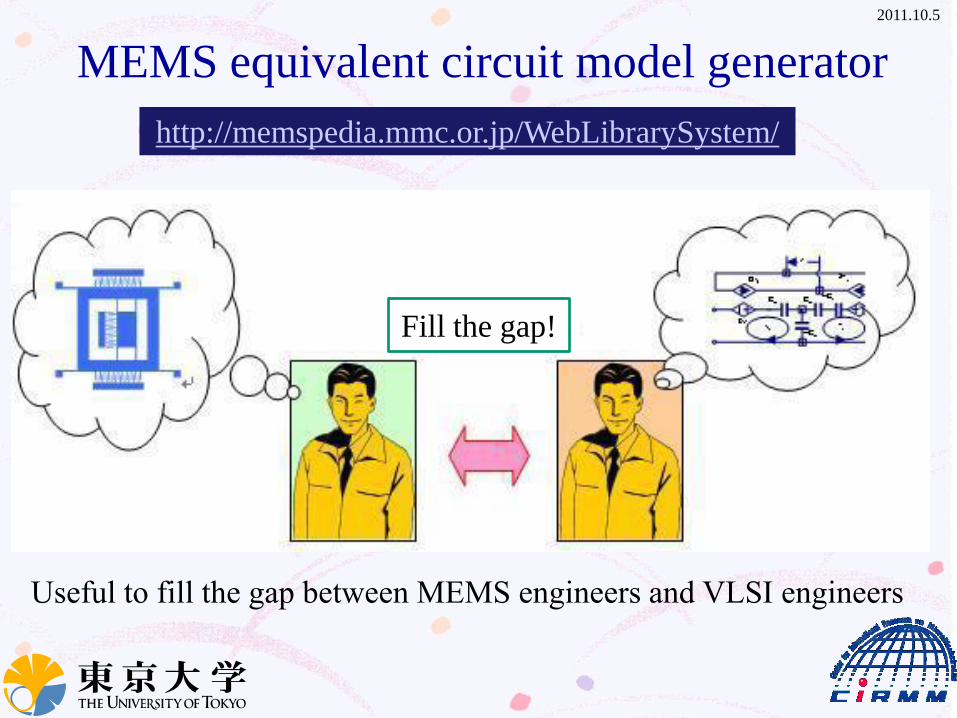
MEMS equivalent circuit model generator
Useful to fill the gap between MEMS engineers and VLSI engineers
Fill the gap!
http://memspedia.mmc.or.jp/WebLibrarySystem/
2011.10.5
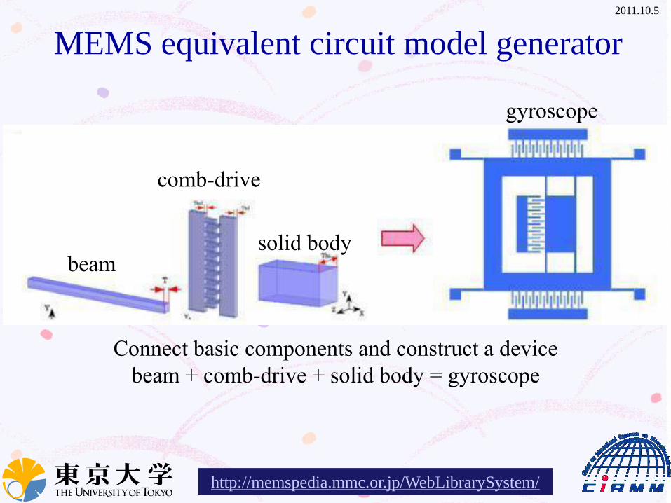
MEMS equivalent circuit model generator
Connect basic components and construct a device
beam + comb-drive + solid body = gyroscope
http://memspedia.mmc.or.jp/WebLibrarySystem/
beam
comb-drive
solid body
gyroscope
2011.10.5
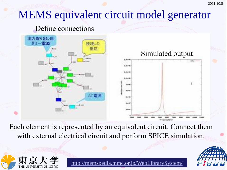
MEMS equivalent circuit model generator
http://memspedia.mmc.or.jp/WebLibrarySystem/
Each element is represented by an equivalent circuit. Connect them
with external electrical circuit and perform SPICE simulation.
Simulated output
Define connections

2011.10.5
Content
• MEMS trend toward MEMS-CMOS
integration
• Examples of MEMS-CMOS integration
• Beyond MEMS-CMOS integration

2011.10.5
1 10 100 1 nm 1 10 100 μm mm
printing
10
weaving
Process integration over the scale
top-down &
bottom-up
integrated
process
bottom-up (building nano
function elements)
top-down (miniaturization
toward nano scale)
nano technology region
self assembly
atom/molecule
handling
self organization molecular
synthesis ultra precision machining
nano lithography
molecular recognition
mechanical assembly bio synthesis
0.1
Large-area
process
nano imprinting
Large-area electronics
2011.10.5
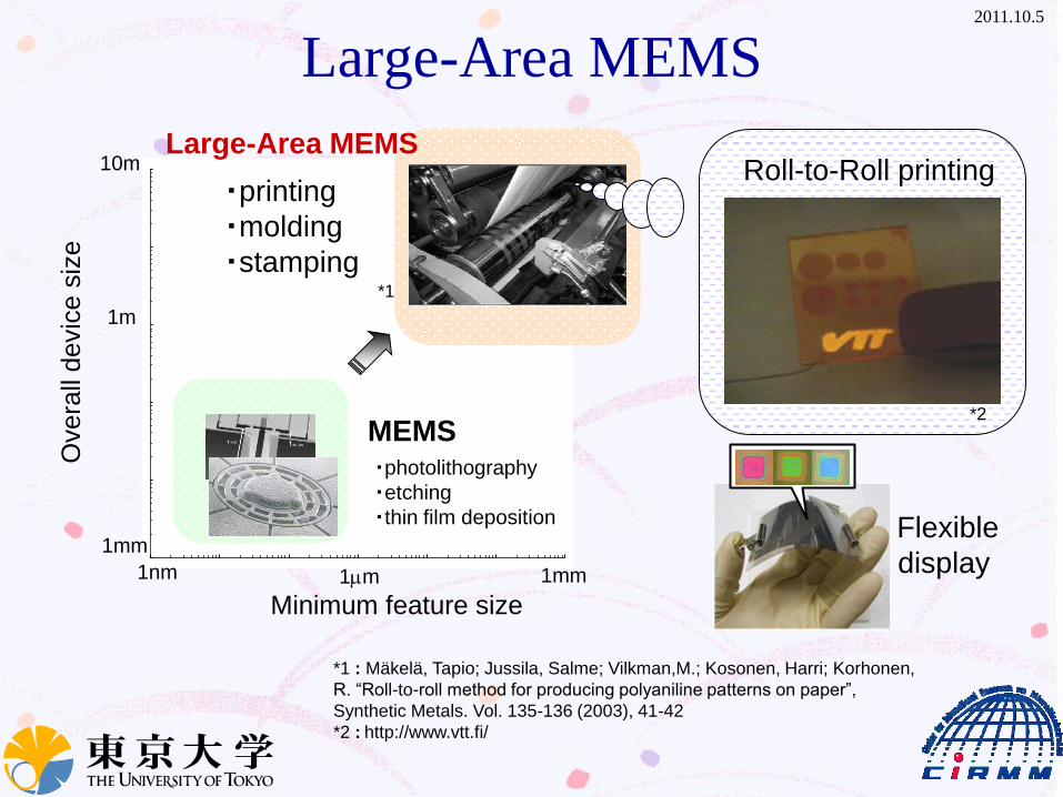
Ove
rall
devic
e s
ize
MEMS ・photolithography
・etching
・thin film deposition
・printing
・molding
・stamping *1
Minimum feature size 1mm 1nm 1mm
1m
1mm
10m
Large-Area MEMS
*1 : Mäkelä, Tapio; Jussila, Salme; Vilkman,M.; Kosonen, Harri; Korhonen,
R. “Roll-to-roll method for producing polyaniline patterns on paper”,
Synthetic Metals. Vol. 135-136 (2003), 41-42
*2 : http://www.vtt.fi/
Roll-to-Roll printing
*2
Large-Area MEMS
Flexible
display
2011.10.5
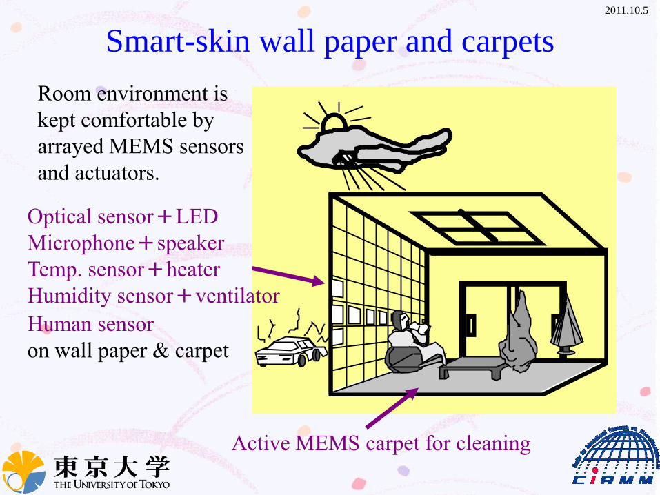
Smart-skin wall paper and carpets
Optical sensor+LED
Microphone+speaker
Temp. sensor+heater
Humidity sensor+ventilator
Human sensor
on wall paper & carpet
Room environment is
kept comfortable by
arrayed MEMS sensors
and actuators.
Active MEMS carpet for cleaning
2011.10.5
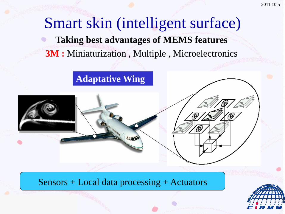
Taking best advantages of MEMS features
3M : Miniaturization , Multiple , Microelectronics
Sensors + Local data processing + Actuators
Adaptative Wing
Smart skin (intelligent surface)
2011.10.5
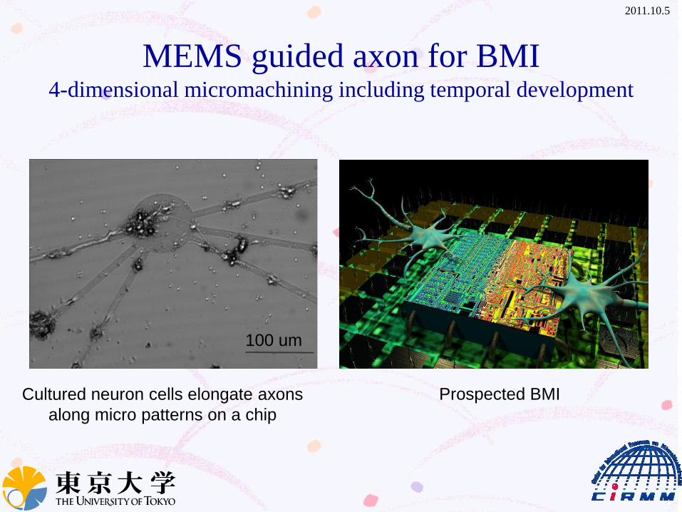
MEMS guided axon for BMI 4-dimensional micromachining including temporal development
Cultured neuron cells elongate axons
along micro patterns on a chip
Prospected BMI
100 um
2011.10.5
Future trends
• Micro/nano machining technology in the future must be the
integration of top-down methods (such as MEMS or VLSI) and
bottom-up methods (such as molecular synthesis and bio
technology).
• Autonomous MEMS instruments to capture ambient
information will be important for security, personal health care,
and environmental protection. Wireless devices and the MEMS
energy source will play key role.
• New fabrication technology for large area integration of
various functional devices will be important. Such products as
flexible/interactive display, MEMS wall paper for lighting/air-
conditioning/noise-reduction, and smart clothes may be produced.
2011.10.5
Conclusion
• MEMS Technology has matured and ready for
CMOS-MEMS integration: More-than-Moore
• Four ways to integrate MEMS and CMOS. Hybrid
integration is most practical. Fully mixed process
and MEMS-first process are suitable to mass
production of many devices. CMOS-first process is
flexible and compatible with existing foundry system.
• Beyond CMOS-MEMS integration, bio/nano objects
will be integrated on chip. Also process for smart
skin will be required.

2011.10.5
Acknowledgment
• METI
• NEDO
• MMC/Beans
laboratory
• COCN
• MEXT
• JSPS
• Global COE Program
• JST
• CNRS (France)
2011.10.5
In collaboration with • Professors affiliated with CIRMM
– Hideki Kawakatsu, Hiroshi Toshiyoshi, Dominique Collard, Teruo Fujii, B. J. Kim, Shoji Takeuchi, Alan Bossebeouf, Takashi Kohno, A.-M. Tixier, Y. Rondelez, Masahiro Nomura
• Prof. Teruyasu Mizoguchi, Prof. Masao Washizu , Prof. T. Yatsui
• Students, post-Docs and visiting scientists – Dr. Momoko Kumemura, Dr. M.C. Tarhan, Dr. C. Bottier, Mr. K.T. Qiu
– Dr. T. Ishida, Dr. L. Jalabert, Mr. T. Sato, Mr. S. Nabeya, Ms. Y. Takayama
• Japanese partners – Prof. Yonezawa (Hokkaido Univ.) and his group
– Prof. Naruo Sasaki (Seikei Univ.) and his group
– Prof. Gen Hashiguchi (Shizuoka Univ.) and his group
– Prof. Ryuji Yokokawa (Kyoto Univ.) and his group
• Global partner – Prof. Fabrizio Cleri (CNRS), Prof. Karl Boehringer (U. Washington),
Prof. S. Karsten (UCLA)
• And many others…


![Lecture 22 (CMOS MEMS part2).ppt [호환 모드]](https://img.dokumen.tips/doc/110x75/623e9f66a5a66f0a8357aee5/lecture-22-cmos-mems-part2ppt-.jpg)