Embed Size (px)
Citation preview

S.Carrara, EPFL Lausanne
(Switzerland)1
Moscow, 12 Moscow, 12 Sept.Sept., 2011, 2011
Memristors: Memristors:
A New Age A New Age
in Electronicsin Electronics
for Sensors for Sensors
and Memoriesand Memories

S.Carrara, EPFL Lausanne
(Switzerland)2
Tutorial OverviewTutorial Overview
� Concepts about Memristors
� Methods to fabricate memristors
� Structures of cross-bars based and
single- wires Memristors
� Measurements on Memristive effects
� Applications to Memories
� Applications to Neural Nets
� Applications to Nano-Bio-sensing

S.Carrara, EPFL - Lausanne
(Switzerland)3
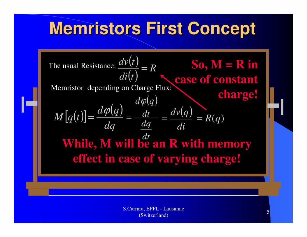
Memristors First ConceptMemristors First Concept
dq
dv
di
dϕ
Four different circuit parameters:
dq
dϕ
)(),(),(),( ttqtitv ϕ
di
dv
The missed equation!
R=
C
1=
L=
M=

S.Carrara, EPFL Lausanne
(Switzerland)4
The Memristor requestThe Memristor request
Symmetry reasons seem demanding for Memristors
S.Carrara, EPFL - Lausanne
(Switzerland)5
Memristors First ConceptMemristors First Concept
So, M = R in
case of constant
charge!
( )[ ]( )
dq
qdtqM
ϕ=
( )( )
Rtdi
tdv=
( )
dt
dqdt
qdϕ
=
Memristor depending on Charge Flux:
The usual Resistance:
( )di
qdv=
While, M will be an R with memory
effect in case of varying charge!
)(qR=

S.Carrara, EPFL Lausanne
(Switzerland)6
The NameThe Name
Memory
Resistor
MEMRISTOR

S.Carrara, EPFL Lausanne
(Switzerland)7
Memristor with lateral injectionMemristor with lateral injection
Carriers are injected by the source side
S D

S.Carrara, EPFL Lausanne
(Switzerland)8
A two-terminals Memristor may be modeled by through two resistors as an element which vary the
resistance upon the applied voltage
Possible Memristor ModelPossible Memristor Model

S.Carrara, EPFL - Lausanne
(Switzerland)9
Memristors First ConceptMemristors First Concept
( ) )()(
1)(
tiD
twR
D
twRtv OFFON
−+=
)()(
tiD
R
dt
tdw ONVµ=
−= )(1)(
2tq
D
RRqM ONV
OFF
µ
)()( tqD
Rtw ON
Vµ=
More evident at nano-scale!

S.Carrara, EPFL Lausanne
(Switzerland)10
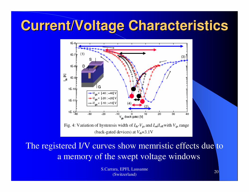
Current/Voltage CharacteristicsCurrent/Voltage Characteristics
Memristic effects are observable in I-V curves
as a memory of the channel doping in time

S.Carrara, EPFL Lausanne
(Switzerland)11
How to build a Memristor?How to build a Memristor?
“These results serve as the foundation for
understanding a wide range of hysteretic
current-voltage behavior observed in many
nano-scale electronic devices”
“[…] until now no one has presented either a
useful physical model or an example of a
memristor”

S.Carrara, EPFL Lausanne
(Switzerland)12
Pt/TiOPt/TiO22--xx/TiO/TiO22/Pt memristors/Pt memristors
12
Source: Yang et al, Nature Nanotechnology 2008
O-v i

S.Carrara, EPFL Lausanne
(Switzerland)13
Memristors by organicMemristors by organic
Carrier may be injected by the top polymer
S D

S.Carrara, EPFL Lausanne
(Switzerland)14
Organic MemristorOrganic Memristor
14
Source: Berzina et al, Applied Materials & Interfaces 2009
Li or Rb+v i

S.Carrara, EPFL Lausanne
(Switzerland)15
Memristors in polyMemristors in poly--SiliconSilicon
Thursday, September 22, 2011 15
Source: Ben-Jamaa, Carrara et al., IEEE Nano 2009

S.Carrara, EPFL Lausanne
(Switzerland)16
Sizes OverviewSizes Overview
Insulator
(SiO2)
Poly-Si
spacer
Si substrate
• Dimensions are
not true to scale!
• Only frontend
processing is
depicted
• Backend includes
passivation +
metallization
~ 400 nm~ 400 nm
~ 70 nm
~ 70 nm~ 20 nm

S.Carrara, EPFL Lausanne
(Switzerland)17
Fabrication ResultsFabrication Results
The SEM imaging shows the quality of poly-silicon wires fabricated by using spacers technique

S.Carrara, EPFL Lausanne
(Switzerland)18
The registered I/V curves show memristic effects due to
a memory of the swept voltage windows
Current/Voltage CharacteristicsCurrent/Voltage Characteristics
Electrons de-trapping
Electrons trapping
Holes trapping
Holes de-trapping

S.Carrara, EPFL Lausanne
(Switzerland)19
Conductivity MechanismsConductivity Mechanisms
Both electrons and holes based conductivity is affected by Memristor effect
S.Carrara, EPFL Lausanne
(Switzerland)20
The registered I/V curves show memristic effects due to
a memory of the swept voltage windows
Current/Voltage CharacteristicsCurrent/Voltage Characteristics

S.Carrara, EPFL - Lausanne
(Switzerland)21
)()()()()( EgEgEgEgEg GDGATDTA +++=
TD
v
W
EE
TDTD eNEg
−
=)(
2
)(
−−
= GA
GA
W
EE
GAGA eNEg
2
)(
−−
= GD
GD
W
EE
GDGA eNEg
TA
c
W
EE
TATA eNEg
−
=)(
Tail States Gaussian StatesAcceptors State
Donors State
Simulations by Simulations by
driftdrift--diffusion modeldiffusion model

S.Carrara, EPFL Lausanne
(Switzerland)22
2D Simulations by Atlas follow the experimental
data accounting for negative trapped charges at the
Poly-Si/SiO2 interface
-20 -10 0 10 20
10-11
10-10
10-9
10-8
10-7
Simulation
Dra
in C
urr
en
t (
A)
Gate Voltage (V)
Experiment
Simulations ResultSimulations Result

S.Carrara, EPFL Lausanne
(Switzerland)23
Memristors by BulkMemristors by Bulk--Silicon, tooSilicon, too
Thursday, September 22, 2011 23

S.Carrara, EPFL Lausanne
(Switzerland)24
Memristors by CrystallineMemristors by Crystalline--SiliconSilicon
24
Source: D.Sacchetto, .., Carrara, et al., IEEE ISCAS 2010

S.Carrara, EPFL Lausanne
(Switzerland)25
Silicon NanowiresSilicon Nanowires
25
Polysilicon
Gate All
Around
c-Si nanowire
channel
S.Carrara, EPFL Lausanne
(Switzerland)26
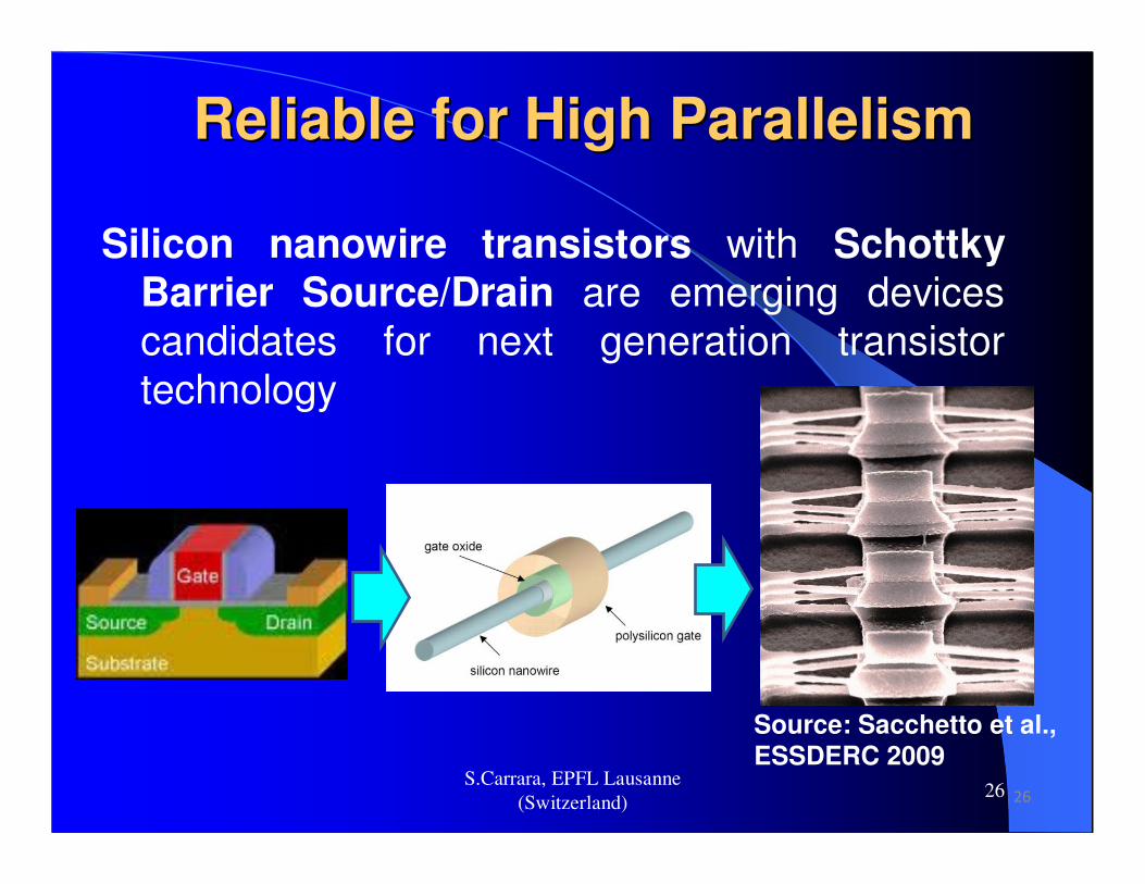
Reliable for High ParallelismReliable for High Parallelism
Silicon nanowire transistors with Schottky Barrier Source/Drain are emerging devices candidates for next generation transistor technology
26
Source: Sacchetto et al., ESSDERC 2009

S.Carrara, EPFL Lausanne
(Switzerland)27
Memristive BehaviorMemristive Behavior
27
V0(Vds)
Vds Ids
Vgs and t are
constants
Vds as the
input
x80
c-SiNW : Ids-Vds

S.Carrara, EPFL Lausanne
(Switzerland)28
Hysteretic Charge TrappingHysteretic Charge Trapping
Thursday, September 22, 2011 28
c-SiNW : Sweep frequency dependence
V0(Vgs,
t)
Vgs
t
Ids
Vds as the
constant
Vgs and t as the
input
t

S.Carrara, EPFL Lausanne
(Switzerland)29
Theory of Operation (1)Theory of Operation (1)
Thursday, September 22, 2011 29
e- h+
constant Vds
Vgs polarity
selects the
type of carrier
S SD D
e-/h+v i

S.Carrara, EPFL Lausanne
(Switzerland)30
Theory of Operation (2)Theory of Operation (2)
Thursday, September 22, 2011 30
( )1/))((/ 0 −⋅=
−− kTVVVkT
sdsdsB eeII
φ
Schottky Barrier height
Schottky barrier built-in voltage
),,()( 00 tVVVVV gsds=
Ids
S D

S.Carrara, EPFL Lausanne
(Switzerland)31
Theory of Operation (2)Theory of Operation (2)
Thursday, September 22, 2011 31
V0(Vds,Vgs,t)
Vgs
Vds
t
Ids
INP
UT
S
STATE
variable
OUTPUT

S.Carrara, EPFL Lausanne
(Switzerland)32
Theory of Operation (2)Theory of Operation (2)
Simplification of model-w structure

S.Carrara, EPFL Lausanne
(Switzerland)33
Theory of Operation (2)Theory of Operation (2)
Model-w equivalent circuit

S.Carrara, EPFL - Lausanne
(Switzerland)34
Theory of Operation (2)Theory of Operation (2)
∫=⇒ dttVL
aw )(
µ
[ ]btaL
w +=⇒ )(ϕµ
Eadt
dwµ=
L
tVa
)(µ=

S.Carrara, EPFL - Lausanne
(Switzerland)35
Theory of Operation (2)Theory of Operation (2)
VVV rl γ=−
0)(1 =
−−+− ti
L
wRVVV sirl
That’s the Kirchoff’s Voltage Law

S.Carrara, EPFL - Lausanne
(Switzerland)36
Theory of Operation (2)Theory of Operation (2)
0)(1 =
−−− ti
L
wRVV SIγ
That’s the Kirchoff’s Voltage Law
)(
1
)1(ti
L
wR
V
SI
=
−
−γ)()()( tVGti ϕ=⇒

S.Carrara, EPFL Lausanne
(Switzerland)37
Theory of Operation (2)Theory of Operation (2)
Comparison of model-w with measurements

S.Carrara, EPFL Lausanne
(Switzerland)38
Theory of Operation (2)Theory of Operation (2)
State variable after addition of phase parameter

S.Carrara, EPFL Lausanne
(Switzerland)39
Theory of Operation (3)Theory of Operation (3)
Equivalent Circuit Model

S.Carrara, EPFL Lausanne
(Switzerland)40
Theory of Operation (3)Theory of Operation (3)
Explanation of circuit operation

S.Carrara, EPFL Lausanne
(Switzerland)41
Theory of Operation (3)Theory of Operation (3)
Equivalent Circuit Model vs measurements

S.Carrara, EPFL Lausanne
(Switzerland)42
Applications to MemoryApplications to Memory
Monolithic 3D integration of state-of-the-art transistor technologies with memristive devices, with opportunities for high-density 3D crossbar
construction:
� Multi-level Resistive RAMs
� Dynamic RAMs
42
GATE
lines
CHANNEL lines

S.Carrara, EPFL Lausanne
(Switzerland)43
Crossbar Memristors for (RRAM)
resistive random-access-memory (RRAM) from hysteretic resistive memristive devices

S.Carrara, EPFL Lausanne
(Switzerland)44
Crossbar Memristors for (RRAM)Crossbar Memristors for (RRAM)

S.Carrara, EPFL Lausanne
(Switzerland)45
Memristive Programmable Devices by Through Silicon Vias
Concept image of planar Re-RAM made of Pt/TiO2/Pt stack

S.Carrara, EPFL Lausanne
(Switzerland)46
Memristive Programmable Devices by Through Silicon Vias
Reconstructed 3D photograph of the TSV −Cu/TiO2/Pt device stack.

S.Carrara, EPFL Lausanne
(Switzerland)47
Memristive Programmable Devices by Through Silicon Vias
Resistive switching through I − V sweeps for planar Pt/TiO2/Pt

S.Carrara, EPFL Lausanne
(Switzerland)48
Resistive switching through I − V sweeps using TSV
− Cu/TiO2/Pt programmable fuse
Memristive Programmable Memristive Programmable
Devices by Through Silicon Devices by Through Silicon ViasVias

S.Carrara, EPFL Lausanne
(Switzerland)49
Resistive switching through I − V sweeps using TSV − Pt/TiO2/Pt programmable fuse
Memristive Programmable Memristive Programmable
Devices by Through Silicon Devices by Through Silicon ViasVias

S.Carrara, EPFL Lausanne
(Switzerland)50
Applications to NeuralApplications to Neural--NetsNets
Nanoscale Memristor Device as Synapse in Neuromorphic Systems

S.Carrara, EPFL Lausanne
(Switzerland)51
Applications to NeuralApplications to Neural--NetsNets
The change in current in sequential voltage sweeps
The The
LearningLearning

S.Carrara, EPFL Lausanne
(Switzerland)52
Applications to NeuralApplications to Neural--NetsNets
Neural Nets by organic materials as well

S.Carrara, EPFL Lausanne
(Switzerland)53
Homo- (a) and hetero- (b)
Synaptic junctionsModel of learning for Limnea
Stagnalis: association of the
mechanical stimulus with presence of
food
Neural Network of a Snail
SYNAPSES

S.Carrara, EPFL Lausanne
(Switzerland)54
Input 1 – mechanical (neutral) stimulus
Input 2 – presence of food
Output: current as a result of the presence
of the neutral stimulus only
Training: application of both stimuli
Organic
memristive device
–synapse analog
V. Erokhin et al., BioNanoScience, 1, 24-30 (2011)
Neural Network of a Snail

S.Carrara, EPFL Lausanne
(Switzerland)55
Measure of the Carriers Measure of the Carriers
injectioninjection
The Li+ ions normally used to dope PEO were not
adequate for such measurements because their fluorescent
energy cannot be detected at atmospheric conditions.
Thus, the heavier Rb ions were used

S.Carrara, EPFL Lausanne
(Switzerland)56
Measure of the Carriers Measure of the Carriers
injectioninjection
Grazing-incidence X-ray fluorescence measurements were applied for a time-resolved study of an organic memristor conductivity variation
mechanism

S.Carrara, EPFL Lausanne
(Switzerland)57
Applications to BioApplications to Bio--SensingSensing
Frontend Passivation
BackendFunctionalization
Definition of Silicon
nanowire
Isolation of devices,
via opening for
metalization and
functionalization
Metalization: NiCr
or Cr/NiCr or Al
Grafting of bio-
probes

S.Carrara, EPFL Lausanne
(Switzerland)58
pH Dependent SensorpH Dependent Sensor� pH Sensor obtained by modifying Si oxide surface with 3-
aminopropyltriethoxysilane yielding amino and silanol groups (acting as receptors) at surface
Patolsky et al., Nanowire-Based Biosensors, Analytical Chemistry, 2006, 4261-4269
Protonation/deprotonation altered charge density at surface thereby changing conductance

S.Carrara, EPFL Lausanne
(Switzerland)59
Detecting Single VirusDetecting Single Virus� When virus binds to antibody receptor, conductance changes from
baseline value
� When it unbinds, conductance returns to baseline value
Patolsky et al., Nanowire-Based Biosensors, Analytical Chemistry, 2006, 4261-4269
Ultra-dense NW device where minimum scale is set by
size of virus
S.Carrara, EPFL Lausanne
(Switzerland)60
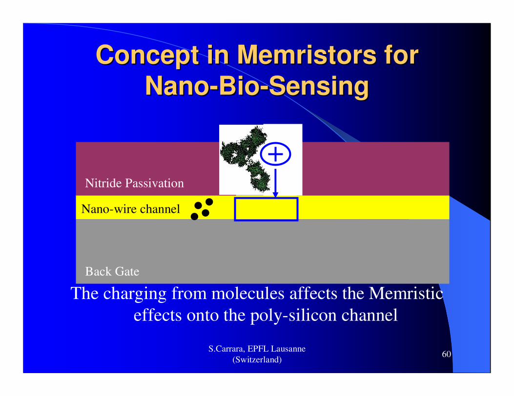
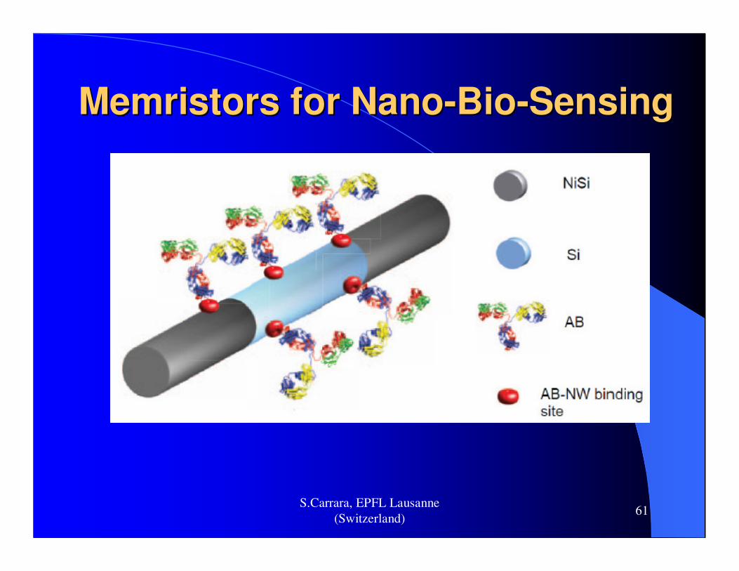
Concept in Memristors forConcept in Memristors for
NanoNano--BioBio--SensingSensing
The charging from molecules affects the Memristic
effects onto the poly-silicon channel
Back Gate
Nitride Passivation
Nano-wire channel
Top-gate
S.Carrara, EPFL Lausanne
(Switzerland)61
Memristors for NanoMemristors for Nano--BioBio--SensingSensing

S.Carrara, EPFL Lausanne
(Switzerland)62
Suspended Si ribbon with 600nm trench dimension before sacrificial oxidation
Memristors for NanoMemristors for Nano--BioBio--SensingSensing

S.Carrara, EPFL Lausanne
(Switzerland)63
Suspended Si nanowire with 100nm diameter and hard mask
opened at contact regions before Ni/Ti metal deposition
Memristors for NanoMemristors for Nano--BioBio--SensingSensing

S.Carrara, EPFL Lausanne
(Switzerland)64
14.8nm14.8nm
12.8nm12.8nm
9.3 nm9.3 nm
The size of an AntibodyThe size of an Antibody

S.Carrara, EPFL Lausanne
(Switzerland)65
Bio affects MemconductanceBio affects Memconductance
Ids − Vds curves taken (1) before and (2) after
memristive-biosensors functionalization
Minima Minima
VoltageVoltage
GapGap

S.Carrara, EPFL Lausanne
(Switzerland)66
Bio affects MemconductanceBio affects Memconductance
Ids − Vds curves: before and after the up-take of 5 pM AG solution.

S.Carrara, EPFL Lausanne
(Switzerland)67
The charges of an Antibody?The charges of an Antibody?
The crystallographic structure of an antibody

S.Carrara, EPFL Lausanne
(Switzerland)68
Charged ResiduesCharged ResiduesPositively Charged
Arginine
+
Histidine
+
Lysine
+
Polar Uncharged
-
Aspartic Acid
-
Glutamic Acid
Neg. Charged
-
-
+
+
Serine
-
+
Threonine
-
+
Aspargine
-
+
Glutamine
-
+
-
+
-
+ +
-

S.Carrara, EPFL Lausanne
(Switzerland)69
The charges of an AntibodyThe charges of an Antibody
The crystallographic structure of an antibody

S.Carrara, EPFL Lausanne
(Switzerland)70
• Memristors are devices with a memory of its bias story
• Memristic effect has been registered in I/V characteristics with both organic and inorganic materials, including Silicon
• 2D simulations and Fluorescent Measurements confirmed that Memristic effects are due to charges trapping in the Channel
• Applications of memristic devices are feasible for Memories, biomorphic networks, and Biosensors
• Nano-electronics is now at the beginning of a new age thanks to the exploitation of Memristors
ConclusionsConclusions

(c) S.Carrara, EPFL - Lausanne
(Switzerland)71
Thanks to:Thanks to:
� Davide Sacchetto
� Haykel Ben Jamaa
� Marie-Agnès Doucey
� Akshat Dave
� Pietro Dalmastro
� Julius Georgiou
� Victor Erokhin
� Yusuf Leblebici
� Giovanni De Micheli

S.Carrara, EPFL Lausanne
(Switzerland)72
Coordinates:Dr. Sandro Carrara Ph.D
Integrated Laboratory Systems
Swiss Federal Institute of Technology (EPFL)
CH-1015 Lausanne
Web: http://si2.epfl.ch/~scarrara/
email: [email protected]
Thank you for your attention!Thank you for your attention!