Embed Size (px)
Citation preview
MELSEC iQ-F
FX5 User's Manual (Application)

1
SAFETY PRECAUTIONS(Read these precautions before use.)
Before using this product, please read this manual and the relevant manuals introduced in this manual carefully and pay
attention to safety in order to handle the product correctly.
This manual classifies the safety precautions into two categories: [ WARNING] and [ CAUTION].
Depending on the circumstances, procedures indicated by [ CAUTION] may also cause severe injury.
It is important to follow all precautions for personal safety.
Store this manual in a safe place so that it can be read whenever necessary. Always forward it to the end user.
[DESIGN PRECAUTIONS]
WARNING● Make sure to set up the following safety circuits outside the PLC to ensure safe system operation
even during external power supply problems or PLC failure. Otherwise, malfunctions may cause
serious accidents.
- Most importantly, set up the following: an emergency stop circuit, a protection circuit, an interlock
circuit for opposite movements (such as forward vs. reverse rotation), and an interlock circuit to
prevent damage to the equipment at the upper and lower positioning limits.
- Note that when the CPU module detects an error, such as a watchdog timer error, during self-
diagnosis, all outputs are turned off. Also, when an error that cannot be detected by the CPU
module occurs in an input/output control block, output control may be disabled. External circuits
and mechanisms should be designed to ensure safe machine operation in such a case.
- Note that the output current of the 24 V DC service power supply varies depending on the model
and the absence/presence of extension modules. If an overload occurs, the voltage automatically
drops, inputs in the PLC are disabled, and all outputs are turned off. External circuits and
mechanisms should be designed to ensure safe machine operation in such a case.
- Note that when an error occurs in a relay or transistor of an output circuit, the output might stay on
or off. For output signals that may lead to serious accidents, external circuits and mechanisms
should be designed to ensure safe machine operation.
● Construct an interlock circuit in the program to ensure safe operation for the whole system when
executing control (for data change) of the PLC in operation.
Read the manual thoroughly and ensure complete safety before executing other controls (for program
change, parameter change, forced output and operation status change) of the PLC in operation.
Otherwise, the machine may be damaged and accidents may occur due to erroneous operations.
● In an output circuit, when a load current exceeding the current rating or an overcurrent caused by a
load short-circuit flows for a long time, it may cause smoke and fire. To prevent this, configure an
external safety circuit, such as a fuse.
● For the operating status of each station after a communication failure of the network, refer to relevant
manuals for the network. Incorrect output or malfunction may result in an accident.
WARNINGIndicates that incorrect handling may cause hazardous conditions, resulting in
death or severe injury.
CAUTIONIndicates that incorrect handling may cause hazardous conditions, resulting in
minor or moderate injury or property damage.
2
[DESIGN PRECAUTIONS]
[INSTALLATION PRECAUTIONS]
[WIRING PRECAUTIONS]
CAUTION● After the CPU module is powered on or is reset, the time taken to enter the RUN status varies
depending on the system configuration, parameter settings, and/or program size.
Design circuits so that the entire system will always operate safely, regardless of this variation in time.
CAUTION● Connect the expansion board and expansion adapter securely to their designated connectors. Loose
connections may cause malfunctions.
● Connect the extension cables, peripheral device cables, input/output cables and battery connecting
cable securely to their designated connectors. Loose connections may cause malfunctions.
● When using an SD memory card, insert it into the SD memory card slot. Check that it is inserted
completely. Poor contact may cause malfunction.
● Turn off the power to the PLC before attaching or detaching the following devices. Failure to do so
may cause device failures or malfunctions.
- Peripheral devices, expansion board and expansion adapter
- Extension modules, bus conversion module and connector conversion module
- Battery
CAUTION● Do not bundle the power line, control line and communication cables together with or lay them close to
the main circuit, high-voltage line, load line or power line. As a guideline, lay the power line, control
line and connection cables at least 100 mm (3.94") away from the main circuit, high-voltage line, load
line or power line. Noise may cause malfunctions.
3
[STARTUP AND MAINTENANCE PRECAUTIONS]
[PRECAUTIONS IN OPERATION]
WARNING● Do not touch any terminal while the PLC's power is on. Doing so may cause electric shock or
malfunctions.
● Before modifying the program in mid-operation, forcing output, running or stopping the PLC, read this
manual and the associated manuals carefully and ensure complete safety. An operation error may
damage the machinery or cause accidents.
● Do not change the program in the PLC from two or more peripheral equipment devices (such as an
engineering tool and a GOT) at the same time. Doing so may cause destruction or malfunction of the
PLC program.
● Use the battery for memory backup in conformance to the FX5 User's Manual (Hardware).
- Use the battery for the specified purpose only.
- Connect the battery correctly.
- Do not charge, disassemble, heat, put in fire, short-circuit, connect reversely, weld, swallow or
burn the battery, or apply excessive force (vibration, impact, drop, etc.) to the battery.
- Do not store or use the battery at high temperatures or expose to direct sunlight.
- Do not expose to water, bring near fire or touch liquid leakage or other contents directly.
Incorrect handling of the battery may cause excessive heat, bursting, ignition, liquid leakage or
deformation, and lead to injury, fire or failures and malfunction of facilities and other equipment.
CAUTION● Construct an interlock circuit in the program to ensure safe operation for the whole system when
executing control (for data change) of the PLC in operation. Read the manual thoroughly and ensure
complete safety before executing other controls (for program change, parameter change, forced
output and operation status change) to the PLC in operation. Otherwise, the machine may be
damaged and accidents may occur by erroneous operations.
4
INTRODUCTIONThis manual contains text, diagrams and explanations which will guide the reader in the correct installation, safe use and
operation of the FX5 Programmable Controllers and should be read and understood before attempting to install or use the
module.
Always forward it to the end user.
Regarding use of this product
� This product has been manufactured as a general-purpose part for general industries, and has not been designed or
manufactured to be incorporated in a device or system used in purposes related to human life.
� Before using the product for special purposes such as nuclear power, electric power, aerospace, medicine or passenger
movement vehicles, consult Mitsubishi Electric.
� This product has been manufactured under strict quality control. However when installing the product where major
accidents or losses could occur if the product fails, install appropriate backup or failsafe functions in the system.
Note
� If in doubt at any stage during the installation of the product, always consult a professional electrical engineer who is
qualified and trained in the local and national standards. If in doubt about the operation or use, please consult the nearest
Mitsubishi Electric representative.
� Since the examples indicated by this manual, technical bulletin, catalog, etc. are used as a reference, please use it after
confirming the function and safety of the equipment and system. Mitsubishi Electric will accept no responsibility for actual
use of the product based on these illustrative examples.
� This manual content, specification etc. may be changed without a notice for improvement.
� The information in this manual has been carefully checked and is believed to be accurate; however, if you notice a doubtful
point, an error, etc., please contact the nearest Mitsubishi Electric representative. When doing so, please provide the
manual number given at the end of this manual.

5
MEMO
6
CONTENTSSAFETY PRECAUTIONS . . . . . . . . . . . . . . . . . . . . . . . . . . . . . . . . . . . . . . . . . . . . . . . . . . . . . . . . . . . . . . . . . . . .1
INTRODUCTION. . . . . . . . . . . . . . . . . . . . . . . . . . . . . . . . . . . . . . . . . . . . . . . . . . . . . . . . . . . . . . . . . . . . . . . . . . .4
RELEVANT MANUALS . . . . . . . . . . . . . . . . . . . . . . . . . . . . . . . . . . . . . . . . . . . . . . . . . . . . . . . . . . . . . . . . . . . . .12
TERMS . . . . . . . . . . . . . . . . . . . . . . . . . . . . . . . . . . . . . . . . . . . . . . . . . . . . . . . . . . . . . . . . . . . . . . . . . . . . . . . . .12
PART 1 PROGRAMMING
CHAPTER 1 PROGRAM EXECUTION 16
1.1 Scan Configuration . . . . . . . . . . . . . . . . . . . . . . . . . . . . . . . . . . . . . . . . . . . . . . . . . . . . . . . . . . . . . . . . . . . . . . 16
Initial processing and initialization processing in RUN mode . . . . . . . . . . . . . . . . . . . . . . . . . . . . . . . . . . . . . . . 16
I/O refresh . . . . . . . . . . . . . . . . . . . . . . . . . . . . . . . . . . . . . . . . . . . . . . . . . . . . . . . . . . . . . . . . . . . . . . . . . . . . . . 17
Program operations . . . . . . . . . . . . . . . . . . . . . . . . . . . . . . . . . . . . . . . . . . . . . . . . . . . . . . . . . . . . . . . . . . . . . . . 17
END processing. . . . . . . . . . . . . . . . . . . . . . . . . . . . . . . . . . . . . . . . . . . . . . . . . . . . . . . . . . . . . . . . . . . . . . . . . . 17
1.2 Scan Time. . . . . . . . . . . . . . . . . . . . . . . . . . . . . . . . . . . . . . . . . . . . . . . . . . . . . . . . . . . . . . . . . . . . . . . . . . . . . . 18
Initial scan time . . . . . . . . . . . . . . . . . . . . . . . . . . . . . . . . . . . . . . . . . . . . . . . . . . . . . . . . . . . . . . . . . . . . . . . . . . 18
1.3 Program Execution Sequence . . . . . . . . . . . . . . . . . . . . . . . . . . . . . . . . . . . . . . . . . . . . . . . . . . . . . . . . . . . . . 19
1.4 Execution Type of Program . . . . . . . . . . . . . . . . . . . . . . . . . . . . . . . . . . . . . . . . . . . . . . . . . . . . . . . . . . . . . . . 20
Initial execution type program . . . . . . . . . . . . . . . . . . . . . . . . . . . . . . . . . . . . . . . . . . . . . . . . . . . . . . . . . . . . . . . 20
Scan execution type program . . . . . . . . . . . . . . . . . . . . . . . . . . . . . . . . . . . . . . . . . . . . . . . . . . . . . . . . . . . . . . . 21
Fixed scan execution type program. . . . . . . . . . . . . . . . . . . . . . . . . . . . . . . . . . . . . . . . . . . . . . . . . . . . . . . . . . . 21
Event execution type program. . . . . . . . . . . . . . . . . . . . . . . . . . . . . . . . . . . . . . . . . . . . . . . . . . . . . . . . . . . . . . . 25
Stand-by type program . . . . . . . . . . . . . . . . . . . . . . . . . . . . . . . . . . . . . . . . . . . . . . . . . . . . . . . . . . . . . . . . . . . . 28
1.5 Program Type. . . . . . . . . . . . . . . . . . . . . . . . . . . . . . . . . . . . . . . . . . . . . . . . . . . . . . . . . . . . . . . . . . . . . . . . . . . 29
Subroutine program. . . . . . . . . . . . . . . . . . . . . . . . . . . . . . . . . . . . . . . . . . . . . . . . . . . . . . . . . . . . . . . . . . . . . . . 29
Interrupt program. . . . . . . . . . . . . . . . . . . . . . . . . . . . . . . . . . . . . . . . . . . . . . . . . . . . . . . . . . . . . . . . . . . . . . . . . 30
CHAPTER 2 PROCESSING OF OPERATIONS ACCORDING TO CPU MODULE
OPERATION STATUS 35
CHAPTER 3 CPU MODULE MEMORY CONFIGURATION 37
3.1 Memory Configuration . . . . . . . . . . . . . . . . . . . . . . . . . . . . . . . . . . . . . . . . . . . . . . . . . . . . . . . . . . . . . . . . . . . 37
Memory configuration . . . . . . . . . . . . . . . . . . . . . . . . . . . . . . . . . . . . . . . . . . . . . . . . . . . . . . . . . . . . . . . . . . . . . 37
3.2 Files . . . . . . . . . . . . . . . . . . . . . . . . . . . . . . . . . . . . . . . . . . . . . . . . . . . . . . . . . . . . . . . . . . . . . . . . . . . . . . . . . . 39
File type and storage destination memory. . . . . . . . . . . . . . . . . . . . . . . . . . . . . . . . . . . . . . . . . . . . . . . . . . . . . . 39
Executable file operations . . . . . . . . . . . . . . . . . . . . . . . . . . . . . . . . . . . . . . . . . . . . . . . . . . . . . . . . . . . . . . . . . . 39
PART 2 FUNCTIONS
CHAPTER 4 FUNCTION LIST 42
CHAPTER 5 SCAN MONITORING FUNCTION 44
5.1 Scan time monitoring time setting. . . . . . . . . . . . . . . . . . . . . . . . . . . . . . . . . . . . . . . . . . . . . . . . . . . . . . . . . . 44
5.2 Resetting of the watchdog timer . . . . . . . . . . . . . . . . . . . . . . . . . . . . . . . . . . . . . . . . . . . . . . . . . . . . . . . . . . . 44
5.3 Precautions . . . . . . . . . . . . . . . . . . . . . . . . . . . . . . . . . . . . . . . . . . . . . . . . . . . . . . . . . . . . . . . . . . . . . . . . . . . . 44
Watchdog timer reset when executing a program repeatedly . . . . . . . . . . . . . . . . . . . . . . . . . . . . . . . . . . . . . . . 44
Scan time when the WDT instruction is used . . . . . . . . . . . . . . . . . . . . . . . . . . . . . . . . . . . . . . . . . . . . . . . . . . . 45
7
CO
NT
EN
TS
CHAPTER 6 CLOCK FUNCTION 46
6.1 Time Setting . . . . . . . . . . . . . . . . . . . . . . . . . . . . . . . . . . . . . . . . . . . . . . . . . . . . . . . . . . . . . . . . . . . . . . . . . . . . 46
Clock data . . . . . . . . . . . . . . . . . . . . . . . . . . . . . . . . . . . . . . . . . . . . . . . . . . . . . . . . . . . . . . . . . . . . . . . . . . . . . . 46
Changing the clock data . . . . . . . . . . . . . . . . . . . . . . . . . . . . . . . . . . . . . . . . . . . . . . . . . . . . . . . . . . . . . . . . . . . 46
Reading clock data . . . . . . . . . . . . . . . . . . . . . . . . . . . . . . . . . . . . . . . . . . . . . . . . . . . . . . . . . . . . . . . . . . . . . . . 47
Precautions . . . . . . . . . . . . . . . . . . . . . . . . . . . . . . . . . . . . . . . . . . . . . . . . . . . . . . . . . . . . . . . . . . . . . . . . . . . . . 47
6.2 Setting Time Zone . . . . . . . . . . . . . . . . . . . . . . . . . . . . . . . . . . . . . . . . . . . . . . . . . . . . . . . . . . . . . . . . . . . . . . . 48
6.3 System clock . . . . . . . . . . . . . . . . . . . . . . . . . . . . . . . . . . . . . . . . . . . . . . . . . . . . . . . . . . . . . . . . . . . . . . . . . . . 49
Special relay used for system clock. . . . . . . . . . . . . . . . . . . . . . . . . . . . . . . . . . . . . . . . . . . . . . . . . . . . . . . . . . . 49
Special register used for system clock . . . . . . . . . . . . . . . . . . . . . . . . . . . . . . . . . . . . . . . . . . . . . . . . . . . . . . . . 49
CHAPTER 7 ONLINE CHANGE 50
7.1 Online Ladder Block Change . . . . . . . . . . . . . . . . . . . . . . . . . . . . . . . . . . . . . . . . . . . . . . . . . . . . . . . . . . . . . . 50
Editable contents . . . . . . . . . . . . . . . . . . . . . . . . . . . . . . . . . . . . . . . . . . . . . . . . . . . . . . . . . . . . . . . . . . . . . . . . . 50
Range changeable in a single session . . . . . . . . . . . . . . . . . . . . . . . . . . . . . . . . . . . . . . . . . . . . . . . . . . . . . . . . 50
Online ladder block change during the boot operation . . . . . . . . . . . . . . . . . . . . . . . . . . . . . . . . . . . . . . . . . . . . 50
Precautions . . . . . . . . . . . . . . . . . . . . . . . . . . . . . . . . . . . . . . . . . . . . . . . . . . . . . . . . . . . . . . . . . . . . . . . . . . . . . 50
CHAPTER 8 INTERRUPT FUNCTION 53
8.1 Multiple Interrupt Function . . . . . . . . . . . . . . . . . . . . . . . . . . . . . . . . . . . . . . . . . . . . . . . . . . . . . . . . . . . . . . . . 53
Interrupt priority . . . . . . . . . . . . . . . . . . . . . . . . . . . . . . . . . . . . . . . . . . . . . . . . . . . . . . . . . . . . . . . . . . . . . . . . . . 53
CHAPTER 9 PID CONTROL FUNCTION 55
9.1 Outline of Function . . . . . . . . . . . . . . . . . . . . . . . . . . . . . . . . . . . . . . . . . . . . . . . . . . . . . . . . . . . . . . . . . . . . . . 55
9.2 Basic Operation Expressions in PID Instruction . . . . . . . . . . . . . . . . . . . . . . . . . . . . . . . . . . . . . . . . . . . . . . 55
Basic operation expression for PID control . . . . . . . . . . . . . . . . . . . . . . . . . . . . . . . . . . . . . . . . . . . . . . . . . . . . . 55
9.3 How to Use PID Instruction . . . . . . . . . . . . . . . . . . . . . . . . . . . . . . . . . . . . . . . . . . . . . . . . . . . . . . . . . . . . . . . 56
9.4 Relationship Between Parameter Setting and Auto-Tuning . . . . . . . . . . . . . . . . . . . . . . . . . . . . . . . . . . . . . 57
When auto-tuning is not executed (parameter setting) . . . . . . . . . . . . . . . . . . . . . . . . . . . . . . . . . . . . . . . . . . . . 57
When auto-tuning is executed . . . . . . . . . . . . . . . . . . . . . . . . . . . . . . . . . . . . . . . . . . . . . . . . . . . . . . . . . . . . . . . 57
9.5 Parameter . . . . . . . . . . . . . . . . . . . . . . . . . . . . . . . . . . . . . . . . . . . . . . . . . . . . . . . . . . . . . . . . . . . . . . . . . . . . . . 58
9.6 Details of Parameters . . . . . . . . . . . . . . . . . . . . . . . . . . . . . . . . . . . . . . . . . . . . . . . . . . . . . . . . . . . . . . . . . . . . 59
Sampling time (s3). . . . . . . . . . . . . . . . . . . . . . . . . . . . . . . . . . . . . . . . . . . . . . . . . . . . . . . . . . . . . . . . . . . . . . . . 59
Operation setting (S3)+1 . . . . . . . . . . . . . . . . . . . . . . . . . . . . . . . . . . . . . . . . . . . . . . . . . . . . . . . . . . . . . . . . . . . 59
Input filter constant (s3)+2. . . . . . . . . . . . . . . . . . . . . . . . . . . . . . . . . . . . . . . . . . . . . . . . . . . . . . . . . . . . . . . . . . 61
Proportional gain (s3)+3 . . . . . . . . . . . . . . . . . . . . . . . . . . . . . . . . . . . . . . . . . . . . . . . . . . . . . . . . . . . . . . . . . . . 62
Integral time (s3)+4 . . . . . . . . . . . . . . . . . . . . . . . . . . . . . . . . . . . . . . . . . . . . . . . . . . . . . . . . . . . . . . . . . . . . . . . 63
Differential gain (s3)+5 . . . . . . . . . . . . . . . . . . . . . . . . . . . . . . . . . . . . . . . . . . . . . . . . . . . . . . . . . . . . . . . . . . . . 64
Differential time (s3)+6 . . . . . . . . . . . . . . . . . . . . . . . . . . . . . . . . . . . . . . . . . . . . . . . . . . . . . . . . . . . . . . . . . . . . 65
Alarm output (s3)+24. . . . . . . . . . . . . . . . . . . . . . . . . . . . . . . . . . . . . . . . . . . . . . . . . . . . . . . . . . . . . . . . . . . . . . 67
9.7 Auto-Tuning . . . . . . . . . . . . . . . . . . . . . . . . . . . . . . . . . . . . . . . . . . . . . . . . . . . . . . . . . . . . . . . . . . . . . . . . . . . . 68
Limit Cycle Method . . . . . . . . . . . . . . . . . . . . . . . . . . . . . . . . . . . . . . . . . . . . . . . . . . . . . . . . . . . . . . . . . . . . . . . 68
Step Response Method . . . . . . . . . . . . . . . . . . . . . . . . . . . . . . . . . . . . . . . . . . . . . . . . . . . . . . . . . . . . . . . . . . . . 71
9.8 Examples of Program . . . . . . . . . . . . . . . . . . . . . . . . . . . . . . . . . . . . . . . . . . . . . . . . . . . . . . . . . . . . . . . . . . . . 73
System configuration example . . . . . . . . . . . . . . . . . . . . . . . . . . . . . . . . . . . . . . . . . . . . . . . . . . . . . . . . . . . . . . 73
Program example 1 . . . . . . . . . . . . . . . . . . . . . . . . . . . . . . . . . . . . . . . . . . . . . . . . . . . . . . . . . . . . . . . . . . . . . . . 74
Program example 2 . . . . . . . . . . . . . . . . . . . . . . . . . . . . . . . . . . . . . . . . . . . . . . . . . . . . . . . . . . . . . . . . . . . . . . . 76
Program example 3 . . . . . . . . . . . . . . . . . . . . . . . . . . . . . . . . . . . . . . . . . . . . . . . . . . . . . . . . . . . . . . . . . . . . . . . 78
Program example 4 . . . . . . . . . . . . . . . . . . . . . . . . . . . . . . . . . . . . . . . . . . . . . . . . . . . . . . . . . . . . . . . . . . . . . . . 80
Program example 5 . . . . . . . . . . . . . . . . . . . . . . . . . . . . . . . . . . . . . . . . . . . . . . . . . . . . . . . . . . . . . . . . . . . . . . . 82

8
CHAPTER 10 CONSTANT SCAN 84
10.1 Constant scan settings . . . . . . . . . . . . . . . . . . . . . . . . . . . . . . . . . . . . . . . . . . . . . . . . . . . . . . . . . . . . . . . . . . . 84
CHAPTER 11 REMOTE OPERATION 86
11.1 Remote RUN/STOP . . . . . . . . . . . . . . . . . . . . . . . . . . . . . . . . . . . . . . . . . . . . . . . . . . . . . . . . . . . . . . . . . . . . . . 86
Applications of remote RUN/STOP . . . . . . . . . . . . . . . . . . . . . . . . . . . . . . . . . . . . . . . . . . . . . . . . . . . . . . . . . . . 86
Operation during remote RUN/STOP . . . . . . . . . . . . . . . . . . . . . . . . . . . . . . . . . . . . . . . . . . . . . . . . . . . . . . . . . 86
Method of execution of remote RUN/STOP . . . . . . . . . . . . . . . . . . . . . . . . . . . . . . . . . . . . . . . . . . . . . . . . . . . . 86
11.2 Remote PAUSE . . . . . . . . . . . . . . . . . . . . . . . . . . . . . . . . . . . . . . . . . . . . . . . . . . . . . . . . . . . . . . . . . . . . . . . . . 88
Application of remote PAUSE . . . . . . . . . . . . . . . . . . . . . . . . . . . . . . . . . . . . . . . . . . . . . . . . . . . . . . . . . . . . . . . 88
Method of execution of remote PAUSE . . . . . . . . . . . . . . . . . . . . . . . . . . . . . . . . . . . . . . . . . . . . . . . . . . . . . . . . 88
11.3 Remote RESET . . . . . . . . . . . . . . . . . . . . . . . . . . . . . . . . . . . . . . . . . . . . . . . . . . . . . . . . . . . . . . . . . . . . . . . . . 89
Application of remote RESET . . . . . . . . . . . . . . . . . . . . . . . . . . . . . . . . . . . . . . . . . . . . . . . . . . . . . . . . . . . . . . . 89
Enabling remote RESET . . . . . . . . . . . . . . . . . . . . . . . . . . . . . . . . . . . . . . . . . . . . . . . . . . . . . . . . . . . . . . . . . . . 89
Method of execution of remote RESET. . . . . . . . . . . . . . . . . . . . . . . . . . . . . . . . . . . . . . . . . . . . . . . . . . . . . . . . 90
11.4 Relationship Between Remote Operation and CPU Module . . . . . . . . . . . . . . . . . . . . . . . . . . . . . . . . . . . . . 91
CHAPTER 12 DEVICE/LABEL MEMORY AREA SETTING 92
12.1 Default Capacity of Each Area . . . . . . . . . . . . . . . . . . . . . . . . . . . . . . . . . . . . . . . . . . . . . . . . . . . . . . . . . . . . . 92
12.2 The Setting Range of the Capacity of Each Area . . . . . . . . . . . . . . . . . . . . . . . . . . . . . . . . . . . . . . . . . . . . . . 93
12.3 Device/Label Memory Area Setting . . . . . . . . . . . . . . . . . . . . . . . . . . . . . . . . . . . . . . . . . . . . . . . . . . . . . . . . . 94
12.4 Device Setting . . . . . . . . . . . . . . . . . . . . . . . . . . . . . . . . . . . . . . . . . . . . . . . . . . . . . . . . . . . . . . . . . . . . . . . . . . 95
Range of use of device points . . . . . . . . . . . . . . . . . . . . . . . . . . . . . . . . . . . . . . . . . . . . . . . . . . . . . . . . . . . . . . . 96
CHAPTER 13 INITIAL DEVICE VALUE SETTING 97
13.1 Setting Initial Device Values . . . . . . . . . . . . . . . . . . . . . . . . . . . . . . . . . . . . . . . . . . . . . . . . . . . . . . . . . . . . . . . 97
Setting initial device values . . . . . . . . . . . . . . . . . . . . . . . . . . . . . . . . . . . . . . . . . . . . . . . . . . . . . . . . . . . . . . . . . 97
13.2 Applicable Devices . . . . . . . . . . . . . . . . . . . . . . . . . . . . . . . . . . . . . . . . . . . . . . . . . . . . . . . . . . . . . . . . . . . . . . 98
CHAPTER 14 LATCH FUNCTION 99
14.1 Types of Latch . . . . . . . . . . . . . . . . . . . . . . . . . . . . . . . . . . . . . . . . . . . . . . . . . . . . . . . . . . . . . . . . . . . . . . . . . . 99
14.2 Device/label that can be Latched. . . . . . . . . . . . . . . . . . . . . . . . . . . . . . . . . . . . . . . . . . . . . . . . . . . . . . . . . . . 99
14.3 Latch Settings . . . . . . . . . . . . . . . . . . . . . . . . . . . . . . . . . . . . . . . . . . . . . . . . . . . . . . . . . . . . . . . . . . . . . . . . . 100
Latch settings . . . . . . . . . . . . . . . . . . . . . . . . . . . . . . . . . . . . . . . . . . . . . . . . . . . . . . . . . . . . . . . . . . . . . . . . . . 100
Setting latch on labels . . . . . . . . . . . . . . . . . . . . . . . . . . . . . . . . . . . . . . . . . . . . . . . . . . . . . . . . . . . . . . . . . . . . 101
14.4 Clearing of Data of the Latch Range . . . . . . . . . . . . . . . . . . . . . . . . . . . . . . . . . . . . . . . . . . . . . . . . . . . . . . . 101
14.5 Precautions . . . . . . . . . . . . . . . . . . . . . . . . . . . . . . . . . . . . . . . . . . . . . . . . . . . . . . . . . . . . . . . . . . . . . . . . . . . 102
CHAPTER 15 MEMORY CARD FUNCTION 103
15.1 SD Memory Card Forced Stop . . . . . . . . . . . . . . . . . . . . . . . . . . . . . . . . . . . . . . . . . . . . . . . . . . . . . . . . . . . . 103
15.2 Boot Operation . . . . . . . . . . . . . . . . . . . . . . . . . . . . . . . . . . . . . . . . . . . . . . . . . . . . . . . . . . . . . . . . . . . . . . . . 104
CHAPTER 16 DEVICE/LABEL ACCESS SERVICE PROCESSING SETTING 107
CHAPTER 17 RAS FUNCTIONS 109
17.1 Self-Diagnostics Function . . . . . . . . . . . . . . . . . . . . . . . . . . . . . . . . . . . . . . . . . . . . . . . . . . . . . . . . . . . . . . . 109
Self-diagnostics timing. . . . . . . . . . . . . . . . . . . . . . . . . . . . . . . . . . . . . . . . . . . . . . . . . . . . . . . . . . . . . . . . . . . . 109
Check method of error. . . . . . . . . . . . . . . . . . . . . . . . . . . . . . . . . . . . . . . . . . . . . . . . . . . . . . . . . . . . . . . . . . . . 109
CPU Module Operation Upon Error Detection Setting . . . . . . . . . . . . . . . . . . . . . . . . . . . . . . . . . . . . . . . . . . . 110
Error Clear . . . . . . . . . . . . . . . . . . . . . . . . . . . . . . . . . . . . . . . . . . . . . . . . . . . . . . . . . . . . . . . . . . . . . . . . . . . . . 112
9
CO
NT
EN
TS
CHAPTER 18 SECURITY FUNCTIONS 113
CHAPTER 19 BUILT-IN I/O FUNCTION 114
19.1 High-speed Counter Function . . . . . . . . . . . . . . . . . . . . . . . . . . . . . . . . . . . . . . . . . . . . . . . . . . . . . . . . . . . . 114
High-speed counter function overview . . . . . . . . . . . . . . . . . . . . . . . . . . . . . . . . . . . . . . . . . . . . . . . . . . . . . . . 114
High-speed counter function execution procedure . . . . . . . . . . . . . . . . . . . . . . . . . . . . . . . . . . . . . . . . . . . . . . 115
High-speed counter specifications. . . . . . . . . . . . . . . . . . . . . . . . . . . . . . . . . . . . . . . . . . . . . . . . . . . . . . . . . . . 115
Assignment for high-speed counters . . . . . . . . . . . . . . . . . . . . . . . . . . . . . . . . . . . . . . . . . . . . . . . . . . . . . . . . . 119
High-speed counter parameters . . . . . . . . . . . . . . . . . . . . . . . . . . . . . . . . . . . . . . . . . . . . . . . . . . . . . . . . . . . . 123
High-speed counter (normal mode). . . . . . . . . . . . . . . . . . . . . . . . . . . . . . . . . . . . . . . . . . . . . . . . . . . . . . . . . . 124
High-speed counter (pulse density measurement mode) . . . . . . . . . . . . . . . . . . . . . . . . . . . . . . . . . . . . . . . . . 126
High-speed counter (rotational speed measurement mode) . . . . . . . . . . . . . . . . . . . . . . . . . . . . . . . . . . . . . . . 129
High-speed comparison table . . . . . . . . . . . . . . . . . . . . . . . . . . . . . . . . . . . . . . . . . . . . . . . . . . . . . . . . . . . . . . 132
Multiple point output, high-speed comparison tables . . . . . . . . . . . . . . . . . . . . . . . . . . . . . . . . . . . . . . . . . . . . 134
Special relay list. . . . . . . . . . . . . . . . . . . . . . . . . . . . . . . . . . . . . . . . . . . . . . . . . . . . . . . . . . . . . . . . . . . . . . . . . 137
Special relay details. . . . . . . . . . . . . . . . . . . . . . . . . . . . . . . . . . . . . . . . . . . . . . . . . . . . . . . . . . . . . . . . . . . . . . 140
Special registers list. . . . . . . . . . . . . . . . . . . . . . . . . . . . . . . . . . . . . . . . . . . . . . . . . . . . . . . . . . . . . . . . . . . . . . 148
Special register details. . . . . . . . . . . . . . . . . . . . . . . . . . . . . . . . . . . . . . . . . . . . . . . . . . . . . . . . . . . . . . . . . . . . 152
Special relays/special registers capable of high-speed transfers with the HCMOV instruction. . . . . . . . . . . . . 161
Precautions when using high-speed counters. . . . . . . . . . . . . . . . . . . . . . . . . . . . . . . . . . . . . . . . . . . . . . . . . . 163
19.2 FX3-compatible high-speed counter function . . . . . . . . . . . . . . . . . . . . . . . . . . . . . . . . . . . . . . . . . . . . . . . 165
FX3-compatible high-speed counter function overview. . . . . . . . . . . . . . . . . . . . . . . . . . . . . . . . . . . . . . . . . . . 165
How to start/stop the high-speed counter using the LC device . . . . . . . . . . . . . . . . . . . . . . . . . . . . . . . . . . . . . 165
The elements of the composition of the LC device . . . . . . . . . . . . . . . . . . . . . . . . . . . . . . . . . . . . . . . . . . . . . . 166
The comparison between the UDCNTF instruction and HIOEN instruction . . . . . . . . . . . . . . . . . . . . . . . . . . . 166
Assignment for FX3-compatible high-speed counters. . . . . . . . . . . . . . . . . . . . . . . . . . . . . . . . . . . . . . . . . . . . 167
FX3-compatible high-speed counter setting . . . . . . . . . . . . . . . . . . . . . . . . . . . . . . . . . . . . . . . . . . . . . . . . . . . 169
FX3-compatible high-speed counter . . . . . . . . . . . . . . . . . . . . . . . . . . . . . . . . . . . . . . . . . . . . . . . . . . . . . . . . . 169
Special relay list. . . . . . . . . . . . . . . . . . . . . . . . . . . . . . . . . . . . . . . . . . . . . . . . . . . . . . . . . . . . . . . . . . . . . . . . . 171
Special relays/LC devices capable of high-speed transfers with the HCMOV instruction . . . . . . . . . . . . . . . . . 172
Precautions when using FX3-compatible high-speed counters. . . . . . . . . . . . . . . . . . . . . . . . . . . . . . . . . . . . . 173
19.3 Pulse Width Measurement Function . . . . . . . . . . . . . . . . . . . . . . . . . . . . . . . . . . . . . . . . . . . . . . . . . . . . . . . 174
Pulse width measurement function overview . . . . . . . . . . . . . . . . . . . . . . . . . . . . . . . . . . . . . . . . . . . . . . . . . . 174
Pulse width measurement specifications. . . . . . . . . . . . . . . . . . . . . . . . . . . . . . . . . . . . . . . . . . . . . . . . . . . . . . 174
Pulse measurement function execution procedure . . . . . . . . . . . . . . . . . . . . . . . . . . . . . . . . . . . . . . . . . . . . . . 175
Pulse width measurement parameters . . . . . . . . . . . . . . . . . . . . . . . . . . . . . . . . . . . . . . . . . . . . . . . . . . . . . . . 176
List of special relays/special registers . . . . . . . . . . . . . . . . . . . . . . . . . . . . . . . . . . . . . . . . . . . . . . . . . . . . . . . . 177
Details of special relays/special registers . . . . . . . . . . . . . . . . . . . . . . . . . . . . . . . . . . . . . . . . . . . . . . . . . . . . . 178
Cautions when using the pulse width measurement function . . . . . . . . . . . . . . . . . . . . . . . . . . . . . . . . . . . . . . 182
Examples of program . . . . . . . . . . . . . . . . . . . . . . . . . . . . . . . . . . . . . . . . . . . . . . . . . . . . . . . . . . . . . . . . . . . . 183
19.4 Pulse Catch Function . . . . . . . . . . . . . . . . . . . . . . . . . . . . . . . . . . . . . . . . . . . . . . . . . . . . . . . . . . . . . . . . . . . 184
Outline of pulse catch function . . . . . . . . . . . . . . . . . . . . . . . . . . . . . . . . . . . . . . . . . . . . . . . . . . . . . . . . . . . . . 184
Specifications of pulse catch function . . . . . . . . . . . . . . . . . . . . . . . . . . . . . . . . . . . . . . . . . . . . . . . . . . . . . . . . 184
Pulse catch function execution procedure. . . . . . . . . . . . . . . . . . . . . . . . . . . . . . . . . . . . . . . . . . . . . . . . . . . . . 184
Pulse catch parameters. . . . . . . . . . . . . . . . . . . . . . . . . . . . . . . . . . . . . . . . . . . . . . . . . . . . . . . . . . . . . . . . . . . 185
Operation of pulse catch function . . . . . . . . . . . . . . . . . . . . . . . . . . . . . . . . . . . . . . . . . . . . . . . . . . . . . . . . . . . 186
Cautions when using the pulse catch function . . . . . . . . . . . . . . . . . . . . . . . . . . . . . . . . . . . . . . . . . . . . . . . . . 187
19.5 FX3-Compatible Pulse Catch Function . . . . . . . . . . . . . . . . . . . . . . . . . . . . . . . . . . . . . . . . . . . . . . . . . . . . . 188
Outline of FX3-compatible pulse catch function . . . . . . . . . . . . . . . . . . . . . . . . . . . . . . . . . . . . . . . . . . . . . . . . 188
Specifications of FX3-compatible pulse catch function . . . . . . . . . . . . . . . . . . . . . . . . . . . . . . . . . . . . . . . . . . . 188
10
FX3-compatible pulse catch function execution procedure . . . . . . . . . . . . . . . . . . . . . . . . . . . . . . . . . . . . . . . . 189
FX3-compatible pulse catch parameters . . . . . . . . . . . . . . . . . . . . . . . . . . . . . . . . . . . . . . . . . . . . . . . . . . . . . . 189
Operation of FX3-compatible pulse catch function . . . . . . . . . . . . . . . . . . . . . . . . . . . . . . . . . . . . . . . . . . . . . . 190
Cautions when using the FX3-compatible pulse catch function . . . . . . . . . . . . . . . . . . . . . . . . . . . . . . . . . . . . 190
19.6 General-purpose Input Functions . . . . . . . . . . . . . . . . . . . . . . . . . . . . . . . . . . . . . . . . . . . . . . . . . . . . . . . . . 191
Outline of general-purpose input functions . . . . . . . . . . . . . . . . . . . . . . . . . . . . . . . . . . . . . . . . . . . . . . . . . . . . 191
Specifications of general-purpose inputs. . . . . . . . . . . . . . . . . . . . . . . . . . . . . . . . . . . . . . . . . . . . . . . . . . . . . . 191
General-purpose input function parameters . . . . . . . . . . . . . . . . . . . . . . . . . . . . . . . . . . . . . . . . . . . . . . . . . . . 192
19.7 PWM Function . . . . . . . . . . . . . . . . . . . . . . . . . . . . . . . . . . . . . . . . . . . . . . . . . . . . . . . . . . . . . . . . . . . . . . . . . 193
Outline of PWM output . . . . . . . . . . . . . . . . . . . . . . . . . . . . . . . . . . . . . . . . . . . . . . . . . . . . . . . . . . . . . . . . . . . 193
PWM output specifications . . . . . . . . . . . . . . . . . . . . . . . . . . . . . . . . . . . . . . . . . . . . . . . . . . . . . . . . . . . . . . . . 193
PWM output function execution procedure . . . . . . . . . . . . . . . . . . . . . . . . . . . . . . . . . . . . . . . . . . . . . . . . . . . . 194
PWM output parameters . . . . . . . . . . . . . . . . . . . . . . . . . . . . . . . . . . . . . . . . . . . . . . . . . . . . . . . . . . . . . . . . . . 195
List of Special relays/special registers. . . . . . . . . . . . . . . . . . . . . . . . . . . . . . . . . . . . . . . . . . . . . . . . . . . . . . . . 196
Details of special relays/special registers . . . . . . . . . . . . . . . . . . . . . . . . . . . . . . . . . . . . . . . . . . . . . . . . . . . . . 196
Cautions when using the PWM function . . . . . . . . . . . . . . . . . . . . . . . . . . . . . . . . . . . . . . . . . . . . . . . . . . . . . . 199
Examples of program . . . . . . . . . . . . . . . . . . . . . . . . . . . . . . . . . . . . . . . . . . . . . . . . . . . . . . . . . . . . . . . . . . . . 199
CHAPTER 20 BUILT-IN ANALOG FUNCTION 201
20.1 Function Outline . . . . . . . . . . . . . . . . . . . . . . . . . . . . . . . . . . . . . . . . . . . . . . . . . . . . . . . . . . . . . . . . . . . . . . . 201
20.2 Analog Input/Output Specifications . . . . . . . . . . . . . . . . . . . . . . . . . . . . . . . . . . . . . . . . . . . . . . . . . . . . . . . 201
Analog input specifications . . . . . . . . . . . . . . . . . . . . . . . . . . . . . . . . . . . . . . . . . . . . . . . . . . . . . . . . . . . . . . . . 201
Analog output specifications . . . . . . . . . . . . . . . . . . . . . . . . . . . . . . . . . . . . . . . . . . . . . . . . . . . . . . . . . . . . . . . 201
List of analog input functions . . . . . . . . . . . . . . . . . . . . . . . . . . . . . . . . . . . . . . . . . . . . . . . . . . . . . . . . . . . . . . . 202
List of analog output functions. . . . . . . . . . . . . . . . . . . . . . . . . . . . . . . . . . . . . . . . . . . . . . . . . . . . . . . . . . . . . . 202
PART 3 DEVICES/LABELS
CHAPTER 21 DEVICES 204
21.1 List of Devices . . . . . . . . . . . . . . . . . . . . . . . . . . . . . . . . . . . . . . . . . . . . . . . . . . . . . . . . . . . . . . . . . . . . . . . . . 204
21.2 User Devices . . . . . . . . . . . . . . . . . . . . . . . . . . . . . . . . . . . . . . . . . . . . . . . . . . . . . . . . . . . . . . . . . . . . . . . . . . 205
Input (X). . . . . . . . . . . . . . . . . . . . . . . . . . . . . . . . . . . . . . . . . . . . . . . . . . . . . . . . . . . . . . . . . . . . . . . . . . . . . . . 205
Output (Y) . . . . . . . . . . . . . . . . . . . . . . . . . . . . . . . . . . . . . . . . . . . . . . . . . . . . . . . . . . . . . . . . . . . . . . . . . . . . . 205
Internal relay (M) . . . . . . . . . . . . . . . . . . . . . . . . . . . . . . . . . . . . . . . . . . . . . . . . . . . . . . . . . . . . . . . . . . . . . . . . 206
Latch relay (L) . . . . . . . . . . . . . . . . . . . . . . . . . . . . . . . . . . . . . . . . . . . . . . . . . . . . . . . . . . . . . . . . . . . . . . . . . . 206
Link relay (B) . . . . . . . . . . . . . . . . . . . . . . . . . . . . . . . . . . . . . . . . . . . . . . . . . . . . . . . . . . . . . . . . . . . . . . . . . . . 206
Annunciator (F) . . . . . . . . . . . . . . . . . . . . . . . . . . . . . . . . . . . . . . . . . . . . . . . . . . . . . . . . . . . . . . . . . . . . . . . . . 206
Link special relay (SB). . . . . . . . . . . . . . . . . . . . . . . . . . . . . . . . . . . . . . . . . . . . . . . . . . . . . . . . . . . . . . . . . . . . 208
Step relay (S). . . . . . . . . . . . . . . . . . . . . . . . . . . . . . . . . . . . . . . . . . . . . . . . . . . . . . . . . . . . . . . . . . . . . . . . . . . 208
Timer (T/ST) . . . . . . . . . . . . . . . . . . . . . . . . . . . . . . . . . . . . . . . . . . . . . . . . . . . . . . . . . . . . . . . . . . . . . . . . . . . 209
Counter (C/LC) . . . . . . . . . . . . . . . . . . . . . . . . . . . . . . . . . . . . . . . . . . . . . . . . . . . . . . . . . . . . . . . . . . . . . . . . . 212
Data register (D) . . . . . . . . . . . . . . . . . . . . . . . . . . . . . . . . . . . . . . . . . . . . . . . . . . . . . . . . . . . . . . . . . . . . . . . . 215
Link register (W) . . . . . . . . . . . . . . . . . . . . . . . . . . . . . . . . . . . . . . . . . . . . . . . . . . . . . . . . . . . . . . . . . . . . . . . . 215
Link special register (SW) . . . . . . . . . . . . . . . . . . . . . . . . . . . . . . . . . . . . . . . . . . . . . . . . . . . . . . . . . . . . . . . . . 215
21.3 System Devices . . . . . . . . . . . . . . . . . . . . . . . . . . . . . . . . . . . . . . . . . . . . . . . . . . . . . . . . . . . . . . . . . . . . . . . . 215
Special relay (SM) . . . . . . . . . . . . . . . . . . . . . . . . . . . . . . . . . . . . . . . . . . . . . . . . . . . . . . . . . . . . . . . . . . . . . . . 215
Special register (SD) . . . . . . . . . . . . . . . . . . . . . . . . . . . . . . . . . . . . . . . . . . . . . . . . . . . . . . . . . . . . . . . . . . . . . 215
21.4 Module Access Device . . . . . . . . . . . . . . . . . . . . . . . . . . . . . . . . . . . . . . . . . . . . . . . . . . . . . . . . . . . . . . . . . . 216
Specification method . . . . . . . . . . . . . . . . . . . . . . . . . . . . . . . . . . . . . . . . . . . . . . . . . . . . . . . . . . . . . . . . . . . . . 216
Processing speed . . . . . . . . . . . . . . . . . . . . . . . . . . . . . . . . . . . . . . . . . . . . . . . . . . . . . . . . . . . . . . . . . . . . . . . 216
11
CO
NT
EN
TS
21.5 Index Registers (Z/LZ). . . . . . . . . . . . . . . . . . . . . . . . . . . . . . . . . . . . . . . . . . . . . . . . . . . . . . . . . . . . . . . . . . . 217
Types of index registers. . . . . . . . . . . . . . . . . . . . . . . . . . . . . . . . . . . . . . . . . . . . . . . . . . . . . . . . . . . . . . . . . . . 217
Index register setting . . . . . . . . . . . . . . . . . . . . . . . . . . . . . . . . . . . . . . . . . . . . . . . . . . . . . . . . . . . . . . . . . . . . . 217
21.6 File Register (R) . . . . . . . . . . . . . . . . . . . . . . . . . . . . . . . . . . . . . . . . . . . . . . . . . . . . . . . . . . . . . . . . . . . . . . . . 218
21.7 Nesting (N) . . . . . . . . . . . . . . . . . . . . . . . . . . . . . . . . . . . . . . . . . . . . . . . . . . . . . . . . . . . . . . . . . . . . . . . . . . . . 218
21.8 Pointer (P) . . . . . . . . . . . . . . . . . . . . . . . . . . . . . . . . . . . . . . . . . . . . . . . . . . . . . . . . . . . . . . . . . . . . . . . . . . . . 219
Global pointers . . . . . . . . . . . . . . . . . . . . . . . . . . . . . . . . . . . . . . . . . . . . . . . . . . . . . . . . . . . . . . . . . . . . . . . . . 219
Label assignment pointers. . . . . . . . . . . . . . . . . . . . . . . . . . . . . . . . . . . . . . . . . . . . . . . . . . . . . . . . . . . . . . . . . 219
21.9 Interrupt Pointer (I) . . . . . . . . . . . . . . . . . . . . . . . . . . . . . . . . . . . . . . . . . . . . . . . . . . . . . . . . . . . . . . . . . . . . . 219
Interrupt causes of the interrupt pointer numbers . . . . . . . . . . . . . . . . . . . . . . . . . . . . . . . . . . . . . . . . . . . . . . . 220
The priority for the interrupt pointer numbers and interrupt factors . . . . . . . . . . . . . . . . . . . . . . . . . . . . . . . . . . 220
21.10 Constant . . . . . . . . . . . . . . . . . . . . . . . . . . . . . . . . . . . . . . . . . . . . . . . . . . . . . . . . . . . . . . . . . . . . . . . . . . . . . . 221
Decimal constant (K) . . . . . . . . . . . . . . . . . . . . . . . . . . . . . . . . . . . . . . . . . . . . . . . . . . . . . . . . . . . . . . . . . . . . . 221
Hexadecimal constant (H) . . . . . . . . . . . . . . . . . . . . . . . . . . . . . . . . . . . . . . . . . . . . . . . . . . . . . . . . . . . . . . . . . 221
Real constant (E). . . . . . . . . . . . . . . . . . . . . . . . . . . . . . . . . . . . . . . . . . . . . . . . . . . . . . . . . . . . . . . . . . . . . . . . 221
Character string constant . . . . . . . . . . . . . . . . . . . . . . . . . . . . . . . . . . . . . . . . . . . . . . . . . . . . . . . . . . . . . . . . . 221
CHAPTER 22 LABELS 222
APPENDIX 224
Appendix 1 Special Relay List . . . . . . . . . . . . . . . . . . . . . . . . . . . . . . . . . . . . . . . . . . . . . . . . . . . . . . . . . . . . . . . . . 224
Appendix 2 Special Register List . . . . . . . . . . . . . . . . . . . . . . . . . . . . . . . . . . . . . . . . . . . . . . . . . . . . . . . . . . . . . . . 240
Appendix 3 Error Code . . . . . . . . . . . . . . . . . . . . . . . . . . . . . . . . . . . . . . . . . . . . . . . . . . . . . . . . . . . . . . . . . . . . . . . 274
Error code system . . . . . . . . . . . . . . . . . . . . . . . . . . . . . . . . . . . . . . . . . . . . . . . . . . . . . . . . . . . . . . . . . . . . . . . 274
Operation when an error occurs . . . . . . . . . . . . . . . . . . . . . . . . . . . . . . . . . . . . . . . . . . . . . . . . . . . . . . . . . . . . 274
How to clear errors . . . . . . . . . . . . . . . . . . . . . . . . . . . . . . . . . . . . . . . . . . . . . . . . . . . . . . . . . . . . . . . . . . . . . . 275
List of error codes . . . . . . . . . . . . . . . . . . . . . . . . . . . . . . . . . . . . . . . . . . . . . . . . . . . . . . . . . . . . . . . . . . . . . . . 275
Appendix 4 Parameter List . . . . . . . . . . . . . . . . . . . . . . . . . . . . . . . . . . . . . . . . . . . . . . . . . . . . . . . . . . . . . . . . . . . . 291
System parameters . . . . . . . . . . . . . . . . . . . . . . . . . . . . . . . . . . . . . . . . . . . . . . . . . . . . . . . . . . . . . . . . . . . . . . 291
CPU parameters . . . . . . . . . . . . . . . . . . . . . . . . . . . . . . . . . . . . . . . . . . . . . . . . . . . . . . . . . . . . . . . . . . . . . . . . 291
Module parameters . . . . . . . . . . . . . . . . . . . . . . . . . . . . . . . . . . . . . . . . . . . . . . . . . . . . . . . . . . . . . . . . . . . . . . 292
Memory card parameters . . . . . . . . . . . . . . . . . . . . . . . . . . . . . . . . . . . . . . . . . . . . . . . . . . . . . . . . . . . . . . . . . 297
INDEX 298
REVISIONS. . . . . . . . . . . . . . . . . . . . . . . . . . . . . . . . . . . . . . . . . . . . . . . . . . . . . . . . . . . . . . . . . . . . . . . . . . . . .300
WARRANTY . . . . . . . . . . . . . . . . . . . . . . . . . . . . . . . . . . . . . . . . . . . . . . . . . . . . . . . . . . . . . . . . . . . . . . . . . . . .301
TRADEMARKS . . . . . . . . . . . . . . . . . . . . . . . . . . . . . . . . . . . . . . . . . . . . . . . . . . . . . . . . . . . . . . . . . . . . . . . . . .302
12
RELEVANT MANUALS
User's manuals for the applicable modules
TERMSUnless otherwise specified, this manual uses the following terms.
� indicates a variable portion used to collectively call multiple models or versions.
(Example) FX5U-32MR/ES, FX5U-32MT/ES FX5U-32M/ES
� For details on the FX3 devices that can be connected with the FX5, refer to FX5 User’s Manual (Hardware).
Manual name <manual number> Description
MELSEC iQ-F FX5 User's Manual (Startup)
<JY997D58201>
Performance specifications, procedures before operation, and troubleshooting of the
CPU module.
MELSEC iQ-F FX5U User's Manual (Hardware)
<JY997D55301>
Describes the details of hardware of the FX5U CPU module, including input/output
specifications, wiring, installation, and maintenance.
MELSEC iQ-F FX5UC User's Manual (Hardware)
<JY997D61401>
Describes the details of hardware of the FX5UC CPU module, including input/output
specifications, wiring, installation, and maintenance.
MELSEC iQ-F FX5 User's Manual (Application)
<JY997D55401> (This manual)
Describes basic knowledge required for program design, functions of the CPU
module, devices/labels, and parameters.
MELSEC iQ-F FX5 Programming Manual (Program Design)
<JY997D55701>
Describes specifications of ladders, ST, FBD/LD, and other programs and labels.
MELSEC iQ-F FX5 Programming Manual (Instructions, Standard
Functions/Function Blocks)
<JY997D55801>
Describes specifications of instructions and functions that can be used in programs.
MELSEC iQ-F FX5 User's Manual (Serial Communication)
<JY997D55901>
Describes N:N network, MELSEC Communication protocol, inverter communication,
non-protocol communication, and predefined protocol support.
MELSEC iQ-F FX5 User's Manual (MODBUS Communication)
<JY997D56101>
Describes MODBUS serial communication.
MELSEC iQ-F FX5 User's Manual (Ethernet Communication)
<JY997D56201>
Describes the functions of the built-in Ethernet port communication function.
MELSEC iQ-F FX5 User's Manual (SLMP)
<JY997D56001>
Explains methods for the device that is communicating with the CPU module by
SLMP to read and write the data of the CPU module.
MELSEC iQ-F FX5 User's Manual (Positioning Control)
<JY997D56301>
Describes the built-in positioning function.
MELSEC iQ-F FX5 User's Manual (Analog Control)
<JY997D60501>
Describes the analog function.
GX Works3 Operating Manual
<SH-081215ENG>
System configuration, parameter settings, and online operations of GX Works3.
Terms Description
■Devices
FX5 Generic term for FX5U and FX5UC PLCs
FX3 Generic term for FX3S, FX3G, FX3GC, FX3U, and FX3UC PLCs
FX5 CPU module Generic term for FX5U CPU module and FX5UC CPU module
FX5U CPU module Generic term for FX5U-32MR/ES, FX5U-32MT/ES, FX5U-32MT/ESS, FX5U-64MR/ES, FX5U-64MT/ES,
FX5U-64MT/ESS, FX5U-80MR/ES, FX5U-80MT/ES, and FX5U-80MT/ESS
FX5UC CPU module Generic term for FX5UC-32MT/D and FX5UC-32MT/DSS
Extension module Generic term for FX5 extension modules and FX3 function modules
� FX5 extension module Generic term for I/O modules, FX5 extension power supply module, and FX5 intelligent function module
� FX3 extension module Generic term for FX3 extension power supply module and FX3 intelligent function module
Extension module (extension cable type) Input modules (extension cable type), Output modules (extension cable type), Bus conversion module
(extension cable type), and Intelligent function modules
Extension module (extension connector type) Input modules (extension connector type), Output modules (extension connector type), Input/output
modules, Bus conversion module (extension connector type), and Connector conversion module (extension
connector type)
I/O module Generic term for input modules, output modules, Input/output modules, and powered input/output modules
Input module Generic term for Input modules (extension cable type) and Input modules (extension connector type)
� Input module (extension cable type) Generic term for FX5-8EX/ES and FX5-16EX/ES
13
� Input module (extension connector type) Generic term for FX5-C32EX/D and FX5-C32EX/DS
Output module Generic term for output modules (extension cable type) and output modules (extension connector type)
� Output module (extension cable type) Generic term for FX5-8EYR/ES, FX5-8EYT/ES, FX5-8EYT/ESS, FX5-16EYR/ES, FX5-16EYT/ES, and
FX5-16EYT/ESS
� Output module (extension connector type) Generic term for FX5-C32EYT/D and FX5-C32EYT/DSS
Input/output modules Generic term for FX5-C32ET/D and FX5-C32ET/DSS
Powered input/output module Generic term for FX5-32ER/ES, FX5-32ET/ES, and FX5-32ET/ESS
Extension power supply module Generic term for FX5 extension power supply module and FX3 extension power supply module
� FX5 extension power supply module Different name for FX5-1PSU-5V
� FX3 extension power supply module Different name for FX3U-1PSU-5V
Intelligent module The abbreviation for intelligent function modules
Intelligent function module Generic term for FX5 intelligent function modules and FX3 intelligent function modules
� FX5 intelligent function module Generic term for FX5 intelligent function modules
� FX3 intelligent function module Different name for FX3 special function blocks
Simple motion module Different name for FX5-40SSC-S
Expansion board Generic term for board for FX5U CPU module
� Communication board Generic term for FX5-232-BD, FX5-485-BD, and FX5-422-BD-GOT
Expansion adapter Generic term for adapter for FX5 CPU module
� Communication adapter Generic term for FX5-232ADP and FX5-485ADP
� Analog adapter Generic term for FX5-4AD-ADP and FX5-4DA-ADP
Bus conversion module Generic term for Bus conversion module (extension cable type) and Bus conversion module (extension
connector type)
� Bus conversion module (extension cable
type)
Different name for FX5-CNV-BUS
� Bus conversion module (extension connector
type)
Different name for FX5-CNV-BUSC
Battery Different name for FX3U-32BL
SD memory card Generic term for NZ1MEM-2GBSD, NZ1MEM-4GBSD, L1MEM-2GBSD and L1MEM-4GBSD SD memory
cards
Abbreviation of Secure Digital Memory Card. Device that stores data using flash memory.
Peripheral device Generic term for engineering tools and GOTs
GOT Generic term for Mitsubishi Graphic Operation Terminal GOT1000 and GOT2000 series
■Software packages
Engineering tool The product name of the software package for the MELSEC programmable controllers
GX Works3 The product name of the software package, SWnDND-GXW3, for the MELSEC programmable controllers
(The 'n' represents a version.)
■Manuals
User's manual Generic term for separate manuals
� User's manual (Startup) Abbreviation of MELSEC iQ-F FX5 User's Manual (Startup)
� FX5 User's manual (Hardware) Generic term for MELSEC iQ-F FX5U User's Manual (Hardware) and MELSEC iQ-F FX5UC User's Manual
(Hardware)
� FX5U User's manual (Hardware) Abbreviation of MELSEC iQ-F FX5U User's Manual (Hardware)
� FX5UC User's manual (Hardware) Abbreviation of MELSEC iQ-F FX5UC User's Manual (Hardware)
� User's manual (Application) Abbreviation of MELSEC iQ-F FX5 User's Manual (Application)
Programming manual (Program Design) Abbreviation of MELSEC iQ-F FX5 Programming Manual (Program Design)
Programming manual (Instructions, Standard
Functions/Function Blocks)
Abbreviation of MELSEC iQ-F FX5 Programming Manual (Instructions, Standard Functions/Function Blocks)
Communication manual Generic term for MELSEC iQ-F FX5 User's Manual (Serial Communication), MELSEC iQ-F FX5 User's
Manual (MODBUS Communication), MELSEC iQ-F FX5 User's Manual (Ethernet Communication), and
MELSEC iQ-F FX5 User's Manual (SLMP)
� Serial communication manual Abbreviation of MELSEC iQ-F FX5 User's Manual (Serial Communication)
� MODBUS communication manual Abbreviation of MELSEC iQ-F FX5 User's Manual (MODBUS Communication)
� Ethernet communication manual Abbreviation of MELSEC iQ-F FX5 User's Manual (Ethernet Communication)
� SLMP manual Abbreviation of MELSEC iQ-F FX5 User's Manual (SLMP)
Positioning manual Abbreviation of MELSEC iQ-F FX5 User's Manual (Positioning Control)
Analog manual Abbreviation of MELSEC iQ-F FX5 User's Manual (Analog Control)
Terms Description

14
MEMO
15
PA
RT
1
PART 1 PROGRAMMING
This part consists of the following chapters.
1 PROGRAM EXECUTION
2 PROCESSING OF OPERATIONS ACCORDING TO CPU MODULE OPERATION STATUS
3 CPU MODULE MEMORY CONFIGURATION
161 PROGRAM EXECUTION
1.1 Scan Configuration
1 PROGRAM EXECUTION
1.1 Scan Configuration
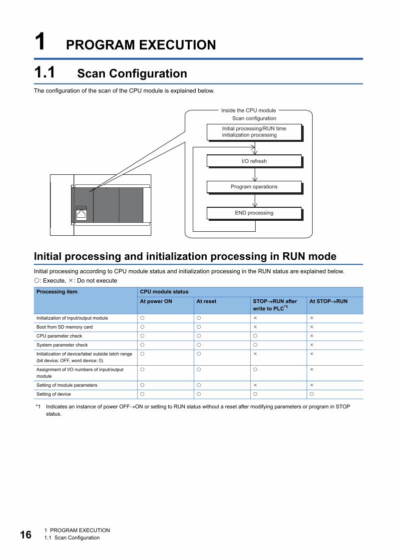
The configuration of the scan of the CPU module is explained below.
Initial processing and initialization processing in RUN mode
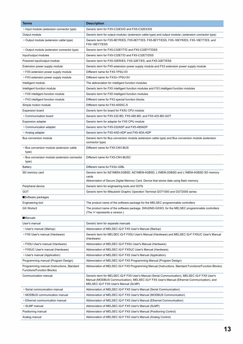
Initial processing according to CPU module status and initialization processing in the RUN status are explained below.
: Execute, : Do not execute
*1 Indicates an instance of power OFFON or setting to RUN status without a reset after modifying parameters or program in STOP
status.
Processing item CPU module status
At power ON At reset STOPRUN after
write to PLC*1At STOPRUN
Initialization of input/output module
Boot from SD memory card
CPU parameter check
System parameter check
Initialization of device/label outside latch range
(bit device: OFF, word device: 0)
Assignment of I/O numbers of input/output
module
Setting of module parameters
Setting of device
Inside the CPU module
Scan configuration
Program operations
END processing
Initial processing/RUN time
initialization processing
I/O refresh
1 PROGRAM EXECUTION
1.1 Scan Configuration 17
1
I/O refresh
Execute I/O refresh before starting program operations.
� Input ON/OFF data input from input module/intelligent function module to CPU module
� Output ON/OFF data input from CPU module to output module/intelligent function module
When executing constant scan, I/O refresh is executed after the constant scan waiting time ends.
Program operations
Step 0 of each program up to the END/FEND instruction is executed according to program settings. This program is called the
"main routine." Main routine programs can be divided into subroutines. (Page 29 Subroutine program)
END processing
END processing involves the following processes:
� Refreshing of network modules
� Refreshing of intelligent function modules
� Instruction termination processing
� Device/label access service processing
� Resetting of the watchdog timer
� Self-diagnostic processing
� Setting of values to special relays/special registers (set timing: when END processing is executed)
181 PROGRAM EXECUTION
1.2 Scan Time
1.2 Scan Time
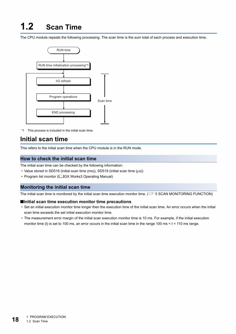
The CPU module repeats the following processing. The scan time is the sum total of each process and execution time.
*1 This process is included in the initial scan time.
Initial scan time
This refers to the initial scan time when the CPU module is in the RUN mode.
How to check the initial scan time
The initial scan time can be checked by the following information:
� Value stored in SD518 (initial scan time (ms)), SD519 (initial scan time (s))
� Program list monitor (GX Works3 Operating Manual)
Monitoring the initial scan time
The initial scan time is monitored by the initial scan time execution monitor time. (5 SCAN MONITORING FUNCTION)
■Initial scan time execution monitor time precautions � Set an initial execution monitor time longer then the execution time of the initial scan time. An error occurs when the initial
scan time exceeds the set initial execution monitor time.
� The measurement error margin of the initial scan execution monitor time is 10 ms. For example, if the initial execution
monitor time (t) is set to 100 ms, an error occurs in the initial scan time in the range 100 ms < t < 110 ms range.
I/O refresh
Program operations
END processing
RUN time
Scan time
RUN time initialization processing*1
1 PROGRAM EXECUTION
1.3 Program Execution Sequence 19
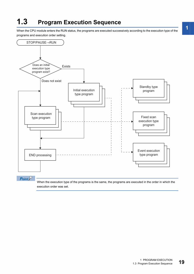
11.3 Program Execution Sequence
When the CPU module enters the RUN status, the programs are executed successively according to the execution type of the
programs and execution order setting.
When the execution type of the programs is the same, the programs are executed in the order in which the
execution order was set.
STOP/PAUSE→RUN
END processing
Initial execution
type program
Scan execution
type program
Event execution
type program
Fixed scan
execution type
program
Standby type
program
Exists
Does not exist
Does an initial
execution type
program exist?
201 PROGRAM EXECUTION
1.4 Execution Type of Program
1.4 Execution Type of Program
Set the program execution conditions.
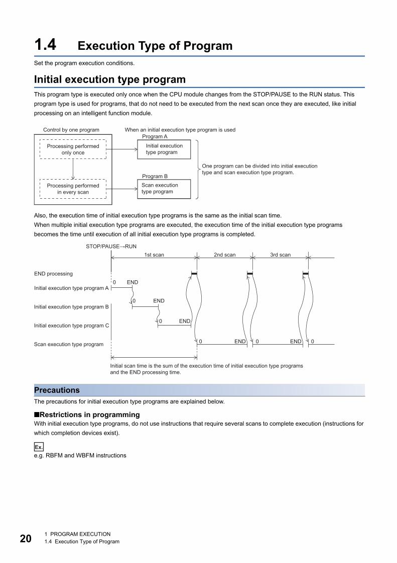
Initial execution type program
This program type is executed only once when the CPU module changes from the STOP/PAUSE to the RUN status. This
program type is used for programs, that do not need to be executed from the next scan once they are executed, like initial
processing on an intelligent function module.
Also, the execution time of initial execution type programs is the same as the initial scan time.
When multiple initial execution type programs are executed, the execution time of the initial execution type programs
becomes the time until execution of all initial execution type programs is completed.
Precautions
The precautions for initial execution type programs are explained below.
■Restrictions in programmingWith initial execution type programs, do not use instructions that require several scans to complete execution (instructions for
which completion devices exist).
Ex.
e.g. RBFM and WBFM instructions
When an initial execution type program is used
Program A
Program B
Control by one program
Initial execution
type program
Scan execution
type program
One program can be divided into initial execution
type and scan execution type program.
Processing performed
only once
Processing performed
in every scan
1st scan 2nd scan 3rd scan
STOP/PAUSE→RUN
END processing
Initial execution type program A
Initial execution type program B
Scan execution type program
Initial execution type program C
0 END
0 END
0
0
END
0END 0END
Initial scan time is the sum of the execution time of initial execution type programs
and the END processing time.
1 PROGRAM EXECUTION
1.4 Execution Type of Program 21
1
Scan execution type program
This program type is executed only once per scan from the scan following the scan where an initial execution type program
was executed.
When multiple scan execution type programs are executed, the execution time of the scan execution type programs becomes
the time until execution of all scan execution type programs is completed. Note, however, that when an program/event
execution type program is executed before a scan execution type program is completed, the execution time of these
programs is included in the scan time.
Fixed scan execution type program
An interrupt program which is executed at a specified time interval. Different from the normal interrupt program, this type of
program does not require interrupt pointer (I) and IRET instruction to be written (pointer is assigned by parameter). Execution
is performed by program file basis.
You can use 4 files of fixed scan execution type programs at the maximum.
To execute a fixed scan execution type program, the EI instruction must be used to enable interrupts.
1st scan 2nd scan 3rd scan 4th scan
STOP/PAUSE→RUN
END processing
Initial execution type program
Scan execution type program A
Scan execution type program C
Scan execution type program B
Scan time
0 END
0 END
0 END
0 END
0 END
END
0 END
0
Fixed scan interval
END processing
Scan execution type program
Fixed scan execution type program
Condition
established
Condition
established
221 PROGRAM EXECUTION
1.4 Execution Type of Program
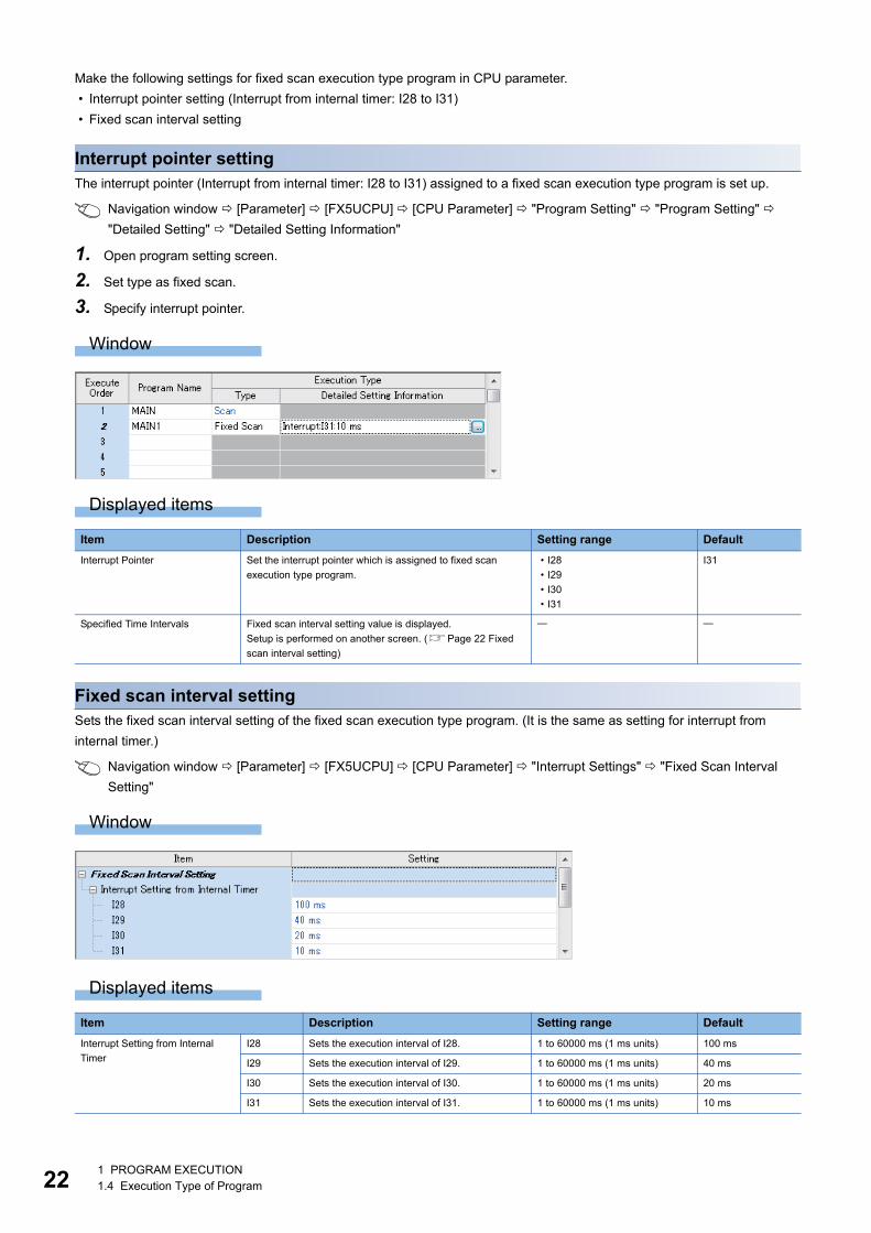
Make the following settings for fixed scan execution type program in CPU parameter.
� Interrupt pointer setting (Interrupt from internal timer: I28 to I31)
� Fixed scan interval setting
Interrupt pointer setting
The interrupt pointer (Interrupt from internal timer: I28 to I31) assigned to a fixed scan execution type program is set up.
Navigation window [Parameter] [FX5UCPU] [CPU Parameter] "Program Setting" "Program Setting"
"Detailed Setting" "Detailed Setting Information"
1. Open program setting screen.
2. Set type as fixed scan.
3. Specify interrupt pointer.
Window
Displayed items
Fixed scan interval setting
Sets the fixed scan interval setting of the fixed scan execution type program. (It is the same as setting for interrupt from
internal timer.)
Navigation window [Parameter] [FX5UCPU] [CPU Parameter] "Interrupt Settings" "Fixed Scan Interval
Setting"
Window
Displayed items
Item Description Setting range Default
Interrupt Pointer Set the interrupt pointer which is assigned to fixed scan
execution type program.
� I28
� I29
� I30
� I31
I31
Specified Time Intervals Fixed scan interval setting value is displayed.
Setup is performed on another screen. (Page 22 Fixed
scan interval setting)
Item Description Setting range Default
Interrupt Setting from Internal
Timer
I28 Sets the execution interval of I28. 1 to 60000 ms (1 ms units) 100 ms
I29 Sets the execution interval of I29. 1 to 60000 ms (1 ms units) 40 ms
I30 Sets the execution interval of I30. 1 to 60000 ms (1 ms units) 20 ms
I31 Sets the execution interval of I31. 1 to 60000 ms (1 ms units) 10 ms
1 PROGRAM EXECUTION
1.4 Execution Type of Program 23
1
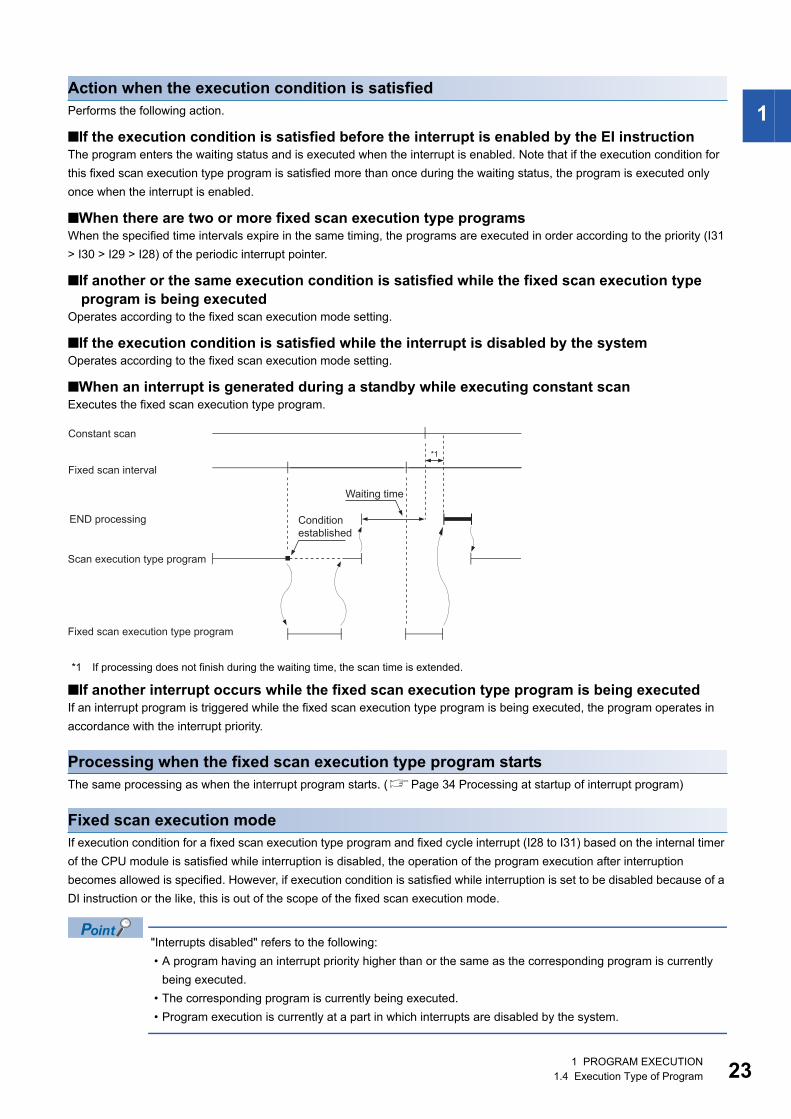
Action when the execution condition is satisfied
Performs the following action.
■If the execution condition is satisfied before the interrupt is enabled by the EI instructionThe program enters the waiting status and is executed when the interrupt is enabled. Note that if the execution condition for
this fixed scan execution type program is satisfied more than once during the waiting status, the program is executed only
once when the interrupt is enabled.
■When there are two or more fixed scan execution type programsWhen the specified time intervals expire in the same timing, the programs are executed in order according to the priority (I31
> I30 > I29 > I28) of the periodic interrupt pointer.
■If another or the same execution condition is satisfied while the fixed scan execution type
program is being executedOperates according to the fixed scan execution mode setting.
■If the execution condition is satisfied while the interrupt is disabled by the systemOperates according to the fixed scan execution mode setting.
■When an interrupt is generated during a standby while executing constant scanExecutes the fixed scan execution type program.
*1 If processing does not finish during the waiting time, the scan time is extended.
■If another interrupt occurs while the fixed scan execution type program is being executedIf an interrupt program is triggered while the fixed scan execution type program is being executed, the program operates in
accordance with the interrupt priority.
Processing when the fixed scan execution type program starts
The same processing as when the interrupt program starts. (Page 34 Processing at startup of interrupt program)
Fixed scan execution mode
If execution condition for a fixed scan execution type program and fixed cycle interrupt (I28 to I31) based on the internal timer
of the CPU module is satisfied while interruption is disabled, the operation of the program execution after interruption
becomes allowed is specified. However, if execution condition is satisfied while interruption is set to be disabled because of a
DI instruction or the like, this is out of the scope of the fixed scan execution mode.
"Interrupts disabled" refers to the following:
� A program having an interrupt priority higher than or the same as the corresponding program is currently
being executed.
� The corresponding program is currently being executed.
� Program execution is currently at a part in which interrupts are disabled by the system.
Fixed scan interval
END processing
Scan execution type program
Fixed scan execution type program
Condition
established
Constant scan
*1
Waiting time
241 PROGRAM EXECUTION
1.4 Execution Type of Program
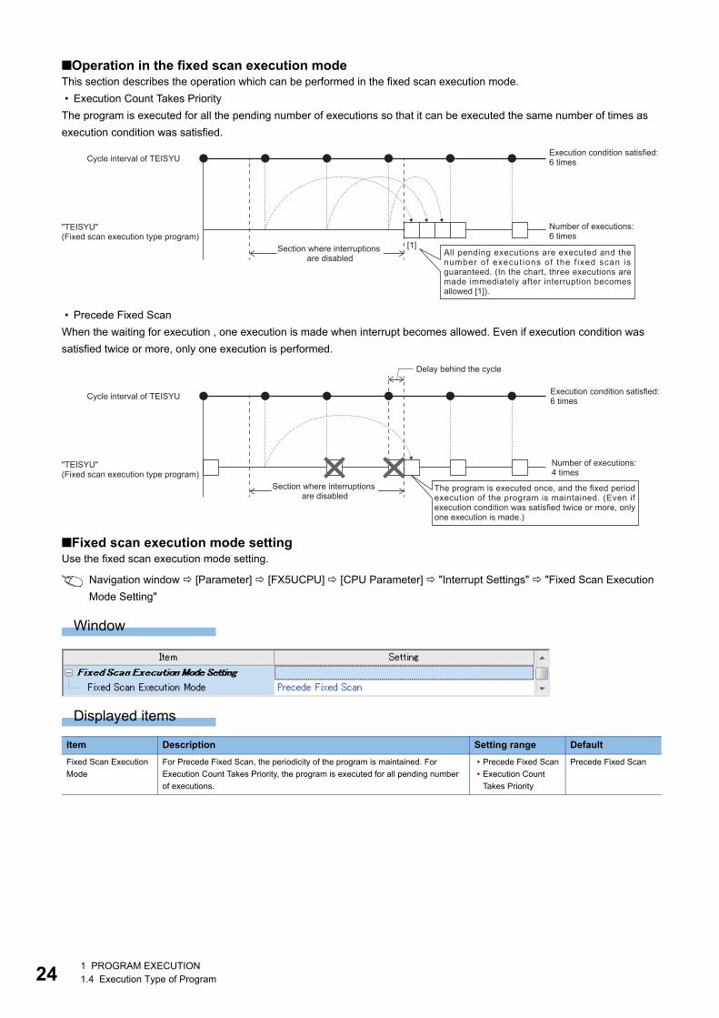
■Operation in the fixed scan execution modeThis section describes the operation which can be performed in the fixed scan execution mode.
� Execution Count Takes Priority
The program is executed for all the pending number of executions so that it can be executed the same number of times as
execution condition was satisfied.
� Precede Fixed Scan
When the waiting for execution , one execution is made when interrupt becomes allowed. Even if execution condition was
satisfied twice or more, only one execution is performed.
■Fixed scan execution mode settingUse the fixed scan execution mode setting.
Navigation window [Parameter] [FX5UCPU] [CPU Parameter] "Interrupt Settings" "Fixed Scan Execution
Mode Setting"
Window
Displayed items
Item Description Setting range Default
Fixed Scan Execution
Mode
For Precede Fixed Scan, the periodicity of the program is maintained. For
Execution Count Takes Priority, the program is executed for all pending number
of executions.
� Precede Fixed Scan
� Execution Count
Takes Priority
Precede Fixed Scan
[1]
Execution condition satisfied: 6 timesCycle interval of TEISYU
"TEISYU"(Fixed scan execution type program)
Number of executions: 6 times
All pending executions are executed and the number of execut ions of the f ixed scan is guaranteed. (In the chart, three executions are made immediately after interruption becomes allowed [1]).
Section where interruptions are disabled
Section where interruptions are disabled
Execution condition satisfied: 6 times
Delay behind the cycle
Cycle interval of TEISYU
"TEISYU"(Fixed scan execution type program)
Number of executions: 4 times
The program is executed once, and the fixed period execution of the program is maintained. (Even if execution condition was satisfied twice or more, only one execution is made.)
1 PROGRAM EXECUTION
1.4 Execution Type of Program 25
1
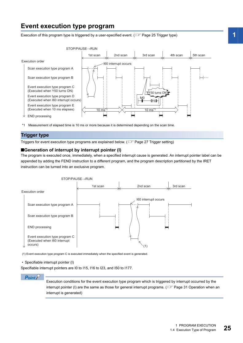
Event execution type program
Execution of this program type is triggered by a user-specified event. (Page 25 Trigger type)
*1 Measurement of elapsed time is 10 ms or more because it is determined depending on the scan time.
Trigger type
Triggers for event execution type programs are explained below. (Page 27 Trigger setting)
■Generation of interrupt by interrupt pointer (I)The program is executed once, immediately, when a specified interrupt cause is generated. An interrupt pointer label can be
appended by adding the FEND instruction to a different program, and the program description partitioned by the IRET
instruction can be turned into an exclusive program.
� Specifiable interrupt pointer (I)
Specifiable interrupt pointers are I0 to I15, I16 to I23, and I50 to I177.
Execution conditions for the event execution type program which is triggered by interrupt occurred by the
interrupt pointer (I) are the same as those for general interrupt programs. (Page 31 Operation when an
interrupt is generated)
(1) Event execution type program C is executed immediately when the specified event is generated.
Y50M0
10 ms*1 10 ms*1
1st scan
I60 interrupt occurs
2nd scan 3rd scan 4th scan 5th scan
STOP/PAUSE→RUN
Scan execution type program A
END processing
Scan execution type program B
Execution order
Y50 turns ON
Event execution type program E
(Executed when 10 ms elapses)
Event execution type program D
(Executed when I60 interrupt occurs)
Event execution type program C
(Executed when Y50 turns ON)
(1)
1st scan
I60 interrupt occurs
2nd scan 3rd scan
STOP/PAUSE→RUN
Scan execution type program A
END processing
Scan execution type program B
Execution order
Event execution type program C
(Executed when I60 interrupt
occurs)
261 PROGRAM EXECUTION
1.4 Execution Type of Program
■Bit data ON (TRUE)When it is the turn of the corresponding program to be executed, the program is executed if the specified bit data is ON. This
eliminates the need for creating a program for monitoring triggers in a separate program.
Applicable devices are as follows.
*1 Indexed devices cannot be specified.
■Elapsed timeThe program is executed once when it is the turn of the corresponding program to be executed first after the CPU module is
run and the specified time has elapsed. For second execution onwards, the time is re-calculated from the start of the previous
event execution type program. When it is the turn of the corresponding program to be executed first after specified time has
elapsed, program execution is repeated. Output (Y) currently used in the corresponding program and the current values of
timer (T) can be cleared at the next scan following execution of the corresponding program. This will not be always executing
an interrupt at a constant cycle but can be used when executing a specified program after a specified time has elapsed.
Output and timer current values are not cleared even when the program is set so that output and timer current
values are cleared, if the scan time is longer than the elapsed time set value.
(1) The program is executed if Y50 is ON when it is the turn of event execution type program C to be executed.
Item Description
Device*1 Bit device X (DX), Y, M, L, F, SM, B, SB
Bit specification in word device D, SD, W, SW, R, U\G
(1) When it is the turn of the first execution after the specified time has elapsed, event execution type program C is executed.
Y50M0
Y50M0
(1)
1st scan 2nd scan 3rd scan 4th scan
STOP/PAUSE→RUN
Scan execution type program A
END processing
Scan execution type program B
Execution order
Y50 is the ON interval
Y50 turns OFFY50 turns ON
Event execution type program C
(Executed when Y50 turns ON)
10 ms 10 ms
(1)
1st scan 2nd scan 3rd scan 4th scan
STOP/PAUSE→RUN
Scan execution type program A
END processing
Scan execution type program B
Execution order
Measurement interval
Event execution type program C
(Executed when 10 ms elapses)
Specified time 10
ms has passed
Specified time 10
ms has passed
1 PROGRAM EXECUTION
1.4 Execution Type of Program 27
1
Trigger setting
Use the event execution type detail setting.
Navigation window [Parameter] [FX5UCPU] [CPU Parameter] "Program Setting"
Operating procedure
Displayed items
When "Clear Output and Current Value of Timer" is enabled together with "ON of Bit Data (TRUE)" or
"Passing Time", the current values of the output (Y) and timer (T) of this program can be cleared at the first
execution turn of this program that comes after the trigger turns OFF.
"Program Setting" window 1. Click "Detailed Setting" on the Program Setting.
"Detailed Setting" window 2. Select the program name and set the execution type to
"Event".
3. Click "Detailed Setting Information".
"Event Execution Type Detailed Setting" window 4. Set the trigger type to execute the event execution type
program.
Item Description Setting range Default
Interruption Occurrence Sets the interrupt pointer used as the trigger. I0 to I23, I50 to I177
ON of Bit Data (TRUE) Sets the device used as the trigger. Page 26 Bit data ON (TRUE)
Passing Time Sets the elapsed time. � When "ms" is selected: 1 to
65535 ms (in 1 ms units)
� When "s" is selected: 1 to
65535 s (in 1 s units)
281 PROGRAM EXECUTION
1.4 Execution Type of Program
Stand-by type program
This program is executed only when there is an execution request.
Saving programs in library
Subroutine programs or interrupt programs are saved as standby type programs so that they can be used when controlled
separately from the main routine program. Multiple subroutine programs and interrupt programs can be created in one
standby type program.
How to execute
Execute standby type programs as follows.
� Create sub-routine programs and interrupt programs in the standby type program which is called up by a pointer, etc. or
when an interrupt is generated.
P100
I0
P100
I0
Scan execution type program Scan execution type program
Stand-by type program
Main routine
program
Subroutine
program
Interrupt
program
Main routine
program
Subroutine
program
Interrupt
program
1 PROGRAM EXECUTION
1.5 Program Type 29
11.5 Program Type
Programs that use pointers (P) or interrupt pointers (I) are explained below.
Subroutine program
This is the program from pointer (P) up to the RET instruction. Subroutine programs are executed only when they are called
by the CALL instruction. Pointer type labels also can be used instead of pointers (P). The applications of subroutine programs
are as follows:
� By grouping programs that are executed multiple times in one scan into a single subroutine program, the number of steps
in the entire program can be reduced.
� A program that is executed only under certain conditions can be saved as a subroutine program which shortens the scan
time proportionately.
� Subroutine programs can also be managed as separate programs by turning them into standby type
programs. (Page 28 Stand-by type program)
� Pointers need not be programmed starting with the smallest number.
Precautions
The precautions when using subroutine programs are explained below.
� Do not use timers (T, ST). Note, however, that timers can be used when a timer coil (OUT T instruction) is always
executed only once in one scan.
� An error occurs when program execution returns to the call source program and the program is terminated without using
the RET instruction.
� An error occurs when there is no pointer (P) or pointer type global label in FB or FUN.
RET
END
P1
RET
Y12
RET
Y11
P8
P0
FEND
Y10
Subroutine program 1
Subroutine program 2
Subroutine program 3
Pointer
Main routine program
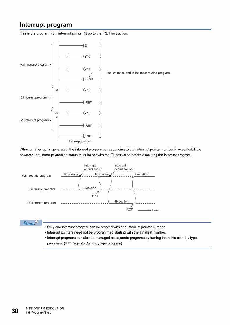
301 PROGRAM EXECUTION
1.5 Program Type
Interrupt program
This is the program from interrupt pointer (I) up to the IRET instruction.
When an interrupt is generated, the interrupt program corresponding to that interrupt pointer number is executed. Note,
however, that interrupt enabled status must be set with the EI instruction before executing the interrupt program.
� Only one interrupt program can be created with one interrupt pointer number.
� Interrupt pointers need not be programmed starting with the smallest number.
� Interrupt programs can also be managed as separate programs by turning them into standby type
programs. (Page 28 Stand-by type program)
I0
I29
Main routine program
I0 interrupt program
I29 interrupt program
Indicates the end of the main routine program.
Interrupt pointer
IRET
IRET
END
FEND
El
Y13
Y12
Y11
Y10
Main routine program
I0 interrupt program
I29 interrupt program
Execution Execution
Execution
Execution
Execution
IRET
IRET
Interrupt
occurs for I0
Interrupt
occurs for I29
Time
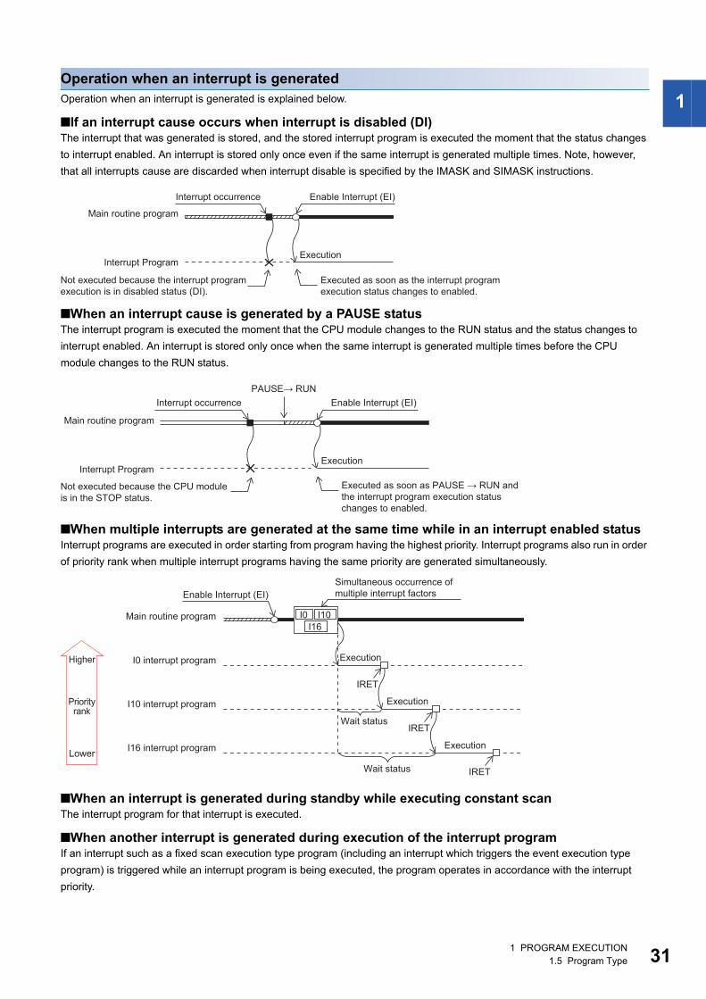
1 PROGRAM EXECUTION
1.5 Program Type 31
1
Operation when an interrupt is generated
Operation when an interrupt is generated is explained below.
■If an interrupt cause occurs when interrupt is disabled (DI)The interrupt that was generated is stored, and the stored interrupt program is executed the moment that the status changes
to interrupt enabled. An interrupt is stored only once even if the same interrupt is generated multiple times. Note, however,
that all interrupts cause are discarded when interrupt disable is specified by the IMASK and SIMASK instructions.
■When an interrupt cause is generated by a PAUSE statusThe interrupt program is executed the moment that the CPU module changes to the RUN status and the status changes to
interrupt enabled. An interrupt is stored only once when the same interrupt is generated multiple times before the CPU
module changes to the RUN status.
■When multiple interrupts are generated at the same time while in an interrupt enabled statusInterrupt programs are executed in order starting from program having the highest priority. Interrupt programs also run in order
of priority rank when multiple interrupt programs having the same priority are generated simultaneously.
■When an interrupt is generated during standby while executing constant scanThe interrupt program for that interrupt is executed.
■When another interrupt is generated during execution of the interrupt programIf an interrupt such as a fixed scan execution type program (including an interrupt which triggers the event execution type
program) is triggered while an interrupt program is being executed, the program operates in accordance with the interrupt
priority.
Main routine program
Not executed because the interrupt program
execution is in disabled status (DI).
Executed as soon as the interrupt program
execution status changes to enabled.
Interrupt Program
Interrupt occurrence Enable Interrupt (EI)
Execution
Executed as soon as PAUSE → RUN and
the interrupt program execution status
changes to enabled.
Not executed because the CPU module
is in the STOP status.
Interrupt occurrence Enable Interrupt (EI)
Execution
Main routine program
Interrupt Program
PAUSE→ RUN
Main routine program
I0 interrupt program
Enable Interrupt (EI)
Simultaneous occurrence of
multiple interrupt factors
Execution
I10 interrupt program Execution
Wait status
Wait status
I16 interrupt program
Priority rank
IRET
IRET
IRET
I0 I10
I16
Execution
Higher
Lower
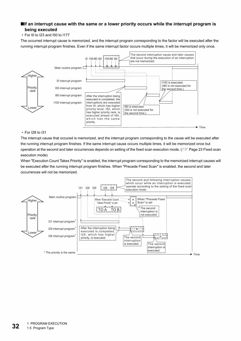
321 PROGRAM EXECUTION
1.5 Program Type
■If an interrupt cause with the same or a lower priority occurs while the interrupt program is
being executed � For I0 to I23 and I50 to I177
The occurred interrupt cause is memorized, and the interrupt program corresponding to the factor will be executed after the
running interrupt program finishes. Even if the same interrupt factor occurs multiple times, it will be memorized only once.
� For I28 to I31
The interrupt cause that occured is memorized, and the interrupt program corresponding to the cause will be executed after
the running interrupt program finishes. If the same interrupt cause occurs multiple times, it will be memorized once but
operation at the second and later occurrences depends on setting of the fixed scan execution mode. (Page 23 Fixed scan
execution mode)
When "Execution Count Takes Priority" is enabled, the interrupt program corresponding to the memorized interrupt causes will
be executed after the running interrupt program finishes. When "Precede Fixed Scan" is enabled, the second and later
occurrences will not be memorized.
I0
Time
Main routine program
I0 interrupt program
I50 interrupt program
I80 interrupt program
I100 interrupt program
I100 I80 I50 I100 I80 I50
The second interruption cause and later causes that occur during the execution of an interruption are not memorized.
After the interruption being executed is completed, the interruptions are executed from I0, which has higher priority level. I50, which has higher priority rank, is executed ahead of I80, w h i c h h a s t h e s a m e priority.
I80 is executed.(I50 is not executed for the second time.)
I100 is executed.(I80 is not executed for the second time.)
Higher
Lower
Priority rank
I31
Time
Main routine program
Higher
Lower
I31 interrupt program*
* The priority is the same.
I29 interrupt program*
I28 interrupt program*
I28 I29 I28
When "Execution Count
Takes Priority" is set
When "Precede Fixed Scan" is set
B
A
I29
TO A TO B
The second and following interruption causes, which occur while an interruption is executed, operate according to the setting of the fixed scan execution mode.
After the interruption being executed is completed, I29 , wh ich has h igher priority, is executed.
The second interruption is not executed.
The second interruption is executed. The second
interruption is executed.
Priority rank
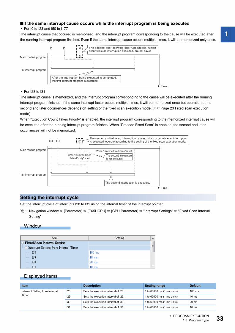
1 PROGRAM EXECUTION
1.5 Program Type 33
1
■If the same interrupt cause occurs while the interrupt program is being executed � For I0 to I23 and I50 to I177
The interrupt cause that occured is memorized, and the interrupt program corresponding to the cause will be executed after
the running interrupt program finishes. Even if the same interrupt cause occurs multiple times, it will be memorized only once.
� For I28 to I31
The interrupt cause is memorized, and the interrupt program corresponding to the cause will be executed after the running
interrupt program finishes. If the same interrupt factor occurs multiple times, it will be memorized once but operation at the
second and later occurrences depends on setting of the fixed scan execution mode. (Page 23 Fixed scan execution
mode)
When "Execution Count Takes Priority" is enabled, the interrupt program corresponding to the memorized interrupt cause will
be executed after the running interrupt program finishes. When "Precede Fixed Scan" is enabled, the second and later
occurrences will not be memorized.
Setting the interrupt cycle
Set the interrupt cycle of interrupts I28 to I31 using the internal timer of the interrupt pointer.
Navigation window [Parameter] [FX5UCPU] [CPU Parameter] "Interrupt Settings" "Fixed Scan Interval
Setting"
Window
Displayed items
Item Description Setting range Default
Interrupt Setting from Internal
Timer
I28 Sets the execution interval of I28. 1 to 60000 ms (1 ms units) 100 ms
I29 Sets the execution interval of I29. 1 to 60000 ms (1 ms units) 40 ms
I30 Sets the execution interval of I30. 1 to 60000 ms (1 ms units) 20 ms
I31 Sets the execution interval of I31. 1 to 60000 ms (1 ms units) 10 ms
I0
Time
Main routine program
I0 interrupt program
I0 I0 The second and following interrupt causes, which occur while an interruption executed, are not saved.
After the interruption being executed is completed, the first interrupt program is executed.
I31
Time
Main routine program
I31 interrupt program
I31 I31
When "Execution Count
Takes Priority" is set
When "Precede Fixed Scan" is set
The second and following interruption causes, which occur while an interruption is executed, operate according to the setting of the fixed scan execution mode.
The second interruption is not executed.
The second interruption is executed.
341 PROGRAM EXECUTION
1.5 Program Type
Processing at startup of interrupt program
Processing is as follows when an interrupt program is started up.
� Purge/restore of index registers (Z, LZ)
■Purge/restore of index registers (Z, LZ)When an interrupt program is started up, the values of the index registers (Z, LZ) in the currently executing program are
purged, and those values are handed over to the interrupt program. Then, when an interrupt program is terminated, the
purged values are restored to the currently executing program.
Precautions
The precautions for interrupt programs are explained below.
■Restrictions in programming � The PLS/PLF instructions execute OFF processing at the scan following instruction execution. ON devices remain ON until
the interrupt program runs again and the instruction is executed.
� Only a routine timer can be used in an interrupt program. Timers (T, ST) cannot be used.
■Splitting of dataProcessing may be interrupted during instruction execution and an interrupt programs can be executed. Accordingly, splitting
of data might occur if the same devices are used by both the interrupt program and the program that is aborted by the
interrupt. Implement the following preventive measure.
� Set instructions that will result in inconsistencies if interrupted to "interrupt disabled" using the DI instruction.
� When using bit data, ensure that the same bit data is not used by both the interrupt program and the program that is
aborted by the interrupt.
■Interrupt precision is not improvedIf interrupt precision is not improved, this might be remedied by implementing the following:
� Give higher priority to the interrupt that needs higher precision.
� Use an interrupt pointer with high interrupt priority order.
� Recheck the section of interruption disabled.
2 PROCESSING OF OPERATIONS ACCORDING TO CPU MODULE OPERATION STATUS
35
2
2 PROCESSING OF OPERATIONS ACCORDING
TO CPU MODULE OPERATION STATUS
The CPU module has three operation statuses as follows:
� RUN status
� STOP status
� Paused
Processing of operations on the CPU module in each status is explained below.
Processing of operations in RUN status
In the RUN mode, operations in the sequence program are executed repeatedly in order step 0END (FEND)
instructionstep 0.
■Output when CPU module enters RUN modeOperation results are output after the sequence program is executed for the duration of one scan.
The device memory other than the output (Y) holds the state immediately before the RUN state. However, if device initial
value is set up, this initial value is set.
■Processing time until start of operationThe processing time from the CPU module switching from STOPRUN up to start of execution of operations in the sequence
program fluctuates according to the system configuration and parameter settings. (Normally, this time is within one second.)
Processing of operations in STOP status
In the STOP status, execution of operations in the sequence program is stopped by the RUN/STOP/RESET switch or a
remote stop. The CPU module also enters the STOP status when a stop error occurs.
■Output when CPU module enters STOP statusWhen the CPU module enters the STOP status, all output points (Y) turn OFF. For device memory other than outputs (Y),
non-latch devices are cleared and latch devices are held.
However, when SM8033 is on and CPU module switches RUNSTOP, it is possible to hold an output state and the current
value of a device.
Processing of operations in paused status
In a paused status, execution of operations in the sequence program is stopped after one scan execution but with outputs and
device memory states held, by a remote pause.
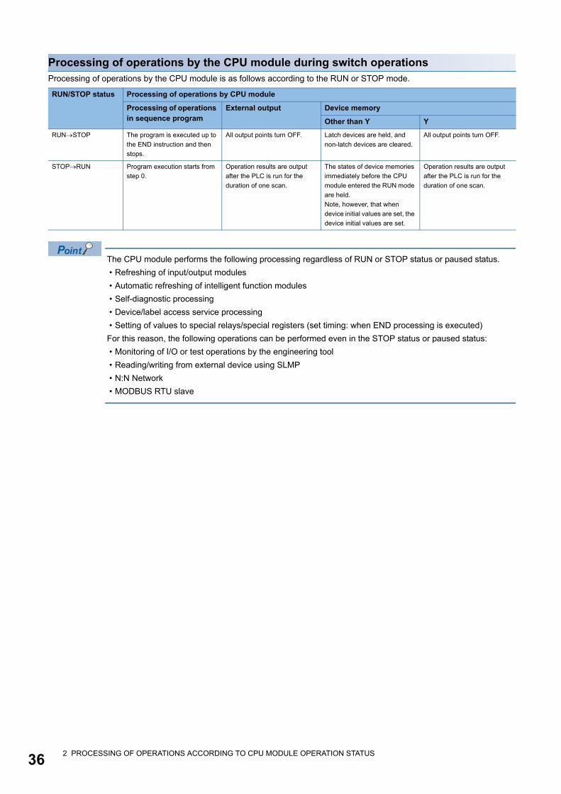
362 PROCESSING OF OPERATIONS ACCORDING TO CPU MODULE OPERATION STATUS
Processing of operations by the CPU module during switch operations
Processing of operations by the CPU module is as follows according to the RUN or STOP mode.
The CPU module performs the following processing regardless of RUN or STOP status or paused status.
� Refreshing of input/output modules
� Automatic refreshing of intelligent function modules
� Self-diagnostic processing
� Device/label access service processing
� Setting of values to special relays/special registers (set timing: when END processing is executed)
For this reason, the following operations can be performed even in the STOP status or paused status:
� Monitoring of I/O or test operations by the engineering tool
� Reading/writing from external device using SLMP
� N:N Network
� MODBUS RTU slave
RUN/STOP status Processing of operations by CPU module
Processing of operations
in sequence program
External output Device memory
Other than Y Y
RUNSTOP The program is executed up to
the END instruction and then
stops.
All output points turn OFF. Latch devices are held, and
non-latch devices are cleared.
All output points turn OFF.
STOPRUN Program execution starts from
step 0.
Operation results are output
after the PLC is run for the
duration of one scan.
The states of device memories
immediately before the CPU
module entered the RUN mode
are held.
Note, however, that when
device initial values are set, the
device initial values are set.
Operation results are output
after the PLC is run for the
duration of one scan.
3 CPU MODULE MEMORY CONFIGURATION
3.1 Memory Configuration 37
3
3 CPU MODULE MEMORY CONFIGURATION
3.1 Memory Configuration
CPU module memory is explained below.
Memory configuration
The configuration of CPU module memory is explained below.
Data memory
The following files are stored in data memory.
Device/label memory
Device/label memory has the following areas.
Memory type Application
CPU built-in memory Data memory The following files are stored in this memory:
� Program files, FB files
� Restored information files
� Parameter files
� Files that contain device comments, etc.
Device/label memory Data areas for internal devices/labels, etc. are located in this memory.
SD memory card This is for storing files that contain device comments, etc. and folders and files that are created
by SD memory card functions.
Category File type Max. number of files Storage area size Remarks
Program Program file 32 1 Mbytes
FB files 16 (Up to 15 for user)
Restored information Restored information files 48 1 Mbytes
Parameters Parameter files common to system 1 1 Mbytes
CPU parameter file 1
Module parameter file 1
Remote password 1
Global label setting file 1
Module extension parameter (for protocol setting) 2
Device initial values file 1
Comments Device comment file 1 2 Mbytes
Area Storage area size Application
Device/label memory (standard) 96 Kbytes R, W, SW, labels, and latch labels can be placed in this memory in variable lengths.
R and W can be backed up in the event of a power interruption only when the optional battery
is installed. Also, latch label capacity can be increased when the battery is installed.
Device/label memory (fast) 24 Kbytes Bit devices, T, ST, C, LC, D, Z, LZ, labels, and latch labels can be placed in this memory in
variable lengths.
For saving device/label memory 25 Kbytes This memory is for saving latch devices and devices in fast area that require a latch in the
event of a power interruption.
383 CPU MODULE MEMORY CONFIGURATION
3.1 Memory Configuration
SD memory card
The following files are stored in SD memory card.
Category File type Max. number of files Storage area size Remarks
Program Program file 32 1 Mbytes
FB files 16 (Up to 15 for user)
Restored information Restored information files 48 1 Mbytes
Parameters Parameter files common to system 1 1 Mbytes
CPU parameter file 1
Module parameter file 1
Memory card parameter 1
Remote password 1
Global label setting file 1
Module extension parameter (for protocol setting) 2
Initial device value file 1
Comments Device comment file 1 2 Mbytes
3 CPU MODULE MEMORY CONFIGURATION
3.2 Files 39
3
3.2 Files
The CPU module files are explained below.
File type and storage destination memory
File types and their storage destination memory are explained below.
: Can be stored, : Cannot be stored
*1 For serial communications file.
*2 For Ethernet file.
Executable file operations
File operations that can be executed on each file are explained below. This operation is possible only when the operation
status of the CPU module is the STOP status.
: Can be executed, : No corresponding operation
File type CPU built-in memory SD memory card File name (extension)
Data memory
Drive No.4 Drive No.2
Program Arbitrary.PRG
FB files Arbitrary.PFB
CPU parameters CPU.PRM
System parameters SYSTEM.PRM
Module parameters UNIT.PRM
Memory card parameter MEMCARD.PRM
Device comments Arbitrary.DCM
Device initial values Arbitrary.DID
Global label settings GLBLINF.IFG
Module extension parameter (for protocol setting) UEX3FF01.PPR*1
UEX3FF00.PPR*2
Restored information CallTreeInfo.CAB
SourceInfo.CAB
File type Operation with engineering tool
Write Read Delete
Program
FB files
Parameters
Device comments
Device initial values
Global label setting file
Restored information

403 CPU MODULE MEMORY CONFIGURATION
3.2 Files
MEMO
41
PA
RT
2
PART 2 FUNCTIONS
This part consists of the following chapters.
4 FUNCTION LIST
5 SCAN MONITORING FUNCTION
6 CLOCK FUNCTION
7 ONLINE CHANGE
8 INTERRUPT FUNCTION
9 PID CONTROL FUNCTION
10 CONSTANT SCAN
11 REMOTE OPERATION
12 DEVICE/LABEL MEMORY AREA SETTING
13 INITIAL DEVICE VALUE SETTING
14 LATCH FUNCTION
15 MEMORY CARD FUNCTION
16 DEVICE/LABEL ACCESS SERVICE PROCESSING SETTING
17 RAS FUNCTIONS
18 SECURITY FUNCTIONS
19 BUILT-IN I/O FUNCTION
20 BUILT-IN ANALOG FUNCTION
424 FUNCTION LIST
4 FUNCTION LIST
The following table lists the functions of the CPU module.
Function Description Reference
Scan monitoring function
(Watchdog timer setting)
Detects an error in the hardware and program of the CPU module by
monitoring the scan time.
Page 44
Clock function This function is used for the time management in the function which
the system operates such as the date of the error history.
Page 46
Online change Changing ladder blocks
while online
Writes the part of a program edited on the ladder editor using the
engineering tool to the CPU module in units of ladder blocks. Edited
contents spanning multiple portions can be written to the CPU
module at once.
Page 50
Interrupt function Multiple interrupt function When an interrupt occurs while an interrupt program triggered by
another cause is running, stops the program if its priority is lower
than that of the new interrupt, and runs the higher-priority program
whenever its execution condition is satisfied.
Page 53
PID control function Performs PID control by the PID control instruction. Page 55
Constant scan Keeps the scan time constant and executes program repeatedly. Page 84
Remote operation Remote RUN/STOP Changes the CPU module status to the RUN/STOP/PAUSE status
externally while the RUN/STOP/RESET switch of the CPU module is
in RUN status.
Page 86
Remote PAUSE
Remote RESET Resets the CPU module externally while the CPU module is in the
STOP status.
Device/label memory area setting Sets the capacity of each area in the device/label memory. Page 92
Initial device value setting Sets the initial values of devices used in the program directly (not via
the program) to the devices.
Page 97
Latch function Holds the contents of the device and label of the CPU module when
the power is turned ON etc.
Page 99
Memory card function SD memory card forced
stop
Makes the SD memory card unavailable without turning OFF the
power even when the function accessing the SD memory card is
executed.
Page 103
Boot operation Transfers the file stored in the SD memory card to the transfer
destination memory judged automatically by the CPU module when
the power is turned ON or is reset.
Device/label access service processing setting Sets the number of execution times of the device/label access
service processing executed by END processing, with parameter.
Page 107
RAS function Self-diagnostics function Self-diagnoses the CPU module to see whether an error exist or not. Page 109
Error clear Batch-clears all the continuation errors being detected.
Security function Protects resources stored in PCs and resources in the units in the
system of the FX5 from illegal access by a third party such as theft,
alteration, accidental operation and unauthorized execution.
Page 113
GX Works3 Operating
Manual
Built-in
input/
output
function
High-speed counter function Performs high-speed counter, pulse width measurement, input
interruption, timer interruption, high-speed counter interruption, etc.
by using the input of the CPU module.
Page 114
Pulse width measurement function
Input interrupt function
Timer interrupt function
High-speed counter interrupt function
Built-in positioning function Executes positioning operation of up to 4 axes by using the
transistor output of the CPU module.
MELSEC iQ-F FX5 User's
Manual (Positioning
Control)
PWM output function Executes a PWM output by using the transistor output of the CPU
module.
Page 193
Built-in
analog
function
Analog input function Two analog inputs and one analog output are built in the FX5U CPU
module so that voltage input/voltage output can be performed.
Page 201
MELSEC iQ-F FX5 User's
Manual (Analog Control)Analog output function
Built-in Ethernet function A function related to the Ethernet such as the connection with the
MELSOFT products and GOTs, and socket communication.
MELSEC iQ-F FX5 User's
Manual (Ethernet
Communication)
Serial communication function A function related to the serial communication such as N:N Network,
MC protocol, inverter communication function and non-protocol
communication.
MELSEC iQ-F FX5 User's
Manual (Serial
Communication)

4 FUNCTION LIST
43
4
MODBUS RTU communication function Connection with the products which support MODBUS RTU is
available. The master and slave functions can be used.
MELSEC iQ-F FX5 User's
Manual (MODBUS
Communication)
Function Description Reference
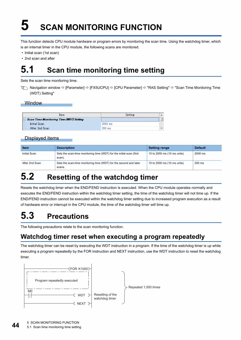
445 SCAN MONITORING FUNCTION
5.1 Scan time monitoring time setting
5 SCAN MONITORING FUNCTION
This function detects CPU module hardware or program errors by monitoring the scan time. Using the watchdog timer, which
is an internal timer in the CPU module, the following scans are monitored.
� Initial scan (1st scan)
� 2nd scan and after
5.1 Scan time monitoring time setting
Sets the scan time monitoring time.
Navigation window [Parameter] [FX5UCPU] [CPU Parameter] "RAS Setting" "Scan Time Monitoring Time
(WDT) Setting"
Window
Displayed items
5.2 Resetting of the watchdog timer
Resets the watchdog timer when the END/FEND instruction is executed. When the CPU module operates normally and
executes the END/FEND instruction within the watchdog timer setting, the time of the watchdog timer will not time up. If the
END/FEND instruction cannot be executed within the watchdog timer setting due to increased program execution as a result
of hardware error or interrupt in the CPU module, the time of the watchdog timer will time up.
5.3 Precautions
The following precautions relate to the scan monitoring function.
Watchdog timer reset when executing a program repeatedly
The watchdog timer can be reset by executing the WDT instruction in a program. If the time of the watchdog timer is up while
executing a program repeatedly by the FOR instruction and NEXT instruction, use the WDT instruction to reset the watchdog
timer.
Item Description Setting range Default
Initial Scan Sets the scan-time monitoring time (WDT) for the initial scan (first
scan).
10 to 2000 ms (10 ms units) 2000 ms
After 2nd Scan Sets the scan-time monitoring time (WDT) for the second and later
scans.
10 to 2000 ms (10 ms units) 200 ms
FOR K1000
WDT
NEXT
Program repeatedly executed
Resetting of the
watchdog timer
Repeated 1,000 times
M0
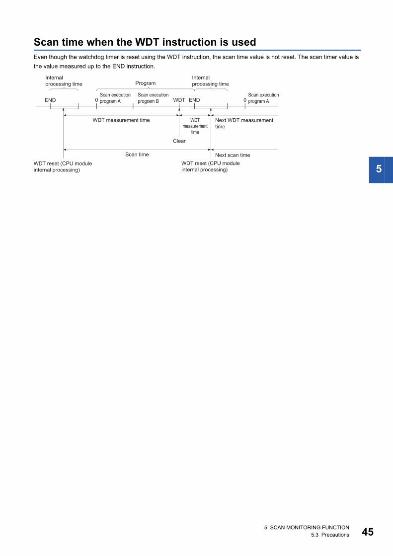
5 SCAN MONITORING FUNCTION
5.3 Precautions 45
5
Scan time when the WDT instruction is used
Even though the watchdog timer is reset using the WDT instruction, the scan time value is not reset. The scan timer value is
the value measured up to the END instruction.
Internal
processing time ProgramInternal
processing time
Scan execution
program A
Scan execution
program B
WDT reset (CPU module
internal processing)
END 0 ENDWDTScan execution
program A0
Scan time
Clear
WDT measurement time WDT measurement
time
Next scan time
Next WDT measurement
time
WDT reset (CPU module
internal processing)
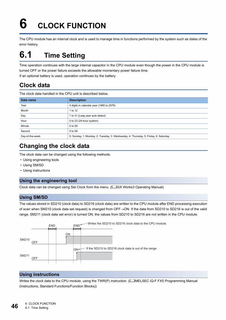
466 CLOCK FUNCTION
6.1 Time Setting
6 CLOCK FUNCTION
The CPU module has an internal clock and is used to manage time in functions performed by the system such as dates of the
error history.
6.1 Time Setting
Time operation continues with the large internal capacitor in the CPU module even though the power in the CPU module is
turned OFF or the power failure exceeds the allowable momentary power failure time.
If an optional battery is used, operation continues by the battery.
Clock data
The clock data handled in the CPU unit is described below.
Changing the clock data
The clock data can be changed using the following methods.
� Using engineering tools
� Using SM/SD
� Using instructions
Using the engineering tool
Clock data can be changed using Set Clock from the menu. (GX Works3 Operating Manual)
Using SM/SD
The values stored in SD210 (clock data) to SD216 (clock data) are written to the CPU module after END processing execution
of scan when SM210 (clock data set request) is changed from OFFON. If the data from SD210 to SD216 is out of the valid
range, SM211 (clock data set error) is turned ON, the values from SD210 to SD216 are not written in the CPU module.
Using instructions
Writes the clock data to the CPU module, using the TWR(P) instruction. (MELSEC iQ-F FX5 Programming Manual
(Instructions, Standard Functions/Function Blocks))
Data name Description
Year 4 digits in calendar year (1980 to 2079)
Month 1 to 12
Day 1 to 31 (Leap year auto detect)
Hour 0 to 23 (24-hour system)
Minute 0 to 59
Second 0 to 59
Day-of-the-week 0: Sunday, 1: Monday, 2: Tuesday, 3: Wednesday, 4: Thursday, 5: Friday, 6: Saturday
ENDEND
ON
Writes the SD210 to SD216 clock data to the CPU module.
If the SD210 to SD216 clock data is out of the rangeON
OFF
OFF
SM211
SM210
6 CLOCK FUNCTION
6.1 Time Setting 47
6
Reading clock data
There are the following methods to read clock data.
� Using SM/SD
� Using instructions
Using SM/SD
Clock data is read to SD210 to SD216 when SM213 (clock data read request) is turned ON.
Using instructions
Clock data is read from the CPU module using the TRD(P) instruction. (MELSEC iQ-F FX5 Programming Manual
(Instructions, Standard Functions/Function Blocks))
Precautions
The following describes precautions when setting the time.
When setting the clock for the first time
The clock is not set when the product is shipped.
Correcting the clock data
Before correcting any part of the clock data, you must write all data into the CPU module again.
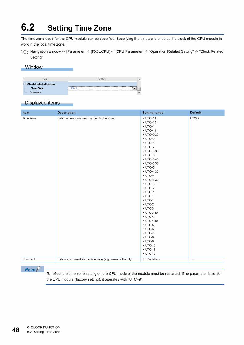
486 CLOCK FUNCTION
6.2 Setting Time Zone
6.2 Setting Time Zone
The time zone used for the CPU module can be specified. Specifying the time zone enables the clock of the CPU module to
work in the local time zone.
Navigation window [Parameter] [FX5UCPU] [CPU Parameter] "Operation Related Setting" "Clock Related
Setting"
Window
Displayed items
To reflect the time zone setting on the CPU module, the module must be restarted. If no parameter is set for
the CPU module (factory setting), it operates with "UTC+9".
Item Description Setting range Default
Time Zone Sets the time zone used by the CPU module. � UTC+13
� UTC+12
� UTC+11
� UTC+10
� UTC+9:30
� UTC+9
� UTC+8
� UTC+7
� UTC+6:30
� UTC+6
� UTC+5:45
� UTC+5:30
� UTC+5
� UTC+4:30
� UTC+4
� UTC+3:30
� UTC+3
� UTC+2
� UTC+1
� UTC
� UTC-1
� UTC-2
� UTC-3
� UTC-3:30
� UTC-4
� UTC-4:30
� UTC-5
� UTC-6
� UTC-7
� UTC-8
� UTC-9
� UTC-10
� UTC-11
� UTC-12
UTC+9
Comment Enters a comment for the time zone (e.g., name of the city). 1 to 32 letters
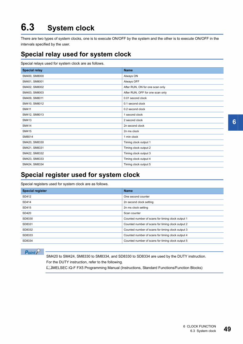
6 CLOCK FUNCTION
6.3 System clock 49
6
6.3 System clock
There are two types of system clocks, one is to execute ON/OFF by the system and the other is to execute ON/OFF in the
intervals specified by the user.
Special relay used for system clock
Special relays used for system clock are as follows.
Special register used for system clock
Special registers used for system clock are as follows.
SM420 to SM424, SM8330 to SM8334, and SD8330 to SD8334 are used by the DUTY instruction.
For the DUTY instruction, refer to the following.
MELSEC iQ-F FX5 Programming Manual (Instructions, Standard Functions/Function Blocks)
Special relay Name
SM400, SM8000 Always ON
SM401, SM8001 Always OFF
SM402, SM8002 After RUN, ON for one scan only
SM403, SM8003 After RUN, OFF for one scan only
SM409, SM8011 0.01 second clock
SM410, SM8012 0.1 second clock
SM411 0.2 second clock
SM412, SM8013 1 second clock
SM413 2 second clock
SM414 2n second clock
SM415 2n ms clock
SM8014 1 min clock
SM420, SM8330 Timing clock output 1
SM421, SM8331 Timing clock output 2
SM422, SM8332 Timing clock output 3
SM423, SM8333 Timing clock output 4
SM424, SM8334 Timing clock output 5
Special register Name
SD412 One second counter
SD414 2n second clock setting
SD415 2n ms clock setting
SD420 Scan counter
SD8330 Counted number of scans for timing clock output 1
SD8331 Counted number of scans for timing clock output 2
SD8332 Counted number of scans for timing clock output 3
SD8333 Counted number of scans for timing clock output 4
SD8334 Counted number of scans for timing clock output 5
507 ONLINE CHANGE
7.1 Online Ladder Block Change
7 ONLINE CHANGE
This chapter describes online change.
7.1 Online Ladder Block Change
Writes the portion edited on the ladder edit window of the engineering tool to the CPU module in increments of ladders. Edited
contents spanning multiple files or multiple portions can be written to the CPU module at once.
For details on the operating procedure of online ladder block change on engineering tools, refer to the
following.
GX Works3 Operating Manual
Editable contents
Within a program block, instructions and pointers (P, I) can be added, changed, or deleted. Also, as POU unit, program blocks
can be added, changed, or deleted. However, when the program/FB file is not in agreement between engineering tool and a
CPU module, it cannot be added, changed, or deleted.
Range changeable in a single session
The following shows the number of steps and number of ladder blocks which can be changed in a single session.
� Number of ladder blocks in a file: 64 blocks or less (2048 steps or less)
� The total of the changed circuit block count in all files: 256 blocks or less
� The total capacity of the program file and the FB file after a change: 1 M byte or less
Online ladder block change during the boot operation
If online change of ladder block is executed from the SD memory card during boot operation, the corresponding file in the SD
memory card, which is the boot source, can be changed as well.
Precautions
This section describes the precautions on using online ladder block change.
Prohibited operation at online ladder block change
When an online change of ladder block, if the power is turned OFF or a reset is made, the process does not end normally.
Such operation is made, execute rewriting to the PLC.
When deleting OUT instruction which is on
When deleting an OUT instruction (coil) which is not necessary for control, be sure to check that the OUT instruction is off
before deleting it. If the OUT instruction is deleted without turning it off in advance, the output will be retained.
Program file not registered in program setting
A program file which is not registered in parameter setting cannot be written.
Initializing the last execution if the ladder at online ladder block change has an FB call
� If a subroutine type FB is called in a FB definition, the execution information of the previous time in the FB definition of the
subroutine type FB is not initialized.
� If a macro type FB is called in the FB definition of a subroutine type, the execution information of the previous time in the
part equivalent to the macro type FB is not initialized either.
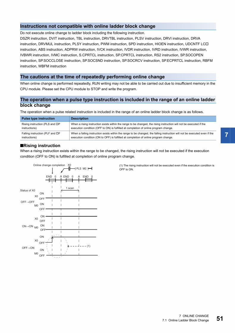
7 ONLINE CHANGE
7.1 Online Ladder Block Change 51
7
Instructions not compatible with online ladder block change
Do not execute online change to ladder block including the following instruction.
DSZR instruction, DVIT instruction, TBL instruction, DRVTBL instruction, PLSV instruction, DRVI instruction, DRVA
instruction, DRVMUL instruction, PLSY instruction, PWM instruction, SPD instruction, HIOEN instruction, UDCNTF LC
instruction, ABS instruction, ADPRW instruction, IVCK instruction, IVDR instruction, IVRD instruction, IVWR instruction,
IVBWR instruction, IVMC instruction, S.CPRTCL instruction, SP.CPRTCL instruction, RS2 instruction, SP.SOCOPEN
instruction, SP.SOCCLOSE instruction, SP.SOCSND instruction, SP.SOCRCV instruction, SP.ECPRTCL instruction, RBFM
instruction, WBFM instruction
The cautions at the time of repeatedly performing online change
When online change is performed repeatedly, RUN writing may not be able to be carried out due to insufficient memory in the
CPU module. Please set the CPU module to STOP and write the program.
The operation when a pulse type instruction is included in the range of an online ladder block change
The operation when a pulse related instruction is included in the range of an online ladder block change is as follows.
■Rising instructionWhen a rising instruction exists within the range to be changed, the rising instruction will not be executed if the execution
condition (OFF to ON) is fulfilled at completion of online program change.
Pulse type instruction Description
Rising instruction (PLS and P
instructions)
When a rising instruction exists within the range to be changed, the rising instruction will not be executed if the
execution condition (OFF to ON) is fulfilled at completion of online program change.
Falling instruction (PLF and F
instructions)
When a falling instruction exists within the range to be changed, the falling instruction will not be executed even if the
execution condition (ON to OFF) is fulfilled at completion of online program change.
(1) The rising instruction will not be executed even if the execution condition is
OFF to ON.
Online change completion
END
1 scan
END END0 0 0
OFF→OFF
ON
OFF
OFF
OFF
OFF
OFF
OFF
ON
ON
ON
ON
ON
ON→ON
Status of X0
X0
M0
X0
M0
X0
M0
(1)
[ PLS M0 ]
X0
A A
OFF→ON
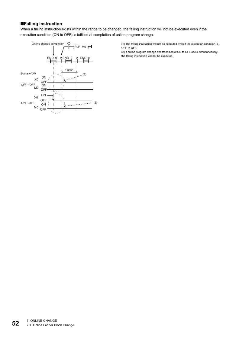
527 ONLINE CHANGE
7.1 Online Ladder Block Change
■Falling instructionWhen a falling instruction exists within the range to be changed, the falling instruction will not be executed even if the
execution condition (ON to OFF) is fulfilled at completion of online program change.
(1) The falling instruction will not be executed even if the execution condition is
OFF to OFF.
(2) If online program change and transition of ON to OFF occur simultaneously,
the falling instruction will not be executed.
Online change completion
END
1 scan
END END0 0 0
OFF→OFF
ON
OFF
OFF
OFF
OFF
ON
ON
ONON→OFF
Status of X0
X0
M0
X0
M0
(1)
[ PLF M0 ]X0
A A
(2)
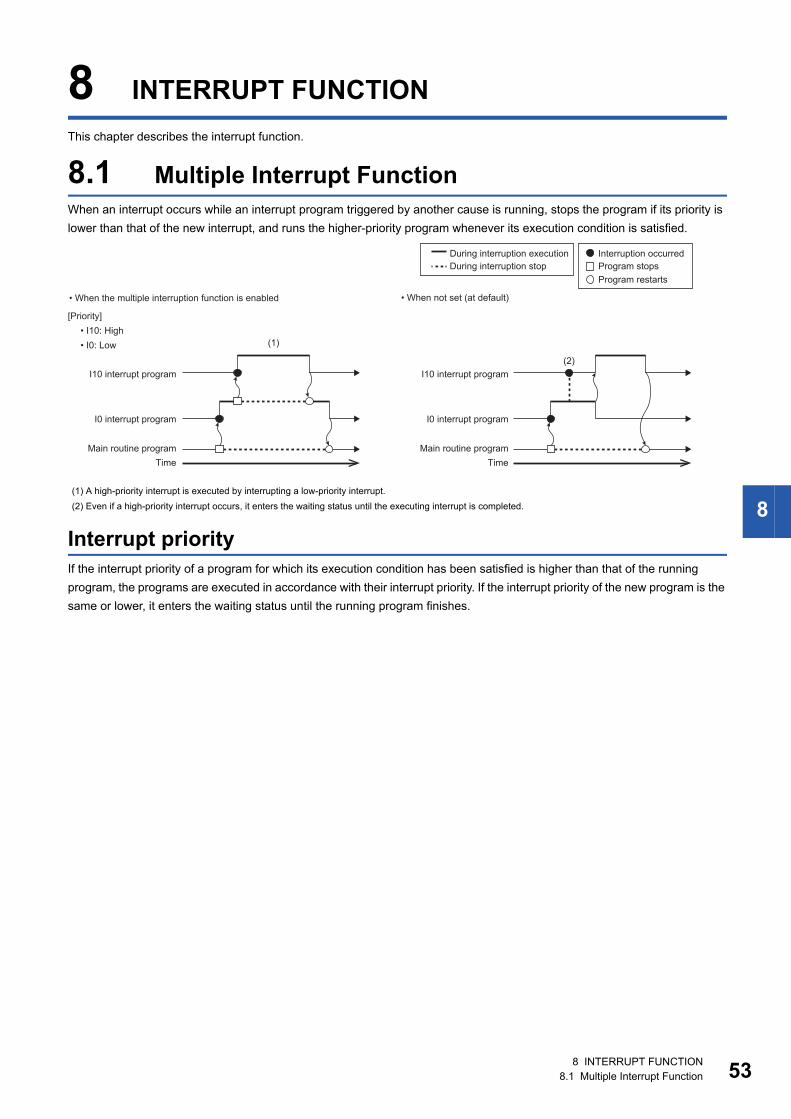
8 INTERRUPT FUNCTION
8.1 Multiple Interrupt Function 53
8
8 INTERRUPT FUNCTION
This chapter describes the interrupt function.
8.1 Multiple Interrupt Function
When an interrupt occurs while an interrupt program triggered by another cause is running, stops the program if its priority is
lower than that of the new interrupt, and runs the higher-priority program whenever its execution condition is satisfied.
Interrupt priority
If the interrupt priority of a program for which its execution condition has been satisfied is higher than that of the running
program, the programs are executed in accordance with their interrupt priority. If the interrupt priority of the new program is the
same or lower, it enters the waiting status until the running program finishes.
(1) A high-priority interrupt is executed by interrupting a low-priority interrupt.
(2) Even if a high-priority interrupt occurs, it enters the waiting status until the executing interrupt is completed.
� When the multiple interruption function is enabled
I10 interrupt program
I0 interrupt program
Main routine program
Time
(1)
� When not set (at default)
During interruption execution
During interruption stop
I10 interrupt program
I0 interrupt program
Main routine program
Time
(2)
[Priority]
� I10: High
� I0: Low
Interruption occurred
Program stops
Program restarts
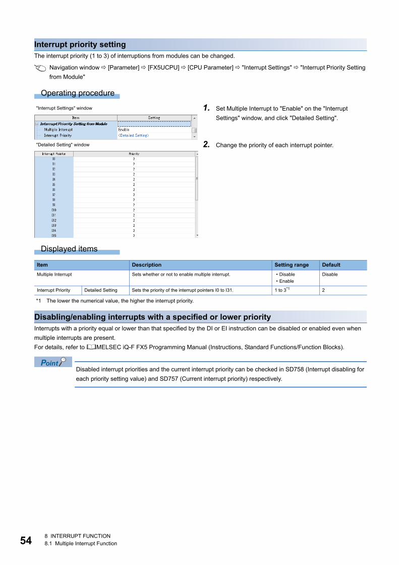
548 INTERRUPT FUNCTION
8.1 Multiple Interrupt Function
Interrupt priority setting
The interrupt priority (1 to 3) of interruptions from modules can be changed.
Navigation window [Parameter] [FX5UCPU] [CPU Parameter] "Interrupt Settings" "Interrupt Priority Setting
from Module"
Operating procedure
Displayed items
*1 The lower the numerical value, the higher the interrupt priority.
Disabling/enabling interrupts with a specified or lower priority
Interrupts with a priority equal or lower than that specified by the DI or EI instruction can be disabled or enabled even when
multiple interrupts are present.
For details, refer to MELSEC iQ-F FX5 Programming Manual (Instructions, Standard Functions/Function Blocks).
Disabled interrupt priorities and the current interrupt priority can be checked in SD758 (Interrupt disabling for
each priority setting value) and SD757 (Current interrupt priority) respectively.
"Interrupt Settings" window 1. Set Multiple Interrupt to "Enable" on the "Interrupt
Settings" window, and click "Detailed Setting".
"Detailed Setting" window 2. Change the priority of each interrupt pointer.
Item Description Setting range Default
Multiple Interrupt Sets whether or not to enable multiple interrupt. � Disable
� Enable
Disable
Interrupt Priority Detailed Setting Sets the priority of the interrupt pointers I0 to I31. 1 to 3*1 2
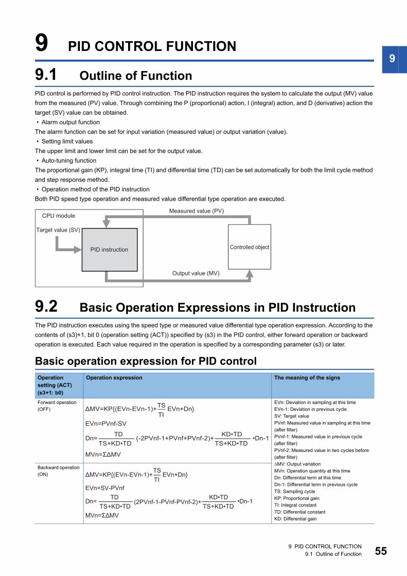
9 PID CONTROL FUNCTION
9.1 Outline of Function 55
99 PID CONTROL FUNCTION
9.1 Outline of Function
PID control is performed by PID control instruction. The PID instruction requires the system to calculate the output (MV) value
from the measured (PV) value. Through combining the P (proportional) action, I (integral) action, and D (derivative) action the
target (SV) value can be obtained.
� Alarm output function
The alarm function can be set for input variation (measured value) or output variation (value).
� Setting limit values
The upper limit and lower limit can be set for the output value.
� Auto-tuning function
The proportional gain (KP), integral time (TI) and differential time (TD) can be set automatically for both the limit cycle method
and step response method.
� Operation method of the PID instruction
Both PID speed type operation and measured value differential type operation are executed.
9.2 Basic Operation Expressions in PID Instruction
The PID instruction executes using the speed type or measured value differential type operation expression. According to the
contents of (s3)+1, bit 0 (operation setting (ACT)) specified by (s3) in the PID control, either forward operation or backward
operation is executed. Each value required in the operation is specified by a corresponding parameter (s3) or later.
Basic operation expression for PID control
Operation
setting (ACT)
(s3+1: b0)
Operation expression The meaning of the signs
Forward operation
(OFF)
EVn: Deviation in sampling at this time
EVn-1: Deviation in previous cycle
SV: Target value
PVnf: Measured value in sampling at this time
(after filter)
PVnf-1: Measured value in previous cycle
(after filter)
PVnf-2: Measured value in two cycles before
(after filter)
MV: Output variation
MVn: Operation quantity at this time
Dn: Differential term at this time
Dn-1: Differential term in previous cycle
TS: Sampling cycle
KP: Proportional gain
TI: Integral constant
TD: Differential constant
KD: Differential gain
Backward operation
(ON)
CPU module
Target value (SV)
Measured value (PV)
Controlled object
Output value (MV)
PID instruction
ΔMV=KP{(EVn-EVn-1)+
EVn=PVnf-SV
Dn=
MVn=ΣΔMV
TS
TI
TD
TS+KD�TD
KD�TD
TS+KD�TD
EVn+Dn}
(-2PVnf-1+PVnf+PVnf-2)+ �Dn-1
ΔMV=KP{(EVn-EVn-1)+
EVn=SV-PVnf
Dn=
MVn=ΣΔMV
TS
TI
TD
TS+KD�TD
KD�TD
TS+KD�TD
EVn+Dn}
(2PVnf-1-PVnf-PVnf-2)+ �Dn-1
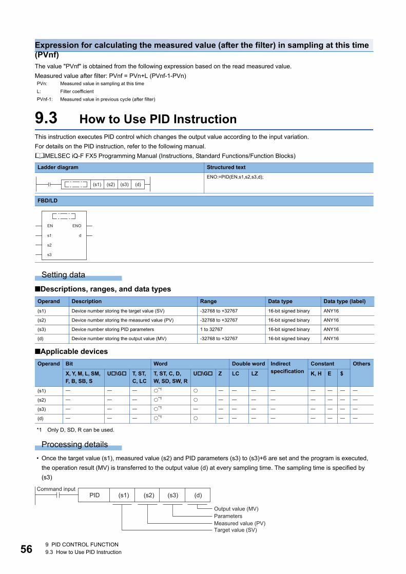
569 PID CONTROL FUNCTION
9.3 How to Use PID Instruction
Expression for calculating the measured value (after the filter) in sampling at this time (PVnf)
The value "PVnf" is obtained from the following expression based on the read measured value.
Measured value after filter: PVnf = PVn+L (PVnf-1-PVn)
9.3 How to Use PID Instruction
This instruction executes PID control which changes the output value according to the input variation.
For details on the PID instruction, refer to the following manual.
MELSEC iQ-F FX5 Programming Manual (Instructions, Standard Functions/Function Blocks)
Setting data
■Descriptions, ranges, and data types
■Applicable devices
*1 Only D, SD, R can be used.
Processing details
� Once the target value (s1), measured value (s2) and PID parameters (s3) to (s3)+6 are set and the program is executed,
the operation result (MV) is transferred to the output value (d) at every sampling time. The sampling time is specified by
(s3)
PVn: Measured value in sampling at this time
L: Filter coefficient
PVnf-1: Measured value in previous cycle (after filter)
Ladder diagram Structured text
ENO:=PID(EN,s1,s2,s3,d);
FBD/LD
Operand Description Range Data type Data type (label)
(s1) Device number storing the target value (SV) -32768 to +32767 16-bit signed binary ANY16
(s2) Device number storing the measured value (PV) -32768 to +32767 16-bit signed binary ANY16
(s3) Device number storing PID parameters 1 to 32767 16-bit signed binary ANY16
(d) Device number storing the output value (MV) -32768 to +32767 16-bit signed binary ANY16
Operand Bit Word Double word Indirect
specification
Constant Others
X, Y, M, L, SM,
F, B, SB, S
U\G T, ST,
C, LC
T, ST, C, D,
W, SD, SW, R
U\G Z LC LZ K, H E $
(s1) *1
(s2) *1
(s3) *1
(d) *1
(s1) (s2) (s3) (d)
EN ENO
ds1
s2
s3
Command input
Target value (SV)
Measured value (PV)
Parameters
Output value (MV)
PID (s1) (s2) (s3) (d)
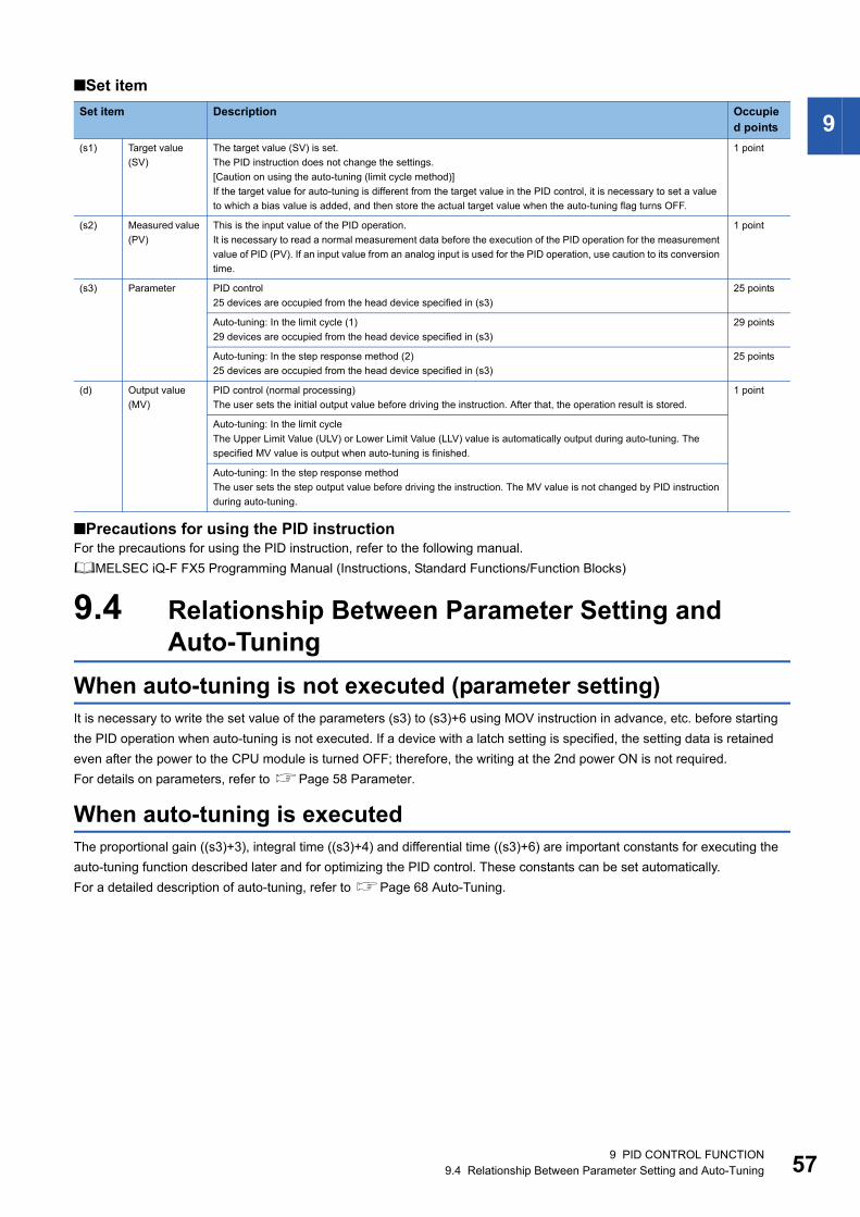
9 PID CONTROL FUNCTION
9.4 Relationship Between Parameter Setting and Auto-Tuning 57
9
■Set item
■Precautions for using the PID instructionFor the precautions for using the PID instruction, refer to the following manual.
MELSEC iQ-F FX5 Programming Manual (Instructions, Standard Functions/Function Blocks)
9.4 Relationship Between Parameter Setting and Auto-Tuning
When auto-tuning is not executed (parameter setting)
It is necessary to write the set value of the parameters (s3) to (s3)+6 using MOV instruction in advance, etc. before starting
the PID operation when auto-tuning is not executed. If a device with a latch setting is specified, the setting data is retained
even after the power to the CPU module is turned OFF; therefore, the writing at the 2nd power ON is not required.
For details on parameters, refer to Page 58 Parameter.
When auto-tuning is executed
The proportional gain ((s3)+3), integral time ((s3)+4) and differential time ((s3)+6) are important constants for executing the
auto-tuning function described later and for optimizing the PID control. These constants can be set automatically.
For a detailed description of auto-tuning, refer to Page 68 Auto-Tuning.
Set item Description Occupie
d points
(s1) Target value
(SV)
The target value (SV) is set.
The PID instruction does not change the settings.
[Caution on using the auto-tuning (limit cycle method)]
If the target value for auto-tuning is different from the target value in the PID control, it is necessary to set a value
to which a bias value is added, and then store the actual target value when the auto-tuning flag turns OFF.
1 point
(s2) Measured value
(PV)
This is the input value of the PID operation.
It is necessary to read a normal measurement data before the execution of the PID operation for the measurement
value of PID (PV). If an input value from an analog input is used for the PID operation, use caution to its conversion
time.
1 point
(s3) Parameter PID control
25 devices are occupied from the head device specified in (s3)
25 points
Auto-tuning: In the limit cycle (1)
29 devices are occupied from the head device specified in (s3)
29 points
Auto-tuning: In the step response method (2)
25 devices are occupied from the head device specified in (s3)
25 points
(d) Output value
(MV)
PID control (normal processing)
The user sets the initial output value before driving the instruction. After that, the operation result is stored.
1 point
Auto-tuning: In the limit cycle
The Upper Limit Value (ULV) or Lower Limit Value (LLV) value is automatically output during auto-tuning. The
specified MV value is output when auto-tuning is finished.
Auto-tuning: In the step response method
The user sets the step output value before driving the instruction. The MV value is not changed by PID instruction
during auto-tuning.
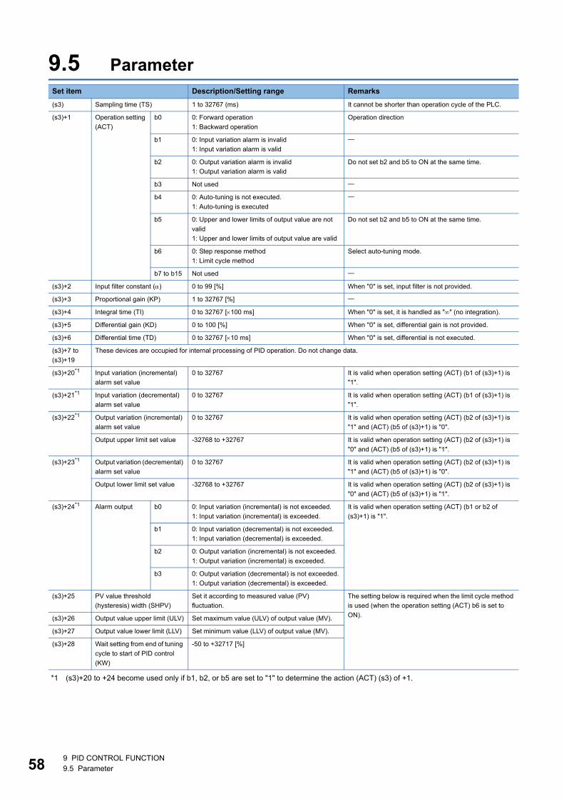
589 PID CONTROL FUNCTION
9.5 Parameter
9.5 Parameter
*1 (s3)+20 to +24 become used only if b1, b2, or b5 are set to "1" to determine the action (ACT) (s3) of +1.
Set item Description/Setting range Remarks
(s3) Sampling time (TS) 1 to 32767 (ms) It cannot be shorter than operation cycle of the PLC.
(s3)+1 Operation setting
(ACT)
b0 0: Forward operation
1: Backward operation
Operation direction
b1 0: Input variation alarm is invalid
1: Input variation alarm is valid
b2 0: Output variation alarm is invalid
1: Output variation alarm is valid
Do not set b2 and b5 to ON at the same time.
b3 Not used
b4 0: Auto-tuning is not executed.
1: Auto-tuning is executed
b5 0: Upper and lower limits of output value are not
valid
1: Upper and lower limits of output value are valid
Do not set b2 and b5 to ON at the same time.
b6 0: Step response method
1: Limit cycle method
Select auto-tuning mode.
b7 to b15 Not used
(s3)+2 Input filter constant () 0 to 99 [%] When "0" is set, input filter is not provided.
(s3)+3 Proportional gain (KP) 1 to 32767 [%]
(s3)+4 Integral time (TI) 0 to 32767 [100 ms] When "0" is set, it is handled as "" (no integration).
(s3)+5 Differential gain (KD) 0 to 100 [%] When "0" is set, differential gain is not provided.
(s3)+6 Differential time (TD) 0 to 32767 [10 ms] When "0" is set, differential is not executed.
(s3)+7 to
(s3)+19
These devices are occupied for internal processing of PID operation. Do not change data.
(s3)+20*1 Input variation (incremental)
alarm set value
0 to 32767 It is valid when operation setting (ACT) (b1 of (s3)+1) is
"1".
(s3)+21*1 Input variation (decremental)
alarm set value
0 to 32767 It is valid when operation setting (ACT) (b1 of (s3)+1) is
"1".
(s3)+22*1 Output variation (incremental)
alarm set value
0 to 32767 It is valid when operation setting (ACT) (b2 of (s3)+1) is
"1" and (ACT) (b5 of (s3)+1) is "0".
Output upper limit set value -32768 to +32767 It is valid when operation setting (ACT) (b2 of (s3)+1) is
"0" and (ACT) (b5 of (s3)+1) is "1".
(s3)+23*1 Output variation (decremental)
alarm set value
0 to 32767 It is valid when operation setting (ACT) (b2 of (s3)+1) is
"1" and (ACT) (b5 of (s3)+1) is "0".
Output lower limit set value -32768 to +32767 It is valid when operation setting (ACT) (b2 of (s3)+1) is
"0" and (ACT) (b5 of (s3)+1) is "1".
(s3)+24*1 Alarm output b0 0: Input variation (incremental) is not exceeded.
1: Input variation (incremental) is exceeded.
It is valid when operation setting (ACT) (b1 or b2 of
(s3)+1) is "1".
b1 0: Input variation (decremental) is not exceeded.
1: Input variation (decremental) is exceeded.
b2 0: Output variation (incremental) is not exceeded.
1: Output variation (incremental) is exceeded.
b3 0: Output variation (decremental) is not exceeded.
1: Output variation (decremental) is exceeded.
(s3)+25 PV value threshold
(hysteresis) width (SHPV)
Set it according to measured value (PV)
fluctuation.
The setting below is required when the limit cycle method
is used (when the operation setting (ACT) b6 is set to
ON).(s3)+26 Output value upper limit (ULV) Set maximum value (ULV) of output value (MV).
(s3)+27 Output value lower limit (LLV) Set minimum value (LLV) of output value (MV).
(s3)+28 Wait setting from end of tuning
cycle to start of PID control
(KW)
-50 to +32717 [%]
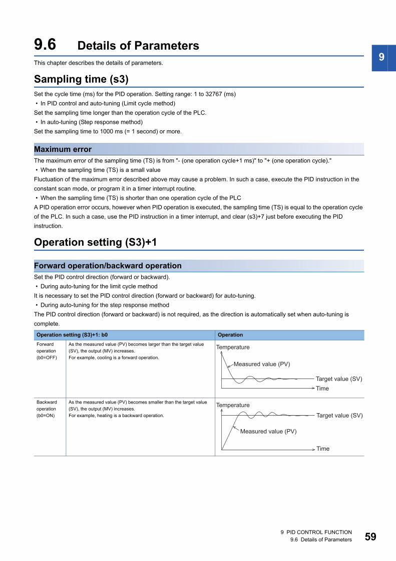
9 PID CONTROL FUNCTION
9.6 Details of Parameters 59
99.6 Details of Parameters
This chapter describes the details of parameters.
Sampling time (s3)
Set the cycle time (ms) for the PID operation. Setting range: 1 to 32767 (ms)
� In PID control and auto-tuning (Limit cycle method)
Set the sampling time longer than the operation cycle of the PLC.
� In auto-tuning (Step response method)
Set the sampling time to 1000 ms (= 1 second) or more.
Maximum error
The maximum error of the sampling time (TS) is from "- (one operation cycle+1 ms)" to "+ (one operation cycle)."
� When the sampling time (TS) is a small value
Fluctuation of the maximum error described above may cause a problem. In such a case, execute the PID instruction in the
constant scan mode, or program it in a timer interrupt routine.
� When the sampling time (TS) is shorter than one operation cycle of the PLC
A PID operation error occurs, however when PID operation is executed, the sampling time (TS) is equal to the operation cycle
of the PLC. In such a case, use the PID instruction in a timer interrupt, and clear (s3)+7 just before executing the PID
instruction.
Operation setting (S3)+1
Forward operation/backward operation
Set the PID control direction (forward or backward).
� During auto-tuning for the limit cycle method
It is necessary to set the PID control direction (forward or backward) for auto-tuning.
� During auto-tuning for the step response method
The PID control direction (forward or backward) is not required, as the direction is automatically set when auto-tuning is
complete.
Operation setting (S3)+1: b0 Operation
Forward
operation
(b0=OFF)
As the measured value (PV) becomes larger than the target value
(SV), the output (MV) increases.
For example, cooling is a forward operation.
Backward
operation
(b0=ON)
As the measured value (PV) becomes smaller than the target value
(SV), the output (MV) increases.
For example, heating is a backward operation.
Temperature
Measured value (PV)
Time
Target value (SV)
Temperature
Measured value (PV)
Time
Target value (SV)
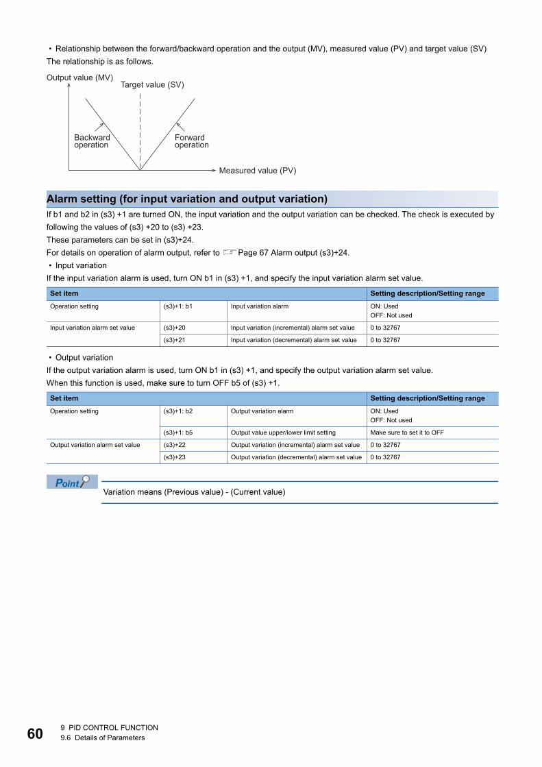
609 PID CONTROL FUNCTION
9.6 Details of Parameters
� Relationship between the forward/backward operation and the output (MV), measured value (PV) and target value (SV)
The relationship is as follows.
Alarm setting (for input variation and output variation)
If b1 and b2 in (s3) +1 are turned ON, the input variation and the output variation can be checked. The check is executed by
following the values of (s3) +20 to (s3) +23.
These parameters can be set in (s3)+24.
For details on operation of alarm output, refer to Page 67 Alarm output (s3)+24.
� Input variation
If the input variation alarm is used, turn ON b1 in (s3) +1, and specify the input variation alarm set value.
� Output variation
If the output variation alarm is used, turn ON b1 in (s3) +1, and specify the output variation alarm set value.
When this function is used, make sure to turn OFF b5 of (s3) +1.
Variation means (Previous value) - (Current value)
Set item Setting description/Setting range
Operation setting (s3)+1: b1 Input variation alarm ON: Used
OFF: Not used
Input variation alarm set value (s3)+20 Input variation (incremental) alarm set value 0 to 32767
(s3)+21 Input variation (decremental) alarm set value 0 to 32767
Set item Setting description/Setting range
Operation setting (s3)+1: b2 Output variation alarm ON: Used
OFF: Not used
(s3)+1: b5 Output value upper/lower limit setting Make sure to set it to OFF
Output variation alarm set value (s3)+22 Output variation (incremental) alarm set value 0 to 32767
(s3)+23 Output variation (decremental) alarm set value 0 to 32767
Measured value (PV)
Output value (MV)Target value (SV)
Backward operation
Forward operation
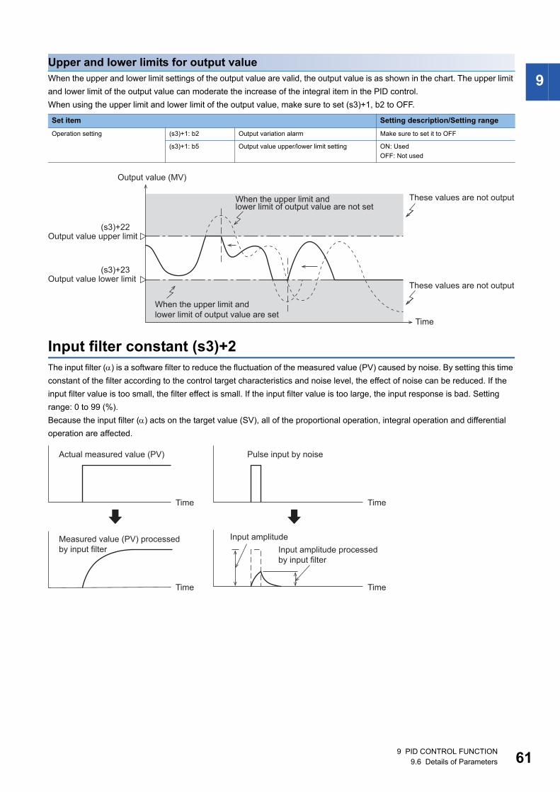
9 PID CONTROL FUNCTION
9.6 Details of Parameters 61
9
Upper and lower limits for output value
When the upper and lower limit settings of the output value are valid, the output value is as shown in the chart. The upper limit
and lower limit of the output value can moderate the increase of the integral item in the PID control.
When using the upper limit and lower limit of the output value, make sure to set (s3)+1, b2 to OFF.
Input filter constant (s3)+2
The input filter () is a software filter to reduce the fluctuation of the measured value (PV) caused by noise. By setting this time
constant of the filter according to the control target characteristics and noise level, the effect of noise can be reduced. If the
input filter value is too small, the filter effect is small. If the input filter value is too large, the input response is bad. Setting
range: 0 to 99 (%).
Because the input filter () acts on the target value (SV), all of the proportional operation, integral operation and differential
operation are affected.
Set item Setting description/Setting range
Operation setting (s3)+1: b2 Output variation alarm Make sure to set it to OFF
(s3)+1: b5 Output value upper/lower limit setting ON: Used
OFF: Not used
Output value upper limit
Output value lower limit
Time
(s3)+22
Output value (MV)
(s3)+23
These values are not output
These values are not output
When the upper limit and
lower limit of output value are set
When the upper limit and lower limit of output value are not set
Measured value (PV) processed
by input filter
Input amplitude
Pulse input by noiseActual measured value (PV)
Time
Time
Time
Time
Input amplitude processed
by input filter
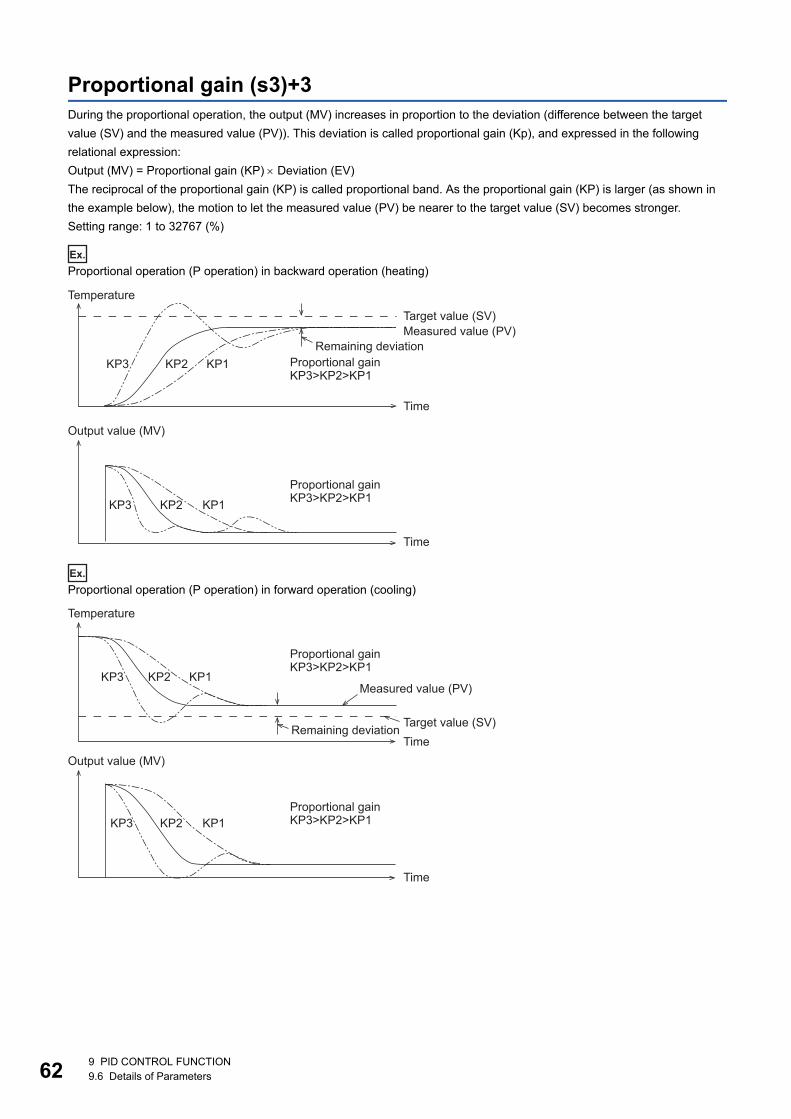
629 PID CONTROL FUNCTION
9.6 Details of Parameters
Proportional gain (s3)+3
During the proportional operation, the output (MV) increases in proportion to the deviation (difference between the target
value (SV) and the measured value (PV)). This deviation is called proportional gain (Kp), and expressed in the following
relational expression:
Output (MV) = Proportional gain (KP) Deviation (EV)
The reciprocal of the proportional gain (KP) is called proportional band. As the proportional gain (KP) is larger (as shown in
the example below), the motion to let the measured value (PV) be nearer to the target value (SV) becomes stronger.
Setting range: 1 to 32767 (%)
Ex.
Proportional operation (P operation) in backward operation (heating)
Ex.
Proportional operation (P operation) in forward operation (cooling)
Output value (MV)
Temperature
Remaining deviation
Proportional gainKP3>KP2>KP1
Proportional gain
Time
Time
Target value (SV)
Measured value (PV)
KP3>KP2>KP1
KP3 KP2 KP1
KP3 KP2 KP1
Output value (MV)
Temperature
Remaining deviation
Proportional gainKP3>KP2>KP1
Proportional gain
Time
Time
Target value (SV)
Measured value (PV)
KP3>KP2>KP1
KP3 KP2 KP1
KP3 KP2 KP1
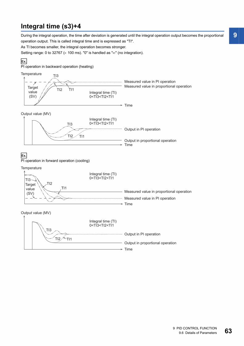
9 PID CONTROL FUNCTION
9.6 Details of Parameters 63
9
Integral time (s3)+4
During the integral operation, the time after deviation is generated until the integral operation output becomes the proportional
operation output. This is called integral time and is expressed as "TI".
As TI becomes smaller, the integral operation becomes stronger.
Setting range: 0 to 32767 ( 100 ms). "0" is handled as "" (no integration).
Ex.
PI operation in backward operation (heating)
Ex.
PI operation in forward operation (cooling)
Output value (MV)
Temperature
Integral time (TI)0<TI3<TI2<TI1
Integral time (TI)
Time
Time
Output in PI operation
Output in proportional operation
Measured value in PI operation
Measured value in proportional operation
0<TI3<TI2<TI1
TI3
TI2 TI1
TI3
TI2 TI1
Target
value
(SV)
Output value (MV)
Temperature
Integral time (TI)0<TI3<TI2<TI1
Integral time (TI)
Time
Time
Output in PI operation
Output in proportional operation
Measured value in PI operation
Measured value in proportional operation
0<TI3<TI2<TI1TI3TI2
TI1
TI3
TI2 TI1
Target
value
(SV)
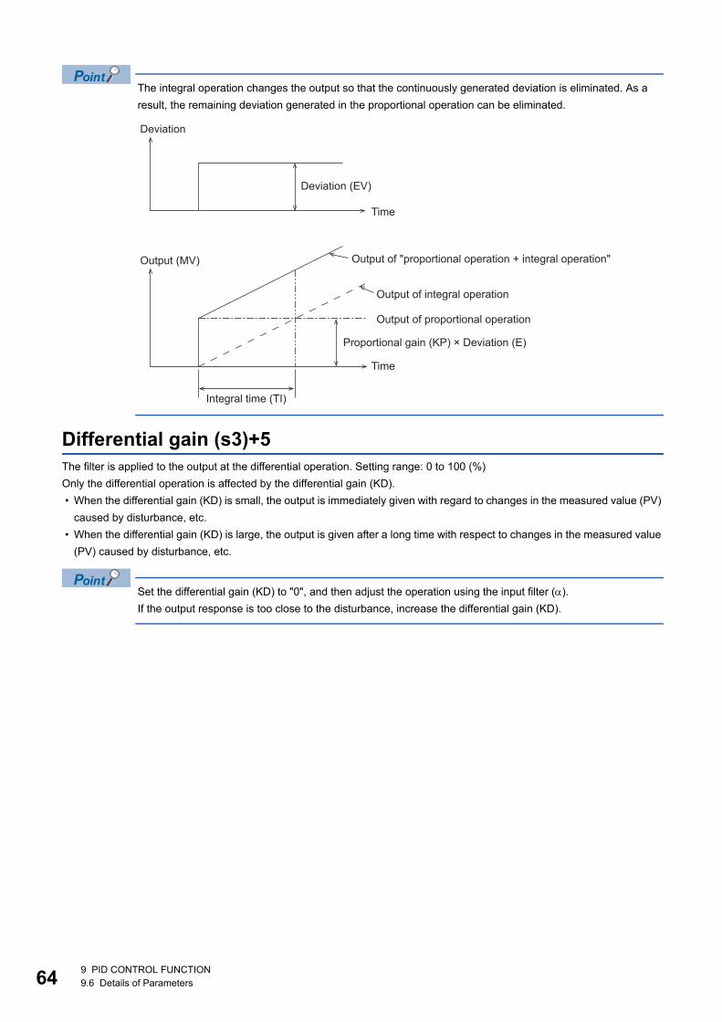
649 PID CONTROL FUNCTION
9.6 Details of Parameters
The integral operation changes the output so that the continuously generated deviation is eliminated. As a
result, the remaining deviation generated in the proportional operation can be eliminated.
Differential gain (s3)+5
The filter is applied to the output at the differential operation. Setting range: 0 to 100 (%)
Only the differential operation is affected by the differential gain (KD).
� When the differential gain (KD) is small, the output is immediately given with regard to changes in the measured value (PV)
caused by disturbance, etc.
� When the differential gain (KD) is large, the output is given after a long time with respect to changes in the measured value
(PV) caused by disturbance, etc.
Set the differential gain (KD) to "0", and then adjust the operation using the input filter ().
If the output response is too close to the disturbance, increase the differential gain (KD).
Deviation
Output (MV)
Deviation (EV)
Time
Time
Output of "proportional operation + integral operation"
Output of integral operation
Output of proportional operation
Proportional gain (KP) × Deviation (E)
Integral time (TI)
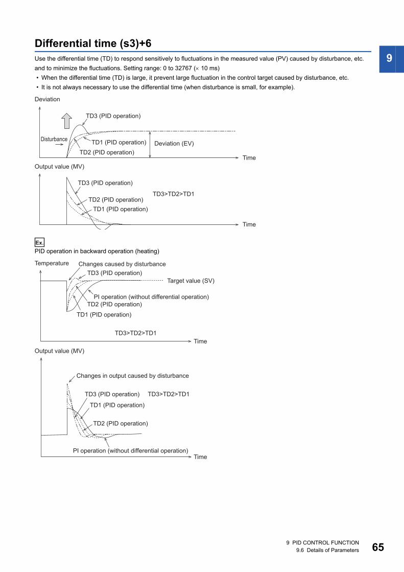
9 PID CONTROL FUNCTION
9.6 Details of Parameters 65
9
Differential time (s3)+6
Use the differential time (TD) to respond sensitively to fluctuations in the measured value (PV) caused by disturbance, etc.
and to minimize the fluctuations. Setting range: 0 to 32767 ( 10 ms)
� When the differential time (TD) is large, it prevent large fluctuation in the control target caused by disturbance, etc.
� It is not always necessary to use the differential time (when disturbance is small, for example).
Ex.
PID operation in backward operation (heating)
Output value (MV)
Deviation
DisturbanceDeviation (EV)
Time
Time
TD3>TD2>TD1
TD3 (PID operation)
TD1 (PID operation)
TD2 (PID operation)
TD3 (PID operation)
TD1 (PID operation)
TD2 (PID operation)
Output value (MV)
Temperature
Target value (SV)
Time
Time
TD3>TD2>TD1
TD3>TD2>TD1
TD3 (PID operation)
PI operation (without differential operation)
PI operation (without differential operation)
TD2 (PID operation)
TD3 (PID operation)
Changes in output caused by disturbance
Changes caused by disturbance
TD1 (PID operation)
TD1 (PID operation)
TD2 (PID operation)
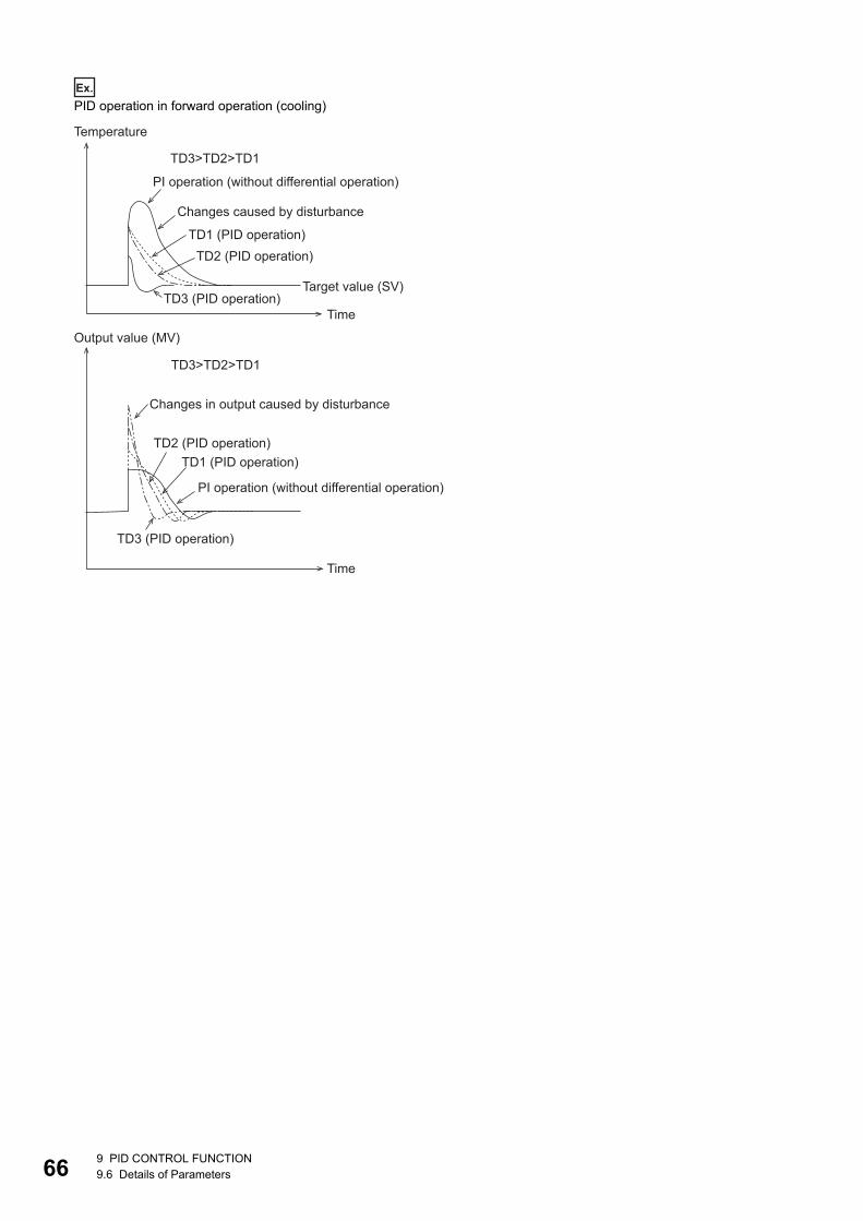
669 PID CONTROL FUNCTION
9.6 Details of Parameters
Ex.
PID operation in forward operation (cooling)
Output value (MV)
Temperature
Target value (SV)
Time
Time
TD3>TD2>TD1
TD3>TD2>TD1
TD3 (PID operation)
PI operation (without differential operation)
PI operation (without differential operation)
TD2 (PID operation)
TD3 (PID operation)
Changes in output caused by disturbance
Changes caused by disturbance
TD1 (PID operation)
TD1 (PID operation)
TD2 (PID operation)
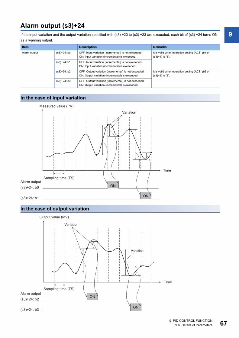
9 PID CONTROL FUNCTION
9.6 Details of Parameters 67
9
Alarm output (s3)+24
If the input variation and the output variation specified with (s3) +20 to (s3) +23 are exceeded, each bit of (s3) +24 turns ON
as a warning output.
In the case of input variation
In the case of output variation
Item Description Remarks
Alarm output (s3)+24: b0 OFF: Input variation (incremental) is not exceeded.
ON: Input variation (incremental) is exceeded.
It is valid when operation setting (ACT) (b1 of
(s3)+1) is "1".
(s3)+24: b1 OFF: Input variation (incremental) is not exceeded.
ON: Input variation (incremental) is exceeded.
(s3)+24: b2 OFF: Output variation (incremental) is not exceeded.
ON: Output variation (incremental) is exceeded.
It is valid when operation setting (ACT) (b2 of
(s3)+1) is "1".
(s3)+24: b3 OFF: Output variation (incremental) is not exceeded.
ON: Output variation (incremental) is exceeded.
Measured value (PV)
Variation
Time
Sampling time (TS)
ON
ON
Alarm output
(s3)+24: b1
(s3)+24: b0
Output value (MV)
Variation
Variation
Time
Sampling time (TS)
ON
ON
Alarm output
(s3)+24: b3
(s3)+24: b2
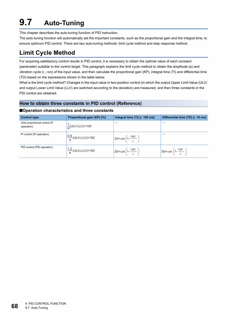
689 PID CONTROL FUNCTION
9.7 Auto-Tuning
9.7 Auto-Tuning
This chapter describes the auto-tuning function of PID instruction.
The auto-tuning function will automatically set the important constants, such as the proportional gain and the integral time, to
ensure optimum PID control. There are two auto-tuning methods: limit cycle method and step response method.
Limit Cycle Method
For acquiring satisfactory control results in PID control, it is necessary to obtain the optimal value of each constant
(parameter) suitable to the control target. This paragraph explains the limit cycle method to obtain the amplitude (a) and
vibration cycle (, on) of the input value, and then calculate the proportional gain (KP), integral time (TI) and differential time
(TD) based on the expressions shown in the table below.
What is the limit cycle method? Changes in the input value in two-position control (in which the output Upper Limit Value (ULV)
and output Lower Limit Value (LLV) are switched according to the deviation) are measured, and then three constants in the
PID control are obtained.
How to obtain three constants in PID control (Reference)
■Operation characteristics and three constants
Control type Proportional gain (KP) [%] Integral time (TI) [ 100 ms] Differential time (TD) [ 10 ms]
Only proportional control (P
operation)
PI control (PI operation)
PID control (PID operation)
a1
(ULV-LLV)×100
a0.9
(ULV-LLV)×100on
1-33×on
a1.2
(ULV-LLV)×100on
1-20×onon
1-50×on
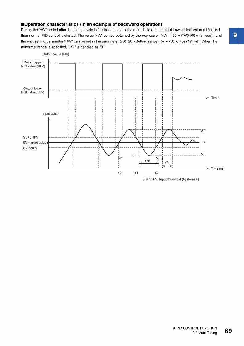
9 PID CONTROL FUNCTION
9.7 Auto-Tuning 69
9
■Operation characteristics (in an example of backward operation)During the "W" period after the tuning cycle is finished, the output value is held at the output Lower Limit Value (LLV), and
then normal PID control is started. The value "W" can be obtained by the expression "W = (50 + KW)/100 ( - on)", and
the wait setting parameter "KW" can be set in the parameter (s3)+28. (Setting range: Kw = -50 to +32717 [%]) (When the
abnormal range is specified, "W" is handled as "0")
Input value
Time (s)
Output value (MV)
a
on
SV (target value)
SV+SHPV
SV-SHPV
0 1 2
W
Time
SHPV: PV Input threshold (hysteresis)
Output lower
limit value (LLV)
Output upper
limit value (ULV)
709 PID CONTROL FUNCTION
9.7 Auto-Tuning
Parameters set in limit cycle method
The parameters specified in the limit cycle method are shown below.
Auto-tuning procedure
1. Set forward or backward operation
Set the operation direction flag (b0) in the operation setting parameter (ACT) (s3)+1.
2. Select the auto-tuning method (limit cycle method)
Set the auto-tuning method to ON (b6) in the operation setting parameter (ACT) (s3)+1. (When bit 6 is set to OFF, the step
response method is selected.)
3. Set the auto-tuning execution flag to ON
Set the auto-tuning execution flag to ON (b4) in the operation setting parameter (ACT) (s3)+1.
4. Set the input filter
Set the input filter in the operation setting parameter (ACT) (s3)+2.
5. Set the sampling time
Set the sampling time (s3).
6. Set the Upper Limit Value (ULV)
Set the Upper Limit Value (ULV) of the output value (MV) in the operation setting parameter (ACT) (s3)+26.
7. Set the Lower Limit Value (LLV)
Set the Lower Limit Value (LLV) of the output value (MV) in the operation setting parameter (ACT) (s3)+27.
8. Set the threshold (hysteresis) (SHPV)
Set the threshold (hysteresis) width (SHPV) in the operation setting parameter (ACT) (s3)+25.
9. Set the target value (SV)
Set the target value (SV) in PID instruction.
10.Set the PID instruction command input ON to start auto-tuning
Auto-tuning is executed according to the measured value (PV).
When auto-tuning is completed, the auto-tuning flag (b4 and b6) turns OFF in the operation setting parameter (ACT) (s3)+1.
Parameter Setting position
Proportional gain (KP) (s3)+3
Integral time (TI) (s3)+4
Differential time (TD) (s3)+6
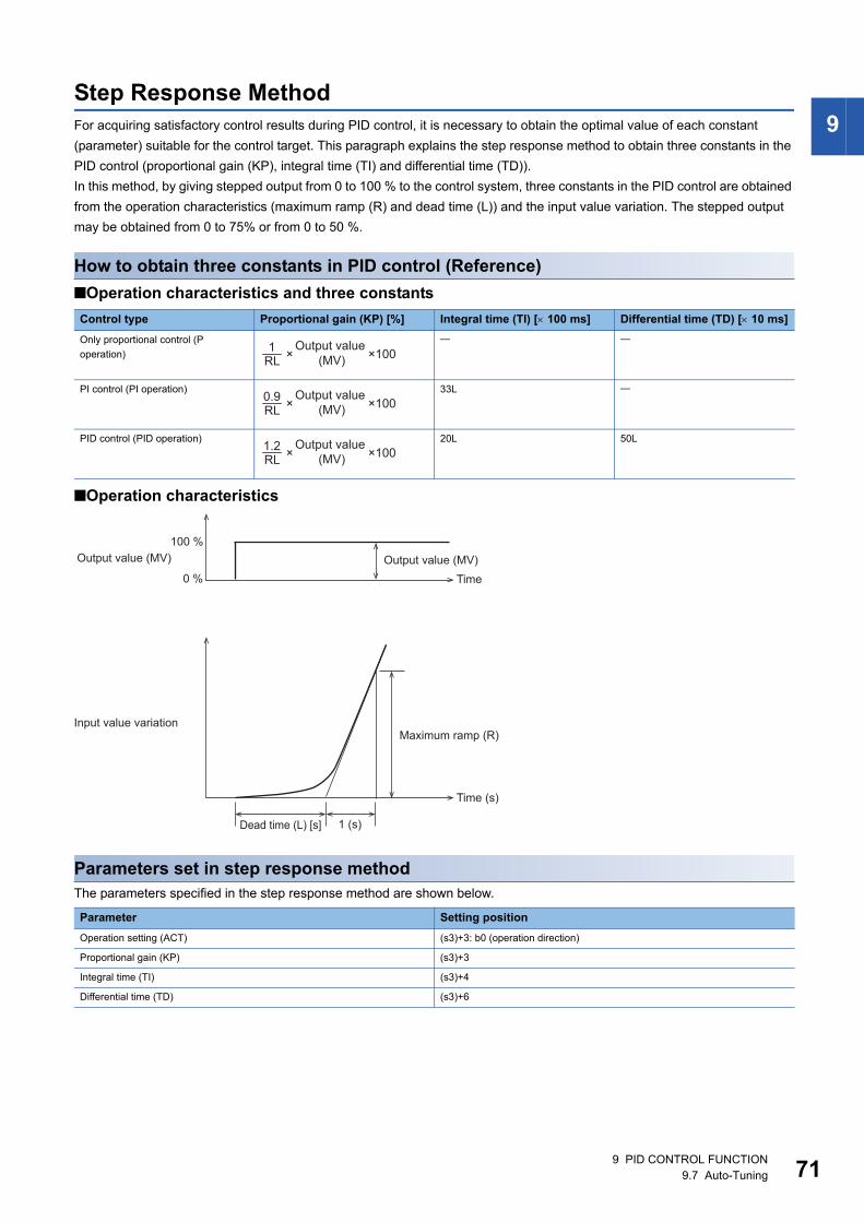
9 PID CONTROL FUNCTION
9.7 Auto-Tuning 71
9
Step Response Method
For acquiring satisfactory control results during PID control, it is necessary to obtain the optimal value of each constant
(parameter) suitable for the control target. This paragraph explains the step response method to obtain three constants in the
PID control (proportional gain (KP), integral time (TI) and differential time (TD)).
In this method, by giving stepped output from 0 to 100 % to the control system, three constants in the PID control are obtained
from the operation characteristics (maximum ramp (R) and dead time (L)) and the input value variation. The stepped output
may be obtained from 0 to 75% or from 0 to 50 %.
How to obtain three constants in PID control (Reference)
■Operation characteristics and three constants
■Operation characteristics
Parameters set in step response method
The parameters specified in the step response method are shown below.
Control type Proportional gain (KP) [%] Integral time (TI) [ 100 ms] Differential time (TD) [ 10 ms]
Only proportional control (P
operation)
PI control (PI operation) 33L
PID control (PID operation) 20L 50L
Parameter Setting position
Operation setting (ACT) (s3)+3: b0 (operation direction)
Proportional gain (KP) (s3)+3
Integral time (TI) (s3)+4
Differential time (TD) (s3)+6
RL1 Output value
(MV)× ×100
RL0.9 Output value
(MV)× ×100
RL1.2 Output value
(MV)× ×100
0 %
100 %
Output value (MV) Output value (MV)
Time
Dead time (L) [s]
Time (s)
1 (s)
Maximum ramp (R)Input value variation
729 PID CONTROL FUNCTION
9.7 Auto-Tuning
Auto-tuning procedure
1. Transferring the output value for auto-tuning to the output value (d)
Set the output value for auto-tuning to the maximum available output value multiplied by 0.5 to 1 for the output equipment.
2. Setting the parameter (s3), target value (SV), etc. that cannot be set in autotuning according to the system
3. Setting to ON b4 of (s3)+1 (operation setting ACT) to start auto-tuning
When the variation from the measured value at the start of auto-tuning to the target value reaches 1/3 or more, auto-tuning is
completed. And bit 4 of (s3)+1 (operation setting ACT) is automatically set to OFF.
Start auto-tuning while the system is stable.
If the system is unstable when auto-tuning is started, auto-tuning may not be executed normally.
Cautions on auto-tuning setting
Note that auto-tuning may not be executed normally if the cautions described below are not followed
� Difference between the target value (SV) and the measured value (PV)
If the difference between the target value (SV) and the measured value (PV) is less than 150 when autotuning is started, auto-
tuning is not executed normally. Accordingly, if the difference is less than 150, set the target value for auto-tuning. Set the
target value again when auto-tuning is completed.
� Sampling time (TS)
Make sure the sampling time is set for auto-tuning to 1 second (1000 ms) or more. It is recommended that the sampling time
is set to that it is considerably longer than the output change cycle.
Cautions on auto-tuning execution
■Program countermeasures when the input value (PV) does not changeWhen the input value (PV) does not change normally due to factors such as wire breakage in an analog input line, auto-tuning
is not finished. Detect and avoid such occurrences by introducing a sequence to monitor the input value or the elapsed time
from the start of auto-tuning.
9 PID CONTROL FUNCTION
9.8 Examples of Program 73
99.8 Examples of Program
System configuration example
An example of the system configuration when the PID control function is used is shown below.
System configuration
Operation of the electric heater
■During PID control
■During auto-tuning
Program examples
Program example Description Reference
Program example 1 This is an example of the sample program for PID control. Page 74
Program example 2 This is an example of the sample program for auto tuning (limit cycle method). Page 76
Program example 3 This is an example of the sample program for auto tuning (step response method). Page 78
Program example 4 This is an example of the sample program for auto tuning (limit cycle method) + PID
control.
Page 80
Program example 5 This is an example of the sample program for auto tuning (step response method) + PID
control.
Page 82
V1+ V2-
AD
V- 0V
COM0 Y0
Electric heater
Temperature chamber
Resistance temperature sensor(Pt100 sensor)
X10: Auto-tuning commandX11: PID control command
Resistance temperature sensor converterM2RS-44-R/UL
10V 0V
1 4 5
Error indication
24 V DC power supply
FX5U-32MT/ES
Y1
24V X10 X11
Power supply
D502×1 ms <ON duration>
OFF ON ON ON ON ON
2 sec (2000 ms) <cycle>
2 sec (2000 ms) 2 sec (2000 ms)
1.8 sec (1800 ms) 1.8 sec (1800 ms) 1.8 sec (1800 ms)
2 sec (2000 ms) 2 sec (2000 ms) 2 sec (2000 ms)
749 PID CONTROL FUNCTION
9.8 Examples of Program
Program example 1
This is an example of the sample program for PID control.
Use device
The content of the devices used for the program is as follows.
: This is an item not occupied.
*1 The setting is always necessary.
*2 When CH1 is used.
Item Device Setting value
During auto-tuning During PID control
Target value (SV)*1 (s1) D500 Not used 5000 (50.0)
Measured value (PV)*1 (s2) SD6022 Not used According to input value*2
Parameter Sampling time (TS)*1 (s3) D510 Not used 500 (500 ms)
Operation setting
(ACT)
Operation direction*1 (s3)+1 b0 D511.0 Not used 1 (Backward operation)
Input variation alarm (s3)+1 b1 D511.1 Not used 0 (Alarm is not provided)
Output variation alarm (s3)+1 b2 D511.2 Not used 0 (Alarm is not provided)
Auto-tuning (s3)+1 b4 D511.4 Not used 0 (AT is not provided)
Upper and lower limits of
output value
(s3)+1 b5 D511.5 Not used 1 (Setting is provided)
Select auto-tuning mode (s3)+1 b6 D511.6 Not used Not used
Input filter constant () (s3)+2 D512 Not used 0 (Input filter is not provided)
Proportional gain (KP)*1 (s3)+3 D513 Not used 3000 (3000 %)
Integral time (TI)*1 (s3)+4 D514 Not used 2000 (2000100 ms)
Differential gain (KD) (s3)+5 D515 Not used 0 (Differential gain is not
provided)
Differential time (TD)*1 (s3)+6 D516 Not used 5000 (500010 ms)
Input variation (incremental) alarm set value (s3)+20 D530 Not used Not used
Input variation (decremental) alarm set value (s3)+21 D531 Not used Not used
Output variation (incremental) alarm set value
Output upper limit set value
(s3)+22 D532 Not used 2000 (2 second)
Output variation (decremental) alarm set value
Output lower limit set value
(s3)+23 D533 Not used 0 (0 second)
Alarm output Input variation (incremental) is
exceeded
(s3)+24 b0 D534.0 Not used Not used
Input variation (decremental)
is exceeded
(s3)+24 b1 D534.1 Not used Not used
Output variation (incremental)
is exceeded
(s3)+24 b2 D534.2 Not used Not used
Output variation (decremental)
is exceeded
(s3)+24 b3 D534.3 Not used Not used
PV value threshold (hysteresis) width (SHPV) (s3)+25 D535
Output value upper limit (ULV) (s3)+26 D536
Output value lower limit (LLV) (s3)+27 D537
Wait setting from end of tuning cycle to start of PID
control (KW)
(s3)+28 D538
Output value (MV)*1 (d) D502 Not used According to operation
9 PID CONTROL FUNCTION
9.8 Examples of Program 75
9
Program
OUTHS ST0 K2000
MOV
SM402
Initial pulse
SM402
Initial pulse
SM402
Initial pulse
X011
PID control is started
M3
PID operation is executed
ST0
Heater operation cycle
M3
PID operation is executed
M3
PID operation is executed
ST0<D502
X011
PID control is started
MOV
MOV
MOV
MOV
MOV
MOV
SD6022
K5000
K500
SET
SET
K2000
K0
K3000
K2000
K5000
RST
RST
D510PID
< ST0 D502
D500
RST
D500 The target value is set to 50°C
The sampling time is set to 500 ms
The operation direction is set to backward operation
The upper and lower limits of output value is set to valid
The output value upper limit is set to ON for 2 sec. PID instruction initial setting
Built-in analog monitor CH1: SD6022 CH2: SD6062
0: Enable1: Disable
Heater output control
The output value lower limit is set to ON for 0 sec.
The proportional gain is set to 3000 %
The integral time is set to 2000×100ms
The differential time is set to 5000×100ms
The built-in analog is set to used CH. CH1: SM6021 CH2: SM6061
The PID output is initialized
PID instruction drive
PID operation is executed
The heater operation cycle is set to 2 sec
Preset
Heater output
D510
D511.0
D511.5
D532
D533
D513
D514
D516
SM6021
D502
D502
M3
ST0
Y1
END
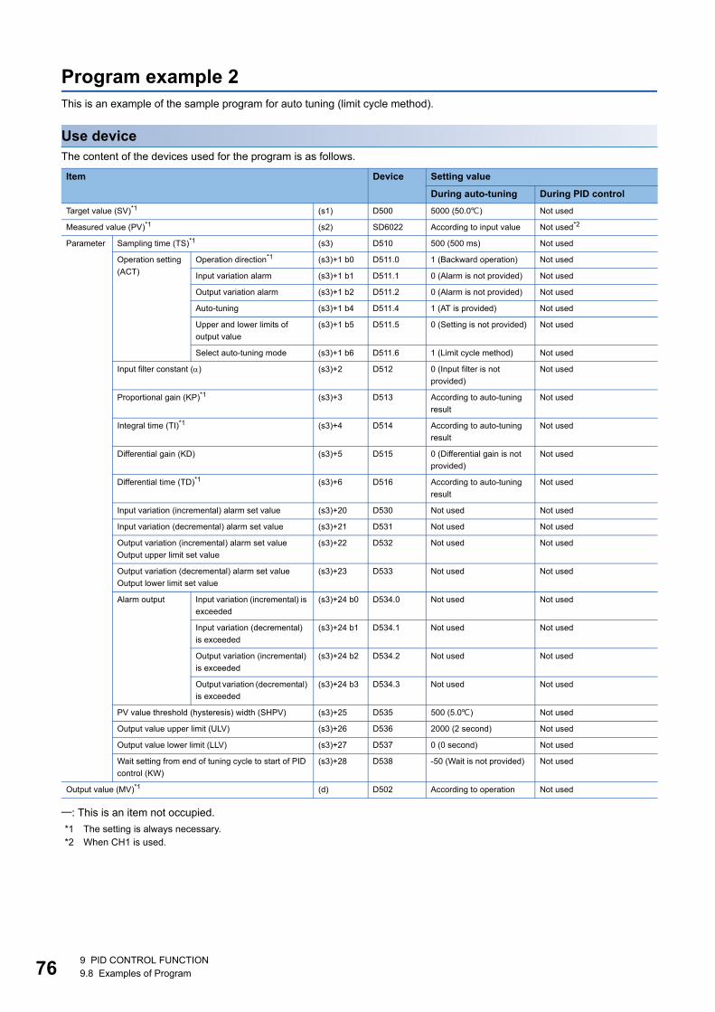
769 PID CONTROL FUNCTION
9.8 Examples of Program
Program example 2
This is an example of the sample program for auto tuning (limit cycle method).
Use device
The content of the devices used for the program is as follows.
: This is an item not occupied.
*1 The setting is always necessary.
*2 When CH1 is used.
Item Device Setting value
During auto-tuning During PID control
Target value (SV)*1 (s1) D500 5000 (50.0) Not used
Measured value (PV)*1 (s2) SD6022 According to input value Not used*2
Parameter Sampling time (TS)*1 (s3) D510 500 (500 ms) Not used
Operation setting
(ACT)
Operation direction*1 (s3)+1 b0 D511.0 1 (Backward operation) Not used
Input variation alarm (s3)+1 b1 D511.1 0 (Alarm is not provided) Not used
Output variation alarm (s3)+1 b2 D511.2 0 (Alarm is not provided) Not used
Auto-tuning (s3)+1 b4 D511.4 1 (AT is provided) Not used
Upper and lower limits of
output value
(s3)+1 b5 D511.5 0 (Setting is not provided) Not used
Select auto-tuning mode (s3)+1 b6 D511.6 1 (Limit cycle method) Not used
Input filter constant () (s3)+2 D512 0 (Input filter is not
provided)
Not used
Proportional gain (KP)*1 (s3)+3 D513 According to auto-tuning
result
Not used
Integral time (TI)*1 (s3)+4 D514 According to auto-tuning
result
Not used
Differential gain (KD) (s3)+5 D515 0 (Differential gain is not
provided)
Not used
Differential time (TD)*1 (s3)+6 D516 According to auto-tuning
result
Not used
Input variation (incremental) alarm set value (s3)+20 D530 Not used Not used
Input variation (decremental) alarm set value (s3)+21 D531 Not used Not used
Output variation (incremental) alarm set value
Output upper limit set value
(s3)+22 D532 Not used Not used
Output variation (decremental) alarm set value
Output lower limit set value
(s3)+23 D533 Not used Not used
Alarm output Input variation (incremental) is
exceeded
(s3)+24 b0 D534.0 Not used Not used
Input variation (decremental)
is exceeded
(s3)+24 b1 D534.1 Not used Not used
Output variation (incremental)
is exceeded
(s3)+24 b2 D534.2 Not used Not used
Output variation (decremental)
is exceeded
(s3)+24 b3 D534.3 Not used Not used
PV value threshold (hysteresis) width (SHPV) (s3)+25 D535 500 (5.0) Not used
Output value upper limit (ULV) (s3)+26 D536 2000 (2 second) Not used
Output value lower limit (LLV) (s3)+27 D537 0 (0 second) Not used
Wait setting from end of tuning cycle to start of PID
control (KW)
(s3)+28 D538 -50 (Wait is not provided) Not used
Output value (MV)*1 (d) D502 According to operation Not used
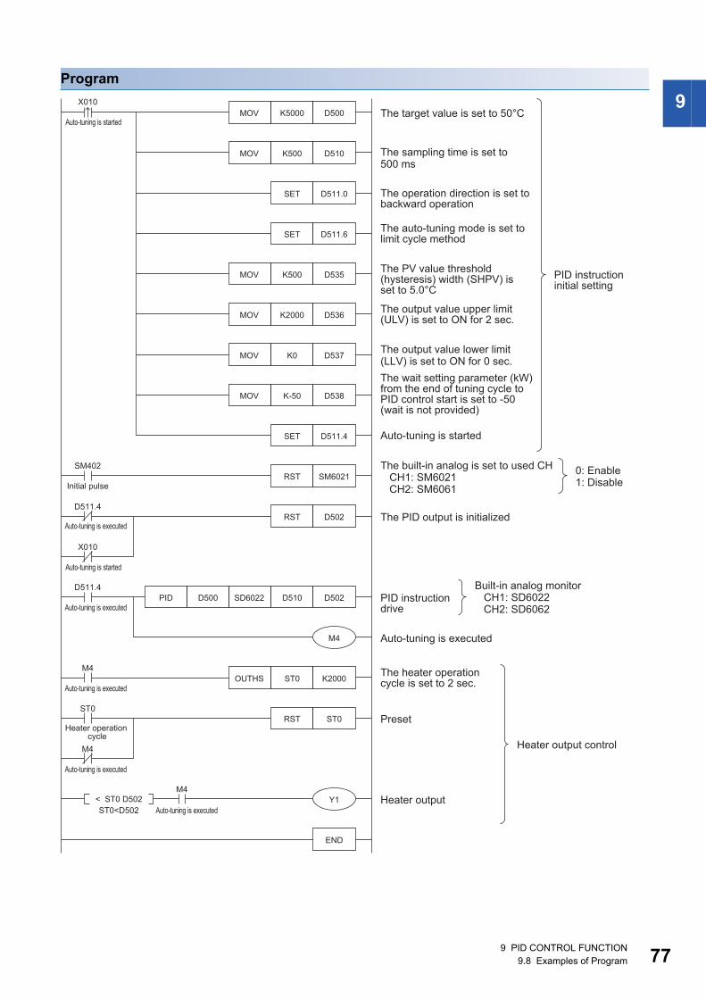
9 PID CONTROL FUNCTION
9.8 Examples of Program 77
9
Program
OUTHS ST0 K2000
MOV
X010
Auto-tuning is started
SM402
Initial pulse
D511.4
Auto-tuning is executed
Auto-tuning is executed
Auto-tuning is executed
Auto-tuning is executed
X010
Auto-tuning is started
M4
ST0
Heater operation cycle
M4
M4
Auto-tuning is executedST0<D502
D511.4
MOV
MOV
MOV
MOV
MOV
SD6022
K5000
K500
SET
SET
K500
K2000
K0
K-50
SET
RST
RST
D510PID
< ST0 D502
D500
RST
D500 The target value is set to 50°C
The sampling time is set to 500 ms
The operation direction is set to backward operation
The auto-tuning mode is set to limit cycle method
The PV value threshold (hysteresis) width (SHPV) is set to 5.0°C
PID instruction initial setting
Built-in analog monitor CH1: SD6022 CH2: SD6062
0: Enable1: Disable
Heater output control
The output value upper limit (ULV) is set to ON for 2 sec.
The output value lower limit (LLV) is set to ON for 0 sec.
The wait setting parameter (kW) from the end of tuning cycle to PID control start is set to -50 (wait is not provided)
Auto-tuning is started
The built-in analog is set to used CH CH1: SM6021 CH2: SM6061
The PID output is initialized
PID instruction drive
Auto-tuning is executed
The heater operation cycle is set to 2 sec.
Preset
Heater output
D510
D511.0
D511.6
D535
D536
D537
D538
D511.4
SM6021
D502
D502
M4
ST0
Y1
END
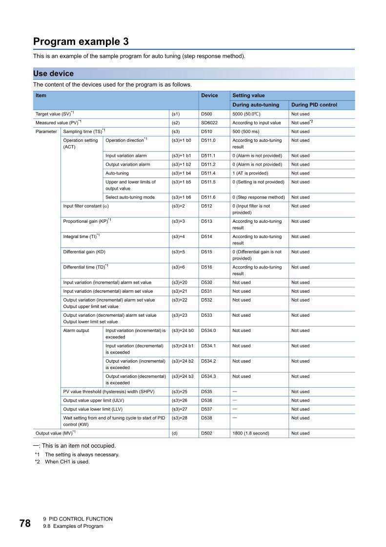
789 PID CONTROL FUNCTION
9.8 Examples of Program
Program example 3
This is an example of the sample program for auto tuning (step response method).
Use device
The content of the devices used for the program is as follows.
: This is an item not occupied.
*1 The setting is always necessary.
*2 When CH1 is used.
Item Device Setting value
During auto-tuning During PID control
Target value (SV)*1 (s1) D500 5000 (50.0) Not used
Measured value (PV)*1 (s2) SD6022 According to input value Not used*2
Parameter Sampling time (TS)*1 (s3) D510 500 (500 ms) Not used
Operation setting
(ACT)
Operation direction*1 (s3)+1 b0 D511.0 According to auto-tuning
result
Not used
Input variation alarm (s3)+1 b1 D511.1 0 (Alarm is not provided) Not used
Output variation alarm (s3)+1 b2 D511.2 0 (Alarm is not provided) Not used
Auto-tuning (s3)+1 b4 D511.4 1 (AT is provided) Not used
Upper and lower limits of
output value
(s3)+1 b5 D511.5 0 (Setting is not provided) Not used
Select auto-tuning mode (s3)+1 b6 D511.6 0 (Step response method) Not used
Input filter constant () (s3)+2 D512 0 (Input filter is not
provided)
Not used
Proportional gain (KP)*1 (s3)+3 D513 According to auto-tuning
result
Not used
Integral time (TI)*1 (s3)+4 D514 According to auto-tuning
result
Not used
Differential gain (KD) (s3)+5 D515 0 (Differential gain is not
provided)
Not used
Differential time (TD)*1 (s3)+6 D516 According to auto-tuning
result
Not used
Input variation (incremental) alarm set value (s3)+20 D530 Not used Not used
Input variation (decremental) alarm set value (s3)+21 D531 Not used Not used
Output variation (incremental) alarm set value
Output upper limit set value
(s3)+22 D532 Not used Not used
Output variation (decremental) alarm set value
Output lower limit set value
(s3)+23 D533 Not used Not used
Alarm output Input variation (incremental) is
exceeded
(s3)+24 b0 D534.0 Not used Not used
Input variation (decremental)
is exceeded
(s3)+24 b1 D534.1 Not used Not used
Output variation (incremental)
is exceeded
(s3)+24 b2 D534.2 Not used Not used
Output variation (decremental)
is exceeded
(s3)+24 b3 D534.3 Not used Not used
PV value threshold (hysteresis) width (SHPV) (s3)+25 D535 Not used
Output value upper limit (ULV) (s3)+26 D536 Not used
Output value lower limit (LLV) (s3)+27 D537 Not used
Wait setting from end of tuning cycle to start of PID
control (KW)
(s3)+28 D538 Not used
Output value (MV)*1 (d) D502 1800 (1.8 second) Not used
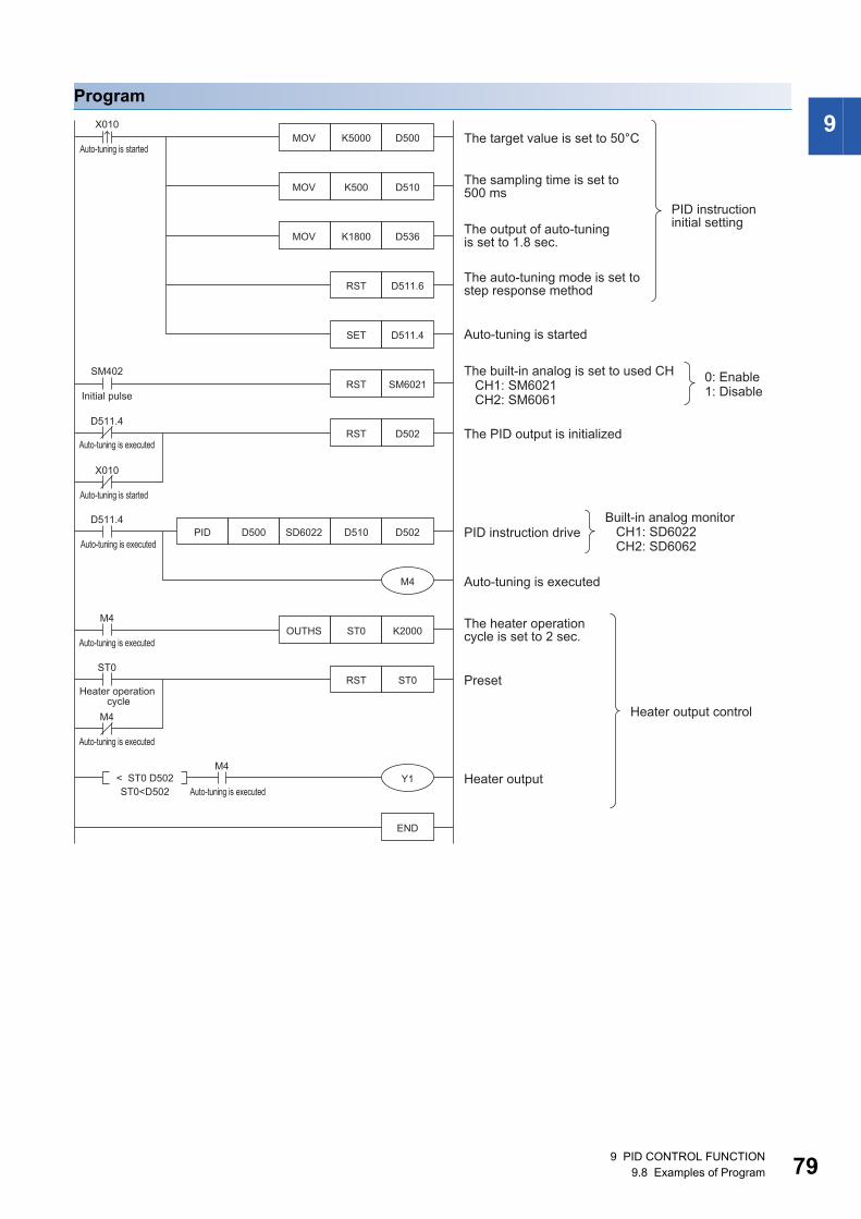
9 PID CONTROL FUNCTION
9.8 Examples of Program 79
9
Program
OUTHS ST0 K2000
MOV
X010
Auto-tuning is started
SM402
Initial pulse
D511.4
Auto-tuning is executed
Auto-tuning is executed
Auto-tuning is executed
Auto-tuning is executed
X010
Auto-tuning is started
M4
ST0
Heater operation cycle
M4
M4
Auto-tuning is executedST0<D502
D511.4
MOV
MOV
SD6022
K5000
K500
K1800
RST
SET
RST
RST
D510PID
< ST0 D502
D500
RST
D500 The target value is set to 50°C
The sampling time is set to 500 ms
The output of auto-tuning is set to 1.8 sec.
PID instruction initial setting
Built-in analog monitor CH1: SD6022 CH2: SD6062
0: Enable1: Disable
Heater output control
The auto-tuning mode is set to step response method
Auto-tuning is started
The built-in analog is set to used CH CH1: SM6021 CH2: SM6061
The PID output is initialized
PID instruction drive
Auto-tuning is executed
The heater operation cycle is set to 2 sec.
Preset
Heater output
D510
D536
D511.6
D511.4
SM6021
D502
D502
M4
ST0
Y1
END
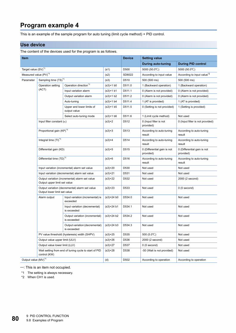
809 PID CONTROL FUNCTION
9.8 Examples of Program
Program example 4
This is an example of the sample program for auto tuning (limit cycle method) + PID control.
Use device
The content of the devices used for the program is as follows.
: This is an item not occupied.
*1 The setting is always necessary.
*2 When CH1 is used.
Item Device Setting value
During auto-tuning During PID control
Target value (SV)*1 (s1) D500 5000 (50.0) 5000 (50.0)
Measured value (PV)*1 (s2) SD6022 According to input value According to input value*2
Parameter Sampling time (TS)*1 (s3) D510 500 (500 ms) 500 (500 ms)
Operation setting
(ACT)
Operation direction*1 (s3)+1 b0 D511.0 1 (Backward operation) 1 (Backward operation)
Input variation alarm (s3)+1 b1 D511.1 0 (Alarm is not provided) 0 (Alarm is not provided)
Output variation alarm (s3)+1 b2 D511.2 0 (Alarm is not provided) 0 (Alarm is not provided)
Auto-tuning (s3)+1 b4 D511.4 1 (AT is provided) 1 (AT is provided)
Upper and lower limits of
output value
(s3)+1 b5 D511.5 0 (Setting is not provided) 1 (Setting is provided)
Select auto-tuning mode (s3)+1 b6 D511.6 1 (Limit cycle method) Not used
Input filter constant () (s3)+2 D512 0 (Input filter is not
provided)
0 (Input filter is not provided)
Proportional gain (KP)*1 (s3)+3 D513 According to auto-tuning
result
According to auto-tuning
result
Integral time (TI)*1 (s3)+4 D514 According to auto-tuning
result
According to auto-tuning
result
Differential gain (KD) (s3)+5 D515 0 (Differential gain is not
provided)
0 (Differential gain is not
provided)
Differential time (TD)*1 (s3)+6 D516 According to auto-tuning
result
According to auto-tuning
result
Input variation (incremental) alarm set value (s3)+20 D530 Not used Not used
Input variation (decremental) alarm set value (s3)+21 D531 Not used Not used
Output variation (incremental) alarm set value
Output upper limit set value
(s3)+22 D532 Not used 2000 (2 second)
Output variation (decremental) alarm set value
Output lower limit set value
(s3)+23 D533 Not used 0 (0 second)
Alarm output Input variation (incremental) is
exceeded
(s3)+24 b0 D534.0 Not used Not used
Input variation (decremental)
is exceeded
(s3)+24 b1 D534.1 Not used Not used
Output variation (incremental)
is exceeded
(s3)+24 b2 D534.2 Not used Not used
Output variation (decremental)
is exceeded
(s3)+24 b3 D534.3 Not used Not used
PV value threshold (hysteresis) width (SHPV) (s3)+25 D535 500 (5.0) Not used
Output value upper limit (ULV) (s3)+26 D536 2000 (2 second) Not used
Output value lower limit (LLV) (s3)+27 D537 0 (0 second) Not used
Wait setting from end of tuning cycle to start of PID
control (KW)
(s3)+28 D538 -50 (Wait is not provided) Not used
Output value (MV)*1 (d) D502 According to operation According to operation
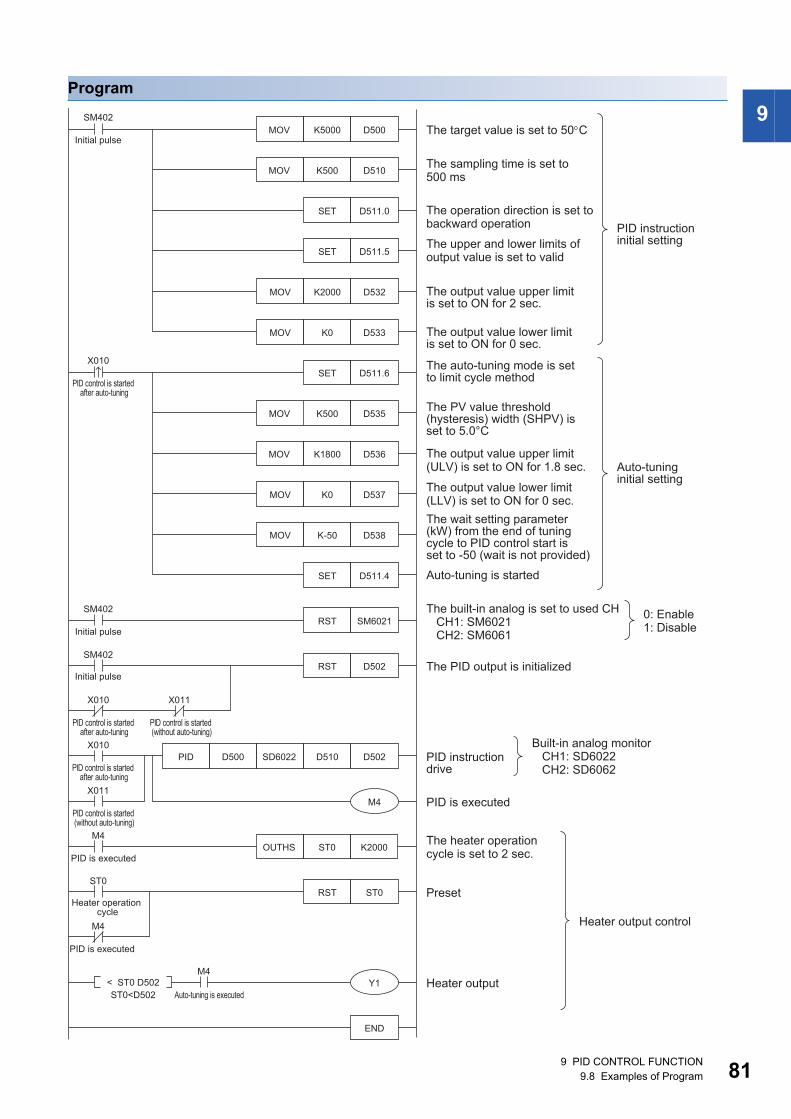
9 PID CONTROL FUNCTION
9.8 Examples of Program 81
9
Program
OUTHS ST0 K2000
MOV
SM402
Initial pulse
SM402
Initial pulse
Initial pulse
SM402
PID control is started after auto-tuning
PID is executed
PID is executed
X010
PID control is started after auto-tuning
X011
PID control is started (without auto-tuning)
M4
ST0
Heater operation cycle
M4
PID control is started (without auto-tuning)
X011
M4
Auto-tuning is executedST0<D502
X010
MOV
SD6022
K5000
K500
SET
SET
K0MOV
RST
RST
D510PID
< ST0 D502
D500
RST
D500 The target value is set to 50C
The sampling time is set to 500 ms
The operation direction is set to backward operation PID instruction
initial setting
Built-in analog monitor CH1: SD6022 CH2: SD6062
0: Enable1: Disable
Heater output control
The upper and lower limits of output value is set to valid
The output value lower limit is set to ON for 0 sec.
The built-in analog is set to used CH CH1: SM6021 CH2: SM6061
The PID output is initialized
PID instruction drive
PID is executed
The heater operation cycle is set to 2 sec.
Preset
Heater output
D510
D511.0
D511.5
K2000MOV The output value upper limit is set to ON for 2 sec.
D532
D533
SM6021
D502
D502
M4
ST0
Y1
END
X010
PID control is started after auto-tuning
MOV
SET
K500
K1800
K0MOV
SET
D511.6The auto-tuning mode is set to limit cycle method
The PV value threshold (hysteresis) width (SHPV) is set to 5.0°C
The output value upper limit (ULV) is set to ON for 1.8 sec. Auto-tuning
initial settingThe output value lower limit (LLV) is set to ON for 0 sec.
Auto-tuning is started
D535
D536
D537
K-50MOV
The wait setting parameter (kW) from the end of tuning cycle to PID control start is set to -50 (wait is not provided)
D538
D511.4
MOV
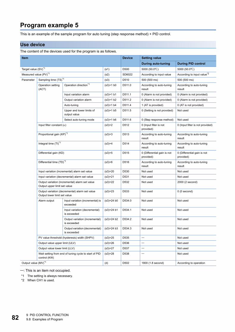
829 PID CONTROL FUNCTION
9.8 Examples of Program
Program example 5
This is an example of the sample program for auto tuning (step response method) + PID control.
Use device
The content of the devices used for the program is as follows.
: This is an item not occupied.
*1 The setting is always necessary.
*2 When CH1 is used.
Item Device Setting value
During auto-tuning During PID control
Target value (SV)*1 (s1) D500 5000 (50.0) 5000 (50.0)
Measured value (PV)*1 (s2) SD6022 According to input value According to input value*2
Parameter Sampling time (TS)*1 (s3) D510 500 (500 ms) 500 (500 ms)
Operation setting
(ACT)
Operation direction*1 (s3)+1 b0 D511.0 According to auto-tuning
result
According to auto-tuning
result
Input variation alarm (s3)+1 b1 D511.1 0 (Alarm is not provided) 0 (Alarm is not provided)
Output variation alarm (s3)+1 b2 D511.2 0 (Alarm is not provided) 0 (Alarm is not provided)
Auto-tuning (s3)+1 b4 D511.4 1 (AT is provided) 0 (AT is not provided)
Upper and lower limits of
output value
(s3)+1 b5 D511.5 0 (Setting is not provided) Not used
Select auto-tuning mode (s3)+1 b6 D511.6 0 (Step response method) Not used
Input filter constant () (s3)+2 D512 0 (Input filter is not
provided)
0 (Input filter is not provided)
Proportional gain (KP)*1 (s3)+3 D513 According to auto-tuning
result
According to auto-tuning
result
Integral time (TI)*1 (s3)+4 D514 According to auto-tuning
result
According to auto-tuning
result
Differential gain (KD) (s3)+5 D515 0 (Differential gain is not
provided)
0 (Differential gain is not
provided)
Differential time (TD)*1 (s3)+6 D516 According to auto-tuning
result
According to auto-tuning
result
Input variation (incremental) alarm set value (s3)+20 D530 Not used Not used
Input variation (decremental) alarm set value (s3)+21 D531 Not used Not used
Output variation (incremental) alarm set value
Output upper limit set value
(s3)+22 D532 Not used 2000 (2 second)
Output variation (decremental) alarm set value
Output lower limit set value
(s3)+23 D533 Not used 0 (0 second)
Alarm output Input variation (incremental) is
exceeded
(s3)+24 b0 D534.0 Not used Not used
Input variation (decremental)
is exceeded
(s3)+24 b1 D534.1 Not used Not used
Output variation (incremental)
is exceeded
(s3)+24 b2 D534.2 Not used Not used
Output variation (decremental)
is exceeded
(s3)+24 b3 D534.3 Not used Not used
PV value threshold (hysteresis) width (SHPV) (s3)+25 D535 Not used
Output value upper limit (ULV) (s3)+26 D536 Not used
Output value lower limit (LLV) (s3)+27 D537 Not used
Wait setting from end of tuning cycle to start of PID
control (KW)
(s3)+28 D538 Not used
Output value (MV)*1 (d) D502 1800 (1.8 second) According to operation
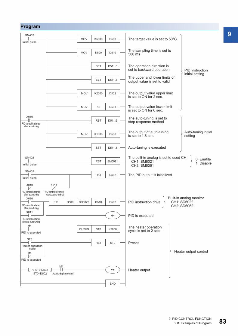
9 PID CONTROL FUNCTION
9.8 Examples of Program 83
9
Program
OUTHS ST0 K2000
MOV
SM402
Initial pulse
SM402
Initial pulse
Initial pulse
SM402
PID control is started after auto-tuning
PID is executed
PID is executed
X010
PID control is started after auto-tuning
X011
PID control is started (without auto-tuning)
M4
ST0
Heater operation cycle
M4
PID control is started (without auto-tuning)
X011
M4
Auto-tuning is executedST0<D502
X010
MOV
SD6022
K5000
K500
SET
SET
K0MOV
RST
RST
D510PID
< ST0 D502
D500
RST
D500 The target value is set to 50°C
The sampling time is set to 500 ms
The operation direction is set to backward operation PID instruction
initial setting
Built-in analog monitor CH1: SD6022 CH2: SD6062
0: Enable1: Disable
Heater output control
The upper and lower limits of output value is set to valid
The output value lower limit is set to ON for 0 sec.
The built-in analog is set to used CH CH1: SM6021 CH2: SM6061
The PID output is initialized
PID instruction drive
PID is executed
The heater operation cycle is set to 2 sec.
Preset
Heater output
D510
D511.0
D511.5
K2000MOV The output value upper limit is set to ON for 2 sec.
D532
D533
SM6021
D502
D502
M4
ST0
Y1
END
X010
PID control is started after auto-tuning
RST
K1800MOV
SET
D511.6The auto-tuning is set to step response method
The output of auto-tuning is set to 1.8 sec.
Auto-tuning initial setting
Auto-tuning is executed
D536
D511.4
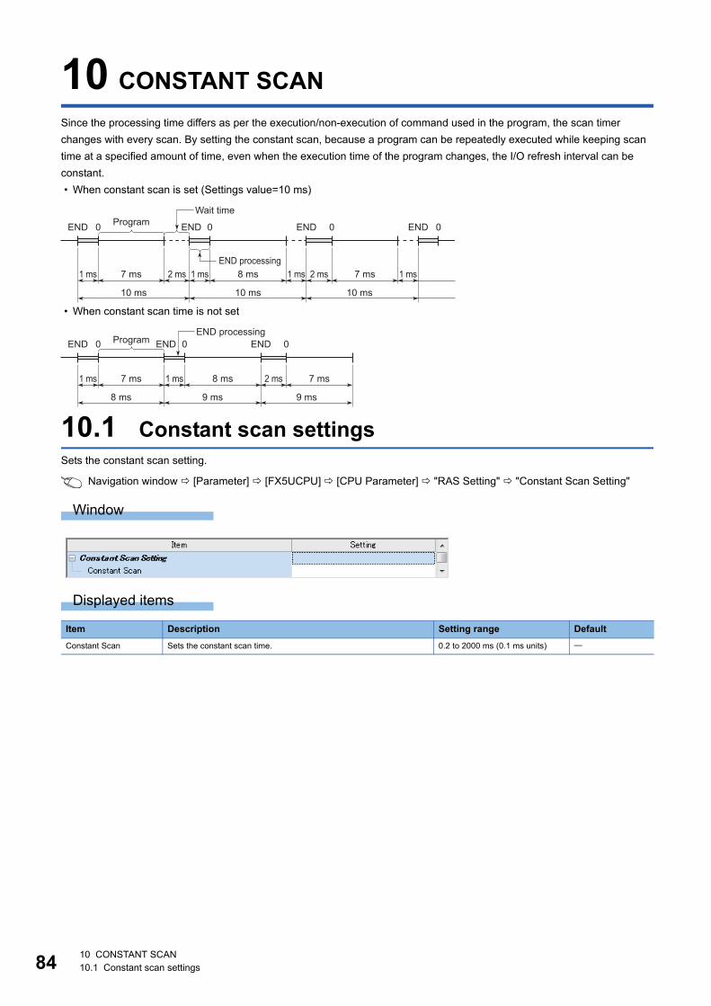
8410 CONSTANT SCAN
10.1 Constant scan settings
10 CONSTANT SCAN
Since the processing time differs as per the execution/non-execution of command used in the program, the scan timer
changes with every scan. By setting the constant scan, because a program can be repeatedly executed while keeping scan
time at a specified amount of time, even when the execution time of the program changes, the I/O refresh interval can be
constant.
� When constant scan is set (Settings value=10 ms)
� When constant scan time is not set
10.1 Constant scan settings
Sets the constant scan setting.
Navigation window [Parameter] [FX5UCPU] [CPU Parameter] "RAS Setting" "Constant Scan Setting"
Window
Displayed items
Item Description Setting range Default
Constant Scan Sets the constant scan time. 0.2 to 2000 ms (0.1 ms units)
END
1 ms 7 ms 2 ms 1 ms 8 ms 1 ms 2 ms 7 ms
10 ms10 ms10 ms
1 ms
END END END0 0 0 0Program
Wait time
END processing
END
1 ms 7 ms 1 ms 8 ms 2 ms 7 ms
9 ms9 ms8 ms
END END0 0 0ProgramEND processing
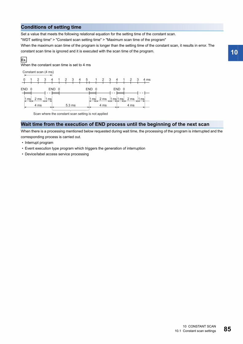
10 CONSTANT SCAN
10.1 Constant scan settings 85
10
Conditions of setting time
Set a value that meets the following relational equation for the setting time of the constant scan.
"WDT setting time" > "Constant scan setting time" > "Maximum scan time of the program"
When the maximum scan time of the program is longer than the setting time of the constant scan, it results in error. The
constant scan time is ignored and it is executed with the scan time of the program.
Ex.
When the constant scan time is set to 4 ms
Wait time from the execution of END process until the beginning of the next scan
When there is a processing mentioned below requested during wait time, the processing of the program is interrupted and the
corresponding process is carried out.
� Interrupt program
� Event execution type program which triggers the generation of interruption
� Device/label access service processing
END 0 END 0 END 0 END 0
1 ms 2 ms 1 ms 1 ms 2 ms 1 ms 1 ms
4 ms4 ms5.3 ms4 ms
0 1 2
Constant scan (4 ms)
3 4 1 2 3 4 5 1 2 3 4 1 2 3 4 ms
1 ms2 ms
Scan where the constant scan setting is not applied
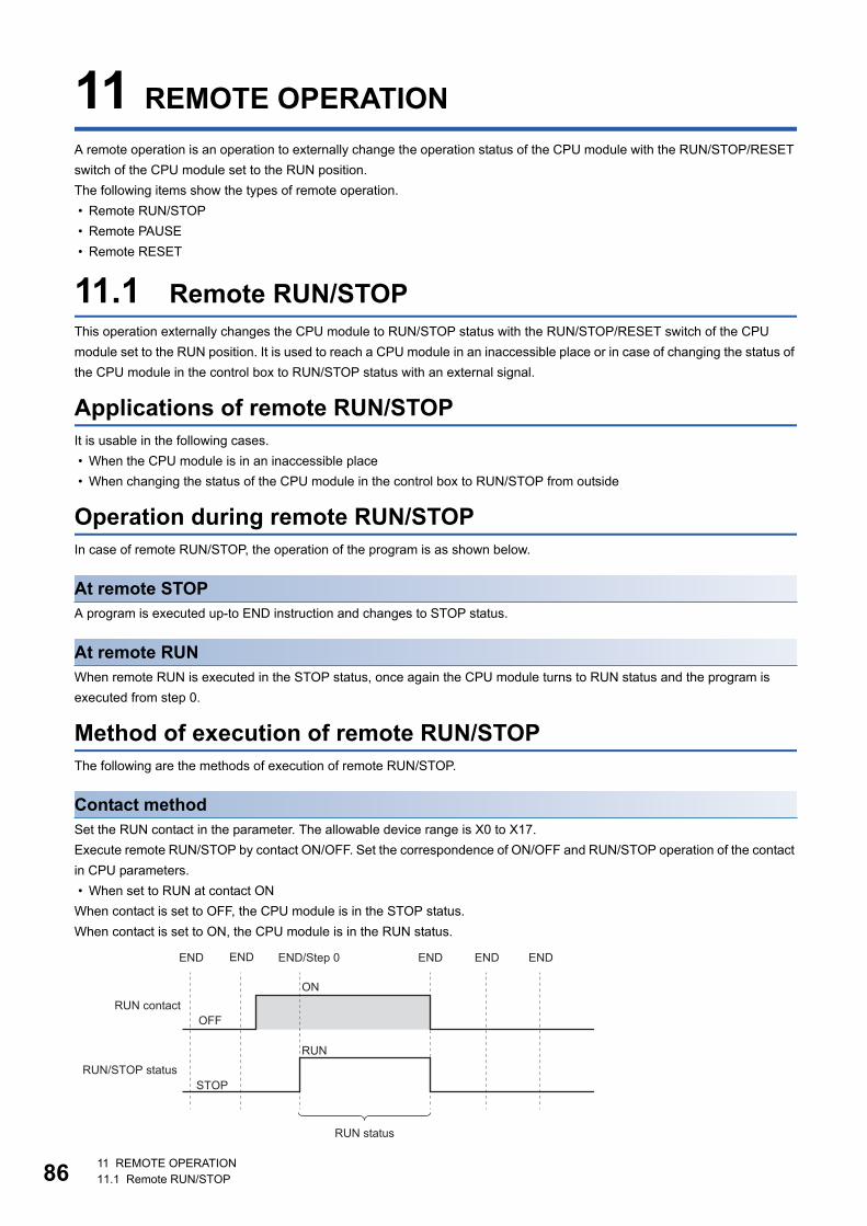
8611 REMOTE OPERATION
11.1 Remote RUN/STOP
11 REMOTE OPERATION
A remote operation is an operation to externally change the operation status of the CPU module with the RUN/STOP/RESET
switch of the CPU module set to the RUN position.
The following items show the types of remote operation.
� Remote RUN/STOP
� Remote PAUSE
� Remote RESET
11.1 Remote RUN/STOP
This operation externally changes the CPU module to RUN/STOP status with the RUN/STOP/RESET switch of the CPU
module set to the RUN position. It is used to reach a CPU module in an inaccessible place or in case of changing the status of
the CPU module in the control box to RUN/STOP status with an external signal.
Applications of remote RUN/STOP
It is usable in the following cases.
� When the CPU module is in an inaccessible place
� When changing the status of the CPU module in the control box to RUN/STOP from outside
Operation during remote RUN/STOP
In case of remote RUN/STOP, the operation of the program is as shown below.
At remote STOP
A program is executed up-to END instruction and changes to STOP status.
At remote RUN
When remote RUN is executed in the STOP status, once again the CPU module turns to RUN status and the program is
executed from step 0.
Method of execution of remote RUN/STOP
The following are the methods of execution of remote RUN/STOP.
Contact method
Set the RUN contact in the parameter. The allowable device range is X0 to X17.
Execute remote RUN/STOP by contact ON/OFF. Set the correspondence of ON/OFF and RUN/STOP operation of the contact
in CPU parameters.
� When set to RUN at contact ON
When contact is set to OFF, the CPU module is in the STOP status.
When contact is set to ON, the CPU module is in the RUN status.
END ENDEND END/Step 0
ON
OFF
RUN
STOP
RUN status
RUN contact
RUN/STOP status
END END
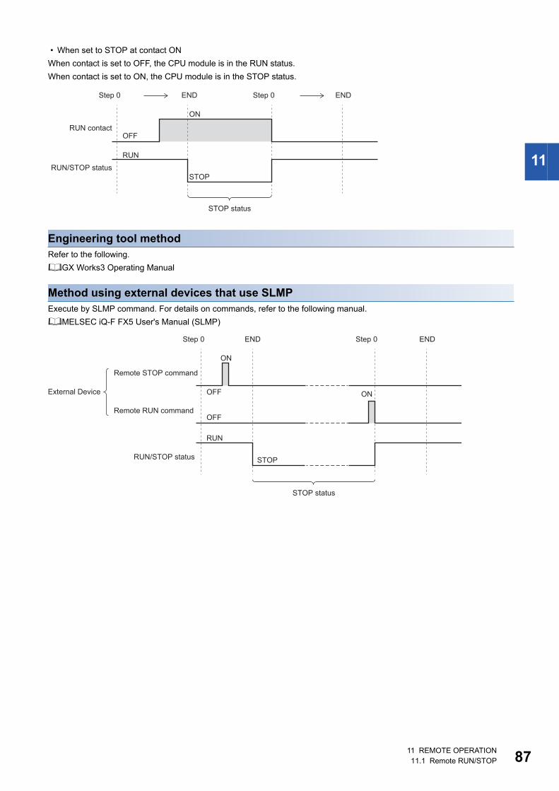
11 REMOTE OPERATION
11.1 Remote RUN/STOP 87
11
� When set to STOP at contact ON
When contact is set to OFF, the CPU module is in the RUN status.
When contact is set to ON, the CPU module is in the STOP status.
Engineering tool method
Refer to the following.
GX Works3 Operating Manual
Method using external devices that use SLMP
Execute by SLMP command. For details on commands, refer to the following manual.
MELSEC iQ-F FX5 User's Manual (SLMP)
Step 0 ENDStep 0 END
ON
OFF
STOP
RUN
STOP status
RUN contact
RUN/STOP status
RUN
OFF
Step 0 ENDStep 0 END
ON
ONOFF
STOP
STOP status
Remote RUN command
Remote STOP command
RUN/STOP status
External Device
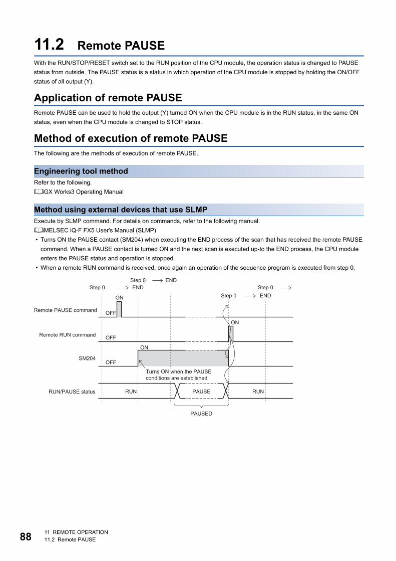
8811 REMOTE OPERATION
11.2 Remote PAUSE
11.2 Remote PAUSE
With the RUN/STOP/RESET switch set to the RUN position of the CPU module, the operation status is changed to PAUSE
status from outside. The PAUSE status is a status in which operation of the CPU module is stopped by holding the ON/OFF
status of all output (Y).
Application of remote PAUSE
Remote PAUSE can be used to hold the output (Y) turned ON when the CPU module is in the RUN status, in the same ON
status, even when the CPU module is changed to STOP status.
Method of execution of remote PAUSE
The following are the methods of execution of remote PAUSE.
Engineering tool method
Refer to the following.
GX Works3 Operating Manual
Method using external devices that use SLMP
Execute by SLMP command. For details on commands, refer to the following manual.
MELSEC iQ-F FX5 User's Manual (SLMP)
� Turns ON the PAUSE contact (SM204) when executing the END process of the scan that has received the remote PAUSE
command. When a PAUSE contact is turned ON and the next scan is executed up-to the END process, the CPU module
enters the PAUSE status and operation is stopped.
� When a remote RUN command is received, once again an operation of the sequence program is executed from step 0.
RUNPAUSERUN
OFF
OFF
Step 0
Step 0 END
Step 0 END
Step 0 END
ON
ON
ON
OFF
PAUSED
Remote RUN command
Remote PAUSE command
RUN/PAUSE status
SM204
Turns ON when the PAUSE
conditions are established
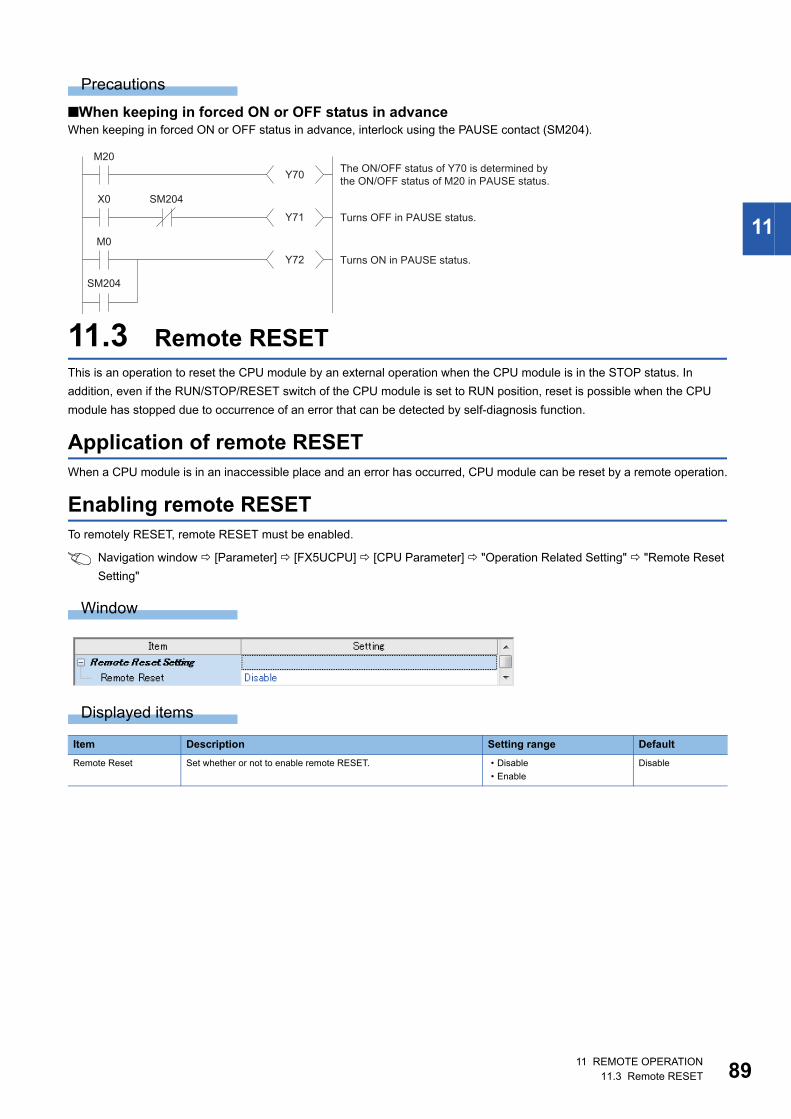
11 REMOTE OPERATION
11.3 Remote RESET 89
11
Precautions
■When keeping in forced ON or OFF status in advanceWhen keeping in forced ON or OFF status in advance, interlock using the PAUSE contact (SM204).
11.3 Remote RESET
This is an operation to reset the CPU module by an external operation when the CPU module is in the STOP status. In
addition, even if the RUN/STOP/RESET switch of the CPU module is set to RUN position, reset is possible when the CPU
module has stopped due to occurrence of an error that can be detected by self-diagnosis function.
Application of remote RESET
When a CPU module is in an inaccessible place and an error has occurred, CPU module can be reset by a remote operation.
Enabling remote RESET
To remotely RESET, remote RESET must be enabled.
Navigation window [Parameter] [FX5UCPU] [CPU Parameter] "Operation Related Setting" "Remote Reset
Setting"
Window
Displayed items
Item Description Setting range Default
Remote Reset Set whether or not to enable remote RESET. � Disable
� Enable
Disable
SM204
M0
Y72 Turns ON in PAUSE status.
SM204X0
Y71 Turns OFF in PAUSE status.
M20
Y70The ON/OFF status of Y70 is determined by
the ON/OFF status of M20 in PAUSE status.
9011 REMOTE OPERATION
11.3 Remote RESET
Method of execution of remote RESET
The following are the methods of execution of remote RESET.
Engineering tool method
Refer to the following.
GX Works3 Operating Manual
Method using external devices that use SLMP
Refer to the following.
MELSEC iQ-F FX5 User's Manual (SLMP)
When executing remote RESET, the settings that allow the remote reset of the CPU parameter must be
written to CPU module beforehand. In the case that they are not set, remote RESET will not be possible.
Precautions
■Remote RESET in RUN statusWhen the CPU module is in RUN status, it cannot be reset by remote RESET. Change the CPU module to STOP status by
operations like remote STOP and then execute remote RESET.
■State after completion of the reset processWhen the reset process is completed on a CPU module on which remote RESET was executed, the CPU module will change
to an operation status set by the RUN/STOP/RESET switch. Setting the RUN/STOP/RESET switch to the STOP position, will
change the status to STOP and setting the switch to the RUN position will change the status to RUN.
� Note that if a remote RESET is executed when the CPU module has stopped due to an error, the CPU
module will change to an operation status set by the RUN/STOP/RESET switch, by reset process
completion.
� If status of CPU module does not change even after executing remote RESET by engineering tool, check
the remote reset settings in the CPU parameter. If it is not set, even after completion of the remote process
of engineering tool, reset process of the CPU module will not be carried out.
■When an error occurs due to noiseWhen there an error due to noise, exercise caution as there is a possibility that PLC cannot be reset by remote RESET. When
reset by remote RESET is not possible, either execute reset by RUN/STOP/RESET switch or once again start up the power of
CPU module.
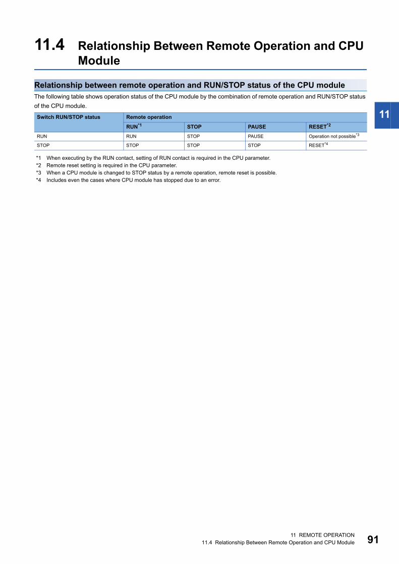
11 REMOTE OPERATION
11.4 Relationship Between Remote Operation and CPU Module 91
11
11.4 Relationship Between Remote Operation and CPU Module
Relationship between remote operation and RUN/STOP status of the CPU module
The following table shows operation status of the CPU module by the combination of remote operation and RUN/STOP status
of the CPU module.
*1 When executing by the RUN contact, setting of RUN contact is required in the CPU parameter.
*2 Remote reset setting is required in the CPU parameter.
*3 When a CPU module is changed to STOP status by a remote operation, remote reset is possible.
*4 Includes even the cases where CPU module has stopped due to an error.
Switch RUN/STOP status Remote operation
RUN*1 STOP PAUSE RESET*2
RUN RUN STOP PAUSE Operation not possible*3
STOP STOP STOP STOP RESET*4
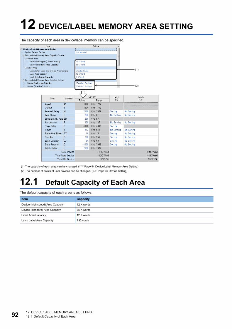
9212 DEVICE/LABEL MEMORY AREA SETTING
12.1 Default Capacity of Each Area
12 DEVICE/LABEL MEMORY AREA SETTING
The capacity of each area in device/label memory can be specified.
12.1 Default Capacity of Each Area
The default capacity of each area is as follows.
(1) The capacity of each area can be changed. (Page 94 Device/Label Memory Area Setting)
(2) The number of points of user devices can be changed. (Page 95 Device Setting)
Item Capacity
Device (high speed) Area Capacity 12 K words
Device (standard) Area Capacity 35 K words
Label Area Capacity 12 K words
Latch Label Area Capacity 1 K words
(1)
(2)
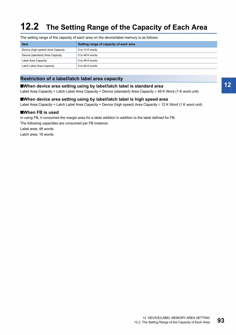
12 DEVICE/LABEL MEMORY AREA SETTING
12.2 The Setting Range of the Capacity of Each Area 93
12
12.2 The Setting Range of the Capacity of Each Area
The setting range of the capacity of each area on the device/label memory is as follows.
Restriction of a label/latch label area capacity
■When device area setting using by label/latch label is standard areaLabel Area Capacity + Latch Label Area Capacity + Device (standard) Area Capacity 48 K Word (1 K word unit)
■When device area setting using by label/latch label is high speed areaLabel Area Capacity + Latch Label Area Capacity + Device (high speed) Area Capacity 12 K Word (1 K word unit)
■When FB is usedIn using FB, it consumes the margin area for a label addition in addition to the label defined for FB.
The following capacities are consumed per FB instance.
Label area: 48 words
Latch area: 16 words
Item Setting range of capacity of each area
Device (high speed) Area Capacity 0 to 12 K words
Device (standard) Area Capacity 0 to 48 K words
Label Area Capacity 0 to 48 K words
Latch Label Area Capacity 0 to 48 K words
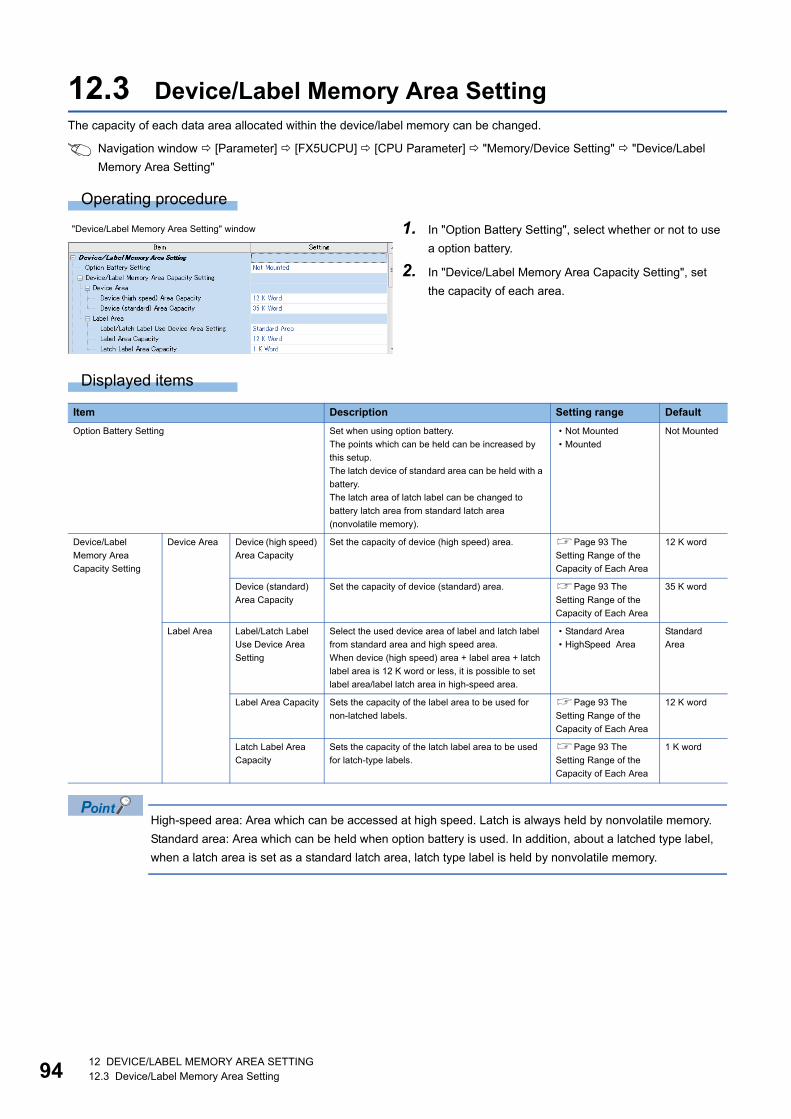
9412 DEVICE/LABEL MEMORY AREA SETTING
12.3 Device/Label Memory Area Setting
12.3 Device/Label Memory Area Setting
The capacity of each data area allocated within the device/label memory can be changed.
Navigation window [Parameter] [FX5UCPU] [CPU Parameter] "Memory/Device Setting" "Device/Label
Memory Area Setting"
Operating procedure
Displayed items
High-speed area: Area which can be accessed at high speed. Latch is always held by nonvolatile memory.
Standard area: Area which can be held when option battery is used. In addition, about a latched type label,
when a latch area is set as a standard latch area, latch type label is held by nonvolatile memory.
"Device/Label Memory Area Setting" window 1. In "Option Battery Setting", select whether or not to use
a option battery.
2. In "Device/Label Memory Area Capacity Setting", set
the capacity of each area.
Item Description Setting range Default
Option Battery Setting Set when using option battery.
The points which can be held can be increased by
this setup.
The latch device of standard area can be held with a
battery.
The latch area of latch label can be changed to
battery latch area from standard latch area
(nonvolatile memory).
� Not Mounted
� Mounted
Not Mounted
Device/Label
Memory Area
Capacity Setting
Device Area Device (high speed)
Area Capacity
Set the capacity of device (high speed) area. Page 93 The
Setting Range of the
Capacity of Each Area
12 K word
Device (standard)
Area Capacity
Set the capacity of device (standard) area. Page 93 The
Setting Range of the
Capacity of Each Area
35 K word
Label Area Label/Latch Label
Use Device Area
Setting
Select the used device area of label and latch label
from standard area and high speed area.
When device (high speed) area + label area + latch
label area is 12 K word or less, it is possible to set
label area/label latch area in high-speed area.
� Standard Area
� HighSpeed Area
Standard
Area
Label Area Capacity Sets the capacity of the label area to be used for
non-latched labels.
Page 93 The
Setting Range of the
Capacity of Each Area
12 K word
Latch Label Area
Capacity
Sets the capacity of the latch label area to be used
for latch-type labels.
Page 93 The
Setting Range of the
Capacity of Each Area
1 K word
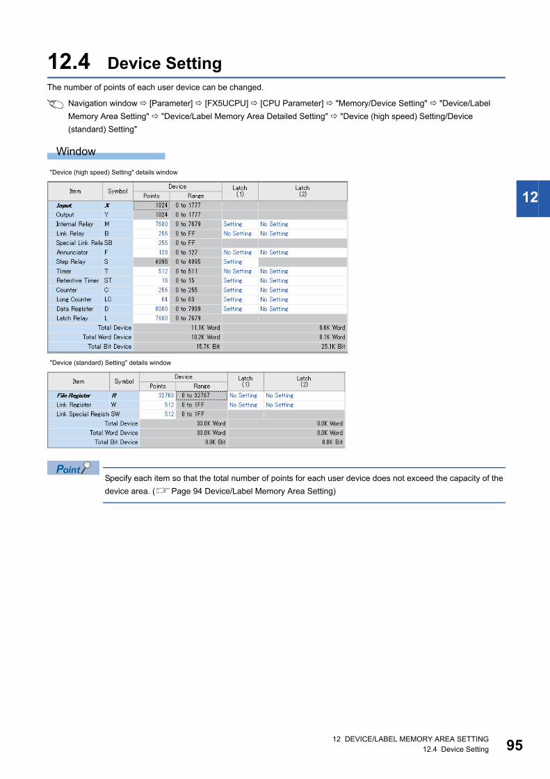
12 DEVICE/LABEL MEMORY AREA SETTING
12.4 Device Setting 95
12
12.4 Device Setting
The number of points of each user device can be changed.
Navigation window [Parameter] [FX5UCPU] [CPU Parameter] "Memory/Device Setting" "Device/Label
Memory Area Setting" "Device/Label Memory Area Detailed Setting" "Device (high speed) Setting/Device
(standard) Setting"
Window
Specify each item so that the total number of points for each user device does not exceed the capacity of the
device area. (Page 94 Device/Label Memory Area Setting)
"Device (high speed) Setting" details window
"Device (standard) Setting" details window
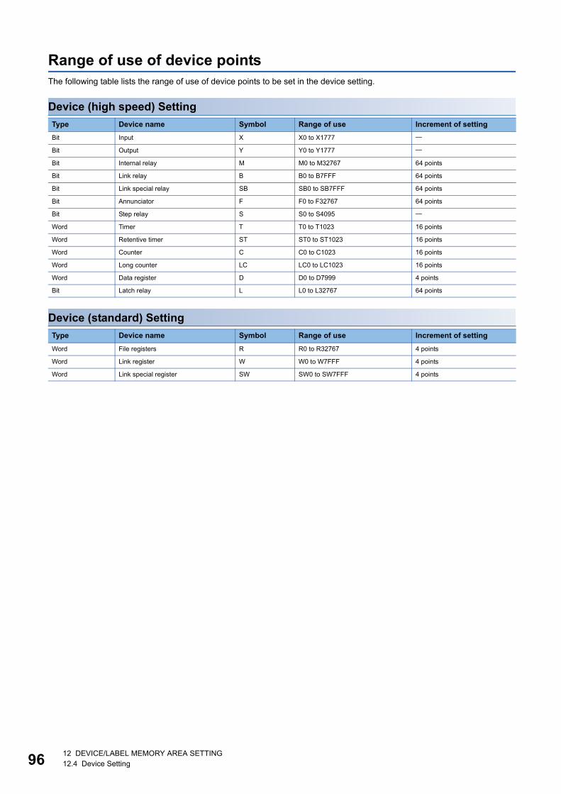
9612 DEVICE/LABEL MEMORY AREA SETTING
12.4 Device Setting
Range of use of device points
The following table lists the range of use of device points to be set in the device setting.
Device (high speed) Setting
Device (standard) Setting
Type Device name Symbol Range of use Increment of setting
Bit Input X X0 to X1777
Bit Output Y Y0 to Y1777
Bit Internal relay M M0 to M32767 64 points
Bit Link relay B B0 to B7FFF 64 points
Bit Link special relay SB SB0 to SB7FFF 64 points
Bit Annunciator F F0 to F32767 64 points
Bit Step relay S S0 to S4095
Word Timer T T0 to T1023 16 points
Word Retentive timer ST ST0 to ST1023 16 points
Word Counter C C0 to C1023 16 points
Word Long counter LC LC0 to LC1023 16 points
Word Data register D D0 to D7999 4 points
Bit Latch relay L L0 to L32767 64 points
Type Device name Symbol Range of use Increment of setting
Word File registers R R0 to R32767 4 points
Word Link register W W0 to W7FFF 4 points
Word Link special register SW SW0 to SW7FFF 4 points
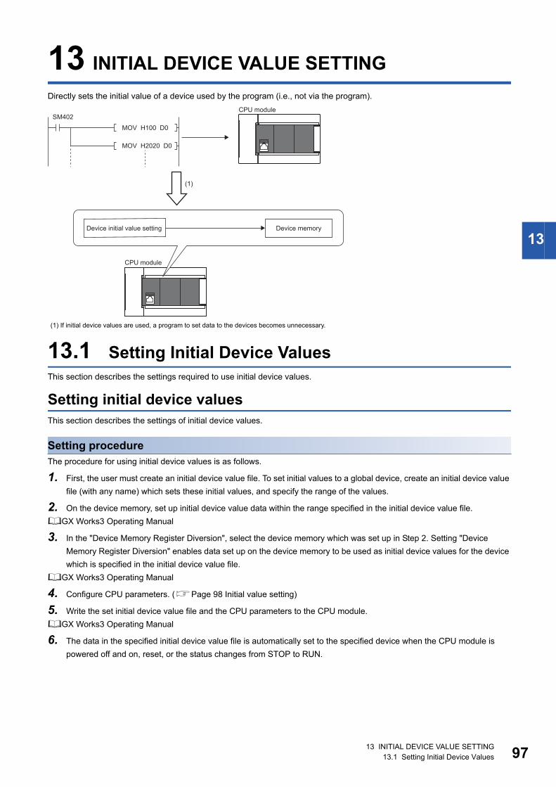
13 INITIAL DEVICE VALUE SETTING
13.1 Setting Initial Device Values 97
13
13 INITIAL DEVICE VALUE SETTING
Directly sets the initial value of a device used by the program (i.e., not via the program).
13.1 Setting Initial Device Values
This section describes the settings required to use initial device values.
Setting initial device values
This section describes the settings of initial device values.
Setting procedure
The procedure for using initial device values is as follows.
1. First, the user must create an initial device value file. To set initial values to a global device, create an initial device value
file (with any name) which sets these initial values, and specify the range of the values.
2. On the device memory, set up initial device value data within the range specified in the initial device value file.
GX Works3 Operating Manual
3. In the "Device Memory Register Diversion", select the device memory which was set up in Step 2. Setting "Device
Memory Register Diversion" enables data set up on the device memory to be used as initial device values for the device
which is specified in the initial device value file.
GX Works3 Operating Manual
4. Configure CPU parameters. (Page 98 Initial value setting)
5. Write the set initial device value file and the CPU parameters to the CPU module.
GX Works3 Operating Manual
6. The data in the specified initial device value file is automatically set to the specified device when the CPU module is
powered off and on, reset, or the status changes from STOP to RUN.
(1) If initial device values are used, a program to set data to the devices becomes unnecessary.
SM402
MOV H100 D0
MOV H2020 D0
(1)
CPU module
CPU module
Device initial value setting Device memory
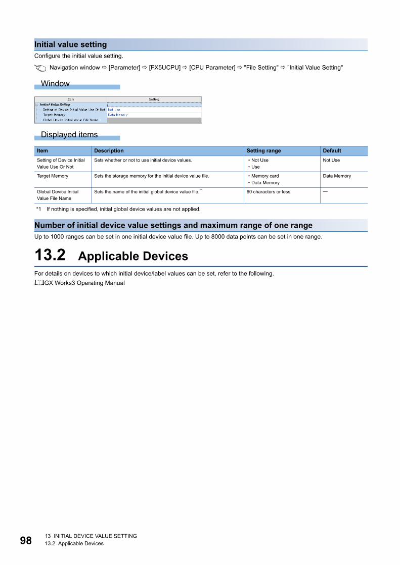
9813 INITIAL DEVICE VALUE SETTING
13.2 Applicable Devices
Initial value setting
Configure the initial value setting.
Navigation window [Parameter] [FX5UCPU] [CPU Parameter] "File Setting" "Initial Value Setting"
Window
Displayed items
*1 If nothing is specified, initial global device values are not applied.
Number of initial device value settings and maximum range of one range
Up to 1000 ranges can be set in one initial device value file. Up to 8000 data points can be set in one range.
13.2 Applicable Devices
For details on devices to which initial device/label values can be set, refer to the following.
GX Works3 Operating Manual
Item Description Setting range Default
Setting of Device Initial
Value Use Or Not
Sets whether or not to use initial device values. � Not Use
� Use
Not Use
Target Memory Sets the storage memory for the initial device value file. � Memory card
� Data Memory
Data Memory
Global Device Initial
Value File Name
Sets the name of the initial global device value file.*1 60 characters or less
14 LATCH FUNCTION
14.1 Types of Latch 99
14
14 LATCH FUNCTION
The contents of each device/label of the CPU module is cleared in the cases described below and changed to its default
value.
� At power OFFON of the CPU module
� At reset
� A power failure that exceeded allowable momentary power interruption
The contents of each device/label with latch setting will be maintained in case of power failure even in the above-mentioned
cases. Therefore, when the data is managed by continuous control, even if power of the CPU is turned OFF or there is a
power failure that exceeds the allowable momentary power interruption, all data can be maintained and control can be
continued.
14.1 Types of Latch
There are two types of latches, latch (1) and latch (2).
Latch clear range can be set by selecting latch (1) or latch (2).
For latch clearing, refer to Page 101 Clearing of Data of the Latch Range.
14.2 Device/label that can be Latched
The devices and labels that can be latched are described below.
The devices that can be latched
The devices that can be latched are described below.
*1 Link register (W) and file register (R) can be latched only when an optional battery is used.
Labels that can be latched
The labels that can be latched are described below.
*1 Only sub-routine type FB can be used.
Device Specification Method Applicable latch type
Internal relay (M) Specify the latch range Latch (1) or Latch (2)
Latch relay (L) Specify the number of points Latch (2) only
Link relay (B) Specify the latch range Latch (1) or Latch (2)
Annunciator (F) Specify the latch range Latch (1) or Latch (2)
Step relay (S) Specify the latch range Latch (1) only
Timer (T)/Accumulation timer (ST) Specify the latch range Latch (1) or Latch (2)
Counter (C)/Long counter (LC) Specify the latch range Latch (1) or Latch (2)
Data register (D) Specify the latch range Latch (1) or Latch (2)
Link register (W)*1 Specify the latch range Latch (1) or Latch (2)
File register (R)*1 Specify the latch range Latch (1) or Latch (2)
Label Type Attribute Data type
Global label VAR_GLOBAL RETAIN Basic data type, array, structure
Local label of the program block VAR
Local label of the Function Block VAR
VAR_INPUT*1
VAR_OUTPUT
VAR_PUBLIC
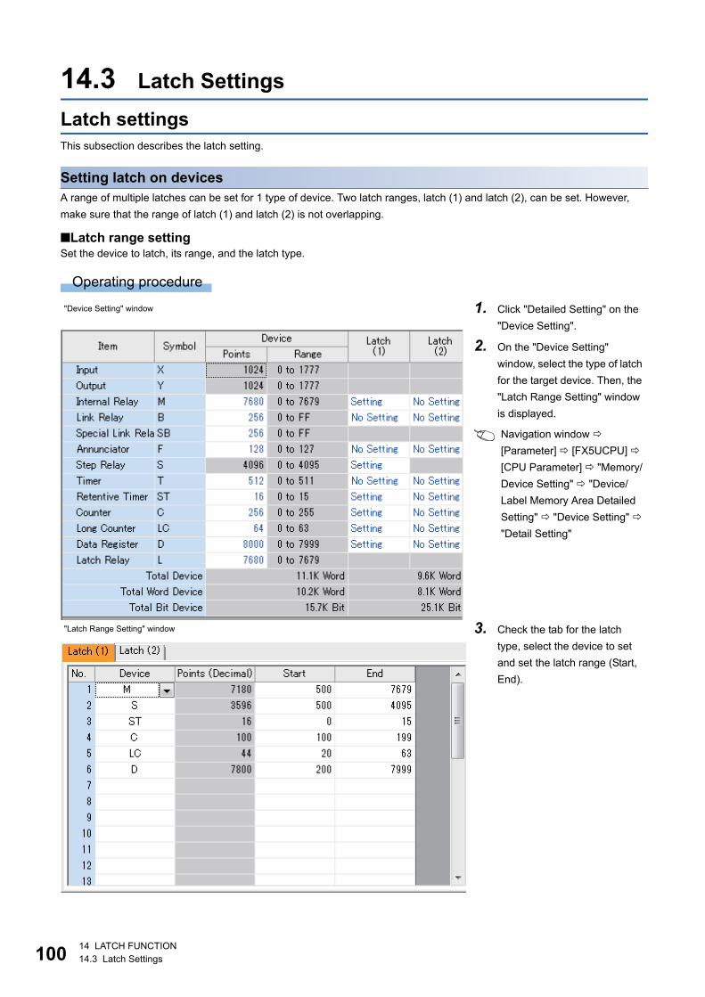
10014 LATCH FUNCTION
14.3 Latch Settings
14.3 Latch Settings
Latch settings
This subsection describes the latch setting.
Setting latch on devices
A range of multiple latches can be set for 1 type of device. Two latch ranges, latch (1) and latch (2), can be set. However,
make sure that the range of latch (1) and latch (2) is not overlapping.
■Latch range settingSet the device to latch, its range, and the latch type.
Operating procedure
"Device Setting" window 1. Click "Detailed Setting" on the
"Device Setting".
2. On the "Device Setting"
window, select the type of latch
for the target device. Then, the
"Latch Range Setting" window
is displayed.
Navigation window
[Parameter] [FX5UCPU]
[CPU Parameter] "Memory/
Device Setting" "Device/
Label Memory Area Detailed
Setting" "Device Setting"
"Detail Setting"
"Latch Range Setting" window 3. Check the tab for the latch
type, select the device to set
and set the latch range (Start,
End).
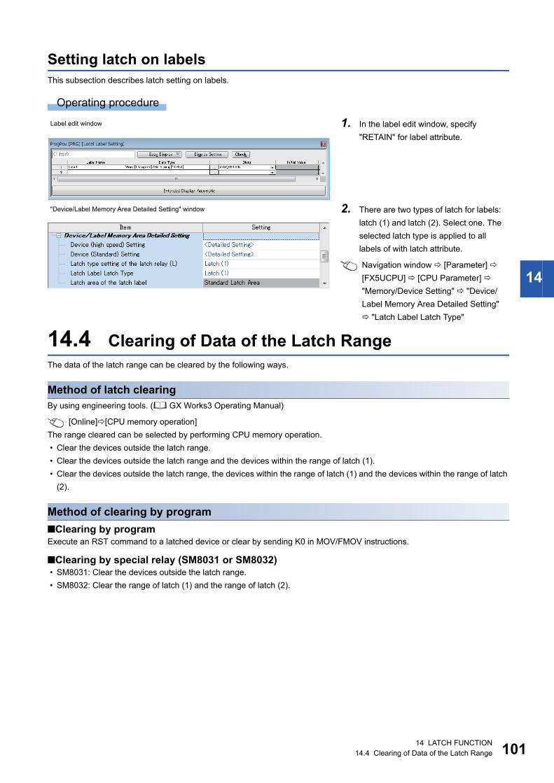
14 LATCH FUNCTION
14.4 Clearing of Data of the Latch Range 101
14
Setting latch on labels
This subsection describes latch setting on labels.
Operating procedure
14.4 Clearing of Data of the Latch Range
The data of the latch range can be cleared by the following ways.
Method of latch clearing
By using engineering tools. ( GX Works3 Operating Manual)
[Online][CPU memory operation]
The range cleared can be selected by performing CPU memory operation.
� Clear the devices outside the latch range.
� Clear the devices outside the latch range and the devices within the range of latch (1).
� Clear the devices outside the latch range, the devices within the range of latch (1) and the devices within the range of latch
(2).
Method of clearing by program
■Clearing by programExecute an RST command to a latched device or clear by sending K0 in MOV/FMOV instructions.
■Clearing by special relay (SM8031 or SM8032) � SM8031: Clear the devices outside the latch range.
� SM8032: Clear the range of latch (1) and the range of latch (2).
Label edit window 1. In the label edit window, specify
"RETAIN" for label attribute.
"Device/Label Memory Area Detailed Setting" window 2. There are two types of latch for labels:
latch (1) and latch (2). Select one. The
selected latch type is applied to all
labels of with latch attribute.
Navigation window [Parameter]
[FX5UCPU] [CPU Parameter]
"Memory/Device Setting" "Device/
Label Memory Area Detailed Setting"
"Latch Label Latch Type"
10214 LATCH FUNCTION
14.5 Precautions
14.5 Precautions
The precaution to be taken when using a latch function is described below.
� When latch range and device no. of points are changed in the parameter, the latching for devices other than link register
(W) and latch label will be the same as the latch settings before the change. Also, if the latch range setting parameter at the
time of previous operation is different from that at the time of the current operation after the CPU module is powered OFF
and ON or reset, the latch data is recovered only in the overlapping part of the latch ranges.
� When latch range and the number of devices are changed in the parameter, all latch labels are cleared to "0".
� When the CPU parameter, program file, FB file, and global label setting file are changed, all latch labels are cleared to "0".
� Special relays and special registers are not cleared even by performing CPU memory operation or special relay clearing.
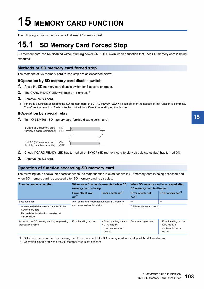
15 MEMORY CARD FUNCTION
15.1 SD Memory Card Forced Stop 103
15
15 MEMORY CARD FUNCTION
The following explains the functions that use SD memory card.
15.1 SD Memory Card Forced Stop
SD memory card can be disabled without turning power ONOFF, even when a function that uses SD memory card is being
executed.
Methods of SD memory card forced stop
The methods of SD memory card forced stop are as described below.
■Operation by SD memory card disable switch
1. Press the SD memory card disable switch for 1 second or longer.
2. The CARD READY LED will flash onturn off.*1
3. Remove the SD card.
*1 If there is a function accessing the SD memory card, the CARD READY LED will flash off after the access of that function is complete.
Therefore, the time from flash on to flash off will be different depending on the function.
■Operation by special relay
1. Turn ON SM606 (SD memory card forcibly disable command).
2. Check if CARD READY LED has turned off or SM607 (SD memory card forcibly disable status flag) has turned ON.
3. Remove the SD card.
Operation of function accessing SD memory card
The following table shows the operation when the main function is executed while SD memory card is being accessed and
when SD memory card is accessed after SD memory card is disabled.
*1 Set whether an error due to accessing the SD memory card after SD memory card forced stop will be detected or not.
*2 Operation is same as when the SD memory card is not attached.
Function under execution When main function is executed while SD
memory card is being
When SD memory card is accessed after
SD memory card is disabled
Error check not
set*1Error check set*1 Error check not
set*1Error check set*1
Boot operation After completing execution function, SD memory
card turns to disabled status.
� Access to the label/device comment in the
SD memory card
� Device/label initialization operation at
STOPRUN
CPU module error occurs.*2
Access to the SD memory card by engineering
tool/SLMP function
Error handling occurs. � Error handling occurs.
� CPU module
continuation error
occurs.
Error handling occurs. � Error handling occurs.
� CPU module
continuation error
occurs.
ONOFF
ONOFF
SM606 (SD memory card
forcibly disable command)
SM607 (SD memory card
forcibly disable status flag)
10415 MEMORY CARD FUNCTION
15.2 Boot Operation
Releasing the SD memory card forced stop status
After the SD memory card has turned to disable status, release the SD memory card forced stop status by the operation
shown below.
1. Load SD card again.*1
2. Turn OFFON the power or reset the CPU module.
*1 The CARD READY LED will blinklight up.
Precautions
The precaution regarding SD memory card forced stop is described below.
� When a forced stop operation is carried out by SD memory card disable switch and forced stop operation by SM606,
operation carried out earlier becomes valid, and the operation that is carried out later becomes invalid. For example, after
the forced stop by SD memory card disable switch, when SM606 is turned ONOFF without removing the SD memory
card, the disable status of the SD memory card can be released. After the forced stop by SD memory card disable switch,
when SD memory card is removed and then SM606 is turned ON, SM606 operation is ignored.
15.2 Boot Operation
At the time of power OFFON or reset of the CPU module, a file which is stored on the SD memory card is transferred to the
memory of the transfer destination which the CPU module judged automatically.
Boot operation procedure
The selectable files for boot operation are listed below.
1. Carry out the boot file settings.
2. Load SD memory card.
3. Write the boot file settings and boot file to the SD memory card.
4. Turn OFFON the power or reset the CPU module.
Specifiable file types
The procedure of boot operation is explained below.
� Parameter files (system parameters, CPU parameters, module parameters, module extension parameters)
� Remote password
� Global labels (global label setting files, initial label values)
� Program files (programs, restored information)
� FB files (FB, restored information)
� Device comments
� Initial device values
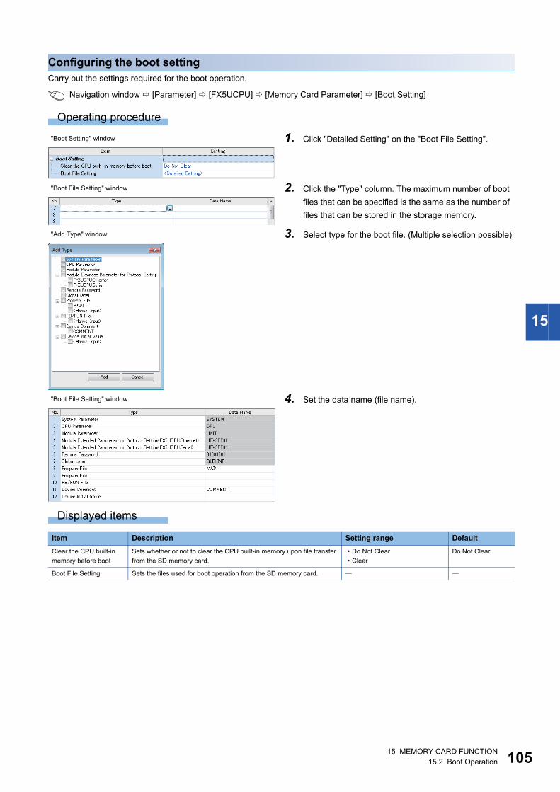
15 MEMORY CARD FUNCTION
15.2 Boot Operation 105
15
Configuring the boot setting
Carry out the settings required for the boot operation.
Navigation window [Parameter] [FX5UCPU] [Memory Card Parameter] [Boot Setting]
Operating procedure
Displayed items
"Boot Setting" window 1. Click "Detailed Setting" on the "Boot File Setting".
"Boot File Setting" window 2. Click the "Type" column. The maximum number of boot
files that can be specified is the same as the number of
files that can be stored in the storage memory.
"Add Type" window 3. Select type for the boot file. (Multiple selection possible)
"Boot File Setting" window 4. Set the data name (file name).
Item Description Setting range Default
Clear the CPU built-in
memory before boot
Sets whether or not to clear the CPU built-in memory upon file transfer
from the SD memory card.
� Do Not Clear
� Clear
Do Not Clear
Boot File Setting Sets the files used for boot operation from the SD memory card.
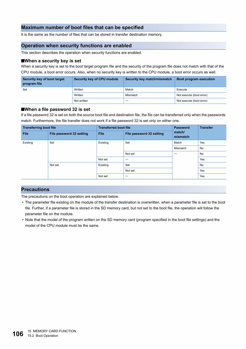
10615 MEMORY CARD FUNCTION
15.2 Boot Operation
Maximum number of boot files that can be specified
It is the same as the number of files that can be stored in transfer destination memory.
Operation when security functions are enabled
This section describes the operation when security functions are enabled.
■When a security key is setWhen a security key is set to the boot target program file and the security of the program file does not match with that of the
CPU module, a boot error occurs. Also, when no security key is written to the CPU module, a boot error occurs as well.
■When a file password 32 is setIf a file password 32 is set on both the source boot file and destination file, the file can be transferred only when the passwords
match. Furthermore, the file transfer does not work if a file password 32 is set only on either one.
Precautions
The precautions on the boot operation are explained below.
� The parameter file existing on the module of the transfer destination is overwritten, when a parameter file is set to the boot
file. Further, if a parameter file is stored in the SD memory card, but not set to the boot file, the operation will follow the
parameter file on the module.
� Note that the model of the program written on the SD memory card (program specified in the boot file settings) and the
model of the CPU module must be the same.
Security key of boot target
program file
Security key of CPU module Security key match/mismatch Boot program execution
Set Written Match Execute
Written Mismatch Not execute (boot error)
Not written Not execute (boot error)
Transferring boot file Transferred boot file Password
match/
mismatch
Transfer
File File password 32 setting File File password 32 setting
Existing Set Existing Set Match Yes
Mismatch No
Not set No
Not set Yes
Not set Existing Set No
Not set Yes
Not set Yes
16 DEVICE/LABEL ACCESS SERVICE PROCESSING SETTING
107
16
16 DEVICE/LABEL ACCESS SERVICE
PROCESSING SETTING
This is a function to optionally designate the frequency of execution of the service process that is carried out by the END
process in the parameter.
Improvement of communication response with peripheral equipment and extension of scan time by the service process can
be controlled by service process setting function. With this, building an optimal service process environment on the system is
possible.
About device/label access service processing
Device/label access service processing is a response process for the request statement from peripheral equipment that
occurs asynchronously with the scan process. (A process of "Interpretation of Request statementInternal processing based
on the requestCreating response statement" for 1 request statement)
The execution timing of the service process is during the END process.
When every request statement from all connected peripheral equipment is executed in each END process,
depending on the number of request statements arriving during 1 scan, the impact on scan time (delay,
scattering) may be big. Therefore, by setting the frequency (number of ports) of device/label access service
processing to be executed in 1 END processing and regulating the frequency of device/label access service
processing according to the system built, ensuring balance between scan time and response time to the
peripheral equipment can be achieved.
Compatibility of service process setting
The compatibility of service process setting is described below.
: Compatible, : Not compatible
Operation details of service process
The operation details of service process are described below.
The following table shows the methods for service process with their respective features.
Communication type Function Compatibility
Serial communication MELSOFT connection
MC protocol communication
MODBUS communication (slave)
N:N Network
MODBUS communication (master)
Non-protocol communication
Inverter communication
Predefined protocol support
Ethernet communication MELSOFT connection
SLMP communication
Socket communication
Predefined protocol support
Device/label access service
processing setting
Scan performance Service process
performance
Device
splitting*5
Features
Extension*1
Stability*2
Response
time*3Stability*4
None Large Medium Fast High None Effective when service process is given
precedence.
Set the frequency of service process Medium High Medium Medium None Effective when scan process is given precedence.
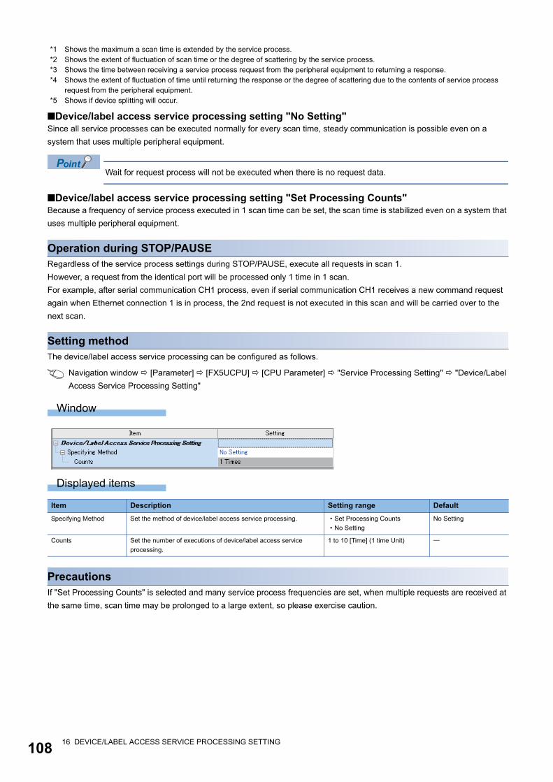
10816 DEVICE/LABEL ACCESS SERVICE PROCESSING SETTING
*1 Shows the maximum a scan time is extended by the service process.
*2 Shows the extent of fluctuation of scan time or the degree of scattering by the service process.
*3 Shows the time between receiving a service process request from the peripheral equipment to returning a response.
*4 Shows the extent of fluctuation of time until returning the response or the degree of scattering due to the contents of service process
request from the peripheral equipment.
*5 Shows if device splitting will occur.
■Device/label access service processing setting "No Setting"Since all service processes can be executed normally for every scan time, steady communication is possible even on a
system that uses multiple peripheral equipment.
Wait for request process will not be executed when there is no request data.
■Device/label access service processing setting "Set Processing Counts"Because a frequency of service process executed in 1 scan time can be set, the scan time is stabilized even on a system that
uses multiple peripheral equipment.
Operation during STOP/PAUSE
Regardless of the service process settings during STOP/PAUSE, execute all requests in scan 1.
However, a request from the identical port will be processed only 1 time in 1 scan.
For example, after serial communication CH1 process, even if serial communication CH1 receives a new command request
again when Ethernet connection 1 is in process, the 2nd request is not executed in this scan and will be carried over to the
next scan.
Setting method
The device/label access service processing can be configured as follows.
Navigation window [Parameter] [FX5UCPU] [CPU Parameter] "Service Processing Setting" "Device/Label
Access Service Processing Setting"
Window
Displayed items
Precautions
If "Set Processing Counts" is selected and many service process frequencies are set, when multiple requests are received at
the same time, scan time may be prolonged to a large extent, so please exercise caution.
Item Description Setting range Default
Specifying Method Set the method of device/label access service processing. � Set Processing Counts
� No Setting
No Setting
Counts Set the number of executions of device/label access service
processing.
1 to 10 [Time] (1 time Unit)
17 RAS FUNCTIONS
17.1 Self-Diagnostics Function 109
1717 RAS FUNCTIONS
17.1 Self-Diagnostics Function
Checks if a problem exists with the CPU module.
Self-diagnostics timing
If an error occurs when the CPU module is powered on or while it is in the RUN/STOP state, the CPU module detects, and
displays it, and stops operation. However, depending on the error occurrence status or the instruction to execute, the CPU
module may not be able to detect the error. Configure safety circuits external to the programmable controller to ensure that
the entire system operates safely even in such a case.
Check method of error
This section describes the check methods when error occurs.
Check method using special relay and special register
When the CPU module detects an error, it turns SM0 (Latest Self-diagnostics error (annunciator on included)) and SM1
(Latest Self-diagnostics error (annunciator on not included)) on and stores the error code corresponding to the error definition
in SD0 (diagnostics error). If multiple errors are detected, the latest error code is stored in SD0. Use SM0, SM1, and SD0 on
the program for the CPU module or mechanical interlock. Besides, the error code up to 16 pieces for the error contents being
currently generated will be stored into SD10 (Self-diagnostics error code) to SD25 (Self-diagnostics error code). (The error
code for the error content of 17th piece on and after will not be stored.)
Check method using LED
The error occurrence conditions can be checked through the lighting conditions of ERR LED. (MELSEC iQ-F FX5U User's
Manual (Hardware), MELSEC iQ-F FX5UC User's Manual (Hardware))
Check method using the engineering tool
The error being currently generated can be checked in the Module diagnostics window. (GX Works3 Operating Manual)
■Existing errorsUp to 16 errors (description of errors) currently existing in the CPU module can be displayed. However, even when an
additional error occurs after a stop error, the error information is not refreshed.
The maximum number of displayable errors is 15 for continuation errors and 1 for stop errors. When 15
continuation errors are displayed and another one occurs, description of the new error is not displayed. Also,
when an error with the same code has already been displayed, the date and time of occurrence and detailed
information of the relevant error are not updated.
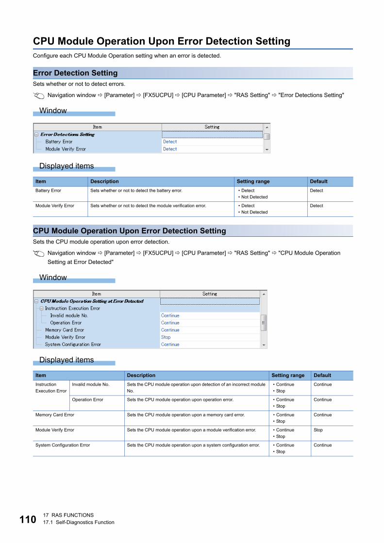
11017 RAS FUNCTIONS
17.1 Self-Diagnostics Function
CPU Module Operation Upon Error Detection Setting
Configure each CPU Module Operation setting when an error is detected.
Error Detection Setting
Sets whether or not to detect errors.
Navigation window [Parameter] [FX5UCPU] [CPU Parameter] "RAS Setting" "Error Detections Setting"
Window
Displayed items
CPU Module Operation Upon Error Detection Setting
Sets the CPU module operation upon error detection.
Navigation window [Parameter] [FX5UCPU] [CPU Parameter] "RAS Setting" "CPU Module Operation
Setting at Error Detected"
Window
Displayed items
Item Description Setting range Default
Battery Error Sets whether or not to detect the battery error. � Detect
� Not Detected
Detect
Module Verify Error Sets whether or not to detect the module verification error. � Detect
� Not Detected
Detect
Item Description Setting range Default
Instruction
Execution Error
Invalid module No. Sets the CPU module operation upon detection of an incorrect module
No.
� Continue
� Stop
Continue
Operation Error Sets the CPU module operation upon operation error. � Continue
� Stop
Continue
Memory Card Error Sets the CPU module operation upon a memory card error. � Continue
� Stop
Continue
Module Verify Error Sets the CPU module operation upon a module verification error. � Continue
� Stop
Stop
System Configuration Error Sets the CPU module operation upon a system configuration error. � Continue
� Stop
Continue
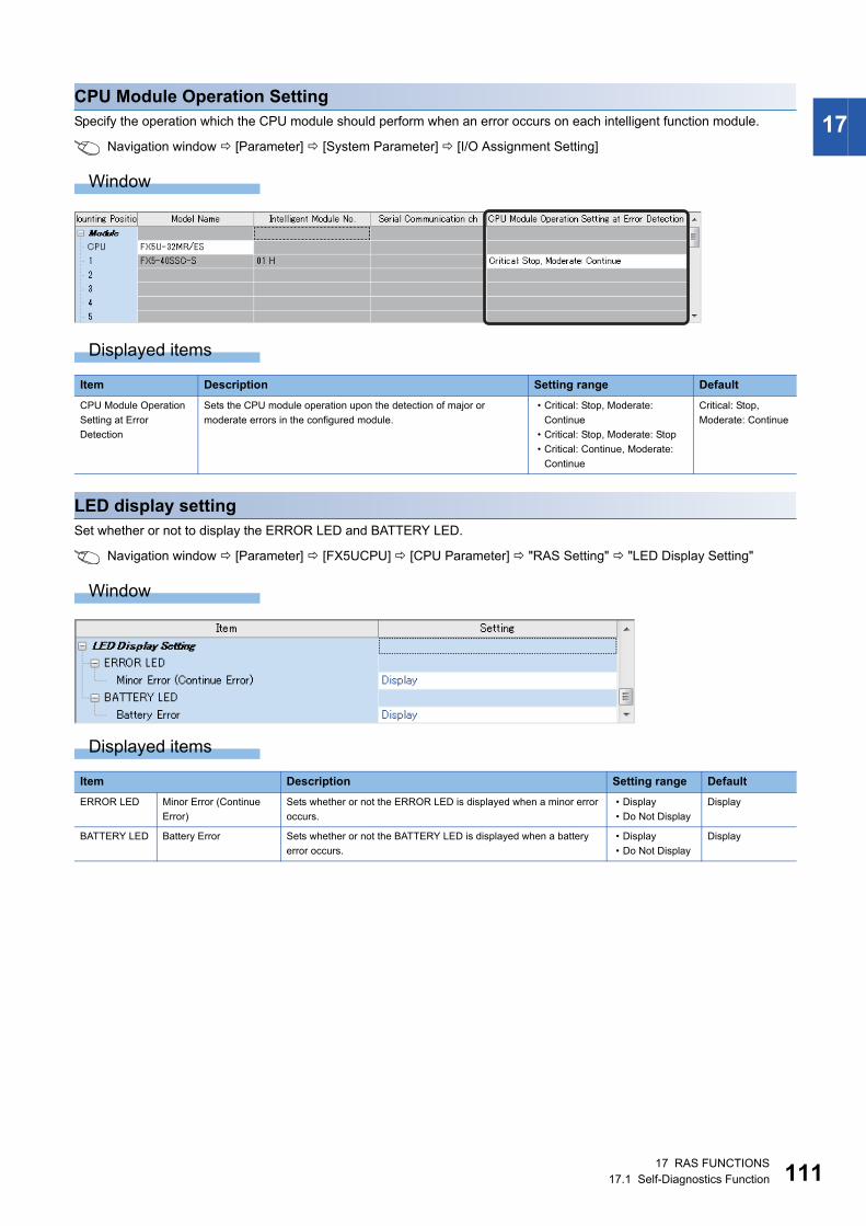
17 RAS FUNCTIONS
17.1 Self-Diagnostics Function 111
17
CPU Module Operation Setting
Specify the operation which the CPU module should perform when an error occurs on each intelligent function module.
Navigation window [Parameter] [System Parameter] [I/O Assignment Setting]
Window
Displayed items
LED display setting
Set whether or not to display the ERROR LED and BATTERY LED.
Navigation window [Parameter] [FX5UCPU] [CPU Parameter] "RAS Setting" "LED Display Setting"
Window
Displayed items
Item Description Setting range Default
CPU Module Operation
Setting at Error
Detection
Sets the CPU module operation upon the detection of major or
moderate errors in the configured module.
� Critical: Stop, Moderate:
Continue
� Critical: Stop, Moderate: Stop
� Critical: Continue, Moderate:
Continue
Critical: Stop,
Moderate: Continue
Item Description Setting range Default
ERROR LED Minor Error (Continue
Error)
Sets whether or not the ERROR LED is displayed when a minor error
occurs.
� Display
� Do Not Display
Display
BATTERY LED Battery Error Sets whether or not the BATTERY LED is displayed when a battery
error occurs.
� Display
� Do Not Display
Display
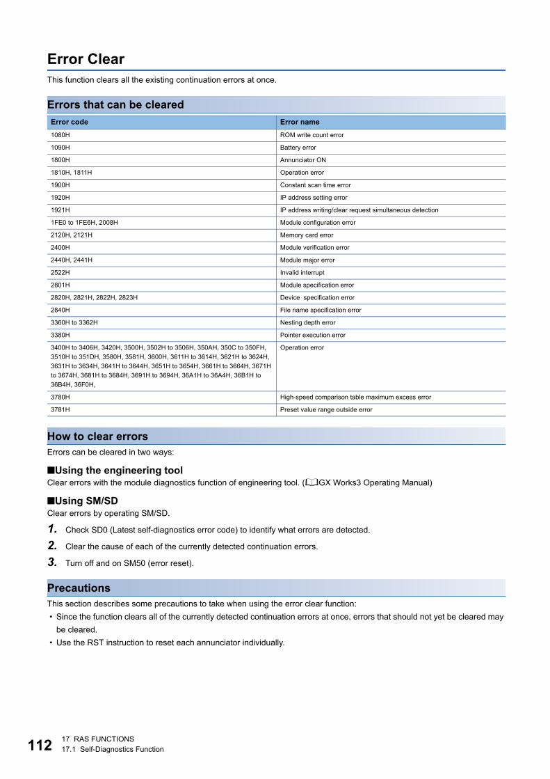
11217 RAS FUNCTIONS
17.1 Self-Diagnostics Function
Error Clear
This function clears all the existing continuation errors at once.
Errors that can be cleared
How to clear errors
Errors can be cleared in two ways:
■Using the engineering toolClear errors with the module diagnostics function of engineering tool. (GX Works3 Operating Manual)
■Using SM/SDClear errors by operating SM/SD.
1. Check SD0 (Latest self-diagnostics error code) to identify what errors are detected.
2. Clear the cause of each of the currently detected continuation errors.
3. Turn off and on SM50 (error reset).
Precautions
This section describes some precautions to take when using the error clear function:
� Since the function clears all of the currently detected continuation errors at once, errors that should not yet be cleared may
be cleared.
� Use the RST instruction to reset each annunciator individually.
Error code Error name
1080H ROM write count error
1090H Battery error
1800H Annunciator ON
1810H, 1811H Operation error
1900H Constant scan time error
1920H IP address setting error
1921H IP address writing/clear request simultaneous detection
1FE0 to 1FE6H, 2008H Module configuration error
2120H, 2121H Memory card error
2400H Module verification error
2440H, 2441H Module major error
2522H Invalid interrupt
2801H Module specification error
2820H, 2821H, 2822H, 2823H Device specification error
2840H File name specification error
3360H to 3362H Nesting depth error
3380H Pointer execution error
3400H to 3406H, 3420H, 3500H, 3502H to 3506H, 350AH, 350C to 350FH,
3510H to 351DH, 3580H, 3581H, 3600H, 3611H to 3614H, 3621H to 3624H,
3631H to 3634H, 3641H to 3644H, 3651H to 3654H, 3661H to 3664H, 3671H
to 3674H, 3681H to 3684H, 3691H to 3694H, 36A1H to 36A4H, 36B1H to
36B4H, 36F0H,
Operation error
3780H High-speed comparison table maximum excess error
3781H Preset value range outside error
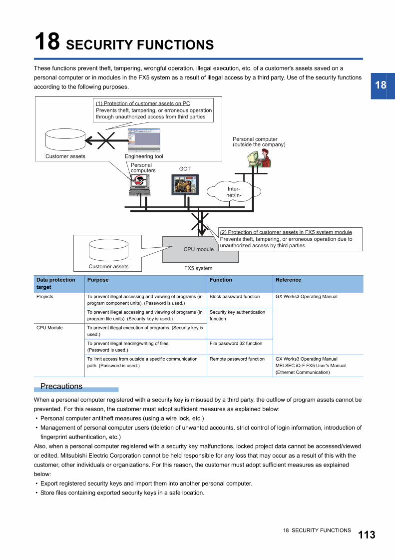
18 SECURITY FUNCTIONS
113
18
18 SECURITY FUNCTIONS
These functions prevent theft, tampering, wrongful operation, illegal execution, etc. of a customer's assets saved on a
personal computer or in modules in the FX5 system as a result of illegal access by a third party. Use of the security functions
according to the following purposes.
Precautions
When a personal computer registered with a security key is misused by a third party, the outflow of program assets cannot be
prevented. For this reason, the customer must adopt sufficient measures as explained below:
� Personal computer antitheft measures (using a wire lock, etc.)
� Management of personal computer users (deletion of unwanted accounts, strict control of login information, introduction of
fingerprint authentication, etc.)
Also, when a personal computer registered with a security key malfunctions, locked project data cannot be accessed/viewed
or edited. Mitsubishi Electric Corporation cannot be held responsible for any loss that may occur as a result of this with the
customer, other individuals or organizations. For this reason, the customer must adopt sufficient measures as explained
below:
� Export registered security keys and import them into another personal computer.
� Store files containing exported security keys in a safe location.
Data protection
target
Purpose Function Reference
Projects To prevent illegal accessing and viewing of programs (in
program component units). (Password is used.)
Block password function GX Works3 Operating Manual
To prevent illegal accessing and viewing of programs (in
program file units). (Security key is used.)
Security key authentication
function
CPU Module To prevent illegal execution of programs. (Security key is
used.)
To prevent illegal reading/writing of files.
(Password is used.)
File password 32 function
To limit access from outside a specific communication
path. (Password is used.)
Remote password function GX Works3 Operating Manual
MELSEC iQ-F FX5 User's Manual
(Ethernet Communication)
Customer assets
Customer assets FX5 system
Engineering tool
GOT
(1) Protection of customer assets on PC
Prevents theft, tampering, or erroneous operation
through unauthorized access from third parties
(2) Protection of customer assets in FX5 system module
Prevents theft, tampering, or erroneous operation due to
unauthorized access by third partiesCPU module
Inter-
net/In-
Personal computers
Personal computer (outside the company)
11419 BUILT-IN I/O FUNCTION
19.1 High-speed Counter Function
19 BUILT-IN I/O FUNCTION
The built-in input/output (I/O) function of the CPU module is explained below.
Each respective function is set by parameters in GX Works3.
19.1 High-speed Counter Function
High-speed counter function is explained below.
High-speed counter function overview
The high-speed counter is a function that counts the number of high-speed pulse inputs that cannot be counted by a
conventional counter, using the general purpose input terminal of the CPU module.
The high-speed counter assigns input and function settings by parameters and operates using the HIOEN instruction.
Parameter setting and the HIOEN instruction are always required to use the high-speed counter.
High-speed counter parameter setting
High-speed counter channels (input allocation, function) and high-speed counter comparison table, etc., are set by
parameters. (Page 123 High-speed counter parameters)
High-speed counter operation mode
The three high-speed counter operation modes are as follows.
Operation mode is set by parameter. (Page 123 High-speed counter parameters)
■Normal modeSelect normal mode if you want to use as an ordinary high-speed counter. (Page 124 High-speed counter (normal mode))
■Pulse density measurement modeSelect pulse density measurement mode if you want to count the number of pulses for a specified amount of time. (Page
126 High-speed counter (pulse density measurement mode))
■Rotational speed measurement modeSelect rotational speed measurement mode if you want to measure speed for a specified amount of time. (Page 129
High-speed counter (rotational speed measurement mode))
High-speed counter dedicated instructions
The high-speed counter starts and stops counting using the HIOEN instruction for the high-speed counter. (MELSEC iQ-F
FX5 Programming Manual (Instructions, Standard Functions/Function Blocks))
Function Reference
High-speed counter function Normal mode Page 124
Pulse density measurement mode Page 126
Rotational speed measurement mode Page 129
FX3-compatible high-speed counter function Page 165
Pulse width measurement function Page 174
Pulse catch function Pulse catch function Page 184
FX3-compatible pulse catch function Page 188
General-purpose input functions Page 191
PWM function Page 193
Built-in positioning function MELSEC iQ-F FX5 User's Manual (Positioning Control)
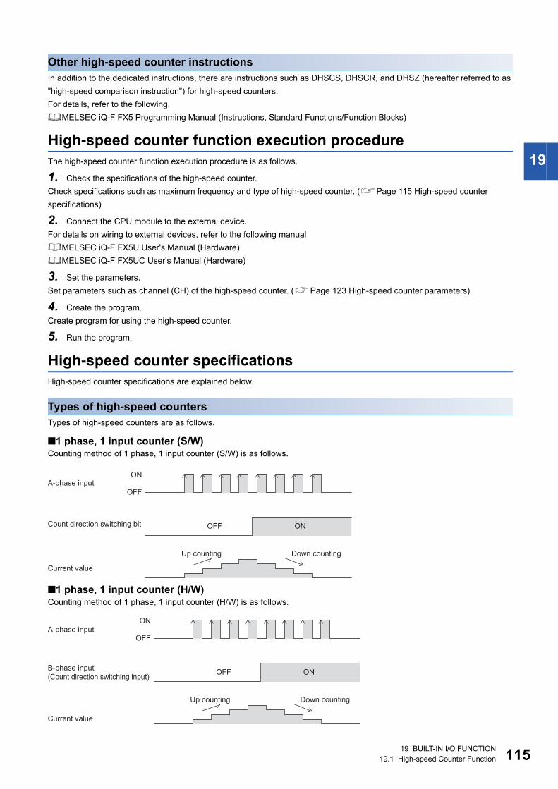
19 BUILT-IN I/O FUNCTION
19.1 High-speed Counter Function 115
19
Other high-speed counter instructions
In addition to the dedicated instructions, there are instructions such as DHSCS, DHSCR, and DHSZ (hereafter referred to as
"high-speed comparison instruction") for high-speed counters.
For details, refer to the following.
MELSEC iQ-F FX5 Programming Manual (Instructions, Standard Functions/Function Blocks)
High-speed counter function execution procedure
The high-speed counter function execution procedure is as follows.
1. Check the specifications of the high-speed counter.
Check specifications such as maximum frequency and type of high-speed counter. (Page 115 High-speed counter
specifications)
2. Connect the CPU module to the external device.
For details on wiring to external devices, refer to the following manual
MELSEC iQ-F FX5U User's Manual (Hardware)
MELSEC iQ-F FX5UC User's Manual (Hardware)
3. Set the parameters.
Set parameters such as channel (CH) of the high-speed counter. (Page 123 High-speed counter parameters)
4. Create the program.
Create program for using the high-speed counter.
5. Run the program.
High-speed counter specifications
High-speed counter specifications are explained below.
Types of high-speed counters
Types of high-speed counters are as follows.
■1 phase, 1 input counter (S/W)Counting method of 1 phase, 1 input counter (S/W) is as follows.
■1 phase, 1 input counter (H/W)Counting method of 1 phase, 1 input counter (H/W) is as follows.
ON
OFF
Current value
Up counting Down counting
A-phase input
ONOFFCount direction switching bit
ON
OFF
Current value
Up counting Down counting
A-phase input
ONOFFB-phase input
(Count direction switching input)
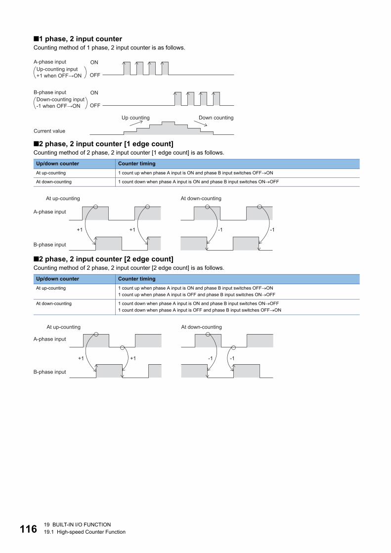
11619 BUILT-IN I/O FUNCTION
19.1 High-speed Counter Function
■1 phase, 2 input counterCounting method of 1 phase, 2 input counter is as follows.
■2 phase, 2 input counter [1 edge count]Counting method of 2 phase, 2 input counter [1 edge count] is as follows.
■2 phase, 2 input counter [2 edge count]Counting method of 2 phase, 2 input counter [2 edge count] is as follows.
Up/down counter Counter timing
At up-counting 1 count up when phase A input is ON and phase B input switches OFFON
At down-counting 1 count down when phase A input is ON and phase B input switches ONOFF
Up/down counter Counter timing
At up-counting 1 count up when phase A input is ON and phase B input switches OFFON
1 count up when phase A input is OFF and phase B input switches ONOFF
At down-counting 1 count down when phase A input is ON and phase B input switches ONOFF
1 count down when phase A input is OFF and phase B input switches OFFON
ON
OFF-1 when OFF→ON
Down-counting input
ON
OFF+1 when OFF→ON
Up-counting input
A-phase input
B-phase input
Current value
Up counting Down counting
-1+1+1
B-phase input
A-phase input
At down-countingAt up-counting
-1
-1+1+1
B-phase input
A-phase input
-1
At down-countingAt up-counting
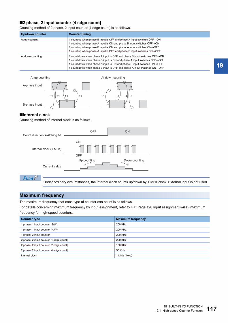
19 BUILT-IN I/O FUNCTION
19.1 High-speed Counter Function 117
19
■2 phase, 2 input counter [4 edge count]Counting method of 2 phase, 2 input counter [4 edge count] is as follows.
■Internal clockCounting method of internal clock is as follows.
Under ordinary circumstances, the internal clock counts up/down by 1 MHz clock. External input is not used.
Maximum frequency
The maximum frequency that each type of counter can count is as follows.
For details concerning maximum frequency by input assignment, refer to Page 120 Input assignment-wise / maximum
frequency for high-speed counters.
Up/down counter Counter timing
At up-counting 1 count up when phase B input is OFF and phase A input switches OFFON
1 count up when phase A input is ON and phase B input switches OFFON
1 count up when phase B input is ON and phase A input switches ONOFF
1 count up when phase A input is OFF and phase B input switches ONOFF
At down-counting 1 count down when phase A input is OFF and phase B input switches OFFON
1 count down when phase B input is ON and phase A input switches OFFON
1 count down when phase A input is ON and phase B input switches ONOFF
1 count down when phase B input is OFF and phase A input switches ONOFF
Counter type Maximum frequency
1 phase, 1 input counter (S/W) 200 KHz
1 phase, 1 input counter (H/W) 200 KHz
1 phase, 2 input counter 200 KHz
2 phase, 2 input counter [1 edge count] 200 KHz
2 phase, 2 input counter [2 edge count] 100 KHz
2 phase, 2 input counter [4 edge count] 50 KHz
Internal clock 1 MHz (fixed)
-1 -1-1+1+1 +1 +1
B-phase input
A-phase input
At down-countingAt up-counting
-1
ON
ON
OFF
OFF
Current value
Up counting Down counting
Internal clock (1 MHz)
Count direction switching bit
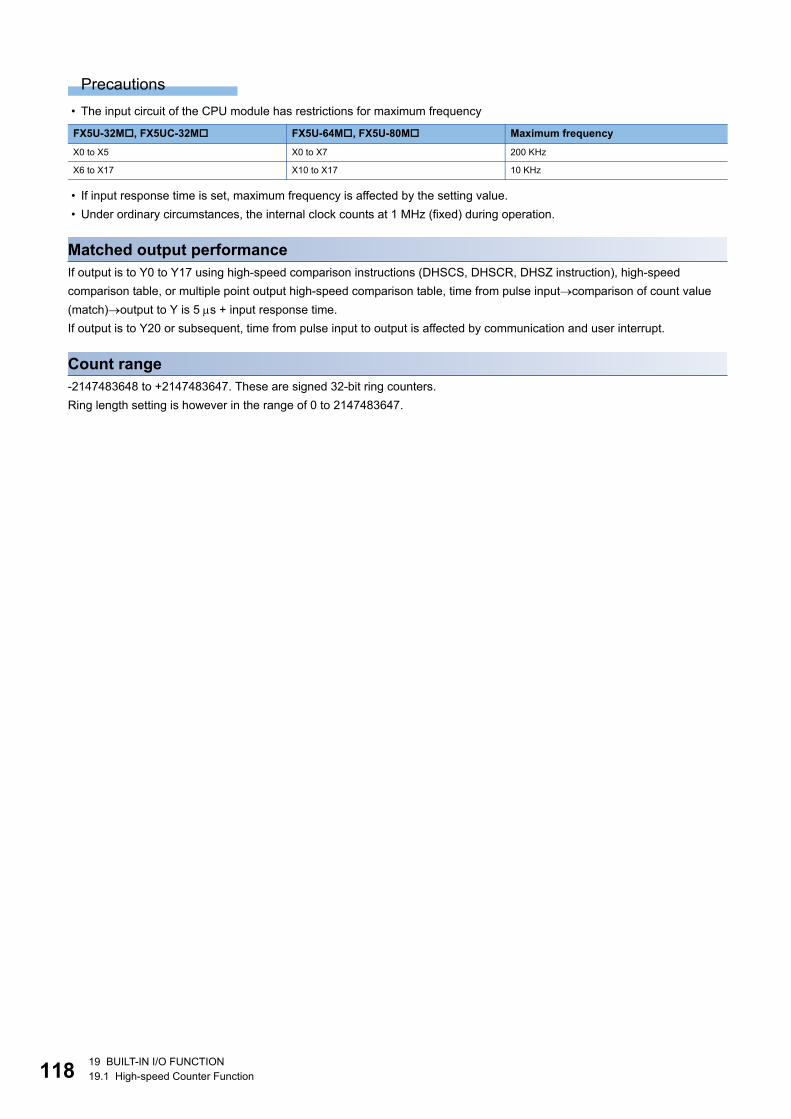
11819 BUILT-IN I/O FUNCTION
19.1 High-speed Counter Function
Precautions
� The input circuit of the CPU module has restrictions for maximum frequency
� If input response time is set, maximum frequency is affected by the setting value.
� Under ordinary circumstances, the internal clock counts at 1 MHz (fixed) during operation.
Matched output performance
If output is to Y0 to Y17 using high-speed comparison instructions (DHSCS, DHSCR, DHSZ instruction), high-speed
comparison table, or multiple point output high-speed comparison table, time from pulse inputcomparison of count value
(match)output to Y is 5 s + input response time.
If output is to Y20 or subsequent, time from pulse input to output is affected by communication and user interrupt.
Count range
-2147483648 to +2147483647. These are signed 32-bit ring counters.
Ring length setting is however in the range of 0 to 2147483647.
FX5U-32M, FX5UC-32M FX5U-64M, FX5U-80M Maximum frequency
X0 to X5 X0 to X7 200 KHz
X6 to X17 X10 to X17 10 KHz
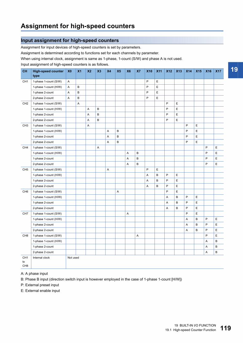
19 BUILT-IN I/O FUNCTION
19.1 High-speed Counter Function 119
19
Assignment for high-speed counters
Input assignment for high-speed counters
Assignment for input devices of high-speed counters is set by parameters.
Assignment is determined according to functions set for each channels by parameter.
When using internal clock, assignment is same as 1-phase, 1-count (S/W) and phase A is not used.
Input assignment of high-speed counters is as follows.
A: A phase input
B: Phase B input (direction switch input is however employed in the case of 1-phase 1-count [H/W])
P: External preset input
E: External enable input
CH High-speed counter
type
X0 X1 X2 X3 X4 X5 X6 X7 X10 X11 X12 X13 X14 X15 X16 X17
CH1 1-phase 1-count (S/W) A P E
1-phase 1-count (H/W) A B P E
1-phase 2-count A B P E
2-phase 2-count A B P E
CH2 1-phase 1-count (S/W) A P E
1-phase 1-count (H/W) A B P E
1-phase 2-count A B P E
2-phase 2-count A B P E
CH3 1-phase 1-count (S/W) A P E
1-phase 1-count (H/W) A B P E
1-phase 2-count A B P E
2-phase 2-count A B P E
CH4 1-phase 1-count (S/W) A P E
1-phase 1-count (H/W) A B P E
1-phase 2-count A B P E
2-phase 2-count A B P E
CH5 1-phase 1-count (S/W) A P E
1-phase 1-count (H/W) A B P E
1-phase 2-count A B P E
2-phase 2-count A B P E
CH6 1-phase 1-count (S/W) A P E
1-phase 1-count (H/W) A B P E
1-phase 2-count A B P E
2-phase 2-count A B P E
CH7 1-phase 1-count (S/W) A P E
1-phase 1-count (H/W) A B P E
1-phase 2-count A B P E
2-phase 2-count A B P E
CH8 1-phase 1-count (S/W) A P E
1-phase 1-count (H/W) A B
1-phase 2-count A B
2-phase 2-count A B
CH1
to
CH8
Internal clock Not used
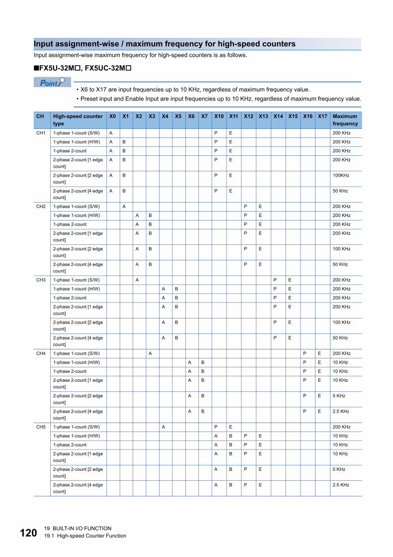
12019 BUILT-IN I/O FUNCTION
19.1 High-speed Counter Function
Input assignment-wise / maximum frequency for high-speed counters
Input assignment-wise maximum frequency for high-speed counters is as follows.
■FX5U-32M, FX5UC-32M
� X6 to X17 are input frequencies up to 10 KHz, regardless of maximum frequency value.
� Preset input and Enable Input are input frequencies up to 10 KHz, regardless of maximum frequency value.
CH High-speed counter
type
X0 X1 X2 X3 X4 X5 X6 X7 X10 X11 X12 X13 X14 X15 X16 X17 Maximum
frequency
CH1 1-phase 1-count (S/W) A P E 200 KHz
1-phase 1-count (H/W) A B P E 200 KHz
1-phase 2-count A B P E 200 KHz
2-phase 2-count [1 edge
count]
A B P E 200 KHz
2-phase 2-count [2 edge
count]
A B P E 100KHz
2-phase 2-count [4 edge
count]
A B P E 50 KHz
CH2 1-phase 1-count (S/W) A P E 200 KHz
1-phase 1-count (H/W) A B P E 200 KHz
1-phase 2-count A B P E 200 KHz
2-phase 2-count [1 edge
count]
A B P E 200 KHz
2-phase 2-count [2 edge
count]
A B P E 100 KHz
2-phase 2-count [4 edge
count]
A B P E 50 KHz
CH3 1-phase 1-count (S/W) A P E 200 KHz
1-phase 1-count (H/W) A B P E 200 KHz
1-phase 2-count A B P E 200 KHz
2-phase 2-count [1 edge
count]
A B P E 200 KHz
2-phase 2-count [2 edge
count]
A B P E 100 KHz
2-phase 2-count [4 edge
count]
A B P E 50 KHz
CH4 1-phase 1-count (S/W) A P E 200 KHz
1-phase 1-count (H/W) A B P E 10 KHz
1-phase 2-count A B P E 10 KHz
2-phase 2-count [1 edge
count]
A B P E 10 KHz
2-phase 2-count [2 edge
count]
A B P E 5 KHz
2-phase 2-count [4 edge
count]
A B P E 2.5 KHz
CH5 1-phase 1-count (S/W) A P E 200 KHz
1-phase 1-count (H/W) A B P E 10 KHz
1-phase 2-count A B P E 10 KHz
2-phase 2-count [1 edge
count]
A B P E 10 KHz
2-phase 2-count [2 edge
count]
A B P E 5 KHz
2-phase 2-count [4 edge
count]
A B P E 2.5 KHz
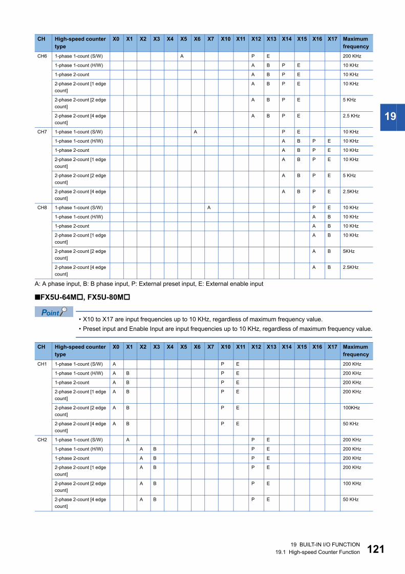
19 BUILT-IN I/O FUNCTION
19.1 High-speed Counter Function 121
19
A: A phase input, B: B phase input, P: External preset input, E: External enable input
■FX5U-64M, FX5U-80M
� X10 to X17 are input frequencies up to 10 KHz, regardless of maximum frequency value.
� Preset input and Enable Input are input frequencies up to 10 KHz, regardless of maximum frequency value.
CH6 1-phase 1-count (S/W) A P E 200 KHz
1-phase 1-count (H/W) A B P E 10 KHz
1-phase 2-count A B P E 10 KHz
2-phase 2-count [1 edge
count]
A B P E 10 KHz
2-phase 2-count [2 edge
count]
A B P E 5 KHz
2-phase 2-count [4 edge
count]
A B P E 2.5 KHz
CH7 1-phase 1-count (S/W) A P E 10 KHz
1-phase 1-count (H/W) A B P E 10 KHz
1-phase 2-count A B P E 10 KHz
2-phase 2-count [1 edge
count]
A B P E 10 KHz
2-phase 2-count [2 edge
count]
A B P E 5 KHz
2-phase 2-count [4 edge
count]
A B P E 2.5KHz
CH8 1-phase 1-count (S/W) A P E 10 KHz
1-phase 1-count (H/W) A B 10 KHz
1-phase 2-count A B 10 KHz
2-phase 2-count [1 edge
count]
A B 10 KHz
2-phase 2-count [2 edge
count]
A B 5KHz
2-phase 2-count [4 edge
count]
A B 2.5KHz
CH High-speed counter
type
X0 X1 X2 X3 X4 X5 X6 X7 X10 X11 X12 X13 X14 X15 X16 X17 Maximum
frequency
CH1 1-phase 1-count (S/W) A P E 200 KHz
1-phase 1-count (H/W) A B P E 200 KHz
1-phase 2-count A B P E 200 KHz
2-phase 2-count [1 edge
count]
A B P E 200 KHz
2-phase 2-count [2 edge
count]
A B P E 100KHz
2-phase 2-count [4 edge
count]
A B P E 50 KHz
CH2 1-phase 1-count (S/W) A P E 200 KHz
1-phase 1-count (H/W) A B P E 200 KHz
1-phase 2-count A B P E 200 KHz
2-phase 2-count [1 edge
count]
A B P E 200 KHz
2-phase 2-count [2 edge
count]
A B P E 100 KHz
2-phase 2-count [4 edge
count]
A B P E 50 KHz
CH High-speed counter
type
X0 X1 X2 X3 X4 X5 X6 X7 X10 X11 X12 X13 X14 X15 X16 X17 Maximum
frequency
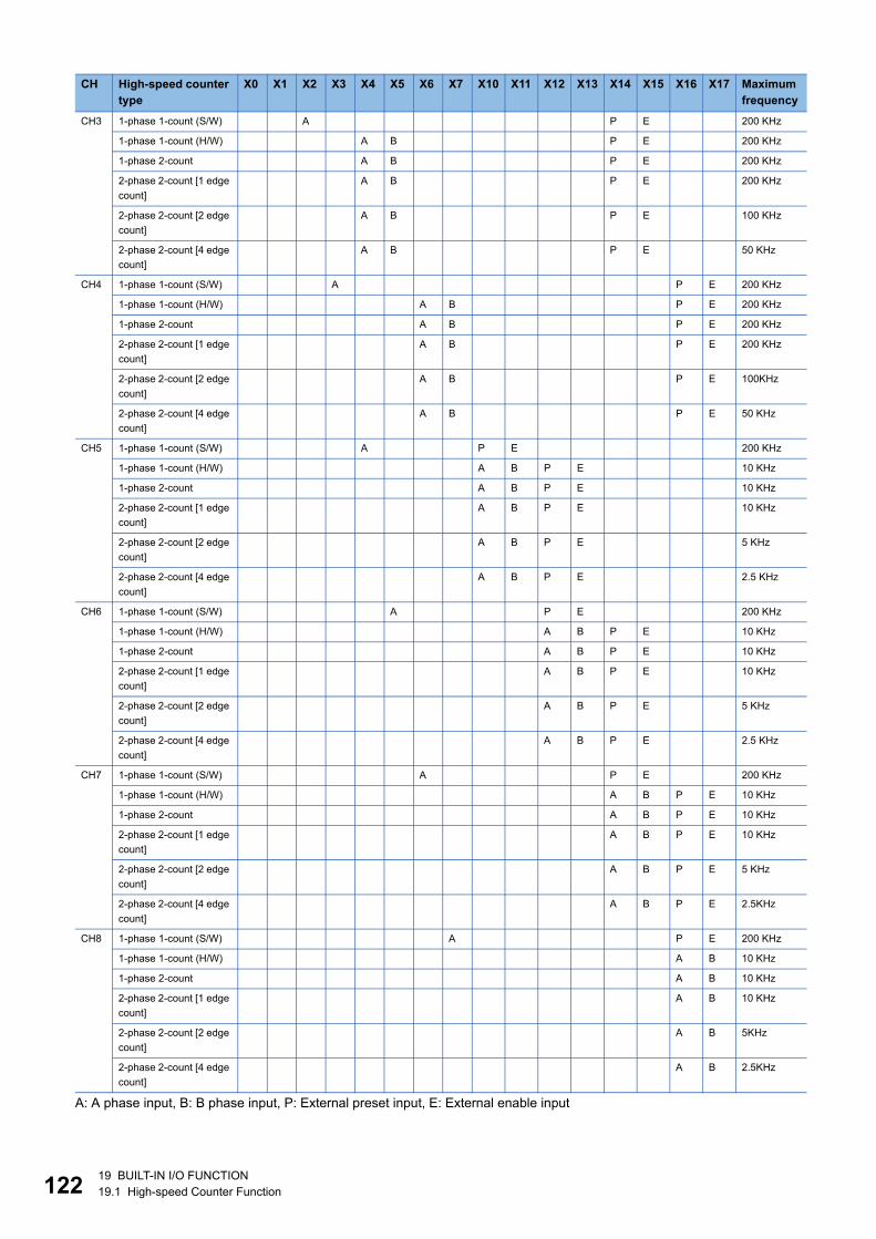
12219 BUILT-IN I/O FUNCTION
19.1 High-speed Counter Function
A: A phase input, B: B phase input, P: External preset input, E: External enable input
CH3 1-phase 1-count (S/W) A P E 200 KHz
1-phase 1-count (H/W) A B P E 200 KHz
1-phase 2-count A B P E 200 KHz
2-phase 2-count [1 edge
count]
A B P E 200 KHz
2-phase 2-count [2 edge
count]
A B P E 100 KHz
2-phase 2-count [4 edge
count]
A B P E 50 KHz
CH4 1-phase 1-count (S/W) A P E 200 KHz
1-phase 1-count (H/W) A B P E 200 KHz
1-phase 2-count A B P E 200 KHz
2-phase 2-count [1 edge
count]
A B P E 200 KHz
2-phase 2-count [2 edge
count]
A B P E 100KHz
2-phase 2-count [4 edge
count]
A B P E 50 KHz
CH5 1-phase 1-count (S/W) A P E 200 KHz
1-phase 1-count (H/W) A B P E 10 KHz
1-phase 2-count A B P E 10 KHz
2-phase 2-count [1 edge
count]
A B P E 10 KHz
2-phase 2-count [2 edge
count]
A B P E 5 KHz
2-phase 2-count [4 edge
count]
A B P E 2.5 KHz
CH6 1-phase 1-count (S/W) A P E 200 KHz
1-phase 1-count (H/W) A B P E 10 KHz
1-phase 2-count A B P E 10 KHz
2-phase 2-count [1 edge
count]
A B P E 10 KHz
2-phase 2-count [2 edge
count]
A B P E 5 KHz
2-phase 2-count [4 edge
count]
A B P E 2.5 KHz
CH7 1-phase 1-count (S/W) A P E 200 KHz
1-phase 1-count (H/W) A B P E 10 KHz
1-phase 2-count A B P E 10 KHz
2-phase 2-count [1 edge
count]
A B P E 10 KHz
2-phase 2-count [2 edge
count]
A B P E 5 KHz
2-phase 2-count [4 edge
count]
A B P E 2.5KHz
CH8 1-phase 1-count (S/W) A P E 200 KHz
1-phase 1-count (H/W) A B 10 KHz
1-phase 2-count A B 10 KHz
2-phase 2-count [1 edge
count]
A B 10 KHz
2-phase 2-count [2 edge
count]
A B 5KHz
2-phase 2-count [4 edge
count]
A B 2.5KHz
CH High-speed counter
type
X0 X1 X2 X3 X4 X5 X6 X7 X10 X11 X12 X13 X14 X15 X16 X17 Maximum
frequency
19 BUILT-IN I/O FUNCTION
19.1 High-speed Counter Function 123
19
High-speed counter parameters
High-speed counter parameters are explained below.
High-speed counter parameters are set by GX Works3.
Outline of parameters
High-speed counter settings, high-speed comparison table, multiple point high-speed comparison table setting and input
response time are set by parameters.
The primary items that can be set by parameters are as follows.
� Basic settings
� High-speed comparison table setting
� Multiple point output high-speed table setting
� Input response time setting
Parameter setting
High-speed counter parameter setting method is explained below.
For parameter setting of each operation, refer to the following.
� For high-speed counters (normal mode), refer to Page 124 High-speed counter (normal mode).
� For high-speed counter (pulse density measurement mode), refer to Page 126 High-speed counter (pulse density
measurement mode).
� For high-speed counter (rotational speed measurement mode), refer to Page 129 High-speed counter (rotational
speed measurement mode).
� For high-speed comparison table, refer to Page 132 High-speed comparison table.
� For multiple point output, high-speed comparison tables, refer to Page 134 Multiple point output, high-speed
comparison tables.
� For input response time, refer to Page 191 General-purpose Input Functions.
Parameters are enabled when the CPU module is powered ON or after a reset. In addition, operations
different from the parameter settings are possible by transferring values to special relays and special registers
while changing these values in the program.
For details concerning special relays and specials registers for high-speed counters, refer to Page 137
Special relay list, Page 148 Special registers list.
12419 BUILT-IN I/O FUNCTION
19.1 High-speed Counter Function
High-speed counter (normal mode)
Normal mode for high-speed counters is explained below.
Use normal mode if you want to use as an ordinary high-speed counter.
Set operation mode to normal mode by high-speed counter parameter setting.
Sets detailed settings for channel used.
Navigation window [Parameter] [FX5UCPU] [Module Parameter] [High Speed I/O] “Input Function" “High
Speed Counter" "Detail Setting" “Basic Settings"
Window
Displayed items
Item Description Setting range Default
Use/Not Use Set whether use counter or not. � Disable
� Enable
Disable
Operation Mode Set operation mode. � Normal Mode
� Pulse Density Assumption Mode
� Rotation Speed Measurement
Mode
Pulse Input Mode Set pulse input mode. � 1-Phase 1 Input (S/W Up/Down
Switch)
� 1-Phase 1 Input (H/W Up/Down
Switch)
� 1 Phase 2 Input
� 2 Phase 1 Multiple
� 2 Phase 2 Multiple
� 2 Phase 4 Multiple
� Internal Clock (1MHz)
Preset Input Enable/
Disable
Set whether to "enable" or "disable" the preset input of counter. � Disable
� Enable
Input Logic Sets preset input logic when preset input is enabled. � Positive Logic
� Negative Logic
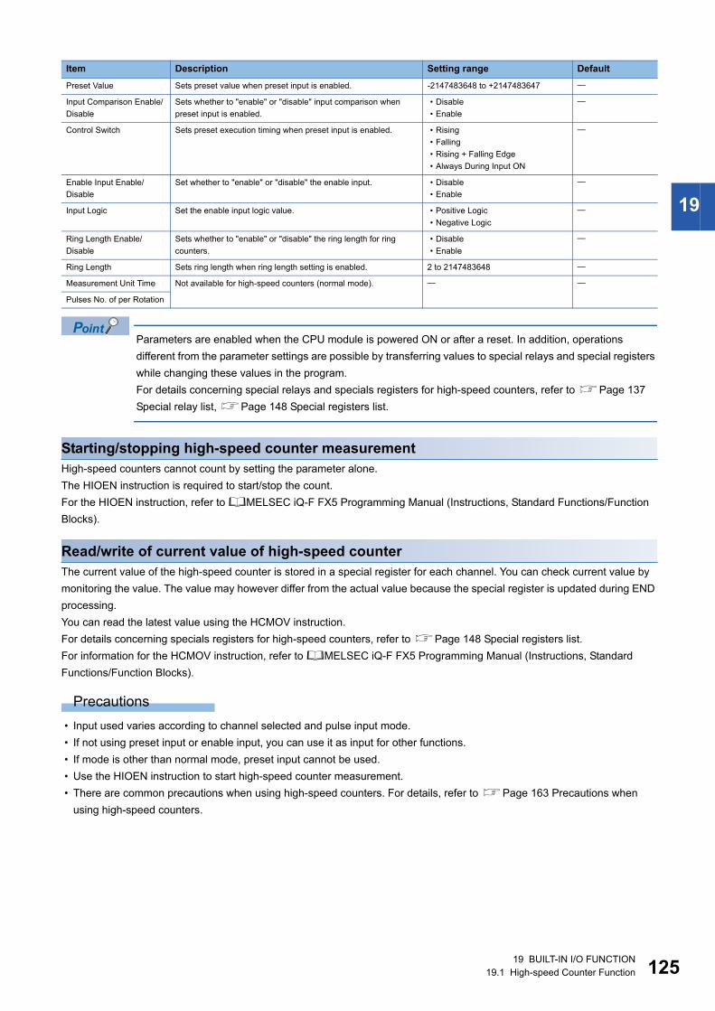
19 BUILT-IN I/O FUNCTION
19.1 High-speed Counter Function 125
19
Parameters are enabled when the CPU module is powered ON or after a reset. In addition, operations
different from the parameter settings are possible by transferring values to special relays and special registers
while changing these values in the program.
For details concerning special relays and specials registers for high-speed counters, refer to Page 137
Special relay list, Page 148 Special registers list.
Starting/stopping high-speed counter measurement
High-speed counters cannot count by setting the parameter alone.
The HIOEN instruction is required to start/stop the count.
For the HIOEN instruction, refer to MELSEC iQ-F FX5 Programming Manual (Instructions, Standard Functions/Function
Blocks).
Read/write of current value of high-speed counter
The current value of the high-speed counter is stored in a special register for each channel. You can check current value by
monitoring the value. The value may however differ from the actual value because the special register is updated during END
processing.
You can read the latest value using the HCMOV instruction.
For details concerning specials registers for high-speed counters, refer to Page 148 Special registers list.
For information for the HCMOV instruction, refer to MELSEC iQ-F FX5 Programming Manual (Instructions, Standard
Functions/Function Blocks).
Precautions
� Input used varies according to channel selected and pulse input mode.
� If not using preset input or enable input, you can use it as input for other functions.
� If mode is other than normal mode, preset input cannot be used.
� Use the HIOEN instruction to start high-speed counter measurement.
� There are common precautions when using high-speed counters. For details, refer to Page 163 Precautions when
using high-speed counters.
Preset Value Sets preset value when preset input is enabled. -2147483648 to +2147483647
Input Comparison Enable/
Disable
Sets whether to "enable" or "disable" input comparison when
preset input is enabled.
� Disable
� Enable
Control Switch Sets preset execution timing when preset input is enabled. � Rising
� Falling
� Rising + Falling Edge
� Always During Input ON
Enable Input Enable/
Disable
Set whether to "enable" or "disable" the enable input. � Disable
� Enable
Input Logic Set the enable input logic value. � Positive Logic
� Negative Logic
Ring Length Enable/
Disable
Sets whether to "enable" or "disable" the ring length for ring
counters.
� Disable
� Enable
Ring Length Sets ring length when ring length setting is enabled. 2 to 2147483648
Measurement Unit Time Not available for high-speed counters (normal mode).
Pulses No. of per Rotation
Item Description Setting range Default
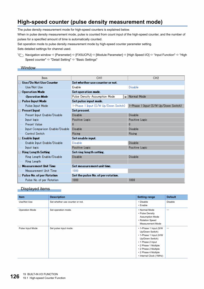
12619 BUILT-IN I/O FUNCTION
19.1 High-speed Counter Function
High-speed counter (pulse density measurement mode)
The pulse density measurement mode for high-speed counters is explained below.
When in pulse density measurement mode, pulse is counted from count input of the high-speed counter, and the number of
pulses for a specified amount of time is automatically counted.
Set operation mode to pulse density measurement mode by high-speed counter parameter setting.
Sets detailed settings for channel used.
Navigation window [Parameter] [FX5UCPU] [Module Parameter] [High Speed I/O] “Input Function" “High
Speed counter" "Detail Setting" “Basic Settings"
Window
Displayed items
Item Description Setting range Default
Use/Not Use Set whether use counter or not. � Disable
� Enable
Disable
Operation Mode Set operation mode. � Normal Mode
� Pulse Density
Assumption Mode
� Rotation Speed
Measurement Mode
Pulse Input Mode Set pulse input mode. � 1-Phase 1 Input (S/W
Up/Down Switch)
� 1-Phase 1 Input (H/W
Up/Down Switch)
� 1 Phase 2 Input
� 2 Phase 1 Multiple
� 2 Phase 2 Multiple
� 2 Phase 4 Multiple
� Internal Clock (1MHz)
19 BUILT-IN I/O FUNCTION
19.1 High-speed Counter Function 127
19
Parameters are enabled when the CPU module is powered ON or after a reset. In addition, operations
different from the parameter settings are possible by transferring values to special relays and special registers
while changing these values in the program.
For details concerning special relays and specials registers for high-speed counters, refer to Page 137
Special relay list, Page 148 Special registers list.
Pulse density measurement mode start/stop
The pulse density measurement mode cannot measure by setting the parameter alone.
The HIOEN instruction is required to start/stop measurement.
For the HIOEN instruction, refer to MELSEC iQ-F FX5 Programming Manual (Instructions, Standard Functions/Function
Blocks).
Pulse density
Pulse density is stored in the special register for each channel.
For details concerning specials registers for high-speed counters, refer to Page 148 Special registers list.
Preset Input Enable/
Disable
Not available for high-speed counters (pulse density measurement mode).
Input Logic
Preset Value
Input Comparison Enable/
Disable
Control Switch
Enable Input Enable/
Disable
Set whether to "enable" or "disable" the enable input. � Disable
� Enable
Input Logic Set the enable input logic value. � Positive Logic
� Negative Logic
Ring Length Enable/
Disable
Not available for high-speed counters (pulse density measurement mode).
Ring Length
Measurement Unit Time Set measurement unit time. (Unit: ms) 1 to 2147483647
Pulses No. of per Rotation Not available for high-speed counters (pulse density measurement mode).
Item Description Setting range Default
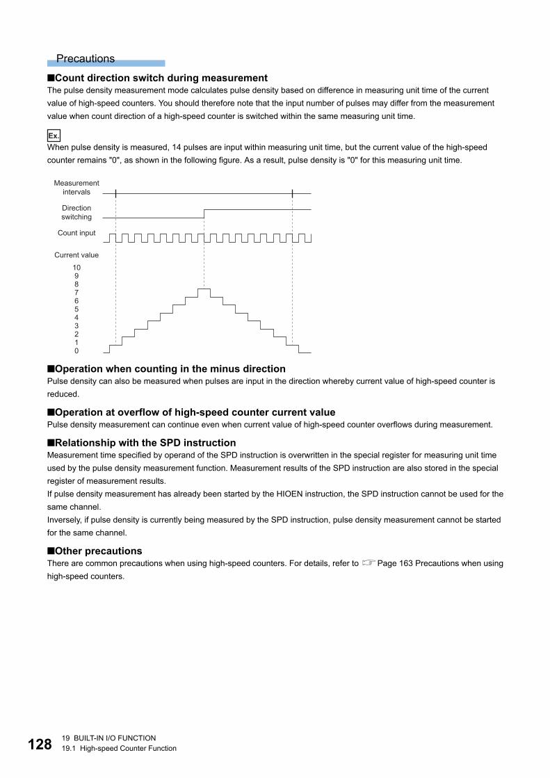
12819 BUILT-IN I/O FUNCTION
19.1 High-speed Counter Function
Precautions
■Count direction switch during measurementThe pulse density measurement mode calculates pulse density based on difference in measuring unit time of the current
value of high-speed counters. You should therefore note that the input number of pulses may differ from the measurement
value when count direction of a high-speed counter is switched within the same measuring unit time.
Ex.
When pulse density is measured, 14 pulses are input within measuring unit time, but the current value of the high-speed
counter remains "0", as shown in the following figure. As a result, pulse density is "0" for this measuring unit time.
■Operation when counting in the minus directionPulse density can also be measured when pulses are input in the direction whereby current value of high-speed counter is
reduced.
■Operation at overflow of high-speed counter current valuePulse density measurement can continue even when current value of high-speed counter overflows during measurement.
■Relationship with the SPD instructionMeasurement time specified by operand of the SPD instruction is overwritten in the special register for measuring unit time
used by the pulse density measurement function. Measurement results of the SPD instruction are also stored in the special
register of measurement results.
If pulse density measurement has already been started by the HIOEN instruction, the SPD instruction cannot be used for the
same channel.
Inversely, if pulse density is currently being measured by the SPD instruction, pulse density measurement cannot be started
for the same channel.
■Other precautionsThere are common precautions when using high-speed counters. For details, refer to Page 163 Precautions when using
high-speed counters.
Measurement
intervals
Direction
switching
Count input
Current value
109876543210
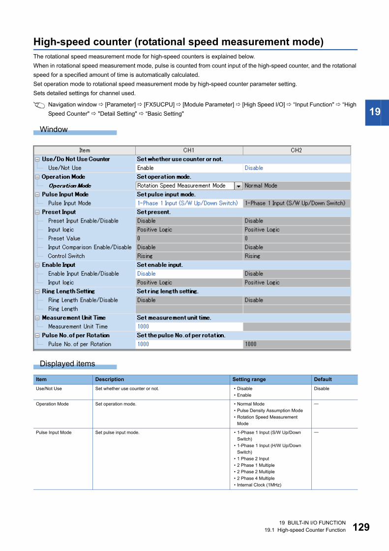
19 BUILT-IN I/O FUNCTION
19.1 High-speed Counter Function 129
19
High-speed counter (rotational speed measurement mode)
The rotational speed measurement mode for high-speed counters is explained below.
When in rotational speed measurement mode, pulse is counted from count input of the high-speed counter, and the rotational
speed for a specified amount of time is automatically calculated.
Set operation mode to rotational speed measurement mode by high-speed counter parameter setting.
Sets detailed settings for channel used.
Navigation window [Parameter] [FX5UCPU] [Module Parameter] [High Speed I/O] “Input Function" “High
Speed Counter" "Detail Setting" “Basic Setting"
Window
Displayed items
Item Description Setting range Default
Use/Not Use Set whether use counter or not. � Disable
� Enable
Disable
Operation Mode Set operation mode. � Normal Mode
� Pulse Density Assumption Mode
� Rotation Speed Measurement
Mode
Pulse Input Mode Set pulse input mode. � 1-Phase 1 Input (S/W Up/Down
Switch)
� 1-Phase 1 Input (H/W Up/Down
Switch)
� 1 Phase 2 Input
� 2 Phase 1 Multiple
� 2 Phase 2 Multiple
� 2 Phase 4 Multiple
� Internal Clock (1MHz)
13019 BUILT-IN I/O FUNCTION
19.1 High-speed Counter Function
Parameters are enabled when the CPU module is powered ON or after a reset. In addition, operations
different from the parameter settings are possible by transferring values to special relays and special registers
while changing these values in the program.
For details concerning special relays and specials registers for high-speed counters, refer to Page 137
Special relay list, Page 148 Special registers list.
Rotational speed measurement mode start/stop
The rotational speed measurement mode cannot measure by setting the parameter alone.
The HIOEN instruction is required to start/stop measurement.
For the HIOEN instruction, refer to MELSEC iQ-F FX5 Programming Manual (Instructions, Standard Functions/Function
Blocks).
Rotational speed
Rotational speed is stored in the special register for each channel.
For details concerning specials registers for high-speed counters, refer to Page 148 Special registers list.
Preset Input Enable/
Disable
Not available for high-speed counters (rotational speed
measurement mode).
Input Logic
Preset Value
Input Comparison Enable/
Disable
Control Switch
Enable Input Enable/
Disable
Set whether to "enable" or "disable" the enable input. � Disable
� Enable
Input Logic Set the enable input logic value. � Positive Logic
� Negative Logic
Ring Length Enable/
Disable
Not available for high-speed counters (rotational speed
measurement mode).
Ring Length
Measurement Unit Time Set measurement unit time. (Unit: ms) 1 to 2147483647
Pulses No. of per Rotation Set the No. of pulses per rotation. (Unit: ms) 1 to 2147483647
Item Description Setting range Default
19 BUILT-IN I/O FUNCTION
19.1 High-speed Counter Function 131
19
Precautions
■Count direction switch during measurementThe rotational speed measurement mode calculates rotational speed based on current value difference of high-speed
counters in the measuring unit time. You should therefore note that the input number of pulses may differ from the
measurement value when count direction of a high-speed counter is switched within the same measuring unit time.
■Operation when counting in the minus directionRotational speed can also be measured when pulses are input in the direction whereby current value of high-speed counter is
reduced.
■Operation at overflow of high-speed counter current valueRotational speed measurement can continue even when current value of high-speed counter overflows during measurement.
■Relationship with the SPD instructionMeasurement time specified by operand of the SPD instruction is written in the special register for measuring unit time used
by the rotational speed measurement function. Measurement results of the SPD instruction are also stored in the special
register of measurement results.
If rotational speed measurement has already been started by the HIOEN instruction, the SPD instruction cannot be used for
the same channel.
Inversely, if pulse density is currently being measured by the SPD instruction, rotational speed measurement cannot be
started for the same channel.
■Other precautionsThere are common precautions when using high-speed counters. For details, refer to Page 163 Precautions when using
high-speed counters.
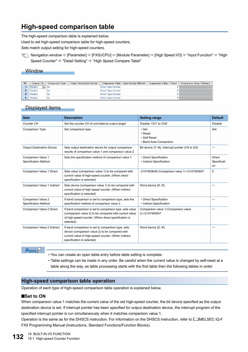
13219 BUILT-IN I/O FUNCTION
19.1 High-speed Counter Function
High-speed comparison table
The high-speed comparison table is explained below.
Used to set high-speed comparison table for high-speed counters.
Sets match output setting for high-speed counters.
Navigation window [Parameter] [FX5UCPU] [Module Parameter] [High Speed I/O] “Input Function" “High
Speed Counter" "Detail Setting" “High Speed Compare Table"
Window
Displayed items
� You can create an open table entry before table setting is complete.
� Table settings can be made in any order. Be careful when the current value is changed by self-reset at a
table along the way, as table processing starts with the first table then the following tables in order.
High-speed comparison table operation
Operation of each type of high-speed comparison table operation is explained below.
■Set to ONWhen comparison value 1 matches the current value of the set high-speed counter, the bit device specified as the output
destination device is set. If interrupt pointer has been specified for output destination device, the interrupt program of the
specified interrupt pointer is run simultaneously when it matches comparison value 1.
Operation is the same as for the DHSCS instruction. For information on the DHSCS instruction, refer to MELSEC iQ-F
FX5 Programming Manual (Instructions, Standard Functions/Function Blocks).
Item Description Setting range Default
Counter CH Set the counter CH of coincidence output target. Disable, CH1 to CH8 Disable
Comparison Type Set comparison type. � Set
� Reset
� Self Reset
� Band Area Comparison
Set
Output Destination Device Sets output destination device for output comparison
results of comparison value 1 and comparison value 2.
Bit device (Y, M), Interrupt pointer (I16 to I23)
Comparison Value 1
Specification Method
Sets the specification method of comparison value 1. � Direct Specification
� Indirect Specification
Direct
Specificati
on
Comparison Value 1 Direct Sets value (comparison value 1) to be compared with
current value of high-speed counter. (When direct
specification is selected)
-2147483648Comparison value 1+2147483647 0
Comparison Value 1 Indirect Sets device (comparison value 1) to be compared with
current value of high-speed counter. (When indirect
specification is selected)
Word device (D, R)
Comparison Value 2
Specification Method
If band comparison is set to comparison type, sets the
specification method of comparison value 2.
� Direct Specification
� Indirect Specification
Comparison Value 2 Direct If band comparison is set to comparison type, sets value
(comparison value 2) to be compared with current value
of high-speed counter. (When direct specification is
selected)
Comparison value 1Comparison value
2+2147483647
Comparison Value 2 Indirect If band comparison is set to comparison type, sets
device (comparison value 2) to be compared with
current value of high-speed counter. (When indirect
specification is selected)
Word device (D, R)
19 BUILT-IN I/O FUNCTION
19.1 High-speed Counter Function 133
19
■ResetWhen comparison value 1 matches the current value of the set high-speed counter, the bit device specified as the output
destination device is reset.
Operation is the same as for the DHSCR instruction. For information on the DHSCR instruction, refer to MELSEC iQ-F
FX5 Programming Manual (Instructions, Standard Functions/Function Blocks).
■Self-resetWhen comparison value 1 matches the current value of the set high-speed counter, the current value becomes the preset
value. When the preset value is set by self-reset, comparison processing is not performed.
Operation is the same as self-reset for the DHSCR instruction. For information on the DHSCR instruction, refer to
MELSEC iQ-F FX5 Programming Manual (Instructions, Standard Functions/Function Blocks).
■Zone CompareBased on the current high-speed counter value, comparison value 1, and comparison value 3, one of the three output devices
from the head output device will be set. The rest are reset.
Operation is the same as for the DHSZ instruction. For information on zone comparison and DHSZ instruction, refer to
MELSEC iQ-F FX5 Programming Manual (Instructions, Standard Functions/Function Blocks).
Comparison start/stop for high-speed comparison table
High-speed comparison tables cannot execute comparison by setting the parameter alone.
The HIOEN instruction is required to start/stop the high-speed comparison table.
For the HIOEN instruction, refer to MELSEC iQ-F FX5 Programming Manual (Instructions, Standard Functions/Function
Blocks).
The DHIOEN instruction is required to start/stop high-speed counters as well when using a high-speed
comparison table.
Measurement is not conducted by starting the high-speed comparison table alone, and the high-speed
comparison table therefore does not operate.
Precautions
■Number of tables that can be setUp to 4 tables can be set. Empty tables are not included in the number of tables.
■Processing orderHigh-speed comparison tables are processed in sequence starting from the first table.
■Operation start timingHigh-speed comparison tables are updated during END processing. If started/stopped by the DHIOEN instruction, the table is
applied starting from the next scan. Caution must be exercised when controlling high-speed comparison tables using the
DHIOEN instruction several times within the same scan.
Ex.
Table operation is as follows when multiple DHIOEN instructions are executed within the same scan.
Tables 1, 2 and 4 are started at the 1st DHIOEN instruction.
Tables 3 and 5 are started, and 2 and 4 are stopped at the 2nd DHIOEN instruction.
Table 2 is started and 5 is stopped at the 3rd DHIOEN instruction.
Tables 1, 2 and 3 operate.
■Operation when using internal clockSelf-reset cannot be used for channels set to internal clock by pulse input mode.
Comparison value 1 Current value Head output device
Comparison value 1 Current value Comparison value 2 Head output device +1
Current value Comparison value 2 Head output device +2
Set
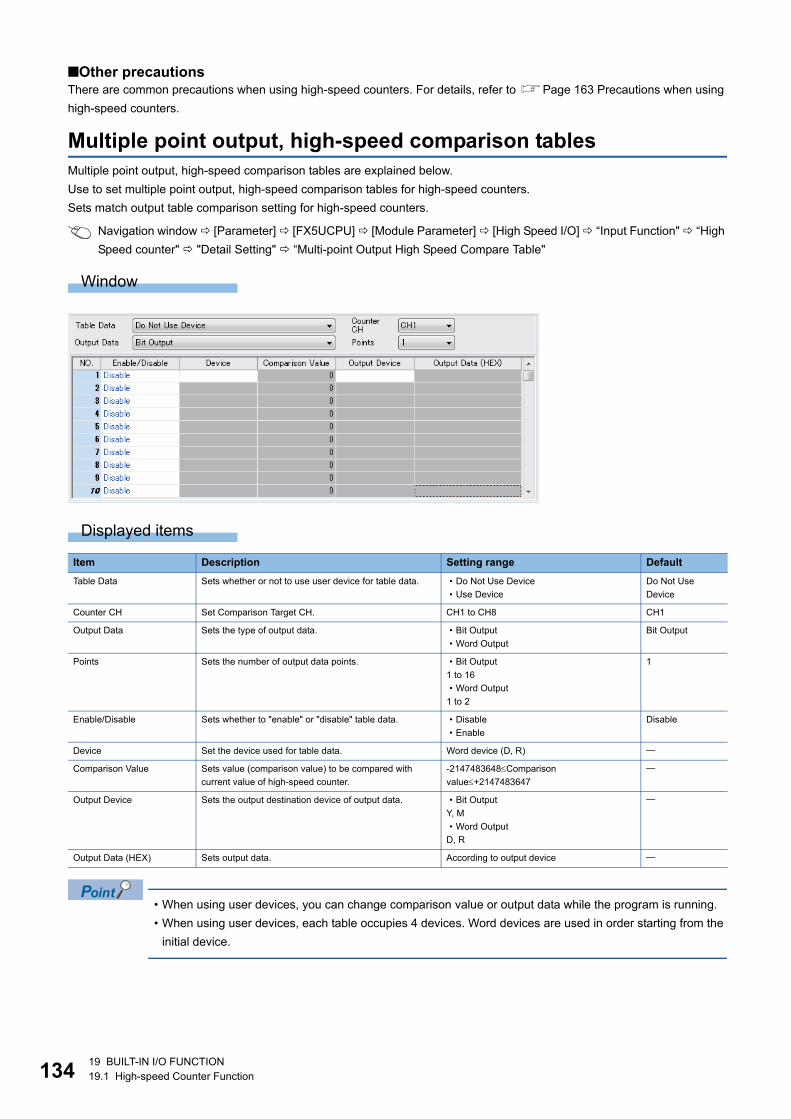
13419 BUILT-IN I/O FUNCTION
19.1 High-speed Counter Function
■Other precautionsThere are common precautions when using high-speed counters. For details, refer to Page 163 Precautions when using
high-speed counters.
Multiple point output, high-speed comparison tables
Multiple point output, high-speed comparison tables are explained below.
Use to set multiple point output, high-speed comparison tables for high-speed counters.
Sets match output table comparison setting for high-speed counters.
Navigation window [Parameter] [FX5UCPU] [Module Parameter] [High Speed I/O] “Input Function" “High
Speed counter" "Detail Setting" “Multi-point Output High Speed Compare Table"
Window
Displayed items
� When using user devices, you can change comparison value or output data while the program is running.
� When using user devices, each table occupies 4 devices. Word devices are used in order starting from the
initial device.
Item Description Setting range Default
Table Data Sets whether or not to use user device for table data. � Do Not Use Device
� Use Device
Do Not Use
Device
Counter CH Set Comparison Target CH. CH1 to CH8 CH1
Output Data Sets the type of output data. � Bit Output
� Word Output
Bit Output
Points Sets the number of output data points. � Bit Output
1 to 16
� Word Output
1 to 2
1
Enable/Disable Sets whether to "enable" or "disable" table data. � Disable
� Enable
Disable
Device Set the device used for table data. Word device (D, R)
Comparison Value Sets value (comparison value) to be compared with
current value of high-speed counter.
-2147483648Comparison
value+2147483647
Output Device Sets the output destination device of output data. � Bit Output
Y, M
� Word Output
D, R
Output Data (HEX) Sets output data. According to output device
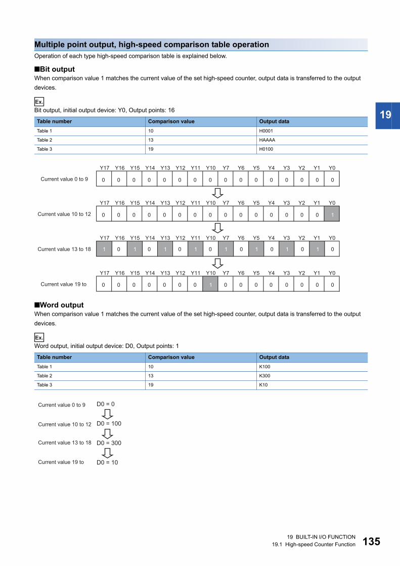
19 BUILT-IN I/O FUNCTION
19.1 High-speed Counter Function 135
19
Multiple point output, high-speed comparison table operation
Operation of each type high-speed comparison table is explained below.
■Bit outputWhen comparison value 1 matches the current value of the set high-speed counter, output data is transferred to the output
devices.
Ex.
Bit output, initial output device: Y0, Output points: 16
■Word outputWhen comparison value 1 matches the current value of the set high-speed counter, output data is transferred to the output
devices.
Ex.
Word output, initial output device: D0, Output points: 1
Table number Comparison value Output data
Table 1 10 H0001
Table 2 13 HAAAA
Table 3 19 H0100
Table number Comparison value Output data
Table 1 10 K100
Table 2 13 K300
Table 3 19 K10
Y0Y1Y2Y3Y4Y5Y6Y7Y10Y11Y12Y13Y14Y15Y16Y17
0 0 0 0 0 0 0 0 0 01 00 0 0 0
011 1 1 1 0 1 0 1 0 10 0 0 0
0 0 0 0 0 0 0 0 0 0 0 0 0 0 0 1
0 0 0 0 0 0 0 0 0 0 0 0 0 0 0 0Current value 0 to 9
Y0Y1Y2Y3Y4Y5Y6Y7Y10Y11Y12Y13Y14Y15Y16Y17
Current value 10 to 12
Y0Y1Y2Y3Y4Y5Y6Y7Y10Y11Y12Y13Y14Y15Y16Y17
Current value 13 to 18
Y0Y1Y2Y3Y4Y5Y6Y7Y10Y11Y12Y13Y14Y15Y16Y17
Current value 19 to
Current value 0 to 9 D0 = 0
Current value 10 to 12 D0 = 100
Current value 13 to 18 D0 = 300
Current value 19 to D0 = 10
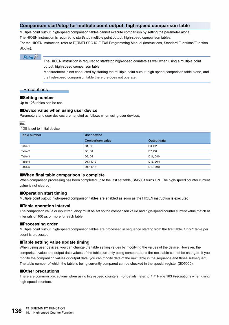
13619 BUILT-IN I/O FUNCTION
19.1 High-speed Counter Function
Comparison start/stop for multiple point output, high-speed comparison table
Multiple point output, high-speed comparison tables cannot execute comparison by setting the parameter alone.
The HIOEN instruction is required to start/stop multiple point output, high-speed comparison tables.
For the HIOEN instruction, refer to MELSEC iQ-F FX5 Programming Manual (Instructions, Standard Functions/Function
Blocks).
The HIOEN instruction is required to start/stop high-speed counters as well when using a multiple point
output, high-speed comparison table.
Measurement is not conducted by starting the multiple point output, high-speed comparison table alone, and
the high-speed comparison table therefore does not operate.
Precautions
■Setting numberUp to 128 tables can be set.
■Device value when using user deviceParameters and user devices are handled as follows when using user devices.
Ex.
If D0 is set to initial device
■When final table comparison is completeWhen comparison processing has been completed up to the last set table, SM5001 turns ON. The high-speed counter current
value is not cleared.
■Operation start timingMultiple point output, high-speed comparison tables are enabled as soon as the HIOEN instruction is executed.
■Table operation intervalThe comparison value or input frequency must be set so the comparison value and high-speed counter current value match at
intervals of 100 s or more for each table.
■Processing orderMultiple point output, high-speed comparison tables are processed in sequence starting from the first table. Only 1 table per
count is processed.
■Table setting value update timingWhen using user devices, you can change the table setting values by modifying the values of the device. However, the
comparison value and output data values of the table currently being compared and the next table cannot be changed. If you
modify the comparison values or output data, you can modify data of the next table in the sequence and those subsequent.
The table number of which the table is being currently compared can be checked in the special register (SD5000).
■Other precautionsThere are common precautions when using high-speed counters. For details, refer to Page 163 Precautions when using
high-speed counters.
Table number User device
Comparison value Output data
Table 1 D1, D0 D3, D2
Table 2 D5, D4 D7, D6
Table 3 D9, D8 D11, D10
Table 4 D13, D12 D15, D14
Table 5 D17, D16 D19, D18
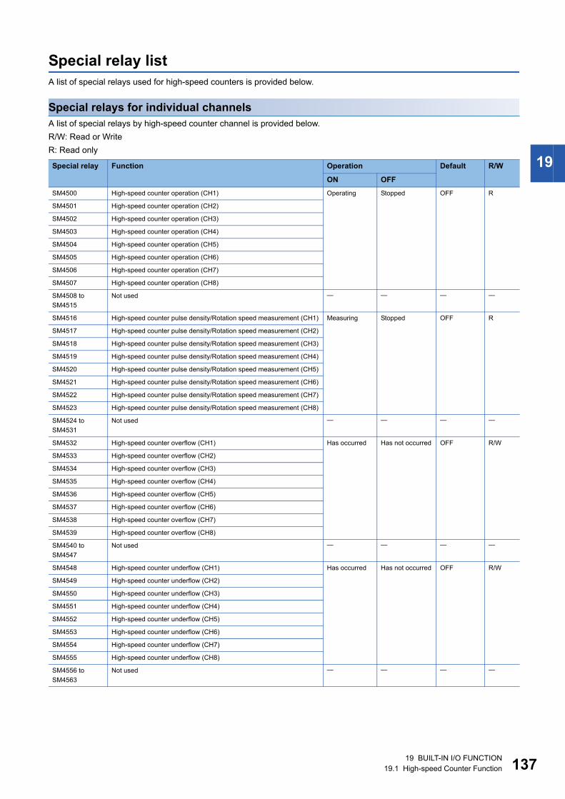
19 BUILT-IN I/O FUNCTION
19.1 High-speed Counter Function 137
19
Special relay list
A list of special relays used for high-speed counters is provided below.
Special relays for individual channels
A list of special relays by high-speed counter channel is provided below.
R/W: Read or Write
R: Read only
Special relay Function Operation Default R/W
ON OFF
SM4500 High-speed counter operation (CH1) Operating Stopped OFF R
SM4501 High-speed counter operation (CH2)
SM4502 High-speed counter operation (CH3)
SM4503 High-speed counter operation (CH4)
SM4504 High-speed counter operation (CH5)
SM4505 High-speed counter operation (CH6)
SM4506 High-speed counter operation (CH7)
SM4507 High-speed counter operation (CH8)
SM4508 to
SM4515
Not used
SM4516 High-speed counter pulse density/Rotation speed measurement (CH1) Measuring Stopped OFF R
SM4517 High-speed counter pulse density/Rotation speed measurement (CH2)
SM4518 High-speed counter pulse density/Rotation speed measurement (CH3)
SM4519 High-speed counter pulse density/Rotation speed measurement (CH4)
SM4520 High-speed counter pulse density/Rotation speed measurement (CH5)
SM4521 High-speed counter pulse density/Rotation speed measurement (CH6)
SM4522 High-speed counter pulse density/Rotation speed measurement (CH7)
SM4523 High-speed counter pulse density/Rotation speed measurement (CH8)
SM4524 to
SM4531
Not used
SM4532 High-speed counter overflow (CH1) Has occurred Has not occurred OFF R/W
SM4533 High-speed counter overflow (CH2)
SM4534 High-speed counter overflow (CH3)
SM4535 High-speed counter overflow (CH4)
SM4536 High-speed counter overflow (CH5)
SM4537 High-speed counter overflow (CH6)
SM4538 High-speed counter overflow (CH7)
SM4539 High-speed counter overflow (CH8)
SM4540 to
SM4547
Not used
SM4548 High-speed counter underflow (CH1) Has occurred Has not occurred OFF R/W
SM4549 High-speed counter underflow (CH2)
SM4550 High-speed counter underflow (CH3)
SM4551 High-speed counter underflow (CH4)
SM4552 High-speed counter underflow (CH5)
SM4553 High-speed counter underflow (CH6)
SM4554 High-speed counter underflow (CH7)
SM4555 High-speed counter underflow (CH8)
SM4556 to
SM4563
Not used
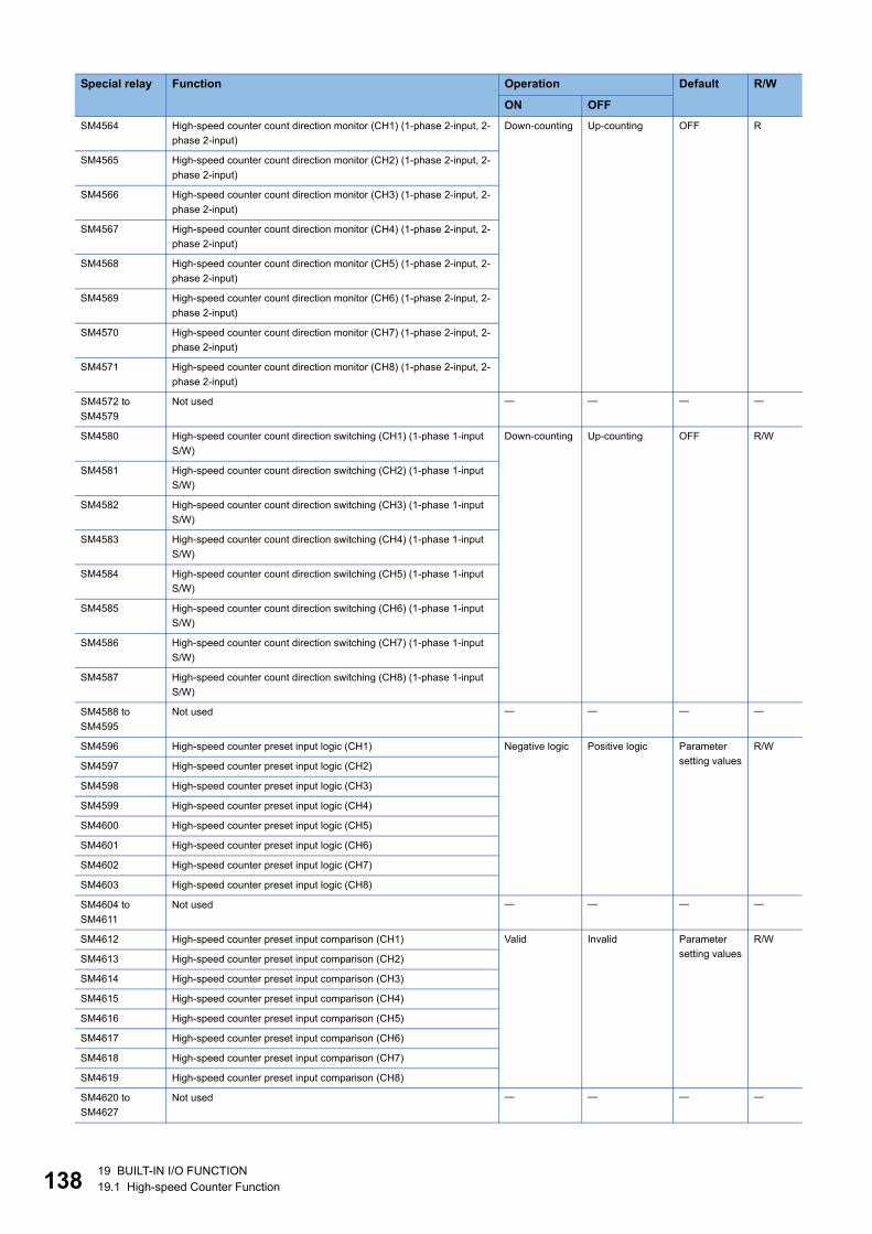
13819 BUILT-IN I/O FUNCTION
19.1 High-speed Counter Function
SM4564 High-speed counter count direction monitor (CH1) (1-phase 2-input, 2-
phase 2-input)
Down-counting Up-counting OFF R
SM4565 High-speed counter count direction monitor (CH2) (1-phase 2-input, 2-
phase 2-input)
SM4566 High-speed counter count direction monitor (CH3) (1-phase 2-input, 2-
phase 2-input)
SM4567 High-speed counter count direction monitor (CH4) (1-phase 2-input, 2-
phase 2-input)
SM4568 High-speed counter count direction monitor (CH5) (1-phase 2-input, 2-
phase 2-input)
SM4569 High-speed counter count direction monitor (CH6) (1-phase 2-input, 2-
phase 2-input)
SM4570 High-speed counter count direction monitor (CH7) (1-phase 2-input, 2-
phase 2-input)
SM4571 High-speed counter count direction monitor (CH8) (1-phase 2-input, 2-
phase 2-input)
SM4572 to
SM4579
Not used
SM4580 High-speed counter count direction switching (CH1) (1-phase 1-input
S/W)
Down-counting Up-counting OFF R/W
SM4581 High-speed counter count direction switching (CH2) (1-phase 1-input
S/W)
SM4582 High-speed counter count direction switching (CH3) (1-phase 1-input
S/W)
SM4583 High-speed counter count direction switching (CH4) (1-phase 1-input
S/W)
SM4584 High-speed counter count direction switching (CH5) (1-phase 1-input
S/W)
SM4585 High-speed counter count direction switching (CH6) (1-phase 1-input
S/W)
SM4586 High-speed counter count direction switching (CH7) (1-phase 1-input
S/W)
SM4587 High-speed counter count direction switching (CH8) (1-phase 1-input
S/W)
SM4588 to
SM4595
Not used
SM4596 High-speed counter preset input logic (CH1) Negative logic Positive logic Parameter
setting values
R/W
SM4597 High-speed counter preset input logic (CH2)
SM4598 High-speed counter preset input logic (CH3)
SM4599 High-speed counter preset input logic (CH4)
SM4600 High-speed counter preset input logic (CH5)
SM4601 High-speed counter preset input logic (CH6)
SM4602 High-speed counter preset input logic (CH7)
SM4603 High-speed counter preset input logic (CH8)
SM4604 to
SM4611
Not used
SM4612 High-speed counter preset input comparison (CH1) Valid Invalid Parameter
setting values
R/W
SM4613 High-speed counter preset input comparison (CH2)
SM4614 High-speed counter preset input comparison (CH3)
SM4615 High-speed counter preset input comparison (CH4)
SM4616 High-speed counter preset input comparison (CH5)
SM4617 High-speed counter preset input comparison (CH6)
SM4618 High-speed counter preset input comparison (CH7)
SM4619 High-speed counter preset input comparison (CH8)
SM4620 to
SM4627
Not used
Special relay Function Operation Default R/W
ON OFF
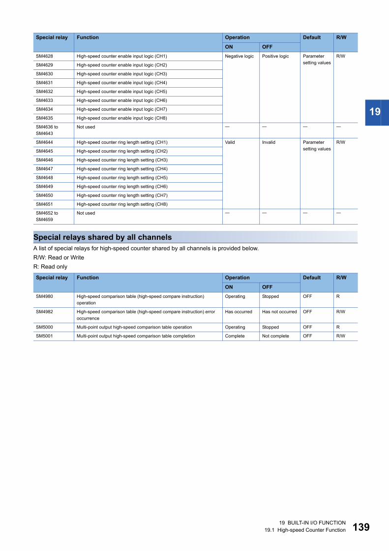
19 BUILT-IN I/O FUNCTION
19.1 High-speed Counter Function 139
19
Special relays shared by all channels
A list of special relays for high-speed counter shared by all channels is provided below.
R/W: Read or Write
R: Read only
SM4628 High-speed counter enable input logic (CH1) Negative logic Positive logic Parameter
setting values
R/W
SM4629 High-speed counter enable input logic (CH2)
SM4630 High-speed counter enable input logic (CH3)
SM4631 High-speed counter enable input logic (CH4)
SM4632 High-speed counter enable input logic (CH5)
SM4633 High-speed counter enable input logic (CH6)
SM4634 High-speed counter enable input logic (CH7)
SM4635 High-speed counter enable input logic (CH8)
SM4636 to
SM4643
Not used
SM4644 High-speed counter ring length setting (CH1) Valid Invalid Parameter
setting values
R/W
SM4645 High-speed counter ring length setting (CH2)
SM4646 High-speed counter ring length setting (CH3)
SM4647 High-speed counter ring length setting (CH4)
SM4648 High-speed counter ring length setting (CH5)
SM4649 High-speed counter ring length setting (CH6)
SM4650 High-speed counter ring length setting (CH7)
SM4651 High-speed counter ring length setting (CH8)
SM4652 to
SM4659
Not used
Special relay Function Operation Default R/W
ON OFF
SM4980 High-speed comparison table (high-speed compare instruction)
operation
Operating Stopped OFF R
SM4982 High-speed comparison table (high-speed compare instruction) error
occurrence
Has occurred Has not occurred OFF R/W
SM5000 Multi-point output high-speed comparison table operation Operating Stopped OFF R
SM5001 Multi-point output high-speed comparison table completion Complete Not complete OFF R/W
Special relay Function Operation Default R/W
ON OFF
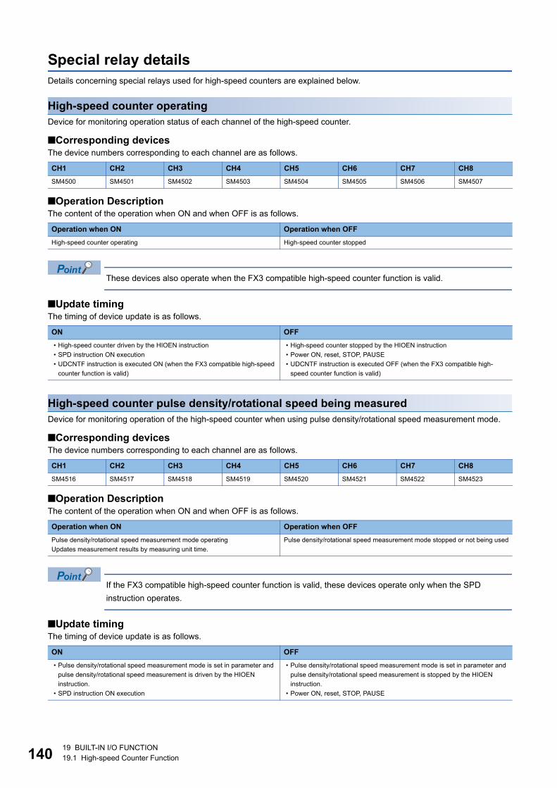
14019 BUILT-IN I/O FUNCTION
19.1 High-speed Counter Function
Special relay details
Details concerning special relays used for high-speed counters are explained below.
High-speed counter operating
Device for monitoring operation status of each channel of the high-speed counter.
■Corresponding devicesThe device numbers corresponding to each channel are as follows.
■Operation DescriptionThe content of the operation when ON and when OFF is as follows.
These devices also operate when the FX3 compatible high-speed counter function is valid.
■Update timingThe timing of device update is as follows.
High-speed counter pulse density/rotational speed being measured
Device for monitoring operation of the high-speed counter when using pulse density/rotational speed measurement mode.
■Corresponding devicesThe device numbers corresponding to each channel are as follows.
■Operation DescriptionThe content of the operation when ON and when OFF is as follows.
If the FX3 compatible high-speed counter function is valid, these devices operate only when the SPD
instruction operates.
■Update timingThe timing of device update is as follows.
CH1 CH2 CH3 CH4 CH5 CH6 CH7 CH8
SM4500 SM4501 SM4502 SM4503 SM4504 SM4505 SM4506 SM4507
Operation when ON Operation when OFF
High-speed counter operating High-speed counter stopped
ON OFF
� High-speed counter driven by the HIOEN instruction
� SPD instruction ON execution
� UDCNTF instruction is executed ON (when the FX3 compatible high-speed
counter function is valid)
� High-speed counter stopped by the HIOEN instruction
� Power ON, reset, STOP, PAUSE
� UDCNTF instruction is executed OFF (when the FX3 compatible high-
speed counter function is valid)
CH1 CH2 CH3 CH4 CH5 CH6 CH7 CH8
SM4516 SM4517 SM4518 SM4519 SM4520 SM4521 SM4522 SM4523
Operation when ON Operation when OFF
Pulse density/rotational speed measurement mode operating
Updates measurement results by measuring unit time.
Pulse density/rotational speed measurement mode stopped or not being used
ON OFF
� Pulse density/rotational speed measurement mode is set in parameter and
pulse density/rotational speed measurement is driven by the HIOEN
instruction.
� SPD instruction ON execution
� Pulse density/rotational speed measurement mode is set in parameter and
pulse density/rotational speed measurement is stopped by the HIOEN
instruction.
� Power ON, reset, STOP, PAUSE
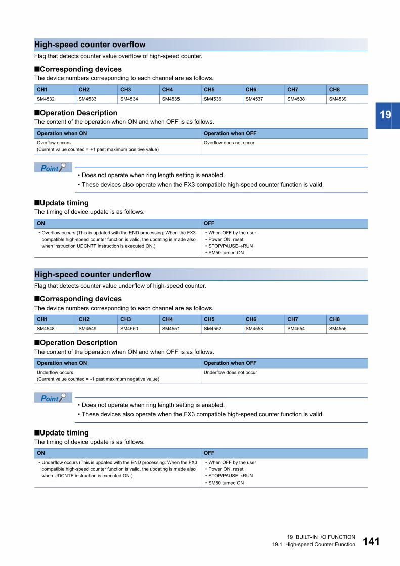
19 BUILT-IN I/O FUNCTION
19.1 High-speed Counter Function 141
19
High-speed counter overflow
Flag that detects counter value overflow of high-speed counter.
■Corresponding devicesThe device numbers corresponding to each channel are as follows.
■Operation DescriptionThe content of the operation when ON and when OFF is as follows.
� Does not operate when ring length setting is enabled.
� These devices also operate when the FX3 compatible high-speed counter function is valid.
■Update timingThe timing of device update is as follows.
High-speed counter underflow
Flag that detects counter value underflow of high-speed counter.
■Corresponding devicesThe device numbers corresponding to each channel are as follows.
■Operation DescriptionThe content of the operation when ON and when OFF is as follows.
� Does not operate when ring length setting is enabled.
� These devices also operate when the FX3 compatible high-speed counter function is valid.
■Update timingThe timing of device update is as follows.
CH1 CH2 CH3 CH4 CH5 CH6 CH7 CH8
SM4532 SM4533 SM4534 SM4535 SM4536 SM4537 SM4538 SM4539
Operation when ON Operation when OFF
Overflow occurs
(Current value counted = +1 past maximum positive value)
Overflow does not occur
ON OFF
� Overflow occurs (This is updated with the END processing. When the FX3
compatible high-speed counter function is valid, the updating is made also
when instruction UDCNTF instruction is executed ON.)
� When OFF by the user
� Power ON, reset
� STOP/PAUSERUN
� SM50 turned ON
CH1 CH2 CH3 CH4 CH5 CH6 CH7 CH8
SM4548 SM4549 SM4550 SM4551 SM4552 SM4553 SM4554 SM4555
Operation when ON Operation when OFF
Underflow occurs
(Current value counted = -1 past maximum negative value)
Underflow does not occur
ON OFF
� Underflow occurs (This is updated with the END processing. When the FX3
compatible high-speed counter function is valid, the updating is made also
when UDCNTF instruction is executed ON.)
� When OFF by the user
� Power ON, reset
� STOP/PAUSERUN
� SM50 turned ON
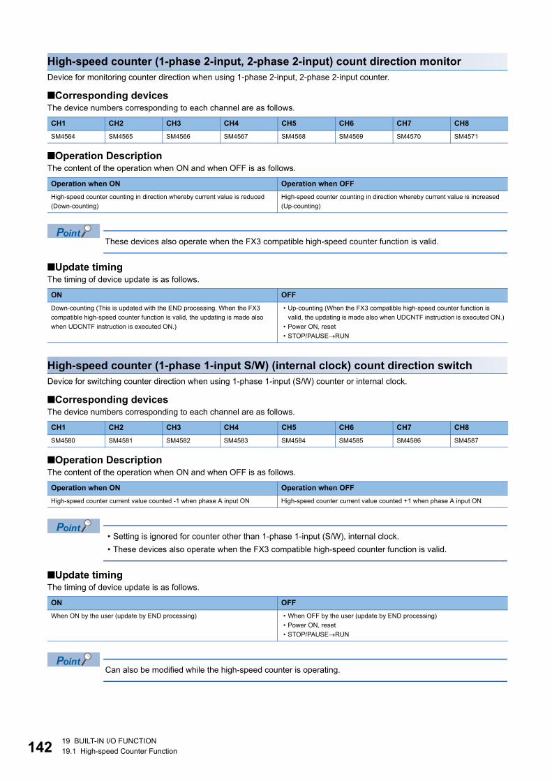
14219 BUILT-IN I/O FUNCTION
19.1 High-speed Counter Function
High-speed counter (1-phase 2-input, 2-phase 2-input) count direction monitor
Device for monitoring counter direction when using 1-phase 2-input, 2-phase 2-input counter.
■Corresponding devicesThe device numbers corresponding to each channel are as follows.
■Operation DescriptionThe content of the operation when ON and when OFF is as follows.
These devices also operate when the FX3 compatible high-speed counter function is valid.
■Update timingThe timing of device update is as follows.
High-speed counter (1-phase 1-input S/W) (internal clock) count direction switch
Device for switching counter direction when using 1-phase 1-input (S/W) counter or internal clock.
■Corresponding devicesThe device numbers corresponding to each channel are as follows.
■Operation DescriptionThe content of the operation when ON and when OFF is as follows.
� Setting is ignored for counter other than 1-phase 1-input (S/W), internal clock.
� These devices also operate when the FX3 compatible high-speed counter function is valid.
■Update timingThe timing of device update is as follows.
Can also be modified while the high-speed counter is operating.
CH1 CH2 CH3 CH4 CH5 CH6 CH7 CH8
SM4564 SM4565 SM4566 SM4567 SM4568 SM4569 SM4570 SM4571
Operation when ON Operation when OFF
High-speed counter counting in direction whereby current value is reduced
(Down-counting)
High-speed counter counting in direction whereby current value is increased
(Up-counting)
ON OFF
Down-counting (This is updated with the END processing. When the FX3
compatible high-speed counter function is valid, the updating is made also
when UDCNTF instruction is executed ON.)
� Up-counting (When the FX3 compatible high-speed counter function is
valid, the updating is made also when UDCNTF instruction is executed ON.)
� Power ON, reset
� STOP/PAUSERUN
CH1 CH2 CH3 CH4 CH5 CH6 CH7 CH8
SM4580 SM4581 SM4582 SM4583 SM4584 SM4585 SM4586 SM4587
Operation when ON Operation when OFF
High-speed counter current value counted -1 when phase A input ON High-speed counter current value counted +1 when phase A input ON
ON OFF
When ON by the user (update by END processing) � When OFF by the user (update by END processing)
� Power ON, reset
� STOP/PAUSERUN
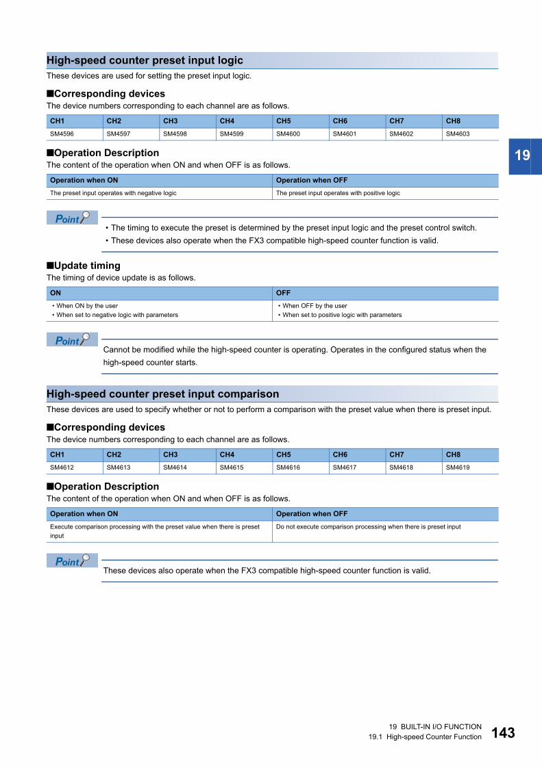
19 BUILT-IN I/O FUNCTION
19.1 High-speed Counter Function 143
19
High-speed counter preset input logic
These devices are used for setting the preset input logic.
■Corresponding devicesThe device numbers corresponding to each channel are as follows.
■Operation DescriptionThe content of the operation when ON and when OFF is as follows.
� The timing to execute the preset is determined by the preset input logic and the preset control switch.
� These devices also operate when the FX3 compatible high-speed counter function is valid.
■Update timingThe timing of device update is as follows.
Cannot be modified while the high-speed counter is operating. Operates in the configured status when the
high-speed counter starts.
High-speed counter preset input comparison
These devices are used to specify whether or not to perform a comparison with the preset value when there is preset input.
■Corresponding devicesThe device numbers corresponding to each channel are as follows.
■Operation DescriptionThe content of the operation when ON and when OFF is as follows.
These devices also operate when the FX3 compatible high-speed counter function is valid.
CH1 CH2 CH3 CH4 CH5 CH6 CH7 CH8
SM4596 SM4597 SM4598 SM4599 SM4600 SM4601 SM4602 SM4603
Operation when ON Operation when OFF
The preset input operates with negative logic The preset input operates with positive logic
ON OFF
� When ON by the user
� When set to negative logic with parameters
� When OFF by the user
� When set to positive logic with parameters
CH1 CH2 CH3 CH4 CH5 CH6 CH7 CH8
SM4612 SM4613 SM4614 SM4615 SM4616 SM4617 SM4618 SM4619
Operation when ON Operation when OFF
Execute comparison processing with the preset value when there is preset
input
Do not execute comparison processing when there is preset input
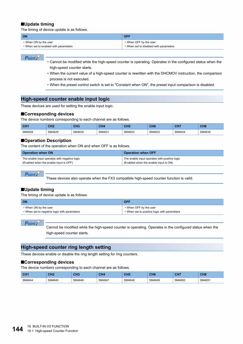
14419 BUILT-IN I/O FUNCTION
19.1 High-speed Counter Function
■Update timingThe timing of device update is as follows.
� Cannot be modified while the high-speed counter is operating. Operates in the configured status when the
high-speed counter starts.
� When the current value of a high-speed counter is rewritten with the DHCMOV instruction, the comparison
process is not executed.
� When the preset control switch is set to "Constant when ON", the preset input comparison is disabled.
High-speed counter enable input logic
These devices are used for setting the enable input logic.
■Corresponding devicesThe device numbers corresponding to each channel are as follows.
■Operation DescriptionThe content of the operation when ON and when OFF is as follows.
These devices also operate when the FX3 compatible high-speed counter function is valid.
■Update timingThe timing of device update is as follows.
Cannot be modified while the high-speed counter is operating. Operates in the configured status when the
high-speed counter starts.
High-speed counter ring length setting
These devices enable or disable the ring length setting for ring counters.
■Corresponding devicesThe device numbers corresponding to each channel are as follows.
ON OFF
� When ON by the user
� When set to enabled with parameters
� When OFF by the user
� When set to disabled with parameters
CH1 CH2 CH3 CH4 CH5 CH6 CH7 CH8
SM4628 SM4629 SM4630 SM4631 SM4632 SM4633 SM4634 SM4635
Operation when ON Operation when OFF
The enable input operates with negative logic
(Enabled when the enable input is OFF)
The enable input operates with positive logic
(Enabled when the enable input is ON)
ON OFF
� When ON by the user
� When set to negative logic with parameters
� When OFF by the user
� When set to positive logic with parameters
CH1 CH2 CH3 CH4 CH5 CH6 CH7 CH8
SM4644 SM4645 SM4646 SM4647 SM4648 SM4649 SM4650 SM4651
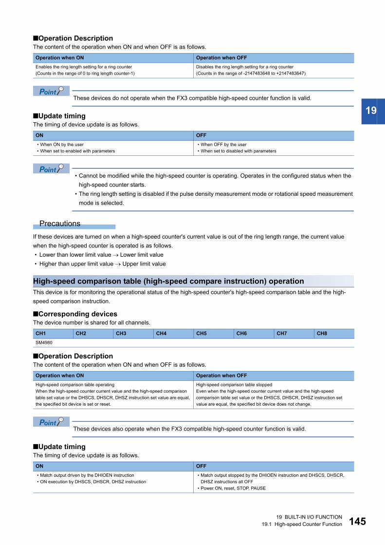
19 BUILT-IN I/O FUNCTION
19.1 High-speed Counter Function 145
19
■Operation DescriptionThe content of the operation when ON and when OFF is as follows.
These devices do not operate when the FX3 compatible high-speed counter function is valid.
■Update timingThe timing of device update is as follows.
� Cannot be modified while the high-speed counter is operating. Operates in the configured status when the
high-speed counter starts.
� The ring length setting is disabled if the pulse density measurement mode or rotational speed measurement
mode is selected.
Precautions
If these devices are turned on when a high-speed counter's current value is out of the ring length range, the current value
when the high-speed counter is operated is as follows.
� Lower than lower limit value Lower limit value
� Higher than upper limit value Upper limit value
High-speed comparison table (high-speed compare instruction) operation
This device is for monitoring the operational status of the high-speed counter's high-speed comparison table and the high-
speed comparison instruction.
■Corresponding devicesThe device number is shared for all channels.
■Operation DescriptionThe content of the operation when ON and when OFF is as follows.
These devices also operate when the FX3 compatible high-speed counter function is valid.
■Update timingThe timing of device update is as follows.
Operation when ON Operation when OFF
Enables the ring length setting for a ring counter
(Counts in the range of 0 to ring length counter-1)
Disables the ring length setting for a ring counter
(Counts in the range of -2147483648 to +2147483647)
ON OFF
� When ON by the user
� When set to enabled with parameters
� When OFF by the user
� When set to disabled with parameters
CH1 CH2 CH3 CH4 CH5 CH6 CH7 CH8
SM4980
Operation when ON Operation when OFF
High-speed comparison table operating
When the high-speed counter current value and the high-speed comparison
table set value or the DHSCS, DHSCR, DHSZ instruction set value are equal,
the specified bit device is set or reset.
High-speed comparison table stopped
Even when the high-speed counter current value and the high-speed
comparison table set value or the DHSCS, DHSCR, DHSZ instruction set
value are equal, the specified bit device does not change.
ON OFF
� Match output driven by the DHIOEN instruction
� ON execution by DHSCS, DHSCR, DHSZ instruction
� Match output stopped by the DHIOEN instruction and DHSCS, DHSCR,
DHSZ instructions all OFF
� Power ON, reset, STOP, PAUSE
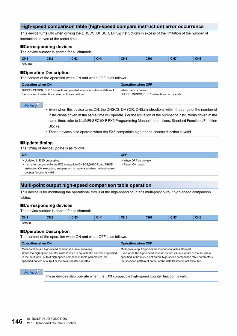
14619 BUILT-IN I/O FUNCTION
19.1 High-speed Counter Function
High-speed comparison table (high-speed compare instruction) error occurrence
This device turns ON when driving the DHSCS, DHSCR, DHSZ instructions in excess of the limitation of the number of
instructions driven at the same time.
■Corresponding devicesThe device number is shared for all channels.
■Operation DescriptionThe content of the operation when ON and when OFF is as follows.
� Even when this device turns ON, the DHSCS, DHSCR, DHSZ instructions within the range of the number of
instructions driven at the same time will operate. For the limitation of the number of instructions driven at the
same time, refer to MELSEC iQ-F FX5 Programming Manual (Instructions, Standard Functions/Function
Blocks).
� These devices also operate when the FX3 compatible high-speed counter function is valid.
■Update timingThe timing of device update is as follows.
Multi-point output high-speed comparison table operation
This device is for monitoring the operational status of the high-speed counter's multi-point output high-speed comparison
tables.
■Corresponding devicesThe device number is shared for all channels.
■Operation DescriptionThe content of the operation when ON and when OFF is as follows.
These devices also operate when the FX3 compatible high-speed counter function is valid.
CH1 CH2 CH3 CH4 CH5 CH6 CH7 CH8
SM4982
Operation when ON Operation when OFF
DHSCS, DHSCR, DHSZ instructions operated in excess of the limitation of
the number of instructions driven at the same time
When there is no error
DHSCS, DHSCR, DHSZ instructions can operate
ON OFF
� Updated in END processing
� If an error occurs while the FX3 compatible DHSCS,DHSCR,and DHSZ
instruction ON execution, an operation is made also when the high-speed
counter function is valid.
� When OFF by the user
� Power ON, reset
CH1 CH2 CH3 CH4 CH5 CH6 CH7 CH8
SM5000
Operation when ON Operation when OFF
Multi-point output high-speed comparison table operating
When the high-speed counter current value is equal to the set value specified
in the multi-point output high-speed comparison table parameters, the
specified pattern of output or the data transfer operates.
Multi-point output high-speed comparison tables stopped
Even when the high-speed counter current value is equal to the set value
specified in the multi-point output high-speed comparison table parameters,
the specified pattern of output or the data transfer is not executed.
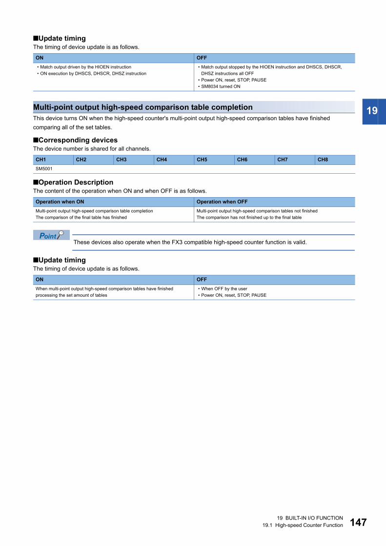
19 BUILT-IN I/O FUNCTION
19.1 High-speed Counter Function 147
19
■Update timingThe timing of device update is as follows.
Multi-point output high-speed comparison table completion
This device turns ON when the high-speed counter's multi-point output high-speed comparison tables have finished
comparing all of the set tables.
■Corresponding devicesThe device number is shared for all channels.
■Operation DescriptionThe content of the operation when ON and when OFF is as follows.
These devices also operate when the FX3 compatible high-speed counter function is valid.
■Update timingThe timing of device update is as follows.
ON OFF
� Match output driven by the HIOEN instruction
� ON execution by DHSCS, DHSCR, DHSZ instruction
� Match output stopped by the HIOEN instruction and DHSCS, DHSCR,
DHSZ instructions all OFF
� Power ON, reset, STOP, PAUSE
� SM8034 turned ON
CH1 CH2 CH3 CH4 CH5 CH6 CH7 CH8
SM5001
Operation when ON Operation when OFF
Multi-point output high-speed comparison table completion
The comparison of the final table has finished
Multi-point output high-speed comparison tables not finished
The comparison has not finished up to the final table
ON OFF
When multi-point output high-speed comparison tables have finished
processing the set amount of tables
� When OFF by the user
� Power ON, reset, STOP, PAUSE
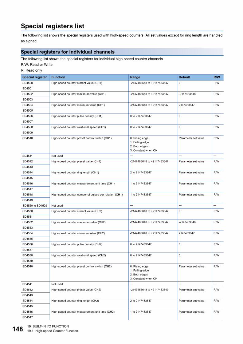
14819 BUILT-IN I/O FUNCTION
19.1 High-speed Counter Function
Special registers list
The following list shows the special registers used with high-speed counters. All set values except for ring length are handled
as signed.
Special registers for individual channels
The following list shows the special registers for individual high-speed counter channels.
R/W: Read or Write
R: Read only
Special register Function Range Default R/W
SD4500 High-speed counter current value (CH1) -2147483648 to +2147483647 0 R/W
SD4501
SD4502 High-speed counter maximum value (CH1) -2147483648 to +2147483647 -2147483648 R/W
SD4503
SD4504 High-speed counter minimum value (CH1) -2147483648 to +2147483647 2147483647 R/W
SD4505
SD4506 High-speed counter pulse density (CH1) 0 to 2147483647 0 R/W
SD4507
SD4508 High-speed counter rotational speed (CH1) 0 to 2147483647 0 R/W
SD4509
SD4510 High-speed counter preset control switch (CH1) 0: Rising edge
1: Falling edge
2: Both edges
3: Constant when ON
Parameter set value R/W
SD4511 Not used
SD4512 High-speed counter preset value (CH1) -2147483648 to +2147483647 Parameter set value R/W
SD4513
SD4514 High-speed counter ring length (CH1) 2 to 2147483647 Parameter set value R/W
SD4515
SD4516 High-speed counter measurement unit time (CH1) 1 to 2147483647 Parameter set value R/W
SD4517
SD4518 High-speed counter number of pulses per rotation (CH1) 1 to 2147483647 Parameter set value R/W
SD4519
SD4520 to SD4529 Not used
SD4530 High-speed counter current value (CH2) -2147483648 to +2147483647 0 R/W
SD4531
SD4532 High-speed counter maximum value (CH2) -2147483648 to +2147483647 -2147483648 R/W
SD4533
SD4534 High-speed counter minimum value (CH2) -2147483648 to +2147483647 2147483647 R/W
SD4535
SD4536 High-speed counter pulse density (CH2) 0 to 2147483647 0 R/W
SD4537
SD4538 High-speed counter rotational speed (CH2) 0 to 2147483647 0 R/W
SD4539
SD4540 High-speed counter preset control switch (CH2) 0: Rising edge
1: Falling edge
2: Both edges
3: Constant when ON
Parameter set value R/W
SD4541 Not used
SD4542 High-speed counter preset value (CH2) -2147483648 to +2147483647 Parameter set value R/W
SD4543
SD4544 High-speed counter ring length (CH2) 2 to 2147483647 Parameter set value R/W
SD4545
SD4546 High-speed counter measurement unit time (CH2) 1 to 2147483647 Parameter set value R/W
SD4547
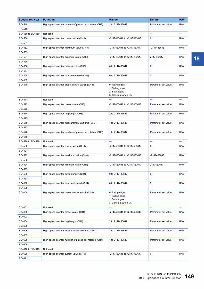
19 BUILT-IN I/O FUNCTION
19.1 High-speed Counter Function 149
19
SD4548 High-speed counter number of pulses per rotation (CH2) 1 to 2147483647 Parameter set value R/W
SD4549
SD4550 to SD4559 Not used
SD4560 High-speed counter current value (CH3) -2147483648 to +2147483647 0 R/W
SD4561
SD4562 High-speed counter maximum value (CH3) -2147483648 to +2147483647 -2147483648 R/W
SD4563
SD4564 High-speed counter minimum value (CH3) -2147483648 to +2147483647 2147483647 R/W
SD4565
SD4566 High-speed counter pulse density (CH3) 0 to 2147483647 0 R/W
SD4567
SD4568 High-speed counter rotational speed (CH3) 0 to 2147483647 0 R/W
SD4569
SD4570 High-speed counter preset control switch (CH3) 0: Rising edge
1: Falling edge
2: Both edges
3: Constant when ON
Parameter set value R/W
SD4571 Not used
SD4572 High-speed counter preset value (CH3) -2147483648 to +2147483647 Parameter set value R/W
SD4573
SD4574 High-speed counter ring length (CH3) 2 to 2147483647 Parameter set value R/W
SD4575
SD4576 High-speed counter measurement unit time (CH3) 1 to 2147483647 Parameter set value R/W
SD4577
SD4578 High-speed counter number of pulses per rotation (CH3) 1 to 2147483647 Parameter set value R/W
SD4579
SD4580 to SD4589 Not used
SD4590 High-speed counter current value (CH4) -2147483648 to +2147483647 0 R/W
SD4591
SD4592 High-speed counter maximum value (CH4) -2147483648 to +2147483647 -2147483648 R/W
SD4593
SD4594 High-speed counter minimum value (CH4) -2147483648 to +2147483647 2147483647 R/W
SD4595
SD4596 High-speed counter pulse density (CH4) 0 to 2147483647 0 R/W
SD4597
SD4598 High-speed counter rotational speed (CH4) 0 to 2147483647 0 R/W
SD4599
SD4600 High-speed counter preset control switch (CH4) 0: Rising edge
1: Falling edge
2: Both edges
3: Constant when ON
Parameter set value R/W
SD4601 Not used
SD4602 High-speed counter preset value (CH4) -2147483648 to +2147483647 Parameter set value R/W
SD4603
SD4604 High-speed counter ring length (CH4) 2 to 2147483647 Parameter set value R/W
SD4605
SD4606 High-speed counter measurement unit time (CH4) 1 to 2147483647 Parameter set value R/W
SD4607
SD4608 High-speed counter number of pulses per rotation (CH4) 1 to 2147483647 Parameter set value R/W
SD4609
SD4610 to SD4619 Not used
SD4620 High-speed counter current value (CH5) -2147483648 to +2147483647 0 R/W
SD4621
Special register Function Range Default R/W
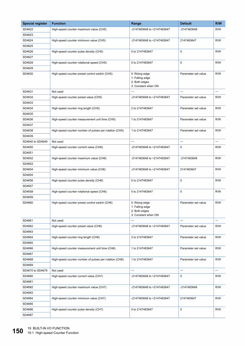
15019 BUILT-IN I/O FUNCTION
19.1 High-speed Counter Function
SD4622 High-speed counter maximum value (CH5) -2147483648 to +2147483647 -2147483648 R/W
SD4623
SD4624 High-speed counter minimum value (CH5) -2147483648 to +2147483647 2147483647 R/W
SD4625
SD4626 High-speed counter pulse density (CH5) 0 to 2147483647 0 R/W
SD4627
SD4628 High-speed counter rotational speed (CH5) 0 to 2147483647 0 R/W
SD4629
SD4630 High-speed counter preset control switch (CH5) 0: Rising edge
1: Falling edge
2: Both edges
3: Constant when ON
Parameter set value R/W
SD4631 Not used
SD4632 High-speed counter preset value (CH5) -2147483648 to +2147483647 Parameter set value R/W
SD4633
SD4634 High-speed counter ring length (CH5) 2 to 2147483647 Parameter set value R/W
SD4635
SD4636 High-speed counter measurement unit time (CH5) 1 to 2147483647 Parameter set value R/W
SD4637
SD4638 High-speed counter number of pulses per rotation (CH5) 1 to 2147483647 Parameter set value R/W
SD4639
SD4640 to SD4649 Not used
SD4650 High-speed counter current value (CH6) -2147483648 to +2147483647 0 R/W
SD4651
SD4652 High-speed counter maximum value (CH6) -2147483648 to +2147483647 -2147483648 R/W
SD4653
SD4654 High-speed counter minimum value (CH6) -2147483648 to +2147483647 2147483647 R/W
SD4655
SD4656 High-speed counter pulse density (CH6) 0 to 2147483647 0 R/W
SD4657
SD4658 High-speed counter rotational speed (CH6) 0 to 2147483647 0 R/W
SD4659
SD4660 High-speed counter preset control switch (CH6) 0: Rising edge
1: Falling edge
2: Both edges
3: Constant when ON
Parameter set value R/W
SD4661 Not used
SD4662 High-speed counter preset value (CH6) -2147483648 to +2147483647 Parameter set value R/W
SD4663
SD4664 High-speed counter ring length (CH6) 2 to 2147483647 Parameter set value R/W
SD4665
SD4666 High-speed counter measurement unit time (CH6) 1 to 2147483647 Parameter set value R/W
SD4667
SD4668 High-speed counter number of pulses per rotation (CH6) 1 to 2147483647 Parameter set value R/W
SD4669
SD4670 to SD4679 Not used
SD4680 High-speed counter current value (CH7) -2147483648 to +2147483647 0 R/W
SD4681
SD4682 High-speed counter maximum value (CH7) -2147483648 to +2147483647 -2147483648 R/W
SD4683
SD4684 High-speed counter minimum value (CH7) -2147483648 to +2147483647 2147483647 R/W
SD4685
SD4686 High-speed counter pulse density (CH7) 0 to 2147483647 0 R/W
SD4687
Special register Function Range Default R/W
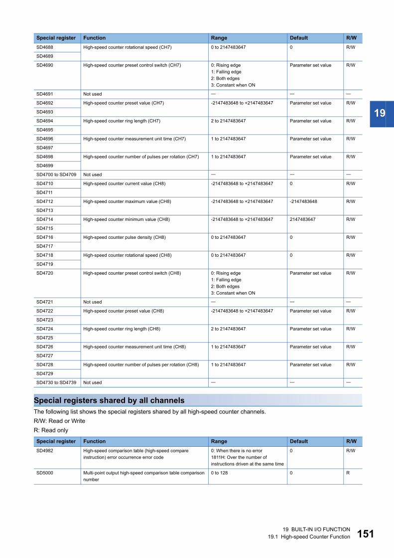
19 BUILT-IN I/O FUNCTION
19.1 High-speed Counter Function 151
19
Special registers shared by all channels
The following list shows the special registers shared by all high-speed counter channels.
R/W: Read or Write
R: Read only
SD4688 High-speed counter rotational speed (CH7) 0 to 2147483647 0 R/W
SD4689
SD4690 High-speed counter preset control switch (CH7) 0: Rising edge
1: Falling edge
2: Both edges
3: Constant when ON
Parameter set value R/W
SD4691 Not used
SD4692 High-speed counter preset value (CH7) -2147483648 to +2147483647 Parameter set value R/W
SD4693
SD4694 High-speed counter ring length (CH7) 2 to 2147483647 Parameter set value R/W
SD4695
SD4696 High-speed counter measurement unit time (CH7) 1 to 2147483647 Parameter set value R/W
SD4697
SD4698 High-speed counter number of pulses per rotation (CH7) 1 to 2147483647 Parameter set value R/W
SD4699
SD4700 to SD4709 Not used
SD4710 High-speed counter current value (CH8) -2147483648 to +2147483647 0 R/W
SD4711
SD4712 High-speed counter maximum value (CH8) -2147483648 to +2147483647 -2147483648 R/W
SD4713
SD4714 High-speed counter minimum value (CH8) -2147483648 to +2147483647 2147483647 R/W
SD4715
SD4716 High-speed counter pulse density (CH8) 0 to 2147483647 0 R/W
SD4717
SD4718 High-speed counter rotational speed (CH8) 0 to 2147483647 0 R/W
SD4719
SD4720 High-speed counter preset control switch (CH8) 0: Rising edge
1: Falling edge
2: Both edges
3: Constant when ON
Parameter set value R/W
SD4721 Not used
SD4722 High-speed counter preset value (CH8) -2147483648 to +2147483647 Parameter set value R/W
SD4723
SD4724 High-speed counter ring length (CH8) 2 to 2147483647 Parameter set value R/W
SD4725
SD4726 High-speed counter measurement unit time (CH8) 1 to 2147483647 Parameter set value R/W
SD4727
SD4728 High-speed counter number of pulses per rotation (CH8) 1 to 2147483647 Parameter set value R/W
SD4729
SD4730 to SD4739 Not used
Special register Function Range Default R/W
SD4982 High-speed comparison table (high-speed compare
instruction) error occurrence error code
0: When there is no error
1811H: Over the number of
instructions driven at the same time
0 R/W
SD5000 Multi-point output high-speed comparison table comparison
number
0 to 128 0 R
Special register Function Range Default R/W
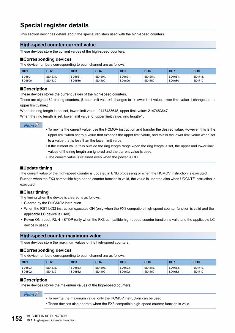
15219 BUILT-IN I/O FUNCTION
19.1 High-speed Counter Function
Special register details
This section describes details about the special registers used with the high-speed counters.
High-speed counter current value
These devices store the current values of the high-speed counters.
■Corresponding devicesThe device numbers corresponding to each channel are as follows.
■DescriptionThese devices stores the current values of the high-speed counters.
These are signed 32-bit ring counters. (Upper limit value+1 changes to lower limit value, lower limit value-1 changes to
upper limit value.)
When the ring length is not set, lower limit value: -2147483648, upper limit value: 2147483647.
When the ring length is set, lower limit value: 0, upper limit value: ring length-1.
� To rewrite the current value, use the HCMOV instruction and transfer the desired value. However, this is the
upper limit when set to a value that exceeds the upper limit value, and this is the lower limit value when set
to a value that is less than the lower limit value.
� If the current value falls outside the ring length range when the ring length is set, the upper and lower limit
values of the ring length are ignored and the current value is used.
� The current value is retained even when the power is OFF.
■Update timingThe current value of the high-speed counter is updated in END processing or when the HCMOV instruction is executed.
Further, when the FX3 compatible high-speed counter function is valid, the value is updated also when UDCNTF instruction is
executed.
■Clear timingThe timing when the device is cleared is as follows.
� Cleared by the DHCMOV instruction
� When the RST LC instruction executes ON (only when the FX3 compatible high-speed counter function is valid and the
applicable LC device is used)
� Power ON, reset, RUN→STOP (only when the FX3 compatible high-speed counter function is valid and the applicable LC
device is used)
High-speed counter maximum value
These devices store the maximum values of the high-speed counters.
■Corresponding devicesThe device numbers corresponding to each channel are as follows.
■DescriptionThese devices stores the maximum values of the high-speed counters.
� To rewrite the maximum value, only the HCMOV instruction can be used.
� These devices also operate when the FX3 compatible high-speed counter function is valid.
CH1 CH2 CH3 CH4 CH5 CH6 CH7 CH8
SD4501,
SD4500
SD4531,
SD4530
SD4561,
SD4560
SD4591,
SD4590
SD4621,
SD4620
SD4651,
SD4650
SD4681,
SD4680
SD4711,
SD4710
CH1 CH2 CH3 CH4 CH5 CH6 CH7 CH8
SD4503,
SD4502
SD4533,
SD4532
SD4563,
SD4562
SD4593,
SD4592
SD4623,
SD4622
SD4653,
SD4652
SD4683,
SD4682
SD4713,
SD4712
19 BUILT-IN I/O FUNCTION
19.1 High-speed Counter Function 153
19
■Update timingWhen the current value of a high-speed counter exceeds the maximum value, the value is updated in END processing. When
the value is read using the HCMOV instruction, it is first updated to the latest value and then read. Further, when the FX3
compatible high-speed counter function is valid, the value is updated also when UDCNTF instruction is executed.
■Clear timingThe timing when the device is cleared is as follows.
� Power ON, Reset
High-speed counter minimum value
These devices store the minimum values of the high-speed counters.
■Corresponding devicesThe device numbers corresponding to each channel are as follows.
■DescriptionThese devices stores the minimum values of the high-speed counters.
� To rewrite the minimum value, only the HCMOV instruction can be used.
� These devices also operate when the FX3 compatible high-speed counter function is valid.
■Update timingWhen the current value of a high-speed counter becomes less than the minimum value, the value is updated in END
processing. When the value is read using the HCMOV instruction, it is first updated to the latest value and then read. Further,
when the FX3 compatible high-speed counter function is valid, the value is updated also when UDCNTF instruction is
executed.
■Clear timingThe timing when the device is cleared is as follows.
� Power ON, Reset
High-speed counter pulse density
These devices store the measurement results of pulse density measurement mode.
■Corresponding devicesThe device numbers corresponding to each channel are as follows.
■DescriptionThese devices store the measurement results of pulse density measurement mode (rotational speed measurement mode).
� These devices also store the pulse density measurement when in rotational speed measurement mode.
� If the FX3 compatible high-speed counter function is valid, these devices operate only when the SPD
instruction operates.
■Update timingThe pulse density is updated at each measurement unit time when set to pulse density measurement mode (rotational speed
measurement mode) with parameters.
■Clear timingThe timing when the device is cleared is as follows.
CH1 CH2 CH3 CH4 CH5 CH6 CH7 CH8
SD4505,
SD4504
SD4535,
SD4534
SD4565,
SD4564
SD4595,
SD4594
SD4625,
SD4624
SD4655,
SD4654
SD4685,
SD4684
SD4715,
SD4714
CH1 CH2 CH3 CH4 CH5 CH6 CH7 CH8
SD4507,
SD4506
SD4537,
SD4536
SD4567,
SD4566
SD4597,
SD4596
SD4627,
SD4626
SD4657,
SD4656
SD4687,
SD4686
SD4717,
SD4716
15419 BUILT-IN I/O FUNCTION
19.1 High-speed Counter Function
� Power ON, Reset, STOP/PAUSERUN
High-speed counter rotational speed
These devices store the measurement results of rotational speed measurement mode.
■Corresponding devicesThe device numbers corresponding to each channel are as follows.
■DescriptionThese devices store the measurement results of rotational speed measurement mode.
� These devices also store the rotational speed when in pulse density measurement mode.
� These devices do not operate when the FX3 compatible high-speed counter function is valid.
■Update timingThe rotational speed is updated at each measurement unit time when set to rotational speed measurement mode with
parameters.
■Clear timingThe timing when the device is cleared is as follows.
� Power ON, Reset, STOP/PAUSERUN
High-speed counter preset control switch
These devices set the preset input operation of the high-speed counters.
■Corresponding devicesThe device numbers corresponding to each channel are as follows.
■DescriptionThese devices set the timing to execute preset input. The table below shows the operations of the setting values.
*1 When the preset control switch is set to "3: Constant when ON", the preset input comparison cannot be used even if the parameter of
the preset input comparison (special relay) is enabled.
� While the high-speed counter is operating, the value is not reflected even if modified. It operates in the
status when the high-speed counter starts.
� These devices also operate when the FX3 compatible high-speed counter function is valid.
■Clear timingThe timing when the device is cleared is as follows.
� Power ON, Reset, STOPRUN
CH1 CH2 CH3 CH4 CH5 CH6 CH7 CH8
SD4509,
SD4508
SD4539,
SD4538
SD4569,
SD4568
SD4599,
SD4598
SD4629,
SD4628
SD4659,
SD4658
SD4689,
SD4688
SD4719,
SD4718
CH1 CH2 CH3 CH4 CH5 CH6 CH7 CH8
SD4510 SD4540 SD4570 SD4600 SD4630 SD4660 SD4690 SD4720
Setting value Description
0 Executes the preset on the rising edge.
1 Executes the preset on the falling edge.
2 Executes the preset on both edges.
3 Constantly executes the preset when ON.*1
Other than above Operates as the rising edge.
Executes the preset on the rising edge.
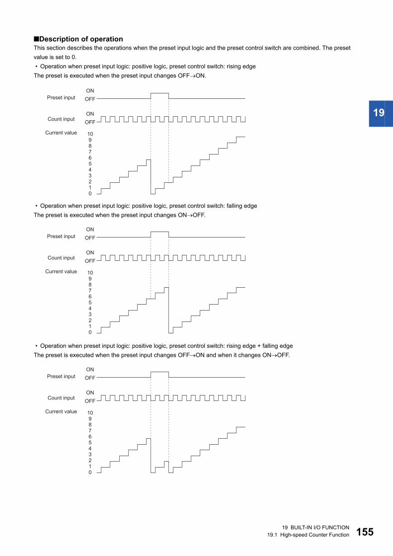
19 BUILT-IN I/O FUNCTION
19.1 High-speed Counter Function 155
19
■Description of operationThis section describes the operations when the preset input logic and the preset control switch are combined. The preset
value is set to 0.
� Operation when preset input logic: positive logic, preset control switch: rising edge
The preset is executed when the preset input changes OFFON.
� Operation when preset input logic: positive logic, preset control switch: falling edge
The preset is executed when the preset input changes ONOFF.
� Operation when preset input logic: positive logic, preset control switch: rising edge + falling edge
The preset is executed when the preset input changes OFFON and when it changes ONOFF.
Preset input
Count inputON
OFF
ON
OFF
Current value 109876543210
Preset input
Count inputON
OFF
ON
OFF
Current value 109876543210
Preset input
Count inputON
OFF
ON
OFF
Current value 109876543210
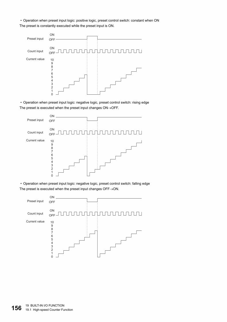
15619 BUILT-IN I/O FUNCTION
19.1 High-speed Counter Function
� Operation when preset input logic: positive logic, preset control switch: constant when ON
The preset is constantly executed while the preset input is ON.
� Operation when preset input logic: negative logic, preset control switch: rising edge
The preset is executed when the preset input changes ONOFF.
� Operation when preset input logic: negative logic, preset control switch: falling edge
The preset is executed when the preset input changes OFFON.
Preset input
Count inputON
OFF
ON
OFF
Current value 109876543210
Preset input
Count inputON
OFF
ON
OFF
Current value 109876543210
Preset input
Count inputON
OFF
ON
OFF
Current value 109876543210
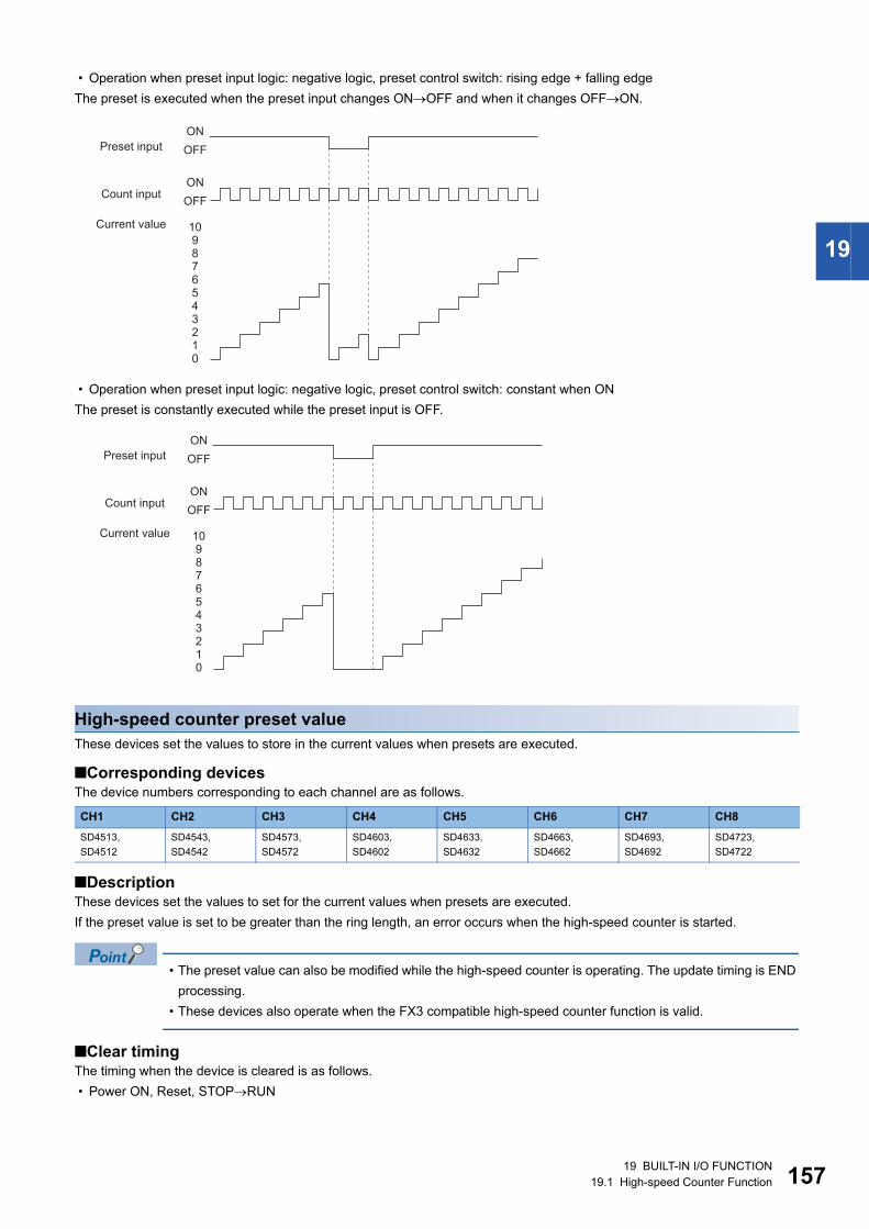
19 BUILT-IN I/O FUNCTION
19.1 High-speed Counter Function 157
19
� Operation when preset input logic: negative logic, preset control switch: rising edge + falling edge
The preset is executed when the preset input changes ONOFF and when it changes OFFON.
� Operation when preset input logic: negative logic, preset control switch: constant when ON
The preset is constantly executed while the preset input is OFF.
High-speed counter preset value
These devices set the values to store in the current values when presets are executed.
■Corresponding devicesThe device numbers corresponding to each channel are as follows.
■DescriptionThese devices set the values to set for the current values when presets are executed.
If the preset value is set to be greater than the ring length, an error occurs when the high-speed counter is started.
� The preset value can also be modified while the high-speed counter is operating. The update timing is END
processing.
� These devices also operate when the FX3 compatible high-speed counter function is valid.
■Clear timingThe timing when the device is cleared is as follows.
� Power ON, Reset, STOPRUN
CH1 CH2 CH3 CH4 CH5 CH6 CH7 CH8
SD4513,
SD4512
SD4543,
SD4542
SD4573,
SD4572
SD4603,
SD4602
SD4633,
SD4632
SD4663,
SD4662
SD4693,
SD4692
SD4723,
SD4722
Preset input
Count inputON
OFF
ON
OFF
Current value 109876543210
Preset input
Count inputON
OFF
ON
OFF
Current value 109876543210
15819 BUILT-IN I/O FUNCTION
19.1 High-speed Counter Function
High-speed counter ring length
These devices set the ring length of the high-speed counters.
■Corresponding devicesThe device numbers corresponding to each channel are as follows.
■DescriptionThese devices set the ring length of the high-speed counters.
These set values are valid when the ring length setting is set to enabled.
� While the high-speed counter is operating, the value is not reflected even if modified. It operates in the
status when the high-speed counter starts.
� These devices do not operate when the FX3 compatible high-speed counter function is valid.
■Clear timingThe timing when the device is cleared is as follows.
� Power ON, Reset, STOPRUN
Precautions
If the ring length is set to less than the lower limit value or more than the upper limit value, the ring length operates at the lower
limit value or the upper limit value. However, the set value is stored as is.
High-speed counter measurement unit time
These devices set the measurement unit of pulse density measurement mode.
■Corresponding devicesThe device numbers corresponding to each channel are as follows.
■DescriptionThese devices set the time to measure pulse density (rotational speed) in 1 ms units when high-speed counters are operating
in pulse density measurement mode.
� If the value is modified while the high-speed counter is operating, the rewritten value is reflected after the
measurement before the value was modified is finished.
� If the FX3 compatible high-speed counter function is valid, these devices operate only when the SPD
instruction operates. The value in the operand of the SPD instruction is written.
■Clear timingThe timing when the device is cleared is as follows.
� Power ON, Reset, STOPRUN
Precautions
If the set value for the measurement unit time is set to less than the lower limit value or more than the upper limit value, the
measurement unit time operates at the lower limit value or the upper limit value. However, the set value is stored as is.
CH1 CH2 CH3 CH4 CH5 CH6 CH7 CH8
SD4515,
SD4514
SD4545,
SD4544
SD4575,
SD4574
SD4605,
SD4604
SD4635,
SD4634
SD4665,
SD4664
SD4695,
SD4694
SD4725,
SD4724
CH1 CH2 CH3 CH4 CH5 CH6 CH7 CH8
SD4517,
SD4516
SD4547,
SD4546
SD4577,
SD4576
SD4607,
SD4606
SD4637,
SD4636
SD4667,
SD4666
SD4697,
SD4696
SD4727,
SD4726
19 BUILT-IN I/O FUNCTION
19.1 High-speed Counter Function 159
19
High-speed counter number of pulses per rotation
These devices set the number of pulses per rotation for rotational speed measurement mode.
■Corresponding devicesThe device numbers corresponding to each channel are as follows.
■DescriptionThese devices set the number of pulses per rotation when a high-speed counter operates in rotational speed measurement
mode. The rotational speed is measured with the set value.
� If the value is modified while the high-speed counter is operating, the rewritten value is reflected after the
measurement before the value was modified is finished.
� These devices do not operate when the FX3 compatible high-speed counter function is valid.
■Clear timingThe timing when the device is cleared is as follows.
� Power ON, Reset, STOPRUN
Precautions
If the set value for the number of pulses per rotation is set to less than the lower limit value or more than the upper limit value,
the number of pulses per rotation operates at the lower limit value or the upper limit value. However, the set value is stored as
is.
High-speed comparison table (high-speed compare instruction) error occurrence error code
This device stores the high-speed comparison table, high-speed comparison instruction error.
■Corresponding devicesThe device number is shared for all channels.
■DescriptionThis device stores the error code when an error occurs in the high-speed comparison table, high-speed comparison
instruction.
These devices also operate when the FX3 compatible high-speed counter function is valid.
■Clear timingThe timing when the device is cleared is as follows.
� Power ON, Reset, SM50 turned ON
■Error codeOver the upper limit of the number of instructions driven at the same time: 1811H
CH1 CH2 CH3 CH4 CH5 CH6 CH7 CH8
SD4519,
SD4518
SD4549,
SD4548
SD4579,
SD4578
SD4609,
SD4608
SD4639,
SD4638
SD4669,
SD4668
SD4699,
SD4698
SD4729,
SD4728
CH1 CH2 CH3 CH4 CH5 CH6 CH7 CH8
SD4982
16019 BUILT-IN I/O FUNCTION
19.1 High-speed Counter Function
Multi-point output high-speed comparison table comparison number
This device stores the number of the table currently being compared in the multi-point output high-speed comparison tables.
■Corresponding devicesThe device number is shared for all channels.
■DescriptionThis device stores the number of the table currently being compared in the multi-point output high-speed comparison tables. If
0, the multi-point output high-speed comparison tables have stopped.
� When rewriting the comparison value or output data for the multi-point output high-speed comparison
tables, the table numbers from the table numbers that follow after the next table number of the table being
compared can be rewritten.
� The table number being compared and the next table number after that can be rewritten, but they will not be
compared.
� These devices also operate when the FX3 compatible high-speed counter function is valid.
■Clear timingThe timing when the device is cleared is as follows.
� Power ON, Reset, STOPRUN
CH1 CH2 CH3 CH4 CH5 CH6 CH7 CH8
SD5000
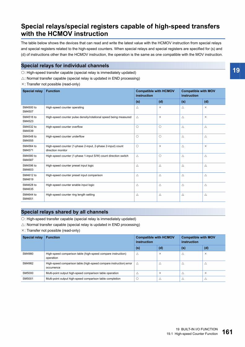
19 BUILT-IN I/O FUNCTION
19.1 High-speed Counter Function 161
19
Special relays/special registers capable of high-speed transfers with the HCMOV instruction
The table below shows the devices that can read and write the latest value with the HCMOV instruction from special relays
and special registers related to the high-speed counters. When special relays and special registers are specified for (s) and
(d) of instructions other than the HCMOV instruction, the operation is the same as one compatible with the MOV instruction.
Special relays for individual channels
: High-speed transfer capable (special relay is immediately updated)
: Normal transfer capable (special relay is updated in END processing)
: Transfer not possible (read-only)
Special relays shared by all channels
: High-speed transfer capable (special relay is immediately updated)
: Normal transfer capable (special relay is updated in END processing)
: Transfer not possible (read-only)
Special relay Function Compatible with HCMOV
instruction
Compatible with MOV
instruction
(s) (d) (s) (d)
SM4500 to
SM4507
High-speed counter operating
SM4516 to
SM4523
High-speed counter pulse density/rotational speed being measured
SM4532 to
SM4539
High-speed counter overflow
SM4548 to
SM4555
High-speed counter underflow
SM4564 to
SM4571
High-speed counter (1-phase 2-input, 2-phase 2-input) count
direction monitor
SM4580 to
SM4587
High-speed counter (1-phase 1-input S/W) count direction switch
SM4596 to
SM4603
High-speed counter preset input logic
SM4612 to
SM4619
High-speed counter preset input comparison
SM4628 to
SM4635
High-speed counter enable input logic
SM4644 to
SM4651
High-speed counter ring length setting
Special relay Function Compatible with HCMOV
instruction
Compatible with MOV
instruction
(s) (d) (s) (d)
SM4980 High-speed comparison table (high-speed compare instruction)
operation
SM4982 High-speed comparison table (high-speed compare instruction) error
occurrence
SM5000 Multi-point output high-speed comparison table operation
SM5001 Multi-point output high-speed comparison table completion
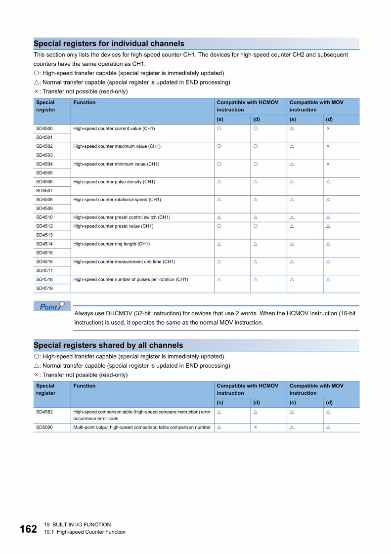
16219 BUILT-IN I/O FUNCTION
19.1 High-speed Counter Function
Special registers for individual channels
This section only lists the devices for high-speed counter CH1. The devices for high-speed counter CH2 and subsequent
counters have the same operation as CH1.
: High-speed transfer capable (special register is immediately updated)
: Normal transfer capable (special register is updated in END processing)
: Transfer not possible (read-only)
Always use DHCMOV (32-bit instruction) for devices that use 2 words. When the HCMOV instruction (16-bit
instruction) is used, it operates the same as the normal MOV instruction.
Special registers shared by all channels
: High-speed transfer capable (special register is immediately updated)
: Normal transfer capable (special register is updated in END processing)
: Transfer not possible (read-only)
Special
register
Function Compatible with HCMOV
instruction
Compatible with MOV
instruction
(s) (d) (s) (d)
SD4500 High-speed counter current value (CH1)
SD4501
SD4502 High-speed counter maximum value (CH1)
SD4503
SD4504 High-speed counter minimum value (CH1)
SD4505
SD4506 High-speed counter pulse density (CH1)
SD4507
SD4508 High-speed counter rotational speed (CH1)
SD4509
SD4510 High-speed counter preset control switch (CH1)
SD4512 High-speed counter preset value (CH1)
SD4513
SD4514 High-speed counter ring length (CH1)
SD4515
SD4516 High-speed counter measurement unit time (CH1)
SD4517
SD4518 High-speed counter number of pulses per rotation (CH1)
SD4519
Special
register
Function Compatible with HCMOV
instruction
Compatible with MOV
instruction
(s) (d) (s) (d)
SD4982 High-speed comparison table (high-speed compare instruction) error
occurrence error code
SD5000 Multi-point output high-speed comparison table comparison number
19 BUILT-IN I/O FUNCTION
19.1 High-speed Counter Function 163
19
Precautions when using high-speed counters
This section describes the precautions when using high-speed counters.
Common precautions when using high-speed counter instructions and parameters
This section describes the common precautions when using high-speed comparison tables and multi-point output comparison
tables with the high-speed counter instructions (DHSCS, DHSCR, DHSZ instructions) or parameters. For the individual
precautions on high-speed counter instructions, refer to MELSEC iQ-F FX5 Programming Manual (Instructions, Standard
Functions/Function Blocks).
■High-speed counter devicesThe current values for high-speed counters are checked with special registers for each channel.
To start or stop counting of the high-speed counters, use the HIOEN instruction or the SPD instruction.
� High-speed counter start/stop conditions
*1 Can be stopped when counting was started with the SPD instruction.
*2 Can be stopped when the high-speed comparison table is not set with parameters.
■Precautions for the counting operation when the current value is changedFor the high-speed counter instructions, high-speed comparison tables, and multi-point output high-speed comparison tables,
comparison processing is performed when the current value of the high-speed counter has changed due to pulse input. When
the preset input comparison function is also enabled, comparison processing is also performed when the preset is executed.
However, please note that the comparison processing is not performed when the current value of the high-speed counter is
changed with the following methods.
� When the current value of a high-speed counter was rewritten with the HCMOV instruction.
� When the current value of the high-speed counter is reset with the RST instruction or the ZRST instruction (when the FX3
compatible high-speed counter function is valid)
� When the current value of the high-speed counter was changed by a self-reset. (When the preset input comparison function
is disabled)
� When high-speed counter current value is the ON or OFF output result of the comparison of the DHSCS, DHSCR, DHSZ
instructions.
� When high-speed counter current value is the ON or OFF output result of the comparison of a high-speed comparison
table.
■Preset input comparison operationWhen the preset input comparison is enabled and preset control switching is set to constant when ON, the preset input
comparison does not operate.
■Timing at which the instruction is enabledThe DHSCS, DHSCR, DHSZ instructions are enabled at the END instruction for the scan in which the instructions are driven.
Even when the comparison value is changed, it is updated at the END instruction for the scan in which it was changed .
■Configuring high-speed comparison tables with parametersOperations of DHSCS, DHSCR, DHSZ instructions of the same comparison value are executed after high-speed comparison
tables set with parameters. The high-speed comparison table is processed sequentially from the top of the table.
Function Start Stop
Counting � HIOEN instruction
� SPD instruction
� HIOEN instruction
� SPD instruction*1
Comparison processing � HIOEN instruction
� DHSCS, DHSCR, DHSZ instructions
� HIOEN instruction
� DHSCS, DHSCR, DHSZ instructions*2
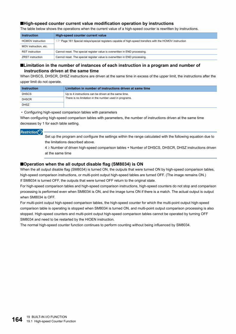
16419 BUILT-IN I/O FUNCTION
19.1 High-speed Counter Function
■High-speed counter current value modification operation by instructionsThe table below shows the operations when the current value of a high-speed counter is rewritten by instructions.
■Limitation in the number of instances of each instruction in a program and number of
instructions driven at the same timeWhen DHSCS, DHSCR, DHSZ instructions are driven at the same time in excess of the upper limit, the instructions after the
upper limit do not operate.
� Configuring high-speed comparison tables with parameters
When configuring high-speed comparison tables with parameters, the number of instructions driven at the same time
decreases by 1 for each table setting.
Set up the program and configure the settings within the range calculated with the following equation due to
the limitations described above.
4 Number of driven high-speed comparison tables + Number of DHSCS, DHSCR, DHSZ instructions driven
at the same time
■Operation when the all output disable flag (SM8034) is ONWhen the all output disable flag (SM8034) is turned ON, the outputs that were turned ON by high-speed comparison tables,
high-speed comparison instructions, or multi-point output high-speed tables are turned OFF. (The image remains ON.)
If SM8034 is turned OFF, the outputs that were turned OFF return to the original state.
For high-speed comparison tables and high-speed comparison instructions, high-speed counters do not stop and comparison
processing is performed even when SM8034 is ON, and the image turns ON if there is a match. The actual output is output
when SM8034 is OFF.
For multi-point output high-speed comparison tables, the high-speed counter for which the multi-point output high-speed
comparison table is operating is stopped when SM8034 is turned ON, and multi-point output comparison processing is also
stopped. High-speed counters and multi-point output high-speed comparison tables cannot be operated by turning OFF
SM8034 and need to be restarted by the HIOEN instruction.
The normal high-speed counter function continues to perform counting without being influenced by SM8034.
Instruction High-speed counter current value
HCMOV instruction Page 161 Special relays/special registers capable of high-speed transfers with the HCMOV instruction
MOV instruction, etc.
RST instruction Cannot reset. The special register value is overwritten in END processing.
ZRST instruction Cannot reset. The special register value is overwritten in END processing.
Instruction Limitation in number of instructions driven at same time
DHSCS Up to 4 instructions can be driven at the same time.
There is no limitation in the number used in programs.DHSCR
DHSZ
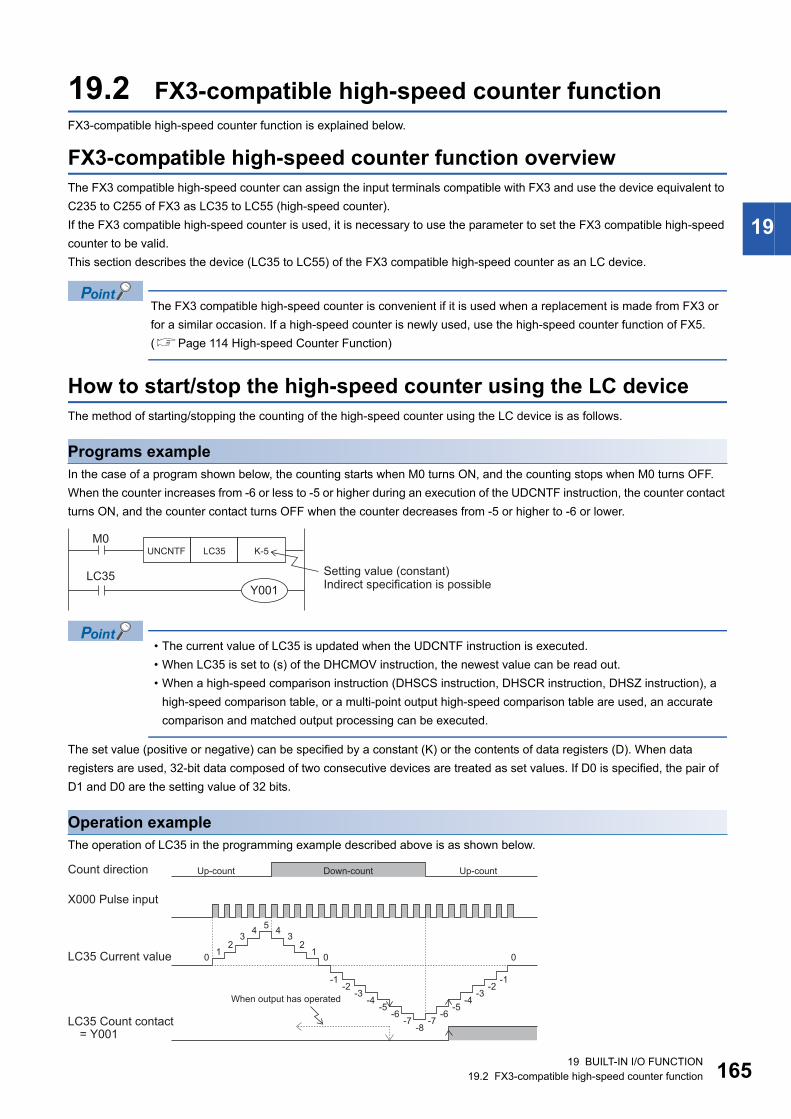
19 BUILT-IN I/O FUNCTION
19.2 FX3-compatible high-speed counter function 165
19
19.2 FX3-compatible high-speed counter function
FX3-compatible high-speed counter function is explained below.
FX3-compatible high-speed counter function overview
The FX3 compatible high-speed counter can assign the input terminals compatible with FX3 and use the device equivalent to
C235 to C255 of FX3 as LC35 to LC55 (high-speed counter).
If the FX3 compatible high-speed counter is used, it is necessary to use the parameter to set the FX3 compatible high-speed
counter to be valid.
This section describes the device (LC35 to LC55) of the FX3 compatible high-speed counter as an LC device.
The FX3 compatible high-speed counter is convenient if it is used when a replacement is made from FX3 or
for a similar occasion. If a high-speed counter is newly used, use the high-speed counter function of FX5.
(Page 114 High-speed Counter Function)
How to start/stop the high-speed counter using the LC device
The method of starting/stopping the counting of the high-speed counter using the LC device is as follows.
Programs example
In the case of a program shown below, the counting starts when M0 turns ON, and the counting stops when M0 turns OFF.
When the counter increases from -6 or less to -5 or higher during an execution of the UDCNTF instruction, the counter contact
turns ON, and the counter contact turns OFF when the counter decreases from -5 or higher to -6 or lower.
� The current value of LC35 is updated when the UDCNTF instruction is executed.
� When LC35 is set to (s) of the DHCMOV instruction, the newest value can be read out.
� When a high-speed comparison instruction (DHSCS instruction, DHSCR instruction, DHSZ instruction), a
high-speed comparison table, or a multi-point output high-speed comparison table are used, an accurate
comparison and matched output processing can be executed.
The set value (positive or negative) can be specified by a constant (K) or the contents of data registers (D). When data
registers are used, 32-bit data composed of two consecutive devices are treated as set values. If D0 is specified, the pair of
D1 and D0 are the setting value of 32 bits.
Operation example
The operation of LC35 in the programming example described above is as shown below.
M0
LC35 Setting value (constant)Indirect specification is possible
Y001
UNCNTF LC35 K-5
Count direction Up-count Up-countDown-count
0 0 0
-1 -1-2 -2
-3 -3-4 -4
-5 -5-6 -6
-7 -7-8
1 12 2
3 34 4
5
X000 Pulse input
LC35 Current value
LC35 Count contact= Y001
When output has operated
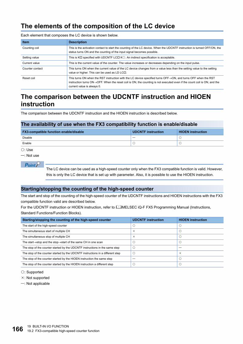
16619 BUILT-IN I/O FUNCTION
19.2 FX3-compatible high-speed counter function
The elements of the composition of the LC device
Each element that composes the LC device is shown below.
The comparison between the UDCNTF instruction and HIOEN instruction
The comparison between the UDCNTF instruction and the HIOEN instruction is described below.
The availability of use when the FX3 compatibility function is enable/disable
: Use
: Not use
The LC device can be used as a high-speed counter only when the FX3 compatible function is valid. However,
this is only the LC device that is set up with parameter. Also, it is possible to use the HIOEN instruction.
Starting/stopping the counting of the high-speed counter
The start and stop of the counting of the high-speed counter of the UDCNTF instructions and HIOEN instructions with the FX3
compatible function valid are described below.
For the UDCNTF instruction or HIOEN instruction, refer to MELSEC iQ-F FX5 Programming Manual (Instructions,
Standard Functions/Function Blocks).
: Supported
: Not supported
: Not applicable
Item Description
Counting coil This is the activation contact to start the counting of the LC device. When the UDCNTF instruction is turned OFF/ON, the
status turns ON and the counting of the input signal becomes possible.
Setting value This is K specified with UDCNTF LC K. An indirect specification is acceptable.
Current value This is the current value of the counter. The value increases or decreases depending on the input pulse.
Counter contact This turns ON when the current value of the LC device changes from a value less than the setting value to the setting
value or higher. This can be used as LD LC.
Reset coil This turns ON when the RST instruction with the LC device specified turns OFFON, and turns OFF when the RST
instruction turns ONOFF. When the reset coil is ON, the counting is not executed even if the count coil is ON, and the
current value is always 0.
FX3-compatible function enable/disable UDCNTF instruction HIOEN instruction
Disable
Enable
Starting/stopping the counting of the high-speed counter UDCNTF instruction HIOEN instruction
The start of the high-speed counter
The simultaneous start of multiple CH
The simultaneous stop of multiple CH
The startstop and the stopstart of the same CH in one scan
The stop of the counter started by the UDCNTF instructions in the same step
The stop of the counter started by the UDCNTF instructions in a different step
The stop of the counter started by the HIOEN instruction the same step
The stop of the counter started by the HIOEN instruction a different step
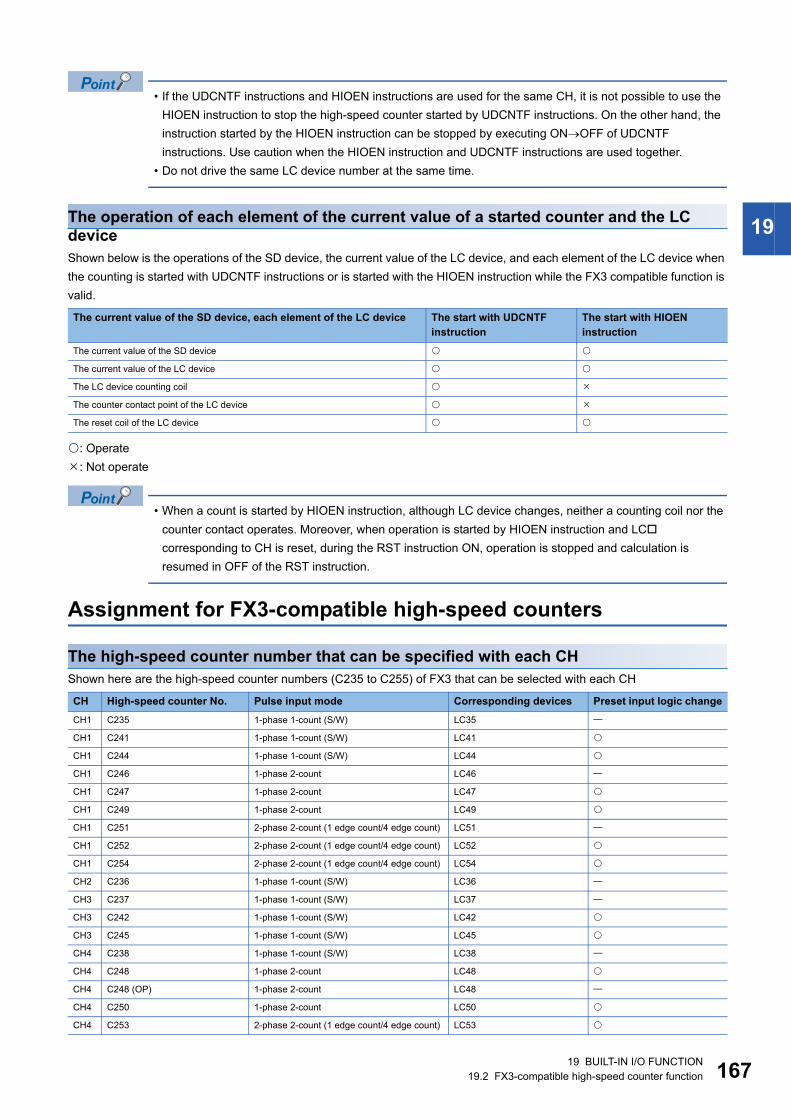
19 BUILT-IN I/O FUNCTION
19.2 FX3-compatible high-speed counter function 167
19
� If the UDCNTF instructions and HIOEN instructions are used for the same CH, it is not possible to use the
HIOEN instruction to stop the high-speed counter started by UDCNTF instructions. On the other hand, the
instruction started by the HIOEN instruction can be stopped by executing ONOFF of UDCNTF
instructions. Use caution when the HIOEN instruction and UDCNTF instructions are used together.
� Do not drive the same LC device number at the same time.
The operation of each element of the current value of a started counter and the LC device
Shown below is the operations of the SD device, the current value of the LC device, and each element of the LC device when
the counting is started with UDCNTF instructions or is started with the HIOEN instruction while the FX3 compatible function is
valid.
: Operate
: Not operate
� When a count is started by HIOEN instruction, although LC device changes, neither a counting coil nor the
counter contact operates. Moreover, when operation is started by HIOEN instruction and LC
corresponding to CH is reset, during the RST instruction ON, operation is stopped and calculation is
resumed in OFF of the RST instruction.
Assignment for FX3-compatible high-speed counters
The high-speed counter number that can be specified with each CH
Shown here are the high-speed counter numbers (C235 to C255) of FX3 that can be selected with each CH
The current value of the SD device, each element of the LC device The start with UDCNTF
instruction
The start with HIOEN
instruction
The current value of the SD device
The current value of the LC device
The LC device counting coil
The counter contact point of the LC device
The reset coil of the LC device
CH High-speed counter No. Pulse input mode Corresponding devices Preset input logic change
CH1 C235 1-phase 1-count (S/W) LC35
CH1 C241 1-phase 1-count (S/W) LC41
CH1 C244 1-phase 1-count (S/W) LC44
CH1 C246 1-phase 2-count LC46
CH1 C247 1-phase 2-count LC47
CH1 C249 1-phase 2-count LC49
CH1 C251 2-phase 2-count (1 edge count/4 edge count) LC51
CH1 C252 2-phase 2-count (1 edge count/4 edge count) LC52
CH1 C254 2-phase 2-count (1 edge count/4 edge count) LC54
CH2 C236 1-phase 1-count (S/W) LC36
CH3 C237 1-phase 1-count (S/W) LC37
CH3 C242 1-phase 1-count (S/W) LC42
CH3 C245 1-phase 1-count (S/W) LC45
CH4 C238 1-phase 1-count (S/W) LC38
CH4 C248 1-phase 2-count LC48
CH4 C248 (OP) 1-phase 2-count LC48
CH4 C250 1-phase 2-count LC50
CH4 C253 2-phase 2-count (1 edge count/4 edge count) LC53
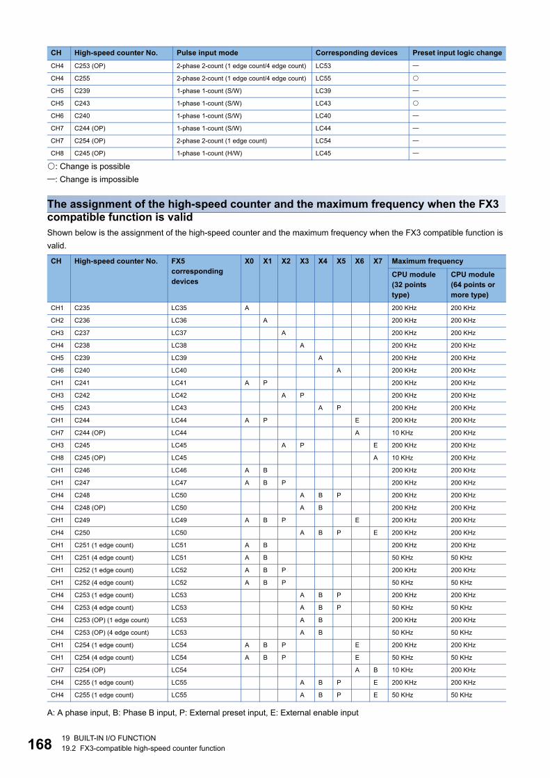
16819 BUILT-IN I/O FUNCTION
19.2 FX3-compatible high-speed counter function
: Change is possible
: Change is impossible
The assignment of the high-speed counter and the maximum frequency when the FX3 compatible function is valid
Shown below is the assignment of the high-speed counter and the maximum frequency when the FX3 compatible function is
valid.
A: A phase input, B: Phase B input, P: External preset input, E: External enable input
CH4 C253 (OP) 2-phase 2-count (1 edge count/4 edge count) LC53
CH4 C255 2-phase 2-count (1 edge count/4 edge count) LC55
CH5 C239 1-phase 1-count (S/W) LC39
CH5 C243 1-phase 1-count (S/W) LC43
CH6 C240 1-phase 1-count (S/W) LC40
CH7 C244 (OP) 1-phase 1-count (S/W) LC44
CH7 C254 (OP) 2-phase 2-count (1 edge count) LC54
CH8 C245 (OP) 1-phase 1-count (H/W) LC45
CH High-speed counter No. FX5
corresponding
devices
X0 X1 X2 X3 X4 X5 X6 X7 Maximum frequency
CPU module
(32 points
type)
CPU module
(64 points or
more type)
CH1 C235 LC35 A 200 KHz 200 KHz
CH2 C236 LC36 A 200 KHz 200 KHz
CH3 C237 LC37 A 200 KHz 200 KHz
CH4 C238 LC38 A 200 KHz 200 KHz
CH5 C239 LC39 A 200 KHz 200 KHz
CH6 C240 LC40 A 200 KHz 200 KHz
CH1 C241 LC41 A P 200 KHz 200 KHz
CH3 C242 LC42 A P 200 KHz 200 KHz
CH5 C243 LC43 A P 200 KHz 200 KHz
CH1 C244 LC44 A P E 200 KHz 200 KHz
CH7 C244 (OP) LC44 A 10 KHz 200 KHz
CH3 C245 LC45 A P E 200 KHz 200 KHz
CH8 C245 (OP) LC45 A 10 KHz 200 KHz
CH1 C246 LC46 A B 200 KHz 200 KHz
CH1 C247 LC47 A B P 200 KHz 200 KHz
CH4 C248 LC50 A B P 200 KHz 200 KHz
CH4 C248 (OP) LC50 A B 200 KHz 200 KHz
CH1 C249 LC49 A B P E 200 KHz 200 KHz
CH4 C250 LC50 A B P E 200 KHz 200 KHz
CH1 C251 (1 edge count) LC51 A B 200 KHz 200 KHz
CH1 C251 (4 edge count) LC51 A B 50 KHz 50 KHz
CH1 C252 (1 edge count) LC52 A B P 200 KHz 200 KHz
CH1 C252 (4 edge count) LC52 A B P 50 KHz 50 KHz
CH4 C253 (1 edge count) LC53 A B P 200 KHz 200 KHz
CH4 C253 (4 edge count) LC53 A B P 50 KHz 50 KHz
CH4 C253 (OP) (1 edge count) LC53 A B 200 KHz 200 KHz
CH4 C253 (OP) (4 edge count) LC53 A B 50 KHz 50 KHz
CH1 C254 (1 edge count) LC54 A B P E 200 KHz 200 KHz
CH1 C254 (4 edge count) LC54 A B P E 50 KHz 50 KHz
CH7 C254 (OP) LC54 A B 10 KHz 200 KHz
CH4 C255 (1 edge count) LC55 A B P E 200 KHz 200 KHz
CH4 C255 (1 edge count) LC55 A B P E 50 KHz 50 KHz
CH High-speed counter No. Pulse input mode Corresponding devices Preset input logic change
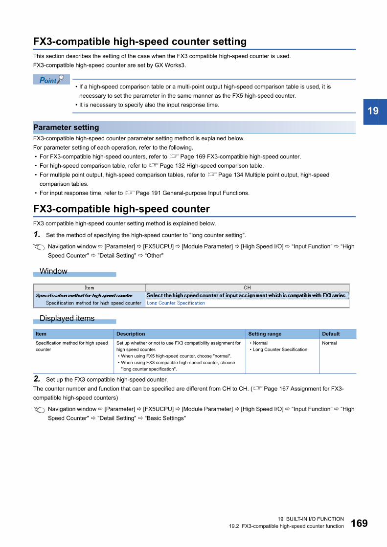
19 BUILT-IN I/O FUNCTION
19.2 FX3-compatible high-speed counter function 169
19
FX3-compatible high-speed counter setting
This section describes the setting of the case when the FX3 compatible high-speed counter is used.
FX3-compatible high-speed counter are set by GX Works3.
� If a high-speed comparison table or a multi-point output high-speed comparison table is used, it is
necessary to set the parameter in the same manner as the FX5 high-speed counter.
� It is necessary to specify also the input response time.
Parameter setting
FX3-compatible high-speed counter parameter setting method is explained below.
For parameter setting of each operation, refer to the following.
� For FX3-compatible high-speed counters, refer to Page 169 FX3-compatible high-speed counter.
� For high-speed comparison table, refer to Page 132 High-speed comparison table.
� For multiple point output, high-speed comparison tables, refer to Page 134 Multiple point output, high-speed
comparison tables.
� For input response time, refer to Page 191 General-purpose Input Functions.
FX3-compatible high-speed counter
FX3 compatible high-speed counter setting method is explained below.
1. Set the method of specifying the high-speed counter to "long counter setting".
Navigation window [Parameter] [FX5UCPU] [Module Parameter] [High Speed I/O] “Input Function" “High
Speed Counter" "Detail Setting" “Other"
Window
Displayed items
2. Set up the FX3 compatible high-speed counter.
The counter number and function that can be specified are different from CH to CH. (Page 167 Assignment for FX3-
compatible high-speed counters)
Navigation window [Parameter] [FX5UCPU] [Module Parameter] [High Speed I/O] “Input Function" “High
Speed Counter" "Detail Setting" “Basic Settings"
Item Description Setting range Default
Specification method for high speed
counter
Set up whether or not to use FX3 compatibility assignment for
high speed counter.
� When using FX5 high-speed counter, choose "normal".
� When using FX3 compatible high-speed counter, choose
"long counter specification".
� Normal
� Long Counter Specification
Normal
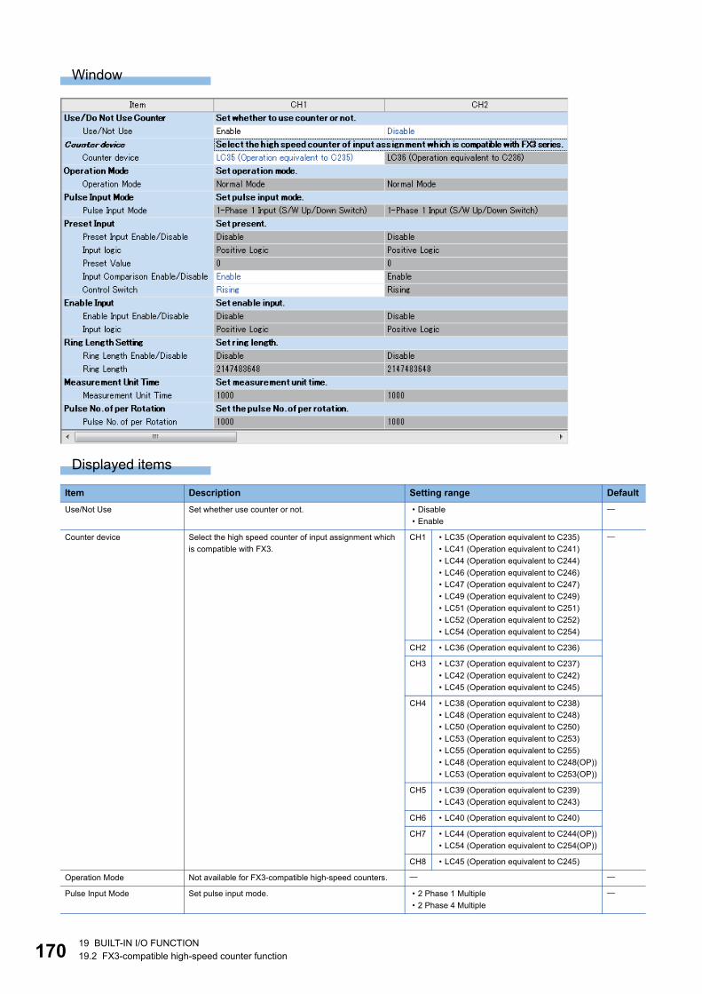
17019 BUILT-IN I/O FUNCTION
19.2 FX3-compatible high-speed counter function
Window
Displayed items
Item Description Setting range Default
Use/Not Use Set whether use counter or not. � Disable
� Enable
Counter device Select the high speed counter of input assignment which
is compatible with FX3.
CH1 � LC35 (Operation equivalent to C235)
� LC41 (Operation equivalent to C241)
� LC44 (Operation equivalent to C244)
� LC46 (Operation equivalent to C246)
� LC47 (Operation equivalent to C247)
� LC49 (Operation equivalent to C249)
� LC51 (Operation equivalent to C251)
� LC52 (Operation equivalent to C252)
� LC54 (Operation equivalent to C254)
CH2 � LC36 (Operation equivalent to C236)
CH3 � LC37 (Operation equivalent to C237)
� LC42 (Operation equivalent to C242)
� LC45 (Operation equivalent to C245)
CH4 � LC38 (Operation equivalent to C238)
� LC48 (Operation equivalent to C248)
� LC50 (Operation equivalent to C250)
� LC53 (Operation equivalent to C253)
� LC55 (Operation equivalent to C255)
� LC48 (Operation equivalent to C248(OP))
� LC53 (Operation equivalent to C253(OP))
CH5 � LC39 (Operation equivalent to C239)
� LC43 (Operation equivalent to C243)
CH6 � LC40 (Operation equivalent to C240)
CH7 � LC44 (Operation equivalent to C244(OP))
� LC54 (Operation equivalent to C254(OP))
CH8 � LC45 (Operation equivalent to C245)
Operation Mode Not available for FX3-compatible high-speed counters.
Pulse Input Mode Set pulse input mode. � 2 Phase 1 Multiple
� 2 Phase 4 Multiple
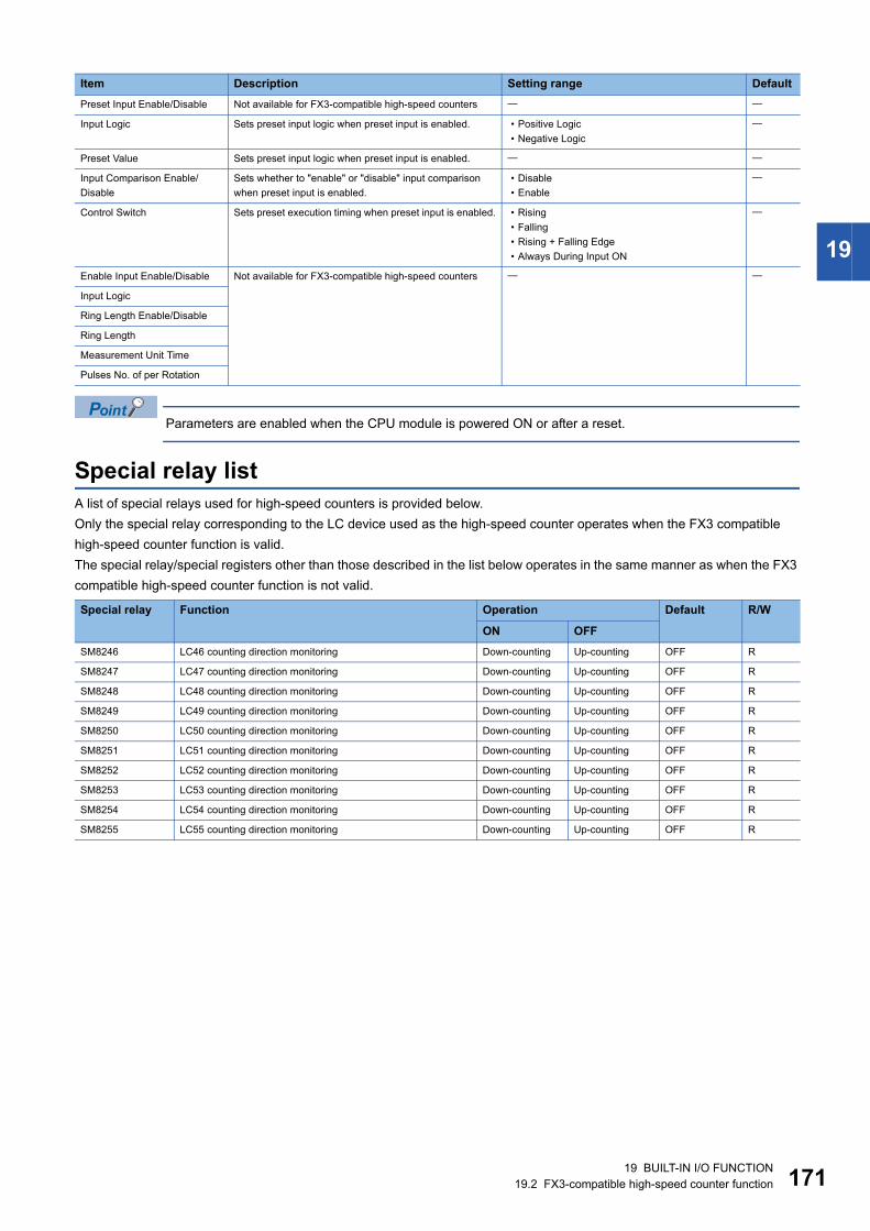
19 BUILT-IN I/O FUNCTION
19.2 FX3-compatible high-speed counter function 171
19
Parameters are enabled when the CPU module is powered ON or after a reset.
Special relay list
A list of special relays used for high-speed counters is provided below.
Only the special relay corresponding to the LC device used as the high-speed counter operates when the FX3 compatible
high-speed counter function is valid.
The special relay/special registers other than those described in the list below operates in the same manner as when the FX3
compatible high-speed counter function is not valid.
Preset Input Enable/Disable Not available for FX3-compatible high-speed counters
Input Logic Sets preset input logic when preset input is enabled. � Positive Logic
� Negative Logic
Preset Value Sets preset input logic when preset input is enabled.
Input Comparison Enable/
Disable
Sets whether to "enable" or "disable" input comparison
when preset input is enabled.
� Disable
� Enable
Control Switch Sets preset execution timing when preset input is enabled. � Rising
� Falling
� Rising + Falling Edge
� Always During Input ON
Enable Input Enable/Disable Not available for FX3-compatible high-speed counters
Input Logic
Ring Length Enable/Disable
Ring Length
Measurement Unit Time
Pulses No. of per Rotation
Special relay Function Operation Default R/W
ON OFF
SM8246 LC46 counting direction monitoring Down-counting Up-counting OFF R
SM8247 LC47 counting direction monitoring Down-counting Up-counting OFF R
SM8248 LC48 counting direction monitoring Down-counting Up-counting OFF R
SM8249 LC49 counting direction monitoring Down-counting Up-counting OFF R
SM8250 LC50 counting direction monitoring Down-counting Up-counting OFF R
SM8251 LC51 counting direction monitoring Down-counting Up-counting OFF R
SM8252 LC52 counting direction monitoring Down-counting Up-counting OFF R
SM8253 LC53 counting direction monitoring Down-counting Up-counting OFF R
SM8254 LC54 counting direction monitoring Down-counting Up-counting OFF R
SM8255 LC55 counting direction monitoring Down-counting Up-counting OFF R
Item Description Setting range Default
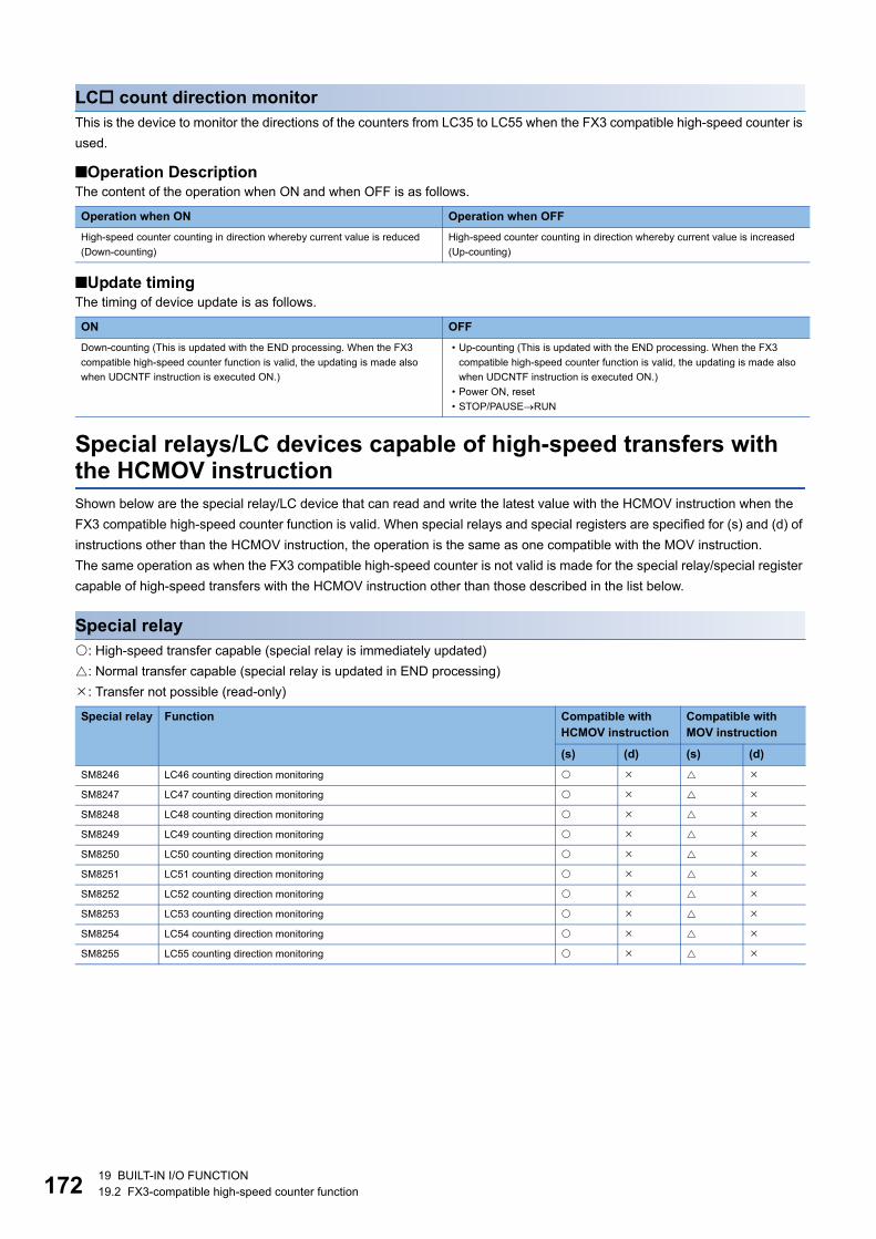
17219 BUILT-IN I/O FUNCTION
19.2 FX3-compatible high-speed counter function
LC count direction monitor
This is the device to monitor the directions of the counters from LC35 to LC55 when the FX3 compatible high-speed counter is
used.
■Operation DescriptionThe content of the operation when ON and when OFF is as follows.
■Update timingThe timing of device update is as follows.
Special relays/LC devices capable of high-speed transfers with the HCMOV instruction
Shown below are the special relay/LC device that can read and write the latest value with the HCMOV instruction when the
FX3 compatible high-speed counter function is valid. When special relays and special registers are specified for (s) and (d) of
instructions other than the HCMOV instruction, the operation is the same as one compatible with the MOV instruction.
The same operation as when the FX3 compatible high-speed counter is not valid is made for the special relay/special register
capable of high-speed transfers with the HCMOV instruction other than those described in the list below.
Special relay
: High-speed transfer capable (special relay is immediately updated)
: Normal transfer capable (special relay is updated in END processing)
: Transfer not possible (read-only)
Operation when ON Operation when OFF
High-speed counter counting in direction whereby current value is reduced
(Down-counting)
High-speed counter counting in direction whereby current value is increased
(Up-counting)
ON OFF
Down-counting (This is updated with the END processing. When the FX3
compatible high-speed counter function is valid, the updating is made also
when UDCNTF instruction is executed ON.)
� Up-counting (This is updated with the END processing. When the FX3
compatible high-speed counter function is valid, the updating is made also
when UDCNTF instruction is executed ON.)
� Power ON, reset
� STOP/PAUSERUN
Special relay Function Compatible with
HCMOV instruction
Compatible with
MOV instruction
(s) (d) (s) (d)
SM8246 LC46 counting direction monitoring
SM8247 LC47 counting direction monitoring
SM8248 LC48 counting direction monitoring
SM8249 LC49 counting direction monitoring
SM8250 LC50 counting direction monitoring
SM8251 LC51 counting direction monitoring
SM8252 LC52 counting direction monitoring
SM8253 LC53 counting direction monitoring
SM8254 LC54 counting direction monitoring
SM8255 LC55 counting direction monitoring
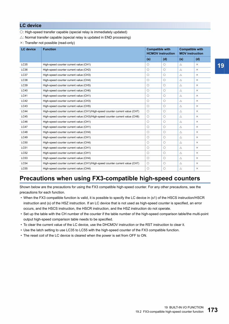
19 BUILT-IN I/O FUNCTION
19.2 FX3-compatible high-speed counter function 173
19
LC device
: High-speed transfer capable (special relay is immediately updated)
: Normal transfer capable (special relay is updated in END processing)
: Transfer not possible (read-only)
Precautions when using FX3-compatible high-speed counters
Shown below are the precautions for using the FX3 compatible high-speed counter. For any other precautions, see the
precautions for each function.
� When the FX3 compatible function is valid, it is possible to specify the LC device in (s1) of the HSCS instruction/HSCR
instruction and (s) of the HSZ instruction. If an LC device that is not used as high-speed counter is specified, an error
occurs, and the HSCS instruction, the HSCR instruction, and the HSZ instruction do not operate.
� Set up the table with the CH number of the counter if the table number of the high-speed comparison table/the multi-point
output high-speed comparison table needs to be specified.
� To clear the current value of the LC device, use the DHCMOV instruction or the RST instruction to clear it.
� Use the latch setting to use LC35 to LC55 with the high-speed counter of the FX3 compatible function.
� The reset coil of the LC device is cleared when the power is set from OFF to ON.
LC device Function Compatible with
HCMOV instruction
Compatible with
MOV instruction
(s) (d) (s) (d)
LC35 High-speed counter current value (CH1)
LC36 High-speed counter current value (CH2)
LC37 High-speed counter current value (CH3)
LC38 High-speed counter current value (CH4)
LC39 High-speed counter current value (CH5)
LC40 High-speed counter current value (CH6)
LC41 High-speed counter current value (CH1)
LC42 High-speed counter current value (CH3)
LC43 High-speed counter current value (CH5)
LC44 High-speed counter current value (CH1)/High-speed counter current value (CH7)
LC45 High-speed counter current value (CH3)/High-speed counter current value (CH8)
LC46 High-speed counter current value (CH1)
LC47 High-speed counter current value (CH1)
LC48 High-speed counter current value (CH4)
LC49 High-speed counter current value (CH1)
LC50 High-speed counter current value (CH4)
LC51 High-speed counter current value (CH1)
LC52 High-speed counter current value (CH1)
LC53 High-speed counter current value (CH4)
LC54 High-speed counter current value (CH1)/High-speed counter current value (CH7)
LC55 High-speed counter current value (CH4)
17419 BUILT-IN I/O FUNCTION
19.3 Pulse Width Measurement Function
19.3 Pulse Width Measurement Function
This section describes the pulse width measurement function.
Pulse width measurement function overview
The CPU module has a built-in pulse width measurement function and it is capable of measuring the pulse width/period of a
maximum of 4 channels. The pulse width/period measurement function stores the values of 0.5 s ring counters at the input
signal rising edge and falling edge to special data registers. This function also stores the difference in the counter values
(pulse width) between the rising edge and the falling edge or stores the difference in the counter values (cycle) between the
previous rising edge and the current rising edge to special data registers in units of 0.5 s.
For the pulse width measurement function, input channel assignments, logical switch, and measurement mode settings are
configured with parameters, and measurements are started/stopped using the HIOEN instruction.
To use the pulse width measurement function, parameter settings and the HIOEN instruction are always
required.
Pulse width measurement specifications
This section describes the pulse width measurement function specifications.
Pulse input signals
Pulse width measurements can be used for a maximum of 4 channels.
Select from X0 to X7 for each channel, with parameter settings.
■Measurement frequenciesThe table below shows the measurement frequencies.
■Measurement precisionThe table below shows the measurement precision.
Pulse measurements
The pulse width and period are stored in special devices by the END instruction. (Page 177 List of special relays/special
registers)
Pulse width maximum value and minimum value
The maximum value and minimum value of the pulse width from the start of measurements are stored in special devices.
(Page 177 List of special relays/special registers)
Period maximum value and minimum value
The maximum value and minimum value of the period from the start of measurements are stored in special devices.
(Page 177 List of special relays/special registers)
FX5U-32M, FX5UC-32M FX5U-64M, FX5U-80M Measurement frequencies
X0 to X5 X0 to X7 200 KHz
X6 to X17 X10 to X17 10 KHz
Item Description
Possible measurement range Cycle 5 s
Pulse width 5 s
Maximum measurable signal width 1073s741ms823s
Resolution 0.5 s
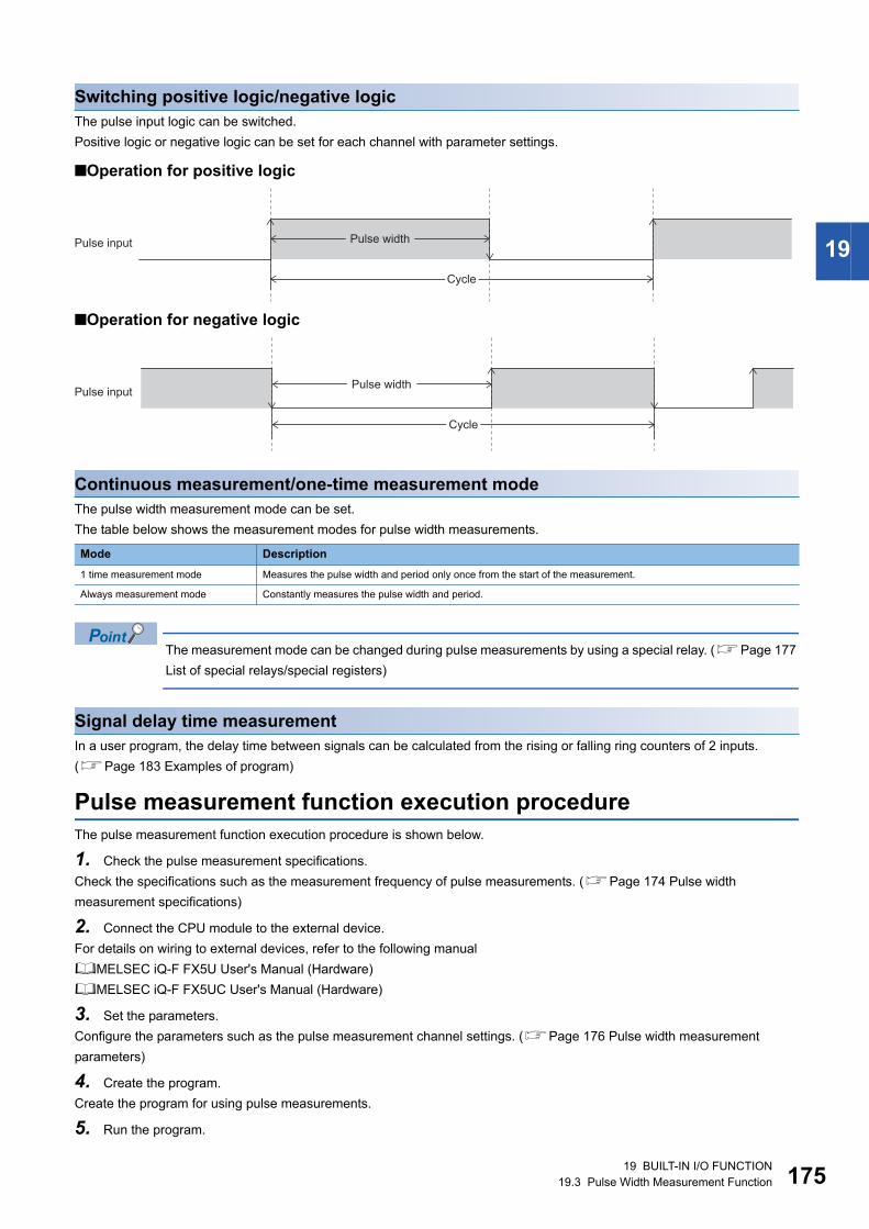
19 BUILT-IN I/O FUNCTION
19.3 Pulse Width Measurement Function 175
19
Switching positive logic/negative logic
The pulse input logic can be switched.
Positive logic or negative logic can be set for each channel with parameter settings.
■Operation for positive logic
■Operation for negative logic
Continuous measurement/one-time measurement mode
The pulse width measurement mode can be set.
The table below shows the measurement modes for pulse width measurements.
The measurement mode can be changed during pulse measurements by using a special relay. (Page 177
List of special relays/special registers)
Signal delay time measurement
In a user program, the delay time between signals can be calculated from the rising or falling ring counters of 2 inputs.
(Page 183 Examples of program)
Pulse measurement function execution procedure
The pulse measurement function execution procedure is shown below.
1. Check the pulse measurement specifications.
Check the specifications such as the measurement frequency of pulse measurements. (Page 174 Pulse width
measurement specifications)
2. Connect the CPU module to the external device.
For details on wiring to external devices, refer to the following manual
MELSEC iQ-F FX5U User's Manual (Hardware)
MELSEC iQ-F FX5UC User's Manual (Hardware)
3. Set the parameters.
Configure the parameters such as the pulse measurement channel settings. (Page 176 Pulse width measurement
parameters)
4. Create the program.
Create the program for using pulse measurements.
5. Run the program.
Mode Description
1 time measurement mode Measures the pulse width and period only once from the start of the measurement.
Always measurement mode Constantly measures the pulse width and period.
Pulse input Pulse width
Cycle
Pulse inputPulse width
Cycle
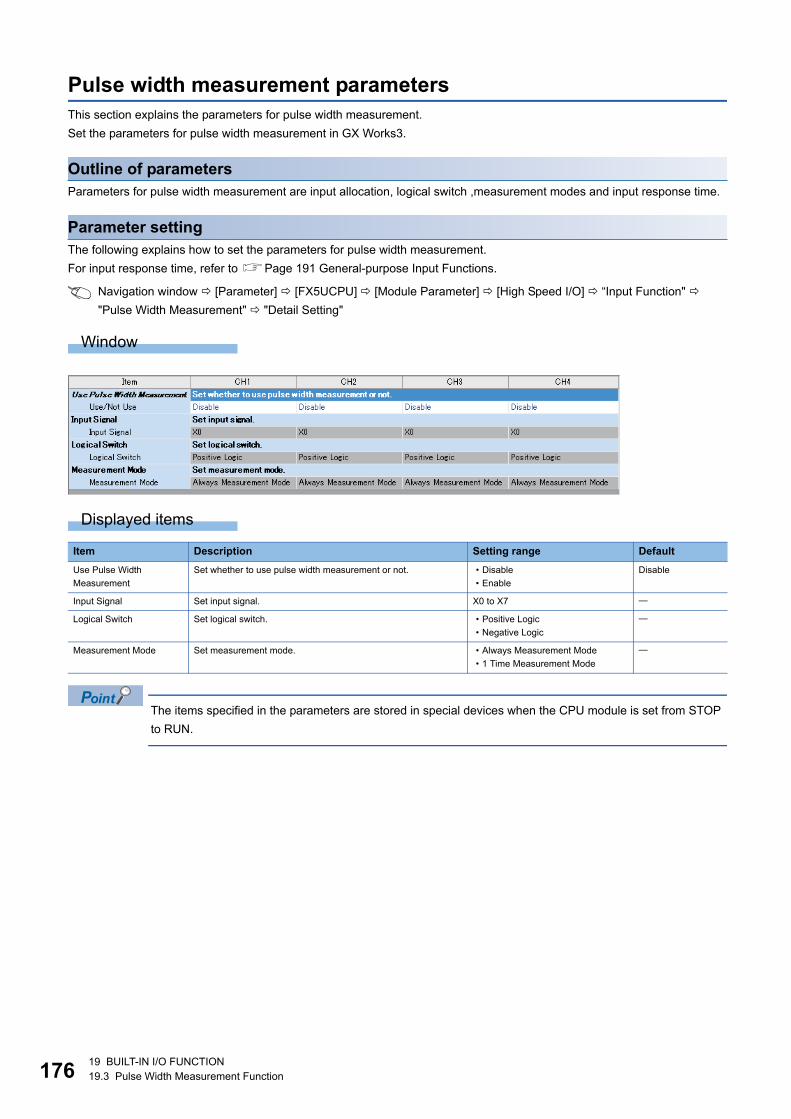
17619 BUILT-IN I/O FUNCTION
19.3 Pulse Width Measurement Function
Pulse width measurement parameters
This section explains the parameters for pulse width measurement.
Set the parameters for pulse width measurement in GX Works3.
Outline of parameters
Parameters for pulse width measurement are input allocation, logical switch ,measurement modes and input response time.
Parameter setting
The following explains how to set the parameters for pulse width measurement.
For input response time, refer to Page 191 General-purpose Input Functions.
Navigation window [Parameter] [FX5UCPU] [Module Parameter] [High Speed I/O] “Input Function"
"Pulse Width Measurement" "Detail Setting"
Window
Displayed items
The items specified in the parameters are stored in special devices when the CPU module is set from STOP
to RUN.
Item Description Setting range Default
Use Pulse Width
Measurement
Set whether to use pulse width measurement or not. � Disable
� Enable
Disable
Input Signal Set input signal. X0 to X7
Logical Switch Set logical switch. � Positive Logic
� Negative Logic
Measurement Mode Set measurement mode. � Always Measurement Mode
� 1 Time Measurement Mode
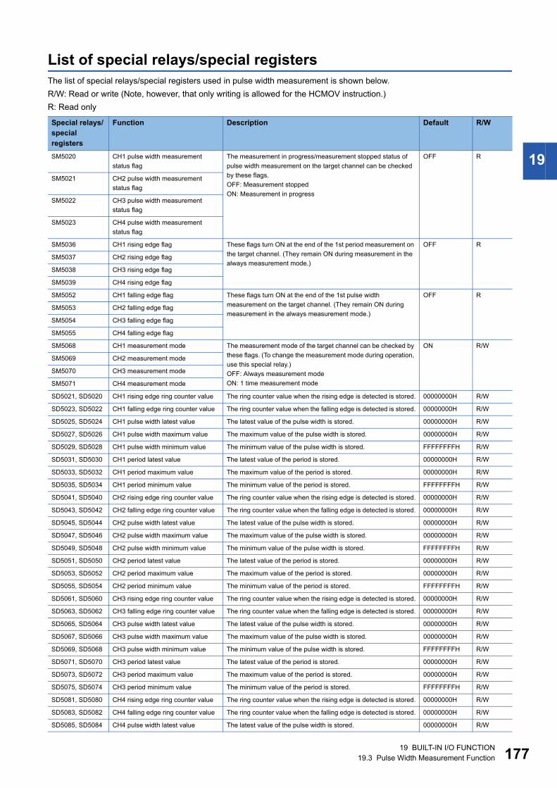
19 BUILT-IN I/O FUNCTION
19.3 Pulse Width Measurement Function 177
19
List of special relays/special registers
The list of special relays/special registers used in pulse width measurement is shown below.
R/W: Read or write (Note, however, that only writing is allowed for the HCMOV instruction.)
R: Read only
Special relays/
special
registers
Function Description Default R/W
SM5020 CH1 pulse width measurement
status flag
The measurement in progress/measurement stopped status of
pulse width measurement on the target channel can be checked
by these flags.
OFF: Measurement stopped
ON: Measurement in progress
OFF R
SM5021 CH2 pulse width measurement
status flag
SM5022 CH3 pulse width measurement
status flag
SM5023 CH4 pulse width measurement
status flag
SM5036 CH1 rising edge flag These flags turn ON at the end of the 1st period measurement on
the target channel. (They remain ON during measurement in the
always measurement mode.)
OFF R
SM5037 CH2 rising edge flag
SM5038 CH3 rising edge flag
SM5039 CH4 rising edge flag
SM5052 CH1 falling edge flag These flags turn ON at the end of the 1st pulse width
measurement on the target channel. (They remain ON during
measurement in the always measurement mode.)
OFF R
SM5053 CH2 falling edge flag
SM5054 CH3 falling edge flag
SM5055 CH4 falling edge flag
SM5068 CH1 measurement mode The measurement mode of the target channel can be checked by
these flags. (To change the measurement mode during operation,
use this special relay.)
OFF: Always measurement mode
ON: 1 time measurement mode
ON R/W
SM5069 CH2 measurement mode
SM5070 CH3 measurement mode
SM5071 CH4 measurement mode
SD5021, SD5020 CH1 rising edge ring counter value The ring counter value when the rising edge is detected is stored. 00000000H R/W
SD5023, SD5022 CH1 falling edge ring counter value The ring counter value when the falling edge is detected is stored. 00000000H R/W
SD5025, SD5024 CH1 pulse width latest value The latest value of the pulse width is stored. 00000000H R/W
SD5027, SD5026 CH1 pulse width maximum value The maximum value of the pulse width is stored. 00000000H R/W
SD5029, SD5028 CH1 pulse width minimum value The minimum value of the pulse width is stored. FFFFFFFFH R/W
SD5031, SD5030 CH1 period latest value The latest value of the period is stored. 00000000H R/W
SD5033, SD5032 CH1 period maximum value The maximum value of the period is stored. 00000000H R/W
SD5035, SD5034 CH1 period minimum value The minimum value of the period is stored. FFFFFFFFH R/W
SD5041, SD5040 CH2 rising edge ring counter value The ring counter value when the rising edge is detected is stored. 00000000H R/W
SD5043, SD5042 CH2 falling edge ring counter value The ring counter value when the falling edge is detected is stored. 00000000H R/W
SD5045, SD5044 CH2 pulse width latest value The latest value of the pulse width is stored. 00000000H R/W
SD5047, SD5046 CH2 pulse width maximum value The maximum value of the pulse width is stored. 00000000H R/W
SD5049, SD5048 CH2 pulse width minimum value The minimum value of the pulse width is stored. FFFFFFFFH R/W
SD5051, SD5050 CH2 period latest value The latest value of the period is stored. 00000000H R/W
SD5053, SD5052 CH2 period maximum value The maximum value of the period is stored. 00000000H R/W
SD5055, SD5054 CH2 period minimum value The minimum value of the period is stored. FFFFFFFFH R/W
SD5061, SD5060 CH3 rising edge ring counter value The ring counter value when the rising edge is detected is stored. 00000000H R/W
SD5063, SD5062 CH3 falling edge ring counter value The ring counter value when the falling edge is detected is stored. 00000000H R/W
SD5065, SD5064 CH3 pulse width latest value The latest value of the pulse width is stored. 00000000H R/W
SD5067, SD5066 CH3 pulse width maximum value The maximum value of the pulse width is stored. 00000000H R/W
SD5069, SD5068 CH3 pulse width minimum value The minimum value of the pulse width is stored. FFFFFFFFH R/W
SD5071, SD5070 CH3 period latest value The latest value of the period is stored. 00000000H R/W
SD5073, SD5072 CH3 period maximum value The maximum value of the period is stored. 00000000H R/W
SD5075, SD5074 CH3 period minimum value The minimum value of the period is stored. FFFFFFFFH R/W
SD5081, SD5080 CH4 rising edge ring counter value The ring counter value when the rising edge is detected is stored. 00000000H R/W
SD5083, SD5082 CH4 falling edge ring counter value The ring counter value when the falling edge is detected is stored. 00000000H R/W
SD5085, SD5084 CH4 pulse width latest value The latest value of the pulse width is stored. 00000000H R/W
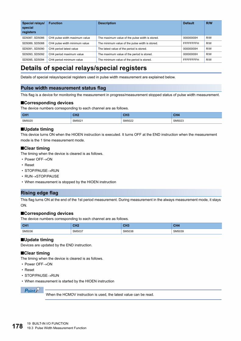
17819 BUILT-IN I/O FUNCTION
19.3 Pulse Width Measurement Function
Details of special relays/special registers
Details of special relays/special registers used in pulse width measurement are explained below.
Pulse width measurement status flag
This flag is a device for monitoring the measurement in progress/measurement stopped status of pulse width measurement.
■Corresponding devicesThe device numbers corresponding to each channel are as follows.
■Update timingThis device turns ON when the HIOEN instruction is executed. It turns OFF at the END instruction when the measurement
mode is the 1 time measurement mode.
■Clear timingThe timing when the device is cleared is as follows.
� Power OFFON
� Reset
� STOP/PAUSERUN
� RUNSTOP/PAUSE
� When measurement is stopped by the HIOEN instruction
Rising edge flag
This flag turns ON at the end of the 1st period measurement. During measurement in the always measurement mode, it stays
ON.
■Corresponding devicesThe device numbers corresponding to each channel are as follows.
■Update timingDevices are updated by the END instruction.
■Clear timingThe timing when the device is cleared is as follows.
� Power OFFON
� Reset
� STOP/PAUSERUN
� When measurement is started by the HIOEN instruction
When the HCMOV instruction is used, the latest value can be read.
SD5087, SD5086 CH4 pulse width maximum value The maximum value of the pulse width is stored. 00000000H R/W
SD5089, SD5088 CH4 pulse width minimum value The minimum value of the pulse width is stored. FFFFFFFFH R/W
SD5091, SD5090 CH4 period latest value The latest value of the period is stored. 00000000H R/W
SD5093, SD5092 CH4 period maximum value The maximum value of the period is stored. 00000000H R/W
SD5095, SD5094 CH4 period minimum value The minimum value of the period is stored. FFFFFFFFH R/W
CH1 CH2 CH3 CH4
SM5020 SM5021 SM5022 SM5023
CH1 CH2 CH3 CH4
SM5036 SM5037 SM5038 SM5039
Special relays/
special
registers
Function Description Default R/W
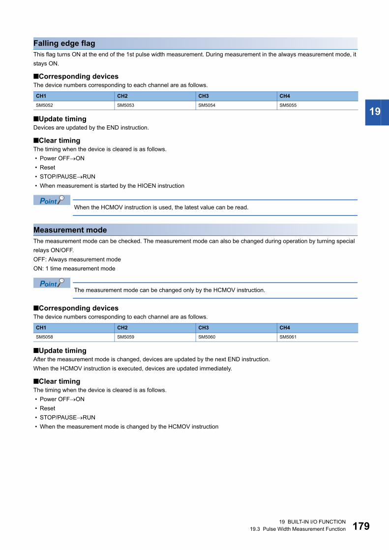
19 BUILT-IN I/O FUNCTION
19.3 Pulse Width Measurement Function 179
19
Falling edge flag
This flag turns ON at the end of the 1st pulse width measurement. During measurement in the always measurement mode, it
stays ON.
■Corresponding devicesThe device numbers corresponding to each channel are as follows.
■Update timingDevices are updated by the END instruction.
■Clear timingThe timing when the device is cleared is as follows.
� Power OFFON
� Reset
� STOP/PAUSERUN
� When measurement is started by the HIOEN instruction
When the HCMOV instruction is used, the latest value can be read.
Measurement mode
The measurement mode can be checked. The measurement mode can also be changed during operation by turning special
relays ON/OFF.
OFF: Always measurement mode
ON: 1 time measurement mode
The measurement mode can be changed only by the HCMOV instruction.
■Corresponding devicesThe device numbers corresponding to each channel are as follows.
■Update timingAfter the measurement mode is changed, devices are updated by the next END instruction.
When the HCMOV instruction is executed, devices are updated immediately.
■Clear timingThe timing when the device is cleared is as follows.
� Power OFFON
� Reset
� STOP/PAUSERUN
� When the measurement mode is changed by the HCMOV instruction
CH1 CH2 CH3 CH4
SM5052 SM5053 SM5054 SM5055
CH1 CH2 CH3 CH4
SM5058 SM5059 SM5060 SM5061
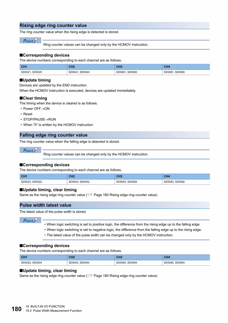
18019 BUILT-IN I/O FUNCTION
19.3 Pulse Width Measurement Function
Rising edge ring counter value
The ring counter value when the rising edge is detected is stored.
Ring counter values can be changed only by the HCMOV instruction.
■Corresponding devicesThe device numbers corresponding to each channel are as follows.
■Update timingDevices are updated by the END instruction.
When the HCMOV instruction is executed, devices are updated immediately.
■Clear timingThe timing when the device is cleared is as follows.
� Power OFFON
� Reset
� STOP/PAUSERUN
� When "0" is written by the HCMOV instruction
Falling edge ring counter value
The ring counter value when the falling edge is detected is stored.
Ring counter values can be changed only by the HCMOV instruction.
■Corresponding devicesThe device numbers corresponding to each channel are as follows.
■Update timing, clear timingSame as the rising edge ring counter value (Page 180 Rising edge ring counter value)
Pulse width latest value
The latest value of the pulse width is stored.
� When logic switching is set to positive logic, the difference from the rising edge up to the falling edge.
� When logic switching is set to negative logic, the difference from the falling edge up to the rising edge.
� The latest value of the pulse width can be changed only by the HCMOV instruction.
■Corresponding devicesThe device numbers corresponding to each channel are as follows.
■Update timing, clear timingSame as the rising edge ring counter value (Page 180 Rising edge ring counter value)
CH1 CH2 CH3 CH4
SD5021, SD5020 SD5041, SD5040 SD5061, SD5060 SD5081, SD5080
CH1 CH2 CH3 CH4
SD5023, SD5022 SD5043, SD5042 SD5063, SD5062 SD5083, SD5082
CH1 CH2 CH3 CH4
SD5025, SD5024 SD5045, SD5044 SD5065, SD5064 SD5085, SD5084
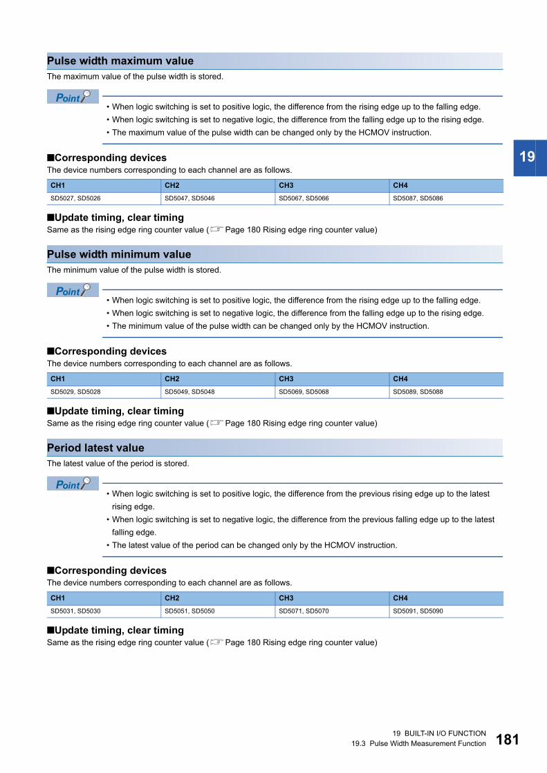
19 BUILT-IN I/O FUNCTION
19.3 Pulse Width Measurement Function 181
19
Pulse width maximum value
The maximum value of the pulse width is stored.
� When logic switching is set to positive logic, the difference from the rising edge up to the falling edge.
� When logic switching is set to negative logic, the difference from the falling edge up to the rising edge.
� The maximum value of the pulse width can be changed only by the HCMOV instruction.
■Corresponding devicesThe device numbers corresponding to each channel are as follows.
■Update timing, clear timingSame as the rising edge ring counter value (Page 180 Rising edge ring counter value)
Pulse width minimum value
The minimum value of the pulse width is stored.
� When logic switching is set to positive logic, the difference from the rising edge up to the falling edge.
� When logic switching is set to negative logic, the difference from the falling edge up to the rising edge.
� The minimum value of the pulse width can be changed only by the HCMOV instruction.
■Corresponding devicesThe device numbers corresponding to each channel are as follows.
■Update timing, clear timingSame as the rising edge ring counter value (Page 180 Rising edge ring counter value)
Period latest value
The latest value of the period is stored.
� When logic switching is set to positive logic, the difference from the previous rising edge up to the latest
rising edge.
� When logic switching is set to negative logic, the difference from the previous falling edge up to the latest
falling edge.
� The latest value of the period can be changed only by the HCMOV instruction.
■Corresponding devicesThe device numbers corresponding to each channel are as follows.
■Update timing, clear timingSame as the rising edge ring counter value (Page 180 Rising edge ring counter value)
CH1 CH2 CH3 CH4
SD5027, SD5026 SD5047, SD5046 SD5067, SD5066 SD5087, SD5086
CH1 CH2 CH3 CH4
SD5029, SD5028 SD5049, SD5048 SD5069, SD5068 SD5089, SD5088
CH1 CH2 CH3 CH4
SD5031, SD5030 SD5051, SD5050 SD5071, SD5070 SD5091, SD5090
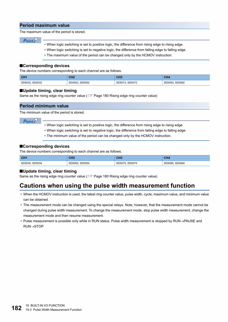
18219 BUILT-IN I/O FUNCTION
19.3 Pulse Width Measurement Function
Period maximum value
The maximum value of the period is stored.
� When logic switching is set to positive logic, the difference from rising edge to rising edge.
� When logic switching is set to negative logic, the difference from falling edge to falling edge.
� The maximum value of the period can be changed only by the HCMOV instruction.
■Corresponding devicesThe device numbers corresponding to each channel are as follows.
■Update timing, clear timingSame as the rising edge ring counter value (Page 180 Rising edge ring counter value)
Period minimum value
The minimum value of the period is stored.
� When logic switching is set to positive logic, the difference from rising edge to rising edge.
� When logic switching is set to negative logic, the difference from falling edge to falling edge.
� The minimum value of the period can be changed only by the HCMOV instruction.
■Corresponding devicesThe device numbers corresponding to each channel are as follows.
■Update timing, clear timingSame as the rising edge ring counter value (Page 180 Rising edge ring counter value)
Cautions when using the pulse width measurement function
� When the HCMOV instruction is used, the latest ring counter value, pulse width, cycle, maximum value, and minimum value
can be obtained.
� The measurement mode can be changed using the special relays. Note, however, that the measurement mode cannot be
changed during pulse width measurement. To change the measurement mode, stop pulse width measurement, change the
measurement mode and then resume measurement.
� Pulse measurement is possible only while in RUN status. Pulse width measurement is stopped by RUNPAUSE and
RUNSTOP.
CH1 CH2 CH3 CH4
SD5033, SD5032 SD5053, SD5052 SD5073, SD5072 SD5093, SD5092
CH1 CH2 CH3 CH4
SD5035, SD5034 SD5055, SD5054 SD5075, SD5074 SD5095, SD5094
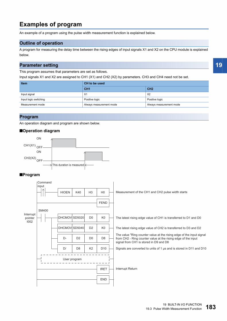
19 BUILT-IN I/O FUNCTION
19.3 Pulse Width Measurement Function 183
19
Examples of program
An example of a program using the pulse width measurement function is explained below.
Outline of operation
A program for measuring the delay time between the rising edges of input signals X1 and X2 on the CPU module is explained
below.
Parameter setting
This program assumes that parameters are set as follows.
Input signals X1 and X2 are assigned to CH1 (X1) and CH2 (X2) by parameters. CH3 and CH4 need not be set.
Program
An operation diagram and program are shown below.
■Operation diagram
■Program
Item CH to be used
CH1 CH2
Input signal X1 X2
Input logic switching Positive logic Positive logic
Measurement mode Always measurement mode Always measurement mode
CH1(X1)
ON
OFF
This duration is measured
CH2(X2)
ON
OFF
HIOEN H3 H0K40
FEND
SM400
DHCMOV SD5020 D0
END
The latest rising edge value of CH2 is transferred to D3 and D2
Measurement of the CH1 and CH2 pulse width starts
DHCMOV SD5040 D2
User program
IRET
The latest rising edge value of CH1 is transferred to D1 and D0
Interrupt Return
K0
K0
D- D2 D0 D8
D/ D8 K2 D10 Signals are converted to units of 1 μs and is stored in D11 and D10
Interrupt
pointer
I002
Command
input
The value "Ring counter value at the rising edge of the input signal
from CH2 - Ring counter value at the rising edge of the input
signal from CH1 is stored in D9 and D8
18419 BUILT-IN I/O FUNCTION
19.4 Pulse Catch Function
19.4 Pulse Catch Function
This section explains the pulse catch function.
Outline of pulse catch function
The CPU module has a built-in pulse catch function which enables pulse signals that are incompletely sampled in regular
input processing to be caught. Inputs X0 to X17 on the CPU module can be used on up to eight channels.
To use the pulse catch function, pulse catch setting and the input response time must be set with parameters.
An FX3-compatible pulse catch function is also mounted on the CPU module, For details of functions, refer to Page 188
FX3-Compatible Pulse Catch Function.
The pulse catch function and FX3-compatible pulse catch function can be used simultaneously.
Specifications of pulse catch function
The specifications of the pulse catch function are explained below.
Performance specifications
Pulse catches can be used on inputs X0 to X17.
■Input response timeInput response times are shown below.
■Detectable pulse widthPulse widths that satisfy the following condition can be detected.
Pulse input ON width > input response time
Pulses cannot be detected normally if the above condition is not satisfied. Set the input response time so that
the above condition is satisfied.
Pulse catch function execution procedure
The procedure for executing the pulse catch function is explained below.
1. Check the pulse catch specifications.
Check specifications such as the input response time of the pulse catch. (Page 184 Specifications of pulse catch
function)
2. Connect the CPU module to the external device.
For details on wiring to external devices, refer to the following manual
MELSEC iQ-F FX5U User's Manual (Hardware)
MELSEC iQ-F FX5UC User's Manual (Hardware)
3. Set the parameters.
Set the pulse catch setting and other parameters. (Page 185 Pulse catch parameters)
4. Create the program.
5. Run the program.
FX5U-32M, FX5UC-32M FX5U-64M, FX5U-80M Input response time
X0 to X5 X0 to X7 5 s
X6 to X17 X10 to X17 100 s
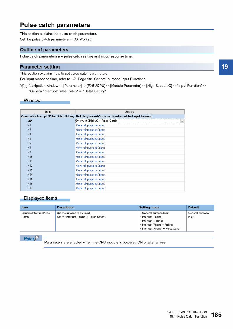
19 BUILT-IN I/O FUNCTION
19.4 Pulse Catch Function 185
19
Pulse catch parameters
This section explains the pulse catch parameters.
Set the pulse catch parameters in GX Works3.
Outline of parameters
Pulse catch parameters are pulse catch setting and input response time.
Parameter setting
This section explains how to set pulse catch parameters.
For input response time, refer to Page 191 General-purpose Input Functions.
Navigation window [Parameter] [FX5UCPU] [Module Parameter] [High Speed I/O] “Input Function"
"General/Interrupt/Pulse Catch" "Detail Setting"
Window
Displayed items
Parameters are enabled when the CPU module is powered ON or after a reset.
Item Description Setting range Default
General/Interrupt/Pulse
Catch
Set the function to be used.
Set to “Interrupt (Rising) + Pulse Catch”.
� General-purpose Input
� Interrupt (Rising)
� Interrupt (Falling)
� Interrupt (Rising + Falling)
� Interrupt (Rising) + Pulse Catch
General-purpose
Input
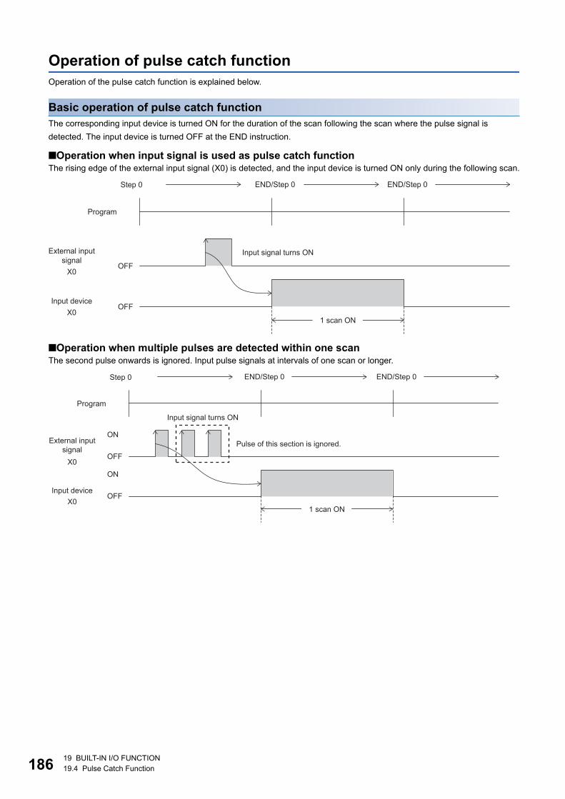
18619 BUILT-IN I/O FUNCTION
19.4 Pulse Catch Function
Operation of pulse catch function
Operation of the pulse catch function is explained below.
Basic operation of pulse catch function
The corresponding input device is turned ON for the duration of the scan following the scan where the pulse signal is
detected. The input device is turned OFF at the END instruction.
■Operation when input signal is used as pulse catch functionThe rising edge of the external input signal (X0) is detected, and the input device is turned ON only during the following scan.
■Operation when multiple pulses are detected within one scanThe second pulse onwards is ignored. Input pulse signals at intervals of one scan or longer.
Program
END/Step 0Step 0
Input signal turns ON
X0
Input device
X0
END/Step 0
OFF
OFF
1 scan ON
External input
signal
Program
END/Step 0Step 0
Input signal turns ON
X0
Input device
X0
END/Step 0
ON
ON
OFF
OFF
1 scan ON
Pulse of this section is ignored.External input
signal
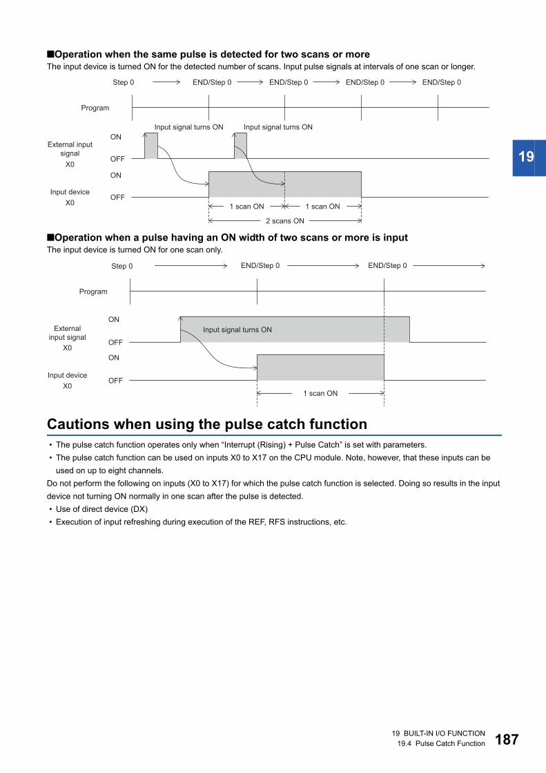
19 BUILT-IN I/O FUNCTION
19.4 Pulse Catch Function 187
19
■Operation when the same pulse is detected for two scans or moreThe input device is turned ON for the detected number of scans. Input pulse signals at intervals of one scan or longer.
■Operation when a pulse having an ON width of two scans or more is inputThe input device is turned ON for one scan only.
Cautions when using the pulse catch function
� The pulse catch function operates only when “Interrupt (Rising) + Pulse Catch” is set with parameters.
� The pulse catch function can be used on inputs X0 to X17 on the CPU module. Note, however, that these inputs can be
used on up to eight channels.
Do not perform the following on inputs (X0 to X17) for which the pulse catch function is selected. Doing so results in the input
device not turning ON normally in one scan after the pulse is detected.
� Use of direct device (DX)
� Execution of input refreshing during execution of the REF, RFS instructions, etc.
Program
END/Step 0Step 0
Input signal turns ON
X0
Input device
X0
END/Step 0
ON
ON
OFF
OFF
1 scan ON
END/Step 0 END/Step 0
Input signal turns ON
1 scan ON
2 scans ON
External input
signal
Program
END/Step 0Step 0
Input signal turns ON
X0
Input device
X0
END/Step 0
ON
ON
OFF
OFF
1 scan ON
External
input signal
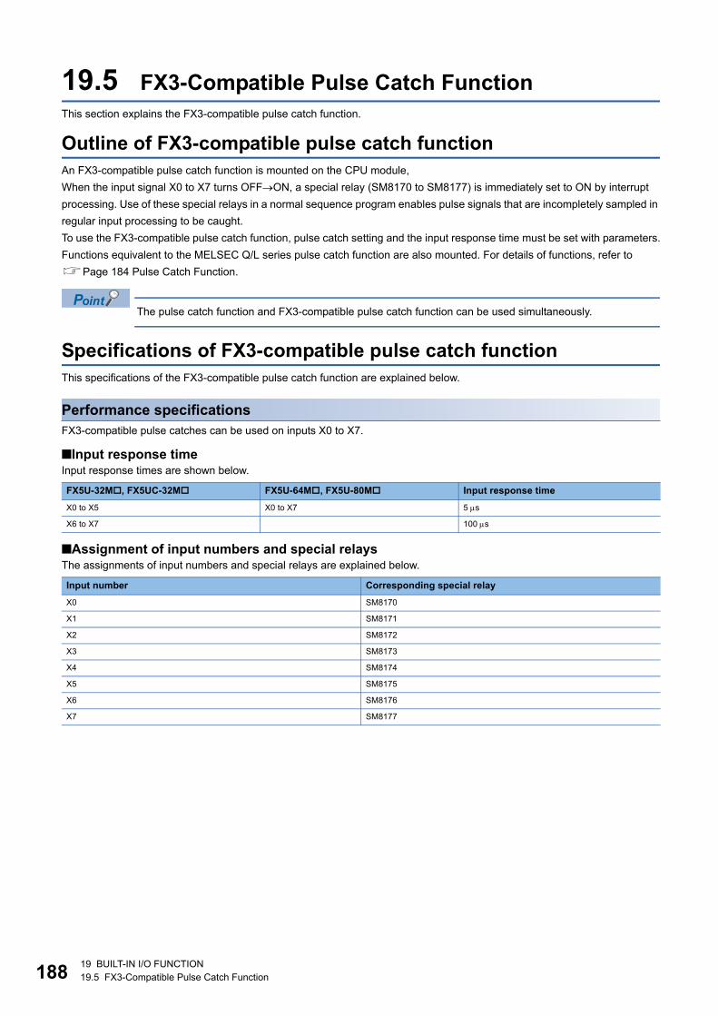
18819 BUILT-IN I/O FUNCTION
19.5 FX3-Compatible Pulse Catch Function
19.5 FX3-Compatible Pulse Catch Function
This section explains the FX3-compatible pulse catch function.
Outline of FX3-compatible pulse catch function
An FX3-compatible pulse catch function is mounted on the CPU module,
When the input signal X0 to X7 turns OFFON, a special relay (SM8170 to SM8177) is immediately set to ON by interrupt
processing. Use of these special relays in a normal sequence program enables pulse signals that are incompletely sampled in
regular input processing to be caught.
To use the FX3-compatible pulse catch function, pulse catch setting and the input response time must be set with parameters.
Functions equivalent to the MELSEC Q/L series pulse catch function are also mounted. For details of functions, refer to
Page 184 Pulse Catch Function.
The pulse catch function and FX3-compatible pulse catch function can be used simultaneously.
Specifications of FX3-compatible pulse catch function
This specifications of the FX3-compatible pulse catch function are explained below.
Performance specifications
FX3-compatible pulse catches can be used on inputs X0 to X7.
■Input response timeInput response times are shown below.
■Assignment of input numbers and special relaysThe assignments of input numbers and special relays are explained below.
FX5U-32M, FX5UC-32M FX5U-64M, FX5U-80M Input response time
X0 to X5 X0 to X7 5 s
X6 to X7 100 s
Input number Corresponding special relay
X0 SM8170
X1 SM8171
X2 SM8172
X3 SM8173
X4 SM8174
X5 SM8175
X6 SM8176
X7 SM8177
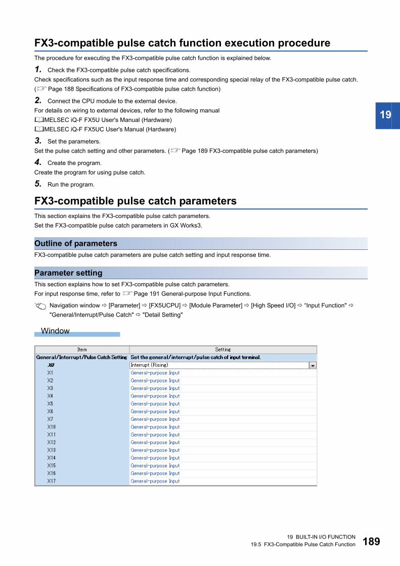
19 BUILT-IN I/O FUNCTION
19.5 FX3-Compatible Pulse Catch Function 189
19
FX3-compatible pulse catch function execution procedure
The procedure for executing the FX3-compatible pulse catch function is explained below.
1. Check the FX3-compatible pulse catch specifications.
Check specifications such as the input response time and corresponding special relay of the FX3-compatible pulse catch.
(Page 188 Specifications of FX3-compatible pulse catch function)
2. Connect the CPU module to the external device.
For details on wiring to external devices, refer to the following manual
MELSEC iQ-F FX5U User's Manual (Hardware)
MELSEC iQ-F FX5UC User's Manual (Hardware)
3. Set the parameters.
Set the pulse catch setting and other parameters. (Page 189 FX3-compatible pulse catch parameters)
4. Create the program.
Create the program for using pulse catch.
5. Run the program.
FX3-compatible pulse catch parameters
This section explains the FX3-compatible pulse catch parameters.
Set the FX3-compatible pulse catch parameters in GX Works3.
Outline of parameters
FX3-compatible pulse catch parameters are pulse catch setting and input response time.
Parameter setting
This section explains how to set FX3-compatible pulse catch parameters.
For input response time, refer to Page 191 General-purpose Input Functions.
Navigation window [Parameter] [FX5UCPU] [Module Parameter] [High Speed I/O] “Input Function"
"General/Interrupt/Pulse Catch" "Detail Setting"
Window
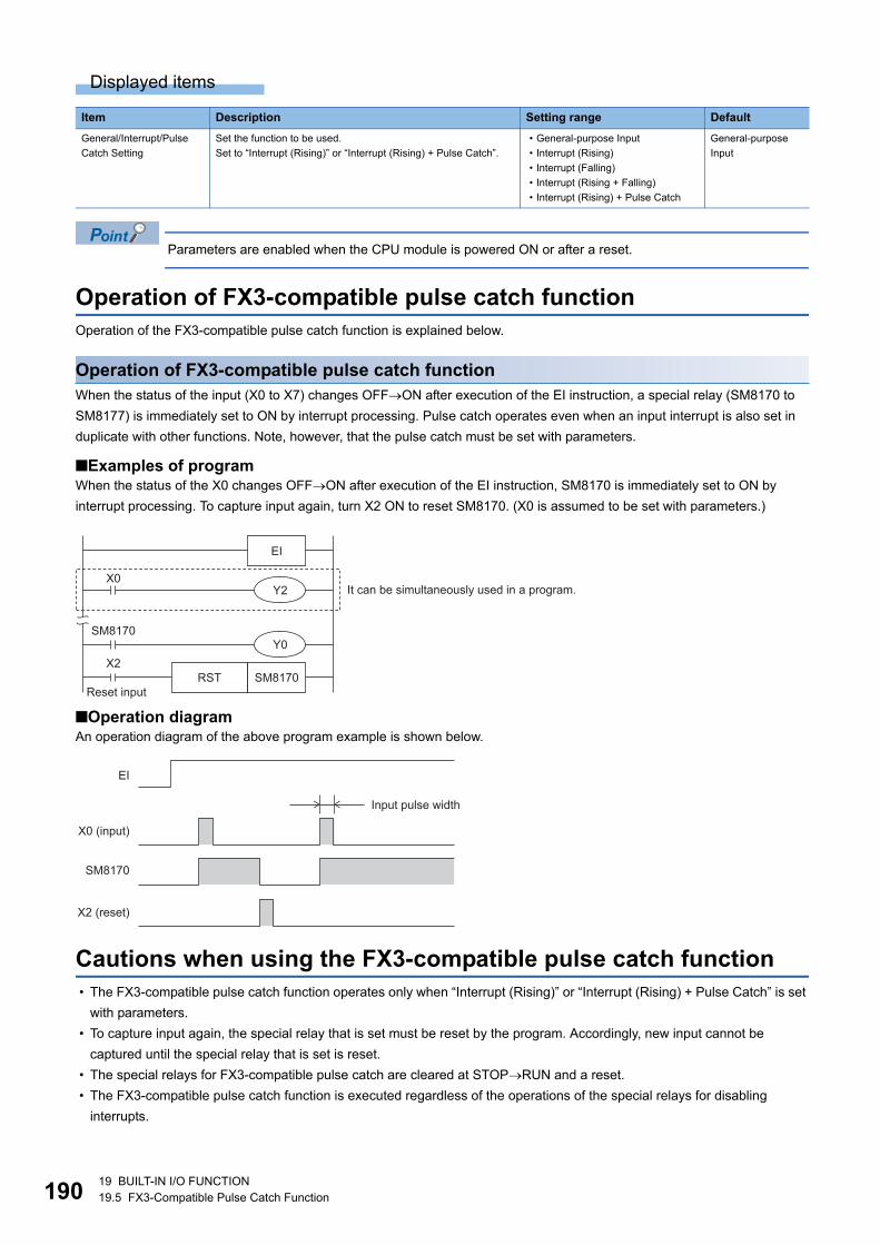
19019 BUILT-IN I/O FUNCTION
19.5 FX3-Compatible Pulse Catch Function
Displayed items
Parameters are enabled when the CPU module is powered ON or after a reset.
Operation of FX3-compatible pulse catch function
Operation of the FX3-compatible pulse catch function is explained below.
Operation of FX3-compatible pulse catch function
When the status of the input (X0 to X7) changes OFFON after execution of the EI instruction, a special relay (SM8170 to
SM8177) is immediately set to ON by interrupt processing. Pulse catch operates even when an input interrupt is also set in
duplicate with other functions. Note, however, that the pulse catch must be set with parameters.
■Examples of programWhen the status of the X0 changes OFFON after execution of the EI instruction, SM8170 is immediately set to ON by
interrupt processing. To capture input again, turn X2 ON to reset SM8170. (X0 is assumed to be set with parameters.)
■Operation diagramAn operation diagram of the above program example is shown below.
Cautions when using the FX3-compatible pulse catch function
� The FX3-compatible pulse catch function operates only when “Interrupt (Rising)” or “Interrupt (Rising) + Pulse Catch” is set
with parameters.
� To capture input again, the special relay that is set must be reset by the program. Accordingly, new input cannot be
captured until the special relay that is set is reset.
� The special relays for FX3-compatible pulse catch are cleared at STOPRUN and a reset.
� The FX3-compatible pulse catch function is executed regardless of the operations of the special relays for disabling
interrupts.
Item Description Setting range Default
General/Interrupt/Pulse
Catch Setting
Set the function to be used.
Set to “Interrupt (Rising)” or “Interrupt (Rising) + Pulse Catch”.
� General-purpose Input
� Interrupt (Rising)
� Interrupt (Falling)
� Interrupt (Rising + Falling)
� Interrupt (Rising) + Pulse Catch
General-purpose
Input
Reset input
RST
SM8170
X2
SM8170
Y0
X0Y2
EI
It can be simultaneously used in a program.
SM8170
X0 (input)
X2 (reset)
Input pulse width
EI
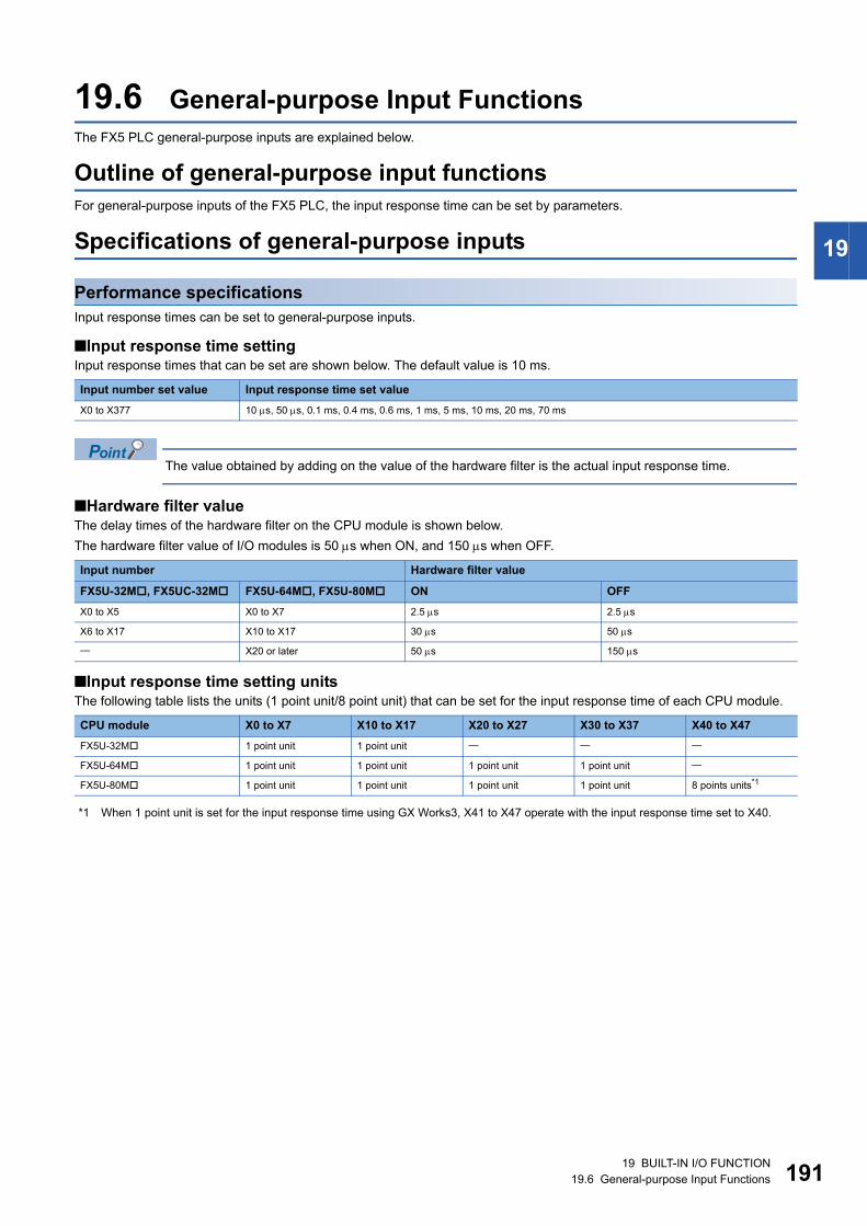
19 BUILT-IN I/O FUNCTION
19.6 General-purpose Input Functions 191
19
19.6 General-purpose Input Functions
The FX5 PLC general-purpose inputs are explained below.
Outline of general-purpose input functions
For general-purpose inputs of the FX5 PLC, the input response time can be set by parameters.
Specifications of general-purpose inputs
Performance specifications
Input response times can be set to general-purpose inputs.
■Input response time settingInput response times that can be set are shown below. The default value is 10 ms.
The value obtained by adding on the value of the hardware filter is the actual input response time.
■Hardware filter valueThe delay times of the hardware filter on the CPU module is shown below.
The hardware filter value of I/O modules is 50 s when ON, and 150 s when OFF.
■Input response time setting unitsThe following table lists the units (1 point unit/8 point unit) that can be set for the input response time of each CPU module.
*1 When 1 point unit is set for the input response time using GX Works3, X41 to X47 operate with the input response time set to X40.
Input number set value Input response time set value
X0 to X377 10 s, 50 s, 0.1 ms, 0.4 ms, 0.6 ms, 1 ms, 5 ms, 10 ms, 20 ms, 70 ms
Input number Hardware filter value
FX5U-32M, FX5UC-32M FX5U-64M, FX5U-80M ON OFF
X0 to X5 X0 to X7 2.5 s 2.5 s
X6 to X17 X10 to X17 30 s 50 s
X20 or later 50 s 150 s
CPU module X0 to X7 X10 to X17 X20 to X27 X30 to X37 X40 to X47
FX5U-32M 1 point unit 1 point unit
FX5U-64M 1 point unit 1 point unit 1 point unit 1 point unit
FX5U-80M 1 point unit 1 point unit 1 point unit 1 point unit 8 points units*1
19219 BUILT-IN I/O FUNCTION
19.6 General-purpose Input Functions
General-purpose input function parameters
This section explains the general-purpose input parameters.
Set the input response time parameters in GX Works3.
Parameter setting
This section explains how to set the input response time parameters.
Set the input response time.
Navigation window [Parameter] [FX5UCPU] [Module Parameter] [Input Response Time]
Window
Displayed items
Parameters are enabled when the CPU module is powered ON or after a reset.
Item Description Setting range Default
Response Type Select the input response time between 1 point unit and 8
point unit.
High-Speed: Unit of 1 point
Normal: Unit of 8 points
� High-Speed
� Normal
X0 to X377 Set the input response time. � No Setting
� 10micro-s (s)
� 50micro-s (s)
� 0.1ms
� 0.4ms
� 0.6ms
� 1ms
� 5ms
� 10ms
� 20ms
� 70ms
10ms
19 BUILT-IN I/O FUNCTION
19.7 PWM Function 193
19
19.7 PWM Function
This chapter explains the PWM function.
Outline of PWM output
The CPU module has a built-in PWM function, which allows PWM output on up to four channels.
For PWM output, the output channel assignment, pulse/cycle units, output pulse logic, pulse width, cycle, etc. are set using
parameters, and the HIOEN instruction is used to start/stop pulse output.
Also, the regular PWM instruction can be used.
PWM output specifications
The PWM output specifications are explained below.
Number of output channels
Up to four channels can be used for PWM output.
Output Y0 to Y7 can be selected for each channel in parameters.
Outputs (Y) assigned for PWM output in parameter settings cannot be used by the positioning function.
Pulse output performance
The cycle and pulse width are shown below.
Relationship between cycle and pulse width
The relationship between period and pulse width is shown below.
■When positive logic is setThe relationship between the period and pulse width when the output pulse logic at start of pulse output is set to "positive
logic" is shown below. (The pulse width is called the "ON width".)
� When positive logic is set, PWM output begins from output ON.)
� Pulse output is stopped at the specified number of pulses.
� Pulse output stops in the output (Y) status of before PWM output was started.
Output number Minimum period Minimum pulse width
Y0 to Y3 5 s 2 s
Y4 to Y7 400 s 200 s
Output pulse
Cycle
PWM output start
(command input)
ON width
19419 BUILT-IN I/O FUNCTION
19.7 PWM Function
■When negative logic is setThe relationship between the period and pulse width when the output pulse logic at start of pulse output is set to "negative
logic" is shown below. (The pulse width is called the "OFF width".)
� When negative logic is set, PWM output begins when the output pulse turns OFF.
� Pulse output is stopped at the specified number of pulses.
� Pulse output stops in the output (Y) status of before PWM output was started.
PWM driving method
PWM output is driven by either of the following methods.
■Driven by HIOEN instructionThe logical settings like output destination, cycle, pulse width, output pulse logic, etc. are set in parameters, and the HIOEN
instruction is used to execute pulse output. For parameters, refer to Page 195 PWM output parameters.
For the HIOEN instruction, refer to MELSEC iQ-F FX5 Programming Manual (Instructions, Standard Functions/Function
Blocks).
■Driven by PWM instructionThe PWM instruction is used to execute pulse output.
For the PWM instruction, refer to MELSEC iQ-F FX5 Programming Manual (Instructions, Standard Functions/Function
Blocks).
PWM output function execution procedure
The procedure for executing the PWM output function is explained below.
1. Check the specifications of PWM output.
Check specifications such as pulse output performance of PWM output. (Page 193 PWM output specifications)
2. Connect the CPU module to the external device.
For details on wiring to external devices, refer to the following manual
MELSEC iQ-F FX5U User's Manual (Hardware)
MELSEC iQ-F FX5UC User's Manual (Hardware)
3. Set the parameters.
Set the output destination, cycle, pulse width, output pulse logic, etc. of the PWM in parameters, (Page 195 PWM output
parameters)
4. Create the program.
Create the program for using PWM output.
5. Run the program.
Output pulseOFF width
Cycle
PWM output start
(command input)
19 BUILT-IN I/O FUNCTION
19.7 PWM Function 195
19
PWM output parameters
This section explains the PWM output parameters.
Set the PWM output parameters in GX Works3.
Outline of parameters
PWM output parameters are output destination, pulse width/cycle unit, output pulse logic, pulse width, and period.
Parameter setting
This section explains how to set the PWM output parameters.
Set the output destination, pulse width/cycle unit, output pulse logic, pulse width, period, etc. of the channel to be used.
Navigation window [Parameter] [FX5UCPU] [Module Parameter] [High Speed I/O] “Output Function"
“PWM" "Detail Setting"
Window
Displayed items
The items specified in the parameters are stored in special devices when the CPU module is set from STOP
to RUN.
Item Description Setting range Default
Use PWM Output Set whether to use PWM output or not. � Disable
� Enable
Enable
Output Signal Set the output destination device of output signal. Y0 to Y7
Pulse Width/Cycle Unit Set pulse width/cycle unit. � 1ms
� 1micro-s (s)
Output Pulse Logic Sets output pulse logic. � Positive Logic
� Negative Logic
Pulse Width Sets the ON/OFF width of the pulse. � When pulse width/period unit is set to 1 ms
1 to 2147483 ms
� When pulse width/period unit is set to 1 micro-s
(s)
1 to 2147483647 micro-s (s)
Cycle Sets cycle. � When pulse width/cycle unit is set to 1 ms
1 to 2147483 ms
� When pulse width/cycle unit is set to 1 micro-s
(s)
1 to 2147483647 micro-s (s)
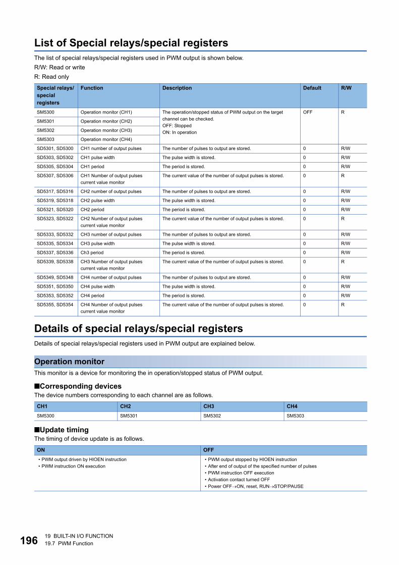
19619 BUILT-IN I/O FUNCTION
19.7 PWM Function
List of Special relays/special registers
The list of special relays/special registers used in PWM output is shown below.
R/W: Read or write
R: Read only
Details of special relays/special registers
Details of special relays/special registers used in PWM output are explained below.
Operation monitor
This monitor is a device for monitoring the in operation/stopped status of PWM output.
■Corresponding devicesThe device numbers corresponding to each channel are as follows.
■Update timingThe timing of device update is as follows.
Special relays/
special
registers
Function Description Default R/W
SM5300 Operation monitor (CH1) The operation/stopped status of PWM output on the target
channel can be checked.
OFF: Stopped
ON: In operation
OFF R
SM5301 Operation monitor (CH2)
SM5302 Operation monitor (CH3)
SM5303 Operation monitor (CH4)
SD5301, SD5300 CH1 number of output pulses The number of pulses to output are stored. 0 R/W
SD5303, SD5302 CH1 pulse width The pulse width is stored. 0 R/W
SD5305, SD5304 CH1 period The period is stored. 0 R/W
SD5307, SD5306 CH1 Number of output pulses
current value monitor
The current value of the number of output pulses is stored. 0 R
SD5317, SD5316 CH2 number of output pulses The number of pulses to output are stored. 0 R/W
SD5319, SD5318 CH2 pulse width The pulse width is stored. 0 R/W
SD5321, SD5320 CH2 period The period is stored. 0 R/W
SD5323, SD5322 CH2 Number of output pulses
current value monitor
The current value of the number of output pulses is stored. 0 R
SD5333, SD5332 CH3 number of output pulses The number of pulses to output are stored. 0 R/W
SD5335, SD5334 CH3 pulse width The pulse width is stored. 0 R/W
SD5337, SD5336 Ch3 period The period is stored. 0 R/W
SD5339, SD5338 CH3 Number of output pulses
current value monitor
The current value of the number of output pulses is stored. 0 R
SD5349, SD5348 CH4 number of output pulses The number of pulses to output are stored. 0 R/W
SD5351, SD5350 CH4 pulse width The pulse width is stored. 0 R/W
SD5353, SD5352 CH4 period The period is stored. 0 R/W
SD5355, SD5354 CH4 Number of output pulses
current value monitor
The current value of the number of output pulses is stored. 0 R
CH1 CH2 CH3 CH4
SM5300 SM5301 SM5302 SM5303
ON OFF
� PWM output driven by HIOEN instruction
� PWM instruction ON execution
� PWM output stopped by HIOEN instruction
� After end of output of the specified number of pulses
� PWM instruction OFF execution
� Activation contact turned OFF
� Power OFFON, reset, RUNSTOP/PAUSE
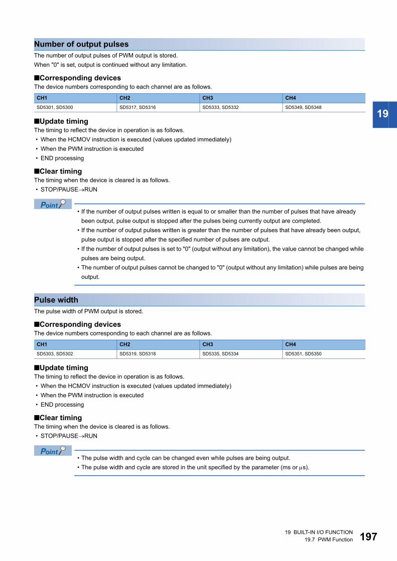
19 BUILT-IN I/O FUNCTION
19.7 PWM Function 197
19
Number of output pulses
The number of output pulses of PWM output is stored.
When "0" is set, output is continued without any limitation.
■Corresponding devicesThe device numbers corresponding to each channel are as follows.
■Update timingThe timing to reflect the device in operation is as follows.
� When the HCMOV instruction is executed (values updated immediately)
� When the PWM instruction is executed
� END processing
■Clear timingThe timing when the device is cleared is as follows.
� STOP/PAUSERUN
� If the number of output pulses written is equal to or smaller than the number of pulses that have already
been output, pulse output is stopped after the pulses being currently output are completed.
� If the number of output pulses written is greater than the number of pulses that have already been output,
pulse output is stopped after the specified number of pulses are output.
� If the number of output pulses is set to "0" (output without any limitation), the value cannot be changed while
pulses are being output.
� The number of output pulses cannot be changed to "0" (output without any limitation) while pulses are being
output.
Pulse width
The pulse width of PWM output is stored.
■Corresponding devicesThe device numbers corresponding to each channel are as follows.
■Update timingThe timing to reflect the device in operation is as follows.
� When the HCMOV instruction is executed (values updated immediately)
� When the PWM instruction is executed
� END processing
■Clear timingThe timing when the device is cleared is as follows.
� STOP/PAUSERUN
� The pulse width and cycle can be changed even while pulses are being output.
� The pulse width and cycle are stored in the unit specified by the parameter (ms or s).
CH1 CH2 CH3 CH4
SD5301, SD5300 SD5317, SD5316 SD5333, SD5332 SD5349, SD5348
CH1 CH2 CH3 CH4
SD5303, SD5302 SD5319, SD5318 SD5335, SD5334 SD5351, SD5350
19819 BUILT-IN I/O FUNCTION
19.7 PWM Function
Period
The period of PWM output is stored.
■Corresponding devicesThe device numbers corresponding to each channel are as follows.
■Update timingThe timing to reflect the device in operation is as follows.
� When the HCMOV instruction is executed (values updated immediately)
� When the PWM instruction is executed
� END processing
■Clear timingThe timing when the device is cleared is as follows.
� STOP/PAUSERUN
� The pulse width and cycle can be changed even while pulses are being output.
� The pulse width and cycle are stored in the unit specified by the parameter (ms or s).
Number of output pulses current value monitor
The current value of the number of output pulses of PWM output is stored.
■Corresponding devicesThe device numbers corresponding to each channel are as follows.
■Update timingThe timing to reflect the device in operation is as follows.
� When the HCMOV instruction is executed (values updated immediately)
� When the PWM instruction is executed
� END processing
■Clear timingThe timing when the device is cleared is as follows.
� Power OFFON
� Reset
� STOP/PAUSERUN
� If the number of output pulses is set to "0" (output without any limitation), the number of output pulse current
value monitor is fixed at "0".
� The number of output pulse current value monitor can be changed even while pulses are being output.
CH1 CH2 CH3 CH4
SD5305, SD5304 SD5321, SD5320 SD5337, SD5336 SD5353, SD5352
CH1 CH2 CH3 CH4
SD5307, SD5306 SD5323, SD5322 SD5339, SD5338 SD5355, SD5354
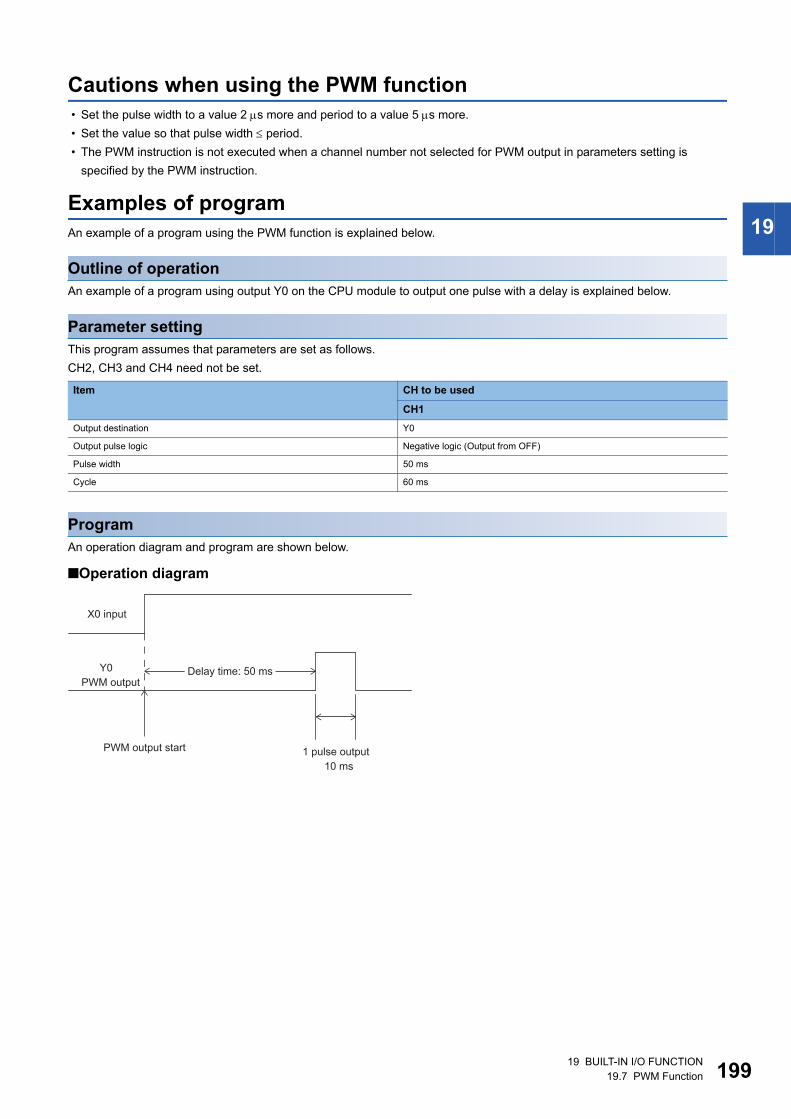
19 BUILT-IN I/O FUNCTION
19.7 PWM Function 199
19
Cautions when using the PWM function
� Set the pulse width to a value 2 s more and period to a value 5 s more.
� Set the value so that pulse width period.
� The PWM instruction is not executed when a channel number not selected for PWM output in parameters setting is
specified by the PWM instruction.
Examples of program
An example of a program using the PWM function is explained below.
Outline of operation
An example of a program using output Y0 on the CPU module to output one pulse with a delay is explained below.
Parameter setting
This program assumes that parameters are set as follows.
CH2, CH3 and CH4 need not be set.
Program
An operation diagram and program are shown below.
■Operation diagram
Item CH to be used
CH1
Output destination Y0
Output pulse logic Negative logic (Output from OFF)
Pulse width 50 ms
Cycle 60 ms
Delay time: 50 ms
1 pulse output
10 ms
X0 input
Y0
PWM output
PWM output start
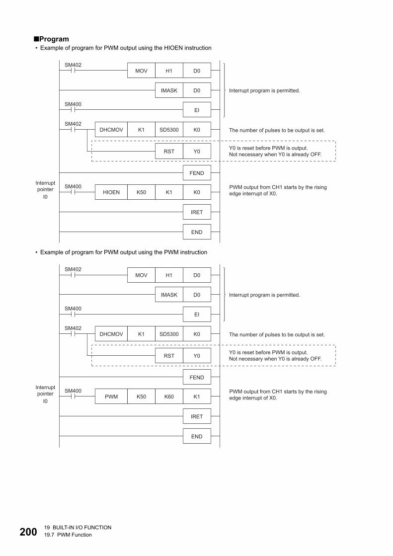
20019 BUILT-IN I/O FUNCTION
19.7 PWM Function
■Program � Example of program for PWM output using the HIOEN instruction
� Example of program for PWM output using the PWM instruction
HIOEN K0K1K50
Interrupt program is permitted.
DHCMOV K1 SD5300SM402
RST Y0
I0
SM400
FEND
K0
SM400EI
IMASK D0
MOV H1SM402
D0
IRET
END
The number of pulses to be output is set.
Y0 is reset before PWM is output.
Not necessary when Y0 is already OFF.
PWM output from CH1 starts by the rising
edge interrupt of X0.
Interrupt
pointer
PWM K1K60K50
Interrupt program is permitted.
DHCMOV K1 SD5300SM402
RST Y0
I0
SM400
FEND
K0
SM400EI
IMASK D0
MOV H1SM402
D0
IRET
END
The number of pulses to be output is set.
Y0 is reset before PWM is output.
Not necessary when Y0 is already OFF.
PWM output from CH1 starts by the rising
edge interrupt of X0.
Interrupt
pointer
20 BUILT-IN ANALOG FUNCTION
20.1 Function Outline 201
20
20 BUILT-IN ANALOG FUNCTION
The analog I/O terminal functions built into the FX5U CPU module are explained below.
20.1 Function Outline
There are two lines of analog voltage input and one line of analog voltage output built into the FX5U CPU module.
Functions must be configured using parameters to use the built-in analog circuits.
The values resulting from A/D conversion by the FX5U CPU module are automatically written in special registers for each
channel.
By setting values into the special registers in the FX5U CPU module, the signal after D/A conversion is automatically output.
For details on the function, refer to the following manual.
MELSEC iQ-F FX5 User's Manual (Analog Control)
20.2 Analog Input/Output Specifications
Analog input/output specification is shown below.
Analog input specifications
*1 "Digit" refers to digital values.
Analog output specifications
*1 There is a dead band near 0 V output, which is an area where some digital input values do not reflect analog output values.
*2 External load resistance is set to 2 k when shipped from the factory. Thus, output voltage will increase somewhat if the resistance is
set higher than 2 k. When the resistance is 1 M, output voltage increases by a maximum 2%.
*3 "Digit" refers to digital values.
Item Specifications
No. of analog input points 2 points (2 channels)
Analog input Voltage 0 to 10 V DC (input resistance 115.7 k)
Digital output Unsigned 12-bit binary
Input characteristics, max. resolution Digital output value 0 to 4000
Max. resolution 2.5 mV
Precision
(Precision for the max. digital output value)
Ambient temperature 25 5 Within 0.5% (20 digit*1)
Ambient temperature 0 to 55 Within 1.0% (40 digit*1)
Conversion speed 30 s /CH (data refreshed every operation cycle)
Absolute max. input -0.5 V, +15 V
Insulation method Inside the PLC and the analog input circuit are not insulated. Between
input terminals (channels) is not insulated.
No. of occupied input/output points 0 point (does not pertain to the max. No. of input/output points of the PLC.)
Item Specifications
No. of analog output points 1 point (1 channel)
Digital input Unsigned 12-bit binary
Analog output Voltage 0 to 10 V DC (external load resistance 2 k to 1 M)
Output characteristics, max. resolution*1 Digital input value 0 to 4000
Max. resolution 2.5 mV
Precision*2
(Precision for the max. analog output value)
Ambient temperature 25 5 Within 0.5% (20 digit*3)
Ambient temperature 0 to 55 Within 1.0% (40 digit*3)
Conversion speed 30 s (data refreshed every operation cycle)
Insulation method Inside the PLC and the analog output circuit are not insulated.
No. of occupied input/output points 0 point (does not pertain to the max. No. of input/output points of the PLC.)
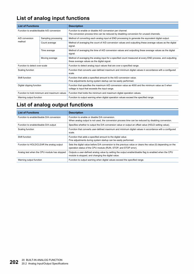
20220 BUILT-IN ANALOG FUNCTION
20.2 Analog Input/Output Specifications
List of analog input functions
List of analog output functions
List of Functions Description
Function to enable/disable A/D conversion Function to enable or disable A/D conversion per channel.
The conversion process time can be reduced by disabling conversion for unused channels.
A/D conversion
method
Sampling processing Method of converting each analog input at END processing to generate the equivalent digital output.
Count average Method of averaging the count of A/D conversion values and outputting these average values as the digital
signal.
Time average Method of averaging the time of A/D conversion values and outputting these average values as the digital
signal.
Moving average Method of averaging the analog input for a specified count measured at every END process, and outputting
these average values as the digital signal.
Function to detect over-scale Function to detect analog input values that are over a specified range.
Scaling function Function that converts user-defined maximum and minimum digital values in accordance with a configured
scale.
Shift function Function that adds a specified amount to the A/D conversion value.
Fine adjustments during system startup can be easily performed.
Digital clipping function Function that specifies the maximum A/D conversion value as 4000 and the minimum value as 0 when
voltage is input that exceeds the input range.
Function to hold minimum and maximum values Function that holds the minimum and maximum digital operation values.
Warning output function Function to output warning when digital operation values exceed the specified range.
List of Functions Description
Function to enable/disable D/A conversion Function to enable or disable D/A conversion.
When analog output is not used, the conversion process time can be reduced by disabling conversion.
Function to enable/disable D/A output Specifies whether to output the D/A conversion value or output an offset value (HOLD setting value).
Scaling function Function that converts user-defined maximum and minimum digital values in accordance with a configured
scale.
Shift function Function that adds a specified amount to the digital value.
Fine adjustments during system startup can be easily performed.
Function to HOLD/CLEAR the analog output Sets the digital value before D/A conversion to the previous value or clears the value (0) depending on the
operation status of the CPU module (RUN, STOP, and STOP error).
Analog test when the CPU module has stopped Outputs a user-defined analog value by setting the output enable/disable flag to enabled when the CPU
module is stopped, and changing the digital value.
Warning output function Function to output warning when digital values exceed the specified range.
203
PA
RT
3
PART 3 DEVICES/LABELS
This part consists of the following chapters.
21 DEVICES
22 LABELS
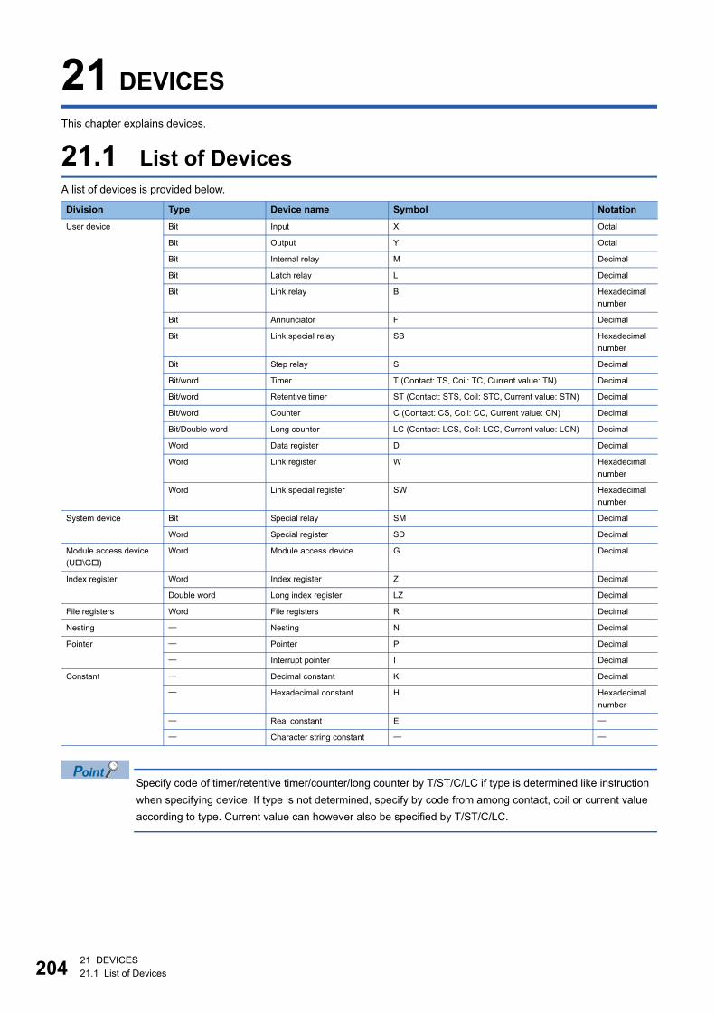
20421 DEVICES
21.1 List of Devices
21 DEVICES
This chapter explains devices.
21.1 List of Devices
A list of devices is provided below.
Specify code of timer/retentive timer/counter/long counter by T/ST/C/LC if type is determined like instruction
when specifying device. If type is not determined, specify by code from among contact, coil or current value
according to type. Current value can however also be specified by T/ST/C/LC.
Division Type Device name Symbol Notation
User device Bit Input X Octal
Bit Output Y Octal
Bit Internal relay M Decimal
Bit Latch relay L Decimal
Bit Link relay B Hexadecimal
number
Bit Annunciator F Decimal
Bit Link special relay SB Hexadecimal
number
Bit Step relay S Decimal
Bit/word Timer T (Contact: TS, Coil: TC, Current value: TN) Decimal
Bit/word Retentive timer ST (Contact: STS, Coil: STC, Current value: STN) Decimal
Bit/word Counter C (Contact: CS, Coil: CC, Current value: CN) Decimal
Bit/Double word Long counter LC (Contact: LCS, Coil: LCC, Current value: LCN) Decimal
Word Data register D Decimal
Word Link register W Hexadecimal
number
Word Link special register SW Hexadecimal
number
System device Bit Special relay SM Decimal
Word Special register SD Decimal
Module access device
(U\G)
Word Module access device G Decimal
Index register Word Index register Z Decimal
Double word Long index register LZ Decimal
File registers Word File registers R Decimal
Nesting Nesting N Decimal
Pointer Pointer P Decimal
Interrupt pointer I Decimal
Constant Decimal constant K Decimal
Hexadecimal constant H Hexadecimal
number
Real constant E
Character string constant
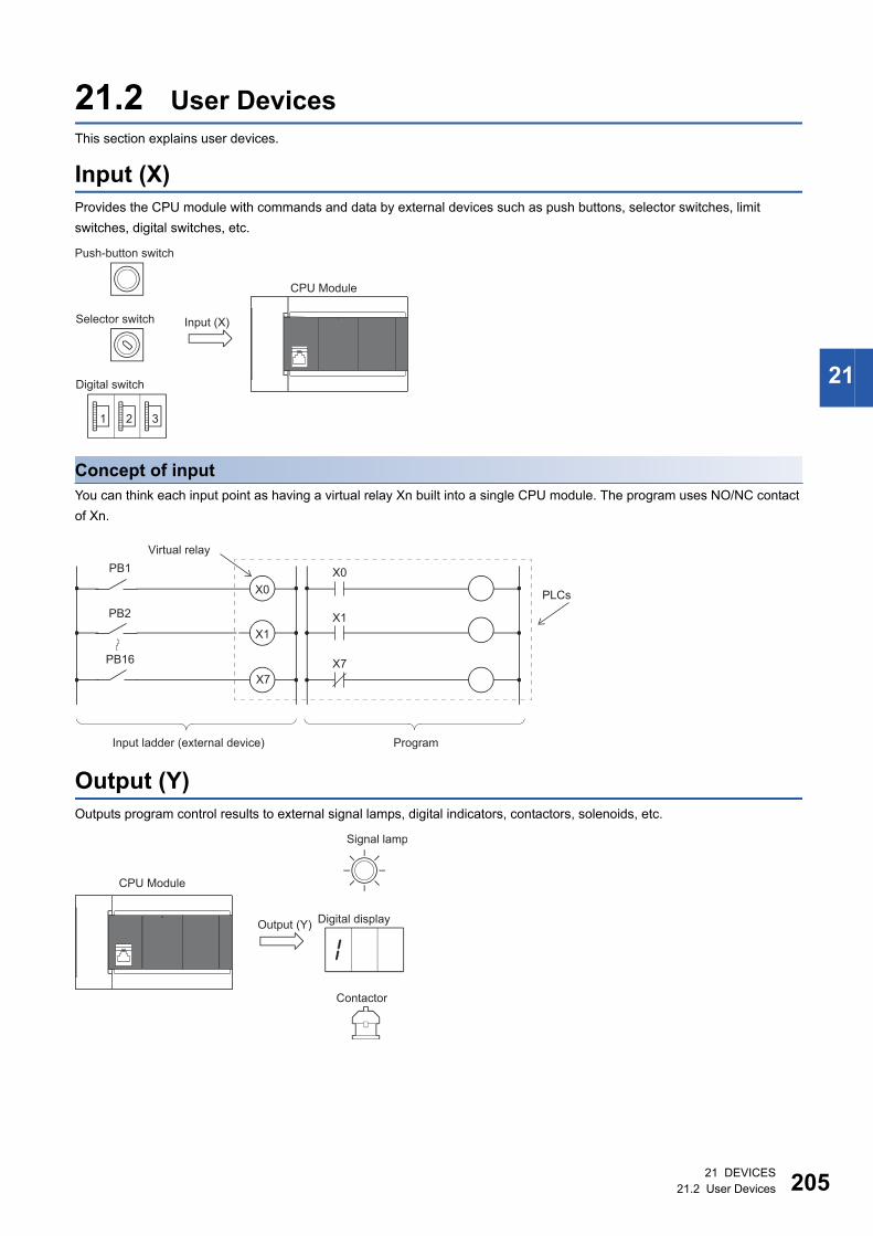
21 DEVICES
21.2 User Devices 205
21
21.2 User Devices
This section explains user devices.
Input (X)
Provides the CPU module with commands and data by external devices such as push buttons, selector switches, limit
switches, digital switches, etc.
Concept of input
You can think each input point as having a virtual relay Xn built into a single CPU module. The program uses NO/NC contact
of Xn.
Output (Y)
Outputs program control results to external signal lamps, digital indicators, contactors, solenoids, etc.
1 2 3
Push-button switch
Selector switch
Digital switch
Input (X)
CPU Module
X1
X0
X7
PB2
PB1
X0
X1
X7
PB16
Input ladder (external device) Program
PLCs
Virtual relay
CPU Module
Output (Y)
Signal lamp
Digital display
Contactor
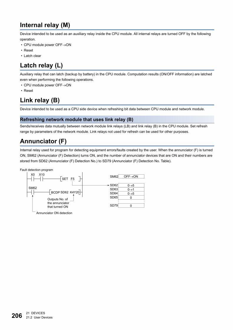
20621 DEVICES
21.2 User Devices
Internal relay (M)
Device intended to be used as an auxiliary relay inside the CPU module. All internal relays are turned OFF by the following
operation.
� CPU module power OFFON
� Reset
� Latch clear
Latch relay (L)
Auxiliary relay that can latch (backup by battery) in the CPU module. Computation results (ON/OFF information) are latched
even when performing the following operations.
� CPU module power OFFON
� Reset
Link relay (B)
Device intended to be used as a CPU side device when refreshing bit data between CPU module and network module.
Refreshing network module that uses link relay (B)
Sends/receives data mutually between network module link relays (LB) and link relay (B) in the CPU module. Set refresh
range by parameters of the network module. Link relays not used for refresh can be used for other purposes.
Annunciator (F)
Internal relay used for program for detecting equipment errors/faults created by the user. When the annunciator (F) is turned
ON, SM62 (Annunciator (F) Detection) turns ON, and the number of annunciator devices that are ON and their numbers are
stored from SD62 (Annunciator (F) Detection No.) to SD79 (Annunciator (F) Detection No. Table).
SD62BCDP
SM62
SET F5
K4Y20
X0 X10SM62
SD62
SD63
SD64
SD65
SD79
0
0
Fault detection program
Annunciator ON detection
OFFON
05
01
05
Outputs No. of
the annunciator
that turned ON
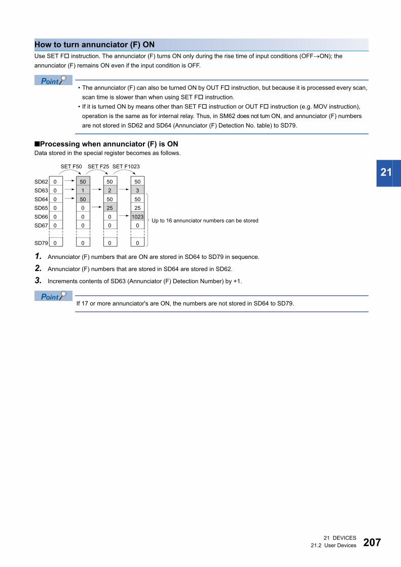
21 DEVICES
21.2 User Devices 207
21
How to turn annunciator (F) ON
Use SET F instruction. The annunciator (F) turns ON only during the rise time of input conditions (OFFON); the
annunciator (F) remains ON even if the input condition is OFF.
� The annunciator (F) can also be turned ON by OUT F instruction, but because it is processed every scan,
scan time is slower than when using SET F instruction.
� If it is turned ON by means other than SET F instruction or OUT F instruction (e.g. MOV instruction),
operation is the same as for internal relay. Thus, in SM62 does not turn ON, and annunciator (F) numbers
are not stored in SD62 and SD64 (Annunciator (F) Detection No. table) to SD79.
■Processing when annunciator (F) is ONData stored in the special register becomes as follows.
1. Annunciator (F) numbers that are ON are stored in SD64 to SD79 in sequence.
2. Annunciator (F) numbers that are stored in SD64 are stored in SD62.
3. Increments contents of SD63 (Annunciator (F) Detection Number) by +1.
If 17 or more annunciator's are ON, the numbers are not stored in SD64 to SD79.
0
0
0
0
0
0
0
SD62
SD63
SD64
SD65
SD66
SD67
SD79
50
1
50
0
0
0
0
50
2
50
25
0
0
0
50
3
50
25
1023
0
0
SET F50 SET F25 SET F1023
Up to 16 annunciator numbers can be stored
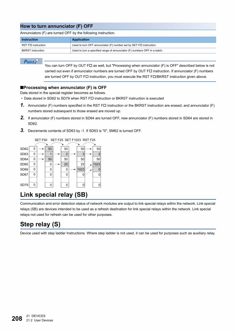
20821 DEVICES
21.2 User Devices
How to turn annunciator (F) OFF
Annunciators (F) are turned OFF by the following instruction.
You can turn OFF by OUT F as well, but "Processing when annunciator (F) is OFF" described below is not
carried out even if annunciator numbers are turned OFF by OUT F instruction. If annunciator (F) numbers
are turned OFF by OUT F instruction, you must execute the RST F/BKRST instruction given above.
■Processing when annunciator (F) is OFFData stored in the special register becomes as follows.
� Data stored in SD62 to SD79 when RST F instruction or BKRST instruction is executed
1. Annunciator (F) numbers specified in the RST F instruction or the BKRST instruction are erased, and annunciator (F)
numbers stored subsequent to those erased are moved up.
2. If annunciator (F) numbers stored in SD64 are turned OFF, new annunciator (F) numbers stored in SD64 are stored in
SD62.
3. Decrements contents of SD63 by -1. If SD63 is "0", SM62 is turned OFF.
Link special relay (SB)
Communication and error detection status of network modules are output to link special relays within the network. Link special
relays (SB) are devices intended to be used as a refresh destination for link special relays within the network. Link special
relays not used for refresh can be used for other purposes.
Step relay (S)
Device used with step ladder Instructions. Where step ladder is not used, it can be used for purposes such as auxiliary relay.
Instruction Application
RST F instruction Used to turn OFF annunciator (F) number set by SET F instruction.
BKRST instruction Used to turn a specified range of annunciator (F) numbers OFF in a batch.
0
0
0
0
0
0
0
SD62
SD63
SD64
SD65
SD66
SD67
SD79
50
1
50
0
0
0
0
50
2
50
25
0
0
0
50
3
50
25
1023
0
0
SET F50 SET F25 SET F1023
50
2
50
1023
0
0
0
RST F25
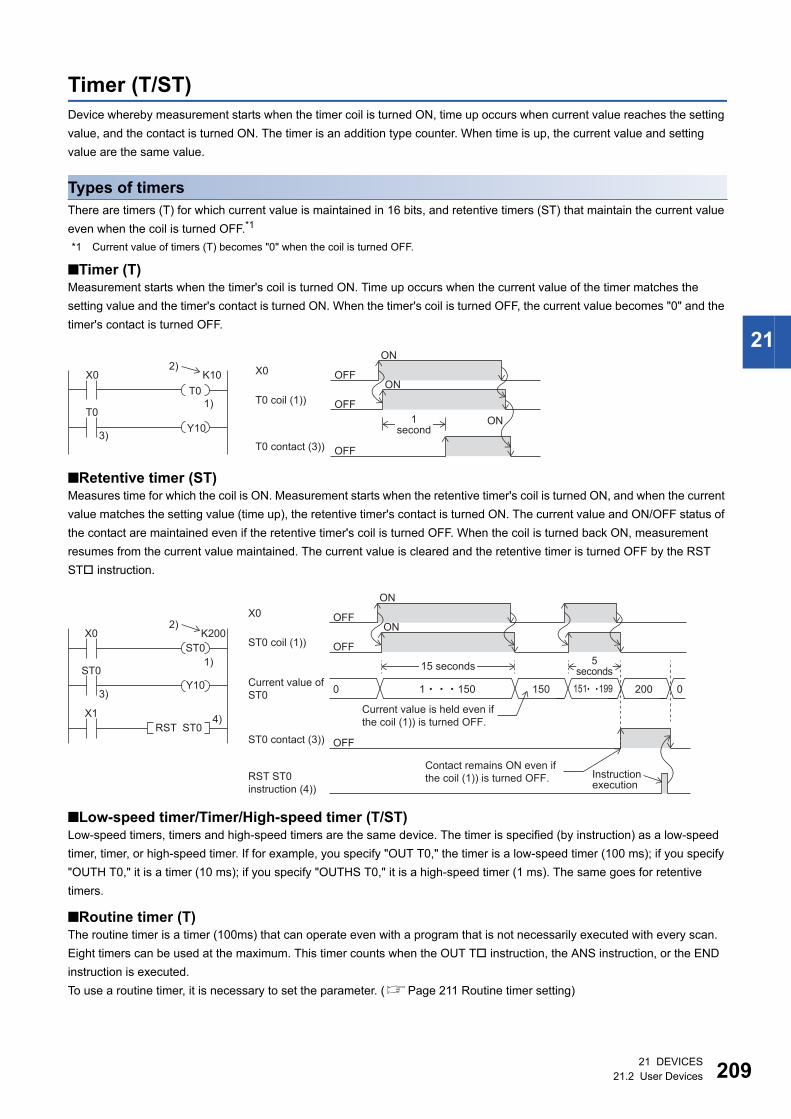
21 DEVICES
21.2 User Devices 209
21
Timer (T/ST)
Device whereby measurement starts when the timer coil is turned ON, time up occurs when current value reaches the setting
value, and the contact is turned ON. The timer is an addition type counter. When time is up, the current value and setting
value are the same value.
Types of timers
There are timers (T) for which current value is maintained in 16 bits, and retentive timers (ST) that maintain the current value
even when the coil is turned OFF.*1
*1 Current value of timers (T) becomes "0" when the coil is turned OFF.
■Timer (T)Measurement starts when the timer's coil is turned ON. Time up occurs when the current value of the timer matches the
setting value and the timer's contact is turned ON. When the timer's coil is turned OFF, the current value becomes "0" and the
timer's contact is turned OFF.
■Retentive timer (ST)Measures time for which the coil is ON. Measurement starts when the retentive timer's coil is turned ON, and when the current
value matches the setting value (time up), the retentive timer's contact is turned ON. The current value and ON/OFF status of
the contact are maintained even if the retentive timer's coil is turned OFF. When the coil is turned back ON, measurement
resumes from the current value maintained. The current value is cleared and the retentive timer is turned OFF by the RST
ST instruction.
■Low-speed timer/Timer/High-speed timer (T/ST)Low-speed timers, timers and high-speed timers are the same device. The timer is specified (by instruction) as a low-speed
timer, timer, or high-speed timer. If for example, you specify "OUT T0," the timer is a low-speed timer (100 ms); if you specify
"OUTH T0," it is a timer (10 ms); if you specify "OUTHS T0," it is a high-speed timer (1 ms). The same goes for retentive
timers.
■Routine timer (T)The routine timer is a timer (100ms) that can operate even with a program that is not necessarily executed with every scan.
Eight timers can be used at the maximum. This timer counts when the OUT T instruction, the ANS instruction, or the END
instruction is executed.
To use a routine timer, it is necessary to set the parameter. (Page 211 Routine timer setting)
Y10
T0
T0
2)X0
1)
3)
K10
OFFT0 contact (3))
ON
ON
OFFT0 coil (1))
ON
OFFX0
1second
RST ST0
X1
Y10
ST0
ST0
2)X0
1)
4)
3)
K200
0
ST0 contact (3))
ON
OFFST0 coil (1))
ON
OFFX0
5seconds
15 seconds
1 150 150 151 199 200 0
OFF
Current value is held even if
the coil (1)) is turned OFF.
Contact remains ON even if
the coil (1)) is turned OFF.
Current value of
ST0
Instruction execution
RST ST0
instruction (4))
21021 DEVICES
21.2 User Devices
Current value and measurement range of timer
■TimerThe current value range is 0 to 32767.
Timer processing method
The timer's coil is turned ON/OFF, the current value is updated and the contact is turned ON/OFF when timer's coil (OUT T
instruction) is executed.
The difference between a timer and a routine timer
Described below is the difference between a timer and a routine timer.
Precautions when using timers
Precautions when using timers are as follows.
� Do not specify the same timer coil (OUT T instruction) more than once per scan. If you do, the current value of the timer
is updated when each respective timer coil is executed, so measurement cannot be performed normally.
� If timer is not executed each scan: You cannot skip a timer coil (OUT T instruction) with the CJ instruction, etc., while the
timer's (T1 for example) coil is ON. If a timer's coil is skipped, the timer's current value is not updated, so measurement
cannot be performed normally. If a timer (T1 for example) exists within a subroutine program, be sure to execute the
subroutine coil that includes the T1 coil only once per scan while that timer's coil is ON. If not executed, measurement
cannot be performed normally.
� The timer cannot be used in the initial execution type program, fixed scan execution type program, or event execution type
program. The timer can be used in standby type programs if the coil of timer (OUT T instruction) is executed one time for
one scan using a subroutine program.
� The timer cannot be used in interrupt programs. The timer can be used in subroutine programs or FB programs if the coil of
timer (OUT T instruction) is executed one time for one scan.
� If setting value is "0": The contact is turned ON when the OUT T instruction is executed.
� If setting value is modified after time up: The timer remains in time up status and does not operate even if the setting value
is raised higher than the current value after time up.
Item Timer Routine timer
Resolution 100 ms/10 ms /1 ms 100 ms
The timing of counting (count up) When the OUT T instruction or the ANS instruction is
executed
� When the OUT T instruction or the ANS instruction is
executed
� If the OUT T instruction or the ANS instruction is not
executed, the counting starts when the END instruction
is executed.
The timing of time up (the operation at
the output contact)
When the OUT T instruction or the ANS instruction is
executed
� When the OUT T instruction or the ANS instruction is
executed
� When the END instruction is executed
Device T, ST T
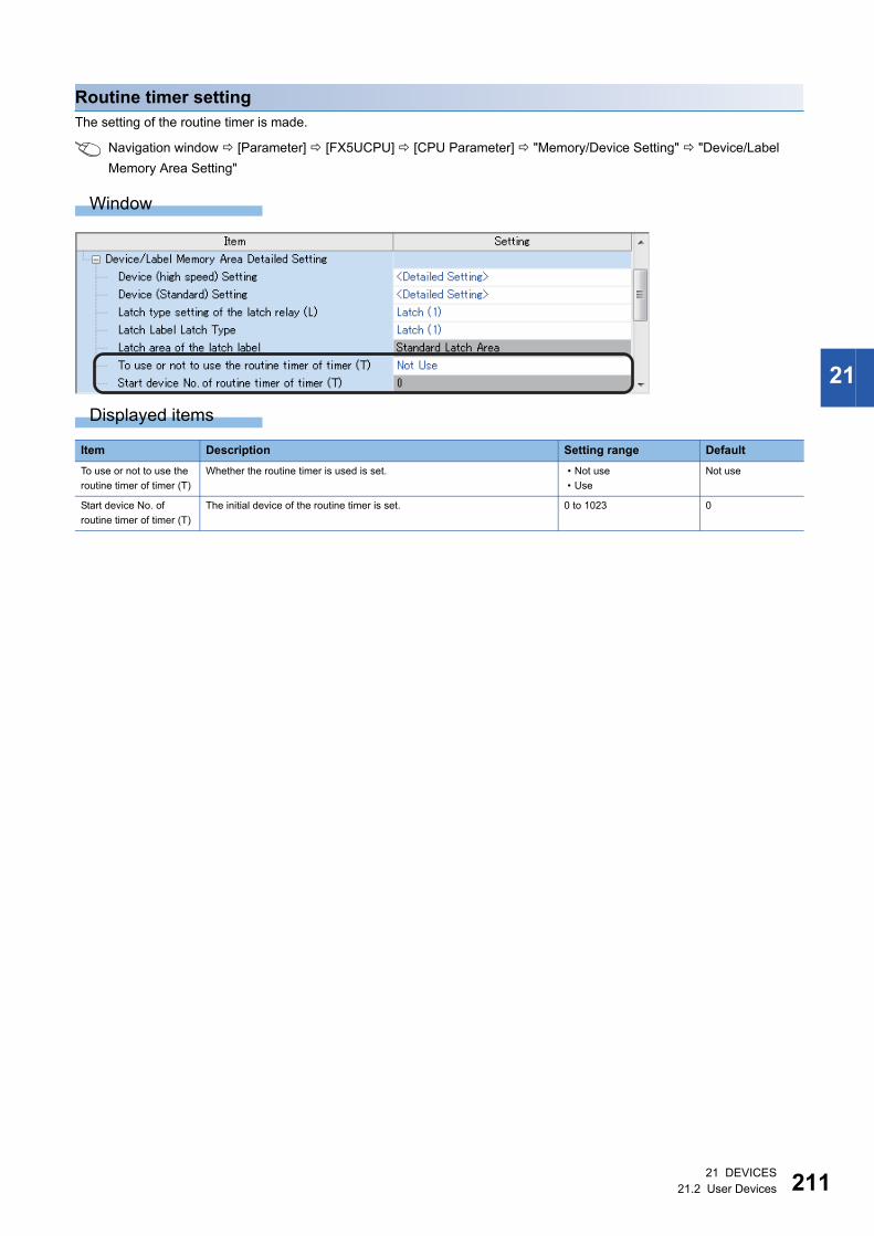
21 DEVICES
21.2 User Devices 211
21
Routine timer setting
The setting of the routine timer is made.
Navigation window [Parameter] [FX5UCPU] [CPU Parameter] "Memory/Device Setting" "Device/Label
Memory Area Setting"
Window
Displayed items
Item Description Setting range Default
To use or not to use the
routine timer of timer (T)
Whether the routine timer is used is set. � Not use
� Use
Not use
Start device No. of
routine timer of timer (T)
The initial device of the routine timer is set. 0 to 1023 0
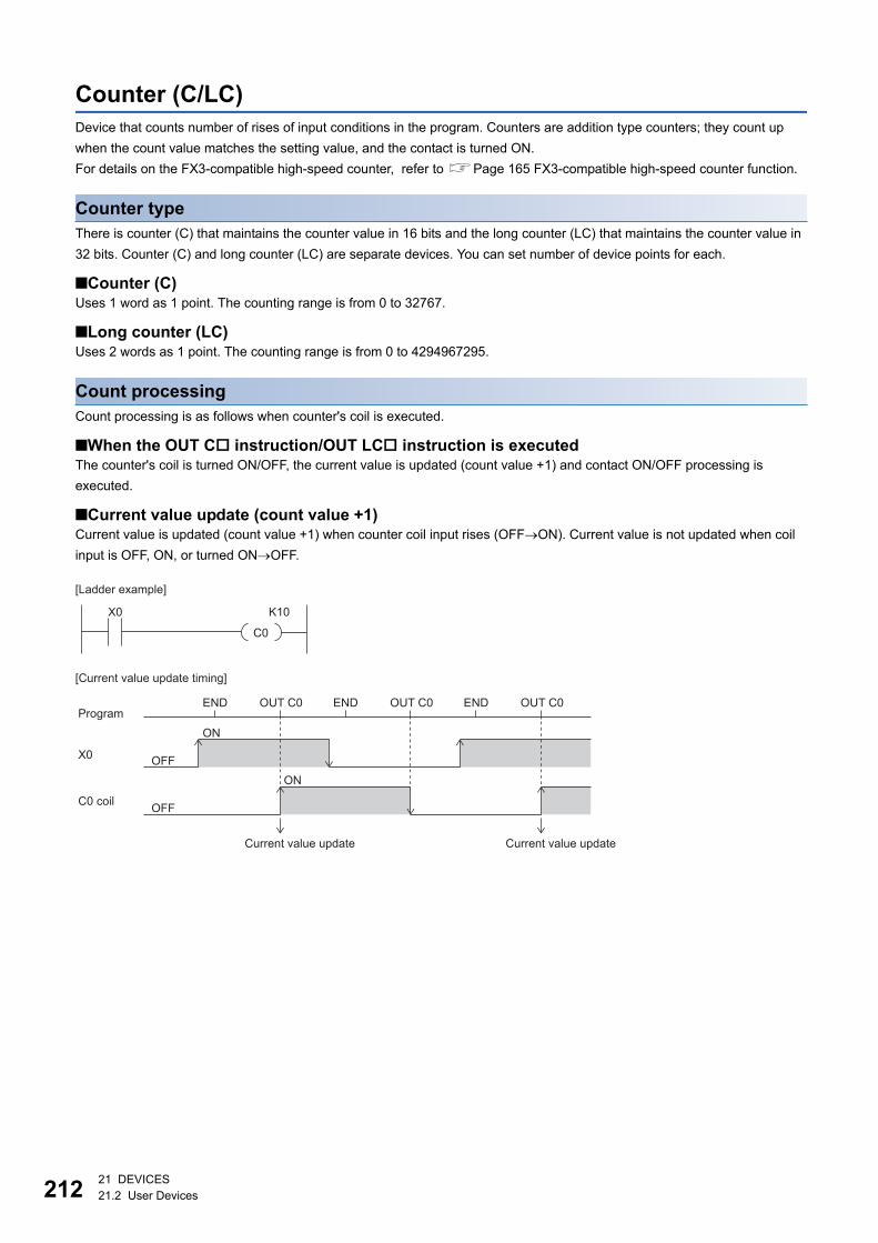
21221 DEVICES
21.2 User Devices
Counter (C/LC)
Device that counts number of rises of input conditions in the program. Counters are addition type counters; they count up
when the count value matches the setting value, and the contact is turned ON.
For details on the FX3-compatible high-speed counter, refer to Page 165 FX3-compatible high-speed counter function.
Counter type
There is counter (C) that maintains the counter value in 16 bits and the long counter (LC) that maintains the counter value in
32 bits. Counter (C) and long counter (LC) are separate devices. You can set number of device points for each.
■Counter (C)Uses 1 word as 1 point. The counting range is from 0 to 32767.
■Long counter (LC)Uses 2 words as 1 point. The counting range is from 0 to 4294967295.
Count processing
Count processing is as follows when counter's coil is executed.
■When the OUT C instruction/OUT LC instruction is executedThe counter's coil is turned ON/OFF, the current value is updated (count value +1) and contact ON/OFF processing is
executed.
■Current value update (count value +1)Current value is updated (count value +1) when counter coil input rises (OFFON). Current value is not updated when coil
input is OFF, ON, or turned ONOFF.
ON
OFF
C0
X0 K10
C0 coil
Current value updateCurrent value update
ON
END OUT C0 END OUT C0 END OUT C0
OFFX0
Program
[Current value update timing]
[Ladder example]
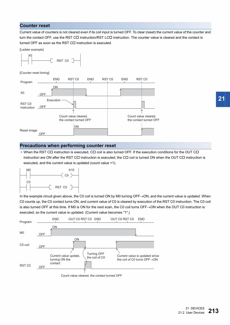
21 DEVICES
21.2 User Devices 213
21
Counter reset
Current value of counters is not cleared even if its coil input is turned OFF. To clear (reset) the current value of the counter and
turn the contact OFF, use the RST C instruction/RST LC instruction. The counter value is cleared and the contact is
turned OFF as soon as the RST C instruction is executed.
Precautions when performing counter reset
� When the RST C instruction is executed, C coil is also turned OFF. If the execution conditions for the OUT C
instruction are ON after the RST C instruction is executed, the C coil is turned ON when the OUT C instruction is
executed, and the current value is updated (count value +1).
In the example circuit given above, the C0 coil is turned ON by M0 turning OFFON, and the current value is updated. When
C0 counts up, the C0 contact turns ON, and current value of C0 is cleared by execution of the RST C0 instruction. The C0 coil
is also turned OFF at this time. If M0 is ON for the next scan, the C0 coil turns OFFON when the OUT C0 instruction is
executed, so the current value is updated. (Current value becomes "1".)
Execution
OFF
X0
ON
END RST C0 END RST C0 END RST C0
OFFX0
Program
[Counter reset timing]
[Ladder example]
RST C0
Count value cleared,
the contact turned OFF
Count value cleared,
the contact turned OFF
RST C0
instruction
ON
OFFReset image
C0
M0 K10
C0
RST C0
ON
OFF
OFFRST C0
C0 coil
ON
END RST C0OUT C0RST C0OUT C0 END END
OFFM0
Program
Current value is updated since
the coil of C0 turns OFFON
Count value cleared, the contact turned OFF
Current value update,
turning ON the
contact
Turning OFF
the coil of C0
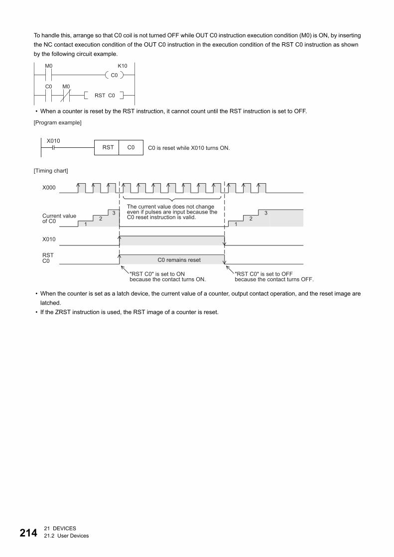
21421 DEVICES
21.2 User Devices
To handle this, arrange so that C0 coil is not turned OFF while OUT C0 instruction execution condition (M0) is ON, by inserting
the NC contact execution condition of the OUT C0 instruction in the execution condition of the RST C0 instruction as shown
by the following circuit example.
� When a counter is reset by the RST instruction, it cannot count until the RST instruction is set to OFF.
� When the counter is set as a latch device, the current value of a counter, output contact operation, and the reset image are
latched.
� If the ZRST instruction is used, the RST image of a counter is reset.
C0
M0 K10
M0C0
RST C0
X000
Current value of C0
12
3The current value does not change even if pulses are input because the C0 reset instruction is valid.
C0 remains reset
"RST C0" is set to ON because the contact turns ON.
X010
RSTC0
12
3
"RST C0" is set to OFF because the contact turns OFF.
[Timing chart]
[Program example]
X010RST C0 C0 is reset while X010 turns ON.
21 DEVICES
21.3 System Devices 215
21
Data register (D)
Device capable of storing numerical data.
Link register (W)
Device intended to be used as a CPU side device when refreshing word data between CPU module and network module.
Refreshing network module that uses link register (W)
Sends/receives data mutually between link registers (LW) in network module and link register (W) in the CPU module. Set
refresh range by parameters of the network module. Link registers not used for refresh can be used for other purposes.
Link special register (SW)
Word data such as communication and error detection status information of network modules is output to link special relays
within the network. Link special registers (SW) are devices intended to be used as a refresh destination for link special
registers within the network. Link special registers not used for refresh can be used for other purposes.
21.3 System Devices
System devices are devices for the system. Assignment/capacity are fixed and cannot be changed by the user.
Special relay (SM)
The PLC contains internal relays with fixed specifications, so it cannot be used in the program like a conventional internal
relay. It can however be turned ON/OFF to control the CPU module as needed. (Page 224 Special Relay List)
Special register (SD)
The PLC contains internal register with fixed specifications, so it cannot be used in the program like a conventional internal
register. Data, however, can be written to control the CPU module as needed. (Page 240 Special Register List)
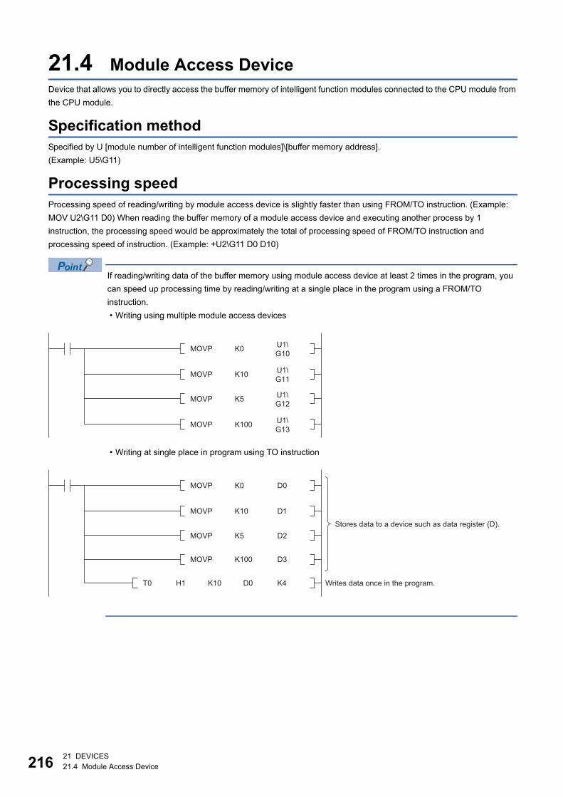
21621 DEVICES
21.4 Module Access Device
21.4 Module Access Device
Device that allows you to directly access the buffer memory of intelligent function modules connected to the CPU module from
the CPU module.
Specification method
Specified by U [module number of intelligent function modules]\[buffer memory address].
(Example: U5\G11)
Processing speed
Processing speed of reading/writing by module access device is slightly faster than using FROM/TO instruction. (Example:
MOV U2\G11 D0) When reading the buffer memory of a module access device and executing another process by 1
instruction, the processing speed would be approximately the total of processing speed of FROM/TO instruction and
processing speed of instruction. (Example: +U2\G11 D0 D10)
If reading/writing data of the buffer memory using module access device at least 2 times in the program, you
can speed up processing time by reading/writing at a single place in the program using a FROM/TO
instruction.
� Writing using multiple module access devices
� Writing at single place in program using TO instruction
MOVP K100U1\
G13
MOVP K5U1\
G12
MOVP K10U1\
G11
MOVP K0U1\
G10
K10H1T0 K4
D3MOVP K100
D2
D1
D0
D0
MOVP K5
MOVP K10
MOVP K0
Stores data to a device such as data register (D).
Writes data once in the program.
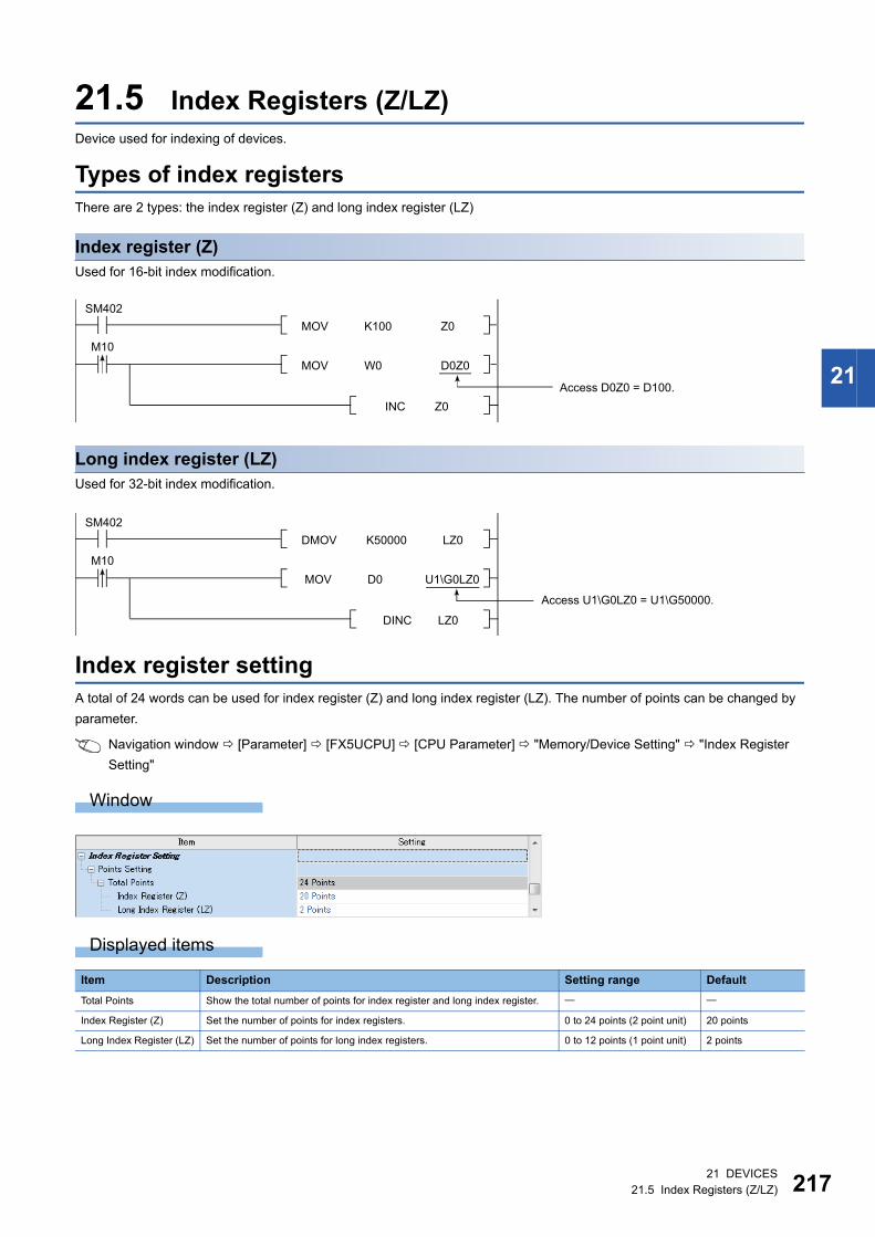
21 DEVICES
21.5 Index Registers (Z/LZ) 217
21
21.5 Index Registers (Z/LZ)
Device used for indexing of devices.
Types of index registers
There are 2 types: the index register (Z) and long index register (LZ)
Index register (Z)
Used for 16-bit index modification.
Long index register (LZ)
Used for 32-bit index modification.
Index register setting
A total of 24 words can be used for index register (Z) and long index register (LZ). The number of points can be changed by
parameter.
Navigation window [Parameter] [FX5UCPU] [CPU Parameter] "Memory/Device Setting" "Index Register
Setting"
Window
Displayed items
Item Description Setting range Default
Total Points Show the total number of points for index register and long index register.
Index Register (Z) Set the number of points for index registers. 0 to 24 points (2 point unit) 20 points
Long Index Register (LZ) Set the number of points for long index registers. 0 to 12 points (1 point unit) 2 points
MOV K100 Z0
INC Z0
MOV W0 D0Z0
SM402
M10
Access D0Z0 = D100.
DMOV K50000 LZ0
DINC LZ0
MOV D0 U1\G0LZ0
SM402
M10
Access U1\G0LZ0 = U1\G50000.
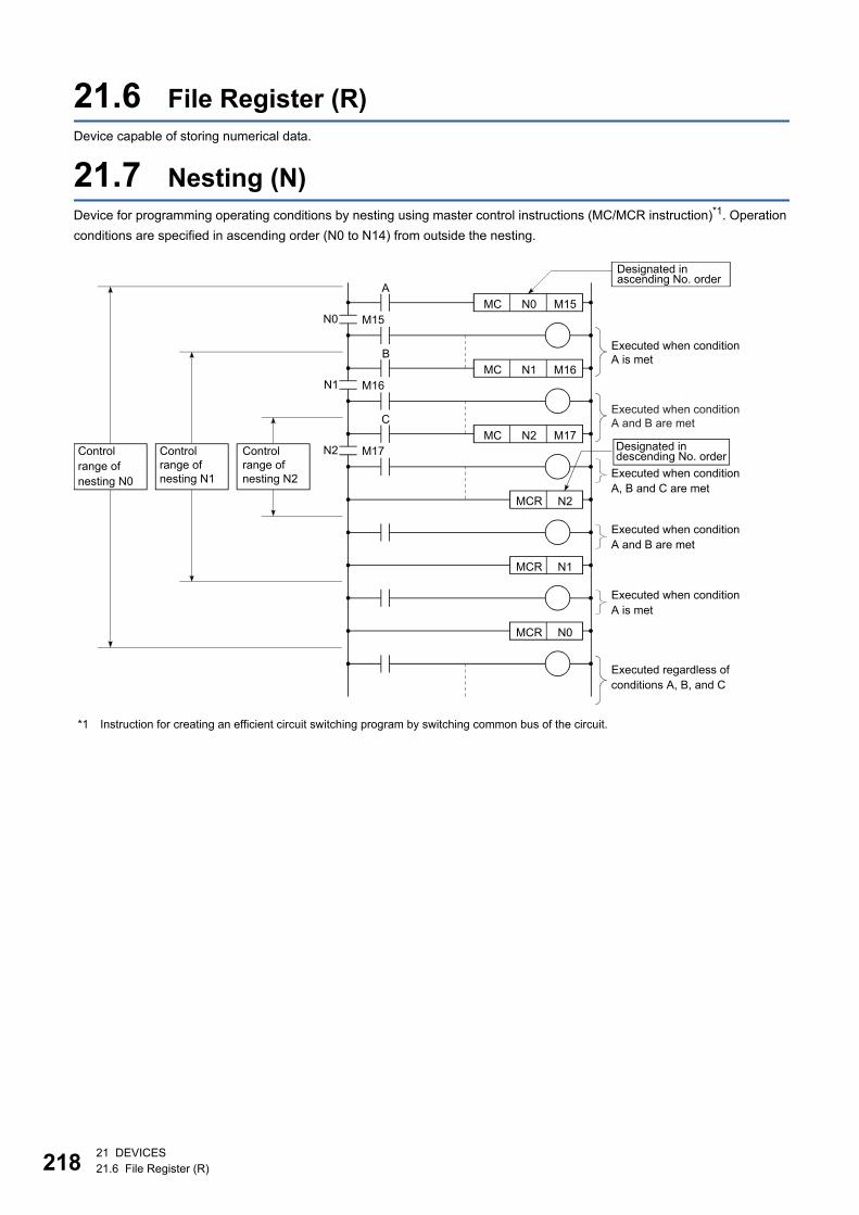
21821 DEVICES
21.6 File Register (R)
21.6 File Register (R)
Device capable of storing numerical data.
21.7 Nesting (N)
Device for programming operating conditions by nesting using master control instructions (MC/MCR instruction)*1. Operation
conditions are specified in ascending order (N0 to N14) from outside the nesting.
*1 Instruction for creating an efficient circuit switching program by switching common bus of the circuit.
M15N0
B
C
A
M15N0MC
M16N1MC
N2MCR
N1MCR
M17N2MC
N0MCR
M16N1
M17N2Control
range of
nesting N0
Control
range of
nesting N1
Control
range of
nesting N2
Designated in ascending No. order
Executed when condition
A is met
Executed when condition
A and B are met
Designated in descending No. order
Executed when condition
A, B and C are met
Executed when condition
A and B are met
Executed when condition
A is met
Executed regardless of
conditions A, B, and C
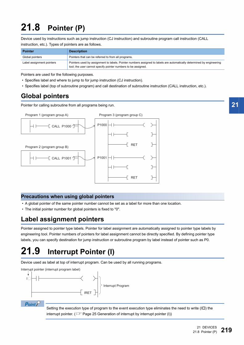
21 DEVICES
21.8 Pointer (P) 219
21
21.8 Pointer (P)
Device used by instructions such as jump instruction (CJ instruction) and subroutine program call instruction (CALL
instruction, etc.). Types of pointers are as follows.
Pointers are used for the following purposes.
� Specifies label and where to jump to for jump instruction (CJ instruction).
� Specifies label (top of subroutine program) and call destination of subroutine instruction (CALL instruction, etc.).
Global pointers
Pointer for calling subroutine from all programs being run.
Precautions when using global pointers
� A global pointer of the same pointer number cannot be set as a label for more than one location.
� The initial pointer number for global pointers is fixed to "0".
Label assignment pointers
Pointer assigned to pointer type labels. Pointer for label assignment are automatically assigned to pointer type labels by
engineering tool. Pointer numbers of pointers for label assignment cannot be directly specified. By defining pointer type
labels, you can specify destination for jump instruction or subroutine program by label instead of pointer such as P0.
21.9 Interrupt Pointer (I)
Device used as label at top of interrupt program. Can be used by all running programs.
Setting the execution type of program to the event execution type eliminates the need to write (I) the
interrupt pointer. (Page 25 Generation of interrupt by interrupt pointer (I))
Pointer Description
Global pointers Pointers that can be referred to from all programs.
Label assignment pointers Pointers used by assignment to labels. Pointer numbers assigned to labels are automatically determined by engineering
tool; the user cannot specify pointer numbers to be assigned.
Program 2 (program group B)
CALL P1001
Program 1 (program group A)
RET
RET
CALL P1000
P1001
P1000
Program 3 (program group C)
Interrupt pointer (interrupt program label)
Interrupt Program
IRET
I
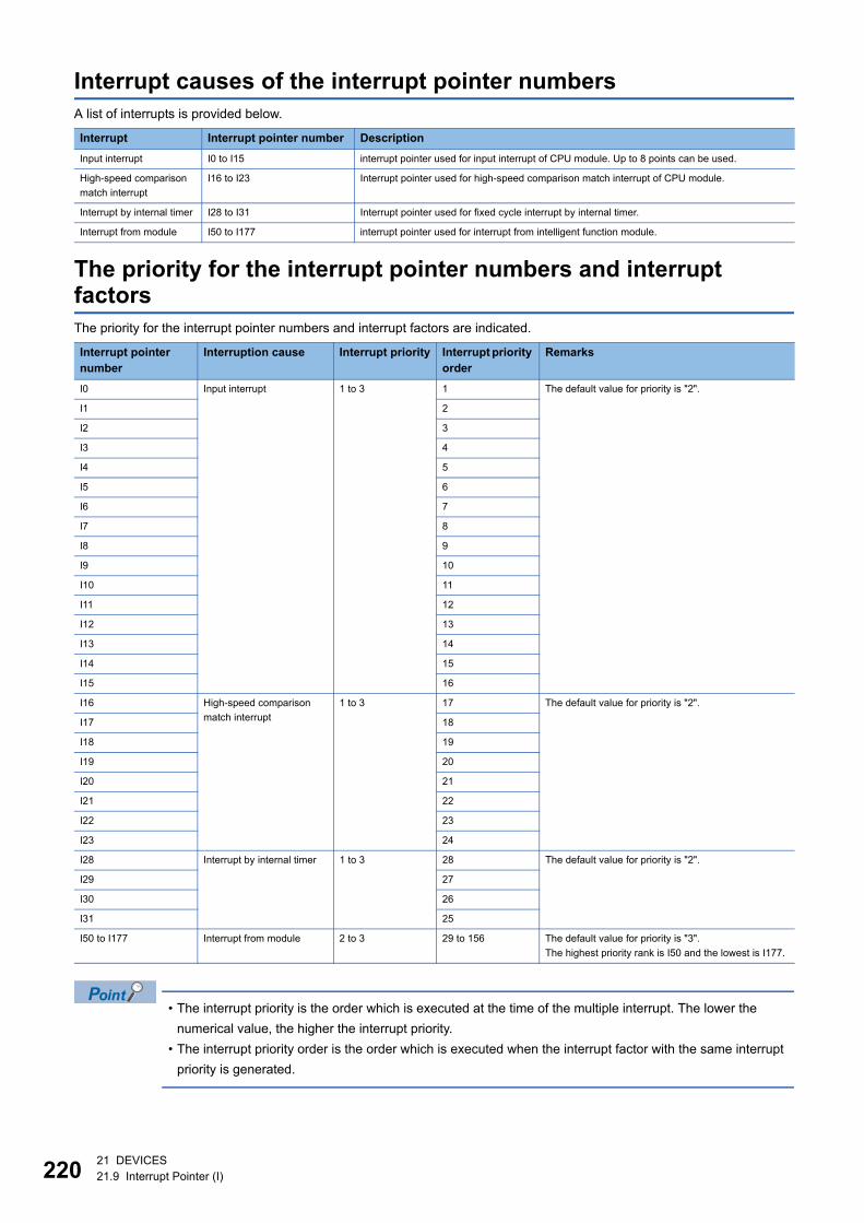
22021 DEVICES
21.9 Interrupt Pointer (I)
Interrupt causes of the interrupt pointer numbers
A list of interrupts is provided below.
The priority for the interrupt pointer numbers and interrupt factors
The priority for the interrupt pointer numbers and interrupt factors are indicated.
� The interrupt priority is the order which is executed at the time of the multiple interrupt. The lower the
numerical value, the higher the interrupt priority.
� The interrupt priority order is the order which is executed when the interrupt factor with the same interrupt
priority is generated.
Interrupt Interrupt pointer number Description
Input interrupt I0 to I15 interrupt pointer used for input interrupt of CPU module. Up to 8 points can be used.
High-speed comparison
match interrupt
I16 to I23 Interrupt pointer used for high-speed comparison match interrupt of CPU module.
Interrupt by internal timer I28 to I31 Interrupt pointer used for fixed cycle interrupt by internal timer.
Interrupt from module I50 to I177 interrupt pointer used for interrupt from intelligent function module.
Interrupt pointer
number
Interruption cause Interrupt priority Interrupt priority
order
Remarks
I0 Input interrupt 1 to 3 1 The default value for priority is "2".
I1 2
I2 3
I3 4
I4 5
I5 6
I6 7
I7 8
I8 9
I9 10
I10 11
I11 12
I12 13
I13 14
I14 15
I15 16
I16 High-speed comparison
match interrupt
1 to 3 17 The default value for priority is "2".
I17 18
I18 19
I19 20
I20 21
I21 22
I22 23
I23 24
I28 Interrupt by internal timer 1 to 3 28 The default value for priority is "2".
I29 27
I30 26
I31 25
I50 to I177 Interrupt from module 2 to 3 29 to 156 The default value for priority is "3".
The highest priority rank is I50 and the lowest is I177.
21 DEVICES
21.10 Constant 221
21
21.10 Constant
This section explains constants.
Decimal constant (K)
Device that specifies decimal data for the program. Specified by K. (Example: K1234)
The specification range is determined by type of argument data of instruction using a decimal constant.
Hexadecimal constant (H)
Device that specifies hexadecimal data for the program. Specified by H. (Example: H1234)
When specifying BCD data, specify each digit of hexadecimal number in 0 to 9. The specification range is determined by type
of argument data of instruction using a hexadecimal constant. If data size is 16 bits, H0 to HFFFF; if 32 bits, H0 to
HFFFFFFFF.
Real constant (E)
Device that specifies real numbers for the program. Specified by E. (Example: E1.234)
Setting range of real numbers
The setting range of real numbers is explained below.
-2128Device-2-126, 0, 2-126Device2128
(E-3.40282347+38 to E-1.17549435-38, 0, E1.17549435-38 to E3.40282347+38)
Operation during calculation
■Operation at overflow and underflowOperation is as follows if overflow or underflow occurs during calculation.
� Overflow: Error occurs.
� Underflow: Becomes "0" without error occurring.
■Operation when special value*1 is inputIf calculation is performed when input data is a special value, an error occurs. If "-0" occurs during calculation, it is treated as
"+0"; the calculation result does not become "-0".
*1 Special values are -0, denormalized numbers, non-numbers, .
Programming expressions
Real numbers can be specified by the following expressions.
� Normal expression: Specify a numeric value as it is. (Example: E10.2345 in the case of 10.2345)
� Scientific notation: Specify a numeric value in the format "numeric value" 10n. (Example: E1.234+3 in the case of 1234.
"+3" represents "103".)
Character string constant
Device that specifies character string. Shift JIS code character strings can be used. Character strings end with NULL
character (00H). Specify by "character string".
Argument data type of instruction Specification range of decimal constants
Data size Data type name
16 bits Word (signed) K-32768 to K32767
Word (unsigned)/Bit string (16-bit) K0 to K65535
32 bits Double word (signed) K-2147483648 to K2147483647
Double word (unsigned)/Bit string (32-bit) K0 to K4294967295
22222 LABELS
22 LABELS
Label is identifier (character string) that specifies a character string in I/O data or internal processing. When a label is used in
programming, a program can be created without being conscious about the device No.*1
*1 Label and device can be used in mixed manner.
For details on label, refer to the following.
MELSEC iQ-F FX5 Programming Manual (Program Design)

22 LABELS
223
22
MEMO
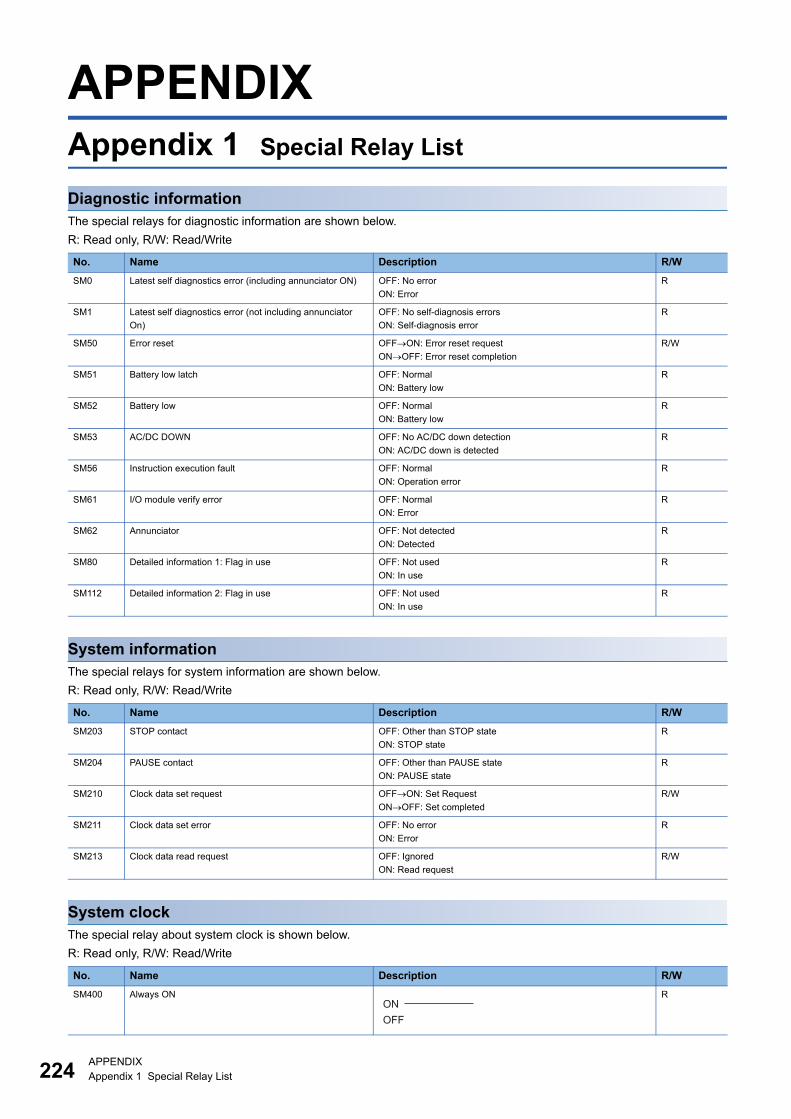
224APPENDIX
Appendix 1 Special Relay List
APPENDIXAppendix 1 Special Relay List
Diagnostic information
The special relays for diagnostic information are shown below.
R: Read only, R/W: Read/Write
System information
The special relays for system information are shown below.
R: Read only, R/W: Read/Write
System clock
The special relay about system clock is shown below.
R: Read only, R/W: Read/Write
No. Name Description R/W
SM0 Latest self diagnostics error (including annunciator ON) OFF: No error
ON: Error
R
SM1 Latest self diagnostics error (not including annunciator
On)
OFF: No self-diagnosis errors
ON: Self-diagnosis error
R
SM50 Error reset OFFON: Error reset request
ONOFF: Error reset completion
R/W
SM51 Battery low latch OFF: Normal
ON: Battery low
R
SM52 Battery low OFF: Normal
ON: Battery low
R
SM53 AC/DC DOWN OFF: No AC/DC down detection
ON: AC/DC down is detected
R
SM56 Instruction execution fault OFF: Normal
ON: Operation error
R
SM61 I/O module verify error OFF: Normal
ON: Error
R
SM62 Annunciator OFF: Not detected
ON: Detected
R
SM80 Detailed information 1: Flag in use OFF: Not used
ON: In use
R
SM112 Detailed information 2: Flag in use OFF: Not used
ON: In use
R
No. Name Description R/W
SM203 STOP contact OFF: Other than STOP state
ON: STOP state
R
SM204 PAUSE contact OFF: Other than PAUSE state
ON: PAUSE state
R
SM210 Clock data set request OFFON: Set Request
ONOFF: Set completed
R/W
SM211 Clock data set error OFF: No error
ON: Error
R
SM213 Clock data read request OFF: Ignored
ON: Read request
R/W
No. Name Description R/W
SM400 Always ON RON
OFF
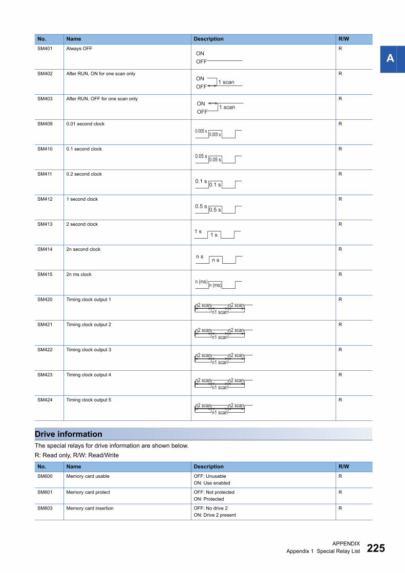
APPENDIX
Appendix 1 Special Relay List 225
A
Drive information
The special relays for drive information are shown below.
R: Read only, R/W: Read/Write
SM401 Always OFF R
SM402 After RUN, ON for one scan only R
SM403 After RUN, OFF for one scan only R
SM409 0.01 second clock R
SM410 0.1 second clock R
SM411 0.2 second clock R
SM412 1 second clock R
SM413 2 second clock R
SM414 2n second clock R
SM415 2n ms clock R
SM420 Timing clock output 1 R
SM421 Timing clock output 2 R
SM422 Timing clock output 3 R
SM423 Timing clock output 4 R
SM424 Timing clock output 5 R
No. Name Description R/W
SM600 Memory card usable OFF: Unusable
ON: Use enabled
R
SM601 Memory card protect OFF: Not protected
ON: Protected
R
SM603 Memory card insertion OFF: No drive 2
ON: Drive 2 present
R
No. Name Description R/W
ON
OFF
ON
OFF1 scan
ON
OFF1 scan
0.005 s0.005 s
0.05 s0.05 s
0.1 s0.1 s
0.5 s0.5 s
1 s1 s
n sn s
n (ms)n (ms)
n2 scann2 scan
n1 scan
n2 scann2 scan
n1 scan
n2 scann2 scan
n1 scan
n2 scann2 scan
n1 scan
n2 scann2 scan
n1 scan
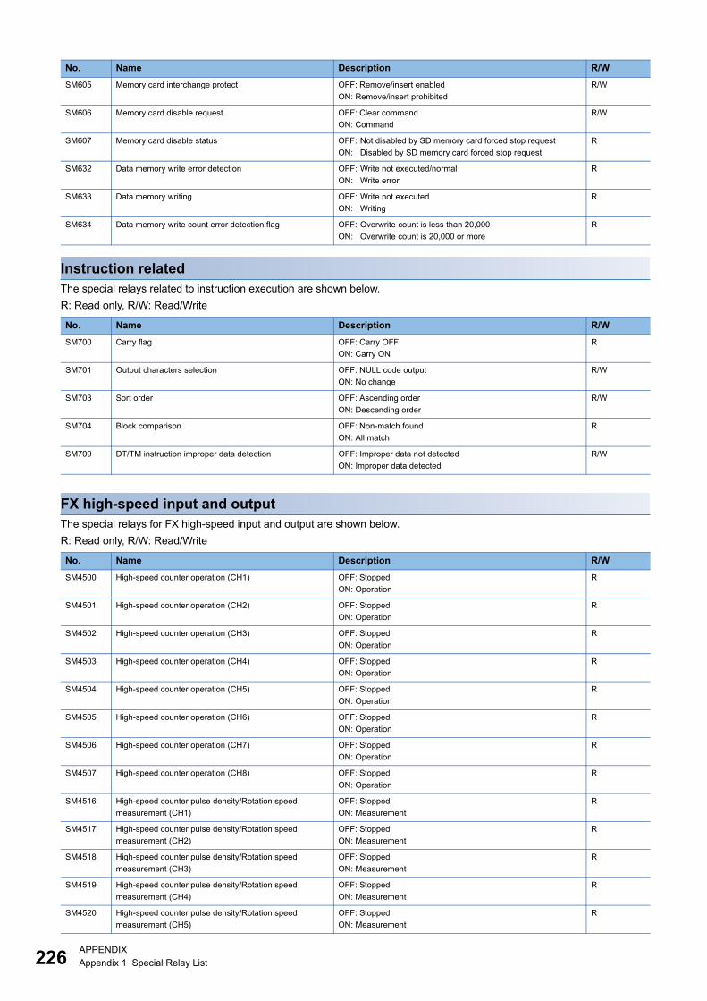
226APPENDIX
Appendix 1 Special Relay List
Instruction related
The special relays related to instruction execution are shown below.
R: Read only, R/W: Read/Write
FX high-speed input and output
The special relays for FX high-speed input and output are shown below.
R: Read only, R/W: Read/Write
SM605 Memory card interchange protect OFF: Remove/insert enabled
ON: Remove/insert prohibited
R/W
SM606 Memory card disable request OFF: Clear command
ON: Command
R/W
SM607 Memory card disable status OFF: Not disabled by SD memory card forced stop request
ON: Disabled by SD memory card forced stop request
R
SM632 Data memory write error detection OFF: Write not executed/normal
ON: Write error
R
SM633 Data memory writing OFF: Write not executed
ON: Writing
R
SM634 Data memory write count error detection flag OFF: Overwrite count is less than 20,000
ON: Overwrite count is 20,000 or more
R
No. Name Description R/W
SM700 Carry flag OFF: Carry OFF
ON: Carry ON
R
SM701 Output characters selection OFF: NULL code output
ON: No change
R/W
SM703 Sort order OFF: Ascending order
ON: Descending order
R/W
SM704 Block comparison OFF: Non-match found
ON: All match
R
SM709 DT/TM instruction improper data detection OFF: Improper data not detected
ON: Improper data detected
R/W
No. Name Description R/W
SM4500 High-speed counter operation (CH1) OFF: Stopped
ON: Operation
R
SM4501 High-speed counter operation (CH2) OFF: Stopped
ON: Operation
R
SM4502 High-speed counter operation (CH3) OFF: Stopped
ON: Operation
R
SM4503 High-speed counter operation (CH4) OFF: Stopped
ON: Operation
R
SM4504 High-speed counter operation (CH5) OFF: Stopped
ON: Operation
R
SM4505 High-speed counter operation (CH6) OFF: Stopped
ON: Operation
R
SM4506 High-speed counter operation (CH7) OFF: Stopped
ON: Operation
R
SM4507 High-speed counter operation (CH8) OFF: Stopped
ON: Operation
R
SM4516 High-speed counter pulse density/Rotation speed
measurement (CH1)
OFF: Stopped
ON: Measurement
R
SM4517 High-speed counter pulse density/Rotation speed
measurement (CH2)
OFF: Stopped
ON: Measurement
R
SM4518 High-speed counter pulse density/Rotation speed
measurement (CH3)
OFF: Stopped
ON: Measurement
R
SM4519 High-speed counter pulse density/Rotation speed
measurement (CH4)
OFF: Stopped
ON: Measurement
R
SM4520 High-speed counter pulse density/Rotation speed
measurement (CH5)
OFF: Stopped
ON: Measurement
R
No. Name Description R/W
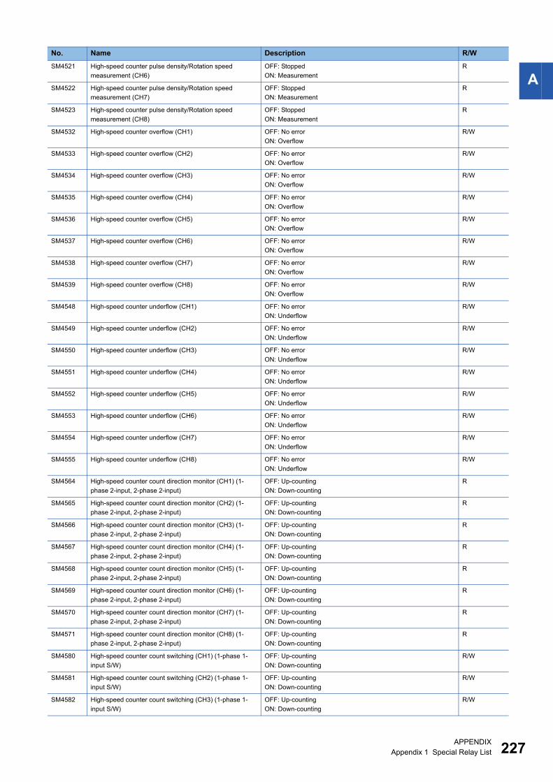
APPENDIX
Appendix 1 Special Relay List 227
ASM4521 High-speed counter pulse density/Rotation speed
measurement (CH6)
OFF: Stopped
ON: Measurement
R
SM4522 High-speed counter pulse density/Rotation speed
measurement (CH7)
OFF: Stopped
ON: Measurement
R
SM4523 High-speed counter pulse density/Rotation speed
measurement (CH8)
OFF: Stopped
ON: Measurement
R
SM4532 High-speed counter overflow (CH1) OFF: No error
ON: Overflow
R/W
SM4533 High-speed counter overflow (CH2) OFF: No error
ON: Overflow
R/W
SM4534 High-speed counter overflow (CH3) OFF: No error
ON: Overflow
R/W
SM4535 High-speed counter overflow (CH4) OFF: No error
ON: Overflow
R/W
SM4536 High-speed counter overflow (CH5) OFF: No error
ON: Overflow
R/W
SM4537 High-speed counter overflow (CH6) OFF: No error
ON: Overflow
R/W
SM4538 High-speed counter overflow (CH7) OFF: No error
ON: Overflow
R/W
SM4539 High-speed counter overflow (CH8) OFF: No error
ON: Overflow
R/W
SM4548 High-speed counter underflow (CH1) OFF: No error
ON: Underflow
R/W
SM4549 High-speed counter underflow (CH2) OFF: No error
ON: Underflow
R/W
SM4550 High-speed counter underflow (CH3) OFF: No error
ON: Underflow
R/W
SM4551 High-speed counter underflow (CH4) OFF: No error
ON: Underflow
R/W
SM4552 High-speed counter underflow (CH5) OFF: No error
ON: Underflow
R/W
SM4553 High-speed counter underflow (CH6) OFF: No error
ON: Underflow
R/W
SM4554 High-speed counter underflow (CH7) OFF: No error
ON: Underflow
R/W
SM4555 High-speed counter underflow (CH8) OFF: No error
ON: Underflow
R/W
SM4564 High-speed counter count direction monitor (CH1) (1-
phase 2-input, 2-phase 2-input)
OFF: Up-counting
ON: Down-counting
R
SM4565 High-speed counter count direction monitor (CH2) (1-
phase 2-input, 2-phase 2-input)
OFF: Up-counting
ON: Down-counting
R
SM4566 High-speed counter count direction monitor (CH3) (1-
phase 2-input, 2-phase 2-input)
OFF: Up-counting
ON: Down-counting
R
SM4567 High-speed counter count direction monitor (CH4) (1-
phase 2-input, 2-phase 2-input)
OFF: Up-counting
ON: Down-counting
R
SM4568 High-speed counter count direction monitor (CH5) (1-
phase 2-input, 2-phase 2-input)
OFF: Up-counting
ON: Down-counting
R
SM4569 High-speed counter count direction monitor (CH6) (1-
phase 2-input, 2-phase 2-input)
OFF: Up-counting
ON: Down-counting
R
SM4570 High-speed counter count direction monitor (CH7) (1-
phase 2-input, 2-phase 2-input)
OFF: Up-counting
ON: Down-counting
R
SM4571 High-speed counter count direction monitor (CH8) (1-
phase 2-input, 2-phase 2-input)
OFF: Up-counting
ON: Down-counting
R
SM4580 High-speed counter count switching (CH1) (1-phase 1-
input S/W)
OFF: Up-counting
ON: Down-counting
R/W
SM4581 High-speed counter count switching (CH2) (1-phase 1-
input S/W)
OFF: Up-counting
ON: Down-counting
R/W
SM4582 High-speed counter count switching (CH3) (1-phase 1-
input S/W)
OFF: Up-counting
ON: Down-counting
R/W
No. Name Description R/W
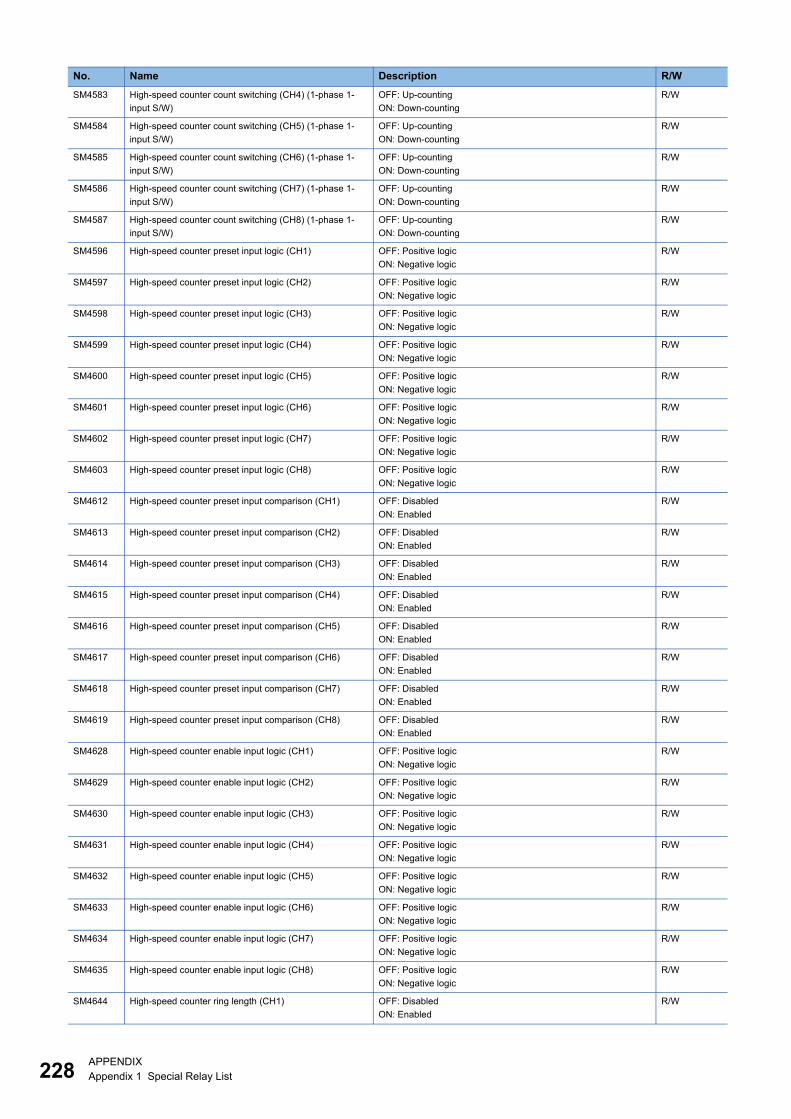
228APPENDIX
Appendix 1 Special Relay List
SM4583 High-speed counter count switching (CH4) (1-phase 1-
input S/W)
OFF: Up-counting
ON: Down-counting
R/W
SM4584 High-speed counter count switching (CH5) (1-phase 1-
input S/W)
OFF: Up-counting
ON: Down-counting
R/W
SM4585 High-speed counter count switching (CH6) (1-phase 1-
input S/W)
OFF: Up-counting
ON: Down-counting
R/W
SM4586 High-speed counter count switching (CH7) (1-phase 1-
input S/W)
OFF: Up-counting
ON: Down-counting
R/W
SM4587 High-speed counter count switching (CH8) (1-phase 1-
input S/W)
OFF: Up-counting
ON: Down-counting
R/W
SM4596 High-speed counter preset input logic (CH1) OFF: Positive logic
ON: Negative logic
R/W
SM4597 High-speed counter preset input logic (CH2) OFF: Positive logic
ON: Negative logic
R/W
SM4598 High-speed counter preset input logic (CH3) OFF: Positive logic
ON: Negative logic
R/W
SM4599 High-speed counter preset input logic (CH4) OFF: Positive logic
ON: Negative logic
R/W
SM4600 High-speed counter preset input logic (CH5) OFF: Positive logic
ON: Negative logic
R/W
SM4601 High-speed counter preset input logic (CH6) OFF: Positive logic
ON: Negative logic
R/W
SM4602 High-speed counter preset input logic (CH7) OFF: Positive logic
ON: Negative logic
R/W
SM4603 High-speed counter preset input logic (CH8) OFF: Positive logic
ON: Negative logic
R/W
SM4612 High-speed counter preset input comparison (CH1) OFF: Disabled
ON: Enabled
R/W
SM4613 High-speed counter preset input comparison (CH2) OFF: Disabled
ON: Enabled
R/W
SM4614 High-speed counter preset input comparison (CH3) OFF: Disabled
ON: Enabled
R/W
SM4615 High-speed counter preset input comparison (CH4) OFF: Disabled
ON: Enabled
R/W
SM4616 High-speed counter preset input comparison (CH5) OFF: Disabled
ON: Enabled
R/W
SM4617 High-speed counter preset input comparison (CH6) OFF: Disabled
ON: Enabled
R/W
SM4618 High-speed counter preset input comparison (CH7) OFF: Disabled
ON: Enabled
R/W
SM4619 High-speed counter preset input comparison (CH8) OFF: Disabled
ON: Enabled
R/W
SM4628 High-speed counter enable input logic (CH1) OFF: Positive logic
ON: Negative logic
R/W
SM4629 High-speed counter enable input logic (CH2) OFF: Positive logic
ON: Negative logic
R/W
SM4630 High-speed counter enable input logic (CH3) OFF: Positive logic
ON: Negative logic
R/W
SM4631 High-speed counter enable input logic (CH4) OFF: Positive logic
ON: Negative logic
R/W
SM4632 High-speed counter enable input logic (CH5) OFF: Positive logic
ON: Negative logic
R/W
SM4633 High-speed counter enable input logic (CH6) OFF: Positive logic
ON: Negative logic
R/W
SM4634 High-speed counter enable input logic (CH7) OFF: Positive logic
ON: Negative logic
R/W
SM4635 High-speed counter enable input logic (CH8) OFF: Positive logic
ON: Negative logic
R/W
SM4644 High-speed counter ring length (CH1) OFF: Disabled
ON: Enabled
R/W
No. Name Description R/W
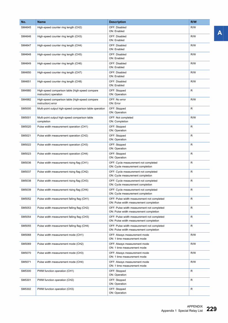
APPENDIX
Appendix 1 Special Relay List 229
ASM4645 High-speed counter ring length (CH2) OFF: Disabled
ON: Enabled
R/W
SM4646 High-speed counter ring length (CH3) OFF: Disabled
ON: Enabled
R/W
SM4647 High-speed counter ring length (CH4) OFF: Disabled
ON: Enabled
R/W
SM4648 High-speed counter ring length (CH5) OFF: Disabled
ON: Enabled
R/W
SM4649 High-speed counter ring length (CH6) OFF: Disabled
ON: Enabled
R/W
SM4650 High-speed counter ring length (CH7) OFF: Disabled
ON: Enabled
R/W
SM4651 High-speed counter ring length (CH8) OFF: Disabled
ON: Enabled
R/W
SM4980 High-speed comparison table (high-speed compare
instruction) operation
OFF: Stopped
ON: Operation
R
SM4982 High-speed comparison table (high-speed compare
instruction) error
OFF: No error
ON: Error
R/W
SM5000 Multi-point output high-speed comparison table operation OFF: Stopped
ON: Operation
R
SM5001 Multi-point output high-speed comparison table
completion
OFF: Not completed
ON: Completion
R/W
SM5020 Pulse width measurement operation (CH1) OFF: Stopped
ON: Operation
R
SM5021 Pulse width measurement operation (CH2) OFF: Stopped
ON: Operation
R
SM5022 Pulse width measurement operation (CH3) OFF: Stopped
ON: Operation
R
SM5023 Pulse width measurement operation (CH4) OFF: Stopped
ON: Operation
R
SM5036 Pulse width measurement rising flag (CH1) OFF: Cycle measurement not completed
ON: Cycle measurement completion
R
SM5037 Pulse width measurement rising flag (CH2) OFF: Cycle measurement not completed
ON: Cycle measurement completion
R
SM5038 Pulse width measurement rising flag (CH3) OFF: Cycle measurement not completed
ON: Cycle measurement completion
R
SM5039 Pulse width measurement rising flag (CH4) OFF: Cycle measurement not completed
ON: Cycle measurement completion
R
SM5052 Pulse width measurement falling flag (CH1) OFF: Pulse width measurement not completed
ON: Pulse width measurement completion
R
SM5053 Pulse width measurement falling flag (CH2) OFF: Pulse width measurement not completed
ON: Pulse width measurement completion
R
SM5054 Pulse width measurement falling flag (CH3) OFF: Pulse width measurement not completed
ON: Pulse width measurement completion
R
SM5055 Pulse width measurement falling flag (CH4) OFF: Pulse width measurement not completed
ON: Pulse width measurement completion
R
SM5068 Pulse width measurement mode (CH1) OFF: Always measurement mode
ON: 1 time measurement mode
R/W
SM5069 Pulse width measurement mode (CH2) OFF: Always measurement mode
ON: 1 time measurement mode
R/W
SM5070 Pulse width measurement mode (CH3) OFF: Always measurement mode
ON: 1 time measurement mode
R/W
SM5071 Pulse width measurement mode (CH4) OFF: Always measurement mode
ON: 1 time measurement mode
R/W
SM5300 PWM function operation (CH1) OFF: Stopped
ON: Operation
R
SM5301 PWM function operation (CH2) OFF: Stopped
ON: Operation
R
SM5302 PWM function operation (CH3) OFF: Stopped
ON: Operation
R
No. Name Description R/W
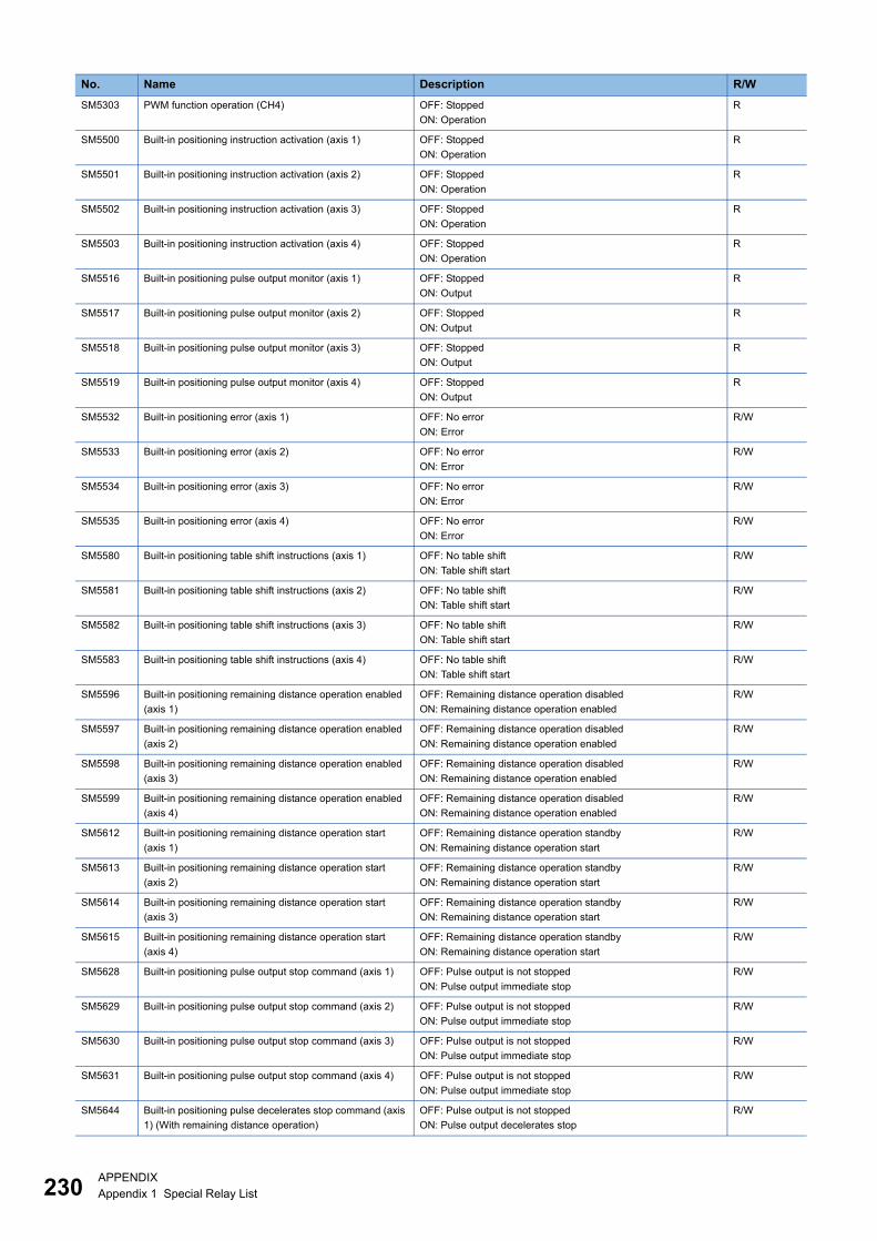
230APPENDIX
Appendix 1 Special Relay List
SM5303 PWM function operation (CH4) OFF: Stopped
ON: Operation
R
SM5500 Built-in positioning instruction activation (axis 1) OFF: Stopped
ON: Operation
R
SM5501 Built-in positioning instruction activation (axis 2) OFF: Stopped
ON: Operation
R
SM5502 Built-in positioning instruction activation (axis 3) OFF: Stopped
ON: Operation
R
SM5503 Built-in positioning instruction activation (axis 4) OFF: Stopped
ON: Operation
R
SM5516 Built-in positioning pulse output monitor (axis 1) OFF: Stopped
ON: Output
R
SM5517 Built-in positioning pulse output monitor (axis 2) OFF: Stopped
ON: Output
R
SM5518 Built-in positioning pulse output monitor (axis 3) OFF: Stopped
ON: Output
R
SM5519 Built-in positioning pulse output monitor (axis 4) OFF: Stopped
ON: Output
R
SM5532 Built-in positioning error (axis 1) OFF: No error
ON: Error
R/W
SM5533 Built-in positioning error (axis 2) OFF: No error
ON: Error
R/W
SM5534 Built-in positioning error (axis 3) OFF: No error
ON: Error
R/W
SM5535 Built-in positioning error (axis 4) OFF: No error
ON: Error
R/W
SM5580 Built-in positioning table shift instructions (axis 1) OFF: No table shift
ON: Table shift start
R/W
SM5581 Built-in positioning table shift instructions (axis 2) OFF: No table shift
ON: Table shift start
R/W
SM5582 Built-in positioning table shift instructions (axis 3) OFF: No table shift
ON: Table shift start
R/W
SM5583 Built-in positioning table shift instructions (axis 4) OFF: No table shift
ON: Table shift start
R/W
SM5596 Built-in positioning remaining distance operation enabled
(axis 1)
OFF: Remaining distance operation disabled
ON: Remaining distance operation enabled
R/W
SM5597 Built-in positioning remaining distance operation enabled
(axis 2)
OFF: Remaining distance operation disabled
ON: Remaining distance operation enabled
R/W
SM5598 Built-in positioning remaining distance operation enabled
(axis 3)
OFF: Remaining distance operation disabled
ON: Remaining distance operation enabled
R/W
SM5599 Built-in positioning remaining distance operation enabled
(axis 4)
OFF: Remaining distance operation disabled
ON: Remaining distance operation enabled
R/W
SM5612 Built-in positioning remaining distance operation start
(axis 1)
OFF: Remaining distance operation standby
ON: Remaining distance operation start
R/W
SM5613 Built-in positioning remaining distance operation start
(axis 2)
OFF: Remaining distance operation standby
ON: Remaining distance operation start
R/W
SM5614 Built-in positioning remaining distance operation start
(axis 3)
OFF: Remaining distance operation standby
ON: Remaining distance operation start
R/W
SM5615 Built-in positioning remaining distance operation start
(axis 4)
OFF: Remaining distance operation standby
ON: Remaining distance operation start
R/W
SM5628 Built-in positioning pulse output stop command (axis 1) OFF: Pulse output is not stopped
ON: Pulse output immediate stop
R/W
SM5629 Built-in positioning pulse output stop command (axis 2) OFF: Pulse output is not stopped
ON: Pulse output immediate stop
R/W
SM5630 Built-in positioning pulse output stop command (axis 3) OFF: Pulse output is not stopped
ON: Pulse output immediate stop
R/W
SM5631 Built-in positioning pulse output stop command (axis 4) OFF: Pulse output is not stopped
ON: Pulse output immediate stop
R/W
SM5644 Built-in positioning pulse decelerates stop command (axis
1) (With remaining distance operation)
OFF: Pulse output is not stopped
ON: Pulse output decelerates stop
R/W
No. Name Description R/W
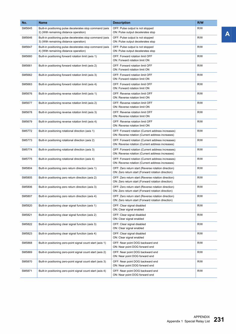
APPENDIX
Appendix 1 Special Relay List 231
ASM5645 Built-in positioning pulse decelerates stop command (axis
2) (With remaining distance operation)
OFF: Pulse output is not stopped
ON: Pulse output decelerates stop
R/W
SM5646 Built-in positioning pulse decelerates stop command (axis
3) (With remaining distance operation)
OFF: Pulse output is not stopped
ON: Pulse output decelerates stop
R/W
SM5647 Built-in positioning pulse decelerates stop command (axis
4) (With remaining distance operation)
OFF: Pulse output is not stopped
ON: Pulse output decelerates stop
R/W
SM5660 Built-in positioning forward rotation limit (axis 1) OFF: Forward rotation limit OFF
ON: Forward rotation limit ON
R/W
SM5661 Built-in positioning forward rotation limit (axis 2) OFF: Forward rotation limit OFF
ON: Forward rotation limit ON
R/W
SM5662 Built-in positioning forward rotation limit (axis 3) OFF: Forward rotation limit OFF
ON: Forward rotation limit ON
R/W
SM5663 Built-in positioning forward rotation limit (axis 4) OFF: Forward rotation limit OFF
ON: Forward rotation limit ON
R/W
SM5676 Built-in positioning reverse rotation limit (axis 1) OFF: Reverse rotation limit OFF
ON: Reverse rotation limit ON
R/W
SM5677 Built-in positioning reverse rotation limit (axis 2) OFF: Reverse rotation limit OFF
ON: Reverse rotation limit ON
R/W
SM5678 Built-in positioning reverse rotation limit (axis 3) OFF: Reverse rotation limit OFF
ON: Reverse rotation limit ON
R/W
SM5679 Built-in positioning reverse rotation limit (axis 4) OFF: Reverse rotation limit OFF
ON: Reverse rotation limit ON
R/W
SM5772 Built-in positioning rotational direction (axis 1) OFF: Forward rotation (Current address increases)
ON: Reverse rotation (Current address increases)
R/W
SM5773 Built-in positioning rotational direction (axis 2) OFF: Forward rotation (Current address increases)
ON: Reverse rotation (Current address increases)
R/W
SM5774 Built-in positioning rotational direction (axis 3) OFF: Forward rotation (Current address increases)
ON: Reverse rotation (Current address increases)
R/W
SM5775 Built-in positioning rotational direction (axis 4) OFF: Forward rotation (Current address increases)
ON: Reverse rotation (Current address increases)
R/W
SM5804 Built-in positioning zero return direction (axis 1) OFF: Zero return start (Reverse rotation direction)
ON: Zero return start (Forward rotation direction)
R/W
SM5805 Built-in positioning zero return direction (axis 2) OFF: Zero return start (Reverse rotation direction)
ON: Zero return start (Forward rotation direction)
R/W
SM5806 Built-in positioning zero return direction (axis 3) OFF: Zero return start (Reverse rotation direction)
ON: Zero return start (Forward rotation direction)
R/W
SM5807 Built-in positioning zero return direction (axis 4) OFF: Zero return start (Reverse rotation direction)
ON: Zero return start (Forward rotation direction)
R/W
SM5820 Built-in positioning clear signal function (axis 1) OFF: Clear signal disabled
ON: Clear signal enabled
R/W
SM5821 Built-in positioning clear signal function (axis 2) OFF: Clear signal disabled
ON: Clear signal enabled
R/W
SM5822 Built-in positioning clear signal function (axis 3) OFF: Clear signal disabled
ON: Clear signal enabled
R/W
SM5823 Built-in positioning clear signal function (axis 4) OFF: Clear signal disabled
ON: Clear signal enabled
R/W
SM5868 Built-in positioning zero-point signal count start (axis 1) OFF: Near point DOG backward end
ON: Near point DOG forward end
R/W
SM5869 Built-in positioning zero-point signal count start (axis 2) OFF: Near point DOG backward end
ON: Near point DOG forward end
R/W
SM5870 Built-in positioning zero-point signal count start (axis 3) OFF: Near point DOG backward end
ON: Near point DOG forward end
R/W
SM5871 Built-in positioning zero-point signal count start (axis 4) OFF: Near point DOG backward end
ON: Near point DOG forward end
R/W
No. Name Description R/W
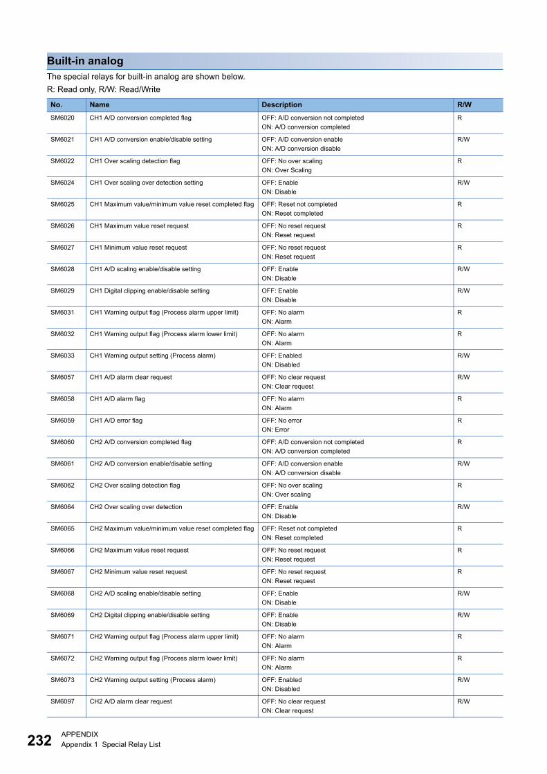
232APPENDIX
Appendix 1 Special Relay List
Built-in analog
The special relays for built-in analog are shown below.
R: Read only, R/W: Read/Write
No. Name Description R/W
SM6020 CH1 A/D conversion completed flag OFF: A/D conversion not completed
ON: A/D conversion completed
R
SM6021 CH1 A/D conversion enable/disable setting OFF: A/D conversion enable
ON: A/D conversion disable
R/W
SM6022 CH1 Over scaling detection flag OFF: No over scaling
ON: Over Scaling
R
SM6024 CH1 Over scaling over detection setting OFF: Enable
ON: Disable
R/W
SM6025 CH1 Maximum value/minimum value reset completed flag OFF: Reset not completed
ON: Reset completed
R
SM6026 CH1 Maximum value reset request OFF: No reset request
ON: Reset request
R
SM6027 CH1 Minimum value reset request OFF: No reset request
ON: Reset request
R
SM6028 CH1 A/D scaling enable/disable setting OFF: Enable
ON: Disable
R/W
SM6029 CH1 Digital clipping enable/disable setting OFF: Enable
ON: Disable
R/W
SM6031 CH1 Warning output flag (Process alarm upper limit) OFF: No alarm
ON: Alarm
R
SM6032 CH1 Warning output flag (Process alarm lower limit) OFF: No alarm
ON: Alarm
R
SM6033 CH1 Warning output setting (Process alarm) OFF: Enabled
ON: Disabled
R/W
SM6057 CH1 A/D alarm clear request OFF: No clear request
ON: Clear request
R/W
SM6058 CH1 A/D alarm flag OFF: No alarm
ON: Alarm
R
SM6059 CH1 A/D error flag OFF: No error
ON: Error
R
SM6060 CH2 A/D conversion completed flag OFF: A/D conversion not completed
ON: A/D conversion completed
R
SM6061 CH2 A/D conversion enable/disable setting OFF: A/D conversion enable
ON: A/D conversion disable
R/W
SM6062 CH2 Over scaling detection flag OFF: No over scaling
ON: Over scaling
R
SM6064 CH2 Over scaling over detection OFF: Enable
ON: Disable
R/W
SM6065 CH2 Maximum value/minimum value reset completed flag OFF: Reset not completed
ON: Reset completed
R
SM6066 CH2 Maximum value reset request OFF: No reset request
ON: Reset request
R
SM6067 CH2 Minimum value reset request OFF: No reset request
ON: Reset request
R
SM6068 CH2 A/D scaling enable/disable setting OFF: Enable
ON: Disable
R/W
SM6069 CH2 Digital clipping enable/disable setting OFF: Enable
ON: Disable
R/W
SM6071 CH2 Warning output flag (Process alarm upper limit) OFF: No alarm
ON: Alarm
R
SM6072 CH2 Warning output flag (Process alarm lower limit) OFF: No alarm
ON: Alarm
R
SM6073 CH2 Warning output setting (Process alarm) OFF: Enabled
ON: Disabled
R/W
SM6097 CH2 A/D alarm clear request OFF: No clear request
ON: Clear request
R/W
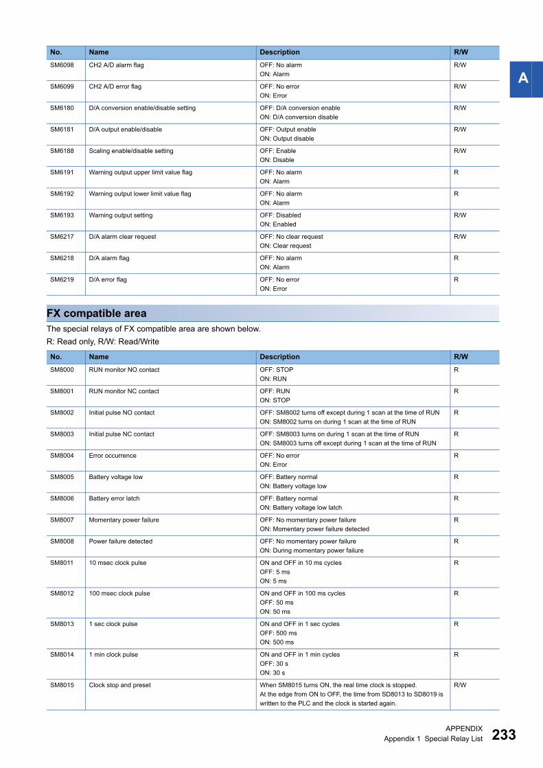
APPENDIX
Appendix 1 Special Relay List 233
A
FX compatible area
The special relays of FX compatible area are shown below.
R: Read only, R/W: Read/Write
SM6098 CH2 A/D alarm flag OFF: No alarm
ON: Alarm
R/W
SM6099 CH2 A/D error flag OFF: No error
ON: Error
R/W
SM6180 D/A conversion enable/disable setting OFF: D/A conversion enable
ON: D/A conversion disable
R/W
SM6181 D/A output enable/disable OFF: Output enable
ON: Output disable
R/W
SM6188 Scaling enable/disable setting OFF: Enable
ON: Disable
R/W
SM6191 Warning output upper limit value flag OFF: No alarm
ON: Alarm
R
SM6192 Warning output lower limit value flag OFF: No alarm
ON: Alarm
R
SM6193 Warning output setting OFF: Disabled
ON: Enabled
R/W
SM6217 D/A alarm clear request OFF: No clear request
ON: Clear request
R/W
SM6218 D/A alarm flag OFF: No alarm
ON: Alarm
R
SM6219 D/A error flag OFF: No error
ON: Error
R
No. Name Description R/W
SM8000 RUN monitor NO contact OFF: STOP
ON: RUN
R
SM8001 RUN monitor NC contact OFF: RUN
ON: STOP
R
SM8002 Initial pulse NO contact OFF: SM8002 turns off except during 1 scan at the time of RUN
ON: SM8002 turns on during 1 scan at the time of RUN
R
SM8003 Initial pulse NC contact OFF: SM8003 turns on during 1 scan at the time of RUN
ON: SM8003 turns off except during 1 scan at the time of RUN
R
SM8004 Error occurrence OFF: No error
ON: Error
R
SM8005 Battery voltage low OFF: Battery normal
ON: Battery voltage low
R
SM8006 Battery error latch OFF: Battery normal
ON: Battery voltage low latch
R
SM8007 Momentary power failure OFF: No momentary power failure
ON: Momentary power failure detected
R
SM8008 Power failure detected OFF: No momentary power failure
ON: During momentary power failure
R
SM8011 10 msec clock pulse ON and OFF in 10 ms cycles
OFF: 5 ms
ON: 5 ms
R
SM8012 100 msec clock pulse ON and OFF in 100 ms cycles
OFF: 50 ms
ON: 50 ms
R
SM8013 1 sec clock pulse ON and OFF in 1 sec cycles
OFF: 500 ms
ON: 500 ms
R
SM8014 1 min clock pulse ON and OFF in 1 min cycles
OFF: 30 s
ON: 30 s
R
SM8015 Clock stop and preset When SM8015 turns ON, the real time clock is stopped.
At the edge from ON to OFF, the time from SD8013 to SD8019 is
written to the PLC and the clock is started again.
R/W
No. Name Description R/W
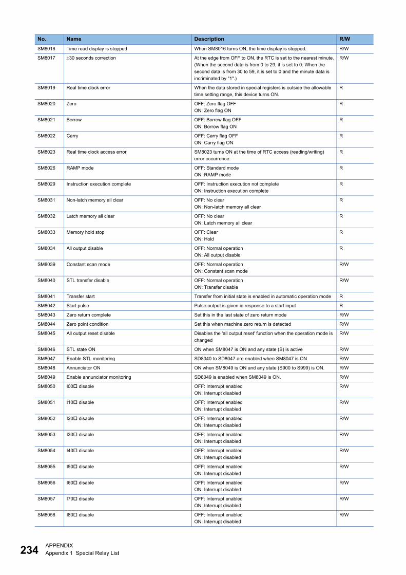
234APPENDIX
Appendix 1 Special Relay List
SM8016 Time read display is stopped When SM8016 turns ON, the time display is stopped. R/W
SM8017 30 seconds correction At the edge from OFF to ON, the RTC is set to the nearest minute.
(When the second data is from 0 to 29, it is set to 0. When the
second data is from 30 to 59, it is set to 0 and the minute data is
incriminated by "1".)
R/W
SM8019 Real time clock error When the data stored in special registers is outside the allowable
time setting range, this device turns ON.
R
SM8020 Zero OFF: Zero flag OFF
ON: Zero flag ON
R
SM8021 Borrow OFF: Borrow flag OFF
ON: Borrow flag ON
R
SM8022 Carry OFF: Carry flag OFF
ON: Carry flag ON
R
SM8023 Real time clock access error SM8023 turns ON at the time of RTC access (reading/writing)
error occurrence.
R
SM8026 RAMP mode OFF: Standard mode
ON: RAMP mode
R
SM8029 Instruction execution complete OFF: Instruction execution not complete
ON: Instruction execution complete
R
SM8031 Non-latch memory all clear OFF: No clear
ON: Non-latch memory all clear
R
SM8032 Latch memory all clear OFF: No clear
ON: Latch memory all clear
R
SM8033 Memory hold stop OFF: Clear
ON: Hold
R
SM8034 All output disable OFF: Normal operation
ON: All output disable
R
SM8039 Constant scan mode OFF: Normal operation
ON: Constant scan mode
R/W
SM8040 STL transfer disable OFF: Normal operation
ON: Transfer disable
R/W
SM8041 Transfer start Transfer from initial state is enabled in automatic operation mode R
SM8042 Start pulse Pulse output is given in response to a start input R
SM8043 Zero return complete Set this in the last state of zero return mode R/W
SM8044 Zero point condition Set this when machine zero return is detected R/W
SM8045 All output reset disable Disables the 'all output reset' function when the operation mode is
changed
R/W
SM8046 STL state ON ON when SM8047 is ON and any state (S) is active R/W
SM8047 Enable STL monitoring SD8040 to SD8047 are enabled when SM8047 is ON R/W
SM8048 Annunciator ON ON when SM8049 is ON and any state (S900 to S999) is ON. R/W
SM8049 Enable annunciator monitoring SD8049 is enabled when SM8049 is ON. R/W
SM8050 I00 disable OFF: Interrupt enabled
ON: Interrupt disabled
R/W
SM8051 I10 disable OFF: Interrupt enabled
ON: Interrupt disabled
R/W
SM8052 I20 disable OFF: Interrupt enabled
ON: Interrupt disabled
R/W
SM8053 I30 disable OFF: Interrupt enabled
ON: Interrupt disabled
R/W
SM8054 I40 disable OFF: Interrupt enabled
ON: Interrupt disabled
R/W
SM8055 I50 disable OFF: Interrupt enabled
ON: Interrupt disabled
R/W
SM8056 I60 disable OFF: Interrupt enabled
ON: Interrupt disabled
R/W
SM8057 I70 disable OFF: Interrupt enabled
ON: Interrupt disabled
R/W
SM8058 I80 disable OFF: Interrupt enabled
ON: Interrupt disabled
R/W
No. Name Description R/W
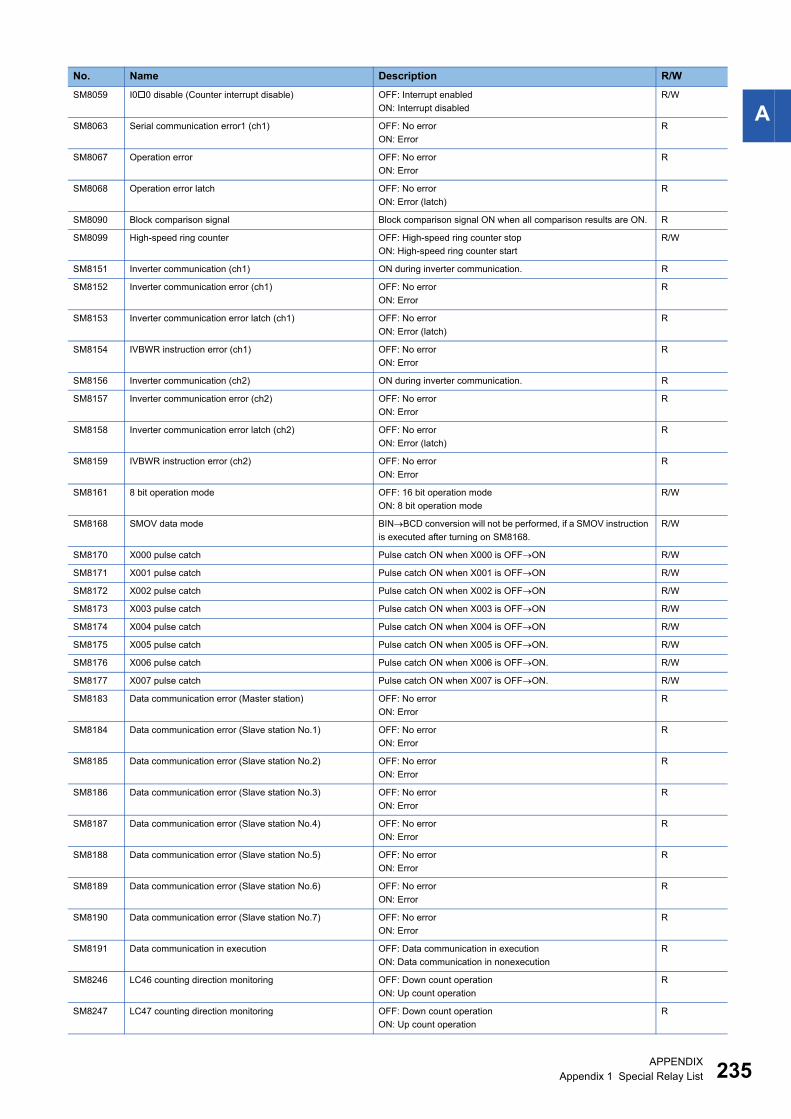
APPENDIX
Appendix 1 Special Relay List 235
ASM8059 I00 disable (Counter interrupt disable) OFF: Interrupt enabled
ON: Interrupt disabled
R/W
SM8063 Serial communication error1 (ch1) OFF: No error
ON: Error
R
SM8067 Operation error OFF: No error
ON: Error
R
SM8068 Operation error latch OFF: No error
ON: Error (latch)
R
SM8090 Block comparison signal Block comparison signal ON when all comparison results are ON. R
SM8099 High-speed ring counter OFF: High-speed ring counter stop
ON: High-speed ring counter start
R/W
SM8151 Inverter communication (ch1) ON during inverter communication. R
SM8152 Inverter communication error (ch1) OFF: No error
ON: Error
R
SM8153 Inverter communication error latch (ch1) OFF: No error
ON: Error (latch)
R
SM8154 IVBWR instruction error (ch1) OFF: No error
ON: Error
R
SM8156 Inverter communication (ch2) ON during inverter communication. R
SM8157 Inverter communication error (ch2) OFF: No error
ON: Error
R
SM8158 Inverter communication error latch (ch2) OFF: No error
ON: Error (latch)
R
SM8159 IVBWR instruction error (ch2) OFF: No error
ON: Error
R
SM8161 8 bit operation mode OFF: 16 bit operation mode
ON: 8 bit operation mode
R/W
SM8168 SMOV data mode BINBCD conversion will not be performed, if a SMOV instruction
is executed after turning on SM8168.
R/W
SM8170 X000 pulse catch Pulse catch ON when X000 is OFFON R/W
SM8171 X001 pulse catch Pulse catch ON when X001 is OFFON R/W
SM8172 X002 pulse catch Pulse catch ON when X002 is OFFON R/W
SM8173 X003 pulse catch Pulse catch ON when X003 is OFFON R/W
SM8174 X004 pulse catch Pulse catch ON when X004 is OFFON R/W
SM8175 X005 pulse catch Pulse catch ON when X005 is OFFON. R/W
SM8176 X006 pulse catch Pulse catch ON when X006 is OFFON. R/W
SM8177 X007 pulse catch Pulse catch ON when X007 is OFFON. R/W
SM8183 Data communication error (Master station) OFF: No error
ON: Error
R
SM8184 Data communication error (Slave station No.1) OFF: No error
ON: Error
R
SM8185 Data communication error (Slave station No.2) OFF: No error
ON: Error
R
SM8186 Data communication error (Slave station No.3) OFF: No error
ON: Error
R
SM8187 Data communication error (Slave station No.4) OFF: No error
ON: Error
R
SM8188 Data communication error (Slave station No.5) OFF: No error
ON: Error
R
SM8189 Data communication error (Slave station No.6) OFF: No error
ON: Error
R
SM8190 Data communication error (Slave station No.7) OFF: No error
ON: Error
R
SM8191 Data communication in execution OFF: Data communication in execution
ON: Data communication in nonexecution
R
SM8246 LC46 counting direction monitoring OFF: Down count operation
ON: Up count operation
R
SM8247 LC47 counting direction monitoring OFF: Down count operation
ON: Up count operation
R
No. Name Description R/W
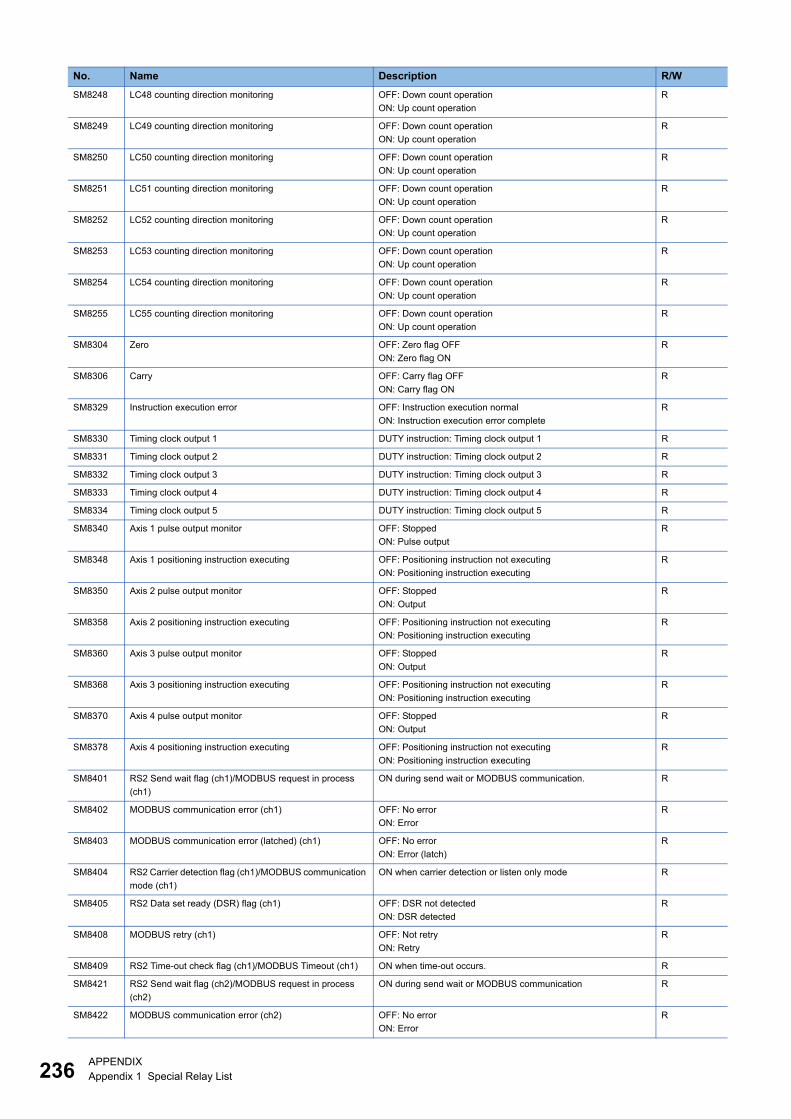
236APPENDIX
Appendix 1 Special Relay List
SM8248 LC48 counting direction monitoring OFF: Down count operation
ON: Up count operation
R
SM8249 LC49 counting direction monitoring OFF: Down count operation
ON: Up count operation
R
SM8250 LC50 counting direction monitoring OFF: Down count operation
ON: Up count operation
R
SM8251 LC51 counting direction monitoring OFF: Down count operation
ON: Up count operation
R
SM8252 LC52 counting direction monitoring OFF: Down count operation
ON: Up count operation
R
SM8253 LC53 counting direction monitoring OFF: Down count operation
ON: Up count operation
R
SM8254 LC54 counting direction monitoring OFF: Down count operation
ON: Up count operation
R
SM8255 LC55 counting direction monitoring OFF: Down count operation
ON: Up count operation
R
SM8304 Zero OFF: Zero flag OFF
ON: Zero flag ON
R
SM8306 Carry OFF: Carry flag OFF
ON: Carry flag ON
R
SM8329 Instruction execution error OFF: Instruction execution normal
ON: Instruction execution error complete
R
SM8330 Timing clock output 1 DUTY instruction: Timing clock output 1 R
SM8331 Timing clock output 2 DUTY instruction: Timing clock output 2 R
SM8332 Timing clock output 3 DUTY instruction: Timing clock output 3 R
SM8333 Timing clock output 4 DUTY instruction: Timing clock output 4 R
SM8334 Timing clock output 5 DUTY instruction: Timing clock output 5 R
SM8340 Axis 1 pulse output monitor OFF: Stopped
ON: Pulse output
R
SM8348 Axis 1 positioning instruction executing OFF: Positioning instruction not executing
ON: Positioning instruction executing
R
SM8350 Axis 2 pulse output monitor OFF: Stopped
ON: Output
R
SM8358 Axis 2 positioning instruction executing OFF: Positioning instruction not executing
ON: Positioning instruction executing
R
SM8360 Axis 3 pulse output monitor OFF: Stopped
ON: Output
R
SM8368 Axis 3 positioning instruction executing OFF: Positioning instruction not executing
ON: Positioning instruction executing
R
SM8370 Axis 4 pulse output monitor OFF: Stopped
ON: Output
R
SM8378 Axis 4 positioning instruction executing OFF: Positioning instruction not executing
ON: Positioning instruction executing
R
SM8401 RS2 Send wait flag (ch1)/MODBUS request in process
(ch1)
ON during send wait or MODBUS communication. R
SM8402 MODBUS communication error (ch1) OFF: No error
ON: Error
R
SM8403 MODBUS communication error (latched) (ch1) OFF: No error
ON: Error (latch)
R
SM8404 RS2 Carrier detection flag (ch1)/MODBUS communication
mode (ch1)
ON when carrier detection or listen only mode R
SM8405 RS2 Data set ready (DSR) flag (ch1) OFF: DSR not detected
ON: DSR detected
R
SM8408 MODBUS retry (ch1) OFF: Not retry
ON: Retry
R
SM8409 RS2 Time-out check flag (ch1)/MODBUS Timeout (ch1) ON when time-out occurs. R
SM8421 RS2 Send wait flag (ch2)/MODBUS request in process
(ch2)
ON during send wait or MODBUS communication R
SM8422 MODBUS communication error (ch2) OFF: No error
ON: Error
R
No. Name Description R/W
APPENDIX
Appendix 1 Special Relay List 237
A
Serial communication
The special relays for serial communication are shown below.
R: Read only, R/W: Read/Write
SM8423 MODBUS communication error (latched) (ch2) OFF: No error
ON: Error (latch)
R
SM8424 RS2 Carrier detection flag (ch2)/MODBUS communication
mode (ch2)
Carrier detection flag or listen only mode ON when operating. R
SM8425 RS2 Data set ready (DSR) flag (ch2) OFF: DSR not detected
ON: DSR detected
R
SM8428 MODBUS retry (ch2) OFF: No retry
ON: Retry
R
SM8429 RS2 Time-out check flag (ch2)/MODBUS Timeout (ch2) ON when timeout occurs. R
SM8438 Serial communication error 2 (ch2) OFF: No error
ON: Error
R
SM8492 IP address storage area write request If OFF to ON, the IP address setting stored in SD8492 to SD8497
will be written in the IP address storage area.
R/W
SM8493 IP address storage area write completed � It turns on, if the write to the IP address storage area is
completed. Moreover, it turns on also at the time of the write-in
failure.
� Turns OFF when IP address storage area write request
(SM8492) turns from ON to OFF.
R
SM8494 IP address storage area write error � Turns ON when writing to IP address storage area is failed.
� Turns ON if there is a problem in contents of IP address storage
area, when PLC power supply is turned from OFF to ON.
� Turns OFF when IP address storage area write request
(SM8492) turns from ON to OFF.
R
SM8495 IP address storage area clear request Contents of IP address storage area are cleared when this device
turns from OFF to ON.
R/W
SM8496 IP address storage area clear completed � It turns on, if the clear to the IP address storage area is
completed. Moreover, it turns on also at the time of the clear-in
failure.
� Turns OFF when IP address storage area clear request
(SM8495) turns from ON to OFF.
R
SM8497 IP address storage area clear error � Turns ON when clear to IP address storage area is failed.
� Turns OFF when IP address storage area clear request
(SM8495) turns from ON to OFF.
R
SM8498 IP address change function enable flag Turns ON when IP address is changed by IP address change
function.
R
No. Name Description R/W
SM8500 Serial communication error (ch1) OFF: No error
ON: Error
R
SM8510 Serial communication error (ch2) OFF: No error
ON: Error
R
SM8520 Serial communication error (ch3) OFF: No error
ON: Error
R
SM8530 Serial communication error (ch4) OFF: No error
ON: Error
R
SM8560 Data transfer delayed (ch1) This device remains ON while the PLC is waiting to send. R
SM8561 Data transfer flag (ch1) When this device is set to ON, the PLC starts to send. R
SM8562 Receive completion flag (ch1) This device turns ON when receiving is completed. R
SM8563 Carrier detection flag (ch1) This device turns ON in synchronization with the CD (DCD) signal. R
SM8564 Data set ready flag (ch1) This device turns ON in synchronization with the DR (DSR) signal. R
SM8565 Time-out check flag (ch1) This device turns ON when data receiving is suspended and the
next set of receive data is not given within the time set by the time-
out time setting device.
R
SM8570 Data transfer delayed (ch2) This device remains ON while the PLC is waiting to send. R
SM8571 Data transfer flag (ch2) When this device is set to ON, the PLC starts to send. R
SM8572 Receive completion flag (ch2) This device turns ON when receiving is completed. R
No. Name Description R/W
238APPENDIX
Appendix 1 Special Relay List
SM8573 Carrier detection flag (ch2) This device turns ON in synchronization with the CD (DCD) signal. R
SM8574 Data set ready flag (ch2) This device turns ON in synchronization with the DR (DSR) signal. R
SM8575 Time-out check flag (ch2) This device turns ON when data receiving is suspended and the
next set of receive data is not given within the time set by the time-
out time setting device.
R
SM8580 Data transfer delayed (ch3) This device remains ON while the PLC is waiting to send. R
SM8581 Data transfer flag (ch3) When this device is set to ON, the PLC starts to send. R
SM8582 Receive completion flag (ch3) This device turns ON when receiving is completed. R
SM8583 Carrier detection flag (ch3) This device turns ON in synchronization with the CD (DCD) signal. R
SM8584 Data set ready flag (ch3) This device turns ON in synchronization with the DR (DSR) signal. R
SM8585 Time-out check flag (ch3) This device turns ON when data receiving is suspended and the
next set of receive data is not given within the time set by the time-
out time setting device.
R
SM8590 Data transfer delayed (ch4) This device remains ON while the PLC is waiting to send R
SM8591 Data transfer flag (ch4) When this device is set to ON, the PLC starts to send R
SM8592 Receive completion flag (ch4) This device turns ON when receiving is completed R
SM8593 Carrier detection flag (ch4) This device turns ON in synchronization with the CD (DCD) signal R
SM8594 Data set ready flag (ch4) This device turns ON in synchronization with the DR (DSR) signal R
SM8595 Time-out check flag (ch4) This device turns ON when data receiving is suspended and the
next set of receive data is not given within the time set by the time-
out time setting device
R
SM8740 Station No. setting SD latch enabled (ch1) OFF: Latch disabled
ON: Latch enabled
R
SM8750 Station No. setting SD latch enabled (ch2) OFF: Latch disabled
ON: Latch enabled
R
SM8760 Station No. setting SD latch enabled (ch3) OFF: Latch disabled
ON: Latch enabled
R
SM8770 Station No. setting SD latch enabled (ch4) OFF: Latch disabled
ON: Latch enabled
R
SM8800 MODBUS RTU communication (ch1) OFF: Communication stop
ON: Communication
R
SM8801 Retry (ch1) OFF: No retry
ON: Retry
R
SM8802 Timeout (ch1) OFF: No timeout
ON: Timeout
R
SM8810 MODBUS RTU communication (ch2) OFF: Communication stop
ON: Communication
R
SM8811 Retry (ch2) OFF: No retry
ON: Retry
R
SM8812 Timeout (ch2) OFF: Not timeout
ON: Timeout
R
SM8820 MODBUS RTU communication (ch3) OFF: Communication stop
ON: Communication
R
SM8821 Retry (ch3) OFF: No retry
ON: Retry
R
SM8822 Timeout (ch3) OFF: No timeout
ON: Timeout
R
SM8830 MODBUS RTU communication (ch4) OFF: Communication stop
ON: Communication
R
SM8831 Retry (ch4) OFF: No retry
ON: Retry
R
SM8832 Timeout (ch4) OFF: No timeout
ON: Timeout
R
SM8861 Host station No. setting SD latch enabled (ch1) OFF: Latch disabled
ON: Latch enabled
R
SM8871 Host station No. setting SD latch enabled (ch2) OFF: Latch disabled
ON: Latch enabled
R
SM8881 Host station No. setting SD latch enabled (ch3) OFF: Latch disabled
ON: Latch enabled
R
No. Name Description R/W
APPENDIX
Appendix 1 Special Relay List 239
ASM8891 Host station No. setting SD latch enabled (ch4) OFF: Latch disabled
ON: Latch enabled
R
SM8920 Inverter communication (ch1) OFF: No communication
ON: Communication
R
SM8921 IVBWR instruction error (ch1) OFF: No error
ON: Error
R
SM8930 Inverter communication (ch2) OFF: No communication
ON: Communication
R
SM8931 IVBWR instruction error (ch2) OFF: No error
ON: Error
R
SM8940 Inverter communication (ch3) OFF: No communication
ON: Communication
R
SM8941 IVBWR instruction error (ch3) OFF: No error
ON: Error
R
SM8950 Inverter communication (ch4) OFF: No communication
ON: Communication
R
SM8951 IVBWR instruction error (ch4) OFF: No error
ON: Error
R
SM9040 Data communication error (Master station) OFF: No error
ON: Error
R
SM9041 Data communication error (Slave station No.1) OFF: No error
ON: Error
R
SM9042 Data communication error (Slave station No.2) OFF: No error
ON: Error
R
SM9043 Data communication error (Slave station No.3) OFF: No error
ON: Error
R
SM9044 Data communication error (Slave station No.4) OFF: No error
ON: Error
R
SM9045 Data communication error (Slave station No.5) OFF: No error
ON: Error
R
SM9046 Data communication error (Slave station No.6) OFF: No error
ON: Error
R
SM9047 Data communication error (Slave station No.7) OFF: No error
ON: Error
R
SM9056 Data communication in execution OFF: Data communication in execution
ON: Data communication in nonexecution
R
SM9080 Station No. setting SD latch enabled OFF: Latch disabled
ON: Latch enabled
R
SM9081 Slave station total number setting SD latch enabled OFF: Latch disabled
ON: Latch enabled
R
No. Name Description R/W
240APPENDIX
Appendix 2 Special Register List
Appendix 2 Special Register List
Diagnostic information
The special register for diagnostic information are shown below.
R: Read only, R/W: Read/Write
No. Name Description R/W
SD0 Latest self diagnostics error code This register stores the latest self-diagnosis error code. R
SD1 Clock time for self diagnosis error occurrence (Year) This register stores the latest self-diagnosis error time (Year). R
SD2 Clock time for self diagnosis error occurrence (Month) This register stores the latest self-diagnosis error time (Month). R
SD3 Clock time for self diagnosis error occurrence (Day) This register stores the latest self-diagnosis error time (Day). R
SD4 Clock time for self diagnosis error occurrence (Hour) This register stores the latest self-diagnosis error time (Hour). R
SD5 Clock time for self diagnosis error occurrence (Minute) This register stores the latest self-diagnosis error time (Minute). R
SD6 Clock time for self diagnosis error occurrence (Second) This register stores the latest self-diagnosis error time (Second). R
SD7 Clock time for self diagnosis error occurrence (Day Week) This register stores the latest self-diagnosis error time (Day Week). R
SD10 Self diagnostics error code 1 This register stores the self-diagnosis error code. R
SD11 Self diagnostics error code 2 This register stores the self-diagnosis error code. R
SD12 Self diagnostics error code 3 This register stores the self-diagnosis error code. R
SD13 Self diagnostics error code 4 This register stores the self-diagnosis error code. R
SD14 Self diagnostics error code 5 This register stores the self-diagnosis error code. R
SD15 Self diagnostics error code 6 This register stores the self-diagnosis error code. R
SD16 Self diagnostics error code 7 This register stores the self-diagnosis error code. R
SD17 Self diagnostics error code 8 This register stores the self-diagnosis error code. R
SD18 Self diagnostics error code 9 This register stores the self-diagnosis error code. R
SD19 Self diagnostics error code 10 This register stores the self-diagnosis error code. R
SD20 Self diagnostics error code 11 This register stores the self-diagnosis error code. R
SD21 Self diagnostics error code 12 This register stores the self-diagnosis error code. R
SD22 Self diagnostics error code 13 This register stores the self-diagnosis error code. R
SD23 Self diagnostics error code 14 This register stores the self-diagnosis error code. R
SD24 Self diagnostics error code 15 This register stores the self-diagnosis error code. R
SD25 Self diagnostics error code 16 This register stores the self-diagnosis error code. R
SD53 The number of AC/DC DOWN detections This register stores the number of times of momentary power failure. R
SD61 I/O Module Verify Error Module No. This register stores the I/O module verify error module No.. R
SD62 Annunciator (F) Detection No. This register stores the earliest detected annunciator (F) No.. R
SD63 Annunciator (F) Detection Number This register stores the number of annunciator (F) detections. R
SD64 to
SD79
Annunciator (F) Detection No. table This register stores the annunciator (F) detection No. R
SD80 Detailed information 1 information category � Detailed information 1 information category code is stored.
� The following codes are stored into the information category code.
0: N/A
1: Program position information
2: Drive number and file name
4: Parameter information
5: System configuration information
6: Number of times information
7: Time information
R
Not used (fixed to 0) Information category code
b15 to b8 b7 to b0
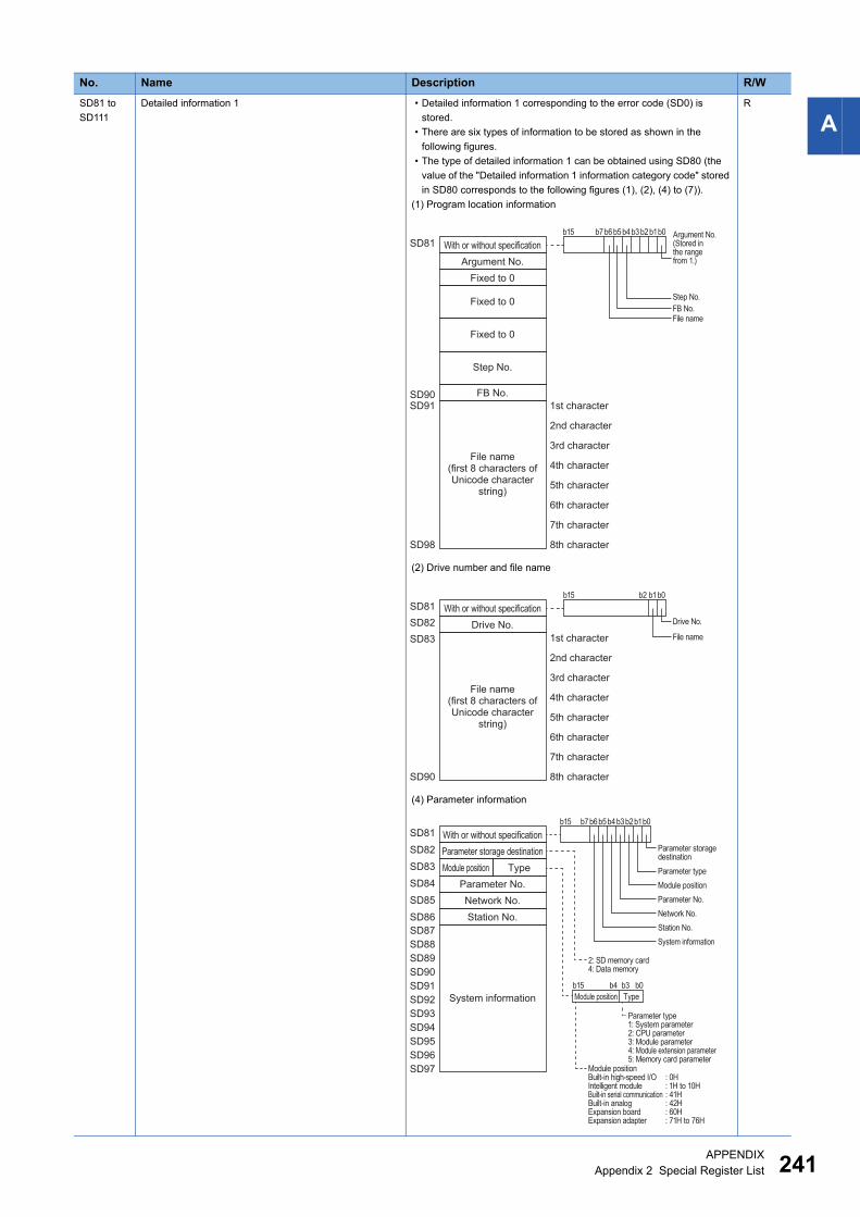
APPENDIX
Appendix 2 Special Register List 241
ASD81 to
SD111
Detailed information 1 � Detailed information 1 corresponding to the error code (SD0) is
stored.
� There are six types of information to be stored as shown in the
following figures.
� The type of detailed information 1 can be obtained using SD80 (the
value of the "Detailed information 1 information category code" stored
in SD80 corresponds to the following figures (1), (2), (4) to (7)).
(1) Program location information
(2) Drive number and file name
(4) Parameter information
R
No. Name Description R/W
With or without specification
b15 b1b0b2b3b4b5b6b7
SD81
SD98
SD91SD90
Argument No.
Fixed to 0
Fixed to 0
Fixed to 0
Step No.
1st character
2nd character
3rd character
4th character
5th character
6th character
7th character
8th character
FB No.
File name (first 8 characters of Unicode character
string)
Argument No.(Stored inthe rangefrom 1.)
Step No.
FB No.File name
With or without specification
b15 b1b0b2
SD81
SD82
SD83
SD90
Drive No.
1st character
2nd character
3rd character
4th character
5th character
6th character
7th character
8th character
File name(first 8 characters of Unicode character
string)
Drive No.
File name
With or without specification
b15 b1b0b2b3b4b5b6
b15 b0b3b4
b7
SD81
SD82
SD83
SD84
SD85
SD86
SD87
SD88
SD89
SD90
SD91
SD92
SD93
SD94
SD95
SD96
SD97
Module position Type
Parameter storage destination
Parameter No.
Network No.
Station No.
System information
Parameter storagedestination
Parameter type
Module position
Parameter No.
Network No.
Station No.
System information
Module position Type
2: SD memory card4: Data memory
Parameter type1: System parameter2: CPU parameter3: Module parameter4: Module extension parameter5: Memory card parameter
Module positionBuilt-in high-speed I/O : 0HIntelligent module : 1H to 10HBuilt-in serial communication : 41HBuilt-in analog : 42HExpansion board : 60HExpansion adapter : 71H to 76H
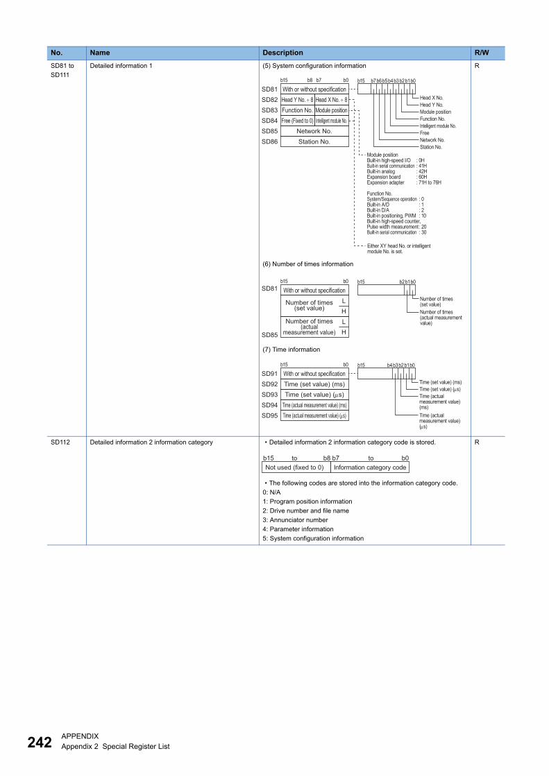
242APPENDIX
Appendix 2 Special Register List
SD81 to
SD111
Detailed information 1 (5) System configuration information
(6) Number of times information
(7) Time information
R
SD112 Detailed information 2 information category � Detailed information 2 information category code is stored.
� The following codes are stored into the information category code.
0: N/A
1: Program position information
2: Drive number and file name
3: Annunciator number
4: Parameter information
5: System configuration information
R
No. Name Description R/W
With or without specification
b15b15 b0b8 b7 b1b0b2b3b4b5b6b7
SD81
SD82
SD83
SD84
SD85
SD86
Function No. Module position
Head Y No. 8 Head X No. 8
Free (Fixed to 0) Intelligent module No.
Network No.
Station No.
Head X No.
Head Y No.
Module position
Function No.
Intelligent module No.
Free
Network No.
Station No.
Module positionBuilt-in high-speed I/O : 0HBuilt-in serial communication : 41HBuilt-in analog : 42HExpansion board : 60HExpansion adapter : 71H to 76H
Function No.System/Sequence operation : 0Built-in A/D : 1Built-in D/A : 2Built-in positioning, PWM : 10Built-in high-speed counter,Pulse width measurement : 20Built-in serial communication : 30
Either XY head No. or intelligent module No. is set.
With or without specification
b15b15 b1b0b0 b2
SD81
SD85
Number of times(set value)
L
H
L
H
Number of times(actual
measurement value)
Number of times (set value)
Number of times(actual measurement value)
With or without specification
b15 b1b0b2b3b4
SD91
SD92
SD93
SD94
SD95
Time (set value) (s)
Time (set value) (ms)
Time (actual measurement value) (ms)
Time (actual measurement value) (s)
Time (set value) (ms)
Time (set value) (s)
Time (actual measurement value) (ms)
Time (actual measurement value) (s)
b15 b0
Not used (fixed to 0) Information category code
b15 to b8 b7 to b0
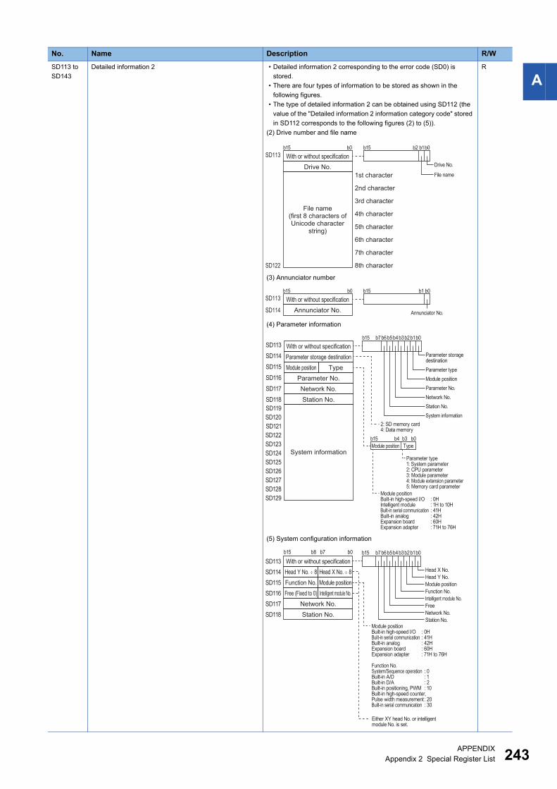
APPENDIX
Appendix 2 Special Register List 243
ASD113 to
SD143
Detailed information 2 � Detailed information 2 corresponding to the error code (SD0) is
stored.
� There are four types of information to be stored as shown in the
following figures.
� The type of detailed information 2 can be obtained using SD112 (the
value of the "Detailed information 2 information category code" stored
in SD112 corresponds to the following figures (2) to (5)).
(2) Drive number and file name
(3) Annunciator number
(4) Parameter information
(5) System configuration information
R
No. Name Description R/W
With or without specification
b15 b1b0b2
SD113
SD122
Drive No.
1st character
2nd character
3rd character
4th character
5th character
6th character
7th character
8th character
File name(first 8 characters of Unicode character
string)
Drive No.
File name
b15 b0
With or without specification
b15b15 b1 b0b0
SD113
SD114 Annunciator No. Annunciator No.
With or without specification
b15 b1b0b2b3b4b5b6
b15 b0b3b4
b7
SD113
SD114
SD115
SD116
SD117
SD118
SD119
SD120
SD121
SD122
SD123
SD124
SD125
SD126
SD127
SD128
SD129
Module position Type
Parameter storage destination
Parameter No.
Network No.
Station No.
System information
Parameter storagedestination
Parameter type
Module position
Parameter No.
Network No.
Station No.
System information
Module position Type
2: SD memory card4: Data memory
Parameter type1: System parameter2: CPU parameter3: Module parameter4: Module extension parameter5: Memory card parameter
Module positionBuilt-in high-speed I/O : 0HIntelligent module : 1H to 10HBuilt-in serial communication : 41HBuilt-in analog : 42HExpansion board : 60HExpansion adapter : 71H to 76H
With or without specification
b15 b0b8 b7
SD113
SD114
SD115
SD116
SD117
SD118
Function No. Module position
Head Y No. 8 Head X No. 8
Free (Fixed to 0) Intelligent module No.
Network No.
Station No.
Module positionBuilt-in high-speed I/O : 0HBuilt-in serial communication : 41HBuilt-in analog : 42HExpansion board : 60HExpansion adapter : 71H to 76H
Function No.System/Sequence operation : 0Built-in A/D : 1Built-in D/A : 2Built-in positioning, PWM : 10Built-in high-speed counter,Pulse width measurement : 20Built-in serial communication : 30
Either XY head No. or intelligent module No. is set.
b15 b1b0b2b3b4b5b6b7
Head X No.
Head Y No.
Module position
Function No.
Intelligent module No.
Free
Network No.
Station No.
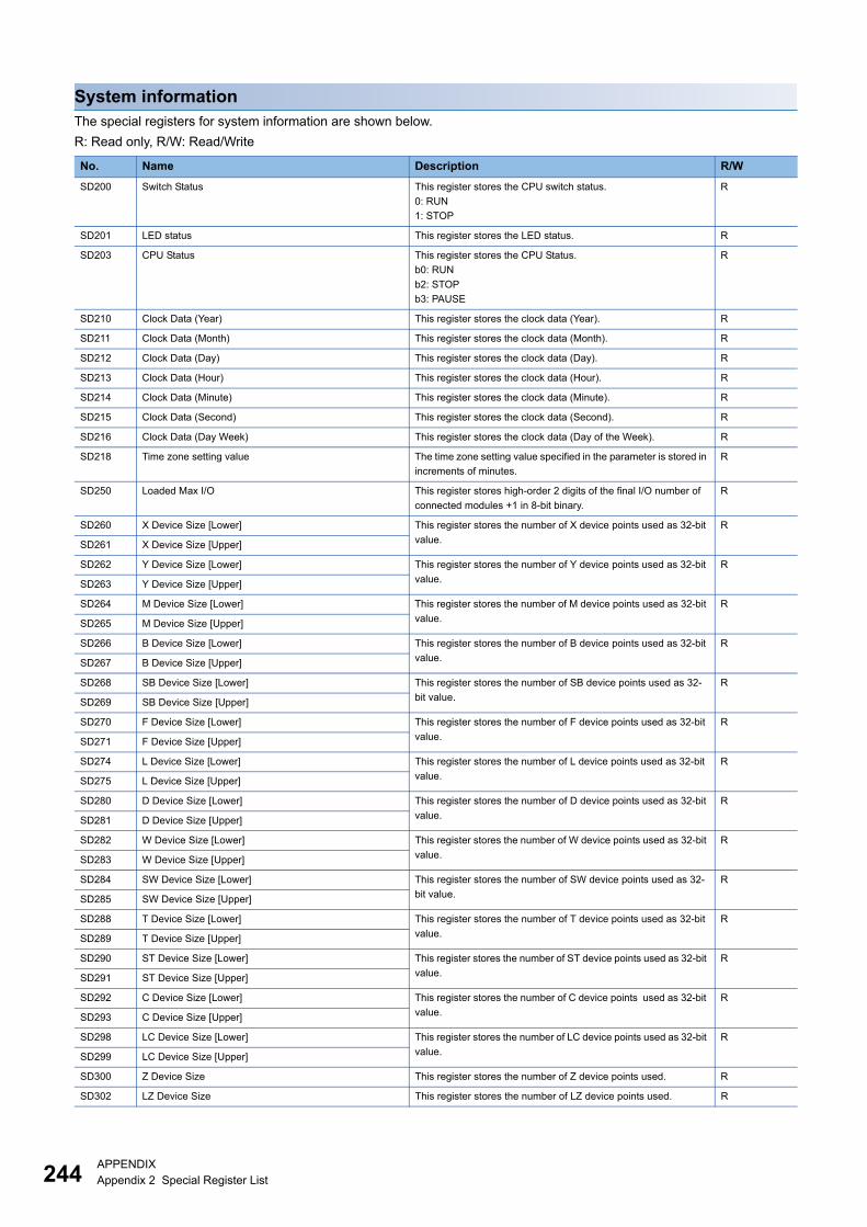
244APPENDIX
Appendix 2 Special Register List
System information
The special registers for system information are shown below.
R: Read only, R/W: Read/Write
No. Name Description R/W
SD200 Switch Status This register stores the CPU switch status.
0: RUN
1: STOP
R
SD201 LED status This register stores the LED status. R
SD203 CPU Status This register stores the CPU Status.
b0: RUN
b2: STOP
b3: PAUSE
R
SD210 Clock Data (Year) This register stores the clock data (Year). R
SD211 Clock Data (Month) This register stores the clock data (Month). R
SD212 Clock Data (Day) This register stores the clock data (Day). R
SD213 Clock Data (Hour) This register stores the clock data (Hour). R
SD214 Clock Data (Minute) This register stores the clock data (Minute). R
SD215 Clock Data (Second) This register stores the clock data (Second). R
SD216 Clock Data (Day Week) This register stores the clock data (Day of the Week). R
SD218 Time zone setting value The time zone setting value specified in the parameter is stored in
increments of minutes.
R
SD250 Loaded Max I/O This register stores high-order 2 digits of the final I/O number of
connected modules +1 in 8-bit binary.
R
SD260 X Device Size [Lower] This register stores the number of X device points used as 32-bit
value.
R
SD261 X Device Size [Upper]
SD262 Y Device Size [Lower] This register stores the number of Y device points used as 32-bit
value.
R
SD263 Y Device Size [Upper]
SD264 M Device Size [Lower] This register stores the number of M device points used as 32-bit
value.
R
SD265 M Device Size [Upper]
SD266 B Device Size [Lower] This register stores the number of B device points used as 32-bit
value.
R
SD267 B Device Size [Upper]
SD268 SB Device Size [Lower] This register stores the number of SB device points used as 32-
bit value.
R
SD269 SB Device Size [Upper]
SD270 F Device Size [Lower] This register stores the number of F device points used as 32-bit
value.
R
SD271 F Device Size [Upper]
SD274 L Device Size [Lower] This register stores the number of L device points used as 32-bit
value.
R
SD275 L Device Size [Upper]
SD280 D Device Size [Lower] This register stores the number of D device points used as 32-bit
value.
R
SD281 D Device Size [Upper]
SD282 W Device Size [Lower] This register stores the number of W device points used as 32-bit
value.
R
SD283 W Device Size [Upper]
SD284 SW Device Size [Lower] This register stores the number of SW device points used as 32-
bit value.
R
SD285 SW Device Size [Upper]
SD288 T Device Size [Lower] This register stores the number of T device points used as 32-bit
value.
R
SD289 T Device Size [Upper]
SD290 ST Device Size [Lower] This register stores the number of ST device points used as 32-bit
value.
R
SD291 ST Device Size [Upper]
SD292 C Device Size [Lower] This register stores the number of C device points used as 32-bit
value.
R
SD293 C Device Size [Upper]
SD298 LC Device Size [Lower] This register stores the number of LC device points used as 32-bit
value.
R
SD299 LC Device Size [Upper]
SD300 Z Device Size This register stores the number of Z device points used. R
SD302 LZ Device Size This register stores the number of LZ device points used. R
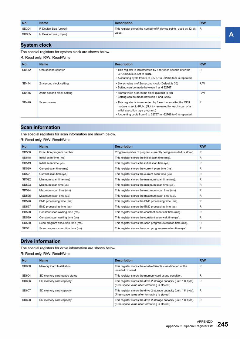
APPENDIX
Appendix 2 Special Register List 245
A
System clock
The special registers for system clock are shown below.
R: Read only, R/W: Read/Write
Scan information
The special registers for scan information are shown below.
R: Read only, R/W: Read/Write
Drive information
The special registers for drive information are shown below.
R: Read only, R/W: Read/Write
SD304 R Device Size [Lower] This register stores the number of R device points used as 32-bit
value.
R
SD305 R Device Size [Upper]
No. Name Description R/W
SD412 One second counter � This register is incremented by 1 for each second after the
CPU module is set to RUN.
� A counting cycle from 0 to 32767 to -32768 to 0 is repeated.
R
SD414 2n second clock setting � Stores value n of 2n second clock (Default is 30)
� Setting can be made between 1 and 32767.
R/W
SD415 2nms second clock setting � Stores value n of 2n ms clock (Default is 30)
� Setting can be made between 1 and 32767.
R/W
SD420 Scan counter � This register is incremented by 1 each scan after the CPU
module is set to RUN. (Not incremented for each scan of an
initial execution type program.)
� A counting cycle from 0 to 32767 to -32768 to 0 is repeated.
R
No. Name Description R/W
SD500 Execution program number Program number of program currently being executed is stored. R
SD518 Initial scan time (ms) This register stores the initial scan time (ms). R
SD519 Initial scan time (s) This register stores the initial scan time (s). R
SD520 Current scan time (ms) This register stores the current scan time (ms). R
SD521 Current scan time (s) This register stores the current scan time (s). R
SD522 Minimum scan time (ms) This register stores the minimum scan time (ms). R
SD523 Minimum scan time(s) This register stores the minimum scan time (s). R
SD524 Maximum scan time (ms) This register stores the maximum scan time (ms). R
SD525 Maximum scan time (s) This register stores the maximum scan time (s). R
SD526 END processing time (ms) This register stores the END processing time (ms). R
SD527 END processing time (s) This register stores the END processing time (s). R
SD528 Constant scan waiting time (ms) This register stores the constant scan wait time (ms). R
SD529 Constant scan waiting time (s) This register stores the constant scan wait time (s). R
SD530 Scan program execution time (ms) This register stores the scan program execution time (ms). R
SD531 Scan program execution time (s) This register stores the scan program execution time (s). R
No. Name Description R/W
SD600 Memory Card Installation This register stores the enable/disable classification of the
inserted SD card.
R
SD604 SD memory card usage status This register stores the memory card usage condition. R
SD606 SD memory card capacity This register stores the drive 2 storage capacity (unit: 1 K byte).
(Free space value after formatting is stored.)
R
SD607 SD memory card capacity This register stores the drive 2 storage capacity (unit: 1 K byte).
(Free space value after formatting is stored.)
R
SD608 SD memory card capacity This register stores the drive 2 storage capacity (unit: 1 K byte).
(Free space value after formatting is stored.)
R
No. Name Description R/W
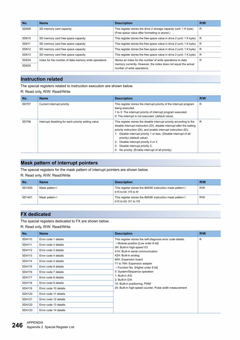
246APPENDIX
Appendix 2 Special Register List
Instruction related
The special registers related to instruction execution are shown below.
R: Read only, R/W: Read/Write
Mask pattern of interrupt pointers
The special registers for the mask pattern of interrupt pointers are shown below.
R: Read only, R/W: Read/Write
FX dedicated
The special registers dedicated to FX are shown below.
R: Read only, R/W: Read/Write
SD609 SD memory card capacity This register stores the drive 2 storage capacity (unit: 1 K byte).
(Free space value after formatting is stored.)
R
SD610 SD memory card free space capacity This register stores the free space value in drive 2 (unit: 1 K byte). R
SD611 SD memory card free space capacity This register stores the free space value in drive 2 (unit: 1 K byte). R
SD612 SD memory card free space capacity This register stores the free space value in drive 2 (unit: 1 K byte). R
SD613 SD memory card free space capacity This register stores the free space value in drive 2 (unit: 1 K byte). R
SD634 Index for the number of data memory write operations Stores an index for the number of write operations to data
memory currently. However, the index does not equal the actual
number of write operations.
R
SD635
No. Name Description R/W
SD757 Current interrupt priority This register stores the interrupt priority of the interrupt program
being executed.
1 to 3: The interrupt priority of interrupt program executed.
0: The interrupt is not executed. (default value)
R
SD758 Interrupt disabling for each priority setting value This register stores the disable interrupt priority according to the
disable interrupt instruction (DI), disable interrupt after the setting
priority instruction (DI), and enable interrupt instruction (EI).
1: Disable interrupt priority 1 or less. (Disable interrupt of all
priority) (default value)
2: Disable interrupt priority 2 or 3.
3: Disable interrupt priority 3.
0: No priority. (Enable interrupt of all priority)
R
No. Name Description R/W
SD1400 Mask pattern I This register stores the IMASK instruction mask pattern I.
b15 to b0: I15 to I0
R/W
SD1401 Mask pattern I This register stores the IMASK instruction mask pattern I.
b15 to b0: I31 to I16
R/W
No. Name Description R/W
SD4110 Error code 1 details This register stores the self-diagnosis error code details.
� Module position [Low order 8 bit]
0H: Built-in high-speed I/O
41H: Built-in serial communication
42H: Built-in analog
60H: Expansion board
71 to 76H: Expansion adapter
� Function No. [Higher order 8 bit]
0: System/Sequence operation
1: Built-in A/D
2: Built-in D/A
10: Built-in positioning, PWM
20: Built-in high-speed counter, Pulse width measurement
R
SD4111 Error code 2 details
SD4112 Error code 3 details
SD4113 Error code 4 details
SD4114 Error code 5 details
SD4115 Error code 6 details
SD4116 Error code 7 details
SD4117 Error code 8 details
SD4118 Error code 9 details
SD4119 Error code 10 details
SD4120 Error code 11 details
SD4121 Error code 12 details
SD4122 Error code 13 details
SD4123 Error code 14 details
No. Name Description R/W
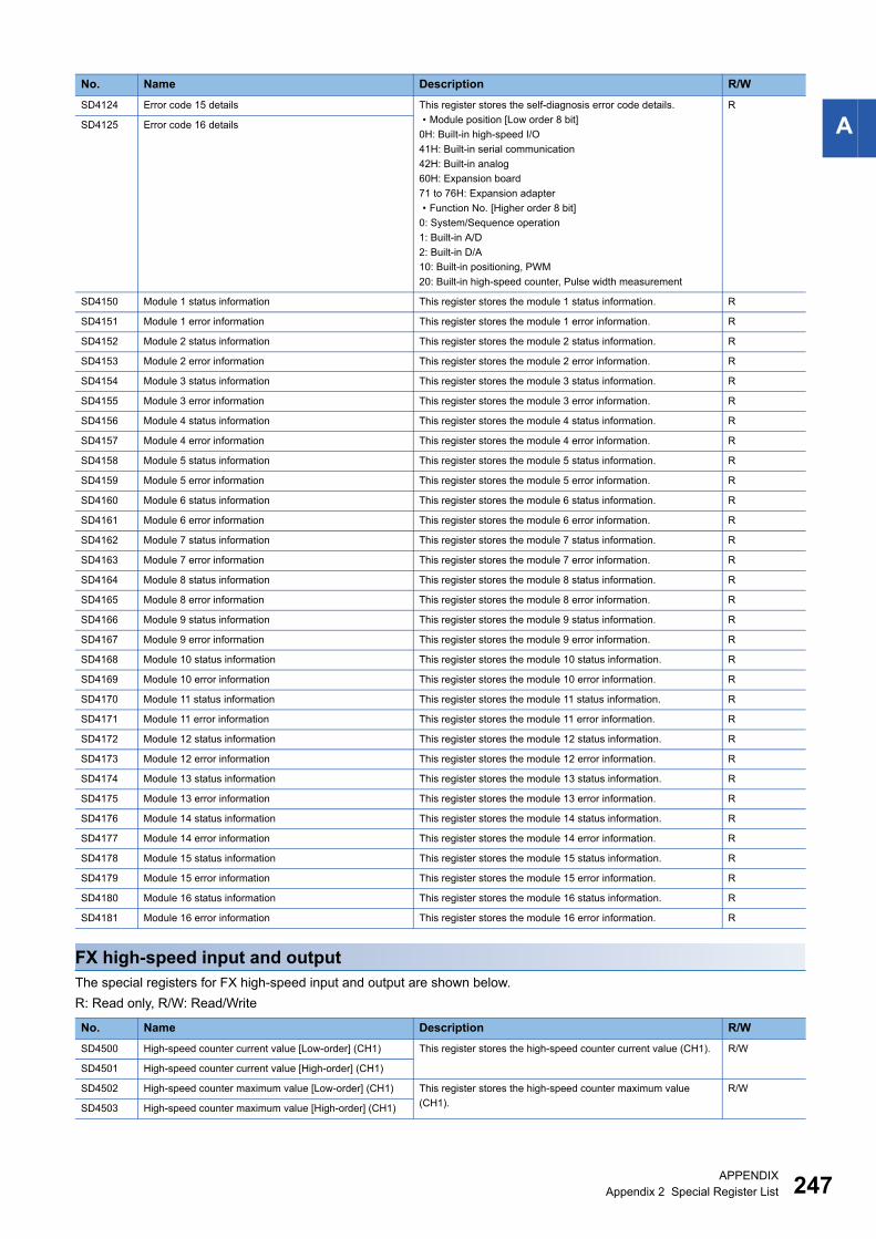
APPENDIX
Appendix 2 Special Register List 247
A
FX high-speed input and output
The special registers for FX high-speed input and output are shown below.
R: Read only, R/W: Read/Write
SD4124 Error code 15 details This register stores the self-diagnosis error code details.
� Module position [Low order 8 bit]
0H: Built-in high-speed I/O
41H: Built-in serial communication
42H: Built-in analog
60H: Expansion board
71 to 76H: Expansion adapter
� Function No. [Higher order 8 bit]
0: System/Sequence operation
1: Built-in A/D
2: Built-in D/A
10: Built-in positioning, PWM
20: Built-in high-speed counter, Pulse width measurement
R
SD4125 Error code 16 details
SD4150 Module 1 status information This register stores the module 1 status information. R
SD4151 Module 1 error information This register stores the module 1 error information. R
SD4152 Module 2 status information This register stores the module 2 status information. R
SD4153 Module 2 error information This register stores the module 2 error information. R
SD4154 Module 3 status information This register stores the module 3 status information. R
SD4155 Module 3 error information This register stores the module 3 error information. R
SD4156 Module 4 status information This register stores the module 4 status information. R
SD4157 Module 4 error information This register stores the module 4 error information. R
SD4158 Module 5 status information This register stores the module 5 status information. R
SD4159 Module 5 error information This register stores the module 5 error information. R
SD4160 Module 6 status information This register stores the module 6 status information. R
SD4161 Module 6 error information This register stores the module 6 error information. R
SD4162 Module 7 status information This register stores the module 7 status information. R
SD4163 Module 7 error information This register stores the module 7 error information. R
SD4164 Module 8 status information This register stores the module 8 status information. R
SD4165 Module 8 error information This register stores the module 8 error information. R
SD4166 Module 9 status information This register stores the module 9 status information. R
SD4167 Module 9 error information This register stores the module 9 error information. R
SD4168 Module 10 status information This register stores the module 10 status information. R
SD4169 Module 10 error information This register stores the module 10 error information. R
SD4170 Module 11 status information This register stores the module 11 status information. R
SD4171 Module 11 error information This register stores the module 11 error information. R
SD4172 Module 12 status information This register stores the module 12 status information. R
SD4173 Module 12 error information This register stores the module 12 error information. R
SD4174 Module 13 status information This register stores the module 13 status information. R
SD4175 Module 13 error information This register stores the module 13 error information. R
SD4176 Module 14 status information This register stores the module 14 status information. R
SD4177 Module 14 error information This register stores the module 14 error information. R
SD4178 Module 15 status information This register stores the module 15 status information. R
SD4179 Module 15 error information This register stores the module 15 error information. R
SD4180 Module 16 status information This register stores the module 16 status information. R
SD4181 Module 16 error information This register stores the module 16 error information. R
No. Name Description R/W
SD4500 High-speed counter current value [Low-order] (CH1) This register stores the high-speed counter current value (CH1). R/W
SD4501 High-speed counter current value [High-order] (CH1)
SD4502 High-speed counter maximum value [Low-order] (CH1) This register stores the high-speed counter maximum value
(CH1).
R/W
SD4503 High-speed counter maximum value [High-order] (CH1)
No. Name Description R/W
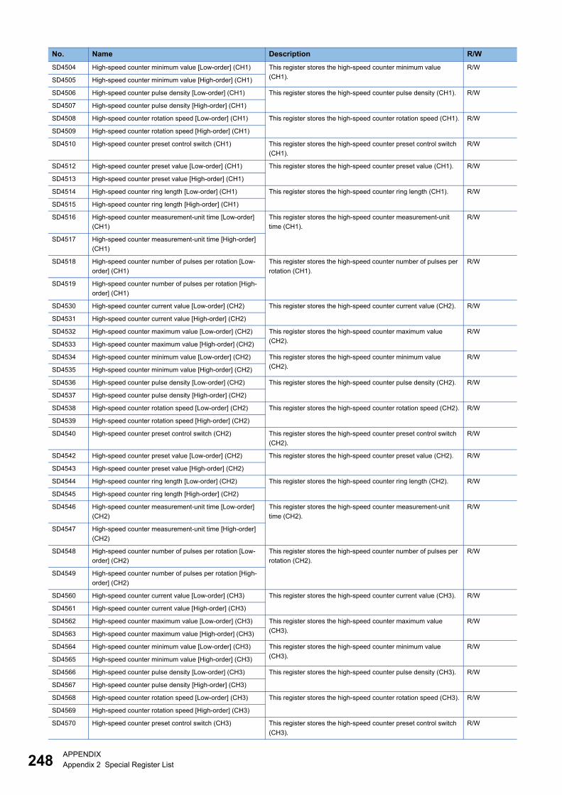
248APPENDIX
Appendix 2 Special Register List
SD4504 High-speed counter minimum value [Low-order] (CH1) This register stores the high-speed counter minimum value
(CH1).
R/W
SD4505 High-speed counter minimum value [High-order] (CH1)
SD4506 High-speed counter pulse density [Low-order] (CH1) This register stores the high-speed counter pulse density (CH1). R/W
SD4507 High-speed counter pulse density [High-order] (CH1)
SD4508 High-speed counter rotation speed [Low-order] (CH1) This register stores the high-speed counter rotation speed (CH1). R/W
SD4509 High-speed counter rotation speed [High-order] (CH1)
SD4510 High-speed counter preset control switch (CH1) This register stores the high-speed counter preset control switch
(CH1).
R/W
SD4512 High-speed counter preset value [Low-order] (CH1) This register stores the high-speed counter preset value (CH1). R/W
SD4513 High-speed counter preset value [High-order] (CH1)
SD4514 High-speed counter ring length [Low-order] (CH1) This register stores the high-speed counter ring length (CH1). R/W
SD4515 High-speed counter ring length [High-order] (CH1)
SD4516 High-speed counter measurement-unit time [Low-order]
(CH1)
This register stores the high-speed counter measurement-unit
time (CH1).
R/W
SD4517 High-speed counter measurement-unit time [High-order]
(CH1)
SD4518 High-speed counter number of pulses per rotation [Low-
order] (CH1)
This register stores the high-speed counter number of pulses per
rotation (CH1).
R/W
SD4519 High-speed counter number of pulses per rotation [High-
order] (CH1)
SD4530 High-speed counter current value [Low-order] (CH2) This register stores the high-speed counter current value (CH2). R/W
SD4531 High-speed counter current value [High-order] (CH2)
SD4532 High-speed counter maximum value [Low-order] (CH2) This register stores the high-speed counter maximum value
(CH2).
R/W
SD4533 High-speed counter maximum value [High-order] (CH2)
SD4534 High-speed counter minimum value [Low-order] (CH2) This register stores the high-speed counter minimum value
(CH2).
R/W
SD4535 High-speed counter minimum value [High-order] (CH2)
SD4536 High-speed counter pulse density [Low-order] (CH2) This register stores the high-speed counter pulse density (CH2). R/W
SD4537 High-speed counter pulse density [High-order] (CH2)
SD4538 High-speed counter rotation speed [Low-order] (CH2) This register stores the high-speed counter rotation speed (CH2). R/W
SD4539 High-speed counter rotation speed [High-order] (CH2)
SD4540 High-speed counter preset control switch (CH2) This register stores the high-speed counter preset control switch
(CH2).
R/W
SD4542 High-speed counter preset value [Low-order] (CH2) This register stores the high-speed counter preset value (CH2). R/W
SD4543 High-speed counter preset value [High-order] (CH2)
SD4544 High-speed counter ring length [Low-order] (CH2) This register stores the high-speed counter ring length (CH2). R/W
SD4545 High-speed counter ring length [High-order] (CH2)
SD4546 High-speed counter measurement-unit time [Low-order]
(CH2)
This register stores the high-speed counter measurement-unit
time (CH2).
R/W
SD4547 High-speed counter measurement-unit time [High-order]
(CH2)
SD4548 High-speed counter number of pulses per rotation [Low-
order] (CH2)
This register stores the high-speed counter number of pulses per
rotation (CH2).
R/W
SD4549 High-speed counter number of pulses per rotation [High-
order] (CH2)
SD4560 High-speed counter current value [Low-order] (CH3) This register stores the high-speed counter current value (CH3). R/W
SD4561 High-speed counter current value [High-order] (CH3)
SD4562 High-speed counter maximum value [Low-order] (CH3) This register stores the high-speed counter maximum value
(CH3).
R/W
SD4563 High-speed counter maximum value [High-order] (CH3)
SD4564 High-speed counter minimum value [Low-order] (CH3) This register stores the high-speed counter minimum value
(CH3).
R/W
SD4565 High-speed counter minimum value [High-order] (CH3)
SD4566 High-speed counter pulse density [Low-order] (CH3) This register stores the high-speed counter pulse density (CH3). R/W
SD4567 High-speed counter pulse density [High-order] (CH3)
SD4568 High-speed counter rotation speed [Low-order] (CH3) This register stores the high-speed counter rotation speed (CH3). R/W
SD4569 High-speed counter rotation speed [High-order] (CH3)
SD4570 High-speed counter preset control switch (CH3) This register stores the high-speed counter preset control switch
(CH3).
R/W
No. Name Description R/W
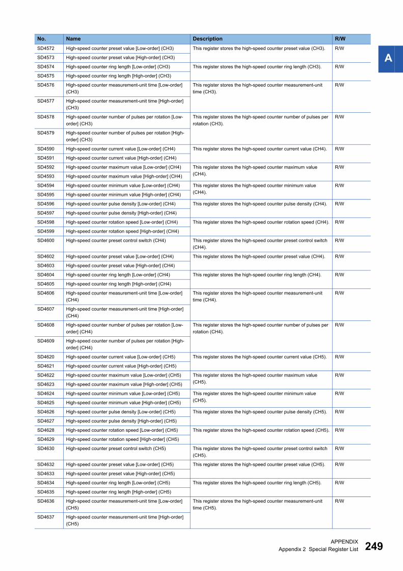
APPENDIX
Appendix 2 Special Register List 249
ASD4572 High-speed counter preset value [Low-order] (CH3) This register stores the high-speed counter preset value (CH3). R/W
SD4573 High-speed counter preset value [High-order] (CH3)
SD4574 High-speed counter ring length [Low-order] (CH3) This register stores the high-speed counter ring length (CH3). R/W
SD4575 High-speed counter ring length [High-order] (CH3)
SD4576 High-speed counter measurement-unit time [Low-order]
(CH3)
This register stores the high-speed counter measurement-unit
time (CH3).
R/W
SD4577 High-speed counter measurement-unit time [High-order]
(CH3)
SD4578 High-speed counter number of pulses per rotation [Low-
order] (CH3)
This register stores the high-speed counter number of pulses per
rotation (CH3).
R/W
SD4579 High-speed counter number of pulses per rotation [High-
order] (CH3)
SD4590 High-speed counter current value [Low-order] (CH4) This register stores the high-speed counter current value (CH4). R/W
SD4591 High-speed counter current value [High-order] (CH4)
SD4592 High-speed counter maximum value [Low-order] (CH4) This register stores the high-speed counter maximum value
(CH4).
R/W
SD4593 High-speed counter maximum value [High-order] (CH4)
SD4594 High-speed counter minimum value [Low-order] (CH4) This register stores the high-speed counter minimum value
(CH4).
R/W
SD4595 High-speed counter minimum value [High-order] (CH4)
SD4596 High-speed counter pulse density [Low-order] (CH4) This register stores the high-speed counter pulse density (CH4). R/W
SD4597 High-speed counter pulse density [High-order] (CH4)
SD4598 High-speed counter rotation speed [Low-order] (CH4) This register stores the high-speed counter rotation speed (CH4). R/W
SD4599 High-speed counter rotation speed [High-order] (CH4)
SD4600 High-speed counter preset control switch (CH4) This register stores the high-speed counter preset control switch
(CH4).
R/W
SD4602 High-speed counter preset value [Low-order] (CH4) This register stores the high-speed counter preset value (CH4). R/W
SD4603 High-speed counter preset value [High-order] (CH4)
SD4604 High-speed counter ring length [Low-order] (CH4) This register stores the high-speed counter ring length (CH4). R/W
SD4605 High-speed counter ring length [High-order] (CH4)
SD4606 High-speed counter measurement-unit time [Low-order]
(CH4)
This register stores the high-speed counter measurement-unit
time (CH4).
R/W
SD4607 High-speed counter measurement-unit time [High-order]
(CH4)
SD4608 High-speed counter number of pulses per rotation [Low-
order] (CH4)
This register stores the high-speed counter number of pulses per
rotation (CH4).
R/W
SD4609 High-speed counter number of pulses per rotation [High-
order] (CH4)
SD4620 High-speed counter current value [Low-order] (CH5) This register stores the high-speed counter current value (CH5). R/W
SD4621 High-speed counter current value [High-order] (CH5)
SD4622 High-speed counter maximum value [Low-order] (CH5) This register stores the high-speed counter maximum value
(CH5).
R/W
SD4623 High-speed counter maximum value [High-order] (CH5)
SD4624 High-speed counter minimum value [Low-order] (CH5) This register stores the high-speed counter minimum value
(CH5).
R/W
SD4625 High-speed counter minimum value [High-order] (CH5)
SD4626 High-speed counter pulse density [Low-order] (CH5) This register stores the high-speed counter pulse density (CH5). R/W
SD4627 High-speed counter pulse density [High-order] (CH5)
SD4628 High-speed counter rotation speed [Low-order] (CH5) This register stores the high-speed counter rotation speed (CH5). R/W
SD4629 High-speed counter rotation speed [High-order] (CH5)
SD4630 High-speed counter preset control switch (CH5) This register stores the high-speed counter preset control switch
(CH5).
R/W
SD4632 High-speed counter preset value [Low-order] (CH5) This register stores the high-speed counter preset value (CH5). R/W
SD4633 High-speed counter preset value [High-order] (CH5)
SD4634 High-speed counter ring length [Low-order] (CH5) This register stores the high-speed counter ring length (CH5). R/W
SD4635 High-speed counter ring length [High-order] (CH5)
SD4636 High-speed counter measurement-unit time [Low-order]
(CH5)
This register stores the high-speed counter measurement-unit
time (CH5).
R/W
SD4637 High-speed counter measurement-unit time [High-order]
(CH5)
No. Name Description R/W
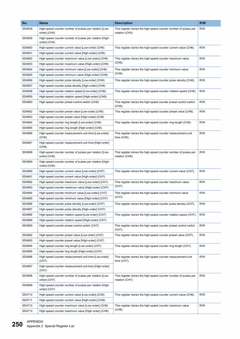
250APPENDIX
Appendix 2 Special Register List
SD4638 High-speed counter number of pulses per rotation [Low-
order] (CH5)
This register stores the high-speed counter number of pulses per
rotation (CH5).
R/W
SD4639 High-speed counter number of pulses per rotation [High-
order] (CH5)
SD4650 High-speed counter current value [Low-order] (CH6) This register stores the high-speed counter current value (CH6). R/W
SD4651 High-speed counter current value [High-order] (CH6)
SD4652 High-speed counter maximum value [Low-order] (CH6) This register stores the high-speed counter maximum value
(CH6).
R/W
SD4653 High-speed counter maximum value [High-order] (CH6)
SD4654 High-speed counter minimum value [Low-order] (CH6) This register stores the high-speed counter minimum value
(CH6).
R/W
SD4655 High-speed counter minimum value [High-order] (CH6)
SD4656 High-speed counter pulse density [Low-order] (CH6) This register stores the high-speed counter pulse density (CH6). R/W
SD4657 High-speed counter pulse density [High-order] (CH6)
SD4658 High-speed counter rotation speed [Low-order] (CH6) This register stores the high-speed counter rotation speed (CH6). R/W
SD4659 High-speed counter rotation speed [High-order] (CH6)
SD4660 High-speed counter preset control switch (CH6) This register stores the high-speed counter preset control switch
(CH6).
R/W
SD4662 High-speed counter preset value [Low-order] (CH6) This register stores the high-speed counter preset value (CH6). R/W
SD4663 High-speed counter preset value [High-order] (CH6)
SD4664 High-speed counter ring length [Low-order] (CH6) This register stores the high-speed counter ring length (CH6). R/W
SD4665 High-speed counter ring length [High-order] (CH6)
SD4666 High-speed counter measurement-unit time [Low-order]
(CH6)
This register stores the high-speed counter measurement-unit
time (CH6).
R/W
SD4667 High-speed counter measurement-unit time [High-order]
(CH6)
SD4668 High-speed counter number of pulses per rotation [Low-
order] (CH6)
This register stores the high-speed counter number of pulses per
rotation (CH6).
R/W
SD4669 High-speed counter number of pulses per rotation [High-
order] (CH6)
SD4680 High-speed counter current value [Low-order] (CH7) This register stores the high-speed counter current value (CH7). R/W
SD4681 High-speed counter current value [High-order] (CH7)
SD4682 High-speed counter maximum value [Low-order] (CH7) This register stores the high-speed counter maximum value
(CH7).
R/W
SD4683 High-speed counter maximum value [High-order] (CH7)
SD4684 High-speed counter minimum value [Low-order] (CH7) This register stores the high-speed counter minimum value
(CH7).
R/W
SD4685 High-speed counter minimum value [High-order] (CH7)
SD4686 High-speed counter pulse density [Low-order] (CH7) This register stores the high-speed counter pulse density (CH7). R/W
SD4687 High-speed counter pulse density [High-order] (CH7)
SD4688 High-speed counter rotation speed [Low-order] (CH7) This register stores the high-speed counter rotation speed (CH7). R/W
SD4689 High-speed counter rotation speed [High-order] (CH7)
SD4690 High-speed counter preset control switch (CH7) This register stores the high-speed counter preset control switch
(CH7).
R/W
SD4692 High-speed counter preset value [Low-order] (CH7) This register stores the high-speed counter preset value (CH7). R/W
SD4693 High-speed counter preset value [High-order] (CH7)
SD4694 High-speed counter ring length [Low-order] (CH7) This register stores the high-speed counter ring length (CH7). R/W
SD4695 High-speed counter ring length [High-order] (CH7)
SD4696 High-speed counter measurement-unit time [Low-order]
(CH7)
This register stores the high-speed counter measurement-unit
time (CH7).
R/W
SD4697 High-speed counter measurement-unit time [High-order]
(CH7)
SD4698 High-speed counter number of pulses per rotation [Low-
order] (CH7)
This register stores the high-speed counter number of pulses per
rotation (CH7).
R/W
SD4699 High-speed counter number of pulses per rotation [High-
order] (CH7)
SD4710 High-speed counter current value [Low-order] (CH8) This register stores the high-speed counter current value (CH8). R/W
SD4711 High-speed counter current value [High-order] (CH8)
SD4712 High-speed counter maximum value [Low-order] (CH8) This register stores the high-speed counter maximum value
(CH8).
R/W
SD4713 High-speed counter maximum value [High-order] (CH8)
No. Name Description R/W
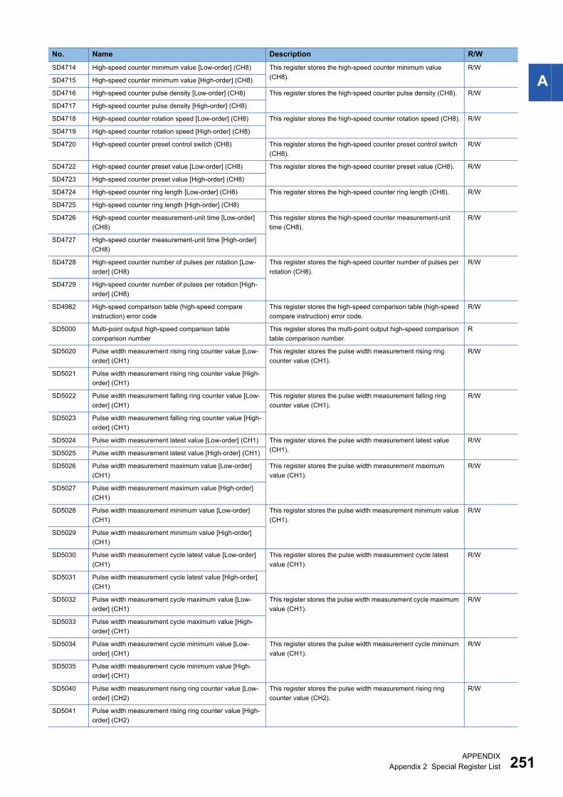
APPENDIX
Appendix 2 Special Register List 251
ASD4714 High-speed counter minimum value [Low-order] (CH8) This register stores the high-speed counter minimum value
(CH8).
R/W
SD4715 High-speed counter minimum value [High-order] (CH8)
SD4716 High-speed counter pulse density [Low-order] (CH8) This register stores the high-speed counter pulse density (CH8). R/W
SD4717 High-speed counter pulse density [High-order] (CH8)
SD4718 High-speed counter rotation speed [Low-order] (CH8) This register stores the high-speed counter rotation speed (CH8). R/W
SD4719 High-speed counter rotation speed [High-order] (CH8)
SD4720 High-speed counter preset control switch (CH8) This register stores the high-speed counter preset control switch
(CH8).
R/W
SD4722 High-speed counter preset value [Low-order] (CH8) This register stores the high-speed counter preset value (CH8). R/W
SD4723 High-speed counter preset value [High-order] (CH8)
SD4724 High-speed counter ring length [Low-order] (CH8) This register stores the high-speed counter ring length (CH8). R/W
SD4725 High-speed counter ring length [High-order] (CH8)
SD4726 High-speed counter measurement-unit time [Low-order]
(CH8)
This register stores the high-speed counter measurement-unit
time (CH8).
R/W
SD4727 High-speed counter measurement-unit time [High-order]
(CH8)
SD4728 High-speed counter number of pulses per rotation [Low-
order] (CH8)
This register stores the high-speed counter number of pulses per
rotation (CH8).
R/W
SD4729 High-speed counter number of pulses per rotation [High-
order] (CH8)
SD4982 High-speed comparison table (high-speed compare
instruction) error code
This register stores the high-speed comparison table (high-speed
compare instruction) error code.
R/W
SD5000 Multi-point output high-speed comparison table
comparison number
This register stores the multi-point output high-speed comparison
table comparison number.
R
SD5020 Pulse width measurement rising ring counter value [Low-
order] (CH1)
This register stores the pulse width measurement rising ring
counter value (CH1).
R/W
SD5021 Pulse width measurement rising ring counter value [High-
order] (CH1)
SD5022 Pulse width measurement falling ring counter value [Low-
order] (CH1)
This register stores the pulse width measurement falling ring
counter value (CH1).
R/W
SD5023 Pulse width measurement falling ring counter value [High-
order] (CH1)
SD5024 Pulse width measurement latest value [Low-order] (CH1) This register stores the pulse width measurement latest value
(CH1).
R/W
SD5025 Pulse width measurement latest value [High-order] (CH1)
SD5026 Pulse width measurement maximum value [Low-order]
(CH1)
This register stores the pulse width measurement maximum
value (CH1).
R/W
SD5027 Pulse width measurement maximum value [High-order]
(CH1)
SD5028 Pulse width measurement minimum value [Low-order]
(CH1)
This register stores the pulse width measurement minimum value
(CH1).
R/W
SD5029 Pulse width measurement minimum value [High-order]
(CH1)
SD5030 Pulse width measurement cycle latest value [Low-order]
(CH1)
This register stores the pulse width measurement cycle latest
value (CH1).
R/W
SD5031 Pulse width measurement cycle latest value [High-order]
(CH1)
SD5032 Pulse width measurement cycle maximum value [Low-
order] (CH1)
This register stores the pulse width measurement cycle maximum
value (CH1).
R/W
SD5033 Pulse width measurement cycle maximum value [High-
order] (CH1)
SD5034 Pulse width measurement cycle minimum value [Low-
order] (CH1)
This register stores the pulse width measurement cycle minimum
value (CH1).
R/W
SD5035 Pulse width measurement cycle minimum value [High-
order] (CH1)
SD5040 Pulse width measurement rising ring counter value [Low-
order] (CH2)
This register stores the pulse width measurement rising ring
counter value (CH2).
R/W
SD5041 Pulse width measurement rising ring counter value [High-
order] (CH2)
No. Name Description R/W
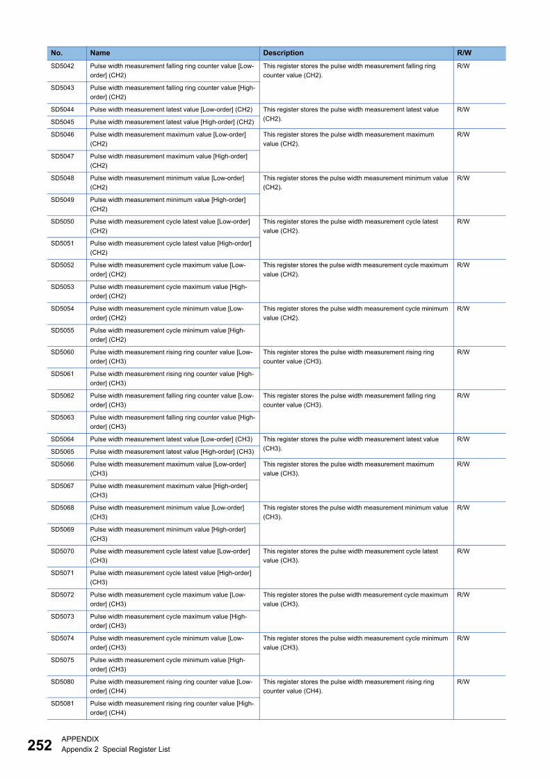
252APPENDIX
Appendix 2 Special Register List
SD5042 Pulse width measurement falling ring counter value [Low-
order] (CH2)
This register stores the pulse width measurement falling ring
counter value (CH2).
R/W
SD5043 Pulse width measurement falling ring counter value [High-
order] (CH2)
SD5044 Pulse width measurement latest value [Low-order] (CH2) This register stores the pulse width measurement latest value
(CH2).
R/W
SD5045 Pulse width measurement latest value [High-order] (CH2)
SD5046 Pulse width measurement maximum value [Low-order]
(CH2)
This register stores the pulse width measurement maximum
value (CH2).
R/W
SD5047 Pulse width measurement maximum value [High-order]
(CH2)
SD5048 Pulse width measurement minimum value [Low-order]
(CH2)
This register stores the pulse width measurement minimum value
(CH2).
R/W
SD5049 Pulse width measurement minimum value [High-order]
(CH2)
SD5050 Pulse width measurement cycle latest value [Low-order]
(CH2)
This register stores the pulse width measurement cycle latest
value (CH2).
R/W
SD5051 Pulse width measurement cycle latest value [High-order]
(CH2)
SD5052 Pulse width measurement cycle maximum value [Low-
order] (CH2)
This register stores the pulse width measurement cycle maximum
value (CH2).
R/W
SD5053 Pulse width measurement cycle maximum value [High-
order] (CH2)
SD5054 Pulse width measurement cycle minimum value [Low-
order] (CH2)
This register stores the pulse width measurement cycle minimum
value (CH2).
R/W
SD5055 Pulse width measurement cycle minimum value [High-
order] (CH2)
SD5060 Pulse width measurement rising ring counter value [Low-
order] (CH3)
This register stores the pulse width measurement rising ring
counter value (CH3).
R/W
SD5061 Pulse width measurement rising ring counter value [High-
order] (CH3)
SD5062 Pulse width measurement falling ring counter value [Low-
order] (CH3)
This register stores the pulse width measurement falling ring
counter value (CH3).
R/W
SD5063 Pulse width measurement falling ring counter value [High-
order] (CH3)
SD5064 Pulse width measurement latest value [Low-order] (CH3) This register stores the pulse width measurement latest value
(CH3).
R/W
SD5065 Pulse width measurement latest value [High-order] (CH3)
SD5066 Pulse width measurement maximum value [Low-order]
(CH3)
This register stores the pulse width measurement maximum
value (CH3).
R/W
SD5067 Pulse width measurement maximum value [High-order]
(CH3)
SD5068 Pulse width measurement minimum value [Low-order]
(CH3)
This register stores the pulse width measurement minimum value
(CH3).
R/W
SD5069 Pulse width measurement minimum value [High-order]
(CH3)
SD5070 Pulse width measurement cycle latest value [Low-order]
(CH3)
This register stores the pulse width measurement cycle latest
value (CH3).
R/W
SD5071 Pulse width measurement cycle latest value [High-order]
(CH3)
SD5072 Pulse width measurement cycle maximum value [Low-
order] (CH3)
This register stores the pulse width measurement cycle maximum
value (CH3).
R/W
SD5073 Pulse width measurement cycle maximum value [High-
order] (CH3)
SD5074 Pulse width measurement cycle minimum value [Low-
order] (CH3)
This register stores the pulse width measurement cycle minimum
value (CH3).
R/W
SD5075 Pulse width measurement cycle minimum value [High-
order] (CH3)
SD5080 Pulse width measurement rising ring counter value [Low-
order] (CH4)
This register stores the pulse width measurement rising ring
counter value (CH4).
R/W
SD5081 Pulse width measurement rising ring counter value [High-
order] (CH4)
No. Name Description R/W
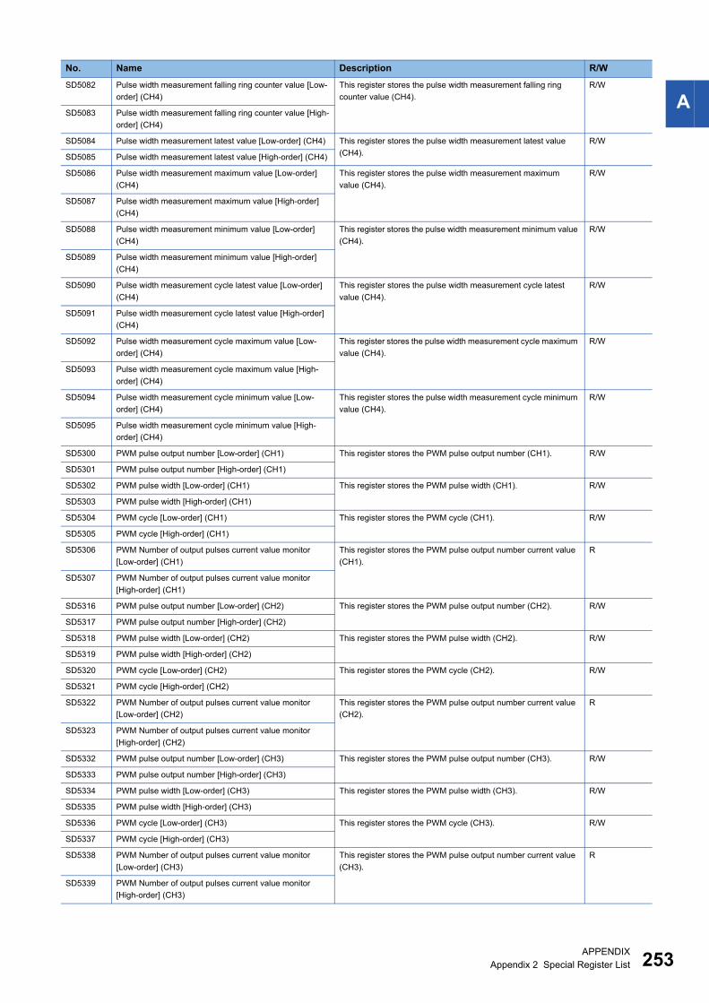
APPENDIX
Appendix 2 Special Register List 253
ASD5082 Pulse width measurement falling ring counter value [Low-
order] (CH4)
This register stores the pulse width measurement falling ring
counter value (CH4).
R/W
SD5083 Pulse width measurement falling ring counter value [High-
order] (CH4)
SD5084 Pulse width measurement latest value [Low-order] (CH4) This register stores the pulse width measurement latest value
(CH4).
R/W
SD5085 Pulse width measurement latest value [High-order] (CH4)
SD5086 Pulse width measurement maximum value [Low-order]
(CH4)
This register stores the pulse width measurement maximum
value (CH4).
R/W
SD5087 Pulse width measurement maximum value [High-order]
(CH4)
SD5088 Pulse width measurement minimum value [Low-order]
(CH4)
This register stores the pulse width measurement minimum value
(CH4).
R/W
SD5089 Pulse width measurement minimum value [High-order]
(CH4)
SD5090 Pulse width measurement cycle latest value [Low-order]
(CH4)
This register stores the pulse width measurement cycle latest
value (CH4).
R/W
SD5091 Pulse width measurement cycle latest value [High-order]
(CH4)
SD5092 Pulse width measurement cycle maximum value [Low-
order] (CH4)
This register stores the pulse width measurement cycle maximum
value (CH4).
R/W
SD5093 Pulse width measurement cycle maximum value [High-
order] (CH4)
SD5094 Pulse width measurement cycle minimum value [Low-
order] (CH4)
This register stores the pulse width measurement cycle minimum
value (CH4).
R/W
SD5095 Pulse width measurement cycle minimum value [High-
order] (CH4)
SD5300 PWM pulse output number [Low-order] (CH1) This register stores the PWM pulse output number (CH1). R/W
SD5301 PWM pulse output number [High-order] (CH1)
SD5302 PWM pulse width [Low-order] (CH1) This register stores the PWM pulse width (CH1). R/W
SD5303 PWM pulse width [High-order] (CH1)
SD5304 PWM cycle [Low-order] (CH1) This register stores the PWM cycle (CH1). R/W
SD5305 PWM cycle [High-order] (CH1)
SD5306 PWM Number of output pulses current value monitor
[Low-order] (CH1)
This register stores the PWM pulse output number current value
(CH1).
R
SD5307 PWM Number of output pulses current value monitor
[High-order] (CH1)
SD5316 PWM pulse output number [Low-order] (CH2) This register stores the PWM pulse output number (CH2). R/W
SD5317 PWM pulse output number [High-order] (CH2)
SD5318 PWM pulse width [Low-order] (CH2) This register stores the PWM pulse width (CH2). R/W
SD5319 PWM pulse width [High-order] (CH2)
SD5320 PWM cycle [Low-order] (CH2) This register stores the PWM cycle (CH2). R/W
SD5321 PWM cycle [High-order] (CH2)
SD5322 PWM Number of output pulses current value monitor
[Low-order] (CH2)
This register stores the PWM pulse output number current value
(CH2).
R
SD5323 PWM Number of output pulses current value monitor
[High-order] (CH2)
SD5332 PWM pulse output number [Low-order] (CH3) This register stores the PWM pulse output number (CH3). R/W
SD5333 PWM pulse output number [High-order] (CH3)
SD5334 PWM pulse width [Low-order] (CH3) This register stores the PWM pulse width (CH3). R/W
SD5335 PWM pulse width [High-order] (CH3)
SD5336 PWM cycle [Low-order] (CH3) This register stores the PWM cycle (CH3). R/W
SD5337 PWM cycle [High-order] (CH3)
SD5338 PWM Number of output pulses current value monitor
[Low-order] (CH3)
This register stores the PWM pulse output number current value
(CH3).
R
SD5339 PWM Number of output pulses current value monitor
[High-order] (CH3)
No. Name Description R/W
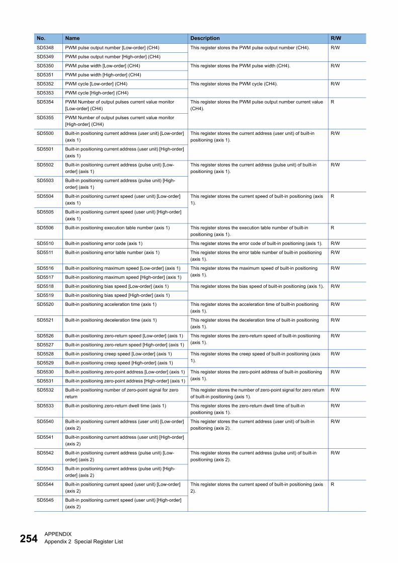
254APPENDIX
Appendix 2 Special Register List
SD5348 PWM pulse output number [Low-order] (CH4) This register stores the PWM pulse output number (CH4). R/W
SD5349 PWM pulse output number [High-order] (CH4)
SD5350 PWM pulse width [Low-order] (CH4) This register stores the PWM pulse width (CH4). R/W
SD5351 PWM pulse width [High-order] (CH4)
SD5352 PWM cycle [Low-order] (CH4) This register stores the PWM cycle (CH4). R/W
SD5353 PWM cycle [High-order] (CH4)
SD5354 PWM Number of output pulses current value monitor
[Low-order] (CH4)
This register stores the PWM pulse output number current value
(CH4).
R
SD5355 PWM Number of output pulses current value monitor
[High-order] (CH4)
SD5500 Built-in positioning current address (user unit) [Low-order]
(axis 1)
This register stores the current address (user unit) of built-in
positioning (axis 1).
R/W
SD5501 Built-in positioning current address (user unit) [High-order]
(axis 1)
SD5502 Built-in positioning current address (pulse unit) [Low-
order] (axis 1)
This register stores the current address (pulse unit) of built-in
positioning (axis 1).
R/W
SD5503 Built-in positioning current address (pulse unit) [High-
order] (axis 1)
SD5504 Built-in positioning current speed (user unit) [Low-order]
(axis 1)
This register stores the current speed of built-in positioning (axis
1).
R
SD5505 Built-in positioning current speed (user unit) [High-order]
(axis 1)
SD5506 Built-in positioning execution table number (axis 1) This register stores the execution table number of built-in
positioning (axis 1).
R
SD5510 Built-in positioning error code (axis 1) This register stores the error code of built-in positioning (axis 1). R/W
SD5511 Built-in positioning error table number (axis 1) This register stores the error table number of built-in positioning
(axis 1).
R/W
SD5516 Built-in positioning maximum speed [Low-order] (axis 1) This register stores the maximum speed of built-in positioning
(axis 1).
R/W
SD5517 Built-in positioning maximum speed [High-order] (axis 1)
SD5518 Built-in positioning bias speed [Low-order] (axis 1) This register stores the bias speed of built-in positioning (axis 1). R/W
SD5519 Built-in positioning bias speed [High-order] (axis 1)
SD5520 Built-in positioning acceleration time (axis 1) This register stores the acceleration time of built-in positioning
(axis 1).
R/W
SD5521 Built-in positioning deceleration time (axis 1) This register stores the deceleration time of built-in positioning
(axis 1).
R/W
SD5526 Built-in positioning zero-return speed [Low-order] (axis 1) This register stores the zero-return speed of built-in positioning
(axis 1).
R/W
SD5527 Built-in positioning zero-return speed [High-order] (axis 1)
SD5528 Built-in positioning creep speed [Low-order] (axis 1) This register stores the creep speed of built-in positioning (axis
1).
R/W
SD5529 Built-in positioning creep speed [High-order] (axis 1)
SD5530 Built-in positioning zero-point address [Low-order] (axis 1) This register stores the zero-point address of built-in positioning
(axis 1).
R/W
SD5531 Built-in positioning zero-point address [High-order] (axis 1)
SD5532 Built-in positioning number of zero-point signal for zero
return
This register stores the number of zero-point signal for zero return
of built-in positioning (axis 1).
R/W
SD5533 Built-in positioning zero-return dwell time (axis 1) This register stores the zero-return dwell time of built-in
positioning (axis 1).
R/W
SD5540 Built-in positioning current address (user unit) [Low-order]
(axis 2)
This register stores the current address (user unit) of built-in
positioning (axis 2).
R/W
SD5541 Built-in positioning current address (user unit) [High-order]
(axis 2)
SD5542 Built-in positioning current address (pulse unit) [Low-
order] (axis 2)
This register stores the current address (pulse unit) of built-in
positioning (axis 2).
R/W
SD5543 Built-in positioning current address (pulse unit) [High-
order] (axis 2)
SD5544 Built-in positioning current speed (user unit) [Low-order]
(axis 2)
This register stores the current speed of built-in positioning (axis
2).
R
SD5545 Built-in positioning current speed (user unit) [High-order]
(axis 2)
No. Name Description R/W
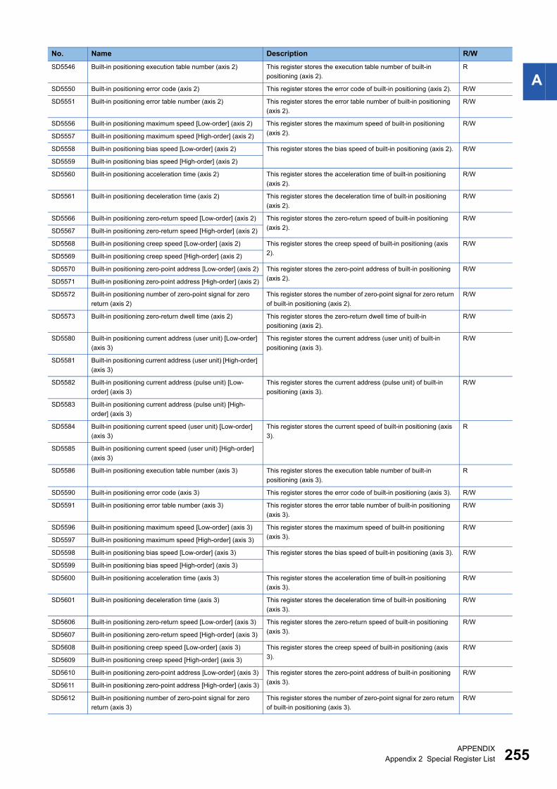
APPENDIX
Appendix 2 Special Register List 255
ASD5546 Built-in positioning execution table number (axis 2) This register stores the execution table number of built-in
positioning (axis 2).
R
SD5550 Built-in positioning error code (axis 2) This register stores the error code of built-in positioning (axis 2). R/W
SD5551 Built-in positioning error table number (axis 2) This register stores the error table number of built-in positioning
(axis 2).
R/W
SD5556 Built-in positioning maximum speed [Low-order] (axis 2) This register stores the maximum speed of built-in positioning
(axis 2).
R/W
SD5557 Built-in positioning maximum speed [High-order] (axis 2)
SD5558 Built-in positioning bias speed [Low-order] (axis 2) This register stores the bias speed of built-in positioning (axis 2). R/W
SD5559 Built-in positioning bias speed [High-order] (axis 2)
SD5560 Built-in positioning acceleration time (axis 2) This register stores the acceleration time of built-in positioning
(axis 2).
R/W
SD5561 Built-in positioning deceleration time (axis 2) This register stores the deceleration time of built-in positioning
(axis 2).
R/W
SD5566 Built-in positioning zero-return speed [Low-order] (axis 2) This register stores the zero-return speed of built-in positioning
(axis 2).
R/W
SD5567 Built-in positioning zero-return speed [High-order] (axis 2)
SD5568 Built-in positioning creep speed [Low-order] (axis 2) This register stores the creep speed of built-in positioning (axis
2).
R/W
SD5569 Built-in positioning creep speed [High-order] (axis 2)
SD5570 Built-in positioning zero-point address [Low-order] (axis 2) This register stores the zero-point address of built-in positioning
(axis 2).
R/W
SD5571 Built-in positioning zero-point address [High-order] (axis 2)
SD5572 Built-in positioning number of zero-point signal for zero
return (axis 2)
This register stores the number of zero-point signal for zero return
of built-in positioning (axis 2).
R/W
SD5573 Built-in positioning zero-return dwell time (axis 2) This register stores the zero-return dwell time of built-in
positioning (axis 2).
R/W
SD5580 Built-in positioning current address (user unit) [Low-order]
(axis 3)
This register stores the current address (user unit) of built-in
positioning (axis 3).
R/W
SD5581 Built-in positioning current address (user unit) [High-order]
(axis 3)
SD5582 Built-in positioning current address (pulse unit) [Low-
order] (axis 3)
This register stores the current address (pulse unit) of built-in
positioning (axis 3).
R/W
SD5583 Built-in positioning current address (pulse unit) [High-
order] (axis 3)
SD5584 Built-in positioning current speed (user unit) [Low-order]
(axis 3)
This register stores the current speed of built-in positioning (axis
3).
R
SD5585 Built-in positioning current speed (user unit) [High-order]
(axis 3)
SD5586 Built-in positioning execution table number (axis 3) This register stores the execution table number of built-in
positioning (axis 3).
R
SD5590 Built-in positioning error code (axis 3) This register stores the error code of built-in positioning (axis 3). R/W
SD5591 Built-in positioning error table number (axis 3) This register stores the error table number of built-in positioning
(axis 3).
R/W
SD5596 Built-in positioning maximum speed [Low-order] (axis 3) This register stores the maximum speed of built-in positioning
(axis 3).
R/W
SD5597 Built-in positioning maximum speed [High-order] (axis 3)
SD5598 Built-in positioning bias speed [Low-order] (axis 3) This register stores the bias speed of built-in positioning (axis 3). R/W
SD5599 Built-in positioning bias speed [High-order] (axis 3)
SD5600 Built-in positioning acceleration time (axis 3) This register stores the acceleration time of built-in positioning
(axis 3).
R/W
SD5601 Built-in positioning deceleration time (axis 3) This register stores the deceleration time of built-in positioning
(axis 3).
R/W
SD5606 Built-in positioning zero-return speed [Low-order] (axis 3) This register stores the zero-return speed of built-in positioning
(axis 3).
R/W
SD5607 Built-in positioning zero-return speed [High-order] (axis 3)
SD5608 Built-in positioning creep speed [Low-order] (axis 3) This register stores the creep speed of built-in positioning (axis
3).
R/W
SD5609 Built-in positioning creep speed [High-order] (axis 3)
SD5610 Built-in positioning zero-point address [Low-order] (axis 3) This register stores the zero-point address of built-in positioning
(axis 3).
R/W
SD5611 Built-in positioning zero-point address [High-order] (axis 3)
SD5612 Built-in positioning number of zero-point signal for zero
return (axis 3)
This register stores the number of zero-point signal for zero return
of built-in positioning (axis 3).
R/W
No. Name Description R/W
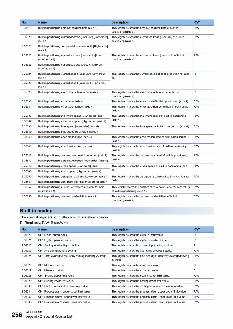
256APPENDIX
Appendix 2 Special Register List
Built-in analog
The special registers for built-in analog are shown below.
R: Read only, R/W: Read/Write
SD5613 Built-in positioning zero-return dwell time (axis 3) This register stores the zero-return dwell time of built-in
positioning (axis 3).
R/W
SD5620 Built-in positioning current address (user unit) [Low-order]
(axis 4)
This register stores the current address (user unit) of built-in
positioning (axis 4).
R/W
SD5621 Built-in positioning current address (user unit) [High-order]
(axis 4)
SD5622 Built-in positioning current address (pulse unit) [Low-
order] (axis 4)
This register stores the current address (pulse unit) of built-in
positioning (axis 4).
R/W
SD5623 Built-in positioning current address (pulse unit) [High-
order] (axis 4)
SD5624 Built-in positioning current speed (user unit) [Low-order]
(axis 4)
This register stores the current speed of built-in positioning (axis
4).
R
SD5625 Built-in positioning current speed (user unit) [High-order]
(axis 4)
SD5626 Built-in positioning execution table number (axis 4) This register stores the execution table number of built-in
positioning (axis 4).
R
SD5630 Built-in positioning error code (axis 4) This register stores the error code of built-in positioning (axis 4). R/W
SD5631 Built-in positioning error table number (axis 4) This register stores the error table number of built-in positioning
(axis 4).
R/W
SD5636 Built-in positioning maximum speed [Low-order] (axis 4) This register stores the maximum speed of built-in positioning
(axis 4).
R/W
SD5637 Built-in positioning maximum speed [High-order] (axis 4)
SD5638 Built-in positioning bias speed [Low-order] (axis 4) This register stores the bias speed of built-in positioning (axis 4). R/W
SD5639 Built-in positioning bias speed [High-order] (axis 4)
SD5640 Built-in positioning acceleration time (axis 4) This register stores the acceleration time of built-in positioning
(axis 4).
R/W
SD5641 Built-in positioning deceleration time (axis 4) This register stores the deceleration time of built-in positioning
(axis 4).
R/W
SD5646 Built-in positioning zero-return speed [Low-order] (axis 4) This register stores the zero-return speed of built-in positioning
(axis 4).
R/W
SD5647 Built-in positioning zero-return speed [High-order] (axis 4)
SD5648 Built-in positioning creep speed [Low-order] (axis 4) This register stores the creep speed of built-in positioning (axis
4).
R/W
SD5649 Built-in positioning creep speed [High-order] (axis 4)
SD5650 Built-in positioning zero-point address [Low-order] (axis 4) This register stores the zero-point address of built-in positioning
(axis 4).
R/W
SD5651 Built-in positioning zero-point address [High-order] (axis 4)
SD5652 Built-in positioning number of zero-point signal for zero
return (axis 4)
This register stores the number of zero-point signal for zero return
of built-in positioning (axis 4).
R/W
SD5653 Built-in positioning zero-return dwell time (axis 4) This register stores the zero-return dwell time of built-in
positioning (axis 4).
R/W
No. Name Description R/W
SD6020 CH1 Digital output value This register stores the digital output value. R
SD6021 CH1 Digital operation value This register stores the digital operation value. R
SD6022 CH1 Analog input voltage monitor This register stores the analog input voltage value. R
SD6023 CH1 Averaging process setting This register stores the averaging process setting. R/W
SD6024 CH1 Time Average/Frequency Average/Moving Average This register stores the time average/frequency average/moving
average.
R/W
SD6026 CH1 Maximum value This register stores the maximum value. R
SD6027 CH1 Minimum value This register stores the minimum value. R
SD6028 CH1 Scaling upper limit value This register stores the scaling upper limit value. R/W
SD6029 CH1 Scaling lower limit value This register stores the scaling lower limit value. R/W
SD6030 CH1 Shifting amount to conversion value This register stores the shifting amount of conversion value. R/W
SD6031 CH1 Process alarm upper upper limit value This register stores the process alarm upper upper limit value. R/W
SD6032 CH1 Process alarm upper lower limit value This register stores the process alarm upper lower limit value. R/W
SD6033 CH1 Process alarm lower upper limit value This register stores the process alarm lower upper limit value. R/W
No. Name Description R/W
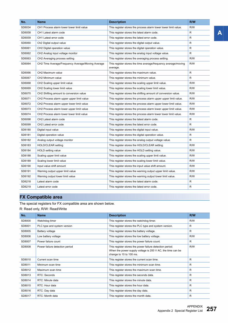
APPENDIX
Appendix 2 Special Register List 257
A
FX Compatible area
The special registers for FX compatible area are shown below.
R: Read only, R/W: Read/Write
SD6034 CH1 Process alarm lower lower limit value This register stores the process alarm lower lower limit value. R/W
SD6058 CH1 Latest alarm code This register stores the latest alarm code. R
SD6059 CH1 Latest error code This register stores the latest error code. R
SD6060 Ch2 Digital output value This register stores the digital output value. R
SD6061 CH2 Digital operation value This register stores the digital operation value. R
SD6062 CH2 Analog input voltage monitor This register stores the analog input voltage value. R
SD6063 CH2 Averaging process setting This register stores the averaging process setting. R/W
SD6064 CH2 Time Average/Frequency Average/Moving Average This register stores the time average/frequency average/moving
average.
R/W
SD6066 CH2 Maximum value This register stores the maximum value. R
SD6067 CH2 Minimum value This register stores the minimum value. R
SD6068 CH2 Scaling upper limit value This register stores the scaling upper limit value. R/W
SD6069 CH2 Scaling lower limit value This register stores the scaling lower limit value. R/W
SD6070 CH2 Shifting amount to conversion value This register stores the shifting amount of conversion value. R/W
SD6071 CH2 Process alarm upper upper limit value This register stores the process alarm upper upper limit value. R/W
SD6072 CH2 Process alarm upper lower limit value This register stores the process alarm upper lower limit value. R/W
SD6073 CH2 Process alarm lower upper limit value This register stores the process alarm lower upper limit value. R/W
SD6074 CH2 Process alarm lower lower limit value This register stores the process alarm lower lower limit value. R/W
SD6098 CH2 Latest alarm code This register stores the latest alarm code. R
SD6099 CH2 Latest error code This register stores the latest error code. R
SD6180 Digital input value This register stores the digital input value. R/W
SD6181 Digital operation value This register stores the digital operation value. R
SD6182 Analog output voltage monitor This register stores the analog output voltage value. R
SD6183 HOLD/CLEAR setting This register stores the HOLD/CLEAR setting. R/W
SD6184 HOLD setting value This register stores the HOLD setting value. R/W
SD6188 Scaling upper limit value This register stores the scaling upper limit value. R/W
SD6189 Scaling lower limit value This register stores the scaling lower limit value. R/W
SD6190 Input value shift amount This register stores the input value shift amount. R/W
SD6191 Warning output upper limit value This register stores the warning output upper limit value. R/W
SD6192 Warning output lower limit value This register stores the warning output lower limit value. R/W
SD6218 Latest alarm code This register stores the latest alarm code. R
SD6219 Latest error code This register stores the latest error code. R
No. Name Description R/W
SD8000 Watchdog timer This register stores the watchdog timer. R/W
SD8001 PLC type and system version This register stores the PLC type and system version. R
SD8005 Battery voltage This register stores the battery voltage. R
SD8006 Low battery voltage This register stores the low battery voltage. R/W
SD8007 Power failure count This register stores the power failure count. R
SD8008 Power failure detection period This register stores the power failure detection period.
When the power supply voltage is 200 V AC, the time can be
change to 10 to 100 ms.
R/W
SD8010 Current scan time This register stores the current scan time. R
SD8011 Minimum scan time This register stores the minimum scan time. R
SD8012 Maximum scan time This register stores the maximum scan time. R
SD8013 RTC: Seconds This register stores the seconds data. R
SD8014 RTC: Minute data This register stores the minute data. R
SD8015 RTC: Hour data This register stores the hour data. R
SD8016 RTC: Day data This register stores the day data. R
SD8017 RTC: Month data This register stores the month data. R
No. Name Description R/W
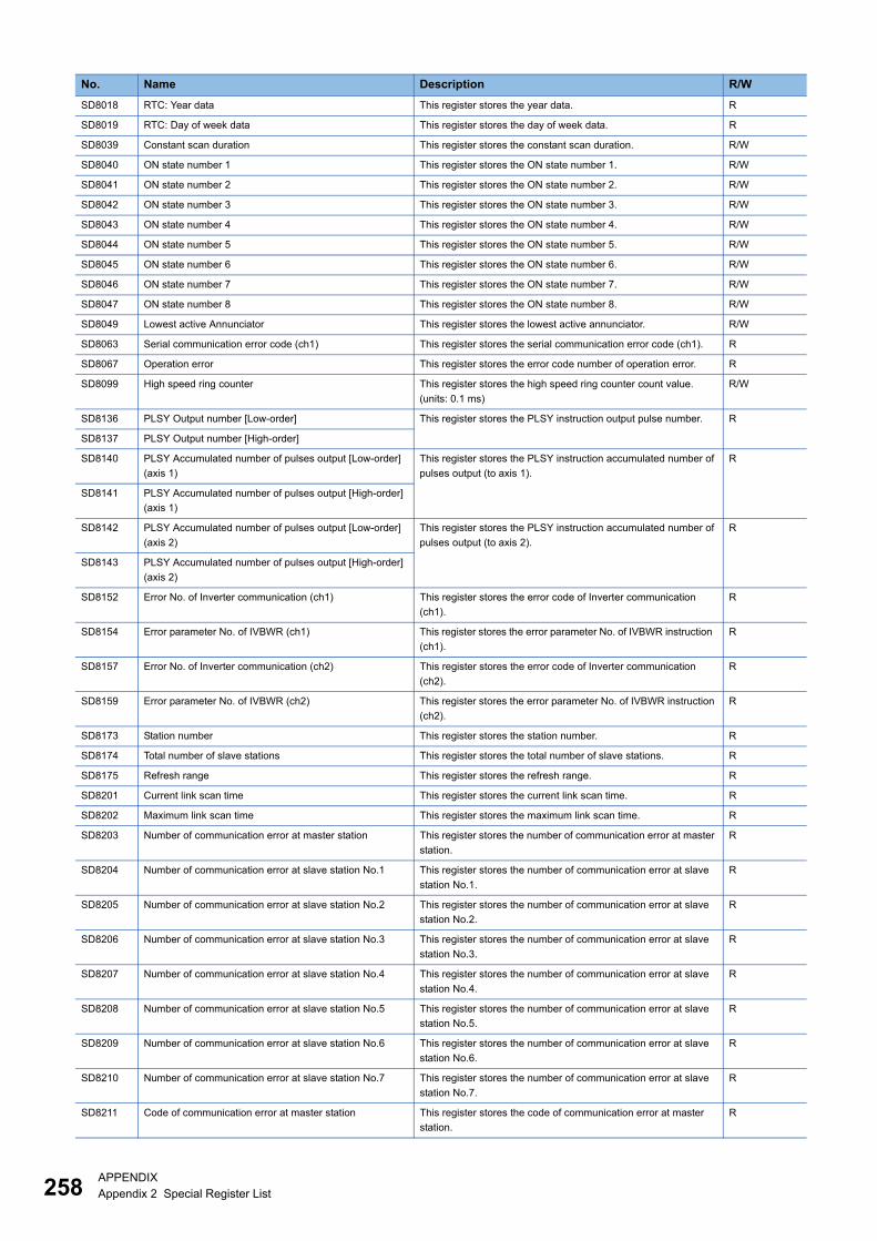
258APPENDIX
Appendix 2 Special Register List
SD8018 RTC: Year data This register stores the year data. R
SD8019 RTC: Day of week data This register stores the day of week data. R
SD8039 Constant scan duration This register stores the constant scan duration. R/W
SD8040 ON state number 1 This register stores the ON state number 1. R/W
SD8041 ON state number 2 This register stores the ON state number 2. R/W
SD8042 ON state number 3 This register stores the ON state number 3. R/W
SD8043 ON state number 4 This register stores the ON state number 4. R/W
SD8044 ON state number 5 This register stores the ON state number 5. R/W
SD8045 ON state number 6 This register stores the ON state number 6. R/W
SD8046 ON state number 7 This register stores the ON state number 7. R/W
SD8047 ON state number 8 This register stores the ON state number 8. R/W
SD8049 Lowest active Annunciator This register stores the lowest active annunciator. R/W
SD8063 Serial communication error code (ch1) This register stores the serial communication error code (ch1). R
SD8067 Operation error This register stores the error code number of operation error. R
SD8099 High speed ring counter This register stores the high speed ring counter count value.
(units: 0.1 ms)
R/W
SD8136 PLSY Output number [Low-order] This register stores the PLSY instruction output pulse number. R
SD8137 PLSY Output number [High-order]
SD8140 PLSY Accumulated number of pulses output [Low-order]
(axis 1)
This register stores the PLSY instruction accumulated number of
pulses output (to axis 1).
R
SD8141 PLSY Accumulated number of pulses output [High-order]
(axis 1)
SD8142 PLSY Accumulated number of pulses output [Low-order]
(axis 2)
This register stores the PLSY instruction accumulated number of
pulses output (to axis 2).
R
SD8143 PLSY Accumulated number of pulses output [High-order]
(axis 2)
SD8152 Error No. of Inverter communication (ch1) This register stores the error code of Inverter communication
(ch1).
R
SD8154 Error parameter No. of IVBWR (ch1) This register stores the error parameter No. of IVBWR instruction
(ch1).
R
SD8157 Error No. of Inverter communication (ch2) This register stores the error code of Inverter communication
(ch2).
R
SD8159 Error parameter No. of IVBWR (ch2) This register stores the error parameter No. of IVBWR instruction
(ch2).
R
SD8173 Station number This register stores the station number. R
SD8174 Total number of slave stations This register stores the total number of slave stations. R
SD8175 Refresh range This register stores the refresh range. R
SD8201 Current link scan time This register stores the current link scan time. R
SD8202 Maximum link scan time This register stores the maximum link scan time. R
SD8203 Number of communication error at master station This register stores the number of communication error at master
station.
R
SD8204 Number of communication error at slave station No.1 This register stores the number of communication error at slave
station No.1.
R
SD8205 Number of communication error at slave station No.2 This register stores the number of communication error at slave
station No.2.
R
SD8206 Number of communication error at slave station No.3 This register stores the number of communication error at slave
station No.3.
R
SD8207 Number of communication error at slave station No.4 This register stores the number of communication error at slave
station No.4.
R
SD8208 Number of communication error at slave station No.5 This register stores the number of communication error at slave
station No.5.
R
SD8209 Number of communication error at slave station No.6 This register stores the number of communication error at slave
station No.6.
R
SD8210 Number of communication error at slave station No.7 This register stores the number of communication error at slave
station No.7.
R
SD8211 Code of communication error at master station This register stores the code of communication error at master
station.
R
No. Name Description R/W
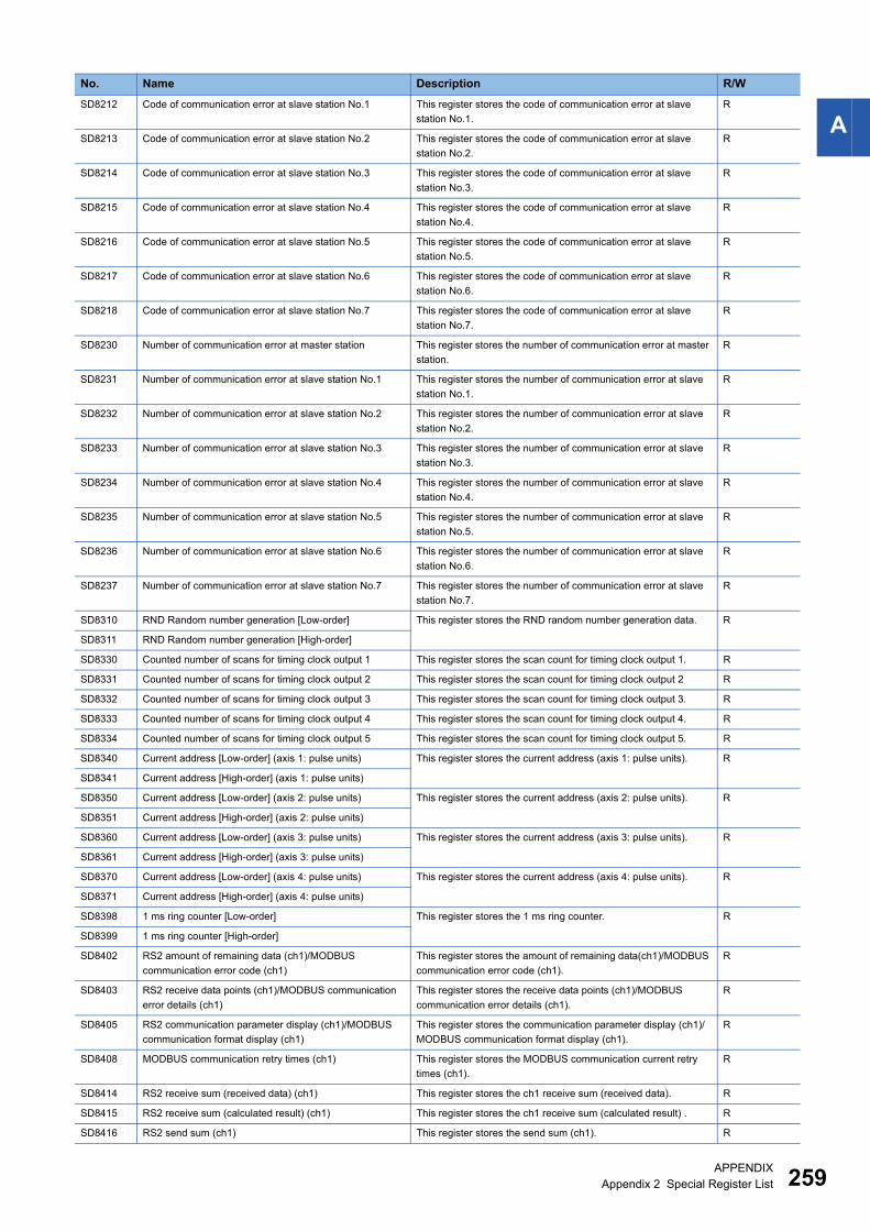
APPENDIX
Appendix 2 Special Register List 259
ASD8212 Code of communication error at slave station No.1 This register stores the code of communication error at slave
station No.1.
R
SD8213 Code of communication error at slave station No.2 This register stores the code of communication error at slave
station No.2.
R
SD8214 Code of communication error at slave station No.3 This register stores the code of communication error at slave
station No.3.
R
SD8215 Code of communication error at slave station No.4 This register stores the code of communication error at slave
station No.4.
R
SD8216 Code of communication error at slave station No.5 This register stores the code of communication error at slave
station No.5.
R
SD8217 Code of communication error at slave station No.6 This register stores the code of communication error at slave
station No.6.
R
SD8218 Code of communication error at slave station No.7 This register stores the code of communication error at slave
station No.7.
R
SD8230 Number of communication error at master station This register stores the number of communication error at master
station.
R
SD8231 Number of communication error at slave station No.1 This register stores the number of communication error at slave
station No.1.
R
SD8232 Number of communication error at slave station No.2 This register stores the number of communication error at slave
station No.2.
R
SD8233 Number of communication error at slave station No.3 This register stores the number of communication error at slave
station No.3.
R
SD8234 Number of communication error at slave station No.4 This register stores the number of communication error at slave
station No.4.
R
SD8235 Number of communication error at slave station No.5 This register stores the number of communication error at slave
station No.5.
R
SD8236 Number of communication error at slave station No.6 This register stores the number of communication error at slave
station No.6.
R
SD8237 Number of communication error at slave station No.7 This register stores the number of communication error at slave
station No.7.
R
SD8310 RND Random number generation [Low-order] This register stores the RND random number generation data. R
SD8311 RND Random number generation [High-order]
SD8330 Counted number of scans for timing clock output 1 This register stores the scan count for timing clock output 1. R
SD8331 Counted number of scans for timing clock output 2 This register stores the scan count for timing clock output 2 R
SD8332 Counted number of scans for timing clock output 3 This register stores the scan count for timing clock output 3. R
SD8333 Counted number of scans for timing clock output 4 This register stores the scan count for timing clock output 4. R
SD8334 Counted number of scans for timing clock output 5 This register stores the scan count for timing clock output 5. R
SD8340 Current address [Low-order] (axis 1: pulse units) This register stores the current address (axis 1: pulse units). R
SD8341 Current address [High-order] (axis 1: pulse units)
SD8350 Current address [Low-order] (axis 2: pulse units) This register stores the current address (axis 2: pulse units). R
SD8351 Current address [High-order] (axis 2: pulse units)
SD8360 Current address [Low-order] (axis 3: pulse units) This register stores the current address (axis 3: pulse units). R
SD8361 Current address [High-order] (axis 3: pulse units)
SD8370 Current address [Low-order] (axis 4: pulse units) This register stores the current address (axis 4: pulse units). R
SD8371 Current address [High-order] (axis 4: pulse units)
SD8398 1 ms ring counter [Low-order] This register stores the 1 ms ring counter. R
SD8399 1 ms ring counter [High-order]
SD8402 RS2 amount of remaining data (ch1)/MODBUS
communication error code (ch1)
This register stores the amount of remaining data(ch1)/MODBUS
communication error code (ch1).
R
SD8403 RS2 receive data points (ch1)/MODBUS communication
error details (ch1)
This register stores the receive data points (ch1)/MODBUS
communication error details (ch1).
R
SD8405 RS2 communication parameter display (ch1)/MODBUS
communication format display (ch1)
This register stores the communication parameter display (ch1)/
MODBUS communication format display (ch1).
R
SD8408 MODBUS communication retry times (ch1) This register stores the MODBUS communication current retry
times (ch1).
R
SD8414 RS2 receive sum (received data) (ch1) This register stores the ch1 receive sum (received data). R
SD8415 RS2 receive sum (calculated result) (ch1) This register stores the ch1 receive sum (calculated result) . R
SD8416 RS2 send sum (ch1) This register stores the send sum (ch1). R
No. Name Description R/W
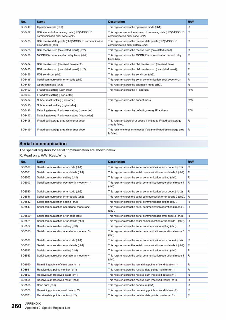
260APPENDIX
Appendix 2 Special Register List
Serial communication
The special registers for serial communication are shown below.
R: Read only, R/W: Read/Write
SD8419 Operation mode (ch1) This register stores the operation mode (ch1). R
SD8422 RS2 amount of remaining data (ch2)/MODBUS
communication error code (ch2)
This register stores the amount of remaining data (ch2)/MODBUS
communication error code (ch2).
R
SD8423 RS2 receive data points (ch2)/MODBUS communication
error details (ch2)
This register stores the receive data points (ch2)/MODBUS
communication error details (ch2).
R
SD8425 RS2 receive sum (calculated result) (ch2) This register stores the receive sum (calculated result). R
SD8428 MODBUS communication retry times (ch2) This register stores the MODBUS communication current retry
times (ch2).
R
SD8434 RS2 receive sum (received data) (ch2) This register stores the ch2 receive sum (received data). R
SD8435 RS2 receive sum (calculated result) (ch2) This register stores the ch2 receive sum (calculated result). R
SD8436 RS2 send sum (ch2) This register stores the send sum (ch2). R
SD8438 Serial communication error code (ch2) This register stores the serial communication error code (ch2). R
SD8439 Operation mode (ch2) This register stores the operation mode (ch2). R
SD8492 IP address setting [Low-order] This register stores the IP address. R/W
SD8493 IP address setting [High-order]
SD8494 Subnet mask setting [Low-order] This register stores the subnet mask. R/W
SD8495 Subnet mask setting [High-order]
SD8496 Default gateway IP address setting [Low-order] This register stores the default gateway IP address. R/W
SD8497 Default gateway IP address setting [High-order]
SD8498 IP address storage area write error code This register stores error codes if writing to IP address storage
area is failed.
R
SD8499 IP address storage area clear error code This register stores error codes if clear to IP address storage area
is failed.
R
No. Name Description R/W
SD8500 Serial communication error code (ch1) This register stores the serial communication error code 1 (ch1). R
SD8501 Serial communication error details (ch1) This register stores the serial communication error details 1 (ch1). R
SD8502 Serial communication setting (ch1) This register stores the serial communication setting (ch1). R
SD8503 Serial communication operational mode (ch1) This register stores the serial communication operational mode 1
(ch1).
R
SD8510 Serial communication error code (ch2) This register stores the serial communication error code 2 (ch2). R
SD8511 Serial communication error details (ch2) This register stores the serial communication error details 2 (ch2). R
SD8512 Serial communication setting (ch2) This register stores the serial communication setting (ch2). R
SD8513 Serial communication operational mode (ch2) This register stores the serial communication operational mode 2
(ch2).
R
SD8520 Serial communication error code (ch3) This register stores the serial communication error code 3 (ch3). R
SD8521 Serial communication error details (ch3) This register stores the serial communication error details 3 (ch3). R
SD8522 Serial communication setting (ch3) This register stores the serial communication setting (ch3). R
SD8523 Serial communication operational mode (ch3) This register stores the serial communication operational mode 3
(ch3).
R
SD8530 Serial communication error code (ch4) This register stores the serial communication error code 4 (ch4). R
SD8531 Serial communication error details (ch4) This register stores the serial communication error details 4 (ch4). R
SD8532 Serial communication setting (ch4) This register stores the serial communication setting (ch4). R
SD8533 Serial communication operational mode (ch4) This register stores the serial communication operational mode 4
(ch4).
R
SD8560 Remaining points of send data (ch1) This register stores the remaining points of send data (ch1). R
SD8561 Receive data points monitor (ch1) This register stores the receive data points monitor (ch1). R
SD8563 Receive sum (received data) (ch1) This register stores the receive sum (received data) (ch1). R
SD8564 Receive sum (received result) (ch1) This register stores the receive sum (received result) (ch1). R
SD8565 Send sum (ch1) This register stores the send sum (ch1). R
SD8570 Remaining points of send data (ch2) This register stores the remaining points of send data (ch2). R
SD8571 Receive data points monitor (ch2) This register stores the receive data points monitor (ch2). R
No. Name Description R/W
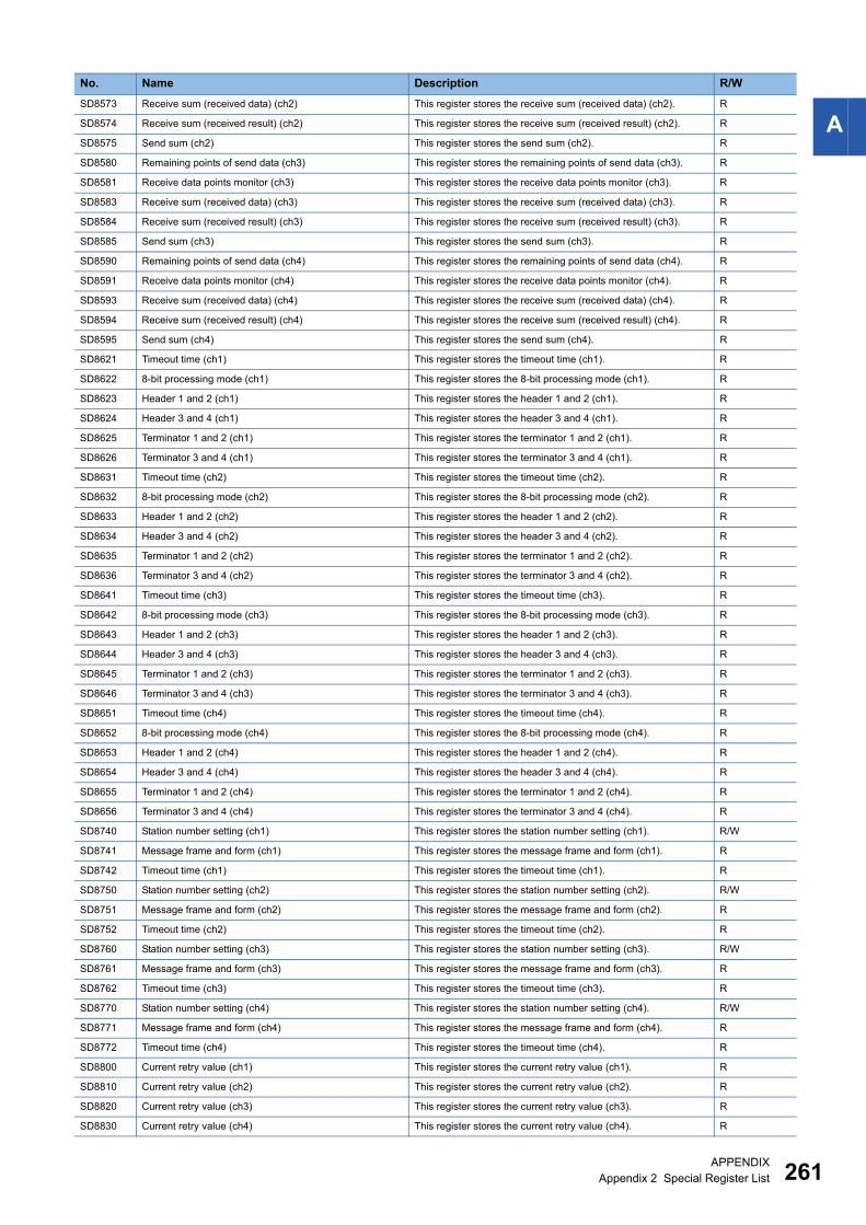
APPENDIX
Appendix 2 Special Register List 261
ASD8573 Receive sum (received data) (ch2) This register stores the receive sum (received data) (ch2). R
SD8574 Receive sum (received result) (ch2) This register stores the receive sum (received result) (ch2). R
SD8575 Send sum (ch2) This register stores the send sum (ch2). R
SD8580 Remaining points of send data (ch3) This register stores the remaining points of send data (ch3). R
SD8581 Receive data points monitor (ch3) This register stores the receive data points monitor (ch3). R
SD8583 Receive sum (received data) (ch3) This register stores the receive sum (received data) (ch3). R
SD8584 Receive sum (received result) (ch3) This register stores the receive sum (received result) (ch3). R
SD8585 Send sum (ch3) This register stores the send sum (ch3). R
SD8590 Remaining points of send data (ch4) This register stores the remaining points of send data (ch4). R
SD8591 Receive data points monitor (ch4) This register stores the receive data points monitor (ch4). R
SD8593 Receive sum (received data) (ch4) This register stores the receive sum (received data) (ch4). R
SD8594 Receive sum (received result) (ch4) This register stores the receive sum (received result) (ch4). R
SD8595 Send sum (ch4) This register stores the send sum (ch4). R
SD8621 Timeout time (ch1) This register stores the timeout time (ch1). R
SD8622 8-bit processing mode (ch1) This register stores the 8-bit processing mode (ch1). R
SD8623 Header 1 and 2 (ch1) This register stores the header 1 and 2 (ch1). R
SD8624 Header 3 and 4 (ch1) This register stores the header 3 and 4 (ch1). R
SD8625 Terminator 1 and 2 (ch1) This register stores the terminator 1 and 2 (ch1). R
SD8626 Terminator 3 and 4 (ch1) This register stores the terminator 3 and 4 (ch1). R
SD8631 Timeout time (ch2) This register stores the timeout time (ch2). R
SD8632 8-bit processing mode (ch2) This register stores the 8-bit processing mode (ch2). R
SD8633 Header 1 and 2 (ch2) This register stores the header 1 and 2 (ch2). R
SD8634 Header 3 and 4 (ch2) This register stores the header 3 and 4 (ch2). R
SD8635 Terminator 1 and 2 (ch2) This register stores the terminator 1 and 2 (ch2). R
SD8636 Terminator 3 and 4 (ch2) This register stores the terminator 3 and 4 (ch2). R
SD8641 Timeout time (ch3) This register stores the timeout time (ch3). R
SD8642 8-bit processing mode (ch3) This register stores the 8-bit processing mode (ch3). R
SD8643 Header 1 and 2 (ch3) This register stores the header 1 and 2 (ch3). R
SD8644 Header 3 and 4 (ch3) This register stores the header 3 and 4 (ch3). R
SD8645 Terminator 1 and 2 (ch3) This register stores the terminator 1 and 2 (ch3). R
SD8646 Terminator 3 and 4 (ch3) This register stores the terminator 3 and 4 (ch3). R
SD8651 Timeout time (ch4) This register stores the timeout time (ch4). R
SD8652 8-bit processing mode (ch4) This register stores the 8-bit processing mode (ch4). R
SD8653 Header 1 and 2 (ch4) This register stores the header 1 and 2 (ch4). R
SD8654 Header 3 and 4 (ch4) This register stores the header 3 and 4 (ch4). R
SD8655 Terminator 1 and 2 (ch4) This register stores the terminator 1 and 2 (ch4). R
SD8656 Terminator 3 and 4 (ch4) This register stores the terminator 3 and 4 (ch4). R
SD8740 Station number setting (ch1) This register stores the station number setting (ch1). R/W
SD8741 Message frame and form (ch1) This register stores the message frame and form (ch1). R
SD8742 Timeout time (ch1) This register stores the timeout time (ch1). R
SD8750 Station number setting (ch2) This register stores the station number setting (ch2). R/W
SD8751 Message frame and form (ch2) This register stores the message frame and form (ch2). R
SD8752 Timeout time (ch2) This register stores the timeout time (ch2). R
SD8760 Station number setting (ch3) This register stores the station number setting (ch3). R/W
SD8761 Message frame and form (ch3) This register stores the message frame and form (ch3). R
SD8762 Timeout time (ch3) This register stores the timeout time (ch3). R
SD8770 Station number setting (ch4) This register stores the station number setting (ch4). R/W
SD8771 Message frame and form (ch4) This register stores the message frame and form (ch4). R
SD8772 Timeout time (ch4) This register stores the timeout time (ch4). R
SD8800 Current retry value (ch1) This register stores the current retry value (ch1). R
SD8810 Current retry value (ch2) This register stores the current retry value (ch2). R
SD8820 Current retry value (ch3) This register stores the current retry value (ch3). R
SD8830 Current retry value (ch4) This register stores the current retry value (ch4). R
No. Name Description R/W
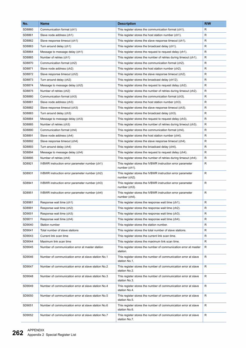
262APPENDIX
Appendix 2 Special Register List
SD8860 Communication format (ch1) This register stores the communication format (ch1). R
SD8861 Slave node address (ch1) This register stores the host station number (ch1). R
SD8862 Slave response timeout (ch1) This register stores the slave response timeout (ch1). R
SD8863 Turn around delay (ch1) This register stores the broadcast delay (ch1). R
SD8864 Message to message delay (ch1) This register stores the request to request delay (ch1). R
SD8865 Number of retries (ch1) This register stores the number of retries during timeout (ch1). R
SD8870 Communication format (ch2) This register stores the communication format (ch2). R
SD8871 Slave node address (ch2) This register stores the host station number (ch2). R
SD8872 Slave response timeout (ch2) This register stores the slave response timeout (ch2). R
SD8873 Turn around delay (ch2) This register stores the broadcast delay (ch12). R
SD8874 Message to message delay (ch2) This register stores the request to request delay (ch2). R
SD8875 Number of retries (ch2) This register stores the number of retries during timeout (ch2). R
SD8880 Communication format (ch3) This register stores the communication format (ch3). R
SD8881 Slave node address (ch3) This register stores the host station number (ch3). R
SD8882 Slave response timeout (ch3) This register stores the slave response timeout (ch3). R
SD8883 Turn around delay (ch3) This register stores the broadcast delay (ch3). R
SD8884 Message to message delay (ch3) This register stores the request to request delay (ch3). R
SD8885 Number of retries (ch3) This register stores the number of retries during timeout (ch3). R
SD8890 Communication format (ch4) This register stores the communication format (ch4). R
SD8891 Slave node address (ch4) This register stores the host station number (ch4). R
SD8892 Slave response timeout (ch4) This register stores the slave response timeout (ch4). R
SD8893 Turn around delay (ch4) This register stores the broadcast delay (ch4). R
SD8894 Message to message delay (ch4) This register stores the request to request delay (ch4). R
SD8895 Number of retries (ch4) This register stores the number of retries during timeout (ch4). R
SD8921 IVBWR instruction error parameter number (ch1) This register stores the IVBWR instruction error parameter
number (ch1).
R
SD8931 IVBWR instruction error parameter number (ch2) This register stores the IVBWR instruction error parameter
number (ch2).
R
SD8941 IVBWR instruction error parameter number (ch3) This register stores the IVBWR instruction error parameter
number (ch3).
R
SD8951 IVBWR instruction error parameter number (ch4) This register stores the IVBWR instruction error parameter
number (ch4).
R
SD8981 Response wait time (ch1) This register stores the response wait time (ch1). R
SD8991 Response wait time (ch2) This register stores the response wait time (ch2). R
SD9001 Response wait time (ch3) This register stores the response wait time (ch3). R
SD9011 Response wait time (ch4) This register stores the response wait time (ch4). R
SD9040 Station number This register stores the station number. R
SD9041 Total number of slave stations This register stores the total number of slave stations. R
SD9043 Current link scan time This register stores the current link scan time. R
SD9044 Maximum link scan time This register stores the maximum link scan time. R
SD9045 Number of communication error at master station This register stores the number of communication error at master
station.
R
SD9046 Number of communication error at slave station No.1 This register stores the number of communication error at slave
station No.1.
R
SD9047 Number of communication error at slave station No.2 This register stores the number of communication error at slave
station No.2.
R
SD9048 Number of communication error at slave station No.3 This register stores the number of communication error at slave
station No.3.
R
SD9049 Number of communication error at slave station No.4 This register stores the number of communication error at slave
station No.4.
R
SD9050 Number of communication error at slave station No.5 This register stores the number of communication error at slave
station No.5.
R
SD9051 Number of communication error at slave station No.6 This register stores the number of communication error at slave
station No.6.
R
SD9052 Number of communication error at slave station No.7 This register stores the number of communication error at slave
station No.7.
R
No. Name Description R/W
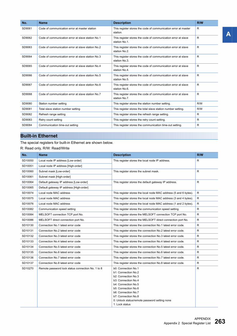
APPENDIX
Appendix 2 Special Register List 263
A
Built-in Ethernet
The special registers for built-in Ethernet are shown below.
R: Read only, R/W: Read/Write
SD9061 Code of communication error at master station This register stores the code of communication error at master
station.
R
SD9062 Code of communication error at slave station No.1 This register stores the code of communication error at slave
station No.1.
R
SD9063 Code of communication error at slave station No.2 This register stores the code of communication error at slave
station No.2.
R
SD9064 Code of communication error at slave station No.3 This register stores the code of communication error at slave
station No.3.
R
SD9065 Code of communication error at slave station No.4 This register stores the code of communication error at slave
station No.4.
R
SD9066 Code of communication error at slave station No.5 This register stores the code of communication error at slave
station No.5.
R
SD9067 Code of communication error at slave station No.6 This register stores the code of communication error at slave
station No.6.
R
SD9068 Code of communication error at slave station No.7 This register stores the code of communication error at slave
station No.7.
R
SD9080 Station number setting This register stores the station number setting. R/W
SD9081 Total slave station number setting This register stores the total slave station number setting. R/W
SD9082 Refresh range setting This register stores the refresh range setting. R
SD9083 Retry count setting This register stores the retry count setting. R
SD9084 Communication time-out setting This register stores the communication time-out setting. R
No. Name Description R/W
SD10050 Local node IP address [Low-order] This register stores the local node IP address. R
SD10051 Local node IP address [High-order]
SD10060 Subnet mask [Low-order] This register stores the subnet mask. R
SD10061 Subnet mask [High-order]
SD10064 Default gateway IP address [Low-order] This register stores the default gateway IP address. R
SD10065 Default gateway IP address [High-order]
SD10074 Local node MAC address This register stores the local node MAC address (5 and 6 bytes). R
SD10075 Local node MAC address This register stores the local node MAC address (3 and 4 bytes). R
SD10076 Local node MAC address This register stores the local node MAC address (1 and 2 bytes). R
SD10082 Communication speed setting This register stores the communication speed setting. R
SD10084 MELSOFT connection TCP port No. This register stores the MELSOFT connection TCP port No. R
SD10086 MELSOFT direct connection port No. This register stores the MELSOFT direct connection port No. R
SD10130 Connection No.1 latest error code This register stores the connection No.1 latest error code. R
SD10131 Connection No.2 latest error code This register stores the connection No.2 latest error code. R
SD10132 Connection No.3 latest error code This register stores the connection No.3 latest error code. R
SD10133 Connection No.4 latest error code This register stores the connection No.4 latest error code. R
SD10134 Connection No.5 latest error code This register stores the connection No.5 latest error code. R
SD10135 Connection No.6 latest error code This register stores the connection No.6 latest error code. R
SD10136 Connection No.7 latest error code This register stores the connection No.7 latest error code. R
SD10137 Connection No.8 latest error code This register stores the connection No.8 latest error code. R
SD10270 Remote password lock status connection No. 1 to 8 b0: Connection No.1
b1: Connection No.2
b2: Connection No.3
b3: Connection No.4
b4: Connection No.5
b5: Connection No.6
b6: Connection No.7
b7: Connection No.8
0: Unlock status/remote password setting none
1: Lock status
R
No. Name Description R/W
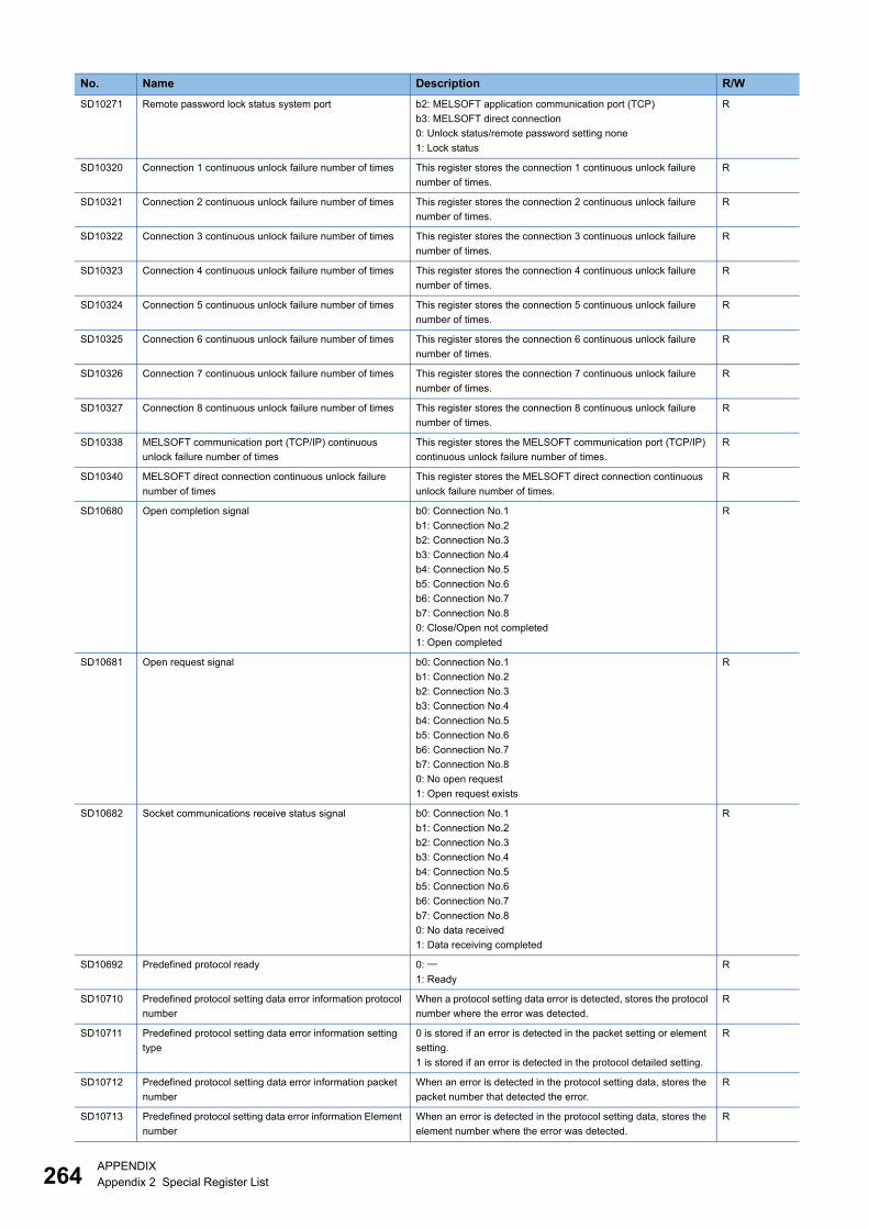
264APPENDIX
Appendix 2 Special Register List
SD10271 Remote password lock status system port b2: MELSOFT application communication port (TCP)
b3: MELSOFT direct connection
0: Unlock status/remote password setting none
1: Lock status
R
SD10320 Connection 1 continuous unlock failure number of times This register stores the connection 1 continuous unlock failure
number of times.
R
SD10321 Connection 2 continuous unlock failure number of times This register stores the connection 2 continuous unlock failure
number of times.
R
SD10322 Connection 3 continuous unlock failure number of times This register stores the connection 3 continuous unlock failure
number of times.
R
SD10323 Connection 4 continuous unlock failure number of times This register stores the connection 4 continuous unlock failure
number of times.
R
SD10324 Connection 5 continuous unlock failure number of times This register stores the connection 5 continuous unlock failure
number of times.
R
SD10325 Connection 6 continuous unlock failure number of times This register stores the connection 6 continuous unlock failure
number of times.
R
SD10326 Connection 7 continuous unlock failure number of times This register stores the connection 7 continuous unlock failure
number of times.
R
SD10327 Connection 8 continuous unlock failure number of times This register stores the connection 8 continuous unlock failure
number of times.
R
SD10338 MELSOFT communication port (TCP/IP) continuous
unlock failure number of times
This register stores the MELSOFT communication port (TCP/IP)
continuous unlock failure number of times.
R
SD10340 MELSOFT direct connection continuous unlock failure
number of times
This register stores the MELSOFT direct connection continuous
unlock failure number of times.
R
SD10680 Open completion signal b0: Connection No.1
b1: Connection No.2
b2: Connection No.3
b3: Connection No.4
b4: Connection No.5
b5: Connection No.6
b6: Connection No.7
b7: Connection No.8
0: Close/Open not completed
1: Open completed
R
SD10681 Open request signal b0: Connection No.1
b1: Connection No.2
b2: Connection No.3
b3: Connection No.4
b4: Connection No.5
b5: Connection No.6
b6: Connection No.7
b7: Connection No.8
0: No open request
1: Open request exists
R
SD10682 Socket communications receive status signal b0: Connection No.1
b1: Connection No.2
b2: Connection No.3
b3: Connection No.4
b4: Connection No.5
b5: Connection No.6
b6: Connection No.7
b7: Connection No.8
0: No data received
1: Data receiving completed
R
SD10692 Predefined protocol ready 0:
1: Ready
R
SD10710 Predefined protocol setting data error information protocol
number
When a protocol setting data error is detected, stores the protocol
number where the error was detected.
R
SD10711 Predefined protocol setting data error information setting
type
0 is stored if an error is detected in the packet setting or element
setting.
1 is stored if an error is detected in the protocol detailed setting.
R
SD10712 Predefined protocol setting data error information packet
number
When an error is detected in the protocol setting data, stores the
packet number that detected the error.
R
SD10713 Predefined protocol setting data error information Element
number
When an error is detected in the protocol setting data, stores the
element number where the error was detected.
R
No. Name Description R/W
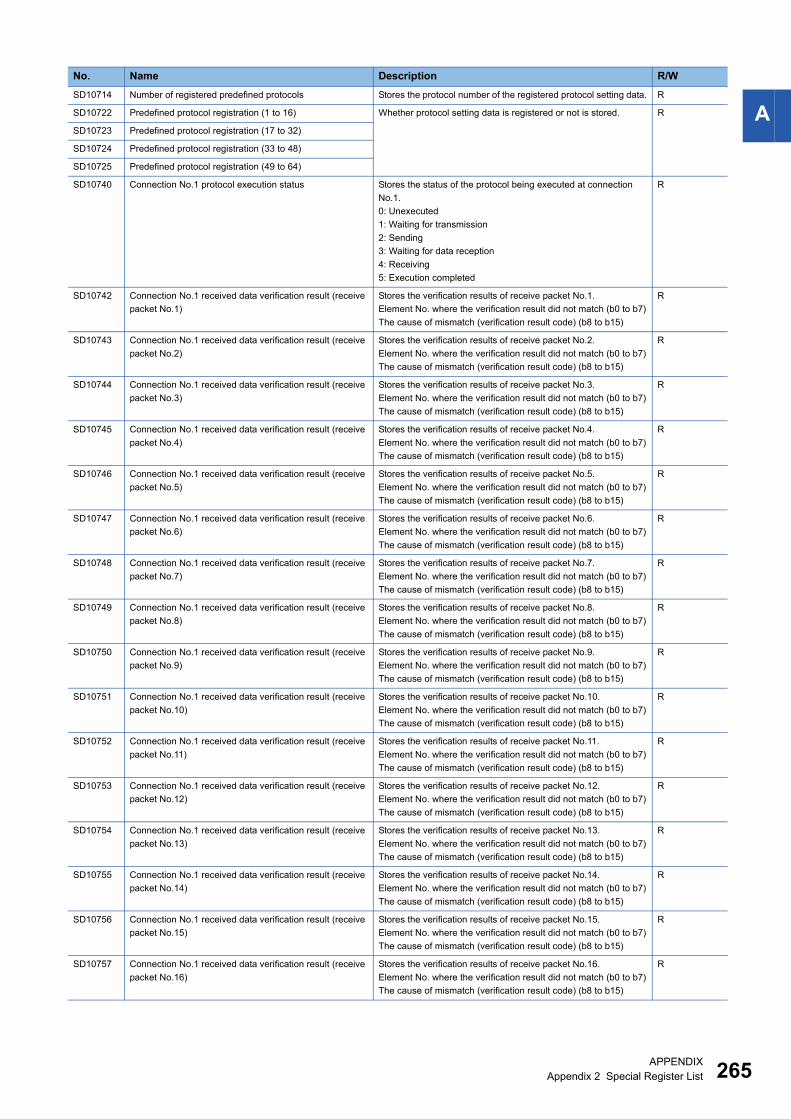
APPENDIX
Appendix 2 Special Register List 265
ASD10714 Number of registered predefined protocols Stores the protocol number of the registered protocol setting data. R
SD10722 Predefined protocol registration (1 to 16) Whether protocol setting data is registered or not is stored. R
SD10723 Predefined protocol registration (17 to 32)
SD10724 Predefined protocol registration (33 to 48)
SD10725 Predefined protocol registration (49 to 64)
SD10740 Connection No.1 protocol execution status Stores the status of the protocol being executed at connection
No.1.
0: Unexecuted
1: Waiting for transmission
2: Sending
3: Waiting for data reception
4: Receiving
5: Execution completed
R
SD10742 Connection No.1 received data verification result (receive
packet No.1)
Stores the verification results of receive packet No.1.
Element No. where the verification result did not match (b0 to b7)
The cause of mismatch (verification result code) (b8 to b15)
R
SD10743 Connection No.1 received data verification result (receive
packet No.2)
Stores the verification results of receive packet No.2.
Element No. where the verification result did not match (b0 to b7)
The cause of mismatch (verification result code) (b8 to b15)
R
SD10744 Connection No.1 received data verification result (receive
packet No.3)
Stores the verification results of receive packet No.3.
Element No. where the verification result did not match (b0 to b7)
The cause of mismatch (verification result code) (b8 to b15)
R
SD10745 Connection No.1 received data verification result (receive
packet No.4)
Stores the verification results of receive packet No.4.
Element No. where the verification result did not match (b0 to b7)
The cause of mismatch (verification result code) (b8 to b15)
R
SD10746 Connection No.1 received data verification result (receive
packet No.5)
Stores the verification results of receive packet No.5.
Element No. where the verification result did not match (b0 to b7)
The cause of mismatch (verification result code) (b8 to b15)
R
SD10747 Connection No.1 received data verification result (receive
packet No.6)
Stores the verification results of receive packet No.6.
Element No. where the verification result did not match (b0 to b7)
The cause of mismatch (verification result code) (b8 to b15)
R
SD10748 Connection No.1 received data verification result (receive
packet No.7)
Stores the verification results of receive packet No.7.
Element No. where the verification result did not match (b0 to b7)
The cause of mismatch (verification result code) (b8 to b15)
R
SD10749 Connection No.1 received data verification result (receive
packet No.8)
Stores the verification results of receive packet No.8.
Element No. where the verification result did not match (b0 to b7)
The cause of mismatch (verification result code) (b8 to b15)
R
SD10750 Connection No.1 received data verification result (receive
packet No.9)
Stores the verification results of receive packet No.9.
Element No. where the verification result did not match (b0 to b7)
The cause of mismatch (verification result code) (b8 to b15)
R
SD10751 Connection No.1 received data verification result (receive
packet No.10)
Stores the verification results of receive packet No.10.
Element No. where the verification result did not match (b0 to b7)
The cause of mismatch (verification result code) (b8 to b15)
R
SD10752 Connection No.1 received data verification result (receive
packet No.11)
Stores the verification results of receive packet No.11.
Element No. where the verification result did not match (b0 to b7)
The cause of mismatch (verification result code) (b8 to b15)
R
SD10753 Connection No.1 received data verification result (receive
packet No.12)
Stores the verification results of receive packet No.12.
Element No. where the verification result did not match (b0 to b7)
The cause of mismatch (verification result code) (b8 to b15)
R
SD10754 Connection No.1 received data verification result (receive
packet No.13)
Stores the verification results of receive packet No.13.
Element No. where the verification result did not match (b0 to b7)
The cause of mismatch (verification result code) (b8 to b15)
R
SD10755 Connection No.1 received data verification result (receive
packet No.14)
Stores the verification results of receive packet No.14.
Element No. where the verification result did not match (b0 to b7)
The cause of mismatch (verification result code) (b8 to b15)
R
SD10756 Connection No.1 received data verification result (receive
packet No.15)
Stores the verification results of receive packet No.15.
Element No. where the verification result did not match (b0 to b7)
The cause of mismatch (verification result code) (b8 to b15)
R
SD10757 Connection No.1 received data verification result (receive
packet No.16)
Stores the verification results of receive packet No.16.
Element No. where the verification result did not match (b0 to b7)
The cause of mismatch (verification result code) (b8 to b15)
R
No. Name Description R/W
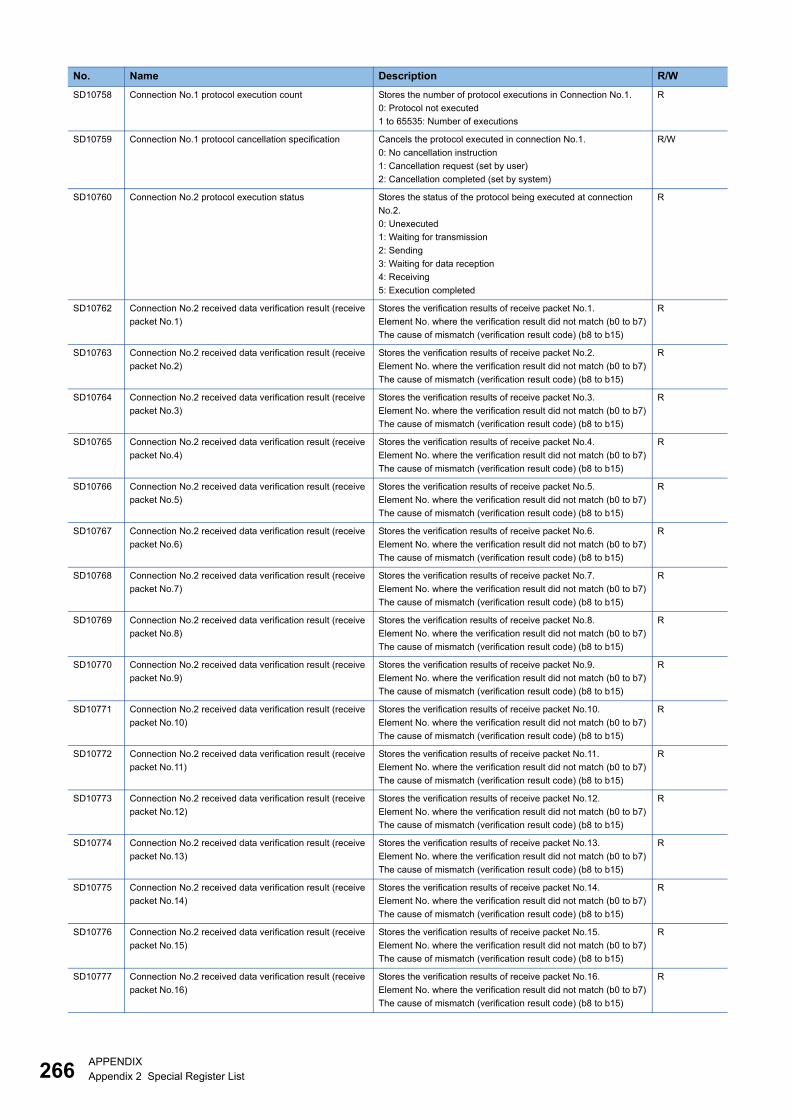
266APPENDIX
Appendix 2 Special Register List
SD10758 Connection No.1 protocol execution count Stores the number of protocol executions in Connection No.1.
0: Protocol not executed
1 to 65535: Number of executions
R
SD10759 Connection No.1 protocol cancellation specification Cancels the protocol executed in connection No.1.
0: No cancellation instruction
1: Cancellation request (set by user)
2: Cancellation completed (set by system)
R/W
SD10760 Connection No.2 protocol execution status Stores the status of the protocol being executed at connection
No.2.
0: Unexecuted
1: Waiting for transmission
2: Sending
3: Waiting for data reception
4: Receiving
5: Execution completed
R
SD10762 Connection No.2 received data verification result (receive
packet No.1)
Stores the verification results of receive packet No.1.
Element No. where the verification result did not match (b0 to b7)
The cause of mismatch (verification result code) (b8 to b15)
R
SD10763 Connection No.2 received data verification result (receive
packet No.2)
Stores the verification results of receive packet No.2.
Element No. where the verification result did not match (b0 to b7)
The cause of mismatch (verification result code) (b8 to b15)
R
SD10764 Connection No.2 received data verification result (receive
packet No.3)
Stores the verification results of receive packet No.3.
Element No. where the verification result did not match (b0 to b7)
The cause of mismatch (verification result code) (b8 to b15)
R
SD10765 Connection No.2 received data verification result (receive
packet No.4)
Stores the verification results of receive packet No.4.
Element No. where the verification result did not match (b0 to b7)
The cause of mismatch (verification result code) (b8 to b15)
R
SD10766 Connection No.2 received data verification result (receive
packet No.5)
Stores the verification results of receive packet No.5.
Element No. where the verification result did not match (b0 to b7)
The cause of mismatch (verification result code) (b8 to b15)
R
SD10767 Connection No.2 received data verification result (receive
packet No.6)
Stores the verification results of receive packet No.6.
Element No. where the verification result did not match (b0 to b7)
The cause of mismatch (verification result code) (b8 to b15)
R
SD10768 Connection No.2 received data verification result (receive
packet No.7)
Stores the verification results of receive packet No.7.
Element No. where the verification result did not match (b0 to b7)
The cause of mismatch (verification result code) (b8 to b15)
R
SD10769 Connection No.2 received data verification result (receive
packet No.8)
Stores the verification results of receive packet No.8.
Element No. where the verification result did not match (b0 to b7)
The cause of mismatch (verification result code) (b8 to b15)
R
SD10770 Connection No.2 received data verification result (receive
packet No.9)
Stores the verification results of receive packet No.9.
Element No. where the verification result did not match (b0 to b7)
The cause of mismatch (verification result code) (b8 to b15)
R
SD10771 Connection No.2 received data verification result (receive
packet No.10)
Stores the verification results of receive packet No.10.
Element No. where the verification result did not match (b0 to b7)
The cause of mismatch (verification result code) (b8 to b15)
R
SD10772 Connection No.2 received data verification result (receive
packet No.11)
Stores the verification results of receive packet No.11.
Element No. where the verification result did not match (b0 to b7)
The cause of mismatch (verification result code) (b8 to b15)
R
SD10773 Connection No.2 received data verification result (receive
packet No.12)
Stores the verification results of receive packet No.12.
Element No. where the verification result did not match (b0 to b7)
The cause of mismatch (verification result code) (b8 to b15)
R
SD10774 Connection No.2 received data verification result (receive
packet No.13)
Stores the verification results of receive packet No.13.
Element No. where the verification result did not match (b0 to b7)
The cause of mismatch (verification result code) (b8 to b15)
R
SD10775 Connection No.2 received data verification result (receive
packet No.14)
Stores the verification results of receive packet No.14.
Element No. where the verification result did not match (b0 to b7)
The cause of mismatch (verification result code) (b8 to b15)
R
SD10776 Connection No.2 received data verification result (receive
packet No.15)
Stores the verification results of receive packet No.15.
Element No. where the verification result did not match (b0 to b7)
The cause of mismatch (verification result code) (b8 to b15)
R
SD10777 Connection No.2 received data verification result (receive
packet No.16)
Stores the verification results of receive packet No.16.
Element No. where the verification result did not match (b0 to b7)
The cause of mismatch (verification result code) (b8 to b15)
R
No. Name Description R/W

APPENDIX
Appendix 2 Special Register List 267
ASD10778 Connection No.2 protocol execution count Stores the number of protocol executions in connection No.2.
0: Protocol not executed
1 to 65535: Number of executions
R
SD10779 Connection No.2 protocol cancellation specification Cancels the protocol executed in connection No.2.
0: No cancellation instruction
1: Cancellation request (set by user)
2: Cancellation completed (set by system)
R/W
SD10780 Connection No.3 protocol execution status Stores the status of the protocol being executed at connection
No.3.
0: Unexecuted
1: Waiting for transmission
2: Sending
3: Waiting for data reception
4: Receiving
5: Execution completed
R
SD10782 Connection No.3 received data verification result (receive
packet No.1)
Stores the verification results of receive packet No.1.
Element No. where the verification result did not match (b0 to b7)
The cause of mismatch (verification result code) (b8 to b15)
R
SD10783 Connection No.3 received data verification result (receive
packet No.2)
Stores the verification results of receive packet No.2.
Element No. where the verification result did not match (b0 to b7)
The cause of mismatch (verification result code) (b8 to b15)
R
SD10784 Connection No.3 received data verification result (receive
packet No.3)
Stores the verification results of receive packet No.3.
Element No. where the verification result did not match (b0 to b7)
The cause of mismatch (verification result code) (b8 to b15)
R
SD10785 Connection No.3 received data verification result (receive
packet No.4)
Stores the verification results of receive packet No.4.
Element No. where the verification result did not match (b0 to b7)
The cause of mismatch (verification result code) (b8 to b15)
R
SD10786 Connection No.3 received data verification result (receive
packet No.5)
Stores the verification results of receive packet No.5.
Element No. where the verification result did not match (b0 to b7)
The cause of mismatch (verification result code) (b8 to b15)
R
SD10787 Connection No.3 received data verification result (receive
packet No.6)
Stores the verification results of receive packet No.6.
Element No. where the verification result did not match (b0 to b7)
The cause of mismatch (verification result code) (b8 to b15)
R
SD10788 Connection No.3 received data verification result (receive
packet No.7)
Stores the verification results of receive packet No.7.
Element No. where the verification result did not match (b0 to b7)
The cause of mismatch (verification result code) (b8 to b15)
R
SD10789 Connection No.3 received data verification result (receive
packet No.8)
Stores the verification results of receive packet No.8.
Element No. where the verification result did not match (b0 to b7)
The cause of mismatch (verification result code) (b8 to b15)
R
SD10790 Connection No.3 received data verification result (receive
packet No.9)
Stores the verification results of receive packet No.9.
Element No. where the verification result did not match (b0 to b7)
The cause of mismatch (verification result code) (b8 to b15)
R
SD10791 Connection No.3 received data verification result (receive
packet No.10)
Stores the verification results of receive packet No.10.
Element No. where the verification result did not match (b0 to b7)
The cause of mismatch (verification result code) (b8 to b15)
R
SD10792 Connection No.3 received data verification result (receive
packet No.11)
Stores the verification results of receive packet No.11.
Element No. where the verification result did not match (b0 to b7)
The cause of mismatch (verification result code) (b8 to b15)
R
SD10793 Connection No.3 received data verification result (receive
packet No.12)
Stores the verification results of receive packet No.12.
Element No. where the verification result did not match (b0 to b7)
The cause of mismatch (verification result code) (b8 to b15)
R
SD10794 Connection No.3 received data verification result (receive
packet No.13)
Stores the verification results of receive packet No.13.
Element No. where the verification result did not match (b0 to b7)
The cause of mismatch (verification result code) (b8 to b15)
R
SD10795 Connection No.3 received data verification result (receive
packet No.14)
Stores the verification results of receive packet No.14.
Element No. where the verification result did not match (b0 to b7)
The cause of mismatch (verification result code) (b8 to b15)
R
SD10796 Connection No.3 received data verification result (receive
packet No.15)
Stores the verification results of receive packet No.15.
Element No. where the verification result did not match (b0 to b7)
The cause of mismatch (verification result code) (b8 to b15)
R
SD10797 Connection No.3 received data verification result (receive
packet No.16)
Stores the verification results of receive packet No.16.
Element No. where the verification result did not match (b0 to b7)
The cause of mismatch (verification result code) (b8 to b15)
R
No. Name Description R/W

268APPENDIX
Appendix 2 Special Register List
SD10798 Connection No.3 protocol execution count Stores the number of protocol executions in connection No.3.
0: Protocol not executed
1 to 65535: Number of executions
R
SD10799 Connection No.3 protocol cancellation specification Cancels the protocol executed in connection No.3.
0: No cancellation instruction
1: Cancellation request (set by user)
2: Cancellation completed (set by system)
R/W
SD10800 Connection No.4 protocol execution status Stores the status of the protocol being executed at connection
No.4.
0: Unexecuted
1: Waiting for transmission
2: Sending
3: Waiting for data reception
4: Receiving
5: Execution completed
R
SD10802 Connection No.4 received data verification result (receive
packet No.1)
Stores the verification results of receive packet No.1.
Element No. where the verification result did not match (b0 to b7)
The cause of mismatch (verification result code) (b8 to b15)
R
SD10803 Connection No.4 received data verification result (receive
packet No.2)
Stores the verification results of receive packet No.2.
Element No. where the verification result did not match (b0 to b7)
The cause of mismatch (verification result code) (b8 to b15)
R
SD10804 Connection No.4 received data verification result (receive
packet No.3)
Stores the verification results of receive packet No.3.
Element No. where the verification result did not match (b0 to b7)
The cause of mismatch (verification result code) (b8 to b15)
R
SD10805 Connection No.4 received data verification result (receive
packet No.4)
Stores the verification results of receive packet No.4.
Element No. where the verification result did not match (b0 to b7)
The cause of mismatch (verification result code) (b8 to b15)
R
SD10806 Connection No.4 received data verification result (receive
packet No.5)
Stores the verification results of receive packet No.5.
Element No. where the verification result did not match (b0 to b7)
The cause of mismatch (verification result code) (b8 to b15)
R
SD10807 Connection No.4 received data verification result (receive
packet No.6)
Stores the verification results of receive packet No.6.
Element No. where the verification result did not match (b0 to b7)
The cause of mismatch (verification result code) (b8 to b15)
R
SD10808 Connection No.4 received data verification result (receive
packet No.7)
Stores the verification results of receive packet No.7.
Element No. where the verification result did not match (b0 to b7)
The cause of mismatch (verification result code) (b8 to b15)
R
SD10809 Connection No.4 received data verification result (receive
packet No.8)
Stores the verification results of receive packet No.8.
Element No. where the verification result did not match (b0 to b7)
The cause of mismatch (verification result code) (b8 to b15)
R
SD10810 Connection No.4 received data verification result (receive
packet No.9)
Stores the verification results of receive packet No.9.
Element No. where the verification result did not match (b0 to b7)
The cause of mismatch (verification result code) (b8 to b15)
R
SD10811 Connection No.4 received data verification result (receive
packet No.10)
Stores the verification results of receive packet No.10.
Element No. where the verification result did not match (b0 to b7)
The cause of mismatch (verification result code) (b8 to b15)
R
SD10812 Connection No.4 received data verification result (receive
packet No.11)
Stores the verification results of receive packet No.11.
Element No. where the verification result did not match (b0 to b7)
The cause of mismatch (verification result code) (b8 to b15)
R
SD10813 Connection No.4 received data verification result (receive
packet No.12)
Stores the verification results of receive packet No.12.
Element No. where the verification result did not match (b0 to b7)
The cause of mismatch (verification result code) (b8 to b15)
R
SD10814 Connection No.4 received data verification result (receive
packet No.13)
Stores the verification results of receive packet No.13.
Element No. where the verification result did not match (b0 to b7)
The cause of mismatch (verification result code) (b8 to b15)
R
SD10815 Connection No.4 received data verification result (receive
packet No.14)
Stores the verification results of receive packet No.14.
Element No. where the verification result did not match (b0 to b7)
The cause of mismatch (verification result code) (b8 to b15)
R
SD10816 Connection No.4 received data verification result (receive
packet No.15)
Stores the verification results of receive packet No.15.
Element No. where the verification result did not match (b0 to b7)
The cause of mismatch (verification result code) (b8 to b15)
R
SD10817 Connection No.4 received data verification result (receive
packet No.16)
Stores the verification results of receive packet No.16.
Element No. where the verification result did not match (b0 to b7)
The cause of mismatch (verification result code) (b8 to b15)
R
No. Name Description R/W
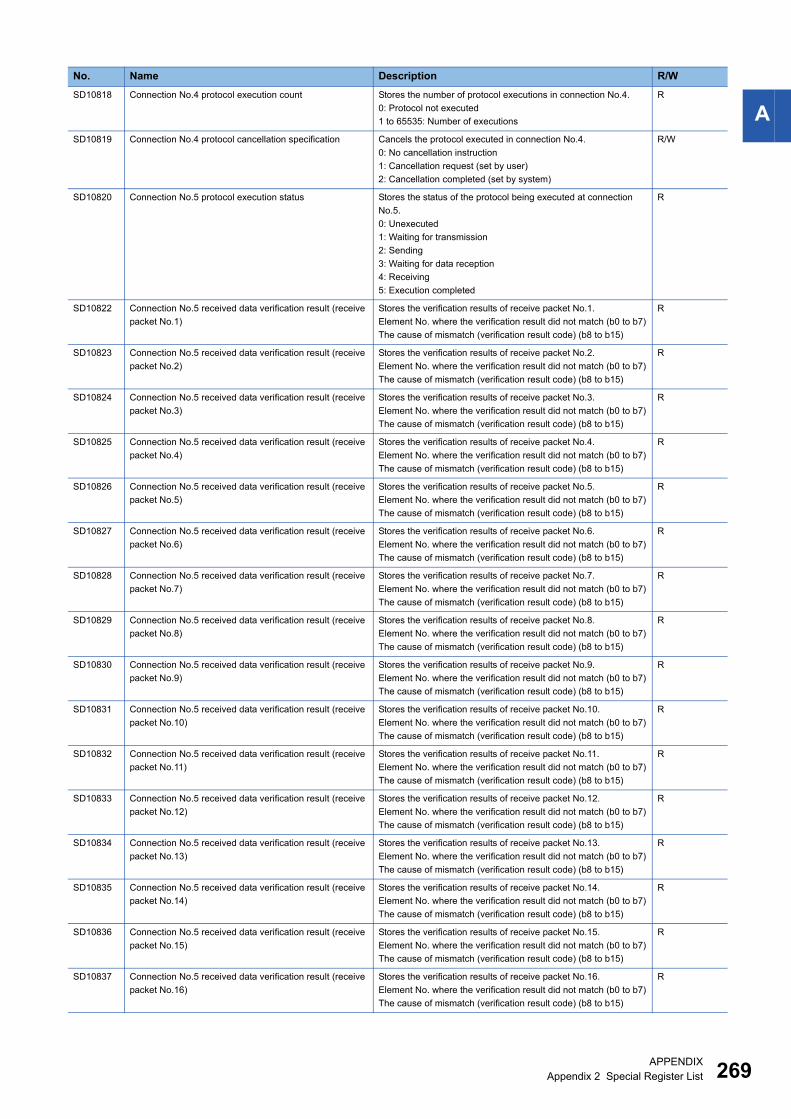
APPENDIX
Appendix 2 Special Register List 269
ASD10818 Connection No.4 protocol execution count Stores the number of protocol executions in connection No.4.
0: Protocol not executed
1 to 65535: Number of executions
R
SD10819 Connection No.4 protocol cancellation specification Cancels the protocol executed in connection No.4.
0: No cancellation instruction
1: Cancellation request (set by user)
2: Cancellation completed (set by system)
R/W
SD10820 Connection No.5 protocol execution status Stores the status of the protocol being executed at connection
No.5.
0: Unexecuted
1: Waiting for transmission
2: Sending
3: Waiting for data reception
4: Receiving
5: Execution completed
R
SD10822 Connection No.5 received data verification result (receive
packet No.1)
Stores the verification results of receive packet No.1.
Element No. where the verification result did not match (b0 to b7)
The cause of mismatch (verification result code) (b8 to b15)
R
SD10823 Connection No.5 received data verification result (receive
packet No.2)
Stores the verification results of receive packet No.2.
Element No. where the verification result did not match (b0 to b7)
The cause of mismatch (verification result code) (b8 to b15)
R
SD10824 Connection No.5 received data verification result (receive
packet No.3)
Stores the verification results of receive packet No.3.
Element No. where the verification result did not match (b0 to b7)
The cause of mismatch (verification result code) (b8 to b15)
R
SD10825 Connection No.5 received data verification result (receive
packet No.4)
Stores the verification results of receive packet No.4.
Element No. where the verification result did not match (b0 to b7)
The cause of mismatch (verification result code) (b8 to b15)
R
SD10826 Connection No.5 received data verification result (receive
packet No.5)
Stores the verification results of receive packet No.5.
Element No. where the verification result did not match (b0 to b7)
The cause of mismatch (verification result code) (b8 to b15)
R
SD10827 Connection No.5 received data verification result (receive
packet No.6)
Stores the verification results of receive packet No.6.
Element No. where the verification result did not match (b0 to b7)
The cause of mismatch (verification result code) (b8 to b15)
R
SD10828 Connection No.5 received data verification result (receive
packet No.7)
Stores the verification results of receive packet No.7.
Element No. where the verification result did not match (b0 to b7)
The cause of mismatch (verification result code) (b8 to b15)
R
SD10829 Connection No.5 received data verification result (receive
packet No.8)
Stores the verification results of receive packet No.8.
Element No. where the verification result did not match (b0 to b7)
The cause of mismatch (verification result code) (b8 to b15)
R
SD10830 Connection No.5 received data verification result (receive
packet No.9)
Stores the verification results of receive packet No.9.
Element No. where the verification result did not match (b0 to b7)
The cause of mismatch (verification result code) (b8 to b15)
R
SD10831 Connection No.5 received data verification result (receive
packet No.10)
Stores the verification results of receive packet No.10.
Element No. where the verification result did not match (b0 to b7)
The cause of mismatch (verification result code) (b8 to b15)
R
SD10832 Connection No.5 received data verification result (receive
packet No.11)
Stores the verification results of receive packet No.11.
Element No. where the verification result did not match (b0 to b7)
The cause of mismatch (verification result code) (b8 to b15)
R
SD10833 Connection No.5 received data verification result (receive
packet No.12)
Stores the verification results of receive packet No.12.
Element No. where the verification result did not match (b0 to b7)
The cause of mismatch (verification result code) (b8 to b15)
R
SD10834 Connection No.5 received data verification result (receive
packet No.13)
Stores the verification results of receive packet No.13.
Element No. where the verification result did not match (b0 to b7)
The cause of mismatch (verification result code) (b8 to b15)
R
SD10835 Connection No.5 received data verification result (receive
packet No.14)
Stores the verification results of receive packet No.14.
Element No. where the verification result did not match (b0 to b7)
The cause of mismatch (verification result code) (b8 to b15)
R
SD10836 Connection No.5 received data verification result (receive
packet No.15)
Stores the verification results of receive packet No.15.
Element No. where the verification result did not match (b0 to b7)
The cause of mismatch (verification result code) (b8 to b15)
R
SD10837 Connection No.5 received data verification result (receive
packet No.16)
Stores the verification results of receive packet No.16.
Element No. where the verification result did not match (b0 to b7)
The cause of mismatch (verification result code) (b8 to b15)
R
No. Name Description R/W

270APPENDIX
Appendix 2 Special Register List
SD10838 Connection No.5 protocol execution count Stores the number of protocol executions in connection No.5.
0: Protocol not executed
1 to 65535: Number of executions
R
SD10839 Connection No.5 protocol cancellation specification Cancels the protocol executed in connection No.5.
0: No cancellation instruction
1: Cancellation request (set by user)
2: Cancellation completed (set by system)
R/W
SD10840 Connection No.6 protocol execution status Stores the status of the protocol being executed at connection
No.6.
0: Unexecuted
1: Waiting for transmission
2: Sending
3: Waiting for data reception
4: Receiving
5: Execution completed
R
SD10842 Connection No.6 received data verification result (receive
packet No.1)
Stores the verification results of receive packet No.1.
Element No. where the verification result did not match (b0 to b7)
The cause of mismatch (verification result code) (b8 to b15)
R
SD10843 Connection No.6 received data verification result (receive
packet No.2)
Stores the verification results of receive packet No.2.
Element No. where the verification result did not match (b0 to b7)
The cause of mismatch (verification result code) (b8 to b15)
R
SD10844 Connection No.6 received data verification result (receive
packet No.3)
Stores the verification results of receive packet No.3.
Element No. where the verification result did not match (b0 to b7)
The cause of mismatch (verification result code) (b8 to b15)
R
SD10845 Connection No.6 received data verification result (receive
packet No.4)
Stores the verification results of receive packet No.4.
Element No. where the verification result did not match (b0 to b7)
The cause of mismatch (verification result code) (b8 to b15)
R
SD10846 Connection No.6 received data verification result (receive
packet No.5)
Stores the verification results of receive packet No.5.
Element No. where the verification result did not match (b0 to b7)
The cause of mismatch (verification result code) (b8 to b15)
R
SD10847 Connection No.6 received data verification result (receive
packet No.6)
Stores the verification results of receive packet No.6.
Element No. where the verification result did not match (b0 to b7)
The cause of mismatch (verification result code) (b8 to b15)
R
SD10848 Connection No.6 received data verification result (receive
packet No.7)
Stores the verification results of receive packet No.7.
Element No. where the verification result did not match (b0 to b7)
The cause of mismatch (verification result code) (b8 to b15)
R
SD10849 Connection No.6 received data verification result (receive
packet No.8)
Stores the verification results of receive packet No.8.
Element No. where the verification result did not match (b0 to b7)
The cause of mismatch (verification result code) (b8 to b15)
R
SD10850 Connection No.6 received data verification result (receive
packet No.9)
Stores the verification results of receive packet No.9.
Element No. where the verification result did not match (b0 to b7)
The cause of mismatch (verification result code) (b8 to b15)
R
SD10851 Connection No.6 received data verification result (receive
packet No.10)
Stores the verification results of receive packet No.10.
Element No. where the verification result did not match (b0 to b7)
The cause of mismatch (verification result code) (b8 to b15)
R
SD10852 Connection No.6 received data verification result (receive
packet No.11)
Stores the verification results of receive packet No.11.
Element No. where the verification result did not match (b0 to b7)
The cause of mismatch (verification result code) (b8 to b15)
R
SD10853 Connection No.6 received data verification result (receive
packet No.12)
Stores the verification results of receive packet No.12.
Element No. where the verification result did not match (b0 to b7)
The cause of mismatch (verification result code) (b8 to b15)
R
SD10854 Connection No.6 received data verification result (receive
packet No.13)
Stores the verification results of receive packet No.13.
Element No. where the verification result did not match (b0 to b7)
The cause of mismatch (verification result code) (b8 to b15)
R
SD10855 Connection No.6 received data verification result (receive
packet No.14)
Stores the verification results of receive packet No.14.
Element No. where the verification result did not match (b0 to b7)
The cause of mismatch (verification result code) (b8 to b15)
R
SD10856 Connection No.6 received data verification result (receive
packet No.15)
Stores the verification results of receive packet No.15.
Element No. where the verification result did not match (b0 to b7)
The cause of mismatch (verification result code) (b8 to b15)
R
SD10857 Connection No.6 received data verification result (receive
packet No.16)
Stores the verification results of receive packet No.16.
Element No. where the verification result did not match (b0 to b7)
The cause of mismatch (verification result code) (b8 to b15)
R
No. Name Description R/W
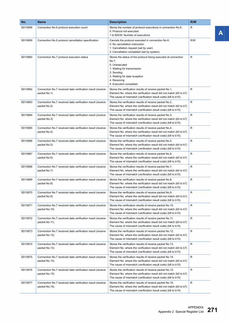
APPENDIX
Appendix 2 Special Register List 271
ASD10858 Connection No.6 protocol execution count Stores the number of protocol executions in connection No.6.
0: Protocol not executed
1 to 65535: Number of executions
R
SD10859 Connection No.6 protocol cancellation specification Cancels the protocol executed in connection No.6.
0: No cancellation instruction
1: Cancellation request (set by user)
2: Cancellation completed (set by system)
R/W
SD10860 Connection No.7 protocol execution status Stores the status of the protocol being executed at connection
No.7.
0: Unexecuted
1: Waiting for transmission
2: Sending
3: Waiting for data reception
4: Receiving
5: Execution completed
R
SD10862 Connection No.7 received data verification result (receive
packet No.1)
Stores the verification results of receive packet No.1.
Element No. where the verification result did not match (b0 to b7)
The cause of mismatch (verification result code) (b8 to b15)
R
SD10863 Connection No.7 received data verification result (receive
packet No.2)
Stores the verification results of receive packet No.2.
Element No. where the verification result did not match (b0 to b7)
The cause of mismatch (verification result code) (b8 to b15)
R
SD10864 Connection No.7 received data verification result (receive
packet No.3)
Stores the verification results of receive packet No.3.
Element No. where the verification result did not match (b0 to b7)
The cause of mismatch (verification result code) (b8 to b15)
R
SD10865 Connection No.7 received data verification result (receive
packet No.4)
Stores the verification results of receive packet No.4.
Element No. where the verification result did not match (b0 to b7)
The cause of mismatch (verification result code) (b8 to b15)
R
SD10866 Connection No.7 received data verification result (receive
packet No.5)
Stores the verification results of receive packet No.5.
Element No. where the verification result did not match (b0 to b7)
The cause of mismatch (verification result code) (b8 to b15)
R
SD10867 Connection No.7 received data verification result (receive
packet No.6)
Stores the verification results of receive packet No.6.
Element No. where the verification result did not match (b0 to b7)
The cause of mismatch (verification result code) (b8 to b15)
R
SD10868 Connection No.7 received data verification result (receive
packet No.7)
Stores the verification results of receive packet No.7.
Element No. where the verification result did not match (b0 to b7)
The cause of mismatch (verification result code) (b8 to b15)
R
SD10869 Connection No.7 received data verification result (receive
packet No.8)
Stores the verification results of receive packet No.8.
Element No. where the verification result did not match (b0 to b7)
The cause of mismatch (verification result code) (b8 to b15)
R
SD10870 Connection No.7 received data verification result (receive
packet No.9)
Stores the verification results of receive packet No.9.
Element No. where the verification result did not match (b0 to b7)
The cause of mismatch (verification result code) (b8 to b15)
R
SD10871 Connection No.7 received data verification result (receive
packet No.10)
Stores the verification results of receive packet No.10.
Element No. where the verification result did not match (b0 to b7)
The cause of mismatch (verification result code) (b8 to b15)
R
SD10872 Connection No.7 received data verification result (receive
packet No.11)
Stores the verification results of receive packet No.11.
Element No. where the verification result did not match (b0 to b7)
The cause of mismatch (verification result code) (b8 to b15)
R
SD10873 Connection No.7 received data verification result (receive
packet No.12)
Stores the verification results of receive packet No.12.
Element No. where the verification result did not match (b0 to b7)
The cause of mismatch (verification result code) (b8 to b15)
R
SD10874 Connection No.7 received data verification result (receive
packet No.13)
Stores the verification results of receive packet No.13.
Element No. where the verification result did not match (b0 to b7)
The cause of mismatch (verification result code) (b8 to b15)
R
SD10875 Connection No.7 received data verification result (receive
packet No.14)
Stores the verification results of receive packet No.14.
Element No. where the verification result did not match (b0 to b7)
The cause of mismatch (verification result code) (b8 to b15)
R
SD10876 Connection No.7 received data verification result (receive
packet No.15)
Stores the verification results of receive packet No.15.
Element No. where the verification result did not match (b0 to b7)
The cause of mismatch (verification result code) (b8 to b15)
R
SD10877 Connection No.7 received data verification result (receive
packet No.16)
Stores the verification results of receive packet No.16.
Element No. where the verification result did not match (b0 to b7)
The cause of mismatch (verification result code) (b8 to b15)
R
No. Name Description R/W
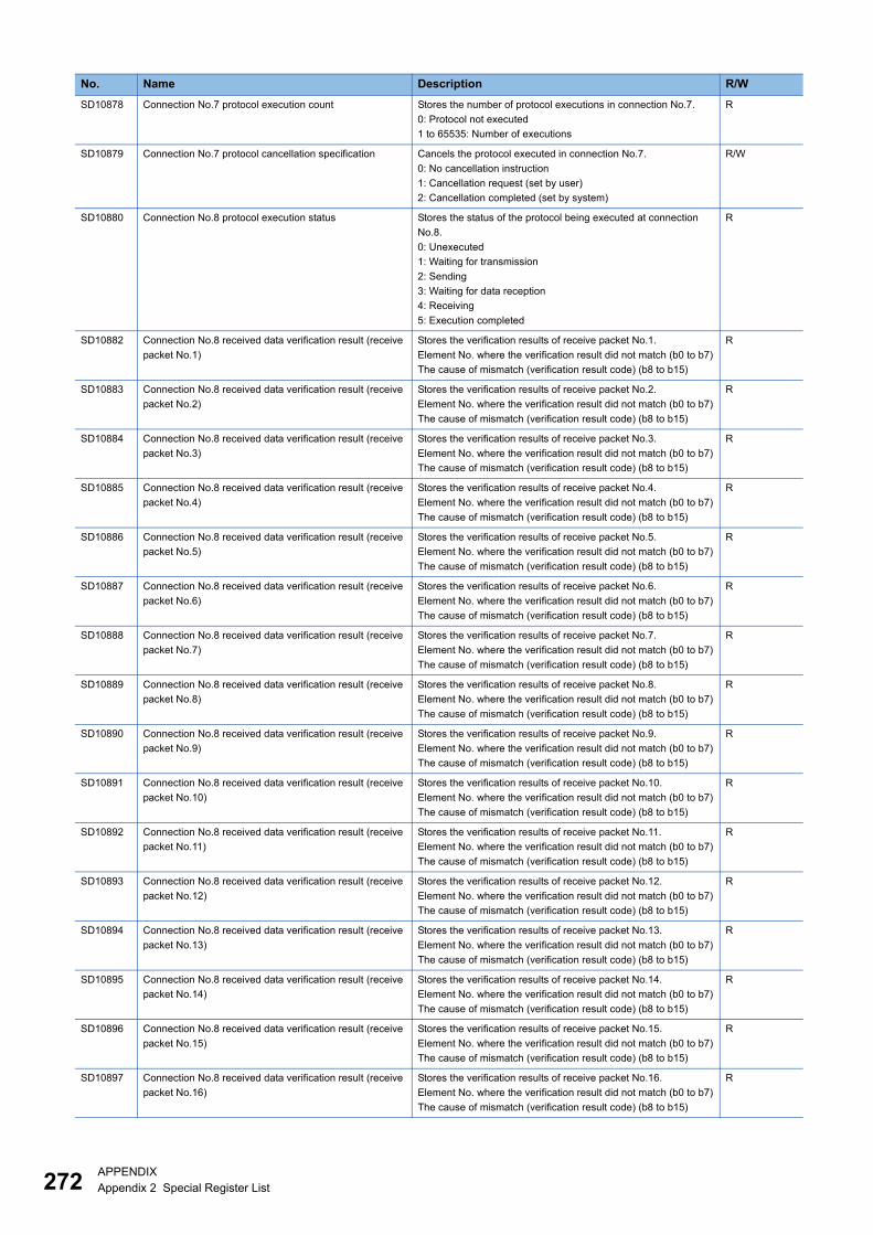
272APPENDIX
Appendix 2 Special Register List
SD10878 Connection No.7 protocol execution count Stores the number of protocol executions in connection No.7.
0: Protocol not executed
1 to 65535: Number of executions
R
SD10879 Connection No.7 protocol cancellation specification Cancels the protocol executed in connection No.7.
0: No cancellation instruction
1: Cancellation request (set by user)
2: Cancellation completed (set by system)
R/W
SD10880 Connection No.8 protocol execution status Stores the status of the protocol being executed at connection
No.8.
0: Unexecuted
1: Waiting for transmission
2: Sending
3: Waiting for data reception
4: Receiving
5: Execution completed
R
SD10882 Connection No.8 received data verification result (receive
packet No.1)
Stores the verification results of receive packet No.1.
Element No. where the verification result did not match (b0 to b7)
The cause of mismatch (verification result code) (b8 to b15)
R
SD10883 Connection No.8 received data verification result (receive
packet No.2)
Stores the verification results of receive packet No.2.
Element No. where the verification result did not match (b0 to b7)
The cause of mismatch (verification result code) (b8 to b15)
R
SD10884 Connection No.8 received data verification result (receive
packet No.3)
Stores the verification results of receive packet No.3.
Element No. where the verification result did not match (b0 to b7)
The cause of mismatch (verification result code) (b8 to b15)
R
SD10885 Connection No.8 received data verification result (receive
packet No.4)
Stores the verification results of receive packet No.4.
Element No. where the verification result did not match (b0 to b7)
The cause of mismatch (verification result code) (b8 to b15)
R
SD10886 Connection No.8 received data verification result (receive
packet No.5)
Stores the verification results of receive packet No.5.
Element No. where the verification result did not match (b0 to b7)
The cause of mismatch (verification result code) (b8 to b15)
R
SD10887 Connection No.8 received data verification result (receive
packet No.6)
Stores the verification results of receive packet No.6.
Element No. where the verification result did not match (b0 to b7)
The cause of mismatch (verification result code) (b8 to b15)
R
SD10888 Connection No.8 received data verification result (receive
packet No.7)
Stores the verification results of receive packet No.7.
Element No. where the verification result did not match (b0 to b7)
The cause of mismatch (verification result code) (b8 to b15)
R
SD10889 Connection No.8 received data verification result (receive
packet No.8)
Stores the verification results of receive packet No.8.
Element No. where the verification result did not match (b0 to b7)
The cause of mismatch (verification result code) (b8 to b15)
R
SD10890 Connection No.8 received data verification result (receive
packet No.9)
Stores the verification results of receive packet No.9.
Element No. where the verification result did not match (b0 to b7)
The cause of mismatch (verification result code) (b8 to b15)
R
SD10891 Connection No.8 received data verification result (receive
packet No.10)
Stores the verification results of receive packet No.10.
Element No. where the verification result did not match (b0 to b7)
The cause of mismatch (verification result code) (b8 to b15)
R
SD10892 Connection No.8 received data verification result (receive
packet No.11)
Stores the verification results of receive packet No.11.
Element No. where the verification result did not match (b0 to b7)
The cause of mismatch (verification result code) (b8 to b15)
R
SD10893 Connection No.8 received data verification result (receive
packet No.12)
Stores the verification results of receive packet No.12.
Element No. where the verification result did not match (b0 to b7)
The cause of mismatch (verification result code) (b8 to b15)
R
SD10894 Connection No.8 received data verification result (receive
packet No.13)
Stores the verification results of receive packet No.13.
Element No. where the verification result did not match (b0 to b7)
The cause of mismatch (verification result code) (b8 to b15)
R
SD10895 Connection No.8 received data verification result (receive
packet No.14)
Stores the verification results of receive packet No.14.
Element No. where the verification result did not match (b0 to b7)
The cause of mismatch (verification result code) (b8 to b15)
R
SD10896 Connection No.8 received data verification result (receive
packet No.15)
Stores the verification results of receive packet No.15.
Element No. where the verification result did not match (b0 to b7)
The cause of mismatch (verification result code) (b8 to b15)
R
SD10897 Connection No.8 received data verification result (receive
packet No.16)
Stores the verification results of receive packet No.16.
Element No. where the verification result did not match (b0 to b7)
The cause of mismatch (verification result code) (b8 to b15)
R
No. Name Description R/W
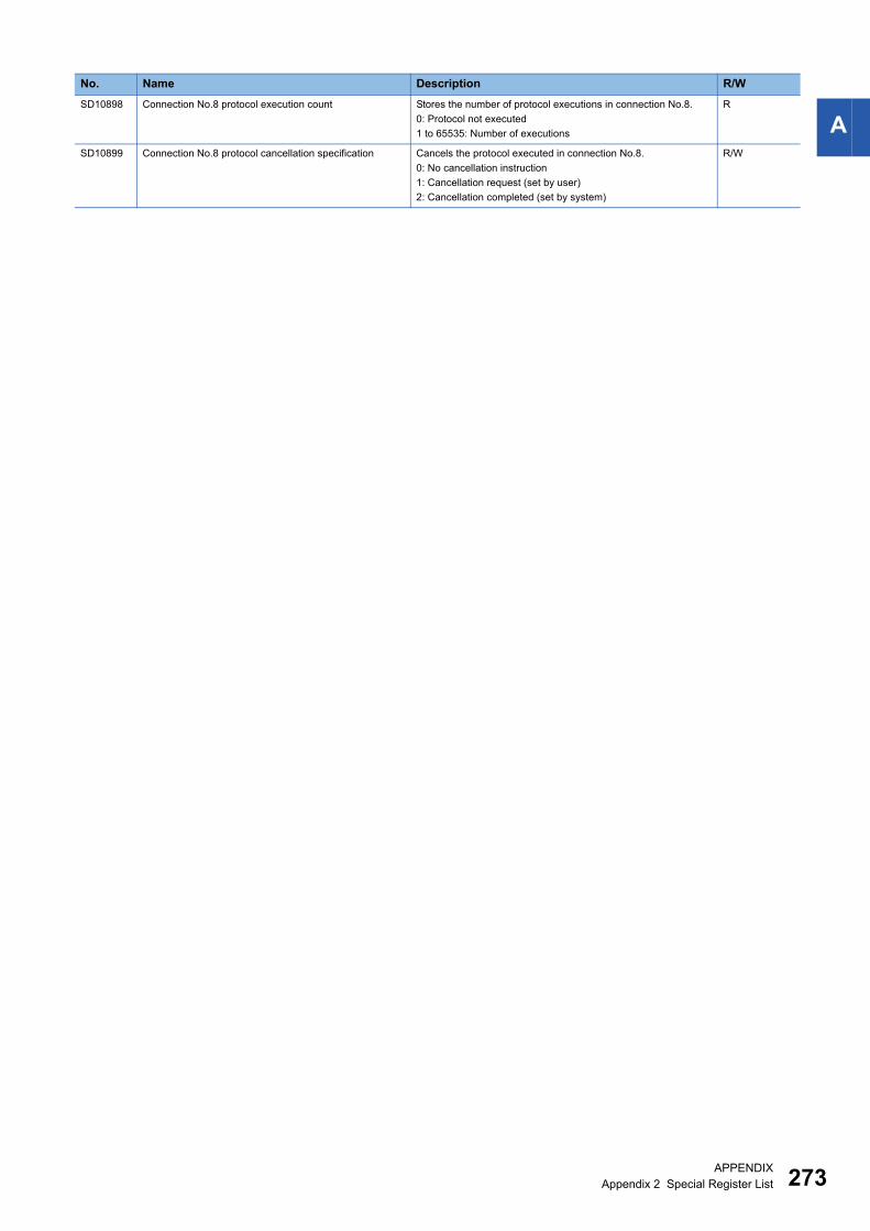
APPENDIX
Appendix 2 Special Register List 273
ASD10898 Connection No.8 protocol execution count Stores the number of protocol executions in connection No.8.
0: Protocol not executed
1 to 65535: Number of executions
R
SD10899 Connection No.8 protocol cancellation specification Cancels the protocol executed in connection No.8.
0: No cancellation instruction
1: Cancellation request (set by user)
2: Cancellation completed (set by system)
R/W
No. Name Description R/W
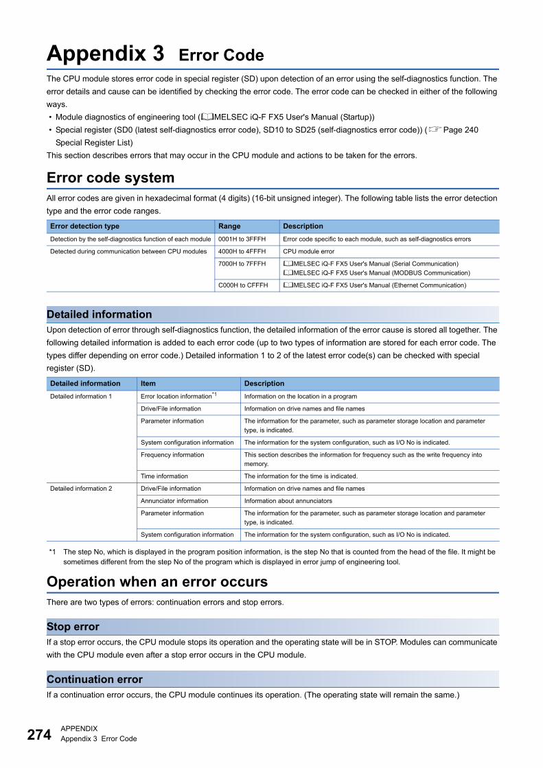
274APPENDIX
Appendix 3 Error Code
Appendix 3 Error Code
The CPU module stores error code in special register (SD) upon detection of an error using the self-diagnostics function. The
error details and cause can be identified by checking the error code. The error code can be checked in either of the following
ways.
� Module diagnostics of engineering tool (MELSEC iQ-F FX5 User's Manual (Startup))
� Special register (SD0 (latest self-diagnostics error code), SD10 to SD25 (self-diagnostics error code)) (Page 240
Special Register List)
This section describes errors that may occur in the CPU module and actions to be taken for the errors.
Error code system
All error codes are given in hexadecimal format (4 digits) (16-bit unsigned integer). The following table lists the error detection
type and the error code ranges.
Detailed information
Upon detection of error through self-diagnostics function, the detailed information of the error cause is stored all together. The
following detailed information is added to each error code (up to two types of information are stored for each error code. The
types differ depending on error code.) Detailed information 1 to 2 of the latest error code(s) can be checked with special
register (SD).
*1 The step No, which is displayed in the program position information, is the step No that is counted from the head of the file. It might be
sometimes different from the step No of the program which is displayed in error jump of engineering tool.
Operation when an error occurs
There are two types of errors: continuation errors and stop errors.
Stop error
If a stop error occurs, the CPU module stops its operation and the operating state will be in STOP. Modules can communicate
with the CPU module even after a stop error occurs in the CPU module.
Continuation error
If a continuation error occurs, the CPU module continues its operation. (The operating state will remain the same.)
Error detection type Range Description
Detection by the self-diagnostics function of each module 0001H to 3FFFH Error code specific to each module, such as self-diagnostics errors
Detected during communication between CPU modules 4000H to 4FFFH CPU module error
7000H to 7FFFH MELSEC iQ-F FX5 User's Manual (Serial Communication)
MELSEC iQ-F FX5 User's Manual (MODBUS Communication)
C000H to CFFFH MELSEC iQ-F FX5 User's Manual (Ethernet Communication)
Detailed information Item Description
Detailed information 1 Error location information*1 Information on the location in a program
Drive/File information Information on drive names and file names
Parameter information The information for the parameter, such as parameter storage location and parameter
type, is indicated.
System configuration information The information for the system configuration, such as I/O No is indicated.
Frequency information This section describes the information for frequency such as the write frequency into
memory.
Time information The information for the time is indicated.
Detailed information 2 Drive/File information Information on drive names and file names
Annunciator information Information about annunciators
Parameter information The information for the parameter, such as parameter storage location and parameter
type, is indicated.
System configuration information The information for the system configuration, such as I/O No is indicated.
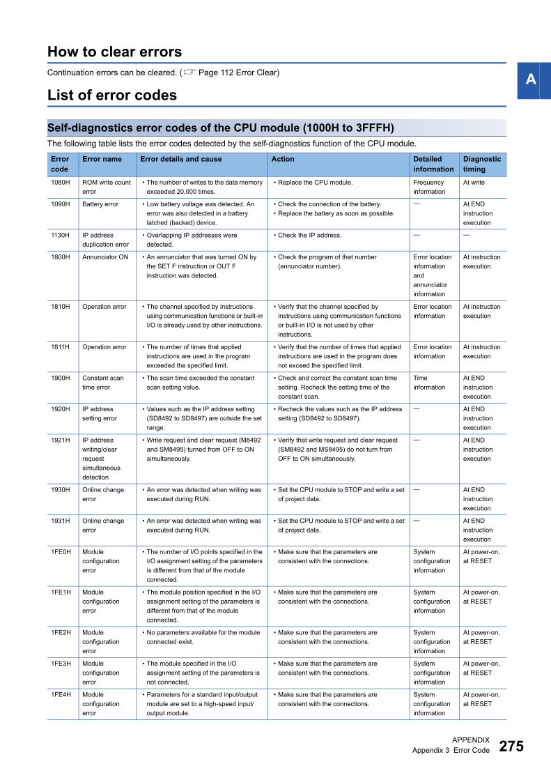
APPENDIX
Appendix 3 Error Code 275
A
How to clear errors
Continuation errors can be cleared. (Page 112 Error Clear)
List of error codes
Self-diagnostics error codes of the CPU module (1000H to 3FFFH)
The following table lists the error codes detected by the self-diagnostics function of the CPU module.
Error
code
Error name Error details and cause Action Detailed
information
Diagnostic
timing
1080H ROM write count
error
� The number of writes to the data memory
exceeded 20,000 times.
� Replace the CPU module. Frequency
information
At write
1090H Battery error � Low battery voltage was detected. An
error was also detected in a battery
latched (backed) device.
� Check the connection of the battery.
� Replace the battery as soon as possible.
At END
instruction
execution
1130H IP address
duplication error
� Overlapping IP addresses were
detected.
� Check the IP address.
1800H Annunciator ON � An annunciator that was turned ON by
the SET F instruction or OUT F
instruction was detected.
� Check the program of that number
(annunciator number).
Error location
information
and
annunciator
information
At instruction
execution
1810H Operation error � The channel specified by instructions
using communication functions or built-in
I/O is already used by other instructions.
� Verify that the channel specified by
instructions using communication functions
or built-in I/O is not used by other
instructions.
Error location
information
At instruction
execution
1811H Operation error � The number of times that applied
instructions are used in the program
exceeded the specified limit.
� Verify that the number of times that applied
instructions are used in the program does
not exceed the specified limit.
Error location
information
At instruction
execution
1900H Constant scan
time error
� The scan time exceeded the constant
scan setting value.
� Check and correct the constant scan time
setting. Recheck the setting time of the
constant scan.
Time
information
At END
instruction
execution
1920H IP address
setting error
� Values such as the IP address setting
(SD8492 to SD8497) are outside the set
range.
� Recheck the values such as the IP address
setting (SD8492 to SD8497).
At END
instruction
execution
1921H IP address
writing/clear
request
simultaneous
detection
� Write request and clear request (M8492
and SM8495) turned from OFF to ON
simultaneously.
� Verify that write request and clear request
(SM8492 and MS8495) do not turn from
OFF to ON simultaneously.
At END
instruction
execution
1930H Online change
error
� An error was detected when writing was
executed during RUN.
� Set the CPU module to STOP and write a set
of project data.
At END
instruction
execution
1931H Online change
error
� An error was detected when writing was
executed during RUN.
� Set the CPU module to STOP and write a set
of project data.
At END
instruction
execution
1FE0H Module
configuration
error
� The number of I/O points specified in the
I/O assignment setting of the parameters
is different from that of the module
connected.
� Make sure that the parameters are
consistent with the connections.
System
configuration
information
At power-on,
at RESET
1FE1H Module
configuration
error
� The module position specified in the I/O
assignment setting of the parameters is
different from that of the module
connected.
� Make sure that the parameters are
consistent with the connections.
System
configuration
information
At power-on,
at RESET
1FE2H Module
configuration
error
� No parameters available for the module
connected exist.
� Make sure that the parameters are
consistent with the connections.
System
configuration
information
At power-on,
at RESET
1FE3H Module
configuration
error
� The module specified in the I/O
assignment setting of the parameters is
not connected.
� Make sure that the parameters are
consistent with the connections.
System
configuration
information
At power-on,
at RESET
1FE4H Module
configuration
error
� Parameters for a standard input/output
module are set to a high-speed input/
output module.
� Make sure that the parameters are
consistent with the connections.
System
configuration
information
At power-on,
at RESET
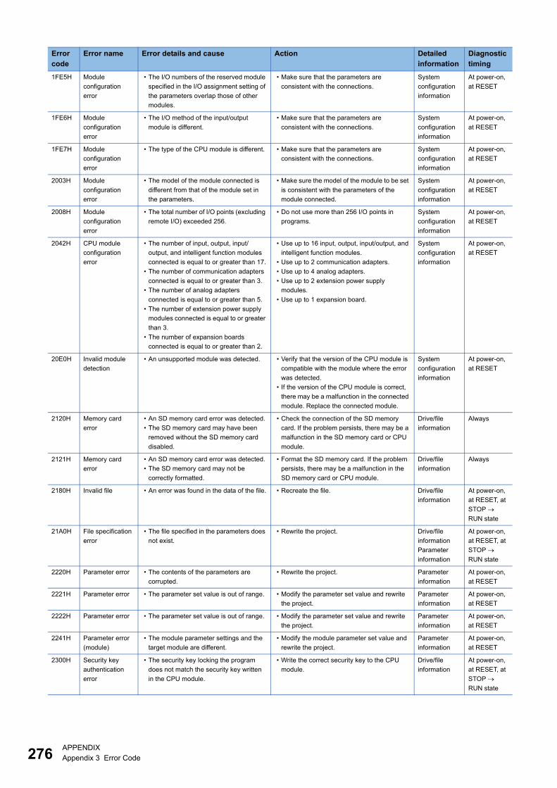
276APPENDIX
Appendix 3 Error Code
1FE5H Module
configuration
error
� The I/O numbers of the reserved module
specified in the I/O assignment setting of
the parameters overlap those of other
modules.
� Make sure that the parameters are
consistent with the connections.
System
configuration
information
At power-on,
at RESET
1FE6H Module
configuration
error
� The I/O method of the input/output
module is different.
� Make sure that the parameters are
consistent with the connections.
System
configuration
information
At power-on,
at RESET
1FE7H Module
configuration
error
� The type of the CPU module is different. � Make sure that the parameters are
consistent with the connections.
System
configuration
information
At power-on,
at RESET
2003H Module
configuration
error
� The model of the module connected is
different from that of the module set in
the parameters.
� Make sure the model of the module to be set
is consistent with the parameters of the
module connected.
System
configuration
information
At power-on,
at RESET
2008H Module
configuration
error
� The total number of I/O points (excluding
remote I/O) exceeded 256.
� Do not use more than 256 I/O points in
programs.
System
configuration
information
At power-on,
at RESET
2042H CPU module
configuration
error
� The number of input, output, input/
output, and intelligent function modules
connected is equal to or greater than 17.
� The number of communication adapters
connected is equal to or greater than 3.
� The number of analog adapters
connected is equal to or greater than 5.
� The number of extension power supply
modules connected is equal to or greater
than 3.
� The number of expansion boards
connected is equal to or greater than 2.
� Use up to 16 input, output, input/output, and
intelligent function modules.
� Use up to 2 communication adapters.
� Use up to 4 analog adapters.
� Use up to 2 extension power supply
modules.
� Use up to 1 expansion board.
System
configuration
information
At power-on,
at RESET
20E0H Invalid module
detection
� An unsupported module was detected. � Verify that the version of the CPU module is
compatible with the module where the error
was detected.
� If the version of the CPU module is correct,
there may be a malfunction in the connected
module. Replace the connected module.
System
configuration
information
At power-on,
at RESET
2120H Memory card
error
� An SD memory card error was detected.
� The SD memory card may have been
removed without the SD memory card
disabled.
� Check the connection of the SD memory
card. If the problem persists, there may be a
malfunction in the SD memory card or CPU
module.
Drive/file
information
Always
2121H Memory card
error
� An SD memory card error was detected.
� The SD memory card may not be
correctly formatted.
� Format the SD memory card. If the problem
persists, there may be a malfunction in the
SD memory card or CPU module.
Drive/file
information
Always
2180H Invalid file � An error was found in the data of the file. � Recreate the file. Drive/file
information
At power-on,
at RESET, at
STOP
RUN state
21A0H File specification
error
� The file specified in the parameters does
not exist.
� Rewrite the project. Drive/file
information
Parameter
information
At power-on,
at RESET, at
STOP
RUN state
2220H Parameter error � The contents of the parameters are
corrupted.
� Rewrite the project. Parameter
information
At power-on,
at RESET
2221H Parameter error � The parameter set value is out of range. � Modify the parameter set value and rewrite
the project.
Parameter
information
At power-on,
at RESET
2222H Parameter error � The parameter set value is out of range. � Modify the parameter set value and rewrite
the project.
Parameter
information
At power-on,
at RESET
2241H Parameter error
(module)
� The module parameter settings and the
target module are different.
� Modify the module parameter set value and
rewrite the project.
Parameter
information
At power-on,
at RESET
2300H Security key
authentication
error
� The security key locking the program
does not match the security key written
in the CPU module.
� Write the correct security key to the CPU
module.
Drive/file
information
At power-on,
at RESET, at
STOP
RUN state
Error
code
Error name Error details and cause Action Detailed
information
Diagnostic
timing
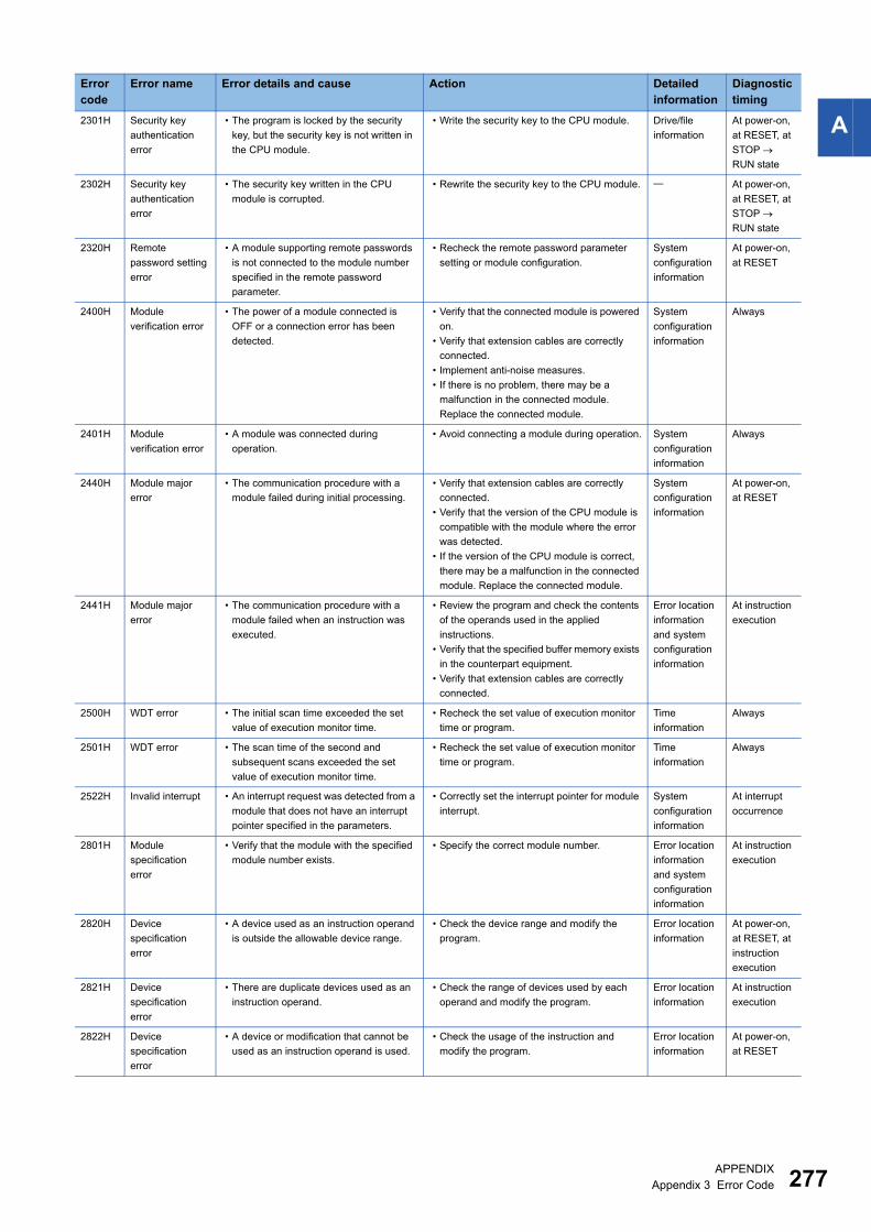
APPENDIX
Appendix 3 Error Code 277
A2301H Security key
authentication
error
� The program is locked by the security
key, but the security key is not written in
the CPU module.
� Write the security key to the CPU module. Drive/file
information
At power-on,
at RESET, at
STOP
RUN state
2302H Security key
authentication
error
� The security key written in the CPU
module is corrupted.
� Rewrite the security key to the CPU module. At power-on,
at RESET, at
STOP
RUN state
2320H Remote
password setting
error
� A module supporting remote passwords
is not connected to the module number
specified in the remote password
parameter.
� Recheck the remote password parameter
setting or module configuration.
System
configuration
information
At power-on,
at RESET
2400H Module
verification error
� The power of a module connected is
OFF or a connection error has been
detected.
� Verify that the connected module is powered
on.
� Verify that extension cables are correctly
connected.
� Implement anti-noise measures.
� If there is no problem, there may be a
malfunction in the connected module.
Replace the connected module.
System
configuration
information
Always
2401H Module
verification error
� A module was connected during
operation.
� Avoid connecting a module during operation. System
configuration
information
Always
2440H Module major
error
� The communication procedure with a
module failed during initial processing.
� Verify that extension cables are correctly
connected.
� Verify that the version of the CPU module is
compatible with the module where the error
was detected.
� If the version of the CPU module is correct,
there may be a malfunction in the connected
module. Replace the connected module.
System
configuration
information
At power-on,
at RESET
2441H Module major
error
� The communication procedure with a
module failed when an instruction was
executed.
� Review the program and check the contents
of the operands used in the applied
instructions.
� Verify that the specified buffer memory exists
in the counterpart equipment.
� Verify that extension cables are correctly
connected.
Error location
information
and system
configuration
information
At instruction
execution
2500H WDT error � The initial scan time exceeded the set
value of execution monitor time.
� Recheck the set value of execution monitor
time or program.
Time
information
Always
2501H WDT error � The scan time of the second and
subsequent scans exceeded the set
value of execution monitor time.
� Recheck the set value of execution monitor
time or program.
Time
information
Always
2522H Invalid interrupt � An interrupt request was detected from a
module that does not have an interrupt
pointer specified in the parameters.
� Correctly set the interrupt pointer for module
interrupt.
System
configuration
information
At interrupt
occurrence
2801H Module
specification
error
� Verify that the module with the specified
module number exists.
� Specify the correct module number. Error location
information
and system
configuration
information
At instruction
execution
2820H Device
specification
error
� A device used as an instruction operand
is outside the allowable device range.
� Check the device range and modify the
program.
Error location
information
At power-on,
at RESET, at
instruction
execution
2821H Device
specification
error
� There are duplicate devices used as an
instruction operand.
� Check the range of devices used by each
operand and modify the program.
Error location
information
At instruction
execution
2822H Device
specification
error
� A device or modification that cannot be
used as an instruction operand is used.
� Check the usage of the instruction and
modify the program.
Error location
information
At power-on,
at RESET
Error
code
Error name Error details and cause Action Detailed
information
Diagnostic
timing
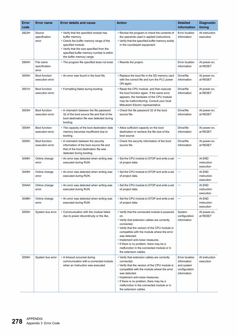
278APPENDIX
Appendix 3 Error Code
2823H Device
specification
error
� Verify that the specified module has
buffer memory.
� Check the buffer memory range of the
specified module.
� Verify that the size specified from the
specified buffer memory number is within
the buffer memory range.
� Review the program or check the contents of
the operands used in applied instructions.
� Verify that the specified buffer memory exists
in the counterpart equipment.
Error location
information
At instruction
execution
2840H File name
specification
error
� The program file specified does not exist. � Rewrite the project. Error location
information
At power-on,
at RESET
3000H Boot function
execution error
� An error was found in the boot file. � Replace the boot file in the SD memory card
with the correct file and turn the PLC power
ON again.
Drive/file
information
At power-on,
at RESET
3001H Boot function
execution error
� Formatting failed during booting. � Reset the CPU module, and then execute
the boot function again. If the same error
appears, the hardware of the CPU module
may be malfunctioning. Consult your local
Mitsubishi Electric representative.
Drive/file
information
At power-on,
at RESET
3003H Boot function
execution error
� A mismatch between the file password
32 of the boot source file and that of the
boot destination file was detected during
booting.
� Check the file password 32 of the boot
source file.
Drive/file
information
At power-on,
at RESET
3004H Boot function
execution error
� The capacity of the boot destination data
memory becomes insufficient due to
booting.
� Allow sufficient capacity on the boot
destination or recheck the file size of the
boot source.
Drive/file
information
At power-on,
at RESET
3005H Boot function
execution error
� A mismatch between the security
information of the boot source file and
that of the boot destination file was
detected during booting.
� Check the security information of the boot
source file.
Drive/file
information
At power-on,
at RESET
3048H Online change
error
� An error was detected when writing was
executed during RUN.
� Set the CPU module to STOP and write a set
of project data.
At END
instruction
execution
3049H Online change
error
� An error was detected when writing was
executed during RUN.
� Set the CPU module to STOP and write a set
of project data.
At END
instruction
execution
304AH Online change
error
� An error was detected when writing was
executed during RUN.
� Set the CPU module to STOP and write a set
of project data.
At END
instruction
execution
304BH Online change
error
� An error was detected when writing was
executed during RUN.
� Set the CPU module to STOP and write a set
of project data.
At END
instruction
execution
3050H System bus error � Communication with the module failed
due to power discontinuity or the like.
� Verify that the connected module is powered
on.
� Verify that extension cables are correctly
connected.
� Verify that the version of the CPU module is
compatible with the module where the error
was detected.
� Implement anti-noise measures.
� If there is no problem, there may be a
malfunction in the connected module or in
the extension cables.
System
configuration
information
At power-on,
at RESET
3056H System bus error � A timeout occurred during
communication with a connected module
when an instruction was executed.
� Verify that extension cables are correctly
connected.
� Verify that the version of the CPU module is
compatible with the module where the error
was detected.
� Implement anti-noise measures.
� If there is no problem, there may be a
malfunction in the connected module or in
the extension cables.
Error location
information
and system
configuration
information
At instruction
execution
Error
code
Error name Error details and cause Action Detailed
information
Diagnostic
timing
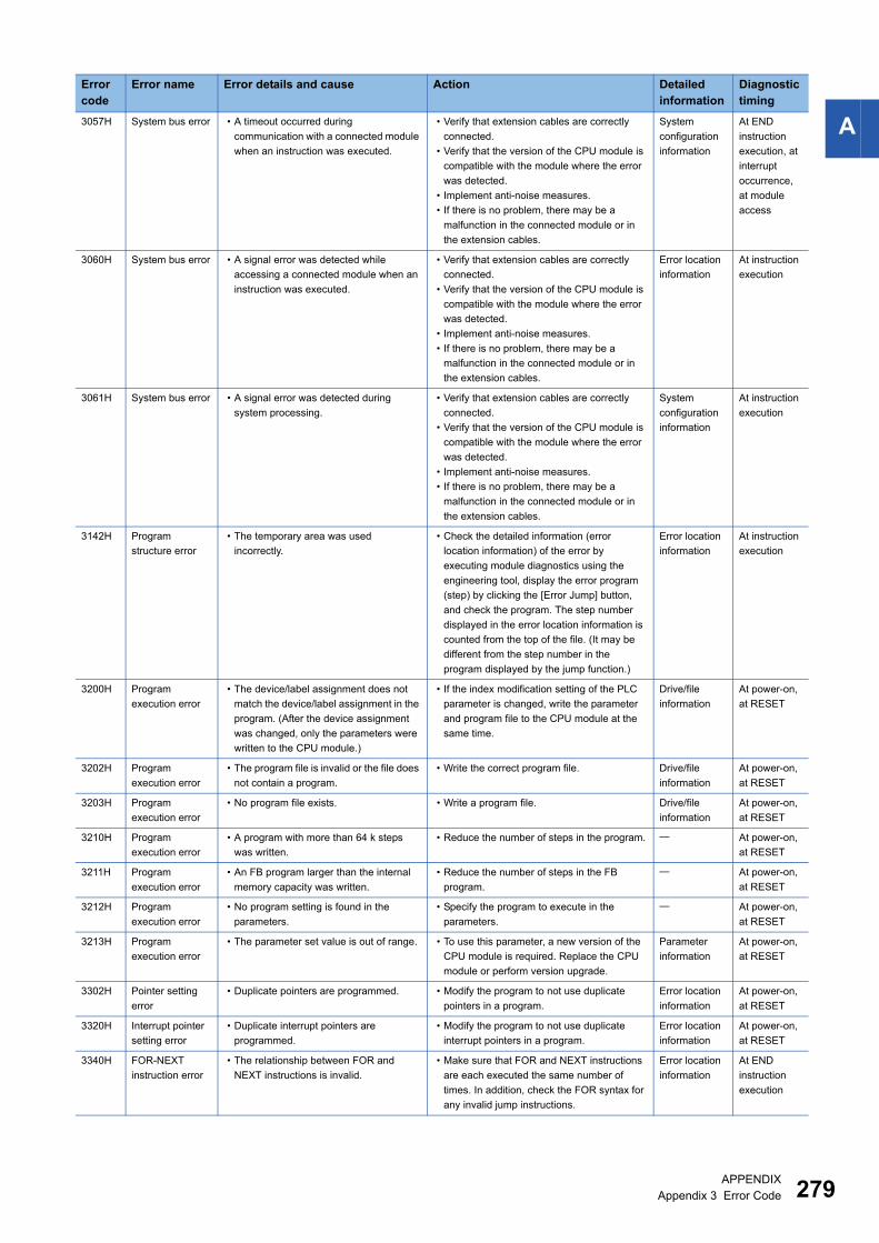
APPENDIX
Appendix 3 Error Code 279
A3057H System bus error � A timeout occurred during
communication with a connected module
when an instruction was executed.
� Verify that extension cables are correctly
connected.
� Verify that the version of the CPU module is
compatible with the module where the error
was detected.
� Implement anti-noise measures.
� If there is no problem, there may be a
malfunction in the connected module or in
the extension cables.
System
configuration
information
At END
instruction
execution, at
interrupt
occurrence,
at module
access
3060H System bus error � A signal error was detected while
accessing a connected module when an
instruction was executed.
� Verify that extension cables are correctly
connected.
� Verify that the version of the CPU module is
compatible with the module where the error
was detected.
� Implement anti-noise measures.
� If there is no problem, there may be a
malfunction in the connected module or in
the extension cables.
Error location
information
At instruction
execution
3061H System bus error � A signal error was detected during
system processing.
� Verify that extension cables are correctly
connected.
� Verify that the version of the CPU module is
compatible with the module where the error
was detected.
� Implement anti-noise measures.
� If there is no problem, there may be a
malfunction in the connected module or in
the extension cables.
System
configuration
information
At instruction
execution
3142H Program
structure error
� The temporary area was used
incorrectly.
� Check the detailed information (error
location information) of the error by
executing module diagnostics using the
engineering tool, display the error program
(step) by clicking the [Error Jump] button,
and check the program. The step number
displayed in the error location information is
counted from the top of the file. (It may be
different from the step number in the
program displayed by the jump function.)
Error location
information
At instruction
execution
3200H Program
execution error
� The device/label assignment does not
match the device/label assignment in the
program. (After the device assignment
was changed, only the parameters were
written to the CPU module.)
� If the index modification setting of the PLC
parameter is changed, write the parameter
and program file to the CPU module at the
same time.
Drive/file
information
At power-on,
at RESET
3202H Program
execution error
� The program file is invalid or the file does
not contain a program.
� Write the correct program file. Drive/file
information
At power-on,
at RESET
3203H Program
execution error
� No program file exists. � Write a program file. Drive/file
information
At power-on,
at RESET
3210H Program
execution error
� A program with more than 64 k steps
was written.
� Reduce the number of steps in the program. At power-on,
at RESET
3211H Program
execution error
� An FB program larger than the internal
memory capacity was written.
� Reduce the number of steps in the FB
program.
At power-on,
at RESET
3212H Program
execution error
� No program setting is found in the
parameters.
� Specify the program to execute in the
parameters.
At power-on,
at RESET
3213H Program
execution error
� The parameter set value is out of range. � To use this parameter, a new version of the
CPU module is required. Replace the CPU
module or perform version upgrade.
Parameter
information
At power-on,
at RESET
3302H Pointer setting
error
� Duplicate pointers are programmed. � Modify the program to not use duplicate
pointers in a program.
Error location
information
At power-on,
at RESET
3320H Interrupt pointer
setting error
� Duplicate interrupt pointers are
programmed.
� Modify the program to not use duplicate
interrupt pointers in a program.
Error location
information
At power-on,
at RESET
3340H FOR-NEXT
instruction error
� The relationship between FOR and
NEXT instructions is invalid.
� Make sure that FOR and NEXT instructions
are each executed the same number of
times. In addition, check the FOR syntax for
any invalid jump instructions.
Error location
information
At END
instruction
execution
Error
code
Error name Error details and cause Action Detailed
information
Diagnostic
timing
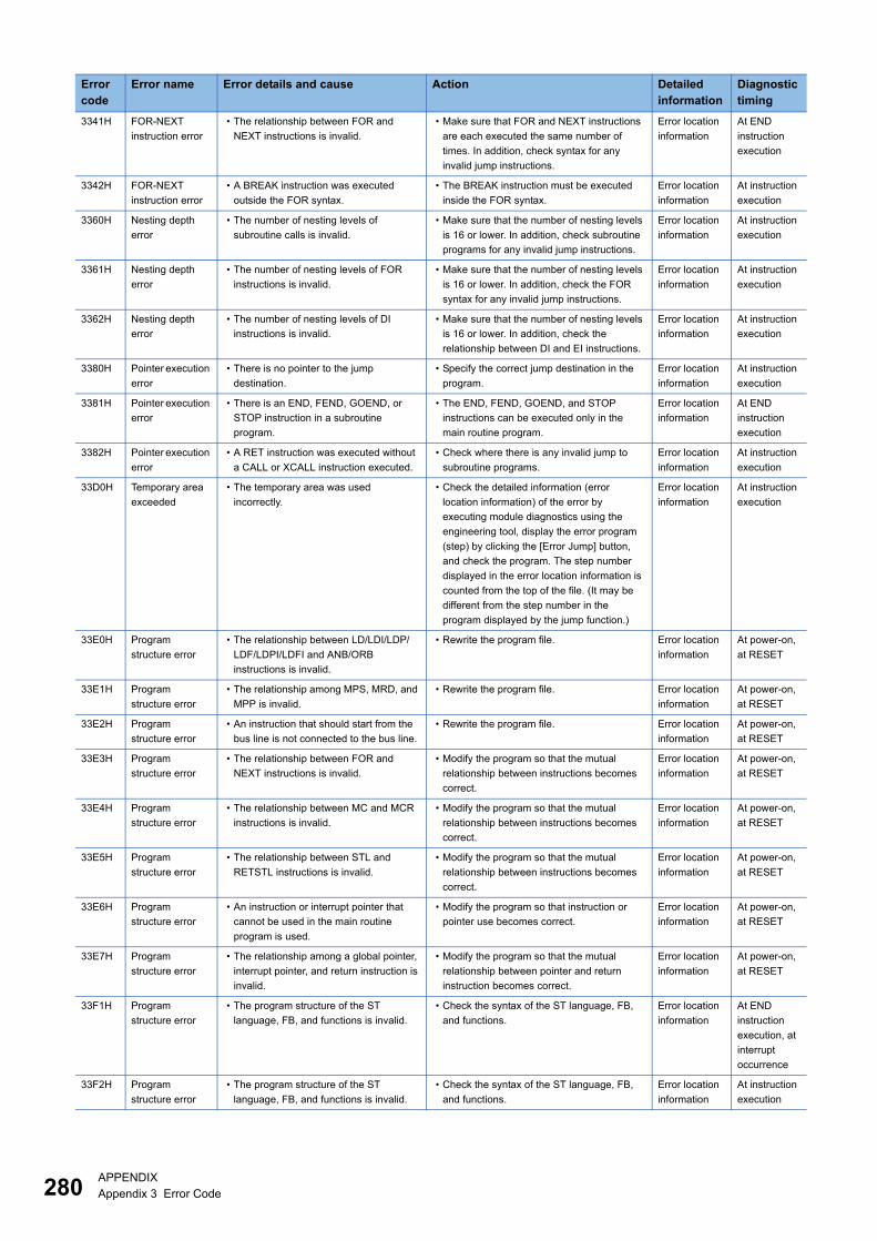
280APPENDIX
Appendix 3 Error Code
3341H FOR-NEXT
instruction error
� The relationship between FOR and
NEXT instructions is invalid.
� Make sure that FOR and NEXT instructions
are each executed the same number of
times. In addition, check syntax for any
invalid jump instructions.
Error location
information
At END
instruction
execution
3342H FOR-NEXT
instruction error
� A BREAK instruction was executed
outside the FOR syntax.
� The BREAK instruction must be executed
inside the FOR syntax.
Error location
information
At instruction
execution
3360H Nesting depth
error
� The number of nesting levels of
subroutine calls is invalid.
� Make sure that the number of nesting levels
is 16 or lower. In addition, check subroutine
programs for any invalid jump instructions.
Error location
information
At instruction
execution
3361H Nesting depth
error
� The number of nesting levels of FOR
instructions is invalid.
� Make sure that the number of nesting levels
is 16 or lower. In addition, check the FOR
syntax for any invalid jump instructions.
Error location
information
At instruction
execution
3362H Nesting depth
error
� The number of nesting levels of DI
instructions is invalid.
� Make sure that the number of nesting levels
is 16 or lower. In addition, check the
relationship between DI and EI instructions.
Error location
information
At instruction
execution
3380H Pointer execution
error
� There is no pointer to the jump
destination.
� Specify the correct jump destination in the
program.
Error location
information
At instruction
execution
3381H Pointer execution
error
� There is an END, FEND, GOEND, or
STOP instruction in a subroutine
program.
� The END, FEND, GOEND, and STOP
instructions can be executed only in the
main routine program.
Error location
information
At END
instruction
execution
3382H Pointer execution
error
� A RET instruction was executed without
a CALL or XCALL instruction executed.
� Check where there is any invalid jump to
subroutine programs.
Error location
information
At instruction
execution
33D0H Temporary area
exceeded
� The temporary area was used
incorrectly.
� Check the detailed information (error
location information) of the error by
executing module diagnostics using the
engineering tool, display the error program
(step) by clicking the [Error Jump] button,
and check the program. The step number
displayed in the error location information is
counted from the top of the file. (It may be
different from the step number in the
program displayed by the jump function.)
Error location
information
At instruction
execution
33E0H Program
structure error
� The relationship between LD/LDI/LDP/
LDF/LDPI/LDFI and ANB/ORB
instructions is invalid.
� Rewrite the program file. Error location
information
At power-on,
at RESET
33E1H Program
structure error
� The relationship among MPS, MRD, and
MPP is invalid.
� Rewrite the program file. Error location
information
At power-on,
at RESET
33E2H Program
structure error
� An instruction that should start from the
bus line is not connected to the bus line.
� Rewrite the program file. Error location
information
At power-on,
at RESET
33E3H Program
structure error
� The relationship between FOR and
NEXT instructions is invalid.
� Modify the program so that the mutual
relationship between instructions becomes
correct.
Error location
information
At power-on,
at RESET
33E4H Program
structure error
� The relationship between MC and MCR
instructions is invalid.
� Modify the program so that the mutual
relationship between instructions becomes
correct.
Error location
information
At power-on,
at RESET
33E5H Program
structure error
� The relationship between STL and
RETSTL instructions is invalid.
� Modify the program so that the mutual
relationship between instructions becomes
correct.
Error location
information
At power-on,
at RESET
33E6H Program
structure error
� An instruction or interrupt pointer that
cannot be used in the main routine
program is used.
� Modify the program so that instruction or
pointer use becomes correct.
Error location
information
At power-on,
at RESET
33E7H Program
structure error
� The relationship among a global pointer,
interrupt pointer, and return instruction is
invalid.
� Modify the program so that the mutual
relationship between pointer and return
instruction becomes correct.
Error location
information
At power-on,
at RESET
33F1H Program
structure error
� The program structure of the ST
language, FB, and functions is invalid.
� Check the syntax of the ST language, FB,
and functions.
Error location
information
At END
instruction
execution, at
interrupt
occurrence
33F2H Program
structure error
� The program structure of the ST
language, FB, and functions is invalid.
� Check the syntax of the ST language, FB,
and functions.
Error location
information
At instruction
execution
Error
code
Error name Error details and cause Action Detailed
information
Diagnostic
timing
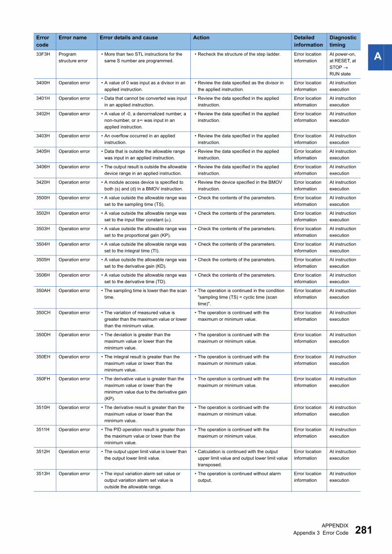
APPENDIX
Appendix 3 Error Code 281
A33F3H Program
structure error
� More than two STL instructions for the
same S number are programmed.
� Recheck the structure of the step ladder. Error location
information
At power-on,
at RESET, at
STOP
RUN state
3400H Operation error � A value of 0 was input as a divisor in an
applied instruction.
� Review the data specified as the divisor in
the applied instruction.
Error location
information
At instruction
execution
3401H Operation error � Data that cannot be converted was input
in an applied instruction.
� Review the data specified in the applied
instruction.
Error location
information
At instruction
execution
3402H Operation error � A value of -0, a denormalized number, a
non-number, or ±∞ was input in an
applied instruction.
� Review the data specified in the applied
instruction.
Error location
information
At instruction
execution
3403H Operation error � An overflow occurred in an applied
instruction.
� Review the data specified in the applied
instruction.
Error location
information
At instruction
execution
3405H Operation error � Data that is outside the allowable range
was input in an applied instruction.
� Review the data specified in the applied
instruction.
Error location
information
At instruction
execution
3406H Operation error � The output result is outside the allowable
device range in an applied instruction.
� Review the data specified in the applied
instruction.
Error location
information
At instruction
execution
3420H Operation error � A module access device is specified to
both (s) and (d) in a BMOV instruction.
� Review the device specified in the BMOV
instruction.
Error location
information
At instruction
execution
3500H Operation error � A value outside the allowable range was
set to the sampling time (TS).
� Check the contents of the parameters. Error location
information
At instruction
execution
3502H Operation error � A value outside the allowable range was
set to the input filter constant ().
� Check the contents of the parameters. Error location
information
At instruction
execution
3503H Operation error � A value outside the allowable range was
set to the proportional gain (KP).
� Check the contents of the parameters. Error location
information
At instruction
execution
3504H Operation error � A value outside the allowable range was
set to the integral time (TI).
� Check the contents of the parameters. Error location
information
At instruction
execution
3505H Operation error � A value outside the allowable range was
set to the derivative gain (KD).
� Check the contents of the parameters. Error location
information
At instruction
execution
3506H Operation error � A value outside the allowable range was
set to the derivative time (TD).
� Check the contents of the parameters. Error location
information
At instruction
execution
350AH Operation error � The sampling time is lower than the scan
time.
� The operation is continued in the condition
"sampling time (TS) = cyclic time (scan
time)".
Error location
information
At instruction
execution
350CH Operation error � The variation of measured value is
greater than the maximum value or lower
than the minimum value.
� The operation is continued with the
maximum or minimum value.
Error location
information
At instruction
execution
350DH Operation error � The deviation is greater than the
maximum value or lower than the
minimum value.
� The operation is continued with the
maximum or minimum value.
Error location
information
At instruction
execution
350EH Operation error � The integral result is greater than the
maximum value or lower than the
minimum value.
� The operation is continued with the
maximum or minimum value.
Error location
information
At instruction
execution
350FH Operation error � The derivative value is greater than the
maximum value or lower than the
minimum value due to the derivative gain
(KP).
� The operation is continued with the
maximum or minimum value.
Error location
information
At instruction
execution
3510H Operation error � The derivative result is greater than the
maximum value or lower than the
minimum value.
� The operation is continued with the
maximum or minimum value.
Error location
information
At instruction
execution
3511H Operation error � The PID operation result is greater than
the maximum value or lower than the
minimum value.
� The operation is continued with the
maximum or minimum value.
Error location
information
At instruction
execution
3512H Operation error � The output upper limit value is lower than
the output lower limit value.
� Calculation is continued with the output
upper limit value and output lower limit value
transposed.
Error location
information
At instruction
execution
3513H Operation error � The input variation alarm set value or
output variation alarm set value is
outside the allowable range.
� The operation is continued without alarm
output.
Error location
information
At instruction
execution
Error
code
Error name Error details and cause Action Detailed
information
Diagnostic
timing
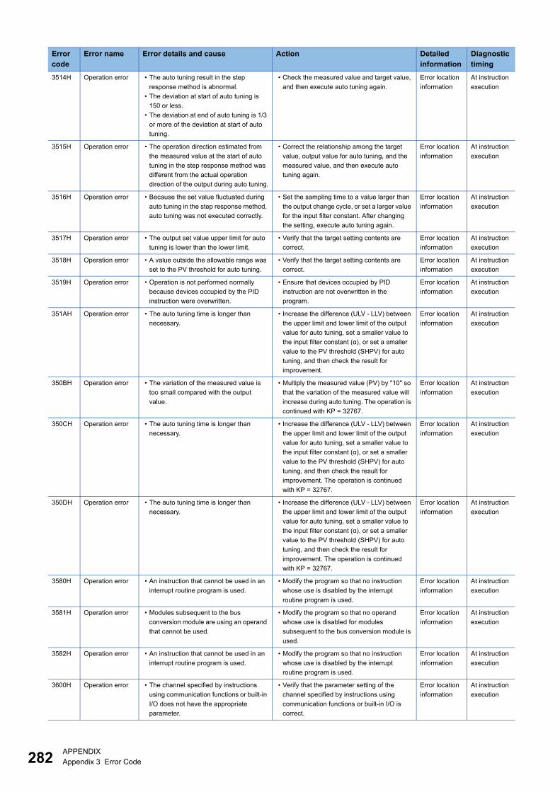
282APPENDIX
Appendix 3 Error Code
3514H Operation error � The auto tuning result in the step
response method is abnormal.
� The deviation at start of auto tuning is
150 or less.
� The deviation at end of auto tuning is 1/3
or more of the deviation at start of auto
tuning.
� Check the measured value and target value,
and then execute auto tuning again.
Error location
information
At instruction
execution
3515H Operation error � The operation direction estimated from
the measured value at the start of auto
tuning in the step response method was
different from the actual operation
direction of the output during auto tuning.
� Correct the relationship among the target
value, output value for auto tuning, and the
measured value, and then execute auto
tuning again.
Error location
information
At instruction
execution
3516H Operation error � Because the set value fluctuated during
auto tuning in the step response method,
auto tuning was not executed correctly.
� Set the sampling time to a value larger than
the output change cycle, or set a larger value
for the input filter constant. After changing
the setting, execute auto tuning again.
Error location
information
At instruction
execution
3517H Operation error � The output set value upper limit for auto
tuning is lower than the lower limit.
� Verify that the target setting contents are
correct.
Error location
information
At instruction
execution
3518H Operation error � A value outside the allowable range was
set to the PV threshold for auto tuning.
� Verify that the target setting contents are
correct.
Error location
information
At instruction
execution
3519H Operation error � Operation is not performed normally
because devices occupied by the PID
instruction were overwritten.
� Ensure that devices occupied by PID
instruction are not overwritten in the
program.
Error location
information
At instruction
execution
351AH Operation error � The auto tuning time is longer than
necessary.
� Increase the difference (ULV - LLV) between
the upper limit and lower limit of the output
value for auto tuning, set a smaller value to
the input filter constant (α), or set a smaller
value to the PV threshold (SHPV) for auto
tuning, and then check the result for
improvement.
Error location
information
At instruction
execution
350BH Operation error � The variation of the measured value is
too small compared with the output
value.
� Multiply the measured value (PV) by "10" so
that the variation of the measured value will
increase during auto tuning. The operation is
continued with KP = 32767.
Error location
information
At instruction
execution
350CH Operation error � The auto tuning time is longer than
necessary.
� Increase the difference (ULV - LLV) between
the upper limit and lower limit of the output
value for auto tuning, set a smaller value to
the input filter constant (α), or set a smaller
value to the PV threshold (SHPV) for auto
tuning, and then check the result for
improvement. The operation is continued
with KP = 32767.
Error location
information
At instruction
execution
350DH Operation error � The auto tuning time is longer than
necessary.
� Increase the difference (ULV - LLV) between
the upper limit and lower limit of the output
value for auto tuning, set a smaller value to
the input filter constant (α), or set a smaller
value to the PV threshold (SHPV) for auto
tuning, and then check the result for
improvement. The operation is continued
with KP = 32767.
Error location
information
At instruction
execution
3580H Operation error � An instruction that cannot be used in an
interrupt routine program is used.
� Modify the program so that no instruction
whose use is disabled by the interrupt
routine program is used.
Error location
information
At instruction
execution
3581H Operation error � Modules subsequent to the bus
conversion module are using an operand
that cannot be used.
� Modify the program so that no operand
whose use is disabled for modules
subsequent to the bus conversion module is
used.
Error location
information
At instruction
execution
3582H Operation error � An instruction that cannot be used in an
interrupt routine program is used.
� Modify the program so that no instruction
whose use is disabled by the interrupt
routine program is used.
Error location
information
At instruction
execution
3600H Operation error � The channel specified by instructions
using communication functions or built-in
I/O does not have the appropriate
parameter.
� Verify that the parameter setting of the
channel specified by instructions using
communication functions or built-in I/O is
correct.
Error location
information
At instruction
execution
Error
code
Error name Error details and cause Action Detailed
information
Diagnostic
timing
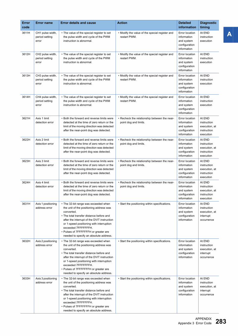
APPENDIX
Appendix 3 Error Code 283
A3611H CH1 pulse width,
period setting
error
� The value of the special register to set
the pulse width and cycle of the PWM
instruction is abnormal.
� Modify the value of the special register and
restart PWM.
Error location
information
and system
configuration
information
At END
instruction
execution
3612H CH2 pulse width,
period setting
error
� The value of the special register to set
the pulse width and cycle of the PWM
instruction is abnormal.
� Modify the value of the special register and
restart PWM.
Error location
information
and system
configuration
information
At END
instruction
execution
3613H CH3 pulse width,
period setting
error
� The value of the special register to set
the pulse width and cycle of the PWM
instruction is abnormal.
� Modify the value of the special register and
restart PWM.
Error location
information
and system
configuration
information
At END
instruction
execution
3614H CH4 pulse width,
period setting
error
� The value of the special register to set
the pulse width and cycle of the PWM
instruction is abnormal.
� Modify the value of the special register and
restart PWM.
Error location
information
and system
configuration
information
At END
instruction
execution
3621H Axis 1 limit
detection error
� Both the forward and reverse limits were
detected at the time of zero return or the
limit of the moving direction was detected
after the near-point dog was detected.
� Recheck the relationship between the near-
point dog and limits.
Error location
information
and system
configuration
information
At END
instruction
execution, at
instruction
execution
3622H Axis 2 limit
detection error
� Both the forward and reverse limits were
detected at the time of zero return or the
limit of the moving direction was detected
after the near-point dog was detected.
� Recheck the relationship between the near-
point dog and limits.
Error location
information
and system
configuration
information
At END
instruction
execution, at
instruction
execution
3623H Axis 3 limit
detection error
� Both the forward and reverse limits were
detected at the time of zero return or the
limit of the moving direction was detected
after the near-point dog was detected.
� Recheck the relationship between the near-
point dog and limits.
Error location
information
and system
configuration
information
At END
instruction
execution, at
instruction
execution
3624H Axis 4 limit
detection error
� Both the forward and reverse limits were
detected at the time of zero return or the
limit of the moving direction was detected
after the near-point dog was detected.
� Recheck the relationship between the near-
point dog and limits.
Error location
information
and system
configuration
information
At END
instruction
execution, at
instruction
execution
3631H Axis 1 positioning
address error
� The 32-bit range was exceeded when
the unit of the positioning address was
converted.
� The total transfer distance before and
after the interrupt of the DVIT instruction
or 1-speed positioning with interruption
exceeded 7FFFFFFFH.
� Pulses of 7FFFFFFFH or greater are
needed to specify an absolute address.
� Start the positioning within specifications. Error location
information
and system
configuration
information
At END
instruction
execution, at
interrupt
occurrence
3632H Axis 2 positioning
address error
� The 32-bit range was exceeded when
the unit of the positioning address was
converted.
� The total transfer distance before and
after the interrupt of the DVIT instruction
or 1-speed positioning with interruption
exceeded 7FFFFFFFH.
� Pulses of 7FFFFFFFH or greater are
needed to specify an absolute address.
� Start the positioning within specifications. Error location
information
and system
configuration
information
At END
instruction
execution, at
interrupt
occurrence
3633H Axis 3 positioning
address error
� The 32-bit range was exceeded when
the unit of the positioning address was
converted.
� The total transfer distance before and
after the interrupt of the DVIT instruction
or 1-speed positioning with interruption
exceeded 7FFFFFFFH.
� Pulses of 7FFFFFFFH or greater are
needed to specify an absolute address.
� Start the positioning within specifications. Error location
information
and system
configuration
information
At END
instruction
execution, at
interrupt
occurrence
Error
code
Error name Error details and cause Action Detailed
information
Diagnostic
timing
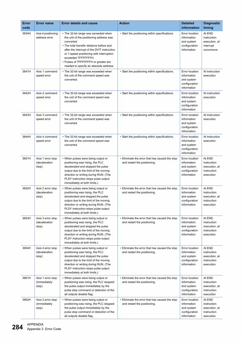
284APPENDIX
Appendix 3 Error Code
3634H Axis 4 positioning
address error
� The 32-bit range was exceeded when
the unit of the positioning address was
converted.
� The total transfer distance before and
after the interrupt of the DVIT instruction
or 1-speed positioning with interruption
exceeded 7FFFFFFFH.
� Pulses of 7FFFFFFFH or greater are
needed to specify an absolute address.
� Start the positioning within specifications. Error location
information
and system
configuration
information
At END
instruction
execution, at
interrupt
occurrence
3641H Axis 1 command
speed error
� The 32-bit range was exceeded when
the unit of the command speed was
converted.
� Start the positioning within specifications. Error location
information
and system
configuration
information
At instruction
execution
3642H Axis 2 command
speed error
� The 32-bit range was exceeded when
the unit of the command speed was
converted.
� Start the positioning within specifications. Error location
information
and system
configuration
information
At instruction
execution
3643H Axis 3 command
speed error
� The 32-bit range was exceeded when
the unit of the command speed was
converted.
� Start the positioning within specifications. Error location
information
and system
configuration
information
At instruction
execution
3644H Axis 4 command
speed error
� The 32-bit range was exceeded when
the unit of the command speed was
converted.
� Start the positioning within specifications. Error location
information
and system
configuration
information
At instruction
execution
3651H Axis 1 error stop
(deceleration
stop)
� When pulses were being output or
positioning was rising, the PLC
decelerated and stopped the pulse
output due to the limit of the moving
direction or writing during RUN. (The
PLSY instruction stops pulse output
immediately at both limits.)
� Eliminate the error that has caused the stop
and restart the positioning.
Error location
information
and system
configuration
information
At END
instruction
execution, at
instruction
execution
3652H Axis 2 error stop
(deceleration
stop)
� When pulses were being output or
positioning was rising, the PLC
decelerated and stopped the pulse
output due to the limit of the moving
direction or writing during RUN. (The
PLSY instruction stops pulse output
immediately at both limits.)
� Eliminate the error that has caused the stop
and restart the positioning.
Error location
information
and system
configuration
information
At END
instruction
execution, at
instruction
execution
3653H Axis 3 error stop
(deceleration
stop)
� When pulses were being output or
positioning was rising, the PLC
decelerated and stopped the pulse
output due to the limit of the moving
direction or writing during RUN. (The
PLSY instruction stops pulse output
immediately at both limits.)
� Eliminate the error that has caused the stop
and restart the positioning.
Error location
information
and system
configuration
information
At END
instruction
execution, at
instruction
execution
3654H Axis 4 error stop
(deceleration
stop)
� When pulses were being output or
positioning was rising, the PLC
decelerated and stopped the pulse
output due to the limit of the moving
direction or writing during RUN. (The
PLSY instruction stops pulse output
immediately at both limits.)
� Eliminate the error that has caused the stop
and restart the positioning.
Error location
information
and system
configuration
information
At END
instruction
execution, at
instruction
execution
3661H Axis 1 error stop
(immediately
stop)
� When pulses were being output or
positioning was rising, the PLC stopped
the pulse output immediately by the
pulse stop command or detection of the
all outputs disable flag.
� Eliminate the error that has caused the stop
and restart the positioning.
Error location
information
and system
configuration
information
At END
instruction
execution, at
instruction
execution
3662H Axis 2 error stop
(immediately
stop)
� When pulses were being output or
positioning was rising, the PLC stopped
the pulse output immediately by the
pulse stop command or detection of the
all outputs disable flag.
� Eliminate the error that has caused the stop
and restart the positioning.
Error location
information
and system
configuration
information
At END
instruction
execution, at
instruction
execution
Error
code
Error name Error details and cause Action Detailed
information
Diagnostic
timing
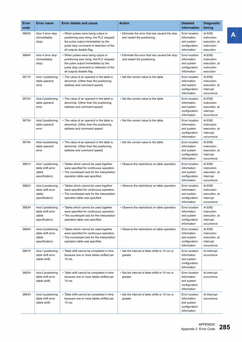
APPENDIX
Appendix 3 Error Code 285
A3663H Axis 3 error stop
(immediately
stop)
� When pulses were being output or
positioning was rising, the PLC stopped
the pulse output immediately by the
pulse stop command or detection of the
all outputs disable flag.
� Eliminate the error that has caused the stop
and restart the positioning.
Error location
information
and system
configuration
information
At END
instruction
execution, at
instruction
execution
3664H Axis 4 error stop
(immediately
stop)
� When pulses were being output or
positioning was rising, the PLC stopped
the pulse output immediately by the
pulse stop command or detection of the
all outputs disable flag.
� Eliminate the error that has caused the stop
and restart the positioning.
Error location
information
and system
configuration
information
At END
instruction
execution, at
instruction
execution
3671H Axis 1 positioning
table operand
error
� The value of an operand in the table is
abnormal. (Other than the positioning
address and command speed)
� Set the correct value to the table. Error location
information
and system
configuration
information
At END
instruction
execution, at
interrupt
occurrence
3672H Axis 2 positioning
table operand
error
� The value of an operand in the table is
abnormal. (Other than the positioning
address and command speed)
� Set the correct value to the table. Error location
information
and system
configuration
information
At END
instruction
execution, at
interrupt
occurrence
3673H Axis 3 positioning
table operand
error
� The value of an operand in the table is
abnormal. (Other than the positioning
address and command speed)
� Set the correct value to the table. Error location
information
and system
configuration
information
At END
instruction
execution, at
interrupt
occurrence
3674H Axis 4 positioning
table operand
error
� The value of an operand in the table is
abnormal. (Other than the positioning
address and command speed)
� Set the correct value to the table. Error location
information
and system
configuration
information
At END
instruction
execution, at
interrupt
occurrence
3681H Axis 1 positioning
table shift error
(table
specification)
� Tables which cannot be used together
were specified for continuous operation.
� The counterpart axis for the interpolation
operation table was specified.
� Observe the restrictions on table operation. Error location
information
and system
configuration
information
At END
instruction
execution, at
interrupt
occurrence
3682H Axis 2 positioning
table shift error
(table
specification)
� Tables which cannot be used together
were specified for continuous operation.
� The counterpart axis for the interpolation
operation table was specified.
� Observe the restrictions on table operation. Error location
information
and system
configuration
information
At END
instruction
execution, at
interrupt
occurrence
3683H Axis 3 positioning
table shift error
(table
specification)
� Tables which cannot be used together
were specified for continuous operation.
� The counterpart axis for the interpolation
operation table was specified.
� Observe the restrictions on table operation. Error location
information
and system
configuration
information
At END
instruction
execution, at
interrupt
occurrence
3684H Axis 4 positioning
table shift error
(table
specification)
� Tables which cannot be used together
were specified for continuous operation.
� The counterpart axis for the interpolation
operation table was specified.
� Observe the restrictions on table operation. Error location
information
and system
configuration
information
At END
instruction
execution, at
interrupt
occurrence
3691H Axis 1 positioning
table shift error
(table shift)
� Table shift cannot be completed in time
because one or more tables shifted per
10 ms.
� Set the interval of table shifts to 10 ms or
greater.
Error location
information
and system
configuration
information
At interrupt
occurrence
3692H Axis 2 positioning
table shift error
(table shift)
� Table shift cannot be completed in time
because one or more tables shifted per
10 ms.
� Set the interval of table shifts to 10 ms or
greater.
Error location
information
and system
configuration
information
At interrupt
occurrence
3693H Axis 3 positioning
table shift error
(table shift)
� Table shift cannot be completed in time
because one or more tables shifted per
10 ms.
� Set the interval of table shifts to 10 ms or
greater.
Error location
information
and system
configuration
information
At interrupt
occurrence
Error
code
Error name Error details and cause Action Detailed
information
Diagnostic
timing
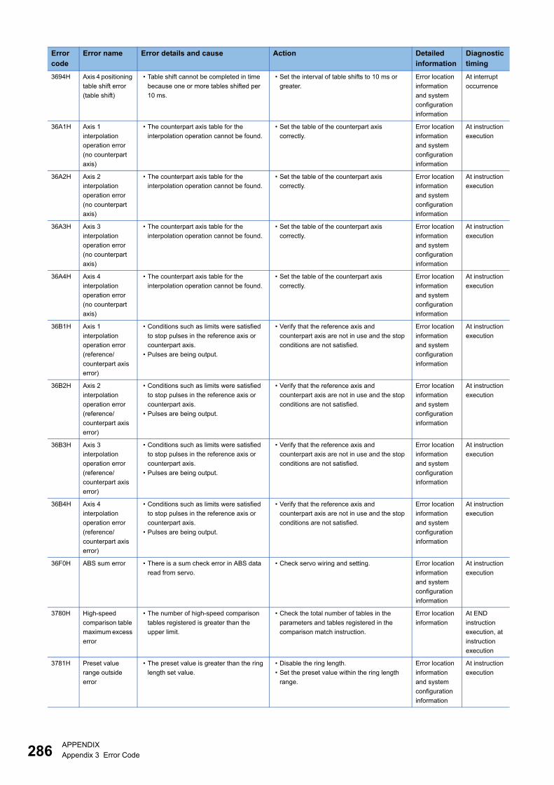
286APPENDIX
Appendix 3 Error Code
3694H Axis 4 positioning
table shift error
(table shift)
� Table shift cannot be completed in time
because one or more tables shifted per
10 ms.
� Set the interval of table shifts to 10 ms or
greater.
Error location
information
and system
configuration
information
At interrupt
occurrence
36A1H Axis 1
interpolation
operation error
(no counterpart
axis)
� The counterpart axis table for the
interpolation operation cannot be found.
� Set the table of the counterpart axis
correctly.
Error location
information
and system
configuration
information
At instruction
execution
36A2H Axis 2
interpolation
operation error
(no counterpart
axis)
� The counterpart axis table for the
interpolation operation cannot be found.
� Set the table of the counterpart axis
correctly.
Error location
information
and system
configuration
information
At instruction
execution
36A3H Axis 3
interpolation
operation error
(no counterpart
axis)
� The counterpart axis table for the
interpolation operation cannot be found.
� Set the table of the counterpart axis
correctly.
Error location
information
and system
configuration
information
At instruction
execution
36A4H Axis 4
interpolation
operation error
(no counterpart
axis)
� The counterpart axis table for the
interpolation operation cannot be found.
� Set the table of the counterpart axis
correctly.
Error location
information
and system
configuration
information
At instruction
execution
36B1H Axis 1
interpolation
operation error
(reference/
counterpart axis
error)
� Conditions such as limits were satisfied
to stop pulses in the reference axis or
counterpart axis.
� Pulses are being output.
� Verify that the reference axis and
counterpart axis are not in use and the stop
conditions are not satisfied.
Error location
information
and system
configuration
information
At instruction
execution
36B2H Axis 2
interpolation
operation error
(reference/
counterpart axis
error)
� Conditions such as limits were satisfied
to stop pulses in the reference axis or
counterpart axis.
� Pulses are being output.
� Verify that the reference axis and
counterpart axis are not in use and the stop
conditions are not satisfied.
Error location
information
and system
configuration
information
At instruction
execution
36B3H Axis 3
interpolation
operation error
(reference/
counterpart axis
error)
� Conditions such as limits were satisfied
to stop pulses in the reference axis or
counterpart axis.
� Pulses are being output.
� Verify that the reference axis and
counterpart axis are not in use and the stop
conditions are not satisfied.
Error location
information
and system
configuration
information
At instruction
execution
36B4H Axis 4
interpolation
operation error
(reference/
counterpart axis
error)
� Conditions such as limits were satisfied
to stop pulses in the reference axis or
counterpart axis.
� Pulses are being output.
� Verify that the reference axis and
counterpart axis are not in use and the stop
conditions are not satisfied.
Error location
information
and system
configuration
information
At instruction
execution
36F0H ABS sum error � There is a sum check error in ABS data
read from servo.
� Check servo wiring and setting. Error location
information
and system
configuration
information
At instruction
execution
3780H High-speed
comparison table
maximum excess
error
� The number of high-speed comparison
tables registered is greater than the
upper limit.
� Check the total number of tables in the
parameters and tables registered in the
comparison match instruction.
Error location
information
At END
instruction
execution, at
instruction
execution
3781H Preset value
range outside
error
� The preset value is greater than the ring
length set value.
� Disable the ring length.
� Set the preset value within the ring length
range.
Error location
information
and system
configuration
information
At instruction
execution
Error
code
Error name Error details and cause Action Detailed
information
Diagnostic
timing
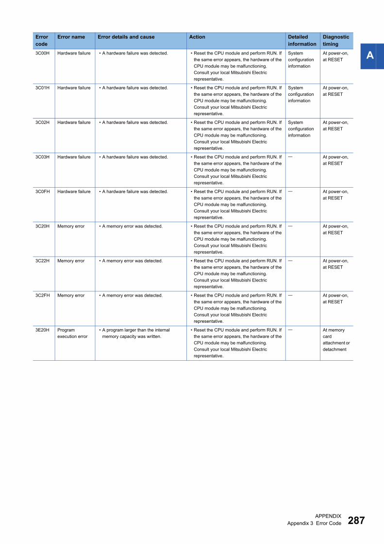
APPENDIX
Appendix 3 Error Code 287
A3C00H Hardware failure � A hardware failure was detected. � Reset the CPU module and perform RUN. If
the same error appears, the hardware of the
CPU module may be malfunctioning.
Consult your local Mitsubishi Electric
representative.
System
configuration
information
At power-on,
at RESET
3C01H Hardware failure � A hardware failure was detected. � Reset the CPU module and perform RUN. If
the same error appears, the hardware of the
CPU module may be malfunctioning.
Consult your local Mitsubishi Electric
representative.
System
configuration
information
At power-on,
at RESET
3C02H Hardware failure � A hardware failure was detected. � Reset the CPU module and perform RUN. If
the same error appears, the hardware of the
CPU module may be malfunctioning.
Consult your local Mitsubishi Electric
representative.
System
configuration
information
At power-on,
at RESET
3C03H Hardware failure � A hardware failure was detected. � Reset the CPU module and perform RUN. If
the same error appears, the hardware of the
CPU module may be malfunctioning.
Consult your local Mitsubishi Electric
representative.
At power-on,
at RESET
3C0FH Hardware failure � A hardware failure was detected. � Reset the CPU module and perform RUN. If
the same error appears, the hardware of the
CPU module may be malfunctioning.
Consult your local Mitsubishi Electric
representative.
At power-on,
at RESET
3C20H Memory error � A memory error was detected. � Reset the CPU module and perform RUN. If
the same error appears, the hardware of the
CPU module may be malfunctioning.
Consult your local Mitsubishi Electric
representative.
At power-on,
at RESET
3C22H Memory error � A memory error was detected. � Reset the CPU module and perform RUN. If
the same error appears, the hardware of the
CPU module may be malfunctioning.
Consult your local Mitsubishi Electric
representative.
At power-on,
at RESET
3C2FH Memory error � A memory error was detected. � Reset the CPU module and perform RUN. If
the same error appears, the hardware of the
CPU module may be malfunctioning.
Consult your local Mitsubishi Electric
representative.
At power-on,
at RESET
3E20H Program
execution error
� A program larger than the internal
memory capacity was written.
� Reset the CPU module and perform RUN. If
the same error appears, the hardware of the
CPU module may be malfunctioning.
Consult your local Mitsubishi Electric
representative.
At memory
card
attachment or
detachment
Error
code
Error name Error details and cause Action Detailed
information
Diagnostic
timing
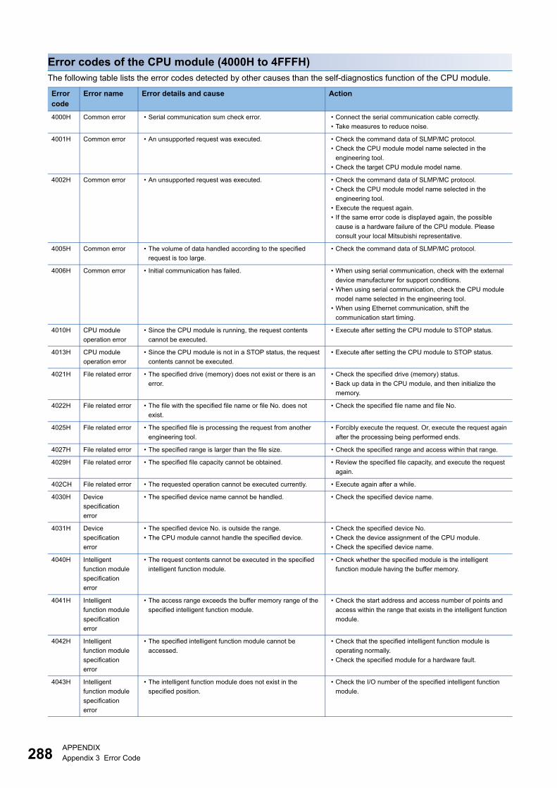
288APPENDIX
Appendix 3 Error Code
Error codes of the CPU module (4000H to 4FFFH)
The following table lists the error codes detected by other causes than the self-diagnostics function of the CPU module.
Error
code
Error name Error details and cause Action
4000H Common error � Serial communication sum check error. � Connect the serial communication cable correctly.
� Take measures to reduce noise.
4001H Common error � An unsupported request was executed. � Check the command data of SLMP/MC protocol.
� Check the CPU module model name selected in the
engineering tool.
� Check the target CPU module model name.
4002H Common error � An unsupported request was executed. � Check the command data of SLMP/MC protocol.
� Check the CPU module model name selected in the
engineering tool.
� Execute the request again.
� If the same error code is displayed again, the possible
cause is a hardware failure of the CPU module. Please
consult your local Mitsubishi representative.
4005H Common error � The volume of data handled according to the specified
request is too large.
� Check the command data of SLMP/MC protocol.
4006H Common error � Initial communication has failed. � When using serial communication, check with the external
device manufacturer for support conditions.
� When using serial communication, check the CPU module
model name selected in the engineering tool.
� When using Ethernet communication, shift the
communication start timing.
4010H CPU module
operation error
� Since the CPU module is running, the request contents
cannot be executed.
� Execute after setting the CPU module to STOP status.
4013H CPU module
operation error
� Since the CPU module is not in a STOP status, the request
contents cannot be executed.
� Execute after setting the CPU module to STOP status.
4021H File related error � The specified drive (memory) does not exist or there is an
error.
� Check the specified drive (memory) status.
� Back up data in the CPU module, and then initialize the
memory.
4022H File related error � The file with the specified file name or file No. does not
exist.
� Check the specified file name and file No.
4025H File related error � The specified file is processing the request from another
engineering tool.
� Forcibly execute the request. Or, execute the request again
after the processing being performed ends.
4027H File related error � The specified range is larger than the file size. � Check the specified range and access within that range.
4029H File related error � The specified file capacity cannot be obtained. � Review the specified file capacity, and execute the request
again.
402CH File related error � The requested operation cannot be executed currently. � Execute again after a while.
4030H Device
specification
error
� The specified device name cannot be handled. � Check the specified device name.
4031H Device
specification
error
� The specified device No. is outside the range.
� The CPU module cannot handle the specified device.
� Check the specified device No.
� Check the device assignment of the CPU module.
� Check the specified device name.
4040H Intelligent
function module
specification
error
� The request contents cannot be executed in the specified
intelligent function module.
� Check whether the specified module is the intelligent
function module having the buffer memory.
4041H Intelligent
function module
specification
error
� The access range exceeds the buffer memory range of the
specified intelligent function module.
� Check the start address and access number of points and
access within the range that exists in the intelligent function
module.
4042H Intelligent
function module
specification
error
� The specified intelligent function module cannot be
accessed.
� Check that the specified intelligent function module is
operating normally.
� Check the specified module for a hardware fault.
4043H Intelligent
function module
specification
error
� The intelligent function module does not exist in the
specified position.
� Check the I/O number of the specified intelligent function
module.
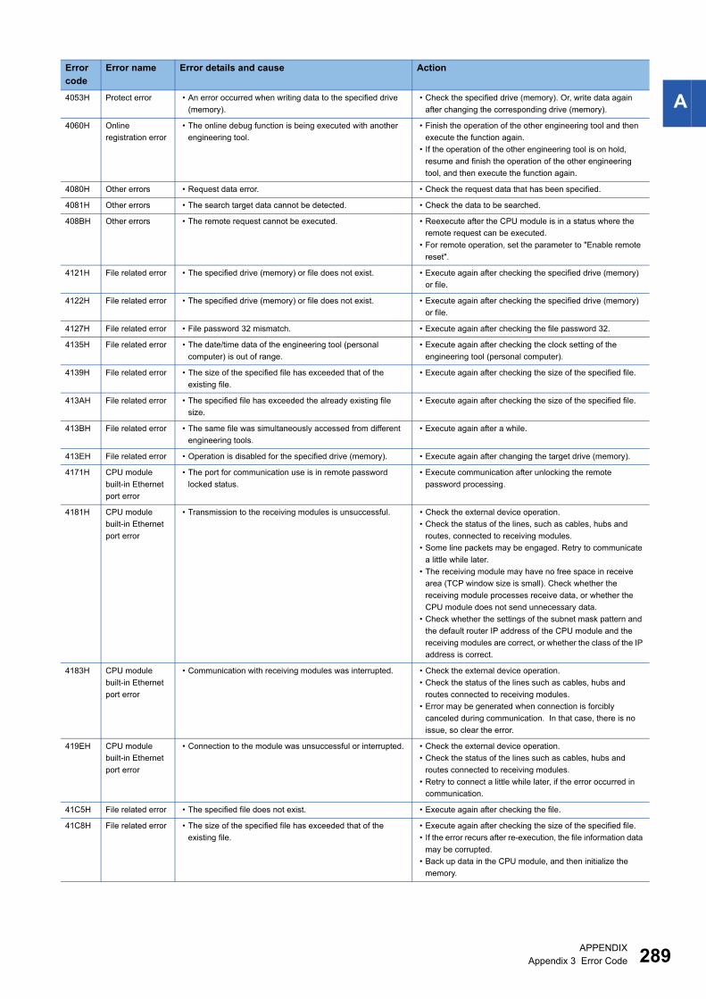
APPENDIX
Appendix 3 Error Code 289
A4053H Protect error � An error occurred when writing data to the specified drive
(memory).
� Check the specified drive (memory). Or, write data again
after changing the corresponding drive (memory).
4060H Online
registration error
� The online debug function is being executed with another
engineering tool.
� Finish the operation of the other engineering tool and then
execute the function again.
� If the operation of the other engineering tool is on hold,
resume and finish the operation of the other engineering
tool, and then execute the function again.
4080H Other errors � Request data error. � Check the request data that has been specified.
4081H Other errors � The search target data cannot be detected. � Check the data to be searched.
408BH Other errors � The remote request cannot be executed. � Reexecute after the CPU module is in a status where the
remote request can be executed.
� For remote operation, set the parameter to "Enable remote
reset".
4121H File related error � The specified drive (memory) or file does not exist. � Execute again after checking the specified drive (memory)
or file.
4122H File related error � The specified drive (memory) or file does not exist. � Execute again after checking the specified drive (memory)
or file.
4127H File related error � File password 32 mismatch. � Execute again after checking the file password 32.
4135H File related error � The date/time data of the engineering tool (personal
computer) is out of range.
� Execute again after checking the clock setting of the
engineering tool (personal computer).
4139H File related error � The size of the specified file has exceeded that of the
existing file.
� Execute again after checking the size of the specified file.
413AH File related error � The specified file has exceeded the already existing file
size.
� Execute again after checking the size of the specified file.
413BH File related error � The same file was simultaneously accessed from different
engineering tools.
� Execute again after a while.
413EH File related error � Operation is disabled for the specified drive (memory). � Execute again after changing the target drive (memory).
4171H CPU module
built-in Ethernet
port error
� The port for communication use is in remote password
locked status.
� Execute communication after unlocking the remote
password processing.
4181H CPU module
built-in Ethernet
port error
� Transmission to the receiving modules is unsuccessful. � Check the external device operation.
� Check the status of the lines, such as cables, hubs and
routes, connected to receiving modules.
� Some line packets may be engaged. Retry to communicate
a little while later.
� The receiving module may have no free space in receive
area (TCP window size is small). Check whether the
receiving module processes receive data, or whether the
CPU module does not send unnecessary data.
� Check whether the settings of the subnet mask pattern and
the default router IP address of the CPU module and the
receiving modules are correct, or whether the class of the IP
address is correct.
4183H CPU module
built-in Ethernet
port error
� Communication with receiving modules was interrupted. � Check the external device operation.
� Check the status of the lines such as cables, hubs and
routes connected to receiving modules.
� Error may be generated when connection is forcibly
canceled during communication. In that case, there is no
issue, so clear the error.
419EH CPU module
built-in Ethernet
port error
� Connection to the module was unsuccessful or interrupted. � Check the external device operation.
� Check the status of the lines such as cables, hubs and
routes connected to receiving modules.
� Retry to connect a little while later, if the error occurred in
communication.
41C5H File related error � The specified file does not exist. � Execute again after checking the file.
41C8H File related error � The size of the specified file has exceeded that of the
existing file.
� Execute again after checking the size of the specified file.
� If the error recurs after re-execution, the file information data
may be corrupted.
� Back up data in the CPU module, and then initialize the
memory.
Error
code
Error name Error details and cause Action
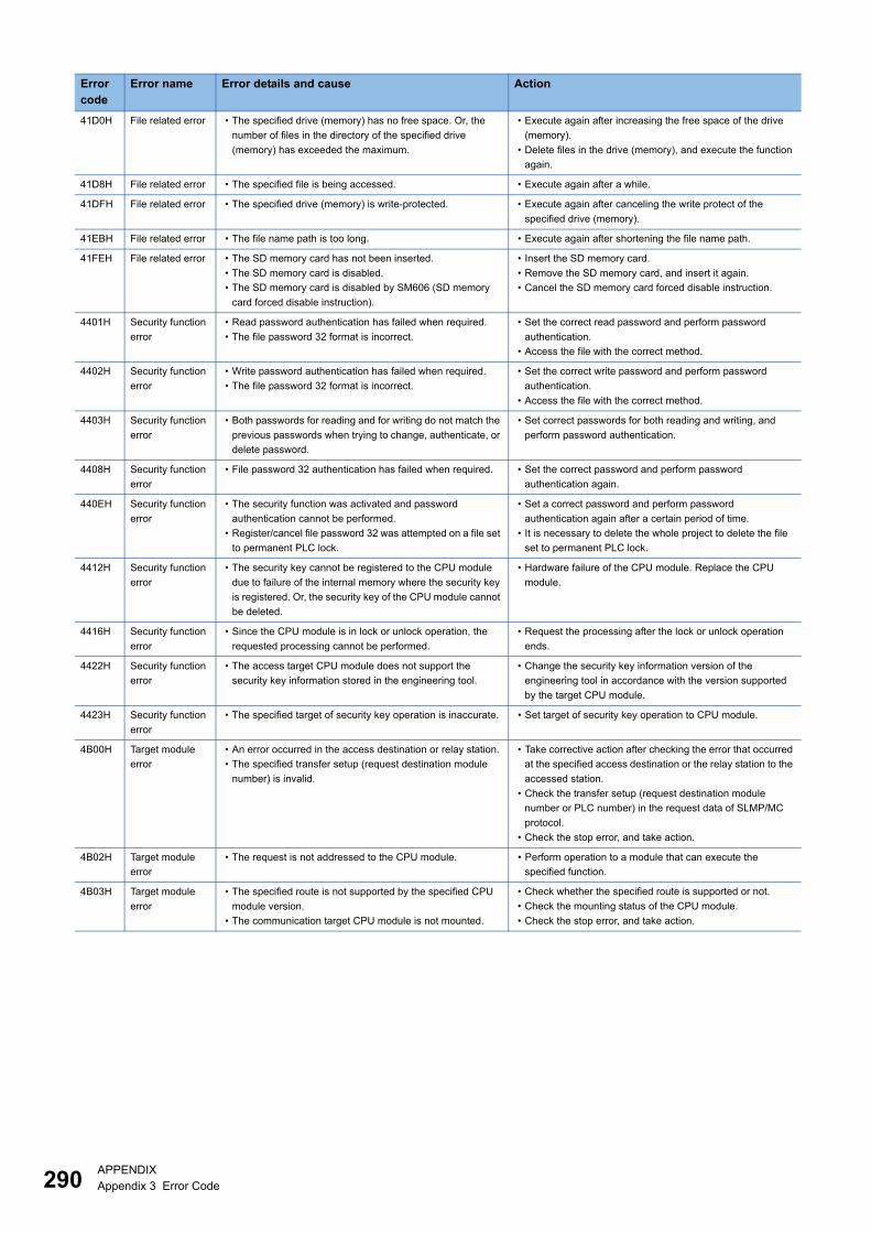
290APPENDIX
Appendix 3 Error Code
41D0H File related error � The specified drive (memory) has no free space. Or, the
number of files in the directory of the specified drive
(memory) has exceeded the maximum.
� Execute again after increasing the free space of the drive
(memory).
� Delete files in the drive (memory), and execute the function
again.
41D8H File related error � The specified file is being accessed. � Execute again after a while.
41DFH File related error � The specified drive (memory) is write-protected. � Execute again after canceling the write protect of the
specified drive (memory).
41EBH File related error � The file name path is too long. � Execute again after shortening the file name path.
41FEH File related error � The SD memory card has not been inserted.
� The SD memory card is disabled.
� The SD memory card is disabled by SM606 (SD memory
card forced disable instruction).
� Insert the SD memory card.
� Remove the SD memory card, and insert it again.
� Cancel the SD memory card forced disable instruction.
4401H Security function
error
� Read password authentication has failed when required.
� The file password 32 format is incorrect.
� Set the correct read password and perform password
authentication.
� Access the file with the correct method.
4402H Security function
error
� Write password authentication has failed when required.
� The file password 32 format is incorrect.
� Set the correct write password and perform password
authentication.
� Access the file with the correct method.
4403H Security function
error
� Both passwords for reading and for writing do not match the
previous passwords when trying to change, authenticate, or
delete password.
� Set correct passwords for both reading and writing, and
perform password authentication.
4408H Security function
error
� File password 32 authentication has failed when required. � Set the correct password and perform password
authentication again.
440EH Security function
error
� The security function was activated and password
authentication cannot be performed.
� Register/cancel file password 32 was attempted on a file set
to permanent PLC lock.
� Set a correct password and perform password
authentication again after a certain period of time.
� It is necessary to delete the whole project to delete the file
set to permanent PLC lock.
4412H Security function
error
� The security key cannot be registered to the CPU module
due to failure of the internal memory where the security key
is registered. Or, the security key of the CPU module cannot
be deleted.
� Hardware failure of the CPU module. Replace the CPU
module.
4416H Security function
error
� Since the CPU module is in lock or unlock operation, the
requested processing cannot be performed.
� Request the processing after the lock or unlock operation
ends.
4422H Security function
error
� The access target CPU module does not support the
security key information stored in the engineering tool.
� Change the security key information version of the
engineering tool in accordance with the version supported
by the target CPU module.
4423H Security function
error
� The specified target of security key operation is inaccurate. � Set target of security key operation to CPU module.
4B00H Target module
error
� An error occurred in the access destination or relay station.
� The specified transfer setup (request destination module
number) is invalid.
� Take corrective action after checking the error that occurred
at the specified access destination or the relay station to the
accessed station.
� Check the transfer setup (request destination module
number or PLC number) in the request data of SLMP/MC
protocol.
� Check the stop error, and take action.
4B02H Target module
error
� The request is not addressed to the CPU module. � Perform operation to a module that can execute the
specified function.
4B03H Target module
error
� The specified route is not supported by the specified CPU
module version.
� The communication target CPU module is not mounted.
� Check whether the specified route is supported or not.
� Check the mounting status of the CPU module.
� Check the stop error, and take action.
Error
code
Error name Error details and cause Action

APPENDIX
Appendix 4 Parameter List 291
A
Appendix 4 Parameter List
A parameter list is shown below.
System parameters
CPU parameters
Classification-Level 1 Classification-Level 2 Classification-Level 3
I/O Assignment Setting Model Name
Intelligent Module No.
Serial Communication ch
CPU Module Operation at Error Detection
Classification-Level 1 Classification-Level 2 Classification-Level 3
Name Setting Title Setting Title
Comment Setting Comment
Operation Related Setting RUN Contact Setting RUN
Contact Operation
Remote Reset Setting Remote Reset
Clock Related Setting Time Zone
Comment
Interrupt Settings Fixed Scan Interval Setting Interrupt Setting from Internal Timer
Fixed Scan Execution Mode Setting Fixed Scan Execution Mode
Interrupt Priority Setting from Module Multiple Interrupt
Interrupt Priority
Index Register Save/Restoration
Service Processing Setting Device/Label Access Service Processing Setting Specifying Method
File Setting Initial Value Setting Setting of Device Initial Value Use Or Not
Target Memory
Global Device Initial Value File Name
Memory/Device Setting Device/Label Memory Area Setting Option Battery Setting
Device/Label Memory Area Capacity Setting
Device/Label Memory Area Detailed Setting
Index Register Setting Points Setting
Pointer Setting Total Points
RAS Setting Scan Time Monitoring Time (WDT) Setting Initial Scan
After 2nd Scan
Constant Scan Setting Constant Scan
Error Detections Setting Battery Error
Module Verify Error
CPU Module Operation Setting at Error Detected Instruction Execution Error
Memory Card Error
Module Verify Error
System Configuration Error
LED Display Setting ERROR LED
BATTERY LED
Program Setting Program Setting Program Setting
FB/FUN File Setting FB/FUN File Setting
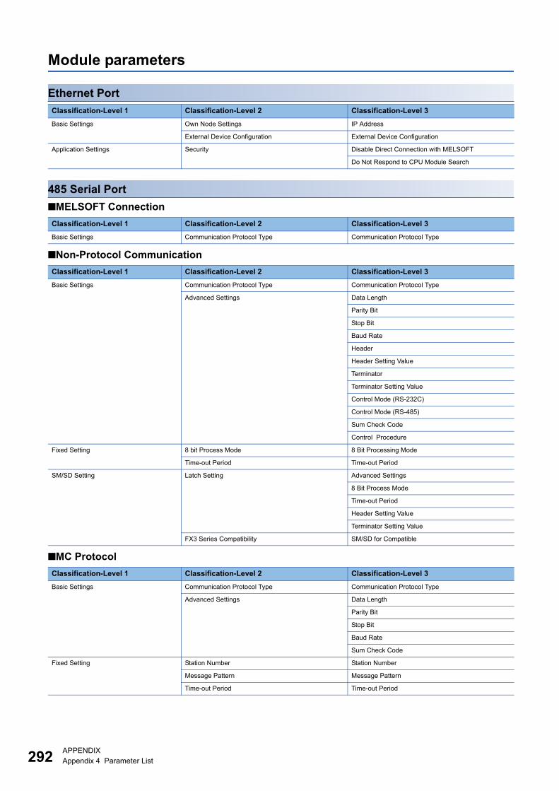
292APPENDIX
Appendix 4 Parameter List
Module parameters
Ethernet Port
485 Serial Port
■MELSOFT Connection
■Non-Protocol Communication
■MC Protocol
Classification-Level 1 Classification-Level 2 Classification-Level 3
Basic Settings Own Node Settings IP Address
External Device Configuration External Device Configuration
Application Settings Security Disable Direct Connection with MELSOFT
Do Not Respond to CPU Module Search
Classification-Level 1 Classification-Level 2 Classification-Level 3
Basic Settings Communication Protocol Type Communication Protocol Type
Classification-Level 1 Classification-Level 2 Classification-Level 3
Basic Settings Communication Protocol Type Communication Protocol Type
Advanced Settings Data Length
Parity Bit
Stop Bit
Baud Rate
Header
Header Setting Value
Terminator
Terminator Setting Value
Control Mode (RS-232C)
Control Mode (RS-485)
Sum Check Code
Control Procedure
Fixed Setting 8 bit Process Mode 8 Bit Processing Mode
Time-out Period Time-out Period
SM/SD Setting Latch Setting Advanced Settings
8 Bit Process Mode
Time-out Period
Header Setting Value
Terminator Setting Value
FX3 Series Compatibility SM/SD for Compatible
Classification-Level 1 Classification-Level 2 Classification-Level 3
Basic Settings Communication Protocol Type Communication Protocol Type
Advanced Settings Data Length
Parity Bit
Stop Bit
Baud Rate
Sum Check Code
Fixed Setting Station Number Station Number
Message Pattern Message Pattern
Time-out Period Time-out Period
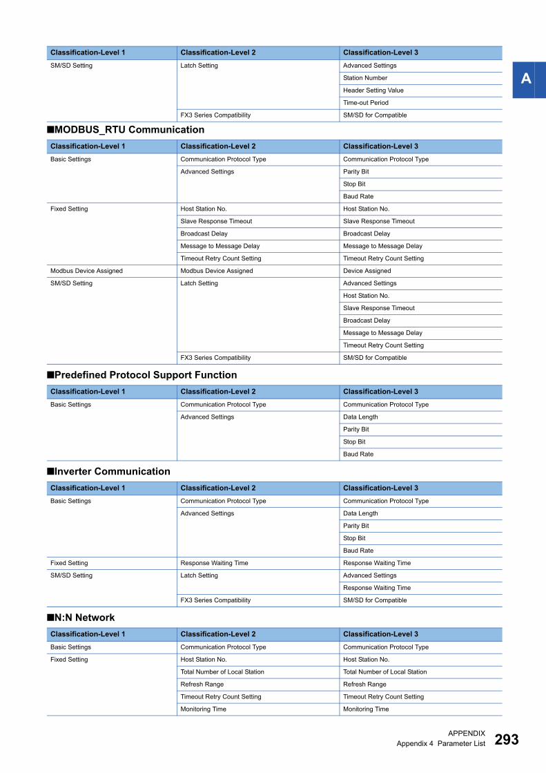
APPENDIX
Appendix 4 Parameter List 293
A
■MODBUS_RTU Communication
■Predefined Protocol Support Function
■Inverter Communication
■N:N Network
SM/SD Setting Latch Setting Advanced Settings
Station Number
Header Setting Value
Time-out Period
FX3 Series Compatibility SM/SD for Compatible
Classification-Level 1 Classification-Level 2 Classification-Level 3
Basic Settings Communication Protocol Type Communication Protocol Type
Advanced Settings Parity Bit
Stop Bit
Baud Rate
Fixed Setting Host Station No. Host Station No.
Slave Response Timeout Slave Response Timeout
Broadcast Delay Broadcast Delay
Message to Message Delay Message to Message Delay
Timeout Retry Count Setting Timeout Retry Count Setting
Modbus Device Assigned Modbus Device Assigned Device Assigned
SM/SD Setting Latch Setting Advanced Settings
Host Station No.
Slave Response Timeout
Broadcast Delay
Message to Message Delay
Timeout Retry Count Setting
FX3 Series Compatibility SM/SD for Compatible
Classification-Level 1 Classification-Level 2 Classification-Level 3
Basic Settings Communication Protocol Type Communication Protocol Type
Advanced Settings Data Length
Parity Bit
Stop Bit
Baud Rate
Classification-Level 1 Classification-Level 2 Classification-Level 3
Basic Settings Communication Protocol Type Communication Protocol Type
Advanced Settings Data Length
Parity Bit
Stop Bit
Baud Rate
Fixed Setting Response Waiting Time Response Waiting Time
SM/SD Setting Latch Setting Advanced Settings
Response Waiting Time
FX3 Series Compatibility SM/SD for Compatible
Classification-Level 1 Classification-Level 2 Classification-Level 3
Basic Settings Communication Protocol Type Communication Protocol Type
Fixed Setting Host Station No. Host Station No.
Total Number of Local Station Total Number of Local Station
Refresh Range Refresh Range
Timeout Retry Count Setting Timeout Retry Count Setting
Monitoring Time Monitoring Time
Classification-Level 1 Classification-Level 2 Classification-Level 3
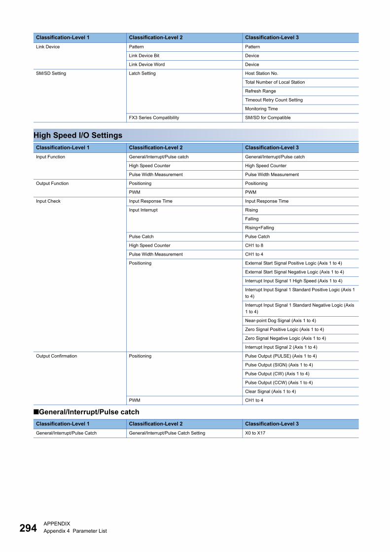
294APPENDIX
Appendix 4 Parameter List
High Speed I/O Settings
■General/Interrupt/Pulse catch
Link Device Pattern Pattern
Link Device Bit Device
Link Device Word Device
SM/SD Setting Latch Setting Host Station No.
Total Number of Local Station
Refresh Range
Timeout Retry Count Setting
Monitoring Time
FX3 Series Compatibility SM/SD for Compatible
Classification-Level 1 Classification-Level 2 Classification-Level 3
Input Function General/Interrupt/Pulse catch General/Interrupt/Pulse catch
High Speed Counter High Speed Counter
Pulse Width Measurement Pulse Width Measurement
Output Function Positioning Positioning
PWM PWM
Input Check Input Response Time Input Response Time
Input Interrupt Rising
Falling
Rising+Falling
Pulse Catch Pulse Catch
High Speed Counter CH1 to 8
Pulse Width Measurement CH1 to 4
Positioning External Start Signal Positive Logic (Axis 1 to 4)
External Start Signal Negative Logic (Axis 1 to 4)
Interrupt Input Signal 1 High Speed (Axis 1 to 4)
Interrupt Input Signal 1 Standard Positive Logic (Axis 1
to 4)
Interrupt Input Signal 1 Standard Negative Logic (Axis
1 to 4)
Near-point Dog Signal (Axis 1 to 4)
Zero Signal Positive Logic (Axis 1 to 4)
Zero Signal Negative Logic (Axis 1 to 4)
Interrupt Input Signal 2 (Axis 1 to 4)
Output Confirmation Positioning Pulse Output (PULSE) (Axis 1 to 4)
Pulse Output (SIGN) (Axis 1 to 4)
Pulse Output (CW) (Axis 1 to 4)
Pulse Output (CCW) (Axis 1 to 4)
Clear Signal (Axis 1 to 4)
PWM CH1 to 4
Classification-Level 1 Classification-Level 2 Classification-Level 3
General/Interrupt/Pulse Catch General/Interrupt/Pulse Catch Setting X0 to X17
Classification-Level 1 Classification-Level 2 Classification-Level 3
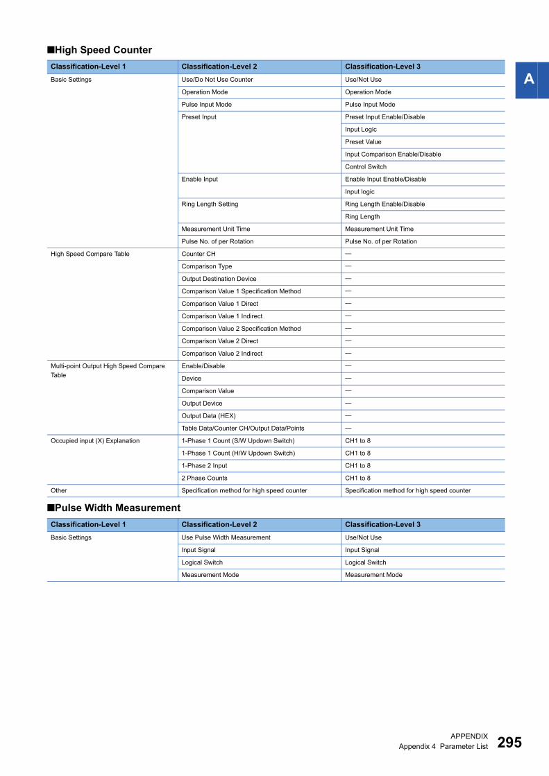
APPENDIX
Appendix 4 Parameter List 295
A
■High Speed Counter
■Pulse Width Measurement
Classification-Level 1 Classification-Level 2 Classification-Level 3
Basic Settings Use/Do Not Use Counter Use/Not Use
Operation Mode Operation Mode
Pulse Input Mode Pulse Input Mode
Preset Input Preset Input Enable/Disable
Input Logic
Preset Value
Input Comparison Enable/Disable
Control Switch
Enable Input Enable Input Enable/Disable
Input logic
Ring Length Setting Ring Length Enable/Disable
Ring Length
Measurement Unit Time Measurement Unit Time
Pulse No. of per Rotation Pulse No. of per Rotation
High Speed Compare Table Counter CH
Comparison Type
Output Destination Device
Comparison Value 1 Specification Method
Comparison Value 1 Direct
Comparison Value 1 Indirect
Comparison Value 2 Specification Method
Comparison Value 2 Direct
Comparison Value 2 Indirect
Multi-point Output High Speed Compare
Table
Enable/Disable
Device
Comparison Value
Output Device
Output Data (HEX)
Table Data/Counter CH/Output Data/Points
Occupied input (X) Explanation 1-Phase 1 Count (S/W Updown Switch) CH1 to 8
1-Phase 1 Count (H/W Updown Switch) CH1 to 8
1-Phase 2 Input CH1 to 8
2 Phase Counts CH1 to 8
Other Specification method for high speed counter Specification method for high speed counter
Classification-Level 1 Classification-Level 2 Classification-Level 3
Basic Settings Use Pulse Width Measurement Use/Not Use
Input Signal Input Signal
Logical Switch Logical Switch
Measurement Mode Measurement Mode
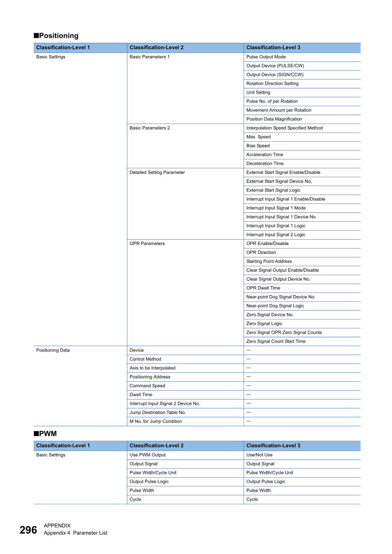
296APPENDIX
Appendix 4 Parameter List
■Positioning
■PWM
Classification-Level 1 Classification-Level 2 Classification-Level 3
Basic Settings Basic Parameters 1 Pulse Output Mode
Output Device (PULSE/CW)
Output Device (SIGN/CCW)
Rotation Direction Setting
Unit Setting
Pulse No. of per Rotation
Movement Amount per Rotation
Position Data Magnification
Basic Parameters 2 Interpolation Speed Specified Method
Max. Speed
Bias Speed
Acceleration Time
Deceleration Time
Detailed Setting Parameter External Start Signal Enable/Disable
External Start Signal Device No.
External Start Signal Logic
Interrupt Input Signal 1 Enable/Disable
Interrupt Input Signal 1 Mode
Interrupt Input Signal 1 Device No.
Interrupt Input Signal 1 Logic
Interrupt Input Signal 2 Logic
OPR Parameters OPR Enable/Disable
OPR Direction
Starting Point Address
Clear Signal Output Enable/Disable
Clear Signal Output Device No.
OPR Dwell Time
Near-point Dog Signal Device No.
Near-point Dog Signal Logic
Zero Signal Device No.
Zero Signal Logic
Zero Signal OPR Zero Signal Counts
Zero Signal Count Start Time
Positioning Data Device
Control Method
Axis to be Interpolated
Positioning Address
Command Speed
Dwell Time
Interrupt Input Signal 2 Device No.
Jump Destination Table No.
M No. for Jump Condition
Classification-Level 1 Classification-Level 2 Classification-Level 3
Basic Settings Use PWM Output Use/Not Use
Output Signal Output Signal
Pulse Width/Cycle Unit Pulse Width/Cycle Unit
Output Pulse Logic Output Pulse Logic
Pulse Width Pulse Width
Cycle Cycle
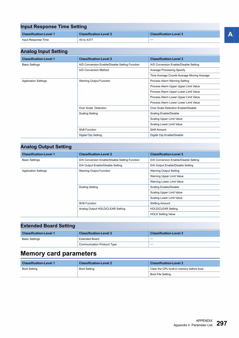
APPENDIX
Appendix 4 Parameter List 297
A
Input Response Time Setting
Analog Input Setting
Analog Output Setting
Extended Board Setting
Memory card parameters
Classification-Level 1 Classification-Level 2 Classification-Level 3
Input Response Time X0 to X377
Classification-Level 1 Classification-Level 2 Classification-Level 3
Basic Settings A/D Conversion Enable/Disable Setting Function A/D Conversion Enable/Disable Setting
A/D Conversion Method Average Processing Specify
Time Average Counts Average Moving Average
Application Settings Warning Output Function Process Alarm Warning Setting
Process Alarm Upper Upper Limit Value
Process Alarm Upper Lower Limit Value
Process Alarm Lower Upper Limit Value
Process Alarm Lower Lower Limit Value
Over Scale Detection Over Scale Detection Enable/Disable
Scaling Setting Scaling Enable/Disable
Scaling Upper Limit Value
Scaling Lower Limit Value
Shift Function Shift Amount
Digital Clip Setting Digital Clip Enable/Disable
Classification-Level 1 Classification-Level 2 Classification-Level 3
Basic Settings D/A Conversion Enable/Disable Setting Function D/A Conversion Enable/Disable Setting
D/A Output Enable/Disable Setting D/A Output Enable/Disable Setting
Application Settings Warning Output Function Warning Output Setting
Warning Upper Limit Value
Warning Lower Limit Value
Scaling Setting Scaling Enable/Disable
Scaling Upper Limit Value
Scaling Lower Limit Value
Shift Function Shifting Amount
Analog Output HOLD/CLEAR Setting HOLD/CLEAR Setting
HOLD Setting Value
Classification-Level 1 Classification-Level 2 Classification-Level 3
Basic Settings Extended Board
Communication Protocol Type
Classification-Level 1 Classification-Level 2 Classification-Level 3
Boot Setting Boot Setting Clear the CPU built-in memory before boot
Boot File Setting
298
INDEX
A
Annunciator (F) . . . . . . . . . . . . . . . . . . . . . . . . 206
B
Boot operation . . . . . . . . . . . . . . . . . . . . . . . . 104Built-in analog. . . . . . . . . . . . . . . . . . . . . . . . . 201
C
Character string constant . . . . . . . . . . . . . . . . . 221Clock function. . . . . . . . . . . . . . . . . . . . . . . . . . 46Constant . . . . . . . . . . . . . . . . . . . . . . . . . . . . 221Constant scan . . . . . . . . . . . . . . . . . . . . . . . . . 84Counter (C/LC) . . . . . . . . . . . . . . . . . . . . . . . . 212CPU parameter. . . . . . . . . . . . . . . . . . . . . . . . 291
D
Data memory . . . . . . . . . . . . . . . . . . . . . . . . . . 37Data register (D) . . . . . . . . . . . . . . . . . . . . . . . 215Decimal . . . . . . . . . . . . . . . . . . . . . . . . . . . . . 221Decimal constant (K) . . . . . . . . . . . . . . . . . . . . 221Device initial value . . . . . . . . . . . . . . . . . . . . . . 97Device/label access service processing setting . 107Device/label memory . . . . . . . . . . . . . . . . . . . . . 37
E
END processing . . . . . . . . . . . . . . . . . . . . . . . . 17Error code . . . . . . . . . . . . . . . . . . . . . . . . . . . 274Event execution type program . . . . . . . . . . . . . . 25Execution type of program . . . . . . . . . . . . . . . . . 20
F
File password 32. . . . . . . . . . . . . . . . . . . . . . . 113File register (R). . . . . . . . . . . . . . . . . . . . . . . . 218Files . . . . . . . . . . . . . . . . . . . . . . . . . . . . . . . . 39Fixed scan execution mode . . . . . . . . . . . . . . . . 23Fixed scan execution type program. . . . . . . . . . . 21FX3-compatible high-speed counter . . . . . . . . . 165FX3-compatible pulse catch . . . . . . . . . . . . . . . 188
G
Global pointer . . . . . . . . . . . . . . . . . . . . . . . . . 219
H
Hexadecimal . . . . . . . . . . . . . . . . . . . . . . . . . 221Hexadecimal constant (H) . . . . . . . . . . . . . . . . 221High-speed comparison table . . . . . . . . . . . . . . 132High-speed counter . . . . . . . . . . . . . . . . . . . . . 114High-speed counter (normal mode) . . . . . . . . . . 124High-speed counter
(pulse density measurement mode) . . . . . . . . . 126High-speed counter
(rotational speed measurement mode) . . . . . . . 129High-speed timer . . . . . . . . . . . . . . . . . . . . . . 209
I
I/O refresh . . . . . . . . . . . . . . . . . . . . . . . . . . . . .17Index register setting. . . . . . . . . . . . . . . . . . . . .217Index registers (Z/LZ) . . . . . . . . . . . . . . . . . . . .217Initial device value . . . . . . . . . . . . . . . . . . . . . . .97Initial execution type program . . . . . . . . . . . . . . .20Initial scan time . . . . . . . . . . . . . . . . . . . . . . . . .18Input (X) . . . . . . . . . . . . . . . . . . . . . . . . . . . . .205Internal relay (M) . . . . . . . . . . . . . . . . . . . . . . .206Interrupt cause . . . . . . . . . . . . . . . . . . . . . . . . .220Interrupt pointer (I) . . . . . . . . . . . . . . . . . . . . . .219Interrupt priority . . . . . . . . . . . . . . . . . . . . . . . .220Interrupt program . . . . . . . . . . . . . . . . . . . . . . . .30
L
Label. . . . . . . . . . . . . . . . . . . . . . . . . . . . . . . .222Latch. . . . . . . . . . . . . . . . . . . . . . . . . . . . . . . . .99Latch (1) . . . . . . . . . . . . . . . . . . . . . . . . . . . . . .99Latch (2) . . . . . . . . . . . . . . . . . . . . . . . . . . . . . .99Latch clear . . . . . . . . . . . . . . . . . . . . . . . . . . . .101Latch relay (L) . . . . . . . . . . . . . . . . . . . . . . . . .206Link register (W) . . . . . . . . . . . . . . . . . . . . . . . .215Link relay (B) . . . . . . . . . . . . . . . . . . . . . . . . . .206Link special register (SW) . . . . . . . . . . . . . . . . .215Link special relay (SB). . . . . . . . . . . . . . . . . . . .208Low-speed timer . . . . . . . . . . . . . . . . . . . . . . . .209
M
Memory card parameter . . . . . . . . . . . . . . . . . .297Memory configuration . . . . . . . . . . . . . . . . . . . . .37Module access device . . . . . . . . . . . . . . . . . . . .216Module parameter . . . . . . . . . . . . . . . . . . . . . .292Multiple interrupt. . . . . . . . . . . . . . . . . . . . . . . . .53Multiple point output, high-speed comparison table . .134
N
Nesting (N) . . . . . . . . . . . . . . . . . . . . . . . . . . .218
O
Online change . . . . . . . . . . . . . . . . . . . . . . . . . .50Output (Y) . . . . . . . . . . . . . . . . . . . . . . . . . . . .205
P
PAUSE . . . . . . . . . . . . . . . . . . . . . . . . . . . . . . .35PID control. . . . . . . . . . . . . . . . . . . . . . . . . . . . .55Pointer (P) . . . . . . . . . . . . . . . . . . . . . . . . . . . .219Priority for interrupt cause . . . . . . . . . . . . . . . . .220Pulse catch . . . . . . . . . . . . . . . . . . . . . . . . . . .184Pulse width measurement . . . . . . . . . . . . . . . . .174PWM . . . . . . . . . . . . . . . . . . . . . . . . . . . . . . . .193
R
Real constant (E) . . . . . . . . . . . . . . . . . . . . . . .221Remote operation . . . . . . . . . . . . . . . . . . . . . . . .86Remote PAUSE . . . . . . . . . . . . . . . . . . . . . . . . .88
299
I
Remote RESET . . . . . . . . . . . . . . . . . . . . . . . . 89Remote RUN . . . . . . . . . . . . . . . . . . . . . . . . . . 86Remote STOP . . . . . . . . . . . . . . . . . . . . . . . . . 86Retentive timer (ST) . . . . . . . . . . . . . . . . . . . . 209Routine timer . . . . . . . . . . . . . . . . . . . . . . . . . 209RUN status. . . . . . . . . . . . . . . . . . . . . . . . . . . . 35
S
Scan execution type program . . . . . . . . . . . . . . . 21Scan monitoring function . . . . . . . . . . . . . . . . . . 44Scan time. . . . . . . . . . . . . . . . . . . . . . . . . . . . . 18Scan time monitoring time setting . . . . . . . . . . . . 44SD memory card . . . . . . . . . . . . . . . . . . . . . . . . 38SD memory card forced stop . . . . . . . . . . . . . . 103Security function . . . . . . . . . . . . . . . . . . . . . . . 113Security key authentication . . . . . . . . . . . . . . . 113Special register (SD) . . . . . . . . . . . . . . . . . . . . 215Special relay (SM). . . . . . . . . . . . . . . . . . . . . . 215Stand-by type program . . . . . . . . . . . . . . . . . . . 28Step relay (S) . . . . . . . . . . . . . . . . . . . . . . . . . 208STOP status. . . . . . . . . . . . . . . . . . . . . . . . . . . 35Subroutine program . . . . . . . . . . . . . . . . . . . . . 29System clock . . . . . . . . . . . . . . . . . . . . . . . . . . 49System device . . . . . . . . . . . . . . . . . . . . . . . . 215System parameter. . . . . . . . . . . . . . . . . . . . . . 291
T
Time setting . . . . . . . . . . . . . . . . . . . . . . . . . . . 46Time zone . . . . . . . . . . . . . . . . . . . . . . . . . . . . 48Timer (T/ST). . . . . . . . . . . . . . . . . . . . . . . . . . 209
U
User device . . . . . . . . . . . . . . . . . . . . . . . . . . 205
W
Watchdog timer . . . . . . . . . . . . . . . . . . . . . . . . 44
300
REVISIONS
2014 MITSUBISHI ELECTRIC CORPORATION
Revision date Revision Description
October 2014 A First Edition
January 2015 B ■Added functions
Fixed scan execution type program, Online change, PID control function, FX3-compatible high-
speed counter function, Routine timer
■Added or modified parts
Section 1.3, 3.1, 3.2, Chapter 4, 7, 8, 9, 12, 13, 17, Section 19.2, Chapter 20, Section 21.2,
Appendix 1, 2, 3, 4
This manual confers no industrial property rights or any rights of any other kind, nor does it confer any patent licenses. Mitsubishi Electric Corporation cannot
be held responsible for any problems involving industrial property rights which may occur as a result of using the contents noted in this manual.
301
WARRANTY
1.
Please confirm the following product warranty details before using this product.
[Gratis Warranty Term]
If any faults or defects (hereinafter "Failure") found to be the responsibility of Mitsubishi occurs during use of the product within the gratis warranty term, the product shall be repaired at no cost via the sales representative or Mitsubishi Service Company. However, if repairs are required onsite at domestic or overseas location, expenses to send an engineer will be solely at the customer's discretion. Mitsubishi shall not be held responsible for any re-commissioning, maintenance, or testing on-site that involves replacement of the failed module.
Overseas, repairs shall be accepted by Mitsubishi's local overseas FA Center. Note that the repair conditions at each FA Center may differ.
The gratis warranty term of the product shall be for one year after the date of purchase or delivery to a designated place. Note that after manufacture and shipment from Mitsubishi, the maximum distribution period shall be six (6) months, and the longest gratis warranty term after manufacturing shall be eighteen (18) months. The gratis warranty term of repair parts shall not exceed the gratis warranty term before repairs.
[Gratis Warranty Range]
The range shall be limited to normal use within the usage state, usage methods and usage environment, etc., which follow the conditions and precautions, etc., given in the instruction manual, user's manual and caution labels on the product.
1)
Even within the gratis warranty term, repairs shall be charged for in the following cases.
2)
Failure occurring from inappropriate storage or handling, carelessness or negligence by the user. Failure caused by the user's hardware or software design.
a)
Failure caused by unapproved modifications, etc., to the product by the user.
b)
Mitsubishi shall accept onerous product repairs for seven (7) years after production of the product is discontinued.Discontinuation of production shall be notified with Mitsubishi Technical Bulletins, etc.
1)
Product supply (including repair parts) is not available after production is discontinued.
2)
In using the Mitsubishi MELSEC programmable controller, the usage conditions shall be that the application will not lead to a major accident even if any problem or fault should occur in the programmable controller device, and that backup and fail-safe functions are systematically provided outside of the device for any problem or fault.
1)
The Mitsubishi programmable controller has been designed and manufactured for applications in general industries, etc. Thus, applications in which the public could be affected such as in nuclear power plants and other power plants operated by respective power companies, and applications in which a special quality assurance system is required, such as for railway companies or public service purposes shall be excluded from the programmable controller applications. In addition, applications in which human life or property that could be greatly affected, such as in aircraft, medical applications, incineration and fuel devices, manned transportation, equipment for recreation and amusement, and safety devices, shall also be excluded from the programmable controller range of applications. However, in certain cases, some applications may be possible, providing the user consults their local Mitsubishi representative outlining the special requirements of the project, and providing that all parties concerned agree to the special circumstances, solely at the user's discretion.
2)When the Mitsubishi product is assembled into a user's device, Failure that could have been avoided if functions or structures, judged as necessary in the legal safety measures the user's device is subject to or as necessary by industry standards, had been provided.
c)
Failure that could have been avoided if consumable parts (battery, backlight, fuse, etc.) designated in the instruction manual had been correctly serviced or replaced.
d)
Relay failure or output contact failure caused by usage beyond the specified life of contact (cycles).
e)
Failure caused by external irresistible forces such as fires or abnormal voltages, and failure caused by force majeure such as earthquakes, lightning, wind and water damage.
f)
Failure caused by reasons unpredictable by scientific technology standards at time of shipment from Mitsubishi.
g)
Any other failure found not to be the responsibility of Mitsubishi or that admitted not to be so by the user.
h)
2. Onerous repair term after discontinuation of production
Gratis Warranty Term and Gratis Warranty Range
4. Exclusion of loss in opportunity and secondary loss from warranty liability
3. Overseas service
The specifications given in the catalogs, manuals or technical documents are subject to change without prior notice.
5. Changes in product specifications
6. Product application
Regardless of the gratis warranty term, Mitsubishi shall not be liable for compensation of damages caused by any cause found not to be the responsibility of Mitsubishi, loss in opportunity, lost profits incurred to the user or third person by failure of Mitsubishi products, special damages and secondary damages whether foreseeable or not, compensation for accidents, and compensation for damages to products other than Mitsubishi products, replacement by the user, maintenance of on-site equipment, start-up test run and other tasks.
302
TRADEMARKSMicrosoft and Windows are either registered trademarks or trademarks of Microsoft Corporation in the United States and/or
other countries.
Ethernet is a trademark of Xerox Corporation.
MODBUS is a registered trademark of Schneider Electric SA.
SD logo and SDHC logo are trademarks or registered trademarks of SD-3C, LLC.
The company name and the product name to be described in this manual are the registered trademarks or trademarks of
each company.


HEAD OFFICE: TOKYO BUILDING, 2-7-3 MARUNOUCHI, CHIYODA-KU, TOKYO 100-8310, JAPAN
HIMEJI WORKS: 840, CHIYODA MACHI, HIMEJI, JAPAN
Specifications are subject to change without notice.
When exported from Japan, this manual does not require application to the
Ministry of Economy, Trade and Industry for service transaction permission.
Manual number: JY997D55401B
Model: FX5-U-OU-E
Model code: 09R537


![MELSEC iQ-F FX5-40SSC-S Hardware Manual - Electrobit … · Hardware manual (This manual) FX5-40SSC-S 200 mm ... AX3, AX4) [5] POWER LED [6] RUN LED [7] ERROR LED [8 ... For further](https://img.dokumen.tips/doc/110x75/5ac30ef97f8b9aa0518be5dd/melsec-iq-f-fx5-40ssc-s-hardware-manual-electrobit-manual-this-manual-fx5-40ssc-s.jpg)