Embed Size (px)
Citation preview
Supplementary information
Transforming the cost of solar-to-electrical energy conversion: Integrating
thin-film GaAs solar cells with non-tracking mini-concentrators
Kyusang Lee1, Jaesang Lee1, Bryan A. Mazor2, and Stephen R. Forrest 1, 2, 3
1 Department of Electrical Engineering and Computer Science, University of Michigan, Ann Arbor, MI
48109, USA
2 Department of Physics, University of Michigan, Ann Arbor, MI 48109, USA
3 Department of Material Science and Engineering, University of Michigan, Ann Arbor, MI 48109, USA
*e-mail: [email protected]
Contents
1. Laser dicing of thin-film GaAs solar cells on plastic sheets
2. Self-aligned transfer printing of thin-film GaAs solar cells onto plastic concentrators
3. Mini-compound parabolic concentrator (CPC) design
4. Characteristics of thin-film GaAs solar cells under concentrated light
5. Comparison of solar cell operation temperature under 1 sun illumination
6. Optimum alignment of CPCs
7. Calculation of hourly, daily and yearly energy harvesting trends
8. Production cost estimates
1

1. Laser dicing of thin-film GaAs solar cells on plastic sheet
A CO2 laser engraving and cutting system (X-660 superspeed-600, Universal Laser Systems,
Inc., Scottsdale, AZ) is used to dice the non-destructive epitaxial lift-off (ND-ELO) processed
thin-film GaAs solar cells bonded to a Kapton® sheet. To confirm the feasibility of the laser
dicing process, linear and zig-zag cut patterns, with 750 μm and 500 μm spacing between the
active solar cell active areas, respectively, are demonstrated (Figure S1(a) and (b)). Improved
material utilization by reducing the 300 μm kerf is possible. Supplementary video 1 and 2 show
the dicing process of each pattern. Figure S1(c) and (d) shows the area loss due to the cut
geometry. For 6 inch wafers, the area loss is ~27 % and 6.2 % for single square and bar shaped
cuts, respectively. Therefore, the wafer material utilization is improved by ~21 % by increasing
the cell packing density.
2. Self-aligned transfer printing of thin-film GaAs solar cells onto plastic CPCs
The acrylonitrile butadiene styrene (ABS) mold for the polydimethylsiloxane (PDMS) stamp
used to integrate and align the thin-film GaAs solar cells with plastic mini-CPCs is fabricated
using a 3D printer (Dimension Elite, Stratasys, Eden Praire, MN). Figure S2(a) shows the
detailed dimensions and photographs of the mold for the PDMS stamp, which is designed to
exactly fit into the CPC opening shown in Figure S2(b). An additional 3D printed mold is used
to align the solar cell strips for pick-up by the PDMS stamp. The pyramid shape of the PDMS
stamp prevents direct contact between the stamp and the side walls of the CPC so that pressure
for bonding the solar cells is only applied onto the CPC base. Figure S2(c) is a schematic of the
fit between the stamps and CPCs.
2

3. Mini-compound parabolic concentrator (CPC) design
Figure S3(a) and (b) show schematics for a CPC comprised of two parabolas with tilted axes at
an angle equal to its acceptance angle1. The plastic mini-CPCs are 2D, half cylinders to eliminate
the need for solar tracking along its longitudinal axis. Figure S3(c) shows the effect of CPC
truncation on the acceptance angle and concentration factor, CF. A non-truncated CPC shows the
highest CF with no light collection outside of the acceptance angle. Although the CF is reduced
with increased truncation, it is nevertheless able to collect light at much broader angles than the
acceptance angle.
Ray tracing using Matlab software (MathWorks, Natick, MA) was used to determine the
CF. The geometry of the CPC is defined in Cartesian coordinates, and its four vertices are
calculated using base width (defined by the dimensions of the GaAs solar cell), height, and
acceptance angle. Note that the focal points of the two parabolas comprising the CPC form the
base edges. We choose practical CPC heights (~8% of the untruncated CPC), where truncation
alters the acceptance of input rays incident on CPC, and hence the CF. We assume that the input
rays are parallel.
Now, CF is the ratio of photons incident on solar cell with CPC, to that without it. Due to
the symmetry of the CPC about its central axis, only positive solar incident angles were
considered, i.e., 0 < θsun < θmax, where θsun is the angle of the rays with respect to the central axis
of CPC, and θmax is the angle at which all incident rays are shadowed and thus, . Greater
than 10,000 spatially distributed rays for each angle were used. When a ray is reflected by the
CPC, its intensity is reduced by the reflectance of Ag, which was measured on PETG using a
variable-angle spectroscopic ellipsometer (VASE, J.A. Woollam, Lincoln, NE) and a
UV/Vis/NIR Spectrophotometer (LAMBDA 1050, Perkin Elmer, Waltham, MA). The range of
3
wavelengths and angles was 300 nm to 900 nm with 3 nm steps, and from 15 o to 85 o with 5o
steps. The values between those measured are interpolated. Then, the wavelength and incident
angle dependent reflectance is weighted by the AM1.5G solar spectrum. Finally, CF vs. θsun and
acceptance angle is calculated.
Figure S3(d) and (e) show contour plots of CF vs. incident angle calculated for various
CPC shapes. Figure S3(d) shows the case of a non-truncated CPC where CF increases as the
angle between each parabola axis (i.e. the acceptance angle) decreases. Figure S3(e) shows the
case of CPCs with a fixed aspect ratio of 4 (CPC height/solar cell width) such that the truncation
ratio depends on acceptance angle. The truncation ratios of CPCs with narrow acceptance angles
are higher than for wide acceptance angles.
4. Characteristics of thin-film GaAs solar cells under the concentrated light
Figure S4(a)-(d) summarize the performance of the thin-film ND-ELO GaAs solar cells under
various concentrated light conditions. The solar cells are integrated with the mini-CPCs and are
measured using a solar simulator calibrated to AM 1.5G illumination at 1 sun (100 mW cm-2)
using a Si photodiode. Short circuit current (Jsc), Open circuit voltage (Voc), fill factor, and power
conversion efficiency (PCE) are extracted from the I-V characteristics (Figure 2(a)). The
measurement shows the power conversion efficiency of the cell integrated with a 6° tilted CPC
with CF= 3.3 is slightly improved (~0.5 %) compared to a non-concentrated device with one due
to the increased open circuit voltage, Voc, at higher intensities.
5. Comparison of solar cell operation temperature under 1 sun illumination
4

Figure S5 shows the operating temperatures of thin-film and substrate-based GaAs solar cells
under simulated AM 1.5G, 1 sun intensity (100mW cm-2) illumination. After 250 s, the substrate-
based GaAs solar cells operate around 45℃ as predicted2, whereas the thin-film cells operate at
28℃. Supplementary videos 3 and 4 show the operating temperatures of thin-film and substrate-
based solar cells under 1 sun and 3.3 sun illumination, as measured by an IR camera (A325,
FLIR, Wilmington, NC).
6. Optimum alignment of CPCs
Figure S6(a) and (b) shows east-west and north-south axis longitudinal CPC alignments. For
north-south alignment, the CPC only collects light when the sun lies within the acceptance angle
of the CPC; however, the east-west axis alignment provides a wide coverage of sunlight
throughout the day by tilting it toward the solar declination path. The position of the CPC needs
to be adjusted only 4 times per year for optimum energy harvesting since the acceptance angle of
the CPC is sufficiently wide to cover the seasonal changes in the solar path.
To maximize the energy harvesting throughout the year, at Phoenix, AZ (33.4N,
112.1W), we first calculate the optimum seasonal alignment. Solar radiation intensity is then
determined using time dependent zenith angles and air mass for each day of the year . Diffuse
light is not considered for the calculation. The daily energy generation is then integrated over the
entire year. The device tilt is iteratively changed, to generate a full contour mapping of the
energy generation as both a function of southward tilt and day of the year.
Figure S6(c), (d) and (e) show the daily energy generated using the measured angle
dependent CFs for a non-concentrated and a cell with 6°tilted a CPC aligned along north-south
and east-west axes. Using the seasonal position shift of the solar path, we find the optimum CPC
5
facing angle by maximizing the integrated energy generation with varying alignment angle. The
optimum seasonal positions are summarized in Figure S6 (f).
7. Calculation of hourly, daily and yearly energy harvesting trends
To calculate the hourly, daily and yearly energy generation of thin-film GaAs solar cells with the
plastic mini-CPCs, the air mass and zenith angle of the solar radiation are calculated at Phoenix,
AZ. The solar position is calculated for every day of the year, and at 500 times during each day.
The radiation incident on the device is calculated based on the air mass at that time. Figure S7(a)
shows the hourly air mass and solar angles for two specific dates. Hourly and daily radiation
intensity values, and the incident angle on the CPC are determined based on these calculations.
Figure S7(b)-(e) shows hourly and daily energy harvesting patterns of the thin-film
GaAs solar cells with and without east-west aligned CPCs for four seasonal alignments per year.
The CPC with a narrow acceptance angle shows high energy harvesting at specific dates but, is
not able to completely cover the seasonal solar path. In contrast, CPCs with wider acceptance
angles show almost full coverage of solar path, although it shows a relatively low CF. The
optimum design employs a 9.5° tilted CPC although the 6° tilted CPC shows the best annual
energy harvesting performance from the experimentally measured concentration factors due to
an imperfect CPC shape and reflectance of the Ag film on PETG. Figure S7(f) shows the energy
harvesting based on angle dependent CFs measured using a 6° tilted CPC.
Figure S8(a) and (b) show the energy harvesting on two specific dates during winter and
summer, respectively, using a 6° tilted CPC. The wide acceptance angle enables the CPC to
cover most of the useful daylight with low air mass. From the integration of hourly energy
harvesting curves for thin-film GaAs solar cells with and without a CPC, we confirm that the
6
ND-ELO processed solar cells integrated with a 6° tilted CPC shows 2.8 and 2.7 times higher
energy harvesting compared with non-concentrated cells on January 1st and July 1st, respectively
(Figure S8(c)). Figure S8(d) compares the non-concentrated, and the 2, 3 and 4 tilt positions per
year.
8. Solar module cost estimates3,4
The manufacturing costs for ND-ELO processed thin-film GaAs solar cells are estimated in
USD/peak watt (in current USD and DC power) based on cost analysis from the National
Renewable Energy Laboratory (NREL)3,4. The commercially price for a 6 inch diameter GaAs
wafer is ~$10K /m2 with ~27% area loss in trimming it into a more useful pseudo-square shape.
Through wafer recycling, the cost is reduced to $4.7 Wp-1 and $0.09 Wp
-1 for 10 and 500-times
wafer recycling, respectively, assuming a 24 % cell efficiency3. The loss of wafer area can be
reduced by the increased packing density achieved by the bar shaped solar cells. Another
significant cost is incurred in the chemo-mechanical polishing (CMP) process used in
conventional ELO, which amounts to ~$8 per repolishing at 70 % yield3. This cost can be
completely eliminated by the ND-ELO method which does not employ CMP5. Other
assumptions for U.S. based manufacturing include3: 1) 0.25 labor cost per reactor and 1:0.35
direct:indirect labor ratio. Wages assumed are $12.05 hr-1 and $17.56 hr-1 with 55% benefits for
unskilled and skilled workers. 2) 350 working days per year and 24 working hours per day (3
shifts). 3) $0.07 kW-1 electricity price. 4) $500 m-2 for class 1000 cleanroom cost. 6) 28 %
effective corporate tax rate. Table S1 shows the detailed costs used in comparing each
technology approach (see Methods).
7
To estimate the long term cell production cost, we assume the reference case cost base of
$13.6 Wp-1 by assuming 20× substrate reuse, utilization of 30 % for the III-source and 20 % for
the V source precursors, 15 µm/hr GaAs growth rate, 70 % CMP process yield and 25 % cell
power conversion efficiency. 49 % of this cost originates from the CMP process and the cost of
parent substrate. Therefore, a dramatic cost reduction to $4.6Wp-1 can be achieved simply by
eliminating the CMP process via ND-ELO, and increasing the number of wafer reuses combined
with lower weighted average cost of capital (WACC, 9 % to 7 %) and improved PCE (27 %). As
shown in figure S9(a), this cost can be further reduced to $0.5 Wp-1 by improving cell processing
(enhanced material utilization, deposition rate and yield etc.), and developing manufacturing
processes that lead to reduced material, labor, and depreciation expenses.
The $0.6 Wp-1 module cost is estimated based on the production cost of 2.26 m2
crystalline Si module. For our calculation, the thin-film GaAs solar cell efficiency of 29 % is
adjusted to 24 %, which is the current record module efficiency for the equivalent cell6.
Therefore, an additional cost of $0.12 Wp-1 is incurred. The CPC fabrication cost is estimated at
~$0.01 Wp-1 based on the material cost ($1.05 m-2 for PETG and $2.08 m-2 for 300 nm thick Ag;
therefore, ~$0.003 Wp-1 for PETG and ~$0.007 Wp
-1 for Ag) which is comparable to a
commercially available Ag-coated Mylar substrate with ~95 % reflectance (DuPont Teijin Film,
Chester, VA). By applying an active GaAs solar cell area reduction using CPCs, the total cost for
the completed module is reduced to $0.34 Wp-1 (Figure S9(b)).
8

Fig. S1 Laser dicing of thin-film GaAs solar cells on plastic sheet (a) Linear cutting pattern with 750 μm spacings between
solar cells. (b) Zig-zag cutting pattern with 500 μm spacing between solar cells. Schematic illustration of wafer utilization for (c)
single square cut and (d) multiple small bar shape (2.5 mm × 6.5 mm) cut.
9

Fig. S2 Self-aligned transfer printing process (a) Mold design for the PDMS stamp. Image shows a 3D printed mold. (b) Mold
design for the plastic CPCs. Image shows a mold made from a metal block. (c) Schematic illustration of the fit between the PDMS
stamp and the plastic CPCs for solar cell transfer printing.
10

Fig. S3 Two dimensional mini-compound parabolic concentrator (CPC) design. Schematic illustration of the (a) CPC shape
and (b) 2 dimensional CPCs. (c) Effect of CPC truncation on the acceptance angle and concentration factor. Contour plot of light
incident angle dependent concentration factors for various shapes of (d) non-truncated, and (e) truncated CPCs.
11
Fig. S4 Performance of the thin-film GaAs solar cells under the concentrated light (a) Short circuit current (b) open circuit
voltage, (c) fill factor, and (d) power conversion efficiency of the thin-film GaAs solar cells under the various concentrated light
conditions measured by their integration with the mini-CPCs.
12
Fig. S5 Operating temperature of the thin-film and the substrate GaAs solar cells. Time dependent temperature measured by
IR imaging under 1 sun illumination (100 mW/cm2).
13
Fig. S6 Optimum alignment of CPCs. Schematic of the CPC longitudinal axis aligned along an (a) east-west axis and (b) north-
south axis. Contour plot of energy harvesting for each day, depending on the CPC tilt angle of (c) non-concentrated cell, (d) east-
west axis and (e) north-south aligned CPC. Solid lines indicate optimum seasonal CPC positions and transition dates for maximum
yearly energy harvesting. (f) Summary of optimum seasonal facing angles for each case.
14

Fig. S7 Characterization of hourly, daily and yearly energy harvesting at Phoenix, AZ. (a) Air mass and zenith angle of sunlight calculated on Jan 1st and July 1st. (b) Simulated hourly and daily energy generation for (b) non-concentrated thin-film GaAs solar cells, and the thin-film GaAs solar cells with (c) 5o, (d) 9.5 o and (e) 15 o tilted CPC. (f) Hourly and daily energy harvesting based on measured angle-dependent concentration factors for the thin-film GaAs solar cells integrated with 6o tilted CPC.
15

Fig. S8 Characterization of hourly and annual energy harvesting. Hourly energy generation using thin-film GaAs solar cells with and without a CPC for (a) January 1st and (b) July 1st at Phoenix, AZ. Dashed lines indicate the maximum energy harvesting case using a double axis tracking system. (c) Comparison of daily energy harvesting for January 1st and July 1st by integrating the curves in Fig. S8 (a) and (b). (d) Annual energy harvesting dependence on the number of CPC positions per year.
16
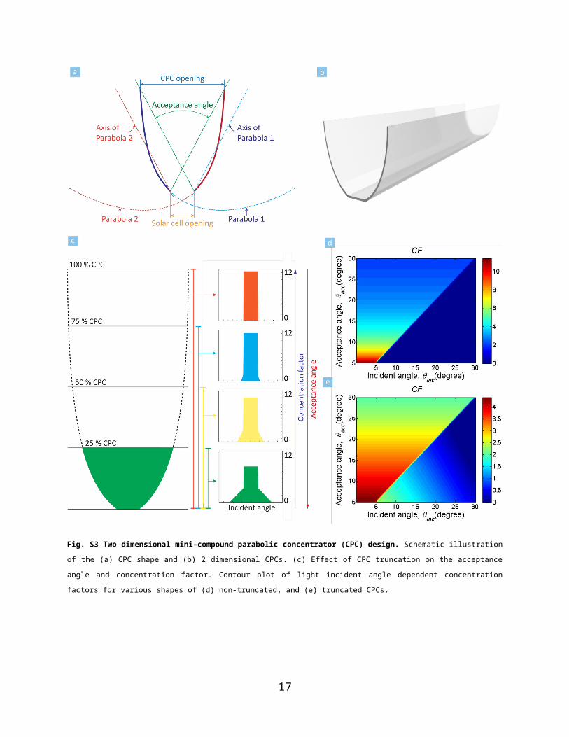
Fig. S9 Production cost estimation (a) Cost estimation for thin-film GaAs solar cells and (b) modules where the cells are integrated with plastic mini-CPCs.
17

Table S1 Production cost estimation. Cost estimation for substrate based, conventional ELO processed, and ND-ELO processed thin-film GaAs solar cells, and module employing integrated plastic mini-CPCs.
* 9% fixed margin is assumed
Fixed CMP cost of $8/repolish with a 70 % process yield is assumed.
18
Substrate cell
ELO processed cell
ND-ELO processed cell
ND-ELO processed cell integrated with
mini-CPCs
Wafer $47.1/Wp $12.37/ Wp $0.94/ Wp $0.34/ Wp
Material $1.62/ Wp $1.25/ Wp $1.25/ Wp $0.45/ Wp
Depreciation $1.8/ Wp $1.8/ Wp $1.8/ Wp $0.64/ Wp
Module cost $0.1/ Wp $0.1/ Wp $0.1/ Wp $0.11/ Wp
Margin* $4.62/ Wp $1.46/ Wp $0.43/ Wp $0.16/ Wp
Etc (laber, utility, maintenance) $0.73/ Wp $0.73/ Wp $0.73/ Wp $0.26/ Wp
Total $55.97/ Wp $17.71/ Wp $5.25/ Wp $1.96/ Wp

References
1. Rabl, A. Optical and thermal properties of compound parabolic concentrators. Sol. Energy 18, 497–511 (1976).
2. Fan, J. C. C. Theoretical temperature dependence of solar cell parameters. Sol. Cells 17, 309–315 (1986).
3. Woodhouse, M. & Goodrich, A. a manufacturing cost analysis relevant to single and dual junction photovoltaic cells fabricated with III-Vs and III-Vs grown on Czochralski Silicon. NREL Rep. No. PR-6A20-60126 92 (2014).)
4. Goodrich, A. et al. A wafer-based monocrystalline silicon photovoltaics road map: Utilizing known technology improvement opportunities for further reductions in manufacturing costs. Sol. Energy Mater. Sol. Cells 114, 110–135 (2013).
5. Lee, K., Zimmerman, J. D., Hughes, T. W. & Forrest, S. R. Non-Destructive Wafer Recycling for Low-Cost Thin-Film Flexible Optoelectronics. Adv. Funct. Mater. 24, 4284–4291 (2014).
6. Green, M. A., Emery, K., Hishikawa, Y., Warta, W. & Dunlop, E. D. Solar cell efficiency tables (version 44). Prog. Photovoltaics Res. Appl. 22, 701–710 (2014).
19